JP2010219549A - 液晶表示装置 - Google Patents
液晶表示装置 Download PDFInfo
- Publication number
- JP2010219549A JP2010219549A JP2010116256A JP2010116256A JP2010219549A JP 2010219549 A JP2010219549 A JP 2010219549A JP 2010116256 A JP2010116256 A JP 2010116256A JP 2010116256 A JP2010116256 A JP 2010116256A JP 2010219549 A JP2010219549 A JP 2010219549A
- Authority
- JP
- Japan
- Prior art keywords
- tft
- film
- thin film
- film transistor
- gate electrode
- Prior art date
- Legal status (The legal status is an assumption and is not a legal conclusion. Google has not performed a legal analysis and makes no representation as to the accuracy of the status listed.)
- Withdrawn
Links
- 239000004973 liquid crystal related substance Substances 0.000 title claims abstract description 39
- 239000000758 substrate Substances 0.000 claims abstract description 52
- 239000010936 titanium Substances 0.000 claims abstract description 34
- 230000015572 biosynthetic process Effects 0.000 claims abstract description 26
- RTAQQCXQSZGOHL-UHFFFAOYSA-N Titanium Chemical compound [Ti] RTAQQCXQSZGOHL-UHFFFAOYSA-N 0.000 claims abstract description 22
- 229910052782 aluminium Inorganic materials 0.000 claims abstract description 22
- XAGFODPZIPBFFR-UHFFFAOYSA-N aluminium Chemical compound [Al] XAGFODPZIPBFFR-UHFFFAOYSA-N 0.000 claims abstract description 22
- 229910052719 titanium Inorganic materials 0.000 claims abstract description 22
- OAICVXFJPJFONN-UHFFFAOYSA-N Phosphorus Chemical compound [P] OAICVXFJPJFONN-UHFFFAOYSA-N 0.000 claims abstract description 20
- 229910052698 phosphorus Inorganic materials 0.000 claims abstract description 20
- 239000011574 phosphorus Substances 0.000 claims abstract description 20
- 239000010949 copper Substances 0.000 claims abstract description 18
- 239000010409 thin film Substances 0.000 claims abstract description 18
- WFKWXMTUELFFGS-UHFFFAOYSA-N tungsten Chemical compound [W] WFKWXMTUELFFGS-UHFFFAOYSA-N 0.000 claims abstract description 18
- 229910052721 tungsten Inorganic materials 0.000 claims abstract description 18
- 239000010937 tungsten Substances 0.000 claims abstract description 18
- XUIMIQQOPSSXEZ-UHFFFAOYSA-N Silicon Chemical compound [Si] XUIMIQQOPSSXEZ-UHFFFAOYSA-N 0.000 claims abstract description 17
- 229910052710 silicon Inorganic materials 0.000 claims abstract description 17
- 239000010703 silicon Substances 0.000 claims abstract description 17
- 229910052715 tantalum Inorganic materials 0.000 claims abstract description 17
- GUVRBAGPIYLISA-UHFFFAOYSA-N tantalum atom Chemical compound [Ta] GUVRBAGPIYLISA-UHFFFAOYSA-N 0.000 claims abstract description 17
- ZOKXTWBITQBERF-UHFFFAOYSA-N Molybdenum Chemical compound [Mo] ZOKXTWBITQBERF-UHFFFAOYSA-N 0.000 claims abstract description 16
- 229910052750 molybdenum Inorganic materials 0.000 claims abstract description 16
- 239000011733 molybdenum Substances 0.000 claims abstract description 16
- RYGMFSIKBFXOCR-UHFFFAOYSA-N Copper Chemical compound [Cu] RYGMFSIKBFXOCR-UHFFFAOYSA-N 0.000 claims abstract description 12
- 229910052802 copper Inorganic materials 0.000 claims abstract description 12
- 239000010408 film Substances 0.000 claims description 192
- 239000004065 semiconductor Substances 0.000 claims description 61
- 239000010410 layer Substances 0.000 abstract description 191
- 239000011159 matrix material Substances 0.000 abstract description 31
- 239000012535 impurity Substances 0.000 description 43
- 239000000463 material Substances 0.000 description 43
- 238000000034 method Methods 0.000 description 41
- 238000005401 electroluminescence Methods 0.000 description 35
- 239000003990 capacitor Substances 0.000 description 28
- 238000004519 manufacturing process Methods 0.000 description 19
- IJGRMHOSHXDMSA-UHFFFAOYSA-N Atomic nitrogen Chemical compound N#N IJGRMHOSHXDMSA-UHFFFAOYSA-N 0.000 description 16
- 230000006866 deterioration Effects 0.000 description 12
- 238000010438 heat treatment Methods 0.000 description 12
- 239000011229 interlayer Substances 0.000 description 12
- 238000003860 storage Methods 0.000 description 12
- 125000004429 atom Chemical group 0.000 description 11
- 238000010586 diagram Methods 0.000 description 11
- 230000000694 effects Effects 0.000 description 11
- 238000002347 injection Methods 0.000 description 11
- 239000007924 injection Substances 0.000 description 11
- QVGXLLKOCUKJST-UHFFFAOYSA-N atomic oxygen Chemical compound [O] QVGXLLKOCUKJST-UHFFFAOYSA-N 0.000 description 10
- 239000001301 oxygen Substances 0.000 description 10
- 229910052760 oxygen Inorganic materials 0.000 description 10
- 229910021417 amorphous silicon Inorganic materials 0.000 description 9
- 239000012298 atmosphere Substances 0.000 description 9
- ZOXJGFHDIHLPTG-UHFFFAOYSA-N Boron Chemical compound [B] ZOXJGFHDIHLPTG-UHFFFAOYSA-N 0.000 description 8
- 229910052796 boron Inorganic materials 0.000 description 8
- PQXKHYXIUOZZFA-UHFFFAOYSA-M lithium fluoride Chemical class [Li+].[F-] PQXKHYXIUOZZFA-UHFFFAOYSA-M 0.000 description 8
- 229910052757 nitrogen Inorganic materials 0.000 description 8
- 238000002161 passivation Methods 0.000 description 8
- 238000004544 sputter deposition Methods 0.000 description 8
- MZLGASXMSKOWSE-UHFFFAOYSA-N tantalum nitride Chemical compound [Ta]#N MZLGASXMSKOWSE-UHFFFAOYSA-N 0.000 description 8
- 229910052581 Si3N4 Inorganic materials 0.000 description 7
- 238000001994 activation Methods 0.000 description 7
- 150000001875 compounds Chemical class 0.000 description 7
- 229910021419 crystalline silicon Inorganic materials 0.000 description 7
- 238000002425 crystallisation Methods 0.000 description 7
- 229920005989 resin Polymers 0.000 description 7
- 239000011347 resin Substances 0.000 description 7
- HQVNEWCFYHHQES-UHFFFAOYSA-N silicon nitride Chemical compound N12[Si]34N5[Si]62N3[Si]51N64 HQVNEWCFYHHQES-UHFFFAOYSA-N 0.000 description 7
- 238000012360 testing method Methods 0.000 description 7
- XLOMVQKBTHCTTD-UHFFFAOYSA-N Zinc monoxide Chemical compound [Zn]=O XLOMVQKBTHCTTD-UHFFFAOYSA-N 0.000 description 6
- 239000002585 base Substances 0.000 description 6
- 239000000969 carrier Substances 0.000 description 6
- 239000000945 filler Substances 0.000 description 6
- 230000006870 function Effects 0.000 description 6
- 239000001257 hydrogen Substances 0.000 description 6
- 229910052739 hydrogen Inorganic materials 0.000 description 6
- 229910003437 indium oxide Inorganic materials 0.000 description 6
- PJXISJQVUVHSOJ-UHFFFAOYSA-N indium(iii) oxide Chemical compound [O-2].[O-2].[O-2].[In+3].[In+3] PJXISJQVUVHSOJ-UHFFFAOYSA-N 0.000 description 6
- 230000008569 process Effects 0.000 description 6
- 238000005070 sampling Methods 0.000 description 6
- VYPSYNLAJGMNEJ-UHFFFAOYSA-N silicon dioxide Inorganic materials O=[Si]=O VYPSYNLAJGMNEJ-UHFFFAOYSA-N 0.000 description 6
- UFHFLCQGNIYNRP-UHFFFAOYSA-N Hydrogen Chemical compound [H][H] UFHFLCQGNIYNRP-UHFFFAOYSA-N 0.000 description 5
- 230000004913 activation Effects 0.000 description 5
- 239000011521 glass Substances 0.000 description 5
- 238000005984 hydrogenation reaction Methods 0.000 description 5
- 150000002500 ions Chemical class 0.000 description 5
- 238000005268 plasma chemical vapour deposition Methods 0.000 description 5
- 239000003566 sealing material Substances 0.000 description 5
- QGZKDVFQNNGYKY-UHFFFAOYSA-N Ammonia Chemical compound N QGZKDVFQNNGYKY-UHFFFAOYSA-N 0.000 description 4
- XKRFYHLGVUSROY-UHFFFAOYSA-N Argon Chemical compound [Ar] XKRFYHLGVUSROY-UHFFFAOYSA-N 0.000 description 4
- 229910045601 alloy Inorganic materials 0.000 description 4
- 239000000956 alloy Substances 0.000 description 4
- 230000003197 catalytic effect Effects 0.000 description 4
- 230000008025 crystallization Effects 0.000 description 4
- 230000001976 improved effect Effects 0.000 description 4
- 229910052751 metal Inorganic materials 0.000 description 4
- 239000002184 metal Substances 0.000 description 4
- 230000003071 parasitic effect Effects 0.000 description 4
- 229920001721 polyimide Polymers 0.000 description 4
- 239000000565 sealant Substances 0.000 description 4
- 229910052814 silicon oxide Inorganic materials 0.000 description 4
- 239000004642 Polyimide Substances 0.000 description 3
- NIXOWILDQLNWCW-UHFFFAOYSA-N acrylic acid group Chemical group C(C=C)(=O)O NIXOWILDQLNWCW-UHFFFAOYSA-N 0.000 description 3
- 239000003513 alkali Substances 0.000 description 3
- IVHJCRXBQPGLOV-UHFFFAOYSA-N azanylidynetungsten Chemical compound [W]#N IVHJCRXBQPGLOV-UHFFFAOYSA-N 0.000 description 3
- 239000004020 conductor Substances 0.000 description 3
- 230000005684 electric field Effects 0.000 description 3
- 238000005530 etching Methods 0.000 description 3
- 239000012299 nitrogen atmosphere Substances 0.000 description 3
- 229920003227 poly(N-vinyl carbazole) Polymers 0.000 description 3
- 239000002861 polymer material Substances 0.000 description 3
- -1 polyparaphenylene vinylene Polymers 0.000 description 3
- 229920002620 polyvinyl fluoride Polymers 0.000 description 3
- 238000012545 processing Methods 0.000 description 3
- 239000002356 single layer Substances 0.000 description 3
- XOLBLPGZBRYERU-UHFFFAOYSA-N tin dioxide Chemical compound O=[Sn]=O XOLBLPGZBRYERU-UHFFFAOYSA-N 0.000 description 3
- 229910001887 tin oxide Inorganic materials 0.000 description 3
- 238000007740 vapor deposition Methods 0.000 description 3
- 239000011787 zinc oxide Substances 0.000 description 3
- 229910000838 Al alloy Inorganic materials 0.000 description 2
- 229920002799 BoPET Polymers 0.000 description 2
- KRHYYFGTRYWZRS-UHFFFAOYSA-N Fluorane Chemical compound F KRHYYFGTRYWZRS-UHFFFAOYSA-N 0.000 description 2
- 239000005041 Mylar™ Substances 0.000 description 2
- XYFCBTPGUUZFHI-UHFFFAOYSA-N Phosphine Chemical compound P XYFCBTPGUUZFHI-UHFFFAOYSA-N 0.000 description 2
- NBIIXXVUZAFLBC-UHFFFAOYSA-N Phosphoric acid Chemical compound OP(O)(O)=O NBIIXXVUZAFLBC-UHFFFAOYSA-N 0.000 description 2
- NRTOMJZYCJJWKI-UHFFFAOYSA-N Titanium nitride Chemical compound [Ti]#N NRTOMJZYCJJWKI-UHFFFAOYSA-N 0.000 description 2
- 230000003213 activating effect Effects 0.000 description 2
- 229910052783 alkali metal Inorganic materials 0.000 description 2
- 150000001340 alkali metals Chemical class 0.000 description 2
- 229910021529 ammonia Inorganic materials 0.000 description 2
- 238000000137 annealing Methods 0.000 description 2
- 229910052786 argon Inorganic materials 0.000 description 2
- GPBUGPUPKAGMDK-UHFFFAOYSA-N azanylidynemolybdenum Chemical compound [Mo]#N GPBUGPUPKAGMDK-UHFFFAOYSA-N 0.000 description 2
- QVQLCTNNEUAWMS-UHFFFAOYSA-N barium oxide Chemical compound [Ba]=O QVQLCTNNEUAWMS-UHFFFAOYSA-N 0.000 description 2
- UMIVXZPTRXBADB-UHFFFAOYSA-N benzocyclobutene Chemical compound C1=CC=C2CCC2=C1 UMIVXZPTRXBADB-UHFFFAOYSA-N 0.000 description 2
- DQXBYHZEEUGOBF-UHFFFAOYSA-N but-3-enoic acid;ethene Chemical compound C=C.OC(=O)CC=C DQXBYHZEEUGOBF-UHFFFAOYSA-N 0.000 description 2
- 230000015556 catabolic process Effects 0.000 description 2
- 239000003054 catalyst Substances 0.000 description 2
- 239000003795 chemical substances by application Substances 0.000 description 2
- 238000005260 corrosion Methods 0.000 description 2
- 230000007797 corrosion Effects 0.000 description 2
- 239000003822 epoxy resin Substances 0.000 description 2
- 239000005038 ethylene vinyl acetate Substances 0.000 description 2
- 239000011152 fibreglass Substances 0.000 description 2
- 239000007789 gas Substances 0.000 description 2
- 238000005247 gettering Methods 0.000 description 2
- PCHJSUWPFVWCPO-UHFFFAOYSA-N gold Chemical compound [Au] PCHJSUWPFVWCPO-UHFFFAOYSA-N 0.000 description 2
- 229910010272 inorganic material Inorganic materials 0.000 description 2
- 239000011147 inorganic material Substances 0.000 description 2
- 230000003647 oxidation Effects 0.000 description 2
- 238000007254 oxidation reaction Methods 0.000 description 2
- 229920001200 poly(ethylene-vinyl acetate) Polymers 0.000 description 2
- 229920000553 poly(phenylenevinylene) Polymers 0.000 description 2
- 229920002037 poly(vinyl butyral) polymer Polymers 0.000 description 2
- 229920000767 polyaniline Polymers 0.000 description 2
- 229920000647 polyepoxide Polymers 0.000 description 2
- 229920000642 polymer Polymers 0.000 description 2
- 229920000915 polyvinyl chloride Polymers 0.000 description 2
- 239000004800 polyvinyl chloride Substances 0.000 description 2
- 239000010453 quartz Substances 0.000 description 2
- 230000002040 relaxant effect Effects 0.000 description 2
- 230000000630 rising effect Effects 0.000 description 2
- 238000007789 sealing Methods 0.000 description 2
- 229920002050 silicone resin Polymers 0.000 description 2
- 238000004088 simulation Methods 0.000 description 2
- 238000009751 slip forming Methods 0.000 description 2
- 239000000243 solution Substances 0.000 description 2
- POILWHVDKZOXJZ-ARJAWSKDSA-M (z)-4-oxopent-2-en-2-olate Chemical compound C\C([O-])=C\C(C)=O POILWHVDKZOXJZ-ARJAWSKDSA-M 0.000 description 1
- 229910001316 Ag alloy Inorganic materials 0.000 description 1
- 229910000881 Cu alloy Inorganic materials 0.000 description 1
- 229920001609 Poly(3,4-ethylenedioxythiophene) Polymers 0.000 description 1
- 239000004952 Polyamide Substances 0.000 description 1
- ZLMJMSJWJFRBEC-UHFFFAOYSA-N Potassium Chemical compound [K] ZLMJMSJWJFRBEC-UHFFFAOYSA-N 0.000 description 1
- 229910003902 SiCl 4 Inorganic materials 0.000 description 1
- 229910001362 Ta alloys Inorganic materials 0.000 description 1
- 229910001080 W alloy Inorganic materials 0.000 description 1
- 238000000441 X-ray spectroscopy Methods 0.000 description 1
- LEVVHYCKPQWKOP-UHFFFAOYSA-N [Si].[Ge] Chemical compound [Si].[Ge] LEVVHYCKPQWKOP-UHFFFAOYSA-N 0.000 description 1
- 238000010521 absorption reaction Methods 0.000 description 1
- 230000009471 action Effects 0.000 description 1
- 239000000654 additive Substances 0.000 description 1
- 230000000996 additive effect Effects 0.000 description 1
- 239000000853 adhesive Substances 0.000 description 1
- 230000001070 adhesive effect Effects 0.000 description 1
- 229910000147 aluminium phosphate Inorganic materials 0.000 description 1
- 150000001408 amides Chemical class 0.000 description 1
- 229910052785 arsenic Inorganic materials 0.000 description 1
- RQNWIZPPADIBDY-UHFFFAOYSA-N arsenic atom Chemical compound [As] RQNWIZPPADIBDY-UHFFFAOYSA-N 0.000 description 1
- 230000008901 benefit Effects 0.000 description 1
- 230000005540 biological transmission Effects 0.000 description 1
- YXTPWUNVHCYOSP-UHFFFAOYSA-N bis($l^{2}-silanylidene)molybdenum Chemical compound [Si]=[Mo]=[Si] YXTPWUNVHCYOSP-UHFFFAOYSA-N 0.000 description 1
- 229920005549 butyl rubber Polymers 0.000 description 1
- 238000004364 calculation method Methods 0.000 description 1
- 239000010406 cathode material Substances 0.000 description 1
- 230000008859 change Effects 0.000 description 1
- 238000006243 chemical reaction Methods 0.000 description 1
- 239000011248 coating agent Substances 0.000 description 1
- 238000000576 coating method Methods 0.000 description 1
- 229920000547 conjugated polymer Polymers 0.000 description 1
- 238000011109 contamination Methods 0.000 description 1
- 238000012937 correction Methods 0.000 description 1
- 230000003247 decreasing effect Effects 0.000 description 1
- 238000007872 degassing Methods 0.000 description 1
- 238000006731 degradation reaction Methods 0.000 description 1
- 239000002274 desiccant Substances 0.000 description 1
- ZOCHARZZJNPSEU-UHFFFAOYSA-N diboron Chemical compound B#B ZOCHARZZJNPSEU-UHFFFAOYSA-N 0.000 description 1
- 238000009792 diffusion process Methods 0.000 description 1
- 239000006185 dispersion Substances 0.000 description 1
- 238000001312 dry etching Methods 0.000 description 1
- 239000007772 electrode material Substances 0.000 description 1
- 125000005678 ethenylene group Chemical group [H]C([*:1])=C([H])[*:2] 0.000 description 1
- 230000002349 favourable effect Effects 0.000 description 1
- 230000005669 field effect Effects 0.000 description 1
- 239000011888 foil Substances 0.000 description 1
- 230000005525 hole transport Effects 0.000 description 1
- 150000002431 hydrogen Chemical class 0.000 description 1
- 230000006872 improvement Effects 0.000 description 1
- AMGQUBHHOARCQH-UHFFFAOYSA-N indium;oxotin Chemical compound [In].[Sn]=O AMGQUBHHOARCQH-UHFFFAOYSA-N 0.000 description 1
- 238000005224 laser annealing Methods 0.000 description 1
- 238000005499 laser crystallization Methods 0.000 description 1
- 239000007769 metal material Substances 0.000 description 1
- 230000005012 migration Effects 0.000 description 1
- 238000013508 migration Methods 0.000 description 1
- 239000000203 mixture Substances 0.000 description 1
- 229910021344 molybdenum silicide Inorganic materials 0.000 description 1
- 150000004767 nitrides Chemical class 0.000 description 1
- 230000010355 oscillation Effects 0.000 description 1
- 239000005011 phenolic resin Substances 0.000 description 1
- 238000002294 plasma sputter deposition Methods 0.000 description 1
- 229920002647 polyamide Polymers 0.000 description 1
- 229920006267 polyester film Polymers 0.000 description 1
- 229920002098 polyfluorene Polymers 0.000 description 1
- 239000009719 polyimide resin Substances 0.000 description 1
- 229920000123 polythiophene Polymers 0.000 description 1
- 229910052700 potassium Inorganic materials 0.000 description 1
- 239000011591 potassium Substances 0.000 description 1
- 238000004151 rapid thermal annealing Methods 0.000 description 1
- 230000008707 rearrangement Effects 0.000 description 1
- 230000009467 reduction Effects 0.000 description 1
- HBMJWWWQQXIZIP-UHFFFAOYSA-N silicon carbide Chemical compound [Si+]#[C-] HBMJWWWQQXIZIP-UHFFFAOYSA-N 0.000 description 1
- 229910010271 silicon carbide Inorganic materials 0.000 description 1
- 239000007790 solid phase Substances 0.000 description 1
- 125000006850 spacer group Chemical group 0.000 description 1
- 238000004528 spin coating Methods 0.000 description 1
- 239000010935 stainless steel Substances 0.000 description 1
- 229910001220 stainless steel Inorganic materials 0.000 description 1
- 229910021341 titanium silicide Inorganic materials 0.000 description 1
- WQJQOUPTWCFRMM-UHFFFAOYSA-N tungsten disilicide Chemical compound [Si]#[W]#[Si] WQJQOUPTWCFRMM-UHFFFAOYSA-N 0.000 description 1
- 229910021342 tungsten silicide Inorganic materials 0.000 description 1
- 238000001039 wet etching Methods 0.000 description 1
Images


Classifications
-
- G—PHYSICS
- G02—OPTICS
- G02F—OPTICAL DEVICES OR ARRANGEMENTS FOR THE CONTROL OF LIGHT BY MODIFICATION OF THE OPTICAL PROPERTIES OF THE MEDIA OF THE ELEMENTS INVOLVED THEREIN; NON-LINEAR OPTICS; FREQUENCY-CHANGING OF LIGHT; OPTICAL LOGIC ELEMENTS; OPTICAL ANALOGUE/DIGITAL CONVERTERS
- G02F1/00—Devices or arrangements for the control of the intensity, colour, phase, polarisation or direction of light arriving from an independent light source, e.g. switching, gating or modulating; Non-linear optics
- G02F1/01—Devices or arrangements for the control of the intensity, colour, phase, polarisation or direction of light arriving from an independent light source, e.g. switching, gating or modulating; Non-linear optics for the control of the intensity, phase, polarisation or colour
- G02F1/13—Devices or arrangements for the control of the intensity, colour, phase, polarisation or direction of light arriving from an independent light source, e.g. switching, gating or modulating; Non-linear optics for the control of the intensity, phase, polarisation or colour based on liquid crystals, e.g. single liquid crystal display cells
- G02F1/133—Constructional arrangements; Operation of liquid crystal cells; Circuit arrangements
- G02F1/1333—Constructional arrangements; Manufacturing methods
- G02F1/1345—Conductors connecting electrodes to cell terminals
- G02F1/13454—Drivers integrated on the active matrix substrate
-
- H—ELECTRICITY
- H10—SEMICONDUCTOR DEVICES; ELECTRIC SOLID-STATE DEVICES NOT OTHERWISE PROVIDED FOR
- H10D—INORGANIC ELECTRIC SEMICONDUCTOR DEVICES
- H10D30/00—Field-effect transistors [FET]
- H10D30/60—Insulated-gate field-effect transistors [IGFET]
- H10D30/67—Thin-film transistors [TFT]
-
- G—PHYSICS
- G02—OPTICS
- G02F—OPTICAL DEVICES OR ARRANGEMENTS FOR THE CONTROL OF LIGHT BY MODIFICATION OF THE OPTICAL PROPERTIES OF THE MEDIA OF THE ELEMENTS INVOLVED THEREIN; NON-LINEAR OPTICS; FREQUENCY-CHANGING OF LIGHT; OPTICAL LOGIC ELEMENTS; OPTICAL ANALOGUE/DIGITAL CONVERTERS
- G02F1/00—Devices or arrangements for the control of the intensity, colour, phase, polarisation or direction of light arriving from an independent light source, e.g. switching, gating or modulating; Non-linear optics
- G02F1/01—Devices or arrangements for the control of the intensity, colour, phase, polarisation or direction of light arriving from an independent light source, e.g. switching, gating or modulating; Non-linear optics for the control of the intensity, phase, polarisation or colour
- G02F1/13—Devices or arrangements for the control of the intensity, colour, phase, polarisation or direction of light arriving from an independent light source, e.g. switching, gating or modulating; Non-linear optics for the control of the intensity, phase, polarisation or colour based on liquid crystals, e.g. single liquid crystal display cells
- G02F1/133—Constructional arrangements; Operation of liquid crystal cells; Circuit arrangements
- G02F1/136—Liquid crystal cells structurally associated with a semi-conducting layer or substrate, e.g. cells forming part of an integrated circuit
- G02F1/1362—Active matrix addressed cells
- G02F1/136286—Wiring, e.g. gate line, drain line
-
- G—PHYSICS
- G02—OPTICS
- G02F—OPTICAL DEVICES OR ARRANGEMENTS FOR THE CONTROL OF LIGHT BY MODIFICATION OF THE OPTICAL PROPERTIES OF THE MEDIA OF THE ELEMENTS INVOLVED THEREIN; NON-LINEAR OPTICS; FREQUENCY-CHANGING OF LIGHT; OPTICAL LOGIC ELEMENTS; OPTICAL ANALOGUE/DIGITAL CONVERTERS
- G02F1/00—Devices or arrangements for the control of the intensity, colour, phase, polarisation or direction of light arriving from an independent light source, e.g. switching, gating or modulating; Non-linear optics
- G02F1/01—Devices or arrangements for the control of the intensity, colour, phase, polarisation or direction of light arriving from an independent light source, e.g. switching, gating or modulating; Non-linear optics for the control of the intensity, phase, polarisation or colour
- G02F1/13—Devices or arrangements for the control of the intensity, colour, phase, polarisation or direction of light arriving from an independent light source, e.g. switching, gating or modulating; Non-linear optics for the control of the intensity, phase, polarisation or colour based on liquid crystals, e.g. single liquid crystal display cells
- G02F1/133—Constructional arrangements; Operation of liquid crystal cells; Circuit arrangements
- G02F1/136—Liquid crystal cells structurally associated with a semi-conducting layer or substrate, e.g. cells forming part of an integrated circuit
- G02F1/1362—Active matrix addressed cells
- G02F1/1368—Active matrix addressed cells in which the switching element is a three-electrode device
-
- H—ELECTRICITY
- H10—SEMICONDUCTOR DEVICES; ELECTRIC SOLID-STATE DEVICES NOT OTHERWISE PROVIDED FOR
- H10D—INORGANIC ELECTRIC SEMICONDUCTOR DEVICES
- H10D30/00—Field-effect transistors [FET]
- H10D30/01—Manufacture or treatment
- H10D30/021—Manufacture or treatment of FETs having insulated gates [IGFET]
- H10D30/031—Manufacture or treatment of FETs having insulated gates [IGFET] of thin-film transistors [TFT]
- H10D30/0312—Manufacture or treatment of FETs having insulated gates [IGFET] of thin-film transistors [TFT] characterised by the gate electrodes
- H10D30/0314—Manufacture or treatment of FETs having insulated gates [IGFET] of thin-film transistors [TFT] characterised by the gate electrodes of lateral top-gate TFTs comprising only a single gate
-
- H—ELECTRICITY
- H10—SEMICONDUCTOR DEVICES; ELECTRIC SOLID-STATE DEVICES NOT OTHERWISE PROVIDED FOR
- H10D—INORGANIC ELECTRIC SEMICONDUCTOR DEVICES
- H10D30/00—Field-effect transistors [FET]
- H10D30/01—Manufacture or treatment
- H10D30/021—Manufacture or treatment of FETs having insulated gates [IGFET]
- H10D30/031—Manufacture or treatment of FETs having insulated gates [IGFET] of thin-film transistors [TFT]
- H10D30/0321—Manufacture or treatment of FETs having insulated gates [IGFET] of thin-film transistors [TFT] comprising silicon, e.g. amorphous silicon or polysilicon
-
- H—ELECTRICITY
- H10—SEMICONDUCTOR DEVICES; ELECTRIC SOLID-STATE DEVICES NOT OTHERWISE PROVIDED FOR
- H10D—INORGANIC ELECTRIC SEMICONDUCTOR DEVICES
- H10D30/00—Field-effect transistors [FET]
- H10D30/60—Insulated-gate field-effect transistors [IGFET]
- H10D30/67—Thin-film transistors [TFT]
- H10D30/6729—Thin-film transistors [TFT] characterised by the electrodes
- H10D30/673—Thin-film transistors [TFT] characterised by the electrodes characterised by the shapes, relative sizes or dispositions of the gate electrodes
-
- H—ELECTRICITY
- H10—SEMICONDUCTOR DEVICES; ELECTRIC SOLID-STATE DEVICES NOT OTHERWISE PROVIDED FOR
- H10D—INORGANIC ELECTRIC SEMICONDUCTOR DEVICES
- H10D30/00—Field-effect transistors [FET]
- H10D30/60—Insulated-gate field-effect transistors [IGFET]
- H10D30/67—Thin-film transistors [TFT]
- H10D30/6729—Thin-film transistors [TFT] characterised by the electrodes
- H10D30/6737—Thin-film transistors [TFT] characterised by the electrodes characterised by the electrode materials
- H10D30/6739—Conductor-insulator-semiconductor electrodes
-
- H—ELECTRICITY
- H10—SEMICONDUCTOR DEVICES; ELECTRIC SOLID-STATE DEVICES NOT OTHERWISE PROVIDED FOR
- H10D—INORGANIC ELECTRIC SEMICONDUCTOR DEVICES
- H10D86/00—Integrated devices formed in or on insulating or conducting substrates, e.g. formed in silicon-on-insulator [SOI] substrates or on stainless steel or glass substrates
- H10D86/40—Integrated devices formed in or on insulating or conducting substrates, e.g. formed in silicon-on-insulator [SOI] substrates or on stainless steel or glass substrates characterised by multiple TFTs
- H10D86/441—Interconnections, e.g. scanning lines
-
- H—ELECTRICITY
- H10—SEMICONDUCTOR DEVICES; ELECTRIC SOLID-STATE DEVICES NOT OTHERWISE PROVIDED FOR
- H10D—INORGANIC ELECTRIC SEMICONDUCTOR DEVICES
- H10D86/00—Integrated devices formed in or on insulating or conducting substrates, e.g. formed in silicon-on-insulator [SOI] substrates or on stainless steel or glass substrates
- H10D86/40—Integrated devices formed in or on insulating or conducting substrates, e.g. formed in silicon-on-insulator [SOI] substrates or on stainless steel or glass substrates characterised by multiple TFTs
- H10D86/60—Integrated devices formed in or on insulating or conducting substrates, e.g. formed in silicon-on-insulator [SOI] substrates or on stainless steel or glass substrates characterised by multiple TFTs wherein the TFTs are in active matrices
-
- H—ELECTRICITY
- H10—SEMICONDUCTOR DEVICES; ELECTRIC SOLID-STATE DEVICES NOT OTHERWISE PROVIDED FOR
- H10D—INORGANIC ELECTRIC SEMICONDUCTOR DEVICES
- H10D30/00—Field-effect transistors [FET]
- H10D30/60—Insulated-gate field-effect transistors [IGFET]
- H10D30/67—Thin-film transistors [TFT]
- H10D30/6704—Thin-film transistors [TFT] having supplementary regions or layers in the thin films or in the insulated bulk substrates for controlling properties of the device
- H10D30/6713—Thin-film transistors [TFT] having supplementary regions or layers in the thin films or in the insulated bulk substrates for controlling properties of the device characterised by the properties of the source or drain regions, e.g. compositions or sectional shapes
- H10D30/6715—Thin-film transistors [TFT] having supplementary regions or layers in the thin films or in the insulated bulk substrates for controlling properties of the device characterised by the properties of the source or drain regions, e.g. compositions or sectional shapes characterised by the doping profiles, e.g. having lightly-doped source or drain extensions
- H10D30/6719—Thin-film transistors [TFT] having supplementary regions or layers in the thin films or in the insulated bulk substrates for controlling properties of the device characterised by the properties of the source or drain regions, e.g. compositions or sectional shapes characterised by the doping profiles, e.g. having lightly-doped source or drain extensions having significant overlap between the lightly-doped drains and the gate electrodes, e.g. gate-overlapped LDD [GOLDD] TFTs
-
- H—ELECTRICITY
- H10—SEMICONDUCTOR DEVICES; ELECTRIC SOLID-STATE DEVICES NOT OTHERWISE PROVIDED FOR
- H10D—INORGANIC ELECTRIC SEMICONDUCTOR DEVICES
- H10D30/00—Field-effect transistors [FET]
- H10D30/60—Insulated-gate field-effect transistors [IGFET]
- H10D30/67—Thin-film transistors [TFT]
- H10D30/6729—Thin-film transistors [TFT] characterised by the electrodes
- H10D30/673—Thin-film transistors [TFT] characterised by the electrodes characterised by the shapes, relative sizes or dispositions of the gate electrodes
- H10D30/6733—Multi-gate TFTs
-
- H—ELECTRICITY
- H10—SEMICONDUCTOR DEVICES; ELECTRIC SOLID-STATE DEVICES NOT OTHERWISE PROVIDED FOR
- H10D—INORGANIC ELECTRIC SEMICONDUCTOR DEVICES
- H10D30/00—Field-effect transistors [FET]
- H10D30/60—Insulated-gate field-effect transistors [IGFET]
- H10D30/67—Thin-film transistors [TFT]
- H10D30/674—Thin-film transistors [TFT] characterised by the active materials
- H10D30/6741—Group IV materials, e.g. germanium or silicon carbide
Landscapes
- Physics & Mathematics (AREA)
- Nonlinear Science (AREA)
- Optics & Photonics (AREA)
- Mathematical Physics (AREA)
- Chemical & Material Sciences (AREA)
- Crystallography & Structural Chemistry (AREA)
- General Physics & Mathematics (AREA)
- Microelectronics & Electronic Packaging (AREA)
- Engineering & Computer Science (AREA)
- Thin Film Transistor (AREA)
- Liquid Crystal (AREA)
- Devices For Indicating Variable Information By Combining Individual Elements (AREA)
- Electroluminescent Light Sources (AREA)
- Metal-Oxide And Bipolar Metal-Oxide Semiconductor Integrated Circuits (AREA)
- Electrodes Of Semiconductors (AREA)
- Internal Circuitry In Semiconductor Integrated Circuit Devices (AREA)
- Liquid Crystal Display Device Control (AREA)
- Control Of Indicators Other Than Cathode Ray Tubes (AREA)
- Control Of El Displays (AREA)
Abstract
【解決手段】同一基板上に表示領域と、表示領域の周辺に設けられた駆動回路と、を有し、表示領域は、第1の薄膜トランジスタを有し、駆動回路は、第2の薄膜トランジスタを有し、第1の薄膜トランジスタと第2の薄膜トランジスタは、リンがドープされたシリコンでなるゲート電極を有し、ゲート電極は、チャネル形成領域の外側に設けられた接続部でアルミニウムまたは銅を主成分とする層とタンタル、タングステン、チタン、モリブデンから選ばれた少なくとも1種を主成分とする層とを有する配線と電気的に接続する。
【選択図】図7
Description
本発明の実施形態を図1〜図5を用いて説明する。ここでは表示領域の画素TFTと、表示領域の周辺に設けられる駆動回路のTFTを同一基板上に作製する方法について工程に従って詳細に説明する。但し、説明を簡単にするために、制御回路ではシフトレジスタ回路、バッファ回路などの基本回路であるCMOS回路と、サンプリング回路を形成するnチャネル型TFTとを図示することにする。
下地膜を形成した後、一旦大気雰囲気に晒さないことでその表面の汚染を防ぐことが可能となり、作製するTFTの特性バラツキやしきい値電圧の変動を低減させることができる。(図1(A))
で添加した不純物元素を活性化させる工程を行う。活性化は、窒素雰囲気中で500〜600℃で1〜4時間の熱処理や、レーザー活性化の方法により行うことができる。また、両者を併用して行っても良い。本実施例では、レーザー活性化の方法を用い、KrFエキシマレーザー光(波長248nm)を用い、線状ビームを形成して、発振周波数5〜50Hz、エネルギー密度100〜500mJ/cm2として線状ビームのオーバーラップ割合を80〜98%として走査して、島状半導体層が形成された基板全面を処理した。尚、レーザー光の照射条件には何ら限定される事項はなく、実施者が適宣決定すれば良い。
から選ばれた元素、または前記元素を主成分とする合金か、前記元素を組み合わせた合金膜(代表的にはMo−W合金膜、Mo−Ta合金膜)で形成すれば良く、導電層(A)121は窒化タンタル(TaN)、窒化タングステン(WN)、窒化チタン(TiN)膜、窒化モリブデン(MoN)で形成する。また、導電層(A)121は代替材料として、タングステンシリサイド、チタンシリサイド、モリブデンシリサイドを適用しても良い。導電層(B)は低抵抗化を図るために含有する不純物濃度を低減させると良く、特に酸素濃度に関しては30ppm以下とすると良かった。例えば、タングステン(W)は酸素濃度を30ppm以下とすることで20μΩcm以下の比抵抗値を実現することができた。
から成る128a〜132aと、導電層(B)から成る128b〜132bとが一体として形成されている。この時、駆動回路に形成するゲート電極129、130は不純物領域117、118の一部と、ゲート絶縁膜120を介して重なるように形成する。(図2(D))
で添加されたボロン(B)濃度の1/2〜1/3なのでp型の導電性が確保され、TFTの特性に何ら影響を与えることはなかった。
水素化の他の手段として、プラズマ水素化(プラズマにより励起された水素を用いる)を行っても良い。
本実施例では、チタン(Ti)を0.1〜2重量%含むアルミニウム(Al)膜を導電層(D)145とし、チタン(Ti)膜を導電層(E)146として形成した。導電層(D)145は200〜400nm(好ましくは250〜350nm)とすれば良く、導電層(E)146は50〜200(好ましくは100〜150nm)で形成すれば良い。(図4(A))
図16はゲート電極とゲート配線の他の実施形態を示す図である。図16のゲート電極とゲート配線は実施形態1で示す工程と同様にして形成されるものであり、島状半導体層901とゲート絶縁膜902の上方に形成さている。
リン(P)をドープしたシリコン膜909はゲート電極中に含まれる微量のアルカリ金属元素がゲート絶縁膜へ拡散することを防ぐ効果があり、TFTの信頼性を確保する目的で有用である。
図15は本発明のTFTの構造を説明するための図であり、半導体層のチャネル形成領域と、LDD領域と、半導体層上のゲート絶縁膜と、ゲート絶縁膜上のゲート電極とを有するTFTにおいて、ゲート電極とLDD領域の位置関係を説明している。
また、LDD領域215bはゲート電極130と重ならないように設けられたLoffとなっている。Loffはオフ電流値を低減させる作用があり、LovとLoffとを設けた構成にすることで、ホットキャリアによる劣化を防ぐと同時にオフ電流値を低減させることができ、制御回路のサンプリング回路のnチャネル型TFTに用いるのに適している。
本実施形態では、アクティブマトリクス基板から、アクティブマトリクス型液晶表示装置を作製する工程を説明する。図11に示すように、実施形態1で作製した図5の状態のアクティブマトリクス基板に対し、配向膜601を形成する。
通常液晶表示素子の配向膜にはポリイミド樹脂が多く用いられている。対向側の対向基板602には、遮光膜603、透明導電膜604および配向膜605を形成した。配向膜を形成した後、ラビング処理を施して液晶分子がある一定のプレチルト角を持って配向するようにした。そして、画素マトリクス回路と、CMOS回路が形成されたアクティブマトリクス基板と対向基板とを、公知のセル組み工程によってシール材やスペーサ(共に図示せず)などを介して貼りあわせる。
その後、両基板の間に液晶材料606を注入し、封止剤(図示せず)によって完全に封止した。液晶材料には公知の液晶材料を用いれば良い。このようにして図11に示すアクティブマトリクス型液晶表示装置が完成した。
図10は液晶表示装置の入出力端子、表示領域、駆動回路の配置の一例を示す図である。表示領域306にはm本のゲート配線とn本のソース配線がマトリクス状に交差している。例えば、画素密度がVGAの場合、480本のゲート配線と640本のソース配線が形成され、XGAの場合には768本のゲート配線と1024本のソース配線が形成される。表示領域の画面サイズは、13インチクラスの場合対角線の長さは340mmとなり、18インチクラスの場合には460mmとなる。このような液晶表示装置を実現するには、ゲート配線を実施形態1および実施形態2で示したような低抵抗材料で形成する必要がある。
図14は実施形態1または実施形態2で示したアクティブマトリクス基板の回路構成の一例であり、直視型の表示装置の回路構成を示す図である。本実施例のアクティブマトリクス基板は、画像信号駆動回路1001、走査信号駆動回路(A)1007、走査信号駆動回路(B)1011、プリチャージ回路1012、表示領域1006を有している。尚、本明細書中において記した駆動回路とは、画像信号駆動回路1001、走査信号駆動回路(A)1007を含めた総称である。
また、走査信号駆動回路(A)1007は、シフトレジスタ回路1008、レベルシフタ回路1009、バッファ回路1010を備えている。走査信号駆動回路(B)1011も同様な構成である。
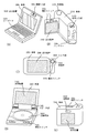
本発明を実施して作製されたアクティブマトリクス基板および液晶表示装置は様々な電気光学装置に用いることができる。そして、そのような電気光学装置を表示媒体として組み込んだ電子機器全てに本発明を適用することがでできる。電子機器としては、パーソナルコンピュータ、デジタルカメラ、ビデオカメラ、携帯情報端末(モバイルコンピュータ、携帯電話、電子書籍など)、ナビゲーションシステムなどが上げられる。それらの一例を図17に示す。
本実施形態では、実施形態1と同様なアクティブマトリクス基板で、エレクトロルミネッセンス(EL:Electro Luminescence)材料を用いた自発光型の表示パネル(以下、EL表示装置と記す)を作製する例について説明する。図18(A)はそのEL表示パネルの上面図を示す。図18(A)において、10は基板、11は画素部、12はソース側駆動回路、13はゲート側駆動回路であり、それぞれの駆動回路は配線14〜16を経てFPC17に至り、外部機器へと接続される。
や絶縁膜28のエッチング時(自発光層形成前の開口部の形成時)に形成しておけば良い。また、絶縁膜28をエッチングする際に、層間絶縁膜26まで一括でエッチングしても良い。この場合、層間絶縁膜26と絶縁膜28が同じ樹脂材料であれば、コンタクトホールの形状を良好なものとすることができる。
従って、発光の利用効率が非常に高く、明るい画像表示が可能となる。
本実施形態では、図20(B)に示した回路図とは異なる構造の画素とした場合の例について図21に示す。なお、本実施例において、2701はスイッチング用TFT2702のソース配線、2703はスイッチング用TFT2702のゲート配線、2704は電流制御用TFT、2705はコンデンサ、2706、2708は電流供給線、2707はEL素子とする。

は立ち下がり波形を示している。入力部と末端部の間隔は83mmである。図25においてJ2と表記された特性はTaN膜とTa膜を積層してゲート配線を形成し、J4と表記されたサンプルはAl−Nd膜でゲート配線を形成したサンプルである。ゲート配線の幅は10μmである。前者のサンプルでは入力部と末端部の立ち上がりおよび立ち下がり時間に大きな差があるのに対し、後者のサンプルではその差が非常に小さくなっている。表3に遅延時間についてまとめた結果を示す。J2サンプルの遅延時間はJ4サンプルの約十倍であり、表1で示すシート抵抗値から見て明らかなように、配線材料の抵抗が影響していると判断することができる。
102 下地膜
103b 結晶質半導体層
104〜107島状半導体層
128〜131 ゲート電極、132 容量配線
128a〜132a 導電層(A)
128b〜132b 導電層(B)
128c〜132c 導電層(C)
147、148 ゲート配線、149容量配線
147a〜149a 導電層(D)
147b〜149b 導電層(E)
150 第1の層間絶縁膜
151〜154 ソース配線
155〜158 ドレイン電極
159 パッシベーション膜
160 第2の層間絶縁膜
161、162 画素電極
Claims (7)
- 同一基板上に表示領域と、前記表示領域の周辺に設けられた駆動回路と、を有し、
前記表示領域は、第1の薄膜トランジスタを有し、
前記駆動回路は、第2の薄膜トランジスタを有し、
前記第1の薄膜トランジスタと前記第2の薄膜トランジスタは、リンがドープされたシリコンでなるゲート電極を有し、
前記ゲート電極は、チャネル形成領域の外側に設けられた接続部でアルミニウムまたは銅を主成分とする層とタンタル、タングステン、チタン、モリブデンから選ばれた少なくとも1種を主成分とする層とを有する配線と電気的に接続することを特徴とする液晶表示装置。 - 請求項1において、
前記ゲート電極は、前記配線のアルミニウムまたは銅を主成分とする層とは直接接触しないことを特徴とする液晶表示装置。 - 請求項1または2において、
前記配線は、チタン膜、チタンを含むアルミニウム膜、チタン膜を順に積層した三層構造であることを特徴とする液晶表示装置。 - 同一基板上に表示領域と、前記表示領域の周辺に設けられた駆動回路と、を有し、
前記表示領域は、nチャネル型の第1の薄膜トランジスタを有し、
前記駆動回路は、nチャネル型の第2の薄膜トランジスタを有し、
前記第1の薄膜トランジスタと前記第2の薄膜トランジスタは、タンタル、タングステン、チタン、モリブデンから選ばれた少なくとも1種を主成分とする導電層でなるゲート電極を有し、
前記ゲート電極は、チャネル形成領域の外側に設けられた接続部でアルミニウムまたは銅を主成分とする層とタンタル、タングステン、チタン、モリブデンから選ばれた少なくとも1種を主成分とする層とを有する配線と電気的に接続することを特徴とする液晶表示装置。 - 請求項1乃至4のいずれか一において、
前記第1の薄膜トランジスタが有する半導体層のLDD領域は、前記第1の薄膜トランジスタのゲート電極と重ならないように配置され、
前記第2の薄膜トランジスタが有する半導体層のLDD領域は、前記第2の薄膜トランジスタのゲート電極と重なるように配置されていることを特徴とする液晶表示装置。 - 請求項1乃至5のいずれか一において、前記第2の薄膜トランジスタは、シフトレジスタ回路、レベルシフタ回路又はバッファ回路に用いられていることを特徴とする液晶表示装置。
- 請求項1乃至7のいずれか一に記載の液晶表示装置を用いた携帯情報端末。
Priority Applications (1)
| Application Number | Priority Date | Filing Date | Title |
|---|---|---|---|
| JP2010116256A JP2010219549A (ja) | 1999-04-12 | 2010-05-20 | 液晶表示装置 |
Applications Claiming Priority (2)
| Application Number | Priority Date | Filing Date | Title |
|---|---|---|---|
| JP10464699 | 1999-04-12 | ||
| JP2010116256A JP2010219549A (ja) | 1999-04-12 | 2010-05-20 | 液晶表示装置 |
Related Parent Applications (1)
| Application Number | Title | Priority Date | Filing Date |
|---|---|---|---|
| JP2000110445A Division JP4536202B2 (ja) | 1999-04-12 | 2000-04-12 | 半導体装置およびその作製方法、並びに電子機器 |
Related Child Applications (1)
| Application Number | Title | Priority Date | Filing Date |
|---|---|---|---|
| JP2011085976A Division JP5433618B2 (ja) | 1999-04-12 | 2011-04-08 | 半導体装置 |
Publications (1)
| Publication Number | Publication Date |
|---|---|
| JP2010219549A true JP2010219549A (ja) | 2010-09-30 |
Family
ID=14386237
Family Applications (8)
| Application Number | Title | Priority Date | Filing Date |
|---|---|---|---|
| JP2010116256A Withdrawn JP2010219549A (ja) | 1999-04-12 | 2010-05-20 | 液晶表示装置 |
| JP2011085976A Expired - Lifetime JP5433618B2 (ja) | 1999-04-12 | 2011-04-08 | 半導体装置 |
| JP2012276399A Expired - Lifetime JP5674754B2 (ja) | 1999-04-12 | 2012-12-19 | 表示装置 |
| JP2013097406A Withdrawn JP2013201441A (ja) | 1999-04-12 | 2013-05-07 | 半導体装置 |
| JP2014176904A Expired - Lifetime JP6130339B2 (ja) | 1999-04-12 | 2014-09-01 | El表示装置 |
| JP2015211686A Expired - Lifetime JP6022016B2 (ja) | 1999-04-12 | 2015-10-28 | El表示装置 |
| JP2016193261A Withdrawn JP2017016154A (ja) | 1999-04-12 | 2016-09-30 | 表示装置 |
| JP2018024697A Expired - Lifetime JP6563051B2 (ja) | 1999-04-12 | 2018-02-15 | 表示装置 |
Family Applications After (7)
| Application Number | Title | Priority Date | Filing Date |
|---|---|---|---|
| JP2011085976A Expired - Lifetime JP5433618B2 (ja) | 1999-04-12 | 2011-04-08 | 半導体装置 |
| JP2012276399A Expired - Lifetime JP5674754B2 (ja) | 1999-04-12 | 2012-12-19 | 表示装置 |
| JP2013097406A Withdrawn JP2013201441A (ja) | 1999-04-12 | 2013-05-07 | 半導体装置 |
| JP2014176904A Expired - Lifetime JP6130339B2 (ja) | 1999-04-12 | 2014-09-01 | El表示装置 |
| JP2015211686A Expired - Lifetime JP6022016B2 (ja) | 1999-04-12 | 2015-10-28 | El表示装置 |
| JP2016193261A Withdrawn JP2017016154A (ja) | 1999-04-12 | 2016-09-30 | 表示装置 |
| JP2018024697A Expired - Lifetime JP6563051B2 (ja) | 1999-04-12 | 2018-02-15 | 表示装置 |
Country Status (6)
| Country | Link |
|---|---|
| US (5) | US7456430B1 (ja) |
| EP (4) | EP1780589A3 (ja) |
| JP (8) | JP2010219549A (ja) |
| KR (1) | KR100733892B1 (ja) |
| CN (4) | CN1197157C (ja) |
| TW (1) | TW444257B (ja) |
Families Citing this family (43)
| Publication number | Priority date | Publication date | Assignee | Title |
|---|---|---|---|---|
| EP2284605A3 (en) * | 1999-02-23 | 2017-10-18 | Semiconductor Energy Laboratory Co, Ltd. | Semiconductor device and fabrication method thereof |
| US6531713B1 (en) * | 1999-03-19 | 2003-03-11 | Semiconductor Energy Laboratory Co., Ltd. | Electro-optical device and manufacturing method thereof |
| TW444257B (en) | 1999-04-12 | 2001-07-01 | Semiconductor Energy Lab | Semiconductor device and method for fabricating the same |
| EP1049167A3 (en) | 1999-04-30 | 2007-10-24 | Sel Semiconductor Energy Laboratory Co., Ltd. | Semiconductor device and manufacturing method thereof |
| JP4666723B2 (ja) | 1999-07-06 | 2011-04-06 | 株式会社半導体エネルギー研究所 | 半導体装置の作製方法 |
| SG116443A1 (en) | 2001-03-27 | 2005-11-28 | Semiconductor Energy Lab | Wiring and method of manufacturing the same, and wiring board and method of manufacturing the same. |
| KR100507278B1 (ko) * | 2001-05-31 | 2005-08-09 | 비오이 하이디스 테크놀로지 주식회사 | 박막 트랜지스터 액정표시장치 제조방법 |
| TWI338366B (en) | 2002-09-20 | 2011-03-01 | Semiconductor Energy Lab | Display device and manufacturing method thereof |
| KR100493030B1 (ko) * | 2002-11-08 | 2005-06-07 | 삼성전자주식회사 | 하드 디스크 드라이브의 액츄에이터 로킹 장치 |
| JP4906051B2 (ja) | 2002-12-19 | 2012-03-28 | 株式会社半導体エネルギー研究所 | 表示装置 |
| CN101819984B (zh) * | 2003-01-24 | 2014-04-30 | 株式会社半导体能源研究所 | 电子书 |
| US7221095B2 (en) | 2003-06-16 | 2007-05-22 | Semiconductor Energy Laboratory Co., Ltd. | Light emitting device and method for fabricating light emitting device |
| US7161184B2 (en) | 2003-06-16 | 2007-01-09 | Semiconductor Energy Laboratory Co., Ltd. | Display device and method for manufacturing the same |
| US7224118B2 (en) | 2003-06-17 | 2007-05-29 | Semiconductor Energy Laboratory Co., Ltd. | Display device and electronic apparatus having a wiring connected to a counter electrode via an opening portion in an insulating layer that surrounds a pixel electrode |
| SG142140A1 (en) | 2003-06-27 | 2008-05-28 | Semiconductor Energy Lab | Display device and method of manufacturing thereof |
| US20070052021A1 (en) * | 2005-08-23 | 2007-03-08 | Semiconductor Energy Laboratory Co., Ltd. | Transistor, and display device, electronic device, and semiconductor device using the same |
| KR101117948B1 (ko) | 2005-11-15 | 2012-02-15 | 가부시키가이샤 한도오따이 에네루기 켄큐쇼 | 액정 디스플레이 장치 제조 방법 |
| US7851996B2 (en) * | 2005-11-16 | 2010-12-14 | Canon Kabushiki Kaisha | Display apparatus |
| US8395746B2 (en) * | 2006-01-31 | 2013-03-12 | Semiconductor Energy Laboratory Co., Ltd. | Display device |
| JP4321557B2 (ja) * | 2006-07-06 | 2009-08-26 | エプソンイメージングデバイス株式会社 | 電気光学装置、電気光学装置の製造方法及び電子機器 |
| JP4991634B2 (ja) * | 2008-06-09 | 2012-08-01 | キヤノン株式会社 | 有機el発光装置 |
| KR101652693B1 (ko) | 2008-10-03 | 2016-09-01 | 가부시키가이샤 한도오따이 에네루기 켄큐쇼 | 표시 장치 |
| JP5577646B2 (ja) * | 2009-01-09 | 2014-08-27 | セイコーエプソン株式会社 | 電気泳動表示装置、電子機器、電気泳動表示装置の製造方法 |
| US20100224878A1 (en) | 2009-03-05 | 2010-09-09 | Semiconductor Energy Laboratory Co., Ltd. | Semiconductor device |
| US8461582B2 (en) | 2009-03-05 | 2013-06-11 | Semiconductor Energy Laboratory Co., Ltd. | Semiconductor device and method for manufacturing the same |
| CN103426935A (zh) | 2009-11-27 | 2013-12-04 | 株式会社半导体能源研究所 | 半导体装置和及其制造方法 |
| US8415677B2 (en) * | 2010-01-20 | 2013-04-09 | International Business Machines Corporation | Field-effect transistor device having a metal gate stack with an oxygen barrier layer |
| US8304840B2 (en) * | 2010-07-29 | 2012-11-06 | Taiwan Semiconductor Manufacturing Company, Ltd. | Spacer structures of a semiconductor device |
| WO2012042564A1 (ja) | 2010-09-29 | 2012-04-05 | パナソニック株式会社 | 表示装置用薄膜半導体装置、表示装置用薄膜半導体装置の製造方法、el表示パネル及びel表示装置 |
| JP5386643B2 (ja) | 2010-09-29 | 2014-01-15 | パナソニック株式会社 | 表示装置用薄膜半導体装置、表示装置用薄膜半導体装置の製造方法、el表示パネル及びel表示装置 |
| US9508904B2 (en) * | 2011-01-31 | 2016-11-29 | Cree, Inc. | Structures and substrates for mounting optical elements and methods and devices for providing the same background |
| JP5626010B2 (ja) | 2011-02-25 | 2014-11-19 | 富士通株式会社 | 半導体装置及びその製造方法、電源装置 |
| TW201322341A (zh) * | 2011-11-21 | 2013-06-01 | Ind Tech Res Inst | 半導體元件以及其製造方法 |
| TWI491050B (zh) * | 2011-11-25 | 2015-07-01 | Sony Corp | 電晶體,顯示器及電子裝置 |
| TWI611567B (zh) * | 2013-02-27 | 2018-01-11 | 半導體能源研究所股份有限公司 | 半導體裝置、驅動電路及顯示裝置 |
| KR102086422B1 (ko) | 2013-03-28 | 2020-03-10 | 삼성디스플레이 주식회사 | 표시패널 및 이의 제조방법 |
| JP6867737B2 (ja) * | 2016-08-30 | 2021-05-12 | ソニーセミコンダクタソリューションズ株式会社 | 表示装置及び電子機器 |
| CN107134474B (zh) * | 2017-06-12 | 2020-07-24 | 武汉华星光电半导体显示技术有限公司 | 薄膜晶体管及其制作方法、有机电致发光显示器 |
| US11049887B2 (en) | 2017-11-10 | 2021-06-29 | Applied Materials, Inc. | Layer stack for display applications |
| US10692799B2 (en) * | 2018-06-01 | 2020-06-23 | Innolux Corporation | Semiconductor electronic device |
| KR102600041B1 (ko) * | 2018-06-07 | 2023-11-08 | 삼성디스플레이 주식회사 | 유기 발광 표시 장치 |
| CN109686861B (zh) * | 2018-12-26 | 2020-12-11 | 上海晶合光电科技有限公司 | 一种环套式分立控制图案化有机电致发光器件及其制备方法 |
| JP2023144395A (ja) * | 2022-03-28 | 2023-10-11 | セイコーエプソン株式会社 | 電気光学装置および電子機器 |
Citations (2)
| Publication number | Priority date | Publication date | Assignee | Title |
|---|---|---|---|---|
| JPH07111334A (ja) * | 1993-08-20 | 1995-04-25 | Semiconductor Energy Lab Co Ltd | 半導体装置およびその作製方法 |
| JPH10326899A (ja) * | 1997-05-23 | 1998-12-08 | Semiconductor Energy Lab Co Ltd | 半導体デバイス及びその作製方法及び半導体装置 |
Family Cites Families (134)
| Publication number | Priority date | Publication date | Assignee | Title |
|---|---|---|---|---|
| US699543A (en) * | 1896-06-03 | 1902-05-06 | Electric Vehicle Company | Motor-vehicle. |
| US679749A (en) * | 1901-03-12 | 1901-08-06 | Louis J Hirt | Coke-oven. |
| US710910A (en) * | 1902-01-09 | 1902-10-07 | John H Wescott | Compound engine. |
| JP3437863B2 (ja) * | 1993-01-18 | 2003-08-18 | 株式会社半導体エネルギー研究所 | Mis型半導体装置の作製方法 |
| JPS5847461A (ja) | 1981-09-16 | 1983-03-19 | Takeda Chem Ind Ltd | 高比容化学調味料顆粒およびその製造法 |
| JPH0613612Y2 (ja) | 1983-07-20 | 1994-04-13 | ヤンマー農機株式会社 | 作業機の角度制御装置 |
| JPS6096921A (ja) | 1983-10-31 | 1985-05-30 | Yamatake Honeywell Co Ltd | 電子スイツチの過電流検出回路 |
| JPH0613605Y2 (ja) | 1986-03-03 | 1994-04-13 | 大介 藤井 | 整畦機 |
| JPH0194664A (ja) * | 1987-10-05 | 1989-04-13 | Nec Corp | 電界効果トランジスタ |
| JPH0827465B2 (ja) * | 1988-04-06 | 1996-03-21 | 株式会社日立製作所 | 平面デイスプレイ |
| JPH01281434A (ja) * | 1988-05-09 | 1989-11-13 | Toshiba Corp | 表示装置の電極形成方法 |
| JP2720470B2 (ja) * | 1988-08-26 | 1998-03-04 | 富士通株式会社 | 薄膜トランジスタマトリクスの製造方法 |
| JPH06104433B2 (ja) | 1988-11-04 | 1994-12-21 | 株式会社小糸製作所 | 車輌用コーナリングランプシステム |
| JPH07113726B2 (ja) * | 1989-01-10 | 1995-12-06 | 富士通株式会社 | 薄膜トランジスタマトリクスの製造方法 |
| JPH065852Y2 (ja) | 1989-02-10 | 1994-02-16 | 駿河精機株式会社 | 発泡プラスチックの減容機 |
| GB8909011D0 (en) | 1989-04-20 | 1989-06-07 | Friend Richard H | Electroluminescent devices |
| US5245207A (en) | 1989-04-21 | 1993-09-14 | Nobuo Mikoshiba | Integrated circuit |
| US5153690A (en) * | 1989-10-18 | 1992-10-06 | Hitachi, Ltd. | Thin-film device |
| US5266825A (en) * | 1989-10-18 | 1993-11-30 | Hitachi, Ltd. | Thin-film device |
| DE69032893T2 (de) * | 1989-11-30 | 1999-07-22 | Kabushiki Kaisha Toshiba, Kawasaki, Kanagawa | Werkstoff für elektrische Leiter, Elektronikagerät welches diesen verwendet und Flüssig-Kristall-Anzeige |
| JP3024620B2 (ja) | 1990-04-11 | 2000-03-21 | セイコーエプソン株式会社 | 液晶パネルの製造方法 |
| GB2243948B (en) | 1990-04-20 | 1994-06-08 | Nobuo Mikoshiba | Integrated circuit |
| JP2628928B2 (ja) | 1990-05-22 | 1997-07-09 | 株式会社フロンテック | 薄膜トランジスタアレイおよびその製造方法 |
| US5402254B1 (en) * | 1990-10-17 | 1998-09-22 | Hitachi Ltd | Liquid crystal display device with tfts in which pixel electrodes are formed in the same plane as the gate electrodes with anodized oxide films before the deposition of silicon |
| US5343063A (en) * | 1990-12-18 | 1994-08-30 | Sundisk Corporation | Dense vertical programmable read only memory cell structure and processes for making them |
| JPH04364723A (ja) * | 1991-06-12 | 1992-12-17 | Kawasaki Steel Corp | 半導体装置及びその製造方法 |
| JPH07111334B2 (ja) | 1991-07-15 | 1995-11-29 | 協同組合ブライト北九州 | 表面形状測定装置 |
| JPH0613612A (ja) * | 1991-12-03 | 1994-01-21 | Nec Corp | 薄膜トランジスタ |
| JPH05326960A (ja) * | 1992-05-20 | 1993-12-10 | Seiko Epson Corp | 薄膜トランジスタを備えた固体装置およびその製造方法 |
| JPH065852A (ja) * | 1992-06-23 | 1994-01-14 | Oki Electric Ind Co Ltd | Mosfet及びその製造方法 |
| WO1994000882A1 (fr) | 1992-06-24 | 1994-01-06 | Seiko Epson Corporation | Transistor a couches minces, dispositif a semi-conducteurs, dispositif d'affichage et procede de fabrication d'un transistor a couches minces |
| JP3189399B2 (ja) | 1992-06-26 | 2001-07-16 | ソニー株式会社 | 半導体装置の製造方法 |
| EP0582486A2 (en) | 1992-08-07 | 1994-02-09 | Sharp Kabushiki Kaisha | A thin film transistor pair and a process for fabricating the same |
| JP2859784B2 (ja) | 1992-09-03 | 1999-02-24 | シャープ株式会社 | アクティブマトリクス基板 |
| TW232751B (en) | 1992-10-09 | 1994-10-21 | Semiconductor Energy Res Co Ltd | Semiconductor device and method for forming the same |
| US6624477B1 (en) * | 1992-10-09 | 2003-09-23 | Semiconductor Energy Laboratory Co., Ltd. | Semiconductor device and method for manufacturing the same |
| US5576556A (en) * | 1993-08-20 | 1996-11-19 | Semiconductor Energy Laboratory Co., Ltd. | Thin film semiconductor device with gate metal oxide and sidewall spacer |
| JP3587537B2 (ja) * | 1992-12-09 | 2004-11-10 | 株式会社半導体エネルギー研究所 | 半導体装置 |
| JP3204764B2 (ja) * | 1992-12-28 | 2001-09-04 | 日立金属株式会社 | ロータリシート切断装置およびその製造方法 |
| US5583067A (en) * | 1993-01-22 | 1996-12-10 | Intel Corporation | Inverse T-gate semiconductor device with self-aligned punchthrough stops and method of fabrication |
| JPH06260499A (ja) | 1993-03-02 | 1994-09-16 | Casio Comput Co Ltd | 薄膜トランジスタおよびその製造方法 |
| US6150692A (en) * | 1993-07-13 | 2000-11-21 | Sony Corporation | Thin film semiconductor device for active matrix panel |
| JP2789293B2 (ja) * | 1993-07-14 | 1998-08-20 | 株式会社半導体エネルギー研究所 | 半導体装置作製方法 |
| US5594569A (en) | 1993-07-22 | 1997-01-14 | Semiconductor Energy Laboratory Co., Ltd. | Liquid-crystal electro-optical apparatus and method of manufacturing the same |
| JP3212060B2 (ja) | 1993-09-20 | 2001-09-25 | 株式会社半導体エネルギー研究所 | 半導体装置およびその作製方法 |
| TW297142B (ja) * | 1993-09-20 | 1997-02-01 | Handotai Energy Kenkyusho Kk | |
| US5719065A (en) * | 1993-10-01 | 1998-02-17 | Semiconductor Energy Laboratory Co., Ltd. | Method for manufacturing semiconductor device with removable spacers |
| JP2821347B2 (ja) * | 1993-10-12 | 1998-11-05 | 日本電気株式会社 | 電流制御型発光素子アレイ |
| US5923962A (en) | 1993-10-29 | 1999-07-13 | Semiconductor Energy Laboratory Co., Ltd. | Method for manufacturing a semiconductor device |
| TW264575B (ja) | 1993-10-29 | 1995-12-01 | Handotai Energy Kenkyusho Kk | |
| JP3431033B2 (ja) | 1993-10-29 | 2003-07-28 | 株式会社半導体エネルギー研究所 | 半導体作製方法 |
| EP0735152B1 (en) * | 1993-12-14 | 2002-04-17 | Kabushiki Kaisha Toshiba | Molybdenum-tungsten material for wiring, molybdenum-tungsten target for wiring, process for producing the same, and molybdenum-tungsten wiring thin film |
| JPH07263705A (ja) | 1994-03-24 | 1995-10-13 | Sony Corp | 薄膜トランジスタ |
| DE19500380C2 (de) * | 1994-05-20 | 2001-05-17 | Mitsubishi Electric Corp | Aktivmatrix-Flüssigkristallanzeige und Herstellungsverfahren dafür |
| JPH07318975A (ja) | 1994-05-25 | 1995-12-08 | Sanyo Electric Co Ltd | 液晶表示装置 |
| JP3281756B2 (ja) | 1994-05-31 | 2002-05-13 | 三洋電機株式会社 | 半導体装置及びそれを用いた液晶パネル |
| JP3232343B2 (ja) * | 1994-05-31 | 2001-11-26 | 日本電信電話株式会社 | 横形mos電界効果トランジスタ |
| US5834827A (en) * | 1994-06-15 | 1998-11-10 | Seiko Epson Corporation | Thin film semiconductor device, fabrication method thereof, electronic device and its fabrication method |
| JP3072000B2 (ja) * | 1994-06-23 | 2000-07-31 | 株式会社半導体エネルギー研究所 | 半導体装置の作製方法 |
| JP2692590B2 (ja) * | 1994-06-29 | 1997-12-17 | 日本電気株式会社 | 半導体装置およびその製造方法 |
| KR960009013A (ko) | 1994-08-18 | 1996-03-22 | 김광호 | 타이타늄 나이트라이드(TiN) 게이트전극 형성방법 |
| JPH0864838A (ja) | 1994-08-26 | 1996-03-08 | Casio Comput Co Ltd | 薄膜トランジスタ |
| KR100213402B1 (ko) | 1994-09-29 | 1999-08-02 | 니시무로 타이죠 | 전극배선재료 및 이를 이용한 전극배선기판 |
| JP3488551B2 (ja) | 1994-09-29 | 2004-01-19 | 株式会社東芝 | 電極配線材料およびこれを用いた電極配線基板 |
| JPH08125193A (ja) | 1994-10-20 | 1996-05-17 | Semiconductor Energy Lab Co Ltd | 半導体集積回路とその作製方法 |
| AU4290396A (en) | 1994-11-30 | 1996-06-19 | Micron Technology, Inc. | A method of depositing tungsten nitride using a source gas comprising silicon |
| US5550066A (en) * | 1994-12-14 | 1996-08-27 | Eastman Kodak Company | Method of fabricating a TFT-EL pixel |
| JPH08179362A (ja) | 1994-12-22 | 1996-07-12 | Mitsubishi Electric Corp | 薄膜トランジスタアレイ基板 |
| JPH08274336A (ja) * | 1995-03-30 | 1996-10-18 | Toshiba Corp | 多結晶半導体薄膜トランジスタ及びその製造方法 |
| KR960039434A (ko) | 1995-04-21 | 1996-11-25 | 김광호 | 금속 게이트 전극을 갖는 트랜지스터 및 그 제조방법 |
| JP3501874B2 (ja) | 1995-05-24 | 2004-03-02 | 株式会社半導体エネルギー研究所 | 金属配線の作製方法 |
| JPH0926600A (ja) | 1995-07-13 | 1997-01-28 | Sanyo Electric Co Ltd | 液晶表示装置 |
| JPH0945789A (ja) | 1995-07-27 | 1997-02-14 | Hitachi Ltd | 半導体装置およびその製造方法 |
| KR0156202B1 (ko) | 1995-08-22 | 1998-11-16 | 구자홍 | 액정표시장치 및 그 제조방법 |
| WO1997008752A1 (en) | 1995-08-25 | 1997-03-06 | Hitachi, Ltd. | Mis semiconductor device |
| JP3369811B2 (ja) | 1995-09-13 | 2003-01-20 | 株式会社東芝 | 半導体装置、およびその製造方法 |
| JPH09153623A (ja) | 1995-11-30 | 1997-06-10 | Sony Corp | 薄膜半導体装置 |
| JP3239202B2 (ja) * | 1995-12-01 | 2001-12-17 | シャープ株式会社 | Mosトランジスタ及びその製造方法 |
| JP2865039B2 (ja) * | 1995-12-26 | 1999-03-08 | 日本電気株式会社 | 薄膜トランジスタ基板の製造方法 |
| US5888858A (en) * | 1996-01-20 | 1999-03-30 | Semiconductor Energy Laboratory Co., Ltd. | Semiconductor device and fabrication method thereof |
| JPH09260629A (ja) * | 1996-03-26 | 1997-10-03 | Sony Corp | 増幅型固体撮像素子の製造方法 |
| KR100193987B1 (ko) * | 1996-05-11 | 1999-06-15 | 구자홍 | 구동회로 일체형 액정표시소자 및 제조방법 |
| JPH09325358A (ja) * | 1996-06-04 | 1997-12-16 | Sharp Corp | 液晶表示装置およびその製造方法 |
| KR100207472B1 (ko) | 1996-06-07 | 1999-07-15 | 윤종용 | 티타늄 질화막 적층 구조의 게이트 전극을 갖춘 반도체장치 및 그 제조 방법 |
| US5721163A (en) * | 1996-06-10 | 1998-02-24 | Chartered Semiconductor Manufacturing Pte, Ltd. | Method of manufacture of thin film transistor SRAM device with a titanium nitride or silicide gate |
| KR100209620B1 (ko) | 1996-08-31 | 1999-07-15 | 구자홍 | 액정 표시 장치 및 그 제조방법 |
| US6542137B2 (en) * | 1996-09-26 | 2003-04-01 | Seiko Epson Corporation | Display device |
| JP4032443B2 (ja) | 1996-10-09 | 2008-01-16 | セイコーエプソン株式会社 | 薄膜トランジスタ、回路、アクティブマトリクス基板、液晶表示装置 |
| JPH10135462A (ja) | 1996-10-28 | 1998-05-22 | Matsushita Electric Ind Co Ltd | 薄膜トランジスタ |
| JP3457819B2 (ja) * | 1996-11-28 | 2003-10-20 | カシオ計算機株式会社 | 表示装置 |
| JP2988399B2 (ja) * | 1996-11-28 | 1999-12-13 | 日本電気株式会社 | アクティブマトリクス基板 |
| JP3463971B2 (ja) * | 1996-12-26 | 2003-11-05 | 出光興産株式会社 | 有機アクティブel発光装置 |
| JPH10319872A (ja) * | 1997-01-17 | 1998-12-04 | Xerox Corp | アクティブマトリクス有機発光ダイオード表示装置 |
| JP3864476B2 (ja) * | 1997-01-24 | 2006-12-27 | ソニー株式会社 | 薄膜半導体装置 |
| JPH10319909A (ja) * | 1997-05-22 | 1998-12-04 | Casio Comput Co Ltd | 表示装置及びその駆動方法 |
| JPH10233505A (ja) | 1997-02-21 | 1998-09-02 | Hitachi Ltd | 半導体装置の製造方法 |
| JPH10335334A (ja) * | 1997-03-31 | 1998-12-18 | Seiko Epson Corp | 半導体装置及びその製造方法、並びに液晶装置 |
| JP3346217B2 (ja) * | 1997-04-04 | 2002-11-18 | カシオ計算機株式会社 | 配線の形成方法および表示装置の製造方法 |
| JPH10319431A (ja) | 1997-05-15 | 1998-12-04 | Advanced Display:Kk | 薄膜トランジスタアレイ基板 |
| JPH10325963A (ja) | 1997-05-26 | 1998-12-08 | Sharp Corp | アクティブマトリクス型表示装置の製造方法 |
| JP3541625B2 (ja) * | 1997-07-02 | 2004-07-14 | セイコーエプソン株式会社 | 表示装置及びアクティブマトリクス基板 |
| JP3830238B2 (ja) * | 1997-08-29 | 2006-10-04 | セイコーエプソン株式会社 | アクティブマトリクス型装置 |
| JP4159633B2 (ja) | 1997-09-19 | 2008-10-01 | 株式会社半導体エネルギー研究所 | 半導体装置およびその作製方法並びに電子機器 |
| JPH1197707A (ja) | 1997-09-24 | 1999-04-09 | Semiconductor Energy Lab Co Ltd | 半導体装置の作製方法 |
| US6218219B1 (en) * | 1997-09-29 | 2001-04-17 | Semiconductor Energy Laboratory Co., Ltd. | Semiconductor device and fabrication method thereof |
| JP3523093B2 (ja) | 1997-11-28 | 2004-04-26 | 株式会社東芝 | 半導体装置およびその製造方法 |
| JPH11194366A (ja) | 1998-01-07 | 1999-07-21 | Seiko Epson Corp | アクティブマトリックス基板およびその製造方法、液晶装置および電子機器 |
| JP4115586B2 (ja) * | 1998-03-27 | 2008-07-09 | 株式会社半導体エネルギー研究所 | 半導体装置の作製方法 |
| US6482684B1 (en) * | 1998-03-27 | 2002-11-19 | Semiconductor Energy Laboratory Co., Ltd. | Method of manufacturing a TFT with Ge seeded amorphous Si layer |
| US6225168B1 (en) * | 1998-06-04 | 2001-05-01 | Advanced Micro Devices, Inc. | Semiconductor device having metal gate electrode and titanium or tantalum nitride gate dielectric barrier layer and process of fabrication thereof |
| JP2000082817A (ja) | 1998-09-04 | 2000-03-21 | Sharp Corp | アクティブマトリクス基板及びその製造方法 |
| JP2000111945A (ja) * | 1998-10-01 | 2000-04-21 | Sony Corp | 電気光学装置、電気光学装置用の駆動基板、及びこれらの製造方法 |
| US6420758B1 (en) * | 1998-11-17 | 2002-07-16 | Semiconductor Energy Laboratory Co., Ltd. | Semiconductor device having an impurity region overlapping a gate electrode |
| CN1213390C (zh) | 1998-11-26 | 2005-08-03 | 精工爱普生株式会社 | 电光装置及其制造方法和电子装置 |
| US6420988B1 (en) * | 1998-12-03 | 2002-07-16 | Semiconductor Energy Laboratory Co., Ltd. | Digital analog converter and electronic device using the same |
| US6259138B1 (en) * | 1998-12-18 | 2001-07-10 | Semiconductor Energy Laboratory Co., Ltd. | Semiconductor device having multilayered gate electrode and impurity regions overlapping therewith |
| US6469317B1 (en) * | 1998-12-18 | 2002-10-22 | Semiconductor Energy Laboratory Co., Ltd. | Semiconductor device and method of fabricating the same |
| US7612020B2 (en) * | 1998-12-28 | 2009-11-03 | Illumina, Inc. | Composite arrays utilizing microspheres with a hybridization chamber |
| US6593592B1 (en) * | 1999-01-29 | 2003-07-15 | Semiconductor Energy Laboratory Co., Ltd. | Semiconductor device having thin film transistors |
| US6777716B1 (en) * | 1999-02-12 | 2004-08-17 | Semiconductor Energy Laboratory Co., Ltd. | Semiconductor display device and method of manufacturing therefor |
| EP2284605A3 (en) | 1999-02-23 | 2017-10-18 | Semiconductor Energy Laboratory Co, Ltd. | Semiconductor device and fabrication method thereof |
| JP3399432B2 (ja) * | 1999-02-26 | 2003-04-21 | セイコーエプソン株式会社 | 電気光学装置の製造方法及び電気光学装置 |
| US6614083B1 (en) * | 1999-03-17 | 2003-09-02 | Semiconductor Energy Laboratory Co., Ltd. | Wiring material and a semiconductor device having wiring using the material, and the manufacturing method |
| US6531713B1 (en) | 1999-03-19 | 2003-03-11 | Semiconductor Energy Laboratory Co., Ltd. | Electro-optical device and manufacturing method thereof |
| US6399988B1 (en) | 1999-03-26 | 2002-06-04 | Semiconductor Energy Laboratory Co., Ltd. | Thin film transistor having lightly doped regions |
| TW469484B (en) | 1999-03-26 | 2001-12-21 | Semiconductor Energy Lab | A method for manufacturing an electrooptical device |
| JP4536202B2 (ja) * | 1999-04-12 | 2010-09-01 | 株式会社半導体エネルギー研究所 | 半導体装置およびその作製方法、並びに電子機器 |
| TW444257B (en) | 1999-04-12 | 2001-07-01 | Semiconductor Energy Lab | Semiconductor device and method for fabricating the same |
| EP1049167A3 (en) | 1999-04-30 | 2007-10-24 | Sel Semiconductor Energy Laboratory Co., Ltd. | Semiconductor device and manufacturing method thereof |
| US6661096B1 (en) | 1999-06-29 | 2003-12-09 | Semiconductor Energy Laboratory Co., Ltd. | Wiring material semiconductor device provided with a wiring using the wiring material and method of manufacturing thereof |
| US6171910B1 (en) | 1999-07-21 | 2001-01-09 | Motorola Inc. | Method for forming a semiconductor device |
| CA2402834A1 (en) | 2000-03-23 | 2001-09-27 | Immusol Incorporated | Brca-1 regulators and methods of use |
| CN1123465C (zh) * | 2000-04-18 | 2003-10-08 | 李博良 | 防追尾的载货车后部防护装置 |
| KR100846762B1 (ko) * | 2001-09-11 | 2008-07-16 | 삼성전자주식회사 | 키보드유닛의 키스위치 |
-
2000
- 2000-04-06 TW TW089106332A patent/TW444257B/zh not_active IP Right Cessation
- 2000-04-07 US US09/544,801 patent/US7456430B1/en not_active Expired - Fee Related
- 2000-04-08 KR KR1020000018404A patent/KR100733892B1/ko not_active IP Right Cessation
- 2000-04-11 EP EP07002101.9A patent/EP1780589A3/en not_active Withdrawn
- 2000-04-11 EP EP10009810A patent/EP2256817A2/en not_active Withdrawn
- 2000-04-11 EP EP00107789A patent/EP1045451A3/en not_active Withdrawn
- 2000-04-11 EP EP07002100A patent/EP1786037A3/en not_active Withdrawn
- 2000-04-12 CN CNB001188097A patent/CN1197157C/zh not_active Expired - Fee Related
- 2000-04-12 CN CN2005100081531A patent/CN1655038B/zh not_active Expired - Fee Related
- 2000-04-12 CN CN2006100737812A patent/CN1870293B/zh not_active Expired - Fee Related
- 2000-04-12 CN CNB2006101030029A patent/CN100481506C/zh not_active Expired - Fee Related
-
2006
- 2006-04-03 US US11/396,436 patent/US8129721B2/en not_active Expired - Fee Related
- 2006-07-14 US US11/487,010 patent/US7855380B2/en not_active Expired - Fee Related
-
2010
- 2010-05-20 JP JP2010116256A patent/JP2010219549A/ja not_active Withdrawn
- 2010-07-19 US US12/839,113 patent/US8071981B2/en not_active Expired - Fee Related
-
2011
- 2011-04-08 JP JP2011085976A patent/JP5433618B2/ja not_active Expired - Lifetime
-
2012
- 2012-03-05 US US13/411,842 patent/US8866143B2/en not_active Expired - Fee Related
- 2012-12-19 JP JP2012276399A patent/JP5674754B2/ja not_active Expired - Lifetime
-
2013
- 2013-05-07 JP JP2013097406A patent/JP2013201441A/ja not_active Withdrawn
-
2014
- 2014-09-01 JP JP2014176904A patent/JP6130339B2/ja not_active Expired - Lifetime
-
2015
- 2015-10-28 JP JP2015211686A patent/JP6022016B2/ja not_active Expired - Lifetime
-
2016
- 2016-09-30 JP JP2016193261A patent/JP2017016154A/ja not_active Withdrawn
-
2018
- 2018-02-15 JP JP2018024697A patent/JP6563051B2/ja not_active Expired - Lifetime
Patent Citations (2)
| Publication number | Priority date | Publication date | Assignee | Title |
|---|---|---|---|---|
| JPH07111334A (ja) * | 1993-08-20 | 1995-04-25 | Semiconductor Energy Lab Co Ltd | 半導体装置およびその作製方法 |
| JPH10326899A (ja) * | 1997-05-23 | 1998-12-08 | Semiconductor Energy Lab Co Ltd | 半導体デバイス及びその作製方法及び半導体装置 |
Also Published As
Similar Documents
| Publication | Publication Date | Title |
|---|---|---|
| JP6563051B2 (ja) | 表示装置 | |
| US6579736B2 (en) | Semiconductor device and method of manufacturing thereof | |
| JP4801238B2 (ja) | 半導体装置の作製方法 | |
| JP4536202B2 (ja) | 半導体装置およびその作製方法、並びに電子機器 | |
| JP4850326B2 (ja) | 半導体装置の作製方法 | |
| JP4527070B2 (ja) | 半導体装置およびその作製方法、並びに電子機器 | |
| JP4463377B2 (ja) | 半導体装置およびその作製方法 | |
| JP4527069B2 (ja) | 表示装置 | |
| JP2001053286A (ja) | 半導体膜およびその作製方法 | |
| KR100775130B1 (ko) | 반도체장치 | |
| KR100775129B1 (ko) | 반도체장치 | |
| JP4618842B2 (ja) | 半導体装置の作製方法 |
Legal Events
| Date | Code | Title | Description |
|---|---|---|---|
| A131 | Notification of reasons for refusal |
Free format text: JAPANESE INTERMEDIATE CODE: A131 Effective date: 20110322 |
|
| A521 | Request for written amendment filed |
Free format text: JAPANESE INTERMEDIATE CODE: A523 Effective date: 20110411 |
|
| A131 | Notification of reasons for refusal |
Free format text: JAPANESE INTERMEDIATE CODE: A131 Effective date: 20110712 |
|
| A521 | Request for written amendment filed |
Free format text: JAPANESE INTERMEDIATE CODE: A523 Effective date: 20110825 |
|
| A02 | Decision of refusal |
Free format text: JAPANESE INTERMEDIATE CODE: A02 Effective date: 20110920 |
|
| A521 | Request for written amendment filed |
Free format text: JAPANESE INTERMEDIATE CODE: A523 Effective date: 20111031 |
|
| A911 | Transfer to examiner for re-examination before appeal (zenchi) |
Free format text: JAPANESE INTERMEDIATE CODE: A911 Effective date: 20111121 |
|
| A912 | Re-examination (zenchi) completed and case transferred to appeal board |
Free format text: JAPANESE INTERMEDIATE CODE: A912 Effective date: 20111209 |
|
| A761 | Written withdrawal of application |
Free format text: JAPANESE INTERMEDIATE CODE: A761 Effective date: 20121204 |