JP4251129B2 - 実装構造体、電気光学装置及び電子機器 - Google Patents
実装構造体、電気光学装置及び電子機器 Download PDFInfo
- Publication number
- JP4251129B2 JP4251129B2 JP2004309131A JP2004309131A JP4251129B2 JP 4251129 B2 JP4251129 B2 JP 4251129B2 JP 2004309131 A JP2004309131 A JP 2004309131A JP 2004309131 A JP2004309131 A JP 2004309131A JP 4251129 B2 JP4251129 B2 JP 4251129B2
- Authority
- JP
- Japan
- Prior art keywords
- edge
- substrate
- wiring
- reinforcing member
- wirings
- Prior art date
- Legal status (The legal status is an assumption and is not a legal conclusion. Google has not performed a legal analysis and makes no representation as to the accuracy of the status listed.)
- Expired - Lifetime
Links
- 239000000758 substrate Substances 0.000 claims description 173
- 230000003014 reinforcing effect Effects 0.000 claims description 83
- 239000000463 material Substances 0.000 claims description 7
- 239000004973 liquid crystal related substance Substances 0.000 description 93
- 238000012986 modification Methods 0.000 description 20
- 230000004048 modification Effects 0.000 description 20
- 239000003566 sealing material Substances 0.000 description 5
- 239000010408 film Substances 0.000 description 3
- 230000010365 information processing Effects 0.000 description 3
- 238000004519 manufacturing process Methods 0.000 description 3
- 239000011159 matrix material Substances 0.000 description 3
- 238000000034 method Methods 0.000 description 3
- 238000013459 approach Methods 0.000 description 2
- 239000004020 conductor Substances 0.000 description 2
- 238000010586 diagram Methods 0.000 description 2
- 239000011521 glass Substances 0.000 description 2
- 238000002347 injection Methods 0.000 description 2
- 239000007924 injection Substances 0.000 description 2
- 239000011810 insulating material Substances 0.000 description 2
- 239000007788 liquid Substances 0.000 description 2
- 229920003217 poly(methylsilsesquioxane) Polymers 0.000 description 2
- 230000007261 regionalization Effects 0.000 description 2
- 230000002787 reinforcement Effects 0.000 description 2
- 229920003002 synthetic resin Polymers 0.000 description 2
- 239000000057 synthetic resin Substances 0.000 description 2
- 239000010409 thin film Substances 0.000 description 2
- 239000004743 Polypropylene Substances 0.000 description 1
- 239000000853 adhesive Substances 0.000 description 1
- 230000001070 adhesive effect Effects 0.000 description 1
- 230000003321 amplification Effects 0.000 description 1
- 238000005452 bending Methods 0.000 description 1
- 230000015572 biosynthetic process Effects 0.000 description 1
- 238000006243 chemical reaction Methods 0.000 description 1
- 239000000470 constituent Substances 0.000 description 1
- 238000012937 correction Methods 0.000 description 1
- 230000007423 decrease Effects 0.000 description 1
- 230000007547 defect Effects 0.000 description 1
- 238000005401 electroluminescence Methods 0.000 description 1
- 238000005516 engineering process Methods 0.000 description 1
- 239000003822 epoxy resin Substances 0.000 description 1
- 238000009863 impact test Methods 0.000 description 1
- 230000007246 mechanism Effects 0.000 description 1
- 239000002184 metal Substances 0.000 description 1
- 238000003199 nucleic acid amplification method Methods 0.000 description 1
- 230000003287 optical effect Effects 0.000 description 1
- 230000002093 peripheral effect Effects 0.000 description 1
- 239000012466 permeate Substances 0.000 description 1
- 238000000206 photolithography Methods 0.000 description 1
- 229920000647 polyepoxide Polymers 0.000 description 1
- 229920000728 polyester Polymers 0.000 description 1
- 229920001721 polyimide Polymers 0.000 description 1
- -1 polypropylene Polymers 0.000 description 1
- 229920001155 polypropylene Polymers 0.000 description 1
- 238000012545 processing Methods 0.000 description 1
- 229920005989 resin Polymers 0.000 description 1
- 239000011347 resin Substances 0.000 description 1
- 239000000565 sealant Substances 0.000 description 1
- 229920001187 thermosetting polymer Polymers 0.000 description 1
Images


Classifications
-
- H—ELECTRICITY
- H05—ELECTRIC TECHNIQUES NOT OTHERWISE PROVIDED FOR
- H05K—PRINTED CIRCUITS; CASINGS OR CONSTRUCTIONAL DETAILS OF ELECTRIC APPARATUS; MANUFACTURE OF ASSEMBLAGES OF ELECTRICAL COMPONENTS
- H05K3/00—Apparatus or processes for manufacturing printed circuits
- H05K3/36—Assembling printed circuits with other printed circuits
- H05K3/361—Assembling flexible printed circuits with other printed circuits
-
- G—PHYSICS
- G02—OPTICS
- G02F—OPTICAL DEVICES OR ARRANGEMENTS FOR THE CONTROL OF LIGHT BY MODIFICATION OF THE OPTICAL PROPERTIES OF THE MEDIA OF THE ELEMENTS INVOLVED THEREIN; NON-LINEAR OPTICS; FREQUENCY-CHANGING OF LIGHT; OPTICAL LOGIC ELEMENTS; OPTICAL ANALOGUE/DIGITAL CONVERTERS
- G02F1/00—Devices or arrangements for the control of the intensity, colour, phase, polarisation or direction of light arriving from an independent light source, e.g. switching, gating or modulating; Non-linear optics
- G02F1/01—Devices or arrangements for the control of the intensity, colour, phase, polarisation or direction of light arriving from an independent light source, e.g. switching, gating or modulating; Non-linear optics for the control of the intensity, phase, polarisation or colour
- G02F1/13—Devices or arrangements for the control of the intensity, colour, phase, polarisation or direction of light arriving from an independent light source, e.g. switching, gating or modulating; Non-linear optics for the control of the intensity, phase, polarisation or colour based on liquid crystals, e.g. single liquid crystal display cells
- G02F1/133—Constructional arrangements; Operation of liquid crystal cells; Circuit arrangements
- G02F1/1333—Constructional arrangements; Manufacturing methods
- G02F1/1345—Conductors connecting electrodes to cell terminals
- G02F1/13452—Conductors connecting driver circuitry and terminals of panels
-
- H—ELECTRICITY
- H05—ELECTRIC TECHNIQUES NOT OTHERWISE PROVIDED FOR
- H05K—PRINTED CIRCUITS; CASINGS OR CONSTRUCTIONAL DETAILS OF ELECTRIC APPARATUS; MANUFACTURE OF ASSEMBLAGES OF ELECTRICAL COMPONENTS
- H05K1/00—Printed circuits
- H05K1/02—Details
- H05K1/0277—Bendability or stretchability details
- H05K1/028—Bending or folding regions of flexible printed circuits
- H05K1/0281—Reinforcement details thereof
-
- G—PHYSICS
- G02—OPTICS
- G02F—OPTICAL DEVICES OR ARRANGEMENTS FOR THE CONTROL OF LIGHT BY MODIFICATION OF THE OPTICAL PROPERTIES OF THE MEDIA OF THE ELEMENTS INVOLVED THEREIN; NON-LINEAR OPTICS; FREQUENCY-CHANGING OF LIGHT; OPTICAL LOGIC ELEMENTS; OPTICAL ANALOGUE/DIGITAL CONVERTERS
- G02F1/00—Devices or arrangements for the control of the intensity, colour, phase, polarisation or direction of light arriving from an independent light source, e.g. switching, gating or modulating; Non-linear optics
- G02F1/01—Devices or arrangements for the control of the intensity, colour, phase, polarisation or direction of light arriving from an independent light source, e.g. switching, gating or modulating; Non-linear optics for the control of the intensity, phase, polarisation or colour
- G02F1/13—Devices or arrangements for the control of the intensity, colour, phase, polarisation or direction of light arriving from an independent light source, e.g. switching, gating or modulating; Non-linear optics for the control of the intensity, phase, polarisation or colour based on liquid crystals, e.g. single liquid crystal display cells
- G02F1/133—Constructional arrangements; Operation of liquid crystal cells; Circuit arrangements
- G02F1/1333—Constructional arrangements; Manufacturing methods
- G02F1/1345—Conductors connecting electrodes to cell terminals
- G02F1/13456—Cell terminals located on one side of the display only
-
- H—ELECTRICITY
- H05—ELECTRIC TECHNIQUES NOT OTHERWISE PROVIDED FOR
- H05K—PRINTED CIRCUITS; CASINGS OR CONSTRUCTIONAL DETAILS OF ELECTRIC APPARATUS; MANUFACTURE OF ASSEMBLAGES OF ELECTRICAL COMPONENTS
- H05K2201/00—Indexing scheme relating to printed circuits covered by H05K1/00
- H05K2201/05—Flexible printed circuits [FPCs]
- H05K2201/056—Folded around rigid support or component
-
- H—ELECTRICITY
- H05—ELECTRIC TECHNIQUES NOT OTHERWISE PROVIDED FOR
- H05K—PRINTED CIRCUITS; CASINGS OR CONSTRUCTIONAL DETAILS OF ELECTRIC APPARATUS; MANUFACTURE OF ASSEMBLAGES OF ELECTRICAL COMPONENTS
- H05K2201/00—Indexing scheme relating to printed circuits covered by H05K1/00
- H05K2201/09—Shape and layout
- H05K2201/09009—Substrate related
- H05K2201/09063—Holes or slots in insulating substrate not used for electrical connections
-
- H—ELECTRICITY
- H05—ELECTRIC TECHNIQUES NOT OTHERWISE PROVIDED FOR
- H05K—PRINTED CIRCUITS; CASINGS OR CONSTRUCTIONAL DETAILS OF ELECTRIC APPARATUS; MANUFACTURE OF ASSEMBLAGES OF ELECTRICAL COMPONENTS
- H05K2201/00—Indexing scheme relating to printed circuits covered by H05K1/00
- H05K2201/09—Shape and layout
- H05K2201/09209—Shape and layout details of conductors
- H05K2201/09654—Shape and layout details of conductors covering at least two types of conductors provided for in H05K2201/09218 - H05K2201/095
- H05K2201/09781—Dummy conductors, i.e. not used for normal transport of current; Dummy electrodes of components
-
- H—ELECTRICITY
- H05—ELECTRIC TECHNIQUES NOT OTHERWISE PROVIDED FOR
- H05K—PRINTED CIRCUITS; CASINGS OR CONSTRUCTIONAL DETAILS OF ELECTRIC APPARATUS; MANUFACTURE OF ASSEMBLAGES OF ELECTRICAL COMPONENTS
- H05K2201/00—Indexing scheme relating to printed circuits covered by H05K1/00
- H05K2201/10—Details of components or other objects attached to or integrated in a printed circuit board
- H05K2201/10007—Types of components
- H05K2201/10128—Display
-
- H—ELECTRICITY
- H05—ELECTRIC TECHNIQUES NOT OTHERWISE PROVIDED FOR
- H05K—PRINTED CIRCUITS; CASINGS OR CONSTRUCTIONAL DETAILS OF ELECTRIC APPARATUS; MANUFACTURE OF ASSEMBLAGES OF ELECTRICAL COMPONENTS
- H05K2201/00—Indexing scheme relating to printed circuits covered by H05K1/00
- H05K2201/20—Details of printed circuits not provided for in H05K2201/01 - H05K2201/10
- H05K2201/2009—Reinforced areas, e.g. for a specific part of a flexible printed circuit
Landscapes
- Physics & Mathematics (AREA)
- Nonlinear Science (AREA)
- Engineering & Computer Science (AREA)
- Microelectronics & Electronic Packaging (AREA)
- Optics & Photonics (AREA)
- General Physics & Mathematics (AREA)
- Crystallography & Structural Chemistry (AREA)
- Chemical & Material Sciences (AREA)
- Mathematical Physics (AREA)
- Manufacturing & Machinery (AREA)
- Devices For Indicating Variable Information By Combining Individual Elements (AREA)
- Liquid Crystal (AREA)
- Structure Of Printed Boards (AREA)
Description
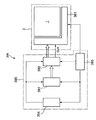
前記第1の補強部材は、前記端縁と前記第1の縁とが交差する部分と前記複数の第1の配線との間に設けられ、複数の前記第4の補強部材は、前記第2の縁と前記第1の開口端との間に設けられ、前記第1の補強部材と前記第4の補強部材は前記端縁に交差する方向に延在しており、複数の前記第4の補強部材の前記第1の開口端側端部は、前記第1の開口端に沿って配列していることを特徴とする。
本発明では、可撓性を有する第2の基板の第1の配線の破断を防止可能な実装構造体を備えているので、表示性能に優れた電気光学装置を得ることができる。
本発明の他の観点にかかる電子機器は、上述した電気光学装置を備えたことを特徴とする。
Claims (14)
- 端縁を有する基材と、該端縁と重なるように該基材に接続された可撓性基板と、を備えた実装構造体であって、
前記可撓性基板は、前記端縁と交差する複数の第1の配線と、第1の補強部材と、複数の第4の補強部材と、前記端縁に交差するように重なる第1の縁と、該第1の縁と交差するとともに前記基材と重なる第2の縁と、前記基材と重ならないように設けられた開口部と、を有し、
前記開口部は前記端縁に沿う方向に延在する第1の開口端を有し、
前記第1の補強部材は、前記端縁と前記第1の縁とが交差する部分と前記複数の第1の配線との間に設けられ、
複数の前記第4の補強部材は、前記第2の縁と前記第1の開口端との間に設けられ、
前記第1の補強部材と前記第4の補強部材は前記端縁に交差する方向に延在しており、
複数の前記第4の補強部材の前記第1の開口端側端部は、前記第1の開口端に沿って配列していることを特徴とする実装構造体。 - 前記第1の開口端は、前記端縁に対して前記第2の縁とは反対側に設けられており、
前記第4の補強部材は、前記端縁の前記第2の縁側から前記端縁の前記第1の開口端側まで延在していることを特徴とする請求項1に記載の実装構造体。 - 前記第4の補強部材は、前記端縁に対して略直交する方向に略直線的に延在していることを特徴とする請求項1または請求項2に記載の実装構造体。
- 前記開口部は、前記第1の開口端と前記第1の縁との間に、前記端縁に対して傾斜する第2の開口端をさらに有し、
複数の第5の補強部材が前記第4の補強部材と前記第1の配線との間に設けられ、
前記第5の補強部材は、前記端縁に対して略直交する方向に略直線的に延在し、
複数の前記第5の補強部材の前記第2の開口端側端部は、前記第2の開口端に沿って配列していることを特徴とする請求項1乃至3のうちいずれか一項に記載の実装構造体。 - 前記第1の補強部材は島形状のダミー配線であることを特徴とする請求項1乃至4のうちいずれか一項に記載の実装構造体。
- 前記第1の補強部材は、複数設けられており、少なくとも一つの第1の補強部材は、前記端縁に沿う方向の幅が他の第1の補強部材の幅と異なっていることを特徴とする請求項1から請求項4のうちのいずれか一項に記載の実装構造体。
- 前記基材は、表示装置を支持する枠体であることを特徴とする請求項1乃至6に記載の実装構造体。
- 前記基材は、配線を備えた基板であることを特徴とする請求項1乃至6に記載の実装構造体。
- 前記基材は前記第1の補強部材に接続される第1の端子を有し、
前記第1の補強部材は、前記第1の端子に接続される第2の端子を有するダミー配線であり、該第2の端子から延長して形成されていることを特徴とする請求項8に記載の実装構造体。 - 前記基材を支持し端縁を有する枠体と、
前記枠体の端縁に重なるように曲げられた前記可撓性基板に、前記枠体の端縁と前記第1の縁とが交差する部分と前記複数の第1の配線との間で、前記枠体の端縁に交差するように設けられた第2の補強部材と
を更に具備することを特徴とする請求項8に記載の実装構造体。 - 前記第2の補強部材は前記第1の補強部材を延長させて形成されていることを特徴とする請求項10に記載の実装構造体。
- 前記可撓性基板の前記基材に接続された側とは反対側に接続された第3の基板を
更に具備し、
前記可撓性基板は、前記第3の基板の端縁に重なるように接続されており、前記第3の基板の前記端縁と前記第1の縁との交差する部分と、前記第3の基板の前記端縁に交差するように前記可撓性基板に設けられた前記複数の第1の配線との間に第3の補強部材を有することを特徴とする請求項8に記載の実装構造体。 - 請求項1から請求項12に記載の実装構造体を備えたことを特徴とする電気光学装置。
- 請求項13に記載の電気光学装置を備えたことを特徴とする電子機器。
Priority Applications (7)
| Application Number | Priority Date | Filing Date | Title |
|---|---|---|---|
| JP2004309131A JP4251129B2 (ja) | 2004-10-25 | 2004-10-25 | 実装構造体、電気光学装置及び電子機器 |
| US11/230,253 US7115980B2 (en) | 2004-10-25 | 2005-09-19 | Mounting structure, electro-optical device, and electronic apparatus |
| EP05256182A EP1651015B1 (en) | 2004-10-25 | 2005-10-04 | Mounting structure for an electro-optical device |
| DE602005026240T DE602005026240D1 (de) | 2004-10-25 | 2005-10-04 | Montagestruktur einer elektro-optischen Vorrichtung |
| CNB2005101082813A CN100498437C (zh) | 2004-10-25 | 2005-10-10 | 电光装置及电子设备 |
| TW094135373A TWI310106B (en) | 2004-10-25 | 2005-10-11 | Mounting structure and electro-optical device |
| KR1020050100731A KR100738747B1 (ko) | 2004-10-25 | 2005-10-25 | 실장 구조체, 전기 광학 장치 및 전자기기 |
Applications Claiming Priority (1)
| Application Number | Priority Date | Filing Date | Title |
|---|---|---|---|
| JP2004309131A JP4251129B2 (ja) | 2004-10-25 | 2004-10-25 | 実装構造体、電気光学装置及び電子機器 |
Publications (2)
| Publication Number | Publication Date |
|---|---|
| JP2006119491A JP2006119491A (ja) | 2006-05-11 |
| JP4251129B2 true JP4251129B2 (ja) | 2009-04-08 |
Family
ID=35631570
Family Applications (1)
| Application Number | Title | Priority Date | Filing Date |
|---|---|---|---|
| JP2004309131A Expired - Lifetime JP4251129B2 (ja) | 2004-10-25 | 2004-10-25 | 実装構造体、電気光学装置及び電子機器 |
Country Status (7)
| Country | Link |
|---|---|
| US (1) | US7115980B2 (ja) |
| EP (1) | EP1651015B1 (ja) |
| JP (1) | JP4251129B2 (ja) |
| KR (1) | KR100738747B1 (ja) |
| CN (1) | CN100498437C (ja) |
| DE (1) | DE602005026240D1 (ja) |
| TW (1) | TWI310106B (ja) |
Cited By (3)
| Publication number | Priority date | Publication date | Assignee | Title |
|---|---|---|---|---|
| TWI490742B (zh) * | 2012-10-01 | 2015-07-01 | Young Lighting Technology Inc | 觸控面板 |
| US11501674B2 (en) | 2019-03-28 | 2022-11-15 | Samsung Display Co., Ltd. | Display device |
| US11510309B2 (en) | 2020-08-06 | 2022-11-22 | Samsung Display Co., Ltd. | Display device |
Families Citing this family (62)
| Publication number | Priority date | Publication date | Assignee | Title |
|---|---|---|---|---|
| KR100669409B1 (ko) * | 2004-05-20 | 2007-01-15 | 삼성에스디아이 주식회사 | 드라이버 ic 방열 구조를 갖는 플라즈마 디스플레이 장치 |
| JP4485460B2 (ja) * | 2004-12-16 | 2010-06-23 | 三井金属鉱業株式会社 | フレキシブルプリント配線板 |
| TW200629968A (en) * | 2005-02-05 | 2006-08-16 | Au Optronics Corp | Organic electroluminescent display |
| US7767543B2 (en) * | 2005-09-06 | 2010-08-03 | Semiconductor Energy Laboratory Co., Ltd. | Method for manufacturing a micro-electro-mechanical device with a folded substrate |
| KR101274939B1 (ko) * | 2006-06-30 | 2013-06-18 | 엘지디스플레이 주식회사 | 구동회로 및 이를 구비한 액정모듈 |
| JP4603522B2 (ja) * | 2006-09-25 | 2010-12-22 | エプソンイメージングデバイス株式会社 | 実装構造体、電気光学装置及び電子機器 |
| JP2008096866A (ja) * | 2006-10-16 | 2008-04-24 | Infovision Optoelectronics Holdings Ltd | アクティブマトリックス型液晶表示装置用の液晶駆動用チップ実装cofフィルム及びアクティブマトリックス型液晶表示装置の製造方法 |
| JP2008107614A (ja) * | 2006-10-26 | 2008-05-08 | Seiko Epson Corp | 電極板モジュール及び表示装置 |
| JP2008124317A (ja) * | 2006-11-14 | 2008-05-29 | Toshiba Matsushita Display Technology Co Ltd | フレキシブルプリント基板 |
| JP4909017B2 (ja) * | 2006-11-16 | 2012-04-04 | 株式会社 日立ディスプレイズ | 液晶表示装置 |
| KR100788556B1 (ko) * | 2007-01-03 | 2007-12-26 | 삼성에스디아이 주식회사 | 광흡수층을 갖는 액정 표시 장치용 연성 회로 기판 |
| JP4660507B2 (ja) * | 2007-01-03 | 2011-03-30 | 三星モバイルディスプレイ株式會社 | フレキシブル回路基板及びこれを有する液晶表示装置 |
| KR100788557B1 (ko) * | 2007-01-03 | 2007-12-26 | 삼성에스디아이 주식회사 | 광흡수층을 갖는 액정 표시 장치용 연성 회로 기판 |
| JP4360405B2 (ja) | 2007-01-05 | 2009-11-11 | エプソンイメージングデバイス株式会社 | 電気光学装置及び電子機器 |
| JP5504557B2 (ja) * | 2007-09-21 | 2014-05-28 | セイコーエプソン株式会社 | 電気光学装置及び電気光学装置用実装ケース、並びに電子機器 |
| DE102007046428A1 (de) * | 2007-09-28 | 2009-04-09 | Siemens Home And Office Communication Devices Gmbh & Co. Kg | Anschlussfolie und elektrische Anschlussverbindung |
| JP5024038B2 (ja) * | 2007-12-28 | 2012-09-12 | オムロン株式会社 | 光源装置及び液晶表示装置 |
| WO2009116202A1 (ja) * | 2008-03-19 | 2009-09-24 | シャープ株式会社 | 実装基板、実装基板セット、およびパネルユニット |
| JP2010074101A (ja) * | 2008-09-22 | 2010-04-02 | Toshiba Tec Corp | フレキシブルプリント配線板、ヘッドユニット |
| CN102026475B (zh) * | 2009-09-22 | 2012-03-21 | 群康科技(深圳)有限公司 | 软性印刷电路板及显示器制造方法 |
| JP5452290B2 (ja) * | 2010-03-05 | 2014-03-26 | ラピスセミコンダクタ株式会社 | 表示パネル |
| DE102010027149A1 (de) * | 2010-07-14 | 2012-01-19 | Fela Hilzinger Gmbh | Verbiegbare Metallkernleiterplatte |
| CN104536618A (zh) * | 2010-11-26 | 2015-04-22 | 群康科技(深圳)有限公司 | 触摸屏 |
| JP5236767B2 (ja) * | 2011-03-29 | 2013-07-17 | 株式会社ジャパンディスプレイイースト | 液晶表示装置 |
| KR101947165B1 (ko) * | 2012-10-16 | 2019-02-13 | 삼성디스플레이 주식회사 | 유기 발광 표시 장치와 이의 제조 방법 및 회로 필름의 회전 장치 |
| KR101995981B1 (ko) * | 2012-11-05 | 2019-07-04 | 삼성디스플레이 주식회사 | 표시 장치 |
| KR102250061B1 (ko) | 2013-04-15 | 2021-05-07 | 가부시키가이샤 한도오따이 에네루기 켄큐쇼 | 발광 장치 |
| JP2015023994A (ja) | 2013-07-26 | 2015-02-05 | セイコーエプソン株式会社 | 超音波測定装置、超音波ヘッドユニット、超音波プローブ及び超音波画像装置 |
| JP2015023995A (ja) * | 2013-07-26 | 2015-02-05 | セイコーエプソン株式会社 | 超音波測定装置、超音波ヘッドユニット、超音波プローブ及び超音波画像装置 |
| CN105392280B (zh) | 2014-08-29 | 2018-07-20 | 住友电工光电子器件创新株式会社 | 柔性印刷电路板 |
| KR101570617B1 (ko) * | 2014-09-05 | 2015-11-20 | 엘지디스플레이 주식회사 | 연성회로기판 및 그를 구비하는 터치패널 |
| WO2016059514A1 (en) | 2014-10-17 | 2016-04-21 | Semiconductor Energy Laboratory Co., Ltd. | Electronic device |
| JP2016085457A (ja) | 2014-10-24 | 2016-05-19 | 株式会社半導体エネルギー研究所 | 電子機器 |
| US9933868B2 (en) * | 2014-12-16 | 2018-04-03 | Microsoft Technology Licensing, Llc | Flexible touch sensor |
| KR20160110861A (ko) * | 2015-03-13 | 2016-09-22 | 삼성디스플레이 주식회사 | 연성 회로 기판 및 이를 포함하는 표시 장치 |
| JP2017050361A (ja) * | 2015-08-31 | 2017-03-09 | 富士ゼロックス株式会社 | 導体接続構造及び実装基板 |
| KR102465929B1 (ko) * | 2016-02-19 | 2022-11-10 | 삼성디스플레이 주식회사 | 터치 스크린 패널 및 이를 포함하는 이동 단말기 |
| JP2018005004A (ja) * | 2016-07-04 | 2018-01-11 | 株式会社ジャパンディスプレイ | 表示装置 |
| JP2018124465A (ja) * | 2017-02-02 | 2018-08-09 | セイコーエプソン株式会社 | 電気光学装置、電子機器、および実装構造体 |
| US10209796B2 (en) | 2017-02-03 | 2019-02-19 | Google Llc | Display assembly connector device |
| KR102455038B1 (ko) * | 2017-04-12 | 2022-10-17 | 삼성디스플레이 주식회사 | 디스플레이 장치 |
| JP6677674B2 (ja) * | 2017-05-19 | 2020-04-08 | 株式会社東芝 | 電子機器 |
| JP6983618B2 (ja) * | 2017-10-20 | 2021-12-17 | 株式会社ジャパンディスプレイ | 表示装置 |
| CN107864552B (zh) * | 2017-11-09 | 2019-12-06 | 京东方科技集团股份有限公司 | 柔性电路板及其组装方法以及显示装置 |
| KR102455258B1 (ko) * | 2017-11-20 | 2022-10-14 | 엘지디스플레이 주식회사 | 유연성 인쇄 기판 및 이를 포함하는 디스플레이 장치 |
| JP7043267B2 (ja) * | 2018-01-17 | 2022-03-29 | 株式会社ジャパンディスプレイ | 表示装置 |
| JP2019152809A (ja) * | 2018-03-06 | 2019-09-12 | 三菱電機株式会社 | 湾曲型表示装置 |
| KR102477977B1 (ko) * | 2018-04-16 | 2022-12-19 | 삼성디스플레이 주식회사 | 표시 장치 |
| JP6947123B2 (ja) * | 2018-05-25 | 2021-10-13 | 株式会社オートネットワーク技術研究所 | 配線部材 |
| JP7148310B2 (ja) * | 2018-08-06 | 2022-10-05 | 株式会社ジャパンディスプレイ | フレキシブル基板及び表示装置 |
| KR102693058B1 (ko) * | 2019-03-13 | 2024-08-08 | 삼성디스플레이 주식회사 | 표시 장치 |
| CN109963409B (zh) * | 2019-04-10 | 2021-02-23 | 京东方科技集团股份有限公司 | 基板侧面导线的制造方法和基板结构 |
| CN110139470A (zh) * | 2019-05-13 | 2019-08-16 | 深圳市华星光电技术有限公司 | 柔性电路板及显示装置 |
| CN110223600B (zh) * | 2019-05-14 | 2020-11-10 | 深圳市华星光电技术有限公司 | 覆晶薄膜的绑定结构 |
| CN110213133B (zh) * | 2019-06-11 | 2023-02-07 | 立讯精密工业股份有限公司 | 链路环回装置 |
| JP7241622B2 (ja) * | 2019-06-24 | 2023-03-17 | 株式会社ジャパンディスプレイ | 電気機器、表示装置及びそれらの製造方法 |
| WO2021149605A1 (ja) * | 2020-01-20 | 2021-07-29 | 株式会社村田製作所 | 電子機器 |
| KR20210130333A (ko) * | 2020-04-21 | 2021-11-01 | 삼성디스플레이 주식회사 | 표시장치 및 그 검사방법 |
| CN112382650B (zh) * | 2020-11-26 | 2022-09-30 | 昆山国显光电有限公司 | 一种显示面板组件及显示装置 |
| WO2022126330A1 (zh) * | 2020-12-14 | 2022-06-23 | 京东方科技集团股份有限公司 | 显示模组及其控制方法、显示装置 |
| KR20240098623A (ko) * | 2022-12-21 | 2024-06-28 | 엘지디스플레이 주식회사 | 표시 장치 |
| CN118742941A (zh) * | 2023-01-30 | 2024-10-01 | 京东方科技集团股份有限公司 | 控制系统以及用于其的控制方法、以及设备 |
Family Cites Families (13)
| Publication number | Priority date | Publication date | Assignee | Title |
|---|---|---|---|---|
| JPH046218Y2 (ja) * | 1985-02-01 | 1992-02-20 | ||
| JP2650949B2 (ja) | 1988-03-14 | 1997-09-10 | 株式会社日立製作所 | 液晶表示装置 |
| JPH0475031A (ja) | 1990-07-17 | 1992-03-10 | Alps Electric Co Ltd | 液晶表示素子とフレキシブル基板の接続構造 |
| JP3569025B2 (ja) * | 1995-04-24 | 2004-09-22 | 東芝電子エンジニアリング株式会社 | 半導体装置、およびそれを用いた電子装置 |
| JP3695893B2 (ja) * | 1996-12-03 | 2005-09-14 | 沖電気工業株式会社 | 半導体装置とその製造方法および実装方法 |
| EP1041633B1 (en) * | 1998-09-09 | 2008-04-23 | Seiko Epson Corporation | Semiconductor device, method of manufacture thereof, circuit board, and electronic device |
| JP3052954B2 (ja) | 1999-02-22 | 2000-06-19 | セイコーエプソン株式会社 | 電気的接続構造及び液晶装置 |
| JP2001013883A (ja) * | 1999-06-30 | 2001-01-19 | Fujitsu Ltd | ドライバic実装モジュール及びそれを使用した平板型表示装置 |
| JP4102969B2 (ja) * | 1999-08-19 | 2008-06-18 | セイコーエプソン株式会社 | 半導体装置 |
| JP2003324255A (ja) | 2002-04-30 | 2003-11-14 | Optrex Corp | フレキシブル基板およびフレキシブル基板を備えた液晶表示素子 |
| US6885107B2 (en) * | 2002-08-29 | 2005-04-26 | Micron Technology, Inc. | Flip-chip image sensor packages and methods of fabrication |
| US6762942B1 (en) * | 2002-09-05 | 2004-07-13 | Gary W. Smith | Break away, high speed, folded, jumperless electronic assembly |
| US6879032B2 (en) * | 2003-07-18 | 2005-04-12 | Agilent Technologies, Inc. | Folded flex circuit interconnect having a grid array interface |
-
2004
- 2004-10-25 JP JP2004309131A patent/JP4251129B2/ja not_active Expired - Lifetime
-
2005
- 2005-09-19 US US11/230,253 patent/US7115980B2/en active Active
- 2005-10-04 DE DE602005026240T patent/DE602005026240D1/de active Active
- 2005-10-04 EP EP05256182A patent/EP1651015B1/en active Active
- 2005-10-10 CN CNB2005101082813A patent/CN100498437C/zh active Active
- 2005-10-11 TW TW094135373A patent/TWI310106B/zh active
- 2005-10-25 KR KR1020050100731A patent/KR100738747B1/ko active IP Right Grant
Cited By (5)
| Publication number | Priority date | Publication date | Assignee | Title |
|---|---|---|---|---|
| TWI490742B (zh) * | 2012-10-01 | 2015-07-01 | Young Lighting Technology Inc | 觸控面板 |
| US9213430B2 (en) | 2012-10-01 | 2015-12-15 | Young Lighting Technology Inc. | Touch panel |
| US11501674B2 (en) | 2019-03-28 | 2022-11-15 | Samsung Display Co., Ltd. | Display device |
| US11908362B2 (en) | 2019-03-28 | 2024-02-20 | Samsung Display Co., Ltd. | Display device |
| US11510309B2 (en) | 2020-08-06 | 2022-11-22 | Samsung Display Co., Ltd. | Display device |
Also Published As
| Publication number | Publication date |
|---|---|
| CN100498437C (zh) | 2009-06-10 |
| TW200615636A (en) | 2006-05-16 |
| DE602005026240D1 (de) | 2011-03-24 |
| TWI310106B (en) | 2009-05-21 |
| JP2006119491A (ja) | 2006-05-11 |
| KR100738747B1 (ko) | 2007-07-12 |
| KR20060049341A (ko) | 2006-05-18 |
| CN1766699A (zh) | 2006-05-03 |
| US20060109394A1 (en) | 2006-05-25 |
| EP1651015A1 (en) | 2006-04-26 |
| US7115980B2 (en) | 2006-10-03 |
| EP1651015B1 (en) | 2011-02-09 |
Similar Documents
| Publication | Publication Date | Title |
|---|---|---|
| JP4251129B2 (ja) | 実装構造体、電気光学装置及び電子機器 | |
| JP4561729B2 (ja) | 電気光学装置及び電子機器 | |
| JP4306590B2 (ja) | 電気光学装置及び電子機器 | |
| KR100724226B1 (ko) | 전기 광학 장치, 전기 광학 장치용 기판, 회로 기판, 실장구조체 및 전자 기기 | |
| US9250488B2 (en) | Display device | |
| KR102753641B1 (ko) | 어레이 기판, 액정 표시판 및 액정 표시 장치 | |
| CN114035388B (zh) | 阵列基板和显示装置 | |
| KR20110033602A (ko) | 액정 표시 장치 및 그 제조 방법 | |
| US8902394B2 (en) | Display device comprising a flexible board including a first wiring portion that is narrower than a second wiring portion and wherein the second wiring portion does not overlap a terminal portion | |
| JP2006119321A (ja) | 電気回路間の導通接続構造 | |
| JP2008058760A (ja) | 電気光学装置、電気光学装置の製造方法、及び電子機器 | |
| US11839025B2 (en) | Flexible printed circuit and manufacturing method thereof, and displaying device | |
| JP2009198850A (ja) | 電気光学装置及び電子機器 | |
| JP5399683B2 (ja) | 表示装置及び電子機器 | |
| US8975756B2 (en) | Electric terminal device and method of connecting the same | |
| JP4352733B2 (ja) | 電気光学装置用基板、電気光学装置、電子機器 | |
| JP2004252178A (ja) | 電気光学パネル、電気光学パネルの製造方法、電気光学装置および電子機器 | |
| JP4788118B2 (ja) | 電気光学装置及び電子機器 | |
| JP2009063963A (ja) | 電気光学装置及び電子機器 | |
| JP2008209792A (ja) | 液晶表示装置 | |
| KR20080039613A (ko) | 액정표시장치 | |
| JP2009224433A (ja) | 配線基板、電気光学装置及び電子機器 | |
| US12204210B2 (en) | Liquid crystal module | |
| JP4581527B2 (ja) | 電気光学装置及び電子機器 | |
| JP2010072271A (ja) | 表示装置及び電子機器 |
Legal Events
| Date | Code | Title | Description |
|---|---|---|---|
| RD04 | Notification of resignation of power of attorney |
Free format text: JAPANESE INTERMEDIATE CODE: A7424 Effective date: 20070403 |
|
| A977 | Report on retrieval |
Free format text: JAPANESE INTERMEDIATE CODE: A971007 Effective date: 20080603 |
|
| A131 | Notification of reasons for refusal |
Free format text: JAPANESE INTERMEDIATE CODE: A131 Effective date: 20080902 |
|
| A521 | Request for written amendment filed |
Free format text: JAPANESE INTERMEDIATE CODE: A523 Effective date: 20081020 |
|
| TRDD | Decision of grant or rejection written | ||
| A01 | Written decision to grant a patent or to grant a registration (utility model) |
Free format text: JAPANESE INTERMEDIATE CODE: A01 Effective date: 20081224 |
|
| A01 | Written decision to grant a patent or to grant a registration (utility model) |
Free format text: JAPANESE INTERMEDIATE CODE: A01 |
|
| A61 | First payment of annual fees (during grant procedure) |
Free format text: JAPANESE INTERMEDIATE CODE: A61 Effective date: 20090106 |
|
| R150 | Certificate of patent or registration of utility model |
Ref document number: 4251129 Country of ref document: JP Free format text: JAPANESE INTERMEDIATE CODE: R150 Free format text: JAPANESE INTERMEDIATE CODE: R150 |
|
| FPAY | Renewal fee payment (event date is renewal date of database) |
Free format text: PAYMENT UNTIL: 20120130 Year of fee payment: 3 |
|
| FPAY | Renewal fee payment (event date is renewal date of database) |
Free format text: PAYMENT UNTIL: 20120130 Year of fee payment: 3 |
|
| FPAY | Renewal fee payment (event date is renewal date of database) |
Free format text: PAYMENT UNTIL: 20130130 Year of fee payment: 4 |
|
| FPAY | Renewal fee payment (event date is renewal date of database) |
Free format text: PAYMENT UNTIL: 20130130 Year of fee payment: 4 |
|
| FPAY | Renewal fee payment (event date is renewal date of database) |
Free format text: PAYMENT UNTIL: 20140130 Year of fee payment: 5 |
|
| S531 | Written request for registration of change of domicile |
Free format text: JAPANESE INTERMEDIATE CODE: R313531 |
|
| R350 | Written notification of registration of transfer |
Free format text: JAPANESE INTERMEDIATE CODE: R350 |
|
| S111 | Request for change of ownership or part of ownership |
Free format text: JAPANESE INTERMEDIATE CODE: R313113 |
|
| R350 | Written notification of registration of transfer |
Free format text: JAPANESE INTERMEDIATE CODE: R350 |
|
| R250 | Receipt of annual fees |
Free format text: JAPANESE INTERMEDIATE CODE: R250 |
|
| R250 | Receipt of annual fees |
Free format text: JAPANESE INTERMEDIATE CODE: R250 |
|
| R250 | Receipt of annual fees |
Free format text: JAPANESE INTERMEDIATE CODE: R250 |
|
| R250 | Receipt of annual fees |
Free format text: JAPANESE INTERMEDIATE CODE: R250 |
|
| R250 | Receipt of annual fees |
Free format text: JAPANESE INTERMEDIATE CODE: R250 |
|
| R250 | Receipt of annual fees |
Free format text: JAPANESE INTERMEDIATE CODE: R250 |
|
| R250 | Receipt of annual fees |
Free format text: JAPANESE INTERMEDIATE CODE: R250 |
|
| R250 | Receipt of annual fees |
Free format text: JAPANESE INTERMEDIATE CODE: R250 |
|
| EXPY | Cancellation because of completion of term |