WO2009142114A1 - Wireless ic device - Google Patents
Wireless ic device Download PDFInfo
- Publication number
- WO2009142114A1 WO2009142114A1 PCT/JP2009/058682 JP2009058682W WO2009142114A1 WO 2009142114 A1 WO2009142114 A1 WO 2009142114A1 JP 2009058682 W JP2009058682 W JP 2009058682W WO 2009142114 A1 WO2009142114 A1 WO 2009142114A1
- Authority
- WO
- WIPO (PCT)
- Prior art keywords
- wireless
- radiation plate
- circuit board
- electrode
- coil pattern
- Prior art date
- Legal status (The legal status is an assumption and is not a legal conclusion. Google has not performed a legal analysis and makes no representation as to the accuracy of the status listed.)
- Ceased
Links
Images


Classifications
-
- G—PHYSICS
- G06—COMPUTING OR CALCULATING; COUNTING
- G06K—GRAPHICAL DATA READING; PRESENTATION OF DATA; RECORD CARRIERS; HANDLING RECORD CARRIERS
- G06K19/00—Record carriers for use with machines and with at least a part designed to carry digital markings
- G06K19/06—Record carriers for use with machines and with at least a part designed to carry digital markings characterised by the kind of the digital marking, e.g. shape, nature, code
- G06K19/067—Record carriers with conductive marks, printed circuits or semiconductor circuit elements, e.g. credit or identity cards also with resonating or responding marks without active components
- G06K19/07—Record carriers with conductive marks, printed circuits or semiconductor circuit elements, e.g. credit or identity cards also with resonating or responding marks without active components with integrated circuit chips
- G06K19/077—Constructional details, e.g. mounting of circuits in the carrier
- G06K19/07749—Constructional details, e.g. mounting of circuits in the carrier the record carrier being capable of non-contact communication, e.g. constructional details of the antenna of a non-contact smart card
- G06K19/0775—Constructional details, e.g. mounting of circuits in the carrier the record carrier being capable of non-contact communication, e.g. constructional details of the antenna of a non-contact smart card arrangements for connecting the integrated circuit to the antenna
-
- G—PHYSICS
- G06—COMPUTING OR CALCULATING; COUNTING
- G06K—GRAPHICAL DATA READING; PRESENTATION OF DATA; RECORD CARRIERS; HANDLING RECORD CARRIERS
- G06K19/00—Record carriers for use with machines and with at least a part designed to carry digital markings
- G06K19/06—Record carriers for use with machines and with at least a part designed to carry digital markings characterised by the kind of the digital marking, e.g. shape, nature, code
- G06K19/067—Record carriers with conductive marks, printed circuits or semiconductor circuit elements, e.g. credit or identity cards also with resonating or responding marks without active components
- G06K19/07—Record carriers with conductive marks, printed circuits or semiconductor circuit elements, e.g. credit or identity cards also with resonating or responding marks without active components with integrated circuit chips
- G06K19/0701—Record carriers with conductive marks, printed circuits or semiconductor circuit elements, e.g. credit or identity cards also with resonating or responding marks without active components with integrated circuit chips at least one of the integrated circuit chips comprising an arrangement for power management
- G06K19/0707—Record carriers with conductive marks, printed circuits or semiconductor circuit elements, e.g. credit or identity cards also with resonating or responding marks without active components with integrated circuit chips at least one of the integrated circuit chips comprising an arrangement for power management the arrangement being capable of collecting energy from external energy sources, e.g. thermocouples, vibration, electromagnetic radiation
- G06K19/0708—Record carriers with conductive marks, printed circuits or semiconductor circuit elements, e.g. credit or identity cards also with resonating or responding marks without active components with integrated circuit chips at least one of the integrated circuit chips comprising an arrangement for power management the arrangement being capable of collecting energy from external energy sources, e.g. thermocouples, vibration, electromagnetic radiation the source being electromagnetic or magnetic
- G06K19/0709—Record carriers with conductive marks, printed circuits or semiconductor circuit elements, e.g. credit or identity cards also with resonating or responding marks without active components with integrated circuit chips at least one of the integrated circuit chips comprising an arrangement for power management the arrangement being capable of collecting energy from external energy sources, e.g. thermocouples, vibration, electromagnetic radiation the source being electromagnetic or magnetic the source being an interrogation field
-
- G—PHYSICS
- G06—COMPUTING OR CALCULATING; COUNTING
- G06K—GRAPHICAL DATA READING; PRESENTATION OF DATA; RECORD CARRIERS; HANDLING RECORD CARRIERS
- G06K19/00—Record carriers for use with machines and with at least a part designed to carry digital markings
- G06K19/06—Record carriers for use with machines and with at least a part designed to carry digital markings characterised by the kind of the digital marking, e.g. shape, nature, code
- G06K19/067—Record carriers with conductive marks, printed circuits or semiconductor circuit elements, e.g. credit or identity cards also with resonating or responding marks without active components
- G06K19/07—Record carriers with conductive marks, printed circuits or semiconductor circuit elements, e.g. credit or identity cards also with resonating or responding marks without active components with integrated circuit chips
- G06K19/0723—Record carriers with conductive marks, printed circuits or semiconductor circuit elements, e.g. credit or identity cards also with resonating or responding marks without active components with integrated circuit chips the record carrier comprising an arrangement for non-contact communication, e.g. wireless communication circuits on transponder cards, non-contact smart cards or RFIDs
-
- G—PHYSICS
- G06—COMPUTING OR CALCULATING; COUNTING
- G06K—GRAPHICAL DATA READING; PRESENTATION OF DATA; RECORD CARRIERS; HANDLING RECORD CARRIERS
- G06K19/00—Record carriers for use with machines and with at least a part designed to carry digital markings
- G06K19/06—Record carriers for use with machines and with at least a part designed to carry digital markings characterised by the kind of the digital marking, e.g. shape, nature, code
- G06K19/067—Record carriers with conductive marks, printed circuits or semiconductor circuit elements, e.g. credit or identity cards also with resonating or responding marks without active components
- G06K19/07—Record carriers with conductive marks, printed circuits or semiconductor circuit elements, e.g. credit or identity cards also with resonating or responding marks without active components with integrated circuit chips
- G06K19/077—Constructional details, e.g. mounting of circuits in the carrier
- G06K19/07749—Constructional details, e.g. mounting of circuits in the carrier the record carrier being capable of non-contact communication, e.g. constructional details of the antenna of a non-contact smart card
- G06K19/07773—Antenna details
- G06K19/07777—Antenna details the antenna being of the inductive type
- G06K19/07779—Antenna details the antenna being of the inductive type the inductive antenna being a coil
- G06K19/07781—Antenna details the antenna being of the inductive type the inductive antenna being a coil the coil being fabricated in a winding process
-
- G—PHYSICS
- G06—COMPUTING OR CALCULATING; COUNTING
- G06K—GRAPHICAL DATA READING; PRESENTATION OF DATA; RECORD CARRIERS; HANDLING RECORD CARRIERS
- G06K19/00—Record carriers for use with machines and with at least a part designed to carry digital markings
- G06K19/06—Record carriers for use with machines and with at least a part designed to carry digital markings characterised by the kind of the digital marking, e.g. shape, nature, code
- G06K19/067—Record carriers with conductive marks, printed circuits or semiconductor circuit elements, e.g. credit or identity cards also with resonating or responding marks without active components
- G06K19/07—Record carriers with conductive marks, printed circuits or semiconductor circuit elements, e.g. credit or identity cards also with resonating or responding marks without active components with integrated circuit chips
- G06K19/077—Constructional details, e.g. mounting of circuits in the carrier
- G06K19/07749—Constructional details, e.g. mounting of circuits in the carrier the record carrier being capable of non-contact communication, e.g. constructional details of the antenna of a non-contact smart card
- G06K19/07773—Antenna details
- G06K19/07777—Antenna details the antenna being of the inductive type
- G06K19/07779—Antenna details the antenna being of the inductive type the inductive antenna being a coil
- G06K19/07783—Antenna details the antenna being of the inductive type the inductive antenna being a coil the coil being planar
-
- G—PHYSICS
- G06—COMPUTING OR CALCULATING; COUNTING
- G06K—GRAPHICAL DATA READING; PRESENTATION OF DATA; RECORD CARRIERS; HANDLING RECORD CARRIERS
- G06K19/00—Record carriers for use with machines and with at least a part designed to carry digital markings
- G06K19/06—Record carriers for use with machines and with at least a part designed to carry digital markings characterised by the kind of the digital marking, e.g. shape, nature, code
- G06K19/067—Record carriers with conductive marks, printed circuits or semiconductor circuit elements, e.g. credit or identity cards also with resonating or responding marks without active components
- G06K19/07—Record carriers with conductive marks, printed circuits or semiconductor circuit elements, e.g. credit or identity cards also with resonating or responding marks without active components with integrated circuit chips
- G06K19/077—Constructional details, e.g. mounting of circuits in the carrier
- G06K19/07749—Constructional details, e.g. mounting of circuits in the carrier the record carrier being capable of non-contact communication, e.g. constructional details of the antenna of a non-contact smart card
- G06K19/07773—Antenna details
- G06K19/07777—Antenna details the antenna being of the inductive type
- G06K19/07784—Antenna details the antenna being of the inductive type the inductive antenna consisting of a plurality of coils stacked on top of one another
-
- H—ELECTRICITY
- H01—ELECTRIC ELEMENTS
- H01Q—ANTENNAS, i.e. RADIO AERIALS
- H01Q1/00—Details of, or arrangements associated with, antennas
- H01Q1/12—Supports; Mounting means
- H01Q1/22—Supports; Mounting means by structural association with other equipment or articles
- H01Q1/2208—Supports; Mounting means by structural association with other equipment or articles associated with components used in interrogation type services, i.e. in systems for information exchange between an interrogator/reader and a tag/transponder, e.g. in Radio Frequency Identification [RFID] systems
- H01Q1/2225—Supports; Mounting means by structural association with other equipment or articles associated with components used in interrogation type services, i.e. in systems for information exchange between an interrogator/reader and a tag/transponder, e.g. in Radio Frequency Identification [RFID] systems used in active tags, i.e. provided with its own power source or in passive tags, i.e. deriving power from RF signal
-
- H—ELECTRICITY
- H01—ELECTRIC ELEMENTS
- H01Q—ANTENNAS, i.e. RADIO AERIALS
- H01Q1/00—Details of, or arrangements associated with, antennas
- H01Q1/48—Earthing means; Earth screens; Counterpoises
-
- H—ELECTRICITY
- H01—ELECTRIC ELEMENTS
- H01Q—ANTENNAS, i.e. RADIO AERIALS
- H01Q7/00—Loop antennas with a substantially uniform current distribution around the loop and having a directional radiation pattern in a plane perpendicular to the plane of the loop
-
- H—ELECTRICITY
- H05—ELECTRIC TECHNIQUES NOT OTHERWISE PROVIDED FOR
- H05K—PRINTED CIRCUITS; CASINGS OR CONSTRUCTIONAL DETAILS OF ELECTRIC APPARATUS; MANUFACTURE OF ASSEMBLAGES OF ELECTRICAL COMPONENTS
- H05K1/00—Printed circuits
- H05K1/02—Details
- H05K1/0213—Electrical arrangements not otherwise provided for
- H05K1/0237—High frequency adaptations
- H05K1/0243—Printed circuits associated with mounted high frequency components
-
- H—ELECTRICITY
- H05—ELECTRIC TECHNIQUES NOT OTHERWISE PROVIDED FOR
- H05K—PRINTED CIRCUITS; CASINGS OR CONSTRUCTIONAL DETAILS OF ELECTRIC APPARATUS; MANUFACTURE OF ASSEMBLAGES OF ELECTRICAL COMPONENTS
- H05K2201/00—Indexing scheme relating to printed circuits covered by H05K1/00
- H05K2201/10—Details of components or other objects attached to or integrated in a printed circuit board
- H05K2201/10007—Types of components
- H05K2201/10098—Components for radio transmission, e.g. radio frequency identification [RFID] tag, printed or non-printed antennas
-
- H10W90/724—
Definitions
- the present invention relates to a wireless IC device including a wireless IC and a radiation plate, and more particularly to a wireless IC device used in an RFID (Radio Frequency Identification) system.
- RFID Radio Frequency Identification
- a wireless IC device used in the RFID system includes a wireless IC chip that processes a predetermined wireless signal and a radiation plate that transmits and receives the wireless signal.
- a device described in Patent Document 1 is known. Yes.
- a wireless IC device described in Patent Document 1 includes a wireless IC chip, a power supply circuit board that includes the wireless IC chip and includes a resonance circuit having a predetermined resonance frequency, and a lower surface of the power supply circuit board. And a radiation plate that radiates the transmission signal supplied from the power supply circuit, receives the received signal, and supplies the received signal to the power supply circuit.
- the resonance frequency of the resonance circuit of the power supply circuit board is designed to substantially correspond to the frequency of the transmission / reception signal, and has extremely stable frequency characteristics.
- the frequency of the radio signal transmitted and received by the radiation plate is substantially determined by the power feeding circuit of the power feeding circuit board, it almost depends on the size and shape of the radiation plate. It has an extremely excellent characteristic of being independent.
- the magnitude of the gain of the radio signal depends on the size and shape of the radiation plate. That is, if the size and shape of the radiation plate are different, the gain also varies accordingly.
- the gain control means is not sufficiently disclosed in Patent Document 1.
- a wireless IC device includes: A wireless IC for processing a predetermined wireless signal; A power supply circuit board having a power supply circuit connected to the wireless IC and including at least one coil pattern; A radiation plate that radiates a transmission signal supplied from the power supply circuit board and / or receives a reception signal and supplies the received signal to the power supply circuit board; The radiation plate has an opening and a slit connected to the opening in a part thereof, and when viewed in plan from the winding axis direction of the coil pattern, the opening of the radiation plate and the coil At least partly overlaps the inner area of the pattern, It is characterized by.
- the radiation plate has an opening formed in a part thereof and a slit connected to the opening, and the coil pattern included in the feeder circuit board.
- the opening of the radiation plate and the inner region of the coil pattern overlap at least partially, so when a current flows through the coil pattern, the excited magnetic field is Ideally distributed through the opening, an induced current is excited around the opening in the radiation plate by the induced magnetic field, and a potential difference is given to the induced current at the slit. Therefore, by controlling the amount and distribution of the induced current with the length and width of the slit portion, the amount of electric and magnetic fields generated in the entire area of the radiation plate can be controlled, thereby controlling the gain of the transmission / reception signal. can do.
- FIG. 1 shows a wireless IC device that is Embodiment 1
- A is a perspective view of the whole device
- B is a perspective view showing a state where a wireless IC chip is mounted on a feeder circuit board
- C is on a radiation plate. It is a perspective view which shows the state which mounted the electric power feeding circuit board.
- 1 is a plan view showing a wireless IC device that is Embodiment 1.
- FIG. 1 is a schematic plan view showing a main part of a wireless IC device that is Embodiment 1.
- FIG. 1 is a schematic perspective view illustrating an internal configuration of a power feeding circuit board that constitutes a wireless IC device that is Embodiment 1.
- wireless IC device which is Example 1 is shown, (A) is sectional drawing, (B) is a top view around an opening part, (C) is a top view which shows the propagation to a radiation plate.
- 1 is an equivalent circuit diagram of a wireless IC device that is Embodiment 1.
- FIG. 1 is a schematic cross-sectional view showing a main part of a wireless IC device that is Embodiment 1.
- wireless IC device which is Example 2 is shown, (A) is a top view, (B) is an enlarged plan view of the modification. It is a schematic perspective view which shows the modification of the coil pattern formed in the inside of a feeder circuit board.
- the wireless IC chip 5 is mounted on one main surface 4a of the power feeding circuit board 4, and the power feeding circuit board 4 is mounted on the radiation plate 3 with the other main surface 4b as a mounting surface.
- the wireless IC chip 5 includes a clock circuit, a logic circuit, a memory circuit, and the like, and necessary information is stored in the memory.
- connection electrodes 11 for mounting and connecting the wireless IC chip 5 to the power supply circuit board 4 are provided on one main surface 4 a of the power supply circuit board 4. .
- These connection electrodes 11 are electrically connected to a plurality of connection electrodes (not shown) formed on the back surface of the wireless IC chip 5 via a conductive bonding agent 8 (see FIG. 10) such as solder.
- a conductive bonding agent 8 such as solder.
- the wireless IC chip 5 is mounted on the one main surface 4 a of the power feeding circuit board 4.
- a mounting electrode 12 for mounting the feeder circuit board 4 on the radiation plate 3 is provided on the other main surface 4 b of the feeder circuit board 4.
- the radiation plate 3 is provided with an opening 7 in a part thereof, and a slit 6 is connected to the opening 7.
- One end of the slit portion 6 is connected to the opening portion 7, and the other end is opened at the side edge of the radiation plate 3. That is, the slit part 6 is provided so that the opening part 7 and the side edge of the radiation plate 3 may be connected.
- the shape of the slit part 6 is linear like the first embodiment, it may be formed in a meander shape or a curved shape.
- the radiating plate 3 has a rectangular shape formed in a plane, and is a power feeding circuit in which a wireless IC chip 5 is mounted at one side edge and substantially in the center in the long side direction.
- a substrate 4 is mounted.
- a ground electrode provided on a printed wiring board that is built in an electronic device such as a mobile phone or a personal computer and that constitutes a predetermined electronic circuit can be used as the radiation plate 3. That is, the radiation plate 3 may be provided as an element having only a radiation function, but a ground electrode used in various electronic circuits can also be used as the radiation plate 3 without using such an element. .
- the pad conductor 24d is connected to a pad conductor 22e provided in another layer via an interlayer connection conductor 21e, and the pad conductor 22e is formed into a ring shape by a wiring conductor 23e constituting a part of the coil pattern 23 in this layer. And is connected to a pad conductor 24e provided in the same layer.
- the pad conductor 24e is connected to a pad conductor 22f provided in another layer via an interlayer connection conductor 21f, and the pad conductor 22f is annularly formed by a wiring conductor 23f constituting a part of the coil pattern 23 in this layer. And is connected to a pad conductor 24f provided in the same layer.
- the pad conductor 24 f is connected to the connection electrode 11 b on the power feeding circuit board 4 side connected to the other connection electrode of the wireless IC chip 5 through the interlayer connection conductor 25.
- the coil pattern 23 is formed by the interlayer connection conductors 21a to 21f, the pad conductors 22a to 22f, the annular wiring conductors 23a to 23f, the pad conductors 24a to 24f, and the interlayer connection conductor 25.
- electrodes 11c and 11d are provided on the surface of the laminate constituting the power supply circuit board 4, and these are fixing electrodes when the wireless IC chip 5 is mounted, and are provided on the power supply circuit board 4. The coil pattern 23 is not connected.
- the induced magnetic field H generates induced currents I1 and I2 (however, the propagation directions of the currents I1 and I2 differ by 180 °) in the peripheral portion of the opening 7, as shown in FIG.
- the slit portion 6 since the slit portion 6 is connected to the opening portion 7, the flow of the induced currents I1 and I2 is limited by the slit portion 6, and a potential difference is given (capacitance is formed). Therefore, by controlling the amount and distribution of the induced currents I1 and I2 with the length L1 and the width L2 of the slit portion 6, the amount of electric field / magnetic field generated in the entire area of the radiation plate 3 can be controlled. As a result, the gain of the transmission signal can be controlled.
- the gain of the radio signal transmitted and received by the radiation plate 3 can be controlled by the length L1 and the width L2 of the slit portion 6. Specifically, the gain tends to increase as the length L1 of the slit portion 6 increases and the width L2 decreases.
- the annular conductors (wiring conductors 23b to 23f) provided in each dielectric layer are each formed by a plurality of parallel line conductors with a predetermined interval. It is preferable. That is, in the first embodiment, the ring-shaped wiring conductors 23b to 23f are formed as two parallel line conductors that connect the pad conductors disposed at both ends, and thereby two line conductors are formed. Magnetic flux passes between the conductors, and the excited magnetic field spreads in the center direction of the coil pattern 23, that is, in the direction orthogonal to the winding axis, so that the magnetic flux can be used efficiently. Moreover, the effect that the direct-current resistance of an annular conductor can be made small is produced by increasing the parallel number of an annular conductor. As a result, the gain of the radio signal can be improved.
- the coil pattern 23 is shown as a power feeding circuit, but the inductance of the coil pattern 23 itself is used as an inductance component, and the coil pattern 23 is formed by the annular electrodes stacked as described above. Since it is formed, the stray capacitance formed between the annular electrodes of each layer is used as a capacitance component.
- the power supply circuit provided on the power supply circuit board 4 only needs to include at least a coil pattern.
- the power supply circuit has a predetermined resonance frequency, for example, a capacitance component or inductance for adjusting the resonance frequency. You may have a component further.
- the power supply circuit of the power supply circuit board 4 has a predetermined resonance frequency, and the frequency of the radio signal transmitted and received by the radiation plate 3 substantially corresponds to this resonance frequency.
- “substantially corresponds to” means that the resonance frequency band of the power feeding circuit and the frequency band of the radio signal transmitted and received by the radiation plate 3 substantially coincide.
- the area of the peripheral portion of the opening 7 in the radiation plate 3, that is, the area of the portion that receives the magnetic flux induced by the coil pattern 23 is the winding axis of the coil pattern 23.
- T1 the length in the direction, that is, the thickness in the stacking direction of the coil pattern 23
- T2 the length of the peripheral edge 10b of the opening 7 in the radiation plate 3 from the position 10a corresponding to the extended end of the coil pattern 23
- T2 It is preferable that T2> T1.
- the gain of the radio signal can be controlled very easily by preferably designing the shape of the slit portion 6.
- the wireless IC device 61 of the third embodiment is different from the wireless IC device 1 of the first embodiment in that a radiation plate 63 is mainly provided inside the support substrate 62. . That is, the radiation plate 63 uses a ground electrode provided in an inner layer of a support substrate (for example, a printed wiring board) 62.
- a radiation plate 63 having an opening 67 connected to a slit portion (not shown) is formed inside a support substrate 62 that is a printed wiring board. Further, the feeder circuit board 4 is mounted on the support board 62.
- the power supply circuit board 4 has a power supply circuit including a coil pattern 23, and a wireless IC chip 5 for processing a predetermined wireless signal is mounted on the surface of the power supply circuit board 4.
- a mounting electrode 68 for mounting and fixing the power supply circuit board 4 is provided on the surface of the support substrate 62.
- the mounting electrode 12 provided on the other main surface 4 b of the power supply circuit board 4 and solder or the like are provided. They are connected via a conductive bonding agent 16. Further, the mounting electrode 12 on the power feeding circuit board 4 side is not directly connected to the power feeding circuit provided inside the power feeding circuit board 4. Similarly, the mounting electrode 68 on the support substrate 62 side is not directly connected to the radiation plate 63 formed inside the support substrate 62.
- a mounting electrode 75 for mounting the feeder circuit board is provided around the opening 77 by partially peeling the resist material.
- the wireless IC device 71 is fixed to various products and can be used for managing distribution history of products.
- the support for supporting the radiation plate is not only a rigid substrate such as a printed wiring board, but also a PET film such as that shown in the fourth embodiment.
- a flexible support 72 may be used.
- the radiation plate itself may be not only a rigid material such as a sintered metal or a metal plate, but also a flexible material such as a metal foil. Also, a part of metal such as a metal eyeglass frame or a ring can be used as a radiation plate.
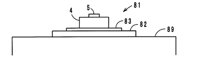
- the wireless IC device 81 is a patch type in which a radiation plate 83 is formed of a metal foil or the like on a support 82 made of a flexible film having a relatively small area.
- the radiation plate 83 has an opening 87 and a slit portion 86 connected to the opening 87.
- the wireless IC device 81 is used by attaching the support 82 on an article 89. If the support 82 has a certain thickness through which magnetic flux passes, the article may be a metal.
- the wireless IC device 91 includes mounting electrodes 12 a and 12 b connected to the back surface of the feeder circuit board 4 via the coil pattern 23 and interlayer connection conductors 26 a and 26 b.
- the mounting electrodes 12a and 12b are formed and connected to the mounting electrodes 15a and 15b of the radiation plate 3 via a conductive bonding agent 16 such as solder.
- the mounting electrodes 15a and 15b are formed by openings in which a resist material coated on the surface of the radiation plate 3 is partially peeled off, similarly to the mounting electrode 15 described in the first embodiment. Other configurations are the same as those in the first embodiment.
- the coil pattern 23 of the power supply circuit board 4 and the radiation plate 3 are electromagnetically coupled, but also both are directly connected (coupled). Therefore, the gain of the radiation plate 3 is increased.
- FIGS. 16 to 19 show Modifications 1 to 4 in which openings are provided in the radiation plate so that magnetic flux can pass even when a plurality of wireless IC devices are stacked.
- a radiation plate 100 which is Modification 1 shown in FIG. 16 includes a first electrode 101 having an opening 107 and a slit 106 on which the feeder circuit board 4 is mounted, and an annular first electrode 101 surrounding the first electrode 101. 2 electrodes 108 and formed of metal foil or the like. The first and second electrodes 101 and 108 are integrally formed on a single plane and are electrically connected to each other at the connection portion 102.
- the magnetic flux passes through the opening 109 surrounded by the annular second electrode 108.
- the opening 107 on which the feeder circuit board 4 is mounted is preferably in the center of the annular second electrode 108. With this configuration, the power feeding circuit board 4 can receive the magnetic flux evenly.
- a radiation plate 110 which is Modification 2 shown in FIG. 17, includes a first electrode 111 having an opening 117 and a slit 116 in which the feeder circuit board 4 is mounted, and an annular first electrode 111 surrounding the first electrode 111. It consists of two electrodes 118 and is formed of metal foil or the like. The first and second electrodes 111 and 118 are integrally formed on a single plane and are electrically connected to each other at the connection portions 112 and 113. As described above, since the first electrode 111 and the second electrode 118 are connected at two locations, an electric signal generated by a magnetic field is efficiently transmitted to the feeder circuit board 4. In the second modification, the magnetic flux passes through the opening 119 surrounded by the annular second electrode 118.
- a radiation plate 120 which is a third modification shown in FIG. 18 includes a first electrode 121 having an opening 127 and a slit 126 in which the feeder circuit board 4 is mounted, and an annular first electrode 121 surrounding the first electrode 121. 2 electrodes 128.
- the first and second electrodes 121 and 128 are integrally formed on a single plane and are electrically connected to each other at the connection portion 122.
- the magnetic flux passes through the opening 129 surrounded by the annular second electrode 128.
- the magnetic flux passes through the opening 139 surrounded by the annular second electrode 138.
- the opening and the slit of the second electrode 138 are provided larger than the opening 137 and the slit 136 of the first electrode 131, whereby the first electrode 131 and the second electrode 131 are formed. Even when a slight positional shift occurs when the electrode 138 is attached, the width of the opening 137 and the slit 136 having a predetermined size included in the first electrode 131 can be secured.
- the wireless IC device according to the present invention is not limited to the above-described embodiments, and various modifications can be made within the scope of the gist thereof.
- the present invention is useful for a wireless IC device, and is particularly excellent in that the gain of a transmission / reception signal can be controlled.
Landscapes
- Engineering & Computer Science (AREA)
- Microelectronics & Electronic Packaging (AREA)
- Physics & Mathematics (AREA)
- Computer Hardware Design (AREA)
- General Physics & Mathematics (AREA)
- Theoretical Computer Science (AREA)
- Computer Networks & Wireless Communication (AREA)
- Electromagnetism (AREA)
- Near-Field Transmission Systems (AREA)
- Details Of Aerials (AREA)
Abstract
Description
本発明は、無線ICと放射板とを含んで構成される無線ICデバイス、特に、RFID(Radio Frequency Identification)システムに用いられる無線ICデバイスに関する。 The present invention relates to a wireless IC device including a wireless IC and a radiation plate, and more particularly to a wireless IC device used in an RFID (Radio Frequency Identification) system.
近年、物品の管理システムとして、誘導磁界を発生するリーダライタと、物品に付され、所定の情報を記憶したICタグ(以下、無線ICデバイスと称する)とを電磁界を利用した非接触方式で通信し、所定の情報を伝達するRFIDシステムが開発されている。 2. Description of the Related Art In recent years, as an article management system, a reader / writer that generates an induced magnetic field and an IC tag (hereinafter referred to as a wireless IC device) that is attached to an article and stores predetermined information are contactless using an electromagnetic field. RFID systems that communicate and communicate predetermined information have been developed.
このRFIDシステムに用いられる無線ICデバイスは、所定の無線信号を処理する無線ICチップと、無線信号の送受信を行う放射板とを備えており、例えば、特許文献1に記載のものが知られている。
A wireless IC device used in the RFID system includes a wireless IC chip that processes a predetermined wireless signal and a radiation plate that transmits and receives the wireless signal. For example, a device described in
特許文献1に記載の無線ICデバイスは、無線ICチップと、該無線ICチップを搭載し、所定の共振周波数を有する共振回路を含む給電回路を備えた給電回路基板と、該給電回路基板の下面に貼着されており、給電回路から供給された送信信号を放射し、受信信号を受けて給電回路に供給する放射板とを備えている。給電回路基板の共振回路の共振周波数が送受信信号の周波数に実質的に相当するように設計されており、極めて安定した周波数特性を有するものである。
A wireless IC device described in
特許文献1に記載された無線ICデバイスにおいて、放射板にて送受される無線信号の周波数は、給電回路基板の給電回路にて実質的に決められているため、放射板の大きさや形状にほとんど依存しない、という極めて優れた特性を有している。しかしながら、例えばその段落0020に記載されているように、無線信号の利得の大きさは、放射板の大きさや形状に依存する。つまり、放射板の大きさや形状などが異なると、これに伴って利得も変動してしまうが、利得の制御手段は、特許文献1には十分に開示されていない。
In the wireless IC device described in
本発明は前述の実情に鑑みてなされたものであり、その目的は、送受信信号の利得を制御可能な無線ICデバイスを提供することにある。 The present invention has been made in view of the above circumstances, and an object thereof is to provide a wireless IC device capable of controlling the gain of a transmission / reception signal.
前記目的を達成するため、本発明の一形態である無線ICデバイスは、
所定の無線信号を処理する無線ICと、
前記無線ICに接続され、少なくとも一つのコイルパターンを含んだ給電回路を有する給電回路基板と、
前記給電回路基板から供給された送信信号を放射する、及び/又は、受信信号を受けてこれを前記給電回路基板に供給する放射板と、を備え、
前記放射板は、その一部に開口部と該開口部に連接したスリット部とを有しており、前記コイルパターンの巻回軸方向から平面視したとき、前記放射板の開口部と前記コイルパターンの内側領域とが少なくとも一部で重なっていること、
を特徴とする。
In order to achieve the above object, a wireless IC device according to one aspect of the present invention includes:
A wireless IC for processing a predetermined wireless signal;
A power supply circuit board having a power supply circuit connected to the wireless IC and including at least one coil pattern;
A radiation plate that radiates a transmission signal supplied from the power supply circuit board and / or receives a reception signal and supplies the received signal to the power supply circuit board;
The radiation plate has an opening and a slit connected to the opening in a part thereof, and when viewed in plan from the winding axis direction of the coil pattern, the opening of the radiation plate and the coil At least partly overlaps the inner area of the pattern,
It is characterized by.
本発明に係る無線ICデバイスによれば、特に、放射板はその一部に形成された開口部と該開口部に連接したスリット部とを有しており、給電回路基板に含まれたコイルパターンの巻回軸方向から平面視したときに、放射板の開口部とコイルパターンの内側領域とが少なくとも一部で重なっているので、コイルパターンに電流が流れると、励起された磁界が放射板の開口部を通して理想的に分布し、この誘導磁界によって放射板における開口部周辺に誘導電流が励起され、この誘導電流にはスリット部にて電位差が与えられる。従って、このスリット部の長さや幅で誘導電流の量や分布を制御することにより、放射板の全域にて生じる電界・磁界の量を制御することができ、これによって、送受信信号の利得を制御することができる。 According to the wireless IC device according to the present invention, in particular, the radiation plate has an opening formed in a part thereof and a slit connected to the opening, and the coil pattern included in the feeder circuit board. When viewed in plan from the winding axis direction of the coil plate, the opening of the radiation plate and the inner region of the coil pattern overlap at least partially, so when a current flows through the coil pattern, the excited magnetic field is Ideally distributed through the opening, an induced current is excited around the opening in the radiation plate by the induced magnetic field, and a potential difference is given to the induced current at the slit. Therefore, by controlling the amount and distribution of the induced current with the length and width of the slit portion, the amount of electric and magnetic fields generated in the entire area of the radiation plate can be controlled, thereby controlling the gain of the transmission / reception signal. can do.
以下、本発明に係る無線ICデバイスを具体的な実施例に基づいて説明する。なお、各図において、共通する部品、部分には同じ符号を付し、重複する説明は省略する。 Hereinafter, the wireless IC device according to the present invention will be described based on specific embodiments. In addition, in each figure, the same code | symbol is attached | subjected to a common component and part, and the overlapping description is abbreviate | omitted.
(実施例1、図1~図7参照)
まず、主に図1を参照して実施例1の無線ICデバイスの構造を説明する。図1(A)などに示すように、無線ICデバイス1においては、例えばプリント配線基板で構成される支持基板2上に、例えば金属箔のような金属膜で形成された放射板3が形成されており、さらに放射板3の上には給電回路基板4が搭載されている。給電回路基板4は少なくとも一つのコイルパターンを含んだ給電回路を有しており、所定の無線信号を処理する無線ICチップ5が実装されている。即ち、無線ICチップ5は、給電回路基板4の一方主面4aに実装されており、給電回路基板4は、その他方主面4bを搭載面として放射板3に搭載されている。無線ICチップ5は、クロック回路、ロジック回路、メモリ回路などを含み、必要な情報がメモリされている。
(See Example 1, FIGS. 1 to 7)
First, the structure of the wireless IC device according to the first embodiment will be described mainly with reference to FIG. As shown in FIG. 1A and the like, in the
図1(B)などに示すように、給電回路基板4の一方主面4aには、無線ICチップ5を給電回路基板4に実装・接続するための複数の接続用電極11が設けられている。これらの接続用電極11は、無線ICチップ5の裏面に形成された複数の接続用電極(図示省略)と、はんだなどの導電性接合剤8(図10参照)を介してそれぞれ電気的に接続されている。その結果、無線ICチップ5が給電回路基板4の一方主面4aに実装される。また、給電回路基板4の他方主面4bには、給電回路基板4を放射板3に搭載するための搭載用電極12が設けられている。
As shown in FIG. 1B and the like, a plurality of
図1(C)などに示すように、放射板3には、その一部に開口部7が設けられており、該開口部7にはスリット部6が連接している。スリット部6の一方端は開口部7に連接し、他方端は放射板3の側縁にて開放されている。即ち、スリット部6は開口部7と放射板3の側縁とを連通させるように設けられている。なお、スリット部6の形状は、本実施例1のように直線状であることが加工性の点で有利であるが、ミアンダ状や湾曲状に形成されていても構わない。
As shown in FIG. 1C and the like, the
さらに、放射板3には、その開口部7の周囲部分に給電回路基板4を搭載・接続するための複数の搭載用電極15が設けられている。これらの搭載用電極15は、給電回路基板4の他方主面4bに設けられた搭載用電極12とはんだなどの導電性接合剤16(図5参照)を介して接続される。搭載用電極15は、放射板3の表面にコーティングしたレジスト材などからなる保護層14を部分的に剥離した開口によって形成されている。つまり、保護層14の開口部分によって放射板3の一部が搭載用電極15として形成されている。
Furthermore, the
なお、本実施例1では、給電回路基板4の他方主面4bに設けられた搭載用電極12は、給電回路基板4の内部に設けられた給電回路に直接的には接続されていない。この搭載用電極12がはんだなどの導電性接合剤16を介して放射板3の一部として形成された搭載用電極15に接合されている。
In the first embodiment, the mounting
放射板3は、図2に示すように、平面的に形成された矩形状をなしており、一側縁部であって長辺方向のほぼ中央部に、無線ICチップ5を搭載した給電回路基板4が実装されている。本実施例1においては、例えば、携帯電話やパーソナルコンピュータなどの電子機器に内蔵され、所定の電子回路を構成するプリント配線基板に設けられたグランド電極を放射板3として利用することができる。即ち、放射板3は放射機能のみを持った素子として設けても構わないが、そのような素子でなくとも、様々な電子回路において用いられているグランド電極を放射板3として利用することもできる。
As shown in FIG. 2, the radiating
放射板3に設けられた開口部7は、給電回路基板4に設けられたコイルパターン23(図3参照)との関係では、該コイルパターン23の巻回軸方向から平面視したときにコイルパターン23の周回軌跡の内側領域の少なくとも一部で重なっている。図3に示すように、開口部7とコイルパターン23の内側領域とがほぼ全域で重なっており、かつ、開口部7の面積とコイルパターン23の内側領域の面積とがほぼ同一であることが好ましい。その理由は、コイルパターン23による磁界H(図5(A)参照)が放射板3に対して効率よく伝播し、損失が抑えられ、利得が向上するからである。
In relation to the coil pattern 23 (see FIG. 3) provided on the
ここで、本実施例1における給電回路基板4は、樹脂層やセラミック層などからなる複数の誘電体層が積層された積層体として構成されている。給電回路を構成するコイルパターン23は、複数の誘電体層にそれぞれ配置された複数の環状電極を積層方向にその巻回軸を有したヘリカル状に層間導体を介して接続したものである。但し、給電回路基板は単層基板上にコイルパターンが形成されたものであっても構わない。
Here, the power
即ち、図4に示すように、給電回路基板4には、ヘリカル状のコイルパターン23が内蔵されており、コイルパターン23を含む給電回路によって、無線ICチップ5からの送信信号を放射板3に供給し、放射板3からの受信信号(受信電力)を無線ICチップ5に供給する。
That is, as shown in FIG. 4, a
給電回路を具体的に説明すると、無線ICチップ5の接続用電極に接続される給電回路基板4側の接続用電極11aは、積層体中に設けられた層間接続導体21aを介して他の層に設けられたパッド導体22aに接続され、パッド導体22aはこの層においてコイルパターン23の一部を構成する配線導体23aによって環状となるように引き回され、同層に設けられたパッド導体24aに接続されている。パッド導体24aは、層間接続導体21bを介して他の層に設けられたパッド導体22bに接続され、パッド導体22bはこの層においてコイルパターン23の一部を構成する配線導体23bによって環状となるように引き回され、同層に設けられたパッド導体24bに接続されている。
The power supply circuit will be described in detail. The connection electrode 11a on the power
さらに、パッド導体24bは、層間接続導体21cを介して他の層に設けられたパッド導体22cに接続され、パッド導体22cはこの層においてコイルパターン23の一部を構成する配線導体23cによって環状となるように引き回され、同層に設けられたパッド導体24cに接続されている。さらに、パッド導体24cは、層間接続導体21dを介して他の層に設けられたパッド導体22dに接続され、パッド導体22dはこの層においてコイルパターン23の一部を構成する配線導体23dによって環状となるように引き回され、同層に設けられたパッド導体24dに接続されている。
Further, the
さらに、パッド導体24dは、層間接続導体21eを介して他の層に設けられたパッド導体22eに接続され、パッド導体22eはこの層においてコイルパターン23の一部を構成する配線導体23eによって環状となるように引き回され、同層に設けられたパッド導体24eに接続されている。さらに、パッド導体24eは、層間接続導体21fを介して他の層に設けられたパッド導体22fに接続され、パッド導体22fはこの層においてコイルパターン23の一部を構成する配線導体23fによって環状となるように引き回され、同層に設けられたパッド導体24fに接続されている。そして、パッド導体24fは、層間接続導体25を介して、無線ICチップ5の他の接続用電極に接続される給電回路基板4側の接続用電極11bに接続されている。
Further, the
即ち、層間接続導体21a~21f、パッド導体22a~22f、環状の配線導体23a~23f、パッド導体24a~24f及び層間接続導体25によってコイルパターン23が形成されている。なお、給電回路基板4を構成する積層体の表面には、電極11c,11dが設けられており、これらは無線ICチップ5を実装する際の固定用電極であって、給電回路基板4に設けられたコイルパターン23に接続されてはいない。
That is, the
前述のように、本実施例1において、放射板3はその一部に形成された開口部7とこの開口部7に連接したスリット部6とを有しており、給電回路基板4に形成されたコイルパターン23の巻回軸方向から平面視したときに、開口部7とコイルパターン23の内側領域とは重なっており、しかも、開口部7の面積とコイルパターン23の内側領域の面積とがほぼ同一である。従って、図5(A)に示すように、例えば、無線信号の送信時には、無線ICチップ5から信号電流がコイルパターン23に流され、この電流によって生じた誘導磁界Hは、開口部7を通して図中点線で示すように理想的に分布する。磁界Hが理想的に分布するとは、二つの磁界Hの中心Bが開口部7の中心と一致していることであり、この状態で放射板3の利得が最大となる。
As described above, in the first embodiment, the
前記誘導磁界Hによって、図5(B)に示すように、開口部7の周囲部分に、誘導電流I1,I2(但し、電流I1,I2の伝播方向は180°異なる)が生じる。ここで、開口部7にはスリット部6が連接されているため、この誘導電流I1,I2はスリット部6にてその流れが制限され、電位差が与えられる(容量が形成される)。従って、このスリット部6の長さL1や幅L2で、誘導電流I1,I2の量や分布を制御することにより、放射板3の全域に生じる電界・磁界の量を制御することができる。その結果、送信信号の利得を制御することができる。
The induced magnetic field H generates induced currents I1 and I2 (however, the propagation directions of the currents I1 and I2 differ by 180 °) in the peripheral portion of the
このように、放射板3においては、誘導電流I1,I2によって磁界Hが誘起され、図5(C)に示すように、この磁界Hによって電界Eが誘起され、この電界Eによって磁界Hが誘起されるという連鎖により、放射板3の全域に電磁界分布が二次元的に広がる。この電磁界分布によって、無線信号が送信される。従って、この無線ICデバイス1で取り扱われる無線信号は、高周波帯域、特にUHF帯の信号であることが好ましい。
Thus, in the
前述したように、スリット部6の長さL1や幅L2により、放射板3にて送受信される無線信号の利得を制御できる。具体的には、スリット部6の長さL1を大きくするほど、また、幅L2を小さくするほど、利得が大きくなる傾向にある。
As described above, the gain of the radio signal transmitted and received by the
図5(A)に示すように、給電回路基板4に形成した搭載用電極12は、コイルパターン23の巻回軸方向から平面視したとき、その主要部がコイルパターン23の内側領域以外の領域に形成されていることが好ましい。即ち、搭載用電極12は、理想的な磁界Hの形成の妨げとならないように、特に開口部7を通る磁界Hの妨げとならないように配置することが好ましく、さらに、コイルパターン23の投射面内に搭載用電極12の主要部が重なっていることが好ましい。同様の理由で、放射板3側の搭載用電極15も、コイルパターン23の巻回軸方向から平面視したとき、その主要部がコイルパターン23の内側領域以外の領域に形成されていることが好ましく、さらに、コイルパターン23の投射面内に搭載用電極15の主要部が重なっていることが好ましい。
As shown in FIG. 5A, the mounting
図4及び図5(A)に示したように、各誘電体層に設けられた環状導体(配線導体23b~23f)は、それぞれ所定間隔をおいて平行な複数の線路導体によって形成されていることが好ましい。即ち、本実施例1において、環状に形成されている配線導体23b~23fは両端部に配置されたパッド導体をつなぐ平行な2本の線路導体として形成されており、これによって、2本の線路導体の間にも磁束が通るようになり、励起された磁界がコイルパターン23の中心方向、即ち、巻回軸と直交する方向に広がって、磁束を効率的に利用できるようになる。また、環状導体の並列本数を増やすことで、環状導体の直流抵抗を小さくできる効果を生じる。この結果、無線信号の利得を向上させることができる。
As shown in FIGS. 4 and 5A, the annular conductors (wiring
図6に示すように本実施例1の無線ICデバイス1は、差動出力型の無線ICチップ5を備えており、二つの入出力電極間にコイルパターン23が直列的に接続された構造とされている。そして、コイルパターン23に誘起された誘導磁界Hが放射板3の開口部7を通して理想的なかたちで開口部7の周囲部分に伝達する。
As shown in FIG. 6, the
この等価回路図では、給電回路としてコイルパターン23のみを図示しているが、インダクタンス成分としてコイルパターン23自体のインダクタンスを利用しているほか、コイルパターン23は前述のように積層された環状電極によって形成されているので、各層の環状電極間に形成された浮遊容量をキャパシタンス成分として利用している。なお、給電回路基板4に設けられる給電回路は、少なくともコイルパターンを備えていればよく、給電回路が所定の共振周波数を持っている場合は、例えばその共振周波数を調整するためのキャパシタンス成分やインダクタンス成分をさらに有していても構わない。
In this equivalent circuit diagram, only the
本実施例1において、給電回路基板4の給電回路は所定の共振周波数を有しており、放射板3にて送受信される無線信号の周波数はこの共振周波数に実質的に相当するものであることが好ましい。ここで、「実質的に相当する」とは、給電回路が有する共振周波数の帯域と放射板3にて送受信される無線信号の周波数帯とがほぼ一致していることをいう。このように、送信信号及び/又は受信信号の周波数が給電回路の共振周波数に実質的に相当しているので、放射板3の大きさや形状、放射板3を支持する支持基板2の形状や材質などにほとんど依存しない安定した周波数特性を有する無線ICデバイスが得られる。
In the first embodiment, the power supply circuit of the power
本実施例1においては、図7に示すように、放射板3における開口部7の周辺部分の面積、つまりコイルパターン23によって誘起された磁束を受ける部分の面積は、コイルパターン23の巻回軸方向の長さ、即ちコイルパターン23の積層方向の厚みをT1とし、コイルパターン23の外延端に相当する位置10aから放射板3における開口部7の周縁端10bの長さをT2としたとき、T2>T1であることが好ましい。放射板3の開口部7周辺部分のサイズとコイルパターン23のサイズをこのような関係とすることにより、コイルパターン23による磁束を放射板3側で約80%以上の高効率で受けることができ、損失が少なく、利得の大きな無線ICデバイスを構成することができる。
In the first embodiment, as shown in FIG. 7, the area of the peripheral portion of the
なお、本実施例1において、給電回路基板4と放射板3とは主として磁界によって結合しているので、給電回路基板4と放射板3との間のインピーダンス整合を考慮する必要は必ずしもない。つまり、本実施例1によれば、前述したように、スリット部6の形状を好ましく設計することにより、極めて容易に無線信号の利得を制御することができる。
In the first embodiment, since the
(実施例2、図8参照)
図8(A)に示すように、本実施例2の無線ICデバイス31は、基本的には前記実施例1の無線ICデバイス1と同様に構成されており、給電回路基板34が放射板33の側縁部に配置されている点で、実施例1の無線ICデバイスとは異なっている。無線ICデバイス31においては、放射板33の側縁部から開口部37までのスリット部36の長さ(図5(B)のL1参照)が短くなり、利得は小さくなる傾向にある。なお、図8(B)に示すように、放射板33'に形成されるスリット部36'の幅が開口部37'の幅とほぼ同一であっても構わない。
(See Example 2, FIG. 8)
As shown in FIG. 8A, the
ここで、放射板33を長さ14cm、幅4cmとした場合、スリット部36の長さL1の数値に応じた利得の具体的数値について示す。
L1=0mmのとき、利得は-14.4dB
L1=0.5mmのとき、利得は-13.1dB
L1=1.0mmのとき、利得は-11.6dB
L1=1.5mmのとき、利得は-10.9dB
L1=2.5mmのとき、利得は-9.4dB
L1=4.5mmのとき、利得は-7.9dB
Here, when the
When L1 = 0mm, the gain is -14.4dB.
When L1 = 0.5mm, the gain is -13.1dB.
When L1 = 1.0mm, the gain is -11.6dB
When L1 = 1.5mm, the gain is -10.9dB
When L1 = 2.5mm, the gain is -9.4dB
When L1 = 4.5mm, the gain is -7.9dB
(コイルパターンの変形例、図9参照)
前記給電回路基板4の内部に設けられるコイルパターン23は、図9に示すように、各誘電体層に設けられる環状導体が1本の線路導体で形成されていても構わない。図4に示したコイルパターン23は5層に設けた配線導体23b~23fによって構成されているが、図9に示すコイルパターン23は4層に設けた配線導体23b~23eにて構成されている。
(Modification of coil pattern, see FIG. 9)
As shown in FIG. 9, in the
この変形例のように、各誘電体層に設けられる環状導体(配線導体23b~23e)が1本の線路導体で形成されている場合、図4に示した構造に比べて、コイルパターン23による誘導磁界の二次元的な分布量が小さくなり、利得が小さくなる傾向にあるが、構成がシンプルになり、給電回路基板4の小型化を達成できる。
When the annular conductors (wiring
(実施例3、図10参照)
本実施例3の無線ICデバイス61は、図10に示すように、主に放射板63が支持基板62の内部に設けられている点で、前記実施例1の無線ICデバイス1と異なっている。即ち、放射板63は支持基板(例えば、プリント配線基板)62の内層に設けたグランド電極を利用している。
(See Example 3, FIG. 10)
As shown in FIG. 10, the
具体的には、図10に示すように、無線ICデバイス61においては、プリント配線基板である支持基板62の内部に、図示しないスリット部を連接した開口部67を有する放射板63が形成されており、さらに支持基板62には給電回路基板4が搭載されている。給電回路基板4はコイルパターン23を含む給電回路を有しており、さらにその表面には所定の無線信号を処理する無線ICチップ5が実装されている。
Specifically, as shown in FIG. 10, in the
支持基板62の表面には、給電回路基板4を搭載・固定するための搭載用電極68が設けられており、給電回路基板4の他方主面4bに設けられた搭載用電極12とはんだなどの導電性接合剤16を介して接続されている。また、給電回路基板4側の搭載用電極12は、給電回路基板4の内部に設けられた給電回路には直接的に接続されていない。同様に、支持基板62側の搭載用電極68も支持基板62の内部に形成された放射板63に直接的に接続されていない。
A mounting
(実施例4、図11参照)
本実施例4の無線ICデバイス71は、図11に示すように、いわゆるタグ型(インレイ型)の無線ICデバイスである。即ち、この無線ICデバイス71は、PETフィルムのような可撓性の支持体72の上に、金属箔のような可撓性の金属膜によって形成された放射板73が設けられた構造を有している。放射板73は、スリット部76が連接された開口部77の周辺部、つまり給電回路基板のコイルパターンによって誘起された磁束を受ける平面状部分78と、主に無線信号の送受信を行うミアンダ状部分79とを有している。但し、磁束を受ける平面状部分78と無線信号の送受信を行うミアンダ状部分79との間に明確な境界があるわけではない。前記実施例1の無線ICデバイス1と同様に、開口部77の周囲には、給電回路基板を搭載するための搭載用電極75が、レジスト材を部分的に剥離することにより設けられている。この無線ICデバイス71は、各種の商品に固定され、商品の流通履歴管理などに用いることができる。
(See Example 4, FIG. 11)
As shown in FIG. 11, the
このように、本発明に係る無線ICデバイスにおいて、放射板を支持する支持体は、プリント配線基板のようなリジッドな基板だけでなく、本実施例4に示したように、PETフィルムのようなフレキシブルな支持体72であってもよい。同様に、放射板自体も、焼結金属や金属板のようなリジッドなものだけでなく、金属箔のようなフレキシブルなものであってもよい。また、金属製のメガネフレームや指輪などの金属の一部を放射板とすることもできる。
As described above, in the wireless IC device according to the present invention, the support for supporting the radiation plate is not only a rigid substrate such as a printed wiring board, but also a PET film such as that shown in the fourth embodiment. A
(実施例5、図12及び図13参照)
本実施例5の無線ICデバイス81は、図12に示すように、比較的小さい面積の可撓性フィルムなどからなる支持体82上に放射板83を金属箔などで形成したもので、パッチ型の形状をなしており、放射板83は開口部87とそれに連接するスリット部86を有している。
(See Example 5, FIGS. 12 and 13)
As shown in FIG. 12, the
図13に示すように、この無線ICデバイス81は、物品89上に前記支持体82を貼着して用いられる。支持体82に磁束が通過するある程度の厚みがあれば、物品は金属であってもよい。
As shown in FIG. 13, the
(実施例6、図14及び図15参照)
本実施例6の無線ICデバイス91は、図14及び図15に示すように、給電回路基板4の裏面にコイルパターン23と層間接続導体26a,26bを介して接続した搭載用電極12a,12bを形成し、この搭載用電極12a,12bを放射板3の搭載用電極15a,15bにはんだなどの導電性接合剤16を介して接続したものである。搭載用電極15a,15bは、実施例1に説明した搭載用電極15と同様に、放射板3の表面にコーティングしたレジスト材を部分的に剥離した開口によって形成されている。なお、他の構成は実施例1と同様である。
(See Example 6, FIGS. 14 and 15)
As shown in FIGS. 14 and 15, the wireless IC device 91 according to the sixth embodiment includes mounting
即ち、本実施例6は、給電回路基板4のコイルパターン23と放射板3とが電磁界的に結合しているのみならず、両者が直接的にも接続(結合)されている。それゆえ、放射板3の利得が大きくなる。
That is, in the sixth embodiment, not only the
(放射板の変形例1~4、図16~図19参照)
ところで、放射板を比較的広い面積で一様に形成した複数の無線ICデバイスを重ねると、放射板が磁束を遮断してしまう。このような状態が生じると、無線ICデバイスとリーダライタとの送受信ができなくなる。そこで、以下の図16~19に、複数の無線ICデバイスが重ねられた場合でも、磁束が通過できるように放射板に開口を設けた変形例1~4を示す。変形例1~4に示すような開口(磁束の通過部分)を放射板に設けることにより、複数の無線ICデバイスを重ねた場合でも、磁束が開口を通過することによってリーダライタとの送受信が可能になる。また、環状の電極を有することで、放射板にとっては磁束を受ける面積が増加することになり、アンテナとしての利得が大きくなる。
(Refer to
By the way, if a plurality of wireless IC devices in which the radiation plate is uniformly formed in a relatively wide area are stacked, the radiation plate blocks the magnetic flux. When such a state occurs, transmission / reception between the wireless IC device and the reader / writer becomes impossible. Therefore, FIGS. 16 to 19 below
図16に示す変形例1である放射板100は、前記給電回路基板4が搭載される開口部107とスリット部106を有する第1の電極101と、該第1の電極101を囲む環状の第2の電極108とからなり、金属箔などで形成されている。第1及び第2の電極101,108は一平面上に一体的に形成され、接続部102にて互いに電気的に接続されている。本変形例1では、環状の第2の電極108で囲まれている開口109を磁束が通過することになる。なお、給電回路基板4が搭載される開口部107は環状の第2の電極108の中央部にあることが好ましい。この構成により、給電回路基板4が磁束を均等に受けることができる。
A
図17に示す変形例2である放射板110は、前記給電回路基板4が搭載される開口部117とスリット部116を有する第1の電極111と、該第1の電極111を囲む環状の第2の電極118とからなり、金属箔などで形成されている。第1及び第2の電極111,118は一平面上に一体的に形成され、接続部112,113にて互いに電気的に接続されている。このように、2箇所で第1の電極111と第2の電極118が接続されているので、磁界による電気信号が給電回路基板4に効率的に伝達される。本変形例2では、環状の第2の電極118で囲まれている開口119を磁束が通過することになる。
A
図18に示す変形例3である放射板120は、前記給電回路基板4が搭載される開口部127とスリット部126を有する第1の電極121と、該第1の電極121を囲む環状の第2の電極128とで構成されている。第1及び第2の電極121,128は一平面上に一体的に形成され、接続部122にて互いに電気的に接続されている。本変形例3では、環状の第2の電極128で囲まれている開口129を磁束が通過することになる。
A
図19に示す変形例4である放射板130は、第1の電極131と第2の電極138とを別体に形成し、第1の電極131を第2の電極138上に貼着したものである。貼着には非導電性接着剤又は導電性接着剤のいずれを用いてもよい。また、第1の電極131と第2の電極138同士が対向するように貼着してもよいし、表面に第1の電極131を形成したフィルムと第2の電極138が対向するように貼着してもよい。電極131が電極138に貼着されていても磁界は伝搬される。第1の電極131には前記給電回路基板4が搭載される開口部137とスリット136を有している。第2の電極138は前記変形例2と同じ形状を有している。本変形例4においても、環状の第2の電極138で囲まれている開口139を磁束が通過することになる。なお、変形例4において、第2の電極138の開口部及びスリット部を、第1の電極131の開口部137及びスリット136よりも大きく設けておくことにより、第1の電極131と第2の電極138とを貼着する際に、多少の位置ずれが生じても、第1の電極131が有する所定の大きさの開口部137及びスリット136幅を確保することができる。
A
(他の実施例)
なお、本発明に係る無線ICデバイスは前記実施例に限定するものではなく、その要旨の範囲内で種々に変更できることは勿論である。
(Other examples)
Of course, the wireless IC device according to the present invention is not limited to the above-described embodiments, and various modifications can be made within the scope of the gist thereof.
以上のように、本発明は、無線ICデバイスに有用であり、特に、送受信信号の利得を制御可能である点で優れている。 As described above, the present invention is useful for a wireless IC device, and is particularly excellent in that the gain of a transmission / reception signal can be controlled.
1,31,61,71,81,91…無線ICデバイス
2,62…支持基板
3,33,63,73,83,100,110,120,130…放射板
4,34…給電回路基板
5…無線ICチップ
6,36,76,86,106,116,126,136…スリット部
7,37,67,77,87,107,117,127,137…開口部
72,82…支持体
101,111,121,131…第1の電極
108,118,128,138…第2の電極
DESCRIPTION OF
Claims (13)
前記無線ICに接続され、少なくとも一つのコイルパターンを含んだ給電回路を有する給電回路基板と、
前記給電回路基板から供給された送信信号を放射する、及び/又は、受信信号を受けてこれを前記給電回路基板に供給する放射板と、を備え、
前記放射板は、その一部に開口部と該開口部に連接したスリット部とを有しており、前記コイルパターンの巻回軸方向から平面視したとき、前記放射板の開口部と前記コイルパターンの内側領域とが少なくとも一部で重なっていること、
を特徴とする無線ICデバイス。 A wireless IC for processing a predetermined wireless signal;
A power supply circuit board having a power supply circuit connected to the wireless IC and including at least one coil pattern;
A radiation plate that radiates a transmission signal supplied from the power supply circuit board and / or receives a reception signal and supplies the received signal to the power supply circuit board;
The radiation plate has an opening and a slit connected to the opening in a part thereof, and when viewed in plan from the winding axis direction of the coil pattern, the opening of the radiation plate and the coil At least partly overlaps the inner area of the pattern,
A wireless IC device characterized by the above.
Priority Applications (10)
| Application Number | Priority Date | Filing Date | Title |
|---|---|---|---|
| JP2010506742A JP4609604B2 (en) | 2008-05-21 | 2009-05-08 | Wireless IC device |
| CN200980118462.0A CN102037605B (en) | 2008-05-21 | 2009-05-08 | Wireless IC device |
| EP09750476.5A EP2284949B1 (en) | 2008-05-21 | 2009-05-08 | Wireless ic device |
| US12/903,242 US8960557B2 (en) | 2008-05-21 | 2010-10-13 | Wireless IC device |
| US13/585,866 US8590797B2 (en) | 2008-05-21 | 2012-08-15 | Wireless IC device |
| US14/054,865 US9022295B2 (en) | 2008-05-21 | 2013-10-16 | Wireless IC device |
| US14/162,806 US8973841B2 (en) | 2008-05-21 | 2014-01-24 | Wireless IC device |
| US14/596,458 US9489605B2 (en) | 2008-05-21 | 2015-01-14 | Wireless IC device |
| US15/285,541 US9652706B2 (en) | 2008-05-21 | 2016-10-05 | Wireless IC device |
| US15/479,524 US10534992B2 (en) | 2008-05-21 | 2017-04-05 | Wireless IC device |
Applications Claiming Priority (4)
| Application Number | Priority Date | Filing Date | Title |
|---|---|---|---|
| JP2008133335 | 2008-05-21 | ||
| JP2008-133335 | 2008-05-21 | ||
| JP2008239826 | 2008-09-18 | ||
| JP2008-239826 | 2008-09-18 |
Related Child Applications (2)
| Application Number | Title | Priority Date | Filing Date |
|---|---|---|---|
| EP14178344.9A Previously-Filed-Application EP2840648B1 (en) | 2008-05-21 | 2009-05-08 | Wireless IC device |
| US12/903,242 Continuation US8960557B2 (en) | 2008-05-21 | 2010-10-13 | Wireless IC device |
Publications (1)
| Publication Number | Publication Date |
|---|---|
| WO2009142114A1 true WO2009142114A1 (en) | 2009-11-26 |
Family
ID=41340046
Family Applications (1)
| Application Number | Title | Priority Date | Filing Date |
|---|---|---|---|
| PCT/JP2009/058682 Ceased WO2009142114A1 (en) | 2008-05-21 | 2009-05-08 | Wireless ic device |
Country Status (5)
| Country | Link |
|---|---|
| US (7) | US8960557B2 (en) |
| EP (3) | EP2284949B1 (en) |
| JP (1) | JP4609604B2 (en) |
| CN (3) | CN103729676B (en) |
| WO (1) | WO2009142114A1 (en) |
Cited By (59)
| Publication number | Priority date | Publication date | Assignee | Title |
|---|---|---|---|---|
| JP2011249937A (en) * | 2010-05-24 | 2011-12-08 | Tdk Corp | Proximity antenna and radio communication device |
| JP2011249938A (en) * | 2010-05-24 | 2011-12-08 | Tdk Corp | Proximity antenna and radio communication device |
| JP2011249935A (en) * | 2010-05-24 | 2011-12-08 | Tdk Corp | Proximity antenna and radio communication device |
| WO2011158844A1 (en) * | 2010-06-18 | 2011-12-22 | 株式会社村田製作所 | Communication terminal apparatus and antenna device |
| WO2012014939A1 (en) * | 2010-07-28 | 2012-02-02 | 株式会社村田製作所 | Antenna device and communications terminal device |
| EP2372840A3 (en) * | 2010-03-17 | 2012-07-04 | Panasonic Corporation | Antenna portable terminal using the same |
| CN102880898A (en) * | 2011-07-13 | 2013-01-16 | 上海铁勋智能识别系统有限公司 | Ultrahigh frequency (UHF) electronic tag capable of covering UHF full frequency range and sharing with free space and metal surface |
| WO2013115148A1 (en) * | 2012-02-01 | 2013-08-08 | 株式会社村田製作所 | Antenna apparatus and communication terminal apparatus |
| WO2013115147A1 (en) * | 2012-02-01 | 2013-08-08 | 株式会社村田製作所 | Antenna apparatus and communication terminal apparatus |
| US8613395B2 (en) | 2011-02-28 | 2013-12-24 | Murata Manufacturing Co., Ltd. | Wireless communication device |
| US8662403B2 (en) | 2007-07-04 | 2014-03-04 | Murata Manufacturing Co., Ltd. | Wireless IC device and component for wireless IC device |
| US8690070B2 (en) | 2009-04-14 | 2014-04-08 | Murata Manufacturing Co., Ltd. | Wireless IC device component and wireless IC device |
| US8704716B2 (en) | 2009-11-20 | 2014-04-22 | Murata Manufacturing Co., Ltd. | Antenna device and mobile communication terminal |
| US8720789B2 (en) | 2012-01-30 | 2014-05-13 | Murata Manufacturing Co., Ltd. | Wireless IC device |
| US8740093B2 (en) | 2011-04-13 | 2014-06-03 | Murata Manufacturing Co., Ltd. | Radio IC device and radio communication terminal |
| KR101414779B1 (en) * | 2010-10-20 | 2014-07-03 | 한국전자통신연구원 | Wireless power transfer device |
| US8770489B2 (en) | 2011-07-15 | 2014-07-08 | Murata Manufacturing Co., Ltd. | Radio communication device |
| US8797225B2 (en) | 2011-03-08 | 2014-08-05 | Murata Manufacturing Co., Ltd. | Antenna device and communication terminal apparatus |
| US8797148B2 (en) | 2008-03-03 | 2014-08-05 | Murata Manufacturing Co., Ltd. | Radio frequency IC device and radio communication system |
| WO2014123052A1 (en) * | 2013-02-06 | 2014-08-14 | 株式会社村田製作所 | Coil device and antenna device |
| US8814056B2 (en) | 2011-07-19 | 2014-08-26 | Murata Manufacturing Co., Ltd. | Antenna device, RFID tag, and communication terminal apparatus |
| US8853549B2 (en) | 2009-09-30 | 2014-10-07 | Murata Manufacturing Co., Ltd. | Circuit substrate and method of manufacturing same |
| US8878739B2 (en) | 2011-07-14 | 2014-11-04 | Murata Manufacturing Co., Ltd. | Wireless communication device |
| US8905296B2 (en) | 2011-12-01 | 2014-12-09 | Murata Manufacturing Co., Ltd. | Wireless integrated circuit device and method of manufacturing the same |
| US8917211B2 (en) | 2008-11-17 | 2014-12-23 | Murata Manufacturing Co., Ltd. | Antenna and wireless IC device |
| US8937576B2 (en) | 2011-04-05 | 2015-01-20 | Murata Manufacturing Co., Ltd. | Wireless communication device |
| US8941552B2 (en) | 2010-02-19 | 2015-01-27 | Murata Manufacturing Co., Ltd. | Composite printed wiring board and wireless communication system |
| US8944335B2 (en) | 2010-09-30 | 2015-02-03 | Murata Manufacturing Co., Ltd. | Wireless IC device |
| US8976075B2 (en) | 2009-04-21 | 2015-03-10 | Murata Manufacturing Co., Ltd. | Antenna device and method of setting resonant frequency of antenna device |
| US8973841B2 (en) | 2008-05-21 | 2015-03-10 | Murata Manufacturing Co., Ltd. | Wireless IC device |
| US8991713B2 (en) | 2011-01-14 | 2015-03-31 | Murata Manufacturing Co., Ltd. | RFID chip package and RFID tag |
| US9024837B2 (en) | 2010-03-31 | 2015-05-05 | Murata Manufacturing Co., Ltd. | Antenna and wireless communication device |
| US9024725B2 (en) | 2009-11-04 | 2015-05-05 | Murata Manufacturing Co., Ltd. | Communication terminal and information processing system |
| US9104950B2 (en) | 2009-01-30 | 2015-08-11 | Murata Manufacturing Co., Ltd. | Antenna and wireless IC device |
| US9117157B2 (en) | 2009-10-02 | 2015-08-25 | Murata Manufacturing Co., Ltd. | Wireless IC device and electromagnetic coupling module |
| US9166291B2 (en) | 2010-10-12 | 2015-10-20 | Murata Manufacturing Co., Ltd. | Antenna device and communication terminal apparatus |
| US9165239B2 (en) | 2006-04-26 | 2015-10-20 | Murata Manufacturing Co., Ltd. | Electromagnetic-coupling-module-attached article |
| US9236651B2 (en) | 2010-10-21 | 2016-01-12 | Murata Manufacturing Co., Ltd. | Communication terminal device |
| US9281873B2 (en) | 2008-05-26 | 2016-03-08 | Murata Manufacturing Co., Ltd. | Wireless IC device system and method of determining authenticity of wireless IC device |
| US9378452B2 (en) | 2011-05-16 | 2016-06-28 | Murata Manufacturing Co., Ltd. | Radio IC device |
| WO2016132654A1 (en) * | 2015-02-16 | 2016-08-25 | 株式会社村田製作所 | Antenna device and communication terminal apparatus |
| JP2016167274A (en) * | 2014-11-07 | 2016-09-15 | 株式会社村田製作所 | Wireless communication device and manufacturing method thereof |
| US9543642B2 (en) | 2011-09-09 | 2017-01-10 | Murata Manufacturing Co., Ltd. | Antenna device and wireless device |
| WO2017022554A1 (en) * | 2015-08-03 | 2017-02-09 | 株式会社村田製作所 | Antenna apparatus and electronic device |
| US9692128B2 (en) | 2012-02-24 | 2017-06-27 | Murata Manufacturing Co., Ltd. | Antenna device and wireless communication device |
| KR101760233B1 (en) | 2017-03-31 | 2017-07-20 | 삼성전자주식회사 | Electronic device comprising coil |
| US9727765B2 (en) | 2010-03-24 | 2017-08-08 | Murata Manufacturing Co., Ltd. | RFID system including a reader/writer and RFID tag |
| US9761923B2 (en) | 2011-01-05 | 2017-09-12 | Murata Manufacturing Co., Ltd. | Wireless communication device |
| US9830552B2 (en) | 2007-07-18 | 2017-11-28 | Murata Manufacturing Co., Ltd. | Radio IC device |
| WO2018079718A1 (en) * | 2016-10-29 | 2018-05-03 | 株式会社フェニックスソリューション | Antenna-mounted communication ic unit and antenna-mounted communication ic unit equipped with conductor |
| US10013650B2 (en) | 2010-03-03 | 2018-07-03 | Murata Manufacturing Co., Ltd. | Wireless communication module and wireless communication device |
| WO2018123432A1 (en) * | 2016-12-30 | 2018-07-05 | 株式会社フェニックスソリューション | Booster antenna, communication ic unit equipped with booster antenna, and communication ic unit equipped with booster antenna having attached conductor |
| US10235544B2 (en) | 2012-04-13 | 2019-03-19 | Murata Manufacturing Co., Ltd. | Inspection method and inspection device for RFID tag |
| US10592893B2 (en) | 2016-02-04 | 2020-03-17 | Samsung Electronics Co. Ltd | Electronic device including coil |
| WO2020110930A1 (en) | 2018-11-29 | 2020-06-04 | 京セラ株式会社 | Rfid tag |
| KR102213052B1 (en) * | 2019-11-13 | 2021-02-08 | 한국과학기술원 | Pcb coil for wireless power transter |
| JPWO2021229857A1 (en) * | 2020-05-15 | 2021-11-18 | ||
| US11354558B2 (en) | 2013-01-18 | 2022-06-07 | Amatech Group Limited | Contactless smartcards with coupling frames |
| JP2023509910A (en) * | 2019-12-28 | 2023-03-10 | エイヴェリー デニソン リテール インフォメーション サービシズ リミテッド ライアビリティ カンパニー | RFID device with multi-layer reactive straps and related systems and methods |
Families Citing this family (56)
| Publication number | Priority date | Publication date | Assignee | Title |
|---|---|---|---|---|
| US7519328B2 (en) | 2006-01-19 | 2009-04-14 | Murata Manufacturing Co., Ltd. | Wireless IC device and component for wireless IC device |
| JP4281850B2 (en) | 2006-06-30 | 2009-06-17 | 株式会社村田製作所 | optical disk |
| DE112007002024B4 (en) | 2006-09-26 | 2010-06-10 | Murata Mfg. Co., Ltd., Nagaokakyo-shi | Inductively coupled module and element with inductively coupled module |
| CN102982366B (en) | 2007-04-26 | 2016-04-13 | 株式会社村田制作所 | Wireless IC device |
| EP2148449B1 (en) | 2007-05-11 | 2012-12-12 | Murata Manufacturing Co., Ltd. | Wireless ic device |
| CN101542831B (en) | 2007-07-09 | 2014-06-25 | 株式会社村田制作所 | Wireless ic device |
| KR101037035B1 (en) | 2007-07-17 | 2011-05-25 | 가부시키가이샤 무라타 세이사쿠쇼 | Wireless IC Devices and Electronics |
| WO2009011376A1 (en) * | 2007-07-18 | 2009-01-22 | Murata Manufacturing Co., Ltd. | Wireless ic device |
| WO2010021217A1 (en) | 2008-08-19 | 2010-02-25 | 株式会社村田製作所 | Wireless ic device and method for manufacturing same |
| CN102273012B (en) | 2009-01-09 | 2013-11-20 | 株式会社村田制作所 | Wireless IC device and wireless IC module |
| JP5447515B2 (en) | 2009-06-03 | 2014-03-19 | 株式会社村田製作所 | Wireless IC device and manufacturing method thereof |
| JP5516580B2 (en) | 2009-06-19 | 2014-06-11 | 株式会社村田製作所 | Wireless IC device and method for coupling power feeding circuit and radiation plate |
| CN102474009B (en) | 2009-07-03 | 2015-01-07 | 株式会社村田制作所 | Antenna and antenna module |
| WO2011037234A1 (en) | 2009-09-28 | 2011-03-31 | 株式会社村田製作所 | Wireless ic device and method for detecting environmental conditions using same |
| WO2011045970A1 (en) | 2009-10-16 | 2011-04-21 | 株式会社村田製作所 | Antenna and wireless ic device |
| JP5418600B2 (en) | 2009-10-27 | 2014-02-19 | 株式会社村田製作所 | Transceiver and RFID tag reader |
| JP5299518B2 (en) | 2009-11-04 | 2013-09-25 | 株式会社村田製作所 | Information processing system |
| GB2487315B (en) | 2009-11-04 | 2014-09-24 | Murata Manufacturing Co | Communication terminal and information processing system |
| JP4978756B2 (en) | 2009-12-24 | 2012-07-18 | 株式会社村田製作所 | Communication terminal |
| JP5403146B2 (en) | 2010-03-03 | 2014-01-29 | 株式会社村田製作所 | Wireless communication device and wireless communication terminal |
| JP5477459B2 (en) | 2010-03-12 | 2014-04-23 | 株式会社村田製作所 | Wireless communication device and metal article |
| WO2012005278A1 (en) | 2010-07-08 | 2012-01-12 | 株式会社村田製作所 | Antenna and rfid device |
| WO2012020748A1 (en) | 2010-08-10 | 2012-02-16 | 株式会社村田製作所 | Printed wire board and wireless communication system |
| CN104701627B (en) | 2010-09-07 | 2018-11-20 | 株式会社村田制作所 | Antenna assembly |
| JP5609922B2 (en) * | 2011-08-10 | 2014-10-22 | 株式会社村田製作所 | Antenna device and communication terminal device |
| KR20130032545A (en) * | 2011-09-23 | 2013-04-02 | 삼성전자주식회사 | Mobile terminal having an antenna |
| WO2013069465A1 (en) | 2011-11-09 | 2013-05-16 | 株式会社村田製作所 | Antenna device and electronic device |
| KR101859575B1 (en) * | 2012-03-21 | 2018-05-18 | 삼성전자 주식회사 | Antenna device for near field wireless communication and electric device having the same |
| JP5772868B2 (en) * | 2012-05-21 | 2015-09-02 | 株式会社村田製作所 | ANTENNA DEVICE AND WIRELESS COMMUNICATION DEVICE |
| GB2539334A (en) * | 2012-10-26 | 2016-12-14 | Murata Manufacturing Co | Interface, communication apparatus, and program |
| JP5682739B2 (en) * | 2012-11-28 | 2015-03-11 | 株式会社村田製作所 | Interface and communication device |
| US20150009077A1 (en) * | 2013-07-03 | 2015-01-08 | Samsung Electronics Co., Ltd. | Cover of a mobile device and mobile device including the same |
| GB2516305A (en) * | 2013-07-19 | 2015-01-21 | Nokia Corp | Apparatus and methods for wireless communication |
| USD747298S1 (en) * | 2014-01-22 | 2016-01-12 | Agc Automotive Americas R&D, Inc. | Antenna |
| US9406996B2 (en) | 2014-01-22 | 2016-08-02 | Agc Automotive Americas R&D, Inc. | Window assembly with transparent layer and an antenna element |
| USD771602S1 (en) | 2014-01-22 | 2016-11-15 | Agc Automotive Americas R&D, Inc. | Antenna |
| USD774024S1 (en) | 2014-01-22 | 2016-12-13 | Agc Automotive Americas R&D, Inc. | Antenna |
| US9806398B2 (en) | 2014-01-22 | 2017-10-31 | Agc Automotive Americas R&D, Inc. | Window assembly with transparent layer and an antenna element |
| KR101762778B1 (en) | 2014-03-04 | 2017-07-28 | 엘지이노텍 주식회사 | Wireless communication and charge substrate and wireless communication and charge device |
| CN104051839B (en) * | 2014-06-27 | 2016-06-01 | 南通富士通微电子股份有限公司 | The forming method of RFID antenna |
| USD773442S1 (en) * | 2014-09-26 | 2016-12-06 | Megabyte Limited | RFID tag inlay |
| US10003218B2 (en) * | 2014-12-20 | 2018-06-19 | Intel Corporation | Chassis design for wireless-charging coil integration for computing systems |
| CN107454989B (en) * | 2015-01-27 | 2020-10-27 | 奥特斯奥地利科技与系统技术有限公司 | Electronic component and method for producing an electronic component |
| JP2016201082A (en) * | 2015-04-10 | 2016-12-01 | アイ・スマートソリューションズ株式会社 | Wireless tag unit |
| CN106207383A (en) * | 2015-05-06 | 2016-12-07 | 佳邦科技股份有限公司 | Communication module |
| KR102400978B1 (en) * | 2015-09-30 | 2022-05-23 | 삼성전자주식회사 | Circuit board in power supply, electronic apparatus including the same and inductor |
| EP3166181A1 (en) * | 2015-11-05 | 2017-05-10 | Gemalto Sa | Method for manufacturing a radiofrequency antenna on a mounting and antenna thus obtained |
| TWI580109B (en) * | 2015-12-01 | 2017-04-21 | 廣達電腦股份有限公司 | Mobile device |
| US10097030B2 (en) * | 2016-04-29 | 2018-10-09 | Taiwan Semiconductor Manufacturing Co., Ltd | Packaged semiconductor devices with wireless charging means |
| US10325707B2 (en) * | 2017-04-28 | 2019-06-18 | Teledyne Scientific & Imaging, Llc | Integrated field coil for compact atomic devices |
| US10790244B2 (en) | 2017-09-29 | 2020-09-29 | Taiwan Semiconductor Manufacturing Company, Ltd. | Semiconductor device and method |
| CN110011686B (en) * | 2018-01-03 | 2022-02-22 | 富顶精密组件(深圳)有限公司 | Wireless communication interconnection system and wall-mounted kit thereof |
| JP1647393S (en) * | 2018-02-01 | 2019-12-09 | ||
| KR102194290B1 (en) * | 2018-07-23 | 2020-12-22 | 동우 화인켐 주식회사 | Antenna structure and display device including the same |
| CN108958082A (en) * | 2018-09-04 | 2018-12-07 | 英曼医疗电子仪器(苏州)有限公司 | It tatoos sewing power supply wireless signal controller |
| JP7528956B2 (en) * | 2019-12-03 | 2024-08-06 | 戸田工業株式会社 | Antenna for module board and module board using same |
Citations (4)
| Publication number | Priority date | Publication date | Assignee | Title |
|---|---|---|---|---|
| JP2007096768A (en) * | 2005-09-29 | 2007-04-12 | Omron Corp | Antenna unit and non-contact IC tag |
| JP2007162805A (en) * | 2005-12-13 | 2007-06-28 | Mitsubishi Materials Corp | Tagged bolt |
| WO2007138857A1 (en) * | 2006-06-01 | 2007-12-06 | Murata Manufacturing Co., Ltd. | Radio frequency ic device and composite component for radio frequency ic device |
| JP2008097473A (en) * | 2006-10-16 | 2008-04-24 | Dainippon Printing Co Ltd | IC tag label |
Family Cites Families (576)
| Publication number | Priority date | Publication date | Assignee | Title |
|---|---|---|---|---|
| US3364564A (en) | 1965-06-28 | 1968-01-23 | Gregory Ind Inc | Method of producing welding studs dischargeable in end-to-end relationship |
| JPS5754964B2 (en) | 1974-05-08 | 1982-11-20 | ||
| JPS6193701A (en) | 1984-10-13 | 1986-05-12 | Toyota Motor Corp | Antenna system for automobile |
| JPS61284102A (en) | 1985-06-11 | 1986-12-15 | Oki Electric Ind Co Ltd | Antenna for portable radio equipment |
| JPS62127140U (en) | 1986-02-03 | 1987-08-12 | ||
| NL8700369A (en) * | 1987-02-16 | 1988-09-16 | Nedap Nv | METHOD FOR PLACING AN ELECTRONIC RESPONDER IN A METAL ENVIRONMENT |
| JPH01212035A (en) | 1987-08-13 | 1989-08-25 | Secom Co Ltd | Electromagnetic field diversity reception method |
| ZA89872B (en) | 1988-02-04 | 1990-10-31 | Uniscan Ltd | Concentrator |
| JPH0744114B2 (en) | 1988-12-16 | 1995-05-15 | 株式会社村田製作所 | Multilayer chip coil |
| JPH02164105A (en) | 1988-12-19 | 1990-06-25 | Mitsubishi Electric Corp | spiral antenna |
| US5253969A (en) | 1989-03-10 | 1993-10-19 | Sms Schloemann-Siemag Aktiengesellschaft | Feeding system for strip material, particularly in treatment plants for metal strips |
| JPH03171385A (en) | 1989-11-30 | 1991-07-24 | Sony Corp | Information card |
| JP2662742B2 (en) | 1990-03-13 | 1997-10-15 | 株式会社村田製作所 | Bandpass filter |
| JP2763664B2 (en) | 1990-07-25 | 1998-06-11 | 日本碍子株式会社 | Wiring board for distributed constant circuit |
| JPH04150011A (en) | 1990-10-12 | 1992-05-22 | Tdk Corp | Composite electronic component |
| JPH04167500A (en) | 1990-10-30 | 1992-06-15 | Omron Corp | Printed-circuit board management system |
| JP2539367Y2 (en) | 1991-01-30 | 1997-06-25 | 株式会社村田製作所 | Multilayer electronic components |
| NL9100176A (en) | 1991-02-01 | 1992-03-02 | Nedap Nv | Antenna configuration for contactless identification label - forms part of tuned circuit of ID or credit card interrogated via inductive coupling |
| JP2558330Y2 (en) | 1991-02-06 | 1997-12-24 | オムロン株式会社 | Electromagnetic coupling type electronic equipment |
| NL9100347A (en) | 1991-02-26 | 1992-03-02 | Nedap Nv | Integrated transformer circuit for ID or credit card - is interrogated via contactless inductive coupling using capacitor to form tuned circuit |
| JPH04321190A (en) | 1991-04-22 | 1992-11-11 | Mitsubishi Electric Corp | Antenna circuit and its production for non-contact type portable storage |
| JPH0745933Y2 (en) | 1991-06-07 | 1995-10-18 | 太陽誘電株式会社 | Multilayer ceramic inductance element |
| EP0522806B1 (en) | 1991-07-08 | 1996-11-20 | Nippon Telegraph And Telephone Corporation | Retractable antenna system |
| JP2839782B2 (en) | 1992-02-14 | 1998-12-16 | 三菱電機株式会社 | Printed slot antenna |
| JPH05327331A (en) | 1992-05-15 | 1993-12-10 | Matsushita Electric Works Ltd | Printed antenna |
| JP3186235B2 (en) | 1992-07-30 | 2001-07-11 | 株式会社村田製作所 | Resonator antenna |
| JPH0677729A (en) | 1992-08-25 | 1994-03-18 | Mitsubishi Electric Corp | Antenna integrated microwave circuit |
| JP2592328Y2 (en) | 1992-09-09 | 1999-03-17 | 神鋼電機株式会社 | Antenna device |
| JPH06177635A (en) | 1992-12-07 | 1994-06-24 | Mitsubishi Electric Corp | Cross dipole antenna system |
| JPH06260949A (en) | 1993-03-03 | 1994-09-16 | Seiko Instr Inc | Radio equipment |
| JPH07183836A (en) | 1993-12-22 | 1995-07-21 | San'eisha Mfg Co Ltd | Coupling filter device for distribution line carrier communication |
| US5491483A (en) | 1994-01-05 | 1996-02-13 | Texas Instruments Incorporated | Single loop transponder system and method |
| JP3427527B2 (en) | 1994-12-26 | 2003-07-22 | 凸版印刷株式会社 | Biodegradable laminate and biodegradable card |
| US6096431A (en) | 1994-07-25 | 2000-08-01 | Toppan Printing Co., Ltd. | Biodegradable cards |
| JP2999374B2 (en) | 1994-08-10 | 2000-01-17 | 太陽誘電株式会社 | Multilayer chip inductor |
| JP3141692B2 (en) | 1994-08-11 | 2001-03-05 | 松下電器産業株式会社 | Millimeter wave detector |
| DE4431754C1 (en) | 1994-09-06 | 1995-11-23 | Siemens Ag | Carrier element for ic module of chip card |
| US5528222A (en) | 1994-09-09 | 1996-06-18 | International Business Machines Corporation | Radio frequency circuit and memory in thin flexible package |
| JPH0887580A (en) | 1994-09-14 | 1996-04-02 | Omron Corp | Data carriers and ball games |
| JP3064840B2 (en) | 1994-12-22 | 2000-07-12 | ソニー株式会社 | IC card |
| JP2837829B2 (en) | 1995-03-31 | 1998-12-16 | 松下電器産業株式会社 | Inspection method for semiconductor device |
| JPH08279027A (en) | 1995-04-04 | 1996-10-22 | Toshiba Corp | Wireless communication card |
| US5955723A (en) | 1995-05-03 | 1999-09-21 | Siemens Aktiengesellschaft | Contactless chip card |
| DE19516227C2 (en) | 1995-05-03 | 2002-02-07 | Infineon Technologies Ag | Data carrier arrangement, in particular chip card |
| JPH08307126A (en) | 1995-05-09 | 1996-11-22 | Kyocera Corp | Antenna storage structure |
| JP3637982B2 (en) | 1995-06-27 | 2005-04-13 | 株式会社荏原電産 | Inverter-driven pump control system |
| US5629241A (en) | 1995-07-07 | 1997-05-13 | Hughes Aircraft Company | Microwave/millimeter wave circuit structure with discrete flip-chip mounted elements, and method of fabricating the same |
| JP3150575B2 (en) | 1995-07-18 | 2001-03-26 | 沖電気工業株式会社 | Tag device and manufacturing method thereof |
| GB2305075A (en) | 1995-09-05 | 1997-03-26 | Ibm | Radio Frequency Tag for Electronic Apparatus |
| DE19534229A1 (en) | 1995-09-15 | 1997-03-20 | Licentia Gmbh | Transponder arrangement |
| JPH0993029A (en) | 1995-09-21 | 1997-04-04 | Matsushita Electric Ind Co Ltd | Antenna device |
| JP3882218B2 (en) | 1996-03-04 | 2007-02-14 | ソニー株式会社 | optical disk |
| JP3471160B2 (en) | 1996-03-18 | 2003-11-25 | 株式会社東芝 | Monolithic antenna |
| JPH09270623A (en) | 1996-03-29 | 1997-10-14 | Murata Mfg Co Ltd | Antenna system |
| JPH09284038A (en) | 1996-04-17 | 1997-10-31 | Nhk Spring Co Ltd | Antenna equipment of non-contact data carrier |
| JPH09294374A (en) | 1996-04-26 | 1997-11-11 | Hitachi Ltd | Power supply circuit |
| JP3427663B2 (en) | 1996-06-18 | 2003-07-22 | 凸版印刷株式会社 | Non-contact IC card |
| AUPO055296A0 (en) | 1996-06-19 | 1996-07-11 | Integrated Silicon Design Pty Ltd | Enhanced range transponder system |
| US6104311A (en) | 1996-08-26 | 2000-08-15 | Addison Technologies | Information storage and identification tag |
| JP3767030B2 (en) | 1996-09-09 | 2006-04-19 | 三菱電機株式会社 | Foldable wireless communication device |
| SG54559A1 (en) | 1996-09-13 | 1998-11-16 | Hitachi Ltd | Power transmission system ic card and information communication system using ic card |
| JP2001505682A (en) | 1996-10-09 | 2001-04-24 | ペーアーファウ カード ゲームベーハ | Smart card manufacturing method and connection arrangement for manufacturing |
| JPH10171954A (en) | 1996-12-05 | 1998-06-26 | Hitachi Maxell Ltd | Non-contact IC card |
| JP3279205B2 (en) | 1996-12-10 | 2002-04-30 | 株式会社村田製作所 | Surface mount antenna and communication equipment |
| JPH10193849A (en) | 1996-12-27 | 1998-07-28 | Rohm Co Ltd | Circuit chip mounted card and circuit chip module |
| JPH10193851A (en) | 1997-01-08 | 1998-07-28 | Denso Corp | Non-contact card |
| DE19703029A1 (en) | 1997-01-28 | 1998-07-30 | Amatech Gmbh & Co Kg | Transmission module for a transponder device and transponder device and method for operating a transponder device |
| JPH10242742A (en) | 1997-02-26 | 1998-09-11 | Harada Ind Co Ltd | Transmitting and receiving antenna |
| US6181287B1 (en) | 1997-03-10 | 2001-01-30 | Precision Dynamics Corporation | Reactively coupled elements in circuits on flexible substrates |
| JPH10293828A (en) | 1997-04-18 | 1998-11-04 | Omron Corp | Data carrier, coil module, reader / writer, and clothing data acquisition method |
| JP3900593B2 (en) | 1997-05-27 | 2007-04-04 | 凸版印刷株式会社 | IC card and IC module |
| JPH11346114A (en) | 1997-06-11 | 1999-12-14 | Matsushita Electric Ind Co Ltd | Antenna device |
| JPH1125245A (en) | 1997-06-27 | 1999-01-29 | Toshiba Chem Corp | Non-contact data carrier package |
| JPH1125244A (en) | 1997-06-27 | 1999-01-29 | Toshiba Chem Corp | Non-contact data carrier package |
| JP3621560B2 (en) | 1997-07-24 | 2005-02-16 | 三菱電機株式会社 | Electromagnetic induction data carrier system |
| JPH1175329A (en) | 1997-08-29 | 1999-03-16 | Hitachi Ltd | Non-contact IC card system |
| JPH1185937A (en) | 1997-09-02 | 1999-03-30 | Nippon Lsi Card Kk | Non-contact lsi card and method for inspecting the same |
| JPH1188241A (en) | 1997-09-04 | 1999-03-30 | Nippon Steel Corp | Data carrier system |
| JP3853930B2 (en) | 1997-09-26 | 2006-12-06 | 株式会社マースエンジニアリング | Non-contact data carrier package and manufacturing method thereof |
| JPH11103209A (en) | 1997-09-26 | 1999-04-13 | Fujitsu Ten Ltd | Radio wave reception equipment |
| JP3800766B2 (en) | 1997-11-14 | 2006-07-26 | 凸版印刷株式会社 | Compound IC module and compound IC card |
| JP3800765B2 (en) | 1997-11-14 | 2006-07-26 | 凸版印刷株式会社 | Compound IC card |
| JPH11149536A (en) | 1997-11-14 | 1999-06-02 | Toppan Printing Co Ltd | Composite IC card |
| EP1031939B1 (en) | 1997-11-14 | 2005-09-14 | Toppan Printing Co., Ltd. | Composite ic card |
| JPH11175678A (en) | 1997-12-09 | 1999-07-02 | Toppan Printing Co Ltd | IC module and IC card mounting the module |
| JPH11220319A (en) | 1998-01-30 | 1999-08-10 | Sharp Corp | Antenna device |
| JPH11219420A (en) | 1998-02-03 | 1999-08-10 | Tokin Corp | Ic card module, ic card and their manufacture |
| JP2001084463A (en) | 1999-09-14 | 2001-03-30 | Miyake:Kk | Resonance circuit |
| JPH11261325A (en) | 1998-03-10 | 1999-09-24 | Shiro Sugimura | Coil element and manufacturing method thereof |
| EP0987789A4 (en) | 1998-03-31 | 2004-09-22 | Matsushita Electric Industrial Co Ltd | ANTENNA AND DIGITAL TELEVISION |
| JP4260917B2 (en) | 1998-03-31 | 2009-04-30 | 株式会社東芝 | Loop antenna |
| US5936150A (en) | 1998-04-13 | 1999-08-10 | Rockwell Science Center, Llc | Thin film resonant chemical sensor with resonant acoustic isolator |
| CN1267267A (en) | 1998-04-14 | 2000-09-20 | 德克萨斯黎伯迪纸板箱公司 | Container for compressors and other goods |
| JP4030651B2 (en) | 1998-05-12 | 2008-01-09 | 三菱電機株式会社 | Mobile phone |
| JPH11328352A (en) | 1998-05-19 | 1999-11-30 | Tokin Corp | Connection structure between antenna and IC chip, and IC card |
| US6107920A (en) | 1998-06-09 | 2000-08-22 | Motorola, Inc. | Radio frequency identification tag having an article integrated antenna |
| US6018299A (en) | 1998-06-09 | 2000-01-25 | Motorola, Inc. | Radio frequency identification tag having a printed antenna and method |
| JP2000021639A (en) | 1998-07-02 | 2000-01-21 | Sharp Corp | Inductor, resonance circuit, matching circuit, antenna circuit and oscillation circuit using the same |
| JP2000022421A (en) | 1998-07-03 | 2000-01-21 | Murata Mfg Co Ltd | Chip antenna and radio device mounted with it |
| JP2000021128A (en) | 1998-07-03 | 2000-01-21 | Nippon Steel Corp | Disk-shaped storage medium and its storage case |
| AUPP473898A0 (en) | 1998-07-20 | 1998-08-13 | Integrated Silicon Design Pty Ltd | Metal screened electronic labelling system |
| EP0977145A3 (en) | 1998-07-28 | 2002-11-06 | Kabushiki Kaisha Toshiba | Radio IC card |
| JP2000311226A (en) | 1998-07-28 | 2000-11-07 | Toshiba Corp | Wireless IC card, manufacturing method thereof, and wireless IC card read / write system |
| JP3956172B2 (en) | 1998-07-31 | 2007-08-08 | 吉川アールエフシステム株式会社 | Data carrier and antenna for data carrier |
| JP2000059260A (en) | 1998-08-04 | 2000-02-25 | Sony Corp | Storage device |
| CA2338522C (en) | 1998-08-14 | 2009-04-07 | 3M Innovative Properties Company | Radio frequency identification systems applications |
| AU762495B2 (en) | 1998-08-14 | 2003-06-26 | 3M Innovative Properties Company | Application for a radio frequency identification system |
| JP4411670B2 (en) | 1998-09-08 | 2010-02-10 | 凸版印刷株式会社 | Non-contact IC card manufacturing method |
| JP4508301B2 (en) | 1998-09-16 | 2010-07-21 | 大日本印刷株式会社 | Non-contact IC card |
| JP3632466B2 (en) | 1998-10-23 | 2005-03-23 | 凸版印刷株式会社 | Inspection device and inspection method for non-contact IC card |
| US6837438B1 (en) | 1998-10-30 | 2005-01-04 | Hitachi Maxell, Ltd. | Non-contact information medium and communication system utilizing the same |
| JP2000137785A (en) | 1998-10-30 | 2000-05-16 | Sony Corp | Method of manufacturing non-contact type IC card and non-contact type IC card |
| JP2000137779A (en) | 1998-10-30 | 2000-05-16 | Hitachi Maxell Ltd | Non-contact information medium and its manufacturing method |
| JP3924962B2 (en) | 1998-10-30 | 2007-06-06 | 株式会社デンソー | ID tag for dishes |
| JP2000148948A (en) | 1998-11-05 | 2000-05-30 | Sony Corp | Non-contact type IC label and manufacturing method thereof |
| JP2000172812A (en) | 1998-12-08 | 2000-06-23 | Hitachi Maxell Ltd | Noncontact information medium |
| FR2787640B1 (en) | 1998-12-22 | 2003-02-14 | Gemplus Card Int | ARRANGEMENT OF AN ANTENNA IN A METALLIC ENVIRONMENT |
| JP3088404B2 (en) | 1999-01-14 | 2000-09-18 | 埼玉日本電気株式会社 | Mobile radio terminal and built-in antenna |
| JP2000222540A (en) | 1999-02-03 | 2000-08-11 | Hitachi Maxell Ltd | Non-contact type semiconductor tag |
| JP2000228602A (en) | 1999-02-08 | 2000-08-15 | Alps Electric Co Ltd | Resonance line |
| JP2000243797A (en) | 1999-02-18 | 2000-09-08 | Sanken Electric Co Ltd | Semiconductor wafer, and cutting method thereof, and semiconductor wafer assembly and cutting method thereof |
| JP3967487B2 (en) | 1999-02-23 | 2007-08-29 | 株式会社東芝 | IC card |
| JP2000251049A (en) | 1999-03-03 | 2000-09-14 | Konica Corp | Card and production thereof |
| JP4106673B2 (en) | 1999-03-05 | 2008-06-25 | 株式会社エフ・イー・シー | Antenna device using coil unit, printed circuit board |
| JP4349597B2 (en) | 1999-03-26 | 2009-10-21 | 大日本印刷株式会社 | IC chip manufacturing method and memory medium manufacturing method incorporating the same |
| JP3751178B2 (en) | 1999-03-30 | 2006-03-01 | 日本碍子株式会社 | Transceiver |
| JP2000286634A (en) | 1999-03-30 | 2000-10-13 | Ngk Insulators Ltd | Antenna system and its manufacture |
| US6542050B1 (en) | 1999-03-30 | 2003-04-01 | Ngk Insulators, Ltd. | Transmitter-receiver |
| JP3067764B1 (en) | 1999-03-31 | 2000-07-24 | 株式会社豊田自動織機製作所 | Mobile communication coupler, mobile body, and mobile communication method |
| JP2000321984A (en) | 1999-05-12 | 2000-11-24 | Hitachi Ltd | Label with RF-ID tag |
| JP4286977B2 (en) | 1999-07-02 | 2009-07-01 | 大日本印刷株式会社 | Non-contact type IC card and its antenna characteristic adjustment method |
| JP3557130B2 (en) | 1999-07-14 | 2004-08-25 | 新光電気工業株式会社 | Method for manufacturing semiconductor device |
| JP2001043340A (en) | 1999-07-29 | 2001-02-16 | Toppan Printing Co Ltd | Composite IC card |
| JP2001066990A (en) | 1999-08-31 | 2001-03-16 | Sumitomo Bakelite Co Ltd | Protective filter and protection method of ic tag |
| US6259369B1 (en) | 1999-09-30 | 2001-07-10 | Moore North America, Inc. | Low cost long distance RFID reading |
| JP2001101369A (en) | 1999-10-01 | 2001-04-13 | Matsushita Electric Ind Co Ltd | RF tag |
| JP3451373B2 (en) | 1999-11-24 | 2003-09-29 | オムロン株式会社 | Manufacturing method of data carrier capable of reading electromagnetic wave |
| JP4186149B2 (en) | 1999-12-06 | 2008-11-26 | 株式会社エフ・イー・シー | Auxiliary antenna for IC card |
| JP2001188890A (en) | 2000-01-05 | 2001-07-10 | Omron Corp | Non-contact tag |
| JP2001209767A (en) | 2000-01-27 | 2001-08-03 | Hitachi Maxell Ltd | Accessee with non-contact IC module |
| US7334734B2 (en) | 2000-01-27 | 2008-02-26 | Hitachi Maxwell, Ltd. | Non-contact IC module |
| JP2001240046A (en) | 2000-02-25 | 2001-09-04 | Toppan Forms Co Ltd | Container and manufacturing method thereof |
| JP4514880B2 (en) | 2000-02-28 | 2010-07-28 | 大日本印刷株式会社 | Book delivery, returns and inventory management system |
| JP2001257292A (en) | 2000-03-10 | 2001-09-21 | Hitachi Maxell Ltd | Semiconductor device |
| JP2001256457A (en) | 2000-03-13 | 2001-09-21 | Toshiba Corp | Semiconductor device, manufacturing method thereof, and IC card communication system |
| JP2003529163A (en) | 2000-03-28 | 2003-09-30 | ルカトロン アーゲー | RFID label having member for adjusting resonance frequency |
| JP4624537B2 (en) | 2000-04-04 | 2011-02-02 | 大日本印刷株式会社 | Non-contact data carrier device, storage |
| JP4624536B2 (en) | 2000-04-04 | 2011-02-02 | 大日本印刷株式会社 | Non-contact data carrier device |
| JP2001291181A (en) | 2000-04-07 | 2001-10-19 | Ricoh Elemex Corp | Sensor and sensor system |
| JP2001319380A (en) | 2000-05-11 | 2001-11-16 | Mitsubishi Materials Corp | Optical disk with RFID |
| JP2001331976A (en) | 2000-05-17 | 2001-11-30 | Casio Comput Co Ltd | Optical recording type recording medium |
| JP4223174B2 (en) | 2000-05-19 | 2009-02-12 | Dxアンテナ株式会社 | Film antenna |
| JP2001339226A (en) | 2000-05-26 | 2001-12-07 | Nec Saitama Ltd | Antenna system |
| JP2001344574A (en) | 2000-05-30 | 2001-12-14 | Mitsubishi Materials Corp | Interrogator antenna device |
| JP2001352176A (en) | 2000-06-05 | 2001-12-21 | Fuji Xerox Co Ltd | Multilayer printed wiring board and manufacturing method of multilayer printed wiring board |
| AU2001275117A1 (en) | 2000-06-06 | 2001-12-17 | Battelle Memorial Institute | Remote communication system and method |
| JP2001358527A (en) | 2000-06-12 | 2001-12-26 | Matsushita Electric Ind Co Ltd | Antenna device |
| JP2002157564A (en) | 2000-11-21 | 2002-05-31 | Toyo Aluminium Kk | Antenna coil for ic card and its manufacturing method |
| DE60107500T2 (en) | 2000-06-23 | 2005-04-07 | Toyo Aluminium K.K. | Antenna coil for smart cards and manufacturing processes |
| AU775854B2 (en) | 2000-07-04 | 2004-08-19 | Credipass Co., Ltd. | Passive transponder identification system and credit-card type transponder |
| JP4138211B2 (en) | 2000-07-06 | 2008-08-27 | 株式会社村田製作所 | Electronic component and manufacturing method thereof, collective electronic component, mounting structure of electronic component, and electronic apparatus |
| JP2002024776A (en) | 2000-07-07 | 2002-01-25 | Nippon Signal Co Ltd:The | Ic card reader/writer |
| JP2001076111A (en) | 2000-07-12 | 2001-03-23 | Hitachi Kokusai Electric Inc | Resonance circuit |
| JP2002032731A (en) | 2000-07-14 | 2002-01-31 | Sony Corp | Contactless information exchange card |
| EP1308883B1 (en) | 2000-07-19 | 2008-09-17 | Hanex Co. Ltd | Rfid tag housing structure, rfid tag installation structure and rfid tag communication method |
| RU2163739C1 (en) | 2000-07-20 | 2001-02-27 | Криштопов Александр Владимирович | Antenna |
| JP2002042076A (en) | 2000-07-21 | 2002-02-08 | Dainippon Printing Co Ltd | Non-contact data carrier and booklet having non-contact data carrier |
| JP2002042083A (en) | 2000-07-27 | 2002-02-08 | Hitachi Maxell Ltd | Non-contact communication information carrier |
| JP3075400U (en) | 2000-08-03 | 2001-02-16 | 昌栄印刷株式会社 | Non-contact IC card |
| US6466007B1 (en) | 2000-08-14 | 2002-10-15 | Teradyne, Inc. | Test system for smart card and indentification devices and the like |
| JP2002063557A (en) | 2000-08-21 | 2002-02-28 | Mitsubishi Materials Corp | Tag for rfid |
| JP2002076750A (en) | 2000-08-24 | 2002-03-15 | Murata Mfg Co Ltd | Antenna device and radio equipment equipped with it |
| JP2002143826A (en) | 2000-08-30 | 2002-05-21 | Denso Corp | System for recycling waste and system for detecting unlawful dumping |
| JP3481575B2 (en) | 2000-09-28 | 2003-12-22 | 寛児 川上 | antenna |
| JP4615695B2 (en) | 2000-10-19 | 2011-01-19 | 三星エスディーエス株式会社 | IC module for IC card and IC card using it |
| US6634564B2 (en) | 2000-10-24 | 2003-10-21 | Dai Nippon Printing Co., Ltd. | Contact/noncontact type data carrier module |
| JP4628611B2 (en) | 2000-10-27 | 2011-02-09 | 三菱マテリアル株式会社 | antenna |
| JP4432254B2 (en) | 2000-11-20 | 2010-03-17 | 株式会社村田製作所 | Surface mount antenna structure and communication device including the same |
| JP2002185358A (en) | 2000-11-24 | 2002-06-28 | Supersensor Pty Ltd | Method for fitting rf transponder to container |
| JP4641096B2 (en) | 2000-12-07 | 2011-03-02 | 大日本印刷株式会社 | Non-contact data carrier device and wiring member for booster antenna |
| JP2002175920A (en) | 2000-12-08 | 2002-06-21 | Murata Mfg Co Ltd | High-frequency filter element |
| JP2002183676A (en) | 2000-12-08 | 2002-06-28 | Hitachi Ltd | Information reading device |
| JP2002183690A (en) | 2000-12-11 | 2002-06-28 | Hitachi Maxell Ltd | Non-contact IC tag device |
| EP1350233A4 (en) | 2000-12-15 | 2005-04-13 | Electrox Corp | METHOD FOR MANUFACTURING NEW RADIO FREQUENCY IDENTIFICATION DEVICES AT LOW PRICES |
| JP3788325B2 (en) | 2000-12-19 | 2006-06-21 | 株式会社村田製作所 | Multilayer coil component and manufacturing method thereof |
| TW531976B (en) | 2001-01-11 | 2003-05-11 | Hanex Co Ltd | Communication apparatus and installing structure, manufacturing method and communication method |
| JP3621655B2 (en) | 2001-04-23 | 2005-02-16 | 株式会社ハネックス中央研究所 | RFID tag structure and manufacturing method thereof |
| KR20020061103A (en) | 2001-01-12 | 2002-07-22 | 후루까와덴끼고오교 가부시끼가이샤 | Antenna device and terminal with the antenna device |
| JP2002280821A (en) | 2001-01-12 | 2002-09-27 | Furukawa Electric Co Ltd:The | Antenna device and terminal equipment |
| JP2002222398A (en) | 2001-01-25 | 2002-08-09 | Jstm Kk | Non-contact data carrier |
| JP2002232221A (en) | 2001-01-30 | 2002-08-16 | Alps Electric Co Ltd | Transmission and reception unit |
| JPWO2002061675A1 (en) | 2001-01-31 | 2004-06-03 | 株式会社ルネサステクノロジ | Non-contact identification medium |
| JP4662400B2 (en) | 2001-02-05 | 2011-03-30 | 大日本印刷株式会社 | Articles with coil-on-chip semiconductor modules |
| JP2002246828A (en) | 2001-02-15 | 2002-08-30 | Mitsubishi Materials Corp | Transponder antenna |
| JP4396046B2 (en) | 2001-02-16 | 2010-01-13 | 株式会社デンソー | Reader / writer for ID tag |
| DE60239262D1 (en) | 2001-03-02 | 2011-04-07 | Nxp Bv | MODULE AND ELECTRONIC DEVICE |
| JP4712986B2 (en) | 2001-03-06 | 2011-06-29 | 大日本印刷株式会社 | Liquid container with RFID tag |
| JP2002290130A (en) | 2001-03-28 | 2002-10-04 | Aiwa Co Ltd | Radio communication unit |
| JP3570386B2 (en) | 2001-03-30 | 2004-09-29 | 松下電器産業株式会社 | Portable information terminal with built-in wireless function |
| JP3772778B2 (en) | 2001-03-30 | 2006-05-10 | 三菱マテリアル株式会社 | Antenna coil, identification tag using the same, reader / writer device, reader device and writer device |
| JP2002298109A (en) | 2001-03-30 | 2002-10-11 | Toppan Forms Co Ltd | Non-contact IC media and method of manufacturing the same |
| JP2002308437A (en) | 2001-04-16 | 2002-10-23 | Dainippon Printing Co Ltd | Inspection system using RFID tag |
| JP2002319812A (en) | 2001-04-20 | 2002-10-31 | Oji Paper Co Ltd | Data carrier attachment method |
| JP4700831B2 (en) | 2001-04-23 | 2011-06-15 | 株式会社ハネックス | RFID tag communication distance expansion method |
| JP4265114B2 (en) | 2001-04-26 | 2009-05-20 | 三菱マテリアル株式会社 | Antenna coil for tags |
| JP2002325013A (en) | 2001-04-26 | 2002-11-08 | Mitsubishi Materials Corp | Antenna coil |
| JP2005236339A (en) | 2001-07-19 | 2005-09-02 | Oji Paper Co Ltd | IC chip assembly |
| FI112550B (en) | 2001-05-31 | 2003-12-15 | Rafsec Oy | Smart label and smart label path |
| JP2002366917A (en) | 2001-06-07 | 2002-12-20 | Hitachi Ltd | IC card with built-in antenna |
| JP2002362613A (en) | 2001-06-07 | 2002-12-18 | Toppan Printing Co Ltd | Laminated packaging material in which non-contact IC is laminated, packaging container using the same, and method for detecting opening of packaging container |
| JP4710174B2 (en) | 2001-06-13 | 2011-06-29 | 株式会社村田製作所 | Balanced LC filter |
| JP2002373029A (en) | 2001-06-18 | 2002-12-26 | Hitachi Ltd | How to prevent unauthorized copying of software using IC tags |
| JP4882167B2 (en) | 2001-06-18 | 2012-02-22 | 大日本印刷株式会社 | Card-integrated form with non-contact IC chip |
| JP4759854B2 (en) | 2001-06-19 | 2011-08-31 | 株式会社寺岡精工 | Mounting method of IC tag to metal object and IC tag built-in marker |
| JP2003087008A (en) | 2001-07-02 | 2003-03-20 | Ngk Insulators Ltd | Multilayer dielectric filter |
| JP4058919B2 (en) | 2001-07-03 | 2008-03-12 | 日立化成工業株式会社 | Non-contact IC label, non-contact IC card, non-contact IC label or IC module for non-contact IC card |
| JP2003026177A (en) | 2001-07-12 | 2003-01-29 | Toppan Printing Co Ltd | Non-contact package with IC chip |
| JP2003030612A (en) | 2001-07-19 | 2003-01-31 | Oji Paper Co Ltd | Ic chip mounting body |
| JP4670195B2 (en) | 2001-07-23 | 2011-04-13 | 凸版印刷株式会社 | Mobile phone case with non-contact IC card |
| US7274285B2 (en) | 2001-07-24 | 2007-09-25 | Hewlett-Packard Development Company, L.P. | System and method for improved object identification |
| ATE377908T1 (en) | 2001-07-26 | 2007-11-15 | Irdeto Access Bv | TIME VALIDATION SYSTEM |
| JP3629448B2 (en) | 2001-07-27 | 2005-03-16 | Tdk株式会社 | ANTENNA DEVICE AND ELECTRONIC DEVICE HAVING THE SAME |
| JP4731060B2 (en) | 2001-07-31 | 2011-07-20 | トッパン・フォームズ株式会社 | RF-ID inspection method and inspection system |
| JP2003058840A (en) | 2001-08-14 | 2003-02-28 | Hirano Design Sekkei:Kk | Information protection management program utilizing rfid-loaded computer recording medium |
| JP2003069335A (en) | 2001-08-28 | 2003-03-07 | Hitachi Kokusai Electric Inc | Auxiliary antenna |
| JP2003067711A (en) | 2001-08-29 | 2003-03-07 | Toppan Forms Co Ltd | Articles with IC chip mounting or antenna part |
| JP2003078333A (en) | 2001-08-30 | 2003-03-14 | Murata Mfg Co Ltd | Radio communication apparatus |
| JP2003078336A (en) | 2001-08-30 | 2003-03-14 | Tokai Univ | Stacked spiral antenna |
| JP4843885B2 (en) | 2001-08-31 | 2011-12-21 | 凸版印刷株式会社 | Fraud prevention label with IC memory chip |
| JP4514374B2 (en) | 2001-09-05 | 2010-07-28 | トッパン・フォームズ株式会社 | RF-ID inspection system |
| JP4747467B2 (en) | 2001-09-07 | 2011-08-17 | 大日本印刷株式会社 | Non-contact IC tag |
| JP2003085520A (en) | 2001-09-11 | 2003-03-20 | Oji Paper Co Ltd | IC card manufacturing method |
| JP2003087044A (en) | 2001-09-12 | 2003-03-20 | Mitsubishi Materials Corp | RFID antenna and RFID system provided with the antenna |
| JP2003099184A (en) | 2001-09-25 | 2003-04-04 | Sharp Corp | Information processing system, information processing device and input pen used therein |
| JP4698096B2 (en) | 2001-09-25 | 2011-06-08 | トッパン・フォームズ株式会社 | RF-ID inspection system |
| JP4845306B2 (en) | 2001-09-25 | 2011-12-28 | トッパン・フォームズ株式会社 | RF-ID inspection system |
| JP2003110344A (en) | 2001-09-26 | 2003-04-11 | Hitachi Metals Ltd | Surface-mounting type antenna and antenna device mounting the same |
| JP4196554B2 (en) | 2001-09-28 | 2008-12-17 | 三菱マテリアル株式会社 | Tag antenna coil and RFID tag using the same |
| US7088304B2 (en) * | 2001-09-28 | 2006-08-08 | Mitsubishi Materials Corporation | Antenna coil, and RFID-use tag using it, transponder-use antenna |
| JP2003132330A (en) | 2001-10-25 | 2003-05-09 | Sato Corp | RFID label printer |
| JP2003134007A (en) | 2001-10-30 | 2003-05-09 | Auto Network Gijutsu Kenkyusho:Kk | Signal transmission / reception system between vehicle-mounted devices and signal transmission / reception method between vehicle-mounted devices |
| JP3908514B2 (en) | 2001-11-20 | 2007-04-25 | 大日本印刷株式会社 | Package with IC tag and method of manufacturing package with IC tag |
| JP3984458B2 (en) | 2001-11-20 | 2007-10-03 | 大日本印刷株式会社 | Manufacturing method of package with IC tag |
| US6812707B2 (en) | 2001-11-27 | 2004-11-02 | Mitsubishi Materials Corporation | Detection element for objects and detection device using the same |
| JP3894540B2 (en) | 2001-11-30 | 2007-03-22 | トッパン・フォームズ株式会社 | Interposer with conductive connection |
| JP2003188338A (en) | 2001-12-13 | 2003-07-04 | Sony Corp | Circuit board device and method of manufacturing the same |
| JP3700777B2 (en) | 2001-12-17 | 2005-09-28 | 三菱マテリアル株式会社 | Electrode structure of RFID tag and method for adjusting resonance frequency using the electrode |
| JP2003188620A (en) | 2001-12-19 | 2003-07-04 | Murata Mfg Co Ltd | Module integrated antenna |
| JP4028224B2 (en) | 2001-12-20 | 2007-12-26 | 大日本印刷株式会社 | Paper IC card substrate having non-contact communication function |
| JP3895175B2 (en) | 2001-12-28 | 2007-03-22 | Ntn株式会社 | Dielectric resin integrated antenna |
| JP2003209421A (en) | 2002-01-17 | 2003-07-25 | Dainippon Printing Co Ltd | RFID tag having transparent antenna and method of manufacturing the same |
| JP3896965B2 (en) | 2002-01-17 | 2007-03-22 | 三菱マテリアル株式会社 | Reader / writer antenna and reader / writer equipped with the antenna |
| JP3915092B2 (en) | 2002-01-21 | 2007-05-16 | 株式会社エフ・イー・シー | Booster antenna for IC card |
| JP2003216919A (en) | 2002-01-23 | 2003-07-31 | Toppan Forms Co Ltd | RF-ID media |
| JP2003233780A (en) | 2002-02-06 | 2003-08-22 | Mitsubishi Electric Corp | Data communication device |
| JP3998992B2 (en) | 2002-02-14 | 2007-10-31 | 大日本印刷株式会社 | Method for forming antenna pattern on IC chip mounted on web and package with IC tag |
| JP2003243918A (en) | 2002-02-18 | 2003-08-29 | Dainippon Printing Co Ltd | Non-contact IC tag antenna and non-contact IC tag |
| JP2003249813A (en) | 2002-02-25 | 2003-09-05 | Tecdia Kk | RFID tag with loop antenna |
| JP2003331250A (en) * | 2002-03-05 | 2003-11-21 | Mitsubishi Materials Corp | Small disk with RFID |
| US7119693B1 (en) | 2002-03-13 | 2006-10-10 | Celis Semiconductor Corp. | Integrated circuit with enhanced coupling |
| JP2003288560A (en) | 2002-03-27 | 2003-10-10 | Toppan Forms Co Ltd | Interposer and inlet sheet having antistatic function |
| US7129834B2 (en) | 2002-03-28 | 2006-10-31 | Kabushiki Kaisha Toshiba | String wireless sensor and its manufacturing method |
| JP2003309418A (en) | 2002-04-17 | 2003-10-31 | Alps Electric Co Ltd | Dipole antenna |
| JP2003308363A (en) | 2002-04-18 | 2003-10-31 | Oki Electric Ind Co Ltd | Product and related information management method |
| US7135974B2 (en) | 2002-04-22 | 2006-11-14 | Symbol Technologies, Inc. | Power source system for RF location/identification tags |
| JP2003317060A (en) | 2002-04-22 | 2003-11-07 | Dainippon Printing Co Ltd | IC card |
| JP2003317052A (en) | 2002-04-24 | 2003-11-07 | Smart Card:Kk | Ic tag system |
| JP3879098B2 (en) | 2002-05-10 | 2007-02-07 | 株式会社エフ・イー・シー | Booster antenna for IC card |
| JP3979178B2 (en) | 2002-05-14 | 2007-09-19 | 凸版印刷株式会社 | Non-contact IC medium module and non-contact IC medium |
| US6753814B2 (en) | 2002-06-27 | 2004-06-22 | Harris Corporation | Dipole arrangements using dielectric substrates of meta-materials |
| JP3863464B2 (en) | 2002-07-05 | 2006-12-27 | 株式会社ヨコオ | Filter built-in antenna |
| JP4219634B2 (en) * | 2002-08-01 | 2009-02-04 | 凌和電子株式会社 | Magnetic sensor, side-open TEM cell, and apparatus using them |
| JP3803085B2 (en) | 2002-08-08 | 2006-08-02 | 株式会社日立製作所 | Wireless IC tag |
| JP4100993B2 (en) | 2002-08-09 | 2008-06-11 | キヤノン株式会社 | Electronics |
| JP4107381B2 (en) | 2002-08-23 | 2008-06-25 | 横浜ゴム株式会社 | Pneumatic tire |
| JP2004088218A (en) | 2002-08-23 | 2004-03-18 | Tokai Univ | Planar antenna |
| JP4273724B2 (en) | 2002-08-29 | 2009-06-03 | カシオ電子工業株式会社 | Consumables unauthorized use prevention system |
| JP2004096566A (en) | 2002-09-02 | 2004-03-25 | Toenec Corp | Inductive communication equipment |
| JP3925364B2 (en) | 2002-09-03 | 2007-06-06 | 株式会社豊田中央研究所 | Antenna and diversity receiver |
| JP3645239B2 (en) | 2002-09-06 | 2005-05-11 | シャープ株式会社 | Dipole antenna, tag and moving object identification system using the same |
| DE10393263T5 (en) | 2002-09-20 | 2005-09-15 | Fairchild Semiconductor Corp. | A high bandwidth logarithmic helix antenna method and system for a radio frequency identification tagging system |
| JP3975918B2 (en) | 2002-09-27 | 2007-09-12 | ソニー株式会社 | Antenna device |
| JP2004121412A (en) | 2002-09-30 | 2004-04-22 | Toppan Printing Co Ltd | Surgical gauze and its management device |
| JP2004126750A (en) | 2002-09-30 | 2004-04-22 | Toppan Forms Co Ltd | Information writing / reading device, antenna and RF-ID medium |
| JP3958667B2 (en) | 2002-10-16 | 2007-08-15 | 株式会社日立国際電気 | Loop antenna for reader / writer, and article management shelf and book management system provided with the loop antenna |
| JP2006503504A (en) | 2002-10-17 | 2006-01-26 | アンビエント・コーポレイション | Data combiner configuration for power line communication. |
| JP4158483B2 (en) | 2002-10-22 | 2008-10-01 | ソニー株式会社 | IC module |
| JP3659956B2 (en) | 2002-11-11 | 2005-06-15 | 松下電器産業株式会社 | Pressure measuring device and pressure measuring system |
| JP3789424B2 (en) | 2002-11-20 | 2006-06-21 | 埼玉日本電気株式会社 | Mobile device |
| JP2004213582A (en) | 2003-01-09 | 2004-07-29 | Mitsubishi Materials Corp | RFID tag and reader / writer and RFID system provided with the tag |
| JP2004234595A (en) | 2003-02-03 | 2004-08-19 | Matsushita Electric Ind Co Ltd | Information recording medium reader |
| EP1594188B1 (en) | 2003-02-03 | 2010-04-14 | Panasonic Corporation | Antenna device and wireless communication device using same |
| EP1445821A1 (en) | 2003-02-06 | 2004-08-11 | Matsushita Electric Industrial Co., Ltd. | Portable radio communication apparatus provided with a boom portion |
| US7225992B2 (en) | 2003-02-13 | 2007-06-05 | Avery Dennison Corporation | RFID device tester and method |
| JP2004253858A (en) | 2003-02-18 | 2004-09-09 | Minerva:Kk | Booster antenna device for ic tag |
| JP2004280390A (en) | 2003-03-14 | 2004-10-07 | Toppan Forms Co Ltd | RF-ID media and method for manufacturing RF-ID media |
| JP4010263B2 (en) | 2003-03-14 | 2007-11-21 | 富士電機ホールディングス株式会社 | Antenna and data reader |
| JP4034676B2 (en) | 2003-03-20 | 2008-01-16 | 日立マクセル株式会社 | Non-contact communication type information carrier |
| JP4097139B2 (en) | 2003-03-26 | 2008-06-11 | Necトーキン株式会社 | Wireless tag |
| JP2004297249A (en) | 2003-03-26 | 2004-10-21 | Matsushita Electric Ind Co Ltd | Coupler between different phases and its mounting method, and coupling method between different phases |
| JP2004304370A (en) | 2003-03-28 | 2004-10-28 | Sony Corp | Antenna coil and communication equipment |
| JP2004297681A (en) | 2003-03-28 | 2004-10-21 | Toppan Forms Co Ltd | Non-contact information recording medium |
| JP3870921B2 (en) * | 2003-04-01 | 2007-01-24 | セイコーエプソン株式会社 | Contactless identification tag |
| JP4208631B2 (en) | 2003-04-17 | 2009-01-14 | 日本ミクロン株式会社 | Manufacturing method of semiconductor device |
| JP2004326380A (en) | 2003-04-24 | 2004-11-18 | Dainippon Printing Co Ltd | RFID tag |
| JP2004334268A (en) | 2003-04-30 | 2004-11-25 | Dainippon Printing Co Ltd | Paper IC tags and books / magazines with paper IC tags, books with paper IC tags |
| JP2004336250A (en) | 2003-05-02 | 2004-11-25 | Taiyo Yuden Co Ltd | Antenna matching circuit, and mobile communication apparatus and dielectric antenna having the same |
| JP4080944B2 (en) | 2003-05-12 | 2008-04-23 | 株式会社ハネックス | Data carrier installation structure |
| JP2004343000A (en) | 2003-05-19 | 2004-12-02 | Fujikura Ltd | Semiconductor module, non-contact IC tag having the same, and method of manufacturing semiconductor module |
| JP2004362190A (en) | 2003-06-04 | 2004-12-24 | Hitachi Ltd | Semiconductor device |
| JP4828088B2 (en) | 2003-06-05 | 2011-11-30 | 凸版印刷株式会社 | IC tag |
| JP2005005866A (en) | 2003-06-10 | 2005-01-06 | Alps Electric Co Ltd | Antenna-integrated module |
| JP3596774B1 (en) | 2003-06-12 | 2004-12-02 | 松下電器産業株式会社 | Portable radio |
| JP4210559B2 (en) | 2003-06-23 | 2009-01-21 | 大日本印刷株式会社 | Sheet with IC tag and manufacturing method thereof |
| JP2005033461A (en) | 2003-07-11 | 2005-02-03 | Mitsubishi Materials Corp | RFID system and antenna structure in the system |
| JP2005050581A (en) | 2003-07-30 | 2005-02-24 | Seiko Epson Corp | Power cord, power cord inspection device and power cord inspection method |
| JP2005064799A (en) | 2003-08-11 | 2005-03-10 | Toppan Printing Co Ltd | RFID antenna for portable information terminal equipment |
| JP3982476B2 (en) | 2003-10-01 | 2007-09-26 | ソニー株式会社 | Communications system |
| JP4062233B2 (en) | 2003-10-20 | 2008-03-19 | トヨタ自動車株式会社 | Loop antenna device |
| JP4680489B2 (en) | 2003-10-21 | 2011-05-11 | 三菱電機株式会社 | Information record reading system |
| JP2005134942A (en) | 2003-10-28 | 2005-05-26 | Mitsubishi Materials Corp | RFID reader / writer and antenna structure |
| JP3570430B1 (en) | 2003-10-29 | 2004-09-29 | オムロン株式会社 | Loop coil antenna |
| JP4402426B2 (en) | 2003-10-30 | 2010-01-20 | 大日本印刷株式会社 | Temperature change detection system |
| JP4343655B2 (en) | 2003-11-12 | 2009-10-14 | 株式会社日立製作所 | antenna |
| JP4451125B2 (en) | 2003-11-28 | 2010-04-14 | シャープ株式会社 | Small antenna |
| JP4177241B2 (en) | 2003-12-04 | 2008-11-05 | 株式会社日立情報制御ソリューションズ | Wireless IC tag antenna, wireless IC tag, and container with wireless IC tag |
| JP2005165839A (en) | 2003-12-04 | 2005-06-23 | Nippon Signal Co Ltd:The | Reader/writer, ic tag, article control device, and optical disk device |
| JP4916658B2 (en) | 2003-12-19 | 2012-04-18 | 株式会社半導体エネルギー研究所 | Semiconductor device |
| US7494066B2 (en) | 2003-12-19 | 2009-02-24 | Semiconductor Energy Laboratory Co., Ltd. | Semiconductor device |
| US6999028B2 (en) | 2003-12-23 | 2006-02-14 | 3M Innovative Properties Company | Ultra high frequency radio frequency identification tag |
| JP4326936B2 (en) | 2003-12-24 | 2009-09-09 | シャープ株式会社 | Wireless tag |
| EP1548674A1 (en) | 2003-12-25 | 2005-06-29 | Hitachi, Ltd. | Radio IC tag, method and apparatus for manufacturing the same |
| JP4089680B2 (en) | 2003-12-25 | 2008-05-28 | 三菱マテリアル株式会社 | Antenna device |
| JP2005210676A (en) | 2003-12-25 | 2005-08-04 | Hitachi Ltd | Wireless IC tag, wireless IC tag manufacturing method, and wireless IC tag manufacturing apparatus |
| EP1703586A4 (en) | 2003-12-25 | 2008-01-23 | Mitsubishi Materials Corp | Antenna device and communication apparatus |
| JP4218519B2 (en) | 2003-12-26 | 2009-02-04 | 戸田工業株式会社 | Magnetic field antenna, wireless system and communication system using the same |
| JP2005190417A (en) | 2003-12-26 | 2005-07-14 | Taketani Shoji:Kk | Fixed object management system and individual identifier for use therein |
| JP4174801B2 (en) | 2004-01-15 | 2008-11-05 | 株式会社エフ・イー・シー | Identification tag reader / writer antenna |
| FR2865329B1 (en) | 2004-01-19 | 2006-04-21 | Pygmalyon | PASSIVE RECEIVER-RECEIVER DEVICE POWERED BY AN ELECTROMAGNETIC WAVE |
| JP2005210223A (en) | 2004-01-20 | 2005-08-04 | Tdk Corp | Antenna device |
| US20080272885A1 (en) | 2004-01-22 | 2008-11-06 | Mikoh Corporation | Modular Radio Frequency Identification Tagging Method |
| KR101270180B1 (en) | 2004-01-30 | 2013-05-31 | 가부시키가이샤 한도오따이 에네루기 켄큐쇼 | An inspection apparatus, inspenction method, and method for manufacturing a semiconductor device |
| JP4271591B2 (en) | 2004-01-30 | 2009-06-03 | 双信電機株式会社 | Antenna device |
| JP2005229474A (en) | 2004-02-16 | 2005-08-25 | Olympus Corp | Information terminal device |
| JP4393228B2 (en) | 2004-02-27 | 2010-01-06 | シャープ株式会社 | Small antenna and wireless tag provided with the same |
| JP2005252853A (en) | 2004-03-05 | 2005-09-15 | Fec Inc | RF-ID antenna |
| JP2005277579A (en) | 2004-03-23 | 2005-10-06 | Kyocera Corp | High frequency module and communication equipment using the same |
| CN1926721A (en) | 2004-03-24 | 2007-03-07 | 株式会社内田洋行 | IC label adhesive sheet for recording media and recording media |
| JP2005275870A (en) | 2004-03-25 | 2005-10-06 | Matsushita Electric Ind Co Ltd | INSERTION TYPE WIRELESS COMMUNICATION MEDIUM DEVICE AND ELECTRONIC DEVICE |
| JP2005284352A (en) | 2004-03-26 | 2005-10-13 | Toshiba Corp | Portable electronic device |
| JP2005284455A (en) | 2004-03-29 | 2005-10-13 | Fujita Denki Seisakusho:Kk | RFID system |
| JP4067510B2 (en) | 2004-03-31 | 2008-03-26 | シャープ株式会社 | Television receiver |
| JP2005293537A (en) | 2004-04-05 | 2005-10-20 | Fuji Xynetics Kk | Cardboard with ic tag |
| US8139759B2 (en) | 2004-04-16 | 2012-03-20 | Panasonic Corporation | Line state detecting apparatus and transmitting apparatus and receiving apparatus of balanced transmission system |
| JP2005311205A (en) | 2004-04-23 | 2005-11-04 | Nec Corp | Semiconductor device |
| JP2005306696A (en) | 2004-04-26 | 2005-11-04 | Matsushita Electric Ind Co Ltd | Magnetic ferrite, common mode noise filter and chip transformer using the same |
| JP2005340759A (en) | 2004-04-27 | 2005-12-08 | Sony Corp | Magnetic core member for antenna module, antenna module, and portable information terminal including the same |
| JP2005322119A (en) | 2004-05-11 | 2005-11-17 | Ic Brains Co Ltd | Device for preventing illegal taking of article equipped with ic tag |
| JP2005321305A (en) | 2004-05-10 | 2005-11-17 | Murata Mfg Co Ltd | Electronic component measurement jig |
| JP3867085B2 (en) | 2004-05-13 | 2007-01-10 | 東芝テック株式会社 | Wireless communication device, RF tag reader / writer, and printer |
| JP4191088B2 (en) | 2004-05-14 | 2008-12-03 | 株式会社デンソー | Electronic equipment |
| JP2005333244A (en) | 2004-05-18 | 2005-12-02 | Mitsubishi Electric Corp | Mobile phone |
| US7317396B2 (en) | 2004-05-26 | 2008-01-08 | Funai Electric Co., Ltd. | Optical disc having RFID tag, optical disc apparatus, and system for preventing unauthorized copying |
| JP4360276B2 (en) | 2004-06-02 | 2009-11-11 | 船井電機株式会社 | Optical disc having wireless IC tag and optical disc reproducing apparatus |
| JP4551122B2 (en) | 2004-05-26 | 2010-09-22 | 株式会社岩田レーベル | RFID label affixing device |
| JP2005345802A (en) | 2004-06-03 | 2005-12-15 | Casio Comput Co Ltd | IMAGING DEVICE, EXCHANGE UNIT USED FOR THIS IMAGING DEVICE, EXCHANGE UNIT USE CONTROL METHOD, AND PROGRAM |
| JP4348282B2 (en) | 2004-06-11 | 2009-10-21 | 株式会社日立製作所 | Wireless IC tag and method of manufacturing wireless IC tag |
| JP2005352858A (en) | 2004-06-11 | 2005-12-22 | Hitachi Maxell Ltd | Communication record carrier |
| JP4530140B2 (en) | 2004-06-28 | 2010-08-25 | Tdk株式会社 | Soft magnetic material and antenna device using the same |
| JP4359198B2 (en) | 2004-06-30 | 2009-11-04 | 株式会社日立製作所 | IC tag mounting substrate manufacturing method |
| JP4328682B2 (en) | 2004-07-13 | 2009-09-09 | 富士通株式会社 | Radio tag antenna structure for optical recording medium and optical recording medium housing case with radio tag antenna |
| JP2006033312A (en) | 2004-07-15 | 2006-02-02 | Matsushita Electric Ind Co Ltd | Antenna and antenna mounting method |
| JP2004362602A (en) | 2004-07-26 | 2004-12-24 | Hitachi Ltd | RFID tag |
| JP2006039947A (en) | 2004-07-27 | 2006-02-09 | Daido Steel Co Ltd | Composite magnetic sheet |
| JP2006039902A (en) | 2004-07-27 | 2006-02-09 | Ntn Corp | Uhf band radio ic tag |
| JP2006042059A (en) | 2004-07-28 | 2006-02-09 | Tdk Corp | Radio communication apparatus and impedance controlling method thereof |
| JP2006042097A (en) | 2004-07-29 | 2006-02-09 | Kyocera Corp | Antenna wiring board |
| JP2006050200A (en) | 2004-08-04 | 2006-02-16 | Matsushita Electric Ind Co Ltd | Reader / writer |
| JP4653440B2 (en) | 2004-08-13 | 2011-03-16 | 富士通株式会社 | RFID tag and manufacturing method thereof |
| JP4482403B2 (en) | 2004-08-30 | 2010-06-16 | 日本発條株式会社 | Non-contact information medium |
| JP4186895B2 (en) | 2004-09-01 | 2008-11-26 | 株式会社デンソーウェーブ | Coil antenna for non-contact communication device and manufacturing method thereof |
| US20060044769A1 (en) * | 2004-09-01 | 2006-03-02 | Forster Ian J | RFID device with magnetic coupling |
| JP4125275B2 (en) | 2004-09-02 | 2008-07-30 | 日本電信電話株式会社 | Non-contact IC medium control system |
| JP2005129019A (en) | 2004-09-03 | 2005-05-19 | Sony Chem Corp | Ic card |
| JP2006080367A (en) | 2004-09-10 | 2006-03-23 | Brother Ind Ltd | Inductance element, RFID tag circuit element, tag tape roll, and method of manufacturing inductance element |
| US20060055531A1 (en) | 2004-09-14 | 2006-03-16 | Honeywell International, Inc. | Combined RF tag and SAW sensor |
| JP2006092630A (en) | 2004-09-22 | 2006-04-06 | Sony Corp | Optical disc and manufacturing method thereof |
| JP4600742B2 (en) | 2004-09-30 | 2010-12-15 | ブラザー工業株式会社 | Print head and tag label producing apparatus |
| JP2006107296A (en) | 2004-10-08 | 2006-04-20 | Dainippon Printing Co Ltd | Non-contact IC tag and antenna for non-contact IC tag |
| GB2419779A (en) | 2004-10-29 | 2006-05-03 | Hewlett Packard Development Co | Document having conductive tracks for coupling to a memory tag and a reader |
| US20070268113A1 (en) | 2004-11-05 | 2007-11-22 | Johnson Daniel R | Detunable Rf Tags |
| WO2006049068A1 (en) | 2004-11-08 | 2006-05-11 | Matsushita Electric Industrial Co., Ltd. | Antenna assembly and wireless communication system employing same |
| JP4088797B2 (en) | 2004-11-18 | 2008-05-21 | 日本電気株式会社 | RFID tag |
| JP2006148518A (en) | 2004-11-19 | 2006-06-08 | Matsushita Electric Works Ltd | Adjuster and adjusting method of non-contact ic card |
| JP2006151402A (en) | 2004-11-25 | 2006-06-15 | Rengo Co Ltd | Corrugated box with radio tag |
| US7545328B2 (en) | 2004-12-08 | 2009-06-09 | Electronics And Telecommunications Research Institute | Antenna using inductively coupled feeding method, RFID tag using the same and antenna impedance matching method thereof |
| JP4281683B2 (en) | 2004-12-16 | 2009-06-17 | 株式会社デンソー | IC tag mounting structure |
| JP4942998B2 (en) | 2004-12-24 | 2012-05-30 | 株式会社半導体エネルギー研究所 | Semiconductor device and manufacturing method of semiconductor device |
| JP4541246B2 (en) * | 2004-12-24 | 2010-09-08 | トッパン・フォームズ株式会社 | Non-contact IC module |
| CN101088158B (en) | 2004-12-24 | 2010-06-23 | 株式会社半导体能源研究所 | Semiconductor device |
| JP4737505B2 (en) | 2005-01-14 | 2011-08-03 | 日立化成工業株式会社 | IC tag inlet and manufacturing method of IC tag inlet |
| US7714794B2 (en) | 2005-01-19 | 2010-05-11 | Behzad Tavassoli Hozouri | RFID antenna |
| JP4711692B2 (en) | 2005-02-01 | 2011-06-29 | 富士通株式会社 | Meander line antenna |
| JP2006232292A (en) | 2005-02-22 | 2006-09-07 | Nippon Sheet Glass Co Ltd | Container with RFID tag and RFID system |
| JP2006237674A (en) | 2005-02-22 | 2006-09-07 | Suncall Corp | Patch antenna and rfid inlet |
| JP2006238282A (en) | 2005-02-28 | 2006-09-07 | Matsushita Electric Ind Co Ltd | Antenna unit, transmission / reception device, wireless tag reading device, and wireless tag reading system |
| JP4639857B2 (en) | 2005-03-07 | 2011-02-23 | 富士ゼロックス株式会社 | A storage box for storing articles to which RFID tags are attached, an arrangement method thereof, a communication method, a communication confirmation method, and a packaging structure. |
| US7547516B2 (en) | 2005-03-10 | 2009-06-16 | Gen-Probe Incorporated | Method for reducing the presence of amplification inhibitors in a reaction receptacle |
| JP4330575B2 (en) | 2005-03-17 | 2009-09-16 | 富士通株式会社 | Tag antenna |
| JP4437965B2 (en) | 2005-03-22 | 2010-03-24 | Necトーキン株式会社 | Wireless tag |
| JP2006270681A (en) | 2005-03-25 | 2006-10-05 | Sony Corp | Portable device |
| JP4087859B2 (en) | 2005-03-25 | 2008-05-21 | 東芝テック株式会社 | Wireless tag |
| JP2006287659A (en) | 2005-03-31 | 2006-10-19 | Tdk Corp | Antenna device |
| KR100973243B1 (en) | 2005-04-01 | 2010-07-30 | 후지쯔 가부시끼가이샤 | Metal-compatible RDF tag and its RDF tag |
| JP4750450B2 (en) | 2005-04-05 | 2011-08-17 | 富士通株式会社 | RFID tag |
| JP2006302219A (en) | 2005-04-25 | 2006-11-02 | Fujita Denki Seisakusho:Kk | RFID tag communication range setting device |
| EP1878089A4 (en) | 2005-04-26 | 2008-07-16 | Emw Antenna Co Ltd | Ultra-wideband antenna having a band notch characteristic |
| JP4771115B2 (en) | 2005-04-27 | 2011-09-14 | 日立化成工業株式会社 | IC tag |
| JP4529786B2 (en) | 2005-04-28 | 2010-08-25 | 株式会社日立製作所 | Signal processing circuit and non-contact IC card and tag using the same |
| JP4452865B2 (en) | 2005-04-28 | 2010-04-21 | 智三 太田 | Wireless IC tag device and RFID system |
| US8111143B2 (en) | 2005-04-29 | 2012-02-07 | Hewlett-Packard Development Company, L.P. | Assembly for monitoring an environment |
| JP4740645B2 (en) | 2005-05-17 | 2011-08-03 | 富士通株式会社 | Manufacturing method of semiconductor device |
| JP2007013120A (en) | 2005-05-30 | 2007-01-18 | Semiconductor Energy Lab Co Ltd | Semiconductor device |
| US7688272B2 (en) | 2005-05-30 | 2010-03-30 | Semiconductor Energy Laboratory Co., Ltd. | Semiconductor device |
| JP4255931B2 (en) | 2005-06-01 | 2009-04-22 | 日本電信電話株式会社 | Non-contact IC medium and control device |
| JP2007007888A (en) | 2005-06-28 | 2007-01-18 | Oji Paper Co Ltd | Non-contact IC chip mounting body mounted cardboard and manufacturing method thereof |
| JP2007018067A (en) | 2005-07-05 | 2007-01-25 | Kobayashi Kirokushi Co Ltd | Rfid tag and rfid system |
| JP4286813B2 (en) | 2005-07-08 | 2009-07-01 | 富士通株式会社 | Antenna and RFID tag equipped with the same |
| JP2007028002A (en) | 2005-07-13 | 2007-02-01 | Matsushita Electric Ind Co Ltd | Reader / writer antenna and communication system |
| JP2007040702A (en) | 2005-07-29 | 2007-02-15 | Oki Electric Ind Co Ltd | Semiconductor ic, wireless ic tag and sensor |
| KR100998779B1 (en) | 2005-07-29 | 2010-12-06 | 후지쯔 가부시끼가이샤 | How to manufacture an RF tag and an RF tag |
| JP4720348B2 (en) | 2005-08-04 | 2011-07-13 | パナソニック株式会社 | Antenna for RF-ID reader / writer device, RF-ID reader / writer device using the antenna, and RF-ID system |
| JP4737716B2 (en) | 2005-08-11 | 2011-08-03 | ブラザー工業株式会社 | RFID tag IC circuit holder, tag tape roll, RFID tag cartridge |
| JP4801951B2 (en) | 2005-08-18 | 2011-10-26 | 富士通フロンテック株式会社 | RFID tag |
| JP2007065822A (en) | 2005-08-30 | 2007-03-15 | Sofueru:Kk | Radio ic tag, intermediate ic tag body, intermediate ic tag body set and method for manufacturing radio ic tag |
| JP2007068073A (en) | 2005-09-02 | 2007-03-15 | Sony Corp | Information processing device |
| DE102005042444B4 (en) | 2005-09-06 | 2007-10-11 | Ksw Microtec Ag | Arrangement for an RFID transponder antenna |
| JP4725261B2 (en) | 2005-09-12 | 2011-07-13 | オムロン株式会社 | RFID tag inspection method |
| JP4384102B2 (en) | 2005-09-13 | 2009-12-16 | 株式会社東芝 | Portable radio device and antenna device |
| JP2007096655A (en) | 2005-09-28 | 2007-04-12 | Oji Paper Co Ltd | RFID tag antenna and RFID tag |
| JP4826195B2 (en) | 2005-09-30 | 2011-11-30 | 大日本印刷株式会社 | RFID tag |
| JP2007116347A (en) | 2005-10-19 | 2007-05-10 | Mitsubishi Materials Corp | Tag antenna and portable radio |
| JP4774273B2 (en) | 2005-10-31 | 2011-09-14 | 株式会社サトー | RFID label and RFID label attaching method |
| JP2007159083A (en) | 2005-11-09 | 2007-06-21 | Alps Electric Co Ltd | Antenna matching circuit |
| EP1953862A4 (en) | 2005-11-22 | 2009-01-14 | Murata Manufacturing Co | Coil antenna and portable electronic apparatus |
| JP4899446B2 (en) | 2005-11-24 | 2012-03-21 | Tdk株式会社 | Composite electronic component and manufacturing method thereof |
| JP2007150642A (en) | 2005-11-28 | 2007-06-14 | Hitachi Ulsi Systems Co Ltd | Interrogator for wireless tag, antenna for wireless tag, wireless tag system, and wireless tag selector |
| WO2007063786A1 (en) | 2005-11-29 | 2007-06-07 | Semiconductor Energy Laboratory Co., Ltd. | Antenna and manufacturing method thereof, semiconductor device including antenna and manufacturing method thereof, and radio communication system |
| JP2007150868A (en) | 2005-11-29 | 2007-06-14 | Renesas Technology Corp | Electronic device and manufacturing method thereof |
| US7573388B2 (en) | 2005-12-08 | 2009-08-11 | The Kennedy Group, Inc. | RFID device with augmented grain |
| JP4560480B2 (en) | 2005-12-13 | 2010-10-13 | Necトーキン株式会社 | Wireless tag |
| JP4815211B2 (en) | 2005-12-22 | 2011-11-16 | 株式会社サトー | RFID label and RFID label attaching method |
| JP4848764B2 (en) | 2005-12-26 | 2011-12-28 | 大日本印刷株式会社 | Non-contact data carrier device |
| JP4696923B2 (en) | 2006-01-19 | 2011-06-08 | 横河電機株式会社 | Antenna, wireless tag device using the antenna, and wireless tag communication device |
| EP3244487A1 (en) | 2006-01-19 | 2017-11-15 | Murata Manufacturing Co., Ltd. | Wireless ic device |
| WO2007083575A1 (en) | 2006-01-19 | 2007-07-26 | Murata Manufacturing Co., Ltd. | Radio ic device |
| US7519328B2 (en) | 2006-01-19 | 2009-04-14 | Murata Manufacturing Co., Ltd. | Wireless IC device and component for wireless IC device |
| US20090231106A1 (en) | 2006-01-27 | 2009-09-17 | Totoku Electric Co., Ltd. | Tag Apparatus,Transceiver Apparatus, and Tag System |
| CN101385196B (en) | 2006-02-19 | 2012-07-25 | 日本写真印刷株式会社 | Feeding structure of housing with antenna |
| CN101948025B (en) | 2006-02-22 | 2012-05-30 | 东洋制罐株式会社 | Metal cover with RFID tag and metal article |
| JP4524674B2 (en) | 2006-02-23 | 2010-08-18 | ブラザー工業株式会社 | Interrogator for RFID tag communication system |
| JP4026080B2 (en) | 2006-02-24 | 2007-12-26 | オムロン株式会社 | Antenna and RFID tag |
| JP4755921B2 (en) | 2006-02-24 | 2011-08-24 | 富士通株式会社 | RFID tag |
| JP5055478B2 (en) | 2006-02-28 | 2012-10-24 | 凸版印刷株式会社 | IC tag |
| WO2007099602A1 (en) | 2006-02-28 | 2007-09-07 | Matsushita Electric Industrial Co., Ltd. | Portable radio apparatus |
| JP3121577U (en) | 2006-03-02 | 2006-05-18 | 株式会社スマート | Eccentric magnetic coil system |
| EP1993170A4 (en) | 2006-03-06 | 2011-11-16 | Mitsubishi Electric Corp | RFID LABEL, RFID LABEL MANUFACTURING METHOD, AND RFID LABEL SETTING METHOD |
| JP2007241789A (en) | 2006-03-10 | 2007-09-20 | Ic Brains Co Ltd | Wireless tag reader / writer, communication apparatus, and communication system |
| JP3933191B1 (en) | 2006-03-13 | 2007-06-20 | 株式会社村田製作所 | Portable electronic devices |
| JP2007249620A (en) | 2006-03-16 | 2007-09-27 | Nec Tokin Corp | Wireless tag |
| JP2007287128A (en) | 2006-03-22 | 2007-11-01 | Orient Sokki Computer Kk | Non-contact ic medium |
| JP4735368B2 (en) | 2006-03-28 | 2011-07-27 | 富士通株式会社 | Planar antenna |
| JP4854362B2 (en) | 2006-03-30 | 2012-01-18 | 富士通株式会社 | RFID tag and manufacturing method thereof |
| JP4927625B2 (en) | 2006-03-31 | 2012-05-09 | ニッタ株式会社 | Magnetic shield sheet, non-contact IC card communication improving method, and non-contact IC card container |
| JP2007279782A (en) | 2006-04-03 | 2007-10-25 | Dainippon Printing Co Ltd | Non-contact IC tag having IC chip destruction prevention structure, non-contact IC tag connecting body, and manufacturing method of non-contact IC tag connecting body |
| WO2007122870A1 (en) | 2006-04-10 | 2007-11-01 | Murata Manufacturing Co., Ltd. | Wireless ic device |
| KR100968347B1 (en) | 2006-04-14 | 2010-07-08 | 가부시키가이샤 무라타 세이사쿠쇼 | antenna |
| CN101346852B (en) | 2006-04-14 | 2012-12-26 | 株式会社村田制作所 | Wireless IC device |
| JP4853095B2 (en) | 2006-04-24 | 2012-01-11 | 大日本印刷株式会社 | Non-contact data carrier, wiring board for non-contact data carrier |
| CN101416350B (en) * | 2006-04-26 | 2013-09-04 | 株式会社村田制作所 | Items with feed circuit boards |
| JP2007295395A (en) | 2006-04-26 | 2007-11-08 | Fujitsu Ltd | Tag antenna and tag using the same |
| US9064198B2 (en) | 2006-04-26 | 2015-06-23 | Murata Manufacturing Co., Ltd. | Electromagnetic-coupling-module-attached article |
| EP2012258B2 (en) | 2006-04-26 | 2014-10-22 | Murata Manufacturing Co. Ltd. | Article provided with electromagnetically coupled module |
| CN101432926B (en) * | 2006-04-28 | 2013-10-09 | 松下电器产业株式会社 | Electronic circuit module with built-in antenna and method for manufacturing the same |
| US20080068132A1 (en) | 2006-05-16 | 2008-03-20 | Georges Kayanakis | Contactless radiofrequency device featuring several antennas and related antenna selection circuit |
| US7589675B2 (en) | 2006-05-19 | 2009-09-15 | Industrial Technology Research Institute | Broadband antenna |
| JP2007324865A (en) | 2006-05-31 | 2007-12-13 | Sony Chemical & Information Device Corp | Antenna circuit, and transponder |
| DE102006028827A1 (en) * | 2006-06-21 | 2008-01-10 | Dynamic Systems Gmbh | Transponder with electronic memory chip and magnetic loop antenna |
| JP4281850B2 (en) | 2006-06-30 | 2009-06-17 | 株式会社村田製作所 | optical disk |
| WO2008007606A1 (en) | 2006-07-11 | 2008-01-17 | Murata Manufacturing Co., Ltd. | Antenna and radio ic device |
| JP2008033716A (en) | 2006-07-31 | 2008-02-14 | Sankyo Kk | Coin-type RFID tag |
| JP4169062B2 (en) | 2006-08-03 | 2008-10-22 | 凸版印刷株式会社 | Wireless tag |
| KR100797172B1 (en) | 2006-08-08 | 2008-01-23 | 삼성전자주식회사 | Loop antenna with integral matching circuit |
| US7981528B2 (en) | 2006-09-05 | 2011-07-19 | Panasonic Corporation | Magnetic sheet with stripe-arranged magnetic grains, RFID magnetic sheet, magnetic shielding sheet and method of manufacturing the same |
| JP4836899B2 (en) | 2006-09-05 | 2011-12-14 | パナソニック株式会社 | Magnetic striped array sheet, RFID magnetic sheet, electromagnetic shielding sheet, and manufacturing method thereof |
| JP4770655B2 (en) | 2006-09-12 | 2011-09-14 | 株式会社村田製作所 | Wireless IC device |
| US8120462B2 (en) | 2006-09-25 | 2012-02-21 | Sensomatic Electronics, LLC | Method and system for standing wave detection for radio frequency identification marker readers |
| JP2008083867A (en) | 2006-09-26 | 2008-04-10 | Matsushita Electric Works Ltd | Memory card socket |
| JP2008092131A (en) | 2006-09-29 | 2008-04-17 | Tdk Corp | Antenna element and mobile information terminal |
| JP2008098993A (en) | 2006-10-12 | 2008-04-24 | Dx Antenna Co Ltd | Antenna |
| JP4913529B2 (en) | 2006-10-13 | 2012-04-11 | トッパン・フォームズ株式会社 | RFID media |
| JP2008107947A (en) | 2006-10-24 | 2008-05-08 | Toppan Printing Co Ltd | RFID tag |
| JP2008118359A (en) | 2006-11-02 | 2008-05-22 | Nec Corp | Walkie-talkie |
| US7605761B2 (en) | 2006-11-30 | 2009-10-20 | Semiconductor Energy Laboratory Co., Ltd. | Antenna and semiconductor device having the same |
| DE102006057369A1 (en) | 2006-12-04 | 2008-06-05 | Airbus Deutschland Gmbh | Radio frequency identification tag for e.g. identifying metal container, has radio frequency identification scanning antenna with conductor loop that is aligned diagonally or perpendicularly to attachment surface |
| JP2008167190A (en) | 2006-12-28 | 2008-07-17 | Philtech Inc | Base body sheet |
| WO2008081699A1 (en) | 2006-12-28 | 2008-07-10 | Philtech Inc. | Base sheet |
| JP2008182438A (en) | 2007-01-24 | 2008-08-07 | Nec Tokin Corp | Radio tag |
| JP2008207875A (en) | 2007-01-30 | 2008-09-11 | Sony Corp | Optical disc case, optical disc tray, card member, and manufacturing method |
| US7886315B2 (en) | 2007-01-30 | 2011-02-08 | Sony Corporation | Optical disc case, optical disc tray, card member, and manufacturing method |
| JP2008197714A (en) | 2007-02-08 | 2008-08-28 | Dainippon Printing Co Ltd | Non-contact data carrier device and auxiliary antenna for non-contact data carrier |
| JP4872713B2 (en) | 2007-02-27 | 2012-02-08 | 大日本印刷株式会社 | Non-contact data carrier device |
| JP5061657B2 (en) | 2007-03-05 | 2012-10-31 | 大日本印刷株式会社 | Non-contact data carrier device |
| JP2008226099A (en) | 2007-03-15 | 2008-09-25 | Dainippon Printing Co Ltd | Non-contact data carrier device |
| JP4865614B2 (en) | 2007-03-27 | 2012-02-01 | マグネックス・コーポレーション | RFID chip and antenna with improved range |
| JP4867753B2 (en) | 2007-03-30 | 2012-02-01 | Tdk株式会社 | ANTENNA DEVICE AND RADIO COMMUNICATION DEVICE USING THE SAME |
| JP5024372B2 (en) | 2007-04-06 | 2012-09-12 | 株式会社村田製作所 | Wireless IC device |
| CN101657938B (en) | 2007-04-13 | 2014-05-14 | 株式会社村田制作所 | Magnetic field coupling type antenna, magnetic field coupling type antenna module, magnetic field coupling type antenna device, and their manufacturing methods |
| WO2009005080A1 (en) | 2007-07-04 | 2009-01-08 | Murata Manufacturing Co., Ltd. | Radio ic device and component for radio ic device |
| US7762472B2 (en) | 2007-07-04 | 2010-07-27 | Murata Manufacturing Co., Ltd | Wireless IC device |
| DE112008000065B4 (en) | 2007-05-10 | 2011-07-07 | Murata Manufacturing Co., Ltd., Kyoto-fu | Wireless IC device |
| EP2148449B1 (en) | 2007-05-11 | 2012-12-12 | Murata Manufacturing Co., Ltd. | Wireless ic device |
| JP4770792B2 (en) | 2007-05-18 | 2011-09-14 | パナソニック電工株式会社 | Antenna device |
| JP4867787B2 (en) | 2007-05-22 | 2012-02-01 | Tdk株式会社 | Antenna device |
| JP4885093B2 (en) | 2007-06-11 | 2012-02-29 | 株式会社タムラ製作所 | Booster antenna coil |
| JP2009017284A (en) | 2007-07-05 | 2009-01-22 | Panasonic Corp | Antenna device |
| CN101542831B (en) | 2007-07-09 | 2014-06-25 | 株式会社村田制作所 | Wireless ic device |
| JP5167709B2 (en) | 2007-07-17 | 2013-03-21 | 株式会社村田製作所 | Wireless IC device, inspection system thereof, and method of manufacturing wireless IC device using the inspection system |
| KR101037035B1 (en) | 2007-07-17 | 2011-05-25 | 가부시키가이샤 무라타 세이사쿠쇼 | Wireless IC Devices and Electronics |
| WO2009011376A1 (en) | 2007-07-18 | 2009-01-22 | Murata Manufacturing Co., Ltd. | Wireless ic device |
| US20090021352A1 (en) | 2007-07-18 | 2009-01-22 | Murata Manufacturing Co., Ltd. | Radio frequency ic device and electronic apparatus |
| CN101682113B (en) | 2007-07-18 | 2013-02-13 | 株式会社村田制作所 | Wireless ic device |
| JP4867830B2 (en) | 2007-07-18 | 2012-02-01 | 株式会社村田製作所 | Wireless IC device |
| US7830311B2 (en) | 2007-07-18 | 2010-11-09 | Murata Manufacturing Co., Ltd. | Wireless IC device and electronic device |
| JP2009037413A (en) | 2007-08-01 | 2009-02-19 | Murata Mfg Co Ltd | Radio ic device |
| JP4702336B2 (en) | 2007-08-10 | 2011-06-15 | 株式会社デンソーウェーブ | Portable RFID tag reader |
| JP4885092B2 (en) | 2007-09-06 | 2012-02-29 | 株式会社タムラ製作所 | Booster antenna coil |
| US8717244B2 (en) | 2007-10-11 | 2014-05-06 | 3M Innovative Properties Company | RFID tag with a modified dipole antenna |
| JP2009110144A (en) | 2007-10-29 | 2009-05-21 | Oji Paper Co Ltd | Coin-type RFID tag |
| TW200919327A (en) | 2007-10-29 | 2009-05-01 | China Steel Corp | Three-dimensional wireless identification label adhered onto metal |
| JP2009111950A (en) | 2007-11-01 | 2009-05-21 | Dainippon Printing Co Ltd | Non-contact type IC tag and method of manufacturing non-contact type IC tag |
| JP5155642B2 (en) | 2007-11-28 | 2013-03-06 | ルネサスエレクトロニクス株式会社 | ID tag |
| JP2009135166A (en) | 2007-11-29 | 2009-06-18 | Nikon Corp | Exposure method and apparatus, exposure unit, and device manufacturing method |
| KR101047189B1 (en) | 2007-12-20 | 2011-07-06 | 가부시키가이샤 무라타 세이사쿠쇼 | Wireless IC devices |
| JP2009181246A (en) | 2008-01-29 | 2009-08-13 | Toppan Forms Co Ltd | RFID inspection system |
| JP2009182630A (en) | 2008-01-30 | 2009-08-13 | Dainippon Printing Co Ltd | Booster antenna substrate, booster antenna substrate sheet and non-contact type data carrier device |
| JP5267463B2 (en) | 2008-03-03 | 2013-08-21 | 株式会社村田製作所 | Wireless IC device and wireless communication system |
| EP2251933A4 (en) | 2008-03-03 | 2012-09-12 | Murata Manufacturing Co | Composite antenna |
| EP2256861B1 (en) | 2008-03-26 | 2018-12-05 | Murata Manufacturing Co., Ltd. | Radio ic device |
| WO2009128437A1 (en) | 2008-04-14 | 2009-10-22 | 株式会社村田製作所 | Radio ic device, electronic device, and method for adjusting resonance frequency of radio ic device |
| JP2009260758A (en) | 2008-04-18 | 2009-11-05 | Murata Mfg Co Ltd | Radio ic device |
| US9178387B2 (en) | 2008-05-13 | 2015-11-03 | Qualcomm Incorporated | Receive antenna for wireless power transfer |
| JP4927781B2 (en) | 2008-05-15 | 2012-05-09 | 株式会社東海理化電機製作所 | Portable machine |
| EP2284949B1 (en) | 2008-05-21 | 2016-08-03 | Murata Manufacturing Co. Ltd. | Wireless ic device |
| JP5078022B2 (en) | 2008-05-22 | 2012-11-21 | Necトーキン株式会社 | Wireless tag and method of using wireless tag |
| JP4557186B2 (en) | 2008-06-25 | 2010-10-06 | 株式会社村田製作所 | Wireless IC device and manufacturing method thereof |
| JP2010015342A (en) | 2008-07-03 | 2010-01-21 | Dainippon Printing Co Ltd | Antenna sheet, inlet, and ic tag |
| JP2010050844A (en) | 2008-08-22 | 2010-03-04 | Sony Corp | Loop antenna and communication device |
| JP5319313B2 (en) | 2008-08-29 | 2013-10-16 | 峰光電子株式会社 | Loop antenna |
| JP4618459B2 (en) | 2008-09-05 | 2011-01-26 | オムロン株式会社 | RFID tag, RFID tag set and RFID system |
| JP3148168U (en) | 2008-10-21 | 2009-02-05 | 株式会社村田製作所 | Wireless IC device |
| JP5195275B2 (en) | 2008-10-22 | 2013-05-08 | 株式会社村田製作所 | Wireless communication system |
| JP4525869B2 (en) | 2008-10-29 | 2010-08-18 | 株式会社村田製作所 | Wireless IC device |
| CN102273012B (en) | 2009-01-09 | 2013-11-20 | 株式会社村田制作所 | Wireless IC device and wireless IC module |
| JP5287289B2 (en) | 2009-01-26 | 2013-09-11 | 株式会社村田製作所 | Antenna device |
| JP5316638B2 (en) | 2009-03-13 | 2013-10-16 | 株式会社村田製作所 | Antenna device |
| WO2010119854A1 (en) | 2009-04-14 | 2010-10-21 | 株式会社村田製作所 | Component for wireless ic device and wireless ic device |
| JP5535752B2 (en) | 2009-04-30 | 2014-07-02 | ニッタ株式会社 | Wireless communication improving sheet body, wireless tag with wireless communication improving sheet body, and wireless tag communication system |
| JP4883136B2 (en) | 2009-05-15 | 2012-02-22 | 株式会社村田製作所 | Coil antenna |
| JP2011015395A (en) | 2009-06-03 | 2011-01-20 | Nippon Information System:Kk | Cloth with rfid tag, and system for managing cloth with rfid tag |
| JP5304580B2 (en) | 2009-10-02 | 2013-10-02 | 株式会社村田製作所 | Wireless IC device |
| JP2010051012A (en) | 2009-11-06 | 2010-03-04 | Tdk Corp | Antenna, and radio ic memory |
| US9088072B2 (en) | 2009-11-20 | 2015-07-21 | Hitachi Metals, Ltd. | Antenna |
| JP5521686B2 (en) | 2010-03-25 | 2014-06-18 | 株式会社村田製作所 | Antenna apparatus and wireless communication device |
| JP5558960B2 (en) | 2010-07-30 | 2014-07-23 | トッパン・フォームズ株式会社 | RF-ID media inspection device |
| JP4894960B2 (en) | 2011-03-15 | 2012-03-14 | 株式会社村田製作所 | Electronics |
-
2009
- 2009-05-08 EP EP09750476.5A patent/EP2284949B1/en active Active
- 2009-05-08 CN CN201410002636.XA patent/CN103729676B/en active Active
- 2009-05-08 EP EP20130153273 patent/EP2590260B1/en active Active
- 2009-05-08 JP JP2010506742A patent/JP4609604B2/en active Active
- 2009-05-08 CN CN200980118462.0A patent/CN102037605B/en active Active
- 2009-05-08 WO PCT/JP2009/058682 patent/WO2009142114A1/en not_active Ceased
- 2009-05-08 CN CN201310021743.2A patent/CN103295056B/en active Active
- 2009-05-08 EP EP14178344.9A patent/EP2840648B1/en active Active
-
2010
- 2010-10-13 US US12/903,242 patent/US8960557B2/en active Active
-
2012
- 2012-08-15 US US13/585,866 patent/US8590797B2/en active Active
-
2013
- 2013-10-16 US US14/054,865 patent/US9022295B2/en active Active
-
2014
- 2014-01-24 US US14/162,806 patent/US8973841B2/en active Active
-
2015
- 2015-01-14 US US14/596,458 patent/US9489605B2/en active Active
-
2016
- 2016-10-05 US US15/285,541 patent/US9652706B2/en active Active
-
2017
- 2017-04-05 US US15/479,524 patent/US10534992B2/en active Active
Patent Citations (4)
| Publication number | Priority date | Publication date | Assignee | Title |
|---|---|---|---|---|
| JP2007096768A (en) * | 2005-09-29 | 2007-04-12 | Omron Corp | Antenna unit and non-contact IC tag |
| JP2007162805A (en) * | 2005-12-13 | 2007-06-28 | Mitsubishi Materials Corp | Tagged bolt |
| WO2007138857A1 (en) * | 2006-06-01 | 2007-12-06 | Murata Manufacturing Co., Ltd. | Radio frequency ic device and composite component for radio frequency ic device |
| JP2008097473A (en) * | 2006-10-16 | 2008-04-24 | Dainippon Printing Co Ltd | IC tag label |
Non-Patent Citations (1)
| Title |
|---|
| See also references of EP2284949A4 * |
Cited By (95)
| Publication number | Priority date | Publication date | Assignee | Title |
|---|---|---|---|---|
| US9165239B2 (en) | 2006-04-26 | 2015-10-20 | Murata Manufacturing Co., Ltd. | Electromagnetic-coupling-module-attached article |
| US8662403B2 (en) | 2007-07-04 | 2014-03-04 | Murata Manufacturing Co., Ltd. | Wireless IC device and component for wireless IC device |
| US9830552B2 (en) | 2007-07-18 | 2017-11-28 | Murata Manufacturing Co., Ltd. | Radio IC device |
| US8797148B2 (en) | 2008-03-03 | 2014-08-05 | Murata Manufacturing Co., Ltd. | Radio frequency IC device and radio communication system |
| US9022295B2 (en) | 2008-05-21 | 2015-05-05 | Murata Manufacturing Co., Ltd. | Wireless IC device |
| US8973841B2 (en) | 2008-05-21 | 2015-03-10 | Murata Manufacturing Co., Ltd. | Wireless IC device |
| US9281873B2 (en) | 2008-05-26 | 2016-03-08 | Murata Manufacturing Co., Ltd. | Wireless IC device system and method of determining authenticity of wireless IC device |
| US8917211B2 (en) | 2008-11-17 | 2014-12-23 | Murata Manufacturing Co., Ltd. | Antenna and wireless IC device |
| US9104950B2 (en) | 2009-01-30 | 2015-08-11 | Murata Manufacturing Co., Ltd. | Antenna and wireless IC device |
| US8690070B2 (en) | 2009-04-14 | 2014-04-08 | Murata Manufacturing Co., Ltd. | Wireless IC device component and wireless IC device |
| US8876010B2 (en) | 2009-04-14 | 2014-11-04 | Murata Manufacturing Co., Ltd | Wireless IC device component and wireless IC device |
| US8976075B2 (en) | 2009-04-21 | 2015-03-10 | Murata Manufacturing Co., Ltd. | Antenna device and method of setting resonant frequency of antenna device |
| US9564678B2 (en) | 2009-04-21 | 2017-02-07 | Murata Manufacturing Co., Ltd. | Antenna device and method of setting resonant frequency of antenna device |
| US9203157B2 (en) | 2009-04-21 | 2015-12-01 | Murata Manufacturing Co., Ltd. | Antenna device and method of setting resonant frequency of antenna device |
| US8853549B2 (en) | 2009-09-30 | 2014-10-07 | Murata Manufacturing Co., Ltd. | Circuit substrate and method of manufacturing same |
| US9117157B2 (en) | 2009-10-02 | 2015-08-25 | Murata Manufacturing Co., Ltd. | Wireless IC device and electromagnetic coupling module |
| US9024725B2 (en) | 2009-11-04 | 2015-05-05 | Murata Manufacturing Co., Ltd. | Communication terminal and information processing system |
| US8704716B2 (en) | 2009-11-20 | 2014-04-22 | Murata Manufacturing Co., Ltd. | Antenna device and mobile communication terminal |
| US8941552B2 (en) | 2010-02-19 | 2015-01-27 | Murata Manufacturing Co., Ltd. | Composite printed wiring board and wireless communication system |
| US10013650B2 (en) | 2010-03-03 | 2018-07-03 | Murata Manufacturing Co., Ltd. | Wireless communication module and wireless communication device |
| EP2372840A3 (en) * | 2010-03-17 | 2012-07-04 | Panasonic Corporation | Antenna portable terminal using the same |
| US9727765B2 (en) | 2010-03-24 | 2017-08-08 | Murata Manufacturing Co., Ltd. | RFID system including a reader/writer and RFID tag |
| US9024837B2 (en) | 2010-03-31 | 2015-05-05 | Murata Manufacturing Co., Ltd. | Antenna and wireless communication device |
| JP2011249937A (en) * | 2010-05-24 | 2011-12-08 | Tdk Corp | Proximity antenna and radio communication device |
| JP2011249935A (en) * | 2010-05-24 | 2011-12-08 | Tdk Corp | Proximity antenna and radio communication device |
| JP2011249938A (en) * | 2010-05-24 | 2011-12-08 | Tdk Corp | Proximity antenna and radio communication device |
| US9001001B2 (en) | 2010-06-18 | 2015-04-07 | Murata Manufacturing Co., Ltd. | Communication terminal apparatus and antenna device |
| GB2520876B (en) * | 2010-06-18 | 2015-09-23 | Murata Manufacturing Co | Communication terminal apparatus and antenna device |
| CN105514589A (en) * | 2010-06-18 | 2016-04-20 | 株式会社村田制作所 | Communication terminal apparatus and antenna device |
| GB2495419A (en) * | 2010-06-18 | 2013-04-10 | Murata Manufacturing Co | Communication terminal apparatus and antenna device |
| GB2520876A (en) * | 2010-06-18 | 2015-06-03 | Murata Manufacturing Co | Communication terminal apparatus and antenna device |
| CN102948015A (en) * | 2010-06-18 | 2013-02-27 | 株式会社村田制作所 | Communication terminal equipment and antenna device |
| GB2495419B (en) * | 2010-06-18 | 2015-05-27 | Murata Manufacturing Co | Communication terminal apparatus and antenna device |
| WO2011158844A1 (en) * | 2010-06-18 | 2011-12-22 | 株式会社村田製作所 | Communication terminal apparatus and antenna device |
| CN102948015B (en) * | 2010-06-18 | 2016-03-09 | 株式会社村田制作所 | Communication terminal equipment and antenna device |
| JPWO2011158844A1 (en) * | 2010-06-18 | 2013-08-19 | 株式会社村田製作所 | Communication terminal device and antenna device |
| CN105514589B (en) * | 2010-06-18 | 2018-11-23 | 株式会社村田制作所 | Communication terminal device |
| US9558384B2 (en) | 2010-07-28 | 2017-01-31 | Murata Manufacturing Co., Ltd. | Antenna apparatus and communication terminal instrument |
| WO2012014939A1 (en) * | 2010-07-28 | 2012-02-02 | 株式会社村田製作所 | Antenna device and communications terminal device |
| CN104752813A (en) * | 2010-07-28 | 2015-07-01 | 株式会社村田制作所 | Antenna Apparatus And Communication Terminal Instrument |
| GB2495418B (en) * | 2010-07-28 | 2017-05-24 | Murata Manufacturing Co | Antenna apparatus and communication terminal instrument |
| GB2495418A (en) * | 2010-07-28 | 2013-04-10 | Murata Manufacturing Co | Antenna device and communications terminal device |
| US8944335B2 (en) | 2010-09-30 | 2015-02-03 | Murata Manufacturing Co., Ltd. | Wireless IC device |
| US9166291B2 (en) | 2010-10-12 | 2015-10-20 | Murata Manufacturing Co., Ltd. | Antenna device and communication terminal apparatus |
| KR101414779B1 (en) * | 2010-10-20 | 2014-07-03 | 한국전자통신연구원 | Wireless power transfer device |
| US9236651B2 (en) | 2010-10-21 | 2016-01-12 | Murata Manufacturing Co., Ltd. | Communication terminal device |
| US9761923B2 (en) | 2011-01-05 | 2017-09-12 | Murata Manufacturing Co., Ltd. | Wireless communication device |
| US8991713B2 (en) | 2011-01-14 | 2015-03-31 | Murata Manufacturing Co., Ltd. | RFID chip package and RFID tag |
| US8960561B2 (en) | 2011-02-28 | 2015-02-24 | Murata Manufacturing Co., Ltd. | Wireless communication device |
| US8613395B2 (en) | 2011-02-28 | 2013-12-24 | Murata Manufacturing Co., Ltd. | Wireless communication device |
| US8757502B2 (en) | 2011-02-28 | 2014-06-24 | Murata Manufacturing Co., Ltd. | Wireless communication device |
| US8797225B2 (en) | 2011-03-08 | 2014-08-05 | Murata Manufacturing Co., Ltd. | Antenna device and communication terminal apparatus |
| US8937576B2 (en) | 2011-04-05 | 2015-01-20 | Murata Manufacturing Co., Ltd. | Wireless communication device |
| US8740093B2 (en) | 2011-04-13 | 2014-06-03 | Murata Manufacturing Co., Ltd. | Radio IC device and radio communication terminal |
| US9378452B2 (en) | 2011-05-16 | 2016-06-28 | Murata Manufacturing Co., Ltd. | Radio IC device |
| CN102880898A (en) * | 2011-07-13 | 2013-01-16 | 上海铁勋智能识别系统有限公司 | Ultrahigh frequency (UHF) electronic tag capable of covering UHF full frequency range and sharing with free space and metal surface |
| US8878739B2 (en) | 2011-07-14 | 2014-11-04 | Murata Manufacturing Co., Ltd. | Wireless communication device |
| US8770489B2 (en) | 2011-07-15 | 2014-07-08 | Murata Manufacturing Co., Ltd. | Radio communication device |
| US8814056B2 (en) | 2011-07-19 | 2014-08-26 | Murata Manufacturing Co., Ltd. | Antenna device, RFID tag, and communication terminal apparatus |
| US9543642B2 (en) | 2011-09-09 | 2017-01-10 | Murata Manufacturing Co., Ltd. | Antenna device and wireless device |
| US8905296B2 (en) | 2011-12-01 | 2014-12-09 | Murata Manufacturing Co., Ltd. | Wireless integrated circuit device and method of manufacturing the same |
| US8720789B2 (en) | 2012-01-30 | 2014-05-13 | Murata Manufacturing Co., Ltd. | Wireless IC device |
| WO2013115148A1 (en) * | 2012-02-01 | 2013-08-08 | 株式会社村田製作所 | Antenna apparatus and communication terminal apparatus |
| US9576238B2 (en) | 2012-02-01 | 2017-02-21 | Murata Manufacturing Co., Ltd. | Antenna device and communication terminal device |
| JPWO2013115148A1 (en) * | 2012-02-01 | 2015-05-11 | 株式会社村田製作所 | Antenna device and communication terminal device |
| JP5549787B2 (en) * | 2012-02-01 | 2014-07-16 | 株式会社村田製作所 | Antenna device and communication terminal device |
| WO2013115147A1 (en) * | 2012-02-01 | 2013-08-08 | 株式会社村田製作所 | Antenna apparatus and communication terminal apparatus |
| US9692128B2 (en) | 2012-02-24 | 2017-06-27 | Murata Manufacturing Co., Ltd. | Antenna device and wireless communication device |
| US10235544B2 (en) | 2012-04-13 | 2019-03-19 | Murata Manufacturing Co., Ltd. | Inspection method and inspection device for RFID tag |
| US11354558B2 (en) | 2013-01-18 | 2022-06-07 | Amatech Group Limited | Contactless smartcards with coupling frames |
| WO2014123052A1 (en) * | 2013-02-06 | 2014-08-14 | 株式会社村田製作所 | Coil device and antenna device |
| US9979087B2 (en) | 2013-02-06 | 2018-05-22 | Murata Manufacturing Co., Ltd. | Coil device and antenna device |
| JP2016167274A (en) * | 2014-11-07 | 2016-09-15 | 株式会社村田製作所 | Wireless communication device and manufacturing method thereof |
| WO2016132654A1 (en) * | 2015-02-16 | 2016-08-25 | 株式会社村田製作所 | Antenna device and communication terminal apparatus |
| US10997484B2 (en) | 2015-02-16 | 2021-05-04 | Murata Manufacturing Co., Ltd. | Antenna device and communication terminal apparatus |
| JPWO2016132654A1 (en) * | 2015-02-16 | 2017-07-06 | 株式会社村田製作所 | Antenna device and communication terminal device |
| US10936933B2 (en) | 2015-08-03 | 2021-03-02 | Murata Manufacturing Co., Ltd. | Antenna device and electronic device |
| JPWO2017022554A1 (en) * | 2015-08-03 | 2018-01-18 | 株式会社村田製作所 | ANTENNA DEVICE AND ELECTRONIC DEVICE |
| WO2017022554A1 (en) * | 2015-08-03 | 2017-02-09 | 株式会社村田製作所 | Antenna apparatus and electronic device |
| US10713646B1 (en) | 2016-02-04 | 2020-07-14 | Samsung Electronics Co., Ltd | Electronic device including coil |
| US11321701B2 (en) | 2016-02-04 | 2022-05-03 | Samsung Electronics Co., Ltd. | Electronic device including coil |
| US10699266B2 (en) | 2016-02-04 | 2020-06-30 | Samsung Electronics Co., Ltd | Electronic device including coil |
| US10592893B2 (en) | 2016-02-04 | 2020-03-17 | Samsung Electronics Co. Ltd | Electronic device including coil |
| JPWO2018079718A1 (en) * | 2016-10-29 | 2019-06-24 | 株式会社フェニックスソリューション | Communication IC unit with antenna and communication IC unit with antenna with conductor |
| WO2018079718A1 (en) * | 2016-10-29 | 2018-05-03 | 株式会社フェニックスソリューション | Antenna-mounted communication ic unit and antenna-mounted communication ic unit equipped with conductor |
| WO2018123432A1 (en) * | 2016-12-30 | 2018-07-05 | 株式会社フェニックスソリューション | Booster antenna, communication ic unit equipped with booster antenna, and communication ic unit equipped with booster antenna having attached conductor |
| KR101760233B1 (en) | 2017-03-31 | 2017-07-20 | 삼성전자주식회사 | Electronic device comprising coil |
| WO2020110930A1 (en) | 2018-11-29 | 2020-06-04 | 京セラ株式会社 | Rfid tag |
| KR102213052B1 (en) * | 2019-11-13 | 2021-02-08 | 한국과학기술원 | Pcb coil for wireless power transter |
| JP2023509910A (en) * | 2019-12-28 | 2023-03-10 | エイヴェリー デニソン リテール インフォメーション サービシズ リミテッド ライアビリティ カンパニー | RFID device with multi-layer reactive straps and related systems and methods |
| US11989610B2 (en) | 2019-12-28 | 2024-05-21 | Avery Dennison Retail Information Services Llc | RFID devices having multi-layer reactive straps and related systems and methods |
| JPWO2021229857A1 (en) * | 2020-05-15 | 2021-11-18 | ||
| WO2021229857A1 (en) * | 2020-05-15 | 2021-11-18 | 株式会社村田製作所 | Rfic module, rfid tag, and article |
| JP7060180B2 (en) | 2020-05-15 | 2022-04-26 | 株式会社村田製作所 | RFIC modules, RFID tags and articles |
| US11714989B2 (en) | 2020-05-15 | 2023-08-01 | Murata Manufacturing Co., Ltd. | RFIC module, RFID tag, and article |
Also Published As
| Publication number | Publication date |
|---|---|
| EP2590260A1 (en) | 2013-05-08 |
| EP2590260B1 (en) | 2014-07-16 |
| JPWO2009142114A1 (en) | 2011-09-29 |
| US20120305657A1 (en) | 2012-12-06 |
| US20170206445A1 (en) | 2017-07-20 |
| US9022295B2 (en) | 2015-05-05 |
| US9489605B2 (en) | 2016-11-08 |
| US20150122896A1 (en) | 2015-05-07 |
| CN103295056B (en) | 2016-12-28 |
| CN103729676B (en) | 2017-04-12 |
| EP2284949B1 (en) | 2016-08-03 |
| EP2840648A1 (en) | 2015-02-25 |
| US8590797B2 (en) | 2013-11-26 |
| CN103729676A (en) | 2014-04-16 |
| US9652706B2 (en) | 2017-05-16 |
| US20140042231A1 (en) | 2014-02-13 |
| US8973841B2 (en) | 2015-03-10 |
| CN102037605A (en) | 2011-04-27 |
| EP2284949A1 (en) | 2011-02-16 |
| EP2840648B1 (en) | 2016-03-23 |
| US20110031320A1 (en) | 2011-02-10 |
| CN102037605B (en) | 2014-01-22 |
| JP4609604B2 (en) | 2011-01-12 |
| US20170024637A1 (en) | 2017-01-26 |
| US20140138450A1 (en) | 2014-05-22 |
| US8960557B2 (en) | 2015-02-24 |
| US10534992B2 (en) | 2020-01-14 |
| CN103295056A (en) | 2013-09-11 |
| EP2284949A4 (en) | 2013-04-10 |
Similar Documents
| Publication | Publication Date | Title |
|---|---|---|
| JP4609604B2 (en) | Wireless IC device | |
| JP4525869B2 (en) | Wireless IC device | |
| US7990337B2 (en) | Radio frequency IC device | |
| CN102948015A (en) | Communication terminal equipment and antenna device | |
| US10305531B2 (en) | HF-band wireless communication device | |
| JP4840275B2 (en) | Wireless IC device and electronic apparatus | |
| JP5092599B2 (en) | Wireless IC device | |
| JP2009027342A (en) | Wireless ic device |
Legal Events
| Date | Code | Title | Description |
|---|---|---|---|
| WWE | Wipo information: entry into national phase |
Ref document number: 200980118462.0 Country of ref document: CN |
|
| 121 | Ep: the epo has been informed by wipo that ep was designated in this application |
Ref document number: 09750476 Country of ref document: EP Kind code of ref document: A1 |
|
| WWE | Wipo information: entry into national phase |
Ref document number: 2010506742 Country of ref document: JP |
|
| REEP | Request for entry into the european phase |
Ref document number: 2009750476 Country of ref document: EP |
|
| WWE | Wipo information: entry into national phase |
Ref document number: 2009750476 Country of ref document: EP |
|
| NENP | Non-entry into the national phase |
Ref country code: DE |