CN101542831B - Wireless ic device - Google Patents
Wireless ic device Download PDFInfo
- Publication number
- CN101542831B CN101542831B CN200880000689.0A CN200880000689A CN101542831B CN 101542831 B CN101542831 B CN 101542831B CN 200880000689 A CN200880000689 A CN 200880000689A CN 101542831 B CN101542831 B CN 101542831B
- Authority
- CN
- China
- Prior art keywords
- wireless
- electrode
- radiation electrode
- ring
- metal
- Prior art date
- Legal status (The legal status is an assumption and is not a legal conclusion. Google has not performed a legal analysis and makes no representation as to the accuracy of the status listed.)
- Active
Links
Images


Classifications
-
- H—ELECTRICITY
- H01—ELECTRIC ELEMENTS
- H01Q—ANTENNAS, i.e. RADIO AERIALS
- H01Q1/00—Details of, or arrangements associated with, antennas
- H01Q1/12—Supports; Mounting means
- H01Q1/22—Supports; Mounting means by structural association with other equipment or articles
- H01Q1/2208—Supports; Mounting means by structural association with other equipment or articles associated with components used in interrogation type services, i.e. in systems for information exchange between an interrogator/reader and a tag/transponder, e.g. in Radio Frequency Identification [RFID] systems
- H01Q1/2225—Supports; Mounting means by structural association with other equipment or articles associated with components used in interrogation type services, i.e. in systems for information exchange between an interrogator/reader and a tag/transponder, e.g. in Radio Frequency Identification [RFID] systems used in active tags, i.e. provided with its own power source or in passive tags, i.e. deriving power from RF signal
-
- G—PHYSICS
- G06—COMPUTING OR CALCULATING; COUNTING
- G06K—GRAPHICAL DATA READING; PRESENTATION OF DATA; RECORD CARRIERS; HANDLING RECORD CARRIERS
- G06K19/00—Record carriers for use with machines and with at least a part designed to carry digital markings
- G06K19/06—Record carriers for use with machines and with at least a part designed to carry digital markings characterised by the kind of the digital marking, e.g. shape, nature, code
- G06K19/067—Record carriers with conductive marks, printed circuits or semiconductor circuit elements, e.g. credit or identity cards also with resonating or responding marks without active components
- G06K19/07—Record carriers with conductive marks, printed circuits or semiconductor circuit elements, e.g. credit or identity cards also with resonating or responding marks without active components with integrated circuit chips
-
- G—PHYSICS
- G06—COMPUTING OR CALCULATING; COUNTING
- G06K—GRAPHICAL DATA READING; PRESENTATION OF DATA; RECORD CARRIERS; HANDLING RECORD CARRIERS
- G06K19/00—Record carriers for use with machines and with at least a part designed to carry digital markings
- G06K19/04—Record carriers for use with machines and with at least a part designed to carry digital markings characterised by the shape
- G06K19/041—Constructional details
-
- G—PHYSICS
- G06—COMPUTING OR CALCULATING; COUNTING
- G06K—GRAPHICAL DATA READING; PRESENTATION OF DATA; RECORD CARRIERS; HANDLING RECORD CARRIERS
- G06K19/00—Record carriers for use with machines and with at least a part designed to carry digital markings
- G06K19/06—Record carriers for use with machines and with at least a part designed to carry digital markings characterised by the kind of the digital marking, e.g. shape, nature, code
- G06K19/067—Record carriers with conductive marks, printed circuits or semiconductor circuit elements, e.g. credit or identity cards also with resonating or responding marks without active components
- G06K19/07—Record carriers with conductive marks, printed circuits or semiconductor circuit elements, e.g. credit or identity cards also with resonating or responding marks without active components with integrated circuit chips
- G06K19/077—Constructional details, e.g. mounting of circuits in the carrier
- G06K19/07745—Mounting details of integrated circuit chips
-
- H—ELECTRICITY
- H01—ELECTRIC ELEMENTS
- H01Q—ANTENNAS, i.e. RADIO AERIALS
- H01Q23/00—Antennas with active circuits or circuit elements integrated within them or attached to them
-
- H—ELECTRICITY
- H01—ELECTRIC ELEMENTS
- H01Q—ANTENNAS, i.e. RADIO AERIALS
- H01Q7/00—Loop antennas with a substantially uniform current distribution around the loop and having a directional radiation pattern in a plane perpendicular to the plane of the loop
-
- H—ELECTRICITY
- H04—ELECTRIC COMMUNICATION TECHNIQUE
- H04B—TRANSMISSION
- H04B5/00—Near-field transmission systems, e.g. inductive or capacitive transmission systems
- H04B5/40—Near-field transmission systems, e.g. inductive or capacitive transmission systems characterised by components specially adapted for near-field transmission
- H04B5/48—Transceivers
Landscapes
- Engineering & Computer Science (AREA)
- Computer Hardware Design (AREA)
- Microelectronics & Electronic Packaging (AREA)
- Physics & Mathematics (AREA)
- General Physics & Mathematics (AREA)
- Theoretical Computer Science (AREA)
- Computer Networks & Wireless Communication (AREA)
- Signal Processing (AREA)
- Near-Field Transmission Systems (AREA)
- Details Of Aerials (AREA)
Abstract
Description
技术领域 technical field
本发明涉及利用电磁波以非接触方式进行数据通信的RFID(RadioFrequency Identification:射频标签)系统中应用的无线IC器件。The present invention relates to a wireless IC device used in an RFID (Radio Frequency Identification: radio frequency tag) system that uses electromagnetic waves to communicate data in a non-contact manner.
背景技术 Background technique
近年,作为物件管理系统,利用由产生电磁场的读写器与物件上添加的存储规定的信息的无线IC器件进行非接触通信以传递信息的RFID系统。In recent years, as an object management system, an RFID system that uses a reader/writer that generates an electromagnetic field and a wireless IC device attached to an object to store predetermined information for non-contact communication to transfer information.
图1是示出安装专利文献1揭示的安装IC标签的金属物件的例子的外观立体图。FIG. 1 is an external perspective view showing an example of an IC tag-attached metal object disclosed in
IC标签102形成方形薄膜状,在其中央配置IC片102a,在外侧周边以薄膜形成天线102b。将此IC标签102固定在非金属板103的背面,以便使IC标签102收装在金属物件101的首部101a上设置的凹部105a并浮起。将此非金属板103配合并固定在凹部105a内。还在此首部101a形成切口部106。The
通过做成上述结构,能使IC标签102内的天线102b产生的磁场形成通过切口部106、金属物件101的外部和非金属板103后返回天线102b的环路状。With the above configuration, the magnetic field generated by the
由此,构成带IC标签的金属物件。Thus, a metal object with an IC tag is formed.
专利文献1:日本国特开2003-6599号公报Patent Document 1: Japanese Patent Application Laid-Open No. 2003-6599
然而,上述专利文献1的IC标签和设置该标签的金属物件存在如下问题。However, the IC tag of the above-mentioned
(1)需要制作凹部、切口部等复杂的结构,工序长且需要额外的构件,造成金属物件的制造成本高。(1) It is necessary to make complex structures such as recesses and cutouts, which requires a long process and requires additional components, resulting in high manufacturing costs for metal objects.
(2)封闭凹部的板为非金属,所以需要准备与金属物件不同的材料,工序长且需要额外的材料,造成金属制结构物的制造成本提高。又,与金属物件连接的部分中,产生热膨胀系数之差造成的应用畸变,所以可能产生断裂或损坏。(2) The plate that closes the recess is non-metallic, so it is necessary to prepare a material different from that of the metal object. The process is long and additional materials are required, resulting in an increase in the manufacturing cost of the metal structure. Also, in the portion connected to the metal object, application distortion due to a difference in thermal expansion coefficient occurs, so cracking or damage may occur.
(3)作为IC标签,需要进行工作用的天线图案。(3) An antenna pattern for operation is required as an IC tag.
因此,本发明的目的在于,提供一种消除上述问题、降低金属物件制造成本且将金属物件用作辐射体的无线IC器件。Therefore, an object of the present invention is to provide a wireless IC device that eliminates the above-mentioned problems, reduces the manufacturing cost of a metal object, and uses the metal object as a radiator.
发明内容 Contents of the invention
为了解决上述课题,构成本发明的无线IC器件如下。In order to solve the above-mentioned problems, the wireless IC device constituting the present invention is as follows.
(1)构成的无线IC器件具备:作为由无线IC和与该无线IC导通或电磁场耦合并与外部电路耦合的馈电电路板构成的电磁耦合模件或作为所述无线IC片本身的高频器件;作为辐射体起作用的辐射电极;以及与所述高频器件和所述辐射电极耦合,并且环状面对所述辐射电极的面具有垂直或倾斜关系的环状电极。(1) The wireless IC device constituted has: an electromagnetic coupling module composed of a wireless IC and a feed circuit board that conducts or electromagnetically couples with the wireless IC and couples with an external circuit; a high-frequency device; a radiation electrode functioning as a radiator; and a ring-shaped electrode coupled with the high-frequency device and the radiation electrode, and having a ring-shaped face facing the radiation electrode in a vertical or oblique relationship.
(2)使所述环状电极以绝缘层为中介地与所述辐射电极电磁耦合。(2) The ring-shaped electrode is electromagnetically coupled to the radiation electrode through an insulating layer.
(3)使所述环状电极对所述辐射电极直接电导通,并使所述辐射电极的一部分兼用于环状电极。(3) The ring electrode is directly electrically connected to the radiation electrode, and a part of the radiation electrode is also used as a ring electrode.
(4)在所述高频器件的安装部与所述环状电极之间,具备使所述高频器件与所述环状电极直接导通的匹配电路。(4) A matching circuit for directly conducting the high-frequency device and the ring-shaped electrode is provided between the mounting portion of the high-frequency device and the ring-shaped electrode.
(5)所述馈电电路板内,具备谐振电路和/或匹配电路。(5) A resonant circuit and/or a matching circuit are provided in the feeding circuit board.
(6)所述谐振电路的谐振频率实质上相当于所述辐射电极收发的信号的频率。(6) The resonance frequency of the resonance circuit substantially corresponds to the frequency of the signal transmitted and received by the radiation electrode.
(7)利用树脂,覆盖所述高频器件或所述环状电极。(7) Cover the high frequency device or the ring electrode with resin.
(8)用树脂,模塑所述高频器件和所述环状电极。(8) Using a resin, the high-frequency device and the ring-shaped electrode are molded.
(9)所述辐射电极是包含导电层的圆柱状的金属物件。(9) The radiation electrode is a cylindrical metal object including a conductive layer.
(10)所述辐射电极是形成在电子设备内的电路板上的电极图案。(10) The radiation electrode is an electrode pattern formed on a circuit board in an electronic device.
(11)所述辐射电极是设置在电子设备内的部件上的金属板。(11) The radiation electrode is a metal plate provided on a component in an electronic device.
(12)将所述环状电极配置在所述辐射电极的外部电磁波收发面的相反面侧。(12) The ring-shaped electrode is arranged on the side opposite to the external electromagnetic wave transmitting and receiving surface of the radiation electrode.
(13)用所述辐射电极或包含该辐射电极的导体面,覆盖所述环状电极。(13) Covering the annular electrode with the radiation electrode or a conductor surface including the radiation electrode.
本发明的效果如下。The effects of the present invention are as follows.
(1)不需要将图1所示切口部、凹部、板等形成在金属物件上用的工序和构件,所以几乎没有在物件上设置无线IC器件造成的成本提高。(1) There is no need for steps and members for forming cutouts, recesses, plates, etc. shown in FIG. 1 on the metal object, so there is almost no cost increase caused by providing the wireless IC device on the object.
能将整个或部分金属物件作为辐射体利用,所以能使辐射特性提高。The entire or part of the metal object can be used as a radiator, so the radiation characteristics can be improved.
通过使用电磁耦合模件,能在馈电电路板内设计无线IC片与辐射电极的阻抗匹配,所以设计自由度提高。By using the electromagnetic coupling module, the impedance matching between the wireless IC chip and the radiation electrode can be designed in the feed circuit board, so the degree of freedom in design is improved.
使本发明的环状电极对辐射电极垂直时,辐射电极与环状电极作最大耦合,但尽管环状电极的环状面对辐射电极倾斜,虽然耦合量变小,但两者也作耦合。因此,环状电极对辐射电极的配置关系的自由度高。When the annular electrode of the present invention is perpendicular to the radiation electrode, the radiation electrode and the annular electrode are coupled to the maximum. However, although the annular surface of the annular electrode is inclined to the radiation electrode, although the coupling amount is small, the two are still coupled. Therefore, the degree of freedom in the arrangement relationship between the ring electrode and the radiation electrode is high.
(2)通过具备与高频器件耦合且以辐射电极和绝缘层为中介进行电磁场耦合的环状电极,能使高频器件与环状电极容易耦合,且将环状电极与辐射电极直流耦合,因此抗静电性高。(2) By having a ring electrode coupled to the high-frequency device and performing electromagnetic field coupling through the radiation electrode and the insulating layer, the high-frequency device and the ring electrode can be easily coupled, and the ring electrode and the radiation electrode are DC-coupled, Therefore, the antistatic property is high.
(3)环状电极与高频器件耦合且与辐射电极直接导通,使辐射电极的一部分兼用于环状电极,从而能使高频器件与环状电极容易匹配,而且由于环状电极与辐射电极强耦合,能谋求高增益。(3) The ring electrode is coupled with the high-frequency device and directly connected to the radiation electrode, so that a part of the radiation electrode is also used as the ring electrode, so that the high-frequency device and the ring electrode can be easily matched, and because the ring electrode and the radiation The electrodes are strongly coupled to achieve high gain.
(4)通过具备在安装高频器件的安装部与环状电极之间具备匹配电路,能将匹配电路用作辐射电极与高频器件的阻抗的匹配用电感器,使作为无线IC器件的阻抗匹配设计的设计自由度高。(4) By providing a matching circuit between the mounting portion where the high-frequency device is mounted and the annular electrode, the matching circuit can be used as an inductor for matching the impedance of the radiation electrode and the high-frequency device, and the wireless IC device can be used The design freedom of the impedance matching design is high.
(5)通过在所述馈电电路电路板内设置谐振电路,能提高频率的选择性,并由本机谐振频率大致决定无线IC器件的工作频率。随之,能在高效率下进行RFID系统使用的频率的信号能量的收发。由此,能使无线IC器件的辐射特性提高。(5) By arranging a resonant circuit in the circuit board of the feeding circuit, the frequency selectivity can be improved, and the operating frequency of the wireless IC device is roughly determined by the local resonant frequency. Accordingly, transmission and reception of signal energy at a frequency used by the RFID system can be performed with high efficiency. Thereby, the radiation characteristic of a wireless IC device can be improved.
又,通过在所述馈电电路板内设置匹配电路,能在高效率下进行RFID系统使用的频率的信号能量的收发。In addition, by providing a matching circuit in the power feeding circuit board, it is possible to transmit and receive signal energy of a frequency used by an RFID system with high efficiency.
(6)通过使所述谐振电路的谐振频率与所述辐射电极收发的信号频率实质上一致,能在高效率下进行RFID系统使用的频率的信号能量的收发。又,辐射用电极仅与馈电电路耦合并具有适应需要的增益的大小就可以,不必按照使用的频率限定辐射电极的形状和材质,对什么样的物件都能应对。(6) By making the resonant frequency of the resonant circuit substantially coincide with the frequency of the signal transmitted and received by the radiation electrode, it is possible to transmit and receive signal energy at a frequency used by the RFID system with high efficiency. In addition, the radiation electrode only needs to be coupled to the feed circuit and have a desired gain, and the shape and material of the radiation electrode do not need to be limited according to the frequency used, and it can be used for any object.
(7)通过利用树脂覆盖高频器件或环状电极,能将电磁耦合模件直接安装在金属物件上,使设计自由度提高。(7) By covering the high-frequency device or the ring-shaped electrode with resin, the electromagnetic coupling module can be directly mounted on the metal object, so that the degree of freedom in design is improved.
(8)通过在辐射电极用树脂模塑高频器件和环状电极,能同时进行电磁耦合模件的覆盖工序和对金属物件的接合,谋求缩短工序,并能降低成本。(8) By molding the high-frequency device and the ring-shaped electrode with resin on the radiation electrode, the covering process of the electromagnetic coupling module and the bonding to the metal object can be performed simultaneously, thereby shortening the process and reducing the cost.
(9)通过将含导电层的圆柱状金属物件的物件作为辐射电极,能原样利用金属物件,而且由于大致整个物件用作辐射体,因此即使多个物件重叠,也能读取各物件的ID。(9) By using a cylindrical metal object with a conductive layer as a radiation electrode, the metal object can be used as it is, and since almost the entire object is used as a radiator, even if multiple objects overlap, the ID of each object can be read .
(10)通过将电子设备内的电路板上形成的电极图案作为辐射电极,能原样利用电子设备中具备的电路板,且便于安装高频器件。(10) By using the electrode pattern formed on the circuit board in the electronic device as the radiation electrode, the circuit board included in the electronic device can be used as it is, and it is convenient to mount high-frequency devices.
(11)通过将设置在电子设备内的例如液晶显示板等部件上的金属板作为辐射电极,能原样利用设置在电子设备内的部件,不大型化且成本不提高。(11) By using a metal plate provided on a component such as a liquid crystal display panel in an electronic device as a radiation electrode, the component provided in the electronic device can be used as it is without increasing the size and cost.
(12)通过将所述环状电极配置在所述辐射电极的外部电磁波收发面(即高频器件的设置面)的相反面侧,能在物件的内部设置无线IC器件,并以辐射电极保护无线IC器件,增加其耐久性。(12) By arranging the annular electrode on the opposite side of the external electromagnetic wave transmitting and receiving surface (that is, the installation surface of the high-frequency device) of the radiation electrode, it is possible to install a wireless IC device inside the object and protect it with the radiation electrode. wireless IC device, increasing its durability.
(13)通过用所述辐射电极或包含该辐射电极的导体面覆盖所述环状电极,增加无线IC器件的耐久性,提高抗环境性。(13) By covering the annular electrode with the radiation electrode or the conductor surface including the radiation electrode, the durability of the wireless IC device is increased and the environmental resistance is improved.
附图说明 Description of drawings
图1是示出专利文献1揭示的无线IC器件的组成的图。FIG. 1 is a diagram showing the configuration of a wireless IC device disclosed in
图2是示出实施方式1的无线IC器件和具备该器件的物件的组成的图。FIG. 2 is a diagram showing a configuration of a wireless IC device according to
图3是图2所示无线IC器件的主要部分的放大图。Fig. 3 is an enlarged view of a main part of the wireless IC device shown in Fig. 2 .
图4是示出图2所示金属物件表面的无线IC器件附近的电场分布的概略图。FIG. 4 is a schematic diagram showing the electric field distribution in the vicinity of the wireless IC device on the surface of the metal object shown in FIG. 2 .
图5是示出实施方式2的无线IC器件的组成的图。FIG. 5 is a diagram showing the configuration of a wireless IC device according to Embodiment 2. FIG.
图6是示出实施方式3的无线IC器件和具备该器件的物件的组成的图。FIG. 6 is a diagram showing a configuration of a wireless IC device according to Embodiment 3 and an article including the device.
图7是图6所示无线IC器件的主要部分的放大图。Fig. 7 is an enlarged view of a main part of the wireless IC device shown in Fig. 6 .
图8是示出实施方式4的无线IC器件和具备该器件的物件的组成的图。FIG. 8 is a diagram showing a configuration of a wireless IC device according to
图9是图8所示无线IC器件的主要部分的放大图。Fig. 9 is an enlarged view of a main part of the wireless IC device shown in Fig. 8 .
图10是示出实施方式5的无线IC器件和具备该器件的物件的组成的图。FIG. 10 is a diagram showing a configuration of a wireless IC device according to
图11是图10所示无线IC器件的主要部分的放大图。Fig. 11 is an enlarged view of a main part of the wireless IC device shown in Fig. 10 .
图12是示出实施方式6的无线IC器件和具备该器件的物件的组成的图。FIG. 12 is a diagram showing a configuration of a wireless IC device according to
图13是图12所示无线IC器件的主要部分的放大图。Fig. 13 is an enlarged view of a main part of the wireless IC device shown in Fig. 12 .
图14是无线IC器件的电磁耦合组件的外观立体图。Fig. 14 is an external perspective view of an electromagnetic coupling unit of a wireless IC device.
图15是示出馈电电路板的内部组成的分解图。Fig. 15 is an exploded view showing the internal composition of the feed circuit board.
图16是馈电电路板的等效电路图。Fig. 16 is an equivalent circuit diagram of the feed circuit board.
图17是示出实施方式7的无线IC器件的电磁耦合模件的组成的图。FIG. 17 is a diagram showing the configuration of an electromagnetic coupling module of a wireless IC device according to
图18是图17所示电磁耦合模件的主要部的剖视图。Fig. 18 is a cross-sectional view of main parts of the electromagnetic coupling module shown in Fig. 17 .
图19是示出实施方式8的无线IC器件的电磁耦合模件的组成的图。FIG. 19 is a diagram showing the configuration of an electromagnetic coupling module of a wireless IC device according to
图20是实施方式9的无线IC器件的馈电电路板的分解立体图。20 is an exploded perspective view of a power feeding circuit board of the wireless IC device according to Embodiment 9. FIG.
图21是图20所示无线IC器件的主要部的等效电路图。Fig. 21 is an equivalent circuit diagram of a main part of the wireless IC device shown in Fig. 20 .
图22是示出实施方式10的无线IC器件和具备该器件的物件的组成的图。FIG. 22 is a diagram showing a configuration of a wireless IC device according to
图23是具备图22所示无线IC器件的笔记本型个人计算机内部的电路板的主要部的剖视图。FIG. 23 is a sectional view of a main portion of a circuit board inside a notebook personal computer including the wireless IC device shown in FIG. 22 .
图24是实施方式11的无线IC器件的主要部的剖视图。24 is a cross-sectional view of main parts of the wireless IC device according to Embodiment 11. FIG.
图25是实施方式12的无线IC器件的主要部的剖视图。25 is a cross-sectional view of a main part of a wireless IC device according to Embodiment 12.
图26是实施方式13的无线IC器件的主要部的剖视图。26 is a cross-sectional view of a main part of a wireless IC device according to Embodiment 13.
图27是实施方式14的无线IC器件的主要部的剖视图。27 is a cross-sectional view of main parts of a wireless IC device according to Embodiment 14. FIG.
图28是实施方式15的无线IC器件的主要部的剖视图。28 is a cross-sectional view of a main part of a wireless IC device according to
图29是实施方式16的无线IC器件的主要部的剖视图。29 is a cross-sectional view of main parts of the wireless IC device according to the sixteenth embodiment.
标号说明Label description
1是电磁耦合模件,4是馈电电路板,5是IC片,6无线IC器件主要部,7是环状电极,8是阻抗匹配部,9、9a、9b是金属带部,10是基体材料,11是匹配电路,15是电路板,16是电极图案,17、18是电子部件,20是电感器电极,21是模塑树脂,25是电容器电极,30是环状电极,35a~35d是无线IC片安装用焊盘,21A~41H是电介质层,42a是通路孔,45a、45b是电感器电极,46、47是电感器电极,51是电容器电极,53~57是电容器电极,60~64、70是金属物件,65是绝缘片,66、67、68、69是无线IC主要部,71、72、73是环状电极部,81~86是金属盒,87、88是金属托盘,91、92是衬垫,93是绞链,94是凸起部,95是间隙,96是垫环,C1、C2是电容器,L1、L1a、L1b、L2是电感器,E是电场,H是磁场。1 is the electromagnetic coupling module, 4 is the feeding circuit board, 5 is the IC chip, 6 is the main part of the wireless IC device, 7 is the ring electrode, 8 is the impedance matching part, 9, 9a, 9b are the metal belt part, 10 is the Base material, 11 is a matching circuit, 15 is a circuit board, 16 is an electrode pattern, 17, 18 is an electronic component, 20 is an inductor electrode, 21 is a molding resin, 25 is a capacitor electrode, 30 is a ring electrode, 35a~ 35d is a pad for mounting a wireless IC chip, 21A to 41H are dielectric layers, 42a is a via hole, 45a and 45b are inductor electrodes, 46 and 47 are inductor electrodes, 51 is a capacitor electrode, 53 to 57 are capacitor electrodes, 60~64, 70 are metal objects, 65 is an insulating sheet, 66, 67, 68, 69 are the main part of wireless IC, 71, 72, 73 are ring electrodes, 81~86 are metal boxes, 87, 88 are metal Trays, 91, 92 are liners, 93 are hinges, 94 are raised parts, 95 are gaps, 96 are backing rings, C1, C2 are capacitors, L1, L1a, L1b, L2 are inductors, E is electric field, H is the magnetic field.
具体实施方式 Detailed ways
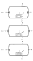
实施方式1
图2是实施方式1的无线IC器件和具备该器件的金属物件的外观立体图。金属物件60是至少表面或表面附近为金属的金属物件。FIG. 2 is an external perspective view of the wireless IC device according to
对此金属物件60的规定的面,设置无线IC器件主要部6。不将标号6称为无线IC器件是因为仅用此标号6的部分不构成无线IC器件,包含金属物件60的部分金属面后,才作为无线IC器件起作用。The wireless IC device
图3是将无线IC器件主要部放大的图。无线IC器件主要部6在绝缘基片上具备环状电极7和与该电极耦合的电磁耦合模件1。将此无线IC器件主要部6配置成环状电极7的环状面对金属物件60大致垂直。FIG. 3 is an enlarged view of main parts of the wireless IC device. The
此外,将形成环状电极7的无线IC器件主要部6,利用绝缘粘接剂装贴在金属物件60上。In addition, the
图4是概略示出使环状电极7作为发送用辅助辐射体起作用时在金属物件60上产生的电磁场分布例的图。图中的虚线表示磁场H的环路,实线表示电场E的环路。环状电极7作为磁场用辅助辐射体起作用,由环状电极7以对金属物件60的表面平行的方式产生磁场H,以对金属物件60的表面大致垂直的方式感应电场E,此电场环路感应磁场环路,其链扩展电磁场分布。FIG. 4 is a diagram schematically showing an example of the electromagnetic field distribution generated on the
上述例子中,将环状电极7作为发送用辅助辐射体进行说明,但使该电极作为接收用辅助辐射体起作用时,也得到高增益。In the above example, the
再者,图3所示电磁耦合模件1的组成部分包含后文阐述的无线IC片和馈电电路板。无线IC片与馈电电路板可连接成电导通,也可做成进行电磁场耦合。使其电磁场耦合时,在两者的连接电极之间用电介质薄膜形成电容。通过用电容使无线IC片与馈电电路板耦合,能防止无线IC片的静电造成的破坏。Furthermore, the components of the
又,使用馈电电路板的情况下,使馈电电路板的电极与环状电极7的两端进行电磁耦合。或者电磁耦合模件1可置换成单体的无线IC片。任一种情况下,都使环状电极7在直流上脱离金属物件60,因此此无线IC器件具有抗静电性高的效果。Moreover, when using a feed circuit board, the electrode of a feed circuit board and both ends of the ring-shaped
环状电极7只要配置成将电磁耦合模件1的输入输出端子之间耦合,什么样的形状都可以。The
附带说一下,金属物件表面的电场对金属物件表面垂直竖立,因此环状电极7的环状面对金属物件60的面偏离垂直时,环状电极7的磁场感应的电场强度降低,从而天线的增益降低。因此,环状电极7的环状面越对金属物件60大致垂直取向,越得到高增益,但即使环状电极7的环状面对金属物件60的面倾斜,金属物件60也作为辐射体起作用,所以可按照需要使环状电极7的环状面倾斜。Incidentally, the electric field on the surface of the metal object is vertical to the surface of the metal object, so when the ring-shaped
再者,为了将环状电极7配置成对金属物件60大致垂直,可在金属物件60的表面形成插入馈电电路板的前端部的凹部。此情况下,可在凹部的内部配置绝缘粘接剂等绝缘材料。Furthermore, in order to arrange the
又,实施方式1中,将环状电极7直接装贴在金属物件60的表面,但也可在金属箔或金属板等上装贴环状电极后,将该金属箔或金属板装贴在金属物件60上。Also, in
实施方式2Embodiment 2
图5是示出实施方式2的2个无线IC器件的组成的图。此实施方式2在高频器件的安装部与环状电极之间具备使高频器件与环状电极直接导通的匹配电路。FIG. 5 is a diagram showing the configuration of two wireless IC devices according to the second embodiment. This second embodiment includes a matching circuit for directly conducting the high-frequency device and the ring electrode between the mounting portion of the high-frequency device and the ring electrode.
图5(A)中,金属物件70是至少表面或表面附近为金属的金属物件。而且,通过将环状电极73的环状面配置成大致垂直朝向此金属物件70,使金属物件70作为辐射体起作用。In FIG. 5(A), the metal object 70 is a metal object whose surface or near the surface is metal. Furthermore, by arranging the ring-shaped surface of the ring-shaped electrode 73 to face the metal object 70 substantially vertically, the metal object 70 functions as a radiator.
在无线IC器件主要部69的内部,形成迂回曲折状的电极组成的匹配电路11和作为高频器件(电磁耦合模件或无线IC器件)的安装部的金属带部9a、9b。Inside the main part 69 of the wireless IC device, a matching circuit 11 composed of meandering electrodes and metal belt parts 9a, 9b serving as mounting parts for high frequency devices (electromagnetic coupling modules or wireless IC devices) are formed.
通过这样设置匹配电路11,能在金属带部9a、9b直接安装无线IC片。再者,将无线IC片直接安装在环状电极时,由包含匹配电路11的环状电极实质上决定无线IC器件的工作频率。By providing the matching circuit 11 in this way, the wireless IC chip can be directly mounted on the metal tape portions 9a, 9b. Furthermore, when the wireless IC chip is directly mounted on the ring-shaped electrode, the operating frequency of the wireless IC device is substantially determined by the ring-shaped electrode including the matching circuit 11 .
图5(B)示出对图5(A)所示无线IC器件主要部69的金属带部9a、9b安装电磁耦合模件1的状态。匹配电路11、作为电磁耦合模件安装部的金属带部9a、9b和环状电极73的组成,与图5(A)相同。FIG. 5(B) shows a state in which the
根据这种组成,环状电极73作为磁场用辅助辐射体起作用,与金属物件70耦合,利用与图4所示相同的作用,金属物件70作为辐射体起作用。According to this configuration, the annular electrode 73 functions as an auxiliary radiator for a magnetic field and is coupled to the metal object 70, and the metal object 70 functions as a radiator by the same function as shown in FIG. 4 .
再者,图5的金属物件70也可以是例如形成在便携电话终端的电路板上的图案电极。Furthermore, the metal object 70 in FIG. 5 may be, for example, a pattern electrode formed on a circuit board of a mobile phone terminal.
实施方式3Embodiment 3
图6是实施方式3的无线IC器件和具备该器件的金属物件的外观立体图。金属物件61是至少表面或表面附近为金属的金属物件。6 is an external perspective view of a wireless IC device according to Embodiment 3 and a metal object including the device. The
图3所示例子中,在无线IC器件主要部6的基片上设置整个环状电极,但图6所示例子在无线IC器件主要部66的基片上设置作为环状电极的一部分的环状电极71,将金属物件61的一部分兼用于环状电极。In the example shown in FIG. 3, the entire ring electrode is provided on the substrate of the
图7是图6所示无线IC器件主要部66的放大图。无线IC器件主要部66在基片上具备环状电极部71、71和与其耦合的电磁耦合模件1。关于此电磁耦合模件1的组成,与图3所示的相同。环状电极部71、71构成环状电极的一部分,将金属物件61的部分表面兼用于部分环状电极。即,利用环状电极部71、71和金属物件61的表面如图中所示那样构成环状电极。FIG. 7 is an enlarged view of a
即便是这种组成,基于环状电极部71、71和金属物件61的表面的环状电极也作为磁场用辅助辐射体起作用,并且与金属物件61耦合,利用与图4所示相同的作用,使金属物件61的表面作为辐射体起作用。Even with this composition, the annular electrode based on the
实施方式4
图8是具备实施方式4的无线IC器件的金属物件的外观图。金属物件62是例如圆柱状的金属制的罐。图2、图6所示例子中,金属物件为多面体状,但此图8所示例子中,金属物件62为圆柱状,在其侧面安装无线IC器件主要部67。FIG. 8 is an external view of a metal object including the wireless IC device according to
图9是图8所示无线IC器件主要部67的安装部分的放大图。无线IC器件主要部67具备环状电极部72、72和与其耦合的电磁耦合模件1。图7所示例子在基片上形成环状电极部71、71,但此图9的例子利用金属板形成环状电极部72、72。电磁耦合模件1的组成与图3或图7所示的相同。FIG. 9 is an enlarged view of a mounting portion of the
即便是这种组成,基于环状电极部72、72和金属物件62的表面的环状电极也作为磁场用辅助辐射体起作用,并且与金属物件62耦合,利用与图4所示相同的作用,使金属物件62的表面作为辐射体起作用。Even with this composition, the annular electrode based on the
再者,只要是导电部作为辐射体起作用的物件,它们多个重叠的情况下,所述电场和磁场的感应就在物件间链状扩展。因此,多个物件重叠(倒不如说是叠着的物件),也作为高增益的无线IC器件起作用。例如,能在使读写器的天线接近成堆应用本发明的罐装清凉饮料水的一部分的状态下,读取该成堆的全部罐装清凉饮料水的ID。Furthermore, as long as there are objects in which the conductive portion functions as a radiator, if a plurality of them overlap, the induction of the electric field and the magnetic field spreads in a chain form among the objects. Therefore, multiple objects are overlapped (or rather stacked objects) and function as a high-gain wireless IC device. For example, the IDs of all the canned soft drinks in the pile can be read in a state where the antenna of the reader/writer is brought close to a part of the canned soft drinks to which the present invention is applied in a pile.
此外,纸制的容器如果包含铝等导电层,该导电层也作为辐射体起作用。In addition, if the container made of paper contains a conductive layer such as aluminum, the conductive layer also functions as a radiator.
实施方式5
图10是具备实施方式5的无线IC器件的金属物件的外观图。图8所示例子中,在金属物件62的侧面配置电磁耦合模件1,但此图10所示例子在金属物件63的一部分设置金属带部9、9,在该金属带部9、9配置电磁耦合模件1。可在此电磁耦合模件1和金属带部9、9的周围覆盖或模塑树脂等绝缘物。FIG. 10 is an external view of a metal object including the wireless IC device according to
图11是图9所示电磁耦合模件1的安装部分的放大图。设置在部分金属物件63的金属带部9和金属物件63的一部分如图中L所示那样作为环状电极起作用。FIG. 11 is an enlarged view of a mounting portion of the
即便是这种组成,金属带部9和金属物件63的一部分也作为磁场用辅助辐射体起作用,并且与金属物件63耦合,利用与图4所示相同的作用,使金属物件63作为辐射体起作用。Even with this composition, the metal belt portion 9 and a part of the
实施方式6
图12是具备实施方式6的无线IC器件的金属物件的外观图。在此金属物件64的表面具备无线IC器件主要部68。FIG. 12 is an external view of a metal object including the wireless IC device according to
图13是此无线IC器件主要部68的放大图。无线IC器件主要部68的总体形状形成所谓折缝转位片形状,并且在绝缘片65的内表面具备粘接层,用绝缘片65将环状电极7和电磁耦合模件1夹在中间。环状电极7和电磁耦合模件1的组成与图3所示的相同。FIG. 13 is an enlarged view of the
然后,以宛如粘贴折缝转位片那样进行安装,使环状电极7对金属物件64的面垂直。Then, it is attached as if the crease index sheet is pasted so that the ring-shaped
即便是这种组成,环状电极7也作为磁场用辅助辐射体起作用,并且与金属物件64耦合,利用与图4所示相同的作用,使金属物件64作为辐射体起作用。Even with such a composition, the
再者,使沿金属物件的环路作为环状电极7起作用,但如其它实施例所示,也可使金属物件64作为环状电极的一部分起作用,并使金属物件64作为辐射体起作用。Furthermore, the loop along the metal object functions as the ring-shaped
实施方式7
图14是实施方式7的用于无线IC器件的电磁耦合模件1的外观立体图。此电磁耦合模件1也能用于其它实施方式的各无线IC器件。此电磁耦合模件1的组成部分包含无线IC片5和馈电电路板4。馈电电路板4取作为辐射体起作用的金属物件与无线IC片5之间的阻抗匹配,并作为谐振电路起作用。FIG. 14 is an external perspective view of an
图15是示出馈电电路板4的内部组成的分解图。此馈电电路板4由叠积分别形成电极图案的多个电介质层而成的多层电路板构成。在最上层的电介质层41A形成无线IC片安装用焊盘35a~35d。在电介质层41B形成与无线IC安装用焊盘35b导通的电容器电极51。在电介质层41C形成与电容器电极51之间构成电容器C1的电容器电极53。在电介质层41D~41H分别形成电感器电极45a、45b。在这些多个层都形成的电感器电极45a、45b总体上形成双螺旋状,构成相互强介电耦合的电感器L1、L2。还在电介质层41F形成与电感器L1导通的电容器电极54。将电容器电极54夹在这2个电容器电极53和55之间,形成电容器电极55。用通路孔42a~42i,使各电介质层的电极之间导通。FIG. 15 is an exploded view showing the internal composition of the
图16是包含图15所示馈电电路板4和环状电极的等效电路。图16中,电容器C1取决于图15所示电容器电极51~53之间产生的电容,电容器C2取决于图15所示电容器电极54与53、55之间产生的电容,电感器L1、L2取决于图15所示电感器电极45a、45b。FIG. 16 is an equivalent circuit including the
电容器电极55与环状电极(图3所示例子中为环状电极7)的一端平行地对置,在它们之间构成电容。电感器电极L1、L2与环状电极7的另一端部进行电磁场耦合。The
馈电电路板4中,由用电路元件L1、L2及其寄生电容构成的谐振电路,决定谐振频率。辐射电极辐射的信号的频率实质上由谐振电路的本机谐振频率决定。In the
在馈电电路板4上装载所述无线IC片5的电磁耦合模件1通过辐射电极接收未图示的读写器辐射的高频信号(例如UHF频段),并使馈电电路板4内的谐振电路谐振,仅将规定的频带的接收信号供给无线IC片5。另一方面,从该接收信号取出规定的能量,将此能量作为驱动源,使无线IC片5中存储的信息与谐振电路中规定的频率匹配后,传给辐射电极,从该辐射电极发送或传输到读写器。The
通过这样在馈电电路板内设置谐振电路,能提高频率选择性,由本机谐振频率大致决定无线IC器件的工作频率。随之,能高效率进行RFID系统中使用的频率的信号能量的收发。还能以考虑辐射体的形状和大小的方式设定最佳谐振频率,从而能提高无线ID器件的辐射特性。By arranging the resonant circuit in the feeding circuit board in this way, the frequency selectivity can be improved, and the operating frequency of the wireless IC device is roughly determined by the local resonant frequency. Accordingly, it is possible to efficiently transmit and receive signal energy of a frequency used in the RFID system. It is also possible to set an optimum resonance frequency in consideration of the shape and size of the radiator, so that the radiation characteristics of the wireless ID device can be improved.
实施方式8
图17是示出实施方式8的无线IC器件使用的电磁耦合模件的组成的图。图17中,在基体材料10的内层形成环状电极30。在此开放的2个端部30a、30b的上部,以绝缘层为中介,形成电感器电极20和电容器电极25。电感器电极20为螺旋状,其内侧的端部如后文阐述那样连接电容器电极25。FIG. 17 is a diagram showing the configuration of an electromagnetic coupling module used in the wireless IC device of
在此电感器电极20和电容器电极25的端部装载无线IC片5,如图中的放大图所示。即,在电感器电极20的端部和电容器电极25的端部分别形成无线IC片安装用焊盘35a和35b,还形成无线IC安装用焊盘35c、35d,以装载无线IC片5。The
图18是图17的II-II部分的剖视图。图18中,导线21将电感器电极20和电容器电极25连接。Fig. 18 is a sectional view of part II-II of Fig. 17 . In FIG. 18 ,
又,作为实施方式8的变换例,如图19所示,可通过阻抗匹配部8、8,使无线IC片5与环状电极30导通。In addition, as a modified example of the eighth embodiment, as shown in FIG. 19 , the
再者,也可用陶瓷等的多层基片或玻璃基片等另行制作阻抗匹配部8、8后,用导电粘接剂装贴成对环状电极30导通。Furthermore, the
实施方式9Embodiment 9
图20是实施方式9的无线IC器件的馈电电路板40的分解立体图。图21是其等效电路图。FIG. 20 is an exploded perspective view of a power
由叠积分别形成电极图案的多个电介质层而成的多层电路板,构成馈电电路板40。在最上层的电介质层41A形成无线IC片安装用焊盘35a~35d。在电介质层41B形成与无线IC安装用焊盘35b导通的电容器电极51。在电介质层41C形成与电容器电极51之间,构成电容器C1的电容器电极53。在电介质层41D~41H上,构成电感器电极45a、45b总体上形成双螺旋状的电感器L1。The power
还在电介质层41F形成与电感器L1导通的电容器电极54。将电容器电极54夹在这2个电容器电极53和55(56)之间,构成电容器电极。在电介质层41H形成与电容器电极53导通的电容器电极55。Also formed on the
电介质层41J~41N分别形成电感器电极46、47。由此电感器电极46、47构成多次卷绕的环状电极L2。用通路孔42a~42m使各电介质层之间导通。
即,此馈电电路板40正好是图15所示馈电电路板4中包含环状电极而构成的。That is, this
图21中,电容器C1取决于图20所示电容器电极51~53之间的电容,电容器C2取决于图20所示电容器电极54与53、55之间的电容,电感器L1a、L1b分别取决于图20所示电感器电极45a、45b,电感器L2取决于图20所示电感器电极46、47。In FIG. 21, the capacitor C1 depends on the capacitance between the capacitor electrodes 51-53 shown in FIG. 20, the capacitor C2 depends on the capacitance between the
实施方式10
图22是具备无线IC器件的笔记本型个人计算机的外观立体图,图23是其内部的电路板的主要部的剖视图。笔记本型个人计算机内的电路板15上,连同电子部件17、18一起安装无线IC器件主要部6,使其对电路板15大致垂直。在电路板15的上表面形成电极图案16。此电极图案16与无线IC器件主要部6耦合,作为辐射体起作用。FIG. 22 is an external perspective view of a notebook personal computer including a wireless IC device, and FIG. 23 is a cross-sectional view of a main part of an internal circuit board. On the
作为其它例,可在设置于图22所示笔记本型个人计算机内部的部件(例如液晶板)的背面的金属板上构成无线IC器件。即,可应用实施方式1~10所示无线IC器件,使所述金属板作为辐射体起作用。As another example, a wireless IC device may be formed on a metal plate provided on the back of a component (for example, a liquid crystal panel) inside a notebook personal computer shown in FIG. 22 . That is, the wireless IC devices described in
再者,除以上所示各实施方式外,只要是金属体的物件,也同样能用。例如,也能用于保险柜、天线。In addition, other than the above-described embodiments, any metal body can be used in the same way. For example, it can also be used in safes, antennas.
实施方式11Embodiment 11
图24是实施方式11的无线IC器件的主要部的剖视图。24 is a cross-sectional view of main parts of the wireless IC device according to Embodiment 11. FIG.
实施方式1在图2所示例子中,从读写器接收信号的面(金属物件60的外部的电磁波收发面)上设置无线IC器件6,但实施方式11在从读写器接收信号的面的相反面侧设置无线IC器件主要部6。In
与实施方式1的情况相同,无线IC器件主要部6也在绝缘基片上具备环状电极7和与该电极耦合的电磁耦合模件1。As in the case of the first embodiment, the
根据此组成,由来自读写器的信号(磁场Ho)在金属物件60的整个导体主面产生涡流J,此涡流在与导体主面垂直的方向产生磁场Hi。于是,环状电极7与磁场Hi耦合。由此,即使对来自无线IC器件主要部6的相反的主面的信号,也使其作为RF-ID起作用。According to this configuration, an eddy current J is generated on the entire conductor main surface of the
再者,设置无线IC器件主要部6的物件不限于金属物件,例如具有碳等导电材料的面,则同样能用。Furthermore, the object on which the
此外,环状电极可连接导体面,也可与导体面分开。In addition, the ring-shaped electrode may be connected to the conductor surface, or may be separated from the conductor surface.
实施方式12Embodiment 12
图25是实施方式12的无线IC器件的主要部的剖视图。25 is a cross-sectional view of a main part of a wireless IC device according to Embodiment 12.
实施方式1在图2所示的例子中,在金属物件60的表面(外表面),设置无线ID器件主要部6,但实施方式12在金属物件60的内部(内表面),设置无线IC器件主要部6。In
图25(A)是使金属盒(半盒)81、82的接合部往盒内伸出的图,图25(B)是使金属盒(半盒)81、82的接合部往盒外伸出的图。图25(C)是将金属盒(半盒)81、82的一端做成保持导电性的绞链结构的图。都通过橡胶衬垫等电绝缘物或电阻使接合部接合。Fig. 25 (A) is the figure that makes the junction portion of metal box (half box) 81,82 protrude in the box, and Fig. 25 (B) is the junction portion that makes metal box (half box) 81,82 stretch out toward the box out of the picture. Fig. 25(C) is a figure in which one end of the metal box (half box) 81, 82 is made into a hinge structure to maintain conductivity. In both cases, the joints are joined by electrical insulators such as rubber gaskets or resistors.
与实施方式1相同,无线IC器件主要部6也在绝缘基片上具备环状电极7和与该电极耦合的电磁耦合模件1。As in the first embodiment, the
根据此组成,由来自读写器的信号(磁场)在金属盒81、82的导体主面产生涡流,此涡流在与导体主面垂直的方向产生磁场。于是,此磁场与环状电极7耦合。由此,能作为内置RF-ID标签的金属物件进行使用。According to this configuration, eddy currents are generated on the conductor principal surfaces of the
图25(A)、(B)的例子中,使上部的金属盒82与设置无线IC器件主要部6侧的金属盒81在直流上绝缘,但电场环路和磁场环路的链沿金属盒的导体面扩展,因此上部的金属盒82侧也作为辐射体起作用。In the examples of Fig. 25(A) and (B), the
通过这样在盒内设置无线IC器件6,提高无线IC器件的耐久性和抗环境性。By arranging the
又,图25所示无线IC器件主要部6是例如设置于食品的RF-ID标签,金属盒81、82为冷藏柜、冷冻柜的壳体的情况下也相同,因此能不打开冷藏柜或冷冻柜的门而从外部读取各食品的信息。Moreover, the
又,图25所示无线IC器件主要部6是例如设置于电子部件或电路板的RF-ID标签,金属盒81、82是个人计算机或便携电话终端的壳体的情况下也相同。因此能不打开个人计算机或便携电话终端的壳体而从外部读取各电子部件和电路板的信息。The same applies when the
图25所示例子中,示出使用罐状金属盒的例子,但筒状或杯状的导体盒也能用。例如,可通过在碳柄的高尔夫球棒长柄内设置无线IC器件主要部6,作为内置能从外部读写的RF-ID标签的高尔夫球棒进行使用。In the example shown in FIG. 25, an example using a can-shaped metal case is shown, but a cylindrical or cup-shaped conductor case can also be used. For example, by providing the wireless IC device
实施方式13Embodiment 13
图26是实施方式13的无线IC器件的主要部的剖视图。26 is a cross-sectional view of a main part of a wireless IC device according to Embodiment 13.
图26的例子中,使用在表面形成电绝缘体或电阻体的被膜的金属盒83、84。其它组成与图25所示的相同。In the example of FIG. 26 ,
这样,可用盒表面的被膜使上下盒的界面为绝缘状态或大致绝缘状态。In this way, the interface between the upper and lower cases can be insulated or substantially insulated using the film on the surface of the case.
实施方式14Embodiment 14
图27是实施方式14的无线IC器件的主要部的剖视图。27 is a cross-sectional view of main parts of a wireless IC device according to Embodiment 14. FIG.
图27的例子中,在下部的金属盒85与上部的金属盒86的接合部设置凸起部94,产生间隙95。其它组成与图25所示的相同。In the example of FIG. 27 , a
这样,在金属盒的一部分存在间隙,也能利用同样的作用,作为内置RF-ID标签的金属物件进行使用。In this way, even if there is a gap in a part of the metal case, it can be used as a metal object with a built-in RF-ID tag by utilizing the same function.
实施方式15
图28是实施方式15的无线IC器件的主要部的剖视图。28 is a cross-sectional view of a main part of a wireless IC device according to
图28的例子中,在表面形成电绝缘体或电阻体的被覆的金属托盘87的内部设置无线IC器件主要部6,构成带RF-ID标签的金属托盘。此图28的例子还示出堆叠多个金属托盘的例子。In the example of FIG. 28 , the wireless IC device
通过这样叠置金属托盘,利用上述电绝缘体或电阻体的被膜,使金属托盘之间在直流上绝缘,并以金属体包围无线IC器件主要部6,但与实施方式12~14时相同,读写器能与各金属托盘的RF-ID通信。By stacking the metal trays in this way, the metal trays are insulated from each other in direct current by the coating of the above-mentioned electrical insulator or resistor, and the
实施方式16
图29是实施方式16的无线IC器件的主要部的剖视图。29 is a cross-sectional view of main parts of the wireless IC device according to the sixteenth embodiment.
图29的例子中,在边缘部形成电绝缘体或电阻体的垫环96的金属托盘88的内部设置无线IC器件主要部6,构成带RF-ID标签的金属托盘。此图29的例子还示出堆叠多个金属托盘的例子。In the example of FIG. 29 , the wireless IC device
通过这样叠置金属托盘,利用上述电绝缘体或电阻体使金属托盘之间在直流上绝缘,并以金属体包围无线IC器件主要部6,但与实施方式12~14时相同,读写器能与金属托盘的RF-ID个别通信。By stacking the metal trays in this way, the metal trays are insulated from each other in direct current by the above-mentioned electrical insulator or resistor, and the
再者,图25~图29所示例子都示出具备用电绝缘体或电阻体在直流上加以绝缘的部分,但在用导体无间隙地包围的盒或壳体的内部设置无线ID器件主要部6的情况下,虽然天线增益有些降低,但也同样能用作RF-ID标签。Furthermore, the examples shown in FIGS. 25 to 29 all show a part that is insulated on direct current with an electrical insulator or a resistor, but the main part of the wireless ID device is set inside a box or housing surrounded by a conductor without gaps. In the case of 6, although the antenna gain is somewhat reduced, it can also be used as an RF-ID tag.
以上各实施方式中使用做成矩形的环状电极,但环状电极的形状可依据收装的物件取为圆、椭圆、多边形等各种形状。还能形成在盒的底面和侧面伸展。尽管因这种形状而信号的收发面改变,也作为RF-ID起作用。In each of the above embodiments, a rectangular ring electrode is used, but the shape of the ring electrode can be various shapes such as circle, ellipse, polygon, etc. according to the objects to be stored. It is also possible to form extensions on the bottom and sides of the box. Although the signal transmission and reception surface changes due to this shape, it also functions as an RF-ID.
又,以上各实施方式中形成基于单层导体图案的环状电极,但也可做成多层线圈结构,而非单层环路。Also, in the above embodiments, ring-shaped electrodes based on a single-layer conductor pattern are formed, but a multi-layer coil structure can also be used instead of a single-layer loop.
以上各实施方式中,形成开环的环状电极,但构成环状电极与馈电电路板内的电感器磁场耦合,则环状电极也可形成闭环。即,也可构成将与环状电极的环状面平行的电感器用图案形成在馈电电路板,并使此电感器用图案与闭环的环状电极磁场耦合。In each of the above embodiments, an open-loop ring electrode is formed, but the ring electrode may form a closed loop if the ring electrode is configured to be coupled to the magnetic field of the inductor in the power feeding circuit board. That is, it is also possible to form an inductor pattern parallel to the annular surface of the annular electrode on the feed circuit board, and magnetically couple the inductor pattern to the closed-loop annular electrode.
又,以上各实施方式中,将具备环状电极的无线IC器件主要部配置成连接规定的面,但也可做成将其配置成离开面的结构,还可做成将其挂在盒的内部,离开盒的内表面(悬浮在空中)。Also, in each of the above embodiments, the main part of the wireless IC device including the annular electrode is arranged so as to be connected to a predetermined surface, but it may also be arranged so as to be separated from the surface, or may be hung on a case. Inside, away from the inner surface of the box (suspended in the air).
以上各实施方式中将具备环状电极的无线IC器件主要部配置在盒的面积大的主面,但也可将其配置在盒的侧面。In each of the above embodiments, the main part of the wireless IC device including the annular electrode is disposed on the main surface of the case having a large area, but it may also be disposed on the side of the case.
Claims (13)
Priority Applications (1)
| Application Number | Priority Date | Filing Date | Title |
|---|---|---|---|
| CN201410310158.9A CN104078767B (en) | 2007-07-09 | 2008-07-02 | Wireless IC device |
Applications Claiming Priority (7)
| Application Number | Priority Date | Filing Date | Title |
|---|---|---|---|
| JP2007179332 | 2007-07-09 | ||
| JP179332/2007 | 2007-07-09 | ||
| JP2007264603 | 2007-10-10 | ||
| JP264603/2007 | 2007-10-10 | ||
| JP2008105189 | 2008-04-14 | ||
| JP105189/2008 | 2008-04-14 | ||
| PCT/JP2008/061955 WO2009008296A1 (en) | 2007-07-09 | 2008-07-02 | Wireless ic device |
Related Child Applications (1)
| Application Number | Title | Priority Date | Filing Date |
|---|---|---|---|
| CN201410310158.9A Division CN104078767B (en) | 2007-07-09 | 2008-07-02 | Wireless IC device |
Publications (2)
| Publication Number | Publication Date |
|---|---|
| CN101542831A CN101542831A (en) | 2009-09-23 |
| CN101542831B true CN101542831B (en) | 2014-06-25 |
Family
ID=40228474
Family Applications (2)
| Application Number | Title | Priority Date | Filing Date |
|---|---|---|---|
| CN200880000689.0A Active CN101542831B (en) | 2007-07-09 | 2008-07-02 | Wireless ic device |
| CN201410310158.9A Active CN104078767B (en) | 2007-07-09 | 2008-07-02 | Wireless IC device |
Family Applications After (1)
| Application Number | Title | Priority Date | Filing Date |
|---|---|---|---|
| CN201410310158.9A Active CN104078767B (en) | 2007-07-09 | 2008-07-02 | Wireless IC device |
Country Status (6)
| Country | Link |
|---|---|
| US (2) | US8193939B2 (en) |
| EP (1) | EP2166617B1 (en) |
| JP (2) | JP4466795B2 (en) |
| KR (1) | KR101023582B1 (en) |
| CN (2) | CN101542831B (en) |
| WO (1) | WO2009008296A1 (en) |
Families Citing this family (67)
| Publication number | Priority date | Publication date | Assignee | Title |
|---|---|---|---|---|
| US7519328B2 (en) | 2006-01-19 | 2009-04-14 | Murata Manufacturing Co., Ltd. | Wireless IC device and component for wireless IC device |
| US9064198B2 (en) | 2006-04-26 | 2015-06-23 | Murata Manufacturing Co., Ltd. | Electromagnetic-coupling-module-attached article |
| US8235299B2 (en) | 2007-07-04 | 2012-08-07 | Murata Manufacturing Co., Ltd. | Wireless IC device and component for wireless IC device |
| CN101542831B (en) | 2007-07-09 | 2014-06-25 | 株式会社村田制作所 | Wireless ic device |
| KR101037035B1 (en) | 2007-07-17 | 2011-05-25 | 가부시키가이샤 무라타 세이사쿠쇼 | Wireless IC Devices and Electronics |
| CN101682113B (en) | 2007-07-18 | 2013-02-13 | 株式会社村田制作所 | Wireless ic device |
| US7830311B2 (en) * | 2007-07-18 | 2010-11-09 | Murata Manufacturing Co., Ltd. | Wireless IC device and electronic device |
| JP5267463B2 (en) | 2008-03-03 | 2013-08-21 | 株式会社村田製作所 | Wireless IC device and wireless communication system |
| EP2284949B1 (en) | 2008-05-21 | 2016-08-03 | Murata Manufacturing Co. Ltd. | Wireless ic device |
| CN104077622B (en) | 2008-05-26 | 2016-07-06 | 株式会社村田制作所 | The authenticating method of wireless IC device system and Wireless IC device |
| WO2010021217A1 (en) | 2008-08-19 | 2010-02-25 | 株式会社村田製作所 | Wireless ic device and method for manufacturing same |
| WO2010055945A1 (en) | 2008-11-17 | 2010-05-20 | 株式会社村田製作所 | Antenna and wireless ic device |
| CN102273012B (en) | 2009-01-09 | 2013-11-20 | 株式会社村田制作所 | Wireless IC device and wireless IC module |
| DE112009003613B4 (en) * | 2009-01-16 | 2020-12-17 | Murata Manufacturing Co., Ltd. | IC COMPONENT |
| CN102301528B (en) | 2009-01-30 | 2015-01-28 | 株式会社村田制作所 | Antenna and Wireless IC Devices |
| JP4796180B2 (en) * | 2009-02-23 | 2011-10-19 | 株式会社日立情報システムズ | RFID tag |
| WO2010119854A1 (en) * | 2009-04-14 | 2010-10-21 | 株式会社村田製作所 | Component for wireless ic device and wireless ic device |
| WO2010122685A1 (en) | 2009-04-21 | 2010-10-28 | 株式会社村田製作所 | Antenna apparatus and resonant frequency setting method of same |
| JP5447515B2 (en) * | 2009-06-03 | 2014-03-19 | 株式会社村田製作所 | Wireless IC device and manufacturing method thereof |
| WO2011040393A1 (en) | 2009-09-30 | 2011-04-07 | 株式会社村田製作所 | Circuit substrate and method of manufacture thereof |
| JP5304580B2 (en) | 2009-10-02 | 2013-10-02 | 株式会社村田製作所 | Wireless IC device |
| JP5418600B2 (en) | 2009-10-27 | 2014-02-19 | 株式会社村田製作所 | Transceiver and RFID tag reader |
| WO2011055703A1 (en) | 2009-11-04 | 2011-05-12 | 株式会社村田製作所 | Communication terminal and information processing system |
| GB2487315B (en) | 2009-11-04 | 2014-09-24 | Murata Manufacturing Co | Communication terminal and information processing system |
| CN102576929B (en) | 2009-11-20 | 2015-01-28 | 株式会社村田制作所 | Antenna device and mobile communication terminal |
| TWI446269B (en) * | 2009-12-03 | 2014-07-21 | Ind Tech Res Inst | Wireless communication apparatus |
| JP4978756B2 (en) | 2009-12-24 | 2012-07-18 | 株式会社村田製作所 | Communication terminal |
| WO2011108340A1 (en) | 2010-03-03 | 2011-09-09 | 株式会社村田製作所 | Wireless communication module and wireless communication device |
| JP5403146B2 (en) | 2010-03-03 | 2014-01-29 | 株式会社村田製作所 | Wireless communication device and wireless communication terminal |
| JP5477459B2 (en) * | 2010-03-12 | 2014-04-23 | 株式会社村田製作所 | Wireless communication device and metal article |
| JP5370581B2 (en) | 2010-03-24 | 2013-12-18 | 株式会社村田製作所 | RFID system |
| JP5630499B2 (en) | 2010-03-31 | 2014-11-26 | 株式会社村田製作所 | Antenna apparatus and wireless communication device |
| WO2012005278A1 (en) | 2010-07-08 | 2012-01-12 | 株式会社村田製作所 | Antenna and rfid device |
| GB2537773A (en) | 2010-07-28 | 2016-10-26 | Murata Manufacturing Co | Antenna apparatus and communication terminal instrument |
| WO2012020748A1 (en) | 2010-08-10 | 2012-02-16 | 株式会社村田製作所 | Printed wire board and wireless communication system |
| WO2012043432A1 (en) | 2010-09-30 | 2012-04-05 | 株式会社村田製作所 | Wireless ic device |
| JP5758909B2 (en) | 2010-10-12 | 2015-08-05 | 株式会社村田製作所 | Communication terminal device |
| CN102971909B (en) | 2010-10-21 | 2014-10-15 | 株式会社村田制作所 | Communication terminal device |
| CN103119785B (en) | 2011-01-05 | 2016-08-03 | 株式会社村田制作所 | wireless communication device |
| CN103299325B (en) | 2011-01-14 | 2016-03-02 | 株式会社村田制作所 | RFID chip packaging and RFID tags |
| CN103119786B (en) | 2011-02-28 | 2015-07-22 | 株式会社村田制作所 | Wireless communication device |
| WO2012121185A1 (en) | 2011-03-08 | 2012-09-13 | 株式会社村田製作所 | Antenna device and communication terminal apparatus |
| WO2012137717A1 (en) | 2011-04-05 | 2012-10-11 | 株式会社村田製作所 | Wireless communication device |
| WO2012141070A1 (en) | 2011-04-13 | 2012-10-18 | 株式会社村田製作所 | Wireless ic device and wireless communication terminal |
| JP5569648B2 (en) | 2011-05-16 | 2014-08-13 | 株式会社村田製作所 | Wireless IC device |
| WO2013008874A1 (en) | 2011-07-14 | 2013-01-17 | 株式会社村田製作所 | Wireless communication device |
| CN103370886B (en) | 2011-07-15 | 2015-05-20 | 株式会社村田制作所 | Wireless communication device |
| WO2013011865A1 (en) | 2011-07-19 | 2013-01-24 | 株式会社村田製作所 | Antenna module, antenna device, rfid tag, and communication terminal device |
| WO2013035821A1 (en) | 2011-09-09 | 2013-03-14 | 株式会社村田製作所 | Antenna device and wireless device |
| JP5904356B2 (en) * | 2011-09-12 | 2016-04-13 | 日立化成株式会社 | RFID tag and automatic recognition system |
| CN103380432B (en) | 2011-12-01 | 2016-10-19 | 株式会社村田制作所 | Wireless IC device and manufacturing method thereof |
| EP2688145A1 (en) | 2012-01-30 | 2014-01-22 | Murata Manufacturing Co., Ltd. | Wireless ic device |
| WO2013125610A1 (en) | 2012-02-24 | 2013-08-29 | 株式会社村田製作所 | Antenna device and wireless communication device |
| WO2013153697A1 (en) | 2012-04-13 | 2013-10-17 | 株式会社村田製作所 | Rfid tag inspection method, and inspection device |
| GB2539334A (en) * | 2012-10-26 | 2016-12-14 | Murata Manufacturing Co | Interface, communication apparatus, and program |
| US11354558B2 (en) | 2013-01-18 | 2022-06-07 | Amatech Group Limited | Contactless smartcards with coupling frames |
| US9992884B2 (en) | 2013-10-19 | 2018-06-05 | Armani Williams | Phone and tablet case |
| DE112015000479T5 (en) * | 2014-01-23 | 2016-11-10 | Murata Manufacturing Co., Ltd. | Article with wireless communication identifier and wireless communication identifier |
| GB2539839B8 (en) * | 2014-04-28 | 2021-07-07 | Murata Manufacturing Co | Wireless IC device, clip-shaped RFID tag, and article having RFID tag |
| JP2015225579A (en) * | 2014-05-29 | 2015-12-14 | 株式会社村田製作所 | Wireless IC device, manufacturing method thereof, and article with wireless IC device |
| CN105875431B (en) * | 2016-04-19 | 2019-03-08 | 福州市佳璞电子商务有限公司 | RFID transceiver, the small-sized livestock and poultry based on RFID transceiver flock together alarm system and alarm method |
| WO2018092583A1 (en) | 2016-11-15 | 2018-05-24 | 株式会社村田製作所 | Uhf-band rfid tag and uhf-band rfid-tagged article |
| US10373045B2 (en) | 2016-12-01 | 2019-08-06 | Avery Dennison Retail Information Services, Llc | Coupling of RFID straps to antennae using a combination of magnetic and electric fields |
| JP7075729B2 (en) * | 2017-06-28 | 2022-05-26 | 株式会社ユニバーサルエンターテインメント | Non-contact information medium and its manufacturing method |
| WO2019124196A1 (en) * | 2017-12-20 | 2019-06-27 | 愛知製鋼株式会社 | Magnetic marker and magnetic marker system |
| JP6912024B1 (en) * | 2019-09-05 | 2021-07-28 | 株式会社村田製作所 | Medical metal device with wireless IC tag |
| CN117015944A (en) * | 2021-03-26 | 2023-11-07 | 索尼集团公司 | Communication system and communication method |
Citations (4)
| Publication number | Priority date | Publication date | Assignee | Title |
|---|---|---|---|---|
| US6249258B1 (en) * | 1995-09-15 | 2001-06-19 | Aeg Identifikationssysteme | Transponder arrangement |
| EP1280232A1 (en) * | 2001-07-27 | 2003-01-29 | TDK Corporation | Antenna device capable of being commonly used at a plurality of frequencies and electronic equipment having the same |
| US6812707B2 (en) * | 2001-11-27 | 2004-11-02 | Mitsubishi Materials Corporation | Detection element for objects and detection device using the same |
| US7088249B2 (en) * | 2000-07-19 | 2006-08-08 | Hanex Co., Ltd. | Housing structure for RFID tag, installation structure for RFID tag, and communication using such RFID tag |
Family Cites Families (406)
| Publication number | Priority date | Publication date | Assignee | Title |
|---|---|---|---|---|
| US3364564A (en) | 1965-06-28 | 1968-01-23 | Gregory Ind Inc | Method of producing welding studs dischargeable in end-to-end relationship |
| JPS5754964B2 (en) | 1974-05-08 | 1982-11-20 | ||
| JPS6193701A (en) | 1984-10-13 | 1986-05-12 | Toyota Motor Corp | Antenna system for automobile |
| JPS62127140U (en) | 1986-02-03 | 1987-08-12 | ||
| US5253969A (en) | 1989-03-10 | 1993-10-19 | Sms Schloemann-Siemag Aktiengesellschaft | Feeding system for strip material, particularly in treatment plants for metal strips |
| JP2763664B2 (en) | 1990-07-25 | 1998-06-11 | 日本碍子株式会社 | Wiring board for distributed constant circuit |
| NL9100176A (en) | 1991-02-01 | 1992-03-02 | Nedap Nv | Antenna configuration for contactless identification label - forms part of tuned circuit of ID or credit card interrogated via inductive coupling |
| NL9100347A (en) | 1991-02-26 | 1992-03-02 | Nedap Nv | Integrated transformer circuit for ID or credit card - is interrogated via contactless inductive coupling using capacitor to form tuned circuit |
| JPH04321190A (en) | 1991-04-22 | 1992-11-11 | Mitsubishi Electric Corp | Antenna circuit and its production for non-contact type portable storage |
| EP0522806B1 (en) | 1991-07-08 | 1996-11-20 | Nippon Telegraph And Telephone Corporation | Retractable antenna system |
| JPH05327331A (en) | 1992-05-15 | 1993-12-10 | Matsushita Electric Works Ltd | Printed antenna |
| JP3186235B2 (en) | 1992-07-30 | 2001-07-11 | 株式会社村田製作所 | Resonator antenna |
| JPH0677729A (en) | 1992-08-25 | 1994-03-18 | Mitsubishi Electric Corp | Antenna integrated microwave circuit |
| JPH06177635A (en) | 1992-12-07 | 1994-06-24 | Mitsubishi Electric Corp | Cross dipole antenna system |
| JPH07183836A (en) | 1993-12-22 | 1995-07-21 | San'eisha Mfg Co Ltd | Coupling filter device for distribution line carrier communication |
| US5491483A (en) | 1994-01-05 | 1996-02-13 | Texas Instruments Incorporated | Single loop transponder system and method |
| US6096431A (en) | 1994-07-25 | 2000-08-01 | Toppan Printing Co., Ltd. | Biodegradable cards |
| JP3141692B2 (en) | 1994-08-11 | 2001-03-05 | 松下電器産業株式会社 | Millimeter wave detector |
| DE4431754C1 (en) | 1994-09-06 | 1995-11-23 | Siemens Ag | Carrier element for ic module of chip card |
| US5528222A (en) | 1994-09-09 | 1996-06-18 | International Business Machines Corporation | Radio frequency circuit and memory in thin flexible package |
| JPH0887580A (en) | 1994-09-14 | 1996-04-02 | Omron Corp | Data carriers and ball games |
| JP2837829B2 (en) | 1995-03-31 | 1998-12-16 | 松下電器産業株式会社 | Inspection method for semiconductor device |
| JPH08279027A (en) | 1995-04-04 | 1996-10-22 | Toshiba Corp | Wireless communication card |
| US5955723A (en) | 1995-05-03 | 1999-09-21 | Siemens Aktiengesellschaft | Contactless chip card |
| JPH08307126A (en) | 1995-05-09 | 1996-11-22 | Kyocera Corp | Antenna storage structure |
| JP3637982B2 (en) | 1995-06-27 | 2005-04-13 | 株式会社荏原電産 | Inverter-driven pump control system |
| US5629241A (en) | 1995-07-07 | 1997-05-13 | Hughes Aircraft Company | Microwave/millimeter wave circuit structure with discrete flip-chip mounted elements, and method of fabricating the same |
| JP3150575B2 (en) | 1995-07-18 | 2001-03-26 | 沖電気工業株式会社 | Tag device and manufacturing method thereof |
| GB2305075A (en) | 1995-09-05 | 1997-03-26 | Ibm | Radio Frequency Tag for Electronic Apparatus |
| US6104611A (en) * | 1995-10-05 | 2000-08-15 | Nortel Networks Corporation | Packaging system for thermally controlling the temperature of electronic equipment |
| JP3882218B2 (en) | 1996-03-04 | 2007-02-14 | ソニー株式会社 | optical disk |
| JP3471160B2 (en) | 1996-03-18 | 2003-11-25 | 株式会社東芝 | Monolithic antenna |
| JPH09270623A (en) | 1996-03-29 | 1997-10-14 | Murata Mfg Co Ltd | Antenna system |
| AUPO055296A0 (en) | 1996-06-19 | 1996-07-11 | Integrated Silicon Design Pty Ltd | Enhanced range transponder system |
| US6104311A (en) | 1996-08-26 | 2000-08-15 | Addison Technologies | Information storage and identification tag |
| JP2001505682A (en) | 1996-10-09 | 2001-04-24 | ペーアーファウ カード ゲームベーハ | Smart card manufacturing method and connection arrangement for manufacturing |
| JPH10171954A (en) | 1996-12-05 | 1998-06-26 | Hitachi Maxell Ltd | Non-contact IC card |
| JP3279205B2 (en) | 1996-12-10 | 2002-04-30 | 株式会社村田製作所 | Surface mount antenna and communication equipment |
| JPH10193849A (en) | 1996-12-27 | 1998-07-28 | Rohm Co Ltd | Circuit chip mounted card and circuit chip module |
| DE19703029A1 (en) | 1997-01-28 | 1998-07-30 | Amatech Gmbh & Co Kg | Transmission module for a transponder device and transponder device and method for operating a transponder device |
| US6181287B1 (en) | 1997-03-10 | 2001-01-30 | Precision Dynamics Corporation | Reactively coupled elements in circuits on flexible substrates |
| JPH10293828A (en) | 1997-04-18 | 1998-11-04 | Omron Corp | Data carrier, coil module, reader / writer, and clothing data acquisition method |
| EP1031939B1 (en) | 1997-11-14 | 2005-09-14 | Toppan Printing Co., Ltd. | Composite ic card |
| JP3800765B2 (en) | 1997-11-14 | 2006-07-26 | 凸版印刷株式会社 | Compound IC card |
| JP2001084463A (en) | 1999-09-14 | 2001-03-30 | Miyake:Kk | Resonance circuit |
| JPH11261325A (en) | 1998-03-10 | 1999-09-24 | Shiro Sugimura | Coil element and manufacturing method thereof |
| US6320509B1 (en) * | 1998-03-16 | 2001-11-20 | Intermec Ip Corp. | Radio frequency identification transponder having a high gain antenna configuration |
| EP0987789A4 (en) | 1998-03-31 | 2004-09-22 | Matsushita Electric Industrial Co Ltd | ANTENNA AND DIGITAL TELEVISION |
| JP4260917B2 (en) | 1998-03-31 | 2009-04-30 | 株式会社東芝 | Loop antenna |
| US5936150A (en) | 1998-04-13 | 1999-08-10 | Rockwell Science Center, Llc | Thin film resonant chemical sensor with resonant acoustic isolator |
| CN1267267A (en) | 1998-04-14 | 2000-09-20 | 德克萨斯黎伯迪纸板箱公司 | Container for compressors and other goods |
| US6018299A (en) | 1998-06-09 | 2000-01-25 | Motorola, Inc. | Radio frequency identification tag having a printed antenna and method |
| US6107920A (en) | 1998-06-09 | 2000-08-22 | Motorola, Inc. | Radio frequency identification tag having an article integrated antenna |
| JP2000021639A (en) | 1998-07-02 | 2000-01-21 | Sharp Corp | Inductor, resonance circuit, matching circuit, antenna circuit and oscillation circuit using the same |
| JP2000022421A (en) | 1998-07-03 | 2000-01-21 | Murata Mfg Co Ltd | Chip antenna and radio device mounted with it |
| AUPP473898A0 (en) | 1998-07-20 | 1998-08-13 | Integrated Silicon Design Pty Ltd | Metal screened electronic labelling system |
| EP0977145A3 (en) | 1998-07-28 | 2002-11-06 | Kabushiki Kaisha Toshiba | Radio IC card |
| JP2000311226A (en) | 1998-07-28 | 2000-11-07 | Toshiba Corp | Wireless IC card, manufacturing method thereof, and wireless IC card read / write system |
| JP2000059260A (en) | 1998-08-04 | 2000-02-25 | Sony Corp | Storage device |
| CA2338522C (en) | 1998-08-14 | 2009-04-07 | 3M Innovative Properties Company | Radio frequency identification systems applications |
| AU762495B2 (en) | 1998-08-14 | 2003-06-26 | 3M Innovative Properties Company | Application for a radio frequency identification system |
| JP4411670B2 (en) | 1998-09-08 | 2010-02-10 | 凸版印刷株式会社 | Non-contact IC card manufacturing method |
| JP4508301B2 (en) | 1998-09-16 | 2010-07-21 | 大日本印刷株式会社 | Non-contact IC card |
| JP3513033B2 (en) * | 1998-10-16 | 2004-03-31 | 三菱電機株式会社 | Multi-frequency antenna system |
| JP3632466B2 (en) | 1998-10-23 | 2005-03-23 | 凸版印刷株式会社 | Inspection device and inspection method for non-contact IC card |
| JP2000137779A (en) | 1998-10-30 | 2000-05-16 | Hitachi Maxell Ltd | Non-contact information medium and its manufacturing method |
| US6837438B1 (en) | 1998-10-30 | 2005-01-04 | Hitachi Maxell, Ltd. | Non-contact information medium and communication system utilizing the same |
| JP3924962B2 (en) | 1998-10-30 | 2007-06-06 | 株式会社デンソー | ID tag for dishes |
| JP2000137785A (en) | 1998-10-30 | 2000-05-16 | Sony Corp | Method of manufacturing non-contact type IC card and non-contact type IC card |
| JP2000148948A (en) | 1998-11-05 | 2000-05-30 | Sony Corp | Non-contact type IC label and manufacturing method thereof |
| JP2000172812A (en) | 1998-12-08 | 2000-06-23 | Hitachi Maxell Ltd | Noncontact information medium |
| FR2787640B1 (en) | 1998-12-22 | 2003-02-14 | Gemplus Card Int | ARRANGEMENT OF AN ANTENNA IN A METALLIC ENVIRONMENT |
| JP3088404B2 (en) | 1999-01-14 | 2000-09-18 | 埼玉日本電気株式会社 | Mobile radio terminal and built-in antenna |
| JP2000222540A (en) | 1999-02-03 | 2000-08-11 | Hitachi Maxell Ltd | Non-contact type semiconductor tag |
| JP2000228602A (en) | 1999-02-08 | 2000-08-15 | Alps Electric Co Ltd | Resonance line |
| JP2000243797A (en) | 1999-02-18 | 2000-09-08 | Sanken Electric Co Ltd | Semiconductor wafer, and cutting method thereof, and semiconductor wafer assembly and cutting method thereof |
| JP3967487B2 (en) | 1999-02-23 | 2007-08-29 | 株式会社東芝 | IC card |
| JP2000251049A (en) | 1999-03-03 | 2000-09-14 | Konica Corp | Card and production thereof |
| JP4106673B2 (en) | 1999-03-05 | 2008-06-25 | 株式会社エフ・イー・シー | Antenna device using coil unit, printed circuit board |
| JP4349597B2 (en) | 1999-03-26 | 2009-10-21 | 大日本印刷株式会社 | IC chip manufacturing method and memory medium manufacturing method incorporating the same |
| JP2000286634A (en) | 1999-03-30 | 2000-10-13 | Ngk Insulators Ltd | Antenna system and its manufacture |
| JP3751178B2 (en) | 1999-03-30 | 2006-03-01 | 日本碍子株式会社 | Transceiver |
| US6542050B1 (en) | 1999-03-30 | 2003-04-01 | Ngk Insulators, Ltd. | Transmitter-receiver |
| JP3067764B1 (en) | 1999-03-31 | 2000-07-24 | 株式会社豊田自動織機製作所 | Mobile communication coupler, mobile body, and mobile communication method |
| JP2000321984A (en) | 1999-05-12 | 2000-11-24 | Hitachi Ltd | Label with RF-ID tag |
| JP3557130B2 (en) | 1999-07-14 | 2004-08-25 | 新光電気工業株式会社 | Method for manufacturing semiconductor device |
| JP2001043340A (en) | 1999-07-29 | 2001-02-16 | Toppan Printing Co Ltd | Composite IC card |
| US6259369B1 (en) | 1999-09-30 | 2001-07-10 | Moore North America, Inc. | Low cost long distance RFID reading |
| JP2001101369A (en) | 1999-10-01 | 2001-04-13 | Matsushita Electric Ind Co Ltd | RF tag |
| JP3451373B2 (en) | 1999-11-24 | 2003-09-29 | オムロン株式会社 | Manufacturing method of data carrier capable of reading electromagnetic wave |
| JP4186149B2 (en) | 1999-12-06 | 2008-11-26 | 株式会社エフ・イー・シー | Auxiliary antenna for IC card |
| JP2001188890A (en) | 2000-01-05 | 2001-07-10 | Omron Corp | Non-contact tag |
| JP2001240046A (en) | 2000-02-25 | 2001-09-04 | Toppan Forms Co Ltd | Container and manufacturing method thereof |
| KR20000024634A (en) * | 2000-02-25 | 2000-05-06 | 신기영 | Ultra-thin wideband micro strip patch antennas |
| JP4514880B2 (en) | 2000-02-28 | 2010-07-28 | 大日本印刷株式会社 | Book delivery, returns and inventory management system |
| JP2001257292A (en) | 2000-03-10 | 2001-09-21 | Hitachi Maxell Ltd | Semiconductor device |
| JP2001256457A (en) | 2000-03-13 | 2001-09-21 | Toshiba Corp | Semiconductor device, manufacturing method thereof, and IC card communication system |
| JP2003529163A (en) | 2000-03-28 | 2003-09-30 | ルカトロン アーゲー | RFID label having member for adjusting resonance frequency |
| JP4624536B2 (en) | 2000-04-04 | 2011-02-02 | 大日本印刷株式会社 | Non-contact data carrier device |
| JP4624537B2 (en) * | 2000-04-04 | 2011-02-02 | 大日本印刷株式会社 | Non-contact data carrier device, storage |
| JP2001291181A (en) | 2000-04-07 | 2001-10-19 | Ricoh Elemex Corp | Sensor and sensor system |
| JP2001319380A (en) | 2000-05-11 | 2001-11-16 | Mitsubishi Materials Corp | Optical disk with RFID |
| JP2001331976A (en) | 2000-05-17 | 2001-11-30 | Casio Comput Co Ltd | Optical recording type recording medium |
| JP4223174B2 (en) | 2000-05-19 | 2009-02-12 | Dxアンテナ株式会社 | Film antenna |
| JP2001339226A (en) | 2000-05-26 | 2001-12-07 | Nec Saitama Ltd | Antenna system |
| JP2001344574A (en) | 2000-05-30 | 2001-12-14 | Mitsubishi Materials Corp | Interrogator antenna device |
| JP2001352176A (en) | 2000-06-05 | 2001-12-21 | Fuji Xerox Co Ltd | Multilayer printed wiring board and manufacturing method of multilayer printed wiring board |
| AU2001275117A1 (en) | 2000-06-06 | 2001-12-17 | Battelle Memorial Institute | Remote communication system and method |
| JP2001358527A (en) | 2000-06-12 | 2001-12-26 | Matsushita Electric Ind Co Ltd | Antenna device |
| DE60107500T2 (en) | 2000-06-23 | 2005-04-07 | Toyo Aluminium K.K. | Antenna coil for smart cards and manufacturing processes |
| JP2002157564A (en) | 2000-11-21 | 2002-05-31 | Toyo Aluminium Kk | Antenna coil for ic card and its manufacturing method |
| AU775854B2 (en) | 2000-07-04 | 2004-08-19 | Credipass Co., Ltd. | Passive transponder identification system and credit-card type transponder |
| JP4138211B2 (en) | 2000-07-06 | 2008-08-27 | 株式会社村田製作所 | Electronic component and manufacturing method thereof, collective electronic component, mounting structure of electronic component, and electronic apparatus |
| JP2002024776A (en) | 2000-07-07 | 2002-01-25 | Nippon Signal Co Ltd:The | Ic card reader/writer |
| RU2163739C1 (en) | 2000-07-20 | 2001-02-27 | Криштопов Александр Владимирович | Antenna |
| JP2002042076A (en) | 2000-07-21 | 2002-02-08 | Dainippon Printing Co Ltd | Non-contact data carrier and booklet having non-contact data carrier |
| JP3075400U (en) | 2000-08-03 | 2001-02-16 | 昌栄印刷株式会社 | Non-contact IC card |
| JP2002063557A (en) | 2000-08-21 | 2002-02-28 | Mitsubishi Materials Corp | Tag for rfid |
| JP2002076750A (en) | 2000-08-24 | 2002-03-15 | Murata Mfg Co Ltd | Antenna device and radio equipment equipped with it |
| JP3481575B2 (en) | 2000-09-28 | 2003-12-22 | 寛児 川上 | antenna |
| JP4615695B2 (en) | 2000-10-19 | 2011-01-19 | 三星エスディーエス株式会社 | IC module for IC card and IC card using it |
| US6634564B2 (en) | 2000-10-24 | 2003-10-21 | Dai Nippon Printing Co., Ltd. | Contact/noncontact type data carrier module |
| JP4628611B2 (en) | 2000-10-27 | 2011-02-09 | 三菱マテリアル株式会社 | antenna |
| JP4432254B2 (en) | 2000-11-20 | 2010-03-17 | 株式会社村田製作所 | Surface mount antenna structure and communication device including the same |
| JP2002185358A (en) | 2000-11-24 | 2002-06-28 | Supersensor Pty Ltd | Method for fitting rf transponder to container |
| JP4641096B2 (en) | 2000-12-07 | 2011-03-02 | 大日本印刷株式会社 | Non-contact data carrier device and wiring member for booster antenna |
| JP2002183676A (en) | 2000-12-08 | 2002-06-28 | Hitachi Ltd | Information reading device |
| JP2002183690A (en) | 2000-12-11 | 2002-06-28 | Hitachi Maxell Ltd | Non-contact IC tag device |
| EP1350233A4 (en) | 2000-12-15 | 2005-04-13 | Electrox Corp | METHOD FOR MANUFACTURING NEW RADIO FREQUENCY IDENTIFICATION DEVICES AT LOW PRICES |
| JP3788325B2 (en) | 2000-12-19 | 2006-06-21 | 株式会社村田製作所 | Multilayer coil component and manufacturing method thereof |
| TW531976B (en) | 2001-01-11 | 2003-05-11 | Hanex Co Ltd | Communication apparatus and installing structure, manufacturing method and communication method |
| JP3621655B2 (en) | 2001-04-23 | 2005-02-16 | 株式会社ハネックス中央研究所 | RFID tag structure and manufacturing method thereof |
| JP2002280821A (en) | 2001-01-12 | 2002-09-27 | Furukawa Electric Co Ltd:The | Antenna device and terminal equipment |
| KR20020061103A (en) | 2001-01-12 | 2002-07-22 | 후루까와덴끼고오교 가부시끼가이샤 | Antenna device and terminal with the antenna device |
| JP2002232221A (en) | 2001-01-30 | 2002-08-16 | Alps Electric Co Ltd | Transmission and reception unit |
| JPWO2002061675A1 (en) | 2001-01-31 | 2004-06-03 | 株式会社ルネサステクノロジ | Non-contact identification medium |
| JP4662400B2 (en) | 2001-02-05 | 2011-03-30 | 大日本印刷株式会社 | Articles with coil-on-chip semiconductor modules |
| JP2002246828A (en) | 2001-02-15 | 2002-08-30 | Mitsubishi Materials Corp | Transponder antenna |
| DE60239262D1 (en) | 2001-03-02 | 2011-04-07 | Nxp Bv | MODULE AND ELECTRONIC DEVICE |
| JP4712986B2 (en) | 2001-03-06 | 2011-06-29 | 大日本印刷株式会社 | Liquid container with RFID tag |
| JP2002298109A (en) | 2001-03-30 | 2002-10-11 | Toppan Forms Co Ltd | Non-contact IC media and method of manufacturing the same |
| JP3772778B2 (en) | 2001-03-30 | 2006-05-10 | 三菱マテリアル株式会社 | Antenna coil, identification tag using the same, reader / writer device, reader device and writer device |
| JP3570386B2 (en) | 2001-03-30 | 2004-09-29 | 松下電器産業株式会社 | Portable information terminal with built-in wireless function |
| JP2002308437A (en) | 2001-04-16 | 2002-10-23 | Dainippon Printing Co Ltd | Inspection system using RFID tag |
| JP2002319812A (en) | 2001-04-20 | 2002-10-31 | Oji Paper Co Ltd | Data carrier attachment method |
| JP4700831B2 (en) | 2001-04-23 | 2011-06-15 | 株式会社ハネックス | RFID tag communication distance expansion method |
| JP2005236339A (en) | 2001-07-19 | 2005-09-02 | Oji Paper Co Ltd | IC chip assembly |
| FI112550B (en) | 2001-05-31 | 2003-12-15 | Rafsec Oy | Smart label and smart label path |
| JP2002362613A (en) | 2001-06-07 | 2002-12-18 | Toppan Printing Co Ltd | Laminated packaging material in which non-contact IC is laminated, packaging container using the same, and method for detecting opening of packaging container |
| JP2002366917A (en) | 2001-06-07 | 2002-12-20 | Hitachi Ltd | IC card with built-in antenna |
| JP4710174B2 (en) | 2001-06-13 | 2011-06-29 | 株式会社村田製作所 | Balanced LC filter |
| JP2002373029A (en) | 2001-06-18 | 2002-12-26 | Hitachi Ltd | How to prevent unauthorized copying of software using IC tags |
| JP4882167B2 (en) | 2001-06-18 | 2012-02-22 | 大日本印刷株式会社 | Card-integrated form with non-contact IC chip |
| JP4759854B2 (en) | 2001-06-19 | 2011-08-31 | 株式会社寺岡精工 | Mounting method of IC tag to metal object and IC tag built-in marker |
| JP2003087008A (en) | 2001-07-02 | 2003-03-20 | Ngk Insulators Ltd | Multilayer dielectric filter |
| JP4058919B2 (en) | 2001-07-03 | 2008-03-12 | 日立化成工業株式会社 | Non-contact IC label, non-contact IC card, non-contact IC label or IC module for non-contact IC card |
| JP2003026177A (en) | 2001-07-12 | 2003-01-29 | Toppan Printing Co Ltd | Non-contact package with IC chip |
| JP2003030612A (en) | 2001-07-19 | 2003-01-31 | Oji Paper Co Ltd | Ic chip mounting body |
| JP4670195B2 (en) | 2001-07-23 | 2011-04-13 | 凸版印刷株式会社 | Mobile phone case with non-contact IC card |
| ATE377908T1 (en) | 2001-07-26 | 2007-11-15 | Irdeto Access Bv | TIME VALIDATION SYSTEM |
| US6407920B1 (en) * | 2001-07-30 | 2002-06-18 | Delta Electronics, Inc. | Heat-dissipating assembly and process for assembling the same |
| JP2003069335A (en) * | 2001-08-28 | 2003-03-07 | Hitachi Kokusai Electric Inc | Auxiliary antenna |
| JP2003067711A (en) | 2001-08-29 | 2003-03-07 | Toppan Forms Co Ltd | Articles with IC chip mounting or antenna part |
| JP2003078336A (en) | 2001-08-30 | 2003-03-14 | Tokai Univ | Stacked spiral antenna |
| JP2003078333A (en) | 2001-08-30 | 2003-03-14 | Murata Mfg Co Ltd | Radio communication apparatus |
| JP4514374B2 (en) | 2001-09-05 | 2010-07-28 | トッパン・フォームズ株式会社 | RF-ID inspection system |
| JP4747467B2 (en) | 2001-09-07 | 2011-08-17 | 大日本印刷株式会社 | Non-contact IC tag |
| JP2003085520A (en) | 2001-09-11 | 2003-03-20 | Oji Paper Co Ltd | IC card manufacturing method |
| JP2003099184A (en) | 2001-09-25 | 2003-04-04 | Sharp Corp | Information processing system, information processing device and input pen used therein |
| JP4845306B2 (en) | 2001-09-25 | 2011-12-28 | トッパン・フォームズ株式会社 | RF-ID inspection system |
| JP4698096B2 (en) | 2001-09-25 | 2011-06-08 | トッパン・フォームズ株式会社 | RF-ID inspection system |
| JP2003110344A (en) | 2001-09-26 | 2003-04-11 | Hitachi Metals Ltd | Surface-mounting type antenna and antenna device mounting the same |
| JP2003132330A (en) | 2001-10-25 | 2003-05-09 | Sato Corp | RFID label printer |
| JP2003134007A (en) | 2001-10-30 | 2003-05-09 | Auto Network Gijutsu Kenkyusho:Kk | Signal transmission / reception system between vehicle-mounted devices and signal transmission / reception method between vehicle-mounted devices |
| JP3908514B2 (en) | 2001-11-20 | 2007-04-25 | 大日本印刷株式会社 | Package with IC tag and method of manufacturing package with IC tag |
| JP3984458B2 (en) | 2001-11-20 | 2007-10-03 | 大日本印刷株式会社 | Manufacturing method of package with IC tag |
| JP3894540B2 (en) | 2001-11-30 | 2007-03-22 | トッパン・フォームズ株式会社 | Interposer with conductive connection |
| JP2003188338A (en) | 2001-12-13 | 2003-07-04 | Sony Corp | Circuit board device and method of manufacturing the same |
| JP3700777B2 (en) | 2001-12-17 | 2005-09-28 | 三菱マテリアル株式会社 | Electrode structure of RFID tag and method for adjusting resonance frequency using the electrode |
| JP2003188620A (en) | 2001-12-19 | 2003-07-04 | Murata Mfg Co Ltd | Module integrated antenna |
| JP4028224B2 (en) | 2001-12-20 | 2007-12-26 | 大日本印刷株式会社 | Paper IC card substrate having non-contact communication function |
| JP3895175B2 (en) | 2001-12-28 | 2007-03-22 | Ntn株式会社 | Dielectric resin integrated antenna |
| JP2003209421A (en) | 2002-01-17 | 2003-07-25 | Dainippon Printing Co Ltd | RFID tag having transparent antenna and method of manufacturing the same |
| JP3915092B2 (en) | 2002-01-21 | 2007-05-16 | 株式会社エフ・イー・シー | Booster antenna for IC card |
| JP2003216919A (en) * | 2002-01-23 | 2003-07-31 | Toppan Forms Co Ltd | RF-ID media |
| JP2003233780A (en) | 2002-02-06 | 2003-08-22 | Mitsubishi Electric Corp | Data communication device |
| JP3998992B2 (en) | 2002-02-14 | 2007-10-31 | 大日本印刷株式会社 | Method for forming antenna pattern on IC chip mounted on web and package with IC tag |
| JP2003243918A (en) | 2002-02-18 | 2003-08-29 | Dainippon Printing Co Ltd | Non-contact IC tag antenna and non-contact IC tag |
| JP2003249813A (en) * | 2002-02-25 | 2003-09-05 | Tecdia Kk | RFID tag with loop antenna |
| US7119693B1 (en) | 2002-03-13 | 2006-10-10 | Celis Semiconductor Corp. | Integrated circuit with enhanced coupling |
| JP2003288560A (en) | 2002-03-27 | 2003-10-10 | Toppan Forms Co Ltd | Interposer and inlet sheet having antistatic function |
| US7129834B2 (en) | 2002-03-28 | 2006-10-31 | Kabushiki Kaisha Toshiba | String wireless sensor and its manufacturing method |
| JP2003309418A (en) | 2002-04-17 | 2003-10-31 | Alps Electric Co Ltd | Dipole antenna |
| JP2003317060A (en) | 2002-04-22 | 2003-11-07 | Dainippon Printing Co Ltd | IC card |
| JP2003317052A (en) | 2002-04-24 | 2003-11-07 | Smart Card:Kk | Ic tag system |
| JP3879098B2 (en) | 2002-05-10 | 2007-02-07 | 株式会社エフ・イー・シー | Booster antenna for IC card |
| JP3979178B2 (en) | 2002-05-14 | 2007-09-19 | 凸版印刷株式会社 | Non-contact IC medium module and non-contact IC medium |
| US6753814B2 (en) | 2002-06-27 | 2004-06-22 | Harris Corporation | Dipole arrangements using dielectric substrates of meta-materials |
| US7097758B2 (en) * | 2002-07-03 | 2006-08-29 | Exxonmobil Chemical Patents Inc. | Converting mist flow to annular flow in thermal cracking application |
| JP3863464B2 (en) | 2002-07-05 | 2006-12-27 | 株式会社ヨコオ | Filter built-in antenna |
| JP3803085B2 (en) | 2002-08-08 | 2006-08-02 | 株式会社日立製作所 | Wireless IC tag |
| JP4107381B2 (en) | 2002-08-23 | 2008-06-25 | 横浜ゴム株式会社 | Pneumatic tire |
| JP2004096566A (en) | 2002-09-02 | 2004-03-25 | Toenec Corp | Inductive communication equipment |
| JP3925364B2 (en) | 2002-09-03 | 2007-06-06 | 株式会社豊田中央研究所 | Antenna and diversity receiver |
| GB2393076A (en) * | 2002-09-12 | 2004-03-17 | Rf Tags Ltd | Radio frequency identification tag which has a ground plane not substantially larger than the area spanned by the patch antenna |
| DE10393263T5 (en) | 2002-09-20 | 2005-09-15 | Fairchild Semiconductor Corp. | A high bandwidth logarithmic helix antenna method and system for a radio frequency identification tagging system |
| JP2004126750A (en) | 2002-09-30 | 2004-04-22 | Toppan Forms Co Ltd | Information writing / reading device, antenna and RF-ID medium |
| JP3958667B2 (en) * | 2002-10-16 | 2007-08-15 | 株式会社日立国際電気 | Loop antenna for reader / writer, and article management shelf and book management system provided with the loop antenna |
| JP2006503504A (en) | 2002-10-17 | 2006-01-26 | アンビエント・コーポレイション | Data combiner configuration for power line communication. |
| JP3659956B2 (en) | 2002-11-11 | 2005-06-15 | 松下電器産業株式会社 | Pressure measuring device and pressure measuring system |
| JP2004213582A (en) | 2003-01-09 | 2004-07-29 | Mitsubishi Materials Corp | RFID tag and reader / writer and RFID system provided with the tag |
| JP2004234595A (en) | 2003-02-03 | 2004-08-19 | Matsushita Electric Ind Co Ltd | Information recording medium reader |
| EP1594188B1 (en) | 2003-02-03 | 2010-04-14 | Panasonic Corporation | Antenna device and wireless communication device using same |
| EP1445821A1 (en) | 2003-02-06 | 2004-08-11 | Matsushita Electric Industrial Co., Ltd. | Portable radio communication apparatus provided with a boom portion |
| US7225992B2 (en) | 2003-02-13 | 2007-06-05 | Avery Dennison Corporation | RFID device tester and method |
| JP2004253858A (en) | 2003-02-18 | 2004-09-09 | Minerva:Kk | Booster antenna device for ic tag |
| JP2004280390A (en) | 2003-03-14 | 2004-10-07 | Toppan Forms Co Ltd | RF-ID media and method for manufacturing RF-ID media |
| JP4010263B2 (en) | 2003-03-14 | 2007-11-21 | 富士電機ホールディングス株式会社 | Antenna and data reader |
| JP4034676B2 (en) | 2003-03-20 | 2008-01-16 | 日立マクセル株式会社 | Non-contact communication type information carrier |
| JP4097139B2 (en) | 2003-03-26 | 2008-06-11 | Necトーキン株式会社 | Wireless tag |
| JP2004297249A (en) | 2003-03-26 | 2004-10-21 | Matsushita Electric Ind Co Ltd | Coupler between different phases and its mounting method, and coupling method between different phases |
| JP2004304370A (en) | 2003-03-28 | 2004-10-28 | Sony Corp | Antenna coil and communication equipment |
| JP2004297681A (en) * | 2003-03-28 | 2004-10-21 | Toppan Forms Co Ltd | Non-contact information recording medium |
| JP2004312112A (en) * | 2003-04-02 | 2004-11-04 | Fuji Photo Film Co Ltd | External antenna |
| JP4208631B2 (en) | 2003-04-17 | 2009-01-14 | 日本ミクロン株式会社 | Manufacturing method of semiconductor device |
| JP2004326380A (en) | 2003-04-24 | 2004-11-18 | Dainippon Printing Co Ltd | RFID tag |
| JP2004334268A (en) | 2003-04-30 | 2004-11-25 | Dainippon Printing Co Ltd | Paper IC tags and books / magazines with paper IC tags, books with paper IC tags |
| JP2004336250A (en) | 2003-05-02 | 2004-11-25 | Taiyo Yuden Co Ltd | Antenna matching circuit, and mobile communication apparatus and dielectric antenna having the same |
| JP2004343000A (en) | 2003-05-19 | 2004-12-02 | Fujikura Ltd | Semiconductor module, non-contact IC tag having the same, and method of manufacturing semiconductor module |
| JP2004362190A (en) | 2003-06-04 | 2004-12-24 | Hitachi Ltd | Semiconductor device |
| JP4828088B2 (en) | 2003-06-05 | 2011-11-30 | 凸版印刷株式会社 | IC tag |
| JP2005005866A (en) | 2003-06-10 | 2005-01-06 | Alps Electric Co Ltd | Antenna-integrated module |
| JP2005033461A (en) | 2003-07-11 | 2005-02-03 | Mitsubishi Materials Corp | RFID system and antenna structure in the system |
| US7691009B2 (en) * | 2003-09-26 | 2010-04-06 | Radar Golf, Inc. | Apparatuses and methods relating to findable balls |
| JP3982476B2 (en) | 2003-10-01 | 2007-09-26 | ソニー株式会社 | Communications system |
| JP4062233B2 (en) * | 2003-10-20 | 2008-03-19 | トヨタ自動車株式会社 | Loop antenna device |
| JP4680489B2 (en) | 2003-10-21 | 2011-05-11 | 三菱電機株式会社 | Information record reading system |
| JP3570430B1 (en) | 2003-10-29 | 2004-09-29 | オムロン株式会社 | Loop coil antenna |
| JP4402426B2 (en) | 2003-10-30 | 2010-01-20 | 大日本印刷株式会社 | Temperature change detection system |
| JP4343655B2 (en) | 2003-11-12 | 2009-10-14 | 株式会社日立製作所 | antenna |
| WO2005053096A1 (en) * | 2003-11-27 | 2005-06-09 | Hitachi Metals, Ltd. | Antenna and radio timepiece using the same, keyless entry system, and rf id system |
| JP4451125B2 (en) | 2003-11-28 | 2010-04-14 | シャープ株式会社 | Small antenna |
| JP2005165839A (en) | 2003-12-04 | 2005-06-23 | Nippon Signal Co Ltd:The | Reader/writer, ic tag, article control device, and optical disk device |
| JP4177241B2 (en) | 2003-12-04 | 2008-11-05 | 株式会社日立情報制御ソリューションズ | Wireless IC tag antenna, wireless IC tag, and container with wireless IC tag |
| US6999028B2 (en) | 2003-12-23 | 2006-02-14 | 3M Innovative Properties Company | Ultra high frequency radio frequency identification tag |
| JP4326936B2 (en) | 2003-12-24 | 2009-09-09 | シャープ株式会社 | Wireless tag |
| JP2005210676A (en) | 2003-12-25 | 2005-08-04 | Hitachi Ltd | Wireless IC tag, wireless IC tag manufacturing method, and wireless IC tag manufacturing apparatus |
| JP4089680B2 (en) | 2003-12-25 | 2008-05-28 | 三菱マテリアル株式会社 | Antenna device |
| EP1548674A1 (en) | 2003-12-25 | 2005-06-29 | Hitachi, Ltd. | Radio IC tag, method and apparatus for manufacturing the same |
| EP1703586A4 (en) | 2003-12-25 | 2008-01-23 | Mitsubishi Materials Corp | Antenna device and communication apparatus |
| JP2005190417A (en) | 2003-12-26 | 2005-07-14 | Taketani Shoji:Kk | Fixed object management system and individual identifier for use therein |
| JP4218519B2 (en) | 2003-12-26 | 2009-02-04 | 戸田工業株式会社 | Magnetic field antenna, wireless system and communication system using the same |
| JP4174801B2 (en) | 2004-01-15 | 2008-11-05 | 株式会社エフ・イー・シー | Identification tag reader / writer antenna |
| JP2005210223A (en) | 2004-01-20 | 2005-08-04 | Tdk Corp | Antenna device |
| US20080272885A1 (en) | 2004-01-22 | 2008-11-06 | Mikoh Corporation | Modular Radio Frequency Identification Tagging Method |
| KR101270180B1 (en) | 2004-01-30 | 2013-05-31 | 가부시키가이샤 한도오따이 에네루기 켄큐쇼 | An inspection apparatus, inspenction method, and method for manufacturing a semiconductor device |
| JP4271591B2 (en) | 2004-01-30 | 2009-06-03 | 双信電機株式会社 | Antenna device |
| JP2005229474A (en) | 2004-02-16 | 2005-08-25 | Olympus Corp | Information terminal device |
| JP4393228B2 (en) | 2004-02-27 | 2010-01-06 | シャープ株式会社 | Small antenna and wireless tag provided with the same |
| JP2005252853A (en) | 2004-03-05 | 2005-09-15 | Fec Inc | RF-ID antenna |
| CN1926721A (en) | 2004-03-24 | 2007-03-07 | 株式会社内田洋行 | IC label adhesive sheet for recording media and recording media |
| JP2005275870A (en) | 2004-03-25 | 2005-10-06 | Matsushita Electric Ind Co Ltd | INSERTION TYPE WIRELESS COMMUNICATION MEDIUM DEVICE AND ELECTRONIC DEVICE |
| JP2005284352A (en) | 2004-03-26 | 2005-10-13 | Toshiba Corp | Portable electronic device |
| JP2005284455A (en) | 2004-03-29 | 2005-10-13 | Fujita Denki Seisakusho:Kk | RFID system |
| JP4067510B2 (en) | 2004-03-31 | 2008-03-26 | シャープ株式会社 | Television receiver |
| JP2005293537A (en) | 2004-04-05 | 2005-10-20 | Fuji Xynetics Kk | Cardboard with ic tag |
| US8139759B2 (en) | 2004-04-16 | 2012-03-20 | Panasonic Corporation | Line state detecting apparatus and transmitting apparatus and receiving apparatus of balanced transmission system |
| JP2005311205A (en) | 2004-04-23 | 2005-11-04 | Nec Corp | Semiconductor device |
| JP2005340759A (en) | 2004-04-27 | 2005-12-08 | Sony Corp | Magnetic core member for antenna module, antenna module, and portable information terminal including the same |
| JP2005322119A (en) | 2004-05-11 | 2005-11-17 | Ic Brains Co Ltd | Device for preventing illegal taking of article equipped with ic tag |
| JP2005321305A (en) | 2004-05-10 | 2005-11-17 | Murata Mfg Co Ltd | Electronic component measurement jig |
| JP4360276B2 (en) | 2004-06-02 | 2009-11-11 | 船井電機株式会社 | Optical disc having wireless IC tag and optical disc reproducing apparatus |
| US7317396B2 (en) | 2004-05-26 | 2008-01-08 | Funai Electric Co., Ltd. | Optical disc having RFID tag, optical disc apparatus, and system for preventing unauthorized copying |
| JP4551122B2 (en) | 2004-05-26 | 2010-09-22 | 株式会社岩田レーベル | RFID label affixing device |
| JP4367238B2 (en) * | 2004-05-31 | 2009-11-18 | 富士ゼロックス株式会社 | IC tag communication relay device and IC tag communication relay method |
| JP2005345802A (en) | 2004-06-03 | 2005-12-15 | Casio Comput Co Ltd | IMAGING DEVICE, EXCHANGE UNIT USED FOR THIS IMAGING DEVICE, EXCHANGE UNIT USE CONTROL METHOD, AND PROGRAM |
| JP2005352858A (en) | 2004-06-11 | 2005-12-22 | Hitachi Maxell Ltd | Communication record carrier |
| JP4348282B2 (en) * | 2004-06-11 | 2009-10-21 | 株式会社日立製作所 | Wireless IC tag and method of manufacturing wireless IC tag |
| JP4530140B2 (en) | 2004-06-28 | 2010-08-25 | Tdk株式会社 | Soft magnetic material and antenna device using the same |
| JP4359198B2 (en) | 2004-06-30 | 2009-11-04 | 株式会社日立製作所 | IC tag mounting substrate manufacturing method |
| JP4328682B2 (en) | 2004-07-13 | 2009-09-09 | 富士通株式会社 | Radio tag antenna structure for optical recording medium and optical recording medium housing case with radio tag antenna |
| JP2006033312A (en) | 2004-07-15 | 2006-02-02 | Matsushita Electric Ind Co Ltd | Antenna and antenna mounting method |
| JP2004362602A (en) | 2004-07-26 | 2004-12-24 | Hitachi Ltd | RFID tag |
| JP2006039947A (en) | 2004-07-27 | 2006-02-09 | Daido Steel Co Ltd | Composite magnetic sheet |
| JP4653440B2 (en) | 2004-08-13 | 2011-03-16 | 富士通株式会社 | RFID tag and manufacturing method thereof |
| JP4186895B2 (en) | 2004-09-01 | 2008-11-26 | 株式会社デンソーウェーブ | Coil antenna for non-contact communication device and manufacturing method thereof |
| JP2005129019A (en) | 2004-09-03 | 2005-05-19 | Sony Chem Corp | Ic card |
| US20060055531A1 (en) | 2004-09-14 | 2006-03-16 | Honeywell International, Inc. | Combined RF tag and SAW sensor |
| JP4600742B2 (en) | 2004-09-30 | 2010-12-15 | ブラザー工業株式会社 | Print head and tag label producing apparatus |
| JP2006107296A (en) | 2004-10-08 | 2006-04-20 | Dainippon Printing Co Ltd | Non-contact IC tag and antenna for non-contact IC tag |
| GB2419779A (en) | 2004-10-29 | 2006-05-03 | Hewlett Packard Development Co | Document having conductive tracks for coupling to a memory tag and a reader |
| US20070268113A1 (en) | 2004-11-05 | 2007-11-22 | Johnson Daniel R | Detunable Rf Tags |
| JP3898206B2 (en) * | 2004-11-10 | 2007-03-28 | 東芝テック株式会社 | Wireless tag reader |
| JP4088797B2 (en) | 2004-11-18 | 2008-05-21 | 日本電気株式会社 | RFID tag |
| JP2006148518A (en) | 2004-11-19 | 2006-06-08 | Matsushita Electric Works Ltd | Adjuster and adjusting method of non-contact ic card |
| JP2006151402A (en) | 2004-11-25 | 2006-06-15 | Rengo Co Ltd | Corrugated box with radio tag |
| US7545328B2 (en) | 2004-12-08 | 2009-06-09 | Electronics And Telecommunications Research Institute | Antenna using inductively coupled feeding method, RFID tag using the same and antenna impedance matching method thereof |
| JP4281683B2 (en) | 2004-12-16 | 2009-06-17 | 株式会社デンソー | IC tag mounting structure |
| JP4942998B2 (en) | 2004-12-24 | 2012-05-30 | 株式会社半導体エネルギー研究所 | Semiconductor device and manufacturing method of semiconductor device |
| CN101088158B (en) | 2004-12-24 | 2010-06-23 | 株式会社半导体能源研究所 | Semiconductor device |
| JP4541246B2 (en) | 2004-12-24 | 2010-09-08 | トッパン・フォームズ株式会社 | Non-contact IC module |
| JP4737505B2 (en) | 2005-01-14 | 2011-08-03 | 日立化成工業株式会社 | IC tag inlet and manufacturing method of IC tag inlet |
| JP4711692B2 (en) | 2005-02-01 | 2011-06-29 | 富士通株式会社 | Meander line antenna |
| JP2006237674A (en) | 2005-02-22 | 2006-09-07 | Suncall Corp | Patch antenna and rfid inlet |
| JP2006232292A (en) | 2005-02-22 | 2006-09-07 | Nippon Sheet Glass Co Ltd | Container with RFID tag and RFID system |
| JP4639857B2 (en) | 2005-03-07 | 2011-02-23 | 富士ゼロックス株式会社 | A storage box for storing articles to which RFID tags are attached, an arrangement method thereof, a communication method, a communication confirmation method, and a packaging structure. |
| US7547516B2 (en) | 2005-03-10 | 2009-06-16 | Gen-Probe Incorporated | Method for reducing the presence of amplification inhibitors in a reaction receptacle |
| JP4330575B2 (en) | 2005-03-17 | 2009-09-16 | 富士通株式会社 | Tag antenna |
| JP4437965B2 (en) | 2005-03-22 | 2010-03-24 | Necトーキン株式会社 | Wireless tag |
| JP2006270681A (en) | 2005-03-25 | 2006-10-05 | Sony Corp | Portable device |
| JP4087859B2 (en) | 2005-03-25 | 2008-05-21 | 東芝テック株式会社 | Wireless tag |
| JP2006287659A (en) | 2005-03-31 | 2006-10-19 | Tdk Corp | Antenna device |
| KR100973243B1 (en) | 2005-04-01 | 2010-07-30 | 후지쯔 가부시끼가이샤 | Metal-compatible RDF tag and its RDF tag |
| JP4750450B2 (en) | 2005-04-05 | 2011-08-17 | 富士通株式会社 | RFID tag |
| JP2006302219A (en) | 2005-04-25 | 2006-11-02 | Fujita Denki Seisakusho:Kk | RFID tag communication range setting device |
| EP1878089A4 (en) | 2005-04-26 | 2008-07-16 | Emw Antenna Co Ltd | Ultra-wideband antenna having a band notch characteristic |
| JP4771115B2 (en) | 2005-04-27 | 2011-09-14 | 日立化成工業株式会社 | IC tag |
| JP4452865B2 (en) | 2005-04-28 | 2010-04-21 | 智三 太田 | Wireless IC tag device and RFID system |
| JP4529786B2 (en) | 2005-04-28 | 2010-08-25 | 株式会社日立製作所 | Signal processing circuit and non-contact IC card and tag using the same |
| US8111143B2 (en) | 2005-04-29 | 2012-02-07 | Hewlett-Packard Development Company, L.P. | Assembly for monitoring an environment |
| JP4740645B2 (en) | 2005-05-17 | 2011-08-03 | 富士通株式会社 | Manufacturing method of semiconductor device |
| US7688272B2 (en) | 2005-05-30 | 2010-03-30 | Semiconductor Energy Laboratory Co., Ltd. | Semiconductor device |
| JP4255931B2 (en) | 2005-06-01 | 2009-04-22 | 日本電信電話株式会社 | Non-contact IC medium and control device |
| JP2007007888A (en) | 2005-06-28 | 2007-01-18 | Oji Paper Co Ltd | Non-contact IC chip mounting body mounted cardboard and manufacturing method thereof |
| JP4286813B2 (en) | 2005-07-08 | 2009-07-01 | 富士通株式会社 | Antenna and RFID tag equipped with the same |
| JP2007040702A (en) | 2005-07-29 | 2007-02-15 | Oki Electric Ind Co Ltd | Semiconductor ic, wireless ic tag and sensor |
| JP4720348B2 (en) | 2005-08-04 | 2011-07-13 | パナソニック株式会社 | Antenna for RF-ID reader / writer device, RF-ID reader / writer device using the antenna, and RF-ID system |
| JP4737716B2 (en) | 2005-08-11 | 2011-08-03 | ブラザー工業株式会社 | RFID tag IC circuit holder, tag tape roll, RFID tag cartridge |
| JP4801951B2 (en) | 2005-08-18 | 2011-10-26 | 富士通フロンテック株式会社 | RFID tag |
| US8164460B2 (en) * | 2005-08-25 | 2012-04-24 | Bae Systems Information And Electronic Systems Integration Inc. | Method and apparatus for coupling multiple microradios to an RFID tag antenna |
| DE102005042444B4 (en) | 2005-09-06 | 2007-10-11 | Ksw Microtec Ag | Arrangement for an RFID transponder antenna |
| JP4384102B2 (en) | 2005-09-13 | 2009-12-16 | 株式会社東芝 | Portable radio device and antenna device |
| JP4075919B2 (en) | 2005-09-29 | 2008-04-16 | オムロン株式会社 | Antenna unit and non-contact IC tag |
| JP4826195B2 (en) | 2005-09-30 | 2011-11-30 | 大日本印刷株式会社 | RFID tag |
| JP2007116347A (en) | 2005-10-19 | 2007-05-10 | Mitsubishi Materials Corp | Tag antenna and portable radio |
| JP4774273B2 (en) | 2005-10-31 | 2011-09-14 | 株式会社サトー | RFID label and RFID label attaching method |
| JP2007159083A (en) | 2005-11-09 | 2007-06-21 | Alps Electric Co Ltd | Antenna matching circuit |
| JP2007150642A (en) | 2005-11-28 | 2007-06-14 | Hitachi Ulsi Systems Co Ltd | Interrogator for wireless tag, antenna for wireless tag, wireless tag system, and wireless tag selector |
| JP2007150868A (en) | 2005-11-29 | 2007-06-14 | Renesas Technology Corp | Electronic device and manufacturing method thereof |
| US7573388B2 (en) | 2005-12-08 | 2009-08-11 | The Kennedy Group, Inc. | RFID device with augmented grain |
| JP4560480B2 (en) | 2005-12-13 | 2010-10-13 | Necトーキン株式会社 | Wireless tag |
| JP4815211B2 (en) | 2005-12-22 | 2011-11-16 | 株式会社サトー | RFID label and RFID label attaching method |
| JP4848764B2 (en) | 2005-12-26 | 2011-12-28 | 大日本印刷株式会社 | Non-contact data carrier device |
| EP3244487A1 (en) | 2006-01-19 | 2017-11-15 | Murata Manufacturing Co., Ltd. | Wireless ic device |
| WO2007083575A1 (en) | 2006-01-19 | 2007-07-26 | Murata Manufacturing Co., Ltd. | Radio ic device |
| US7519328B2 (en) | 2006-01-19 | 2009-04-14 | Murata Manufacturing Co., Ltd. | Wireless IC device and component for wireless IC device |
| US20090231106A1 (en) | 2006-01-27 | 2009-09-17 | Totoku Electric Co., Ltd. | Tag Apparatus,Transceiver Apparatus, and Tag System |
| CN101385196B (en) | 2006-02-19 | 2012-07-25 | 日本写真印刷株式会社 | Feeding structure of housing with antenna |
| CN101948025B (en) | 2006-02-22 | 2012-05-30 | 东洋制罐株式会社 | Metal cover with RFID tag and metal article |
| JP4026080B2 (en) | 2006-02-24 | 2007-12-26 | オムロン株式会社 | Antenna and RFID tag |
| JP5055478B2 (en) | 2006-02-28 | 2012-10-24 | 凸版印刷株式会社 | IC tag |
| EP1993170A4 (en) | 2006-03-06 | 2011-11-16 | Mitsubishi Electric Corp | RFID LABEL, RFID LABEL MANUFACTURING METHOD, AND RFID LABEL SETTING METHOD |
| JP3933191B1 (en) | 2006-03-13 | 2007-06-20 | 株式会社村田製作所 | Portable electronic devices |
| JP2007287128A (en) | 2006-03-22 | 2007-11-01 | Orient Sokki Computer Kk | Non-contact ic medium |
| JP4735368B2 (en) | 2006-03-28 | 2011-07-27 | 富士通株式会社 | Planar antenna |
| JP4854362B2 (en) | 2006-03-30 | 2012-01-18 | 富士通株式会社 | RFID tag and manufacturing method thereof |
| JP4927625B2 (en) | 2006-03-31 | 2012-05-09 | ニッタ株式会社 | Magnetic shield sheet, non-contact IC card communication improving method, and non-contact IC card container |
| WO2007122870A1 (en) | 2006-04-10 | 2007-11-01 | Murata Manufacturing Co., Ltd. | Wireless ic device |
| KR100968347B1 (en) | 2006-04-14 | 2010-07-08 | 가부시키가이샤 무라타 세이사쿠쇼 | antenna |
| CN101346852B (en) | 2006-04-14 | 2012-12-26 | 株式会社村田制作所 | Wireless IC device |
| CN101416350B (en) | 2006-04-26 | 2013-09-04 | 株式会社村田制作所 | Items with feed circuit boards |
| US9064198B2 (en) | 2006-04-26 | 2015-06-23 | Murata Manufacturing Co., Ltd. | Electromagnetic-coupling-module-attached article |
| EP2012258B2 (en) | 2006-04-26 | 2014-10-22 | Murata Manufacturing Co. Ltd. | Article provided with electromagnetically coupled module |
| US7589675B2 (en) | 2006-05-19 | 2009-09-15 | Industrial Technology Research Institute | Broadband antenna |
| JP2007324865A (en) | 2006-05-31 | 2007-12-13 | Sony Chemical & Information Device Corp | Antenna circuit, and transponder |
| EP2023275B1 (en) | 2006-06-01 | 2011-04-27 | Murata Manufacturing Co. Ltd. | Radio frequency ic device and composite component for radio frequency ic device |
| US20080100454A1 (en) * | 2006-06-27 | 2008-05-01 | Visible Assets, Inc. | Cart-based visibility system |
| US7659857B2 (en) * | 2006-07-05 | 2010-02-09 | King Patrick F | System and method for providing a low and narrow-profile radio frequency identification (RFID) tag |
| WO2008007606A1 (en) | 2006-07-11 | 2008-01-17 | Murata Manufacturing Co., Ltd. | Antenna and radio ic device |
| JP2008033716A (en) | 2006-07-31 | 2008-02-14 | Sankyo Kk | Coin-type RFID tag |
| KR100797172B1 (en) | 2006-08-08 | 2008-01-23 | 삼성전자주식회사 | Loop antenna with integral matching circuit |
| US7981528B2 (en) | 2006-09-05 | 2011-07-19 | Panasonic Corporation | Magnetic sheet with stripe-arranged magnetic grains, RFID magnetic sheet, magnetic shielding sheet and method of manufacturing the same |
| JP4836899B2 (en) | 2006-09-05 | 2011-12-14 | パナソニック株式会社 | Magnetic striped array sheet, RFID magnetic sheet, electromagnetic shielding sheet, and manufacturing method thereof |
| JP2008083867A (en) | 2006-09-26 | 2008-04-10 | Matsushita Electric Works Ltd | Memory card socket |
| JP4913529B2 (en) | 2006-10-13 | 2012-04-11 | トッパン・フォームズ株式会社 | RFID media |
| JP2008107947A (en) | 2006-10-24 | 2008-05-08 | Toppan Printing Co Ltd | RFID tag |
| DE102006057369A1 (en) * | 2006-12-04 | 2008-06-05 | Airbus Deutschland Gmbh | Radio frequency identification tag for e.g. identifying metal container, has radio frequency identification scanning antenna with conductor loop that is aligned diagonally or perpendicularly to attachment surface |
| JP2008167190A (en) | 2006-12-28 | 2008-07-17 | Philtech Inc | Base body sheet |
| WO2008081699A1 (en) | 2006-12-28 | 2008-07-10 | Philtech Inc. | Base sheet |
| US7886315B2 (en) | 2007-01-30 | 2011-02-08 | Sony Corporation | Optical disc case, optical disc tray, card member, and manufacturing method |
| JP2008207875A (en) | 2007-01-30 | 2008-09-11 | Sony Corp | Optical disc case, optical disc tray, card member, and manufacturing method |
| JP2008197714A (en) | 2007-02-08 | 2008-08-28 | Dainippon Printing Co Ltd | Non-contact data carrier device and auxiliary antenna for non-contact data carrier |
| JP5061657B2 (en) | 2007-03-05 | 2012-10-31 | 大日本印刷株式会社 | Non-contact data carrier device |
| JP5024372B2 (en) | 2007-04-06 | 2012-09-12 | 株式会社村田製作所 | Wireless IC device |
| CN101657938B (en) | 2007-04-13 | 2014-05-14 | 株式会社村田制作所 | Magnetic field coupling type antenna, magnetic field coupling type antenna module, magnetic field coupling type antenna device, and their manufacturing methods |
| DE112008000065B4 (en) | 2007-05-10 | 2011-07-07 | Murata Manufacturing Co., Ltd., Kyoto-fu | Wireless IC device |
| EP2148449B1 (en) | 2007-05-11 | 2012-12-12 | Murata Manufacturing Co., Ltd. | Wireless ic device |
| JP4770792B2 (en) | 2007-05-18 | 2011-09-14 | パナソニック電工株式会社 | Antenna device |
| JP2009017284A (en) | 2007-07-05 | 2009-01-22 | Panasonic Corp | Antenna device |
| CN101542831B (en) | 2007-07-09 | 2014-06-25 | 株式会社村田制作所 | Wireless ic device |
| KR101037035B1 (en) | 2007-07-17 | 2011-05-25 | 가부시키가이샤 무라타 세이사쿠쇼 | Wireless IC Devices and Electronics |
| CN101682113B (en) | 2007-07-18 | 2013-02-13 | 株式会社村田制作所 | Wireless ic device |
| US7830311B2 (en) | 2007-07-18 | 2010-11-09 | Murata Manufacturing Co., Ltd. | Wireless IC device and electronic device |
| US20090021352A1 (en) | 2007-07-18 | 2009-01-22 | Murata Manufacturing Co., Ltd. | Radio frequency ic device and electronic apparatus |
| WO2009011376A1 (en) | 2007-07-18 | 2009-01-22 | Murata Manufacturing Co., Ltd. | Wireless ic device |
| JP2009110144A (en) | 2007-10-29 | 2009-05-21 | Oji Paper Co Ltd | Coin-type RFID tag |
| KR101047189B1 (en) | 2007-12-20 | 2011-07-06 | 가부시키가이샤 무라타 세이사쿠쇼 | Wireless IC devices |
| JP2009182630A (en) | 2008-01-30 | 2009-08-13 | Dainippon Printing Co Ltd | Booster antenna substrate, booster antenna substrate sheet and non-contact type data carrier device |
| JP5267463B2 (en) | 2008-03-03 | 2013-08-21 | 株式会社村田製作所 | Wireless IC device and wireless communication system |
| WO2009128437A1 (en) | 2008-04-14 | 2009-10-22 | 株式会社村田製作所 | Radio ic device, electronic device, and method for adjusting resonance frequency of radio ic device |
| EP2284949B1 (en) | 2008-05-21 | 2016-08-03 | Murata Manufacturing Co. Ltd. | Wireless ic device |
| JP4557186B2 (en) | 2008-06-25 | 2010-10-06 | 株式会社村田製作所 | Wireless IC device and manufacturing method thereof |
| JP2010050844A (en) | 2008-08-22 | 2010-03-04 | Sony Corp | Loop antenna and communication device |
| JP5319313B2 (en) | 2008-08-29 | 2013-10-16 | 峰光電子株式会社 | Loop antenna |
| JP4618459B2 (en) | 2008-09-05 | 2011-01-26 | オムロン株式会社 | RFID tag, RFID tag set and RFID system |
| JP3148168U (en) | 2008-10-21 | 2009-02-05 | 株式会社村田製作所 | Wireless IC device |
-
2008
- 2008-07-02 CN CN200880000689.0A patent/CN101542831B/en active Active
- 2008-07-02 CN CN201410310158.9A patent/CN104078767B/en active Active
- 2008-07-02 JP JP2009522591A patent/JP4466795B2/en active Active
- 2008-07-02 KR KR1020097004504A patent/KR101023582B1/en active Active
- 2008-07-02 EP EP08777758.7A patent/EP2166617B1/en active Active
- 2008-07-02 WO PCT/JP2008/061955 patent/WO2009008296A1/en not_active Ceased
-
2009
- 2009-02-23 US US12/390,556 patent/US8193939B2/en active Active
- 2009-10-15 JP JP2009238219A patent/JP5136538B2/en active Active
-
2012
- 2012-05-14 US US13/470,486 patent/US8552870B2/en active Active
Patent Citations (4)
| Publication number | Priority date | Publication date | Assignee | Title |
|---|---|---|---|---|
| US6249258B1 (en) * | 1995-09-15 | 2001-06-19 | Aeg Identifikationssysteme | Transponder arrangement |
| US7088249B2 (en) * | 2000-07-19 | 2006-08-08 | Hanex Co., Ltd. | Housing structure for RFID tag, installation structure for RFID tag, and communication using such RFID tag |
| EP1280232A1 (en) * | 2001-07-27 | 2003-01-29 | TDK Corporation | Antenna device capable of being commonly used at a plurality of frequencies and electronic equipment having the same |
| US6812707B2 (en) * | 2001-11-27 | 2004-11-02 | Mitsubishi Materials Corporation | Detection element for objects and detection device using the same |
Also Published As
| Publication number | Publication date |
|---|---|
| EP2166617A1 (en) | 2010-03-24 |
| JP2010016886A (en) | 2010-01-21 |
| JP4466795B2 (en) | 2010-05-26 |
| US8193939B2 (en) | 2012-06-05 |
| US20120223148A1 (en) | 2012-09-06 |
| JPWO2009008296A1 (en) | 2010-09-09 |
| US8552870B2 (en) | 2013-10-08 |
| KR20090058515A (en) | 2009-06-09 |
| WO2009008296A1 (en) | 2009-01-15 |
| CN104078767B (en) | 2015-12-09 |
| JP5136538B2 (en) | 2013-02-06 |
| KR101023582B1 (en) | 2011-03-21 |
| CN104078767A (en) | 2014-10-01 |
| CN101542831A (en) | 2009-09-23 |
| EP2166617B1 (en) | 2015-09-30 |
| US20090146821A1 (en) | 2009-06-11 |
| EP2166617A4 (en) | 2010-03-24 |
Similar Documents
| Publication | Publication Date | Title |
|---|---|---|
| CN101542831B (en) | Wireless ic device | |
| US8006910B2 (en) | Wireless IC device | |
| JP6414614B2 (en) | Article | |
| US7830311B2 (en) | Wireless IC device and electronic device | |
| US8610636B2 (en) | Radio frequency IC device | |
| US8662403B2 (en) | Wireless IC device and component for wireless IC device | |
| JP2018055153A (en) | Non-contact data reception/transmission body | |
| JP2018194960A (en) | Non-contact type data reception transmission body |
Legal Events
| Date | Code | Title | Description |
|---|---|---|---|
| C06 | Publication | ||
| PB01 | Publication | ||
| C10 | Entry into substantive examination | ||
| SE01 | Entry into force of request for substantive examination | ||
| C14 | Grant of patent or utility model | ||
| GR01 | Patent grant |