JP4796180B2 - RFID tag - Google Patents
RFID tag Download PDFInfo
- Publication number
- JP4796180B2 JP4796180B2 JP2009271914A JP2009271914A JP4796180B2 JP 4796180 B2 JP4796180 B2 JP 4796180B2 JP 2009271914 A JP2009271914 A JP 2009271914A JP 2009271914 A JP2009271914 A JP 2009271914A JP 4796180 B2 JP4796180 B2 JP 4796180B2
- Authority
- JP
- Japan
- Prior art keywords
- loop
- rfid tag
- metal
- chip
- antenna
- Prior art date
- Legal status (The legal status is an assumption and is not a legal conclusion. Google has not performed a legal analysis and makes no representation as to the accuracy of the status listed.)
- Expired - Fee Related
Links
- 229910052751 metal Inorganic materials 0.000 claims description 342
- 239000002184 metal Substances 0.000 claims description 342
- 238000004891 communication Methods 0.000 claims description 80
- 230000005855 radiation Effects 0.000 claims description 31
- 238000004804 winding Methods 0.000 claims description 22
- 239000000463 material Substances 0.000 claims description 20
- 239000004065 semiconductor Substances 0.000 claims description 13
- 230000008878 coupling Effects 0.000 claims description 10
- 238000010168 coupling process Methods 0.000 claims description 10
- 238000005859 coupling reaction Methods 0.000 claims description 10
- 239000011888 foil Substances 0.000 claims description 5
- 230000005670 electromagnetic radiation Effects 0.000 claims description 4
- 239000007769 metal material Substances 0.000 claims description 4
- 230000001681 protective effect Effects 0.000 description 65
- 238000000034 method Methods 0.000 description 51
- 230000035945 sensitivity Effects 0.000 description 51
- 238000001514 detection method Methods 0.000 description 46
- 230000005404 monopole Effects 0.000 description 27
- 239000004020 conductor Substances 0.000 description 23
- 210000001015 abdomen Anatomy 0.000 description 19
- 239000000523 sample Substances 0.000 description 18
- 230000005540 biological transmission Effects 0.000 description 17
- 125000006850 spacer group Chemical group 0.000 description 16
- 230000003068 static effect Effects 0.000 description 15
- 230000005611 electricity Effects 0.000 description 14
- 230000000694 effects Effects 0.000 description 10
- 238000004519 manufacturing process Methods 0.000 description 10
- 239000000853 adhesive Substances 0.000 description 9
- 230000001070 adhesive effect Effects 0.000 description 9
- 239000000919 ceramic Substances 0.000 description 9
- 239000003795 chemical substances by application Substances 0.000 description 9
- 238000010586 diagram Methods 0.000 description 9
- 230000004907 flux Effects 0.000 description 9
- 238000005259 measurement Methods 0.000 description 9
- 229910052755 nonmetal Inorganic materials 0.000 description 9
- 239000010410 layer Substances 0.000 description 8
- 239000011347 resin Substances 0.000 description 8
- 229920005989 resin Polymers 0.000 description 8
- 239000012762 magnetic filler Substances 0.000 description 7
- 239000000696 magnetic material Substances 0.000 description 7
- 230000010287 polarization Effects 0.000 description 6
- 230000035939 shock Effects 0.000 description 6
- XLYOFNOQVPJJNP-UHFFFAOYSA-N water Substances O XLYOFNOQVPJJNP-UHFFFAOYSA-N 0.000 description 6
- 238000004140 cleaning Methods 0.000 description 5
- 239000003989 dielectric material Substances 0.000 description 5
- 238000009434 installation Methods 0.000 description 5
- 239000000758 substrate Substances 0.000 description 5
- 238000003466 welding Methods 0.000 description 5
- 229910052782 aluminium Inorganic materials 0.000 description 4
- XAGFODPZIPBFFR-UHFFFAOYSA-N aluminium Chemical compound [Al] XAGFODPZIPBFFR-UHFFFAOYSA-N 0.000 description 4
- 238000005520 cutting process Methods 0.000 description 4
- 230000005674 electromagnetic induction Effects 0.000 description 4
- 239000000945 filler Substances 0.000 description 4
- 230000001965 increasing effect Effects 0.000 description 4
- 238000012795 verification Methods 0.000 description 4
- 230000008901 benefit Effects 0.000 description 3
- 230000015572 biosynthetic process Effects 0.000 description 3
- 239000003990 capacitor Substances 0.000 description 3
- 239000011162 core material Substances 0.000 description 3
- 229920006248 expandable polystyrene Polymers 0.000 description 3
- 230000002452 interceptive effect Effects 0.000 description 3
- JEIPFZHSYJVQDO-UHFFFAOYSA-N iron(III) oxide Inorganic materials O=[Fe]O[Fe]=O JEIPFZHSYJVQDO-UHFFFAOYSA-N 0.000 description 3
- 238000005488 sandblasting Methods 0.000 description 3
- 238000010521 absorption reaction Methods 0.000 description 2
- 230000009471 action Effects 0.000 description 2
- 229910045601 alloy Inorganic materials 0.000 description 2
- 239000000956 alloy Substances 0.000 description 2
- 238000012790 confirmation Methods 0.000 description 2
- 238000009826 distribution Methods 0.000 description 2
- 238000009413 insulation Methods 0.000 description 2
- 230000008569 process Effects 0.000 description 2
- 238000012545 processing Methods 0.000 description 2
- 230000000644 propagated effect Effects 0.000 description 2
- 101100079986 Caenorhabditis elegans nrfl-1 gene Proteins 0.000 description 1
- OKTJSMMVPCPJKN-UHFFFAOYSA-N Carbon Chemical compound [C] OKTJSMMVPCPJKN-UHFFFAOYSA-N 0.000 description 1
- 238000013459 approach Methods 0.000 description 1
- 239000010426 asphalt Substances 0.000 description 1
- 238000005452 bending Methods 0.000 description 1
- 229910052799 carbon Inorganic materials 0.000 description 1
- 230000007423 decrease Effects 0.000 description 1
- 238000007599 discharging Methods 0.000 description 1
- 230000005672 electromagnetic field Effects 0.000 description 1
- 238000005516 engineering process Methods 0.000 description 1
- -1 etc. Substances 0.000 description 1
- 239000010408 film Substances 0.000 description 1
- 230000001939 inductive effect Effects 0.000 description 1
- 239000012212 insulator Substances 0.000 description 1
- 239000005001 laminate film Substances 0.000 description 1
- 239000000615 nonconductor Substances 0.000 description 1
- 230000001151 other effect Effects 0.000 description 1
- 230000000149 penetrating effect Effects 0.000 description 1
- 230000002093 peripheral effect Effects 0.000 description 1
- 239000011241 protective layer Substances 0.000 description 1
- 230000009467 reduction Effects 0.000 description 1
- 239000004576 sand Substances 0.000 description 1
- 239000013535 sea water Substances 0.000 description 1
- 239000010935 stainless steel Substances 0.000 description 1
- 229910001220 stainless steel Inorganic materials 0.000 description 1
- 230000008719 thickening Effects 0.000 description 1
- 239000010409 thin film Substances 0.000 description 1
- 238000005406 washing Methods 0.000 description 1
- 229910000859 α-Fe Inorganic materials 0.000 description 1
Images


Landscapes
- Near-Field Transmission Systems (AREA)
- Details Of Aerials (AREA)
Description
本発明は、RFIDタグとその交信法及びRFIDタグ検出器具に係り、特に、マイクロ帯やUHF帯の交信周波数において半波長アンテナを用いたRFIDタグでは対応できない、小型化の要求される金属対応のRFIDタグ利用分野に用いるのに適したRFIDタグとその交信法及びRFIDタグ検出器具に関するものである。 The present invention relates to an RFID tag, its communication method, and an RFID tag detection instrument. In particular, it is compatible with a metal that requires a reduction in size that cannot be handled by an RFID tag using a half-wave antenna at a communication frequency in a micro band or UHF band. The present invention relates to an RFID tag suitable for use in an RFID tag application field, its communication method, and an RFID tag detection device.
一般にRFIDタグは、集積回路にID番号など識別情報を内蔵したICチップと、該ICチップと接続されるインピーダンス整合回路と、該整合回路が接続されるアンテナと、該アンテナを一体的に搭載する基材とからなるインレットに、該インレットを保護フィルムや取り付け用の接着剤などのユティリティーを付加したものである。該ICチップ、該整合回路、該アンテナを経由して、外部から無線通信手段との間で、該ICチップ内のリーダ/ライタによりID番号など識別情報を交信するものである。 In general, an RFID tag integrally mounts an IC chip in which identification information such as an ID number is incorporated in an integrated circuit, an impedance matching circuit connected to the IC chip, an antenna to which the matching circuit is connected, and the antenna. A utility such as a protective film or an adhesive for attachment is added to the inlet made of a base material. Through the IC chip, the matching circuit, and the antenna, identification information such as an ID number is communicated with the wireless communication means from the outside by a reader / writer in the IC chip.
この一般のRFIDタグは金属物体の表面に貼りつけて動作させた場合、通信を行う電磁波に対して取り付ける金属面において反射あるいは吸収が生じる。そのために、通信が困難になる短所がある。従来技術においてはこの対策として、金属の表面もしくはRFIDタグ自身の止め金表面で信号が渦電流や誘導電流となって消費されることを阻止し、影響を軽減するような誘電体の樹脂又は磁性体のフェライトに前記インレットを内蔵した、金属面用のRFIDタグが実用化されている。さらに機械的強度を要求する分野では金属対応のRFIDタグ全体を大きな金具で保護する提案がされている。しかし、これらの方法ではRFIDタグが大きくなってしまうという短所があった。 When this general RFID tag is attached to the surface of a metal object and operated, reflection or absorption occurs on the metal surface attached to electromagnetic waves for communication. Therefore, there is a disadvantage that communication becomes difficult. In the prior art, as countermeasures against this, a dielectric resin or magnetic material that prevents the signal from being consumed as eddy current or induced current on the metal surface or the surface of the RFID tag's own clasp and reduces the influence. An RFID tag for a metal surface, in which the inlet is incorporated in a body ferrite, has been put into practical use. Further, in fields requiring mechanical strength, proposals have been made to protect the entire metal-compatible RFID tag with a large metal fitting. However, these methods have a disadvantage that the RFID tag becomes large.
微小なタグであれば取り付け箇所が小さくてすむ。これに適合するタグとして、同一の半導体基板上に論理回路とアンテナを内蔵したRFIDタグが、例えば非特許文献1に開示されている。 If it is a very small tag, the installation location can be small. For example, Non-Patent Document 1 discloses an RFID tag in which a logic circuit and an antenna are built on the same semiconductor substrate.
他の方法として、特許文献1に開示されている様に、取り付け金属表面に直接加工を施して、組み込む方法もある。
又、特許文献1には、金属面の隙間や内部などの奥まったところに設置されたRFIDタグと交信する方法として、媒質中を、あるいは導波管内部を、又は同軸ケーブルや同軸管内部などの伝送路を電磁波が伝播する特性を用いて、伝送路の一端の開口部にRFIDタグを設置し、もう片方の開口部からリーダ/ライタで交信するという技術も提案されている。
さらに、特許文献1には、微小ループアンテナを用いた小型の金属対応タグとして、金属の平板上の支持金具を1回巻きの微小ループアンテナと兼用しているだけでなく、ICチップや整合回路が取り付ける金属面などで短絡しないように支持金具で隔離するように支えている例も開示されている。
また、特許文献1には、金属面に取り付けられた小型金属RFIDタグの上に誘電体スペーサを配置しその上に保護カバー兼用接地形共振器具をかぶせる例も提案されている。
As another method, as disclosed in Patent Document 1, there is also a method in which a mounting metal surface is directly processed and incorporated.
In Patent Document 1, as a method of communicating with an RFID tag installed in a deep space such as a gap or inside of a metal surface, the inside of a medium, the inside of a waveguide, or the inside of a coaxial cable or a coaxial tube, etc. A technique has also been proposed in which an RFID tag is installed in an opening at one end of a transmission line and the reader / writer communicates from the other opening using the characteristic that electromagnetic waves propagate through the other transmission line.
Further, in Patent Document 1, as a small metal-compatible tag using a micro loop antenna, not only the support metal plate on a metal plate is also used as a one-turn micro loop antenna, but also an IC chip or a matching circuit. An example is also disclosed in which the metal plate is supported so as to be isolated by a support metal fitting so as not to be short-circuited by a metal surface or the like to be attached.
Patent Document 1 also proposes an example in which a dielectric spacer is disposed on a small metal RFID tag attached to a metal surface, and a protective cover and ground type resonance device is covered thereon.
特許文献2には、交信電磁波の波長の1/10程度の直径を有する、例えば円形の金属板2枚が誘電体を挟んで周辺部の一部で表裏連結している構造があって、下面を接地電極、上面を放射電極とし、連結部の放射電極近くでICチップが電気的に接続している、小型の金属対応タグが提案されている。
さらに特許文献2では、金属面に取り付けたRFIDタグの感度を向上させるために、放射電極側に誘電体シートを介して補助アンテナ、例えばダイポールアンテナを配置し、通信距離を長くすることも開示されている。
特許文献3には、交信電磁波の波長の1/10程度の長さの微小ループアンテナを金属の板や支持体で形成し、この支持体で金属面から所定の高さだけ、ICチップや整合回路を短絡しないように、隔離している例が開示されている。
また、特許文献4には、折り返し金属板の表側または、裏側金属板との連結部側面にICチップが実装され、表裏の金属板の長手方向の長さが交信電磁波の波長の1/4程度の長さのとき長い通信距離を実現できる、アンテナとして機能しているタグの例が開示されている。
さらに、特許文献5には、金属板による帯状の微小ループアンテナにICチップが電気的に接続して搭載され、取り付ける導体面側に高周波電流を流しICチップの搭載された側から電磁波放射を行うタグの例が開示されている。
Further,
In
Further, in
Further, in
従来のRFIDタグは、金属面への取り付けにおいて前記した短所、すなわち、通信を行う電磁波に対して取り付ける金属面において反射あるいは吸収が生じるために、通信が困難になるという短所がある。そこで、RFID通信が不可能になることを解決するために考案された金属製のRFIDタグは、その寸法が略半波長であり、使用する交信周波数が2.45GHzの場合は概略寸法が50mmから60mmとなり、この寸法より小さな金属面への取り付けが難しい。 The conventional RFID tag has the above-described disadvantages when attached to a metal surface, that is, it is difficult to communicate because reflection or absorption occurs on the metal surface attached to electromagnetic waves for communication. Therefore, the metal RFID tag devised to solve the problem that RFID communication is impossible is approximately half a wavelength, and when the communication frequency to be used is 2.45 GHz, the approximate dimension is from 50 mm. It is 60mm, and it is difficult to attach to a metal surface smaller than this dimension.
非特許文献1に開示されたアンテナ内蔵RFIDタグは、取り付け面に対して平行に置く構造のため、これを金属面に設置すると、タグのアンテナが設置される金属面に接触して短絡するか、内蔵アンテナ全体が金属面に容量結合し、金属面内部に平行に投影するイメージのアンテナに全て逆向きの高周波電流が、流れ自己のアンテナと電磁誘導が互いに打ち消しあい外部に電磁波放射をしにくくしてしまう。そのため、金属表面には設置できない。 Since the RFID tag with a built-in antenna disclosed in Non-Patent Document 1 is arranged parallel to the mounting surface, if this is installed on a metal surface, will it contact the metal surface on which the antenna of the tag is installed and short-circuit? The built-in antenna is capacitively coupled to the metal surface, and high-frequency currents flow in opposite directions to the image antenna projected in parallel inside the metal surface. The self-antenna and the electromagnetic induction cancel each other, making it difficult to emit electromagnetic waves to the outside. Resulting in. Therefore, it cannot be installed on the metal surface.
また、特許文献1に開示のタグの構造は、巻き始点と終点を持ち閉じていない微小ループアンテナ寸法の金具で、微小インレットを内側に内蔵し、それぞれの始点部と終点部付近に位置する微小インレットのアンテナ部が電磁結合するように配置されている。この微小ループアンテナ金具の閉じていない不連続部分すなわち開口部分の直下において、電磁波放射方向にRFIDタグのICチップが露出して配置されている。この微小ループアンテナ金具の開口部分やその周辺のスロット部分は金属による保護から外れているので、高圧ジェット水などの洗浄やサンドブラストによる錆落とし作業に対して機械的強度が劣るためICチップが剥がれ易い等の課題がある。
さらに取り付け金属表面に直接加工を施して組み込む方法は、加工負担が増大する課題がある。このためRFIDタグの小型化要求が高まっている。
又、特許文献1の、伝送路の一端の開口部にRFIDタグを設置しもう片方の開口部からリーダ/ライタで交信するという技術は、伝送路の設置が常設であったり、伝送路を様々な種類のリーダ/ライタに臨時に外付けし、必要なときだけ一体化したり、不要なとき簡単に取りはずすことがしにくい課題がある。
さらに、特許文献1の支持金具で隔離する方法は、支持金具寸法以下に小さくした金属対応タグの実現が困難である。一方、小型タグを識別するためにループ状のプローブと同軸ケーブルとダイポールアンテナの各素子を一体化した器具は、器具全体が大掛かりになった上、器具の素子間損失が増えて感度を低下させてしまうという課題がある。
The tag structure disclosed in Patent Document 1 is a minute loop antenna-sized metal fitting that has a winding start point and an end point and is not closed. A minute inlet is built in, and the minute structure is located near each start point and end point. It arrange | positions so that the antenna part of an inlet may electromagnetically couple. The IC chip of the RFID tag is disposed so as to be exposed in the electromagnetic wave radiation direction immediately below the discontinuous portion of the minute loop antenna fitting that is not closed, that is, the opening portion. Since the opening portion of the minute loop antenna bracket and the surrounding slot portion are not protected by metal, the IC chip is easily peeled off due to inferior mechanical strength against rust removal by washing with high pressure jet water or sandblasting. There are issues such as.
Furthermore, the method of directly processing and incorporating the attachment metal surface has a problem of increasing the processing load. For this reason, there is an increasing demand for downsizing of RFID tags.
In addition, the technique of Patent Document 1 in which an RFID tag is installed in one opening of a transmission line and communication is performed by a reader / writer from the other opening is a permanent installation of the transmission line or various transmission lines. There is a problem that it is difficult to temporarily attach externally to various types of readers / writers and to integrate them only when necessary, or to easily remove them when unnecessary.
Furthermore, the method of isolating with the support metal fitting of patent document 1 is difficult to implement | achieve the metal corresponding | compatible tag made smaller than the support metal fitting dimension. On the other hand, a device that integrates a loop-shaped probe, coaxial cable, and dipole antenna elements to identify small tags increases the overall size of the device and increases the loss between the elements of the device, reducing sensitivity. There is a problem that it ends up.
特許文献2に開示された、下面を接地電極、上面を放射電極とした金属対応タグは、放射電極の寸法より小型のタグを作ることが困難である。又、放射電極に静電気やサージ電流など外部からの電気的衝撃でICチップが破壊される恐れがある。さらに特許文献2の、放射電極側に誘電体シートを介して補助アンテナを配置し、通信距離を長くする方法は、取り付け金属面の設置場所が補助アンテナの寸法以下の場合は適用が困難となる課題がある。
又、特許文献2に開示されたRFIDタグは、電磁波放射方向に設置されたICチップ部が樹脂などの保護層で覆われる例もあるが、高圧ジェット水などによる洗浄作業等により容易に外部に露出されるので、電気的、機械的強度に課題がある。
さらに、特許文献3に開示された方式は、微小ループアンテナをなす支持金具の寸法以下の小型の金属対応タグの実現が困難である。さらに、微小ループアンテナにICチップやインピーダンス整合回路が電気的に接続されているため、静電気やサージ電流など外部からの電気的衝撃でICチップが破壊される恐れがある。又、電磁波放射方向に設置されたICチップ部が樹脂などで覆われる例もあるが、高圧ジェット水などによる洗浄作業等により容易に外部に露出されるので、電気的、機械的強度に課題がある。
また、特許文献4に開示されたアンテナ構造では、アンテナ寸法以下の小型タグの実現が困難である。さらに、アンテナにICチップを実装するので、静電気やサージ電流など外部からの電気的衝撃でICチップが破壊される恐れがある。又、電磁波放射方向に設置されたICチップ部が樹脂などで覆われたとしても、高圧ジェット水などによる洗浄作業等により容易に外部に露出されるので、電気的、機械的強度に課題がある。
The metal-compatible tag disclosed in
In addition, in the RFID tag disclosed in
Furthermore, it is difficult for the method disclosed in
Further, in the antenna structure disclosed in
さらに、特許文献5に開示された電磁波放射を行うタグは、ICチップの平面及びこれに電気的に接続された帯状の微小ループアンテナの平面が取り付ける導体面と平行になるように構成されている。換言すると、帯状の微小ループアンテナの幅はICチップの平面のサイズよりも大きい。このような構成では、ICチップの幅又は微小ループアンテナの幅より狭い板金の端部への取り付けができない課題がある。そのため、誘電体や磁性体などの基材に巻いた微小ループアンテナの寸法以下の金属対応タグの実現が困難である。さらにICチップを微小ループアンテナに電気的に接続することから、静電気やサージ電流など外部からの電気的衝撃でICチップが破壊される恐れがある。又、電磁波放射方向に設置されたICチップ部が樹脂などで覆われる例もあるが、高圧ジェット水などによる洗浄作業等により容易に外部に露出されるので、電気的、機械的強度に課題がある。
Furthermore, the tag for electromagnetic wave radiation disclosed in
このように、特許文献2から5の例においては、RFIDタグのICチップ部が電磁波放射方向に設置され、金属板などによる保護がなされていないためRFIDタグとして金属面に取り付けた場合、付着土砂、異物除去や錆落としなど高圧ジェット洗浄やサンドブラスト作業においてICチップ部の保護強度の面で劣るという課題がある。
また、小型のRFIDタグは、ネジ頭の影、コーナ、段差部など交信電磁波が届きにくい個所、あるいはリーダ/ライタを近づけることの困難な場所に設置されることがある。
As described above, in the examples of
In addition, a small RFID tag may be installed at a place where it is difficult for communication electromagnetic waves to reach, such as a shadow of a screw head, a corner, a stepped portion, or a place where it is difficult to bring a reader / writer close.
本発明の目的は、狭い範囲でも取り付け可能な、金属対応の小型のRFIDタグとその交信法を提供することにある。換言すると、本発明の目的は、前述の従来技術では対応できない小型で幅の狭いRFIDタグの実現方法を提供することにある。
さらに、本発明の他の目的は、狭い箇所や薄い板金の端部などへの取り付け、及び曲げや高圧ジェット水などの洗浄やサンドブラストによる錆落とし作業などの衝撃といった機械的耐力を確保しつつ、サージ電流、静電気など電気的衝撃に対する耐力も維持できるようにした小型の金属対応可能なRFIDタグを提供することにある。
さらに本発明の他の目的は、交信しにくい個所のタグに対し、通常のリーダ/ライタの交信電磁波強度を上げることなしに、また、リーダ/ライタの内部アンテナの改造なしに非接触のアタッチ式検出器具を介して離れた所から交信可能とする延長検出器具及びその交信方法を提供することにある。
An object of the present invention is to provide a small metal-compatible RFID tag that can be attached in a narrow range and a communication method therefor. In other words, an object of the present invention is to provide a method for realizing a small and narrow RFID tag that cannot be handled by the above-described conventional technology.
Furthermore, another object of the present invention is to secure mechanical strength such as impacts such as attachment to a narrow portion or the end of a thin sheet metal, and cleaning such as bending or high pressure jet water or rust removal work by sandblasting, It is an object of the present invention to provide a small metal-compatible RFID tag capable of maintaining a resistance to electric shocks such as surge current and static electricity.
Still another object of the present invention is a non-contact attachment type for a tag that is difficult to communicate without increasing the communication electromagnetic wave intensity of a normal reader / writer and without modifying the internal antenna of the reader / writer. It is an object of the present invention to provide an extended detection device and a communication method thereof that enable communication from a remote location via the detection device.
本発明の代表的な構成の一例を示せば以下の通りである。即ち、本発明のRFIDタグは、ICチップと該ICチップに接続された微小ループアンテナとを含むRFIDタグ本体と、絶縁層を介して前記ICチップを覆うアームと、前記微小ループアンテナのループ面が取り付け金属面に実質的に垂直になるようにして前記RFIDタグ本体を金属部材に取り付けるための取り付け面とを備え、前記微小ループアンテナは、電磁波放射方向にある前記ICチップを含む少なくとも1回巻きのループとして形成されており、前記アームは、前記微小ループアンテナに接続されると共に、少なくとも前記ループの略半巻きに相当する長さだけ該ループの巻き方向に延びて前記ICチップを覆っていることを特徴とする。
本発明の他の特徴によれば、RFIDタグは、微小ループアンテナと該微小ループアンテナに接続されたICチップとを含むRFIDタグ本体と、前記RFIDタグ本体を内側に配置するための金具と、前記微小ループアンテナのループ面が取り付け金属面に実質的に垂直になるようにして前記RFIDタグ本体を金属部材に取り付けるための取り付け面とを備え、前記微小ループアンテナは、前記ICチップを含む少なくとも1回巻きのループとして形成されており、前記金具は、電磁波放射方向にある前記ループ上の前記ICチップを覆うように、前記ループの巻き方向に延びて前記ICチップを覆うアームを有しており、前記微小ループアンテナの前記ループの内側、及び前記金具と前記ループとの間には、誘電体または磁性体の充填層が形成されていることを特徴とする。
An example of a typical configuration of the present invention is as follows. That is, the RFID tag of the present invention includes an RFID tag body including an IC chip and a minute loop antenna connected to the IC chip, an arm that covers the IC chip via an insulating layer, and a loop surface of the minute loop antenna. A mounting surface for mounting the RFID tag body to the metal member in such a manner that the micro loop antenna includes the IC chip in the electromagnetic wave radiation direction at least once. The arm is connected to the minute loop antenna and extends in the winding direction of the loop by at least a length corresponding to approximately half of the loop so as to cover the IC chip. It is characterized by being.
According to another aspect of the present invention, an RFID tag includes an RFID tag main body including a micro loop antenna and an IC chip connected to the micro loop antenna, and a metal fitting for arranging the RFID tag main body inside. A mounting surface for mounting the RFID tag body to a metal member such that a loop surface of the micro loop antenna is substantially perpendicular to a mounting metal surface, and the micro loop antenna includes at least the IC chip. It is formed as a one-turn loop, and the metal fitting has an arm that extends in the winding direction of the loop and covers the IC chip so as to cover the IC chip on the loop in the electromagnetic wave radiation direction. In addition, a dielectric or magnetic material is filled between the inside of the loop of the micro loop antenna and between the metal fitting and the loop. Wherein the but has been formed.
本発明の他の特徴によれば、RFIDタグは、ICチップの接続されている“L”字又は“T”字などの形状をしたスリット状の整合回路とこれが搭載される金属板又は箔製のダイポールアンテナとからなるRFIDのインレットにおけるダイポールアンテナ部分をICチップと整合回路が残るように切除した形状のタグ本体と、高周波電流を前記スリット状の整合回路をまたぐように接続される前記ICチップの1つの電極から前記スリット状の整合回路を巡回し、もう1つの電極へ入るように流し、スリット状の整合回路を微小ループアンテナと兼用させて、整合回路兼用の微小ループアンテナのループ面が取り付け金属面に実質的に垂直に立てるようにした直立保持部とを備えている。
本発明の他の特徴によれば、基材の上に形成された平面状の整合回路兼用の微小ループアンテナと、該微小ループアンテナに接続されたICチップとを含むRFIDタグ本体と、前記RFIDタグ本体を前記微小ループアンテナのループ面を金属の取り付け面に略直立して保持する直立保持部とを備えている。
According to another aspect of the present invention, the RFID tag is made of a slit-like matching circuit having a shape such as “L” or “T” to which an IC chip is connected and a metal plate or foil on which the matching circuit is mounted. A tag body having a shape in which a dipole antenna portion in an RFID inlet composed of a dipole antenna is cut out so that an IC chip and a matching circuit remain, and the IC chip connected to a high-frequency current so as to straddle the slit-like matching circuit The slit-shaped matching circuit is circulated from one electrode to the other electrode, and the slit-shaped matching circuit is also used as a minute loop antenna. And an upright holding portion configured to stand substantially perpendicular to the mounting metal surface.
According to another aspect of the present invention, a RFID tag body including a planar matching circuit micro loop antenna formed on a substrate and an IC chip connected to the micro loop antenna, and the RFID The tag main body includes an upright holding portion that holds the loop surface of the minute loop antenna substantially upright on the metal mounting surface.
本発明の他の特徴によれば、RFIDタグは、ICチップ上に、整合回路兼用の微小ループアンテナをRFIDの論理回路と同じ半導体で一体的に形成されたRFIDタグ本体と、前記ICチップ上のループ面が取り付け金属面に略垂直に立つように前記RFIDタグ本体の表面に形成された直立座部とを有することを特徴とする。 According to another aspect of the present invention, the RFID tag includes an RFID tag main body in which a micro loop antenna serving also as a matching circuit is integrally formed of the same semiconductor as the RFID logic circuit on the IC chip, and the IC chip on the IC chip. And an upright seat portion formed on the surface of the RFID tag main body so that the loop surface of the RFID tag body stands substantially perpendicular to the mounting metal surface.
本発明の他の特徴によれば、前記いずれかのRFIDタグを金属面に実質的に垂直に立てることから、金属面上のRFIDタグ内の微小ループアンテナを流れる高周波電流と、金属面下に投影してできるイメージの微小ループアンテナに流れる高周波電流が、金属面の境界で平行な部分ではイメージのため、互いに反対向きに流れ打ち消し合い、垂直部分では互いに同方向に流れることで、等価的に2倍のループ面積の微小ループアンテナとなり、自由空間および非金属面におかれる微小ループアンテナの感度より向上させることを特徴とする。 According to another aspect of the present invention, since any one of the RFID tags stands substantially perpendicular to the metal surface, a high-frequency current flowing through a minute loop antenna in the RFID tag on the metal surface, The high-frequency current that flows through the micro-loop antenna of the projected image is equivalent to an image that flows in the opposite direction to each other and flows in the same direction in the vertical part because of the image in the parallel part at the boundary of the metal surface. The micro loop antenna has a loop area twice as large as that of the micro loop antenna placed in free space and a non-metallic surface.
本発明の他の特徴によれば、前記いずれかのRFIDタグと取り付け金属面とは、直接結合又は接着材等で間接的に電磁結合させ、金属面に高周波電流を流す。これにより、高周波電流は交信周波数の波長を周期とした進行波となり金属面を伝播し、伝播方向にある不連続部で戻る反射波と干渉する波のうねりである波高の高い腹部と波高の低い節部をもち、腹部と腹部あるいは節部と節部の間隔が半波長の整数倍の周期となる干渉波や腹部と節部の明瞭な定在波から電磁波を放射させ、取り付けたRFIDタグの直上又は直上から離れた場所から交信可能とする。
本発明の他の特徴によれば、交信しにくい場所に設置されたRFIDタグに対しては、リーダ/ライタに非接触の外付けアタッチ式検出器具を用いて交信可能としている。この検出器具は、タグ側に近接する検出部DTと、これに接続する伝送部Tとリーダ/ライタ側に近接し、電磁波を再放射する再放射部TRとが一体化して設けられている。
本発明のその他の特徴は、発明を実施するための形態の中で、詳細に説明する。
According to another feature of the invention, any one of the RFID tags and the attachment metal surface is directly coupled or indirectly electromagnetically coupled with an adhesive or the like, and a high-frequency current flows through the metal surface. As a result, the high-frequency current becomes a traveling wave with the frequency of the communication frequency as a period, propagates through the metal surface, and undulates the wave that interferes with the reflected wave returning from the discontinuous part in the propagation direction. The RFID tag is attached by emitting electromagnetic waves from interference waves that have nodules and the interval between the abdomen and the abdomen or the interval between the node and the node is an integral multiple of a half wavelength or a clear standing wave between the abdomen and the node. Communication is possible from directly above or away from directly above.
According to another feature of the present invention, an RFID tag installed in a place where communication is difficult can be communicated with a reader / writer using a non-contact externally attached detection instrument. In this detection instrument, a detection unit DT close to the tag side, a transmission unit T connected to the tag, and a re-radiation unit TR close to the reader / writer side and re-radiating electromagnetic waves are integrally provided.
Other features of the present invention will be described in detail in the detailed description.
本発明によれば、金属物上に設置可能な極めて小型のRFIDタグとその交信法を提供できる。すなわち、本発明によれば、交信電磁波の波長をλとした時、λ/4からICチップサイズの寸法のRFIDタグを実現できる。 ADVANTAGE OF THE INVENTION According to this invention, the very small RFID tag which can be installed on a metal object, and its communication method can be provided. That is, according to the present invention, when the wavelength of the communication electromagnetic wave is λ, an RFID tag having a size of λ / 4 to an IC chip size can be realized.
また、本発明によれば、機械的耐力を確保しつつ、サージ電流、静電気など電気的衝撃に対する耐力も維持できるようにした小型の金属対応可能な構造のRFIDタグを実現できる。
また、本発明のRFIDタグは、微小ループアンテナのループ面が取り付け金属面に実質的に垂直になるようにして保持されている。あるいは、“L”字又は“T”字などの形状をしたスリット状整合回路が微小ループアンテナと兼用している。そのため、微小ループアンテナのループ面あるいはスリットが作るループ面が、取り付ける金属面上に90度で直立するように設置すると、金属面下に投影したイメージのループ面、すなわち前記微小ループアンテナにイメージの高周波電流が流れるが、金属面の境界で平行な部分では互いに打ち消し合うように流れ、金属面上と金属面下に垂直な部分では互いに同方向に流れ、等価的に自由空間の2倍のループ面積の微小ループアンテナとなる。
また、非接触の外付けアタッチ式検出器具を用いることにより、RFIDタグが埋設や狭部設置のために低感度状態であっても、交信可能となる。
本発明のその他の効果は、発明を実施するための形態の中で、詳細に説明する。
In addition, according to the present invention, it is possible to realize a small-sized RFID tag capable of handling metal, which can maintain the resistance to electrical shocks such as surge current and static electricity while ensuring the mechanical resistance.
The RFID tag of the present invention is held so that the loop surface of the minute loop antenna is substantially perpendicular to the mounting metal surface. Alternatively, a slit matching circuit having a shape such as “L” or “T” is also used as a minute loop antenna. For this reason, if the loop surface of the micro loop antenna or the loop surface formed by the slit is installed so as to stand upright at 90 degrees on the metal surface to be attached, the loop surface of the image projected under the metal surface, that is, the image on the micro loop antenna. High-frequency current flows, but flows parallel to each other at the boundary of the metal surface, flows in the same direction at the part perpendicular to and below the metal surface, and is equivalent to a loop that is twice the free space It becomes a small loop antenna of area.
Further, by using a non-contact externally attached detection instrument, communication is possible even when the RFID tag is in a low sensitivity state due to embedding or narrow part installation.
Other effects of the present invention will be described in detail in the detailed description.
本発明の代表的な実施例によるRFIDタグは、電磁波放射方向に設置した微小ループアンテナに接続されたICチップ部を金属箔や金属板などの金属製アーム直下に設置し、微小ループアンテナのループの内側、及び金属製アームとループとの間には、誘電体または磁性体の充填層を形成して保護強化したものである。微小ループアンテナのループ面は取り付け金属面に実質的に垂直になるようにして保持される。RFIDタグ本体の交信周波数の波長をλとしたとき、微小ループアンテナのループ径又は長さは、λ/10程度以下、あるいはループ面積がλ2/100以下である。そのため、交信に使用される電波の周波数、あるいは波長によって、微小ループアンテナの形成方法を変えても良い。
例えば、微小ループアンテナの形成方法の1つ目の例として、数kmとか数十mの波長を有する長波や短波などの比較的低い周波数で使用される、ユーザーが作業時等に掴むあるいは摘まむのに適したサイズのRFIDタグにおいては、必要な微小ループアンテナのサイズは波長に比べて既に極めて小さいので、コイル状のRFIDインレットそのものが微小ループアンテナとして形成されていることになる。
形成方法の2つ目の例として、数十cmとか十数cmの波長を有するUHFやマイクロ波帯の高い周波数で使用される、ユーザーが作業時等に掴むあるいは摘まむのに適したサイズのRFIDタグの用途においては、必要な微小ループアンテナの形成方法は、ダイポールアンテナを基調とした帯状のRFIDインレットをループ状に巻いて形成することができる。例えば、帯状インレットの中央のICチップ部に接続されたダイポールアンテナの少なくとも片方の一部をカットし、この帯状のRFIDインレットを、ICチップ部を含むように微小ループアンテナの寸法に、すなわち、径又は長さがλ/10程度以下、あるいはループ面積がλ2/100以下に丸めることにより1回巻きのループが形成される。
形成方法の3つ目の例として、1回巻きループの異なる形成方法としては、UHFやマイクロ波の帯状インレットのICチップ部に接続されるスリット形状整合回路領域を微小ループアンテナと見立て、ICチップ部と整合回路領域を切り出して整合回路兼用の1回巻きの微小ループアンテナとして形成しても良い。
また、このような方法で形成された1回巻きループから、電磁波放射方向にあるループ上のIC部との間にスペーサ等の絶縁層を介してループをさらに連続的に略半回巻き延長することにより、アーム付きのRFIDタグを形成する。このアーム部分には、ICチップ部を静電気やサージ電流から遮蔽するための電気的な耐力を持たせる。アームとしての延長部分を略半回巻きとすること、あるいは丈夫な金属製アームとすることにより、機械的強度も同時に向上させる。なお、本発明における金属には合金を含み、絶縁層は直流的に絶縁された層であることは言うまでも無い。
以上述べた各微小ループアンテナ形成方法は、各々次のような特徴を有する。まず、1つ目の手法の場合、既にコイル状のインレットを有するため、新たに作る部分が少ない。この場合、コイル面すなわちループ面を取付け金属面に略直立設置し、前述のアームで被い、内部を保護する事が簡単に実現できる。
2つ目の手法の場合、ループの核となる芯材(誘電体又は磁性体などの媒質あるいは充填材)に帯状インレットを巻き取ることで簡単に実現でき、前述のようなアーム部を連続して形成できる特徴を有する。さらに、ループを巻き取る工程でループ寸法を自由に変更できる利点もある。
3つ目の手法は、2つ目の手法が帯状インレットを丸める工程があるのに対して、ICチップ部の接続される整合回路部ごと切り出すように微小ループアンテナを形成でき、大幅なコストダウンの期待できる大量生産に適した特徴を有する。
例えば、数kmとか数十mの波長を有する長波や短波などの比較的低い周波数で使用される、ユーザーが作業時等に掴むあるいは摘まむのに適したサイズのRFIDタグにおいては、必要な微小ループアンテナのサイズは波長に比べて既に極めて小さいので、コイル状のRFIDインレットそのものが微小ループアンテナとして形成されていることになる。
他方、数十cmとか十数cmの波長を有するλ/10程度以下、あるいはループ面積がλ2/100以下のUHFやマイクロ波帯の高い周波数で使用される、ユーザーが作業時等に掴むあるいは摘まむのに適したサイズのRFIDタグの用途においては、必要な微小ループアンテナの形成方法は、ダイポールアンテナを基調とした帯状のRFIDインレットをループ状に巻いて形成することができる。例えば、帯状インレットの中央のICチップ部に接続されたダイポールアンテナの少なくとも片方の一部をカットし、この帯状のRFIDインレットを、ICチップ部を含むように微小ループアンテナの寸法に丸めることにより、径又は長さがλ/10程度以下、あるいはループ面積がλ2/100以下の1回巻きのループが形成される。
1回巻きループの異なる形成方法としては、UHFやマイクロ波の帯状インレットのICチップ部に接続されるスリット形状整合回路領域を微小ループアンテナと見立て、ICチップ部と整合回路領域を切り出して整合回路兼用の1回巻きのループ微小ループアンテナとして形成しても良い。
また、このような方法で形成された1回巻きループから、電磁波放射方向にあるループ上のIC部との間にスペーサ等の絶縁層を介してループをさらに連続的に略半回巻き延長することにより、アーム付きのRFIDタグを形成する。このアーム部分には、ICチップ部を静電気やサージ電流から遮蔽するための電気的な耐力を持たせる。アームとしての延長部分を略半回巻きとすること、あるいは丈夫な金属製アームとすることにより、機械的強度も同時に向上させる。なお、本発明における金属には合金を含み、絶縁層は直流的に絶縁された層を言うことは言うまでも無い。
以下、本発明の実施形態によるRFIDタグとその交信法について、図面を参照して詳細に説明する。
An RFID tag according to a typical embodiment of the present invention has an IC chip portion connected to a minute loop antenna placed in the direction of electromagnetic wave radiation placed directly under a metal arm such as a metal foil or a metal plate, and a loop of the minute loop antenna. In addition, a dielectric or magnetic filler layer is formed between the metal arm and the loop to enhance protection. The loop surface of the micro loop antenna is held so as to be substantially perpendicular to the mounting metal surface. When the wavelength of communication frequency of the RFID tag main body lambda, the loop diameter or length of the small loop antenna is about lambda / 10 or less, or loop area is lambda 2/100 or less. Therefore, the formation method of the minute loop antenna may be changed depending on the frequency or wavelength of the radio wave used for communication.
For example, as a first example of a method for forming a micro loop antenna, it is used at a relatively low frequency such as a long wave or a short wave having a wavelength of several kilometers or several tens of meters. In the RFID tag having a size suitable for the above, since the necessary size of the micro loop antenna is already extremely small compared to the wavelength, the coiled RFID inlet itself is formed as a micro loop antenna.
As a second example of forming method, it is used at UHF with a wavelength of several tens of centimeters or several tens of centimeters, or at a high frequency in the microwave band. In the use of an RFID tag, a necessary method for forming a minute loop antenna can be formed by winding a strip-shaped RFID inlet based on a dipole antenna in a loop shape. For example, a part of at least one of the dipole antennas connected to the IC chip part at the center of the belt-like inlet is cut, and the belt-like RFID inlet is sized to the minute loop antenna so as to include the IC chip part, that is, the diameter. or lambda / 10 or less in length, or one-turn loop by loop area rounded to lambda 2/100 or less is formed.
As a third example of the formation method, the different one-turn loop formation method is as follows: a slit-shaped matching circuit region connected to the IC chip portion of the UHF or microwave strip-like inlet is regarded as a micro loop antenna, and an IC chip. The matching circuit region may be cut out and formed as a single-turn micro loop antenna that also serves as a matching circuit.
Further, the loop is further continuously extended approximately half turn through an insulating layer such as a spacer between the one-turn loop formed by such a method and the IC portion on the loop in the electromagnetic wave radiation direction. Thus, an RFID tag with an arm is formed. The arm portion is provided with an electric strength for shielding the IC chip portion from static electricity and surge current. By making the extended portion of the arm substantially half-turned, or by using a strong metal arm, the mechanical strength is also improved. In addition, it cannot be overemphasized that the metal in this invention contains an alloy and an insulating layer is a layer insulated by direct current.
Each of the micro loop antenna forming methods described above has the following characteristics. First, in the case of the first method, since there is already a coiled inlet, there are few parts to be newly created. In this case, it is possible to easily realize that the coil surface, that is, the loop surface, is installed almost upright on the mounting metal surface and covered with the above-mentioned arm to protect the inside.
In the case of the second method, it can be easily realized by winding a strip-shaped inlet around a core material (medium or filler such as a dielectric or magnetic material) that becomes the core of the loop, and the above-mentioned arm portion is continuously provided. It has the characteristics that can be formed. Further, there is an advantage that the loop dimension can be freely changed in the process of winding the loop.
The third method has a process of rounding the strip-like inlet in the second method, but a small loop antenna can be formed so as to cut out the matching circuit part to which the IC chip part is connected. It has characteristics suitable for mass production that can be expected.
For example, RFID tags that are used at relatively low frequencies such as long waves and short waves with a wavelength of several kilometers or several tens of meters and that are suitable for users to grasp or pick when working, etc. Since the size of the loop antenna is already extremely small compared to the wavelength, the coiled RFID inlet itself is formed as a minute loop antenna.
On the other hand, several tens of cm Toka ten than about lambda / 10 having a wavelength of cm, or loop area is used in lambda 2/100 or less in the UHF or high microwave band frequencies, the user grasps the work or the like, or In the use of an RFID tag having a size suitable for picking, a necessary method for forming a micro-loop antenna can be formed by winding a strip-shaped RFID inlet based on a dipole antenna in a loop shape. For example, by cutting a part of at least one of the dipole antennas connected to the central IC chip portion of the strip-shaped inlet and rounding the strip-shaped RFID inlet to the size of a micro loop antenna so as to include the IC chip portion, diameter or the lambda / 10 or less in length, or loop area lambda 2/100 following one-turn loop is formed.
As a different method of forming a one-turn loop, the slit-shaped matching circuit area connected to the IC chip part of the UHF or microwave band inlet is regarded as a micro loop antenna, and the matching circuit area is cut out from the IC chip part and the matching circuit area. It may be formed as a combined single-turn loop micro loop antenna.
Further, the loop is further continuously extended approximately half turn through an insulating layer such as a spacer between the one-turn loop formed by such a method and the IC portion on the loop in the electromagnetic wave radiation direction. Thus, an RFID tag with an arm is formed. The arm portion is provided with an electric strength for shielding the IC chip portion from static electricity and surge current. By making the extended portion of the arm substantially half-turned, or by using a strong metal arm, the mechanical strength is also improved. In addition, it cannot be overemphasized that the metal in this invention contains an alloy and an insulating layer says the layer insulated by direct current.
Hereinafter, an RFID tag and a communication method thereof according to an embodiment of the present invention will be described in detail with reference to the drawings.
本発明の第1の実施形態として、RFIDタグの構造およびその動作について、説明する。本実施例のRFIDタグは、導体面又は金属面(以下、金属面又は金属物)に設置して動作させる用途に適したものである。
図1は、本発明の第1の実施形態に係るRFIDタグを金属物上に設置した例を示す、斜視図である。
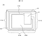
第1の実施形態になるRFIDタグ70は、タグ本体60と直立保持部50とで構成されている。タグ本体60は、基材5の上に導電材料、例えば金属板又は金属箔等により形成された平面状の微小ループアンテナ71と、この微小ループアンテナに一対の電極31a、31bを介して接続されたICチップ30とで構成されている。微小ループアンテナ71の内側には、アンテナ平面に直交する方向に開口し、ICチップ30と微小ループアンテナ間のインピーダンスの整合機能を有するスリット形状整合回路20が形成されている。ICチップ30は、整流部やマイクロプロセッサを含む集積回路を備えている。スリット形状整合回路20は、基材、例えばラミネートフィルムに開口を設けたものである。このように、本実施形態では、微小ループアンテナ71が、整合回路20を兼ねた整合回路兼用の微小ループアンテナとなっている。
交信周波数の波長をλとしたとき、微小ループアンテナ71のループ径又はループ長さ(長辺)は、λ/10程度以下、あるいはループ面積がλ2/100以下とするのが望ましい。微小ループアンテナは、きわめて薄く、例えば20μm程度の厚みであり、基材5によりタグ本体60の機械的な強度を確保している。
直立保持部50は、このような薄膜のアンテナ平面(ループ面)が金属面8に実質的に垂直になるようにして微小ループアンテナ71を金属面8に設置することで、整合回路20を高周波的に短絡しないようにする機能を有している。なお、直立保持部50は、微小ループアンテナ71と同じ材料からなる平坦な座面51(51A,51B,51C)を有し、たとえば矩形状の微小ループアンテナ71としたときの4つの辺のうちICチップ30の搭載されている辺を除く残りの3つの辺いずれかに直交するようにして3か所形成されている。ただし、必ずしもこれら3つの辺の全てに設ける必要はなく、少なくとも1か所形成されていればよい。また、図1では、取り付け角AGが90度すなわち、微小ループアンテナのループ面が取り付ける金属面8に垂直に立つようになっているが、若干傾斜していてもよい。すなわち、直立保持部50の座面51が微小ループアンテナ71となす角度AGは、後で述べるように、90度±30度の範囲(略直角)であればよい。
なお、微小ループアンテナ71の材料は、金属に限定されるものではなく、カーボンなどの非金属材料からなる導体、あるいは半導体でも良い。また、RFIDタグ70のスリット形状は、タグ本体60と直立保持部50とがL字形に組み合わされた形状に限定されるものではない。例えば、スリット形状がT字形であっても良く、あるいは全体の外形が直方体状であっても良く、ICチップ30と微小ループアンテナ71とのインピーダンス整合回路の役割を果たす形状であればさらに好都合である。
As a first embodiment of the present invention, the structure and operation of an RFID tag will be described. The RFID tag of the present embodiment is suitable for an application in which the RFID tag is installed and operated on a conductor surface or a metal surface (hereinafter referred to as a metal surface or a metal object).
FIG. 1 is a perspective view showing an example in which the RFID tag according to the first embodiment of the present invention is installed on a metal object.
The
When the wavelength of the communication frequency is lambda, the loop diameter or loop length of the small loop antenna 71 (long side) is, lambda / 10 or less, or desirably loop area and lambda 2/100 or less. The micro loop antenna is extremely thin, for example, about 20 μm thick, and the mechanical strength of the
The
The material of the
次に、本発明の第1の実施形態になるRFIDタグ70を、RFIDのインレット6を用いて製造する例を、図2(図2A、図2B)を用いて説明する。
図2Aは、本発明の実施形態のRFIDタグ70を制作するのに好適なダイポールアンテナ1からなるRFIDインレット6を説明する図である。RFIDインレット6は、基材5の上にアルミニウムなどの金属板又は金属箔により厚さが例えば10μm〜20μm程度のダイポールアンテナ1を形成したものである。図2Aには、ICチップ30が接続される電極31A、31b及びスリット状整合回路20の位置関係が示されている。略1/2波長のRFIDインレット6から破線で示した整合回路領域4を切り出す。
次に、図2Bに示したように、整合回路領域4で切り出したRFIDインレット6を破線B−Bで示す位置において、取り付け金属面8に電気的に接触させる場合は導電材料の面が外側に位置するようにして、取り付け金属面8に絶縁性の基材を介して電磁的に接する場合は導電材料の面が内側に位置するようにして、各々略直角に折り曲げ、タグ本体60と、このタグ本体60を垂直に保持する直立保持部50とを設ける。タグ本体60は金属面8に取り付け角AGが略直角のとき、換言すると微小ループアンテナ71の取り付け角AGが略直角のとき、金属対応のRFIDタグ70として機能する。すなわち、タグ本体60を垂直に保持することで、金属面8に設置された場合に、整合回路20を高周波的に短絡しないで済むようにする。換言すると、座部51の表面は微小ループアンテナと同じ導電材料の面であり、座部51を絶縁用の部材で構成する必要は無い。
直立保持部50は、タグ本体60の取り付け角AGが略直角であれば金属面8に接触して取り付けられてもかまわない。
Next, an example in which the
FIG. 2A is a diagram illustrating the
Next, as shown in FIG. 2B, when the
The
次に、本発明の第1の実施形態におけるRFIDタグ60のスリット状整合回路20について、図3(図3A、図3B)で説明する。このスリット状整合回路20の形状は様々あり、たとえば、図3Aに示したような、RFIDインレット6における“T”字形のスリット形状整合回路20Tを、切り出し線611で切断すると、“T”字形のスリット形状の整合回路を有するタグ本体60ができる。
また、図3Bに示したような、RFIDインレット6における“L”字形をしたスリット形状整合回路20Lの部分を、切り出し線611で切断すると、“L”字形をしたスリット形状の整合回路を有するタグ本体60ができる。
Next, the
Further, when the portion of the slit-shaped
このようにして、それぞれRFIDインレット6から整合回路領域4を切り出してタグ本体60を形成すると共に、この整合回路領域の下部を金属面に直立しやすくする直立保持部50に加工することで、図4(4A、4B)に示したようなRFIDタグ70が得られる。図4Aの例は“T”字形スリット形状整合回路20Tを有し、図4Bの例は、L”字形スリット形状整合回路20Lを有している。
In this manner, the
本実施例のRFIDタグ70は、“L”字又は“T”字などの形状をした整合回路が微小ループアンテナ71と兼用して(整合回路兼用の微小ループアンテナが)設けられており、RFIDインレット6のスリットがつくるループ面を、取り付ける金属面上に略90度で直立するように設置する。
In the
図5(図5A、図5B)は、巻き数が1回の微小ループアンテナ71を備えた本実施例のRFIDタグ70の作用、効果を説明する図である。図5Aは、巻き数が1回の微小ループアンテナ付きのRFIDタグ70を、金属面に設置したときのイメージRFIDタグ70Mの関係、すなわち、実像と虚像の足し算の説明図である。金属面8の上に置かれるRFIDタグ70とこれが投影してできるイメージRFIDタグ70Mでは、それぞれに流れる高周波電流iが境界面で打ち消す方向に、金属面8の垂直部分で同方向に流れる。
図5Bは、ループ巻き数が1回の場合の図5AのRFIDタグ70のループ面積は、金属面8を境界とする部分で高周波電流iが打ち消してできる2倍のループ面積、すなわちループ面A1とイメージループ面AMの合計面積を持つ微小ループアンテナ等価回路71Eと等価であることを示している。
FIG. 5 (FIG. 5A, FIG. 5B) is a figure explaining the effect | action and effect of the
FIG. 5B shows that the loop area of the
図6(図6A、図6B)は、巻き数が2回の微小ループアンテナ72を備えた本実施例のRFIDタグ70の作用、効果を説明する図である。図6Aは、2回巻き微小ループアンテナ72の場合において、金属面8の上に置かれるRFIDタグ70とこれが投影してできるイメージRFIDタグ70Mの関係を示し、それぞれに流れる高周波電流iが境界面で打ち消す方向に、金属面8の垂直部分で同方向に流れることを示している。
図6Bは、ループ巻き数が2回の場合のRFIDタグ70のループ面積は、金属面8を境界とする部分で高周波電流iが打ち消してできる2倍のループ面積、すなわちループ面A1とAMの合計面積をもつ2回巻き微小ループアンテナの等価回路72Eと等価であることを説明している。
このように、本実施例のRFIDタグ70は、RFIDタグを金属面に略垂直に立てることから、金属面上のRFIDタグ内の微小ループアンテナを流れる高周波電流と、金属面下に投影してできるイメージの微小ループアンテナに流れる高周波電流が、金属面の境界で平行な部分ではイメージのため、互いに反対向きに流れ打ち消し合い、垂直部分では互いに同方向に流れる。そのため、等価的に2倍のループ面積の微小ループアンテナとなり、自由空間および非金属面におかれる微小ループアンテナの感度より向上させることができる。
FIG. 6 (FIGS. 6A and 6B) is a diagram for explaining the operation and effect of the
FIG. 6B shows that the loop area of the
As described above, since the
図6の例は、巻き数が2回の場合を示しているが1.5でも3でもいくつであっても良い。図6ではあえて2回巻きで代表としている。一般には、周波数が高くなるほど巻き数を減少させて高周波損失を減らしている。UHFやマイクロ波では巻き数が1回程度である。 The example of FIG. 6 shows a case where the number of windings is two, but it may be 1.5, 3, or any number. In FIG. 6, it is representatively represented by two windings. In general, the higher the frequency, the lower the number of turns to reduce the high frequency loss. In UHF and microwaves, the number of turns is about once.
ここで、微小ループアンテナからの放射電力をP、交信電磁波の波長をλ、微小ループアンテナの巻き数をN、微小ループアンテナの面積をA、ループに流れる高周波電流をi、円周率をπとすると、下記非特許文献2「解説 アンテナの基礎」P.42から、
P = {20・(2π/λ)4・(N・A)2}・i2 (W)
で示される。
Pは巻き数Nと面積Aの積の2乗に比例することがわかる。
従って、N=1のとき、Aが2倍になるとPは4倍となり、1回巻きの微小ループアンテナの感度を、自由空間や非導体面に置かれるよりは導体面や金属面に置いた時そのイメージ反射を用いて格段に向上させるという効果がある。
非特許文献2 「解説 アンテナの基礎」、著者 岩井 陸路、発行所 東京電気大学出版局、 昭和42年11月25日初版
Here, the radiation power from the micro loop antenna is P, the wavelength of the communication electromagnetic wave is λ, the number of turns of the micro loop antenna is N, the area of the micro loop antenna is A, the high frequency current flowing through the loop is i, the circularity is π Then,
P = {20 · (2π / λ) 4 · (N · A) 2 } · i 2 (W)
Indicated by
It can be seen that P is proportional to the square of the product of the number of turns N and area A.
Therefore, when N = 1, when A is doubled, P is quadrupled, and the sensitivity of the one-turn micro-loop antenna is placed on the conductor surface or metal surface rather than on free space or non-conductor surface. At the same time, the image reflection can be used to greatly improve.
前記4倍の感度効果の検証として、微小ループアンテナを有するRFIDインレットを用いたサンプルタグを用意する。
インレットは日立製作所製のRKT102型とし、これを基材としての厚さ4mmの発泡スチロール材に、短辺5mmで長辺10mmの長方形ループに1回巻く。このとき、ICチップ部を長辺側10mmの中央部に配置する。これにより、短い辺が交信周波数の波長の略1/20波長、長い辺が1/10波長となる微小ループアンテナを備えた検証用のサンプルタグタグを実現している。
リーダはセコニック社製R001M型とし、これで飛距離測定を行う。
検証は金属板として1辺が200mmの正方形で厚み0.5mmのアルミ板中央にサンプルタグを設置した時の飛距離が、非金属板として1辺が200mmの正方形で厚み8mmのゴム板中央にサンプルタグを置いた時の飛距離の何倍か、を求めることで行う。
まず、サンプルタグをアルミ板に置いた時の飛距離、22mmを得た。
次いで、サンプルタグをゴム板に置いた時の飛距離、6mmを得た。(測定例1)
従って、飛距離比は約3.7倍となり、理論値4倍に近い数値を得ている。
測定に当たっては、サンプルタグが直線偏波、リーダが円偏波であるもののタグ近傍では、サンプルタグの設置方向により大きな感度差が生ずる。そこで、サンプルタグの向きを水平偏波と垂直偏波の中間である45度の方向に設置する。
ここでは説明しやすくするため、水平あるいは垂直偏波設置をリーダのアンテナ面の縦辺を垂直偏波、横辺を水平偏波として定義した。
As a verification of the fourfold sensitivity effect, a sample tag using an RFID inlet having a minute loop antenna is prepared.
The inlet is an RKT102 type manufactured by Hitachi, Ltd., which is wound once on a foamed polystyrene material having a thickness of 4 mm as a base material and a rectangular loop having a short side of 5 mm and a long side of 10 mm. At this time, the IC chip part is arranged at the central part of the
The reader is R001M manufactured by Seconic Co., Ltd., which performs flight distance measurement.
The verification is that the distance when a sample tag is placed in the center of an aluminum plate with a square of 200 mm on one side and a thickness of 0.5 mm as a metal plate is the center of a rubber plate with a square of 200 mm on one side and a thickness of 8 mm as a non-metal plate. This is done by finding the multiple of the flight distance when the sample tag is placed.
First, a flight distance of 22 mm was obtained when the sample tag was placed on an aluminum plate.
Next, a flying distance of 6 mm when the sample tag was placed on the rubber plate was obtained. (Measurement Example 1)
Therefore, the flight distance ratio is about 3.7 times, and a value close to the theoretical value of 4 times is obtained.
In measurement, although the sample tag is linearly polarized and the reader is circularly polarized, there is a large sensitivity difference in the vicinity of the tag depending on the installation direction of the sample tag. Therefore, the sample tag is installed in the direction of 45 degrees, which is intermediate between the horizontal polarization and the vertical polarization.
For ease of explanation, horizontal or vertical polarization is defined as vertical polarization on the reader antenna surface and horizontal polarization on the horizontal side.
また、微小ループアンテナのループ面が金属面に対して90度の角度のとき最大の飛距離になることを確認している。
確認方法として、まず、サンプルタグは上記測定例1の場合と同じRFIDインレットを使用し、これを基材としての寸法が幅2mmの厚みで1辺が10mmの正方形の発砲スチロール材の4つの10mm辺に沿う、正方形ループになるように1回巻いて、サンプルタグを作る。
次いで、このサンプルタグを測定例1の場合と同じ金属板およびリーダを使用し、金属板にループ面の交差角度別の飛距離測定を行う。偏波面はリーダの感度が高い方で飛距離測定する(測定例2)。
サンプルタグとの角度0のとき、これは平置きのときに相当するが、このときタグは応答せず、すなわち金属対応のタグとして動作しないことを確認し、サンプルタグとの角度30または150度のとき飛距離は10mm、サンプルタグとの角度60または120度のとき同30mm、サンプルタグとの角度90度のとき同40mm、これは金属面に直立でこのとき最大の飛距離になることを確認している。
It has also been confirmed that the maximum flight distance is obtained when the loop surface of the micro loop antenna is at an angle of 90 degrees with respect to the metal surface.
As a confirmation method, first, the sample tag uses the same RFID inlet as in the above-mentioned measurement example 1, and this is used as a base material with dimensions of 2 mm in width and 10 mm on one side of 10 mm square foamed polystyrene material. Make a sample tag by winding it once in a square loop along the side.
Next, the same metal plate and reader as those in Measurement Example 1 are used for this sample tag, and the flight distance is measured on the metal plate for each intersection angle of the loop surface. The polarization plane is measured for the flight distance when the reader sensitivity is higher (measurement example 2).
When the angle with the sample tag is 0, this corresponds to the case of flat placement. At this time, the tag does not respond, that is, it is confirmed that the tag does not operate as a metal-compatible tag. The distance is 10mm, 30mm when the angle with the sample tag is 60 or 120 degrees, and 40mm when the angle with the sample tag is 90 degrees. This means that the distance is upright on the metal surface. I have confirmed.
上記測定結果をまとめたもの、すなわち、取り付け角AGと飛距離の関係を、図7に示す。図7から、ピーク感度の8割が90度を中心とした±30度の範囲にはいっていることが分かる。すなわち、直立保持部50の座面51が微小ループアンテナ71となす角度AGは、90度±30度の範囲(略直角)とするのが望ましい。
さらに、測定例1で用いた発砲スチロール材の代わりに、ゴム磁石によるサンプルタグ厚み3mm、幅4mm、長さ6mmに代えた小型の微小ループアンテナを構成し、金属対応のRFIDタグが実現できることを確認している。長さをさらに短縮した3mm長の場合であっても通常のリーダ/ライタであり、例えばセコニック社製R001M型リーダで交信可能な金属対応のRFIDタグが実現できることを確認している。同サンプルタグで厚み0.4mm幅4mm長さが10mm程度においても動作することを確認している(測定例3)。
これらは、前記放射電力を表す式からループ面の形状には依存しないで面積が0でない限り放射がなされるという示唆と一致する。
FIG. 7 shows a summary of the measurement results, that is, the relationship between the mounting angle AG and the flight distance. From FIG. 7, it can be seen that 80% of the peak sensitivity is in the range of ± 30 degrees centering on 90 degrees. That is, it is desirable that the angle AG formed by the
Furthermore, instead of the foamed polystyrene material used in Measurement Example 1, a small micro-loop antenna is used instead of a rubber magnet sample tag with a thickness of 3 mm, width of 4 mm, and length of 6 mm, and a metal-compatible RFID tag can be realized. I have confirmed. Even when the length is further reduced to 3 mm, it is confirmed that a normal RFID reader / writer can be realized, and, for example, a metal-compatible RFID tag that can be communicated with an R001M reader manufactured by Seconic Corporation can be realized. It has been confirmed that the sample tag operates even when the thickness is 0.4 mm, the width is 4 mm, and the length is about 10 mm (measurement example 3).
These agree with the suggestion that radiation is performed as long as the area is not zero, without depending on the shape of the loop surface, from the formula representing the radiated power.
本実施例のRFIDタグは、取り付け金属面と、直接結合又は接着材等で間接的に電磁結合させて使用することができる。
図8(図8A、図8B)は、本実施例のRFIDタグ70を金属面8に直接、それぞれ横長にあるいは縦長に取り付けた事例の説明図である。
本実施例のRFIDタグを、例えば図8に示したように直接結合により、取り付け金属面8と電気的に接続または、絶縁体を介し間接結合により金属面8と容量的に電磁結合させることにより、取り付けたRFIDタグ70の直上又は直上から離れた場所から交信することができる。
The RFID tag of this embodiment can be used by being electromagnetically coupled directly to the mounting metal surface with a direct coupling or an adhesive.
FIG. 8 (FIG. 8A, FIG. 8B) is explanatory drawing of the example which attached the
For example, the RFID tag of this embodiment is electrically connected to the mounting
すなわち、図9に示したように、金属面8に取り付けたRFIDタグ70から、高周波電流iが金属面8の上に進行波WFが左右に流れてゆき、端部で発生する反射波WRと進行波WFとが干渉し、1/2波長ごとにうねる半波長周期WLの干渉波Wが生ずる。
図9では、金属面8が1/2波長の整数倍で明瞭な節部WVと腹部WPができることを示しているが、1/2波長以上の任意の長さのときは節部WVおよび腹部WPが不明瞭となる干渉波Wになる。このときは空中への電磁放射も減少する。このような任意の長さの干渉波Wの状況は図示していない。
このように、RFIDタグを金属面と電磁結合させると、金属面に高周波電流が流れ、高周波電流は交信周波数の波長を周期とした進行波となり金属面を伝播し、伝播方向にある不連続部で戻る反射波と干渉する波のうねりである波高の高い腹部と波高の低い節部をもち、腹部と腹部あるいは節部と節部の間隔が半波長の整数倍の周期となる干渉波や腹部と節部の明瞭な定在波から電磁波を放射させ、取り付けたRFIDタグの直上又は直上から離れた場所から交信可能となる。
本発明によれば、きわめて薄い整合回路兼用の微小ループアンテナのループ面を直立保持部で略直立して保持するようにしてRFIDタグを構成したので、金属物上に設置可能な極めて小型のRFIDタグを提供できる。すなわち、本発明によれば、交信電磁波の波長をλとした時、λ/4からICチップサイズ、例えば0.3mm以下の寸法のRFIDタグを実現できる。
That is, as shown in FIG. 9, a high-frequency current i flows from the
FIG. 9 shows that the
As described above, when the RFID tag is electromagnetically coupled to the metal surface, a high-frequency current flows through the metal surface, and the high-frequency current becomes a traveling wave having a period of the communication frequency as a period, propagates through the metal surface, and is a discontinuous portion in the propagation direction. Interfering waves and abdomen, which have a high-abdominal abdomen and a low-wave node, which are swells of the waves that interfere with the reflected wave returning at, and the interval between the abdomen and abdomen or between the node and the node is a period that is an integral multiple of a half wavelength Electromagnetic waves are radiated from a clear standing wave at the node, and communication is possible from a location directly above or away from the top of the attached RFID tag.
According to the present invention, since the RFID tag is configured such that the loop surface of the very thin matching loop also used as a matching circuit is held substantially upright by the upright holding portion, the extremely small RFID that can be installed on a metal object Can provide tags. That is, according to the present invention, when the wavelength of the communication electromagnetic wave is λ, an RFID tag having a size of λ / 4 to an IC chip size, for example, 0.3 mm or less can be realized.
次に、本発明の第2の実施形態について、説明する。本発明のRFIDタグの形状および製造方法は、実施例1に示した構成、方法に限定されるものではない。本実施形態では、RFIDタグ70の製法として、微小ループアンテナと兼用の整合回路をICチップ上に集積し、半導体で一体化したことを特徴とする。
すなわち、図10に示したように、全て半導体で金属対応のタグを形成できることもできる。この場合、微小ループアンテナパターン71Sと整合回路20Sとが兼用となる。
すなわち、IDなどのIC論理回路31のパターンと直接接続した同一の半導体基材上に、半導体製造プロセスにより微小ループアンテナ兼整合回路のパターン等が形成された略直方体状のRFIDタグ本体60と、前記ICチップ上のループ面が取り付け金属面8に略垂直に立つように前記RFIDタグ本体の表面に形成された直立支持部50としての側面、すなわち直立座部51(図では3面、51A,51B,51C)を形成した半導体チップレベルのRFIDタグ70とすることができる。本実施例によれば、交信電磁波の波長をλとした時、λ/4からICチップサイズの寸法のRFIDタグを実現できる。なお、直立支持部50は、例えば、半導体基板すなわち基材5の厚みを厚くすることで、直立座部として必要な面積および機械的強度を確保することができる。
Next, a second embodiment of the present invention will be described. The shape and manufacturing method of the RFID tag of the present invention are not limited to the configuration and method shown in the first embodiment. In the present embodiment, the manufacturing method of the
That is, as shown in FIG. 10, a metal-compatible tag can be formed using a semiconductor. In this case, the minute loop antenna pattern 71S and the matching circuit 20S are combined.
That is, a substantially rectangular parallelepiped RFID tag
本実施例によれば、半導体製造プロセスのみで、金属物上に設置可能な小型のRFIDを提供できる。
本実施例のRFIDタグも、整合回路20Sが微小ループアンテナ71Sと兼用されている。このRFIDタグ70をそのループ面が取り付ける金属面上に90度で直立するようにして設置すると、金属面下に投影したイメージのループ面、すなわち前記微小ループアンテナにイメージの高周波電流が流れるが、金属面の境界で平行な部分では互いに打ち消し合うように流れ、金属面上と金属面下に垂直な部分では互いに同方向に流れ、等価的に自由空間の2倍のループ面積の微小ループアンテナとなる。
According to this embodiment, it is possible to provide a small RFID that can be installed on a metal object only by a semiconductor manufacturing process.
In the RFID tag of this embodiment, the matching circuit 20S is also used as the minute loop antenna 71S. When this
次に、本発明の第3の実施形態として、金属面に取り付けし易くしたRFIDタグ70について、図11で説明する。
本実施形態では、RFIDタグ70を、外部からの衝撃や圧力に対してICチップや整合回路を保護する為に、または取り付けの利便性を向上する為に、高周波で損失の少ない丈夫な誘電体や磁性体、あるいはそれらの混合材の樹脂、セラミックや絶縁性接着剤等で被い取り扱いや取り付けをしやすくかつ機械的に強化したものである。本実施形態でも、RFIDタグ70は、取り付け金属面と、直接結合又は接着材等で間接的に電磁結合させて使用することができる。
すなわち、図11に示したように、RFIDタグ70を誘電体又は磁性体製充填材70Cで被って丈夫にし、かつ、ネジなどの止め具70Bで金属面8に取り付けしやすくしたRFIDタグ70である。この場合、止め具は金属製のネジであってもよく絶縁性の樹脂であってもよい。金属ネジの場合は、高周波電流iを引き込む誘導性または容量性ポストとしての作用を期待できることがあるので長さや位置を調節すると感度を改善できる。
Next, as a third embodiment of the present invention, an
In the present embodiment, the
That is, as shown in FIG. 11, the
図12の例では、金属面8の段差部などに接着剤70Dなどを用いてRFIDタグ70を簡単に取り付けられる。高周波電流iが段差部の表面を流れ、経路途中にあるRFIDタグ70のICチップ30を通り動作させる。
In the example of FIG. 12, the
図13の例は、金属の窪地81やネジ穴などへ埋設する取り付け方法を示している。すなわち、タグ本体60を埋設し、接着剤70D等で固定し金属面8の表面から突出しない取り付けが可能である。
このように、本発明によるRFIDタグは、小型のため金属板の段差部、窪地、コーナ部又は、ネジ頭など凸部の影など丈夫な物陰に退避して接着剤程度で取り付けることができるので特段の保護金具を省略、あるいは取り付け用の凹部切削作業などの省略ができる利点があり取り付け作業負担の軽減となる。
The example of FIG. 13 shows a mounting method embedded in a
As described above, since the RFID tag according to the present invention is small in size, it can be attached to the step of a metal plate by a strong object such as a stepped portion, a depression, a corner portion, or a shadow of a convex portion such as a screw head. There is an advantage that a special protective metal fitting can be omitted or a concave cutting operation for mounting can be omitted, and the mounting work burden can be reduced.
次に、本発明の第4の実施形態として、RFIDタグの保護金具により微小ループアンテナの機械的強度を向上させた、RFIDタグ70について説明する。なお、本実施形態では、RFIDタグ本体60の微小ループアンテナに関し、ループ面を金属の取り付け面に略直立して保持する。
本実施形態で微小ループアンテナを形成する方法としては、実施例1、2で述べたように、RFIDインレット6の整合回路20の領域を切り出して、取付け金属面8に略直立させるものが挙げられる。この場合、整合回路のスリットは微小ループアンテナの機能を受け持ち2つの機能を兼用する役目を担う。微小ループアンテナを形成する他の方法は、前記整合回路20を切り出す代わりに、RFIDインレットをICチップを含む所定の長さに切り、これを少なくとも1回巻いて新たに微小ループアンテナを作り、これを取付け金属面8に略直立させるものである。このRFIDインレットから新たに微小ループアンテナを作る方法については、後で詳細に説明する。いずれの手段で形成される場合でも、微小ループアンテナは単独では機械的強度が十分とはいえないので、以下に述べるように、この微小ループアンテナを内部に保持する方式を採用するのが望ましい。
Next, as a fourth embodiment of the present invention, an
As a method for forming a micro loop antenna in the present embodiment, as described in the first and second embodiments, the region of the matching
本実施例のRFIDタグは、外部からの静電気やサージ電流などの電気的衝撃に対し、ICチップを保護する目的で貝構造、折返し構造あるいは折り返し端子構造等シールド構造の金具の内側に配置し、少なくともICチップ30や整合回路20が短絡しない様に絶縁役のスペーサを介して電磁結合させた保護金具により電気的衝撃に対してシールドしたものである。スペーサ61Sは空気であっても、誘電体または磁性体の充填剤70Cであってもよい。通常はスペーサ61Sと充填剤70Cとを、誘電体または磁性体からなる同一の材料で一体的に構成するのが好適である。
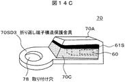
第4の実施形態において、RFIDタグ70の保護金具の形状は、図14Aの貝構造保護金具70SD1、図14Bの折り返し構造保護金具70SD2、図14Cの折り返し端子構造保護金具70SD3、図14Dの端子構造保護金具70SD4のような例があり、各々、機械的強度を向上させることができる。なお、各図において、スペーサ61Sは、誘電体や磁性体などで形成されたタグ本体60の整合回路が保護金具と短絡するのを阻止するための隔離材である。
The RFID tag of this embodiment is arranged inside a metal fitting of a shield structure such as a shell structure, a folded structure, or a folded terminal structure for the purpose of protecting the IC chip against an external electric shock such as static electricity or surge current, At least the
In the fourth embodiment, the shape of the protective fitting of the
図14Eは、RFIDタグ70の保護金具70Aを、微小ループアンテナと一体に形成したRFIDタグ70の構造の説明図である。この例は、UHFやマイクロ波帯の周波数が使用される用途に適したRFIDタグである。図14Eの(a)は斜視図、(b)はICチップ30の近くを拡大した図であり、ここにはスリット状整合回路20が金属面8に平行に配置される。(c)は(a)の縦断面図である。
まず、この例のRFIDタグ70のスリット形状整合回路20は、取付ける金属面8又はスペーサ61Sを介して保護金具70Aに平行なため、微小ループアンテナの機能を持つことが出来ない。そこで、ICチップ30を含む帯状のRFIDインレット6を少なくとも1回巻いて微小ループアンテナ71として機能するようにし、この微小ループアンテナ71のループ面の一部、すなわち、ICチップ30の配置される側とは反対側のループの縁(側辺)を座部又は取付け面51とすることにより、取付ける金属面8に略直立するように構成されている。70Cは誘電体または磁性体充填材である。この例のRFIDタグ70は、帯状RFIDインレット6を、例えばUHFやマイクロ波帯のダイポールアンテナを基調としたRFIDインレットでIC部30を含む所定の長さにカットし、このカットされたインレットを、充填剤70Cを芯材にして微小ループアンテナ71の寸法にまるめて、1回巻きのループを形成したものである。
この例では、RFIDタグ70の微小ループアンテナが保護金具(アーム)70Aと一体に形成される。例えば、RFIDインレット6として、図2Aに示したような、ICチップ30が接続される電極31a、31b及びスリット状整合回路20を備えたものを用いる。ただ、図2Aの整合回路兼用の微小ループアンテナとは異なり、RFIDインレット6の両端を切り出さずにそのまま折り曲げて1回巻きのループ状の微小ループアンテナ71を形成する。この場合、取付ける金属面8に対して、整合回路20は略平行であり、微小ループアンテナ71は略直立するようになっている。整合回路20は、“L”字又は“T”字などの形状をしたスリット状となっている。すなわち、帯状のRFIDインレット6を、微小ループアンテナ71の寸法にICチップ30が含まれるようにして、1回巻きにし、さらに保護金具を一体に形成する。このとき、微小ループアンテナ71の1つのループの1回巻き分に相当する始点と終点がつながる接続地点領域72Cでは、直接接続又は間接接続の電磁結合のいずれかで接続する。さらに、電波放射方向にあるループ上のIC部30の上側に、スペーサ部分61Sを介するなど絶縁しながら、RFIDインレットを接続地点72Cからさらに半回巻き連続して延長した保護金具すなわちアーム70A付きのRFIDタグとする。例えば、RFIDインレット6の一端をさらに連続略半巻き程延長することで、タグ本体60を覆うアーム70Aを形成し、RFIDタグ70とする。この例のRFIDタグ70では、ループの1回巻き分における微小ループアンテナ71の金属面8と平行な部分の長さをλ/10程度、あるいは1回巻き分のループの内側の面積をλ2/100以下とするのが望ましい。一方、ループサイズの下限値は、このループに含まれるICチップ30のサイズに応じて決まる。アーム70Aの長さは、λ/4まで延長しても良い。アーム70Aを設けることで、RFIDタグ70に静電気やサージ電流に耐力(静電遮蔽)を持たせ、感度を高めることが出来る。さらに、アーム70Aを丈夫な金属製材料とすることで、機械的強度も同時に向上させることが出来る。
FIG. 14E is an explanatory diagram of a structure of the
First, since the slit
In this example, the minute loop antenna of the
図14Fは、保護金具を備えた他の例になるRFIDタグ70の構造説明図である。この例のRFIDタグ70は、図14Eの例と同様に、帯状のRFIDインレット6を少なくとも1回巻いて微小ループアンテナとして機能するように巻いたループ面が、取付け金属面8に略直立するように構成されている。図14Eの例ではアーム70Aがタグ本体60と一連の帯状RFIDインレットで構成されているのに対して、図14Fの例は、微小ループアンテナ71を備えたタグ本体60の部分、すなわちループ巻き数の1回部分を、保護金具すなわちアーム70Aとは分離し独立させた構造となっている。図14Fの(a)は斜視図、(b)は(a)のタグ本体60の拡大図、(c)は(a)の縦断面図である。金属製アーム70Aは折り返し構造保護金具70SD2として機能する。タグ本体60を挟んで折り返し構造保護金具70SD2の金属製アーム70Aとは反対の側を座部又は取付け面51とすることにより、ループ面が取付け金属面8に略直立するように構成されている。この例でも、RFIDタグ70に静電気やサージ電流に耐力を持たせ(静電遮蔽)、感度を高めることが出来るだけでなく、アーム70Aを丈夫な金属製材料とすることで、機械的強度も同時に向上させることが出来る。
この例のRFIDタグ70において、タグ本体60は前記非特許文献2で示される放射電力と巻き数Nと微小ループアンテナの面積Aの関係式、及び後述の図16A,図16Bから明らかなように、本発明の中で説明しているスリット形状の整合回路を切り出して導いた微小ループアンテナと見立てたタグ本体60に相当する。従って、図5Bで説明した等価回路と同じになり、図1等の例に対して電磁波的には区別が出来ない等価物とみなせる。従って、図14E、図14Fの例についても、図14A〜図14Dに示した貝構造保護金具70SD1、折り返し構造保護金具70SD2、折り返し端子構造保護金具70SD3、端子構造保護金具70SD4など各種保護金具に内装したときと同等の動作が可能であり、同等の効果が得られる。以下、に述べる各実施例に関しても、図14E、図14Fに示した帯状の微小ループアンテナを採用することで、同等の効果が得られる。
FIG. 14F is an explanatory diagram of a structure of an
In the
図15により、第4の実施形態の作用、効果を説明する。第4の実施形態の各例では、保護金具がサージ電流・溶接電流・静電気放電電流Iなどを金属面8に放電することで電気的衝撃からタグ本体60内部のICチップ30を保護する。図15は、RFIDタグ70SD2を、折り返し構造保護金具により保護した例である。
このように、本実施例のRFIDタグは、外部からの静電気やサージ電流などの電気的衝撃に対し、ICチップを保護する目的で貝構造、折返し構造あるいは折り返し端子構造等シールド構造の金具の内側に配置し、少なくとも整合回路が短絡しない様にスペーサを介して電磁結合させる保護金具で電気的衝撃に対してシールドしたRFIDタグを実現できるだけでなく、保護金具にネジ穴を設け脱落防止に役立つ。
また、静電気の高電圧やサージ電流の大電流に対しする耐力検証として、圧電素子による着火器具の発する高電圧を直接、シールド構造で保護された折り返し端子構造のRFIDタグに空中放電し、正常動作していることを確認している。
また、大電流として電気溶接機によりシールド構造で保護された折り返し端子構造のRFIDタグに100A程度の電流で溶接しても正常動作していることを確認している。
The operation and effect of the fourth embodiment will be described with reference to FIG. In each example of the fourth embodiment, the protective metal fittings protect the
As described above, the RFID tag according to the present embodiment is used to protect the IC chip from external electric shocks such as static electricity and surge current, and to protect the inside of the metal shell having a shield structure such as a shell structure, a folded structure, or a folded terminal structure. In addition to realizing an RFID tag that is shielded against electrical shock by a protective metal fitting that is electromagnetically coupled through a spacer so that at least the matching circuit is not short-circuited, a screw hole is provided in the protective metal fitting to help prevent falling off.
In addition, as a strength verification against high static electricity voltage and surge current, high voltage generated by igniting equipment with piezoelectric elements is directly discharged in the air to the RFID tag with folded terminal structure protected by shield structure. I have confirmed that.
Further, it has been confirmed that even when welding with an electric current of about 100 A to an RFID tag having a folded terminal structure protected by a shield structure with an electric welding machine as a large current, it is confirmed that the device is operating normally.
また、本実施形態の他の例として、RFIDタグの保護金具は、保護されるRFIDタグの微小ループアンテナのアンテナ導体が幅をもつことで実質的微小ループアンテナ面積はアンテナ導体部分を除いたループ面積となるが、保護金具が微小ループアンテナの外部にあることから外側から大回りに高周波磁束をループに誘導する事で、実質の微小ループアンテナ面積を保護金具が囲う位置まで拡大し感度を向上させ、かつ、貝構造、折返し構造あるいは折り返し端子構造等シールド構造が、機械的強度の向上並びに電気的衝撃に対する耐力を向上させている。
すなわち、図16(図16A、図16B)の例では、保護金具により実質的な微小ループアンテナ71の面積を拡大し感度を改善している。
まず、図16Aは保護金具付きのRFIDタグの斜視図、図16Aの保護金具部分の断面S−S’を図16Bの(b)に示し、保護金具が無いタグ本体60だけの場合の断面を図16Bの(a)に示している。それぞれの微小ループアンテナ71の外部にあることから大回りに高周波の磁束がループに誘導される様子を説明している。ここで、図16Bの(a)は保護金具無し高周波磁束Φ1に保護金具無しループ面縦寸法A0が対応している。これを図16Bの(b)の保護金具70SD2で保護すると、大回りの保護金具有り高周波磁束Φ2となり、結果的に保護金具により拡大ループ面縦寸法ASとなるため、実質的な微小ループアンテナ71の面積を拡大し感度を改善していることを説明している。
このように、本実施例の金属対応RFIDタグは、保護されるRFIDタグの微小ループアンテナのアンテナ導体が幅をもつことで実質的微小ループアンテナ面積はアンテナ導体部分を除いたループ面積となるが、保護金具が微小ループアンテナの外部にあることから外側から大回りに高周波磁束をループと等価であるスリットに誘導する事で、実質の微小ループアンテナ面積を保護金具が囲う位置まで拡大し感度向上させ、かつ、貝構造、折返し構造あるいは折り返し端子構造等シールド構造が、機械的強度の向上並びに電気的衝撃に対する耐力を向上させるRFIDタグを実現できる。
As another example of the present embodiment, the RFID tag protective metal fitting has a width of the antenna conductor of the minute loop antenna of the RFID tag to be protected, so that the substantial minute loop antenna area is a loop excluding the antenna conductor portion. However, since the protective bracket is outside the micro loop antenna, high frequency magnetic flux is guided to the loop from the outside to increase the actual micro loop antenna area to the position where the protective bracket surrounds and improve the sensitivity. In addition, a shield structure such as a shell structure, a folded structure, or a folded terminal structure improves mechanical strength and resistance to electrical shock.
That is, in the example of FIG. 16 (FIG. 16A, FIG. 16B), the area of the
First, FIG. 16A is a perspective view of an RFID tag with a protective metal fitting, and a cross section SS ′ of the protective metal fitting portion of FIG. 16A is shown in FIG. 16B (b). This is shown in (a) of FIG. 16B. A state in which high-frequency magnetic fluxes are induced in the loops around because they are outside the respective
Thus, in the metal-compatible RFID tag of this embodiment, the antenna conductor of the minute loop antenna of the RFID tag to be protected has a width, so that the substantial minute loop antenna area becomes the loop area excluding the antenna conductor portion. Because the protective bracket is outside the micro loop antenna, high frequency magnetic flux is guided from outside to the slit that is equivalent to the loop, so that the actual micro loop antenna area is expanded to the position where the protective bracket surrounds and the sensitivity is improved. In addition, a shield structure such as a shell structure, a folded structure, or a folded terminal structure can realize an RFID tag that improves mechanical strength and resistance to electrical shock.
また、また、本実施形態の他の例として、モノポールアンテナ長の金具で感度を向上させた事例を、図17(図17A、図17B、図17C、図17D、図17E、図17F、図17G)で説明する。これらの例では、保護金具を交信電磁波の媒質中の1/4波長の長さのモノポールアンテナ長の寸法で保護金具を構成し共振を積極的に助長させ、非金属面上でも金属面上でも交信可能になるよう感度を向上させている。
すなわち、図17の各例は、シールド構造の金具、すなわち図17Aが貝構造の保護金具70SD1、図17Bが折り返し構造保護金具70SD2、図17Cが折り返し端子構造70SD3、図17Dが端子構造保護金具70SD4を、各々、媒質中のモノポールアンテナ長大凡λg/4の金具とし、感度を向上させたRFIDタグ70の事例である。金具には例えばステンレス鋼を用いる。
As another example of the present embodiment, an example in which the sensitivity is improved by a metal pole with a monopole antenna length is shown in FIG. 17 (FIGS. 17A, 17B, 17C, 17D, 17E, 17F, FIG. 17G). In these examples, the protective bracket is configured with a 1 / 4-wavelength monopole antenna length in the electromagnetic wave medium to actively promote resonance, and even on a non-metal surface or on a metal surface. However, the sensitivity is improved so that communication is possible.
That is, in each example of FIG. 17, a shield structure metal fitting, that is, FIG. 17A is a shell structure protection metal fitting 70SD1, FIG. 17B is a folded structure protection metal fitting 70SD2, FIG. 17C is a folded terminal structure 70SD3, and FIG. Is a case of the
さらに、図17Eの例は、図14Eの微小ループアンテナ71の金属製アーム70Aを接続地点領域72CからさらにE=λg/4 あるいはそれに近い長さ(大凡λg/4)だけ水平方向に連続して延長しICチップ30を上から覆う、アーム70A付きの形状となっている。タグ本体60を挟んで金属製アーム70Aとは反対の側を座部又は取付け面51とすることにより、ループ面が取付け金属面8に略直立するように構成されている。
また、図17Fの例は、図14Fの微小ループアンテナ71の上下の金属製アーム70Aを接続地点領域72CからさらにE=λg/4 あるいはそれに近い長さ(大凡λg/4)だけ水平方向に連続して延長しICチップ30を覆う、アーム70A付きの貝構造の保護金具70SD1となっている。
また、図17Gの例は、表面模様がC型平面保護金具70SD5を備えたRFIDタグ70を示している。図17Gにおいて、(a)はRFIDタグ70の斜視図、(b)は(a)のa−a’断面図である。図17Bの例が凸形の突起部を持つのに対し、図17Gの例では、金具70SD5に取り付け穴78と、主に媒質中のモノポールアンテナ長で共振させる構造の金属製アーム70Aを同一平面に形成し、突起部を平滑化した構造のRFIDタグ70となっている。金属製アーム70Aはλg/4 あるいはそれに近い長さ(大凡λg/4)だけ水平方向に連続して延長しICチップ30を上から覆っている。金属製アーム70Aの周囲にはC字模様またはU字形の隙間79がある。アーム70Aの直下(最適な位置はアームの付け根位置とは限らず整合をとると根本から少しずれることがある)に、タグ本体60がスペーサ61Sを介して内装され、ICチップ30が保護金具の内側に配置されている。この例では、タグ本体60は図14Fの(c)に示したような断面構成となっている。
さらに図17Gの例において、金具70SD5の全長を半波長に共振する長さにした場合、自由空間又は非金属上においてもより高い感度が実現できる。
Further, in the example of FIG. 17E, the
Further, in the example of FIG. 17F, the upper and
Moreover, the example of FIG. 17G has shown the
Furthermore, in the example of FIG. 17G, when the entire length of the metal fitting 70SD5 is set to a length that resonates at a half wavelength, higher sensitivity can be realized even in free space or on a non-metal.
このように、RFIDタグ70の感度を向上させるべく、貝構造、折返し構造あるいは折り返し端子構造等シールド構造に代表される保護金具の他、交信電磁波の媒質中の1/4波長の長さのモノポールアンテナ長の寸法で保護金具を構成し、共振を積極的に助長させ、非金属面上でも金属面上でも交信可能になるよう感度を向上させたRFIDタグを実現できる。
In this way, in order to improve the sensitivity of the
本発明のRFIDタグ70は、金属面上のみならず非金属面上に設置しても高い感度で交信可能とすることもできる。例えば、タグ本体60を、交信電磁波の1/2波長に共振する長さの金属板中央に窪地など掘り込んでダイポールアンテナの給電点に配置するように設置したり、例えば1/4波長の長さのモノポールアンテナ長の寸法の保護金具2個を接続してできる略半波長の長さのアンテナの給電点にタグ本体60を配置したりしてできるダイポールアンテナサイズの保護金具を構成することにより、共振を積極的に助長させて非金属面上でも金属面上でも高い感度で交信可能とするRFIDタグを実現できる。
図18Aの例は、保護金具の寸法を半波長に共振するダイポールアンテナ長λ/2で構成し感度を向上させたRFIDタグ70の事例を示す図である。
The
The example of FIG. 18A is a diagram illustrating an example of an
図18Bの例は、H形平面保護金具70SD6を備えたRFIDタグ70の例である。図18Bの(a)はRFIDタグ70の斜視図、(b)は(a)のa−a’断面図である。図17Gの例における金属製アーム70Aが1つであるのに対し、図18Bの例では、2つの金属製アーム70Aを対向させ、隙間79を設けて両アームの先端を接触させないで配置した構造を持つ。すなわちダイポールアンテナ金具77の表面に隙間79による“H”字形の模様ができる。どちらか一方のアーム70Aの直下(最適な位置は電磁波モードのアームの整合をとるべく中央から少しずらして決める)に、タグ本体60がスペーサ61Sを介して内装され、ICチップ30が保護金具の内側に配置される。その為、タグ本体60が電気的機械的に強化された構造となる。さらに金具70SD6の全長が半波長の寸法であるため、自由空間を含めた非金属面上でも、金属面上に取り付けた場合においても、高い感度で交信できるRFIDタグ70を実現できる。
The example of FIG. 18B is an example of the
図18Cの例は、一対の電磁波モード発生兼用保護金具70SD7を用いたRFIDタグ70である。図18Cの(a)は斜視図、(b)は(a)のa−a’断面図である。この例では、2枚の略円形の金属板(電磁波モード発生兼用保護金具)70SD7がその略中央(最適な位置は電磁波モードの整合をとるべく中央から少しずらして決める)に、スペーサ61Sを介してタグ本体60を挟み、誘電体または磁性体充填材70Cで固定している。このRFIDタグ70を取り付け金属面8に設置し、上方から交信すると、上面の金属板70SD7の外部表面および内側表面にマイクロ波理論から知れる高周波電流が流れ、電磁波モードとしては、円形共振板のTM基本モードの電流iTMが分布する。この電流の最良の共振条件は、70C内部における波長すなわち媒質中の波長をλg、円周率をπ、金属板の外形寸法をDiとすると、
Di=(1.841/π)λg
で与えられる。ここで、1.841は、微分形の第一種ベッセル関数の最小の根の有効数値4桁である。
この例では、TM基本モードで共振する高周波電流がタグ本体60とスペーサ61Sを介して電磁結合し、電磁波モード発生兼用保護金具70SD7と一体化したRFIDタグ70として機能する。
図18Cの(a)では、高周波電流分布の交互に入れ替わる一瞬の状態を止めて矢印表記している。ちなみに矢印の始点が+の最大電位部分で矢印の行き先終点が−の最大電位部分、矢印の中央が0電位(図中の0電位線)になり、ここは同時に電流が最大値になる。0電位部分は小さな取り付け穴78やネジを貫通しても共振状態に与える影響が少ない。
図18Cの例の試作を通して、金属板の平面形状が円形であっても正方形であっても、RFIDタグを構成したとき、高々1波長程度の飛距離感度では形状の差と感度の差異を見出しにくいことを確認した。1つの試作例としては、金属板を1辺が16mmの略正方形で置換し、充填樹脂を比誘電率20の材料とし、周波数を2.45GHz、タグ本体60は日立製作所製のミューチップインレット(RKT102)から形成した。この試作RFIDタグを、0電位部分に直径が3mmのネジ2つを通して十分広い金属面に設置した場合、セコニック社製リーダR001Mで飛距離を測定して約100mmの飛距離を得た。さらに、他の試作例として、金属円板を直径71.5mmでねじ止めなし、充填物を比誘電率1の空気とし、前述の例と同じタグ本体、前述の例と同じリーダR001Mで飛距離を測定し、180mmの飛距離を得た。このように発明者は試作例により、TM基本モードの共振と0電位の影響を確認している。
The example of FIG. 18C is an
Di = (1.841 / π) λg
Given in. Here, 1.841 is an effective numerical value of 4 digits of the minimum root of the differential type first-order Bessel function.
In this example, the high frequency current resonating in the TM basic mode is electromagnetically coupled via the tag
In (a) of FIG. 18C, an instantaneous state where the high-frequency current distribution is alternately switched is stopped and indicated by an arrow. Incidentally, the starting point of the arrow is the maximum potential portion of +, the destination end point of the arrow is the maximum potential portion of −, the center of the arrow is 0 potential (the 0 potential line in the figure), and at this time, the current becomes the maximum value simultaneously. The zero potential portion has little influence on the resonance state even if it passes through the small mounting
Through the trial manufacture of the example of FIG. 18C, even when the planar shape of the metal plate is circular or square, when the RFID tag is configured, a difference in shape and a difference in sensitivity are found with a flight distance sensitivity of about one wavelength at most. It was confirmed that it was difficult. As one prototype example, the metal plate is replaced with a square having a side of 16 mm, the filling resin is made of a material having a relative dielectric constant of 20, the frequency is 2.45 GHz, and the
なお、図18Cの例では、2枚の略円形の金属板(同図では金属板が電磁波モード発生兼用保護金具70SD7としている)を用いているが、図18Dの例に示すように、取り付け金属面側は取り付けた時金属面が重複するので、下側の金属板はこれを省略し、1枚の電磁波モード発生兼用保護金具70SD8のみとしても良い。さらに、図18Dに示すように、自由空間において半波長で共振しやすくするため、“H”字形となるように2つのアーム70Aの先端が接触しないように対向させ、一方のアーム直下(電磁波モードの整合をとると、最適な位置はアーム直下のいずれかの地点)にタグ本体60を、スペーサ61Sを介して誘電体または磁性体充填材70Cあるいは接着剤70Dによって固定しても良い。すなわち、図18Dの例は、半波長共振/電磁波モード発生兼用保護金具70SD8とタグ本体60とを一体化したRFIDタグ70である。
この例のタグの特徴は、全体の厚みを金属板1枚分だけ薄くすることができるだけでなく、金属面以外の、たとえば自由空間においても動作が可能になることである。さら、図18Cの例同様に、0電位線上に取り付け穴78やネジなど設けることが可能である。これは、金属板が1枚のため取り付け金属面におかれる時TM基本モードの電流iTMが分布するが、自由空間ではTM基本モードの共振が困難となる代わりに、金属板外形寸法Diが半波長共振寸法に近いため、概ね半波長共振電流IDが最大電流ではないが、実用的十分な感度のRFIDタグ70として機能する。
TM基本モードの金属板外形寸法Diは、交信波長を122mm、媒質を空気、円周率をπ、とすると、 Di=(1.841/π)・122から71.5mm となる。一方、空気中の一般的な半波長共振寸法は、122/2から61mmである。すなわち、これら(金属板外形寸法Diと一般的な半波長共振寸法)の差異は、17%である。
高々1波長程度の飛距離感度では、Diを最初からこれらの中間の寸法(この場合の中間値は66mm 差異9%)とし、金属面から非金属面まで安定した感度の、しかも薄型の適用範囲の広いRFIDタグ70の実現が可能である。
In the example of FIG. 18C, two substantially circular metal plates (in FIG. 18C, the metal plate is the electromagnetic wave mode generating / protecting metal fitting 70SD7) are used. However, as shown in the example of FIG. Since the metal surface overlaps when the surface is attached, the lower metal plate may be omitted and only one electromagnetic wave mode generating / protecting metal fitting 70SD8 may be provided. Further, as shown in FIG. 18D, in order to easily resonate at a half wavelength in a free space, the two
The feature of the tag of this example is not only that the entire thickness can be reduced by one metal plate, but also that the operation is possible in a free space other than the metal surface, for example. Further, as in the example of FIG. 18C, it is possible to provide a mounting
The metal plate outer dimension Di of the TM basic mode is Di = (1.841 / π) · 122 to 71.5 mm where the communication wavelength is 122 mm, the medium is air, and the circumference is π. On the other hand, typical half-wave resonance dimensions in air are 122/2 to 61 mm. That is, the difference between these (the metal plate outer dimension Di and the general half-wave resonance dimension) is 17%.
For distance sensitivity of about one wavelength at most, Di is set to an intermediate dimension between them (in this case, the intermediate value is 66 mm, 9% difference), and it has a stable sensitivity from a metal surface to a non-metal surface, and a thin application range. A
また、ダイポールアンテナ金具77を採用することで、感度が向上する一方、寸法が約2倍の長さになる。
図19は、感度向上のため、例えばモノポールアンテナ75の金具を2個背中合わせに連結したような構造で、全長が空気中の半波長の寸法を有するとしたダイポールアンテナ金具77を形成でき、感度がダイポールアンテナ並みに向上する一方、寸法は約2倍の長さになる。
Further, by adopting the
FIG. 19 shows a structure in which, for example, two
すなわち、感度を優先した場合、寸法が大きくなるが、本実施例によると、交信電磁波の1/2波長に共振する長さの金属板中央に窪地など掘り込んでダイポールアンテナの給電点に配置するように設置したり、1/4波長の長さのモノポールアンテナ長の寸法の保護金具2個を折り返し接続部分で背中合わせに接続してできる略半波長の長さのアンテナの給電点にRFIDタグを配置したりしてできるダイポールアンテナサイズの保護金具を構成し、共振を積極的に助長させて非金属面上でも金属面上でも交信可能となるように感度を向上させたRFIDタグを実現できる。 That is, when sensitivity is given priority, the size increases, but according to the present embodiment, a hollow is dug in the center of the metal plate having a length that resonates with a half wavelength of the communication electromagnetic wave, and is arranged at the feeding point of the dipole antenna. RFID tag at the feeding point of an antenna with a length of about half-wavelength, which can be installed by connecting two protective brackets of the length of a monopole antenna with a length of 1/4 wavelength back to back at the connection part A dipole antenna-sized protective metal fitting can be constructed by arranging the antenna, and it is possible to realize an RFID tag with improved sensitivity so that resonance can be actively promoted to enable communication on a non-metal surface or a metal surface. .
次に、本発明の第5の実施形態として、本発明のRFIDタグを、離れた箇所から交信するのに使用する例について図20(図20A、図20B)で説明する。
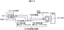
本実施形態では、上記いずれかの実施例のRFIDタグを、交信電磁波の波長に比べ長い針金状の金属棒表面にRFIDタグの長手方向が針金に平行、RFIDタグ内部のスリット面が針金表面に略直立する様に設置し(図20A)、あるいは金属棒の端部にRFIDタグを延長する様に直結又は電磁結合で接続し(図20B)金属棒表面に高周波電流を流し、高周波電流は交信周波数の波長を周期とした進行波となり金属面を伝播し、伝播方向にある不連続部で戻る反射波と干渉する波のうねりである波高の高い腹部と波高の低い節部をもち腹部と腹部あるいは節部と節部の間隔が半波長の整数倍の周期となる干渉波や腹部と節部の明瞭な定在波から電磁波を放射させ、取り付けたRFIDタグの直上又は直上から離れた場所において交信可能とした金属棒と一体化した形状のRFIDタグ及びその交信法を特徴とする。
図20Aに示したように、タグ本体60を針金状金属棒9の表面にタグ本体の長手方向が金属棒に平行になるように取り付け、針金状金属棒9の表面に高周波電流iの干渉波を生じさせ電磁波を放射することで、リーダ/ライタR/Wによりタグ本体60を取り付けた直上又は、直上から離れた箇所から交信できる。
Next, as a fifth embodiment of the present invention, an example in which the RFID tag of the present invention is used to communicate from a remote location will be described with reference to FIGS. 20 (FIGS. 20A and 20B).
In this embodiment, the RFID tag according to any one of the above-described examples is arranged such that the longitudinal direction of the RFID tag is parallel to the wire and the slit surface inside the RFID tag is on the surface of the wire. Installed so as to be almost upright (Fig. 20A), or connected to the end of the metal rod by direct connection or electromagnetic coupling so as to extend the RFID tag (Fig. 20B). Waves with a high wave height and nodes with low wave heights, which are wave swells that propagate through the metal surface and interfere with reflected waves that return at discontinuities in the propagation direction, and are traveling waves with a frequency of frequency as a period. Alternatively, in the place where the distance between the node part and the node part is an integer multiple of a half wavelength, or electromagnetic waves are radiated from the clear standing wave of the abdomen and the node part, and directly above or just above the attached RFID tag Communication Wherein the ability and the RFID tag and its communication method of a shape that is integrated with a metal rod.
As shown in FIG. 20A, the
また、図20Bに示したように、RFIDインレット6を針金状金属棒9の端部に取り付け、針金状金属棒9表面に高周波電流iの干渉波を生じさせ電磁波を放射することで、リーダ/ライタR/WによりRFIDインレット6を取り付けた直上又は、直上から離れた場箇所から交信できる。
なお、図20A,20Bにおいて感度を向上させるための取り付け位置は金属棒の端部から1/4波長の地点又は、ここを起点とした1/2波長周期の地点に設置するのが好適である。
Further, as shown in FIG. 20B, the
20A and 20B, it is preferable that the mounting position for improving the sensitivity is installed at a point of 1/4 wavelength from the end of the metal rod or a point of 1/2 wavelength period starting from this point. .
RFIDタグを取り付けた場所から離れた所で交信したい場合、RFIDタグを交信電磁波の波長に比べ長い針金状の金属棒表面にRFIDタグの長手方向が針金に平行、RFIDタグ内部のスリット面が針金に略直立する様に設置し、あるいは金属棒の端部にRFIDタグを延長する様に直結又は電磁結合で接続し金属棒表面に高周波電流を流し、高周波電流は交信周波数の波長を周期とした進行波となり金属面を伝播し、伝播方向にある不連続部で戻る反射波と干渉する波のうねりである波高の高い腹部と波高の低い節部をもち腹部と腹部あるいは節部と節部の間隔が半波長の整数倍の周期となる干渉波や腹部と節部の明瞭な定在波から電磁波を放射させ、取り付けたRFIDタグの直上又は直上から離れた場所において交信可能とした金属棒と一体化した形状のRFIDタグ及びその交信法を提供できる。 If you want to communicate at a place away from the place where the RFID tag is attached, the RFID tag has a wire-like metal rod surface that is longer than the wavelength of the electromagnetic wave to be communicated, and the longitudinal direction of the RFID tag is parallel to the wire, and the slit surface inside the RFID tag is the wire It is installed so that it is almost upright, or connected to the end of the metal rod by direct or electromagnetic coupling so that the RFID tag is extended, and a high frequency current flows through the surface of the metal rod. Waves that are traveling waves, propagate through the metal surface, interfere with reflected waves that return at discontinuities in the propagation direction, and have waved abdomen with high and low wave heights. Electromagnetic waves are radiated from interference waves whose intervals are an integral multiple of half the wavelength and clear standing waves of the abdomen and nodes, enabling communication at a location directly above or away from directly above the attached RFID tag. It can provide an RFID tag and a communication method of an integrated shape with Shokubo.
さらに、上記実施形態の金属棒を金属パイプに絶縁を介して非接触に内挿し、同軸ケーブル又は同軸管(自由に曲がる同軸ケーブルも以降同軸管と呼ぶ)内を伝播する波の一種である同軸モード波を発生させ、同軸管の両端部又は片端部の開口部で金属棒を1/10波長の微小ダイポールアンテナの寸法程度から1/4波長のモノポールアンテナの寸法程度に延ばし、同軸管の外部表面に高周波電流を流す。これにより、高周波電流は交信周波数の波長を周期とした進行波となり金属面を伝播し、伝播方向にある不連続部で戻る反射波と干渉する波のうねりである波高の高い腹部と波高の低い節部をもち腹部と腹部あるいは節部と節部の間隔が半波長の整数倍の周期となる干渉波や腹部と節部の明瞭な定在波を発生させ、同軸管の外部表面に伝播する干渉波や定在波からの電磁波放射により交信可能とする同軸管と一体化した同軸管形状のRFIDタグ及びその交信法を提供できる。 Furthermore, the metal rod of the above embodiment is inserted in a metal pipe in a non-contact manner through insulation, and is a type of wave that propagates in a coaxial cable or a coaxial pipe (a coaxial cable that is freely bent is also referred to as a coaxial pipe hereinafter). A mode wave is generated, and the metal rod is extended from the size of a 1/10 wavelength microdipole antenna to the size of a 1/4 wavelength monopole antenna at both ends or one end of the coaxial tube. A high frequency current is applied to the external surface. As a result, the high-frequency current becomes a traveling wave with the frequency of the communication frequency as a period, propagates through the metal surface, and undulates the wave that interferes with the reflected wave returning from the discontinuous part in the propagation direction. Interfering waves with a node and abdomen and abdomen or the interval between the node and the node being an integral multiple of half a wavelength and clear standing waves between the abdomen and the node are generated and propagated to the outer surface of the coaxial tube It is possible to provide a coaxial tube-shaped RFID tag integrated with a coaxial tube capable of communication by electromagnetic wave radiation from an interference wave or standing wave, and a communication method therefor.
さらに、図21(図21A、図21B)に示したように、同軸ケーブル又は同軸管Cの内部導体にタグ本体60を設置し、RFIDタグが、外部の導体表面の各所で交信できる。
図21Aは、同軸ケーブル又は同軸管Cの内部導体にタグ本体60を設置し、同軸内部導体に流れる高周波電流iを同軸端部に直結されたモノポールアンテナ又は微小ダイポールアンテナ76などのアンテナにより同軸内部及び外部の導体表面に高周波電流を流し、外部の導体表面のいたるところでリーダ/ライタR/Wと交信できることを示している。
図21Bは、同軸ケーブル又は同軸管Cの両端部にアンテナ部を設け内部と外部の導体に流れる高周波電流iを積極的に流れやすくしたことを示している。
なお、同軸内部の電磁界分布は遮断周波数のない同軸モード(TEM)が分布するが特に図示していない。
Furthermore, as shown in FIG. 21 (FIGS. 21A and 21B), the tag
In FIG. 21A, a tag
FIG. 21B shows that the antenna portions are provided at both ends of the coaxial cable or the coaxial tube C so that the high-frequency current i flowing through the internal and external conductors can be positively flowed.
Note that the electromagnetic field distribution inside the coaxial line is distributed in the coaxial mode (TEM) having no cutoff frequency, but is not particularly shown.
また、同軸ケーブル又は同軸管Cのアンテナ部C1は、円柱状、テーパ状、ループ状などいろいろな形状にすることができる。アンテナ部の寸法は、1/10波長程度の長さの微小ダイポールアンテナ76から1/4波長の長さのモノポールアンテナ長λ/4までの範囲で、同軸端部の両端に設置しても良く、片側でも良い。 Further, the antenna portion C1 of the coaxial cable or the coaxial tube C can have various shapes such as a columnar shape, a tapered shape, and a loop shape. The dimensions of the antenna section may range from a minute dipole antenna 76 having a length of about 1/10 wavelength to a monopole antenna length λ / 4 having a length of 1/4 wavelength. Good, one side is acceptable.
さらに、本実施例においては、上記実施形態の金属棒を金属パイプに絶縁を介して非接触に内挿し、同軸ケーブル又は同軸管(自由に曲がる同軸ケーブルも以降同軸管と呼ぶ)内を伝播する波の一種である同軸モード波を発生させ、同軸管の両端部又は片端部の開口部で金属棒を1/4波長のモノポールアンテナの寸法から微小ダイポールアンテナの寸法程度に延ばし、同軸管の外部表面に高周波電流を流すことができる。これにより、高周波電流は交信周波数の波長を周期とした進行波となり金属面を伝播し、伝播方向にある不連続部で戻る反射波と干渉する波のうねりである波高の高い腹部と波高の低い節部をもち腹部と腹部あるいは節部と節部の間隔が半波長の整数倍の周期となる干渉波や腹部と節部の明瞭な定在波を発生させ、同軸管の外部表面に伝播する干渉波や定在波からの電磁波放射により交信可能とする同軸管と一体化した同軸管形状のRFIDタグの実現及びその交信法を提供できる。 Furthermore, in this example, the metal rod of the above embodiment is inserted into a metal pipe in a non-contact manner through insulation, and propagates in a coaxial cable or a coaxial pipe (a coaxial cable that is freely bent is also referred to as a coaxial pipe hereinafter). A coaxial mode wave, which is a type of wave, is generated, and a metal rod is extended from the size of a monopole antenna of 1/4 wavelength to the size of a minute dipole antenna at the opening at both ends or one end of the coaxial tube. A high frequency current can flow through the external surface. As a result, the high-frequency current becomes a traveling wave with the frequency of the communication frequency as a period, propagates through the metal surface, and undulates the wave that interferes with the reflected wave returning from the discontinuous part in the propagation direction. Interfering waves with a node and abdomen and abdomen or the interval between the node and the node being an integral multiple of half a wavelength and clear standing waves between the abdomen and the node are generated and propagated to the outer surface of the coaxial tube It is possible to provide a coaxial tube-shaped RFID tag integrated with a coaxial tube capable of communication by electromagnetic wave radiation from an interference wave or standing wave, and a communication method thereof.
前記実施形態3から5におけるタグ本体60は、図1におけるタグ本体60と、図14Fにおけるタグ本体60とが、図5Bで説明する等価回路が同じになり、交換可能である。したがって、図示した例以外にも、形が異なるが電磁波的に同等なタグ本体の組み合わせが種々可能である。
さらに、前記実施形態3から5におけるタグ本体60は、図14Eの略半巻き延長した金属アーム70Aが無くなった場合のタグ本体と等価であり、図5Bで説明する等価回路が同じになり交換可能である。したがって、図示した例以外にも、形が異なるが電磁波的に同等なタグ本体の全ての組み合わせが種々可能である。
The
Furthermore, the tag
本発明の第6の実施形態として、図22(図22A、図22B)に示したように、金属面8の奥まった箇所にRFIDタグ70を設置し、アタッチ式検出器具Dと交信するようにして使用する事も出来る。
本実施形態では、リーダ/ライタのアンテナ面に外付けするダイポールアンテナを内蔵したアタッチ式検出器具であって、ダイポールアンテナが該リーダ/ライタのアンテナ面から平行に0ないし交信電磁波の略10波長程度で、好適は1/4波長の位置に取り付けられる器具を用いる。これにより、互いに密集している、あるいはリーダ/ライタを近づけることのできない狭い箇所に設置された、前記各実施例のRFIDタグへ、リーダ/ライタに取り付けた該器具のダイポールアンテナの中央部が高周波電流の最大領域であることから、この部分を目的のRFIDタグに電磁誘導範囲まで接近させて、1対1の交信を可能にする外付けアタッチ式検出器具およびその交信法を提供できる。
図22Aは、奥まった箇所に設置され、応答しにくいRFIDタグ70と交信する方法を説明する図である。リーダ/ライタR/Wに取り付けるアタッチ式検出器具Dはダイポールアンテナ棒D2と絶縁性の支持体D1で構成されている。アタッチ式検出器具Dがリーダ/ライタR/Wのアンテナ面DAからD2が、0ないしは1/2波長程度隔てた取り付け位置hに平行にセットされ、金属窪地81に設置されたタグ本体60の直近にダイポールアンテナ棒D2の中心部を近接させD2の特に中央部に誘起される高周波電流iとタグ本体60を共通に貫通する高周波磁束Φとの電磁誘導を活用した交信を行う。
As a sixth embodiment of the present invention, as shown in FIG. 22 (FIGS. 22A and 22B), an
In the present embodiment, an attachment type detection device incorporating a dipole antenna externally attached to the antenna surface of a reader / writer, the dipole antenna is parallel to the antenna surface of the reader / writer and is approximately 0 to about 10 wavelengths of communication electromagnetic waves. In this case, it is preferable to use an instrument that is attached to a quarter wavelength position. As a result, the central portion of the dipole antenna of the instrument attached to the reader / writer is connected to the RFID tag of each of the above-described embodiments installed in a narrow place where the reader / writer cannot be brought close to each other. Since this is the maximum current range, this portion can be brought close to the target RFID tag to the electromagnetic induction range, and an externally attached detection instrument that enables one-to-one communication and its communication method can be provided.
FIG. 22A is a diagram for explaining a method of communicating with an
また、本実施例によれば、リーダ/ライタのアンテナ面に外付けするダイポールアンテナを内蔵するアタッチ式検出器具であって、ダイポールアンテナが該リーダ/ライタのアンテナ面から平行に0ないし交信電磁波の略10波長程度で、好適には1/4波長の位置に取り付けられる器具とする。これにより、互いに密集している、あるいはリーダ/ライタを近づけることのできない狭い箇所に設置された前記各実施例のRFIDタグへ、リーダ/ライタに取り付けた該器具のダイポールアンテナの中央部が高周波電流の最大領域であることから、この部分を目的のRFIDタグに電磁誘導範囲まで接近させて、1対1の交信を可能にする外付け非接触のアタッチ式検出器具およびその交信法を提供できる。
また、図22Bは、密集したRFIDタグ70をアタッチ式検出器具Dのダイポールアンテナ棒D2の感度の高い中央部が目的のRFIDタグ70を指し示し、1対1に確実に交信する方法を示している。
Further, according to the present embodiment, there is provided an attachment type detection instrument incorporating a dipole antenna externally attached to the antenna surface of the reader / writer. The instrument is attached to a position of about a quarter wavelength, preferably a quarter wavelength. As a result, the central portion of the dipole antenna of the device attached to the reader / writer is connected to the RFID tag of each of the embodiments described above in a narrow place where the reader / writer cannot be brought close to each other. Therefore, it is possible to provide an external non-contact attached detection instrument and its communication method that allows one-to-one communication by bringing this portion close to the electromagnetic induction range.
Further, FIG. 22B shows a method of reliably communicating one-to-one with the dense RFID tags 70 in which the high-sensitivity central portion of the dipole antenna rod D2 of the attached detection device D points to the
この交信方法によると、交信電磁波の波長に比べて広い、例えば縦200mm横200mmのアルミ板上に外形寸法が厚み3mm幅4mm長さ6mmである小型のRFIDタグを間隙が1mm程度で平行に密集させた場合、直径2mm長さ52mmの該ダイポールアンテナ棒の中央部をRFIDタグに近接し1対1の識別ができることを確認している。
なおRFIDタグは日立製作所製のインレット(RKT102)、リーダはセコニック社のR001Mを使用している。
According to this communication method, small RFID tags whose outer dimensions are 3 mm wide, 4 mm long and 6 mm long on an aluminum plate that is wider than the wavelength of the communication electromagnetic wave, for example 200 mm long and 200 mm wide, are closely packed in parallel with a gap of about 1 mm. In this case, it has been confirmed that the central portion of the dipole antenna rod having a diameter of 2 mm and a length of 52 mm is close to the RFID tag and can be identified one-to-one.
The RFID tag uses an inlet (RKT102) manufactured by Hitachi, Ltd., and the reader uses R001M manufactured by Seconic.
本発明の第7の実施形態として、本発明のRFIDタグ、あるいは一般のRFIDタグが、電磁波を反射吸収する障害物を通して設置され交信電磁波が直接届かない場合における、障害物を通して検出する検出器具とその交信法について、図23から図26で説明する。
本実施例の対象となる交信電磁波の障害物GNDとして、コンクリート、アスファルト、土砂、水、海水、金属物等があり、RFIDタグがこれらを通して設置されているものとする。本実施例では、延長検出器具DTRにより交信する。延長検出器具は、RFIDタグと直接交信する検出部DTと、この信号を伝送する伝送部と、リーダ/ライタ側に近接する再放射部TRと、これを接続する伝送部Tとで構成されている。検出部はRFIDタグと直接交信する役割を有し、微小ループ、モノポール、ダイポールまたはセラミックアンテナ等いずれかの種類の1つのアンテナで構成する。伝送部は交信する電磁波を他端に届ける役割を有し、同軸線、平衡線、ストリップ線、導波管、誘電体棒等いずれかの種類の1つのアンテナで構成する。再放射部は、これにアタッチするリーダ/ライタと電磁結合する役割を有し、微小ループ、モノポール、ダイポール、セラミック、パッチアンテナまたは電磁ホーン等いずれかの種類の1つのアンテナで構成可能である。最良の組み合わせは、交信電磁波によって異なるが、交信電磁波をLF/HF帯とすれば、検出部と再放射部は微小ループアンテナが好適である。UHF/マイクロ波帯の場合は、検出部が微小ループ、モノポール、ダイポール、セラミック等のアンテナから選択し、再放射部はダイポール、セラミック、パッチアンテナ等のアンテナが好適となり、伝送部はいずれの電磁波帯域でも同軸線が好適である。
As a seventh embodiment of the present invention, there is provided a detection instrument for detecting through an obstacle when the RFID tag of the present invention or a general RFID tag is installed through an obstacle that reflects and absorbs electromagnetic waves and the communication electromagnetic wave does not reach directly. The communication method will be described with reference to FIGS.
It is assumed that there are concrete, asphalt, earth and sand, water, seawater, metal objects, and the like as obstacles GND for electromagnetic waves to be communicated in this embodiment, and RFID tags are installed therethrough. In this embodiment, communication is performed using the extension detection device DTR. The extension detection instrument includes a detection unit DT that directly communicates with the RFID tag, a transmission unit that transmits this signal, a re-radiation unit TR that is close to the reader / writer side, and a transmission unit T that connects the detection unit DT. Yes. The detection unit has a role of directly communicating with the RFID tag, and is configured by one type of antenna such as a micro loop, a monopole, a dipole, or a ceramic antenna. The transmission unit has a role of delivering electromagnetic waves to be communicated to the other end, and is configured by one type of antenna such as a coaxial line, a balanced line, a strip line, a waveguide, or a dielectric rod. The re-radiating part has a role of electromagnetic coupling with a reader / writer attached to the re-radiating part, and can be configured by one type of antenna such as a micro loop, a monopole, a dipole, a ceramic, a patch antenna, or an electromagnetic horn. . The best combination differs depending on the communication electromagnetic wave, but if the communication electromagnetic wave is in the LF / HF band, the detection unit and the re-radiation unit are preferably micro loop antennas. In the case of UHF / microwave band, the detection unit is selected from antennas such as micro loops, monopoles, dipoles, ceramics, etc., and the re-radiation unit is preferably an antenna such as dipoles, ceramics, patch antennas, etc. A coaxial line is also suitable in the electromagnetic wave band.
図23の例は、LF/HF帯の場合の、最良の延長検出器具DTRの構成図である。検出部DTLが微小ループアンテナで形成され、さらに感度を向上させるために同調コンデンサTCCで共振を調節しても良い。再放射部TRLを、微小ループアンテナで形成されリーダ/ライタR/Wと交信できる位置に近接させ、さらに感度を向上させるため同調コンデンサTCCで共振をとっても良い。伝送部TCXは同軸線としている。なお、DTLおよびTRLは、それぞれの近接する微小ループアンテナ径を概ね同じような寸法と巻き線数にすると、交信感度を向上させやすい。
図24の例は、UHF/マイクロ波帯の場合の延長検出器具DTRであり、検出部DTCがセラミックアンテナで形成されている。交信対象のRFIDタグ70が狭い所にある場合に有効である。再放射部TRDは、ダイポールアンテナで代表される線状のアンテナで形成され、リーダ/ライタR/Wと交信できる位置に近接させる。DTCとTRDをつなぐ伝送部TCXは同軸線としている。
図25の例は、図24の例における検出部DTCを、再放射部TRDのダイポールアンテナと同じ構造の検出部DTDとしたものである。DTDとTRDをつなぐ伝送部TCXは同軸線としている。この例は、金属平面レベルに埋設されたRFIDタグ70と交信するとき、十分な交信感度が得られる特徴がある。
図26の例は、図24の例における検出部DTCを1/4波長の長さのモノポールアンテナテナとした検出部DTMを備えており、このDTMとTRDをつなぐ伝送部TCXを同軸線としている。この例は、金属管の内壁面や底部に取り付けられたRFIDタグ70を、管の開口部から検出部DTMを挿入して交信することができる。
このように、本実施例の延長式のRFIDタグ検出器具は、交信電磁波がLF/HF帯の場合、前記検出部と前記再放射部を微小ループアンテナ、前記伝送部は同軸線とする。また、交信電磁波がUHF/マイクロ波帯の場合は、前記検出部に微小ループ、モノポール、ダイポール、セラミック等のいずれか1つのアンテナを選択し、前記再放射部はダイポール、セラミック、パッチアンテナ等のいずれか種類の1つのアンテナを選択し、前記伝送部は同軸線として一体的に構成する。
The example of FIG. 23 is a configuration diagram of the best extension detection instrument DTR in the case of the LF / HF band. The detection unit DTL may be formed of a minute loop antenna, and resonance may be adjusted by a tuning capacitor TCC in order to further improve sensitivity. The re-radiating part TRL may be made close to a position formed by a minute loop antenna and capable of communicating with the reader / writer R / W, and resonance may be taken with a tuning capacitor TCC in order to further improve sensitivity. The transmission unit TCX is a coaxial line. Note that DTL and TRL can easily improve communication sensitivity when the diameters of adjacent micro loop antennas are approximately the same size and number of windings.
The example of FIG. 24 is an extension detection instrument DTR in the case of the UHF / microwave band, and the detection unit DTC is formed of a ceramic antenna. This is effective when the
In the example of FIG. 25, the detection unit DTC in the example of FIG. 24 is a detection unit DTD having the same structure as the dipole antenna of the re-radiating unit TRD. The transmission part TCX connecting DTD and TRD is a coaxial line. This example is characterized in that sufficient communication sensitivity can be obtained when communicating with the
The example of FIG. 26 includes a detection unit DTM in which the detection unit DTC in the example of FIG. 24 is a monopole antenna tener having a length of ¼ wavelength, and the transmission unit TCX connecting this DTM and TRD is used as a coaxial line. Yes. In this example, the
As described above, in the extension type RFID tag detection instrument of the present embodiment, when the communication electromagnetic wave is in the LF / HF band, the detection unit and the re-radiation unit are micro loop antennas, and the transmission unit is a coaxial line. In addition, when the communication electromagnetic wave is in the UHF / microwave band, any one antenna such as a micro loop, a monopole, a dipole, and a ceramic is selected for the detection unit, and the re-radiation unit is a dipole, a ceramic, a patch antenna, etc. Any one type of antenna is selected, and the transmission unit is integrally configured as a coaxial line.
図23から図26の例に示した延長検出器具のその他の活用として、通常のRFIDタグおよび本発明による十分小型化されたタグ本体60が、手の届きにくい、あるいは交信電磁波の届きにくい個所にある場合にも応用できる。たとえば、天井、壁面、路面、マンホール下部そのほか危険区域など近づくことに労力がかかる場合、既存のリーダ/ライタのアンテナ部に非接触にアタッチする本実施例の延長検出器具を用いることで、作業負担を軽減する遠隔交信活用が可能となる。
発明者は、図23から図26の例において、伝送部Tを同軸線(1.5D2V)としその長さがいずれも5m程度で、十分に動作することを確認している。なお、確認時に用いたリーダは、HF帯で大成ラミック社製マルチリーダモジュールSTL920B、マイクロ波ではセコニック社製ハンディーリーダR001Mである。
As another application of the extension detection device shown in the examples of FIGS. 23 to 26, a normal RFID tag and a sufficiently small tag
The inventors have confirmed that in the examples of FIGS. 23 to 26, the transmission unit T is a coaxial line (1.5D2V) and the length thereof is about 5 m, and the operation is sufficiently performed. The reader used at the time of confirmation is a multi-reader module STL920B manufactured by Taisei Lamic in the HF band, and a handy reader R001M manufactured by Seconic in the microwave.
1 : ダイポールアンテナ
20 : スリット形状整合回路
20L : “L”字形スリット形状整合回路
20S : 半導体チップ上整合回路
20T : “T”字形スリット形状整合回路
30 : ICチップ
31 : IC論理回路
31A : 電極
31B : 電極
4 : 整合回路領域(整合回路の領域を切り出した部分)
5 : 基材
50 : 直立保持部
51 : 座部又は取付け面
51A : 座部又は取付け面
51B : 座部又は取付け面
51C : 座部又は取付け面
6 : RFIDインレット
60 : タグ本体
611 : 切り出し線
61S : スペーサ
70 : RFIDタグ
70A : 金属製アーム
70B : 止め具
70C : 誘電体又は磁性体充填材
70D : 接着剤
70M : イメージRFIDタグ
70SD1 : 貝構造保護金具
70SD2 : 折り返し構造保護金具
70SD3 : 折り返端子構造保護金具
70SD4 : 端子構造保護金具
70SD5 : C形平面保護金具
70SD6 : H形平面保護金具
70SD7 : 電磁波モード発生兼用保護金具
70SD8 : 半波長共振/電磁波モード発生兼用保護金具
71 : 微小ループアンテナ
71E : 微小ループアンテナ等価回路
71S : 微小ループアンテナパターン
72 : 2回巻き微小ループアンテナ
72C : ループの始点と終点の接続地点領域
72E : 2回巻き微小ループアンテナ等価回路
75 : モノポールアンテナ
76 : 微小ダイポールアンテナ
77 : ダイポールアンテナ
78 : 取り付け穴
79 : 隙間
8 : 金属面
81 : 金属面窪地
9 : 針金状金属棒
R/WA : リーダ/ライタ内部のアンテナ
GND : 交信電磁波の障害物
DTR : 延長検出器具
DT : 検出部
DTL : 検出部の微小ループアンテナ
DTM : 検出部のモノポールアンテナ
DTD : 検出部のダイポールアンテナ
DTS : 検出部のセラミックアンテナ
T : 伝送部
TCX : 同軸線
TR : 再放射部
TRL : 再放射部の微小ループアンテナ
TCC : 同調コンデンサ
TRD : 再放射部のダイポールアンテナ
AG : 取り付け角
I : サージ電流・溶接電流・静電気放電電流
Q : 静電気
i : 高周波電流
iTM : TM基本モード電流
ID : 半波長共振電流
Di : 外形寸法
A1 : ループ面
AM : イメージループ面
AS : 拡大面縦寸法
A0 : 保護金具無しループ面縦寸法
W : 干渉波
WF : 進行波
WR : 反射波
WP : 腹部
WV : 節部
WL : 半波長周期
Φ : 高周波磁束
Φ1 : 保護金具無し高周波磁束
Φ2 : 保護金具有り高周波磁束
λg : 媒質中の波長
λg/4 : 媒質中のモノポールアンテナ長
λ/4 : モノポールアンテナ長
λ/2 : ダイポールアンテナ長
R/W : リーダ/ライタ
C : 同軸ケーブル又は同軸管
C1 : 同軸ケーブル又は同軸管のアンテナ
D : アタッチ式検出器具
D1 : 支持体
D2 : ダイポールアンテナ棒
DA : リーダ/ライタのアンテナ面
h : 取り付け位置
B-B : 折り曲げ線
a−a’ :断面
S−S’ : 断面。
1: Dipole antenna 20: Slit-shaped
5: Base material 50: Upright holding portion 51: Seat or mounting
R / WA: Reader / writer internal antenna
GND : Obstacle of communication electromagnetic wave
DTR: Extension detection device
DT: Detector
DTL: Micro loop antenna of the detector
DTM: Monopole antenna for detector
DTD: Dipole antenna of the detector
DTS: Ceramic antenna of the detector
T: Transmission section
TCX: Coaxial line
TR: Re-radiation part
TRL: Micro loop antenna for re-radiating part
TCC: Tuning capacitor
TRD: Dipole antenna AG for re-radiating part: Mounting angle
I: Surge current, welding current, electrostatic discharge current
Q: Static electricity
i: High frequency current
iTM: TM fundamental mode current ID: Half-wave resonance current
Di: External dimensions
A1: Loop surface
AM: Image loop surface
AS: Vertical dimension of enlarged surface
A0: Vertical dimension of loop surface without protective bracket
W: Interference wave
WF: Traveling wave
WR: Reflected wave
WP: Abdomen
WV: Node
WL: Half-wave period Φ: High-frequency magnetic flux Φ1: High-frequency magnetic flux Φ2 without protective metal fittings: High-frequency magnetic flux λg with protective metal parts λg: Wavelength λg / 4 in the medium: Monopole antenna length λ / 4 in the medium: Monopole antenna length λ / 2: Dipole antenna length
R / W: Reader / Writer
C: Coaxial cable or coaxial pipe
C1: Coaxial cable or coaxial tube antenna
D: Attached detection instrument
D1: Support
D2: Dipole antenna rod
DA: Reader / writer antenna surface
h: Mounting position
BB: Folding line
a−a ′: Cross section
S−S ′: Cross section.
Claims (10)
絶縁層を介して前記ICチップを覆う金属製アームと、
前記微小ループアンテナのループ面が取り付け金属面に実質的に垂直になるようにして前記RFIDタグ本体を金属部材に取り付けるための取り付け面とを備え、
前記微小ループアンテナは、電磁波放射方向にある前記ICチップを含む少なくとも1回巻きのループとして形成されており、
前記金属製アームと前記微小ループアンテナとは、1つの前記ループの1回巻き分に相当する始点と終点がつながる接続地点領域において、機械的に接触し電気的にも導通される接続構造、若しくは、機械的に分離しつつ電気的には電磁結合により接続される接続構造の何れかの接続構造を有しており、
前記金属製アームは、前記ICチップ及び前記微小ループアンテナを挟んで前記取り付け面よりも電磁波放射方向の側において、前記ループの終点から該ループの巻き方向に沿って一方向に延びており、少なくとも前記ループの略半巻きに相当する長さだけ前記ICチップを覆っており、
前記RFIDタグ本体の交信周波数の波長をλとしたとき、前記金属製アームの長さが前記ICチップのサイズ乃至λ/4であることを特徴とするRFIDタグ。 An RFID tag body including an IC chip and a micro loop antenna electrically connected to the IC chip;
A metal arm that covers the IC chip via an insulating layer;
An attachment surface for attaching the RFID tag body to the metal member such that the loop surface of the minute loop antenna is substantially perpendicular to the attachment metal surface;
The micro loop antenna is formed as a loop of at least one turn including the IC chip in the electromagnetic wave radiation direction,
The metal arm and the minute loop antenna are connected to each other at a connection point region where a start point and an end point corresponding to one turn of the loop are connected, and are mechanically contacted and electrically connected, or , Having a connection structure of any of the connection structures that are mechanically separated and electrically connected by electromagnetic coupling,
The metal arm extends in one direction along the winding direction of the loop from the end point of the loop on the electromagnetic radiation direction side of the mounting surface across the IC chip and the minute loop antenna, The IC chip is covered by a length corresponding to a substantially half turn of the loop,
The RFID tag characterized in that the length of the metal arm is from the size of the IC chip to λ / 4, where λ is the wavelength of the communication frequency of the RFID tag body.
絶縁層を介して前記ICチップを覆う金属製アームと、
前記微小ループアンテナのループ面が取り付け金属面に実質的に垂直になるようにして前記RFIDタグ本体を金属部材に取り付けるための取り付け面とを備え、
前記微小ループアンテナは、電磁波放射方向にある前記ICチップを含む少なくとも1回巻きのループとして形成されており、
前記金属製アームと前記微小ループアンテナとは、同じ金属材料で一体に形成され、1つの前記ループの1回巻き分に相当する始点と終点がつながる接続地点領域において、機械的に接触し電気的にも導通される接続構造を有しており、
前記金属製アームは、前記ICチップ及び前記微小ループアンテナを挟んで前記取り付け面よりも電磁波放射方向の側において、前記ループの終点から該ループの巻き方向に沿って一方向に延びており、少なくとも前記ループの略半巻きに相当する長さだけ前記ICチップを覆っており、
前記金属製アームは、前記絶縁層を介して前記ICチップを覆うように、前記接続地点領域から、前記ループの巻き方向に該ループをさらに延長して形成されていることを特徴とするRFIDタグ。 An RFID tag body including an IC chip and a micro loop antenna electrically connected to the IC chip;
A metal arm that covers the IC chip via an insulating layer;
An attachment surface for attaching the RFID tag body to the metal member such that the loop surface of the minute loop antenna is substantially perpendicular to the attachment metal surface;
The micro loop antenna is formed as a loop of at least one turn including the IC chip in the electromagnetic wave radiation direction,
The metal arm and the micro loop antenna are integrally formed of the same metal material, and are mechanically contacted and electrically connected in a connection point region where a start point and an end point corresponding to one turn of the loop are connected. Has a connection structure that is also connected to
The metal arm extends in one direction along the winding direction of the loop from the end point of the loop on the electromagnetic radiation direction side of the mounting surface across the IC chip and the minute loop antenna, The IC chip is covered by a length corresponding to a substantially half turn of the loop,
The RFID tag, wherein the metal arm is formed by further extending the loop in the winding direction of the loop from the connection point region so as to cover the IC chip through the insulating layer .
前記微小ループアンテナの前記ループの内側には、誘電体または磁性体の充填層が形成され、
前記取り付け面は、前記充填層を挟んで前記ループの電磁波放射方向における前記ICチップとは反対の側の前記ループの縁により構成されていることを特徴とするRFIDタグ。 In claim 2,
Inside the loop of the micro loop antenna, a dielectric or magnetic filling layer is formed,
The RFID tag according to claim 1, wherein the mounting surface is constituted by an edge of the loop on a side opposite to the IC chip in the electromagnetic wave radiation direction of the loop with the filling layer interposed therebetween.
前記金属製アームは、金属製の前記微小ループアンテナとは別体に形成されており、
前記微小ループアンテナの前記ループは1回巻き分に相当する長さを有しており、
前記金属製アームは、前記微小ループアンテナのループの少なくとも略半巻きに相当する長さを有しており、
前記金属製アームと前記微小ループアンテナの前記ループとは、前記接続地点領域で電磁結合されており、
前記金属製アームは、前記接続地点領域から前記ループの巻き方向に沿って前記一方向に延び、前記取り付け面側よりも電磁波放射方向に位置する前記ループ上の前記ICチップを覆うように形成されていることを特徴とするRFIDタグ。 In claim 1,
The metal arm is formed separately from the metal micro-loop antenna,
The loop of the micro loop antenna has a length corresponding to one turn,
The metal arm has a length corresponding to at least approximately half of the loop of the micro loop antenna;
The metal arm and the loop of the micro loop antenna are electromagnetically coupled in the connection point region,
The metal arm extends in the one direction along the winding direction of the loop from the connection point region, and is formed to cover the IC chip on the loop located in the electromagnetic wave radiation direction from the attachment surface side. An RFID tag characterized by having
前記微小ループアンテナの前記ループの内側、及び前記金属製アームと前記ループとの間には、誘電体または磁性体の充填層が形成され、
前記取り付け面は、前記金属製アームを、前記充填層を挟んで前記ループの電磁波放射方向にある前記ICチップとは反対の側に延長して構成されていることを特徴とするRFIDタグ。 In claim 4,
A dielectric or magnetic filling layer is formed inside the loop of the micro loop antenna and between the metal arm and the loop,
The RFID tag according to claim 1, wherein the mounting surface is formed by extending the metal arm to a side opposite to the IC chip in the electromagnetic wave radiation direction of the loop with the filling layer interposed therebetween.
前記RFIDタグ本体を内側に配置するための金具と、
前記微小ループアンテナのループ面が取り付け金属面に実質的に垂直になるようにして前記RFIDタグ本体を金属部材に取り付けるための取り付け面とを備え、
前記微小ループアンテナは、前記ICチップを含む少なくとも1回巻きのループとして形成されており、
前記金具は、電磁波放射方向にある前記ループ上の前記ICチップを覆うように、前記ループの巻き方向に延びて前記ICチップを覆う金属製アームを有しており、
前記微小ループアンテナの前記ループの内側、及び前記金具と前記ループとの間には、誘電体または磁性体の充填層が形成されており、
前記金属製アームと前記微小ループアンテナとは、1つの前記ループの1回巻き分に相当する始点と終点がつながる接続地点領域において、機械的に接触し電気的にも導通される接続構造、若しくは、機械的に分離しつつ電気的には電磁結合により接続される接続構造の何れかの接続構造を有しており、
前記金属製アームは、前記ICチップ及び前記微小ループアンテナを挟んで前記取り付け面よりも電磁波放射方向の側において、前記ループの終点から該ループの巻き方向に沿って一方向に延びており、少なくとも前記ループの略半巻きに相当する長さだけ前記ICチップを覆っており、
前記RFIDタグ本体の交信周波数の波長をλとしたとき、前記金属製アームの長さが共振を積極的に助長させるλ/4の長さであることを特徴とするRFIDタグ。 An RFID tag body including a micro loop antenna and an IC chip electrically connected to the micro loop antenna;
Metal fittings for placing the RFID tag body inside,
An attachment surface for attaching the RFID tag body to the metal member such that the loop surface of the minute loop antenna is substantially perpendicular to the attachment metal surface;
The micro loop antenna is formed as a loop of at least one turn including the IC chip,
The metal fitting has a metal arm that extends in the winding direction of the loop and covers the IC chip so as to cover the IC chip on the loop in the electromagnetic wave radiation direction,
A dielectric or magnetic filling layer is formed inside the loop of the micro loop antenna and between the metal fitting and the loop,
The metal arm and the minute loop antenna are connected to each other at a connection point region where a start point and an end point corresponding to one turn of the loop are connected, and are mechanically contacted and electrically connected, or , Having a connection structure of any of the connection structures that are mechanically separated and electrically connected by electromagnetic coupling,
The metal arm extends in one direction along the winding direction of the loop from the end point of the loop on the electromagnetic radiation direction side of the mounting surface across the IC chip and the minute loop antenna, The IC chip is covered by a length corresponding to a substantially half turn of the loop,
The RFID tag according to claim 1, wherein the length of the metal arm is λ / 4 that actively promotes resonance when the wavelength of the communication frequency of the RFID tag body is λ.
前記金属製アームは、前記微小ループアンテナとは別体に形成されており、
前記微小ループアンテナの前記ループは1回巻き分に相当する長さを有しており、
前記金属製アームは、少なくとも該微小ループアンテナのループの略半巻きに相当する長さを有しており、
前記金属製アームと前記ループとは、前記ループの接続地点領域において、電磁気的かつ機械的に接続されており、
前記金属製アームは、前記取り付け面側よりも電磁波放射方向にある前記ループ上の前記ICチップを覆うように形成されていることを特徴とするRFIDタグ。 In claim 6,
The metal arm is formed separately from the micro loop antenna,
The loop of the micro loop antenna has a length corresponding to one turn,
The metal arm has a length corresponding to at least approximately half of the loop of the minute loop antenna,
The metal arm and the loop are electromagnetically and mechanically connected in the connection point region of the loop,
The RFID tag according to claim 1, wherein the metal arm is formed so as to cover the IC chip on the loop that is in an electromagnetic wave radiation direction from the mounting surface side .
前記RFIDタグ本体は、基材の上に形成された整合回路兼用の平面状微小ループアンテナと、該微小ループアンテナに電気的に接続された前記ICチップとを含み、
前記RFIDタグ本体を、前記微小ループアンテナのループ面を金属の取り付け面に略直立して、保持する直立保持部を備えている
ことを特徴とするRFIDタグ。 In claim 1 or 2,
The RFID tag main body includes a planar micro loop antenna that also serves as a matching circuit formed on a base material, and the IC chip that is electrically connected to the micro loop antenna.
An RFID tag comprising an upright holding portion for holding the RFID tag main body with the loop surface of the minute loop antenna substantially upright on a metal mounting surface.
前記RFIDタグは、
金属板又は金属箔の平面状ダイポールアンテナに形成されたスリット状の整合回路を介して接続されたICチップを有するRFIDインレットにおける該ダイポールアンテナの中央部分から、前記整合回路の領域を切り出してできる、前記整合回路兼用の平面状微小ループアンテナをRFIDタグ本体とし、
前記微小ループアンテナの前記ICチップが接続されていない辺を略直角に折り曲げて前記直立保持部としたものであることを特徴とするRFIDタグ。 In claim 8,
The RFID tag is
A region of the matching circuit can be cut out from a central portion of the dipole antenna in an RFID inlet having an IC chip connected through a slit-like matching circuit formed on a planar dipole antenna of a metal plate or metal foil. The planar micro loop antenna also used as the matching circuit is an RFID tag body,
The RFID tag, wherein the side of the minute loop antenna to which the IC chip is not connected is bent at a substantially right angle to form the upright holding portion.
前記ICチップ上に、整合回路兼用の前記微小ループアンテナがRFIDの論理回路と同じ半導体で一体的に形成された前記RFIDタグ本体と、前記ICチップのループ面が金属の取り付け面に略垂直に立つように、前記RFIDタグ本体の側面を座部とした直立保持部とを有し、
前記整合回路と兼用の前記微小ループアンテナを前記ICチップ上に集積し、前記ICチップの基材の側面により、前記直立保持部を形成したことを特徴とするRFIDタグ。 In claim 1 or 2,
The RFID tag main body in which the micro-loop antenna also serving as a matching circuit is integrally formed of the same semiconductor as the RFID logic circuit on the IC chip, and the loop surface of the IC chip substantially perpendicular to the metal mounting surface An upright holding part with the side surface of the RFID tag main body as a seat part,
The RFID tag , wherein the minute loop antenna also used as the matching circuit is integrated on the IC chip, and the upright holding portion is formed by a side surface of a base material of the IC chip .
Priority Applications (3)
| Application Number | Priority Date | Filing Date | Title |
|---|---|---|---|
| JP2009271914A JP4796180B2 (en) | 2009-02-23 | 2009-11-30 | RFID tag |
| TW098143351A TWI462022B (en) | 2009-02-23 | 2009-12-17 | Rfid tag, communicating method using the same and rfid tag detecting apparatus |
| CN 200910263706 CN101814157B (en) | 2009-02-23 | 2009-12-30 | RFID label,a communication method thereof, and a RFID label testing device |
Applications Claiming Priority (3)
| Application Number | Priority Date | Filing Date | Title |
|---|---|---|---|
| JP2009039328 | 2009-02-23 | ||
| JP2009039328 | 2009-02-23 | ||
| JP2009271914A JP4796180B2 (en) | 2009-02-23 | 2009-11-30 | RFID tag |
Publications (2)
| Publication Number | Publication Date |
|---|---|
| JP2010218537A JP2010218537A (en) | 2010-09-30 |
| JP4796180B2 true JP4796180B2 (en) | 2011-10-19 |
Family
ID=42977255
Family Applications (1)
| Application Number | Title | Priority Date | Filing Date |
|---|---|---|---|
| JP2009271914A Expired - Fee Related JP4796180B2 (en) | 2009-02-23 | 2009-11-30 | RFID tag |
Country Status (2)
| Country | Link |
|---|---|
| JP (1) | JP4796180B2 (en) |
| TW (1) | TWI462022B (en) |
Cited By (2)
| Publication number | Priority date | Publication date | Assignee | Title |
|---|---|---|---|---|
| JP2013228842A (en) * | 2012-04-25 | 2013-11-07 | Hitachi Chemical Co Ltd | Rfid tag |
| US11461612B2 (en) | 2019-06-21 | 2022-10-04 | Murata Manufacturing Co., Ltd. | RFID tag and RFID tag-equipped article |
Families Citing this family (28)
| Publication number | Priority date | Publication date | Assignee | Title |
|---|---|---|---|---|
| JP5632928B2 (en) * | 2010-12-27 | 2014-11-26 | 株式会社日立製作所 | Communications system |
| WO2013011865A1 (en) * | 2011-07-19 | 2013-01-24 | 株式会社村田製作所 | Antenna module, antenna device, rfid tag, and communication terminal device |
| CN102542326B (en) * | 2011-12-19 | 2014-07-02 | 君毅工业股份有限公司 | Manufacturing method and structure of long-distance radio frequency identification metal product |
| JP2013152600A (en) * | 2012-01-25 | 2013-08-08 | Hitachi Chemical Co Ltd | Rfid tag system and rfid package |
| JP5340492B1 (en) * | 2012-03-15 | 2013-11-13 | 株式会社日立システムズ | Operation state detection device for control equipment using IC tag, rotation switch mechanism, and detection adapter |
| JP6030903B2 (en) * | 2012-09-27 | 2016-11-24 | 株式会社日立システムズ | Nameplate with RFID tag |
| JP5951572B2 (en) * | 2013-09-24 | 2016-07-13 | 株式会社Iro | IC tag protection structure |
| GB2539839B8 (en) * | 2014-04-28 | 2021-07-07 | Murata Manufacturing Co | Wireless IC device, clip-shaped RFID tag, and article having RFID tag |
| JP2015225579A (en) * | 2014-05-29 | 2015-12-14 | 株式会社村田製作所 | Wireless IC device, manufacturing method thereof, and article with wireless IC device |
| JP6474235B2 (en) * | 2014-11-07 | 2019-02-27 | 株式会社Iro | IC tag |
| US10033197B2 (en) * | 2015-09-09 | 2018-07-24 | Cpg Technologies, Llc | Object identification system and method |
| CN209199150U (en) * | 2016-07-14 | 2019-08-02 | 株式会社村田制作所 | Notice labels for retail articles and retail articles bearing the notice labels |
| WO2018092583A1 (en) | 2016-11-15 | 2018-05-24 | 株式会社村田製作所 | Uhf-band rfid tag and uhf-band rfid-tagged article |
| EP3657396A4 (en) * | 2017-07-18 | 2021-07-07 | Phoenix Solution Co., Ltd. | Rf tag antenna and method for manufacturing rf tag and rf tag antenna |
| JPWO2019031534A1 (en) * | 2017-08-09 | 2020-08-27 | 株式会社フェニックスソリューション | RF tag antenna and RF tag |
| JP6846042B2 (en) * | 2017-08-09 | 2021-03-24 | 株式会社フェニックスソリューション | RF tag and license plate with RF tag |
| JP6962065B2 (en) * | 2017-08-24 | 2021-11-05 | 大日本印刷株式会社 | RFID tag label |
| TWI681467B (en) * | 2017-10-17 | 2020-01-01 | 韋僑科技股份有限公司 | System and method for packaging frequency identification device and rfid device using the same |
| CN210742946U (en) * | 2017-11-09 | 2020-06-12 | 株式会社村田制作所 | RFID tag reading system, reader device for RFID tag, and article |
| CN109525270B (en) * | 2018-11-23 | 2023-08-08 | 上海庆科信息技术有限公司 | Circuit board and wireless communication module |
| US11809939B2 (en) | 2019-03-29 | 2023-11-07 | Kyocera Corporation | RFID tag with boost antenna, conductor provided with RFID tag with boost antenna, and RFID system including RFID tag with boost antenna |
| CN110275036B (en) * | 2019-05-23 | 2023-07-18 | 中国人民解放军第五七一九工厂 | Offline oil granularity detection system and detection method |
| WO2021000189A1 (en) * | 2019-06-30 | 2021-01-07 | 瑞声声学科技(深圳)有限公司 | Pin bending device for conductive terminal and bending forming method thereof |
| CN110674909A (en) * | 2019-09-18 | 2020-01-10 | 成都数之联科技有限公司 | Electronic tag applied to steel rail storage management |
| JP6912023B1 (en) * | 2019-10-18 | 2021-07-28 | 株式会社村田製作所 | Medical metal device with wireless IC tag |
| JP7377490B2 (en) | 2019-11-19 | 2023-11-10 | 大王製紙株式会社 | RFID tag |
| JP7560830B2 (en) * | 2020-12-03 | 2024-10-03 | ゼネラル株式会社 | RFID tagged clothing component |
| WO2024022625A1 (en) * | 2022-07-29 | 2024-02-01 | Advantest Corporation | Test arrangement for over-the-air testing an angled device under test in a device-under-test socket |
Family Cites Families (10)
| Publication number | Priority date | Publication date | Assignee | Title |
|---|---|---|---|---|
| JP3772778B2 (en) * | 2001-03-30 | 2006-05-10 | 三菱マテリアル株式会社 | Antenna coil, identification tag using the same, reader / writer device, reader device and writer device |
| JP4092680B2 (en) * | 2001-09-07 | 2008-05-28 | 三菱マテリアル株式会社 | RFID tag installation structure and RFID system including the tag |
| JP2003188637A (en) * | 2001-12-20 | 2003-07-04 | Hitachi Cable Ltd | Flat multiple antennas and mobile terminals |
| JP2005318018A (en) * | 2004-04-26 | 2005-11-10 | Fujitsu Ltd | antenna |
| JP4653440B2 (en) * | 2004-08-13 | 2011-03-16 | 富士通株式会社 | RFID tag and manufacturing method thereof |
| JP4571555B2 (en) * | 2005-08-25 | 2010-10-27 | 株式会社日立製作所 | Antenna device and reader / writer |
| JP4560480B2 (en) * | 2005-12-13 | 2010-10-13 | Necトーキン株式会社 | Wireless tag |
| EP2020642B1 (en) * | 2006-03-31 | 2012-12-19 | Hitachi Chemical Co., Ltd. | Electronic tag |
| JP4627537B2 (en) * | 2006-09-04 | 2011-02-09 | 株式会社日立情報システムズ | Metallic RFID tag with small metal RFID tag |
| CN101542831B (en) * | 2007-07-09 | 2014-06-25 | 株式会社村田制作所 | Wireless ic device |
-
2009
- 2009-11-30 JP JP2009271914A patent/JP4796180B2/en not_active Expired - Fee Related
- 2009-12-17 TW TW098143351A patent/TWI462022B/en not_active IP Right Cessation
Cited By (2)
| Publication number | Priority date | Publication date | Assignee | Title |
|---|---|---|---|---|
| JP2013228842A (en) * | 2012-04-25 | 2013-11-07 | Hitachi Chemical Co Ltd | Rfid tag |
| US11461612B2 (en) | 2019-06-21 | 2022-10-04 | Murata Manufacturing Co., Ltd. | RFID tag and RFID tag-equipped article |
Also Published As
| Publication number | Publication date |
|---|---|
| JP2010218537A (en) | 2010-09-30 |
| TWI462022B (en) | 2014-11-21 |
| TW201110028A (en) | 2011-03-16 |
Similar Documents
| Publication | Publication Date | Title |
|---|---|---|
| JP4796180B2 (en) | RFID tag | |
| CN101814157B (en) | RFID label,a communication method thereof, and a RFID label testing device | |
| JP4982581B2 (en) | RFID tag with broadband protection bracket for RFID | |
| US10069336B2 (en) | Inductive charging device, electric vehicle, charging station, and method for inductive charging | |
| EP2502309B1 (en) | Slot halo antenna device | |
| US8289165B2 (en) | RFID device with conductive loop shield | |
| US7405707B2 (en) | Composite antenna | |
| CN102204112B (en) | Radio communication device | |
| JP4627537B2 (en) | Metallic RFID tag with small metal RFID tag | |
| WO2016052733A1 (en) | Antenna device, and wireless communication device | |
| JP6881079B2 (en) | Antenna module and communication module | |
| JP5927337B2 (en) | Small IC tag with laminated coil antenna and method of manufacturing the same | |
| JP6008924B2 (en) | RFID antenna for point-of-sale management | |
| JP5077336B2 (en) | Wireless communication device | |
| KR20200128654A (en) | Double detector with crossing coil | |
| JP4684152B2 (en) | Magnetic loop antenna | |
| JP5153522B2 (en) | ANTENNA DEVICE AND ARRAY ANTENNA DEVICE | |
| JP2010272963A (en) | Antenna device | |
| JP5006961B2 (en) | Small metal RFID tag | |
| JP5328803B2 (en) | Wireless communication device | |
| JP5049877B2 (en) | Monopole antenna | |
| Werker et al. | Helix antenna with parasitic element for axial ratio improvement | |
| JP2019100866A (en) | Built-in rf tag pile | |
| JP2017004089A (en) | Energy transmission equipment and energy receiving object |
Legal Events
| Date | Code | Title | Description |
|---|---|---|---|
| A977 | Report on retrieval |
Free format text: JAPANESE INTERMEDIATE CODE: A971007 Effective date: 20110126 |
|
| A131 | Notification of reasons for refusal |
Free format text: JAPANESE INTERMEDIATE CODE: A131 Effective date: 20110201 |
|
| A521 | Request for written amendment filed |
Free format text: JAPANESE INTERMEDIATE CODE: A523 Effective date: 20110401 |
|
| A131 | Notification of reasons for refusal |
Free format text: JAPANESE INTERMEDIATE CODE: A131 Effective date: 20110426 |
|
| A521 | Request for written amendment filed |
Free format text: JAPANESE INTERMEDIATE CODE: A523 Effective date: 20110616 |
|
| TRDD | Decision of grant or rejection written | ||
| A01 | Written decision to grant a patent or to grant a registration (utility model) |
Free format text: JAPANESE INTERMEDIATE CODE: A01 Effective date: 20110705 |
|
| A01 | Written decision to grant a patent or to grant a registration (utility model) |
Free format text: JAPANESE INTERMEDIATE CODE: A01 |
|
| A61 | First payment of annual fees (during grant procedure) |
Free format text: JAPANESE INTERMEDIATE CODE: A61 Effective date: 20110728 |
|
| R150 | Certificate of patent or registration of utility model |
Ref document number: 4796180 Country of ref document: JP Free format text: JAPANESE INTERMEDIATE CODE: R150 Free format text: JAPANESE INTERMEDIATE CODE: R150 |
|
| FPAY | Renewal fee payment (event date is renewal date of database) |
Free format text: PAYMENT UNTIL: 20140805 Year of fee payment: 3 |
|
| FPAY | Renewal fee payment (event date is renewal date of database) |
Free format text: PAYMENT UNTIL: 20140805 Year of fee payment: 3 |
|
| S111 | Request for change of ownership or part of ownership |
Free format text: JAPANESE INTERMEDIATE CODE: R313111 |
|
| FPAY | Renewal fee payment (event date is renewal date of database) |
Free format text: PAYMENT UNTIL: 20140805 Year of fee payment: 3 |
|
| R350 | Written notification of registration of transfer |
Free format text: JAPANESE INTERMEDIATE CODE: R350 |
|
| R250 | Receipt of annual fees |
Free format text: JAPANESE INTERMEDIATE CODE: R250 |
|
| R250 | Receipt of annual fees |
Free format text: JAPANESE INTERMEDIATE CODE: R250 |
|
| R250 | Receipt of annual fees |
Free format text: JAPANESE INTERMEDIATE CODE: R250 |
|
| R250 | Receipt of annual fees |
Free format text: JAPANESE INTERMEDIATE CODE: R250 |
|
| R250 | Receipt of annual fees |
Free format text: JAPANESE INTERMEDIATE CODE: R250 |
|
| R250 | Receipt of annual fees |
Free format text: JAPANESE INTERMEDIATE CODE: R250 |
|
| R250 | Receipt of annual fees |
Free format text: JAPANESE INTERMEDIATE CODE: R250 |
|
| LAPS | Cancellation because of no payment of annual fees |