WO2005084081A1 - Organic electronic devices - Google Patents
Organic electronic devices Download PDFInfo
- Publication number
- WO2005084081A1 WO2005084081A1 PCT/EP2005/001709 EP2005001709W WO2005084081A1 WO 2005084081 A1 WO2005084081 A1 WO 2005084081A1 EP 2005001709 W EP2005001709 W EP 2005001709W WO 2005084081 A1 WO2005084081 A1 WO 2005084081A1
- Authority
- WO
- WIPO (PCT)
- Prior art keywords
- formula
- organic
- electronic device
- organic electronic
- compound
- Prior art date
- Legal status (The legal status is an assumption and is not a legal conclusion. Google has not performed a legal analysis and makes no representation as to the accuracy of the status listed.)
- Ceased
Links
Classifications
-
- C—CHEMISTRY; METALLURGY
- C09—DYES; PAINTS; POLISHES; NATURAL RESINS; ADHESIVES; COMPOSITIONS NOT OTHERWISE PROVIDED FOR; APPLICATIONS OF MATERIALS NOT OTHERWISE PROVIDED FOR
- C09K—MATERIALS FOR MISCELLANEOUS APPLICATIONS, NOT PROVIDED FOR ELSEWHERE
- C09K11/00—Luminescent, e.g. electroluminescent, chemiluminescent materials
- C09K11/06—Luminescent, e.g. electroluminescent, chemiluminescent materials containing organic luminescent materials
-
- C—CHEMISTRY; METALLURGY
- C09—DYES; PAINTS; POLISHES; NATURAL RESINS; ADHESIVES; COMPOSITIONS NOT OTHERWISE PROVIDED FOR; APPLICATIONS OF MATERIALS NOT OTHERWISE PROVIDED FOR
- C09B—ORGANIC DYES OR CLOSELY-RELATED COMPOUNDS FOR PRODUCING DYES, e.g. PIGMENTS; MORDANTS; LAKES
- C09B23/00—Methine or polymethine dyes, e.g. cyanine dyes
- C09B23/14—Styryl dyes
-
- C—CHEMISTRY; METALLURGY
- C09—DYES; PAINTS; POLISHES; NATURAL RESINS; ADHESIVES; COMPOSITIONS NOT OTHERWISE PROVIDED FOR; APPLICATIONS OF MATERIALS NOT OTHERWISE PROVIDED FOR
- C09B—ORGANIC DYES OR CLOSELY-RELATED COMPOUNDS FOR PRODUCING DYES, e.g. PIGMENTS; MORDANTS; LAKES
- C09B57/00—Other synthetic dyes of known constitution
- C09B57/008—Triarylamine dyes containing no other chromophores
-
- C—CHEMISTRY; METALLURGY
- C09—DYES; PAINTS; POLISHES; NATURAL RESINS; ADHESIVES; COMPOSITIONS NOT OTHERWISE PROVIDED FOR; APPLICATIONS OF MATERIALS NOT OTHERWISE PROVIDED FOR
- C09B—ORGANIC DYES OR CLOSELY-RELATED COMPOUNDS FOR PRODUCING DYES, e.g. PIGMENTS; MORDANTS; LAKES
- C09B57/00—Other synthetic dyes of known constitution
- C09B57/10—Metal complexes of organic compounds not being dyes in uncomplexed form
-
- H—ELECTRICITY
- H05—ELECTRIC TECHNIQUES NOT OTHERWISE PROVIDED FOR
- H05B—ELECTRIC HEATING; ELECTRIC LIGHT SOURCES NOT OTHERWISE PROVIDED FOR; CIRCUIT ARRANGEMENTS FOR ELECTRIC LIGHT SOURCES, IN GENERAL
- H05B33/00—Electroluminescent light sources
- H05B33/12—Light sources with substantially two-dimensional radiating surfaces
- H05B33/14—Light sources with substantially two-dimensional radiating surfaces characterised by the chemical or physical composition or the arrangement of the electroluminescent material, or by the simultaneous addition of the electroluminescent material in or onto the light source
-
- H—ELECTRICITY
- H10—SEMICONDUCTOR DEVICES; ELECTRIC SOLID-STATE DEVICES NOT OTHERWISE PROVIDED FOR
- H10K—ORGANIC ELECTRIC SOLID-STATE DEVICES
- H10K50/00—Organic light-emitting devices
- H10K50/10—OLEDs or polymer light-emitting diodes [PLED]
- H10K50/14—Carrier transporting layers
-
- H—ELECTRICITY
- H10—SEMICONDUCTOR DEVICES; ELECTRIC SOLID-STATE DEVICES NOT OTHERWISE PROVIDED FOR
- H10K—ORGANIC ELECTRIC SOLID-STATE DEVICES
- H10K85/00—Organic materials used in the body or electrodes of devices covered by this subclass
- H10K85/60—Organic compounds having low molecular weight
- H10K85/615—Polycyclic condensed aromatic hydrocarbons, e.g. anthracene
- H10K85/626—Polycyclic condensed aromatic hydrocarbons, e.g. anthracene containing more than one polycyclic condensed aromatic rings, e.g. bis-anthracene
-
- H—ELECTRICITY
- H10—SEMICONDUCTOR DEVICES; ELECTRIC SOLID-STATE DEVICES NOT OTHERWISE PROVIDED FOR
- H10K—ORGANIC ELECTRIC SOLID-STATE DEVICES
- H10K85/00—Organic materials used in the body or electrodes of devices covered by this subclass
- H10K85/10—Organic polymers or oligomers
- H10K85/111—Organic polymers or oligomers comprising aromatic, heteroaromatic, or aryl chains, e.g. polyaniline, polyphenylene or polyphenylene vinylene
- H10K85/113—Heteroaromatic compounds comprising sulfur or selene, e.g. polythiophene
- H10K85/1135—Polyethylene dioxythiophene [PEDOT]; Derivatives thereof
-
- H—ELECTRICITY
- H10—SEMICONDUCTOR DEVICES; ELECTRIC SOLID-STATE DEVICES NOT OTHERWISE PROVIDED FOR
- H10K—ORGANIC ELECTRIC SOLID-STATE DEVICES
- H10K85/00—Organic materials used in the body or electrodes of devices covered by this subclass
- H10K85/30—Coordination compounds
- H10K85/321—Metal complexes comprising a group IIIA element, e.g. Tris (8-hydroxyquinoline) gallium [Gaq3]
- H10K85/324—Metal complexes comprising a group IIIA element, e.g. Tris (8-hydroxyquinoline) gallium [Gaq3] comprising aluminium, e.g. Alq3
-
- H—ELECTRICITY
- H10—SEMICONDUCTOR DEVICES; ELECTRIC SOLID-STATE DEVICES NOT OTHERWISE PROVIDED FOR
- H10K—ORGANIC ELECTRIC SOLID-STATE DEVICES
- H10K85/00—Organic materials used in the body or electrodes of devices covered by this subclass
- H10K85/60—Organic compounds having low molecular weight
- H10K85/631—Amine compounds having at least two aryl rest on at least one amine-nitrogen atom, e.g. triphenylamine
- H10K85/633—Amine compounds having at least two aryl rest on at least one amine-nitrogen atom, e.g. triphenylamine comprising polycyclic condensed aromatic hydrocarbons as substituents on the nitrogen atom
-
- Y—GENERAL TAGGING OF NEW TECHNOLOGICAL DEVELOPMENTS; GENERAL TAGGING OF CROSS-SECTIONAL TECHNOLOGIES SPANNING OVER SEVERAL SECTIONS OF THE IPC; TECHNICAL SUBJECTS COVERED BY FORMER USPC CROSS-REFERENCE ART COLLECTIONS [XRACs] AND DIGESTS
- Y02—TECHNOLOGIES OR APPLICATIONS FOR MITIGATION OR ADAPTATION AGAINST CLIMATE CHANGE
- Y02E—REDUCTION OF GREENHOUSE GAS [GHG] EMISSIONS, RELATED TO ENERGY GENERATION, TRANSMISSION OR DISTRIBUTION
- Y02E10/00—Energy generation through renewable energy sources
- Y02E10/50—Photovoltaic [PV] energy
- Y02E10/549—Organic PV cells
-
- Y—GENERAL TAGGING OF NEW TECHNOLOGICAL DEVELOPMENTS; GENERAL TAGGING OF CROSS-SECTIONAL TECHNOLOGIES SPANNING OVER SEVERAL SECTIONS OF THE IPC; TECHNICAL SUBJECTS COVERED BY FORMER USPC CROSS-REFERENCE ART COLLECTIONS [XRACs] AND DIGESTS
- Y10—TECHNICAL SUBJECTS COVERED BY FORMER USPC
- Y10S—TECHNICAL SUBJECTS COVERED BY FORMER USPC CROSS-REFERENCE ART COLLECTIONS [XRACs] AND DIGESTS
- Y10S428/00—Stock material or miscellaneous articles
- Y10S428/917—Electroluminescent
Definitions
- the present invention describes the use of certain compounds in organic electronic devices.
- O-SCs organic solar cells
- O-FETs organic field effect transistors
- O-TFTs organic thin-film transistors
- O-ICs organic switching elements
- O-lasers organic laser diodes
- OLEDs organic electroluminescent devices
- OLEDs organic electroluminescent devices
- Organic solar cells e.g. WO 98/48433, WO 94/05045
- organic field-effect transistors e.g. US 5705826, US 5596208, WO 00/42668
- organic thin-film transistors e.g. WO 95/31833, WO 99/10939
- organic optical amplifiers or organic laser diodes e.g. WO 98/03566) have a similar general structure.
- BESTATIGUNGSKOPIE Improve performance efficiency. This is particularly important for mobile applications.
- AIQ 3 electron conductor has several disadvantages, which are detailed below.
- AIQ 3 Electroluminescent devices which use AIQ 3 as an electron conductor have already been described in US 4,539,507 in 1983; Since then, AIQ 3 has been used in most OLEDs as an electron transport material. In the above application, it is used as an electron transport material in the emission layer.
- AIQ 3 has several disadvantages: It cannot be vapor-deposited without residue, since it partially decomposes at the sublimation temperature, which is a major problem especially for production plants. As a result, the evaporation sources have to be cleaned or replaced again and again. Furthermore, decomposition products from AIQ 3 get into the OLED, which contribute to a reduced lifespan and reduced quantum and power efficiency. A major practical disadvantage is the strong hygroscopy of AIQ 3 .
- AIQ 3 still contains one molecule of water per complex molecule (H. Schmidbaur et al., Z. Naturforsch. 1991, 46b, 901-911), which is extremely heavy is to be removed.
- AIQ 3 must therefore be laboriously cleaned in complicated, multi-stage sublimation processes and then stored and handled in a protective gas atmosphere with the exclusion of water.
- large fluctuations in the quality of individual AIQ 3 batches and poor storage stability were found (S. Karg, E-MRS conference May 30-26, 00, France).
- AIQ 3 also has low electron mobility, which leads to higher voltages and thus lower power efficiency.
- AIQ 3 In order to avoid short circuits in the display, one would like to increase the layer thickness, as described above; this is not possible with AIQ 3 due to the low mobility of the charge carriers and the resulting increase in voltage.
- the charge carrier mobility of other electron conductors US Pat. No. 4,539,507 is also too low to build up thicker layers with it, the lifetime of the OLED being even worse than when using AIQ 3 .
- the intrinsic color of AIQ 3 (yellow in the solid) also proves to be very unfavorable, which can lead to color shifts due to reabsorption and poor re-emission, especially with blue OLEDs.
- blue OLEDs can only be produced with a significant loss of efficiency or color location.
- Another disadvantage of using AIQ 3 is the instability towards holes (Z.
- the invention relates to an organic electronic device containing cathode, anode and at least one organic layer, characterized in that the organic layer contains at least one compound of the formula (1),
- X is the same or different on each occurrence O, S, Se, Te or NR;
- R is the same or different at each occurrence an organic radical having 1 to 22 carbon atoms, which can also be bonded to X via an O or N atom, or OH or NH 2 ;
- R 1 , R 2 is identical or different to an aromatic or heteroaromatic ring system with 1 to 40 aromatic C atoms, which can be substituted by one or more radicals R 3 , the substituents R 1 and R 2 being a mono- or can form polycyclic ring system;
- R 3 is the same or different H, OH, N (R) 2 , CN, B (R 4 ) 2 , Si (R 4 ) 3 , a straight-chain, branched or cyclic alkyl or alkoxy chain with 1 to 22 C.
- Each occurrence of R 4 is the same or different H or an aliphatic or aromatic hydrocarbon radical having 1 to 20 C atoms; n is 1, 2, 3, 4, 5, 6, 7, 8, 9 or 10 at each occurrence; with the
- Absorption edge in the sense of this invention is understood to mean the following: if a turning tangent is placed in the longer-wave flank of the long-wave absorption band between singlet states of the absorption spectrum (thus a So - »Si transition) of a layer of this compound with a layer thickness of 100 nm and the intersection of this is determined Turn tangent with the abscissa, the wavelength obtained in this way gives the absorption edge of the compound.
- the absorption edge of the compound of the formula (1) is preferably ⁇ 380 nm.
- An aromatic or heteroaromatic ring system in the sense of this invention is to be understood as meaning a system which does not necessarily only contain aromatic or heteroaromatic groups, but also in which two or more aromatic or heteroaromatic groups by a short, non-aromatic unit (preferably ⁇ 10% the atoms different from H, particularly preferably ⁇ 5% of the atoms different from H), such as.
- B. an sp 3 hybridized C, N or O atom may be interrupted.
- systems such as 9,9-diarylfluorene, triarylamine, etc. should also be understood as aromatic systems in the sense of this application.
- the radicals methyl, ethyl, n-propyl, i. are particularly preferred under a Ci to C 22 alkyl group, in which individual H atoms or CH 2 groups can also be substituted by the abovementioned groups Propyl, n-butyl, i-butyl, s-butyl, t-butyl, 2-methylbutyl, n-pentyl, s-pentyl, cyclopentyl, n-hexyl, cyclohexyl, n-heptyl, cycloheptyl, n-octyl, cyclooctyl , 2-ethylhexyl, trifluoromethyl, pentafluoroethyl, 2,2,2-trifluoroethyl, ethenyl, propenyl, Butenyl, pentenyl, cyclopentenyl, hexenyl
- Ci to C 22 alkoxy group is particularly preferably understood to mean methoxy, ethoxy, n-propoxy, i-propoxy, n-butoxy, i-butoxy, s-butoxy, t-butoxy or 2-methylbutoxy.
- a C 1 -C 8 aromatic or heteroaromatic ring system which can in each case be substituted with the abovementioned R 3 radicals, is understood in particular to mean groups which are derived from benzene, naphthalene, biphenylene, terphenylene, fluorene, dihydrophenanthrene, tetrahydropyrene, ice or trans-indofluorene, furan, benzofuran, isobenzofuran, dibenzofuran, thiophene, benzothiophene, isobenzothiophene, dibenzothiophene, pyrrole, indole, isoindole, carbazole, pyridine, quinoline, isoquinoline, acridine, phenanthridine, benzo-5,6-quinoline, benzo -6,7-quinoline, benzo-7,8-quinoline, phenothiazine, phenoxazine, pyrazole,
- Organic electroluminescent devices organic light-emitting diodes, OLEDs
- OLEDs organic light-emitting diodes
- O-TFTs organic thin-film transistors
- OFETs organic field-effect transistors
- O-SCs organic solar cells
- O-laser organic lasers
- An organic electronic device is preferred, characterized in that the compound of the formula (1) is amorphous and the glass transition temperature T g of the compound is greater than 80 ° C, particularly preferably greater than 100 ° C, in particular greater than 130 ° C.
- organic electronic device is particularly preferred, characterized in that X stands for O or NR, in particular for O.
- Organic electronic devices are very particularly preferred, characterized in that the compounds of the formula (1) consist only of the elements carbon, hydrogen and oxygen.
- radicals R 1 and R 2 contain no condensed aromatic ring systems with three or more condensed benzene units, that is to say for example no anthracene, pyrene, phenanthrene, perylene, etc. A maximum of two condensed benzene units are therefore preferred. However, this does not exclude that these residues can contain condensed heteroaromatic ring systems with three or more condensed rings, for example phenanthroline, acridine, etc.
- the compound of the formula (1) contains more than one carbonyl group.
- the arrangement of the carbonyl groups in the molecule can be linear or branched, or they can also be arranged dendritic. Preference is given to compounds which have a denditic structure. 1,3,5-Trisubstituted benzenes are also preferred.
- the radical R 1 then represents a bridging group between two or more carbonyl functions.
- Preferred compounds according to formula (1) are the compounds according to
- Ar is the same or different at each occurrence, a bivalent (in formula (2)) or a trivalent (in formula (3)) aromatic or heteroaromatic ring system with 3 to 24 aromatic C atoms, which is substituted by one or more radicals R 3 can be;
- Each occurrence m is the same or different 1, 2 or 3.
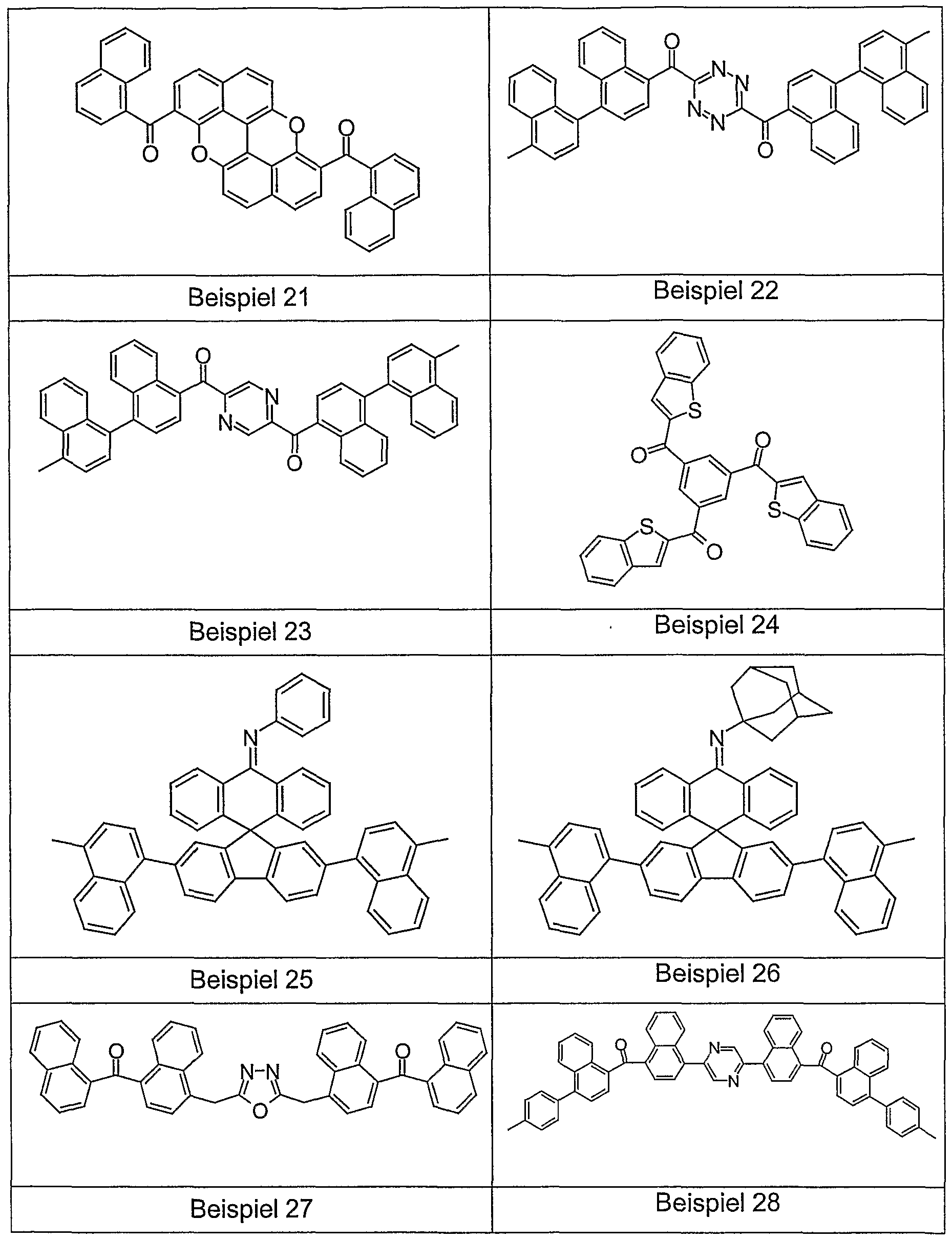
- Examples of preferred compounds of the formula (1) or of the formulas (2) to (4) are the following Examples 1 to 28:
- the compound of the formula (1) is preferably used as an electron transport material in an electron transport layer or in an emission layer.
- the compound of the formula (1) is particularly preferably used as an electron transport material in an electron transport layer.
- On Electron transport material is a material that predominantly conducts electrons in the electronic device.
- An organic electronic device is furthermore preferred, characterized in that the layer which contains the compound of the formula (1) comprises at least 50%, preferably at least 80% of this compound and very particularly preferably only the compound of the formula (1) exists as a clean layer.
- the use of a mixture of the compound of the formula (1) and further compounds can also be preferred.
- the other compounds can be both organic and inorganic, for example doping with a base metal, such as. B. alkali and / or alkaline earth metals, or with an organometallic compound such as. B. Co (Cp) 2 or Ni (Cp) 2 .
- the organic electronic device can also contain further layers. These can be, for example: hole injection layer, hole transport layer, emission layer, hole blocking layer, electron transport layer and / or electron injection layer.
- the presence of at least one emission layer is obligatory in an organic electroluminescent device. At this point, however, it should be pointed out that it is not necessary for each of the layers mentioned above to be present.
- a preferred aspect of the invention is an organic electroluminescent device according to the invention, comprising at least one electron transport layer between the fluorescent emission layer and the cathode, characterized in that the electron transport material contains at least one compound of the formula (1).
- the layer thickness of the electron transport layer is preferably between 5 and 500 nm, particularly preferably between 10 and 100 nm, very particularly preferably between 20 and 70 nm.
- an organic electroluminescent device characterized in that the emitter or emitters in the emission layer with suitable excitation in the visible spectral range with one or more maxima between 380 nm and 750 nm fluoresce. It may also be preferred if the emitters have several different emission maxima, so that white emission results overall.
- an organic electronic device characterized in that one or more layers are coated with a sublimation process.
- the materials are evaporated in vacuum sublimation systems at a pressure of less than 10 "5 mbar, preferably less than 10 " 6 mbar, particularly preferably less than 10 "7 mbar.
- An organic electronic device is also preferred, characterized in that one or more layers are coated with the OVPD (Organic Vapor Phase Deposition) process or with the aid of a carrier gas sublimation.
- the materials are applied at a pressure between 10 "5 mbar and 1 bar.
- an organic electronic device characterized in that one or more layers of solution, such as. B. by spin coating, or with any printing method, such as. B. screen printing, flexographic printing or offset printing, but particularly preferably LITI (Light Induced Thermal Imaging, thermal transfer printing) or ink-jet printing (ink jet printing).
- LITI Light Induced Thermal Imaging, thermal transfer printing
- ink-jet printing ink jet printing
- blue OLEDs can be represented in better color purity, since the compounds of the formula (1) are colorless and do not impair the efficiency and the color of the OLED by reabsorption. 5. Since the compounds of the formula (1) are generally not hygroscopic, they can be processed more easily and with less technical effort compared to AIQ 3 .
- the compounds according to formula (1) have a higher charge carrier mobility than electron transport materials according to the prior art, such as. B. AIQ 3 .
- thicker electron transport layers can be used. As already described above, this is important for avoiding short circuits and is furthermore particularly necessary for the combination of fluorescent and phosphorescent OLEDs in a display, since the thicker layer thicknesses of the phosphorescent OLEDs must be compensated for by a thicker electron transport layer of the fluorescent OLEDs.
- the main target is organic light-emitting diodes and the corresponding displays.
- compounds of the formula (1) also for other, related devices, for. B. for organic solar cells, organic thin film transistors, organic field-effect transistors or organic laser diodes to use.
- the starting materials (solvent, zinc, zinc cyanide, tetrakis (triphenylphosphine) palladium (0), phenylmagnesium bromide solution, EDTA, 1-bromonaphthalene, 4-methyl-1-naphthalene boronic acid, n-BuLi solution 2.5 molar in ⁇ -hexane, N, N-dimethyl-carbamic acid chloride, 2,7-dibromofluorenone) were obtained from ALDRICH and ABCR. 1,3,5-tris (4-bromophenyl) benzene was prepared according to M.
- the absorption edge of E1 is 351 nm.
- the honey-like residue was suspended in 2000 ml of glacial acetic acid, with 10 ml of conc. Hydrochloric acid added and heated under reflux for 5 h.
- the precipitated solid was filtered off from the warm reaction mixture (80 ° C.) and washed with 200 ml of glacial acetic acid.
- the solid was recrystallized again from 1000 ml of glacial acetic acid. Yield: 198.7 g (407 mmol), corresponding to 81.4% of theory. Th., Purity 97% (according to NMR).
- the precipitated solid was filtered off with suction, washed with 100 ml of water and ethanol each time and dried.
- the solid was placed in a Soxhlett extractor and extracted with chloroform through a glass fiber extraction thimble (pore size 0.1 ⁇ m).
- the chloroform was concentrated to a volume of 100 ml and 500 ml of ethanol were added.
- the resulting precipitate was filtered off and washed with ethanol.
- Tm 329 ° C
- T g 139 ° C.
- the yield of the electron transport material E3 was 36.9 g (59 mmol), corresponding to 78.7 % of theory, with a purity of> 99.9% (according to HPLC).
- OLEDs were produced by a general process according to WO 04/058911, which had to be adapted to the particular circumstances in each individual case (e.g. layer thickness variation in order to achieve optimum efficiency or color).
- the results of various OLEDs are presented in the following examples.
- HIL Hole injection layer
- PEDOT poly (3,4-ethylenedioxy-2,5-thiophene) hole transport layer
- HTM hole transport layer 20 nm NaphDATA (evaporated; obtained from SynTec; 4,4 ', 4 "tris (N-1-naphthyl-N-phenylamino) triphenylamine hole transport layer (HTM) 20 nm S-TAD (evaporated; produced according to WO 99/12888; 2,2 ', 7,7'-tetrakis (diphenylamino) -spiro- 9,9'-bifluorene) emission layer (EML) Spiro-DPVBi (manufactured according to WO 02/10093, 2,2', 7,7'-tetrakis (2,2'-diphenylvinyl) -spiro-9,
- OLEDs which have not yet been optimized, have been characterized as standard; For this purpose, the electroluminescence spectra, the efficiency (measured in cd / A), the power efficiency (measured in Im / W) depending on the brightness, calculated from current-voltage-brightness characteristics (IUL characteristics), and the service life were determined.
- the lifetime is defined as the time after which the initial brightness of the OLED has halved at a constant current density of 10 mA / cm 2 .
- the layer thickness was optimized separately for each material for the electron transport layer. For a better comparison, however, the thicker AIQ 3 layer thicknesses are also listed, which are directly comparable with the layer thicknesses of E1 and E2.
- the composition of the ETL including the layer thicknesses being listed in each case.
- the ETLs contain the compounds E1 as electron transport material to E4.
- OLEDs which contain AIQ 3 as the electron conductor according to the prior art serve as comparative examples.
- All OLEDs show blue emission, which comes from the fluorescence emitter S-DPVBi. Higher photometric efficiencies are obtained in devices in which the AIQ 3 electron conductor has been replaced by the electron conductors E1 to E4 according to the invention. Since the voltages required to achieve a certain brightness are also low here, very good power efficiency is obtained.
- the service life increases from approx. 650 h to over 1100 h. In particular, with the same layer thickness of the ETL, the efficiencies, the power efficiencies, the service life and the color are better with the electron transport materials according to the invention than with the standard electron conductor AIQ 3 .
- OLEDs manufactured according to the new design principle, have a higher efficiency at lower voltages and a longer service life, as can easily be seen in Table 1.
Landscapes
- Chemical & Material Sciences (AREA)
- Organic Chemistry (AREA)
- Physics & Mathematics (AREA)
- Engineering & Computer Science (AREA)
- Materials Engineering (AREA)
- Spectroscopy & Molecular Physics (AREA)
- Optics & Photonics (AREA)
- Electroluminescent Light Sources (AREA)
- Organic Low-Molecular-Weight Compounds And Preparation Thereof (AREA)
Abstract
Description
Beschreibungdescription
Organische elektronische VorrichtungenOrganic electronic devices
Die vorliegende Erfindung beschreibt den Einsatz bestimmter Verbindungen in organischen elektronischen Vorrichtungen.The present invention describes the use of certain compounds in organic electronic devices.
In einer Reihe verschiedenartiger Anwendungen, die im weitesten Sinne der Elektronikindustrie zugerechnet werden können, ist der Einsatz organischer Halbleiter seit geraumer Zeit Realität bzw. wird in naher Zukunft erwartet. Der Einsatz halbleitender organischer Verbindungen, die zur Emission von Licht im sichtbaren Spektralbereich befähigt sind, steht gerade am Anfang der Markteinführung, zum Beispiel in organischen Elektrolumineszenzvorrichtungen. Für einfache OLEDs enthaltende Vorrichtungen ist die Markteinführung bereits erfolgt, wie die Autoradios der Firma Pioneer, die Mobiltelefone der Firmen Pioneer und SNMD und eine Digitalkamera der Firma Kodak mit "organischem Display" belegen. Weitere derartige Produkte stehen kurz vor der Einführung. Organische Solarzellen (O-SCs), organische Feldeffekt-Transistoren (O-FETs), organische Dünnfilmtransistoren (O-TFTs), organische Schaltelemente (O-ICs), organische optische Verstärker oder organische Laserdioden (O-Laser) sind in einem Forschungsstadium weit fortgeschritten und könnten in der Zukunft große Bedeutung erlangen.In a number of different applications, which can be broadly attributed to the electronics industry, the use of organic semiconductors has been a reality for some time or is expected in the near future. The use of semiconducting organic compounds that are capable of emitting light in the visible spectral range is just at the beginning of the market launch, for example in organic electroluminescent devices. The market launch for simple devices containing OLEDs has already taken place, as evidenced by the car radios from Pioneer, the mobile phones from Pioneer and SNMD and a digital camera from Kodak with an "organic display". Other such products are about to be launched. Organic solar cells (O-SCs), organic field effect transistors (O-FETs), organic thin-film transistors (O-TFTs), organic switching elements (O-ICs), organic optical amplifiers or organic laser diodes (O-lasers) are far in the research stage advanced and could become very important in the future.
Der allgemeine Aufbau organischer Elektrolumineszenzvorrichtungen (OLEDs) ist beispielsweise in US 4,539,507, US 5,151 ,629, EP 0676461 , WO 98/27136 und in WO 04/058911 beschrieben, wobei diese Vorrichtungen üblicherweise aus mehreren Schichten bestehen. Organische Solarzellen (z. B. WO 98/48433, WO 94/05045), organische Feld-Effekt-Transistoren (z. B. US 5705826, US 5596208, WO 00/42668), organische Dünnschichttransistoren, organische Schaltelemente (z. B. WO 95/31833, WO 99/10939), organische optische Verstärker oder organische Laserdioden (z. B. WO 98/03566) weisen einen ähnlichen allgemeinen Aufbau auf.The general structure of organic electroluminescent devices (OLEDs) is described, for example, in US 4,539,507, US 5,151, 629, EP 0676461, WO 98/27136 and WO 04/058911, these devices usually consisting of several layers. Organic solar cells (e.g. WO 98/48433, WO 94/05045), organic field-effect transistors (e.g. US 5705826, US 5596208, WO 00/42668), organic thin-film transistors, organic switching elements (e.g. WO 95/31833, WO 99/10939), organic optical amplifiers or organic laser diodes (e.g. WO 98/03566) have a similar general structure.
Allerdings gibt es immer noch erhebliche Probleme, die einer dringenden Verbesserung bedürfen:However, there are still significant problems that need urgent improvement:
1. Die Effizienz ist in den letzten Jahren verbessert worden, ist aber gerade bei bei fluoreszierenden OLEDs immer noch zu niedrig und muß verbessert werden.1. The efficiency has been improved in recent years, but is still too low, especially in the case of fluorescent OLEDs, and must be improved.
2. Die Betriebsspannung und der Betriebsstrom sind gerade bei fluoreszierenden OLEDs recht hoch und müssen daher weiter verringert werden, um die2. The operating voltage and the operating current are quite high, especially in the case of fluorescent OLEDs, and must therefore be reduced further in order to
BESTATIGUNGSKOPIE Leistungseffizienz zu verbessern. Das ist gerade für mobile Anwendungen von großer Bedeutung.BESTATIGUNGSKOPIE Improve performance efficiency. This is particularly important for mobile applications.
3. Die operative Lebensdauer der elektronischen Vorrichtungen ist immer noch gering, so daß bis dato nur einfache Anwendungen kommerziell realisiert werden konnten.3. The operational life of the electronic devices is still short, so that only simple applications could be realized commercially until now.
4. Für viele Anwendungen, wie unten beschrieben, werden dickere Elektronentransportschichten benötigt, als sie mit den derzeit verwendeten Materialien realisiert werden können, da die Ladungsträgerbeweglichkeit dieser Materialien nicht ausreicht.4. For many applications, as described below, thicker electron transport layers are required than can be achieved with the materials currently used, since the charge carrier mobility of these materials is insufficient.
5. Der meist verwendete Elektronenleiter AIQ3 hat verschiedene Nachteile, die unten detailliert ausgeführt werden.5. The most commonly used AIQ 3 electron conductor has several disadvantages, which are detailed below.
Für viele Anwendungen wäre es wünschenswert, dickere Schichten eines Elektronentransportmaterials verwenden zu können. Dies hätte den Vorteil, daß dadurch das Auftreten von Kurzschlüssen verringert bzw. ganz verhindert werden könnte. Weiterhin gilt dies insbesondere, wenn eine Kombination aus fluoreszierenden blauen und phosphoreszierenden roten und grünen OLEDs in Displays verwendet wird. Da die phosphoreszierenden OLEDs im allgemeinen eine dickere Schichtstruktur aufweisen, muß die fluoreszierende blaue OLED eine dickere Elektronentransportschicht enthalten, damit die unterschiedlichen OLEDs die gleiche Gesamtdicke aufweisen. Da jedoch die Elektronenbeweglichkeit der Elektronentransportverbindungen gemäß dem Stand der Technik hierfür nicht ausreicht, ist dies in der Praxis noch nicht möglich.For many applications it would be desirable to be able to use thicker layers of an electron transport material. This would have the advantage that the occurrence of short circuits could be reduced or prevented altogether. This is especially true when a combination of fluorescent blue and phosphorescent red and green OLEDs is used in displays. Since the phosphorescent OLEDs generally have a thicker layer structure, the fluorescent blue OLED must contain a thicker electron transport layer so that the different OLEDs have the same overall thickness. However, since the electron mobility of the electron transport compounds according to the prior art is not sufficient for this, this is not yet possible in practice.
Elektrolumineszenzvorrichtungen, die AIQ3 als Elektronenleiter verwenden, wurden schon 1983 in US 4,539,507 beschrieben; AIQ3 wird seither in den meisten OLEDs als Elektronentransportmaterial eingesetzt. In der oben genannten Anmeldung wird es als Elektronentransportmaterial in der Emissionsschicht verwendet. AIQ3 hat allerdings mehrere Nachteile: Es läßt sich nicht rückstandsfrei aufdampfen, da es sich bei der Sublimationstemperatur teilweise zersetzt, was insbesondere für Produktionsanlagen ein großes Problem darstellt. Dies hat zur Folge, daß die Aufdampfquellen immer wieder gereinigt oder gewechselt werden müssen. Des weiteren gelangen Zersetzungsprodukte von AIQ3 in die OLED, die dort zu einer verringerten Lebensdauer und reduzierten Quanten- und Leistungseffizienz beitragen. Ein entscheidender praktischer Nachteil ist die starke Hygroskopie von AIQ3. Unter normalen Bedingungen synthetisiert und aufbewahrt, enthält AIQ3 neben den Hydroxychinolin-Liganden immer noch ein Molekül Wasser pro Komplexmolekül (H. Schmidbaur et al., Z. Naturforsch. 1991 , 46b, 901-911), welches extrem schwer zu entfernen ist. Für die Verwendung in OLEDs muß AIQ3 deshalb in komplizierten, mehrstufigen Sublimationsverfahren aufwendig gereinigt und im Anschluß daran unter Wasserausschluß in einer Schutzgasatmosphäre gelagert und gehandhabt werden. Weiterhin wurden große Schwankungen in der Qualität einzelner AIQ3-Chargen, sowie eine schlechte Lagerstabilität festgestellt (S. Karg, E-MRS Konferenz 30.5.00-2.6.00, Straßburg). AIQ3 hat außerdem eine niedrige Elektronenbeweglichkeit, was zu höheren Spannungen und damit zu einer niedrigeren Leistungseffizienz führt. Um Kurzschlüsse im Display zu vermeiden, würde man, wie oben beschrieben, gern die Schichtdicke erhöhen; dies ist mit AIQ3 wegen der geringen Ladungsträgerbeweglichkeit und der daraus resultierenden Spannungserhöhung nicht möglich. Die Ladungsträgerbeweglichkeit anderer Elektronenleiter (US 4,539,507) ist ebenfalls zu gering, um dickere Schichten damit aufzubauen, wobei die Lebensdauer der OLED noch schlechter ist als bei Verwendung von AIQ3. Als sehr ungünstig erweist sich weiterhin die Eigenfarbe von AIQ3 (im Feststoff gelb), die gerade bei blauen OLEDs durch Reabsorption und schwache Reemission zu Farbverschiebungen führen kann. Hier sind blaue OLEDs nur mit starken Effizienz- bzw. Farborteinbußen darstellbar. Weiterer Nachteil des Einsatzes von AIQ3 ist die Instabilität gegenüber Löchern (Z. Popovic et al., Proceedings of SPIE 1999, 3797, 310-315), was bei einem Langzeiteinsatz immer zu Problemen im Bauelement führen kann. Trotz der genannten Nachteile stellt AIQ3 in OLEDs bislang immer noch den besten Kompromiß für die verschiedenartigen Anforderungen an ein Elektronentransportmaterial in OLEDs dar. Auch für die anderen genannten Anwendungen wurde bislang noch kein zufriedenstellendes Elektronentransportmaterial gefunden.Electroluminescent devices which use AIQ 3 as an electron conductor have already been described in US 4,539,507 in 1983; Since then, AIQ 3 has been used in most OLEDs as an electron transport material. In the above application, it is used as an electron transport material in the emission layer. However, AIQ 3 has several disadvantages: It cannot be vapor-deposited without residue, since it partially decomposes at the sublimation temperature, which is a major problem especially for production plants. As a result, the evaporation sources have to be cleaned or replaced again and again. Furthermore, decomposition products from AIQ 3 get into the OLED, which contribute to a reduced lifespan and reduced quantum and power efficiency. A major practical disadvantage is the strong hygroscopy of AIQ 3 . Synthesized and stored under normal conditions, in addition to the hydroxyquinoline ligands, AIQ 3 still contains one molecule of water per complex molecule (H. Schmidbaur et al., Z. Naturforsch. 1991, 46b, 901-911), which is extremely heavy is to be removed. For use in OLEDs, AIQ 3 must therefore be laboriously cleaned in complicated, multi-stage sublimation processes and then stored and handled in a protective gas atmosphere with the exclusion of water. Furthermore, large fluctuations in the quality of individual AIQ 3 batches and poor storage stability were found (S. Karg, E-MRS conference May 30-26, 00, Strasbourg). AIQ 3 also has low electron mobility, which leads to higher voltages and thus lower power efficiency. In order to avoid short circuits in the display, one would like to increase the layer thickness, as described above; this is not possible with AIQ 3 due to the low mobility of the charge carriers and the resulting increase in voltage. The charge carrier mobility of other electron conductors (US Pat. No. 4,539,507) is also too low to build up thicker layers with it, the lifetime of the OLED being even worse than when using AIQ 3 . The intrinsic color of AIQ 3 (yellow in the solid) also proves to be very unfavorable, which can lead to color shifts due to reabsorption and poor re-emission, especially with blue OLEDs. Here, blue OLEDs can only be produced with a significant loss of efficiency or color location. Another disadvantage of using AIQ 3 is the instability towards holes (Z. Popovic et al., Proceedings of SPIE 1999, 3797, 310-315), which can always lead to problems in the component during long-term use. Despite the disadvantages mentioned, AIQ 3 in OLEDs has so far still been the best compromise for the different requirements for an electron transport material in OLEDs. No satisfactory electron transport material has yet been found for the other applications mentioned.
Die Verwendung bestimmter Ketone in OLEDs ist bereits vereinzelt in der Literatur beschrieben worden (z. B. JP 6192654 oder JP 406100857). Jedoch haben auch die dort verwendeten Verbindungen den Nachteil, daß sie eine Eigenfarbe aufweisen, die gerade bei blauen OLEDs durch Reabsorption zu Farbverschiebungen bzw. zumindest zu reduzierter Effizienz führt. Die bekannten Verbindungen stellen also keinen Vorteil gegenüber AIQ3 für die Verwendung in blauen OLEDs dar. Da es für die technische Herstellung von OLEDs bevorzugt ist, für alle Farben denselben Elektronenleiter zu verwenden, stellen diese Verbindungen auch für die anderen Emissionsfarben keine brauchbare Alternative zu AIQ3 dar.The use of certain ketones in OLEDs has already been described in isolated cases in the literature (for example JP 6192654 or JP 406100857). However, the compounds used there also have the disadvantage that they have an inherent color which, particularly in the case of blue OLEDs, leads to color shifts or at least to reduced efficiency due to reabsorption. The known compounds therefore do not represent any advantage over AIQ 3 for use in blue OLEDs. Since it is preferred for the technical production of OLEDs to use the same electron conductor for all colors, these compounds also do not represent a useful alternative to AIQ for the other emission colors 3 represents.
Es besteht also weiterhin der Bedarf an Elektronentransportmaterialien, die in organischen elektronischen Vorrichtungen zu guten Effizienzen und gleichzeitig zu hohen Lebensdauern führen. Es wurde nun überraschend gefunden, daß organische elektronische Vorrichtungen, die bestimmte - im folgenden aufgeführte - Verbindungen als Elektronentransportmaterialien enthalten, deutliche Verbesserungen gegenüber dem Stand der Technik aufweisen. Mit diesen Materialien ist es möglich, gleichzeitig hohe Effizienzen und lange Lebensdauern zu erhalten, was mit Materialien gemäß dem Stand der Technik nicht möglich ist. Zudem wurde gefunden, daß zusätzlich die Betriebsspannungen deutlich gegenüber AIQ3 gesenkt werden können, was höheren Leistungseffizienzen entspricht, und daß dickere Elektronentransportschichten verwendet werden können, was die Häufigkeit von Kurzschlüssen reduziert bzw. verhindert und weitere, oben ausgeführte, Vorteile mit sich bringt.So there is still a need for electron transport materials that are both efficient and efficient in organic electronic devices lead to long lifetimes. It has now surprisingly been found that organic electronic devices which contain certain compounds - listed below - as electron transport materials have significant improvements over the prior art. With these materials it is possible to obtain high efficiencies and long lifetimes at the same time, which is not possible with materials according to the prior art. In addition, it was found that the operating voltages can also be significantly reduced compared to AIQ 3 , which corresponds to higher power efficiencies, and that thicker electron transport layers can be used, which reduces or prevents the frequency of short circuits and has other advantages, as outlined above.
Gegenstand der Erfindung ist eine organische elektronische Vorrichtung, enthaltend Kathode, Anode und mindestens eine organische Schicht, dadurch gekennzeichnet, daß die organische Schicht mindestens eine Verbindung gemäß Formel (1 ) enthält,The invention relates to an organic electronic device containing cathode, anode and at least one organic layer, characterized in that the organic layer contains at least one compound of the formula (1),

X ist bei jedem Auftreten gleich oder verschieden O, S, Se, Te oder NR;X is the same or different on each occurrence O, S, Se, Te or NR;
R ist bei jedem Auftreten gleich oder verschieden ein organischer Rest mit 1 bis 22 Kohlenstoffatomen, der auch über ein O- oder N-Atom an X gebunden sein kann, oder OH oder NH2;R is the same or different at each occurrence an organic radical having 1 to 22 carbon atoms, which can also be bonded to X via an O or N atom, or OH or NH 2 ;
R1, R2 ist bei jedem Auftreten gleich oder verschieden ein aromatisches oder heteroaromatisches Ringsystem mit 1 bis 40 aromatischen C-Atomen, das durch einen oder mehrere Reste R3 substituiert sein kann, wobei die Substituenten R1 und R2 miteinander ein mono- oder polycyclisches Ringsystem bilden können;Each occurrence of R 1 , R 2 is identical or different to an aromatic or heteroaromatic ring system with 1 to 40 aromatic C atoms, which can be substituted by one or more radicals R 3 , the substituents R 1 and R 2 being a mono- or can form polycyclic ring system;
R3 ist bei jedem Auftreten gleich oder verschieden H, OH, N(R )2, CN, B(R4)2, Si(R4)3, eine geradkettige, verzweigte oder cyclische Alkyl- oder Alkoxykette mit 1 bis 22 C-Atomen, in der auch ein oder mehrere nicht benachbarte C-Atome durch -R4C=CR4-, -C ≡€-, Si(R4)2, Ge(R4)2, Sn(R4)2> -NR4-, -O-, -S-, -CO-, -CO-O-, -O-CO-O- ersetzt sein können, wobei auch ein oder mehrere H-Atome durch Fluor ersetzt sein können, oder eine Aryl-, Heteroaryl- oder Aryloxygruppe mit 1 bis 40 C-Atomen, welche auch durch einen oder mehrere Reste R4 substituiert sein kann, oder eine Kombination aus 2, 3 oder 4 dieser Systeme; dabei können zwei oder mehrere Reste R3 auch miteinander ein Ringsystem bilden; R4 ist bei jedem Auftreten gleich oder verschieden H oder ein aliphatischer oder aromatischer Kohlenwasserstoffrest mit 1 bis 20 C-Atomen; n ist bei jedem Auftreten 1 , 2, 3, 4, 5, 6, 7, 8, 9 oder 10; mit der Maßgabe, daß die Verbindung gemäß Formel (1 ) ein Molekulargewicht von > 150 g/mol und < 10000 g/mol aufweist und daß die Vorrichtung keinen phosphoreszierenden Emitter enthält; und weiterhin mit der Maßgabe, daß weder R 1 noch R2 ein substituiertes oder unsubstituiertes Spirobifluoren darstellt, dadurch gekennzeichnet, daß die Absorptionskante der Verbindung gemäß Formel (1) < 400 nm ist.Each occurrence of R 3 is the same or different H, OH, N (R) 2 , CN, B (R 4 ) 2 , Si (R 4 ) 3 , a straight-chain, branched or cyclic alkyl or alkoxy chain with 1 to 22 C. -Atoms in which one or more non-adjacent C atoms are represented by -R 4 C = CR 4 -, -C ≡ € -, Si (R 4 ) 2 , Ge (R 4 ) 2 , Sn (R 4 ) 2 > -NR 4 -, -O-, -S-, -CO-, -CO-O-, -O-CO-O- can be replaced, wherein one or more H atoms can also be replaced by fluorine, or an aryl, heteroaryl or aryloxy group with 1 to 40 C atoms, which can also be substituted by one or more R 4 radicals, or a combination of 2, 3 or 4 of these systems; two or more R 3 radicals can also form a ring system with one another; Each occurrence of R 4 is the same or different H or an aliphatic or aromatic hydrocarbon radical having 1 to 20 C atoms; n is 1, 2, 3, 4, 5, 6, 7, 8, 9 or 10 at each occurrence; with the proviso that the compound of formula (1) has a molecular weight of> 150 g / mol and <10000 g / mol and that the device contains no phosphorescent emitter; and further provided that neither R 1 nor R 2 is a substituted or unsubstituted spirobifluorene, characterized in that the absorption edge of the compound of formula (1) is <400 nm.
Unter Absorptionskante im Sinne dieser Erfindung wird folgendes verstanden: Legt man in die längerwellige Flanke der langwelligsten Absorptionsbande zwischen Singulettzuständen des Absorptionsspektrums (also ein So -» S-i-Übergang) einer Schicht dieser Verbindung mit einer Schichtdicke von 100 nm eine Wendetangente und bestimmt den Schnittpunkt dieser Wendetangente mit der Abszisse, so ergibt die so erhaltene Wellenlänge die Absorptionskante der Verbindung.Absorption edge in the sense of this invention is understood to mean the following: if a turning tangent is placed in the longer-wave flank of the long-wave absorption band between singlet states of the absorption spectrum (thus a So - »Si transition) of a layer of this compound with a layer thickness of 100 nm and the intersection of this is determined Turn tangent with the abscissa, the wavelength obtained in this way gives the absorption edge of the compound.
Bevorzugt ist die Absorptionskante der Verbindung gemäß Formel (1 ) < 380 nm.The absorption edge of the compound of the formula (1) is preferably <380 nm.
Unter einem aromatischen oder heteroaromatischen Ringsystem im Sinne dieser Erfindung soll ein System verstanden werden, das nicht notwendigerweise nur aromatische bzw. heteroaromatische Gruppen enthält, sondern in dem auch zwei oder mehrere aromatische oder heteroaromatische Gruppen durch eine kurze, nicht aromatische Einheit (bevorzugt < 10 % der von H verschiedenen Atome, besonders bevorzugt < 5 % der von H verschiedenen Atome), wie z. B. ein sp3-hybridisiertes C-, N- oder O-Atom, unterbrochen sein können. So sollen also beispielsweise auch Systeme wie 9,9-DiaryIfluoren, Triarylamin, etc. als aromatische Systeme im Sinne dieser Anmeldung verstanden werden.An aromatic or heteroaromatic ring system in the sense of this invention is to be understood as meaning a system which does not necessarily only contain aromatic or heteroaromatic groups, but also in which two or more aromatic or heteroaromatic groups by a short, non-aromatic unit (preferably <10% the atoms different from H, particularly preferably <5% of the atoms different from H), such as. B. an sp 3 hybridized C, N or O atom may be interrupted. Thus, for example, systems such as 9,9-diarylfluorene, triarylamine, etc. should also be understood as aromatic systems in the sense of this application.
Im Rahmen der vorliegenden Erfindung werden unter einer Ci- bis C22-Alkylgruppe, in der auch einzelne H-Atome oder CH2-Gruppen durch die oben genannten Gruppen substituiert sein können, besonders bevorzugt die Reste Methyl, Ethyl, n-Propyl, i-Propyl, n-Butyl, i-Butyl, s-Butyl, t-Butyl, 2-Methylbutyl, n-Pentyl, s-Pentyl, Cyclopentyl, n-Hexyl, Cyclohexyl, n-Heptyl, Cycloheptyl, n-Octyl, Cyclooctyl, 2-Ethylhexyl, Trifluormethyl, Pentafluorethyl, 2,2,2-Trifluorethyl, Ethenyl, Propenyl, Butenyl, Pentenyl, Cyclopentenyl, Hexenyl, Cyclohexenyl, Heptenyl, Cycloheptenyl, Octenyl, Cyclooctenyl, Ethinyl, Propinyl, Butinyl, Pentinyl, Hexinyl oder Octinyl verstanden. Unter einer C-i- bis C22-Alkoxygruppe werden besonders bevorzugt Methoxy, Ethoxy, n-Propoxy, i-Propoxy, n-Butoxy, i-Butoxy, s-Butoxy, t-Butoxy oder 2-Methylbutoxy verstanden. Unter einem C-ι-C o aromatischen oder heteroaromatischen Ringsystem, das noch jeweils mit den oben genannten Resten R3 substituiert sein kann, werden insbesondere Gruppen verstanden, welche abgeleitet sind von Benzol, Naphthalin, Biphenylen, Terphenylen, Fluoren, Dihydrophenanthren, Tetrahydropyren, eis- oder trans-lndenofluoren, Furan, Benzofuran, Isobenzofuran, Dibenzofuran, Thiophen, Benzothiophen, Isobenzothiophen, Dibenzothiophen, Pyrrol, Indol, Isoindol, Carbazol, Pyridin, Chinolin, Isochinolin, Acridin, Phenanthridin, Benzo-5,6-chinolin, Benzo-6,7-chinolin, Benzo-7,8-chinolin, Phenothiazin, Phenoxazin, Pyrazol, Indazol, Imidazol, Benzimidazol, Naphthimidazol, Phenanthrimidazol, Pyridimidazol, Pyrazinimidazol, Chinoxalinimidazol, Oxazol, Benzoxazol, Naphthoxazol, Anthroxazol, Phenanthroxazol, Isoxazol, 1 ,2-Thiazol, 1,3-Thiazol, Benzothiazol, Pyridazin, Benzopyridazin, Pyrimidin, Benzpyrimidin, Chinoxalin, Pyrazin, Phenazin, Naphthyridin, Azacarbazol, Benzocarbolin, Phenanthrolin, 1,2,3-Triazol, 1,2,4- Triazol, Benzotriazol, 1 ,2,3-Oxadiazol, 1 ,2,4-Oxadiazol, 1 ,2,5-Oxadiazol, 1 ,3,4- Oxadiazol, 1 ,2,3-Thiadiazol, 1,2,4-Thiadiazol, 1 ,2,5-Thiadiazol, 1 ,3,4-Thiadiazol, 1 ,3,5-Triazin, 1 ,2,4-Triazin, 1 ,2,3-Triazin, Tetrazol, 1 ,2,4,5-Tetrazin, 1 ,2,3,4-Tetrazin, 1 ,2,3,5-Tetrazin, Purin, Pteridin, Indolizin und Benzothiadiazol.In the context of the present invention, the radicals methyl, ethyl, n-propyl, i. Are particularly preferred under a Ci to C 22 alkyl group, in which individual H atoms or CH 2 groups can also be substituted by the abovementioned groups Propyl, n-butyl, i-butyl, s-butyl, t-butyl, 2-methylbutyl, n-pentyl, s-pentyl, cyclopentyl, n-hexyl, cyclohexyl, n-heptyl, cycloheptyl, n-octyl, cyclooctyl , 2-ethylhexyl, trifluoromethyl, pentafluoroethyl, 2,2,2-trifluoroethyl, ethenyl, propenyl, Butenyl, pentenyl, cyclopentenyl, hexenyl, cyclohexenyl, heptenyl, cycloheptenyl, octenyl, cyclooctenyl, ethynyl, propynyl, butynyl, pentynyl, hexynyl or octynyl. A Ci to C 22 alkoxy group is particularly preferably understood to mean methoxy, ethoxy, n-propoxy, i-propoxy, n-butoxy, i-butoxy, s-butoxy, t-butoxy or 2-methylbutoxy. A C 1 -C 8 aromatic or heteroaromatic ring system, which can in each case be substituted with the abovementioned R 3 radicals, is understood in particular to mean groups which are derived from benzene, naphthalene, biphenylene, terphenylene, fluorene, dihydrophenanthrene, tetrahydropyrene, ice or trans-indofluorene, furan, benzofuran, isobenzofuran, dibenzofuran, thiophene, benzothiophene, isobenzothiophene, dibenzothiophene, pyrrole, indole, isoindole, carbazole, pyridine, quinoline, isoquinoline, acridine, phenanthridine, benzo-5,6-quinoline, benzo -6,7-quinoline, benzo-7,8-quinoline, phenothiazine, phenoxazine, pyrazole, indazole, imidazole, benzimidazole, naphthimidazole, phenanthrimidazole, pyridimidazole, pyrazinimidazole, quinoxaline imidazole, oxazole, benzoxazole, naphthazoloxazol, naphthazoloxazol, naphthazoloxazole, , 2-thiazole, 1,3-thiazole, benzothiazole, pyridazine, benzopyridazine, pyrimidine, benzpyrimidine, quinoxaline, pyrazine, phenazine, naphthyridine, azacarbazole, benzocarboline, phenanthrol in, 1,2,3-triazole, 1,2,4-triazole, benzotriazole, 1, 2,3-oxadiazole, 1, 2,4-oxadiazole, 1, 2,5-oxadiazole, 1, 3,4- Oxadiazole, 1, 2,3-thiadiazole, 1,2,4-thiadiazole, 1, 2,5-thiadiazole, 1, 3,4-thiadiazole, 1, 3,5-triazine, 1, 2,4-triazine, 1, 2,3-triazine, tetrazole, 1, 2,4,5-tetrazine, 1, 2,3,4-tetrazine, 1, 2,3,5-tetrazine, purine, pteridine, indolizine and benzothiadiazole.
Elektronische Vorrichtungen im Sinne dieser Erfindung sind bevorzugt organische Elektrolumineszenzvorrichtungen (organische Leuchtdioden, OLEDs), organische Dünnfilmtransistoren (O-TFTs), organische Feld-Effekt-Transistoren (O-FETs), organische Solarzellen (O-SCs), organische Photorezeptoren oder organische Laser (O-Laser), insbesondere organische Elektrolumineszenzvorrichtungen.Electronic devices in the sense of this invention are preferably organic electroluminescent devices (organic light-emitting diodes, OLEDs), organic thin-film transistors (O-TFTs), organic field-effect transistors (O-FETs), organic solar cells (O-SCs), organic photoreceptors or organic lasers (O-laser), in particular organic electroluminescent devices.
Bevorzugt ist eine organische elektronische Vorrichtung, dadurch gekennzeichnet, daß die Verbindung gemäß Formel (1) amorph ist und die Glastemperatur Tg der Verbindung größer als 80 °C, besonders bevorzugt größer als 100 °C, insbesondere größer als 130 °C ist.An organic electronic device is preferred, characterized in that the compound of the formula (1) is amorphous and the glass transition temperature T g of the compound is greater than 80 ° C, particularly preferably greater than 100 ° C, in particular greater than 130 ° C.
Besonders bevorzugt ist eine organische elektronische Vorrichtung, dadurch gekennzeichnet, daß X für O oder NR steht, insbesondere für O. Ganz besonders bevorzugt sind organische elektronische Vorrichtungen, dadurch gekennzeichnet, daß die Verbindungen gemäß Formel (1 ) nur aus den Elementen Kohlenstoff, Wasserstoff und Sauerstoff bestehen.An organic electronic device is particularly preferred, characterized in that X stands for O or NR, in particular for O. Organic electronic devices are very particularly preferred, characterized in that the compounds of the formula (1) consist only of the elements carbon, hydrogen and oxygen.
Um eine Absorptionskante < 400 nm zu erreichen, ist es bevorzugt, wenn die Reste R1 und R2 keine kondensierten aromatischen Ringsysteme mit drei oder mehr kondensierten Benzoleinheiten, also beispielsweise kein Anthracen, Pyren, Phenanthren, Perylen, etc., enthalten. Bevorzugt sind also maximal zwei kondensierte Benzoleinheiten. Dies schließt jedoch nicht aus, daß diese Reste kondensierte heteroaromatische Ringsysteme mit drei od er mehr kondensierten Ringen enthalten können, beispielsweise Phenanthrolin, Acridin, etc..In order to achieve an absorption edge <400 nm, it is preferred if the radicals R 1 and R 2 contain no condensed aromatic ring systems with three or more condensed benzene units, that is to say for example no anthracene, pyrene, phenanthrene, perylene, etc. A maximum of two condensed benzene units are therefore preferred. However, this does not exclude that these residues can contain condensed heteroaromatic ring systems with three or more condensed rings, for example phenanthroline, acridine, etc.
Es kann auch bevorzugt sein, wenn die Verbindung gemäß Formel (1 ) mehr als eine Carbonylgruppe enthält. Dabei kann die Anordnung der Carbonylgruppen im Molekül linear oder auch verzweigt sein, bzw. sie können auch dendritisch angeordnet sein. Bevorzugt sind Verbindungen, die dend ritisch aufgebaut sind. Weiterhin bevorzugt sind 1 ,3,5-trisubstituierte Benzole. In diesem Fall stellt dann beispielsweise der Rest R1 eine verbrückende Gruppe zw ischen zwei oder mehr Carbonylfunktionen dar.It may also be preferred if the compound of the formula (1) contains more than one carbonyl group. The arrangement of the carbonyl groups in the molecule can be linear or branched, or they can also be arranged dendritic. Preference is given to compounds which have a denditic structure. 1,3,5-Trisubstituted benzenes are also preferred. In this case, for example, the radical R 1 then represents a bridging group between two or more carbonyl functions.
Bevorzugte Verbindungen gemäß Formel (1 ) sind die Verbindungen gemäß denPreferred compounds according to formula (1) are the compounds according to
Formeln (2) bis (4):Formulas (2) to (4):

Ar ist bei jedem Auftreten gleich oder verschieden ein bivalentes (in Formel (2)) bzw. ein trivalentes (in Formel (3)) aromatisches oder heteroaromatisches Ringsystem mit 3 bis 24 aromatischen C-Atomen, das durch einen oder mehrere Reste R3 substituiert sein kann; m ist bei jedem Auftreten gleich oder verschieden 1 , 2 oder 3. Dabei bedeutet m = 2 oder m = 3 eine lineare Verknüpfung von zwei oder drei Carbonylfunktionen über die Gruppe R2.Ar is the same or different at each occurrence, a bivalent (in formula (2)) or a trivalent (in formula (3)) aromatic or heteroaromatic ring system with 3 to 24 aromatic C atoms, which is substituted by one or more radicals R 3 can be; Each occurrence m is the same or different 1, 2 or 3. Here, m = 2 or m = 3 means a linear linkage of two or three carbonyl functions via the group R 2 .
Beispiele für bevorzugte Verbindungen gemäß Formel (1) bzw. gemäß den Formeln (2) bis (4) sind die folgenden Beispiele 1 bis 28:Examples of preferred compounds of the formula (1) or of the formulas (2) to (4) are the following Examples 1 to 28:
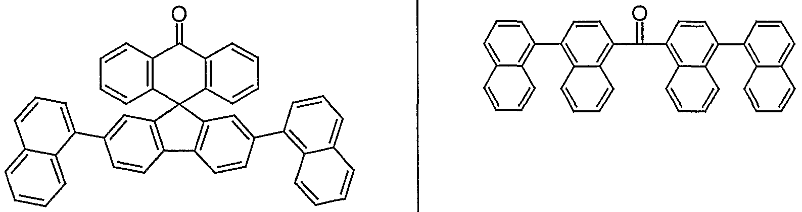


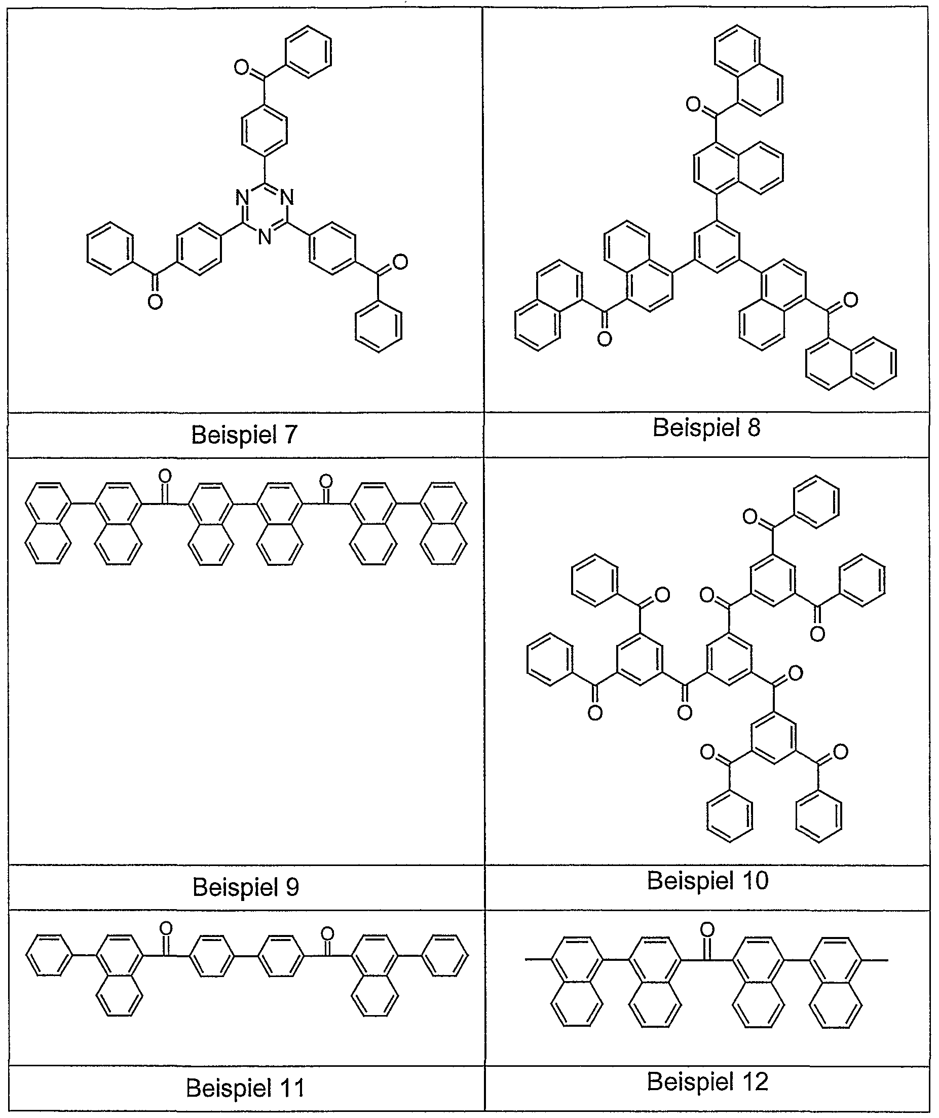

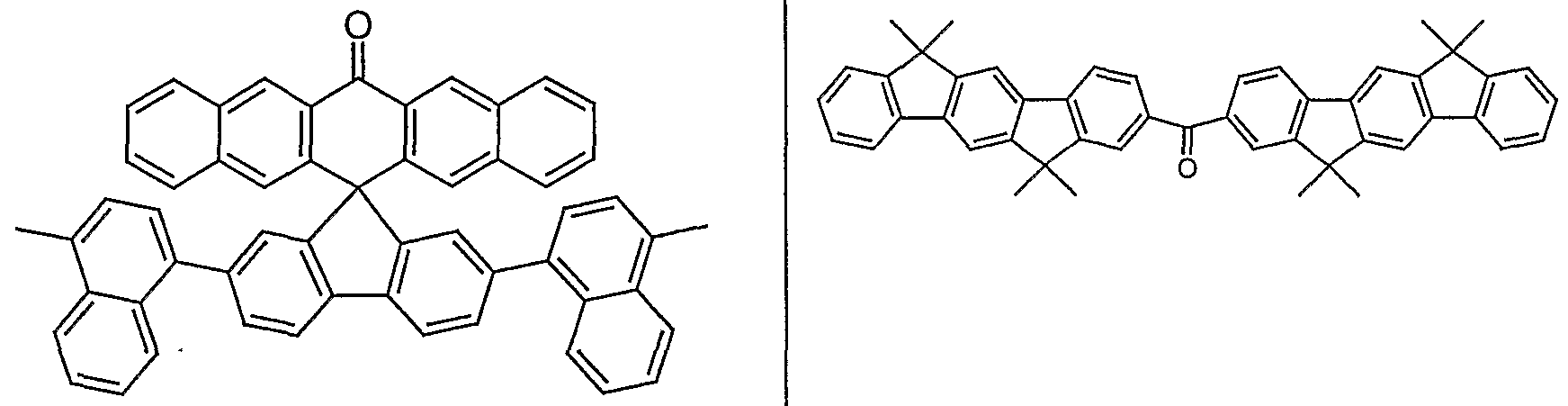
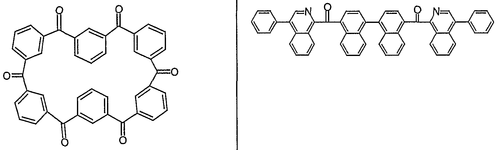

Beispiel 19 Beispiel 20
Bevorzugt wird die Verbindung gemäß Formel (1) als Elektronentransportmaterial in einer Elektronentransportschicht oder in einer Emissionsschicht eingesetzt. Besonders bevorzugt wird die Verbindung gemäß Formel (1 ) als Elektronentransportmaterial in einer Elektronentransportschicht eingesetzt. Ein Elektronentransportmaterial ist ein Material, weiches in der elektronischen Vorrichtung vorwiegend Elektronen leitet.The compound of the formula (1) is preferably used as an electron transport material in an electron transport layer or in an emission layer. The compound of the formula (1) is particularly preferably used as an electron transport material in an electron transport layer. On Electron transport material is a material that predominantly conducts electrons in the electronic device.
Weiterhin bevorzugt ist eine organische elektronische Vorrichtung, dadurch gekennzeichnet, daß die Schicht, die die Verbindung gemäß Formel (1 ) enthält, aus mindestens 50 %, bevorzugt aus mindestens 80 % dieser Verbindung und ganz besonders bevorzugt nur aus der Verbindung gemäß Formel (1 ) als Reinschicht besteht. Aber auch die Verwendung einer Mischung aus der Verbindung gemäß Formel (1 ) und weiteren Verbindungen kann bevorzugt sein. Dabei können die weiteren Verbindungen sowohl organisch sein wie auch anorganisch, beispielsweise eine Dotierung mit einem unedlen Metall, wie z. B. Alkali- und/oder Erdalkalimetalle, oder mit einer metallorganischen Verbindung, wie z. B. Co(Cp)2 oder Ni(Cp)2.An organic electronic device is furthermore preferred, characterized in that the layer which contains the compound of the formula (1) comprises at least 50%, preferably at least 80% of this compound and very particularly preferably only the compound of the formula (1) exists as a clean layer. However, the use of a mixture of the compound of the formula (1) and further compounds can also be preferred. The other compounds can be both organic and inorganic, for example doping with a base metal, such as. B. alkali and / or alkaline earth metals, or with an organometallic compound such as. B. Co (Cp) 2 or Ni (Cp) 2 .
Insbesondere bei Verwendung in einer Emissionsschicht kann jedoch auch ein geringer Anteil der Verbindung gemäß Formel (1 ) bevorzugt sein und bereits ausreichende Elektronenleiteigenschaften bringen.However, in particular when used in an emission layer, a small proportion of the compound of the formula (1) may also be preferred and already bring sufficient electron conductivity properties.
Außer der Schicht, die die Verbindung gemäß Formel (1) enthält, kann die organische elektronische Vorrichtung noch weitere Schichten enthalten. Diese können beispielsweise sein: Lochinjektionsschicht, Lochtransportschicht, Emissionsschicht, Lochblockierschicht, Elektronentransportschicht und/oder Elektroneninjektionsschicht. In einer organischen Elektrolumineszenzvorrichtung ist dabei die Anwesenheit mindestens einer Emissionsschicht obligatorisch. Es sei aber an dieser Stelle darauf hingewiesen, daß nicht notwendigerweise jede der oben genannten Schichten vorhanden sein muß.In addition to the layer containing the compound according to formula (1), the organic electronic device can also contain further layers. These can be, for example: hole injection layer, hole transport layer, emission layer, hole blocking layer, electron transport layer and / or electron injection layer. The presence of at least one emission layer is obligatory in an organic electroluminescent device. At this point, however, it should be pointed out that it is not necessary for each of the layers mentioned above to be present.
Ein bevorzugter Aspekt der Erfindung ist eine erfindungsgemäße organische Elektrolumineszenzvorrichtung, enthaltend zwischen der fluoreszierenden Emissionsschicht und der Kathode mindestens eine Elektronentransportschicht, dadurch gekennzeichnet, daß das Elektronentransportmaterial wenigstens eine Verbindung gemäß Formel (1 ) enthält.A preferred aspect of the invention is an organic electroluminescent device according to the invention, comprising at least one electron transport layer between the fluorescent emission layer and the cathode, characterized in that the electron transport material contains at least one compound of the formula (1).
Die Schichtdicke der Elektronentransportschicht liegt bevorzugt zwischen 5 und 500 nm, besonders bevorzugt zwischen 10 und 100 nm, ganz besonders bevorzugt zwischen 20 und 70 nm.The layer thickness of the electron transport layer is preferably between 5 and 500 nm, particularly preferably between 10 and 100 nm, very particularly preferably between 20 and 70 nm.
Weiterhin bevorzugt ist eine organische Elektrolumineszenzvorrichtung, dadurch gekennzeichnet, daß der bzw. die Emitter in der Emissionsschicht bei geeigneter Anregung im sichtbaren Spektralbereich mit einem oder mehreren Maxima zwischen 380 nm und 750 nm fluoreszieren. Dabei kann es auch bevorzugt sein, wenn die Emitter mehrere unterschiedliche Emissionsmaxima aufweisen, so daß insgesamt weiße Emission resultiert.Also preferred is an organic electroluminescent device, characterized in that the emitter or emitters in the emission layer with suitable excitation in the visible spectral range with one or more maxima between 380 nm and 750 nm fluoresce. It may also be preferred if the emitters have several different emission maxima, so that white emission results overall.
Weiterhin bevorzugt ist eine organische elektronische Vorrichtung, dadurch gekennzeichnet, daß eine oder mehrere Schichten mit einem Sublimationsverfahren beschichtet werden. Dabei werden die Materialien in Vakuum-Sublimationsanlagen bei einem Druck kleiner 10"5 mbar, bevorzugt kleiner 10"6 mbar, besonders bevorzugt kleiner 10"7 mbar aufgedampft.Also preferred is an organic electronic device, characterized in that one or more layers are coated with a sublimation process. The materials are evaporated in vacuum sublimation systems at a pressure of less than 10 "5 mbar, preferably less than 10 " 6 mbar, particularly preferably less than 10 "7 mbar.
Bevorzugt ist ebenfalls eine organische elektronische Vorrichtung, dadurch gekennzeichnet, daß eine oder mehrere Schichten mit dem OVPD (Organic Vapour Phase Deposition) Verfahren oder mit Hilfe einer Trägergassublimation beschichtet werden. Dabei werden die Materialien bei einem Druck zwischen 10"5 mbar und 1 bar aufgebracht.An organic electronic device is also preferred, characterized in that one or more layers are coated with the OVPD (Organic Vapor Phase Deposition) process or with the aid of a carrier gas sublimation. The materials are applied at a pressure between 10 "5 mbar and 1 bar.
Weiterhin bevorzugt ist eine organische elektronische Vorrichtung, dadurch gekennzeichnet, daß eine oder mehrere Schichten aus Lösung, wie z. B. durch Spincoating, oder mit einem beliebigen Druckverfahren, wie z. B. Siebdruck, Flexodruck oder Offsetdruck, besonders bevorzugt aber LITI (Light Induced Thermal Imaging, Thermotransferdruck) oder Ink-Jet Druck (Tintenstrahl-Druck), hergestellt werden.Also preferred is an organic electronic device, characterized in that one or more layers of solution, such as. B. by spin coating, or with any printing method, such as. B. screen printing, flexographic printing or offset printing, but particularly preferably LITI (Light Induced Thermal Imaging, thermal transfer printing) or ink-jet printing (ink jet printing).
Die oben beschriebenen emittierenden Vorrichtungen weisen folgende überraschende Vorteile gegenüber dem Stand der Technik auf:The emitting devices described above have the following surprising advantages over the prior art:
1. Die Effizienz entsprechender Vorrichtungen wird höher im Vergleich zu Systemen, die AIQ3 als Elektronentransportmaterial gemäß dem Stand der Technik enthalten.1. The efficiency of corresponding devices is higher compared to systems containing AIQ 3 as an electron transport material according to the prior art.
2. Die Stabilität entsprechender Vorrichtungen wird höher im Vergleich zu Systemen, die AIQ3 als Elektronentransportmaterial gemäß dem Stand der Technik enthalten.2. The stability of corresponding devices becomes higher in comparison to systems which contain AIQ 3 as electron transport material according to the prior art.
3. Die Betriebsspannungen werden wesentlich verringert. Dadurch erhöht sich die Leistungseffizienz. Dies gilt insbesondere, wenn keine separate Elektronentransportschicht verwendet wird.3. The operating voltages are significantly reduced. This increases performance efficiency. This is especially true when no separate electron transport layer is used.
4. Insbesondere blaue OLEDs lassen sich in besserer Farbreinheit darstellen, da die Verbindungen gemäß Formel (1) farblos sind und nicht durch Reabsorption die Effizienz und die Farbe der OLED beeinträchtigen. 5. Da die Verbindungen gemäß Formel (1 ) im allgemeinen nicht hygroskopisch sind, lassen sie sich leichter und mit geringerem technischen Aufwand im Vergleich zu AIQ3 verarbeiten.4. In particular, blue OLEDs can be represented in better color purity, since the compounds of the formula (1) are colorless and do not impair the efficiency and the color of the OLED by reabsorption. 5. Since the compounds of the formula (1) are generally not hygroscopic, they can be processed more easily and with less technical effort compared to AIQ 3 .
6. Da die Verbindungen gemäß Formel (1 ) eine höhere Ladungsträgerbeweglichkeit aufweisen als Elektronentransportmaterialien gemäß dem Stand der Technik, wie z. B. AIQ3, können dickere Elektronentransportschichten verwendet werden. Dies ist, wie oben bereits beschrieben, wichtig für die Vermeidung von Kurzschlüssen und ist weiterhin insbesondere für die Kombination aus fluoreszierenden und phosphoreszierenden OLEDs in einem Display nötig, da die dickeren Schichtdicken der phosphoreszierenden OLEDs durch eine dickere Elektronentransportschicht der fluoreszierenden OLEDs ausgeglichen werden muß.6. Since the compounds according to formula (1) have a higher charge carrier mobility than electron transport materials according to the prior art, such as. B. AIQ 3 , thicker electron transport layers can be used. As already described above, this is important for avoiding short circuits and is furthermore particularly necessary for the combination of fluorescent and phosphorescent OLEDs in a display, since the thicker layer thicknesses of the phosphorescent OLEDs must be compensated for by a thicker electron transport layer of the fluorescent OLEDs.
Im vorliegenden Anmeldetext und auch in den weiteren folgenden Beispielen wird vor allem auf organische Leuchtdioden und die entsprechenden Displays abgezielt. Trotz dieser Beschränkung der Beschreibung ist es für den Fachmann ohne weiteres erfinderisches Zutun möglich, Verbindungen gemäß Formel (1) auch für andere, verwandte Vorrichtungen, z. B. für organische Solarzellen, organische Dünnfilmtransistoren, organische Feld-Effekt-Transistoren oder auch organische Laserdioden, zu verwenden.In the present application text and also in the following examples, the main target is organic light-emitting diodes and the corresponding displays. Despite this limitation of the description, it is possible for the person skilled in the art without further inventive step to use compounds of the formula (1) also for other, related devices, for. B. for organic solar cells, organic thin film transistors, organic field-effect transistors or organic laser diodes to use.
Beispiele:Examples:
Die nachfolgenden Synthesen wurden, sofern nicht anders angegeben, unter einer Schutzgasatmosphäre durchgeführt. Die Edukte (Lösemittel, Zink, Zinkcyanid, Tetrakis(triphenylphosphin)palladium(0), Phenylmagnesiumbromid-Lösung, EDTA, 1 -Bromnaphthalin, 4-Methyl-1-naphthalinboronsäure, n-BuLi-Lösung 2.5 molar in π-Hexan, N,N-Dimethyl-carbamidsäurechlorid, 2,7-Dibromfluorenon) wurden von ALDRICH bzw. ABCR bezogen. 1 ,3,5-Tris(4-bromophenyl)benzol wurde nach M. Plater et al., Perkin 1 2000, 16, 2695 dargestellt; 1 ,3,5-Tris[[3'- (phenylmethanoyl)phenyl]-methanoyl]benzol wurde nach K. Matsuda et al., J. Am. Chem. Soc. 1995, 117, 5550 dargestellt; (2-Bromphenyl-phenyl)methan wurde nach C. Bradsher ef a/., J. Org. Chem. 1948, 13, 786 dargestellt. Synthese-Beispiel 1 : 1,3,5-Tris(1'-(4'-benzoyI)phenyl)benzol (Elektronentransportmaterial E1)Unless otherwise stated, the following syntheses were carried out under a protective gas atmosphere. The starting materials (solvent, zinc, zinc cyanide, tetrakis (triphenylphosphine) palladium (0), phenylmagnesium bromide solution, EDTA, 1-bromonaphthalene, 4-methyl-1-naphthalene boronic acid, n-BuLi solution 2.5 molar in π-hexane, N, N-dimethyl-carbamic acid chloride, 2,7-dibromofluorenone) were obtained from ALDRICH and ABCR. 1,3,5-tris (4-bromophenyl) benzene was prepared according to M. Plater et al., Perkin 1 2000, 16, 2695; 1,3,5-tris [[3 ' - (phenylmethanoyl) phenyl] methanoyl] benzene was obtained according to K. Matsuda et al., J. Am. Chem. Soc. 1995, 117, 5550; (2-Bromophenyl-phenyl) methane was prepared according to C. Bradsher ef a /., J. Org. Chem. 1948, 13, 786. Synthesis example 1: 1,3,5-tris (1 '- (4 ' -benzoyI) phenyl) benzene (electron transport material E1)
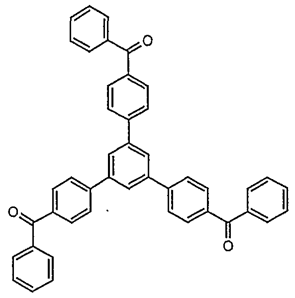
I. Stufe:I. level:
Eine Suspension von 135.8 g (250 mmol) 1 ,3,5-Tris(4'-bromphenyl)benzol, 93.9 g (800 mmol) Zink(ll)cyanid und 1.6 g Zink (25 mmol) in 2000 ml N,N-Dimethylacetamid wurde unter gutem Rühren mit 2.9 g (2.5 mmol) Tetrakis(triphenylphosphin)palladium(0) versetzt und 16 h bei 100 °C gerührt. Die Reaktionsmischung wurde nach Erkalten mit 2000 ml konz. wäßrigem Ammoniak versetzt. Der farblose Niederschlag wurde abgesaugt, fünfmal mit je 500 ml konz. wäßrigem Ammoniak, dreimal mit je 500 ml Wasser und dreimal mit je 300 ml Ethanol gewaschen. Anschließend wurde er in 2000 ml Ethanol suspendiert und unter Rückfluß ausgerührt. Nach Erkalten der Suspension wurde der Niederschlag abgesaugt und im Vakuum getrocknet. Ausbeute: 84.3 g (221 mmol), entsprechend 88.4 % d. Th., Reinheit 98% (nach NMR). 1H-NMR (CDCI3): δ [ppm] = 8.14 (s, 3H), 7.84 (d, 6H), 7.61 (d, 6H).A suspension of 135.8 g (250 mmol) 1, 3,5-tris (4'-bromophenyl) benzene, 93.9 g (800 mmol) zinc (II) cyanide and 1.6 g zinc (25 mmol) in 2000 ml N, N- Dimethylacetamide was mixed with good stirring with 2.9 g (2.5 mmol) of tetrakis (triphenylphosphine) palladium (0) and stirred at 100 ° C. for 16 h. After cooling, the reaction mixture was concentrated with 2000 ml. aqueous ammonia added. The colorless precipitate was filtered off, five times with 500 ml of conc. aqueous ammonia, washed three times with 500 ml of water and three times with 300 ml of ethanol. Then it was suspended in 2000 ml of ethanol and stirred under reflux. After the suspension had cooled, the precipitate was filtered off with suction and dried in vacuo. Yield: 84.3 g (221 mmol), corresponding to 88.4% of theory. Th., Purity 98% (according to NMR). 1 H NMR (CDCI 3 ): δ [ppm] = 8.14 (s, 3H), 7.84 (d, 6H), 7.61 (d, 6H).
2. Stufe:2nd stage:
Eine Suspension von 38.1 g (100 mmol) 1 ,3,5-Tris(4'-cyanophenyI)benzoI in 800 ml THF wurde bei Raumtemperatur während 15 min. mit 330 ml einer Phenylmagnesiumbromid-Lösung (1.0 molar in THF) versetzt. Anschließend wurde noch 30 min. bei Raumtemperatur und 5 h unter Rückfluß gerührt. Nach Erkalten wurden 100 ml 5 N HCI und 100 ml Ethanol zugegeben und erneut 16 h unter Rückfluß erhitzt. Nach Erkalten wurde die wäßrige Phase abgetrennt, die organische Phase wurde zur Trockene eingeengt. Der Rückstand wurde in 1000 ml Dichlormethan aufgenommen und fünfmal mit je 500 ml Wasser gewaschen. Nach Trocknen über Magnesiumsulfat wurde die organische Phase zur Trockene eingeengt. Der Rückstand wurde siebenmal aus DMSO (ca. 3 ml/g) umkristallisiert. Die Sublimation erfolgte bei T = 235 °C, p = 5 x 10"5 mbar im statischen Vakuum. Tm = 199 °C, Tg = 80 °C. Die Ausbeute an 1 ,3,5-Tris(1'-(4'-benzoyl)phenyl)benzol betrug 32.4 g (52 mmol), entsprechend 52.3 % d. Th., bei einer Reinheit vonA suspension of 38.1 g (100 mmol) 1, 3,5-tris (4'-cyanophenyI) benzoI in 800 ml THF was at room temperature for 15 min. 330 ml of a phenylmagnesium bromide solution (1.0 molar in THF) were added. Then 30 minutes. at room temperature and 5 h under reflux. After cooling, 100 ml of 5N HCl and 100 ml of ethanol were added and the mixture was heated under reflux again for 16 h. After cooling, the aqueous phase was separated off, the organic phase was evaporated to dryness. The residue was taken up in 1000 ml of dichloromethane and washed five times with 500 ml of water each. After drying over magnesium sulfate, the organic phase was evaporated to dryness. The residue was recrystallized seven times from DMSO (approx. 3 ml / g). The sublimation was carried out at T = 235 ° C, p = 5 x 10 "5 mbar in a static vacuum. T m = 199 ° C, T g = 80 ° C. The yield of 1, 3,5-tris (1'- (4'-benzoyl) phenyl) benzene was 32.4 g (52 mmol), corresponding to 52.3% of theory. Th., With a purity of
> 99.9 % (nach HPLC).> 99.9% (according to HPLC).
1H-NMR (CDCI3): δ [ppm] = 7.96 (d, 6H), 7.94 (s, 3H), 7.87 (d, 6H), 7.83 (d, 6H), 1 H-NMR (CDCI 3 ): δ [ppm] = 7.96 (d, 6H), 7.94 (s, 3H), 7.87 (d, 6H), 7.83 (d, 6H),
7.62 (dd, 3H), 7.51 (dd, 6H).7.62 (dd, 3H), 7.51 (dd, 6H).
Die Absorptionskante von E1 liegt bei 351 nm. Die Bestimmung derThe absorption edge of E1 is 351 nm. The determination of the
Absorptionskante wird in Fig. 1 gezeigt.Absorption edge is shown in Fig. 1.
Synthese-Beispiel 2: 1,3,5-Tris[(3'-benzoyI)benzoyI]benzoI (Elektronentransportmaterial E2)Synthesis example 2: 1,3,5-tris [(3'-benzoyI) benzoyI] benzoI (electron transport material E2)
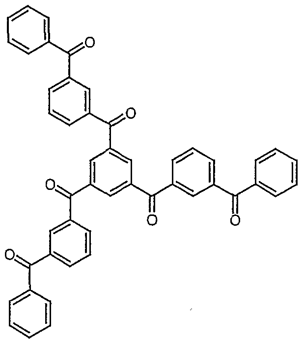
20.0 g 1 ,3,5-Tris[(3'-benzoyl)benzoyl]benzol, erhalten nach der Vorschrift von K. Matsuda et al. (s. o.), mit einer Reinheit von ca. 95 % wurden in 500 ml Dichlormethan gelöst und mit 500 ml einer 0.5 molaren wäßrigen Lösung von EDTA- Tetranatriumsalz 24 h intensiv gerührt, um Cr(lll)-Spuren zu entfernen. Die organische Phase wurde abgetrennt und fünfmal mit 300 ml destilliertem Wasser gewaschen. Nach Trocknen über Magnesiumsulfat wurde die organische Phase eingeengt und anschließend an Kieselgel chromatographiert (Laufmittel Dichlormethan : π-Hexan, 3:1). Die Sublimation erfolgte bei T = 330 °C, p = 5 x 10~5 mbar im statischen Vakuum. Tm und Tg konnten bei der glasartig angefallenen Verbindung nicht bestimmt werden. Die Ausbeute betrug 14.3 g, bei einer Reinheit von > 99.9 % (nach HPLC). Die Absorptionskante von E2 liegt bei 291 nm. Synthese-Beispiel 3: Elektronentransportmaterial E320.0 g 1, 3,5-tris [(3'-benzoyl) benzoyl] benzene, obtained according to the instructions from K. Matsuda et al. (see above), with a purity of approx. 95%, were dissolved in 500 ml dichloromethane and stirred intensively with 500 ml of a 0.5 molar aqueous solution of EDTA tetrasodium salt for 24 hours in order to remove traces of Cr (III). The organic phase was separated and washed five times with 300 ml of distilled water. After drying over magnesium sulfate, the organic phase was concentrated and then chromatographed on silica gel (mobile phase dichloromethane: π-hexane, 3: 1). The sublimation was carried out at T = 330 ° C, p = 5 x 10 ~ 5 mbar in a static vacuum. T m and T g could not be determined for the glassy compound. The yield was 14.3 g, with a purity of> 99.9% (according to HPLC). The absorption edge of E2 is 291 nm. Synthesis example 3: electron transport material E3

I. Stufe:I. level:
Eine auf -78 °C gekühlte Mischung von 123.6 g (500 mmol) 2-Bromphenyl- phenyl)methan in 2000 ml THF wurde unter gutem Rühren tropfenweise mit 200 ml (500 mmol) t?-BuLi (2.5 molare Lösung in π-Hexan) versetzt und 15 min. gerührt. Diese Lösung wurde während 15 min. zu einer gut gerührten, auf -10 °C gekühlten Suspension von 169.0 g (500 mmol) 2,7-Dibromfluorenon geschlaucht. Nach Erwärmen der Reaktionsmischung auf Raumtemperatur wurde diese im Vakuum zur Trockene eingeengt. Der honigartige Rückstand wurde in 2000 ml Eisessig suspendiert, mit 10 ml konz. Salzsäure versetzt und 5 h unter Rückfluß erhitzt. Der ausgefallene Feststoff wurde aus der warmen Reaktionsmischung (80 °C) abfiltriert und mit 200 ml Eisessig gewaschen. Der Feststoff wurde erneut aus 1000 ml Eisessig umkristallisiert. Ausbeute: 198.7 g (407 mmol), entsprechend 81.4 % d. Th., Reinheit 97 % (nach NMR).A mixture of 123.6 g (500 mmol) 2-bromophenylphenyl) methane in 2000 ml THF, cooled to -78 ° C, was added dropwise with 200 ml (500 mmol) t? -BuLi (2.5 molar solution in π-hexane) while stirring well ) added and 15 min. touched. This solution was kept for 15 min. to a well-stirred suspension of 169.0 g (500 mmol) of 2,7-dibromofluorenone, cooled to -10 ° C. After the reaction mixture had been warmed to room temperature, it was evaporated to dryness in vacuo. The honey-like residue was suspended in 2000 ml of glacial acetic acid, with 10 ml of conc. Hydrochloric acid added and heated under reflux for 5 h. The precipitated solid was filtered off from the warm reaction mixture (80 ° C.) and washed with 200 ml of glacial acetic acid. The solid was recrystallized again from 1000 ml of glacial acetic acid. Yield: 198.7 g (407 mmol), corresponding to 81.4% of theory. Th., Purity 97% (according to NMR).
1H-NMR (CDCI3): D [ppm] = 7.63 (d, 2H), 7.47 (dd, 2H), 7.39 (br. d, 2H), 7.21 (dd, 2H), 7.11 (d, 2H), 6.96 (dd, 2H), 6.42 (br. d, 2H), 4.48 (s, 2H). 1 H-NMR (CDCI 3 ): D [ppm] = 7.63 (d, 2H), 7.47 (dd, 2H), 7.39 (br. D, 2H), 7.21 (dd, 2H), 7.11 (d, 2H) , 6.96 (dd, 2H), 6.42 (br. D, 2H), 4.48 (s, 2H).
2. Stufe:2nd stage:
Eine Suspension von 195.3 g (400 mmol) des Produkts der 1. Stufe und 238.4 g (800 mmol) Natriumdichromat-dihydrat in 2000 ml Eisessig wurde unter gutem Rühren langsam zum Sieden erhitzt und 6 h unter Rückfluß gekocht. Nach Erkalten wurde der feinkristalline Niederschlag abgesaugt, zweimal mit je 200 ml Eisessig, zehnmal mit je 200 ml warmem Wasser, dann dreimal mit je 200 ml Ethanol gewaschen und im Vakuum getrocknet. Das so erhaltene Rohprodukt wurde zweimal aus Chlorbenzol (ca. 4 ml/g) umkristallisiert. Ausbeute: 154.6 g (308 mmol), entsprechend 77.0 % d. Th., Reinheit 99.5 % (nach NMR). 1H-NMR (CDCI3): D [ppm] = 8.45 (d, 2H), 7.69 (d, 2H), 7.52 (d, 2H), 7.44 (dd, 2H), 7.32 (dd, 2H), 6.97 (s, 2H), 6.53 (d, 2H).A suspension of 195.3 g (400 mmol) of the product of the 1st stage and 238.4 g (800 mmol) of sodium dichromate dihydrate in 2000 ml of glacial acetic acid was slowly heated to boiling with good stirring and boiled under reflux for 6 h. After cooling, the finely crystalline precipitate was filtered off, washed twice with 200 ml of glacial acetic acid, ten times with 200 ml of warm water, then three times with 200 ml of ethanol and dried in vacuo. The crude product thus obtained was recrystallized twice from chlorobenzene (approx. 4 ml / g). Yield: 154.6 g (308 mmol), corresponding to 77.0% of theory. Th., Purity 99.5% (according to NMR). 1 H-NMR (CDCI3): D [ppm] = 8.45 (d, 2H), 7.69 (d, 2H), 7.52 (d, 2H), 7.44 (dd, 2H), 7.32 (dd, 2H), 6.97 ( s, 2H), 6.53 (d, 2H).
3. Stufe:3rd stage:
Eine gut gerührte Suspension von 37.7 g (75 mmol) des Produkts der 2. Stufe, 55.8 g (300 mmol) 4-Methyl-naphtalin-1-boronsäure, 78.2 g (315 mmol) Kaluimphosphat-monohydrat in einem Gemisch aus 100 ml Dioxan, 250 ml Toluol und 300 ml Wasser wurde mit 1.37 g (4.5 mmol) Tri-o-tolylphosphin und dann mit 168 mg (0.75 mol) Palladium(ll)acetat versetzt und 16 h unter Rückfluß erhitzt. Nach Erkalten der Reaktionsmischung wurde der ausgefallene Feststoff abgesaugt, mit je 100 ml Wasser und Ethanol gewaschen und getrocknet. Der Feststoff wurde in einen Soxhlett-Extraktor plaziert und mit Chloroform durch eine Glasfaserextraktionshülse (Porengröße 0.1 μm) extrahiert. Das Chloroform wurde auf ein Volumen von 100 ml eingeengt und mit 500 ml Ethanol versetzt. Der resultierende Niederschlag wurde abgesaugt und mit Ethanol gewaschen. Anschließend wurde der Feststoff viermal aus DMF (ca. 6 ml/g) umkristallisiert. Die Sublimation erfolgte bei T = 345 °C, p = 5 x 10"5 mbar im statischen Vakuum. Tm = 329 °C, Tg = 139 °C. Die Ausbeute des Elektronentransportmaterials E3 betrug 36.9 g (59 mmol), entsprechend 78.7 % d. Th., bei einer Reinheit von > 99.9 % (nach HPLC).A well-stirred suspension of 37.7 g (75 mmol) of the product of the second stage, 55.8 g (300 mmol) of 4-methyl-naphthalene-1-boronic acid, 78.2 g (315 mmol) Potassium phosphate monohydrate in a mixture of 100 ml of dioxane, 250 ml of toluene and 300 ml of water was mixed with 1.37 g (4.5 mmol) of tri-o-tolylphosphine and then with 168 mg (0.75 mol) of palladium (II) acetate and added for 16 hours Heated to reflux. After the reaction mixture had cooled, the precipitated solid was filtered off with suction, washed with 100 ml of water and ethanol each time and dried. The solid was placed in a Soxhlett extractor and extracted with chloroform through a glass fiber extraction thimble (pore size 0.1 μm). The chloroform was concentrated to a volume of 100 ml and 500 ml of ethanol were added. The resulting precipitate was filtered off and washed with ethanol. The solid was then recrystallized four times from DMF (approx. 6 ml / g). The sublimation was carried out at T = 345 ° C, p = 5 x 10 "5 mbar in a static vacuum. Tm = 329 ° C, T g = 139 ° C. The yield of the electron transport material E3 was 36.9 g (59 mmol), corresponding to 78.7 % of theory, with a purity of> 99.9% (according to HPLC).
1H-NMR (TCE-d2): D [ppm] = 8.34 (m, 2H), 8.06 (d, 2H), 8.00 (d, 2H), 7.71 (d, 2H), 7.61 (d, 2H), 7.49 (dd, 2H), 7.41 (m, 4H), 7.32 (d, 2H), 7.25 (d, 2H), 7.23 (d, 2H), 7.02 (s, 2H), 6.87 (m, 2H), 2.68 (s, 6H). Die Absorptionskante von E3 liegt bei 383 nm. 1 H-NMR (TCE-d2): D [ppm] = 8.34 (m, 2H), 8.06 (d, 2H), 8.00 (d, 2H), 7.71 (d, 2H), 7.61 (d, 2H), 7.49 (dd, 2H), 7.41 (m, 4H), 7.32 (d, 2H), 7.25 (d, 2H), 7.23 (d, 2H), 7.02 (s, 2H), 6.87 (m, 2H), 2.68 (s, 6H). The absorption edge of E3 is 383 nm.
Synthese-Beispiel 4: Bis[4-(4'-methyl-naphth-1 '-yl)-naphth-1 -yl)ketonSynthesis Example 4: Bis [4- (4'-methyl-naphth-1'-yl) -naphth-1-yl) ketone
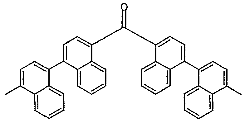
I . Stufe:I. Step:
Eine gut gerührte Suspension von 93.0 g (500 mmol) 4-Methylnaphtalin-1- boronsäure, 76.5 ml (550 mmol) 1 -Bromnaphthalin, 245.2 g (1155 mmol) Trikaliumphosphat-monohydrat in einem Gemisch aus 500 ml Dioxan, 750 ml Toluol und 1250 ml Wasser wurde mit 1.83 g (6 mmol) o-Tolylphosphin und dann mit 225 mg (1 mmol) Palladium(ll)acetat versetzt. Nach 16 h Kochen unter Rückfluß und anschließendem Erkalten wurde die organische Phase abgetrennt, über Kieselgel filtriert und zur Trockene eingeengt. Der Rückstand wurde einmal mit 500 ml Ethanol ausgerührt. Ausbeute: 126.0 g (470 mmol), entsprechend 93.9 % d. Th., Reinheit 97 % (nach NMR).A well-stirred suspension of 93.0 g (500 mmol) of 4-methylnaphtalin-1-boronic acid, 76.5 ml (550 mmol) of 1-bromonaphthalene, 245.2 g (1155 mmol) of tripotassium phosphate monohydrate in a mixture of 500 ml of dioxane, 750 ml of toluene and 1250 ml of water were mixed with 1.83 g (6 mmol) of o-tolylphosphine and then with 225 mg (1 mmol) of palladium (II) acetate. After boiling under reflux for 16 h and then cooling, the organic phase was separated off, filtered through silica gel and evaporated to dryness. The residue was stirred once with 500 ml of ethanol. Yield: 126.0 g (470 mmol), corresponding to 93.9% of theory. Th., Purity 97% (according to NMR).
1H-NMR (CDCI3): δ [ppm] = 8.09 (d, 1 H), 7.93(d, 2H), 7.59-7.39 (m, 8H), 7.30-7.25 (m, 2H), 2.80 (s, 3H). 2. Stufe: 1 H-NMR (CDCI 3 ): δ [ppm] = 8.09 (d, 1 H), 7.93 (d, 2H), 7.59-7.39 (m, 8H), 7.30-7.25 (m, 2H), 2.80 (see , 3H). 2nd stage:
Eine auf 0 °C gekühlte, lichtgeschützte Lösung von 126.0 g (470 mmol) 1-(4'-Methylnaphth-1'-yl)-naphthalin in 1000 ml Chloroform wurde tropfenweise mit einem Gemisch aus 26.5 ml (517 mmol) Brom und 500 ml Chloroform versetzt. Nach vollendeter Zugabe wurde noch 14 h bei Raumtemperatur gerührt. Die organische Phase wurde mit 1000 ml wäßriger gesättigter Natriumsulfit-Lösung und anschließend dreimal mit je 300 ml Wasser gewaschen. Nach Trocknen über Magnesiumsulfat und Einengen wurde der wachsartige Feststoff zweimal in 500 ml Ethanol am Rückfluß ausgerührt. Ausbeute: 123.3 g (355 mmol) entsprechend 75.5 % d. Th., Reinheit 98 % (nach NMR).A light-protected solution of 126.0 g (470 mmol) of 1- (4'-methylnaphth-1'-yl) -naphthalene in 1000 ml of chloroform, cooled to 0 ° C., was added dropwise with a mixture of 26.5 ml (517 mmol) of bromine and 500 ml of chloroform are added. After the addition was complete, the mixture was stirred at room temperature for a further 14 h. The organic phase was washed with 1000 ml of aqueous saturated sodium sulfite solution and then three times with 300 ml of water. After drying over magnesium sulfate and concentration, the waxy solid was stirred twice in 500 ml of ethanol under reflux. Yield: 123.3 g (355 mmol) corresponding to 75.5% of theory. Th., Purity 98% (according to NMR).
1H-NMR (CDCIs): δ [ppm] = 8.35 (d, 1 H), 8.10 (d, 1 H), 7.88 (d, 1 H), 7.58 (dd, 1 H), 7.51 (dd, 1 H), 7.44-7.28 (m, 7H), 2.80 (s, 3H). 1 H-NMR (CDCIs): δ [ppm] = 8.35 (d, 1 H), 8.10 (d, 1 H), 7.88 (d, 1 H), 7.58 (dd, 1 H), 7.51 (dd, 1 H), 7.44-7.28 (m, 7H), 2.80 (s, 3H).
3. Stufe:3rd stage:
Eine gut gerührte, auf -78 °C gekühlte Suspension von 69.5 g (200 mmol) 4-Brom- 1-(4-methylnaphth-1-yl)naphthalin in 1000 ml THF wurde tropfenweise mit 80 ml (200 mmol) π-BuLi (2.5 molare Lösung in π-Hexan) versetzt und 2 h gerührt. Diese Suspension wurde tropfenweise mit einem Gemisch aus 9.2 ml (100 mmol) N,N-DimethyI-carbamidsäurechlorid und 100 ml THF versetzt. Anschließend wurde 1 h bei -78 °C gerührt. Nach Erwärmen auf Raumtemperatur wurde die Mischung mit 10 ml Essigsäure und 50 ml Wasser versetzt und zur Trockene eingeengt. Der ölige Rückstand wurde in 100 ml siedendem Aceton gelöst und langsam unter Rückfluß mit 500 ml Essigsäure versetzt. Nach Erkalten und Absaugen wurde das Rohprodukt noch zweimal aus Aceton / Essigsäure und siebenmal aus DMSO (ca. 3 ml/g) umkristallisiert. Die Sublimation erfolgte bei T = 340 °C, p = 5 x 10"5 mbar im statischen Vakuum. Tm= 336 °C, Tg = 133 °C. Die Ausbeute an Bis[4-(4'-methyl- naphth-1'-yl)-naphth-1-yl)keton betrug 35.5 g (63 mmol), entsprechend 63.1 % d. Th., bei einer Reinheit von > 99.9 % (nach HPLC).A well-stirred suspension of 69.5 g (200 mmol) of 4-bromo-1- (4-methylnaphth-1-yl) naphthalene in 1000 ml of THF, cooled to -78 ° C., was added dropwise with 80 ml (200 mmol) of π-BuLi (2.5 molar solution in π-hexane) and stirred for 2 h. A mixture of 9.2 ml (100 mmol) of N, N-dimethyI-carbamic acid chloride and 100 ml of THF was added dropwise to this suspension. The mixture was then stirred at -78 ° C for 1 h. After warming to room temperature, 10 ml of acetic acid and 50 ml of water were added and the mixture was concentrated to dryness. The oily residue was dissolved in 100 ml of boiling acetone and slowly treated with 500 ml of acetic acid under reflux. After cooling and suction filtration, the crude product was recrystallized twice from acetone / acetic acid and seven times from DMSO (approx. 3 ml / g). The sublimation was carried out at T = 340 ° C, p = 5 x 10 "5 mbar in a static vacuum. T m = 336 ° C, T g = 133 ° C. The yield of bis [4- (4'-methyl-naphth -1'-yl) -naphth-1-yl) ketone was 35.5 g (63 mmol), corresponding to 63.1% of theory, with a purity of> 99.9% (according to HPLC).
1H-NMR (CDCI3): δ [ppm] = 8.79 (d, 2H), 8.14 (d, 2H), 7.86 (d, 2H), 7,64-7,34 (m, 18H), 2.84 (s, 6H). Die Absorptionskante von E4 liegt bei 396 nm. 1 H NMR (CDCI 3 ): δ [ppm] = 8.79 (d, 2H), 8.14 (d, 2H), 7.86 (d, 2H), 7.64-7.34 (m, 18H), 2.84 ( s, 6H). The absorption edge of E4 is 396 nm.
Herstellung der organischen Elektrolumineszenzvorrichtungen:Manufacture of organic electroluminescent devices:
Die Herstellung von OLEDs erfolgte nach einem allgemeinen Verfahren gemäß WO 04/058911 , das im Einzelfall auf die jeweiligen Gegebenheiten (z. B. Schichtdickenvariation, um optimale Effizienz bzw. Farbe zu erreichen) angepaßt werden mußte. In den folgenden Beispielen werden die Ergebnisse verschiedener OLEDs vorgestellt. Der grundlegende Aufbau, die verwendeten Materialien und Schichtdicken, außer der Elektronentransportschicht, waren zur besseren Vergleichbarkeit identisch. Analog dem o. g. allgemeinen Verfahren wurden OLEDs mit folgendem Aufbau erzeugt: Lochinjektionsschicht (HIL) 60 nm PEDOT (aus Wasser aufgeschleudert; bezogen von H. C. Starck; Poly(3,4-ethylendioxy-2,5-thiophen) Lochtransportschicht (HTM) 20 nm NaphDATA (aufgedampft; bezogen von SynTec; 4,4',4"-Tris(N-1 -naphthyl-N-phenyl-amino)- triphenylamin Lochtransportschicht (HTM) 20 nm S-TAD (aufgedampft; hergestellt nach WO 99/12888; 2,2',7,7'-Tetrakis(diphenylamino)-spiro- 9,9'-bifluoren) Emissionschicht (EML) Spiro-DPVBi (hergestellt nach WO 02/10093, 2,2',7,7'- Tetrakis(2,2'-diphenylvinyl)-spiro-9,9'-bifluoren) dotiert mit 1 % S-TAD (2,2',7,7'-Tetrakis(diphenylamino)- spiro-9,9'-bifluoren) Elektronenleiter (ETL) 10 nm - 50 nm (genauer Aufbau siehe Beispiele in Tabelle 1) (aufgedampft: AIQ3 bezogen von SynTec; Tris(chinolinato)aluminium(III) oder die Elektronentransportmaterialien E1 bis E4 Ba-Al (Kathode) 3 nm Ba, darauf 150 nm AI.OLEDs were produced by a general process according to WO 04/058911, which had to be adapted to the particular circumstances in each individual case (e.g. layer thickness variation in order to achieve optimum efficiency or color). The results of various OLEDs are presented in the following examples. The basic structure, the materials and layer thicknesses used, apart from the electron transport layer, were identical for better comparability. OLEDs with the following structure were produced analogously to the above-mentioned process: Hole injection layer (HIL) 60 nm PEDOT (spun on from water; obtained from HC Starck; poly (3,4-ethylenedioxy-2,5-thiophene) hole transport layer (HTM) 20 nm NaphDATA (evaporated; obtained from SynTec; 4,4 ', 4 "tris (N-1-naphthyl-N-phenylamino) triphenylamine hole transport layer (HTM) 20 nm S-TAD (evaporated; produced according to WO 99/12888; 2,2 ', 7,7'-tetrakis (diphenylamino) -spiro- 9,9'-bifluorene) emission layer (EML) Spiro-DPVBi (manufactured according to WO 02/10093, 2,2', 7,7'-tetrakis (2,2'-diphenylvinyl) -spiro-9,9'-bifluorene) doped with 1% S-TAD (2,2 ', 7,7'-tetrakis (diphenylamino) - spiro-9,9'-bifluorene) Electron conductor (ETL) 10 nm - 50 nm (for exact structure see examples in Table 1) (evaporated: AIQ 3 obtained from SynTec; Tris (quinolinato) aluminum (III) or the electron transport materials E1 to E4 Ba-Al (cathode) 3 nm Ba , then 150 nm AI.
Diese noch nicht optimierten OLEDs wurden standardmäßig charakterisiert; hierfür wurden die Elektrolumineszenzspektren, die Effizienz (gemessen in cd/A), die Leistungseffizienz (gemessen in Im/W) in Abhängigkeit der Helligkeit, berechnet aus Strom-Spannungs-Helligkeit-Kennlinien (lUL-Kennlinien), und die Lebensdauer bestimmt. Als Lebensdauer wird die Zeit definiert, nach der die Anfangshelligkeit der OLED bei einer konstanten Stromdichte von 10 mA/cm2 auf die Hälfte gesunken ist. Für die Elektronentransportschicht wurde für jedes Material separat die Schichtdicke optimiert. Zum besseren Vergleich sind jedoch auch die dickeren AIQ3- Schichtdicken mit aufgeführt, die direkt mit den Schichtdicken von E1 und E2 vergleichbar sind.These OLEDs, which have not yet been optimized, have been characterized as standard; For this purpose, the electroluminescence spectra, the efficiency (measured in cd / A), the power efficiency (measured in Im / W) depending on the brightness, calculated from current-voltage-brightness characteristics (IUL characteristics), and the service life were determined. The lifetime is defined as the time after which the initial brightness of the OLED has halved at a constant current density of 10 mA / cm 2 . The layer thickness was optimized separately for each material for the electron transport layer. For a better comparison, however, the thicker AIQ 3 layer thicknesses are also listed, which are directly comparable with the layer thicknesses of E1 and E2.
In Tabelle 1 sind die Ergebnisse einiger Beispiele zusammengefaßt, wobei jeweils die Zusammensetzung der ETL inklusive der Schichtdicken mit aufgeführt ist. Die ETLs enthalten beispielsweise als Elektronentransportmaterial die Verbindungen E1 bis E4. Als Vergleichsbeispiele dienen OLEDs, die gemäß dem Stand der Technik als Elektronenleiter AIQ3 enthalten.The results of some examples are summarized in Table 1, the composition of the ETL including the layer thicknesses being listed in each case. For example, the ETLs contain the compounds E1 as electron transport material to E4. OLEDs which contain AIQ 3 as the electron conductor according to the prior art serve as comparative examples.
Zur besseren Übersichtlichkeit sind die Strukturformeln der verwendeten Substanzen im folgenden dargestellt.The structural formulas of the substances used are shown below for better clarity.

Tabelle 1 :Table 1 :
M MM M
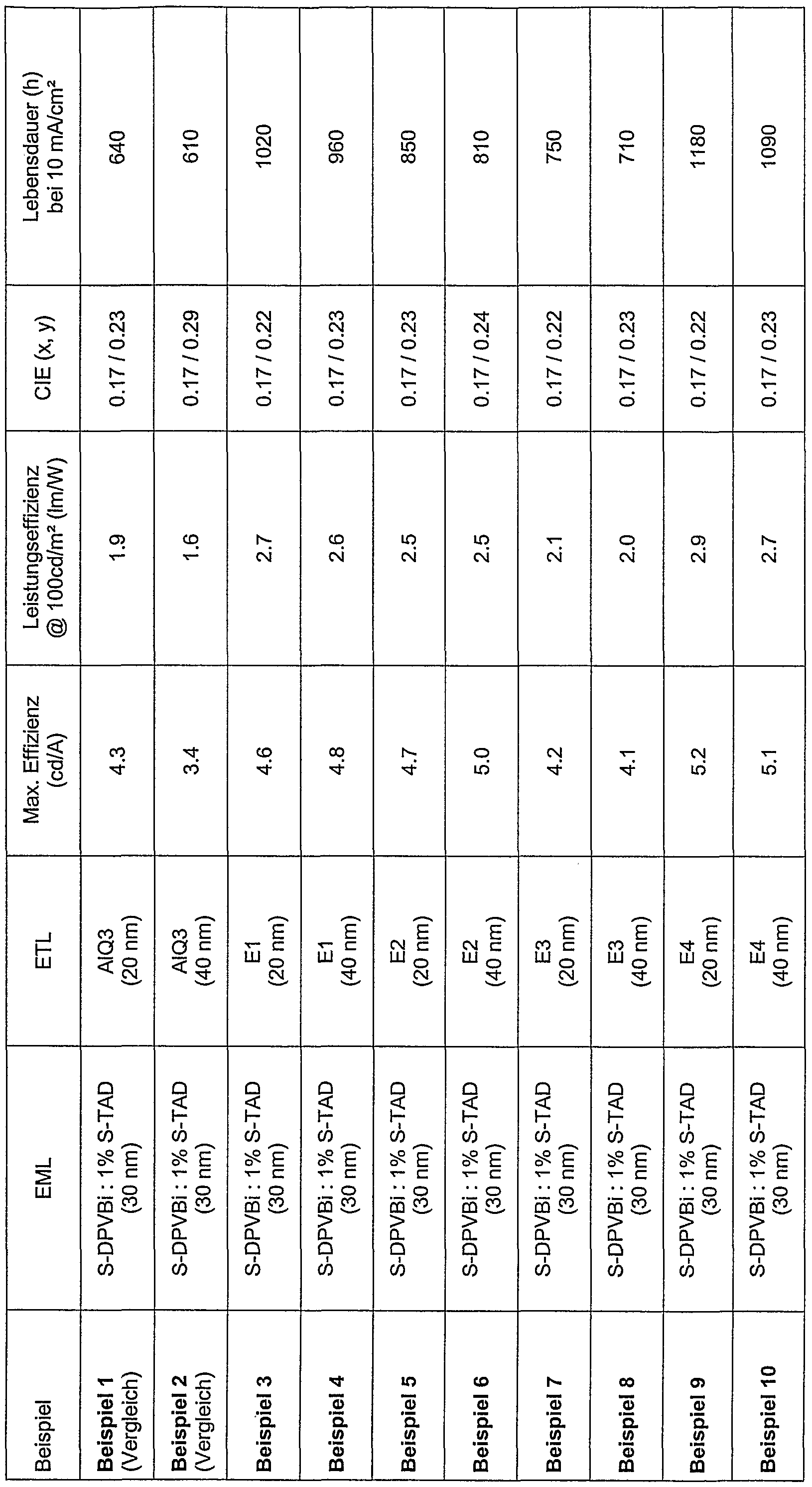
Alle OLEDs zeigen blaue Emission, die vom Fluoreszenzemitter S-DPVBi stammt. Man erhält höhere photometrische Effizienzen in Devices, bei denen der Elektronenleiter AIQ3 durch die erfindungsgemäßen Elektronenleiter E1 bis E4 ersetzt wurde. Da hier auch die Spannungen, die man zur Erreichung einer bestimmten Helligkeit benötigt, niedrig sind, erhält man eine sehr gute Leistungseffizienz. Die Lebensdauer steigt von ca. 650 h auf bis zu über 1100 h an. Insbesondere sind bei gleicher Schichtdicke der ETL die Effizienzen, die Leistungseffizienzen, die Lebensdauer und die Farbe mit den erfindungsgemäßen Elektronentransportmaterialien besser als mit dem Standard-Elektronenleiter AIQ3.All OLEDs show blue emission, which comes from the fluorescence emitter S-DPVBi. Higher photometric efficiencies are obtained in devices in which the AIQ 3 electron conductor has been replaced by the electron conductors E1 to E4 according to the invention. Since the voltages required to achieve a certain brightness are also low here, very good power efficiency is obtained. The service life increases from approx. 650 h to over 1100 h. In particular, with the same layer thickness of the ETL, the efficiencies, the power efficiencies, the service life and the color are better with the electron transport materials according to the invention than with the standard electron conductor AIQ 3 .
Zusammenfassend kann gesagt werden, daß OLEDs, gefertigt nach dem neuen Designprinzip, eine höhere Effizienz bei niedrigeren Spannungen und längerer Lebensdauer aufweisen, wie man leicht Tabelle 1 entnehmen kann. In summary, it can be said that OLEDs, manufactured according to the new design principle, have a higher efficiency at lower voltages and a longer service life, as can easily be seen in Table 1.
Claims
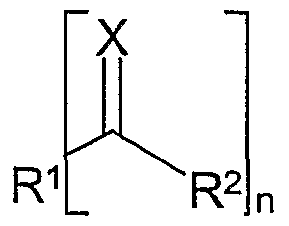

Priority Applications (5)
| Application Number | Priority Date | Filing Date | Title |
|---|---|---|---|
| US10/589,847 US7838126B2 (en) | 2004-02-20 | 2005-02-18 | Organic electronic devices |
| JP2006553551A JP5253739B2 (en) | 2004-02-20 | 2005-02-18 | Organic electronic devices |
| EP05707510A EP1716724A1 (en) | 2004-02-20 | 2005-02-18 | Organic electronic devices |
| US10/590,037 US7776455B2 (en) | 2004-02-20 | 2005-02-18 | Organic electronic devices |
| KR1020067016687A KR101175959B1 (en) | 2004-02-20 | 2006-08-18 | Organic electronic devices |
Applications Claiming Priority (2)
| Application Number | Priority Date | Filing Date | Title |
|---|---|---|---|
| DE102004008304.5 | 2004-02-20 | ||
| DE102004008304A DE102004008304A1 (en) | 2004-02-20 | 2004-02-20 | Organic electronic devices |
Publications (1)
| Publication Number | Publication Date |
|---|---|
| WO2005084081A1 true WO2005084081A1 (en) | 2005-09-09 |
Family
ID=34832853
Family Applications (2)
| Application Number | Title | Priority Date | Filing Date |
|---|---|---|---|
| PCT/EP2005/001710 Ceased WO2005084082A1 (en) | 2004-02-20 | 2005-02-18 | Organic electronic devices |
| PCT/EP2005/001709 Ceased WO2005084081A1 (en) | 2004-02-20 | 2005-02-18 | Organic electronic devices |
Family Applications Before (1)
| Application Number | Title | Priority Date | Filing Date |
|---|---|---|---|
| PCT/EP2005/001710 Ceased WO2005084082A1 (en) | 2004-02-20 | 2005-02-18 | Organic electronic devices |
Country Status (7)
| Country | Link |
|---|---|
| US (2) | US7838126B2 (en) |
| EP (2) | EP1716725A1 (en) |
| JP (2) | JP2007527116A (en) |
| KR (2) | KR20060127138A (en) |
| CN (2) | CN100482023C (en) |
| DE (1) | DE102004008304A1 (en) |
| WO (2) | WO2005084082A1 (en) |
Cited By (236)
| Publication number | Priority date | Publication date | Assignee | Title |
|---|---|---|---|---|
| WO2007022845A1 (en) | 2005-08-26 | 2007-03-01 | Merck Patent Gmbh | Novel materials for organic electroluminescent devices |
| JP2007129206A (en) * | 2005-10-04 | 2007-05-24 | Fujifilm Corp | Organic electroluminescence device |
| WO2008006449A1 (en) | 2006-07-11 | 2008-01-17 | Merck Patent Gmbh | Novel materials for organic electroluminescent devices |
| WO2008142921A1 (en) * | 2007-05-24 | 2008-11-27 | Nitto Denko Corporation | Optical film, display, diethynylfluorene and polymer thereof |
| DE102007024850A1 (en) | 2007-05-29 | 2008-12-04 | Merck Patent Gmbh | New materials for organic electroluminescent devices |
| JP2009001769A (en) * | 2007-05-24 | 2009-01-08 | Nitto Denko Corp | Optical film, image display device, diethynylfluorene and polymer thereof |
| DE102008018670A1 (en) | 2008-04-14 | 2009-10-15 | Merck Patent Gmbh | New materials for organic electroluminescent devices |
| DE102008035413A1 (en) | 2008-07-29 | 2010-02-04 | Merck Patent Gmbh | Connections for organic electronic devices |
| WO2010049050A1 (en) | 2008-10-31 | 2010-05-06 | Merck Patent Gmbh | Novel materials for organic electroluminescence devices |
| DE102008063490A1 (en) | 2008-12-17 | 2010-06-24 | Merck Patent Gmbh | Organic electroluminescent device |
| DE102009005290A1 (en) | 2009-01-20 | 2010-07-22 | Merck Patent Gmbh | Connections for electronic devices |
| DE102009005289A1 (en) | 2009-01-20 | 2010-07-22 | Merck Patent Gmbh | Materials for organic electroluminescent devices |
| DE102009005288A1 (en) | 2009-01-20 | 2010-07-22 | Merck Patent Gmbh | Materials for organic electroluminescent devices |
| DE102009005746A1 (en) | 2009-01-23 | 2010-07-29 | Merck Patent Gmbh | Materials for organic electroluminescent devices |
| DE102009009277A1 (en) | 2009-02-17 | 2010-08-19 | Merck Patent Gmbh | Organic electronic device |
| DE102009012346A1 (en) | 2009-03-09 | 2010-09-16 | Merck Patent Gmbh | Organic electroluminescent device |
| WO2010115498A1 (en) | 2009-04-09 | 2010-10-14 | Merck Patent Gmbh | Organic electroluminescence device |
| EP2248869A2 (en) | 2005-09-12 | 2010-11-10 | Merck Patent GmbH | Compounds for organic electronic devices |
| WO2010149259A2 (en) | 2009-06-22 | 2010-12-29 | Merck Patent Gmbh | Conducting formulation |
| WO2011006574A1 (en) | 2009-07-14 | 2011-01-20 | Merck Patent Gmbh | Materials for organic electroluminescent devices |
| DE102009034625A1 (en) | 2009-07-27 | 2011-02-03 | Merck Patent Gmbh | New materials for organic electroluminescent devices |
| WO2011015265A2 (en) | 2009-08-04 | 2011-02-10 | Merck Patent Gmbh | Electronic devices comprising multi cyclic hydrocarbons |
| DE102009041289A1 (en) | 2009-09-16 | 2011-03-17 | Merck Patent Gmbh | Organic electroluminescent device |
| WO2011032686A1 (en) | 2009-09-16 | 2011-03-24 | Merck Patent Gmbh | Formulas for producing electronic devices |
| DE102009042680A1 (en) | 2009-09-23 | 2011-03-24 | Merck Patent Gmbh | Organic electroluminescent device |
| WO2011035836A1 (en) | 2009-09-23 | 2011-03-31 | Merck Patent Gmbh | Materials for electronic devices |
| WO2011054442A2 (en) | 2009-11-06 | 2011-05-12 | Merck Patent Gmbh | Materials for electronic devices |
| DE102009052428A1 (en) | 2009-11-10 | 2011-05-12 | Merck Patent Gmbh | Connection for electronic devices |
| DE102009033371A1 (en) | 2009-07-16 | 2011-05-12 | Merck Patent Gmbh | Materials for electronic devices |
| WO2011076325A1 (en) | 2009-12-23 | 2011-06-30 | Merck Patent Gmbh | Compositions comprising polymeric binders |
| WO2011076323A1 (en) | 2009-12-22 | 2011-06-30 | Merck Patent Gmbh | Formulations comprising phase-separated functional materials |
| WO2011076324A1 (en) | 2009-12-23 | 2011-06-30 | Merck Patent Gmbh | Compositions comprising organic semiconducting compounds |
| WO2011076326A1 (en) | 2009-12-22 | 2011-06-30 | Merck Patent Gmbh | Electroluminescent functional surfactants |
| WO2011076314A1 (en) | 2009-12-22 | 2011-06-30 | Merck Patent Gmbh | Electroluminescent formulations |
| WO2011088877A1 (en) | 2010-01-25 | 2011-07-28 | Merck Patent Gmbh | Compounds for electronic devices |
| DE102010009193A1 (en) | 2010-02-24 | 2011-08-25 | Merck Patent GmbH, 64293 | Fluorine-fluorine associates |
| DE102010009903A1 (en) | 2010-03-02 | 2011-09-08 | Merck Patent Gmbh | Connections for electronic devices |
| DE102010010481A1 (en) | 2010-03-06 | 2011-09-08 | Merck Patent Gmbh | Organic electroluminescent device |
| WO2011110277A1 (en) | 2010-03-11 | 2011-09-15 | Merck Patent Gmbh | Fibers in therapy and cosmetics |
| DE102010010631A1 (en) | 2010-03-09 | 2011-09-15 | Merck Patent Gmbh | Materials for electronic devices |
| WO2011110275A2 (en) | 2010-03-11 | 2011-09-15 | Merck Patent Gmbh | Radiative fibers |
| WO2011116869A1 (en) | 2010-03-26 | 2011-09-29 | Merck Patent Gmbh | Compounds for electronic devices |
| WO2011128035A1 (en) | 2010-04-12 | 2011-10-20 | Merck Patent Gmbh | Composition and method for preparation of organic electronic devices |
| WO2011128034A1 (en) | 2010-04-12 | 2011-10-20 | Merck Patent Gmbh | Composition having improved performance |
| WO2011128017A1 (en) | 2010-04-14 | 2011-10-20 | Merck Patent Gmbh | Bridged triarylamines and -phosphines as materials for electronic devices |
| WO2011137922A1 (en) | 2010-05-03 | 2011-11-10 | Merck Patent Gmbh | Formulations and electronic devices |
| DE102010020044A1 (en) | 2010-05-11 | 2011-11-17 | Merck Patent Gmbh | Organic electroluminescent device |
| WO2011147523A1 (en) | 2010-05-27 | 2011-12-01 | Merck Patent Gmbh | Formulation and method for preparation of organic electronic devices |
| WO2011147522A1 (en) | 2010-05-27 | 2011-12-01 | Merck Patent Gmbh | Compositions comprising quantum dots |
| DE102010024542A1 (en) | 2010-06-22 | 2011-12-22 | Merck Patent Gmbh | Materials for electronic devices |
| DE102010024335A1 (en) | 2010-06-18 | 2011-12-22 | Merck Patent Gmbh | Connections for electronic devices |
| WO2012013272A1 (en) | 2010-07-26 | 2012-02-02 | Merck Patent Gmbh | Quantum dots and hosts |
| WO2012013270A1 (en) | 2010-07-26 | 2012-02-02 | Merck Patent Gmbh | Nanocrystals in devices |
| DE102010033548A1 (en) | 2010-08-05 | 2012-02-09 | Merck Patent Gmbh | Materials for electronic devices |
| DE102010048074A1 (en) | 2010-10-09 | 2012-04-12 | Merck Patent Gmbh | Materials for electronic devices |
| DE102010048607A1 (en) | 2010-10-15 | 2012-04-19 | Merck Patent Gmbh | Connections for electronic devices |
| WO2012048781A1 (en) | 2010-10-15 | 2012-04-19 | Merck Patent Gmbh | Triphenylene-based materials for organic electroluminescent devices |
| DE102010054316A1 (en) | 2010-12-13 | 2012-06-14 | Merck Patent Gmbh | Substituted tetraarylbenzenes |
| US8206839B2 (en) | 2005-10-04 | 2012-06-26 | Fujifilm Corporation | Organic electroluminescent element |
| WO2012084115A1 (en) | 2010-12-23 | 2012-06-28 | Merck Patent Gmbh | Organic electroluminescent device |
| WO2012095143A1 (en) | 2011-01-13 | 2012-07-19 | Merck Patent Gmbh | Compounds for organic electroluminescent devices |
| EP2482159A2 (en) | 2011-01-28 | 2012-08-01 | Honeywell International, Inc. | Methods and reconfigurable systems to optimize the performance of a condition based health maintenance system |
| DE102011011104A1 (en) | 2011-02-12 | 2012-08-16 | Merck Patent Gmbh | Substituted dibenzonaphthacenes |
| DE102011010841A1 (en) | 2011-02-10 | 2012-08-16 | Merck Patent Gmbh | (1,3) -dioxane-5-one compounds |
| WO2012110182A1 (en) | 2011-02-17 | 2012-08-23 | Merck Patent Gmbh | Compounds for electronic devices |
| WO2012110178A1 (en) | 2011-02-14 | 2012-08-23 | Merck Patent Gmbh | Device and method for treatment of cells and cell tissue |
| WO2012139693A1 (en) | 2011-04-13 | 2012-10-18 | Merck Patent Gmbh | Compounds for electronic devices |
| WO2012139692A1 (en) | 2011-04-13 | 2012-10-18 | Merck Patent Gmbh | Materials for electronic devices |
| WO2012143079A1 (en) | 2011-04-18 | 2012-10-26 | Merck Patent Gmbh | Compounds for electronic devices |
| US8304095B2 (en) | 2005-12-08 | 2012-11-06 | Merck Patent Gmbh | Organic electroluminescent devices |
| WO2012150001A1 (en) | 2011-05-05 | 2012-11-08 | Merck Patent Gmbh | Compounds for electronic devices |
| WO2012149992A1 (en) | 2011-05-04 | 2012-11-08 | Merck Patent Gmbh | Device for preserving fresh goods |
| WO2012152366A1 (en) | 2011-05-12 | 2012-11-15 | Merck Patent Gmbh | Organic ionic compounds, compositions and electronic devices |
| WO2013013754A1 (en) | 2011-07-25 | 2013-01-31 | Merck Patent Gmbh | Copolymers with functionalized side chains |
| WO2013017189A1 (en) | 2011-07-29 | 2013-02-07 | Merck Patent Gmbh | Compounds for electronic devices |
| WO2013017192A1 (en) | 2011-08-03 | 2013-02-07 | Merck Patent Gmbh | Materials for electronic devices |
| DE102012016192A1 (en) | 2011-08-19 | 2013-02-21 | Merck Patent Gmbh | New compounds capable of forming hydrogen bonds are useful in electronic device, e.g. organic electroluminescent device, organic light-emitting transistor and organic light-emitting electrochemical cell |
| WO2013026515A1 (en) | 2011-08-22 | 2013-02-28 | Merck Patent Gmbh | Organic electroluminescence device |
| WO2013050101A1 (en) | 2011-10-06 | 2013-04-11 | Merck Patent Gmbh | Organic electroluminescent device |
| DE102011116165A1 (en) | 2011-10-14 | 2013-04-18 | Merck Patent Gmbh | Benzodioxepin-3-one compounds |
| WO2013060418A1 (en) | 2011-10-27 | 2013-05-02 | Merck Patent Gmbh | Materials for electronic devices |
| WO2013060411A1 (en) | 2011-10-28 | 2013-05-02 | Merck Patent Gmbh | Hyperbranched polymers, methods for producing same, and use of same in electronic devices |
| WO2013087142A1 (en) | 2011-12-12 | 2013-06-20 | Merck Patent Gmbh | Compounds for electronic devices |
| DE102012022880A1 (en) | 2011-12-22 | 2013-06-27 | Merck Patent Gmbh | Electronic device e.g. organic integrated circuits, organic field-effect transistors, organic thin-film transistors, organic light emitting transistors, comprises an organic layer comprising substituted heteroaryl compounds |
| WO2013113349A1 (en) | 2012-01-30 | 2013-08-08 | Merck Patent Gmbh | Nanocrystals on fibers |
| WO2013120577A1 (en) | 2012-02-14 | 2013-08-22 | Merck Patent Gmbh | Spirobifluorene compounds for organic electroluminescent devices |
| WO2013135352A1 (en) | 2012-03-15 | 2013-09-19 | Merck Patent Gmbh | Electronic devices |
| DE102012011335A1 (en) | 2012-06-06 | 2013-12-12 | Merck Patent Gmbh | Connections for Organic Electronic Devices |
| WO2013185871A1 (en) | 2012-06-12 | 2013-12-19 | Merck Patent Gmbh | Compounds for electronic devices |
| WO2014015938A1 (en) | 2012-07-23 | 2014-01-30 | Merck Patent Gmbh | Derivatives of 2-diarylaminofluorene and organic electronic compounds containing them |
| WO2014015935A2 (en) | 2012-07-23 | 2014-01-30 | Merck Patent Gmbh | Compounds and organic electronic devices |
| WO2014015937A1 (en) | 2012-07-23 | 2014-01-30 | Merck Patent Gmbh | Compounds and organic electroluminescent devices |
| WO2014044344A1 (en) | 2012-09-18 | 2014-03-27 | Merck Patent Gmbh | Materials for electronic devices |
| WO2014067614A1 (en) | 2012-10-31 | 2014-05-08 | Merck Patent Gmbh | Electronic device |
| WO2014082705A1 (en) | 2012-11-30 | 2014-06-05 | Merck Patent Gmbh | Electronic device |
| WO2014106524A2 (en) | 2013-01-03 | 2014-07-10 | Merck Patent Gmbh | Materials for electronic devices |
| WO2014106522A1 (en) | 2013-01-03 | 2014-07-10 | Merck Patent Gmbh | Materials for electronic devices |
| US8795847B2 (en) | 2005-12-08 | 2014-08-05 | Merck Patent Gmbh | Materials for organic electroluminescent devices |
| WO2015014427A1 (en) | 2013-07-29 | 2015-02-05 | Merck Patent Gmbh | Electro-optical device and the use thereof |
| US8999521B2 (en) | 2006-03-24 | 2015-04-07 | Merck Patent Gmbh | Materials for organic electroluminescent devices |
| US9017825B2 (en) | 2005-12-08 | 2015-04-28 | Merck Patent Gmbh | Anthracene derivatives and their use in organic electroluminescent devices |
| WO2015082046A2 (en) | 2013-12-06 | 2015-06-11 | Merck Patent Gmbh | Substituted oxepines |
| WO2015082037A1 (en) | 2013-12-06 | 2015-06-11 | Merck Patent Gmbh | Compositions containing a polymeric binder which comprises acrylic and/or methacrylic acid ester units |
| WO2015086108A1 (en) | 2013-12-12 | 2015-06-18 | Merck Patent Gmbh | Materials for electronic devices |
| WO2015165563A1 (en) | 2014-04-30 | 2015-11-05 | Merck Patent Gmbh | Materials for electronic devices |
| WO2016034262A1 (en) | 2014-09-05 | 2016-03-10 | Merck Patent Gmbh | Formulations and electronic devices |
| WO2016107663A1 (en) | 2014-12-30 | 2016-07-07 | Merck Patent Gmbh | Formulations and electronic devices |
| WO2016119992A1 (en) | 2015-01-30 | 2016-08-04 | Merck Patent Gmbh | Materials for electronic devices |
| WO2016120007A1 (en) | 2015-01-30 | 2016-08-04 | Merck Patent Gmbh | Formulations with a low particle content |
| WO2016155866A1 (en) | 2015-03-30 | 2016-10-06 | Merck Patent Gmbh | Formulation of an organic functional material comprising a siloxane solvent |
| WO2016198141A1 (en) | 2015-06-12 | 2016-12-15 | Merck Patent Gmbh | Esters containing non-aromatic cycles as solvents for oled formulations |
| WO2017008883A1 (en) | 2015-07-15 | 2017-01-19 | Merck Patent Gmbh | Composition comprising organic semiconducting compounds |
| WO2017028940A1 (en) | 2015-08-14 | 2017-02-23 | Merck Patent Gmbh | Phenoxazine derivatives for organic electroluminescent devices |
| WO2017036572A1 (en) | 2015-08-28 | 2017-03-09 | Merck Patent Gmbh | Formulation of an organic functional material comprising an epoxy group containing solvent |
| WO2017036573A1 (en) | 2015-08-28 | 2017-03-09 | Merck Patent Gmbh | Compounds for electronic devices |
| WO2017097391A1 (en) | 2015-12-10 | 2017-06-15 | Merck Patent Gmbh | Formulations containing ketones comprising non-aromatic cycles |
| WO2017102049A1 (en) | 2015-12-16 | 2017-06-22 | Merck Patent Gmbh | Formulations containing a mixture of at least two different solvents |
| WO2017102048A1 (en) | 2015-12-15 | 2017-06-22 | Merck Patent Gmbh | Esters containing aromatic groups as solvents for organic electronic formulations |
| WO2017102052A1 (en) | 2015-12-16 | 2017-06-22 | Merck Patent Gmbh | Formulations containing a solid solvent |
| WO2017133829A1 (en) | 2016-02-05 | 2017-08-10 | Merck Patent Gmbh | Materials for electronic devices |
| WO2017140404A1 (en) | 2016-02-17 | 2017-08-24 | Merck Patent Gmbh | Formulation of an organic functional material |
| WO2017157783A1 (en) | 2016-03-15 | 2017-09-21 | Merck Patent Gmbh | Receptacle comprising a formulation containing at least one organic semiconductor |
| WO2017194435A1 (en) | 2016-05-11 | 2017-11-16 | Merck Patent Gmbh | Compositions for electrochemical cells |
| WO2017216128A1 (en) | 2016-06-17 | 2017-12-21 | Merck Patent Gmbh | Formulation of an organic functional material |
| WO2017216129A1 (en) | 2016-06-16 | 2017-12-21 | Merck Patent Gmbh | Formulation of an organic functional material |
| WO2018001928A1 (en) | 2016-06-28 | 2018-01-04 | Merck Patent Gmbh | Formulation of an organic functional material |
| WO2018007421A1 (en) | 2016-07-08 | 2018-01-11 | Merck Patent Gmbh | Materials for organic electroluminescent devices |
| WO2018024719A1 (en) | 2016-08-04 | 2018-02-08 | Merck Patent Gmbh | Formulation of an organic functional material |
| DE102017008794A1 (en) | 2016-10-17 | 2018-04-19 | Merck Patent Gmbh | Materials for use in electronic devices |
| WO2018069167A1 (en) | 2016-10-10 | 2018-04-19 | Merck Patent Gmbh | Electronic device |
| WO2018077660A1 (en) | 2016-10-31 | 2018-05-03 | Merck Patent Gmbh | Formulation of an organic functional material |
| WO2018077662A1 (en) | 2016-10-31 | 2018-05-03 | Merck Patent Gmbh | Formulation of an organic functional material |
| WO2018083053A1 (en) | 2016-11-02 | 2018-05-11 | Merck Patent Gmbh | Materials for electronic devices |
| WO2018087346A1 (en) | 2016-11-14 | 2018-05-17 | Merck Patent Gmbh | Compounds with an acceptor and a donor group |
| WO2018087020A1 (en) | 2016-11-08 | 2018-05-17 | Merck Patent Gmbh | Compounds for electronic devices |
| WO2018095940A1 (en) | 2016-11-25 | 2018-05-31 | Merck Patent Gmbh | Bisbenzofuran-fused indeno[1,2-b]fluorene derivatives and related compounds as materials for organic electroluminescent devices (oled) |
| WO2018095839A1 (en) | 2016-11-22 | 2018-05-31 | Merck Patent Gmbh | Bridged triarylamines for electronic devices |
| WO2018095888A1 (en) | 2016-11-25 | 2018-05-31 | Merck Patent Gmbh | Bisbenzofuran-fused 2,8-diaminoindeno[1,2-b]fluorene derivatives and related compounds as materials for organic electroluminescent devices (oled) |
| WO2018104202A1 (en) | 2016-12-06 | 2018-06-14 | Merck Patent Gmbh | Preparation process for an electronic device |
| WO2018108760A1 (en) | 2016-12-13 | 2018-06-21 | Merck Patent Gmbh | Formulation of an organic functional material |
| WO2018114882A1 (en) | 2016-12-22 | 2018-06-28 | Merck Patent Gmbh | Materials for electronic devices |
| WO2018114883A1 (en) | 2016-12-22 | 2018-06-28 | Merck Patent Gmbh | Mixtures comprising at least two organofunctional compounds |
| EP3345984A1 (en) | 2013-12-06 | 2018-07-11 | Merck Patent GmbH | Connections and organic electronic devices |
| WO2018138318A1 (en) | 2017-01-30 | 2018-08-02 | Merck Patent Gmbh | Method for forming an organic element of an electronic device |
| WO2018138319A1 (en) | 2017-01-30 | 2018-08-02 | Merck Patent Gmbh | Method for forming an organic electroluminescence (el) element |
| WO2018141706A1 (en) | 2017-02-02 | 2018-08-09 | Merck Patent Gmbh | Materials for electronic devices |
| WO2018158232A1 (en) | 2017-03-01 | 2018-09-07 | Merck Patent Gmbh | Organic electroluminescent device |
| WO2018157981A1 (en) | 2017-03-02 | 2018-09-07 | Merck Patent Gmbh | Materials for organic electronic devices |
| EP3378857A1 (en) | 2012-11-12 | 2018-09-26 | Merck Patent GmbH | Materials for electronic devices |
| WO2018178136A1 (en) | 2017-03-31 | 2018-10-04 | Merck Patent Gmbh | Printing method for an organic light emitting diode (oled) |
| WO2018189050A1 (en) | 2017-04-10 | 2018-10-18 | Merck Patent Gmbh | Formulation of an organic functional material |
| WO2018189134A1 (en) | 2017-04-13 | 2018-10-18 | Merck Patent Gmbh | Composition for organic electronic devices |
| WO2018197447A1 (en) | 2017-04-25 | 2018-11-01 | Merck Patent Gmbh | Compounds for electronic devices |
| WO2018202603A1 (en) | 2017-05-03 | 2018-11-08 | Merck Patent Gmbh | Formulation of an organic functional material |
| WO2018234346A1 (en) | 2017-06-23 | 2018-12-27 | Merck Patent Gmbh | MATERIALS FOR ORGANIC ELECTROLUMINESCENT DEVICES |
| WO2018234220A1 (en) | 2017-06-21 | 2018-12-27 | Merck Patent Gmbh | MATERIALS FOR ELECTRONIC DEVICES |
| WO2019002198A1 (en) | 2017-06-26 | 2019-01-03 | Merck Patent Gmbh | Homogeneous mixtures |
| WO2019002190A1 (en) | 2017-06-28 | 2019-01-03 | Merck Patent Gmbh | Materials for electronic devices |
| WO2019007825A1 (en) | 2017-07-03 | 2019-01-10 | Merck Patent Gmbh | Organic electroluminescent device |
| WO2019007867A1 (en) | 2017-07-05 | 2019-01-10 | Merck Patent Gmbh | COMPOSITION FOR ORGANIC ELECTRONIC DEVICES |
| WO2019007866A1 (en) | 2017-07-05 | 2019-01-10 | Merck Patent Gmbh | COMPOSITION FOR ORGANIC ELECTRONIC DEVICES |
| WO2019007823A1 (en) | 2017-07-03 | 2019-01-10 | Merck Patent Gmbh | Formulations with a low content of phenol type impurities |
| WO2019016184A1 (en) | 2017-07-18 | 2019-01-24 | Merck Patent Gmbh | Formulation of an organic functional material |
| WO2019020654A1 (en) | 2017-07-28 | 2019-01-31 | Merck Patent Gmbh | Spirobifluorene derivatives for use in electronic devices |
| WO2019048443A1 (en) | 2017-09-08 | 2019-03-14 | Merck Patent Gmbh | Materials for electronic devices |
| WO2019076789A1 (en) | 2017-10-17 | 2019-04-25 | Merck Patent Gmbh | Materials for organic electroluminescent devices |
| WO2019096717A2 (en) | 2017-11-14 | 2019-05-23 | Merck Patent Gmbh | Composition for organic electronic devices |
| WO2019101833A1 (en) | 2017-11-24 | 2019-05-31 | Merck Patent Gmbh | Materials for organic electroluminescent devices |
| WO2019101835A1 (en) | 2017-11-24 | 2019-05-31 | Merck Patent Gmbh | Materials for organic electroluminescent devices |
| WO2019101719A1 (en) | 2017-11-23 | 2019-05-31 | Merck Patent Gmbh | Materials for electronic devices |
| WO2019115573A1 (en) | 2017-12-15 | 2019-06-20 | Merck Patent Gmbh | Formulation of an organic functional material |
| WO2019115577A1 (en) | 2017-12-15 | 2019-06-20 | Merck Patent Gmbh | Substituted aromatic amines for use in organic electroluminescent devices |
| WO2019121483A1 (en) | 2017-12-20 | 2019-06-27 | Merck Patent Gmbh | Heteroaromatic compounds |
| WO2019162483A1 (en) | 2018-02-26 | 2019-08-29 | Merck Patent Gmbh | Formulation of an organic functional material |
| WO2019170578A1 (en) | 2018-03-06 | 2019-09-12 | Merck Patent Gmbh | Materials for organic electroluminescent devices |
| WO2019170572A1 (en) | 2018-03-06 | 2019-09-12 | Merck Patent Gmbh | Materials for organic electroluminescent devices |
| WO2019175149A1 (en) | 2018-03-16 | 2019-09-19 | Merck Patent Gmbh | Materials for organic electroluminescent devices |
| WO2019229011A1 (en) | 2018-05-30 | 2019-12-05 | Merck Patent Gmbh | Composition for organic electronic devices |
| WO2019238782A1 (en) | 2018-06-15 | 2019-12-19 | Merck Patent Gmbh | Formulation of an organic functional material |
| WO2020043640A1 (en) | 2018-08-28 | 2020-03-05 | Merck Patent Gmbh | Materials for organic electroluminescent devices |
| WO2020043657A1 (en) | 2018-08-28 | 2020-03-05 | Merck Patent Gmbh | Materials for organic electroluminescent devices |
| WO2020043646A1 (en) | 2018-08-28 | 2020-03-05 | Merck Patent Gmbh | Materials for organic electroluminescent devices |
| WO2020053150A1 (en) | 2018-09-12 | 2020-03-19 | Merck Patent Gmbh | Materials for organic electroluminescent devices |
| WO2020064582A1 (en) | 2018-09-24 | 2020-04-02 | Merck Patent Gmbh | Method for the production of a granular material |
| EP3647393A1 (en) | 2013-07-30 | 2020-05-06 | Merck Patent GmbH | Materials for electronic devices |
| WO2020089138A1 (en) | 2018-10-31 | 2020-05-07 | Merck Patent Gmbh | Materials for organic electroluminescent devices |
| WO2020094538A1 (en) | 2018-11-06 | 2020-05-14 | Merck Patent Gmbh | Method for forming an organic element of an electronic device |
| WO2020169241A1 (en) | 2019-02-18 | 2020-08-27 | Merck Patent Gmbh | Composition for organic electronic devices |
| WO2020178230A1 (en) | 2019-03-04 | 2020-09-10 | Merck Patent Gmbh | Ligands for nano-sized materials |
| EP3712229A1 (en) | 2013-07-30 | 2020-09-23 | Merck Patent GmbH | Materials for electronic devices |
| WO2020208051A1 (en) | 2019-04-11 | 2020-10-15 | Merck Patent Gmbh | Materials for organic electroluminescent devices |
| WO2021052921A1 (en) | 2019-09-19 | 2021-03-25 | Merck Patent Gmbh | Mixture of two host materials, and organic electroluminescent device comprising same |
| WO2021089450A1 (en) | 2019-11-04 | 2021-05-14 | Merck Patent Gmbh | Materials for organic electroluminescent devices |
| WO2021094269A1 (en) | 2019-11-12 | 2021-05-20 | Merck Patent Gmbh | Materials for organic electroluminescent devices |
| WO2021180950A1 (en) | 2020-03-13 | 2021-09-16 | Merck Patent Gmbh | Materials for organic electroluminescent devices |
| WO2021191058A1 (en) | 2020-03-23 | 2021-09-30 | Merck Patent Gmbh | Materials for organic electroluminescent devices |
| WO2021213918A1 (en) | 2020-04-21 | 2021-10-28 | Merck Patent Gmbh | Formulation of an organic functional material |
| WO2021213917A1 (en) | 2020-04-21 | 2021-10-28 | Merck Patent Gmbh | Emulsions comprising organic functional materials |
| WO2021259824A1 (en) | 2020-06-23 | 2021-12-30 | Merck Patent Gmbh | Method for producing a mixture |
| WO2022017997A1 (en) | 2020-07-22 | 2022-01-27 | Merck Patent Gmbh | Materials for organic electroluminescent devices |
| WO2022017998A1 (en) | 2020-07-22 | 2022-01-27 | Merck Patent Gmbh | Materials for organic electroluminescent devices |
| WO2022122607A1 (en) | 2020-12-08 | 2022-06-16 | Merck Patent Gmbh | An ink system and a method for inkjet printing |
| EP4037000A1 (en) | 2014-07-21 | 2022-08-03 | Merck Patent GmbH | Materials for electronic devices |
| WO2022200638A1 (en) | 2021-07-06 | 2022-09-29 | Merck Patent Gmbh | Materials for organic electroluminescent devices |
| WO2022214566A1 (en) | 2021-04-09 | 2022-10-13 | Merck Patent Gmbh | Materials for organic electroluminescent devices |
| WO2022214507A1 (en) | 2021-04-09 | 2022-10-13 | Merck Patent Gmbh | Materials for organic electroluminescent devices |
| WO2022214506A1 (en) | 2021-04-09 | 2022-10-13 | Merck Patent Gmbh | Materials for organic electroluminescent devices |
| WO2022223675A1 (en) | 2021-04-23 | 2022-10-27 | Merck Patent Gmbh | Formulation of an organic functional material |
| WO2022243403A1 (en) | 2021-05-21 | 2022-11-24 | Merck Patent Gmbh | Method for the continuous purification of at least one functional material and device for the continuous purification of at least one functional material |
| WO2023012084A1 (en) | 2021-08-02 | 2023-02-09 | Merck Patent Gmbh | A printing method by combining inks |
| WO2023052275A1 (en) | 2021-09-28 | 2023-04-06 | Merck Patent Gmbh | Materials for electronic devices |
| WO2023052272A1 (en) | 2021-09-28 | 2023-04-06 | Merck Patent Gmbh | Materials for electronic devices |
| WO2023052314A1 (en) | 2021-09-28 | 2023-04-06 | Merck Patent Gmbh | Materials for electronic devices |
| WO2023052313A1 (en) | 2021-09-28 | 2023-04-06 | Merck Patent Gmbh | Materials for electronic devices |
| WO2023057327A1 (en) | 2021-10-05 | 2023-04-13 | Merck Patent Gmbh | Method for forming an organic element of an electronic device |
| WO2023094412A1 (en) | 2021-11-25 | 2023-06-01 | Merck Patent Gmbh | Materials for electronic devices |
| WO2023117837A1 (en) | 2021-12-21 | 2023-06-29 | Merck Patent Gmbh | Process for preparing deuterated organic compounds |
| WO2023152346A1 (en) | 2022-02-14 | 2023-08-17 | Merck Patent Gmbh | Materials for electronic devices |
| WO2023222559A1 (en) | 2022-05-18 | 2023-11-23 | Merck Patent Gmbh | Process for preparing deuterated organic compounds |
| WO2023237458A1 (en) | 2022-06-07 | 2023-12-14 | Merck Patent Gmbh | Method of printing a functional layer of an electronic device by combining inks |
| WO2024013004A1 (en) | 2022-07-11 | 2024-01-18 | Merck Patent Gmbh | Materials for electronic devices |
| WO2024105066A1 (en) | 2022-11-17 | 2024-05-23 | Merck Patent Gmbh | Materials for organic electroluminescent devices |
| WO2024126635A1 (en) | 2022-12-16 | 2024-06-20 | Merck Patent Gmbh | Formulation of an organic functional material |
| WO2024133048A1 (en) | 2022-12-20 | 2024-06-27 | Merck Patent Gmbh | Method for preparing deuterated aromatic compounds |
| WO2024170605A1 (en) | 2023-02-17 | 2024-08-22 | Merck Patent Gmbh | Materials for organic electroluminescent devices |
| WO2024218109A1 (en) | 2023-04-20 | 2024-10-24 | Merck Patent Gmbh | Materials for electronic devices |
| WO2024240725A1 (en) | 2023-05-25 | 2024-11-28 | Merck Patent Gmbh | Tris[1,2,4]triazolo[1,5-a:1',5'-c:1'',5''-e][1,3,5]triazine derivatives for use in organic electroluminescent devices |
| EP4486099A1 (en) | 2023-06-30 | 2025-01-01 | Merck Patent GmbH | Compounds for organic electroluminescent devices |
| WO2025012253A1 (en) | 2023-07-12 | 2025-01-16 | Merck Patent Gmbh | Materials for electronic devices |
| WO2025021855A1 (en) | 2023-07-27 | 2025-01-30 | Merck Patent Gmbh | Materials for organic light-emitting devices and organic sensors |
| WO2025032039A1 (en) | 2023-08-07 | 2025-02-13 | Merck Patent Gmbh | Process for the preparation of an electronic device |
| WO2025132547A1 (en) | 2023-12-21 | 2025-06-26 | Merck Patent Gmbh | Mechanochemical method for deuterating organic compounds |
| WO2025132551A1 (en) | 2023-12-22 | 2025-06-26 | Merck Patent Gmbh | Materials for electronic devices |
| WO2025196145A1 (en) | 2024-03-22 | 2025-09-25 | Merck Patent Gmbh | Materials for organic light emitting devices |
| WO2025210013A1 (en) | 2024-04-04 | 2025-10-09 | Merck Patent Gmbh | Compounds for electronic devices, in particular compounds for oleds |
| WO2026008710A1 (en) | 2024-07-05 | 2026-01-08 | Merck Patent Gmbh | Cyclic silicon compounds for organic electroluminescent devices |
Families Citing this family (33)
| Publication number | Priority date | Publication date | Assignee | Title |
|---|---|---|---|---|
| DE102004008304A1 (en) * | 2004-02-20 | 2005-09-08 | Covion Organic Semiconductors Gmbh | Organic electronic devices |
| WO2006108498A1 (en) * | 2005-04-12 | 2006-10-19 | Merck Patent Gmbh | Organic electroluminescent devices |
| WO2006108497A1 (en) | 2005-04-14 | 2006-10-19 | Merck Patent Gmbh | Compounds for organic electronic devices |
| JP4273132B2 (en) * | 2006-04-03 | 2009-06-03 | セイコーエプソン株式会社 | Manufacturing method of organic light emitting device |
| JP5616783B2 (en) * | 2007-04-27 | 2014-10-29 | メルク パテント ゲーエムベーハー | Organic photovoltaic cell |
| US20090191427A1 (en) * | 2008-01-30 | 2009-07-30 | Liang-Sheng Liao | Phosphorescent oled having double hole-blocking layers |
| KR101072214B1 (en) * | 2009-04-10 | 2011-10-10 | 단국대학교 산학협력단 | White Organic Light Emitting Device |
| WO2010141449A1 (en) * | 2009-06-03 | 2010-12-09 | First Solar, Inc. | Self-remediating photovoltaic module |
| JP2011046697A (en) * | 2009-07-30 | 2011-03-10 | Mitsubishi Chemicals Corp | New phosphine compound, electrode buffer material, and photoelectric conversion element using the same |
| JP2011054947A (en) * | 2009-08-04 | 2011-03-17 | Mitsubishi Chemicals Corp | Electrode buffering material for photoelectric conversion element, and photoelectric conversion element using the same |
| WO2011016430A1 (en) * | 2009-08-04 | 2011-02-10 | 三菱化学株式会社 | Photoelectric conversion element and solar cell using same |
| JP5648380B2 (en) * | 2009-09-16 | 2015-01-07 | 三菱化学株式会社 | Photoelectric conversion element, method for manufacturing photoelectric conversion element, and solar cell |
| EP2452946B1 (en) * | 2010-11-16 | 2014-05-07 | Novaled AG | Pyridylphosphinoxides for organic electronic device and organic electronic device |
| JPWO2012102390A1 (en) * | 2011-01-28 | 2014-07-03 | 三菱化学株式会社 | Photoelectric conversion element, solar cell and solar cell module |
| JP5964553B2 (en) * | 2011-01-28 | 2016-08-03 | 三菱化学株式会社 | Novel copolymer, organic semiconductor material, organic electronic device, photoelectric conversion element and solar cell module using the same |
| US9972784B2 (en) * | 2011-06-13 | 2018-05-15 | Lg Chem, Ltd. | Compounds and organic electronic device using same |
| EP2773721B1 (en) * | 2011-11-01 | 2015-11-25 | Merck Patent GmbH | Organic electroluminescent device |
| EP2923391A1 (en) * | 2012-11-20 | 2015-09-30 | Merck Patent GmbH | Formulation in high-purity solvent for producing electronic devices |
| KR102050484B1 (en) | 2013-03-04 | 2019-12-02 | 삼성디스플레이 주식회사 | Anthracene derivatives and organic light emitting diodes comprising the derivatives |
| KR102107106B1 (en) | 2013-05-09 | 2020-05-07 | 삼성디스플레이 주식회사 | Styryl-based compound and organic light emitting diode comprising the same |
| KR102269131B1 (en) | 2013-07-01 | 2021-06-25 | 삼성디스플레이 주식회사 | Compound and organic light emitting device comprising same |
| US10062850B2 (en) | 2013-12-12 | 2018-08-28 | Samsung Display Co., Ltd. | Amine-based compounds and organic light-emitting devices comprising the same |
| KR20150132795A (en) | 2014-05-16 | 2015-11-26 | 삼성디스플레이 주식회사 | Organic light emitting device |
| KR102327086B1 (en) | 2014-06-11 | 2021-11-17 | 삼성디스플레이 주식회사 | Organic light-emitting devices |
| KR102322761B1 (en) | 2014-07-03 | 2021-11-08 | 삼성디스플레이 주식회사 | Organic light-emitting device |
| KR102350027B1 (en) * | 2014-07-10 | 2022-01-11 | 삼성디스플레이 주식회사 | Organic light emitting diode and organic light emitting display device including the same |
| KR102343145B1 (en) | 2015-01-12 | 2021-12-27 | 삼성디스플레이 주식회사 | Condensed compound and organic light-emitting device comprising the same |
| JP2018527740A (en) * | 2015-06-23 | 2018-09-20 | ノヴァレッド ゲーエムベーハー | Organic light emitting device comprising a polar matrix and a metal dopant |
| EP3182478B1 (en) * | 2015-12-18 | 2018-11-28 | Novaled GmbH | Electron injection layer for an organic light-emitting diode (oled) |
| US12082500B2 (en) * | 2015-12-21 | 2024-09-03 | Samsung Display Co., Ltd. | Condensed cyclic compound and organic light-emitting device including the same |
| KR102676889B1 (en) * | 2016-12-13 | 2024-06-21 | 삼성디스플레이 주식회사 | Condensed cyclic compound and organic electroluminescence device including the same |
| KR102571084B1 (en) | 2017-10-31 | 2023-08-28 | 삼성디스플레이 주식회사 | Heterocyclic compound and organic light-emitting device comprising the same |
| EP3502116B1 (en) * | 2017-12-20 | 2020-11-25 | Novaled GmbH | Compound and an organic semiconducting layer comprising the same |
Citations (10)
| Publication number | Priority date | Publication date | Assignee | Title |
|---|---|---|---|---|
| JPH06192654A (en) * | 1992-12-25 | 1994-07-12 | Canon Inc | Electroluminescent element |
| US5378519A (en) * | 1992-04-28 | 1995-01-03 | Canon Kabushiki Kaisha | Electroluminescent device |
| EP0650955A1 (en) * | 1993-11-01 | 1995-05-03 | Hodogaya Chemical Co., Ltd. | Amine compound and electro-luminescence device comprising same |
| JPH08143862A (en) * | 1994-11-25 | 1996-06-04 | Toray Ind Inc | Light-emitting element |
| EP0786926A2 (en) * | 1996-01-29 | 1997-07-30 | Toyo Ink Manufacturing Co., Ltd. | Light-emitting material for organo-electroluminescence device and organo-electroluminescence devive for which the light-emitting material is adapted |
| JPH09255774A (en) * | 1996-03-25 | 1997-09-30 | Kemipuro Kasei Kk | Triphenylamine-containing polyetherketone, method for producing the same, and organic EL device using the same |
| JP2002203684A (en) * | 2000-12-28 | 2002-07-19 | Fuji Xerox Co Ltd | Organic electroluminescent element |
| JP2002260863A (en) * | 2001-03-05 | 2002-09-13 | Fuji Xerox Co Ltd | Organic electroluminescent element |
| WO2004013080A1 (en) * | 2002-08-01 | 2004-02-12 | Covion Organic Semiconductors Gmbh | Spirobifluorene derivatives, their preparation and uses thereof |
| WO2004093207A2 (en) * | 2003-04-15 | 2004-10-28 | Covion Organic Semiconductors Gmbh | Mixtures of matrix materials and organic semiconductors capable of emission, use of the same and electronic components containing said mixtures |
Family Cites Families (27)
| Publication number | Priority date | Publication date | Assignee | Title |
|---|---|---|---|---|
| JP2939051B2 (en) * | 1992-04-28 | 1999-08-25 | キヤノン株式会社 | EL device |
| JP3274939B2 (en) * | 1994-09-30 | 2002-04-15 | 松下電器産業株式会社 | EL device |
| JP3943147B2 (en) * | 1995-06-26 | 2007-07-11 | ケミプロ化成株式会社 | Amorphous molecular material |
| JP3511825B2 (en) * | 1996-01-29 | 2004-03-29 | 東洋インキ製造株式会社 | Light emitting material for organic electroluminescent device and organic electroluminescent device using the same |
| JP3503403B2 (en) * | 1997-03-17 | 2004-03-08 | 東洋インキ製造株式会社 | Light emitting material for organic electroluminescent device and organic electroluminescent device using the same |
| US5755999A (en) * | 1997-05-16 | 1998-05-26 | Eastman Kodak Company | Blue luminescent materials for organic electroluminescent devices |
| US6537687B1 (en) * | 1999-03-31 | 2003-03-25 | Fuji Photo Film Co., Ltd. | Light emitting element material |
| US6953947B2 (en) * | 1999-12-31 | 2005-10-11 | Lg Chem, Ltd. | Organic thin film transistor |
| JP4876333B2 (en) * | 2000-06-08 | 2012-02-15 | 東レ株式会社 | Light emitting element |
| JP4370455B2 (en) | 2000-09-13 | 2009-11-25 | 祥三 柳田 | Rare earth ternary complex |
| JP4032627B2 (en) * | 2000-10-13 | 2008-01-16 | 三菱化学株式会社 | Polyetherketone hyperbranched molecule and transition metal complex using this as a ligand |
| CN100481571C (en) * | 2000-11-24 | 2009-04-22 | 东丽株式会社 | Luminescent element material and luminescent element comprising the same |
| JP4240841B2 (en) * | 2001-04-27 | 2009-03-18 | キヤノン株式会社 | Organic light emitting device |
| JP2002367785A (en) * | 2001-06-08 | 2002-12-20 | Toray Ind Inc | Luminous element |
| JP2003123972A (en) | 2001-10-09 | 2003-04-25 | Canon Inc | Organic light emitting device |
| JP2003123973A (en) | 2001-10-09 | 2003-04-25 | Canon Inc | Organic light emitting device |
| JP4103442B2 (en) * | 2002-04-25 | 2008-06-18 | コニカミノルタホールディングス株式会社 | Organic electroluminescence element and display device |
| MXPA04011923A (en) | 2002-06-11 | 2005-03-31 | Ciba Sc Holding Ag | Multimer forms of mono- and bis-acylphosphine oxides. |
| JP2004095221A (en) * | 2002-08-29 | 2004-03-25 | Toray Ind Inc | Light-emitting device |
| US6872475B2 (en) | 2002-12-03 | 2005-03-29 | Canon Kabushiki Kaisha | Binaphthalene derivatives for organic electro-luminescent devices |
| JP4254231B2 (en) * | 2002-12-26 | 2009-04-15 | 東レ株式会社 | Light emitting device material and light emitting device using the same |
| KR101105619B1 (en) * | 2003-07-07 | 2012-01-18 | 메르크 파텐트 게엠베하 | Mixtures of organic emissive semiconductors and matrix materials, their use and electronic components comprising said materials |
| US9034482B2 (en) * | 2003-09-19 | 2015-05-19 | Merck Patent Gmbh | Organic electroluminescent element |
| US7659540B2 (en) * | 2003-10-22 | 2010-02-09 | Merck Patent Gmbh | Materials for electroluminescence and the utilization thereof |
| JP4822687B2 (en) * | 2003-11-21 | 2011-11-24 | 富士フイルム株式会社 | Organic electroluminescence device |
| DE10357315A1 (en) | 2003-12-05 | 2005-07-07 | Covion Organic Semiconductors Gmbh | Organic electroluminescent element |
| DE102004008304A1 (en) * | 2004-02-20 | 2005-09-08 | Covion Organic Semiconductors Gmbh | Organic electronic devices |
-
2004
- 2004-02-20 DE DE102004008304A patent/DE102004008304A1/en not_active Withdrawn
-
2005
- 2005-02-18 US US10/589,847 patent/US7838126B2/en not_active Expired - Fee Related
- 2005-02-18 CN CNB2005800054975A patent/CN100482023C/en not_active Expired - Fee Related
- 2005-02-18 CN CNA2005800054922A patent/CN1922929A/en active Pending
- 2005-02-18 EP EP05715402A patent/EP1716725A1/en not_active Withdrawn
- 2005-02-18 JP JP2006553552A patent/JP2007527116A/en active Pending
- 2005-02-18 EP EP05707510A patent/EP1716724A1/en not_active Withdrawn
- 2005-02-18 WO PCT/EP2005/001710 patent/WO2005084082A1/en not_active Ceased
- 2005-02-18 US US10/590,037 patent/US7776455B2/en not_active Expired - Lifetime
- 2005-02-18 JP JP2006553551A patent/JP5253739B2/en not_active Expired - Fee Related
- 2005-02-18 WO PCT/EP2005/001709 patent/WO2005084081A1/en not_active Ceased
- 2005-02-18 KR KR1020067016642A patent/KR20060127138A/en not_active Ceased
-
2006
- 2006-08-18 KR KR1020067016687A patent/KR101175959B1/en not_active Expired - Fee Related
Patent Citations (10)
| Publication number | Priority date | Publication date | Assignee | Title |
|---|---|---|---|---|
| US5378519A (en) * | 1992-04-28 | 1995-01-03 | Canon Kabushiki Kaisha | Electroluminescent device |
| JPH06192654A (en) * | 1992-12-25 | 1994-07-12 | Canon Inc | Electroluminescent element |
| EP0650955A1 (en) * | 1993-11-01 | 1995-05-03 | Hodogaya Chemical Co., Ltd. | Amine compound and electro-luminescence device comprising same |
| JPH08143862A (en) * | 1994-11-25 | 1996-06-04 | Toray Ind Inc | Light-emitting element |
| EP0786926A2 (en) * | 1996-01-29 | 1997-07-30 | Toyo Ink Manufacturing Co., Ltd. | Light-emitting material for organo-electroluminescence device and organo-electroluminescence devive for which the light-emitting material is adapted |
| JPH09255774A (en) * | 1996-03-25 | 1997-09-30 | Kemipuro Kasei Kk | Triphenylamine-containing polyetherketone, method for producing the same, and organic EL device using the same |
| JP2002203684A (en) * | 2000-12-28 | 2002-07-19 | Fuji Xerox Co Ltd | Organic electroluminescent element |
| JP2002260863A (en) * | 2001-03-05 | 2002-09-13 | Fuji Xerox Co Ltd | Organic electroluminescent element |
| WO2004013080A1 (en) * | 2002-08-01 | 2004-02-12 | Covion Organic Semiconductors Gmbh | Spirobifluorene derivatives, their preparation and uses thereof |
| WO2004093207A2 (en) * | 2003-04-15 | 2004-10-28 | Covion Organic Semiconductors Gmbh | Mixtures of matrix materials and organic semiconductors capable of emission, use of the same and electronic components containing said mixtures |
Non-Patent Citations (5)
| Title |
|---|
| PATENT ABSTRACTS OF JAPAN vol. 018, no. 547 (C - 1262) 19 October 1994 (1994-10-19) * |
| PATENT ABSTRACTS OF JAPAN vol. 1996, no. 10 31 October 1996 (1996-10-31) * |
| PATENT ABSTRACTS OF JAPAN vol. 1998, no. 01 30 January 1998 (1998-01-30) * |
| PATENT ABSTRACTS OF JAPAN vol. 2002, no. 11 6 November 2002 (2002-11-06) * |
| PATENT ABSTRACTS OF JAPAN vol. 2003, no. 01 14 January 2003 (2003-01-14) * |
Cited By (304)
| Publication number | Priority date | Publication date | Assignee | Title |
|---|---|---|---|---|
| WO2007022845A1 (en) | 2005-08-26 | 2007-03-01 | Merck Patent Gmbh | Novel materials for organic electroluminescent devices |
| EP3211058A1 (en) | 2005-08-26 | 2017-08-30 | Merck Patent GmbH | New materials for organic electroluminescent devices |
| EP2248869A2 (en) | 2005-09-12 | 2010-11-10 | Merck Patent GmbH | Compounds for organic electronic devices |
| US8206839B2 (en) | 2005-10-04 | 2012-06-26 | Fujifilm Corporation | Organic electroluminescent element |
| JP2007129206A (en) * | 2005-10-04 | 2007-05-24 | Fujifilm Corp | Organic electroluminescence device |
| US9017825B2 (en) | 2005-12-08 | 2015-04-28 | Merck Patent Gmbh | Anthracene derivatives and their use in organic electroluminescent devices |
| US8304095B2 (en) | 2005-12-08 | 2012-11-06 | Merck Patent Gmbh | Organic electroluminescent devices |
| US8795847B2 (en) | 2005-12-08 | 2014-08-05 | Merck Patent Gmbh | Materials for organic electroluminescent devices |
| US8999521B2 (en) | 2006-03-24 | 2015-04-07 | Merck Patent Gmbh | Materials for organic electroluminescent devices |
| WO2008006449A1 (en) | 2006-07-11 | 2008-01-17 | Merck Patent Gmbh | Novel materials for organic electroluminescent devices |
| JP2009001769A (en) * | 2007-05-24 | 2009-01-08 | Nitto Denko Corp | Optical film, image display device, diethynylfluorene and polymer thereof |
| US8445079B2 (en) | 2007-05-24 | 2013-05-21 | Nitto Denko Corporation | Optical film, image display device, diethynylfluorene, and polymer thereof |
| WO2008142921A1 (en) * | 2007-05-24 | 2008-11-27 | Nitto Denko Corporation | Optical film, display, diethynylfluorene and polymer thereof |
| DE102007024850A1 (en) | 2007-05-29 | 2008-12-04 | Merck Patent Gmbh | New materials for organic electroluminescent devices |
| DE102008018670A1 (en) | 2008-04-14 | 2009-10-15 | Merck Patent Gmbh | New materials for organic electroluminescent devices |
| DE102008035413A1 (en) | 2008-07-29 | 2010-02-04 | Merck Patent Gmbh | Connections for organic electronic devices |
| DE102008054141A1 (en) | 2008-10-31 | 2010-05-06 | Merck Patent Gmbh | New materials for organic electroluminescent devices |
| WO2010049050A1 (en) | 2008-10-31 | 2010-05-06 | Merck Patent Gmbh | Novel materials for organic electroluminescence devices |
| DE102008063490B4 (en) | 2008-12-17 | 2023-06-15 | Merck Patent Gmbh | Organic electroluminescent device and method for adjusting the color locus of a white-emitting electroluminescent device |
| DE102008063490A1 (en) | 2008-12-17 | 2010-06-24 | Merck Patent Gmbh | Organic electroluminescent device |
| US9034485B2 (en) | 2009-01-20 | 2015-05-19 | Merck Patent Gmbh | Compounds for electronic devices |
| WO2010083871A1 (en) | 2009-01-20 | 2010-07-29 | Merck Patent Gmbh | Compounds for electronic devices |
| WO2010083873A1 (en) | 2009-01-20 | 2010-07-29 | Merck Patent Gmbh | Materials for organic electroluminescence devices |
| WO2010083872A2 (en) | 2009-01-20 | 2010-07-29 | Merck Patent Gmbh | Materials for organic electroluminescence devices |
| DE102009005290A1 (en) | 2009-01-20 | 2010-07-22 | Merck Patent Gmbh | Connections for electronic devices |
| DE102009005288A1 (en) | 2009-01-20 | 2010-07-22 | Merck Patent Gmbh | Materials for organic electroluminescent devices |
| US9475792B2 (en) | 2009-01-20 | 2016-10-25 | Merck Patent Gmbh | Materials for organic electroluminescence devices |
| DE102009005289A1 (en) | 2009-01-20 | 2010-07-22 | Merck Patent Gmbh | Materials for organic electroluminescent devices |
| US8710284B2 (en) | 2009-01-23 | 2014-04-29 | Merck Patent Gmbh | Materials for organic electroluminescent devices containing substituted 10-benzo[c]phenanthrenes |
| US9006503B2 (en) | 2009-01-23 | 2015-04-14 | Merck Patent Gmbh | Organic electroluminescence devices containing substituted benzo[C]phenanthrenes |
| DE102009005746A1 (en) | 2009-01-23 | 2010-07-29 | Merck Patent Gmbh | Materials for organic electroluminescent devices |
| WO2010083869A2 (en) | 2009-01-23 | 2010-07-29 | Merck Patent Gmbh | Materials for organic electroluminescence devices |
| US9066410B2 (en) | 2009-02-17 | 2015-06-23 | Merck Patent Gmbh | Organic electronic device |
| WO2010094378A1 (en) | 2009-02-17 | 2010-08-26 | Merck Patent Gmbh | Organic electronic device |
| DE102009009277A1 (en) | 2009-02-17 | 2010-08-19 | Merck Patent Gmbh | Organic electronic device |
| DE102009009277B4 (en) | 2009-02-17 | 2023-12-07 | Merck Patent Gmbh | Organic electronic device, process for its production and use of compounds |
| DE102009012346B4 (en) | 2009-03-09 | 2024-02-15 | Merck Patent Gmbh | Organic electroluminescent device and method for producing the same |
| WO2010102706A1 (en) | 2009-03-09 | 2010-09-16 | Merck Patent Gmbh | Organic electroluminescence device |
| DE102009012346A1 (en) | 2009-03-09 | 2010-09-16 | Merck Patent Gmbh | Organic electroluminescent device |
| DE102009017064A1 (en) | 2009-04-09 | 2010-10-14 | Merck Patent Gmbh | Organic electroluminescent device |
| WO2010115498A1 (en) | 2009-04-09 | 2010-10-14 | Merck Patent Gmbh | Organic electroluminescence device |
| WO2010149259A2 (en) | 2009-06-22 | 2010-12-29 | Merck Patent Gmbh | Conducting formulation |
| DE102009032922B4 (en) | 2009-07-14 | 2024-04-25 | Merck Patent Gmbh | Materials for organic electroluminescent devices, processes for their preparation, their use and electronic device |
| DE102009032922A1 (en) | 2009-07-14 | 2011-01-20 | Merck Patent Gmbh | Materials for organic electroluminescent devices |
| WO2011006574A1 (en) | 2009-07-14 | 2011-01-20 | Merck Patent Gmbh | Materials for organic electroluminescent devices |
| DE102009033371A1 (en) | 2009-07-16 | 2011-05-12 | Merck Patent Gmbh | Materials for electronic devices |
| WO2011012212A1 (en) | 2009-07-27 | 2011-02-03 | Merck Patent Gmbh | Novel materials for organic electroluminescent devices |
| DE102009034625A1 (en) | 2009-07-27 | 2011-02-03 | Merck Patent Gmbh | New materials for organic electroluminescent devices |
| WO2011015265A2 (en) | 2009-08-04 | 2011-02-10 | Merck Patent Gmbh | Electronic devices comprising multi cyclic hydrocarbons |
| DE102009041289A1 (en) | 2009-09-16 | 2011-03-17 | Merck Patent Gmbh | Organic electroluminescent device |
| WO2011032686A1 (en) | 2009-09-16 | 2011-03-24 | Merck Patent Gmbh | Formulas for producing electronic devices |
| WO2011032624A1 (en) | 2009-09-16 | 2011-03-24 | Merck Patent Gmbh | Organic electroluminescent device |
| DE102009042680A1 (en) | 2009-09-23 | 2011-03-24 | Merck Patent Gmbh | Organic electroluminescent device |
| WO2011035836A1 (en) | 2009-09-23 | 2011-03-31 | Merck Patent Gmbh | Materials for electronic devices |
| WO2011035835A1 (en) | 2009-09-23 | 2011-03-31 | Merck Patent Gmbh | Organic electroluminescent device |
| DE102009053191A1 (en) | 2009-11-06 | 2011-05-12 | Merck Patent Gmbh | Materials for electronic devices |
| WO2011054442A2 (en) | 2009-11-06 | 2011-05-12 | Merck Patent Gmbh | Materials for electronic devices |
| WO2011057701A1 (en) | 2009-11-10 | 2011-05-19 | Merck Patent Gmbh | Organic compounds for electroluminescent devices |
| DE102009052428A1 (en) | 2009-11-10 | 2011-05-12 | Merck Patent Gmbh | Connection for electronic devices |
| WO2011076323A1 (en) | 2009-12-22 | 2011-06-30 | Merck Patent Gmbh | Formulations comprising phase-separated functional materials |
| WO2011076326A1 (en) | 2009-12-22 | 2011-06-30 | Merck Patent Gmbh | Electroluminescent functional surfactants |
| WO2011076314A1 (en) | 2009-12-22 | 2011-06-30 | Merck Patent Gmbh | Electroluminescent formulations |
| WO2011076325A1 (en) | 2009-12-23 | 2011-06-30 | Merck Patent Gmbh | Compositions comprising polymeric binders |
| WO2011076324A1 (en) | 2009-12-23 | 2011-06-30 | Merck Patent Gmbh | Compositions comprising organic semiconducting compounds |
| EP2725632A1 (en) | 2009-12-23 | 2014-04-30 | Merck Patent GmbH | Use of compositions comprising polymeric inert binders for the fabricaiton of light-emitting diode |
| WO2011076380A1 (en) | 2009-12-23 | 2011-06-30 | Merck Patent Gmbh | Composition for the preparation of organic electronic (oe) devices |
| WO2011088877A1 (en) | 2010-01-25 | 2011-07-28 | Merck Patent Gmbh | Compounds for electronic devices |
| DE102010009193A1 (en) | 2010-02-24 | 2011-08-25 | Merck Patent GmbH, 64293 | Fluorine-fluorine associates |
| WO2011103953A1 (en) | 2010-02-24 | 2011-09-01 | Merck Patent Gmbh | Fluorine-fluorine associates |
| DE102010009193B4 (en) | 2010-02-24 | 2022-05-19 | MERCK Patent Gesellschaft mit beschränkter Haftung | Composition containing fluorine-fluorine associates, processes for their production, their use and organic electronic devices containing them |
| WO2011107186A2 (en) | 2010-03-02 | 2011-09-09 | Merck Patent Gmbh | Compounds for electronic devices |
| DE102010009903A1 (en) | 2010-03-02 | 2011-09-08 | Merck Patent Gmbh | Connections for electronic devices |
| WO2011110262A1 (en) | 2010-03-06 | 2011-09-15 | Merck Patent Gmbh | Organic electroluminescent device |
| DE102010010481A1 (en) | 2010-03-06 | 2011-09-08 | Merck Patent Gmbh | Organic electroluminescent device |
| DE102010010631A1 (en) | 2010-03-09 | 2011-09-15 | Merck Patent Gmbh | Materials for electronic devices |
| WO2011110276A1 (en) | 2010-03-09 | 2011-09-15 | Merck Patent Gmbh | Materials for electronic devices |
| WO2011110277A1 (en) | 2010-03-11 | 2011-09-15 | Merck Patent Gmbh | Fibers in therapy and cosmetics |
| WO2011110275A2 (en) | 2010-03-11 | 2011-09-15 | Merck Patent Gmbh | Radiative fibers |
| WO2011116869A1 (en) | 2010-03-26 | 2011-09-29 | Merck Patent Gmbh | Compounds for electronic devices |
| DE102010013068A1 (en) | 2010-03-26 | 2011-09-29 | Merck Patent Gmbh | Connections for electronic devices |
| WO2011128035A1 (en) | 2010-04-12 | 2011-10-20 | Merck Patent Gmbh | Composition and method for preparation of organic electronic devices |
| WO2011128034A1 (en) | 2010-04-12 | 2011-10-20 | Merck Patent Gmbh | Composition having improved performance |
| WO2011128017A1 (en) | 2010-04-14 | 2011-10-20 | Merck Patent Gmbh | Bridged triarylamines and -phosphines as materials for electronic devices |
| DE102010014933A1 (en) | 2010-04-14 | 2011-10-20 | Merck Patent Gmbh | Materials for electronic devices |
| WO2011137922A1 (en) | 2010-05-03 | 2011-11-10 | Merck Patent Gmbh | Formulations and electronic devices |
| DE102010020044A1 (en) | 2010-05-11 | 2011-11-17 | Merck Patent Gmbh | Organic electroluminescent device |
| WO2011141109A1 (en) | 2010-05-11 | 2011-11-17 | Merck Patent Gmbh | Organic electroluminescent devices |
| WO2011147523A1 (en) | 2010-05-27 | 2011-12-01 | Merck Patent Gmbh | Formulation and method for preparation of organic electronic devices |
| WO2011147522A1 (en) | 2010-05-27 | 2011-12-01 | Merck Patent Gmbh | Compositions comprising quantum dots |
| EP3309236A1 (en) | 2010-05-27 | 2018-04-18 | Merck Patent GmbH | Compositions comprising quantum dots |
| DE102010024335A1 (en) | 2010-06-18 | 2011-12-22 | Merck Patent Gmbh | Connections for electronic devices |
| WO2011157346A1 (en) | 2010-06-18 | 2011-12-22 | Merck Patent Gmbh | Compounds for electronic devices |
| DE102010024542A1 (en) | 2010-06-22 | 2011-12-22 | Merck Patent Gmbh | Materials for electronic devices |
| WO2011160757A1 (en) | 2010-06-22 | 2011-12-29 | Merck Patent Gmbh | Materials for electronic devices |
| WO2012013272A1 (en) | 2010-07-26 | 2012-02-02 | Merck Patent Gmbh | Quantum dots and hosts |
| WO2012013270A1 (en) | 2010-07-26 | 2012-02-02 | Merck Patent Gmbh | Nanocrystals in devices |
| DE102010033548A1 (en) | 2010-08-05 | 2012-02-09 | Merck Patent Gmbh | Materials for electronic devices |
| WO2012016630A1 (en) | 2010-08-05 | 2012-02-09 | Merck Patent Gmbh | Materials for electronic devices |
| DE102010048074A1 (en) | 2010-10-09 | 2012-04-12 | Merck Patent Gmbh | Materials for electronic devices |
| WO2012045384A1 (en) | 2010-10-09 | 2012-04-12 | Merck Patent Gmbh | Materials for electronic devices |
| DE102010048607A1 (en) | 2010-10-15 | 2012-04-19 | Merck Patent Gmbh | Connections for electronic devices |
| WO2012048780A1 (en) | 2010-10-15 | 2012-04-19 | Merck Patent Gmbh | Compounds for electronic devices |
| WO2012048781A1 (en) | 2010-10-15 | 2012-04-19 | Merck Patent Gmbh | Triphenylene-based materials for organic electroluminescent devices |
| WO2012079678A1 (en) | 2010-12-13 | 2012-06-21 | Merck Patent Gmbh | Substituted tetraarylbenzenes |
| DE102010054316A1 (en) | 2010-12-13 | 2012-06-14 | Merck Patent Gmbh | Substituted tetraarylbenzenes |
| WO2012084115A1 (en) | 2010-12-23 | 2012-06-28 | Merck Patent Gmbh | Organic electroluminescent device |
| DE102010055902A1 (en) | 2010-12-23 | 2012-06-28 | Merck Patent Gmbh | Organic electroluminescent device |
| WO2012095143A1 (en) | 2011-01-13 | 2012-07-19 | Merck Patent Gmbh | Compounds for organic electroluminescent devices |
| EP2482159A2 (en) | 2011-01-28 | 2012-08-01 | Honeywell International, Inc. | Methods and reconfigurable systems to optimize the performance of a condition based health maintenance system |
| DE102011010841A1 (en) | 2011-02-10 | 2012-08-16 | Merck Patent Gmbh | (1,3) -dioxane-5-one compounds |
| WO2012107158A1 (en) | 2011-02-10 | 2012-08-16 | Merck Patent Gmbh | 1,3-dioxan-5-one compounds |
| DE102011011104A1 (en) | 2011-02-12 | 2012-08-16 | Merck Patent Gmbh | Substituted dibenzonaphthacenes |
| WO2012107163A1 (en) | 2011-02-12 | 2012-08-16 | Merck Patent Gmbh | Substituted dibenzonaphthacene |
| WO2012110178A1 (en) | 2011-02-14 | 2012-08-23 | Merck Patent Gmbh | Device and method for treatment of cells and cell tissue |
| WO2012110182A1 (en) | 2011-02-17 | 2012-08-23 | Merck Patent Gmbh | Compounds for electronic devices |
| DE102011011539A1 (en) | 2011-02-17 | 2012-08-23 | Merck Patent Gmbh | Connections for electronic devices |
| WO2012139693A1 (en) | 2011-04-13 | 2012-10-18 | Merck Patent Gmbh | Compounds for electronic devices |
| WO2012139692A1 (en) | 2011-04-13 | 2012-10-18 | Merck Patent Gmbh | Materials for electronic devices |
| WO2012143079A1 (en) | 2011-04-18 | 2012-10-26 | Merck Patent Gmbh | Compounds for electronic devices |
| WO2012149992A1 (en) | 2011-05-04 | 2012-11-08 | Merck Patent Gmbh | Device for preserving fresh goods |
| WO2012150001A1 (en) | 2011-05-05 | 2012-11-08 | Merck Patent Gmbh | Compounds for electronic devices |
| WO2012152366A1 (en) | 2011-05-12 | 2012-11-15 | Merck Patent Gmbh | Organic ionic compounds, compositions and electronic devices |
| WO2013013754A1 (en) | 2011-07-25 | 2013-01-31 | Merck Patent Gmbh | Copolymers with functionalized side chains |
| WO2013017189A1 (en) | 2011-07-29 | 2013-02-07 | Merck Patent Gmbh | Compounds for electronic devices |
| EP3439065A1 (en) | 2011-08-03 | 2019-02-06 | Merck Patent GmbH | Materials for electronic devices |
| WO2013017192A1 (en) | 2011-08-03 | 2013-02-07 | Merck Patent Gmbh | Materials for electronic devices |
| DE102012016192A1 (en) | 2011-08-19 | 2013-02-21 | Merck Patent Gmbh | New compounds capable of forming hydrogen bonds are useful in electronic device, e.g. organic electroluminescent device, organic light-emitting transistor and organic light-emitting electrochemical cell |
| WO2013026515A1 (en) | 2011-08-22 | 2013-02-28 | Merck Patent Gmbh | Organic electroluminescence device |
| WO2013050101A1 (en) | 2011-10-06 | 2013-04-11 | Merck Patent Gmbh | Organic electroluminescent device |
| DE102011116165A1 (en) | 2011-10-14 | 2013-04-18 | Merck Patent Gmbh | Benzodioxepin-3-one compounds |
| WO2013060418A1 (en) | 2011-10-27 | 2013-05-02 | Merck Patent Gmbh | Materials for electronic devices |
| WO2013060411A1 (en) | 2011-10-28 | 2013-05-02 | Merck Patent Gmbh | Hyperbranched polymers, methods for producing same, and use of same in electronic devices |
| WO2013087142A1 (en) | 2011-12-12 | 2013-06-20 | Merck Patent Gmbh | Compounds for electronic devices |
| DE102012022880A1 (en) | 2011-12-22 | 2013-06-27 | Merck Patent Gmbh | Electronic device e.g. organic integrated circuits, organic field-effect transistors, organic thin-film transistors, organic light emitting transistors, comprises an organic layer comprising substituted heteroaryl compounds |
| WO2013113349A1 (en) | 2012-01-30 | 2013-08-08 | Merck Patent Gmbh | Nanocrystals on fibers |
| WO2013120577A1 (en) | 2012-02-14 | 2013-08-22 | Merck Patent Gmbh | Spirobifluorene compounds for organic electroluminescent devices |
| EP3101088A1 (en) | 2012-02-14 | 2016-12-07 | Merck Patent GmbH | Materials for organic electroluminescent devices |
| EP3235892A1 (en) | 2012-02-14 | 2017-10-25 | Merck Patent GmbH | Materials for organic electroluminescent devices |
| EP4369378A2 (en) | 2012-03-15 | 2024-05-15 | Merck Patent GmbH | Electronic devices |
| WO2013135352A1 (en) | 2012-03-15 | 2013-09-19 | Merck Patent Gmbh | Electronic devices |
| EP3460864A1 (en) | 2012-03-15 | 2019-03-27 | Merck Patent GmbH | Electronic devices |
| DE102012011335A1 (en) | 2012-06-06 | 2013-12-12 | Merck Patent Gmbh | Connections for Organic Electronic Devices |
| WO2013182263A1 (en) | 2012-06-06 | 2013-12-12 | Merck Patent Gmbh | Phenanthrene compounds for organic electronic devices |
| WO2013185871A1 (en) | 2012-06-12 | 2013-12-19 | Merck Patent Gmbh | Compounds for electronic devices |
| EP3424907A2 (en) | 2012-07-23 | 2019-01-09 | Merck Patent GmbH | Connections and organic electronic devices |
| WO2014015935A2 (en) | 2012-07-23 | 2014-01-30 | Merck Patent Gmbh | Compounds and organic electronic devices |
| WO2014015938A1 (en) | 2012-07-23 | 2014-01-30 | Merck Patent Gmbh | Derivatives of 2-diarylaminofluorene and organic electronic compounds containing them |
| WO2014015937A1 (en) | 2012-07-23 | 2014-01-30 | Merck Patent Gmbh | Compounds and organic electroluminescent devices |
| DE202013012401U1 (en) | 2012-07-23 | 2016-10-12 | Merck Patent Gmbh | Connections and Organic Electronic Devices |
| WO2014044344A1 (en) | 2012-09-18 | 2014-03-27 | Merck Patent Gmbh | Materials for electronic devices |
| WO2014067614A1 (en) | 2012-10-31 | 2014-05-08 | Merck Patent Gmbh | Electronic device |
| EP3806176A1 (en) | 2012-10-31 | 2021-04-14 | Merck Patent GmbH | Electronic device |
| EP3378857A1 (en) | 2012-11-12 | 2018-09-26 | Merck Patent GmbH | Materials for electronic devices |
| WO2014082705A1 (en) | 2012-11-30 | 2014-06-05 | Merck Patent Gmbh | Electronic device |
| WO2014106524A2 (en) | 2013-01-03 | 2014-07-10 | Merck Patent Gmbh | Materials for electronic devices |
| WO2014106522A1 (en) | 2013-01-03 | 2014-07-10 | Merck Patent Gmbh | Materials for electronic devices |
| WO2015014427A1 (en) | 2013-07-29 | 2015-02-05 | Merck Patent Gmbh | Electro-optical device and the use thereof |
| EP3712229A1 (en) | 2013-07-30 | 2020-09-23 | Merck Patent GmbH | Materials for electronic devices |
| EP3647393A1 (en) | 2013-07-30 | 2020-05-06 | Merck Patent GmbH | Materials for electronic devices |
| WO2015082037A1 (en) | 2013-12-06 | 2015-06-11 | Merck Patent Gmbh | Compositions containing a polymeric binder which comprises acrylic and/or methacrylic acid ester units |
| EP3345984A1 (en) | 2013-12-06 | 2018-07-11 | Merck Patent GmbH | Connections and organic electronic devices |
| EP3693437A1 (en) | 2013-12-06 | 2020-08-12 | Merck Patent GmbH | Compounds and organic electronic devices |
| WO2015082046A2 (en) | 2013-12-06 | 2015-06-11 | Merck Patent Gmbh | Substituted oxepines |
| WO2015086108A1 (en) | 2013-12-12 | 2015-06-18 | Merck Patent Gmbh | Materials for electronic devices |
| EP3533794A2 (en) | 2014-04-30 | 2019-09-04 | Merck Patent GmbH | Materials for electronic devices |
| WO2015165563A1 (en) | 2014-04-30 | 2015-11-05 | Merck Patent Gmbh | Materials for electronic devices |
| EP4037000A1 (en) | 2014-07-21 | 2022-08-03 | Merck Patent GmbH | Materials for electronic devices |
| WO2016034262A1 (en) | 2014-09-05 | 2016-03-10 | Merck Patent Gmbh | Formulations and electronic devices |
| WO2016107663A1 (en) | 2014-12-30 | 2016-07-07 | Merck Patent Gmbh | Formulations and electronic devices |
| WO2016119992A1 (en) | 2015-01-30 | 2016-08-04 | Merck Patent Gmbh | Materials for electronic devices |
| WO2016120007A1 (en) | 2015-01-30 | 2016-08-04 | Merck Patent Gmbh | Formulations with a low particle content |
| WO2016155866A1 (en) | 2015-03-30 | 2016-10-06 | Merck Patent Gmbh | Formulation of an organic functional material comprising a siloxane solvent |
| WO2016198141A1 (en) | 2015-06-12 | 2016-12-15 | Merck Patent Gmbh | Esters containing non-aromatic cycles as solvents for oled formulations |
| EP3581633A1 (en) | 2015-06-12 | 2019-12-18 | Merck Patent GmbH | Esters containing non-aromatic cycles as solvents for oled formulations |
| WO2017008883A1 (en) | 2015-07-15 | 2017-01-19 | Merck Patent Gmbh | Composition comprising organic semiconducting compounds |
| WO2017028940A1 (en) | 2015-08-14 | 2017-02-23 | Merck Patent Gmbh | Phenoxazine derivatives for organic electroluminescent devices |
| WO2017036573A1 (en) | 2015-08-28 | 2017-03-09 | Merck Patent Gmbh | Compounds for electronic devices |
| WO2017036572A1 (en) | 2015-08-28 | 2017-03-09 | Merck Patent Gmbh | Formulation of an organic functional material comprising an epoxy group containing solvent |
| WO2017097391A1 (en) | 2015-12-10 | 2017-06-15 | Merck Patent Gmbh | Formulations containing ketones comprising non-aromatic cycles |
| WO2017102048A1 (en) | 2015-12-15 | 2017-06-22 | Merck Patent Gmbh | Esters containing aromatic groups as solvents for organic electronic formulations |
| EP4084109A1 (en) | 2015-12-15 | 2022-11-02 | Merck Patent GmbH | Esters containing aromatic groups as solvents for organic electronic formulations |
| WO2017102052A1 (en) | 2015-12-16 | 2017-06-22 | Merck Patent Gmbh | Formulations containing a solid solvent |
| WO2017102049A1 (en) | 2015-12-16 | 2017-06-22 | Merck Patent Gmbh | Formulations containing a mixture of at least two different solvents |
| WO2017133829A1 (en) | 2016-02-05 | 2017-08-10 | Merck Patent Gmbh | Materials for electronic devices |
| WO2017140404A1 (en) | 2016-02-17 | 2017-08-24 | Merck Patent Gmbh | Formulation of an organic functional material |
| DE102016003104A1 (en) | 2016-03-15 | 2017-09-21 | Merck Patent Gmbh | Container comprising a formulation containing at least one organic semiconductor |
| WO2017157783A1 (en) | 2016-03-15 | 2017-09-21 | Merck Patent Gmbh | Receptacle comprising a formulation containing at least one organic semiconductor |
| WO2017194435A1 (en) | 2016-05-11 | 2017-11-16 | Merck Patent Gmbh | Compositions for electrochemical cells |
| WO2017216129A1 (en) | 2016-06-16 | 2017-12-21 | Merck Patent Gmbh | Formulation of an organic functional material |
| WO2017216128A1 (en) | 2016-06-17 | 2017-12-21 | Merck Patent Gmbh | Formulation of an organic functional material |
| WO2018001928A1 (en) | 2016-06-28 | 2018-01-04 | Merck Patent Gmbh | Formulation of an organic functional material |
| WO2018007421A1 (en) | 2016-07-08 | 2018-01-11 | Merck Patent Gmbh | Materials for organic electroluminescent devices |
| EP3792235A1 (en) | 2016-07-08 | 2021-03-17 | Merck Patent GmbH | Materials for organic electroluminescent devices |
| WO2018024719A1 (en) | 2016-08-04 | 2018-02-08 | Merck Patent Gmbh | Formulation of an organic functional material |
| EP4113643A1 (en) | 2016-10-10 | 2023-01-04 | Merck Patent GmbH | Electronic device |
| WO2018069167A1 (en) | 2016-10-10 | 2018-04-19 | Merck Patent Gmbh | Electronic device |
| EP4255151A2 (en) | 2016-10-10 | 2023-10-04 | Merck Patent GmbH | Spiro[fluorene-9,9'-(thio)xanthene] compounds |
| DE102017008794A1 (en) | 2016-10-17 | 2018-04-19 | Merck Patent Gmbh | Materials for use in electronic devices |
| WO2018077662A1 (en) | 2016-10-31 | 2018-05-03 | Merck Patent Gmbh | Formulation of an organic functional material |
| WO2018077660A1 (en) | 2016-10-31 | 2018-05-03 | Merck Patent Gmbh | Formulation of an organic functional material |
| WO2018083053A1 (en) | 2016-11-02 | 2018-05-11 | Merck Patent Gmbh | Materials for electronic devices |
| WO2018087020A1 (en) | 2016-11-08 | 2018-05-17 | Merck Patent Gmbh | Compounds for electronic devices |
| EP4271163A2 (en) | 2016-11-14 | 2023-11-01 | Merck Patent GmbH | Compounds with an acceptor and a donor group |
| WO2018087346A1 (en) | 2016-11-14 | 2018-05-17 | Merck Patent Gmbh | Compounds with an acceptor and a donor group |
| WO2018095839A1 (en) | 2016-11-22 | 2018-05-31 | Merck Patent Gmbh | Bridged triarylamines for electronic devices |
| WO2018095888A1 (en) | 2016-11-25 | 2018-05-31 | Merck Patent Gmbh | Bisbenzofuran-fused 2,8-diaminoindeno[1,2-b]fluorene derivatives and related compounds as materials for organic electroluminescent devices (oled) |
| WO2018095940A1 (en) | 2016-11-25 | 2018-05-31 | Merck Patent Gmbh | Bisbenzofuran-fused indeno[1,2-b]fluorene derivatives and related compounds as materials for organic electroluminescent devices (oled) |
| WO2018104202A1 (en) | 2016-12-06 | 2018-06-14 | Merck Patent Gmbh | Preparation process for an electronic device |
| WO2018108760A1 (en) | 2016-12-13 | 2018-06-21 | Merck Patent Gmbh | Formulation of an organic functional material |
| WO2018114883A1 (en) | 2016-12-22 | 2018-06-28 | Merck Patent Gmbh | Mixtures comprising at least two organofunctional compounds |
| WO2018114882A1 (en) | 2016-12-22 | 2018-06-28 | Merck Patent Gmbh | Materials for electronic devices |
| WO2018138318A1 (en) | 2017-01-30 | 2018-08-02 | Merck Patent Gmbh | Method for forming an organic element of an electronic device |
| WO2018138319A1 (en) | 2017-01-30 | 2018-08-02 | Merck Patent Gmbh | Method for forming an organic electroluminescence (el) element |
| WO2018141706A1 (en) | 2017-02-02 | 2018-08-09 | Merck Patent Gmbh | Materials for electronic devices |
| WO2018158232A1 (en) | 2017-03-01 | 2018-09-07 | Merck Patent Gmbh | Organic electroluminescent device |
| WO2018157981A1 (en) | 2017-03-02 | 2018-09-07 | Merck Patent Gmbh | Materials for organic electronic devices |
| WO2018178136A1 (en) | 2017-03-31 | 2018-10-04 | Merck Patent Gmbh | Printing method for an organic light emitting diode (oled) |
| WO2018189050A1 (en) | 2017-04-10 | 2018-10-18 | Merck Patent Gmbh | Formulation of an organic functional material |
| WO2018189134A1 (en) | 2017-04-13 | 2018-10-18 | Merck Patent Gmbh | Composition for organic electronic devices |
| WO2018197447A1 (en) | 2017-04-25 | 2018-11-01 | Merck Patent Gmbh | Compounds for electronic devices |
| WO2018202603A1 (en) | 2017-05-03 | 2018-11-08 | Merck Patent Gmbh | Formulation of an organic functional material |
| WO2018234220A1 (en) | 2017-06-21 | 2018-12-27 | Merck Patent Gmbh | MATERIALS FOR ELECTRONIC DEVICES |
| WO2018234346A1 (en) | 2017-06-23 | 2018-12-27 | Merck Patent Gmbh | MATERIALS FOR ORGANIC ELECTROLUMINESCENT DEVICES |
| WO2019002198A1 (en) | 2017-06-26 | 2019-01-03 | Merck Patent Gmbh | Homogeneous mixtures |
| WO2019002190A1 (en) | 2017-06-28 | 2019-01-03 | Merck Patent Gmbh | Materials for electronic devices |
| WO2019007825A1 (en) | 2017-07-03 | 2019-01-10 | Merck Patent Gmbh | Organic electroluminescent device |
| WO2019007823A1 (en) | 2017-07-03 | 2019-01-10 | Merck Patent Gmbh | Formulations with a low content of phenol type impurities |
| EP4186898A1 (en) | 2017-07-05 | 2023-05-31 | Merck Patent GmbH | Composition for organic electronic compounds |
| WO2019007867A1 (en) | 2017-07-05 | 2019-01-10 | Merck Patent Gmbh | COMPOSITION FOR ORGANIC ELECTRONIC DEVICES |
| WO2019007866A1 (en) | 2017-07-05 | 2019-01-10 | Merck Patent Gmbh | COMPOSITION FOR ORGANIC ELECTRONIC DEVICES |
| WO2019016184A1 (en) | 2017-07-18 | 2019-01-24 | Merck Patent Gmbh | Formulation of an organic functional material |
| WO2019020654A1 (en) | 2017-07-28 | 2019-01-31 | Merck Patent Gmbh | Spirobifluorene derivatives for use in electronic devices |
| EP4603562A2 (en) | 2017-07-28 | 2025-08-20 | Merck Patent GmbH | Spirobifluorene derivatives for use in electronic devices |
| WO2019048443A1 (en) | 2017-09-08 | 2019-03-14 | Merck Patent Gmbh | Materials for electronic devices |
| WO2019076789A1 (en) | 2017-10-17 | 2019-04-25 | Merck Patent Gmbh | Materials for organic electroluminescent devices |
| WO2019096717A2 (en) | 2017-11-14 | 2019-05-23 | Merck Patent Gmbh | Composition for organic electronic devices |
| WO2019101719A1 (en) | 2017-11-23 | 2019-05-31 | Merck Patent Gmbh | Materials for electronic devices |
| EP4242286A2 (en) | 2017-11-23 | 2023-09-13 | Merck Patent GmbH | Materials for electronic devices |
| WO2019101833A1 (en) | 2017-11-24 | 2019-05-31 | Merck Patent Gmbh | Materials for organic electroluminescent devices |
| WO2019101835A1 (en) | 2017-11-24 | 2019-05-31 | Merck Patent Gmbh | Materials for organic electroluminescent devices |
| WO2019115577A1 (en) | 2017-12-15 | 2019-06-20 | Merck Patent Gmbh | Substituted aromatic amines for use in organic electroluminescent devices |
| WO2019115573A1 (en) | 2017-12-15 | 2019-06-20 | Merck Patent Gmbh | Formulation of an organic functional material |
| EP4451832A2 (en) | 2017-12-20 | 2024-10-23 | Merck Patent GmbH | Heteroaromatic compounds |
| WO2019121483A1 (en) | 2017-12-20 | 2019-06-27 | Merck Patent Gmbh | Heteroaromatic compounds |
| WO2019162483A1 (en) | 2018-02-26 | 2019-08-29 | Merck Patent Gmbh | Formulation of an organic functional material |
| WO2019170572A1 (en) | 2018-03-06 | 2019-09-12 | Merck Patent Gmbh | Materials for organic electroluminescent devices |
| WO2019170578A1 (en) | 2018-03-06 | 2019-09-12 | Merck Patent Gmbh | Materials for organic electroluminescent devices |
| WO2019175149A1 (en) | 2018-03-16 | 2019-09-19 | Merck Patent Gmbh | Materials for organic electroluminescent devices |
| WO2019229011A1 (en) | 2018-05-30 | 2019-12-05 | Merck Patent Gmbh | Composition for organic electronic devices |
| WO2019238782A1 (en) | 2018-06-15 | 2019-12-19 | Merck Patent Gmbh | Formulation of an organic functional material |
| WO2020043640A1 (en) | 2018-08-28 | 2020-03-05 | Merck Patent Gmbh | Materials for organic electroluminescent devices |
| WO2020043657A1 (en) | 2018-08-28 | 2020-03-05 | Merck Patent Gmbh | Materials for organic electroluminescent devices |
| WO2020043646A1 (en) | 2018-08-28 | 2020-03-05 | Merck Patent Gmbh | Materials for organic electroluminescent devices |
| WO2020053150A1 (en) | 2018-09-12 | 2020-03-19 | Merck Patent Gmbh | Materials for organic electroluminescent devices |
| WO2020064582A1 (en) | 2018-09-24 | 2020-04-02 | Merck Patent Gmbh | Method for the production of a granular material |
| WO2020089138A1 (en) | 2018-10-31 | 2020-05-07 | Merck Patent Gmbh | Materials for organic electroluminescent devices |
| WO2020094538A1 (en) | 2018-11-06 | 2020-05-14 | Merck Patent Gmbh | Method for forming an organic element of an electronic device |
| WO2020169241A1 (en) | 2019-02-18 | 2020-08-27 | Merck Patent Gmbh | Composition for organic electronic devices |
| WO2020178230A1 (en) | 2019-03-04 | 2020-09-10 | Merck Patent Gmbh | Ligands for nano-sized materials |
| WO2020208051A1 (en) | 2019-04-11 | 2020-10-15 | Merck Patent Gmbh | Materials for organic electroluminescent devices |
| WO2021052921A1 (en) | 2019-09-19 | 2021-03-25 | Merck Patent Gmbh | Mixture of two host materials, and organic electroluminescent device comprising same |
| WO2021089450A1 (en) | 2019-11-04 | 2021-05-14 | Merck Patent Gmbh | Materials for organic electroluminescent devices |
| WO2021094269A1 (en) | 2019-11-12 | 2021-05-20 | Merck Patent Gmbh | Materials for organic electroluminescent devices |
| WO2021180950A1 (en) | 2020-03-13 | 2021-09-16 | Merck Patent Gmbh | Materials for organic electroluminescent devices |
| WO2021191058A1 (en) | 2020-03-23 | 2021-09-30 | Merck Patent Gmbh | Materials for organic electroluminescent devices |
| WO2021213917A1 (en) | 2020-04-21 | 2021-10-28 | Merck Patent Gmbh | Emulsions comprising organic functional materials |
| WO2021213918A1 (en) | 2020-04-21 | 2021-10-28 | Merck Patent Gmbh | Formulation of an organic functional material |
| WO2021259824A1 (en) | 2020-06-23 | 2021-12-30 | Merck Patent Gmbh | Method for producing a mixture |
| WO2022017997A1 (en) | 2020-07-22 | 2022-01-27 | Merck Patent Gmbh | Materials for organic electroluminescent devices |
| WO2022017998A1 (en) | 2020-07-22 | 2022-01-27 | Merck Patent Gmbh | Materials for organic electroluminescent devices |
| WO2022122607A1 (en) | 2020-12-08 | 2022-06-16 | Merck Patent Gmbh | An ink system and a method for inkjet printing |
| WO2022214566A1 (en) | 2021-04-09 | 2022-10-13 | Merck Patent Gmbh | Materials for organic electroluminescent devices |
| WO2022214507A1 (en) | 2021-04-09 | 2022-10-13 | Merck Patent Gmbh | Materials for organic electroluminescent devices |
| WO2022214506A1 (en) | 2021-04-09 | 2022-10-13 | Merck Patent Gmbh | Materials for organic electroluminescent devices |
| WO2022223675A1 (en) | 2021-04-23 | 2022-10-27 | Merck Patent Gmbh | Formulation of an organic functional material |
| WO2022243403A1 (en) | 2021-05-21 | 2022-11-24 | Merck Patent Gmbh | Method for the continuous purification of at least one functional material and device for the continuous purification of at least one functional material |
| WO2022200638A1 (en) | 2021-07-06 | 2022-09-29 | Merck Patent Gmbh | Materials for organic electroluminescent devices |
| WO2023012084A1 (en) | 2021-08-02 | 2023-02-09 | Merck Patent Gmbh | A printing method by combining inks |
| WO2023052314A1 (en) | 2021-09-28 | 2023-04-06 | Merck Patent Gmbh | Materials for electronic devices |
| WO2023052275A1 (en) | 2021-09-28 | 2023-04-06 | Merck Patent Gmbh | Materials for electronic devices |
| WO2023052272A1 (en) | 2021-09-28 | 2023-04-06 | Merck Patent Gmbh | Materials for electronic devices |
| WO2023052313A1 (en) | 2021-09-28 | 2023-04-06 | Merck Patent Gmbh | Materials for electronic devices |
| WO2023057327A1 (en) | 2021-10-05 | 2023-04-13 | Merck Patent Gmbh | Method for forming an organic element of an electronic device |
| WO2023094412A1 (en) | 2021-11-25 | 2023-06-01 | Merck Patent Gmbh | Materials for electronic devices |
| WO2023117837A1 (en) | 2021-12-21 | 2023-06-29 | Merck Patent Gmbh | Process for preparing deuterated organic compounds |
| WO2023152346A1 (en) | 2022-02-14 | 2023-08-17 | Merck Patent Gmbh | Materials for electronic devices |
| WO2023222559A1 (en) | 2022-05-18 | 2023-11-23 | Merck Patent Gmbh | Process for preparing deuterated organic compounds |
| WO2023237458A1 (en) | 2022-06-07 | 2023-12-14 | Merck Patent Gmbh | Method of printing a functional layer of an electronic device by combining inks |
| WO2024013004A1 (en) | 2022-07-11 | 2024-01-18 | Merck Patent Gmbh | Materials for electronic devices |
| WO2024105066A1 (en) | 2022-11-17 | 2024-05-23 | Merck Patent Gmbh | Materials for organic electroluminescent devices |
| WO2024126635A1 (en) | 2022-12-16 | 2024-06-20 | Merck Patent Gmbh | Formulation of an organic functional material |
| WO2024133048A1 (en) | 2022-12-20 | 2024-06-27 | Merck Patent Gmbh | Method for preparing deuterated aromatic compounds |
| WO2024170605A1 (en) | 2023-02-17 | 2024-08-22 | Merck Patent Gmbh | Materials for organic electroluminescent devices |
| WO2024218109A1 (en) | 2023-04-20 | 2024-10-24 | Merck Patent Gmbh | Materials for electronic devices |
| WO2024240725A1 (en) | 2023-05-25 | 2024-11-28 | Merck Patent Gmbh | Tris[1,2,4]triazolo[1,5-a:1',5'-c:1'',5''-e][1,3,5]triazine derivatives for use in organic electroluminescent devices |
| EP4486099A1 (en) | 2023-06-30 | 2025-01-01 | Merck Patent GmbH | Compounds for organic electroluminescent devices |
| WO2025012253A1 (en) | 2023-07-12 | 2025-01-16 | Merck Patent Gmbh | Materials for electronic devices |
| WO2025021855A1 (en) | 2023-07-27 | 2025-01-30 | Merck Patent Gmbh | Materials for organic light-emitting devices and organic sensors |
| WO2025032039A1 (en) | 2023-08-07 | 2025-02-13 | Merck Patent Gmbh | Process for the preparation of an electronic device |
| WO2025132547A1 (en) | 2023-12-21 | 2025-06-26 | Merck Patent Gmbh | Mechanochemical method for deuterating organic compounds |
| WO2025132551A1 (en) | 2023-12-22 | 2025-06-26 | Merck Patent Gmbh | Materials for electronic devices |
| WO2025196145A1 (en) | 2024-03-22 | 2025-09-25 | Merck Patent Gmbh | Materials for organic light emitting devices |
| WO2025210013A1 (en) | 2024-04-04 | 2025-10-09 | Merck Patent Gmbh | Compounds for electronic devices, in particular compounds for oleds |
| WO2026008710A1 (en) | 2024-07-05 | 2026-01-08 | Merck Patent Gmbh | Cyclic silicon compounds for organic electroluminescent devices |
Also Published As
| Publication number | Publication date |
|---|---|
| CN1922930A (en) | 2007-02-28 |
| EP1716725A1 (en) | 2006-11-02 |
| KR101175959B1 (en) | 2012-08-22 |
| KR20060127138A (en) | 2006-12-11 |
| JP2007526634A (en) | 2007-09-13 |
| JP2007527116A (en) | 2007-09-20 |
| US20070170419A1 (en) | 2007-07-26 |
| CN100482023C (en) | 2009-04-22 |
| JP5253739B2 (en) | 2013-07-31 |
| US7838126B2 (en) | 2010-11-23 |
| US7776455B2 (en) | 2010-08-17 |
| WO2005084082A1 (en) | 2005-09-09 |
| EP1716724A1 (en) | 2006-11-02 |
| US20070164273A1 (en) | 2007-07-19 |
| CN1922929A (en) | 2007-02-28 |
| KR20060133584A (en) | 2006-12-26 |
| DE102004008304A1 (en) | 2005-09-08 |
Similar Documents
| Publication | Publication Date | Title |
|---|---|---|
| EP1716724A1 (en) | Organic electronic devices | |
| EP1763501B1 (en) | Compounds for organic electronic devices | |
| EP1957605B1 (en) | Organic electroluminescent devices | |
| DE102008057050B4 (en) | Materials for organic electroluminescent devices | |
| EP2001972B1 (en) | Materials for organic electroluminescent devices | |
| EP1761962B1 (en) | Organic electroluminescent device | |
| DE102008057051B4 (en) | Materials for organic electroluminescent devices | |
| EP1817272B1 (en) | Compounds for organic electronic devices | |
| EP2102309B1 (en) | Carbazole derivatives for organic electroluminescent devices | |
| EP1924670B1 (en) | Compounds for organic electronic devices | |
| EP1957603B1 (en) | Organic electroluminescent devices | |
| EP2276723B1 (en) | Compounds for electronic devices | |
| EP1869141B1 (en) | Compounds for organic electronic devices | |
| WO2007137725A1 (en) | New materials for organic electroluminescent devices | |
| WO2008011964A1 (en) | New materials for organic electroluminescent devices | |
| WO2010083873A1 (en) | Materials for organic electroluminescence devices | |
| DE102009042693A1 (en) | Materials for electronic devices | |
| EP1761547B1 (en) | Compounds for organic electronic devices |
Legal Events
| Date | Code | Title | Description |
|---|---|---|---|
| AK | Designated states |
Kind code of ref document: A1 Designated state(s): AE AG AL AM AT AU AZ BA BB BG BR BW BY BZ CA CH CN CO CR CU CZ DE DK DM DZ EC EE EG ES FI GB GD GE GH GM HR HU ID IL IN IS JP KE KG KP KR KZ LC LK LR LS LT LU LV MA MD MG MK MN MW MX MZ NA NI NO NZ OM PG PH PL PT RO RU SC SD SE SG SK SL SM SY TJ TM TN TR TT TZ UA UG US UZ VC VN YU ZA ZM ZW |
|
| AL | Designated countries for regional patents |
Kind code of ref document: A1 Designated state(s): BW GH GM KE LS MW MZ NA SD SL SZ TZ UG ZM ZW AM AZ BY KG KZ MD RU TJ TM AT BE BG CH CY CZ DE DK EE ES FI FR GB GR HU IE IS IT LT LU MC NL PL PT RO SE SI SK TR BF BJ CF CG CI CM GA GN GQ GW ML MR NE SN TD TG |
|
| 121 | Ep: the epo has been informed by wipo that ep was designated in this application | ||
| WWE | Wipo information: entry into national phase |
Ref document number: 2005707510 Country of ref document: EP |
|
| WWE | Wipo information: entry into national phase |
Ref document number: 2007164273 Country of ref document: US Ref document number: 1020067016687 Country of ref document: KR Ref document number: 10589847 Country of ref document: US |
|
| WWE | Wipo information: entry into national phase |
Ref document number: 2006553551 Country of ref document: JP Ref document number: 200580005497.5 Country of ref document: CN |
|
| NENP | Non-entry into the national phase |
Ref country code: DE |
|
| WWW | Wipo information: withdrawn in national office |
Country of ref document: DE |
|
| WWP | Wipo information: published in national office |
Ref document number: 2005707510 Country of ref document: EP |
|
| WWP | Wipo information: published in national office |
Ref document number: 1020067016687 Country of ref document: KR |
|
| WWP | Wipo information: published in national office |
Ref document number: 10589847 Country of ref document: US |