WO2023237458A1 - Method of printing a functional layer of an electronic device by combining inks - Google Patents
Method of printing a functional layer of an electronic device by combining inks Download PDFInfo
- Publication number
- WO2023237458A1 WO2023237458A1 PCT/EP2023/064904 EP2023064904W WO2023237458A1 WO 2023237458 A1 WO2023237458 A1 WO 2023237458A1 EP 2023064904 W EP2023064904 W EP 2023064904W WO 2023237458 A1 WO2023237458 A1 WO 2023237458A1
- Authority
- WO
- WIPO (PCT)
- Prior art keywords
- organic
- functional material
- organic solvent
- organic functional
- ink
- Prior art date
- Legal status (The legal status is an assumption and is not a legal conclusion. Google has not performed a legal analysis and makes no representation as to the accuracy of the status listed.)
- Ceased
Links
Classifications
-
- H—ELECTRICITY
- H10—SEMICONDUCTOR DEVICES; ELECTRIC SOLID-STATE DEVICES NOT OTHERWISE PROVIDED FOR
- H10K—ORGANIC ELECTRIC SOLID-STATE DEVICES
- H10K71/00—Manufacture or treatment specially adapted for the organic devices covered by this subclass
- H10K71/10—Deposition of organic active material
- H10K71/12—Deposition of organic active material using liquid deposition, e.g. spin coating
- H10K71/13—Deposition of organic active material using liquid deposition, e.g. spin coating using printing techniques, e.g. ink-jet printing or screen printing
- H10K71/135—Deposition of organic active material using liquid deposition, e.g. spin coating using printing techniques, e.g. ink-jet printing or screen printing using ink-jet printing
-
- H—ELECTRICITY
- H10—SEMICONDUCTOR DEVICES; ELECTRIC SOLID-STATE DEVICES NOT OTHERWISE PROVIDED FOR
- H10K—ORGANIC ELECTRIC SOLID-STATE DEVICES
- H10K50/00—Organic light-emitting devices
- H10K50/10—OLEDs or polymer light-emitting diodes [PLED]
- H10K50/11—OLEDs or polymer light-emitting diodes [PLED] characterised by the electroluminescent [EL] layers
-
- H—ELECTRICITY
- H10—SEMICONDUCTOR DEVICES; ELECTRIC SOLID-STATE DEVICES NOT OTHERWISE PROVIDED FOR
- H10K—ORGANIC ELECTRIC SOLID-STATE DEVICES
- H10K50/00—Organic light-emitting devices
- H10K50/10—OLEDs or polymer light-emitting diodes [PLED]
- H10K50/14—Carrier transporting layers
- H10K50/15—Hole transporting layers
-
- H—ELECTRICITY
- H10—SEMICONDUCTOR DEVICES; ELECTRIC SOLID-STATE DEVICES NOT OTHERWISE PROVIDED FOR
- H10K—ORGANIC ELECTRIC SOLID-STATE DEVICES
- H10K50/00—Organic light-emitting devices
- H10K50/10—OLEDs or polymer light-emitting diodes [PLED]
- H10K50/14—Carrier transporting layers
- H10K50/16—Electron transporting layers
-
- H—ELECTRICITY
- H10—SEMICONDUCTOR DEVICES; ELECTRIC SOLID-STATE DEVICES NOT OTHERWISE PROVIDED FOR
- H10K—ORGANIC ELECTRIC SOLID-STATE DEVICES
- H10K50/00—Organic light-emitting devices
- H10K50/10—OLEDs or polymer light-emitting diodes [PLED]
- H10K50/17—Carrier injection layers
-
- H—ELECTRICITY
- H10—SEMICONDUCTOR DEVICES; ELECTRIC SOLID-STATE DEVICES NOT OTHERWISE PROVIDED FOR
- H10K—ORGANIC ELECTRIC SOLID-STATE DEVICES
- H10K59/00—Integrated devices, or assemblies of multiple devices, comprising at least one organic light-emitting element covered by group H10K50/00
- H10K59/10—OLED displays
- H10K59/12—Active-matrix OLED [AMOLED] displays
- H10K59/1201—Manufacture or treatment
-
- H—ELECTRICITY
- H10—SEMICONDUCTOR DEVICES; ELECTRIC SOLID-STATE DEVICES NOT OTHERWISE PROVIDED FOR
- H10K—ORGANIC ELECTRIC SOLID-STATE DEVICES
- H10K71/00—Manufacture or treatment specially adapted for the organic devices covered by this subclass
- H10K71/10—Deposition of organic active material
- H10K71/12—Deposition of organic active material using liquid deposition, e.g. spin coating
- H10K71/15—Deposition of organic active material using liquid deposition, e.g. spin coating characterised by the solvent used
-
- H—ELECTRICITY
- H10—SEMICONDUCTOR DEVICES; ELECTRIC SOLID-STATE DEVICES NOT OTHERWISE PROVIDED FOR
- H10K—ORGANIC ELECTRIC SOLID-STATE DEVICES
- H10K2101/00—Properties of the organic materials covered by group H10K85/00
- H10K2101/27—Combination of fluorescent and phosphorescent emission
Definitions
- the present invention relates to method of printing, preferably inkjet printing (IJP), a functional layer of an electronic device, preferably of an organic light emitting diode (OLED), by combing inks.
- IJP inkjet printing
- OLED organic light emitting diode
- the OLED produced according to this method can be used for the production of displays, preferably full-colour displays.
- the present invention further relates to a kit of inks, which can be used in the method of the present invention.
- OLED - organic light emitting diode - displays are extremely thin, lightweight and energy-efficient. They deliver a perfect image from every viewing angle with extraordinary colour brilliance and very high contrast. Due to the low energy consumption, small OLED displays are well suited for use in portable devices, like smartphones, digital frames, and digital cameras. OLED displays are suitable for televisions, monitors, large-area video walls, and in automotive applications.
- OLED displays consist of arrays of individually controlled light emitting elements or pixels.
- each pixel will consist of red, green, and blue (RGB) emitting sub-pixels, that can be individually controlled in order to collectively produce the desired image.
- RGB colour patterning there are two main approaches for RGB colour patterning in OLED displays: (a) side-by-side RGB OLEDs; and (b) white OLEDs plus colour filters.
- each pixel consists of RGB OLED subpixels and the total light output of each device contributes directly to the final image without modification. In the latter case, three white OLED subpixels are combined with three colour filters.
- the basic OLED cell structure forming the RGB OLEDs generally consists of organic semiconductor molecules deposited between conducting electrodes on a substrate of glass or flexible polymer film. When current flows between the electrodes, electrons and holes are injected into the organic semiconductors, which upon pairwise recombination generate excitons, which shift the organic molecules in an electronically excited state. They return from an electronically excited state to the ground state by emitting light.
- the molecular structure of the semiconductors used determines the colour of the emitted light.
- an OLED stack comprises a plurality of functional organic layers including a hole injection layer, a hole transport layer, an emitting layer, an electron transport layer, and an electron injection layer. All these layers are situated between an anode and a cathode.
- Substrate can be plastic, glass, or metal foil
- Foundation of the OLED can be plastic, glass, or metal foil
- Anode may or may not be transparent depending on the type of OLED
- HIL Hole Injection Layer
- HTL Hole Transport Layer
- Emissive Layer The layer where light is generated.
- the emissive layer consists of a colour defining emitter doped into a host. This is the layer where the electrical energy is directly converted into light.
- Electron Transport Layer Supports the transport of electrons across it so that they can reach the emissive layer.
- Electron Injection Layer EIL- This layer receives electrons from the cathode and injects them deeper into the device.
- Cathode may or may not be transparent depending on the type of OLED
- the side-by-side approach provides the best power consumption efficiency.
- This approach however requires the fabrication of RGB OLEDs side-by- side on the same substrate. Since organic semiconductors are usually not amenable with photolithographic processes due to their easy damage by solvents, fabricating OLEDs using different materials on the same substrate can only be done by their thermal deposition of OLED materials using shadow masks, or in the case of polymers and solution-processable small molecule materials, via printing-based techniques, such as inkjet printing.
- OLED inkjet printing is a cost-effective way to produce large OLED displays.
- OLED inks can be precisely deposited onto a surface with efficient use of materials. No shadow masks are needed, compared to the OLED vaporization process.
- OLED inkjet printing is a less complex process and can be done at room temperature and atmospheric pressure.
- the conventional panel contains at least red, green, and blue colours (R, G, and B).
- each colour has multilayered device structure.
- it contains anode, hole-injection layer (HIL), hole transport layer (HTL), emissive layer (EML), hole blocking layer (HBL), electron transport layer (ETL), and cathode.
- One of the main challenges in multi-layer printing is to identify and adjust the relevant parameters to obtain a homogeneous deposition of inks on the substrate coupled with good device performances.
- solubility of materials, physical parameters of the solvent (surface tension, viscosity, boiling point, etc.), printing technology, processing conditions (air, nitrogen, temperature, etc.) and drying parameters are characteristics which can drastically influence the pixel pattern and thus the device performances.
- IJP inkjet printing
- OLED inks usually contain two or more different solid organic functional materials, which could have different solubility limits in one solvent. As a result thereof, OLED inks with high concentrations could have the risk for a lower ink stability (shelf life).
- the materials for one functional layer are not dissolved in one ink and printed with one ink, which could lead to a lower ink stability, instead the materials for the one functional layer are dissolved in at least two different inks.
- the different inks can be printed into one pixel one after the other. In this pixel these inks are mixed automatically. Thereafter, the resulting ink, which is a mixture of the printed inks, is dried. Due to the fact, that the inks which are used in the method of the present invention are only mixed for a short period of time, the problems resulting from a low ink stability (shelf life) of the inks can be avoided.
- the present invention relates to a method of printing a functional layer containing at least two different organic functional materials A and B comprising the following steps:
- the organic functional material B has a solubility in the organic solvent B of
- the organic functional material A has a solubility in the organic solvent B of ⁇ 20 g/l at room temperature.
- the present invention furthermore relates to a method for producing an OLED, containing between a pair of electrodes at least a Hole Injection Layer (HIL), a Hole Transport Layer (HTL) and an Emissive Layer (EML), characterized in that the Emissive Layer (EML) is produced according to the method of the present invention.
- HIL Hole Injection Layer
- HTL Hole Transport Layer
- EML Emissive Layer
- the present invention also relates to a method for producing a display, containing an OLED, characterized in that the OLED is produced according to the method of the present invention.
- the display is a full-colour display.
- the present invention also relates to a kit of inks, containing at least two different inks, an ink A and an ink B,
- ink A contains at least a first organic functional material A and at least a first organic solvent A
- ink B contains at least a second organic functional material B and at least a second organic solvent B
- the organic functional material A has a solubility in the organic solvent A of > 20 g/l at room temperature
- the organic functional material B has a solubility in the organic solvent B of > 20 g/l at room temperature
- the organic functional material A has a solubility in the organic solvent B of ⁇ 20 g/l at room temperature.
- the present invention relates to a method of printing a functional layer containing at least two different organic functional materials A and B comprising the following steps:
- the organic functional material B has a solubility in the organic solvent B of
- the organic functional material A has a solubility in the organic solvent B of ⁇ 20 g/l at room temperature.
- the method of the present invention is directed to a method of combining different inks with high concentration and high ink stability to prepare an organic functional layer.
- the method of the present invention can be used for the preparation of organic functional layers which contain two or more solid materials (at least a first organic functional material A and at least a second organic functional material B) which have different solubilities, or at least one organic functional material has a low solubility in at least one of the organic solvents.
- Using the method of the present invention it is possible to print the first ink A (with the first organic functional material A having a good solubility in the first organic solvent A) and the second ink B (with the second organic functional material B having a good solubility in the second organic solvent B) into same pixel to prepare an organic functional layer containing a mixture of the first organic functional material A and the second organic functional material B.
- the method of the present invention can also be used for the preparation of organic functional layers which contain two or more solid materials (at least a first organic functional material A and at least a second organic functional material B) which have different stabilities, or at least one organic functional material has a low stability in at least one of the organic solvents.
- Using the method of the present invention it is possible to print the first ink A (with the first organic functional material A having a good stability in the first organic solvent A) and the second ink B (with the second organic functional material B having a good stability in the second organic solvent B) into same pixel to prepare an organic functional layer containing a mixture of the first organic functional material A and the second organic functional material B.
- the mixing of the first ink A and the second ink B in the pixel can be reached within a few minutes, which is much shorter than the shelf life (a few months) of one ink containing the organic functional materials and solvents of the first and second ink. Consequently, with the use of the method of the present invention it is possible to avoid issues concerning ink stability.
- the substrate has at least one pixel type, a first pixel type A.
- the substrate has at least two different pixel types, a first pixel type A and a second pixel type B, more preferably the substrate has at least three different pixel types, a first pixel type A, a second pixel type B and a third pixel type C. Most preferably, the substrate has three different pixel types, a first pixel type A, a second pixel type B, and a third pixel type C. It is also possible that the substrate has more than three different pixel types, for example four different pixel types, a first pixel type A, a second pixel type B, a third pixel type C, and a fourth pixel type D.
- the substrate contains, beside the first pixel A, further pixels, which are different from each other, for example a second pixel A, a third pixel C and/or a fourth pixel D, at least one layer of the second pixel type B, the third pixel type C and/or the fourth pixel type D can also be printed according to the method of the present application. But it is also possible that the at least one layer of these pixels is printed using other known methods.
- the organic functional material B has a solubility in the organic solvent A of ⁇ 20 g/l at room temperature.
- the organic functional material A has a solubility in the organic solvent A of preferably > 30 g/l, more preferably > 40 g/l at room temperature.
- the organic functional material A has a solubility in the organic solvent B of preferably ⁇ 10 g/l, more preferably ⁇ 5 g/l at room temperature.
- the organic functional material B has a solubility in the organic solvent B of preferably > 30 g/l, more preferably > 40 g/l at room temperature.
- the organic functional material B has a solubility in the organic solvent A of preferably ⁇ 10 g/l, more preferably ⁇ 5 g/l at room temperature.
- the solubility of the different organic functional materials in the different organic solvents is always measured at room temperature (i.e.: 20°C). Furthermore, the solubility of the different organic functional materials is always measured at atmospheric pressure (i.e.: 1 atm.).
- At least a third ink C containing at least one organic functional material C, which is different from the organic functional materials A and B, and at least one organic solvent C, which is different from the organic solvents A and/or B, is printed into the first pixel A, in addition to the first ink A and the second ink B, prior to the drying of the first pixel A.
- the printing method can be any printing method known to a person skilled in the art, for example, flood coating, dip coating, spray coating, spin coating, screen printing, relief printing, gravure printing, rotary printing, roller coating, flexographic printing, offset printing or nozzle printing.
- the preferred printing method is ink-jet printing.
- the printing method of the present application preferably the ink-jet printing method of the present application is used to produce a functional layer of an electronic device, preferably a functional layer of an organic light emitting diode (OLED).
- OLED organic light emitting diode
- the functional layer is preferably a Hole Injection Layer (HIL), a Hole Transport Layer (HTL), an Emissive Layer (EML), an Electron Transport Layer (ETL) or an Electron Injection Layer (EIL), more preferably an Emissive Layer (EML).
- HIL Hole Injection Layer
- HTL Hole Transport Layer
- EML Emissive Layer
- ETL Electron Transport Layer
- EIL Electron Injection Layer
- the at least one organic functional material A and/or the at least one organic functional material B is a low molecular weight material, having a molecular weight of ⁇ 3.000 g/mol, preferably of ⁇ 2,000 g/mol and more preferably of ⁇ 1 ,000 g/mol.
- the at least one organic functional material A and the at least one organic functional material B are different host materials.
- the at least one organic functional material A is a host material and the at least one organic functional material B is a light-emitting material.
- the light-emitting material is selected from fluorescent and phosphorescent light emitting materials.
- the at least one organic functional material A and the at least one organic functional material B are different light-emitting materials.
- the light-emitting materials are selected from fluorescent and phosphorescent light emitting materials.
- ink A and ink B and optionally ink C into the same pixel type results in one ink containing at least a first organic functional material A, a second organic functional material B and optionally a third organic functional material C, as well as at least a first organic solvent A, at least a second organic solvent B and optionally a third organic solvent C.
- the content of the organic functional materials A, B and/or C in the corresponding inks are respectively > 2 weight-%, preferably > 3 weight-%, and more preferably > 4 weight-%, based on the total weight of the inks.
- the content of the organic functional materials A, B and/or C in the corresponding inks are respectively in the range from 1 to 20 weight-%, preferably in the range from 2 to 20 weight-%, and more preferably in the range from 3 to 20 weight-%, based on the total weight of the inks.
- the organic solvents A, B and/or C in the corresponding inks have a boiling point in the range from 100 to 400°C, preferably in the range from 200 to 350°C, more preferably in the range from 225 to 325°C and most preferably in the range from 250 to 300°C.
- the first, the second and/or the third ink have respectively a viscosity in the range from 0.8 to 50 mPa s, preferably in the range from 1 to 40 mPa s, and more preferably in the range from 2 to 15 mPa s.
- the viscosity of the inks and solvents according to the present invention is measured with a 1 ° cone-plate rotational rheometer of the type Discovery AR3 (Thermo Scientific). The equipment allows a precise control of the temperature and sheer rate. The measurement of the viscosity is carried out at a temperature of 25.0°C (+/- 0.2°C) and a sheer rate of 500 s’ 1 . Each sample is measured three times and the obtained measured values are averaged.
- the first ink, the second ink and/or the third ink have respectively a surface tension in the range from 15 to 70 mN/m, preferably in the range from 10 to 50 mN/m and more preferably in the range from 20 to 40 mN/m.
- the surface tension can be measured using a FTA (First Ten Angstrom) 1000 contact angle goniometer at 20°C. Details of the method are available from First Ten Angstrom as published by Roger P. Woodward, Ph.D. “Surface Tension Measurements Using the Drop Shape Method”.
- the pendant drop method can be used to determine the surface tension.
- This measurement technique dispenses a drop from a needle in a bulk liquid or gaseous phase.
- the shape of the drop results from the relationship between the surface-tension, gravity and density differences.
- the surface tension is calculated from the shadow image of a pendant drop using http://www.kruss.de/services/education-theory/glossary/drop-shape- analysis.
- a commonly used and commercially available high precision drop shape analysis tool namely FTA1000 from First Ten Angstrom, was used to perform all surface tension measurements.
- the surface tension is determined by the software FTA1000. All measurements were performed at room temperature which is in the range between 20°C and 25°C.
- the standard operating procedure includes the determination of the surface tension of each formulation using a fresh disposable drop dispensing system (syringe and needle). Each drop is measured over the duration of one minute with sixty measurements which are later on averaged. For each formulation three drops are measured. The final value is averaged over said measurements.
- the tool is regularly cross-checked against various liquids having well known surface tensions.
- the method of the present application can be used to prepare a hole-injection layer (HIL) of an OLED.
- HIL hole-injection layer
- the first ink A contains at least one holetransporting material as organic functional material and at least one organic solvent A.
- any suitable material commonly used especially for OLEDs can be used. Preferred materials are described in the present application.
- the at least one hole-transporting material for the hole-injection layer is preferably a polymeric material, which has preferably a molecular weight M w of > 10,000 g/mol, more preferably of > 25,000 g/mol and most preferably of > 50,000 g/mol.
- the second ink B contains at least one dopant as organic functional material and at least one solvent B.
- dopant any suitable material, preferably any suitable salt, commonly used especially for OLEDs, in particular in combination with the above- mentioned hole-transporting material, can be used.
- dopant as employed herein is also used for the term salt. Preferred salts are described for example in WO 2016/107668 A1 .
- the at least one dopant is preferably a low molecular weight material, which has preferably a molecular weight of ⁇ 3.000 g/mol, more preferably of ⁇ 2,000 g/mol and most preferably of ⁇ 1 ,000 g/mol.
- the ratio of the amount of both inks i.e.: ink A and ink B, can be varied over a very broad range, it is also possible to vary the ratio of the hole-transporting material and the dopant over a very broad range.
- the organic solvent A as well as the organic solvent B can either be a single solvent or a mixture of solvents.
- organic solvent A and organic solvent B any suitable organic solvent or organic solvent mixture commonly used can be used.
- the method of the present application can be used to prepare a hole-transport layer (HTL) of an OLED.
- HTL hole-transport layer
- the first ink A contains at least one holetransporting material as organic functional material and at least one organic solvent A and the second ink B contains at least one hole-transporting material as organic functional material and at least one organic solvent B.
- hole-transporting materials for the hole-transport layer any suitable material commonly used especially for OLEDs can be used. Preferred materials are described in the present application.
- the same hole-transport material can be used as the hole-transporting material for the hole-injection layer.
- Each of the hole-transporting materials can be either a polymer material or a low-molecular weight material.
- the hole-transporting material is a polymeric material, it has preferably a molecular weight M w of > 10,000 g/mol, more preferably of > 25,000 g/mol and most preferably of > 50,000 g/mol.
- the at least one hole-transporting material is a low molecular weight material, it has preferably a molecular weight of ⁇ 3.000 g/mol, more preferably of ⁇ 2,000 g/mol and most preferably of ⁇ 1 ,000 g/mol.
- the ratio of the amount of both inks i.e.: ink A and ink B
- ink A and ink B can be varied over a very broad range, it is also possible to vary the ratio of the hole-transporting material and the dopant over a very broad range.
- the organic solvent A as well as the organic solvent B can either be a single solvent or a mixture of solvents.
- organic solvent A and organic solvent B any suitable organic solvent or organic solvent mixture commonly used can be used.
- the method of the present application can be used to prepare a light-emitting layer (EML) of an OLED.
- EML light-emitting layer
- the first ink A contains at least one light-emitting material as organic functional material and at least one organic solvent A.
- any suitable material commonly used can be used.
- the light-emitting material is selected from the group consisting of fluorescent light emitting materials and phosphorescent light emitting material. Preferred materials are described in the present application.
- the light-emitting material of the first ink A is a light-emitting material emitting red light, it is preferably a phosphorescent light-emitting material emitting red light.
- Emitting red light according to the present invention means emitting light in the range from 600 to 750 nm.
- the light-emitting material of the first ink A is a light-emitting material emitting green light, it is preferably a phosphorescent light-emitting material emitting green light.
- Emitting green light according to the present invention means emitting light in the range from 500 to 570 nm.
- the light-emitting material of the first ink A is a light-emitting material emitting blue light, it is preferably a fluorescent light-emitting material emitting blue light.
- Emitting blue light according to the present invention means emitting light in the range from 420 to 480 nm.
- the at least one light-emitting material is preferably a low molecular weight material, which has preferably a molecular weight of ⁇ 3.000 g/mol, more preferably of ⁇ 2,000 g/mol and most preferably of ⁇ 1 ,000 g/mol.
- the second ink A contains at least one matrix material as organic functional material and at least one organic solvent A.
- matrix material any suitable material commonly used can be used. Preferred materials are described in the present application.
- the at least one matrix material is preferably a low molecular weight material, which has preferably a molecular weight of ⁇ 3.000 g/mol, more preferably of ⁇ 2,000 g/mol and most preferably of ⁇ 1 ,000 g/mol.
- the method of the present invention is used to prepare a light-emitting layer (EML) of an OLED.
- EML light-emitting layer
- the light-emitting layer can comprise at least a further light-emitting material and/or at least one further matrix material.
- the light-emitting layer comprises a further light-emitting material or a further matrix material.
- the first light-emitting material is preferably a phosphorescent light-emitting material, emitting red light
- the second light-emitting material is preferably a phosphorescent lightemitting material, emitting green light.
- the light-emitting layer contains two matrix materials (so called: mixed host) and one light-emitting material
- the light-emitting material is either a phosphorescent light-emitting material, emitting red or green light, or a fluorescent light-emitting material, emitting blue light.
- the light-emitting layer contains at least a third material
- this material i.e.: organic functional material C
- this material can either be printed as third ink C, as described above, or can be printed a component of ink A or ink B, depending on its solubility in the different solvents.
- the ratio of the amount of both inks i.e.: ink A and ink B, can be varied over a very broad range, it is also possible to vary the ratio of the hole-transporting material and the dopant over a very broad range.
- the preceding formed layer in direct contact with the EML is generally the holetransport layer (HTL), which contains at least one organic functional material H, i.e.: a hole-transporting material.
- HTL holetransport layer
- the organic functional material H has a solubility in the organic solvent A of the first ink A of ⁇ 20 g/l, preferably ⁇ 10 g/l, and more preferably ⁇ 5 g/l at room temperature, it is possible to apply the light-emitting layer, using the method of the present application, on top of the hole-transport layer without any significant damage of the hole-transport layer, even if the organic functional material is not a crosslinked material.
- a further object of the present invention is a method of printing two functional layers, wherein the first functional layer contains at least one, preferably one organic functional material H and the second functional layer contains at least two different organic functional materials A and B, comprising the following steps:
- the organic functional material B has a solubility in the organic solvent B of
- the organic functional material A has a solubility in the organic solvent B of
- the organic functional material H has a solubility in the organic solvent A of
- the organic functional material H has a solubility in the organic solvent A of preferably ⁇ 10 g/l, more preferably ⁇ 5 g/l at room temperature.
- the organic solvent H can either be a single solvent or a mixture of solvents.
- organic solvent H any suitable organic solvent or organic solvent mixture commonly used can be used.
- the present invention furthermore relates to a method for producing an OLED, containing between a pair of electrodes at least a Hole Injection Layer (HIL), a Hole Transport Layer (HTL) and an Emissive Layer (EML), wherein preferably the Hole Injection Layer (HIL), the Hole-transport layer (HTL) or the Emissive layer (EML), more preferably the Emissive layer (EML) is produced according to the method of the present invention.
- the present invention furthermore relates to a method for producing a display, preferably a full-colour display, containing an OLED, wherein said OLED is produced according to the method of the present invention.
- inks A and B and optionally ink C as well as ink H are used.
- Each of these inks contains at least one organic functional material, which can be employed for the production of functional layers of electronic devices.
- Functional materials are generally the organic materials which are introduced between the anode and the cathode of an electronic device, preferably an OLED.
- organic functional material denotes, inter alia, organic conductors, organic semiconductors, organic fluorescent compounds, organic phosphorescent compounds, organic light-absorbent compounds, organic light-sensitive compounds, organic photosensitisation agents and other organic photoactive compounds.
- organic functional material furthermore encompasses organometallic complexes of transition metals, rare earths, lanthanides and actinides.
- the organic functional material is preferably an organic semiconductor selected from the group consisting of from hole injection materials (HIM), hole transport materials (HTM), hole blocking materials (HBM), electron injection materials (EIM), electron transport materials (ETM), electron blocking materials (EBM), exciton blocking materials (ExBM), host materials, emitter materials, and metal complexes.
- HIM hole injection materials
- HTM hole transport materials
- HBM hole blocking materials
- EIM electron injection materials
- ETM electron transport materials
- EBM electron blocking materials
- ExBM exciton blocking materials
- host materials emitter materials, and metal complexes.
- the organic semiconductor is an emitting material selected from the group consisting of fluorescent emitters and phosphorescent emitters.
- emitter denotes a material which, after excitation, which can take place by transfer of any type of energy, allows a radiative transition into a ground state with emission of light.
- two classes of emitter are known, namely fluorescent and phosphorescent emitters.
- fluorescent emitter denotes materials or compounds in which a radiative transition from an excited singlet state into the ground state takes place.
- phosphorescent emitter preferably denotes luminescent materials or compounds which contain transition metals.
- Emitters are frequently also called dopants if the dopants cause the properties described above in a system.
- a dopant in a system comprising a matrix material and a dopant is taken to mean the component whose proportion in the mixture is the smaller.
- a matrix material in a system comprising a matrix material and a dopant is taken to mean the component whose proportion in the mixture is the greater.
- the term phosphorescent emitter can also be taken to mean, for example, phosphorescent dopant.
- the organic functional material can be a compound having a low molecular weight, a polymer, an oligomer or a dendrimer, where the organic functional material may also be in the form of a mixture.
- the inks used according to the method of the present invention may comprise two or more different compounds having a low molecular weight, one compound having a low molecular weight and one polymer or two polymers (blend).
- the organic functional material is a low molecular weight compound, it has preferably a molecular weight of ⁇ 3,000 g/mol, more preferably of ⁇ 2,000 g/mol and most preferably of ⁇ 1 ,000 g/mol. If the organic functional material is a polymeric compound, it has preferably a molecular weight M w of > 10,000 g/mol, more preferably of > 25,000 g/mol and most preferably of > 50,000 g/mol.
- the molecular weight Mw of the polymers here is preferably in the range from 10,000 to 2,000,000 g/mol, more preferably in the range from 25,000 to 1 ,000,000 g/mol and most preferably in the range from 50,000 to 300,000 g/mol.
- the emitter materials are preferably selected from the class of organic electroluminescent emitter materials as outlined elsewhere within the present application.
- the organic functional materials according to the present application are often characterized by their molecular frontier orbitals, i.e.: the highest occupied molecular orbital (HOMO) (sometimes also referred to as valence band) and the lowest unoccupied molecular orbital (LIIMO) (sometimes also referred to as conduction band).
- HOMO highest occupied molecular orbital
- LIIMO lowest unoccupied molecular orbital
- the applicant established a consistent combination method to determine the energy levels of organic semiconductors.
- the HOMO/LUMO levels of a set of semiconductors are measured by CV with a reliable evaluation method and also calculated by the DFT of Gaussian 03W with the same correction functional, for example B3PW91 and the same basis set, for example 6-31 G(d).
- the calculated values are then calibrated according to the measured values.
- Such calibration factor is used for further calculation.
- the agreement between calculated and measured values is very good. Therefore, the comparison of the energy levels of this application is set on a sound base.
- the energy gaps or band gaps are obtained by the difference between HOMO and LIIMO energy levels.
- the inks according to the present invention may comprise one or more organic functional materials selected from hole injection materials (HIM).
- HIM refers to a material or unit capable of facilitating holes (i.e.: positive charges) injected from an anode into an organic layer or an anode.
- a HIM has a HOMO level comparable to or higher than the work function of the anode, i.e.: - 5.3 eV or higher.
- the inks according to the present invention may comprise one or more organic functional materials selected from hole transport materials (HTM).
- HTM refers to a material or unit capable of transporting holes (i.e.: positive charges) injected from a hole injecting material or an anode.
- a HTM has usually a high HOMO, typically higher than -5.4 eV. In many cases, HIM can functions also as HTM, depending on the adjacent layer.
- the inks according to the present invention may comprise one or more organic functional materials selected from hole blocking materials (HBM).
- HBM refers to a material which, if deposited adjacent to an emissive layer or a hole transporting layer in a multilayer structure, prevents the holes flowing through. Usually, it has a lower HOMO as compared to the HOMO level of the HTM in the adjacent layer. Hole-blocking layers are frequently inserted between the light-emitting layer and the electron-transport layer in OLEDs.
- the inks according to the present invention may comprise one or more organic functional materials selected from electron injection materials (EIM).
- EIM refers to a material capable of facilitating electrons (i.e.: negative charges) injected from cathode into an organic layer.
- the EIM usually has a LIIMO level comparable to or lower than the working function of the cathode.
- the EIM has a LIIMO lower than -2.6 eV.
- the inks according to the present invention may comprise one or more organic functional materials selected from electron transport materials (ETM).
- ETM refers to a material capable of transporting electrons (i.e.: negative charges) injected from an E IM or a cathode.
- the ETM has usually a low LIIMO, typically lower than -2.7 eV. In many cases, an EIM can serve as ETM as well, depending on the adjacent layer.
- the inks according to the present invention may comprise one or more organic functional materials selected from electron blocking materials (EBM).
- EBM refers to a material which, if deposited adjacent to an emissive or electron transporting layer in a multilayer structure, prevents the electron flowing through. Usually, it has a higher LUMO as compared to the LUMO of the ETM in the adjacent layer.
- the inks according to the present invention may comprise one or more organic functional materials selected from exciton blocking materials (ExBM).
- An ExBM refers to a material which, if deposited adjacent to an emissive layer in a multilayer structure, prevents the excitons diffuse through. ExBM should have either a higher triplet level or singlet level as compared to the emissive layer or other adjacent layer.
- the inks according to the present invention may comprise one or more organic functional materials selected from emitters.
- emitter refers to a material which, upon receiving excitonic energy by any kind of energy transfers from other materials, or by forming an exciton either electrically or optically, undergoes radiative decay to emit light.
- fluorescent emitter relates to materials or compounds which undergo a radiative transition from an excited singlet state to its ground.
- phosphorescent emitter as used herein, relates to luminescent materials or compounds which comprise transition metals. This typically includes materials emitting light caused by spin forbidden transition(s), e.g., transitions from excited triplet states.
- the inks according to the present invention may comprise one or more organic functional materials selected from metal complexes. According to quantum mechanics the transition from excited states with high spin multiplicity, e.g.: from excited triplet states, to ground state is forbidden.
- dopant as employed herein is also used for the term emitter or emitter material.
- the inks according to the present invention may comprise one or more organic functional materials selected from host materials.
- Host materials are usually used in combination with emitter and have, in general, larger energy gaps between the HOMO and the LIIMO as compared to emitter materials.
- host materials behave either as electron or hole transport material.
- Host materials can also have both electron and hole transport properties. In case singlet transitions are predominantly responsible for photoluminescence in OLEDs, a maximal overlap between the absorption spectrum of the emitter with the photoluminescence spectrum of the host material is highly desirable. This ensures the energy transfer from the host material to the emitter.
- Host material is also called matrix or matrix material, preferably if a host is meant which is used in combination with a phosphorescent emitter in an OLEDs. And for copolymer, comprising emitter unit, the polymer backbone has the same meaning as host.
- suitable HIMs are phenylenediamine derivatives (US 3615404), arylamine derivatives (US 3567450), amino-substituted chaicone derivatives (US 3526501 ), styrylanthracene derivatives (JP Showa 54 (1979) 110837), hydrazone derivatives (US 3717462), acylhydrazones, stilbene derivatives (JP Showa 61 (1986) 210363), silazane derivatives (US 4950950), polysilane compounds (JP Heisei 2 (1990) 204996), PVK and other electrically conductive macromolecules, aniline-based copolymers (JP Heisei 2 (1990) 282263), electrically conductive, macromolecular thiophene oligomers (JP Heisei 1 (1989) 211399), PEDOT:PSS (spin-coated polymer), plasma- deposited fluorocarbon polymers (US 6127004
- the HIM is selected from monomeric organic compounds comprising amine, triarylamine, thiophene, carbazole, phthalocyanine, porphyrine and their derivatives. Particular preference is given to the tertiary aromatic amines
- N,N’-diphenyl-N,N’-di(3-tolyl)benzidine 44’-bis[N-3-methylphenyl]-N-phenylamino)biphenyl (NPD) (US 5061569), N,N’-bis(N,N’-diphenyl-4-aminophenyl)-N,N-diphenyl-4,4’- diamino-1 ,1’-biphenyl (TPD 232) and 4,4’,4”-tris[3-methylphenyl)phenyl- amino]-triphenylamine (MTDATA) (JP Heisei 4 (1992) 308688) or phthalocyanine derivatives (for example H2Pc, CuPc, CoPc, NiPc, ZnPc, PdPc, FePc, MnPc, CIAIPc, CIGaPc, CllnPc,
- triarylamine compounds of the Formulae 1 TPD 232
- 2, 3, and 4 which may also be substituted, and further compounds as disclosed in US 7399537 B2, US 2006/0061265 A1 , EP 1661888 B1 , and JP 08292586 A.
- HTM is preferably selected from amines, triarylamines, thiophenes, carbazoles, phthalocyanines, porphyrines, isomers and derivatives thereof.
- HTM is particularly preferably selected from amines, triarylamines, thiophenes, carbazoles, phthalocyanines, and porphyrines.
- Suitable materials for hole-transporting layers are phenylenediamine derivatives (US 3615404), arylamine derivatives (US 3567450), aminosubstituted chaicone derivatives (US 3526501 ), styrylanthracene derivatives (JP A 56-46234), polycyclic aromatic compounds (EP 1009041 ), polyarylalkane derivatives (US 3615402), fluorenone derivatives (JP A 54- 110837), hydrazone derivatives (US 3717462), stilbene derivatives (JP A 61-210363), silazane derivatives (US 4950950), polysilanes (JP A 2- 204996), aniline copolymers (JP A 2-282263), thiophene oligomers, polythiophenes, PVK, polypyrroles, polyanilines and further copolymers, porphyrin compounds (JP A 63-2956965), aromatic dimethylidene-type compounds, carbazole compounds, such as
- aromatic tertiary amines containing at least two tertiary amine units such as, for example, 4,4’-bis[N-(1-naphthyl)-N-phenylamino]biphenyl (NPD) (US 5061569) or MTDATA (JP A 4-308688), N,N,N’,N’-tetra(4-biphenyl)diaminobiphenylene (TBDB), 1 ,1-bis(4-di-p-tolylaminophenyl)cyclohexane (TAPC), 1 , 1 -bis(4-di- p-tolylaminophenyl)-3-phenylpropane (TAPPP), 1 ,4-bis[2-[4-[N,N-di(p- tolyl)amino]phenyl]vinyl]benzene (BDTAPVB), N,N,N-di(p- tolyl)amino]
- HBM any HBM known to one skilled in the art can be employed in formulations according to the present invention.
- suitable hole-blocking materials are metal complexes (US 2003/0068528), such as, for example, bis(2-methyl-8-quinolinolato)(4- phenylphenolato)-aluminium(lll) (BAIQ). Fac-tris(1 -phenylpyrazolato- N, C2)iridium(l 11) (Ir(ppz)s) is likewise used for this purpose
- Phenanthroline derivatives such as, for example, BCP, or phthalimides, such as, for example, TMPP, are likewise employed.
- hole-blocking materials are described in WO 00/70655 A2, WO 01/41512 and WO 01/93642 A1 .
- EIMs which comprises at least one organic compound selected from metal complexes of 8- hydroxyquinoline, heterocyclic organic compounds, fluorenones, fluorenylidene methane, perylenetetracarboxylic acid, anthraquinone dimethanes, diphenoquinones, anthrones, anthraquinonediethylenediamines, isomers and derivates thereof can be used according to the invention.
- Metal complexes of 8 hydroxyquinoline such as, for example, Alqs and Gaqs
- EIM electron-injection layers
- a reducing doping with alkali metals or alkaline-earth metals, such as, for example, Li, Cs, Ca or Mg, at the interface to the cathode is advantageous. Preference is given to combinations which include Cs, for example Cs and Na, Cs and K, Cs and Rb or Cs, Na and K.
- Heterocyclic organic compounds such as, for example, 1 ,10- phenanthroline derivatives, benzimidazoles, thiopyran dioxides, oxazoles, triazoles, imidazoles or oxadiazoles, are likewise suitable.
- suitable five-membered rings containing nitrogen are oxazoles, thiazoles, oxadiazoles, thiadiazoles, triazoles, and compounds which are disclosed in US 2008/0102311 A1.
- Preferred EIMs are selected from compounds of the Formulae 11 to 13, which may be substituted or unsubstituted.
- Organic compounds such as fluorenones, fluorenylidene methane, perylenetetracarboxylic acid, anthraquinone dimethanes, diphenoquinones, anthrones and anthraquinonediethylenediamines, can also be employed, for example
- ETM any ETM known to one skilled in the art can be employed in formulations according to the present invention.
- suitable ETM is selected from the group consisting of imidazoles, pyridines, pyrimidines, pyridazines, pyrazines, oxadiazoles, chinolines, chinoxalines, anthracenes, benzanthracenes, pyrenes, pery- lenes, benzimidazoles, triazines, ketones, phosphinoxides, phenazines, phenanthrolines, triarylboranes, isomers and derivatives thereof.
- Suitable ETMs for electron-transporting layers are metal chelates of 8 hydroxyquinoline (for example Liq, Alqs, Gaqs, Mgq2, Znq2, Inqs, Zrq4), Balq, 4 azaphenanthrene-5-ol/Be complexes (US 5529853 A; e.g.
- Formulae 18 and 19 1 ,3,4-oxadiazoles, for example Formula 20, triazoles, for example Formula 21 , triarylboranes, for example also with Si (e.g. Formula 48), benzimidazole derivatives and other N heterocyclic compounds (cf. US 2007/0273272 A1 ), silacyclopentadiene derivatives, borane derivatives, Ga oxinoid complexes.
- anthracene-benzimidazole derivatives such as, for example, the compounds of Formulae 22 to 24, and as disclosed in, e.g., US 6878469 B2, US 2006/147747 A, and EP 1551206 A1.
- Formula 22 Formula 23 Formula 24
- any EBM known to one skilled in the art can be employed in formulations according to the present invention.
- transition-metal complexes such as, for example, lr(ppz)3 (US 2003/0175553) can be employed as materials for an electronblocking layer.
- the EBM is further selected from amines, triarylamines and their derivatives.
- ExBMs suitable for formulations according to the present invention depends on the energy gap of the adjacent layer. Suitable ExBMs are supposed to have a bigger energy gap, either singlet or triplet than the functional material in the adjacent layer which is preferably an emissive layer.
- substituted triarylamines such as, for example, MTDATA or 4,4’,4”-tris(N,N-diphenylamino)triphenylamine (TDATA) can be used as ExBM for electron-blocking layers. Substituted triarylamines are described, for example, in US 2007/0134514 A1 .
- N-substituted carbazole compounds such as, for example, TCTA, or heterocycles, such as, for example, BCP, are also suitable.
- Metal complexes such as, for example, lr(ppz)3 or Alqs, can likewise be used for this purpose.
- any host material known to one skilled in the art can be employed in formulations according to the present invention.
- host materials can be separated into two categories, hosts for fluorescent emitter and hosts for phosphorescent emitter, whereby the latter is often referred to as matrix or matrix material.
- Formulations according to the present invention may also comprise more than one host material, preferably it comprises 3 host materials, more preferably it comprises 2 host materials, and most preferably it comprises one host material. If a formulation according to the present invention comprises at least two host materials, the host materials are also referred to as co-host or co-host materials.
- Preferred host materials suitable for fluorescent emitter are selected from anthracenes, benzanthracenes, indenofluorenes, fluorenes, spirobifluorenes, phenanthrenes, dehydrophenanthrenes, thiophenes, triazines, imidazole and derivatives thereof.
- Particularly preferred host materials for fluorescent emitter are selected from the classes of the oligoarylenes (for example 2,2‘,7,7‘-tetraphenyl- spirobifluorene in accordance with EP 676461 or dinaphthylanthracene), in particular the oligoarylenes containing condensed aromatic groups, such as, for example, phenanthrene, tetracene, coronene, chrysene, fluorene, spirofluorene, perylene, phthaloperylene, naphthaloperylene, decacyclene, rubrene, the oligoarylenevinylenes (for example 4,4’-bis(2,2- diphenylethenyl)-1 ,1’-biphenyl (DPVBi) or 4,4-bis-2,2-diphenylvinyl-1 , 1 - spirobiphenyl (spiro-DPVBi) in accordance with EP 676461
- Particularly preferred host materials are selected from the classes of the oligoarylenes, containing naphthalene, anthracene, benzanthracene and/or pyrene, or atropisomers of these compounds, the ketones, the phosphine oxides and the sulfoxides.
- Very particularly preferred host materials are selected from the classes of the oligoarylenes, containing anthracene, benzanthracene and/or pyrene, or atropisomers of these compounds.
- an oligoarylene is intended to be taken to mean a compound in which at least three aryl or arylene groups are bonded to one another.
- the group Ar 5 it is particularly preferred in the host materials of the Formula 25 for the group Ar 5 to stand for anthracene, which may be substituted by one or more radicals R 1 , and for the groups Ar 4 and Ar 6 to be bonded in the 9 and 10-positions.
- at least one of the groups Ar 4 and/or Ar 6 is a condensed aryl group selected from 1 - or 2-naphthyl, 2-, 3- or 9-phenanthrenyl or 2-, 3-, 4-, 5-, 6- or 7-benzanthracenyl, each of which may be substituted by one or more radicals R 1 .
- Anthracene-based compounds are described in US 2007/0092753 A1 and US 2007/0252517 A1 , for example 2-(4-methylphenyl)-9,10-di-(2-naphthyl)anthracene, 9-(2- naphthyl)-10-(1 ,1’-biphenyl)anthracene and 9,10-bis[4-(2,2- diphenylethenyl)phenyl]anthracene, 9, 10-diphenylanthracene, 9, 10- bis(phenylethynyl)anthracene and 1 ,4-bis(9’-ethynylanthracenyl)benzene.
- Further preferred host materials are derivatives of arylamine, styrylamine, fluorescein, perynone, phthaloperynone, naphthaloperynone, diphenylbutadiene, tetraphenylbutadiene, cyclopentadienes, tetraphenylcyclopentadiene, pentaphenylcyclopentadiene, coumarine, oxadiazole, bisbenzoxazoline, oxazone, pyridine, pyrazine, imine, benzothiazole, benzoxazole, benzimidazole (US 2007/0092753 A1 ), for example 2,2’,2”-(1 ,3,5-phenylene)tris[1 -phenyl-1 H-benzimidazole], aldazines, stilbene, styrylarylene derivatives, for example 9, 10-bis[4-(2,2- diphenylethenyl)phenyl]anth
- derivatives of arylamine and styrylamine for example 4,4’-bis[N-(1-naphthyl)-N-(2-naphthyl)amino]biphenyl (TNB).
- Preferred compounds with oligoarylene as hosts for fluorescent emitter are compounds as disclosed in, e.g., US 2003/0027016 A1 , US 7326371 B2, US 2006/043858 A, US 7326371 B2, US 2003/0027016 A1 , WO 2007/114358, WO 2008/145239, JP 3148176 B2, EP 1009044, US 2004/018383, WO 2005/061656 A1 , EP 0681019B1 , WO 2004/013073A1 , US 5077142, WO 2007/065678, and
- oligoarylene-based compounds are compounds of the Formulae 26 to 32.
- Further host materials for fluorescent emitter can be selected from spirobifluorene and derivates thereof, for example Spiro-DPVBi as disclosed in EP 0676461 and indenofluorene as disclosed in US 6562485.
- the preferred host materials for phosphorescent emitter i.e.: matrix materials, are selected from ketones, carbazoles, triarylamines, indenofluorenes, fluorenes, spirobifluorenes, phenathrenes, dehydrophenanthrenes, thiophenes, triazines, imidazoles and their derivatives. Some preferred derivatives are described below in more detail.
- a phosphorescent emitter e.g.: as electroluminescent component in organic light emitting diodes (OLEDs)
- the host material must fulfil rather characteristics as compared to host materials used for fluorescent emitter.
- the host materials used for phosphorescent emitter are required to have a triplet level which is higher in energy as compared to the triplet level of the emitter.
- the host material can either transport electrons or holes or both of them.
- the emitter is supposed to have large spin-orbital coupling constants in order to facilitate singlet-triplet mixing sufficiently. This can be enabled by using metal complexes.
- Preferred matrix materials are N,N-biscarbazolylbiphenyl (CBP), carbazole derivatives (for example in accordance with WO 2005/039246,
- azaboroles or boronic esters for example in accordance with WO 2006/117052
- triazole derivatives for example in accordance with WO 2006/117052
- oxazoles and oxazole derivatives imidazole derivatives, polyarylalkane derivatives, pyrazoline derivatives, pyrazolone derivatives, distyrylpyrazine derivatives, thiopyran dioxide derivatives, phenylenediamine derivatives, tertiary aromatic amines, styrylamines, indoles, anthrone derivatives, fluorenone derivatives, fluorenylidenemethane derivatives, hydrazone derivatives, silazane derivatives, aromatic dimethylidene compounds, porphyrin compounds, carbodiimide derivatives, diphenylquinone derivatives, phthalocyanine derivatives, metal complexes of 8 hydroxyquinoline derivatives, such as, for example, Alqs, the 8 hydroxyquinoline complexes may
- Further particularly preferred matrix materials are selected from compounds comprising indolocarbazoles and their derivatives (e.g. Formulae 33 to 39), as disclosed for examples in DE 102009023155.2, EP 0906947B1 , EP 0908787B1 , EP 906948B1 , WO 2008/056746A1 , WO 2007/063754A1 , WO 2008/146839A1 , and WO 2008/149691 A1 .
- indolocarbazoles and their derivatives e.g. Formulae 33 to 39
- Preferred Si tetraaryl compounds are, for example, (US 2004/0209115, US 2004/0209116, US 2007/0087219 A1 , US 2007/0087219 A1 ) the compounds of the Formulae 45 to 50.
- a particularly preferred matrix for phosphorescent dopants is the compound of Formula 51 (EP 652273 B1 )
- matrix materials for phosphorescent dopants are selected from compounds of the general Formula 52 (EP 1923448 B1 ).
- M is Zn
- L is quinolinate q
- n is 2, 3 or 4.
- Very particularly preferred are [Znq2]2, [Znq2]3, and [Znq2]4.
- co-hosts selected from metal oxinoid complexes whereby lithium quinolate (Liq) or Alqs are particularly preferred.
- the emitter compound is required to have a smaller band gap as compared to the host compound. In general, smaller band gaps can be achieved by extending the TT-electron system of conjugated molecular systems. Emitter compounds tend, therefore, to have more extended conjugated TT-electron systems than host molecules.
- Many examples have been published, e.g.: styrylamine derivatives as disclosed in JP 2913116B and WO 2001/021729 A1 , and indenofluorene derivatives as disclosed in WO 2008/006449 and WO 2007/140847.
- Blue fluorescent emitters are preferably polyaromatic compounds, such as, for example, 9,10-di(2-naphthylanthracene) and other anthracene derivatives, derivatives of tetracene, xanthene, perylene, such as, for example, 2,5,8, 11 -tetra-t-butylperylene, phenylene, for example 4, 4’-(bis(9- ethyl-3-carbazovinylene)-1 ,1 ’-biphenyl, fluorene, arylpyrenes (US 2006/0222886), arylenevinylenes (US 5121029, US 5130603), derivatives of rubrene, coumarine, rhodamine, quinacridone, such as, for example, N,N’-dimethylquinacridone (DMQA), dicyanomethylenepyrane, such as, for example, 4 (dicyanoethylene)-6-(4-dimethyl
- Preferred fluorescent dopants according to the present invention are selected from the class of the monostyrylamines, the distyrylamines, the tristyrylamines, the tetrastyrylamines, the styrylphosphines, the styryl ethers and the arylamines.
- a monostyrylamine is taken to mean a compound which contains one substituted or unsubstituted styryl group and at least one, preferably aromatic, amine.
- a distyrylamine is taken to mean a compound which contains two substituted or unsubstituted styryl groups and at least one, preferably aromatic, amine.
- a tristyrylamine is taken to mean a compound which contains three substituted or unsubstituted styryl groups and at least one, preferably aromatic, amine.
- a tetrastyrylamine is taken to mean a compound which contains four substituted or unsubstituted styryl groups and at least one, preferably aromatic, amine.
- the styryl groups are particularly preferably stilbenes, which may also be further substituted.
- the corresponding phosphines and ethers are defined analogously to the amines.
- an arylamine or an aromatic amine is taken to mean a compound which contains three substituted or unsubstituted aromatic or heteroaromatic ring systems bonded directly to the nitrogen. At least one of these aromatic or heteroaromatic ring systems is preferably a condensed ring system, preferably having at least 14 aromatic ring atoms.
- aromatic anthraceneamines are taken to mean a compound in which one diarylamino group is bonded directly to an anthracene group, preferably in the 9-position.
- aromatic anthracene-diamine is taken to mean a compound in which two diarylamino groups are bonded directly to an anthracene group, preferably in the 9,10-position.
- Aromatic pyreneamines, pyrene-diamines, chrysene-amines and chrysene-diamines are defined analogously thereto, where the diarylamino groups on the pyrene are preferably bonded in the 1 position or in the 1 ,6-position.
- fluorescent dopants are selected from indenofluorene- amines and indenofluorene-diamines, for example in accordance with WO 2006/122630, benzoindenofluorene-amines and benzoindeno-fluorene- diamines, for example in accordance with WO 2008/006449, and dibenzoindenofluorene-amines and dibenzoindenofluorene-diamines, for example in accordance with WO 2007/140847.
- dopants from the class of the styrylamines are substituted or unsubstituted tristilbene-amines or the dopants described in
- Distyrylbenzene and distyrylbiphenyl derivatives are described in US 5121029. Further styrylamines are found in US 2007/0122656 A1.
- Particularly preferred styrylamine dopants and triarylamine dopants are compounds of the Formulae 53 to 58 and as disclosed in US 7250532 B2, DE 102005058557 A1 , CN 1583691 A, JP 08053397 A, US 6251531 B1 , and US 2006/210830 A.
- fluorescent dopants are selected from the group of triarylamines as disclosed in EP 1957606 A1 and US 2008/0113101 A1 .
- fluorescent dopants are selected from derivatives of naphthalene, anthracene, tetracene, fluorene, periflanthene, indenoperylene, phenanthrene, perylene (US 2007/0252517 A1 ), pyrene, chrysene, decacyclene, coronene, tetraphenylcyclopentadiene, pentaphenylcyclopentadiene, fluorene, spirofluorene, rubrene, coumarine (US 4769292, US 6020078, US 2007/0252517 A1 ), pyran, oxazone, benzoxazole, benzothiazole, benzimidazole, pyrazine, cinnamic acid esters, diketopyrrolopyrrole, acridone and quinacridone (US 2007/0252517 A1 ).
- 9,10- substituted anthracenes such as, for example, 9,10-diphenylanthracene and 9,10-bis(phenylethynyl)anthracene.
- 1,4-Bis(9’-ethynylanthracenyl)- benzene is also a preferred dopant.
- Examples of phosphorescent emitters are revealed by the applications WO 00/70655, WO 01/41512, WO 02/02714, WO 02/15645, EP 1191613, EP 1191612, EP 1191614 and WO 2005/033244.
- all phosphorescent complexes as used in accordance with the prior art for phosphorescent OLEDs and as are known to the person skilled in the art in the area of organic electroluminescence are suitable, and the person skilled in the art will be able to use further phosphorescent complexes without inventive step.
- the phosphorescent emitter may be a metal complex, preferably with the formula M(L) Z , wherein M is a metal atom, L is in each occurrence independently of one another an organic ligand that is bonded to or coordinated with M via one, two or more positions, and z is an integer > 1 , preferably 1 , 2, 3, 4, 5 or 6, and wherein, optionally, these groups are linked to a polymer via one or more, preferably one, two or three positions, preferably via the ligands L.
- M is in particular a metal atom selected from transition metals, preferably selected from transition metals of group VIII, or lanthanoides, or actinides, particularly preferably selected from Rh, Os, Ir, Pt, Pd, Au, Sm, Eu, Gd, Tb, Dy, Re, Cu, Zn, W, Mo, Pd, Ag, or Ru, and very particularly preferably selected from Os, Ir, Ru, Rh, Re, Pd, or Pt. M may also be Zn.
- transition metals preferably selected from transition metals of group VIII, or lanthanoides, or actinides, particularly preferably selected from Rh, Os, Ir, Pt, Pd, Au, Sm, Eu, Gd, Tb, Dy, Re, Cu, Zn, W, Mo, Pd, Ag, or Ru, and very particularly preferably selected from Os, Ir, Ru, Rh, Re, Pd, or Pt.
- M may also be Zn.
- Preferred ligands are 2 phenylpyridine derivatives, 7,8-benzoquinoline derivatives, 2 (2-thienyl)pyridine derivatives, 2 (l-naphthyl)pyridine derivatives or 2 phenylquinoline derivatives. All these compounds may be substituted, for example by fluoro- or trifluoromethyl substituents for blue.
- Auxiliary ligands are preferably acetylacetonate or picric acid.
- Pt porphyrin complexes having an enlarged ring system (US 2009/0061681 A1 ) and lr complexes are suitable, for example 2, 3, 7, 8, 12, 13, 17, 18-octaethyl-21 H, 23H-porphyrin-Pt(ll), tetraphenyl-Pt(ll)-tetrabenzoporphyrin (US 2009/0061681 A1 ), cis-bis(2- phenylpyridinato-N,C2’)Pt(ll), cis-bis(2-(2’-thienyl)pyridinato-N, C3’)Pt(ll), cis-bis(2-(2’-thienyl)quinolinato-N,
- a particularly preferred phosphorescent dopant is a compound of Formula
- a particularly preferred phosphorescent dopant is a compound of Formula
- a suitable metal complex according to the present invention can be selected from transition metals, rare earth elements, lanthanides and actinides is also subject of this invention.
- the metal is selected from Ir, Ru, Os, Eu, Au, Pt, Cu, Zn, Mo, W, Rh, Pd, or Ag.
- the inks according to the present invention may also comprise organic functional material which is selected from polymers, oligomers, dendrimers, and blends.
- the functional polymer is characterized in that different functions may be incorporated into one large molecule or a blend of large molecules.
- the functions are, inter alia, the ones of a hole injection material, hole transport material, electron blocking material, emissive material, hole blocking material, electron injection material, electron transport material, and dye.
- the functions which are incorporated into a polymer can be categorized into different groups. By choosing the desired functional groups and the ratio between them, the polymer can be tuned to have the desired function(s).
- the difference between polymers, oligomers and dendrimers is due to the size, size distribution, and branching of the molecular entities as defined above.
- Different structures are, inter alia, those as disclosed and extensively listed in WO 2002/077060 A1 and in DE 10337346 A1 .
- the structural units may originate, for example, from the following groups:
- Group 1 units which increase the hole-injection and/or transport properties of the polymers; it corresponds to the HIMs or HTMs as described above.
- Group 2 units which increase the electron-injection and/or transport properties of the polymers; it corresponds to the EIMs or ETMs as described above.
- Group 3 units which have combinations of individual units from group 1 and group 2.
- Group 4 units which modify the emission characteristics to such an extent that electrophosphorescence may be obtained instead of electrofluorescence; typically, it corresponds to the phosphorescent emitter, or more preferably emissive metal complexes as described above.
- Group 5 units which improve the transition from the so-called singlet state to higher spin states, e.g.: to a triplet state.
- Group 6 units which influence the morphology and/or emission colour of the resultant polymers.
- Group 7 units which are typically used as backbone and which may have electron transport function, hole transport function or both.
- Group 8 units which have strong absorption in at least one wavelength from UV to infrared. It corresponds to the dye materials as described above.
- the said organic functional material is a hole transport or injection polymer comprising units of group 1 , which are preferably selected from units comprising the low molecular weight HTMs or HIMs as described above.
- Further preferred units of group 1 are, for example, triarylamine, benzidine, tetraaryl-para-phenylenediamine, carbazole, azulene, thiophene, pyrrole and furan derivatives and further 0, S or N containing heterocycles with a high HOMO.
- These arylamines and heterocycles preferably result in an HOMO in the polymer of greater than 5.8 eV (against vacuum level), particularly preferably greater than 5.5 eV.
- a preferred polymeric HTM or HIM is a polymer comprising at least one repeating unit of the following Formula 62.
- Ar 1 which may be the same or different, denote, independently if in different repeat units, a single bond or an optionally substituted mononuclear or polynuclear aryl group,
- Ar 2 which may be the same or different, denote, independently if in different repeat units, an optionally substituted mononuclear or polynuclear aryl group
- Ar 3 which may be the same or different, denote, independently if in different repeat units, an optionally substituted mononuclear or polynuclear aryl group
- m is 1 , 2 or 3.
- polymeric HTMs are as disclosed in WO 2007/131582 A1 and WO 2008/009343 A1 .
- the said organic functional material is an electron transport or injection polymer comprising units of group 2, which are preferably selected from groups comprising the low molecular weight ETMs or EIMs as described above.
- Further preferred units of group 2, which have electron-injection or electrontransport properties are, for example, pyridine, pyrimidine, pyridazine, pyrazine, oxadiazole, quinoline, quinoxaline and phenazine derivatives, but also triarylboranes and further O, S or N containing heterocycles having a low LIIMO.
- These units in the polymer preferably result in an LIIMO of less than 2.7 eV (against vacuum level), particularly preferably less than 2.8 eV.
- the said organic functional material is a polymer comprising units of group 3, in which structures which increase the hole mobility and the electron mobility (i.e.: units of group 1 and 2) are bonded directly to one another. Some of these units may serve as emitters and shift the emission colour into the green, yellow or red. Their use is thus suitable, for example, for the production of other emission colours or a broad-band emission from originally blue-emitting polymers.
- the said organic functional material is a polymer comprising units of group 4, which is preferably selected from the groups comprising phosphorescent emitter, particularly emissive metal complexes as described above. Particular preference is given here to corresponding structural units which contain elements from groups 8 to 10 (Ru, Os, Rh, Ir, Pd, Pt).
- the said organic functional material is a polymeric triple matrix comprising units of group 5, which can improve the transition from the singlet state to the triplet state and which, employed in support of the structural elements of group 4, improve the phosphorescence properties of these structural elements.
- Suitable for this purpose are, in particular, carbazole and bridged carbazole dimer units, as described in DE 10304819 A1 and DE 10328627 A1 .
- Further preferred structure units can be selected from groups comprising the low molecular weight phosphorescent matrices as described above.
- the said organic functional material is a polymer comprising units of group 6, which influence the morphology and/or emission colour of the polymers, are, besides those mentioned above, those which have at least one further aromatic or another conjugated structure which do not fall under the above-mentioned groups, i.e. which have only little effect on the charge-carrier mobilities, which are not organometallic complexes or which have no influence on the singlet-triplet transition.
- Structural elements of this type may influence the morphology and/or emission colour of the resultant polymers. Depending on the unit, they can therefore also be employed as emitters.
- the said organic functional material is a polymer comprising units of group 7 which contain aromatic structures having 6 to 40 C atoms which are typically used as polymer backbone.
- aromatic structures having 6 to 40 C atoms which are typically used as polymer backbone.
- these are, for example, 4,5- dihydropyrene derivatives, 4,5,9, 10-tetrahydropyrene derivatives, fluorene derivatives as disclosed for example in US 5962631 , WO 2006/052457 A2 and WO 2006/118345A1 , 9,9‘-spirobifluorene derivatives as disclosed for example in WO 2003/020790 A1 , 9,10-phenanthrene derivatives as disclosed, for example, in WO 2005/104264 A1 , 9,10-dihydrophenanthrene derivatives as disclosed for example in WO 2005/014689 A2, 5,7- dihydrodibenzooxepine derivatives and cis- and trans-indenofluorene derivatives as disclosed for
- group 7 is selected from fluorene derivatives, as disclosed for example in US 5,962,631 , WO 2006/052457 A2 and WO 2006/118345 A1 , spirobifluorene derivatives as disclosed for example in WO 2003/020790 A1 , benzofluorene, dibenzofluorene, benzothiophene, dibenzofluorene and their derivatives as disclosed for example in WO 2005/056633 A1 , EP 1344788 A1 and WO 2007/043495 A1 .
- the said organic functional material is a polymer comprising units of group 8, which can be selected from the groups comprising the dye materials as described above.
- the conjugated polymers suitable for organic solar cells as summarized for example by F.C. Krebs, in Solar Energy Materials and Solar Cells, Vol91 , 953 (2007), can also be used as the said further organic functional material in the present invention.
- polymers suitable for use in the present invention which, besides structural units of an emitter, also comprise at least one structural unit of the above-mentioned groups. At least two structural units are particularly preferably from different classes of those mentioned above.
- the proportion of the different classes of groups, if present in the polymer, is preferably in each case at least 5 mol%, particularly preferably in each case at least 10 mol%.
- one of these structural units is selected from the group of hole-conducting units and the other group is an emitting unit, where these two functions (hole conduction and emission) may also be taken on by the same unit.
- a smaller proportion of the emitting units in particular green- and red-emitting units, may also be preferred, for example for the synthesis of white-emitting copolymers.
- white-emitting copolymers The way in which white-emitting copolymers can be synthesised is described in detail in DE 10343606 A1 .
- At least 2 non-aromatic C atoms it is preferred for on average at least 2 non-aromatic C atoms to be present in the substituents per repeating unit. Preference is given here to at least 4 and particularly preferably at least 8 C atoms. In addition, individual C atoms of these may be replaced by O or S. However, it is entirely possible for this to mean that a certain proportion of repeating units does not carry any further non-aromatic substituents.
- the polymer used as organic functional material in the present invention may be a statistical or random copolymer, an alternating or regioregular copolymer, a block copolymer or a combination thereof.
- the said polymer is a side-chain nonconjugated polymer, which is especially important for phosphorescent OLEDs based on polymer.
- a phosphorescent polymer is obtained by means of radical copolymerization of vinyl compounds and comprises at least one phosphorescent emitter and at least one charge transport unit on side chain, as disclosed in US 7250226 B2. Further examples for such phosphorescent polymers are disclosed for example in JP 2007/211243 A2, JP 2007/197574 A2, US 7250226 B2, and JP 2007/059939 A.
- the said polymer is a main-chain nonconjugated polymer, where the backbone units are connected by spacer on main-chain.
- main-chain nonconjugated polymers give also a high triplet level.
- An example for triplet OLEDs based on main-chain non-conjugated polymers is disclosed in DE 102009023154.
- the said polymer can also be a non-conjugated polymer for fluorescent OLEDs.
- Preferred singlet non-conjugated polymers are, for example, side-chain polymers with anthracenes, benzanthracenes and their derivatives in the side-chain, as disclosed in JP 2005/108556, JP 2005/285661 , and JP 2003/338375.
- the said polymers can also act as ETM or HTM, preferably the polymer is a non-conjugated polymer.
- Devices according to the present invention may also comprise additional layer which were not deposited by using an ink according to the present invention.
- the additional layer may be deposited by a technique from solution or by vapour deposition.
- the material which is deposited can be any material used in the field of electronic and opto-electronic multilayer structures.
- the material may be any material described herein.
- the materials may be selected from organic and inorganic functional materials as outlined below.
- Inorganic compounds such as p type Si and p type SiC
- inorganic oxides e.g., vanadium oxide (VOx), molybdenum oxide (MoOx) or nickel oxide (NiOx) can also be used as HIM.
- VOx vanadium oxide
- MoOx molybdenum oxide
- NiOx nickel oxide
- Electron injection layers are often constructed from an insulator and semiconductor.
- Preferred alkali metal chalcogenides for EILs are Li2O, LiO, Na2S, Na2Se, NaO, K2O, and CS2O.
- Preferred alkaline-earth metal chalcogenides for EILs are CaO, BaO, SrO, BeO, BaS, and CaSe.
- Preferred halides of alkali metals for EILs are LiF, NaF, KF, CsF, LiCI, KCI, and NaCI.
- alkaline-earth metals for EILs are CaF2, BaF2, SrF2, MgF2, and BeF2. It is likewise possible to employ alkali metal complexes, alkaline-earth metal complexes, rare-earth metals (Sc, Y, Ce, Th, Yb), rare-earth metal complexes, rare-earth metal compounds (preferably YbFs, ScFs, TbFs) or the like.
- EILs The structure of EILs is described, for example, in US 5608287, US 5776622, US 5776623, US 6137223, US 6140763, US 6914269.
- An electron-transport layer may consist of an intrinsic material or comprise a dopant.
- Alqs EP 278757 B1
- Liq EP 0569827 A2
- inks A and B as well as ink H are used, and inks C and further inks, e.g.: ink D, are optionally used.
- Each of these inks contains at least one of the organic solvents A, B, C and D.
- the solvents A, B, C and D, as used in the different inks, are different from each other.
- the solvents A, B, C and D as well as the solvent H, as used in the different inks can be single solvents or mixtures of two or more different solvents.
- any suitable solvent commonly used especially for printing of OLEDs can be used.
- Preferred solvents are described in the present application. The solvents only need to fulfil the requested requirements with respect to the solubility of their respective organic functional materials.
- the determination of the solubility of a material in a solvent can be performed following ISO norm 7579:2009, which describes solubility determination by photometric or gravimetric methods.
- ISO norm 7579:2009 describes solubility determination by photometric or gravimetric methods.
- the photometric technique is recommended and used here, since the boiling points of the solvents considered and used are higher than 120°C.
- Preferred solvents of the inks A, B, C, D and H are independent from each other and preferably organic solvents which include inter alia, ketones, ethers, esters, amides such as di-Ci-2-alkylformamides, sulfur compounds, nitro compounds, hydrocarbons, halogenated hydrocarbons (e.g.: chlorinated hydrocarbons), aromatic or heteroaromatic hydrocarbons (e.g.: naphthalene derivatives) and halogenated aromatic or heteroaromatic hydrocarbons.
- organic solvents which include inter alia, ketones, ethers, esters, amides such as di-Ci-2-alkylformamides, sulfur compounds, nitro compounds, hydrocarbons, halogenated hydrocarbons (e.g.: chlorinated hydrocarbons), aromatic or heteroaromatic hydrocarbons (e.g.: naphthalene derivatives) and halogenated aromatic or heteroaromatic hydrocarbons.
- More preferred solvents can be chosen from one of the following groups: substituted and non-substituted aromatic or linear ethers such as 3- phenoxytoluene or anisole; substituted and non-substituted arene derivatives such as cyclohexylbenzene; substituted and non-substituted aromatic or linear esters such as butyl benzoate or ethyl p-toluate; substituted or non-substituted indanes such as hexamethylindane; substituted and non-substituted aromatic or linear ketones such as dicyclohexylmethanone; substituted and non-substituted heterocycles such as pyrrolidinones, pyridines, pyrazines; other fluorinated or chlorinated aromatic hydrocarbons, substituted or non-substituted naphthalenes such as alkyl substituted naphthalenes, such as 1 -ethyl naphthal
- Particularly preferred solvents are, for example, 1 -ethyl-naphthalene, 2- ethylnaphthalene, 2-propylnaphthalene, 2-(1 -methylethyl)-naphthalene, 1 - (1 -methylethyl)-naphthalene, 2-butylnaphthalene, 1 ,6-dimethylnaphthalene, 2, 2'-d im ethylbiphenyl , 3,3'-dimethylbiphenyl, 1 -acetylnaphthalene, 1 ,2,3,4- tetramethylbenzene, 1 ,2,3,5-tetramethyl-benzene, 1 ,2,4,5-tetramethyl- benzene, 1 ,2,4-trichlorobenzene, 1 ,2-dihydronaphthalene, 1 ,2-dimethy- Inaphthalene, 1 ,3-benzodioxole
- the inks of the invention may comprise further additives and processing assistants.
- additives and processing assistants include, inter alia, surface-active substances (surfactants), lubricants and greases, additives which modify the viscosity, additives which increase the conductivity, dispersants, hydrophobising agents, adhesion promoters, flow improvers, antifoams, deaerating agents, diluents, which may be reactive or unreactive, fillers, assistants, processing assistants, dyes, pigments, stabilisers, sensitisers, nanoparticles and inhibitors.
- surfactants surface-active substances
- lubricants and greases additives which modify the viscosity
- additives which increase the conductivity additives which increase the conductivity
- dispersants hydrophobising agents, adhesion promoters, flow improvers, antifoams, deaerating agents
- diluents which may be reactive or unreactive, fillers, assistants, processing assistants, dye
- an organic electroluminescent device may comprise at least one anode, at least one cathode and one or more substrates.
- the electrodes are selected for the purposes of the present invention in such a way that their band energies correspond as closely as possible to those of the adjacent, organic layers in order to ensure highly efficient electron or hole injection.
- Preferred materials for the anode are metal oxides selected from, but not limited to, indium tin oxide (ITO), indium zinc oxide (IZO), tin oxide (SnO), ZnO, InO, aluminium-zinc-oxide (AlZnO), and other metal oxides such as Al- and In-zinc oxide doped with zinc oxide, magnesium-indium-oxide, and nickel-tungsten-oxide.
- Metal nitrides such as galliumnitrides and metal selenides such as zinc-selenide and metal-sulfides such as zinc-sulfide can also be used.
- Further materials that can be used for anodes are electrically conducting polymers, e.g.: polythiophenes and polypyrroles.
- the anode can be transparent, opaque, or reflective.
- the anode can also adopt an intermediate state, e.g.: both being partially reflective and partially transparent.
- anode is not or only partially transparent further conducting materials can be used.
- Preferred materials for non-transparent or partially transparent anodes are selected from, but not limited to, Au, Ir, Mo, Pd, Pt, Cu, Ag, Sn, C, Al, V, Fe, Co, Ni, W, and mixtures thereof.
- the conducting materials can also be mixed with further conducting materials as described above, e.g. In- Cu.
- the anode is preferably transparent and a particularly preferred material for the anode is ITO.
- a bottom-emitting device glass or plastic is preferably coated with ITO.
- the anode comprises preferably a reflecting material. Further materials can be used for anodes, which are known to the person skilled in the art. A flexible and transparent combination of substrate and anode is described in US 5844363 B2 and US 6602540 B2, for instance.
- the cathode can be transparent, opaque, or reflective.
- the cathode is selected from a metal or an alloy with a low work function.
- metals, alloys, or conducting compounds or materials with a work function of less than 4.0 eV are used.
- Particularly preferred cathodes are selected from, but not limited to, Ba, Ca, Sr, Yb, Ga, Cd, Si, Ta, Sb, Zn, Mg, Al, In, Li, Na, Cs, Ag, mixtures of two or more elements such as alloys comprising Mg/AI or Al/Li or Al/Sc/Li or Mg/Ag or metal oxides such as ITO or IZO.
- Further preferred materials for cathodes, used to form a thin dielectric layer are selected from a metal which is mixed with LiF, Li2O, BaF2, MgO, or NaF.
- a typical combination is LiF/AI.
- a Mg/AI cathode with ITO layer on top is described in US 5703436, US 5707745, US 6548956 B2, US 6576134 B2.
- a Mg/Ag alloy is described in US 4885221.
- the substrate any kind of material known to a person skilled in the art can be used.
- the substrate may be rigid or flexible. It may be transparent, translucent, opaque or reflective.
- the materials used can be glass, plastic, ceramic or metal foils, where plastic and metal foils are preferably used for flexible substrates.
- semiconductor materials such as, for example, silicone wafers or printed circuit board (PCB) materials, can also be employed in order to simplify the generation of conductor tracks.
- PCB printed circuit board
- Other substrates can also be employed.
- the glass used can be, for example, soda-lime glass, Ba- or Sr-containing glass, lead glass, aluminium silicate glass, borosilicate glass, Ba borosilicate glass or quartz.
- Plastic plates can consist, for example, of polycarbonate resin, acrylic resin, vinyl chloride resin, polyethylene terephthalate resin, polyimide resin, polyester resin, epoxy resin, phenolic resin, silicone resin, fluorine resin, polyether sulfide resin or polysulfone resin.
- polyethylene For transparent films, use is made, for example, of polyethylene, ethylenevinyl acetate copolymers, ethylene-vinyl alcohol copolymers, polypropylene, polystyrene, polymethyl methacrylate, PVC, polyvinyl alcohol, polyvinylbutyral, nylon, polyether ether ketone, polysulfone, polyether sulfone, tetrafluoroethylene-perfluoroalkyl vinyl ether copolymers, polyvinyl fluoride, tetrafluoroethylene-ethylene copolymers, tetrafluoroethylene- hexafluoropropylene copolymers, polychlorotrifluoroethylene, polyvinylidene fluoride, polyester, polycarbonate, polyurethanes, polyimide or polyether imide.
- the substrate is provided with a hydrophobic layer.
- the substrates are preferably transparent.
- a drying step is carried out in order to remove the solvent(s).
- the drying can preferably be carried out at relatively low temperature and over a relatively long period in order to avoid bubble formation and to obtain a uniform coating.
- the drying here can preferably be carried out at a pressure in the range from 10’ 6 mbar to 1 mbar, more preferably in the range from 10’ 6 mbar to 10’ 2 mbar and most preferably in the range from 10’ 6 mbar to 10’ 4 mbar.
- the temperature of the substrates can be varied from -5°C to 40°C. It may furthermore be provided that the process is repeated a number of times, with formation of different or identical functional layers. Crosslinking of the functional layer formed can take place here in order to prevent dissolution thereof, as is disclosed, for example, in EP 0637899 A1 .
- the present invention furthermore relates to a kit of inks, containing at least two different inks, an ink A and an ink B,
- ink A contains at least a first organic functional material A and at least a first organic solvent A
- ink B contains at least a second organic functional material B and at least a second organic solvent B
- the organic functional material A has a solubility in the organic solvent A of > 20 g/l at room temperature
- the organic functional material B has a solubility in the organic solvent B of > 20 g/l at room temperature
- the organic functional material A has a solubility in the organic solvent B of ⁇ 20 g/l at room temperature.
- both inks of the kit When both inks of the kit are mixed, they result in one ink containing at least a first organic functional material A, at least a second organic functional B, at least a first organic solvent A and at least a second organic solvent B.
- the present invention furthermore relates to a method for the preparation of an ink, containing at least a first organic functional material A, a second organic functional B, at least a first organic solvent A and at least a second organic solvent B, characterized in that the at least two different inks of the kit of the present invention are mixed.
- the present invention also relates to an electronic device, preferably an organic light emitting diode (OLED), characterized in that at least one layer is prepared using the method of the present invention.
- OLED organic light emitting diode
- An electronic device is taken to mean a device which comprises anode, cathode and at least one functional layer in between, where this functional layer comprises at least one organic functional material.
- the organic electronic device is preferably an organic light emitting diode (OLED), an organic integrated circuit (O-IC), an organic field-effect transistor (O-FET), an organic thin-film transistor (O-TFT), an organic lightemitting transistor (O-LET), an organic solar cell (O-SC), an organic photovoltaic (OPV) cell, an organic optical detector, an organic photoreceptor, an organic field-quench device (O-FQD), an organic electrical sensor, a light-emitting electrochemical cell (LEC) or an organic laser diode (O-laser), more preferably an organic light emitting diode (OLED).
- OLED organic light emitting diode
- the organic functional material A of the first ink A has a low solubility or is insoluble in the at least one organic solvent B of the second ink B
- this organic functional material A can be stored and processed in the at least one organic solvent A and combined with the printing-suitable organic solvent B only shortly before drying.
- the precipitation of the composition in an ink during storage can be prevented.
- Example 1 In the working examples, the following materials are used. Example 1
- Compound D1 was weighed into a glass vial to allow the preparation of an ink with 40 g/l concentration.
- ENA and Menthyl isovalerate were purged with inert gas (Nitrogen) for 20 minutes.
- ENA was added to the solid using a glass pipette. The solution was stirred with a magnetic stir bar at room temperature until complete dissolution of the solid to yield solution 1 .
- solution 1 An aliquot of solution 1 was separated into another glass vial and Menthyl isovalerate was added to give solution 2 of concentration of 13.33 g/l and a solvent ratio of Menthyl isovalerate/ENA of 2/1 (V/V).
- solution 1 An aliquot of solution 1 was separated into another glass vial and Menthyl isovalerate was added to give solution 3 of concentration of 6.67 g/l and a solvent ratio of Menthyl isovalerate/ENA of 5/1 (V/V).
- the clear solutions 1-3 were stored in glass bottles under argon at room temperature for 14 days and were regularly checked for precipitation.
- Solution 2 and solution 3 became turbid after 4 hours and most of the solid material had precipitated within 20 hours.
- Compound D1 was weighed into a glass vial to allow the preparation of an ink with 40 g/l concentration.
- ENA and Menthyl isovalerate were purged with inert gas (Nitrogen) for 20 minutes.
- ENA was added to the solid using a glass pipette. The solution was stirred with a magnetic stir bar at room temperature until complete dissolution of the solid.
- H1:D1 cannot be achieved by printing both materials in Menthyl isovalerate.
- H1:D1 can be achieved by printing H1 (Menthyl isovalerate) and D1 (ENA).
- H1:H2 cannot be achieved by printing both materials in Menthyl isovalerate because of poor shelf life for the H2 in Menthyl isovalerate.
- H1 :H2 can be achieved by printing H1 (Menthyl isovalerate) and H2 (ENA). After printing H1 (Menthyl isovalerate) and H2 (ENA) into same pixel, the stability of H2 in Menthyl isovalerate is not a problem because the ink mixture only remains a few minutes before drying.
Landscapes
- Engineering & Computer Science (AREA)
- Manufacturing & Machinery (AREA)
- Physics & Mathematics (AREA)
- Optics & Photonics (AREA)
- Microelectronics & Electronic Packaging (AREA)
- Electroluminescent Light Sources (AREA)
- Laminated Bodies (AREA)
- Inks, Pencil-Leads, Or Crayons (AREA)
Abstract
Description

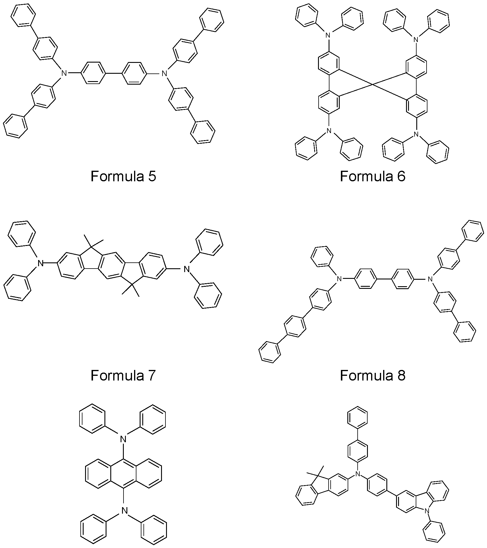
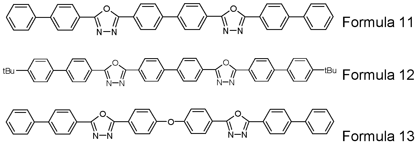

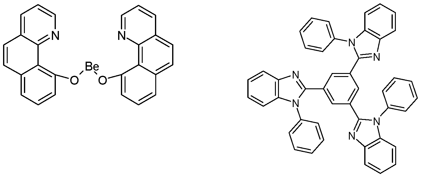


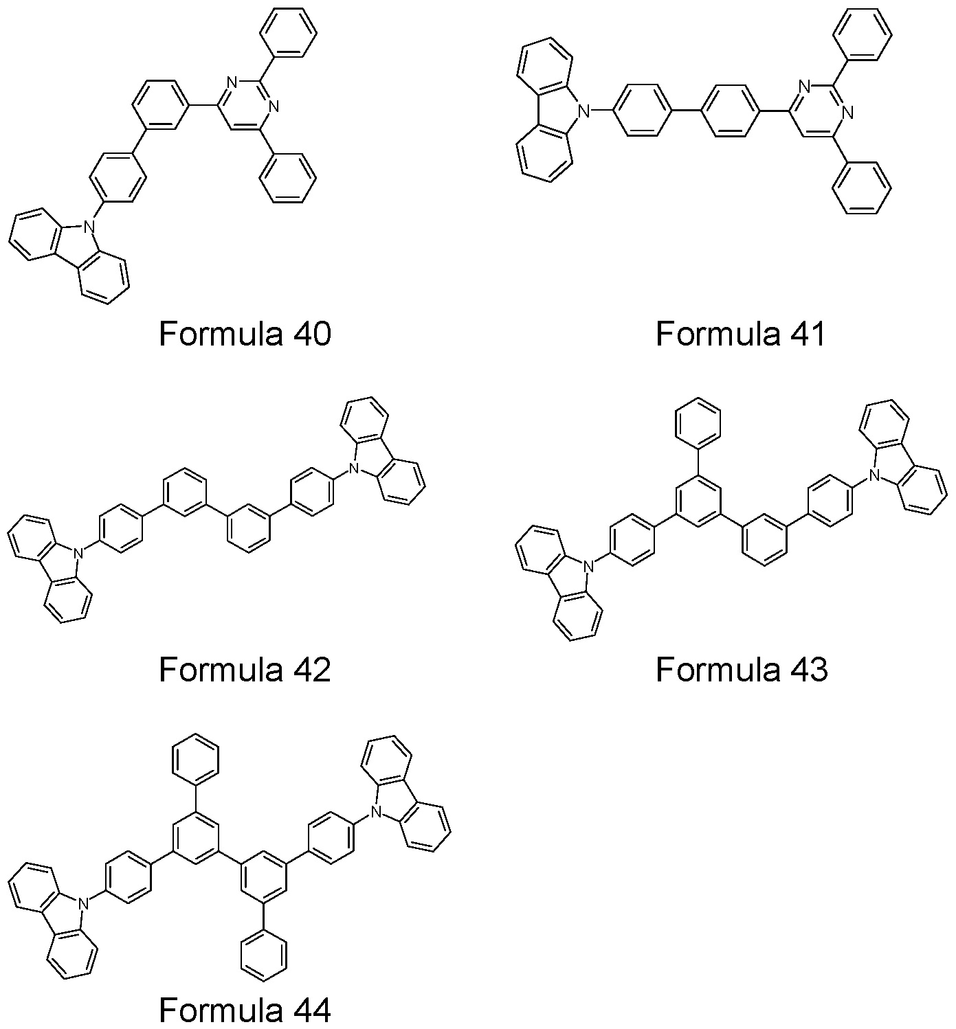


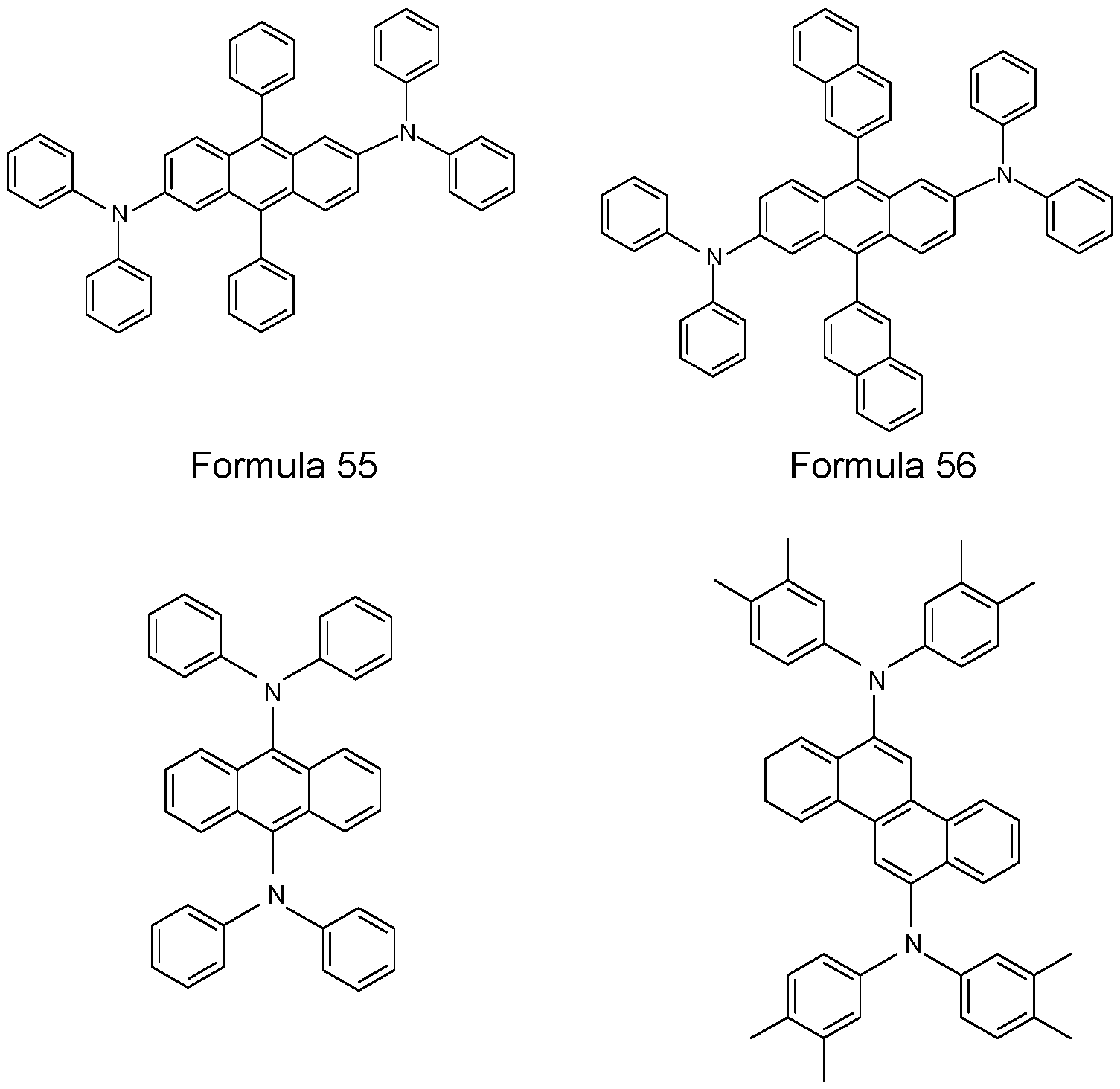
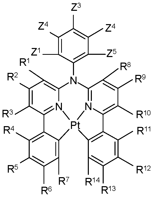

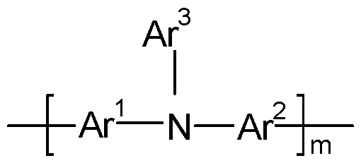

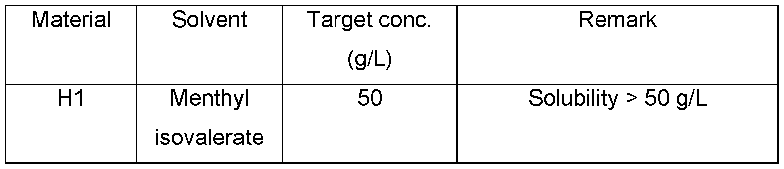


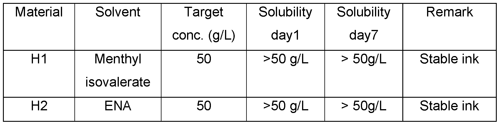
Claims
Priority Applications (3)
| Application Number | Priority Date | Filing Date | Title |
|---|---|---|---|
| CN202380045103.7A CN119256643A (en) | 2022-06-07 | 2023-06-05 | Method for printing functional layers of electronic devices by combining inks |
| JP2024572214A JP2025519518A (en) | 2022-06-07 | 2023-06-05 | Method for printing functional layers of electronic devices by combining inks - Patents.com |
| KR1020257000573A KR20250020648A (en) | 2022-06-07 | 2023-06-05 | Method for printing functional layers of electronic devices by combining inks |
Applications Claiming Priority (2)
| Application Number | Priority Date | Filing Date | Title |
|---|---|---|---|
| EP22177429.2 | 2022-06-07 | ||
| EP22177429 | 2022-06-07 |
Publications (1)
| Publication Number | Publication Date |
|---|---|
| WO2023237458A1 true WO2023237458A1 (en) | 2023-12-14 |
Family
ID=82258344
Family Applications (1)
| Application Number | Title | Priority Date | Filing Date |
|---|---|---|---|
| PCT/EP2023/064904 Ceased WO2023237458A1 (en) | 2022-06-07 | 2023-06-05 | Method of printing a functional layer of an electronic device by combining inks |
Country Status (5)
| Country | Link |
|---|---|
| JP (1) | JP2025519518A (en) |
| KR (1) | KR20250020648A (en) |
| CN (1) | CN119256643A (en) |
| TW (1) | TW202411366A (en) |
| WO (1) | WO2023237458A1 (en) |
Citations (188)
| Publication number | Priority date | Publication date | Assignee | Title |
|---|---|---|---|---|
| US3180730A (en) | 1959-04-09 | 1965-04-27 | Azoplate Corp | Material for electrophotographic purposes |
| US3526501A (en) | 1967-02-03 | 1970-09-01 | Eastman Kodak Co | 4-diarylamino-substituted chalcone containing photoconductive compositions for use in electrophotography |
| US3567450A (en) | 1968-02-20 | 1971-03-02 | Eastman Kodak Co | Photoconductive elements containing substituted triarylamine photoconductors |
| US3615404A (en) | 1968-04-25 | 1971-10-26 | Scott Paper Co | 1 3-phenylenediamine containing photoconductive materials |
| US3615402A (en) | 1969-10-01 | 1971-10-26 | Eastman Kodak Co | Tetra-substituted methanes as organic photoconductors |
| US3717462A (en) | 1969-07-28 | 1973-02-20 | Canon Kk | Heat treatment of an electrophotographic photosensitive member |
| US4127412A (en) | 1975-12-09 | 1978-11-28 | Eastman Kodak Company | Photoconductive compositions and elements |
| JPS54110837A (en) | 1978-02-17 | 1979-08-30 | Ricoh Co Ltd | Electrophotographic photoreceptor |
| JPS5646234A (en) | 1979-09-21 | 1981-04-27 | Ricoh Co Ltd | Electrophotographic receptor |
| US4356429A (en) | 1980-07-17 | 1982-10-26 | Eastman Kodak Company | Organic electroluminescent cell |
| US4539507A (en) | 1983-03-25 | 1985-09-03 | Eastman Kodak Company | Organic electroluminescent devices having improved power conversion efficiencies |
| JPS61210363A (en) | 1985-03-15 | 1986-09-18 | Canon Inc | electrophotographic photoreceptor |
| US4720432A (en) | 1987-02-11 | 1988-01-19 | Eastman Kodak Company | Electroluminescent device with organic luminescent medium |
| US4769292A (en) | 1987-03-02 | 1988-09-06 | Eastman Kodak Company | Electroluminescent device with modified thin film luminescent zone |
| JPS63295696A (en) | 1987-05-27 | 1988-12-02 | Mitsubishi Electric Corp | Phosphor for cathode ray tube |
| JPH0193191A (en) | 1987-10-02 | 1989-04-12 | Hikari Gijutsu Kenkyu Kaihatsu Kk | Manufacture of semiconductor laser |
| US4885221A (en) | 1986-12-06 | 1989-12-05 | Kabushiki Kaisha Toshiba | Electrophotography apparatus and electrophtographic process for developing positive image from positive or negative film |
| JPH024996A (en) | 1988-03-14 | 1990-01-09 | Nisshin Steel Co Ltd | Stainless steel having superior corrosion resistance |
| JPH0211399A (en) | 1988-06-30 | 1990-01-16 | Toshiharu Morikawa | Writing implement with function for illuminating pen point |
| JPH0210363A (en) | 1988-06-29 | 1990-01-16 | Nippon Telegr & Teleph Corp <Ntt> | Baking treatment of resist coated film |
| JPH0282263A (en) | 1988-09-20 | 1990-03-22 | Canon Inc | electrophotographic photoreceptor |
| JPH02204996A (en) | 1989-02-01 | 1990-08-14 | Nec Corp | Organic film type el element |
| US4950950A (en) | 1989-05-18 | 1990-08-21 | Eastman Kodak Company | Electroluminescent device with silazane-containing luminescent zone |
| JPH02282263A (en) | 1988-12-09 | 1990-11-19 | Nippon Oil Co Ltd | Hole transferring material |
| JPH038688A (en) | 1989-06-05 | 1991-01-16 | Mitsubishi Electric Corp | Elevator cab equipment |
| US5061569A (en) | 1990-07-26 | 1991-10-29 | Eastman Kodak Company | Electroluminescent device with organic electroluminescent medium |
| US5077142A (en) | 1989-04-20 | 1991-12-31 | Ricoh Company, Ltd. | Electroluminescent devices |
| US5121029A (en) | 1987-12-11 | 1992-06-09 | Idemitsu Kosan Co., Ltd. | Electroluminescence device having an organic electroluminescent element |
| US5130603A (en) | 1989-03-20 | 1992-07-14 | Idemitsu Kosan Co., Ltd. | Organic electroluminescence device |
| JPH04308688A (en) | 1991-04-08 | 1992-10-30 | Pioneer Electron Corp | Organic electroluminescence element |
| EP0569827A2 (en) | 1992-05-11 | 1993-11-18 | Idemitsu Kosan Company Limited | Organic electroluminescence device |
| EP0637899A1 (en) | 1993-08-02 | 1995-02-08 | BASF Aktiengesellschaft | Electroluminescent arrangement |
| EP0676461A2 (en) | 1994-04-07 | 1995-10-11 | Hoechst Aktiengesellschaft | Spiro compounds and their application as electroluminescence materials |
| JPH0853397A (en) | 1994-08-12 | 1996-02-27 | Toyo Ink Mfg Co Ltd | Diarylamine derivative, production method and use thereof |
| US5529853A (en) | 1993-03-17 | 1996-06-25 | Sanyo Electric Co., Ltd. | Organic electroluminescent element |
| JPH08292586A (en) | 1995-04-21 | 1996-11-05 | Hodogaya Chem Co Ltd | Electrophotographic photoreceptor |
| US5608287A (en) | 1995-02-23 | 1997-03-04 | Eastman Kodak Company | Conductive electron injector for light-emitting diodes |
| EP0278757B1 (en) | 1987-02-11 | 1997-11-12 | EASTMAN KODAK COMPANY (a New Jersey corporation) | Electroluminescent device with improved cathode |
| US5703436A (en) | 1994-12-13 | 1997-12-30 | The Trustees Of Princeton University | Transparent contacts for organic devices |
| US5707745A (en) | 1994-12-13 | 1998-01-13 | The Trustees Of Princeton University | Multicolor organic light emitting devices |
| EP0652273B1 (en) | 1993-11-09 | 1998-02-11 | Shinko Electric Industries Co. Ltd. | Organic material for electroluminescent device and electroluminescent device |
| DE19646119A1 (en) | 1996-11-08 | 1998-05-14 | Hoechst Ag | Electroluminescent device |
| US5766779A (en) | 1996-08-20 | 1998-06-16 | Eastman Kodak Company | Electron transporting materials for organic electroluminescent devices |
| EP0650955B1 (en) | 1993-11-01 | 1998-08-19 | Hodogaya Chemical Co., Ltd. | Amine compound and electro-luminescence device comprising same |
| US5844363A (en) | 1997-01-23 | 1998-12-01 | The Trustees Of Princeton Univ. | Vacuum deposited, non-polymeric flexible organic light emitting devices |
| JPH11837A (en) | 1997-06-11 | 1999-01-06 | Tokin Corp | Terminal assembly device for dielectric resonator |
| EP0891121A1 (en) | 1996-12-28 | 1999-01-13 | TDK Corporation | Organic electroluminescent elements |
| JP2913116B2 (en) | 1990-11-20 | 1999-06-28 | 株式会社リコー | EL device |
| JP2956965B2 (en) | 1996-09-26 | 1999-10-04 | ベクトン・ディキンソン・アンド・カンパニー | Needle assembly with locking enclosure |
| US5962631A (en) | 1995-07-28 | 1999-10-05 | The Dow Chemical Company | 2, 7-aryl-9-substituted fluorenes and 9-substituted fluorene oligomers and polymers |
| US6020078A (en) | 1998-12-18 | 2000-02-01 | Eastman Kodak Company | Green organic electroluminescent devices |
| EP1009041A2 (en) | 1998-12-09 | 2000-06-14 | Eastman Kodak Company | Electroluminescent device with improved hole transport layer |
| EP1029909A1 (en) | 1998-09-09 | 2000-08-23 | Idemitsu Kosan Co., Ltd. | Organic electroluminescence device and phenylenediamine derivative |
| US6127004A (en) | 1999-01-29 | 2000-10-03 | Eastman Kodak Company | Forming an amorphous fluorocarbon layer in electroluminescent devices |
| WO2000070655A2 (en) | 1999-05-13 | 2000-11-23 | The Trustees Of Princeton University | Very high efficiency organic light emitting devices based on electrophosphorescence |
| US6208077B1 (en) | 1998-11-05 | 2001-03-27 | Eastman Kodak Company | Organic electroluminescent device with a non-conductive fluorocarbon polymer layer |
| US6208075B1 (en) | 1998-11-05 | 2001-03-27 | Eastman Kodak Company | Conductive fluorocarbon polymer and method of making same |
| WO2001021729A1 (en) | 1999-09-21 | 2001-03-29 | Idemitsu Kosan Co., Ltd. | Organic electroluminescence and organic luminous medium |
| WO2001041512A1 (en) | 1999-12-01 | 2001-06-07 | The Trustees Of Princeton University | Complexes of form l2mx as phosphorescent dopants for organic leds |
| US6251531B1 (en) | 1995-02-25 | 2001-06-26 | Toyo Ink Manufacturing Co., Ltd. | Light-emitting material for organic electroluminescence device, and organic electroluminescence device for which the light-emitting material is adapted |
| JP2001267080A (en) | 2000-01-14 | 2001-09-28 | Toray Ind Inc | Light emission element |
| WO2001093642A1 (en) | 2000-05-30 | 2001-12-06 | The Trustees Of Princeton University | Phosphorescent organic light emitting devices |
| US20010053462A1 (en) | 2000-05-02 | 2001-12-20 | Masayuki Mishima | Light-emitting device |
| WO2002002714A2 (en) | 2000-06-30 | 2002-01-10 | E.I. Du Pont De Nemours And Company | Electroluminescent iridium compounds with fluorinated phenylpyridines, phenylpyrimidines, and phenylquinolines and devices made with such compounds |
| WO2002015645A1 (en) | 2000-08-11 | 2002-02-21 | The Trustees Of Princeton University | Organometallic compounds and emission-shifting organic electrophosphorescence |
| EP1191612A2 (en) | 2000-09-26 | 2002-03-27 | Canon Kabushiki Kaisha | Luminescence device, display apparatus and metal coordination compound |
| EP1191614A2 (en) | 2000-09-26 | 2002-03-27 | Canon Kabushiki Kaisha | Luminescence device and metal coordination compound therefor |
| EP1191613A2 (en) | 2000-09-26 | 2002-03-27 | Canon Kabushiki Kaisha | Luminescence device, display apparatus and metal coordination compound |
| EP1205527A1 (en) | 2000-03-27 | 2002-05-15 | Idemitsu Kosan Co., Ltd. | Organic electroluminescence device |
| WO2002043449A1 (en) | 2000-11-24 | 2002-05-30 | Toray Industries, Inc. | Luminescent element material and luminescent element comprising the same |
| WO2002077060A1 (en) | 2001-03-24 | 2002-10-03 | Covion Organic Semiconductors Gmbh | Conjugated polymers containing spirobifluorene units and fluorene units, and the use thereof |
| US20030027016A1 (en) | 2000-04-21 | 2003-02-06 | Tdk Corporation | Organic EL device |
| EP0906948B1 (en) | 1997-10-02 | 2003-02-12 | Xerox Corporation | Electroluminescent devices |
| WO2003020790A2 (en) | 2001-09-04 | 2003-03-13 | Covion Organic Semiconductors Gmbh | Conjugated polymers containing spirobifluorene units and the use thereof |
| US20030068528A1 (en) | 2001-08-29 | 2003-04-10 | Thompson Mark E. | Organic light emitting devices having carrier blocking layers comprising metal complexes |
| US6548956B2 (en) | 1994-12-13 | 2003-04-15 | The Trustees Of Princeton University | Transparent contacts for organic devices |
| JP2003115387A (en) | 2001-10-04 | 2003-04-18 | Junji Kido | Organic light emitting element and its manufacturing method |
| US6562485B2 (en) | 2001-01-26 | 2003-05-13 | Xerox Corporation | Electroluminescent (EL) devices |
| EP1162193B1 (en) | 1993-09-29 | 2003-05-14 | Idemitsu Kosan Company Limited | Acrylenediamine derivatives and organic electroluminescence device containing the same |
| EP0906947B1 (en) | 1997-10-02 | 2003-05-21 | Xerox Corporation | Indolocarbazole electroluminescent devices |
| US6576134B1 (en) | 1998-10-20 | 2003-06-10 | Erik Agner | Method for displacement chromatography |
| US6602540B2 (en) | 1996-08-12 | 2003-08-05 | The Trustees Of Princeton University | Fabrication of non-polymeric flexible organic light emitting devices |
| JP2003253145A (en) | 2002-02-28 | 2003-09-10 | Jsr Corp | Luminescent composition |
| EP1344788A1 (en) | 2002-03-15 | 2003-09-17 | Sumitomo Chemical Company, Limited | Conjugated polymer comprising dibenzothiophene- or dibenzofuran-units and their use in polymer LEDs |
| US20030175553A1 (en) | 2001-12-28 | 2003-09-18 | Thompson Mark E. | White light emitting oleds from combined monomer and aggregate emission |
| JP2003338375A (en) | 2002-03-14 | 2003-11-28 | Tdk Corp | Organic el element |
| WO2003099901A1 (en) | 2002-05-28 | 2003-12-04 | Sumitomo Chemical Company, Limited | Polymer and polymeric luminescent element comprising the same |
| US20030230989A1 (en) | 2002-06-17 | 2003-12-18 | Patent-Treuhand-Gesellschaft Fur Elektrisch Gluhlampen Mbh | Apparatus for operating discharge lamps |
| WO2004013073A1 (en) | 2002-08-02 | 2004-02-12 | Idemitsu Kosan Co., Ltd. | Anthracene derivatives and organic electroluminescent devices made by using the same |
| EP0908787B1 (en) | 1997-10-02 | 2004-04-14 | Xerox Corporation | Indolocarbazole Photoconductors |
| WO2004041901A1 (en) | 2002-11-08 | 2004-05-21 | Covion Organic Semiconductors Gmbh | Aryl-substituted polyindenofluorenes for use in organic electroluminiscent devices |
| WO2004058911A2 (en) | 2002-12-23 | 2004-07-15 | Covion Organic Semiconductors Gmbh | Organic electroluminescent element |
| JP2004200162A (en) | 2002-12-05 | 2004-07-15 | Toray Ind Inc | Light emitting element |
| DE10304819A1 (en) | 2003-02-06 | 2004-08-19 | Covion Organic Semiconductors Gmbh | Carbazole-containing conjugated polymers and blends, their preparation and use |
| US20040174116A1 (en) | 2001-08-20 | 2004-09-09 | Lu Min-Hao Michael | Transparent electrodes |
| WO2004081017A1 (en) | 2003-03-11 | 2004-09-23 | Covion Organic Semiconductors Gmbh | Metal complexes |
| JP2004288381A (en) | 2003-03-19 | 2004-10-14 | Konica Minolta Holdings Inc | Organic electroluminescent element |
| EP1469533A2 (en) | 2003-04-14 | 2004-10-20 | Kabushiki Kaisha Toyota Jidoshokki | Organic electroluminescent element that supresses generation of ultraviolet light and lighting system that has organic electroluminescent element |
| US20040209115A1 (en) | 2003-04-21 | 2004-10-21 | Thompson Mark E. | Organic light emitting devices with wide gap host materials |
| US20040209116A1 (en) | 2003-04-21 | 2004-10-21 | Xiaofan Ren | Organic light emitting devices with wide gap host materials |
| WO2004093207A2 (en) | 2003-04-15 | 2004-10-28 | Covion Organic Semiconductors Gmbh | Mixtures of matrix materials and organic semiconductors capable of emission, use of the same and electronic components containing said mixtures |
| JP2004311184A (en) | 2003-04-04 | 2004-11-04 | Junji Kido | Electron transportation material formed of multinucleate phenanthroline derivative, charge control material, and organic luminescent element using them |
| EP1478032A2 (en) | 2003-05-16 | 2004-11-17 | Kabushiki Kaisha Toyota Jidoshokki | Light emitting diode method for forming the same |
| EP1480280A2 (en) | 2003-05-23 | 2004-11-24 | Kabushiki Kaisha Toyota Jidoshokki | Organic electroluminescent device and method for manufacturing the same |
| US6824895B1 (en) | 2003-12-05 | 2004-11-30 | Eastman Kodak Company | Electroluminescent device containing organometallic compound with tridentate ligand |
| US6830828B2 (en) | 1998-09-14 | 2004-12-14 | The Trustees Of Princeton University | Organometallic complexes as phosphorescent emitters in organic LEDs |
| US6835469B2 (en) | 2001-10-17 | 2004-12-28 | The University Of Southern California | Phosphorescent compounds and devices comprising the same |
| WO2004113412A2 (en) | 2003-06-23 | 2004-12-29 | Covion Organic Semiconductors Gmbh | Polymer |
| WO2005003253A2 (en) | 2003-07-07 | 2005-01-13 | Covion Organic Semiconductors Gmbh | Mixtures of organic emissive semiconductors and matrix materials, their use and electronic components comprising said materials |
| WO2005014689A2 (en) | 2003-08-12 | 2005-02-17 | Covion Organic Semiconductors Gmbh | Conjugated polymers containing dihydrophenanthrene units and use thereof |
| DE10328627A1 (en) | 2003-06-26 | 2005-02-17 | Covion Organic Semiconductors Gmbh | New materials for electroluminescence |
| CN1583691A (en) | 2004-06-04 | 2005-02-23 | 友达光电股份有限公司 | Anthracene compound and organic electroluminescent device comprising the anthracene compound |
| US20050069729A1 (en) | 2003-09-30 | 2005-03-31 | Konica Minolta Holdings, Inc. | Organic electroluminescent element, illuminator, display and compound |
| US6878469B2 (en) | 2002-01-18 | 2005-04-12 | Lg Chem, Ltd. | Material for transporting electrons and organic electroluminescent display using the same |
| WO2005033244A1 (en) | 2003-09-29 | 2005-04-14 | Covion Organic Semiconductors Gmbh | Metal complexes |
| DE10343606A1 (en) | 2003-09-20 | 2005-04-14 | Covion Organic Semiconductors Gmbh | White-emitting copolymers, their preparation and use |
| WO2005033174A1 (en) | 2003-10-01 | 2005-04-14 | Sumitomo Chemical Company, Limited | Polymer light-emitting material and polymer light-emitting device |
| JP2005108556A (en) | 2003-09-29 | 2005-04-21 | Tdk Corp | Organic el element and organic el display |
| DE10349033A1 (en) | 2003-10-22 | 2005-05-25 | Covion Organic Semiconductors Gmbh | Organic semiconductor, for use in organic LEDs and solar cells and laser diodes, contains a polymer and structural units which emit light from the triplet state and a triplet emitter |
| WO2005056633A1 (en) | 2003-12-12 | 2005-06-23 | Sumitomo Chemical Company, Limited | Polymer compound and polymer light-emitting device using same |
| EP1551206A1 (en) | 2002-10-09 | 2005-07-06 | Idemitsu Kosan Co., Ltd. | Organic electroluminescent device |
| WO2005084082A1 (en) | 2004-02-20 | 2005-09-09 | Merck Patent Gmbh | Organic electronic devices |
| JP2005285661A (en) | 2004-03-30 | 2005-10-13 | Tdk Corp | Organic el element and organic el display |
| WO2005104264A1 (en) | 2004-04-26 | 2005-11-03 | Merck Patent Gmbh | Electroluminescent polymers and use therof |
| WO2005111172A2 (en) | 2004-05-11 | 2005-11-24 | Merck Patent Gmbh | Novel material mixtures for use in electroluminescence |
| JP2005347160A (en) | 2004-06-04 | 2005-12-15 | Konica Minolta Holdings Inc | Organic electroluminescence element, lighting device and display device |
| WO2006000389A1 (en) | 2004-06-26 | 2006-01-05 | Merck Patent Gmbh | Compounds for organic electronic devices |
| WO2006000388A1 (en) | 2004-06-26 | 2006-01-05 | Merck Patent Gmbh | Organic electroluminescent device |
| EP1617711A1 (en) | 2003-04-23 | 2006-01-18 | Konica Minolta Holdings, Inc. | Organic electroluminescent device and display |
| US20060043858A1 (en) | 2002-08-23 | 2006-03-02 | Idemitsu Kosan Co., Ltd. | Organic electroluminescence device and anthracene derivative |
| US20060061265A1 (en) | 2002-11-06 | 2006-03-23 | Hisayuki Kawamura | Aromatic amine derivative and organic electroluminescent element employing the same |
| US7029766B2 (en) | 2003-12-05 | 2006-04-18 | Eastman Kodak Company | Organic element for electroluminescent devices |
| WO2006048268A1 (en) | 2004-11-06 | 2006-05-11 | Merck Patent Gmbh | Organic electroluminescent device |
| WO2006052457A2 (en) | 2004-11-03 | 2006-05-18 | Sumation Co.Ltd. | New class of bridged biphenylene polymers |
| WO2006058737A1 (en) | 2004-12-01 | 2006-06-08 | Merck Patent Gmbh | Compounds for organic electronic devices |
| WO2006063852A1 (en) | 2004-12-18 | 2006-06-22 | Merck Patent Gmbh | Electroluminescent polymers and use thereof |
| US20060147747A1 (en) | 2003-03-13 | 2006-07-06 | Hiroshi Yamamoto | Nitrogen-containing heterocycle derivative and organic electroluminescent element using the same |
| US20060210830A1 (en) | 2005-03-15 | 2006-09-21 | Idemitsu Kosan Co., Ltd. | Aromatic amine derivative and organic electroluminescence device using the same |
| US20060222886A1 (en) | 2005-04-04 | 2006-10-05 | Raymond Kwong | Arylpyrene compounds |
| WO2006118345A1 (en) | 2005-04-28 | 2006-11-09 | Sumitomo Chemical Company, Limited | High-molecular compounds and high-molecular luminescent devices made by using the same |
| WO2006117052A1 (en) | 2005-05-03 | 2006-11-09 | Merck Patent Gmbh | Organic electroluminescent device and boric acid and borinic acid derivatives used therein |
| WO2006122630A1 (en) | 2005-05-20 | 2006-11-23 | Merck Patent Gmbh | Compounds for organic electronic devices |
| EP1731584A1 (en) | 2004-03-31 | 2006-12-13 | Konica Minolta Holdings, Inc. | Organic electroluminescent device material, organic electroluminescent device, display and illuminating device |
| US20070087219A1 (en) | 2005-10-19 | 2007-04-19 | Eastman Kodak Company | Electroluminescent device |
| WO2007043495A1 (en) | 2005-10-07 | 2007-04-19 | Sumitomo Chemical Company, Limited | Copolymer and polymer light emitting devices made by using the same |
| US20070092753A1 (en) | 2005-10-26 | 2007-04-26 | Eastman Kodak Company | Organic element for low voltage electroluminescent devices |
| US20070092755A1 (en) | 2005-10-26 | 2007-04-26 | Eastman Kodak Company | Organic element for low voltage electroluminescent devices |
| US20070122656A1 (en) | 2005-11-30 | 2007-05-31 | Eastman Kodak Company | Electroluminescent device containing an anthracene derivative |
| WO2007063754A1 (en) | 2005-12-01 | 2007-06-07 | Nippon Steel Chemical Co., Ltd. | Compound for organic electroluminescent element and organic electroluminescent element |
| DE102005058557A1 (en) | 2005-12-08 | 2007-06-14 | Merck Patent Gmbh | Organic electroluminescent device |
| US20070134514A1 (en) | 2005-12-14 | 2007-06-14 | Eastman Kodak Company | Electroluminescent host material |
| WO2007065549A1 (en) | 2005-12-08 | 2007-06-14 | Merck Patent Gmbh | Organic electroluminescent devices |
| US7250532B2 (en) | 2001-03-16 | 2007-07-31 | Idemitsu Kosan Co., Ltd. | Method for producing aromatic amino compound |
| US7250226B2 (en) | 2001-08-31 | 2007-07-31 | Nippon Hoso Kyokai | Phosphorescent compound, a phosphorescent composition and an organic light-emitting device |
| DE102006003710A1 (en) | 2006-01-26 | 2007-08-02 | Merck Patent Gmbh | New polymer containing an unit exhibiting electron injection and -conducting characteristics, useful for the preparation of a solution and formulation, and in an organic electronic devices, preferably organic optoelectronic device |
| JP2007197574A (en) | 2006-01-26 | 2007-08-09 | Showa Denko Kk | Polymer light-emitting material, organic electroluminescence element, and display device |
| JP2007211243A (en) | 2007-02-07 | 2007-08-23 | Showa Denko Kk | Polymer of polymerizable compound |
| WO2007095118A2 (en) | 2006-02-10 | 2007-08-23 | Universal Display Corporation | METAL COMPLEXES OF CYCLOMETALLATED IMIDAZO[1,2-f]PHENANTHRIDINE AND DIIMIDAZO[1,2-A:1',2'-C]QUINAZOLINE LIGANDS AND ISOELECTRONIC AND BENZANNULATED ANALOGS THEREOF |
| US20070205412A1 (en) | 2006-03-06 | 2007-09-06 | Jae-Soon Bae | Novel anthracene derivative and organic electronic device using the same |
| EP1834945A1 (en) | 2005-01-05 | 2007-09-19 | Idemitsu Kosan Co., Ltd. | Aromatic amine derivative and organic electroluminescent device using same |
| WO2007115610A1 (en) | 2006-04-01 | 2007-10-18 | Merck Patent Gmbh | Materials for organic electroluminescent devices |
| US20070252517A1 (en) | 2006-04-27 | 2007-11-01 | Eastman Kodak Company | Electroluminescent device including an anthracene derivative |
| WO2007131582A1 (en) | 2006-05-12 | 2007-11-22 | Merck Patent Gmbh | Indenofluorene polymer based organic semiconductor materials |
| EP1860097A1 (en) | 2005-03-18 | 2007-11-28 | Idemitsu Kosan Co., Ltd. | Aromatic amine derivative and organic electroluminescence device utilizing the same |
| US20070273272A1 (en) | 2006-04-03 | 2007-11-29 | Idemitsu Kosan Co., Ltd. | Benzanthracene derivative and electroluminescence device using the same |
| WO2007137725A1 (en) | 2006-05-31 | 2007-12-06 | Merck Patent Gmbh | New materials for organic electroluminescent devices |
| WO2007140847A1 (en) | 2006-06-02 | 2007-12-13 | Merck Patent Gmbh | Materials for organic electroluminescent devices |
| WO2008006449A1 (en) | 2006-07-11 | 2008-01-17 | Merck Patent Gmbh | Novel materials for organic electroluminescent devices |
| WO2008009343A1 (en) | 2006-07-21 | 2008-01-24 | Merck Patent Gmbh | Copolymers of indenofluorene and thiophene |
| US7326371B2 (en) | 2004-03-25 | 2008-02-05 | Eastman Kodak Company | Electroluminescent device with anthracene derivative host |
| US20080102311A1 (en) | 2006-08-04 | 2008-05-01 | Idemitsu Kosan Co., Ltd. | Material for organic electroluminescent element and organic electroluminescent element employing the same |
| WO2008056746A1 (en) | 2006-11-09 | 2008-05-15 | Nippon Steel Chemical Co., Ltd. | Compound for organic electroluminescent device and organic electroluminescent device |
| US20080113101A1 (en) | 2006-11-09 | 2008-05-15 | Idemitsu Kosan Co., Ltd. | Organic-electroluminescence-material-containing solution, method for forming thin film of organic electroluminescence material, thin film of organic electroluminescence material and organic electroluminescence device |
| US7378162B2 (en) | 2005-03-08 | 2008-05-27 | Lg Electronics Inc. | Organic electroluminescence devices using red phosphorescence compounds |
| DE102007002714A1 (en) | 2007-01-18 | 2008-07-31 | Merck Patent Gmbh | New materials for organic electroluminescent devices |
| US20080193796A1 (en) | 2006-11-20 | 2008-08-14 | Idemitsu Kosan Co., Ltd. | Organic electroluminescent device |
| EP1661888B1 (en) | 2004-11-29 | 2008-11-12 | Samsung SDI Co., Ltd. | Phenylcarbazole-based compound and organic electroluminescent device employing the same |
| WO2008146839A1 (en) | 2007-05-29 | 2008-12-04 | Nippon Steel Chemical Co., Ltd. | Compound for organic electroluminescent device and organic electroluminescent device |
| DE102007024850A1 (en) | 2007-05-29 | 2008-12-04 | Merck Patent Gmbh | New materials for organic electroluminescent devices |
| WO2008149691A1 (en) | 2007-05-30 | 2008-12-11 | Nippon Steel Chemical Co., Ltd. | Compound for organic electroluminescent device and organic electroluminescent device |
| EP1923448B1 (en) | 2006-11-09 | 2008-12-31 | Samsung SDI Co., Ltd. | Organic light emitting diode including organic layer comprising organic metal complex |
| US20090061681A1 (en) | 2007-09-05 | 2009-03-05 | Mcmunigal Tom | Electrical receptacle assembly |
| WO2009041635A1 (en) | 2007-09-28 | 2009-04-02 | Idemitsu Kosan Co., Ltd. | Organic el device |
| DE102008017591A1 (en) | 2008-04-07 | 2009-10-08 | Merck Patent Gmbh | New materials for organic electroluminescent devices |
| WO2011076314A1 (en) | 2009-12-22 | 2011-06-30 | Merck Patent Gmbh | Electroluminescent formulations |
| WO2016107668A1 (en) | 2014-12-30 | 2016-07-07 | Merck Patent Gmbh | Compositions comprising at least one polymer and at least one salt, and electroluminescent devices containing said compositions |
| JP2016195181A (en) * | 2015-03-31 | 2016-11-17 | セイコーエプソン株式会社 | LIGHT EMITTING DEVICE, LIGHT EMITTING DEVICE MANUFACTURING METHOD, AND ELECTRONIC DEVICE |
| CN108389979A (en) * | 2018-03-07 | 2018-08-10 | 京东方科技集团股份有限公司 | A kind of electroluminescence display panel, preparation method and display device |
-
2023
- 2023-06-02 TW TW112120637A patent/TW202411366A/en unknown
- 2023-06-05 KR KR1020257000573A patent/KR20250020648A/en active Pending
- 2023-06-05 CN CN202380045103.7A patent/CN119256643A/en active Pending
- 2023-06-05 JP JP2024572214A patent/JP2025519518A/en active Pending
- 2023-06-05 WO PCT/EP2023/064904 patent/WO2023237458A1/en not_active Ceased
Patent Citations (195)
| Publication number | Priority date | Publication date | Assignee | Title |
|---|---|---|---|---|
| US3180730A (en) | 1959-04-09 | 1965-04-27 | Azoplate Corp | Material for electrophotographic purposes |
| US3526501A (en) | 1967-02-03 | 1970-09-01 | Eastman Kodak Co | 4-diarylamino-substituted chalcone containing photoconductive compositions for use in electrophotography |
| US3567450A (en) | 1968-02-20 | 1971-03-02 | Eastman Kodak Co | Photoconductive elements containing substituted triarylamine photoconductors |
| US3615404A (en) | 1968-04-25 | 1971-10-26 | Scott Paper Co | 1 3-phenylenediamine containing photoconductive materials |
| US3717462A (en) | 1969-07-28 | 1973-02-20 | Canon Kk | Heat treatment of an electrophotographic photosensitive member |
| US3615402A (en) | 1969-10-01 | 1971-10-26 | Eastman Kodak Co | Tetra-substituted methanes as organic photoconductors |
| US4127412A (en) | 1975-12-09 | 1978-11-28 | Eastman Kodak Company | Photoconductive compositions and elements |
| JPS54110837A (en) | 1978-02-17 | 1979-08-30 | Ricoh Co Ltd | Electrophotographic photoreceptor |
| JPS5646234A (en) | 1979-09-21 | 1981-04-27 | Ricoh Co Ltd | Electrophotographic receptor |
| US4356429A (en) | 1980-07-17 | 1982-10-26 | Eastman Kodak Company | Organic electroluminescent cell |
| US4539507A (en) | 1983-03-25 | 1985-09-03 | Eastman Kodak Company | Organic electroluminescent devices having improved power conversion efficiencies |
| JPS61210363A (en) | 1985-03-15 | 1986-09-18 | Canon Inc | electrophotographic photoreceptor |
| US4885221A (en) | 1986-12-06 | 1989-12-05 | Kabushiki Kaisha Toshiba | Electrophotography apparatus and electrophtographic process for developing positive image from positive or negative film |
| US4720432A (en) | 1987-02-11 | 1988-01-19 | Eastman Kodak Company | Electroluminescent device with organic luminescent medium |
| EP0278757B1 (en) | 1987-02-11 | 1997-11-12 | EASTMAN KODAK COMPANY (a New Jersey corporation) | Electroluminescent device with improved cathode |
| US4769292A (en) | 1987-03-02 | 1988-09-06 | Eastman Kodak Company | Electroluminescent device with modified thin film luminescent zone |
| JPS63295696A (en) | 1987-05-27 | 1988-12-02 | Mitsubishi Electric Corp | Phosphor for cathode ray tube |
| JPH0193191A (en) | 1987-10-02 | 1989-04-12 | Hikari Gijutsu Kenkyu Kaihatsu Kk | Manufacture of semiconductor laser |
| US5121029A (en) | 1987-12-11 | 1992-06-09 | Idemitsu Kosan Co., Ltd. | Electroluminescence device having an organic electroluminescent element |
| JPH024996A (en) | 1988-03-14 | 1990-01-09 | Nisshin Steel Co Ltd | Stainless steel having superior corrosion resistance |
| JPH0210363A (en) | 1988-06-29 | 1990-01-16 | Nippon Telegr & Teleph Corp <Ntt> | Baking treatment of resist coated film |
| JPH0211399A (en) | 1988-06-30 | 1990-01-16 | Toshiharu Morikawa | Writing implement with function for illuminating pen point |
| JPH0282263A (en) | 1988-09-20 | 1990-03-22 | Canon Inc | electrophotographic photoreceptor |
| JPH02282263A (en) | 1988-12-09 | 1990-11-19 | Nippon Oil Co Ltd | Hole transferring material |
| JPH02204996A (en) | 1989-02-01 | 1990-08-14 | Nec Corp | Organic film type el element |
| US5130603A (en) | 1989-03-20 | 1992-07-14 | Idemitsu Kosan Co., Ltd. | Organic electroluminescence device |
| US5077142A (en) | 1989-04-20 | 1991-12-31 | Ricoh Company, Ltd. | Electroluminescent devices |
| US4950950A (en) | 1989-05-18 | 1990-08-21 | Eastman Kodak Company | Electroluminescent device with silazane-containing luminescent zone |
| JPH038688A (en) | 1989-06-05 | 1991-01-16 | Mitsubishi Electric Corp | Elevator cab equipment |
| US5061569A (en) | 1990-07-26 | 1991-10-29 | Eastman Kodak Company | Electroluminescent device with organic electroluminescent medium |
| JP2913116B2 (en) | 1990-11-20 | 1999-06-28 | 株式会社リコー | EL device |
| JPH04308688A (en) | 1991-04-08 | 1992-10-30 | Pioneer Electron Corp | Organic electroluminescence element |
| EP0569827A2 (en) | 1992-05-11 | 1993-11-18 | Idemitsu Kosan Company Limited | Organic electroluminescence device |
| US5529853A (en) | 1993-03-17 | 1996-06-25 | Sanyo Electric Co., Ltd. | Organic electroluminescent element |
| EP0637899A1 (en) | 1993-08-02 | 1995-02-08 | BASF Aktiengesellschaft | Electroluminescent arrangement |
| EP1162193B1 (en) | 1993-09-29 | 2003-05-14 | Idemitsu Kosan Company Limited | Acrylenediamine derivatives and organic electroluminescence device containing the same |
| EP0650955B1 (en) | 1993-11-01 | 1998-08-19 | Hodogaya Chemical Co., Ltd. | Amine compound and electro-luminescence device comprising same |
| EP0652273B1 (en) | 1993-11-09 | 1998-02-11 | Shinko Electric Industries Co. Ltd. | Organic material for electroluminescent device and electroluminescent device |
| EP0676461A2 (en) | 1994-04-07 | 1995-10-11 | Hoechst Aktiengesellschaft | Spiro compounds and their application as electroluminescence materials |
| JPH0853397A (en) | 1994-08-12 | 1996-02-27 | Toyo Ink Mfg Co Ltd | Diarylamine derivative, production method and use thereof |
| US5707745A (en) | 1994-12-13 | 1998-01-13 | The Trustees Of Princeton University | Multicolor organic light emitting devices |
| US5703436A (en) | 1994-12-13 | 1997-12-30 | The Trustees Of Princeton University | Transparent contacts for organic devices |
| US6548956B2 (en) | 1994-12-13 | 2003-04-15 | The Trustees Of Princeton University | Transparent contacts for organic devices |
| US5608287A (en) | 1995-02-23 | 1997-03-04 | Eastman Kodak Company | Conductive electron injector for light-emitting diodes |
| US6251531B1 (en) | 1995-02-25 | 2001-06-26 | Toyo Ink Manufacturing Co., Ltd. | Light-emitting material for organic electroluminescence device, and organic electroluminescence device for which the light-emitting material is adapted |
| JPH08292586A (en) | 1995-04-21 | 1996-11-05 | Hodogaya Chem Co Ltd | Electrophotographic photoreceptor |
| US5962631A (en) | 1995-07-28 | 1999-10-05 | The Dow Chemical Company | 2, 7-aryl-9-substituted fluorenes and 9-substituted fluorene oligomers and polymers |
| US6602540B2 (en) | 1996-08-12 | 2003-08-05 | The Trustees Of Princeton University | Fabrication of non-polymeric flexible organic light emitting devices |
| US5766779A (en) | 1996-08-20 | 1998-06-16 | Eastman Kodak Company | Electron transporting materials for organic electroluminescent devices |
| JP2956965B2 (en) | 1996-09-26 | 1999-10-04 | ベクトン・ディキンソン・アンド・カンパニー | Needle assembly with locking enclosure |
| DE19646119A1 (en) | 1996-11-08 | 1998-05-14 | Hoechst Ag | Electroluminescent device |
| EP0891121A1 (en) | 1996-12-28 | 1999-01-13 | TDK Corporation | Organic electroluminescent elements |
| US5844363A (en) | 1997-01-23 | 1998-12-01 | The Trustees Of Princeton Univ. | Vacuum deposited, non-polymeric flexible organic light emitting devices |
| JPH11837A (en) | 1997-06-11 | 1999-01-06 | Tokin Corp | Terminal assembly device for dielectric resonator |
| EP0906947B1 (en) | 1997-10-02 | 2003-05-21 | Xerox Corporation | Indolocarbazole electroluminescent devices |
| EP0906948B1 (en) | 1997-10-02 | 2003-02-12 | Xerox Corporation | Electroluminescent devices |
| EP0908787B1 (en) | 1997-10-02 | 2004-04-14 | Xerox Corporation | Indolocarbazole Photoconductors |
| EP1029909A1 (en) | 1998-09-09 | 2000-08-23 | Idemitsu Kosan Co., Ltd. | Organic electroluminescence device and phenylenediamine derivative |
| US7399537B2 (en) | 1998-09-09 | 2008-07-15 | Idemitsu Kosan Co., Ltd. | Organic electroluminescence device and phenylenediamine derivative |
| US6830828B2 (en) | 1998-09-14 | 2004-12-14 | The Trustees Of Princeton University | Organometallic complexes as phosphorescent emitters in organic LEDs |
| US6576134B1 (en) | 1998-10-20 | 2003-06-10 | Erik Agner | Method for displacement chromatography |
| US6208075B1 (en) | 1998-11-05 | 2001-03-27 | Eastman Kodak Company | Conductive fluorocarbon polymer and method of making same |
| US6208077B1 (en) | 1998-11-05 | 2001-03-27 | Eastman Kodak Company | Organic electroluminescent device with a non-conductive fluorocarbon polymer layer |
| EP1009041A2 (en) | 1998-12-09 | 2000-06-14 | Eastman Kodak Company | Electroluminescent device with improved hole transport layer |
| US6020078A (en) | 1998-12-18 | 2000-02-01 | Eastman Kodak Company | Green organic electroluminescent devices |
| US6127004A (en) | 1999-01-29 | 2000-10-03 | Eastman Kodak Company | Forming an amorphous fluorocarbon layer in electroluminescent devices |
| WO2000070655A2 (en) | 1999-05-13 | 2000-11-23 | The Trustees Of Princeton University | Very high efficiency organic light emitting devices based on electrophosphorescence |
| WO2001021729A1 (en) | 1999-09-21 | 2001-03-29 | Idemitsu Kosan Co., Ltd. | Organic electroluminescence and organic luminous medium |
| WO2001041512A1 (en) | 1999-12-01 | 2001-06-07 | The Trustees Of Princeton University | Complexes of form l2mx as phosphorescent dopants for organic leds |
| JP2001267080A (en) | 2000-01-14 | 2001-09-28 | Toray Ind Inc | Light emission element |
| EP1205527A1 (en) | 2000-03-27 | 2002-05-15 | Idemitsu Kosan Co., Ltd. | Organic electroluminescence device |
| US20030027016A1 (en) | 2000-04-21 | 2003-02-06 | Tdk Corporation | Organic EL device |
| US20010053462A1 (en) | 2000-05-02 | 2001-12-20 | Masayuki Mishima | Light-emitting device |
| WO2001093642A1 (en) | 2000-05-30 | 2001-12-06 | The Trustees Of Princeton University | Phosphorescent organic light emitting devices |
| WO2002002714A2 (en) | 2000-06-30 | 2002-01-10 | E.I. Du Pont De Nemours And Company | Electroluminescent iridium compounds with fluorinated phenylpyridines, phenylpyrimidines, and phenylquinolines and devices made with such compounds |
| WO2002015645A1 (en) | 2000-08-11 | 2002-02-21 | The Trustees Of Princeton University | Organometallic compounds and emission-shifting organic electrophosphorescence |
| EP1191614A2 (en) | 2000-09-26 | 2002-03-27 | Canon Kabushiki Kaisha | Luminescence device and metal coordination compound therefor |
| EP1191612A2 (en) | 2000-09-26 | 2002-03-27 | Canon Kabushiki Kaisha | Luminescence device, display apparatus and metal coordination compound |
| EP1191613A2 (en) | 2000-09-26 | 2002-03-27 | Canon Kabushiki Kaisha | Luminescence device, display apparatus and metal coordination compound |
| WO2002043449A1 (en) | 2000-11-24 | 2002-05-30 | Toray Industries, Inc. | Luminescent element material and luminescent element comprising the same |
| US6562485B2 (en) | 2001-01-26 | 2003-05-13 | Xerox Corporation | Electroluminescent (EL) devices |
| US7250532B2 (en) | 2001-03-16 | 2007-07-31 | Idemitsu Kosan Co., Ltd. | Method for producing aromatic amino compound |
| WO2002077060A1 (en) | 2001-03-24 | 2002-10-03 | Covion Organic Semiconductors Gmbh | Conjugated polymers containing spirobifluorene units and fluorene units, and the use thereof |
| US20040174116A1 (en) | 2001-08-20 | 2004-09-09 | Lu Min-Hao Michael | Transparent electrodes |
| US20030068528A1 (en) | 2001-08-29 | 2003-04-10 | Thompson Mark E. | Organic light emitting devices having carrier blocking layers comprising metal complexes |
| US7250226B2 (en) | 2001-08-31 | 2007-07-31 | Nippon Hoso Kyokai | Phosphorescent compound, a phosphorescent composition and an organic light-emitting device |
| WO2003020790A2 (en) | 2001-09-04 | 2003-03-13 | Covion Organic Semiconductors Gmbh | Conjugated polymers containing spirobifluorene units and the use thereof |
| JP2003115387A (en) | 2001-10-04 | 2003-04-18 | Junji Kido | Organic light emitting element and its manufacturing method |
| US6835469B2 (en) | 2001-10-17 | 2004-12-28 | The University Of Southern California | Phosphorescent compounds and devices comprising the same |
| US20030175553A1 (en) | 2001-12-28 | 2003-09-18 | Thompson Mark E. | White light emitting oleds from combined monomer and aggregate emission |
| US6878469B2 (en) | 2002-01-18 | 2005-04-12 | Lg Chem, Ltd. | Material for transporting electrons and organic electroluminescent display using the same |
| JP2003253145A (en) | 2002-02-28 | 2003-09-10 | Jsr Corp | Luminescent composition |
| JP2003338375A (en) | 2002-03-14 | 2003-11-28 | Tdk Corp | Organic el element |
| EP1344788A1 (en) | 2002-03-15 | 2003-09-17 | Sumitomo Chemical Company, Limited | Conjugated polymer comprising dibenzothiophene- or dibenzofuran-units and their use in polymer LEDs |
| WO2003099901A1 (en) | 2002-05-28 | 2003-12-04 | Sumitomo Chemical Company, Limited | Polymer and polymeric luminescent element comprising the same |
| US20030230989A1 (en) | 2002-06-17 | 2003-12-18 | Patent-Treuhand-Gesellschaft Fur Elektrisch Gluhlampen Mbh | Apparatus for operating discharge lamps |
| WO2004013073A1 (en) | 2002-08-02 | 2004-02-12 | Idemitsu Kosan Co., Ltd. | Anthracene derivatives and organic electroluminescent devices made by using the same |
| US20060043858A1 (en) | 2002-08-23 | 2006-03-02 | Idemitsu Kosan Co., Ltd. | Organic electroluminescence device and anthracene derivative |
| EP1551206A1 (en) | 2002-10-09 | 2005-07-06 | Idemitsu Kosan Co., Ltd. | Organic electroluminescent device |
| US20060061265A1 (en) | 2002-11-06 | 2006-03-23 | Hisayuki Kawamura | Aromatic amine derivative and organic electroluminescent element employing the same |
| WO2004041901A1 (en) | 2002-11-08 | 2004-05-21 | Covion Organic Semiconductors Gmbh | Aryl-substituted polyindenofluorenes for use in organic electroluminiscent devices |
| JP2004200162A (en) | 2002-12-05 | 2004-07-15 | Toray Ind Inc | Light emitting element |
| WO2004058911A2 (en) | 2002-12-23 | 2004-07-15 | Covion Organic Semiconductors Gmbh | Organic electroluminescent element |
| DE10304819A1 (en) | 2003-02-06 | 2004-08-19 | Covion Organic Semiconductors Gmbh | Carbazole-containing conjugated polymers and blends, their preparation and use |
| WO2004081017A1 (en) | 2003-03-11 | 2004-09-23 | Covion Organic Semiconductors Gmbh | Metal complexes |
| US20060147747A1 (en) | 2003-03-13 | 2006-07-06 | Hiroshi Yamamoto | Nitrogen-containing heterocycle derivative and organic electroluminescent element using the same |
| JP2004288381A (en) | 2003-03-19 | 2004-10-14 | Konica Minolta Holdings Inc | Organic electroluminescent element |
| JP2004311184A (en) | 2003-04-04 | 2004-11-04 | Junji Kido | Electron transportation material formed of multinucleate phenanthroline derivative, charge control material, and organic luminescent element using them |
| EP1469533A2 (en) | 2003-04-14 | 2004-10-20 | Kabushiki Kaisha Toyota Jidoshokki | Organic electroluminescent element that supresses generation of ultraviolet light and lighting system that has organic electroluminescent element |
| WO2004093207A2 (en) | 2003-04-15 | 2004-10-28 | Covion Organic Semiconductors Gmbh | Mixtures of matrix materials and organic semiconductors capable of emission, use of the same and electronic components containing said mixtures |
| US20040209115A1 (en) | 2003-04-21 | 2004-10-21 | Thompson Mark E. | Organic light emitting devices with wide gap host materials |
| US20040209116A1 (en) | 2003-04-21 | 2004-10-21 | Xiaofan Ren | Organic light emitting devices with wide gap host materials |
| EP1617710A1 (en) | 2003-04-23 | 2006-01-18 | Konica Minolta Holdings, Inc. | Material for organic electroluminescent device, organic electroluminescent device, illuminating device and display |
| EP1617711A1 (en) | 2003-04-23 | 2006-01-18 | Konica Minolta Holdings, Inc. | Organic electroluminescent device and display |
| EP1478032A2 (en) | 2003-05-16 | 2004-11-17 | Kabushiki Kaisha Toyota Jidoshokki | Light emitting diode method for forming the same |
| EP1480280A2 (en) | 2003-05-23 | 2004-11-24 | Kabushiki Kaisha Toyota Jidoshokki | Organic electroluminescent device and method for manufacturing the same |
| WO2004113412A2 (en) | 2003-06-23 | 2004-12-29 | Covion Organic Semiconductors Gmbh | Polymer |
| DE10328627A1 (en) | 2003-06-26 | 2005-02-17 | Covion Organic Semiconductors Gmbh | New materials for electroluminescence |
| WO2005003253A2 (en) | 2003-07-07 | 2005-01-13 | Covion Organic Semiconductors Gmbh | Mixtures of organic emissive semiconductors and matrix materials, their use and electronic components comprising said materials |
| DE10337346A1 (en) | 2003-08-12 | 2005-03-31 | Covion Organic Semiconductors Gmbh | Conjugated polymers containing dihydrophenanthrene units and their use |
| WO2005014689A2 (en) | 2003-08-12 | 2005-02-17 | Covion Organic Semiconductors Gmbh | Conjugated polymers containing dihydrophenanthrene units and use thereof |
| DE10343606A1 (en) | 2003-09-20 | 2005-04-14 | Covion Organic Semiconductors Gmbh | White-emitting copolymers, their preparation and use |
| JP2005108556A (en) | 2003-09-29 | 2005-04-21 | Tdk Corp | Organic el element and organic el display |
| WO2005033244A1 (en) | 2003-09-29 | 2005-04-14 | Covion Organic Semiconductors Gmbh | Metal complexes |
| WO2005039246A1 (en) | 2003-09-30 | 2005-04-28 | Konica Minolta Holdings, Inc. | Organic electroluminescent device, illuminating device, and display |
| US20050069729A1 (en) | 2003-09-30 | 2005-03-31 | Konica Minolta Holdings, Inc. | Organic electroluminescent element, illuminator, display and compound |
| WO2005033174A1 (en) | 2003-10-01 | 2005-04-14 | Sumitomo Chemical Company, Limited | Polymer light-emitting material and polymer light-emitting device |
| DE10349033A1 (en) | 2003-10-22 | 2005-05-25 | Covion Organic Semiconductors Gmbh | Organic semiconductor, for use in organic LEDs and solar cells and laser diodes, contains a polymer and structural units which emit light from the triplet state and a triplet emitter |
| US7029766B2 (en) | 2003-12-05 | 2006-04-18 | Eastman Kodak Company | Organic element for electroluminescent devices |
| US6824895B1 (en) | 2003-12-05 | 2004-11-30 | Eastman Kodak Company | Electroluminescent device containing organometallic compound with tridentate ligand |
| WO2005056633A1 (en) | 2003-12-12 | 2005-06-23 | Sumitomo Chemical Company, Limited | Polymer compound and polymer light-emitting device using same |
| WO2005084082A1 (en) | 2004-02-20 | 2005-09-09 | Merck Patent Gmbh | Organic electronic devices |
| WO2005084081A1 (en) | 2004-02-20 | 2005-09-09 | Merck Patent Gmbh | Organic electronic devices |
| US7326371B2 (en) | 2004-03-25 | 2008-02-05 | Eastman Kodak Company | Electroluminescent device with anthracene derivative host |
| JP2005285661A (en) | 2004-03-30 | 2005-10-13 | Tdk Corp | Organic el element and organic el display |
| EP1731584A1 (en) | 2004-03-31 | 2006-12-13 | Konica Minolta Holdings, Inc. | Organic electroluminescent device material, organic electroluminescent device, display and illuminating device |
| WO2005104264A1 (en) | 2004-04-26 | 2005-11-03 | Merck Patent Gmbh | Electroluminescent polymers and use therof |
| WO2005111172A2 (en) | 2004-05-11 | 2005-11-24 | Merck Patent Gmbh | Novel material mixtures for use in electroluminescence |
| CN1583691A (en) | 2004-06-04 | 2005-02-23 | 友达光电股份有限公司 | Anthracene compound and organic electroluminescent device comprising the anthracene compound |
| JP2005347160A (en) | 2004-06-04 | 2005-12-15 | Konica Minolta Holdings Inc | Organic electroluminescence element, lighting device and display device |
| WO2006000388A1 (en) | 2004-06-26 | 2006-01-05 | Merck Patent Gmbh | Organic electroluminescent device |
| WO2006000389A1 (en) | 2004-06-26 | 2006-01-05 | Merck Patent Gmbh | Compounds for organic electronic devices |
| WO2006052457A2 (en) | 2004-11-03 | 2006-05-18 | Sumation Co.Ltd. | New class of bridged biphenylene polymers |
| WO2006048268A1 (en) | 2004-11-06 | 2006-05-11 | Merck Patent Gmbh | Organic electroluminescent device |
| EP1661888B1 (en) | 2004-11-29 | 2008-11-12 | Samsung SDI Co., Ltd. | Phenylcarbazole-based compound and organic electroluminescent device employing the same |
| WO2006058737A1 (en) | 2004-12-01 | 2006-06-08 | Merck Patent Gmbh | Compounds for organic electronic devices |
| WO2006063852A1 (en) | 2004-12-18 | 2006-06-22 | Merck Patent Gmbh | Electroluminescent polymers and use thereof |
| EP1834945A1 (en) | 2005-01-05 | 2007-09-19 | Idemitsu Kosan Co., Ltd. | Aromatic amine derivative and organic electroluminescent device using same |
| US7378162B2 (en) | 2005-03-08 | 2008-05-27 | Lg Electronics Inc. | Organic electroluminescence devices using red phosphorescence compounds |
| US20060210830A1 (en) | 2005-03-15 | 2006-09-21 | Idemitsu Kosan Co., Ltd. | Aromatic amine derivative and organic electroluminescence device using the same |
| EP1860097A1 (en) | 2005-03-18 | 2007-11-28 | Idemitsu Kosan Co., Ltd. | Aromatic amine derivative and organic electroluminescence device utilizing the same |
| US20060222886A1 (en) | 2005-04-04 | 2006-10-05 | Raymond Kwong | Arylpyrene compounds |
| WO2006118345A1 (en) | 2005-04-28 | 2006-11-09 | Sumitomo Chemical Company, Limited | High-molecular compounds and high-molecular luminescent devices made by using the same |
| WO2006117052A1 (en) | 2005-05-03 | 2006-11-09 | Merck Patent Gmbh | Organic electroluminescent device and boric acid and borinic acid derivatives used therein |
| WO2006122630A1 (en) | 2005-05-20 | 2006-11-23 | Merck Patent Gmbh | Compounds for organic electronic devices |
| WO2007043495A1 (en) | 2005-10-07 | 2007-04-19 | Sumitomo Chemical Company, Limited | Copolymer and polymer light emitting devices made by using the same |
| US20070087219A1 (en) | 2005-10-19 | 2007-04-19 | Eastman Kodak Company | Electroluminescent device |
| US20070092755A1 (en) | 2005-10-26 | 2007-04-26 | Eastman Kodak Company | Organic element for low voltage electroluminescent devices |
| US20070092753A1 (en) | 2005-10-26 | 2007-04-26 | Eastman Kodak Company | Organic element for low voltage electroluminescent devices |
| US20070122656A1 (en) | 2005-11-30 | 2007-05-31 | Eastman Kodak Company | Electroluminescent device containing an anthracene derivative |
| WO2007063754A1 (en) | 2005-12-01 | 2007-06-07 | Nippon Steel Chemical Co., Ltd. | Compound for organic electroluminescent element and organic electroluminescent element |
| WO2007065678A1 (en) | 2005-12-08 | 2007-06-14 | Merck Patent Gmbh | Novel materials for organic electroluminiescent devices |
| EP1957606A1 (en) | 2005-12-08 | 2008-08-20 | Merck Patent GmbH | Novel materials for organic electroluminiescent devices |
| DE102005058557A1 (en) | 2005-12-08 | 2007-06-14 | Merck Patent Gmbh | Organic electroluminescent device |
| WO2007065549A1 (en) | 2005-12-08 | 2007-06-14 | Merck Patent Gmbh | Organic electroluminescent devices |
| US20070134514A1 (en) | 2005-12-14 | 2007-06-14 | Eastman Kodak Company | Electroluminescent host material |
| DE102006003710A1 (en) | 2006-01-26 | 2007-08-02 | Merck Patent Gmbh | New polymer containing an unit exhibiting electron injection and -conducting characteristics, useful for the preparation of a solution and formulation, and in an organic electronic devices, preferably organic optoelectronic device |
| JP2007197574A (en) | 2006-01-26 | 2007-08-09 | Showa Denko Kk | Polymer light-emitting material, organic electroluminescence element, and display device |
| WO2007095118A2 (en) | 2006-02-10 | 2007-08-23 | Universal Display Corporation | METAL COMPLEXES OF CYCLOMETALLATED IMIDAZO[1,2-f]PHENANTHRIDINE AND DIIMIDAZO[1,2-A:1',2'-C]QUINAZOLINE LIGANDS AND ISOELECTRONIC AND BENZANNULATED ANALOGS THEREOF |
| US20070205412A1 (en) | 2006-03-06 | 2007-09-06 | Jae-Soon Bae | Novel anthracene derivative and organic electronic device using the same |
| WO2007115610A1 (en) | 2006-04-01 | 2007-10-18 | Merck Patent Gmbh | Materials for organic electroluminescent devices |
| US20070273272A1 (en) | 2006-04-03 | 2007-11-29 | Idemitsu Kosan Co., Ltd. | Benzanthracene derivative and electroluminescence device using the same |
| US20070252517A1 (en) | 2006-04-27 | 2007-11-01 | Eastman Kodak Company | Electroluminescent device including an anthracene derivative |
| WO2007131582A1 (en) | 2006-05-12 | 2007-11-22 | Merck Patent Gmbh | Indenofluorene polymer based organic semiconductor materials |
| WO2007137725A1 (en) | 2006-05-31 | 2007-12-06 | Merck Patent Gmbh | New materials for organic electroluminescent devices |
| WO2007140847A1 (en) | 2006-06-02 | 2007-12-13 | Merck Patent Gmbh | Materials for organic electroluminescent devices |
| WO2008006449A1 (en) | 2006-07-11 | 2008-01-17 | Merck Patent Gmbh | Novel materials for organic electroluminescent devices |
| WO2008009343A1 (en) | 2006-07-21 | 2008-01-24 | Merck Patent Gmbh | Copolymers of indenofluorene and thiophene |
| US20080102311A1 (en) | 2006-08-04 | 2008-05-01 | Idemitsu Kosan Co., Ltd. | Material for organic electroluminescent element and organic electroluminescent element employing the same |
| WO2008056746A1 (en) | 2006-11-09 | 2008-05-15 | Nippon Steel Chemical Co., Ltd. | Compound for organic electroluminescent device and organic electroluminescent device |
| EP1923448B1 (en) | 2006-11-09 | 2008-12-31 | Samsung SDI Co., Ltd. | Organic light emitting diode including organic layer comprising organic metal complex |
| US20080113101A1 (en) | 2006-11-09 | 2008-05-15 | Idemitsu Kosan Co., Ltd. | Organic-electroluminescence-material-containing solution, method for forming thin film of organic electroluminescence material, thin film of organic electroluminescence material and organic electroluminescence device |
| US20080193796A1 (en) | 2006-11-20 | 2008-08-14 | Idemitsu Kosan Co., Ltd. | Organic electroluminescent device |
| DE102007002714A1 (en) | 2007-01-18 | 2008-07-31 | Merck Patent Gmbh | New materials for organic electroluminescent devices |
| JP2007211243A (en) | 2007-02-07 | 2007-08-23 | Showa Denko Kk | Polymer of polymerizable compound |
| WO2008146839A1 (en) | 2007-05-29 | 2008-12-04 | Nippon Steel Chemical Co., Ltd. | Compound for organic electroluminescent device and organic electroluminescent device |
| DE102007024850A1 (en) | 2007-05-29 | 2008-12-04 | Merck Patent Gmbh | New materials for organic electroluminescent devices |
| WO2008149691A1 (en) | 2007-05-30 | 2008-12-11 | Nippon Steel Chemical Co., Ltd. | Compound for organic electroluminescent device and organic electroluminescent device |
| US20090061681A1 (en) | 2007-09-05 | 2009-03-05 | Mcmunigal Tom | Electrical receptacle assembly |
| WO2009041635A1 (en) | 2007-09-28 | 2009-04-02 | Idemitsu Kosan Co., Ltd. | Organic el device |
| DE102008017591A1 (en) | 2008-04-07 | 2009-10-08 | Merck Patent Gmbh | New materials for organic electroluminescent devices |
| WO2011076314A1 (en) | 2009-12-22 | 2011-06-30 | Merck Patent Gmbh | Electroluminescent formulations |
| WO2016107668A1 (en) | 2014-12-30 | 2016-07-07 | Merck Patent Gmbh | Compositions comprising at least one polymer and at least one salt, and electroluminescent devices containing said compositions |
| JP2016195181A (en) * | 2015-03-31 | 2016-11-17 | セイコーエプソン株式会社 | LIGHT EMITTING DEVICE, LIGHT EMITTING DEVICE MANUFACTURING METHOD, AND ELECTRONIC DEVICE |
| CN108389979A (en) * | 2018-03-07 | 2018-08-10 | 京东方科技集团股份有限公司 | A kind of electroluminescence display panel, preparation method and display device |
Non-Patent Citations (14)
| Title |
|---|
| "Recent progress of molecular organic electroluminescent materials and devices", MAT. SCI. AND ENG. R, vol. 39, 2002, pages 143 - 222 |
| ADACHI ET AL., APPL. PHYS. LETT., vol. 78, 2001, pages 1622 - 1624 |
| B. O'REGANM. GRAETZEL, NATURE, vol. 353, 1991, pages 737 |
| BALDO ET AL., NATURE, vol. 395, 1998, pages 151 - 154 |
| BALDO, THOMPSON ET AL., NATURE, vol. 403, 2000, pages 750 - 753 |
| C.H. CHEN ET AL.: "Recent developments in organic electroluminescent materials", MACROMOL. SYMP., vol. 125, 1997, pages 1 - 48, XP000891579 |
| CINQUINO MARCO ET AL: "Effect of surface tension and drying time on inkjet-printed PEDOT:PSS for ITO-free OLED devices", JOURNAL OF SCIENCE: ADVANCED MATERIALS AND DEVICES, vol. 7, no. 1, 11 September 2021 (2021-09-11), pages 100394, XP093076382, ISSN: 2468-2179, Retrieved from the Internet <URL:https://www.sciencedirect.com/science/article/pii/S2468217921000708/pdfft?md5=b7568c1fd2a2222aaae678422e676bd1&pid=1-s2.0-S2468217921000708-main.pdf> DOI: 10.1016/j.jsamd.2021.09.001 * |
| F.C. KREBS, SOLAR ENERGY MATERIALS AND SOLAR CELLS, vol. 91, 2007, pages 953 |
| J. KIDO ET AL., APPL. PHYS. LETT., vol. 65, 1994, pages 2124 |
| JOHNSON ET AL., JACS, vol. 105, 1983, pages 1795 |
| KIDO ET AL., CHEM. LETT., vol. 657, 1990 |
| MA ET AL., SYNTH. METALS, vol. 94, 1998, pages 245 |
| SYNTH. METALS, vol. 91, no. 1-3, 1997, pages 209 |
| WRIGHTON, JACS, vol. 96, 1974, pages 998 |
Also Published As
| Publication number | Publication date |
|---|---|
| JP2025519518A (en) | 2025-06-26 |
| KR20250020648A (en) | 2025-02-11 |
| CN119256643A (en) | 2025-01-03 |
| TW202411366A (en) | 2024-03-16 |
Similar Documents
| Publication | Publication Date | Title |
|---|---|---|
| KR102436600B1 (en) | Formulation of organic functional materials | |
| US10808170B2 (en) | Esters containing non-aromatic cycles as solvents for OLED formulations | |
| KR102776731B1 (en) | Formulation of organic functional materials | |
| KR102346774B1 (en) | Formulation of organic functional materials | |
| KR102427363B1 (en) | Formulation of organic functional materials | |
| KR102451842B1 (en) | Formulation of organic functional materials | |
| EP3278377B1 (en) | Formulation of an organic functional material comprising a siloxane solvent | |
| US11046884B2 (en) | Formulation of an organic functional material comprising an epoxy group containing solvent | |
| KR102374183B1 (en) | Formulation of organic functional materials | |
| EP3807367B1 (en) | Formulation of an organic functional material | |
| EP3360175B1 (en) | Formulations comprising at least two organic semiconducting compounds and at least two solvents | |
| KR102486614B1 (en) | Formulation of organic functional materials | |
| WO2023237458A1 (en) | Method of printing a functional layer of an electronic device by combining inks | |
| WO2023012084A1 (en) | A printing method by combining inks | |
| KR20230114756A (en) | Ink Systems and Methods for Inkjet Printing |
Legal Events
| Date | Code | Title | Description |
|---|---|---|---|
| 121 | Ep: the epo has been informed by wipo that ep was designated in this application |
Ref document number: 23732404 Country of ref document: EP Kind code of ref document: A1 |
|
| WWE | Wipo information: entry into national phase |
Ref document number: 202380045103.7 Country of ref document: CN |
|
| WWE | Wipo information: entry into national phase |
Ref document number: 2024572214 Country of ref document: JP |
|
| WWP | Wipo information: published in national office |
Ref document number: 202380045103.7 Country of ref document: CN |
|
| ENP | Entry into the national phase |
Ref document number: 20257000573 Country of ref document: KR Kind code of ref document: A |
|
| WWE | Wipo information: entry into national phase |
Ref document number: 1020257000573 Country of ref document: KR |
|
| NENP | Non-entry into the national phase |
Ref country code: DE |
|
| WWP | Wipo information: published in national office |
Ref document number: 1020257000573 Country of ref document: KR |
|
| 122 | Ep: pct application non-entry in european phase |
Ref document number: 23732404 Country of ref document: EP Kind code of ref document: A1 |