WO2005003253A2 - Mixtures of organic emissive semiconductors and matrix materials, their use and electronic components comprising said materials - Google Patents
Mixtures of organic emissive semiconductors and matrix materials, their use and electronic components comprising said materials Download PDFInfo
- Publication number
- WO2005003253A2 WO2005003253A2 PCT/EP2004/007421 EP2004007421W WO2005003253A2 WO 2005003253 A2 WO2005003253 A2 WO 2005003253A2 EP 2004007421 W EP2004007421 W EP 2004007421W WO 2005003253 A2 WO2005003253 A2 WO 2005003253A2
- Authority
- WO
- WIPO (PCT)
- Prior art keywords
- formula
- occurrence
- different
- same
- atoms
- Prior art date
- Legal status (The legal status is an assumption and is not a legal conclusion. Google has not performed a legal analysis and makes no representation as to the accuracy of the status listed.)
- Ceased
Links
- 0 CC(c1c(C2(c3nnnnc3-3)c4c-3nnnn4)nc(C(c3nc(C4(c5nnnnc5-5)c6nnnnc6-c6nnnnc46)c-5nn3)I(*)=O)nn1)=C2N=N* Chemical compound CC(c1c(C2(c3nnnnc3-3)c4c-3nnnn4)nc(C(c3nc(C4(c5nnnnc5-5)c6nnnnc6-c6nnnnc46)c-5nn3)I(*)=O)nn1)=C2N=N* 0.000 description 1
- CVBVTDFTIPQJNI-UHFFFAOYSA-N O=S(c(cc1C23c4ccccc4-c4c2cccc4)ccc1-c1c3cccc1)c1ccc2-c3ccccc3C3(c4ccccc4-c4c3cccc4)c2c1 Chemical compound O=S(c(cc1C23c4ccccc4-c4c2cccc4)ccc1-c1c3cccc1)c1ccc2-c3ccccc3C3(c4ccccc4-c4c3cccc4)c2c1 CVBVTDFTIPQJNI-UHFFFAOYSA-N 0.000 description 1
Classifications
-
- H—ELECTRICITY
- H10—SEMICONDUCTOR DEVICES; ELECTRIC SOLID-STATE DEVICES NOT OTHERWISE PROVIDED FOR
- H10K—ORGANIC ELECTRIC SOLID-STATE DEVICES
- H10K85/00—Organic materials used in the body or electrodes of devices covered by this subclass
- H10K85/60—Organic compounds having low molecular weight
- H10K85/615—Polycyclic condensed aromatic hydrocarbons, e.g. anthracene
- H10K85/626—Polycyclic condensed aromatic hydrocarbons, e.g. anthracene containing more than one polycyclic condensed aromatic rings, e.g. bis-anthracene
-
- C—CHEMISTRY; METALLURGY
- C09—DYES; PAINTS; POLISHES; NATURAL RESINS; ADHESIVES; COMPOSITIONS NOT OTHERWISE PROVIDED FOR; APPLICATIONS OF MATERIALS NOT OTHERWISE PROVIDED FOR
- C09K—MATERIALS FOR MISCELLANEOUS APPLICATIONS, NOT PROVIDED FOR ELSEWHERE
- C09K11/00—Luminescent, e.g. electroluminescent, chemiluminescent materials
- C09K11/06—Luminescent, e.g. electroluminescent, chemiluminescent materials containing organic luminescent materials
-
- C—CHEMISTRY; METALLURGY
- C08—ORGANIC MACROMOLECULAR COMPOUNDS; THEIR PREPARATION OR CHEMICAL WORKING-UP; COMPOSITIONS BASED THEREON
- C08L—COMPOSITIONS OF MACROMOLECULAR COMPOUNDS
- C08L57/00—Compositions of unspecified polymers obtained by reactions only involving carbon-to-carbon unsaturated bonds
- C08L57/06—Homopolymers or copolymers containing elements other than carbon and hydrogen
- C08L57/12—Homopolymers or copolymers containing elements other than carbon and hydrogen containing nitrogen atoms
-
- C—CHEMISTRY; METALLURGY
- C09—DYES; PAINTS; POLISHES; NATURAL RESINS; ADHESIVES; COMPOSITIONS NOT OTHERWISE PROVIDED FOR; APPLICATIONS OF MATERIALS NOT OTHERWISE PROVIDED FOR
- C09B—ORGANIC DYES OR CLOSELY-RELATED COMPOUNDS FOR PRODUCING DYES, e.g. PIGMENTS; MORDANTS; LAKES
- C09B67/00—Influencing the physical, e.g. the dyeing or printing properties of dyestuffs without chemical reactions, e.g. by treating with solvents grinding or grinding assistants, coating of pigments or dyes; Process features in the making of dyestuff preparations; Dyestuff preparations of a special physical nature, e.g. tablets, films
- C09B67/0033—Blends of pigments; Mixtured crystals; Solid solutions
- C09B67/0034—Mixtures of two or more pigments or dyes of the same type
-
- H—ELECTRICITY
- H10—SEMICONDUCTOR DEVICES; ELECTRIC SOLID-STATE DEVICES NOT OTHERWISE PROVIDED FOR
- H10K—ORGANIC ELECTRIC SOLID-STATE DEVICES
- H10K10/00—Organic devices specially adapted for rectifying, amplifying, oscillating or switching; Organic capacitors or resistors having potential barriers
-
- C—CHEMISTRY; METALLURGY
- C09—DYES; PAINTS; POLISHES; NATURAL RESINS; ADHESIVES; COMPOSITIONS NOT OTHERWISE PROVIDED FOR; APPLICATIONS OF MATERIALS NOT OTHERWISE PROVIDED FOR
- C09K—MATERIALS FOR MISCELLANEOUS APPLICATIONS, NOT PROVIDED FOR ELSEWHERE
- C09K2211/00—Chemical nature of organic luminescent or tenebrescent compounds
- C09K2211/10—Non-macromolecular compounds
- C09K2211/1018—Heterocyclic compounds
- C09K2211/1022—Heterocyclic compounds bridged by heteroatoms, e.g. N, P, Si or B
-
- C—CHEMISTRY; METALLURGY
- C09—DYES; PAINTS; POLISHES; NATURAL RESINS; ADHESIVES; COMPOSITIONS NOT OTHERWISE PROVIDED FOR; APPLICATIONS OF MATERIALS NOT OTHERWISE PROVIDED FOR
- C09K—MATERIALS FOR MISCELLANEOUS APPLICATIONS, NOT PROVIDED FOR ELSEWHERE
- C09K2211/00—Chemical nature of organic luminescent or tenebrescent compounds
- C09K2211/18—Metal complexes
- C09K2211/185—Metal complexes of the platinum group, i.e. Os, Ir, Pt, Ru, Rh or Pd
-
- H—ELECTRICITY
- H10—SEMICONDUCTOR DEVICES; ELECTRIC SOLID-STATE DEVICES NOT OTHERWISE PROVIDED FOR
- H10K—ORGANIC ELECTRIC SOLID-STATE DEVICES
- H10K50/00—Organic light-emitting devices
- H10K50/10—OLEDs or polymer light-emitting diodes [PLED]
- H10K50/11—OLEDs or polymer light-emitting diodes [PLED] characterised by the electroluminescent [EL] layers
-
- H—ELECTRICITY
- H10—SEMICONDUCTOR DEVICES; ELECTRIC SOLID-STATE DEVICES NOT OTHERWISE PROVIDED FOR
- H10K—ORGANIC ELECTRIC SOLID-STATE DEVICES
- H10K85/00—Organic materials used in the body or electrodes of devices covered by this subclass
- H10K85/10—Organic polymers or oligomers
- H10K85/111—Organic polymers or oligomers comprising aromatic, heteroaromatic, or aryl chains, e.g. polyaniline, polyphenylene or polyphenylene vinylene
- H10K85/113—Heteroaromatic compounds comprising sulfur or selene, e.g. polythiophene
- H10K85/1135—Polyethylene dioxythiophene [PEDOT]; Derivatives thereof
-
- H—ELECTRICITY
- H10—SEMICONDUCTOR DEVICES; ELECTRIC SOLID-STATE DEVICES NOT OTHERWISE PROVIDED FOR
- H10K—ORGANIC ELECTRIC SOLID-STATE DEVICES
- H10K85/00—Organic materials used in the body or electrodes of devices covered by this subclass
- H10K85/30—Coordination compounds
- H10K85/321—Metal complexes comprising a group IIIA element, e.g. Tris (8-hydroxyquinoline) gallium [Gaq3]
- H10K85/324—Metal complexes comprising a group IIIA element, e.g. Tris (8-hydroxyquinoline) gallium [Gaq3] comprising aluminium, e.g. Alq3
-
- H—ELECTRICITY
- H10—SEMICONDUCTOR DEVICES; ELECTRIC SOLID-STATE DEVICES NOT OTHERWISE PROVIDED FOR
- H10K—ORGANIC ELECTRIC SOLID-STATE DEVICES
- H10K85/00—Organic materials used in the body or electrodes of devices covered by this subclass
- H10K85/30—Coordination compounds
- H10K85/341—Transition metal complexes, e.g. Ru(II)polypyridine complexes
- H10K85/342—Transition metal complexes, e.g. Ru(II)polypyridine complexes comprising iridium
-
- H—ELECTRICITY
- H10—SEMICONDUCTOR DEVICES; ELECTRIC SOLID-STATE DEVICES NOT OTHERWISE PROVIDED FOR
- H10K—ORGANIC ELECTRIC SOLID-STATE DEVICES
- H10K85/00—Organic materials used in the body or electrodes of devices covered by this subclass
- H10K85/60—Organic compounds having low molecular weight
- H10K85/631—Amine compounds having at least two aryl rest on at least one amine-nitrogen atom, e.g. triphenylamine
- H10K85/633—Amine compounds having at least two aryl rest on at least one amine-nitrogen atom, e.g. triphenylamine comprising polycyclic condensed aromatic hydrocarbons as substituents on the nitrogen atom
-
- Y—GENERAL TAGGING OF NEW TECHNOLOGICAL DEVELOPMENTS; GENERAL TAGGING OF CROSS-SECTIONAL TECHNOLOGIES SPANNING OVER SEVERAL SECTIONS OF THE IPC; TECHNICAL SUBJECTS COVERED BY FORMER USPC CROSS-REFERENCE ART COLLECTIONS [XRACs] AND DIGESTS
- Y02—TECHNOLOGIES OR APPLICATIONS FOR MITIGATION OR ADAPTATION AGAINST CLIMATE CHANGE
- Y02E—REDUCTION OF GREENHOUSE GAS [GHG] EMISSIONS, RELATED TO ENERGY GENERATION, TRANSMISSION OR DISTRIBUTION
- Y02E10/00—Energy generation through renewable energy sources
- Y02E10/50—Photovoltaic [PV] energy
- Y02E10/549—Organic PV cells
-
- Y—GENERAL TAGGING OF NEW TECHNOLOGICAL DEVELOPMENTS; GENERAL TAGGING OF CROSS-SECTIONAL TECHNOLOGIES SPANNING OVER SEVERAL SECTIONS OF THE IPC; TECHNICAL SUBJECTS COVERED BY FORMER USPC CROSS-REFERENCE ART COLLECTIONS [XRACs] AND DIGESTS
- Y02—TECHNOLOGIES OR APPLICATIONS FOR MITIGATION OR ADAPTATION AGAINST CLIMATE CHANGE
- Y02P—CLIMATE CHANGE MITIGATION TECHNOLOGIES IN THE PRODUCTION OR PROCESSING OF GOODS
- Y02P70/00—Climate change mitigation technologies in the production process for final industrial or consumer products
- Y02P70/50—Manufacturing or production processes characterised by the final manufactured product
Definitions
- the present invention describes the use of new materials and material mixtures in organic electronic components such as electroluminescent elements and their use in displays based thereon.
- OLEDs organic light-emitting diodes
- Full-color, large-area, high-resolution active matrix displays for a wide variety of applications (such as, for example, cell phones, PDAs, laptops, televisions and other applications).
- the operating voltage required is quite high, especially in the case of efficient phosphorescent OLEDs, and must therefore be reduced in order to improve the power efficiency. This is particularly important for portable applications.
- organometallic complexes which show phosphorescence instead of fluorescence [M. A. Baldo, S. Lamansky, P.E. Burrows, M.E. Thompson, S.R. Forrest, Applied Physics Letters, 1999, 75, 4-6].
- organometallic compounds For quantum mechanical reasons, up to four times quantum, energy and power efficiency is possible using organometallic compounds.
- the essential conditions for practical use are, in particular, a long operational lifespan, high stability against thermal stress and a low operating and operating voltage to enable mobile applications.
- organic electroluminescent devices The general structure of organic electroluminescent devices is described for example in US 4,539,507 and US 5,151, 629 and EP 01202358.
- An organic electroluminescent device usually consists of several layers which are applied to one another by means of vacuum methods or different printing methods. The individual layers are:
- a carrier plate ' substrate (usually glass or plastic films).
- a transparent anode usually indium tin oxide, ITO.
- a hole injection layer e.g. B. based on copper phthalocyanine (CuPc) or conductive polymers such as polyaniline (PANI) or polythiophene derivatives (such as PEDOT).
- CuPc copper phthalocyanine
- PANI polyaniline
- PEDOT polythiophene derivatives
- One or more hole transport layers usually based on triarylamine derivatives, eg. B. 4,4 ', 4 "tris (N-1-naphthyl-N-phenylamino) triphenylamine (NaphDATA) as the first layer and N, N'-di (naphth-1-yl) - N, N '-diphenyl-benzidine (NPB) as a second hole transport layer.
- triarylamine derivatives eg. B. 4,4 ', 4 "tris (N-1-naphthyl-N-phenylamino) triphenylamine (NaphDATA) as the first layer and N, N'-di (naphth-1-yl) - N, N '-diphenyl-benzidine (NPB) as a second hole transport layer.
- emission Layer EML
- this layer can partially coincide with layers 4 to 8, but usually consists of fluorescent dyes, e.g. B. N, N'-diphenyl-quinachdon (QA), or phosphorescent dyes, e.g. B. tris (phenylpyridyl) iridium (lr (PPy) 3 ) or tris (2-benzothiophenylpyridyl) iridium (lr (BTP) 3 ), doped matrix materials such as 4,4'-bis (carbazol-9-yl ) -biphenyl (CBP).
- the emission layer can also consist of polymers, mixtures of polymers, mixtures of polymers and low-molecular compounds or mixtures of different low-molecular compounds.
- An electron transport layer mostly based on aluminum tris-8-hydroxyquinolinate (AIQ 3 ).
- EIL electron injection layer
- a thin layer consisting of a material with a high dielectric constant, such as.
- a cathode here metals, metal combinations or metal alloys with a low work function are generally used.
- the anode consists, for. B made of AI / Ni / NiOx or Al / Pt / PtOx or other metal / metal oxide combinations that have a HOMO greater than 5 eV.
- the cathode consists of the same materials that are described in items 9 and 10, with the difference that the metal, such as. B. Ca, Ba, Mg, Al, In, etc., is very thin and therefore transparent.
- the layer thickness is less than 50 nm, better less than 30 nm, even better less than 10 nm.
- Another can be applied to this transparent cathode transparent material are applied, e.g. B. ITO (indium tin oxide), IZO (indium zinc oxide), etc.
- the matrix material of the emission layer plays a special role.
- the matrix material has to transport holes and / or charge
- Matrix materials, the carbazole units, such as. B. contain the commonly used CBP, but have some disadvantages in practice. These can be seen, among other things, in the often short to very short lifespan of the devices manufactured with them and the often high operating voltages that lead to low power efficiencies. Furthermore, it has been shown that for energetic reasons, CBP is unsuitable for blue-emitting electroluminescent devices, which results in poor efficiency. In addition, the structure of the devices is very complex if CBP is used as the matrix material, since a hole blocking layer and an electron transport layer must also be used. If these additional layers are not used, e.g. B. by Adachi et al.
- the mixtures according to the invention are preferably those which contain at least one matrix material A whose glass transition temperature T g (measured as the pure substance) is greater than 70 ° C.
- the matrix material A is preferably at least one compound of the formulas (1) to (4),
- L is the same or different at every occurrence P, As, Sb or Bi;
- M is the same or different at each occurrence S, Se, Te;
- X is the same or different at each occurrence O, S, Se or NR 3 ;
- R 10 are the same or different at each occurrence H or an aliphatic or aromatic hydrocarbon radical with 1 to 20 C atoms.
- An aromatic or heteroaromatic system in the sense of this invention is to be understood as a system which does not necessarily only contain aromatic or heteroaromatic groups, but also in which several aromatic or heteroaromatic groups by a short non-aromatic unit ( ⁇ 10% of the Atoms, preferably ⁇ 5% of the atoms), such as sp 3 -hybridized C, O, N, etc., can be interrupted.
- a short non-aromatic unit ⁇ 10% of the Atoms, preferably ⁇ 5% of the atoms
- systems such as 9,9'-spirobifluorene, 9,9-diarylfluorene, triarylamine, diphenyl ether, etc. should also be understood as aromatic systems.
- Organic electroluminescent devices which contain at least one compound of the formulas (5) to (37) as matrix material A are likewise preferred,
- a matrix material A which contains at least one compound of the formula (38) or (39), Formula (38) Formula (39) where o is a number from 5 to 5000000 and where the symbols m, R 1 and R 3 have the meanings given under formula (1) to (4).
- a matrix material A which contains at least one 9,9'-spirobifluorene unit.
- a matrix material A which contains at least one compound of the formulas (40) to (48),
- Ar is the same or different in each occurrence, a mono- or divalent aromatic or heteroaromatic ring system with 2 to 40 C atoms, preferably with 4 to 30 C atoms, one or more H atoms being replaced by F, Cl, Br, I. and which can be substituted by one or more non-aromatic radicals R 1 , it being possible for a plurality of substituents R 1 , both on the same ring and on different rings, to form a further mono- or polycyclic, aliphatic or aromatic ring system; p is the same or different at each occurrence 0 or 1.
- Mixtures which contain one or more of the matrix materials A described above by formulas (1) to (48) are particularly preferred, characterized in that
- M is S at every occurrence
- X is O every time it occurs
- Z is the same or different on each occurrence of CR 1 or N;
- Mixtures which contain one or more of the matrix materials A described above by formulas (1) to (48) are particularly preferred, characterized in that they are chiral.
- the matrix materials A according to the invention described above, e.g. B. according to Examples 50 to 53, can, for example, as co-monomers to produce appropriate conjugated, partially conjugated or non-conjugated polymers or as the core of dendrimers, for. B. according to Examples 54 and 55, use.
- the corresponding further functionalization (polymerization or conversion to dendrimers) is preferably carried out via the halogen functionality.
- the above-mentioned compounds can be converted into soluble polyfluorenes (e.g. according to EP 842208 or WO 00/22026), poly-spirobifluorenes (e.g. according to EP 707020 or EP 894107), poly-para-phenylenes (e.g.
- poly-carbazoles poly-vinylcarbazoles (PVK) or polythiophenes (e.g. according to EP 1028136).
- VK poly-vinylcarbazoles
- EP 1028136 polythiophenes
- the matrix materials A according to the invention can also be obtained, for example, from Reaction types can be further functionalized and thus converted into expanded Mat xmate alien A.
- the functionalization with arylboronic acids according to SUZUKI or with amines according to HARTWIG-BUCHWALD can be mentioned here as an example.
- the matrix materials A according to the invention or their mixtures or the polymers or dendrimers containing the matrix materials A or their mixtures or mixtures of the polymers or dendrimers containing the matrix materials A and the matrix materials A, optionally together with the emitters B generally known methods known to those skilled in the art, such as vacuum evaporation, evaporation in a carrier gas stream or also from solution by spin coating or with various printing processes (for example ink-jet printing, offset printing, LITI printing, etc.) in the form of a film Applied substrate.
- the matrix materials described above are used in combination with phosphorescence emitters.
- the organic electroluminescent devices represented in this way are distinguished by the fact that they contain at least one compound as emitter B, which is characterized in that, with suitable excitation, it emits light, preferably in the visible range, and also at least one atom of atomic number greater than 20, preferably greater 38 and less than 84, particularly preferably greater than 56 and less than 80.
- Particularly preferred mixtures contain at least one compound of the formula (49) to (52) as emitter B, Formula (49) Formula (50)
- DCy is the same or different with each occurrence a cyclic group which contains at least one donor atom, preferably nitrogen or phosphorus, via which the cyclic group is bonded to the metal and which in turn can carry one or more substituents R 11 ; the groups DCy and CCy are connected to one another via a covalent bond;
- CCy is the same or different with each occurrence a cyclic group which contains a carbon atom via which the cyclic group is bonded to the metal and which in turn can carry one or more substituents R 11 ;
- R 4 , R 5 , R 6 are the same or different with each occurrence H or an aliphatic or aromatic hydrocarbon radical with 1 to 20 C atoms.
- Examples of the emitters described above can be found, for example, in applications WO 00/70655, WO 01/41512, WO 02/02714, WO 02/15645, EP 1191613, EP 1191612 and EP 1191614; these are hereby considered as part of the registration via quotation.
- the mixture according to the invention contains between 1 and 99% by weight, preferably between 3 and 95% by weight, particularly preferably between 5 and 50% by weight, in particular between 7 and 20% by weight of emitter B based on the total mixture of emitter B and matrix material A.
- the present invention further relates to electronic components, in particular organic electroluminescent devices (OLED), organic solar cells (O-SCs), organic field-effect transistors (O-FETs), organic optical detectors, organic photoreceptors in electrophotography or organic laser diodes (O-lasers). containing the mixture of matrix material A and emission material B according to the invention
- Organic electroluminescent devices which have at least one emitting layer (EML) containing a mixture of at least one are particularly preferred
- Matrix material A and at least one emission material B capable of emission are Matrix material A and at least one emission material B capable of emission
- B is a compound, characterized in that it emits light with suitable excitation and which contains at least one element of an atomic number greater than 20.
- EML emitting layer
- the organic electroluminescent device can contain further layers, such as, for. B. hole injection layer, hole transport layer, hole blocking layer, electron transport layer and / or electron injection layer.
- hole injection layer hole transport layer
- hole blocking layer hole blocking layer
- electron transport layer electron transport layer
- / or electron injection layer it should be pointed out that each of these layers does not necessarily have to be present. It has been shown, for example, that an OLED which neither contains a separate hole blocking layer nor a separate electron transport layer continues to show very good results in electroluminescence, in particular a significantly higher power efficiency. This is particularly surprising since a corresponding OLED with a carbazole-containing matrix material without a hole blocking and electron transport layer shows only very low performance efficiencies, in particular at high brightness (cf. Adachi et al., Organic Electronics 2001, 2, 37).
- Another object of the invention is therefore an organic electroluminescent device containing a mixture according to the invention which directly adjoins the electron transport layer without using a hole blocking layer or which directly adjoins the electron injection layer or the cathode without using a hole blocking layer and an electron transport layer.
- the organic electroluminescent devices show higher efficiency, significantly longer life and, in particular without using a hole blocking and electron transport layer, significantly lower operating voltages and higher power efficiencies than OLEDs according to the prior art, which use CBP as the matrix material.
- CBP CBP
- the preferred embodiments of the mixtures of matrix material A and emission material B according to the invention are also for the electronic components according to the invention, in particular for the organic electroluminescent devices (OLED), organic solar cells (O-SCs), organic field effect transistors (O-FETs), organic optical detectors, organic Photoreceptors for electrophotography or organic laser diodes (O-lasers). To avoid unnecessary repetitions, we do not list them again here.
- OLED organic electroluminescent devices
- O-SCs organic solar cells
- O-FETs organic field effect transistors
- O-FETs organic optical detectors
- O-lasers organic Photoreceptors for electrophotography or organic laser diodes
- the matrix materials A according to the invention lead to a significant improvement in the efficiency and the lifespan of the electroluminescent devices produced with them.
- the matrix materials A can be used to produce blue-emitting electroluminescent devices.
- the sublimated samples were first at a heating rate of 10 K / min. heated from 25 ° C to the melting point of the substance +50 K. They were then cooled to 25 ° C. from this temperature at a heating rate of 80 K / min.
- the glass transition temperature T g was measured by reheating at a heating rate of 10 K / min to a temperature of 50 K above the melting point of the substance using a device from Netzsch DCS 204 (TASC 414/4 Controler and CC200 C Controler).
- Example 1 Bis (9,9'-spirobifluoren-2-yl) phenylphosphine oxide (matrix material M1)
- the colorless residue was taken up in 1000 ml of dichloromethane, the suspension was washed three times with 300 ml of water. The organic phase was separated off, dried over sodium sulfate and then concentrated. The colorless residue was dissolved in 1000 ml of ethyl acetate and added dropwise with good stirring using a
- Example 2 Bis (9,9 'spirobifluorene-2-yl) sulfoxide (matrix material M2)
- Example 3 1,1'-binaphthyl-2,2'-bis (diphenylphosphine oxide) (matrix material M3)
- Matrix material M1 Matrix material M2
- OLEDs were produced using the general process outlined below. In individual cases, of course, this had to be adapted to the respective circumstances (e.g. layer thickness variation in order to achieve optimum efficiency or color). Electroluminescent devices according to the invention can be represented, for example, as described in the unpublished application DE 10317556.3. 3. Device examples
- the first example describes a comparison standard according to the prior art, in which the emitter layer consists of the host material CBP and the guest material lr (PPy) 3 . Furthermore, an OLED with an emitter layer consisting of the host material bis (9,9'-spirobifluoren-2-yl) phenylphosphine oxide (synthesis see example 1) and the guest material lr (PPy) 3 (synthesized according to WO 02/060910) is described , as well as OLEDs with other host materials according to the invention. OLEDs with the following structure were produced:
- PEDOT 60 nm spun on water; PEDOT obtained from H.C. Starck; poly [3,4-ethylenedioxy-2,5-thiophene])
- NaphDATA 20 nm (evaporated; NaphDATA purchased from SynTec; 4,4 ', 4 "-Tris (N-1-naphthyl-N-phenylamino) -triphenylamine
- Emitter layer CPB 20 nm (evaporated; CPB obtained from ALDRICH and further purified, finally sublimed twice; 4,4'-bis (N-carbazolyl) biphenyl) comparison standard)
- BCP 10 nm (evaporated; BCP obtained from ABCR, used as received; 2,9-dimethyl-4,7-diphenyl-1, 10-phenanthroline); not used in all examples; A1Q 3 10 nm (evaporated: AIQ 3 purchased from SynTec; Ths (quinolinolato) aluminum (III)); Ba-Al does not use 3 nm Ba in all of the examples, 150 nm Al as cathode thereon.
- OLEDs which have not yet been optimized, have been characterized as standard; For this, the electroluminescence spectra, the efficiency (measured in cd / A) depending on the brightness, calculated from current-voltage-brightness characteristics (IUL characteristics), and the service life were determined.
- the OLEDs both the reference standard (OLED with CBP), as well as the OLEDs with bis (9,9 'spirobifluorene-2-yl) phenylphosphine, with bis (9,9' spirobifluorene-2-yl) sulfoxide and treated with 1 , 1 '-Binaphthyl-2,2'-bis (diphenylphosphine oxide) as host material show green emission, resulting from the dopant lr (PPy) 3 .
- OLEDs produced with the host material CBP (Table 1, Example 1), an efficiency of approximately 20 to 25 cd / A is typically obtained under the conditions described above, and 4.8 V are required for the reference luminance of 100 cd / m 2 .
- OLEDs produced with the host material bis (9,9 -spirobifluoren- '. 2-yl) phenylphosphine a maximum efficiency of about 40 cd / A, where the required voltage for the reference luminance of 100 cd / m 2 even 4.0 V is reduced (Fig. 1 and Table 1, Example 2a).
- HBL hole blocking layer
- ETL electron transport layer
- the figure shows the course of the brightness, measured in cd / m 2 , over time.
- the lifespan is the time after which 50% of the initial luminance is reached.
- a lifespan of approx. 30 h is obtained with an initial brightness of 3500 cd / m 2 , which corresponds to an accelerated measurement, since the initial brightness is significantly higher than the brightness which is typical for active matrix controlled display applications required.
- OLEDs with bis (9,9 'spirobifluorene-2-yI) sulfoxide (Example 3a and 3b) and 1, 1'-binaphthyl-2,2'-bis (diphenylphosphine) (example 4a and 4b) as the host material exhibit both with HBL and ETL as well as without HBL and ETL also an improved lifespan in comparison to OLEDs with CBP (example 1) as host material. All examples are summarized in Table 1.
- M1 bis (9,9 '-spiro-bifluorene-2-yl) phenylphosphine oxide
- M2 bis (9,9' spirobifluorene-2-yl) sulfoxide
- M3 1, 1'-binaphthyl-2,2 ' -bis (diphenylphosphine)
Landscapes
- Chemical & Material Sciences (AREA)
- Organic Chemistry (AREA)
- Engineering & Computer Science (AREA)
- Materials Engineering (AREA)
- Chemical Kinetics & Catalysis (AREA)
- Physics & Mathematics (AREA)
- Spectroscopy & Molecular Physics (AREA)
- Health & Medical Sciences (AREA)
- Polymers & Plastics (AREA)
- Medicinal Chemistry (AREA)
- Electroluminescent Light Sources (AREA)
- Organic Low-Molecular-Weight Compounds And Preparation Thereof (AREA)
- Thin Film Transistor (AREA)
- Photovoltaic Devices (AREA)
- Photoreceptors In Electrophotography (AREA)
- Luminescent Compositions (AREA)
Abstract
Description
Mischungen von organischen zur Emission befähigten Halbleitern und Matrixmaterialien, deren Verwendung und Elektronikbauteile enthaltend dieseMixtures of organic semiconductors and matrix materials capable of emission, their use and electronic components containing them
Die vorliegende Erfindung beschreibt die Verwendung neuer Materialien und Materialmischungen in organischen elektronischen Bauteilen wie Elektrolumineszenzelementen und deren Verwendung in darauf basierenden Displays.The present invention describes the use of new materials and material mixtures in organic electronic components such as electroluminescent elements and their use in displays based thereon.
In einer Reihe von verschiedenartigen Anwendungen, die im weitesten Sinne der Elektronikindustrie zugerechnet werden können, ist der Einsatz organischer Halbleiter als Wirkkomponenten (= Funktionsmaterialien) seit geraumer Zeit Realität bzw. wird in naher Zukunft erwartet.In a number of different applications, which can be broadly attributed to the electronics industry, the use of organic semiconductors as active components (= functional materials) has been a reality for some time or is expected in the near future.
So finden schon seit etlichen Jahren lichtsensitive organische Materialien (z. B. Phthalocyanine) sowie organische Ladungstransportmaterialien (i. d. R. Lochtransporter auf Triarylaminbasis) Verwendung in Kopiergeräten.For several years now, light-sensitive organic materials (e.g. phthalocyanines) and organic charge transport materials (usually triarylamine-based hole transporters) have been used in copiers.
Der Einsatz spezieller halbleitender organischer Verbindungen, die zum Teil auch zur Emission von Licht im sichtbaren Spektralbereich befähigt sind, steht gerade am Anfang der Markteinführung, zum Beispiel in organischen Elektrolumineszenzvorrichtungen. Deren Einzelbauteile, die Organischen-Lichtemittierenden-Dioden (OLEDs), besitzen ein sehr breites Anwendungsspektrum als:The use of special semiconducting organic compounds, some of which are also capable of emitting light in the visible spectral range, is just at the beginning of the market launch, for example in organic electroluminescent devices. Their individual components, the organic light-emitting diodes (OLEDs), have a very wide range of applications as:
1. weiße oder farbige Hinterleuchtungen für monochrome oder mehrfarbige Anzeigeelemente (wie z. B. im Taschenrechner, für Mobiltelefone und andere tragbare Anwendungen),1. white or colored backlighting for monochrome or multicolored display elements (such as in a calculator, for mobile telephones and other portable applications),
2. großflächige Anzeigen (wie z. B. Verkehrsschilder, Plakate und ändere Anwendungen),2. large-scale advertisements (such as traffic signs, posters and other applications),
3. Beleuchtungselemente in allen Farben und Formen,3. lighting elements in all colors and shapes,
4. monochrome oder vollfarbige Passiv-Matrix-Displays für tragbare Anwendungen (wie z. B. Mobiltelefone, PDAs, Camcorder und andere Anwendungen),4. monochrome or full-color passive matrix displays for portable applications (such as, for example, mobile telephones, PDAs, camcorders and other applications),
5. vollfarbige großflächige hochauflösende Aktiv-Matrix-Displays für verschiedenste Anwendungen (wie z. B. Mobiltelefone, PDAs, Laptops, Fernseher und andere Anwendungen).5. Full-color, large-area, high-resolution active matrix displays for a wide variety of applications (such as, for example, cell phones, PDAs, laptops, televisions and other applications).
Bei diesen Anwendungen ist die Entwicklung teilweise bereits sehr weit fortgeschritten; dennoch besteht immer noch großer Bedarf an technischen Verbesserungen.The development of these applications is in some cases very advanced; however, there is still a great need for technical improvements.
Für einfachere OLEDs enthaltende Vorrichtungen ist die Markteinführung bereits erfolgt, wie die Auto-Radios der Firma Pioneer oder eine Digitalkamera der Firma Kodak mit "Organischem Display" belegen. Allerdings gibt es immer noch erhebliche Probleme, die einer dringenden Verbesserung bedürfen:The market launch for devices containing simple OLEDs has already taken place, as evidenced by the car radios from Pioneer or a digital camera from Kodak with an "organic display". However, there are still significant problems that need urgent improvement:
1. So ist v. a. die operative Lebensdauer von OLEDs immer noch gering, so daß bis dato nur einfache Anwendungen kommerziell realisiert werden können.1. So v. a. the operational life of OLEDs is still short, so that only simple applications can be realized commercially up to now.
BESTATIGUNGSKOPIE 2. Die Effizienzen von OLEDs sind zwar akzeptabel, aber auch hier sind natürlich - gerade für tragbare Anwendungen ("portable applications") - immer noch Verbesserungen erwünscht.BESTATIGUNGSKOPIE 2. The efficiencies of OLEDs are acceptable, but improvements are of course still desired, especially for portable applications.
3. Die Alterungsprozesse gehen i. d. R. mit einem Anstieg der Spannung einher. Dieser Effekt macht spannungsgetriebene organische Elektrolumineszenzvorrichtungen, z. B. Displays oder Anzeige-Elemente, schwierig bzw. unmöglich. Eine stromgetriebene Ansteuerung ist aber gerade in diesem Fall aufwendiger und teurer.3. The aging processes go i. d. Usually accompanied by an increase in voltage. This effect makes voltage driven organic electroluminescent devices, e.g. B. displays or display elements, difficult or impossible. In this case, however, a current-driven control is more complex and expensive.
4. Die benötigte Betriebsspannung ist gerade bei effizienten phosphoreszierenden OLEDs recht hoch und muß daher verringert werden, um die Leistungseffizienz zu verbessern. Das ist gerade für tragbare Anwendungen von großer Bedeutung.4. The operating voltage required is quite high, especially in the case of efficient phosphorescent OLEDs, and must therefore be reduced in order to improve the power efficiency. This is particularly important for portable applications.
5. Der benötigte Betriebsstrom ist ebenfalls in den letzten Jahren verringert worden, muß aber noch weiter verringert werden, um die Leistungseffizienz zu verbessern. Das ist gerade für tragbare Anwendungen besonders wichtig.5. The operating current required has also been reduced in recent years, but must be further reduced to improve performance efficiency. This is especially important for portable applications.
6. Durch die Vielfalt an Schichten ist der Aufbau der OLEDs komplex und technologisch sehr aufwendig. Daher wäre es wünschenswert, OLEDs mit einem einfacheren Schichtaufbau, der weniger Schichten benötigt, mit weiterhin guten Eigenschaften realisieren zu können.6. Due to the variety of layers, the structure of the OLEDs is complex and technologically very complex. It would therefore be desirable to be able to implement OLEDs with a simpler layer structure, which requires fewer layers, and still have good properties.
Die oben unter 1. bis 7. genannten Gründe machen Verbesserungen bei der Herstellung von OLEDs notwendig.The reasons given under 1 to 7 above make improvements in the production of OLEDs necessary.
Eine Entwicklung hierzu, die sich in den letzten Jahren abzeichnet, ist der Einsatz von metallorganischen Komplexen, die Phosphoreszenz statt Fluoreszenz zeigen [M. A. Baldo, S. Lamansky, P. E. Burrows, M. E. Thompson, S. R. Forrest, Applied Physics Letters, 1999, 75, 4-6]. Aus quantenmechanischen Gründen ist unter Verwendung metallorganischer Verbindungen eine bis zu vierfache Quanten-, Energie- und Leistungseffizienz möglich. Ob sich diese neue Entwicklung durchsetzen wird, hängt zum einen stark davon ab, ob entsprechende Device-Kompositionen gefunden werden können, die diese Vorteile (Triplett- Emission = Phosphoreszenz gegenüber Singulett-Emission = Fluoreszenz) auch in den OLEDs umsetzen können. Als wesentliche Bedingungen für die praktische Anwendung sind hier insbesondere eine hohe operative Lebensdauer, eine hohe Stabilität gegenüber Temperaturbelastung und eine niedrige Einsatz- und Betriebsspannung, um mobile Applikationen zu ermöglichen, zu nennen.One development that has emerged in recent years is the use of organometallic complexes which show phosphorescence instead of fluorescence [M. A. Baldo, S. Lamansky, P.E. Burrows, M.E. Thompson, S.R. Forrest, Applied Physics Letters, 1999, 75, 4-6]. For quantum mechanical reasons, up to four times quantum, energy and power efficiency is possible using organometallic compounds. On the one hand, whether this new development will prevail depends heavily on whether suitable device compositions can be found that can also implement these advantages (triplet emission = phosphorescence over singlet emission = fluorescence) in the OLEDs. The essential conditions for practical use are, in particular, a long operational lifespan, high stability against thermal stress and a low operating and operating voltage to enable mobile applications.
Der allgemeine Aufbau von organischen Elektrolumineszenzvorrichtunge ist beispielsweise in US 4,539,507 und US 5,151 ,629 sowie EP 01202358 beschrieben. Üblicherweise besteht eine organische Elektrolumineszenzvorrichtung aus mehreren Schichten, die mittels Vakuummethoden oder unterschiedlicher Druckmethoden aufeinander aufgebracht werden. Diese Schichten sind im einzelnen:The general structure of organic electroluminescent devices is described for example in US 4,539,507 and US 5,151, 629 and EP 01202358. An organic electroluminescent device usually consists of several layers which are applied to one another by means of vacuum methods or different printing methods. The individual layers are:
1. Eine Trägerplatte =' Substrat (üblicherweise Glas oder Kunststoffolien).1. A carrier plate = ' substrate (usually glass or plastic films).
2. Eine transparente Anode (üblicherweise Indium-Zinn-Oxid, ITO). 3. Eine Lochinjektions-Schicht (Hole Injection Layer = HIL): z. B. auf der Basis von Kupfer- phthalocyanin (CuPc) oder leitfähigen Polymeren, wie Polyanilin (PANI) oder Polythiophen-Derivaten (wie PEDOT).2. A transparent anode (usually indium tin oxide, ITO). 3. A hole injection layer (HIL): e.g. B. based on copper phthalocyanine (CuPc) or conductive polymers such as polyaniline (PANI) or polythiophene derivatives (such as PEDOT).
4. Eine oder mehrere Lochtransport-Schichten (Hole Transport Layer = HTL): üblicherweise auf der Basis von Triarylamin-Derivaten, z. B. 4,4',4"-Tris(N-1-naphthyl-N- phenyl-amino)-triphenylamin (NaphDATA) als erste Schicht und N,N'-Di(naphth-1-yl)- N,N'-diphenyl-benzidin (NPB) als zweite Lochtransportschicht.4. One or more hole transport layers (HTL): usually based on triarylamine derivatives, eg. B. 4,4 ', 4 "tris (N-1-naphthyl-N-phenylamino) triphenylamine (NaphDATA) as the first layer and N, N'-di (naphth-1-yl) - N, N '-diphenyl-benzidine (NPB) as a second hole transport layer.
5. Eine oder mehrere Emissions-Schichten (Emission Layer = EML): diese Schicht (bzw. Schichten) kann teilweise mit den Schichten 4 bis 8 zusammenfallen, besteht aber üblicherweise aus mit Fluoreszenzfarbstoffen, z. B. N,N'-Diphenyl-chinachdon (QA), oder Phosphoreszenzfarbstoffen, z. B. Tris(phenylpyridyl)-iridium (lr(PPy)3) oder Tris(2- benzothiophenyl-pyridyl)-iridium (lr(BTP)3), dotierten Matrixmaterialien, wie 4,4'-Bis(carbazol-9-yl)-biphenyl (CBP). Die Emissionsschicht kann aber auch aus Polymeren, Mischungen von Polymeren, Mischungen von Polymeren und niedermolekularen Verbindungen oder Mischungen verschiedener niedermolekularer Verbindungen bestehen.5. One or more emission layers (Emission Layer = EML): this layer (or layers) can partially coincide with layers 4 to 8, but usually consists of fluorescent dyes, e.g. B. N, N'-diphenyl-quinachdon (QA), or phosphorescent dyes, e.g. B. tris (phenylpyridyl) iridium (lr (PPy) 3 ) or tris (2-benzothiophenylpyridyl) iridium (lr (BTP) 3 ), doped matrix materials such as 4,4'-bis (carbazol-9-yl ) -biphenyl (CBP). However, the emission layer can also consist of polymers, mixtures of polymers, mixtures of polymers and low-molecular compounds or mixtures of different low-molecular compounds.
6. Eine Lochblockier-Schicht (Hole-Blocking-Layer = HBL): diese Schicht kann teilweise mit den Schichten 7 und 8 zusammenfallen. Sie besteht üblicherweise aus BCP (2,9-Dimethyl-4,7-diphenyl-1 ,10-phenanthrolin = Bathocuproin) oder Bis-(2-methyl-8- chinolinolato)-4-(phenylphenolato)-aluminium(lll) (BAIq).6. A hole blocking layer (HBL): this layer can partially coincide with layers 7 and 8. It usually consists of BCP (2,9-dimethyl-4,7-diphenyl-1, 10-phenanthroline = bathocuproin) or bis (2-methyl-8-quinolinolato) -4- (phenylphenolato) aluminum (III) ( BAlq).
7. Eine Elektronentransport-Schicht (Electron Transport Layer = ETL): meist auf Basis von Aluminium-tris-8-hydroxychinolinat (AIQ3).7. An electron transport layer (ETL): mostly based on aluminum tris-8-hydroxyquinolinate (AIQ 3 ).
8. Eine Elektroneninjektions-Schicht (Electron injection JLayer = EIL): diese Schicht kann teilweise mit Schicht 4, 5, 6 und 7 zusammenfallen, bzw. es wird ein kleiner Teil der Kathode speziell behandelt bzw. speziell abgeschieden.8. An electron injection layer (Electron injection JLayer = EIL): this layer can partially coincide with layers 4, 5, 6 and 7, or a small part of the cathode is specially treated or specially deposited.
9. Eine weitere Elektroneninjektions-Schicht (Electron Injection Layer = EIL): ein dünne Schicht bestehend aus einem Material mit einer hohen Dielektrizitätskonstanten, wie z. B. LiF, Li2O, BaF2, MgO, NaF.9. Another electron injection layer (EIL): a thin layer consisting of a material with a high dielectric constant, such as. B. LiF, Li 2 O, BaF 2 , MgO, NaF.
10. Eine Kathode: hier werden in der Regel Metalle, Metallkombinationen oder Metallegierungen mit niedriger Austrittsarbeit verwendet, so z. B. Ca, Ba, Cs, Mg, AI, In, Mg/Ag.10. A cathode: here metals, metal combinations or metal alloys with a low work function are generally used. B. Ca, Ba, Cs, Mg, Al, In, Mg / Ag.
Diese ganze Vorrichtung wird entsprechend (je nach Anwendung) strukturiert, kontaktiert und schließlich auch hermetisch versiegelt, da sich i. d. R. die Lebensdauer derartiger Vorrichtungen bei Anwesenheit von Wasser und/oder Luft drastisch verkürzt. Das Gleiche gilt auch für sogenannte invertierte Strukturen, bei denen das Licht aus der Kathode ausgekoppelt wird. Bei diesen invertierten OLEDs besteht die Anode z. B aus AI/Ni/NiOx oder Al/Pt/PtOx oder anderen Metall/Metalloxid-Kombinationen, die ein HOMO größer 5 eV besitzen. Die Kathode besteht dabei aus den gleichen Materialien, die in Punkt 9 und 10 beschrieben sind, mit dem Unterschied, daß das Metall, wie z. B. Ca, Ba, Mg, AI, In usw., sehr dünn und damit transparent ist. Die Schichtdicke liegt unter 50 nm, besser unter 30 nm, noch besser unter 10 nm. Auf diese transparente Kathode kann noch ein weiteres transparentes Material aufgebracht werden, z. B. ITO (Indium-Zinn-Oxid), IZO (Indium-Zink- Oxid) usw..This entire device is structured (depending on the application), contacted and finally also hermetically sealed, since the life of such devices is usually drastically shortened in the presence of water and / or air. The same also applies to so-called inverted structures, in which the light is coupled out of the cathode. In these inverted OLEDs, the anode consists, for. B made of AI / Ni / NiOx or Al / Pt / PtOx or other metal / metal oxide combinations that have a HOMO greater than 5 eV. The cathode consists of the same materials that are described in items 9 and 10, with the difference that the metal, such as. B. Ca, Ba, Mg, Al, In, etc., is very thin and therefore transparent. The layer thickness is less than 50 nm, better less than 30 nm, even better less than 10 nm. Another can be applied to this transparent cathode transparent material are applied, e.g. B. ITO (indium tin oxide), IZO (indium zinc oxide), etc.
Organische Elektrolumineszenzvorrichtungen, bei denen die Emissionsschicht (EML) aus mehr als einer Substanz besteht, sind schon seit längerem bekannt.Organic electroluminescent devices in which the emission layer (EML) consists of more than one substance have long been known.
Im oben genannten Aufbau kommt dem Matrixmaterial der Emissions-Schicht (EML) eine besondere Rolle zu. Das Matrixmaterial muß den Ladungstransport von Löchern und/oderIn the structure mentioned above, the matrix material of the emission layer (EML) plays a special role. The matrix material has to transport holes and / or charge
Elektronen ermöglichen oder verbessern und/oder die Ladungsträgerrekombination ermöglichen oder verbessern und gegebenenfalls die bei der Rekombination entstehendeEnable or improve electrons and / or enable or improve charge recombination and, if necessary, the one that arises during recombination
Energie auf den Emitter übertragen.Transfer energy to the emitter.
Diese Aufgabe wird bei den Elektrolumineszenzvorrichtungen auf Basis phosphoreszierender Emitter bislang von Matrixmaterialien, die Carbazol-Einheiten enthalten, übernommen.In the case of electroluminescent devices based on phosphorescent emitters, this task has hitherto been taken over by matrix materials which contain carbazole units.
Matrixmaterialien, die Carbazol-Einheiten, wie z. B. das häufig verwendete CBP, enthalten, haben in der Praxis jedoch einige Nachteile. Diese sind unter anderem in der oftmals kurzen bis sehr kurzen Lebensdauer der mit ihnen hergestellten Devices und den häufig hohen Betriebsspannungen, die zu geringen Leistungseffizienzen führen, zu sehen. Des weiteren hat sich gezeigt, daß aus energetischen Gründen CBP für blau emittierende Elektrolumineszenzvorrichtungen ungeeignet ist, was in einer schlechten Effizienz resultiert. Außerdem ist der Aufbau der Devices sehr komplex, wenn CBP als Matrixmaterial verwendet wird, da zusätzlich eine Lochblockierschicht und eine Elektronentransportschicht verwendet werden müssen. Werden diese zusätzlichen Schichten nicht verwendet, wie z. B. von Adachi et al. (Organic Electronics 2001, 2, 37) beschrieben, so beobachtet man zwar gute Effizienzen, aber nur bei extrem geringen Helligkeiten, während die Effizienz bei höherer Helligkeit, wie sie für die Anwendung nötig ist, um mehr als eine Größenordnung geringer ist. So werden für hohe Helligkeit hohe Spannungen benötigt, so daß hier die Leistungseffizienz sehr niedrig ist, was insbesondere für Passiv-Matrix-Anwendungen ungeeignet ist.Matrix materials, the carbazole units, such as. B. contain the commonly used CBP, but have some disadvantages in practice. These can be seen, among other things, in the often short to very short lifespan of the devices manufactured with them and the often high operating voltages that lead to low power efficiencies. Furthermore, it has been shown that for energetic reasons, CBP is unsuitable for blue-emitting electroluminescent devices, which results in poor efficiency. In addition, the structure of the devices is very complex if CBP is used as the matrix material, since a hole blocking layer and an electron transport layer must also be used. If these additional layers are not used, e.g. B. by Adachi et al. (Organic Electronics 2001, 2, 37), one can observe good efficiencies, but only at extremely low brightness levels, while the efficiency at higher brightness levels, as required for the application, is more than an order of magnitude lower. High voltages are required for high brightness, so that the power efficiency is very low here, which is unsuitable, in particular, for passive matrix applications.
Es wurde nun überraschend gefunden, daß die Verwendung bestimmter Matrixmaterialien in Kombination mit bestimmten Emittern zu deutlichen Verbesserungen gegenüber dem Stand der Technik, insbesondere in Bezug auf die Effizienz und in Kombination mit einer stark erhöhten Lebensdauer, führen. Zudem ist mit diesen Matrixmaterialien ein deutlich vereinfachter Schichtaufbau der OLED möglich, da weder eine separate Lochblockierschicht, noch eine separate Elektronentransport- und/oder Elektroneninjektionsschicht verwendet werden muß.It has now surprisingly been found that the use of certain matrix materials in combination with certain emitters leads to significant improvements over the prior art, in particular in terms of efficiency and in combination with a greatly increased service life. In addition, a significantly simplified layer structure of the OLED is possible with these matrix materials, since neither a separate hole blocking layer nor a separate electron transport and / or electron injection layer has to be used.
Die Verwendung der nachfolgend beschriebenen Matrixmaterialien in OLEDs in Kombination mit phosphoreszierenden Emittern ist neu. Gegenstand der Erfindung sind deshalb Mischungen enthaltend mindestens ein Matrixmaterial A, welches mindestens eine Struktureinheit der Form Q=X enthält, wobei der Rest X mindestens ein nicht-bindendes Elektronenpaar aufweist, der Rest Q für P, As, Sb, Bi,S, Se oder Te steht, und gegebenenfalls auch glasartige Schichten bilden kann; mindestens ein zur Emission befähigtes Emissionsmaterial B, welches eine Verbindung ist, die bei geeigneter Anregung Licht emittiert und mindestens ein Element der Ordungszahl größer 20 enthält.The use of the matrix materials described below in OLEDs in combination with phosphorescent emitters is new. The invention therefore relates to mixtures comprising at least one matrix material A which contains at least one structural unit of the form Q = X, the rest X at least one non-binding pair of electrons has, the radical Q is P, As, Sb, Bi, S, Se or Te, and may also form glass-like layers; at least one emission material B capable of emission, which is a compound that emits light with suitable excitation and contains at least one element with an atomic number greater than 20.
Bevorzugt handelt es sich bei den erfindungsgemäßen Mischungen um solche, die mindestens ein Matrixmaterial A enthalten, dessen Glastemperatur Tg (gemessen als Reinsubstanz) größer 70 °C ist.The mixtures according to the invention are preferably those which contain at least one matrix material A whose glass transition temperature T g (measured as the pure substance) is greater than 70 ° C.
Zur Klarheit sei erwähnt, das das oben und im folgenden verwendete Symbol „=" für eine Doppelbindung im Sinne der Lewis-Schreibweise steht.For clarity, it should be mentioned that the symbol "=" used above and below stands for a double bond in the sense of the Lewis notation.
Bevorzugt handelt es sich bei dem Matrixmaterial A um mindestens eine Verbindung gemäß Formel (1) bis (4),The matrix material A is preferably at least one compound of the formulas (1) to (4),

wobei die Symbole und Indizes folgende Bedeutung haben:where the symbols and indices have the following meaning:
L ist bei jedem Auftreten gleich oder verschieden P, As, Sb oder Bi;L is the same or different at every occurrence P, As, Sb or Bi;
M ist bei jedem Auftreten gleich oder verschieden S, Se, Te;M is the same or different at each occurrence S, Se, Te;
X ist bei jedem Auftreten gleich oder verschieden O, S, Se oder N-R3;X is the same or different at each occurrence O, S, Se or NR 3 ;
R1, R2 ist gleich oder verschieden bei jedem Auftreten H, F, Cl, Br, I, CNS NO2, N(R3)2, eine geradkettige, verzweigte oder mono-, oligo- oder polycyclische Alkyl-, Alkoxy- oder Thioalkoxygruppe mit 1 bis 40 C-Atomen, wobei ein oder mehrere nicht benachbarte CH2-Gruppen durch -R4C=CR4-, -CsC-, Si(R4)2, Ge(R5)2, Sn(R6)2, NR7, C=O, C=S, C=Se, C=NR8, -O-, -S-, -NR9- oder -CONR10- ersetzt sein können und wobei ein oder mehrere H-Atome durch F, Cl, Br, I, CN, NO2 ersetzt sein können, oder ein aromatisches oder heteroaromatisches Ringsystem mit 1 bis 40 C-Atomen, wobei ein oder mehrere H-Atome durch F, Cl, Br, I, CN, NO2 ersetzt sein können und das durch einen oder mehrere, nicht-aromatische Reste R3 substituiert sein kann, wobei mehrere Substituenten R1 und/oder R2 miteinander ein weiteres mono- oder polycyclisches, aliphatisches oder aromatisches Ringsystem bilden können;R 1 , R 2 is the same or different with each occurrence H, F, Cl, Br, I, CN S NO 2 , N (R 3 ) 2 , a straight-chain, branched or mono-, oligo- or polycyclic alkyl-, alkoxy - Or thioalkoxy group with 1 to 40 C atoms, one or more non-adjacent CH 2 groups by -R 4 C = CR 4 -, -CsC-, Si (R 4 ) 2 , Ge (R 5 ) 2 , Sn (R 6 ) 2 , NR 7 , C = O, C = S, C = Se, C = NR 8 , -O-, -S-, -NR 9 - or -CONR 10 - can be replaced and where one or several H atoms can be replaced by F, Cl, Br, I, CN, NO 2 , or an aromatic or heteroaromatic ring system with 1 to 40 C atoms, one or more H atoms being replaced by F, Cl, Br, I , CN, NO 2 can be replaced and which can be substituted by one or more, non-aromatic radicals R 3 , wherein several substituents R 1 and / or R 2 together can form a further mono- or polycyclic, aliphatic or aromatic ring system;
R3 ist gleich oder verschieden bei jedem Auftreten eine geradkettige, verzweigte oder mono-, oligo- oder polycyclische Alkyl-, Alkoxy- oder Thioalkoxygruppe mit 1 bis 40 C-Atomen, wobei ein oder mehrere nicht benachbarte CH2-Gruppen durch -R4C=CR4-, -CsC-, Si(R4)2, Ge(R5)2, Sn(R6)2, NR7, C=O, ,10 C=S, C=Se, C=NR°, -O-, -S-, -NR - oder -CONR1 - ersetzt sein können und wobei ein oder mehrere H-Atome durch F, Cl, Br, I, CN, NO2 ersetzt sein können, oder ein aromatisches oder heteroaromatisches Ringsystem mit 1 bis 40 C-Atomen, wobei ein oder mehrere H-Atome durch F, Cl, Br, I, CN, N02 ersetzt sein können und das durch einen oder mehrere, nicht-aromatische Reste R1 substituiert sein kann, wobei mehrere Substituenten R1 miteinander ein weiteres mono- oder polycyclisches, aliphatisches oder aromatisches Ringsystem bilden können und wobei R3 mit R1 und/oder R2 ein mono- oder polycyclisches, aliphatisches oder aromatisches Ringsystem bilden kann;R 3 is the same or different with each occurrence a straight-chain, branched or mono-, oligo- or polycyclic alkyl, alkoxy or thioalkoxy group with 1 to 40 C atoms, one or more non-adjacent CH 2 groups being represented by -R 4 C = CR 4 -, -CsC-, Si (R 4 ) 2 , Ge (R 5 ) 2 , Sn (R 6 ) 2 , NR 7 , C = O, , 10 C = S, C = Se, C = NR °, -O-, -S-, -NR - or -CONR 1 - and where one or more H atoms can be replaced by F, Cl, Br, I , CN, NO 2 can be replaced, or an aromatic or heteroaromatic ring system with 1 to 40 C atoms, where one or more H atoms can be replaced by F, Cl, Br, I, CN, NO 2 and that by one or more, non-aromatic radicals R 1 can be substituted, where several substituents R 1 together can form a further mono- or polycyclic, aliphatic or aromatic ring system and where R 3 together with R 1 and / or R 2 is a mono- or polycyclic, can form aliphatic or aromatic ring system;
R4, R5, R6, R7, R8, R9,R 4 , R 5 , R 6 , R 7 , R 8 , R 9 ,
R 10 sind gleich oder verschieden bei jedem Auftreten H oder ein aliphatischer oder aromatischer Kohlenwasserstoffrest mit 1 bis 20 C-Atomen.R 10 are the same or different at each occurrence H or an aliphatic or aromatic hydrocarbon radical with 1 to 20 C atoms.
Unter einem aromatischen bzw. heteroaromatischen System im Sinne dieser Erfindung soll ein System verstanden werden, das nicht notwendigerweise nur aromatische bzw. heteroaromatische Gruppen enthält, sondern in dem auch mehrere aromatische bzw. heteroaromatische Gruppen durch eine kurze nicht-aromatische Einheit (< 10 % der Atome, bevorzugt < 5 % der Atome), wie beispielsweise sp3-hybridisierter C, O, N, etc., unterbrochen sein können. So sollen also beispielsweise auch Systeme wie 9,9'-Spirobifluoren, 9,9-Diarylfluoren, Triarylamin, Diphenylether, etc. als aromatische Systeme verstanden werden.An aromatic or heteroaromatic system in the sense of this invention is to be understood as a system which does not necessarily only contain aromatic or heteroaromatic groups, but also in which several aromatic or heteroaromatic groups by a short non-aromatic unit (<10% of the Atoms, preferably <5% of the atoms), such as sp 3 -hybridized C, O, N, etc., can be interrupted. For example, systems such as 9,9'-spirobifluorene, 9,9-diarylfluorene, triarylamine, diphenyl ether, etc. should also be understood as aromatic systems.
Ebenso bevorzugt sind organische Elektrolumineszenzvorrichtungen, die als Matrixmaterial A mindestens eine Verbindung gemäß Formel (5) bis (37) enthalten,Organic electroluminescent devices which contain at least one compound of the formulas (5) to (37) as matrix material A are likewise preferred,


wobei die Symbole und Indizes folgende Bedeutung haben:where the symbols and indices have the following meaning:
I ist 1 , 2 oder 3; m ist 1 , 2, 3, 4, 5 oder 6; n ist gleich oder verschieden bei jedem Auftreten 0, 1 , 2, 3, 4, 5 oder 6;I is 1, 2 or 3; m is 1, 2, 3, 4, 5 or 6; n is the same or different on each occurrence 0, 1, 2, 3, 4, 5 or 6;
T ist gleich oder verschieden bei jedem Auftreten B, AI, CR1, N, P=O, As=O, Sb=O, Bi=O; Z ist gleich oder verschieden bei jedem Auftreten CR1 oder N; und wobei die Symbole L, M, X, R1, R2, R3, R4, R5, R6, R7, R8, R9 und R10 die unter den Formeln (1) bis (4) genannten Bedeutungen haben.T is the same or different on every occurrence B, AI, CR 1 , N, P = O, As = O, Sb = O, Bi = O; Z is the same or different on each occurrence of CR 1 or N; and wherein the symbols L, M, X, R 1 , R 2 , R 3 , R 4 , R 5 , R 6 , R 7 , R 8 , R 9 and R 10 have the formulas (1) to (4) have the meanings mentioned.
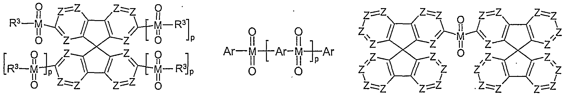
Ebenfalls bevorzugt ist ein Matrixmaterial A; welches mindestens eine Verbindung der Formel (38) oder (39) enthält,

Weiterhin bevorzugt sind anorganische Phosphoroxide und Phosphorsulfide, wie beispielsweise P4O10.Inorganic phosphorus oxides and phosphorus sulfides, such as P 4 O 10 , are also preferred.
Weiterhin bevorzugt ist ein Matrixmaterial A, welches mindestens eine 9,9'- Spirobifluoreneinheit enthält.Also preferred is a matrix material A which contains at least one 9,9'-spirobifluorene unit.
Ebenfalls bevorzugt ist ein Matrixmaterial A, welches mindestens eine Verbindung der Formel (40) bis (48) enthält,Also preferred is a matrix material A which contains at least one compound of the formulas (40) to (48),


Bedeutungen haben und für die weiteren Symbole und Indizes gilt:Have meanings and applies to the other symbols and indices:
Ar ist bei jedem Auftreten gleich oder verschieden ein mono- oder bivalentes aromatisches oder heteroaromatisches Ringsystem mit 2 bis 40 C-Atomen, vorzugsweise mit 4 bis 30 C-Atomen, wobei ein oder mehrere H-Atome durch F, Cl, Br, I ersetzt sein können und das durch einen oder mehrere, nicht-aromatische Reste R1 substituiert sein kann, wobei mehrere Substituenten R1, sowohl am selben Ring als auch an unterschiedlichen Ringen zusammen wiederum ein weiteres mono- oder polycyclisches, aliphatisches oder aromatisches Ringsystem aufspannen können; p ist bei jedem Auftreten gleich oder verschieden 0 oder 1.Ar is the same or different in each occurrence, a mono- or divalent aromatic or heteroaromatic ring system with 2 to 40 C atoms, preferably with 4 to 30 C atoms, one or more H atoms being replaced by F, Cl, Br, I. and which can be substituted by one or more non-aromatic radicals R 1 , it being possible for a plurality of substituents R 1 , both on the same ring and on different rings, to form a further mono- or polycyclic, aliphatic or aromatic ring system; p is the same or different at each occurrence 0 or 1.
Die Bevorzugung der Materialien der Formel (40) bis (48) ist insbesondere durch ihre hohen Glasübergangstemperaturen begründert. Diese liegen je nach Substitutionsmuster typischerweise über 70 °C und meist sogar oberhalb von 100 °C.The preference for the materials of the formulas (40) to (48) is in particular due to their high glass transition temperatures. Depending on the substitution pattern, these are typically above 70 ° C and usually even above 100 ° C.
Besonders bevorzugt sind Mischungen, die eines oder mehrere der oben durch Formel (1) bis (48) beschriebenen Matrixmaterialien A enthalten, dadurch gekennzeichnet, daßMixtures which contain one or more of the matrix materials A described above by formulas (1) to (48) are particularly preferred, characterized in that
L ist bei jedem Auftreten P;L is P at every occurrence;
M ist bei jedem Auftreten S;M is S at every occurrence;
X ist bei jedem Auftreten O;X is O every time it occurs;
T ist gleich oder verschieden bei jedem Auftreten B, CR1 oder P=0;T is the same or different on each occurrence B, CR 1 or P = 0;
Z ist gleich oder verschieden bei jedem Auftreten CR1 oder N;Z is the same or different on each occurrence of CR 1 or N;
R1, R2, R3 gleich oder verschieden bei jedem Auftreten CH3, CF3, -HC=CH- oder ein aromatisches oder heteroaromatisches Ringsystem mit 1 bis 40 C-Atomen, wobei ein oder mehrere H-Atome durch F, Cl, Br, I ersetzt sein können und das durch einen oder mehrere, nicht-aromatische Reste R1 substituiert sein kann, wobei mehrere Substituenten R1 miteinander ein weiteres mono- oder polycyclisches, aliphatisches oder aromatisches Ringsystem bilden können und wobei R1, R2 und/oder R3 miteinander ein mono- oder polycyclisches, aliphatisches oder aromatisches Ringsystem bilden kann; m ist 1, 2 oder 3; n ist gleich oder verschieden bei jedem Auftreten 0,1 , 2 oder 3; und wobei die Symbole I, o, R4, R5, R6, R7, R8, R9 und R10 die oben genannte Bedeutung haben.R 1 , R 2 , R 3 are the same or different with each occurrence CH 3 , CF 3 , -HC = CH- or an aromatic or heteroaromatic ring system with 1 to 40 C atoms, one or more H atoms being represented by F, Cl , Br, I can be replaced and which can be substituted by one or more non-aromatic radicals R 1 , where several substituents R 1 can form a further mono- or polycyclic, aliphatic or aromatic ring system with one another and where R 1 , R 2 and / or R 3 can form a mono- or polycyclic, aliphatic or aromatic ring system with one another; m is 1, 2 or 3; n is the same or different on each occurrence 0, 1, 2 or 3; and wherein the symbols I, o, R 4 , R 5 , R 6 , R 7 , R 8 , R 9 and R 10 have the meaning given above.
Besonders bevorzugt sind Mischungen, die eines oder mehrere der oben durch Formeln (1) bis (48) beschriebenen Matrixmaterialen A enthalten, dadurch gekennzeichnet, daß diese chiral sind.Mixtures which contain one or more of the matrix materials A described above by formulas (1) to (48) are particularly preferred, characterized in that they are chiral.
Die Verbindungen gemäß Formel (40), (41a), (42), (43), (44a), (45), (46), (47a) und (48),


Die vorliegende Erfindung wird durch die folgenden Beispiele für Matrixmaterialien A näher erläutert, ohne sie darauf einschränken zu wollen. Der Fachmann kann aus der Beschreibung und den aufgeführten Beispielen ohne erfinderisches Zutun weitere erfindungsgemäße Matrixmaterialien herstellen.The present invention is explained in more detail by the following examples of matrix materials A, without wishing to restrict it thereto. The person skilled in the art can produce further matrix materials according to the invention from the description and the examples given without inventive step.


Die oben beschriebenen erfindungsgemäßen Matrixmaterialien A, z. B. gemäß den Beispielen 50 bis 53, können beispielsweise als Co-Monomere zur Erzeugung entsprechender konjugierter, teilkonjugierter oder nicht-konjugierter Polymere oder auch als Kern von Dendrimeren, z. B. gemäß den Beispielen 54 und 55, Verwendung finden. Die entsprechende weitergehende Funktionalisierung (Polymerisation oder Umsetzung zu Dendrimeren) erfolgt dabei bevorzugt über die Halogenfunktionalität. So können die o. g. Verbindungen u. a. in lösliche Polyfluorene (z. B. gemäß EP 842208 oder WO 00/22026), Poly-spirobifluorene (z. B. gemäß EP 707020 oder EP 894107), Poly- para-phenylene (z. B. gemäß WO 92/18552), Poly-carbazole, Poly-vinylcarbazole (PVK) oder Polythiophene (z. B. gemäß EP 1028136) einpolymerisiert werden. Die oben beschriebenen konjugierten, teilkonjugierten oder nicht-konjugierten Polymere oder Dendrimere, die eine oder mehrere Struktureinheiten der Formel (1 ) bis (48) enthalten, können als Matrixmaterial in organischen Elektrolumineszenzvorrichtungen verwendet werden.The matrix materials A according to the invention described above, e.g. B. according to Examples 50 to 53, can, for example, as co-monomers to produce appropriate conjugated, partially conjugated or non-conjugated polymers or as the core of dendrimers, for. B. according to Examples 54 and 55, use. The corresponding further functionalization (polymerization or conversion to dendrimers) is preferably carried out via the halogen functionality. For example, the above-mentioned compounds can be converted into soluble polyfluorenes (e.g. according to EP 842208 or WO 00/22026), poly-spirobifluorenes (e.g. according to EP 707020 or EP 894107), poly-para-phenylenes (e.g. according to WO 92/18552), poly-carbazoles, poly-vinylcarbazoles (PVK) or polythiophenes (e.g. according to EP 1028136). The conjugated, partially conjugated or non-conjugated polymers or dendrimers described above, which contain one or more structural units of the formulas (1) to (48), can be used as matrix material in organic electroluminescent devices.
Weiterhin können die erfindungsgemäßen Matrixmaterialien A auch durch die beispielsweise o. g. Reaktionstypen weiter funktionalisiert werden und so zu erweiterten Mat xmate alien A umgesetzt werden. Hier ist als Beispiel die Funktionalisierung mit Arylboronsäuren gemäß SUZUKI oder mit Aminen gemäß HARTWIG-BUCHWALD zu nennen.Furthermore, the matrix materials A according to the invention can also be obtained, for example, from Reaction types can be further functionalized and thus converted into expanded Mat xmate alien A. The functionalization with arylboronic acids according to SUZUKI or with amines according to HARTWIG-BUCHWALD can be mentioned here as an example.
Um als Funktionsmaterial Verwendung zu finden, werden die erfindungsgemäßen Matrixmaterialien A oder deren Mischungen oder die Matrixmaterialien A enthaltende Polymere oder Dendrimere oder deren Mischungen oder Mischungen aus den Matrixmaterialien A und den Matrixmaterialien A enthaltenden Polymeren oder Dendrimeren, gegebenenfalls zusammen mit den Emittern B, nach allgemein bekannten, dem Fachmann geläufigen Methoden, wie Vakuumverdampfung, Verdampfen im Trägergasstrom oder auch aus Lösung durch Spincoaten oder mit verschiedenen Druckverfahren (z. B. Tintenstrahldrucken, Off-set-Drucken, LITI-Druck, etc.), in Form eines Films auf ein Substrat aufgebracht.In order to be used as functional material, the matrix materials A according to the invention or their mixtures or the polymers or dendrimers containing the matrix materials A or their mixtures or mixtures of the polymers or dendrimers containing the matrix materials A and the matrix materials A, optionally together with the emitters B, generally known methods known to those skilled in the art, such as vacuum evaporation, evaporation in a carrier gas stream or also from solution by spin coating or with various printing processes (for example ink-jet printing, offset printing, LITI printing, etc.) in the form of a film Applied substrate.
Dabei kann die Verwendung von Druckverfahren Vorteile hinsichtlich der Skalierbarkeit der Fertigung, als auch bezüglich der Einstellung von Mischungsverhältnissen in verwendeten Blend-Schichten haben.The use of printing processes can have advantages with regard to the scalability of the production and also with regard to the setting of mixing ratios in the blend layers used.
Die oben beschriebenen Matrixmaterialien werden in Kombination mit Phosphoreszenz- Emittern verwendet. Die so dargestellten organischen Elektrolumineszenzvorrichtungen zeichnen sich dadurch aus, daß sie als Emitter B mindestens eine Verbindung enthalten, die dadurch gekennzeichnet ist, daß sie bei geeigneter Anregung Licht, vorzugsweise im sichtbaren Bereich, emittiert und außerdem mindestens ein Atom der Ordungszahl größer 20, bevorzugt größer 38 und kleiner 84, besonders bevorzugt größer 56 und kleiner 80 enthält.The matrix materials described above are used in combination with phosphorescence emitters. The organic electroluminescent devices represented in this way are distinguished by the fact that they contain at least one compound as emitter B, which is characterized in that, with suitable excitation, it emits light, preferably in the visible range, and also at least one atom of atomic number greater than 20, preferably greater 38 and less than 84, particularly preferably greater than 56 and less than 80.
Bevorzugt werden als Phosphoreszenz-Emitter in den oben beschriebenen organischen Elektroluminesenzvόrrichtungen Verbindungen, die Molybdän, Wolfram, Rhenium, Ruthenium, Osmium, Rhodium, Iridium, Palladium, Platin, Silber, Gold oder Europium enthalten, verwendet.Compounds which contain molybdenum, tungsten, rhenium, ruthenium, osmium, rhodium, iridium, palladium, platinum, silver, gold or europium are preferably used as phosphorescence emitters in the organic electroluminescent devices described above.
Besonders bevorzugte Mischungen enthalten als Emitter B mindestens eine Verbindung der Formel (49) bis (52),


DCy ist gleich oder verschieden bei jedem Auftreten eine cyclische Gruppe, die mindestens ein Donoratom, bevorzugt Stickstoff oder Phosphor, enthält, über welches die cyclische Gruppe an das Metall gebunden ist, und die wiederum einen oder mehrere Substituenten R11 tragen kann; die Gruppen DCy und CCy sind über eine kovalente Bindung miteinander verbunden;DCy is the same or different with each occurrence a cyclic group which contains at least one donor atom, preferably nitrogen or phosphorus, via which the cyclic group is bonded to the metal and which in turn can carry one or more substituents R 11 ; the groups DCy and CCy are connected to one another via a covalent bond;
CCy ist gleich oder verschieden bei jedem Auftreten eine cyclische Gruppe, die ein Kohlenstoffatom enthält, über welches die cyclische Gruppe an das Metall gebunden ist und die wiederum einen oder mehrere Substituenten R11 tragen kann;CCy is the same or different with each occurrence a cyclic group which contains a carbon atom via which the cyclic group is bonded to the metal and which in turn can carry one or more substituents R 11 ;
R 11 ist gleich oder verschieden bei jedem Auftreten H, F, Cl, Br, I, NO2, CN, eine geradkettige, verzweigte oder cyclische Alkyl- oder Alkoxygruppe mit 1 bis 40 C-Atomen, wobei ein oder mehrere nicht benachbarte CH2-Gruppen durch C=O, C=S, C=Se, C=NR4, -O-, -S-, -NR5- oder -CONR6- ersetzt sein können und wobei ein oder mehrere H-Atome durch F ersetzt sein können, oder ein aromatisches oder heteroaromatisches Ringsystem mit 4 bis 14 C-Atomen, das durch einen oder mehrere, nicht-aromatische Reste R11 substituiert sein kann, wobei mehrere Substituenten R11, sowohl am selben Ring als auch an den beiden unterschiedlichen Ringen zusammen wiederum ein weiteres mono- oder polycyclisches Ringsystem aufspannen können; ist gleich oder verschieden bei jedem Auftreten ein zweizähnig chelatisierender Ligand, bevorzugt ein Di-ketonat-ligand;R 11 is the same or different with each occurrence H, F, Cl, Br, I, NO 2 , CN, a straight-chain, branched or cyclic alkyl or alkoxy group with 1 to 40 C atoms, one or more non-adjacent CH 2 Groups can be replaced by C = O, C = S, C = Se, C = NR 4 , -O-, -S-, -NR 5 - or -CONR 6 - and one or more H atoms can be replaced by F can be replaced, or an aromatic or heteroaromatic ring system with 4 to 14 carbon atoms, which can be substituted by one or more, non-aromatic radicals R 11 , wherein several substituents R 11 , both on the same ring and on the two different Rings together can in turn span another mono- or polycyclic ring system; is the same or different at each occurrence a bidentate chelating ligand, preferably a dicetonate ligand;
R4, R5, R6 ist gleich oder verschieden bei jedem Auftreten H oder ein aliphatischer oder aromatischer Kohlenwasserstoffrest mit 1 bis 20 C-Atomen.R 4 , R 5 , R 6 are the same or different with each occurrence H or an aliphatic or aromatic hydrocarbon radical with 1 to 20 C atoms.
Beispiele der oben beschriebenen Emitter können zum Beispiel den Anmeldungen WO 00/70655, WO 01/41512, WO 02/02714, WO 02/15645, EP 1191613, EP 1191612 und EP 1191614 entnommen werden; diese werden hiermit via Zitat als Bestandteil der Anmeldung betrachtet.Examples of the emitters described above can be found, for example, in applications WO 00/70655, WO 01/41512, WO 02/02714, WO 02/15645, EP 1191613, EP 1191612 and EP 1191614; these are hereby considered as part of the registration via quotation.
Die erfindungsgemäße Mischung enthält zwischen 1 und 99 Gew.%, vorzugsweise zwischen 3 und 95 Gew.%, besonders bevorzugt zwischen 5 und 50 Gew.%, insbesondere zwischen 7 und 20 Gew.% Emitter B bezogen auf die Gesamtmischung aus Emitter B und Matrixmaterial A.The mixture according to the invention contains between 1 and 99% by weight, preferably between 3 and 95% by weight, particularly preferably between 5 and 50% by weight, in particular between 7 and 20% by weight of emitter B based on the total mixture of emitter B and matrix material A.
Weiterer Gegenstand der vorliegenden Erfindung sind elektronische Bauteile, insbesondere organische Elektrolumineszenzvorrichtungen (OLED), organische Solarzellen (O-SCs), organische Feldeffekttransistoren (O-FETs), organische optische Detektoren, organische Photorezeptoren in der Elektrophotographie oder auch organische Laserdioden (O-Laser) enthaltend die erfindungsgemäße Mischung aus Matrixmaterial A und Emissionsmaterial B.The present invention further relates to electronic components, in particular organic electroluminescent devices (OLED), organic solar cells (O-SCs), organic field-effect transistors (O-FETs), organic optical detectors, organic photoreceptors in electrophotography or organic laser diodes (O-lasers). containing the mixture of matrix material A and emission material B according to the invention
Besonders bevorzugt sind organische Elektrolumineszenzvorrichtungen, die mindestens eine emittierende Schicht (EML) aufweist, enthaltend eine Mischung aus mindestens einemOrganic electroluminescent devices which have at least one emitting layer (EML) containing a mixture of at least one are particularly preferred
Matrixmaterial A und mindestens einem zur Emission befähigten Emissionsmaterial B, wobei,Matrix material A and at least one emission material B capable of emission,
A eine Verbindung ist, welche mindestens eine Struktureinheit der Form Q=X enthält, dadurch gekennzeichnet, daß X mindestens ein nicht-bindendes Elektronenpaar aufweist und gegebenenfalls auch glasartige Schichten bilden kann, und wobei Q P, As, Sb, Bi, S, Se oder Te ist undA is a compound which contains at least one structural unit of the form Q = X, characterized in that X has at least one non-binding pair of electrons and can optionally also form glass-like layers, and where QP, As, Sb, Bi, S, Se or Te is and
B eine Verbindung ist, dadurch gekennzeichnet, daß sie bei geeigneter Anregung Licht emittiert und welche mindestens ein Element der Ordungszahl größer 20 enthält.B is a compound, characterized in that it emits light with suitable excitation and which contains at least one element of an atomic number greater than 20.
Bevorzugt werden organische Elektrolumineszenzvorrichtungen, die eine emittierende Schicht (EML) enthalten, enthaltend eine Mischung aus mindestens einem Matrixmaterial A und mindestens einem zur Emission befähigten Emissionsmaterial B, wobei A eine Verbindung ist, welche mindestens eine Struktureinheit der Form Q=X enthält, dadurch gekennzeichnet, daß X mindestens ein nicht-bindendes Elektronenpaar aufweist, und die Glastemperatur Tg der Substanz A größer 70 °C ist, und B eine Verbindung ist, dadurch gekennzeichnet, daß sie bei geeigneter Anregung Licht emittiert und welche mindestens ein Element der Ordungszahl größer 20 enthält, und Q die oben angegebene Bedeutung hat.Organic electroluminescent devices which contain an emitting layer (EML) are preferred, comprising a mixture of at least one matrix material A and at least one emission material B capable of emission, wherein A is a compound which contains at least one structural unit of the form Q = X that X has at least one non-binding pair of electrons, and the glass transition temperature T g of substance A is greater than 70 ° C, and B is a compound, characterized in that it emits light with suitable excitation and which has at least one element of the atomic number greater than 20 contains, and Q has the meaning given above.
Die organische Elektrolumineszenzvorrichtung kann außer der Kathode, der Anode und der Emitterschicht weitere Schichten enthalten, wie z. B. Lochinjektionsschicht, Lochtransportschicht, Lochblockierschicht, Elektronentransportschicht und/oder Elektroneninjektionsschicht. Es sei aber an dieser Stelle darauf hingewiesen, daß nicht notwendigerweise jede dieser Schichten vorhanden sein muß. So hat sich beispielsweise gezeigt, daß eine OLED, die weder eine separate Lochblockierschicht, noch eine separate Elektronentransportschicht enthält, weiterhin sehr gute Ergebnisse in der Elektrolumineszenz zeigt, insbesondere eine nochmals deutlich höhere Leistungseffizienz. Dies ist besonders überraschend, da eine entsprechende OLED mit einem Carbazol- haltigen Matrixmaterial ohne Lochblockier- und Elektronentransportschicht nur sehr geringe Leistungseffizienzen zeigt, insbesondere bei hoher Helligkeit (vgl. Adachi et al., Organic Electronics 2001 , 2, 37).In addition to the cathode, the anode and the emitter layer, the organic electroluminescent device can contain further layers, such as, for. B. hole injection layer, hole transport layer, hole blocking layer, electron transport layer and / or electron injection layer. At this point, however, it should be pointed out that each of these layers does not necessarily have to be present. It has been shown, for example, that an OLED which neither contains a separate hole blocking layer nor a separate electron transport layer continues to show very good results in electroluminescence, in particular a significantly higher power efficiency. This is particularly surprising since a corresponding OLED with a carbazole-containing matrix material without a hole blocking and electron transport layer shows only very low performance efficiencies, in particular at high brightness (cf. Adachi et al., Organic Electronics 2001, 2, 37).
Ein weiterer Gegenstand der Erfindung ist also eine organische Elektrolumineszenzvorrichtung, enthaltend eine erfindungsgemäße Mischung, die ohne Verwendung einer Lochblockierschicht direkt an die Elektronentransportschicht grenzt oder die ohne Verwendung einer Lochblockierschicht und einer Elektronentransportschicht direkt an die Elektroneninjektionsschicht oder an die Kathode grenzt.Another object of the invention is therefore an organic electroluminescent device containing a mixture according to the invention which directly adjoins the electron transport layer without using a hole blocking layer or which directly adjoins the electron injection layer or the cathode without using a hole blocking layer and an electron transport layer.
Die organischen Elektrolumineszenzvorrichtungen zeigen höhere Effizienz, deutlich längere Lebensdauer und, insbesondere ohne Verwendung einer Lochblockier- und Elektronentransportschicht, deutlich niedrigere Betriebsspannungen und höhere Leistungseffizienzen als OLEDs gemäß dem Stand der Technik, die CBP als Matrixmaterial verwenden. Durch Weglassen der Lochblockier- und Elektronentransportschichten vereinfacht sich weiterhin der Aufbau der OLED, was einen erheblichen technologischen Vorteil darstellt.The organic electroluminescent devices show higher efficiency, significantly longer life and, in particular without using a hole blocking and electron transport layer, significantly lower operating voltages and higher power efficiencies than OLEDs according to the prior art, which use CBP as the matrix material. By omitting the hole blocking and electron transport layers, the structure of the OLED is further simplified, which represents a considerable technological advantage.
Die bevorzugten Ausführungsformen der erfindungsgemäßen Mischungen aus Matrixmaterial A und Emissionsmaterial B sind auch für die erfindungsgemäßen elektronischen Bauteile, insbesondere für die organischen Elektrolumineszenzvorrichtungen (OLED), organischen Solarzellen (O-SCs), organischen Feldeffekttransistoren (O-FETs), organische optische Detektoren, organische Photorezeptoren für die Elektrophotographie öder auch organischen Laserdioden (O-Laser) gegeben. Zur Vermeidung von unnötigen Wiederholungen wird daher auf erneute Aufzählung an dieser Stelle verzichtet.The preferred embodiments of the mixtures of matrix material A and emission material B according to the invention are also for the electronic components according to the invention, in particular for the organic electroluminescent devices (OLED), organic solar cells (O-SCs), organic field effect transistors (O-FETs), organic optical detectors, organic Photoreceptors for electrophotography or organic laser diodes (O-lasers). To avoid unnecessary repetitions, we do not list them again here.
Im vorliegenden Anmeldetext und auch in den im weiteren folgenden Beispielen wird nur auf organische Leuchtdioden und die entsprechenden Displays abgezielt. Trotz dieser Beschränkung der Beschreibung ist es für den Fachmann ohne weiteres erfinderisches Zutun möglich, entsprechende erfindungsgemäße Schichten aus den erfindungsgemäßen Mischungen herzustellen und anzuwenden, insbesondere in OLED-nahen oder verwandten Anwendungen.In the present application text and also in the following examples, only organic light-emitting diodes and the corresponding displays are targeted. Despite this limitation of the description, it is possible for the person skilled in the art without further inventive step to produce and use corresponding layers according to the invention from the mixtures according to the invention, in particular in OLED-related or related applications.
Die nachfolgend beschriebenen Beispiele zeigen klar auf, daß die erfindungsgemäßen Matrixmaterialien A zu einer deutlichen Verbesserung der Effizienz und der Lebendauer der mit diesen hergestellten Elektrolumineszenzvorrichtungen führen. Außerdem gelingt es bei Verwendung der Matrixmaterialien A, blau emittierende Elektrolumineszenzvorrichtungen herzustellen.The examples described below clearly show that the matrix materials A according to the invention lead to a significant improvement in the efficiency and the lifespan of the electroluminescent devices produced with them. In addition, the matrix materials A can be used to produce blue-emitting electroluminescent devices.
Beispiele:Examples:
Allgemeines Meßverfahren zur Bestimmung der Glasübungstemperatur: Die subiimierten Proben wurden zunächst mit einer Heizrate von 10 K/min. ausgehend von 25 °C bis zum Schmelzpunkt der Substanz +50 K aufgeheizt. Anschließend wurden sie von dieser Temperatur mit einer Heizrate von 80 K/min auf 25 °C abgekühlt. Die Messung der Glasübergangstemperatur Tg erfolgte durch erneutes Aufheizen mit einer Heizrate von 10 K/min bis zu einer Temperatur 50 K oberhalb des Schmelzpunktes der Substanz mit einem Gerät der Fa. Netzsch DCS 204 (TASC 414/4 Controler und CC200 C Controler).General measuring method for determining the glass exercise temperature: The sublimated samples were first at a heating rate of 10 K / min. heated from 25 ° C to the melting point of the substance +50 K. They were then cooled to 25 ° C. from this temperature at a heating rate of 80 K / min. The glass transition temperature T g was measured by reheating at a heating rate of 10 K / min to a temperature of 50 K above the melting point of the substance using a device from Netzsch DCS 204 (TASC 414/4 Controler and CC200 C Controler).
1. Synthese von Matrixmaterialien1. Synthesis of matrix materials
Die nachfolgenden Synthesen wurden - sofern nicht anders angegeben - unter einer Schutzgasatmosphäre in getrockneten Lösemitteln durchgeführt. Die Edukte wurden von ALDRICH [Dichlorphenylphosphin] bezogen. 2-Brom-9,9'-spirobifluoren wurde nach Literaturmethoden (Pei, Jian et al., J. Org. Chem., 2002, 67(14), 4924-4936) dargestellt.Unless otherwise stated, the following syntheses were carried out under an inert gas atmosphere in dried solvents. The starting materials were obtained from ALDRICH [dichlorophenylphosphine]. 2-bromo-9,9-spirobifluorene was' according to literature methods (Pei, Jian et al., J. Org. Chem., 2002, 67 (14), 4924-4936), respectively.
Beispiel 1 : Bis(9,9'-spiro-bifluoren-2-yl)phenylphosphinoxid (Matrixmaterial M1)Example 1: Bis (9,9'-spirobifluoren-2-yl) phenylphosphine oxide (matrix material M1)
Aus einer Lösung von 98.8 g (250 mmol) 2-Brom-9,9'-spirobifluoren und 6 mlSpirobifluorene from a solution of 98.8 g (250 mmol) 2-bromo-9,9 ', and 6 ml
1 ,2-Dichlorethan in 1000 ml THF und 7.1 g (290 mmol) Magnesium wurde in der Siedehitze das entsprechende Grignard-Reagens hergestellt. Zu dieser Grignard-Lösung wurde bei1, 2-dichloroethane in 1000 ml THF and 7.1 g (290 mmol) magnesium the corresponding Grignard reagent was produced at the boiling point. This Grignard solution was added to
0-5 °C eine Lösung von 16.3 ml (120 mmol) Dichlorphenylphosphin in 100 ml THF während0-5 ° C a solution of 16.3 ml (120 mmol) dichlorophenylphosphine in 100 ml THF during
15 min. zugetropft. Anschließend wurde die Mischung 1 h unter Rückfluß erhitzt. Nach15 minutes. dropwise. The mixture was then heated under reflux for 1 h. To
Abkühlen wurde die Mischung mit 10 ml Wasser versetzt und bis zur Trockene eingeengt.After cooling, the mixture was mixed with 10 ml of water and concentrated to dryness.
Der farblose Rückstand wurde in 1000 ml Dichlormethan aufgenommen, die Suspension wurde dreimal mit 300 ml Wasser gewaschen. Die organische Phase wurde abgetrennt, über Natriumsulfat getrocknet und anschließend eingeengt. Der farblose Rückstand wurde in 1000 ml Essigsäureethylester gelöst und tropfenweise unter gutem Rühren mit einemThe colorless residue was taken up in 1000 ml of dichloromethane, the suspension was washed three times with 300 ml of water. The organic phase was separated off, dried over sodium sulfate and then concentrated. The colorless residue was dissolved in 1000 ml of ethyl acetate and added dropwise with good stirring using a
Gemisch aus 10.3 ml Wasserstoffperoxid (35 Gew.% in Wasser) und 100 ml Wasser versetzt. Nach 18 h Rühren wurde der ausgefallene farblose Feststoff abgesaugt, mitMixture of 10.3 ml of hydrogen peroxide (35% by weight in water) and 100 ml of water are added. After stirring for 18 h, the colorless solid which had precipitated was filtered off with
Ethanol gewaschen und getrocknet. Der Feststoff wurde dreimal aus Chlorbenzol (10 ml/g) umkristallisiert und anschließend im Hochvakuum (T = 385 °C, p = 5 x 10"5 mbar) sublimiert.Washed and dried ethanol. The solid was recrystallized three times from chlorobenzene (10 ml / g) and then sublimed in a high vacuum (T = 385 ° C, p = 5 x 10 "5 mbar).
Die Ausbeute bei einer Reinheit > 99.9 % nach HPLC betrug 40.1 g (53 mmol), entsprechend 42.4 % der Th.The yield with a purity> 99.9% according to HPLC was 40.1 g (53 mmol), corresponding to 42.4% of th.
Schmelzpunkt: Tm = 334 °C , Glasübergangspunkt: Tg = 161 °C.Melting point: T m = 334 ° C, glass transition point: T g = 161 ° C.
31P-NMR (CDCI3): D [ppm] = 30.4 (s). 31 P NMR (CDCI 3 ): D [ppm] = 30.4 (s).
1H-NMR (CDCI3): D [ppm] = 7.83 - 7.81 (m, 2 H), 7.76 - 7.75 (m, 6 H), 7.38 - 7.22 (m, 1 H-NMR (CDCI 3 ): D [ppm] = 7.83 - 7.81 (m, 2 H), 7.76 - 7.75 (m, 6 H), 7.38 - 7.22 (m,
15 H), 7.15 - 7.12 (m, 2 H), 7.06 - 7.03 (m, 4 H), 6.72 - 6.71 (m, 2 H), 6.64 - 6.60 (m, 4 H).15 H), 7.15 - 7.12 (m, 2 H), 7.06 - 7.03 (m, 4 H), 6.72 - 6.71 (m, 2 H), 6.64 - 6.60 (m, 4 H).
Beispiel 2: Bis(9,9'-spirobifluoren-2-yl)sulfoxid (Matrixmaterial M2)Example 2: Bis (9,9 'spirobifluorene-2-yl) sulfoxide (matrix material M2)
Zu einer auf -78 °C gekühlten Suspension von 98.8 g (250 mmol) 2-Brom-9,9'- spirobifluoren in 1500 ml THF wurden 110 ml (275 mmol) einer n-Butyllithium-Lösung (2.5 M in Hexan) so zugetropft, daß die Temperatur nicht über -65 °C anstieg. Die Reaktionsmischung wurde 3 h bei -78 °C gerührt und dann mit einem Gemisch aus 7.2 ml (125 mmol) Thionylchlorid und 300 ml THF tropfenweise versetzt und anschließend noch weitere 3 h bei -78 °C nachgerührt. Nach Erwärmen der Reaktionsmischung auf Raumtemperatur wurde das Reaktionsgemisch mit 25 ml Wasser versetzt und im Vakuum zur Trockene eingeengt. Der Rückstand wurde in 1000 ml Dioxan und 500 ml Wasser aufgenommen, die organische Phase wurde abgetrennt, nochmals mit 500 ml Wasser gewaschen und anschließend über Magnesiumsulfat getrocknet. Anschließend wurde der nach Einengen der organischen Phase verbliebene Feststoff fünfmal aus Dioxan (1 g/ml) umkristallisiert und dann im Hochvakuum (T = 370 °C, p = 5 x 10~5 mbar) sublimiert. DieTo a cooled -78 ° C suspension of 98.8 g (250 mmol) 2-bromo-9,9 '- spirobifluorene in 1500 ml THF was added 110 ml (275 mmol) of an n-butyllithium solution (2.5 M in hexane) so added dropwise that the temperature did not rise above -65 ° C. The reaction mixture was stirred at -78 ° C. for 3 h and then a mixture of 7.2 ml (125 mmol) of thionyl chloride and 300 ml of THF was added dropwise and the mixture was then stirred at -78 ° C. for a further 3 h. After warming up the reaction mixture At room temperature, the reaction mixture was mixed with 25 ml of water and concentrated to dryness in vacuo. The residue was taken up in 1000 ml of dioxane and 500 ml of water, the organic phase was separated off, washed again with 500 ml of water and then dried over magnesium sulfate. The solid which remained after concentration of the organic phase was then recrystallized five times from dioxane (1 g / ml) and then sublimed in a high vacuum (T = 370 ° C., p = 5 × 10 -5 mbar). The
Ausbeute bei einer Reinheit > 99.9 % nach HPLC betrug 114.0 g (168 mmol), entsprechendYield with a purity> 99.9% according to HPLC was 114.0 g (168 mmol), correspondingly
67.2 % der Th..67.2% of th ..
Schmelzpunkt: Tm = 365 °C , Glasübergangspunkt: Tg = 178 °C.Melting point: T m = 365 ° C, glass transition point: T g = 178 ° C.
1H-NMR (CDCI3): G [ppm] = 7.83 (m, 4H), 7.75 (m, 2H), 7.73 (m, 2H), 7.37-7.29 1 H NMR (CDCI 3 ): G [ppm] = 7.83 (m, 4H), 7.75 (m, 2H), 7.73 (m, 2H), 7.37-7.29
(br. m, 8H), 7.09-7.03 (br. m, 6H), 6.86 (m, 2H), 6.70 (m, 4H), 6.65 (m, 2H).(br. m, 8H), 7.09-7.03 (br. m, 6H), 6.86 (m, 2H), 6.70 (m, 4H), 6.65 (m, 2H).
Beispiel 3: 1,1'-Binaphthyl-2,2'-bis(diphenylphosphinoxid) (Matrixmaterial M3)Example 3: 1,1'-binaphthyl-2,2'-bis (diphenylphosphine oxide) (matrix material M3)
Die Synthese wurde durch Oxidation von racemischem 1 ,1 '-Binaphthyl-2,2'- bis(diphenylphosphin) (erhalten von Aldrich) mit Wasserstoffperoxid in Analogie zu Beispiel 1 durchgeführt.The synthesis was carried out by oxidation of racemic 1, 1'-binaphthyl-2,2'-bis (diphenylphosphine) (obtained from Aldrich) with hydrogen peroxide in analogy to Example 1.
Die Matrixmaterialien M1 bis M3 sind der Übersichtlichkeit halber im folgenden nochmals abgebildet:For the sake of clarity, the matrix materials M1 to M3 are shown again below:


2. Herstellung und Charakterisierung von organischen Elektrolumineszenz- vorrichtungen, die erfindungsgemäße Verbindungen enthalten2. Production and Characterization of Organic Electroluminescent Devices Containing Compounds According to the Invention
Die Herstellung von OLEDs erfolgte nach dem im folgenden skizzierten allgemeinen Verfahren. Dieses mußte natürlich im Einzelfall auf die jeweiligen Gegebenheiten (z. B. Schichtdickenvariation, um optimale Effizienz bzw. Farbe zu erreichen) angepaßt werden. Erfindungsgemäße Elektrolumineszenzvorrichtungen können beispielsweise wie in der nicht offengelegten Anmeldung DE 10317556.3 beschrieben, dargestellt werden. 3. Device-BeispieleOLEDs were produced using the general process outlined below. In individual cases, of course, this had to be adapted to the respective circumstances (e.g. layer thickness variation in order to achieve optimum efficiency or color). Electroluminescent devices according to the invention can be represented, for example, as described in the unpublished application DE 10317556.3. 3. Device examples
In diesen Beispielen werden die Ergebnisse verschiedener OLEDs gegenübergestellt. Der grundlegende Aufbau, die verwendeten Materialien, der Dotierungsgrad und die Schichtdicken war für die Beispielexperimente zur besseren Vergleichbarkeit identisch. Es wurde lediglich das Wirtsmaterial in der Emitterschicht getauscht.In these examples the results of different OLEDs are compared. The basic structure, the materials used, the degree of doping and the layer thicknesses were identical for the example experiments for better comparability. Only the host material in the emitter layer was exchanged.
Das erste Beispiel beschreibt einen Vergleichsstandard gemäß dem Stand der Technik, bei dem die Emitterschicht aus dem Wirtsmaterial CBP und dem Gastmaterial lr(PPy)3 besteht. Des weiteren wird eine OLED mit einer Emitterschicht bestehend aus dem Wirtsmaterial Bis(9,9'-spirobifluoren-2-yl)phenylphosphinoxid (Synthese s. Beispiel 1 ) und dem Gastmaterial lr(PPy)3 (synthetisiert nach WO 02/060910) beschrieben, ebenso wie OLEDs mit weiteren erfindungsgemäßen Wirtsmaterialien. Es wurden OLEDs mit folgendem Aufbau erzeugt:The first example describes a comparison standard according to the prior art, in which the emitter layer consists of the host material CBP and the guest material lr (PPy) 3 . Furthermore, an OLED with an emitter layer consisting of the host material bis (9,9'-spirobifluoren-2-yl) phenylphosphine oxide (synthesis see example 1) and the guest material lr (PPy) 3 (synthesized according to WO 02/060910) is described , as well as OLEDs with other host materials according to the invention. OLEDs with the following structure were produced:
PEDOT 60 nm (aus Wasser aufgeschleudert; PEDOT bezogen von H. C. Starck; Poly[3,4-ethylendioxy-2,5-thiophen])PEDOT 60 nm (spun on water; PEDOT obtained from H.C. Starck; poly [3,4-ethylenedioxy-2,5-thiophene])
NaphDATA 20 nm (aufgedampft; NaphDATA bezogen von SynTec; 4,4',4"-Tris(N- 1-naphthyl-N-phenyl-amino)-triphenylaminNaphDATA 20 nm (evaporated; NaphDATA purchased from SynTec; 4,4 ', 4 "-Tris (N-1-naphthyl-N-phenylamino) -triphenylamine
S-TAD 20 nm (aufgedampft; S-TAD hergestellt nach WO99/12888; 2,2', 7,7'- Tetrakis(diphenylamino)-spirobifluoren)S-TAD 20 nm (evaporated; S-TAD manufactured according to WO99 / 12888; 2,2 ', 7,7'-tetrakis (diphenylamino) -spirobifluorene)
Emitter-Schicht: CPB 20 nm (aufgedampft; CPB bezogen von ALDRICH und weiter gereinigt, schließlich noch zweimal sublimiert; 4,4'-Bis-(N-carbazolyl)biphenyl) Vergleichsstandard)Emitter layer: CPB 20 nm (evaporated; CPB obtained from ALDRICH and further purified, finally sublimed twice; 4,4'-bis (N-carbazolyl) biphenyl) comparison standard)
ODER:OR:
Bis(9,9'-spiro- bifluoren-2-yl)- phenylphos- phinoxid 20 nm (aufgedampft; synthetisiert und gereinigt nach Beispiel 1)Bis (9,9 '-spiro- bifluoren-2-yl) - phenylphos- phosphine oxide 20 nm (vapor-deposited; synthesized and purified according to Example 1)
ODER:OR:
Bis(9,9'-spiro- bifluoren-2-yl)- sulfoxid 20 nm (aufgedampft; synthetisiert und gereinigt nach Beispiel 2)Bis (9,9'-spirobifluoren-2-yl) sulfoxide 20 nm (evaporated; synthesized and purified according to Example 2)
ODER:OR:
1 ,1'-Binaphthyl-1, 1'-binaphthyl
2,2'-bis(diphenyl- phosphinoxid) 20 nm (aufgedampft; synthetisiert und gereinigt nach Beispiel 3); jeweils dotiert mit 15 %Triplett-Emitter: lr(PPy)3 (aufgedampft; synthetisiert nach WO 02/060910)2,2'-bis (diphenylphosphine oxide) 20 nm (evaporated; synthesized and purified according to Example 3); each doped with 15% triplet emitter: lr (PPy) 3 (evaporated; synthesized according to WO 02/060910)
BCP 10 nm (aufgedampft; BCP bezogen von ABCR, verwendet wie erhalten; 2,9-Dimethyl-4,7-diphenyl-1 ,10-phenanthrolin); nicht in allen Beispielen verwendet; A1Q3 10 nm (aufgedampft: AIQ3 bezogen von SynTec; Ths(chinolinolato)aluminium(lll)); nicht in allen Beispielen verwendet Ba-Al 3 nm Ba, darauf 150 nm AI als Kathode.BCP 10 nm (evaporated; BCP obtained from ABCR, used as received; 2,9-dimethyl-4,7-diphenyl-1, 10-phenanthroline); not used in all examples; A1Q 3 10 nm (evaporated: AIQ 3 purchased from SynTec; Ths (quinolinolato) aluminum (III)); Ba-Al does not use 3 nm Ba in all of the examples, 150 nm Al as cathode thereon.
Diese noch nicht optimierten OLEDs wurden standardmäßig charakterisiert; hierfür wurden die Elektrolumineszenzspektren, die Effizienz (gemessen in cd/A) in Abhängigkeit von der Helligkeit, berechnet aus Strom-Spannungs-Helligkeit-Kennlinien (lUL-Kennlinien), und die Lebensdauer bestimmt.These OLEDs, which have not yet been optimized, have been characterized as standard; For this, the electroluminescence spectra, the efficiency (measured in cd / A) depending on the brightness, calculated from current-voltage-brightness characteristics (IUL characteristics), and the service life were determined.
Elektrolumineszenzspektren:electroluminescence:
Die OLEDs, sowohl der Vergleichsstandard (OLED mit CBP), als auch die OLEDs mit Bis(9,9'-spirobifluoren-2-yl)phenylphosphinoxid, mit Bis(9,9'-spirobifluoren-2-yl)sulfoxid und mit 1 ,1 '-Binaphthyl-2,2'-bis(diphenylphosphinoxid) als Wirtsmaterial zeigen grüne Emission, resultierend aus dem Dotanden lr(PPy)3.The OLEDs, both the reference standard (OLED with CBP), as well as the OLEDs with bis (9,9 'spirobifluorene-2-yl) phenylphosphine, with bis (9,9' spirobifluorene-2-yl) sulfoxide and treated with 1 , 1 '-Binaphthyl-2,2'-bis (diphenylphosphine oxide) as host material show green emission, resulting from the dopant lr (PPy) 3 .
Effizienz als Funktion der Helligkeit:Efficiency as a function of brightness:
Für OLEDs hergestellt mit dem Wirtsmaterial CBP (Tabelle 1 , Beispiel 1 ) erhält man, unter den oben beschriebenen Bedingungen, typischerweise eine Effizienz von etwa 20 bis 25 cd/A, und für die Referenzleuchtdichte von 100 cd/m2 werden 4.8 V benötigt. Im Gegensatz dazu zeigen OLEDs hergestellt mit dem Wirtsmaterial Bis(9,9'-spirobifluoren- . 2-yl)phenylphosphinoxid eine maximale Effizienz von über 40 cd/A, wobei die benötigte Spannung für die Referenzleuchtdichte von 100 cd/m2 sogar auf 4.0 V gesenkt wird (Fig.1 und Tabelle 1 , Beispiel 2a).For OLEDs produced with the host material CBP (Table 1, Example 1), an efficiency of approximately 20 to 25 cd / A is typically obtained under the conditions described above, and 4.8 V are required for the reference luminance of 100 cd / m 2 . In contrast, OLEDs produced with the host material bis (9,9 -spirobifluoren- '. 2-yl) phenylphosphine a maximum efficiency of about 40 cd / A, where the required voltage for the reference luminance of 100 cd / m 2 even 4.0 V is reduced (Fig. 1 and Table 1, Example 2a).
Insbesondere wenn weder eine Lochblockierschicht (HBL), noch eine Elektronentransportschicht (ETL) verwendet werden, wenn also die dotierte Matrix (EML) an die Kathode bzw. die Elektroneninjektionsschicht grenzt, werden besonders hohe Leistungseffizienzen (gemessen in Im/W) erreicht, wie in Fig. 2 abgebildet (siehe auch Tabelle 1 , Beispiel 2a). So wird beim Vergleichsstandard (unter Verwendung von BCP als Lochblockierschicht und AIQ3 als Elektronentransportschicht) eine maximale Leistungseffizienz von 12 ImΛ/V erreicht. Mit Bis(9,9'-spirobifluoren-2-yl)phenylphosphinoxid wird, ebenfalls unter Verwendung von BCP und AIQ3, eine maximale Leistungseffizienz von 34 ImΛ/V erreicht, während ohne Verwendung von BCP und AIQ3, d. h. wenn die dotierte Matrix (EML) direkt an die Kathode angrenzt, eine maximale Leistungseffizienz von 42 Im/W erreicht wird (Tabelle 1 , Beispiel 2b). Bei einer Helligkeit von 100 cd/m2 ist die Leistungseffizienz immer noch 16 ImΛ/V (mit Verwendung einer HBL und einer ETL) und 25 Im/W, wenn die dotierte Matrix (EML) direkt an die Kathode angrenzt. Weitere OLEDs mit Bis(9,9'-spirobifluoren-2-yl)sulfoxid (Beispiel 3a und 3b) und 1 ,1 '-Binaphthyl-2,2'- bis(diphenylphosphinoxid) (Beispiel 4a und 4b) und als Wirtsmaterial zeigen sowohl mit HBL und ETL als auch ohne HBL und ETL eine verbesserte Effizienz im Vergleich zu OLEDs mit CBP (Beispiel 1 ) als Wirtsmaterial. Alle Beispiele sind in Tabelle 1 zusammengefaßt. Lebensdauervergleich:Particularly if neither a hole blocking layer (HBL) nor an electron transport layer (ETL) are used, i.e. if the doped matrix (EML) borders the cathode or the electron injection layer, particularly high performance efficiencies (measured in Im / W) are achieved, as in Fig. 2 shown (see also Table 1, Example 2a). The comparison standard (using BCP as a hole blocking layer and AIQ 3 as an electron transport layer ) achieves a maximum power efficiency of 12 ImΛ / V. With bis (9,9'-spirobifluoren-2-yl) phenylphosphine oxide, also using BCP and AIQ 3 , a maximum power efficiency of 34 ImΛ / V is achieved, while without using BCP and AIQ 3 , ie if the doped matrix (EML) directly adjacent to the cathode, a maximum power efficiency of 42 Im / W is achieved (Table 1, Example 2b). At a brightness of 100 cd / m 2 , the power efficiency is still 16 ImΛ / V (using an HBL and an ETL) and 25 Im / W if the doped matrix (EML) is directly adjacent to the cathode. Other OLEDs with bis (9,9 'spirobifluorene-2-yl) sulfoxide (Example 3a and 3b) and 1, 1'binaphthyl-2,2'-bis (diphenylphosphine) (example 4a and 4b) as the host material and showing both with HBL and ETL and without HBL and ETL an improved efficiency compared to OLEDs with CBP (example 1) as host material. All examples are summarized in Table 1. Lifetime comparison:
Die beiden Lebensdauerkurven mit BCP und Bis(9,9'-spirobifluoren- 2-yl)phenylphosphinoxid, jeweils mit Verwendung einer HBL und einer ETL, wurden zur besseren Vergleichbarkeit in derselben Abbildung dargestellt (Fig. 3). Die Abbildung zeigt den Verlauf der Helligkeit, gemessen in cd/m2, mit der Zeit. Als Lebensdauer bezeichnet man die Zeit, nach der 50 % der Anfangsleuchtdichte erreicht werden. Man erhält bei den gezeigten Helligkeiten für CBP als Wirtsmaterial eine Lebensdauer von ca. 30 h bei einer Anfangshelligkeit von 3500 cd/m2, was einer beschleunigten Messung entspricht, da die Anfangshelligkeit deutlich über der Helligkeit liegt, die man für typische Aktiv-Matrix-angesteuerte Display-Anwendungen benötigt. Für Bis(9,9'-spirobifluoren-2-yl)phenylphosphinoxid erhält man bei derselben Anfangshelligkeit eine Lebensdauer von ca. 400 h, was einer Lebensdauer von etwa 25000 h bei 500 cd/m2 und einer Steigerung der Lebensdauer um einen Faktor von mehr als 10 gegenüber OLEDs mit CPB als Matrixmaterial entspricht. Die Lebensdauer ohne Verwendung einer HBL und einer ETL, wenn also die dotierte Matrix in direktem Kontakt zur Kathode steht, ist vergleichbar. Weitere OLEDs mit Bis(9,9'-spirobifluoren-2-yI)sulfoxid (Beispiel 3a und 3b) und 1 ,1'-Binaphthyl-2,2'-bis(diphenylphosphinoxid) (Beispiel 4a und 4b) als Wirtsmaterial zeigen sowohl mit HBL und ETL als auch ohne HBL und ETL ebenfalls eine verbesserte Lebensdauer im Vergleich zu OLEDs mit CBP (Beispiel 1) als Wirtsmaterial. Alle Beispiele sind in Tabelle 1 zusammengefaßt. The two life-time curves with BCP and bis (9,9'-spirobifluoren-2-yl) phenylphosphine oxide, each using an HBL and an ETL, were shown in the same figure for better comparability (FIG. 3). The figure shows the course of the brightness, measured in cd / m 2 , over time. The lifespan is the time after which 50% of the initial luminance is reached. With the brightnesses shown for CBP as host material, a lifespan of approx. 30 h is obtained with an initial brightness of 3500 cd / m 2 , which corresponds to an accelerated measurement, since the initial brightness is significantly higher than the brightness which is typical for active matrix controlled display applications required. For bis (9,9 'spirobifluorene-2-yl) phenylphosphine at the same initial brightness gives a service life of about 400 hours, which corresponds to a lifetime of about 25,000 hours at 500 cd / m 2 and an increase in the lifetime by a factor of corresponds to more than 10 compared to OLEDs with CPB as matrix material. The lifespan without using an HBL and an ETL, i.e. if the doped matrix is in direct contact with the cathode, is comparable. Other OLEDs with bis (9,9 'spirobifluorene-2-yI) sulfoxide (Example 3a and 3b) and 1, 1'-binaphthyl-2,2'-bis (diphenylphosphine) (example 4a and 4b) as the host material exhibit both with HBL and ETL as well as without HBL and ETL also an improved lifespan in comparison to OLEDs with CBP (example 1) as host material. All examples are summarized in Table 1.

Claims


Priority Applications (6)
| Application Number | Priority Date | Filing Date | Title |
|---|---|---|---|
| CN200480019557.4A CN1820061B (en) | 2003-07-07 | 2004-07-07 | Mixtures of organic emissive semiconductors and matrix materials, their use and electronic components comprising said materials |
| JP2006518130A JP4773346B2 (en) | 2003-07-07 | 2004-07-07 | Mixtures of organic light emitting semiconductors and matrix materials, their use and electronic components comprising said materials. |
| KR1020067000453A KR101105619B1 (en) | 2003-07-07 | 2004-07-07 | Mixtures of organic emissive semiconductors and matrix materials, their use and electronic components comprising said materials |
| EP04740735.8A EP1644459B1 (en) | 2003-07-07 | 2004-07-07 | Mixtures of organic emissive semiconductors and matrix materials, and electronic components comprising said mixtures |
| US10/563,716 US8592614B2 (en) | 2003-07-07 | 2004-07-07 | Mixtures of organic emissive semiconductors and matrix materials, their use and electronic components comprising said materials |
| US14/052,876 US20140091295A1 (en) | 2003-07-07 | 2013-10-14 | Mixtures of organic emissive semiconductors and matrix materials, their use and electronic components comprising said materials |
Applications Claiming Priority (4)
| Application Number | Priority Date | Filing Date | Title |
|---|---|---|---|
| DE10330761.3 | 2003-07-07 | ||
| DE10330761A DE10330761A1 (en) | 2003-07-07 | 2003-07-07 | New organometallic compounds are useful for the production of electronic components, organic light emitting diodes, organic integrated circuits and organic field effect transistors |
| DE10355380.0 | 2003-11-25 | ||
| DE10355380A DE10355380A1 (en) | 2003-11-25 | 2003-11-25 | New organometallic compounds are useful for the production of electronic components, organic light emitting diodes, organic integrated circuits and organic field effect transistors |
Related Child Applications (2)
| Application Number | Title | Priority Date | Filing Date |
|---|---|---|---|
| US10/563,716 A-371-Of-International US8592614B2 (en) | 2003-07-07 | 2004-07-07 | Mixtures of organic emissive semiconductors and matrix materials, their use and electronic components comprising said materials |
| US14/052,876 Division US20140091295A1 (en) | 2003-07-07 | 2013-10-14 | Mixtures of organic emissive semiconductors and matrix materials, their use and electronic components comprising said materials |
Publications (2)
| Publication Number | Publication Date |
|---|---|
| WO2005003253A2 true WO2005003253A2 (en) | 2005-01-13 |
| WO2005003253A3 WO2005003253A3 (en) | 2005-04-28 |
Family
ID=33566024
Family Applications (1)
| Application Number | Title | Priority Date | Filing Date |
|---|---|---|---|
| PCT/EP2004/007421 Ceased WO2005003253A2 (en) | 2003-07-07 | 2004-07-07 | Mixtures of organic emissive semiconductors and matrix materials, their use and electronic components comprising said materials |
Country Status (5)
| Country | Link |
|---|---|
| US (2) | US8592614B2 (en) |
| EP (2) | EP1644459B1 (en) |
| JP (2) | JP4773346B2 (en) |
| KR (1) | KR101105619B1 (en) |
| WO (1) | WO2005003253A2 (en) |
Cited By (182)
| Publication number | Priority date | Publication date | Assignee | Title |
|---|---|---|---|---|
| WO2005084082A1 (en) * | 2004-02-20 | 2005-09-09 | Merck Patent Gmbh | Organic electronic devices |
| WO2006100298A1 (en) * | 2005-03-24 | 2006-09-28 | Basf Aktiengesellschaft | Use of compounds containing aromatic or heteroaromatic rings linked via carbonyl group-containing groups, for use as matrix materials in organic light-emitting diodes |
| JP2007129206A (en) * | 2005-10-04 | 2007-05-24 | Fujifilm Corp | Organic electroluminescence device |
| JP2007281039A (en) * | 2006-04-03 | 2007-10-25 | Seiko Epson Corp | Organic-inorganic composite semiconductor material, liquid material, organic light-emitting element, method for manufacturing organic light-emitting element, light-emitting device, and electronic device |
| DE102007002714A1 (en) | 2007-01-18 | 2008-07-31 | Merck Patent Gmbh | New materials for organic electroluminescent devices |
| US7419728B2 (en) * | 2005-05-31 | 2008-09-02 | Eastman Kodak Company | Light-emitting device containing bis-phosphineoxide compound |
| EP1980261A1 (en) | 2007-04-10 | 2008-10-15 | Nicholas Peter Franks | Use of helium with oxygen to provide neuroprotection |
| DE102007053771A1 (en) | 2007-11-12 | 2009-05-14 | Merck Patent Gmbh | Organic electroluminescent devices |
| US7588839B2 (en) * | 2005-10-19 | 2009-09-15 | Eastman Kodak Company | Electroluminescent device |
| DE102008015526A1 (en) | 2008-03-25 | 2009-10-01 | Merck Patent Gmbh | metal complexes |
| DE102008017591A1 (en) | 2008-04-07 | 2009-10-08 | Merck Patent Gmbh | New materials for organic electroluminescent devices |
| DE102008027005A1 (en) | 2008-06-05 | 2009-12-10 | Merck Patent Gmbh | Organic electronic device containing metal complexes |
| DE102008033943A1 (en) | 2008-07-18 | 2010-01-21 | Merck Patent Gmbh | New materials for organic electroluminescent devices |
| DE102008036247A1 (en) | 2008-08-04 | 2010-02-11 | Merck Patent Gmbh | Electronic devices containing metal complexes |
| DE102008036982A1 (en) | 2008-08-08 | 2010-02-11 | Merck Patent Gmbh | Organic electroluminescent device |
| DE102008050841A1 (en) | 2008-10-08 | 2010-04-15 | Merck Patent Gmbh | New materials for organic electroluminescent devices |
| DE102008056688A1 (en) | 2008-11-11 | 2010-05-12 | Merck Patent Gmbh | Materials for organic electroluminescent devices |
| DE102008057051A1 (en) | 2008-11-13 | 2010-05-20 | Merck Patent Gmbh | Materials for organic electroluminescent devices |
| DE102008057050A1 (en) | 2008-11-13 | 2010-05-20 | Merck Patent Gmbh | Materials for organic electroluminescent devices |
| DE102008063490A1 (en) | 2008-12-17 | 2010-06-24 | Merck Patent Gmbh | Organic electroluminescent device |
| DE102008063470A1 (en) | 2008-12-17 | 2010-07-01 | Merck Patent Gmbh | Organic electroluminescent device |
| DE102009007038A1 (en) | 2009-02-02 | 2010-08-05 | Merck Patent Gmbh | metal complexes |
| WO2010099852A1 (en) | 2009-03-02 | 2010-09-10 | Merck Patent Gmbh | Metal complexes having azaborol ligands and electronic device having the same |
| DE102009013041A1 (en) | 2009-03-13 | 2010-09-16 | Merck Patent Gmbh | Materials for organic electroluminescent devices |
| DE102009012346A1 (en) | 2009-03-09 | 2010-09-16 | Merck Patent Gmbh | Organic electroluminescent device |
| DE102009014513A1 (en) | 2009-03-23 | 2010-09-30 | Merck Patent Gmbh | Organic electroluminescent device |
| DE102009017064A1 (en) | 2009-04-09 | 2010-10-14 | Merck Patent Gmbh | Organic electroluminescent device |
| WO2010136109A1 (en) * | 2009-05-29 | 2010-12-02 | Merck Patent Gmbh | Materials for organic electroluminescent devices |
| DE102009031021A1 (en) | 2009-06-30 | 2011-01-05 | Merck Patent Gmbh | Materials for organic electroluminescent devices |
| WO2011015265A2 (en) | 2009-08-04 | 2011-02-10 | Merck Patent Gmbh | Electronic devices comprising multi cyclic hydrocarbons |
| WO2011032686A1 (en) | 2009-09-16 | 2011-03-24 | Merck Patent Gmbh | Formulas for producing electronic devices |
| DE102009042693A1 (en) | 2009-09-23 | 2011-03-24 | Merck Patent Gmbh | Materials for electronic devices |
| DE102009042680A1 (en) | 2009-09-23 | 2011-03-24 | Merck Patent Gmbh | Organic electroluminescent device |
| WO2011042107A2 (en) | 2009-10-08 | 2011-04-14 | Merck Patent Gmbh | Materials for organic electroluminescent devices |
| WO2011044988A1 (en) | 2009-10-16 | 2011-04-21 | Merck Patent Gmbh | Metal complexes |
| DE102009052428A1 (en) | 2009-11-10 | 2011-05-12 | Merck Patent Gmbh | Connection for electronic devices |
| WO2011057706A2 (en) | 2009-11-14 | 2011-05-19 | Merck Patent Gmbh | Materials for electronic devices |
| DE102009053645A1 (en) | 2009-11-17 | 2011-05-19 | Merck Patent Gmbh | Materials for organic electroluminescent device |
| WO2011060867A1 (en) | 2009-11-18 | 2011-05-26 | Merck Patent Gmbh | Nitrogen-containing condensed heterocyclic compounds for oleds |
| WO2011066898A1 (en) | 2009-12-05 | 2011-06-09 | Merck Patent Gmbh | Electronic device containing metal complexes |
| DE102009023154A1 (en) | 2009-05-29 | 2011-06-16 | Merck Patent Gmbh | A composition comprising at least one emitter compound and at least one polymer having conjugation-interrupting units |
| WO2011076326A1 (en) | 2009-12-22 | 2011-06-30 | Merck Patent Gmbh | Electroluminescent functional surfactants |
| WO2011076323A1 (en) | 2009-12-22 | 2011-06-30 | Merck Patent Gmbh | Formulations comprising phase-separated functional materials |
| WO2011076314A1 (en) | 2009-12-22 | 2011-06-30 | Merck Patent Gmbh | Electroluminescent formulations |
| WO2011085781A1 (en) | 2010-01-16 | 2011-07-21 | Merck Patent Gmbh | Materials for organic electroluminescent devices |
| DE102010005697A1 (en) | 2010-01-25 | 2011-07-28 | Merck Patent GmbH, 64293 | Connections for electronic devices |
| US7989071B2 (en) | 2004-05-04 | 2011-08-02 | Merck Patent Gmbh | Organic electronic devices |
| DE102010006377A1 (en) | 2010-01-29 | 2011-08-04 | Merck Patent GmbH, 64293 | Styrene-based copolymers, in particular for use in optoelectronic components |
| DE102010009193A1 (en) | 2010-02-24 | 2011-08-25 | Merck Patent GmbH, 64293 | Fluorine-fluorine associates |
| DE102010009903A1 (en) | 2010-03-02 | 2011-09-08 | Merck Patent Gmbh | Connections for electronic devices |
| WO2011110275A2 (en) | 2010-03-11 | 2011-09-15 | Merck Patent Gmbh | Radiative fibers |
| WO2011110277A1 (en) | 2010-03-11 | 2011-09-15 | Merck Patent Gmbh | Fibers in therapy and cosmetics |
| WO2011116865A1 (en) | 2010-03-25 | 2011-09-29 | Merck Patent Gmbh | Materials for organic electroluminescence devices |
| WO2011116857A1 (en) | 2010-03-23 | 2011-09-29 | Merck Patent Gmbh | Materials for organic electroluminescent devices |
| DE102010014933A1 (en) | 2010-04-14 | 2011-10-20 | Merck Patent Gmbh | Materials for electronic devices |
| DE102010018321A1 (en) | 2010-04-27 | 2011-10-27 | Merck Patent Gmbh | Organic electroluminescent device |
| DE102010019306A1 (en) | 2010-05-04 | 2011-11-10 | Merck Patent Gmbh | Organic electroluminescent devices |
| WO2011137922A1 (en) | 2010-05-03 | 2011-11-10 | Merck Patent Gmbh | Formulations and electronic devices |
| WO2011141109A1 (en) | 2010-05-11 | 2011-11-17 | Merck Patent Gmbh | Organic electroluminescent devices |
| WO2011147522A1 (en) | 2010-05-27 | 2011-12-01 | Merck Patent Gmbh | Compositions comprising quantum dots |
| DE102009022858A1 (en) | 2009-05-27 | 2011-12-15 | Merck Patent Gmbh | Organic electroluminescent devices |
| DE102010024542A1 (en) | 2010-06-22 | 2011-12-22 | Merck Patent Gmbh | Materials for electronic devices |
| DE102010024335A1 (en) | 2010-06-18 | 2011-12-22 | Merck Patent Gmbh | Connections for electronic devices |
| WO2011160758A1 (en) | 2010-06-24 | 2011-12-29 | Merck Patent Gmbh | Materials for organic electroluminescent devices |
| DE102010027319A1 (en) | 2010-07-16 | 2012-01-19 | Merck Patent Gmbh | metal complexes |
| WO2012007102A1 (en) | 2010-07-16 | 2012-01-19 | Merck Patent Gmbh | Polymer materials for organic electroluminescent devices |
| WO2012013270A1 (en) | 2010-07-26 | 2012-02-02 | Merck Patent Gmbh | Nanocrystals in devices |
| WO2012013272A1 (en) | 2010-07-26 | 2012-02-02 | Merck Patent Gmbh | Quantum dots and hosts |
| WO2012013271A1 (en) | 2010-07-30 | 2012-02-02 | Merck Patent Gmbh | Organic electroluminescent device |
| WO2012016630A1 (en) | 2010-08-05 | 2012-02-09 | Merck Patent Gmbh | Materials for electronic devices |
| DE102010046412A1 (en) | 2010-09-23 | 2012-03-29 | Merck Patent Gmbh | Metal ligand coordination compounds |
| DE102010048074A1 (en) | 2010-10-09 | 2012-04-12 | Merck Patent Gmbh | Materials for electronic devices |
| DE102010048608A1 (en) | 2010-10-15 | 2012-04-19 | Merck Patent Gmbh | Materials for organic electroluminescent devices |
| WO2012048900A1 (en) | 2010-10-14 | 2012-04-19 | Fraunhofer-Gesellschaft Zur Förderung Der Angewandten Forschung E.V. . | Materials for organic electroluminescence devices |
| DE102010054525A1 (en) | 2010-12-15 | 2012-04-26 | Merck Patent Gmbh | Organic electroluminescent device |
| WO2012078770A2 (en) | 2010-12-08 | 2012-06-14 | Georgia Tech Research Corporation | Bis(sulfonyl)biaryl derivatives as electron transporting and/or host materials |
| DE102010054316A1 (en) | 2010-12-13 | 2012-06-14 | Merck Patent Gmbh | Substituted tetraarylbenzenes |
| US8206839B2 (en) | 2005-10-04 | 2012-06-26 | Fujifilm Corporation | Organic electroluminescent element |
| DE102010055902A1 (en) | 2010-12-23 | 2012-06-28 | Merck Patent Gmbh | Organic electroluminescent device |
| DE102010055901A1 (en) | 2010-12-23 | 2012-06-28 | Merck Patent Gmbh | Organic electroluminescent device |
| DE102012000064A1 (en) | 2011-01-21 | 2012-07-26 | Merck Patent Gmbh | New heterocyclic compound excluding 9,10-dioxa-4b-aza-9a-phospha-indeno(1,2-a)indene and 9,10-dioxa-4b-aza-indeno(1,2-a)indene, useful e.g. as matrix material for fluorescent or phosphorescent emitters of electronic devices |
| WO2012107163A1 (en) | 2011-02-12 | 2012-08-16 | Merck Patent Gmbh | Substituted dibenzonaphthacene |
| WO2012110178A1 (en) | 2011-02-14 | 2012-08-23 | Merck Patent Gmbh | Device and method for treatment of cells and cell tissue |
| WO2012126566A1 (en) | 2011-03-24 | 2012-09-27 | Merck Patent Gmbh | Organic ionic functional materials |
| WO2012136296A1 (en) | 2011-04-04 | 2012-10-11 | Merck Patent Gmbh | Metal complexes |
| WO2012139692A1 (en) | 2011-04-13 | 2012-10-18 | Merck Patent Gmbh | Materials for electronic devices |
| WO2012139693A1 (en) | 2011-04-13 | 2012-10-18 | Merck Patent Gmbh | Compounds for electronic devices |
| WO2012143080A2 (en) | 2011-04-18 | 2012-10-26 | Merck Patent Gmbh | Materials for organic electroluminescent devices |
| WO2012143079A1 (en) | 2011-04-18 | 2012-10-26 | Merck Patent Gmbh | Compounds for electronic devices |
| WO2012150001A1 (en) | 2011-05-05 | 2012-11-08 | Merck Patent Gmbh | Compounds for electronic devices |
| WO2012149999A1 (en) | 2011-05-05 | 2012-11-08 | Merck Patent Gmbh | Compounds for electronic devices |
| WO2012152366A1 (en) | 2011-05-12 | 2012-11-15 | Merck Patent Gmbh | Organic ionic compounds, compositions and electronic devices |
| DE102011102586A1 (en) | 2011-05-27 | 2012-11-29 | Merck Patent Gmbh | Organic electronic device |
| WO2012163465A1 (en) | 2011-06-03 | 2012-12-06 | Merck Patent Gmbh | Organic electroluminescence device |
| WO2013017192A1 (en) | 2011-08-03 | 2013-02-07 | Merck Patent Gmbh | Materials for electronic devices |
| WO2013017189A1 (en) | 2011-07-29 | 2013-02-07 | Merck Patent Gmbh | Compounds for electronic devices |
| WO2013026515A1 (en) | 2011-08-22 | 2013-02-28 | Merck Patent Gmbh | Organic electroluminescence device |
| WO2013050101A1 (en) | 2011-10-06 | 2013-04-11 | Merck Patent Gmbh | Organic electroluminescent device |
| WO2013060418A1 (en) | 2011-10-27 | 2013-05-02 | Merck Patent Gmbh | Materials for electronic devices |
| WO2013060411A1 (en) | 2011-10-28 | 2013-05-02 | Merck Patent Gmbh | Hyperbranched polymers, methods for producing same, and use of same in electronic devices |
| WO2013087142A1 (en) | 2011-12-12 | 2013-06-20 | Merck Patent Gmbh | Compounds for electronic devices |
| DE102012022880A1 (en) | 2011-12-22 | 2013-06-27 | Merck Patent Gmbh | Electronic device e.g. organic integrated circuits, organic field-effect transistors, organic thin-film transistors, organic light emitting transistors, comprises an organic layer comprising substituted heteroaryl compounds |
| WO2013113349A1 (en) | 2012-01-30 | 2013-08-08 | Merck Patent Gmbh | Nanocrystals on fibers |
| WO2013135352A1 (en) | 2012-03-15 | 2013-09-19 | Merck Patent Gmbh | Electronic devices |
| DE102012011335A1 (en) | 2012-06-06 | 2013-12-12 | Merck Patent Gmbh | Connections for Organic Electronic Devices |
| US8610110B2 (en) | 2008-03-11 | 2013-12-17 | Merck Patent Gmbh | Optoelectronic component comprising neutral transition metal complexes |
| US8618317B2 (en) | 2008-07-17 | 2013-12-31 | Merck Patent Gmbh | Organic electroluminescence device |
| WO2014015938A1 (en) | 2012-07-23 | 2014-01-30 | Merck Patent Gmbh | Derivatives of 2-diarylaminofluorene and organic electronic compounds containing them |
| WO2014015935A2 (en) | 2012-07-23 | 2014-01-30 | Merck Patent Gmbh | Compounds and organic electronic devices |
| WO2014015937A1 (en) | 2012-07-23 | 2014-01-30 | Merck Patent Gmbh | Compounds and organic electroluminescent devices |
| US8658832B2 (en) | 2007-07-05 | 2014-02-25 | Merck Patent Gmbh | Luminescent metal complexes for organic electronic devices |
| WO2014044344A1 (en) | 2012-09-18 | 2014-03-27 | Merck Patent Gmbh | Materials for electronic devices |
| WO2014082705A1 (en) | 2012-11-30 | 2014-06-05 | Merck Patent Gmbh | Electronic device |
| WO2014056573A3 (en) * | 2012-10-12 | 2014-06-26 | Merck Patent Gmbh | Emitter and hosts with aromatic units |
| US8865321B2 (en) | 2008-11-11 | 2014-10-21 | Merck Patent Gmbh | Organic electroluminescent devices |
| WO2015014427A1 (en) | 2013-07-29 | 2015-02-05 | Merck Patent Gmbh | Electro-optical device and the use thereof |
| WO2015082046A2 (en) | 2013-12-06 | 2015-06-11 | Merck Patent Gmbh | Substituted oxepines |
| WO2015165563A1 (en) | 2014-04-30 | 2015-11-05 | Merck Patent Gmbh | Materials for electronic devices |
| WO2015192941A1 (en) | 2014-06-18 | 2015-12-23 | Merck Patent Gmbh | Compositions for electronic devices |
| WO2016034262A1 (en) | 2014-09-05 | 2016-03-10 | Merck Patent Gmbh | Formulations and electronic devices |
| WO2016055557A1 (en) | 2014-10-08 | 2016-04-14 | Cynora Gmbh | Metal complexes with tridentate ligands for optoelectronic applications |
| WO2016107663A1 (en) | 2014-12-30 | 2016-07-07 | Merck Patent Gmbh | Formulations and electronic devices |
| WO2016119992A1 (en) | 2015-01-30 | 2016-08-04 | Merck Patent Gmbh | Materials for electronic devices |
| DE102015101767A1 (en) | 2015-02-06 | 2016-08-11 | Technische Universität Dresden | Blue fluorescence emitter |
| WO2016155866A1 (en) | 2015-03-30 | 2016-10-06 | Merck Patent Gmbh | Formulation of an organic functional material comprising a siloxane solvent |
| WO2016198141A1 (en) | 2015-06-12 | 2016-12-15 | Merck Patent Gmbh | Esters containing non-aromatic cycles as solvents for oled formulations |
| WO2017036573A1 (en) | 2015-08-28 | 2017-03-09 | Merck Patent Gmbh | Compounds for electronic devices |
| WO2017036572A1 (en) | 2015-08-28 | 2017-03-09 | Merck Patent Gmbh | Formulation of an organic functional material comprising an epoxy group containing solvent |
| WO2017097391A1 (en) | 2015-12-10 | 2017-06-15 | Merck Patent Gmbh | Formulations containing ketones comprising non-aromatic cycles |
| WO2017102052A1 (en) | 2015-12-16 | 2017-06-22 | Merck Patent Gmbh | Formulations containing a solid solvent |
| WO2017102049A1 (en) | 2015-12-16 | 2017-06-22 | Merck Patent Gmbh | Formulations containing a mixture of at least two different solvents |
| WO2017102048A1 (en) | 2015-12-15 | 2017-06-22 | Merck Patent Gmbh | Esters containing aromatic groups as solvents for organic electronic formulations |
| DE102015122869A1 (en) | 2015-12-28 | 2017-06-29 | Technische Universität Dresden | New emitter materials and matrix materials for opto-electronic and electronic components, in particular organic light-emitting diodes (OLEDs) |
| WO2017140404A1 (en) | 2016-02-17 | 2017-08-24 | Merck Patent Gmbh | Formulation of an organic functional material |
| DE102016003104A1 (en) | 2016-03-15 | 2017-09-21 | Merck Patent Gmbh | Container comprising a formulation containing at least one organic semiconductor |
| DE102016110970A1 (en) | 2016-06-15 | 2017-12-21 | Technische Universität Dresden | Efficient light-emitting emitter molecules for optoelectronic applications by targeted enhancement of emission from charge-separated CT states based on dual-fluorescent benzene (poly) carboxylate acceptors |
| WO2017216128A1 (en) | 2016-06-17 | 2017-12-21 | Merck Patent Gmbh | Formulation of an organic functional material |
| WO2017216129A1 (en) | 2016-06-16 | 2017-12-21 | Merck Patent Gmbh | Formulation of an organic functional material |
| WO2018001928A1 (en) | 2016-06-28 | 2018-01-04 | Merck Patent Gmbh | Formulation of an organic functional material |
| WO2018007421A1 (en) | 2016-07-08 | 2018-01-11 | Merck Patent Gmbh | Materials for organic electroluminescent devices |
| WO2018024719A1 (en) | 2016-08-04 | 2018-02-08 | Merck Patent Gmbh | Formulation of an organic functional material |
| WO2018077662A1 (en) | 2016-10-31 | 2018-05-03 | Merck Patent Gmbh | Formulation of an organic functional material |
| WO2018077660A1 (en) | 2016-10-31 | 2018-05-03 | Merck Patent Gmbh | Formulation of an organic functional material |
| WO2018091435A1 (en) | 2016-11-17 | 2018-05-24 | Merck Patent Gmbh | Materials for organic electroluminescent devices |
| WO2018104202A1 (en) | 2016-12-06 | 2018-06-14 | Merck Patent Gmbh | Preparation process for an electronic device |
| WO2018108760A1 (en) | 2016-12-13 | 2018-06-21 | Merck Patent Gmbh | Formulation of an organic functional material |
| WO2018114883A1 (en) | 2016-12-22 | 2018-06-28 | Merck Patent Gmbh | Mixtures comprising at least two organofunctional compounds |
| EP3345984A1 (en) | 2013-12-06 | 2018-07-11 | Merck Patent GmbH | Connections and organic electronic devices |
| WO2018138319A1 (en) | 2017-01-30 | 2018-08-02 | Merck Patent Gmbh | Method for forming an organic electroluminescence (el) element |
| WO2018138318A1 (en) | 2017-01-30 | 2018-08-02 | Merck Patent Gmbh | Method for forming an organic element of an electronic device |
| EP3331043A4 (en) * | 2015-07-27 | 2018-09-19 | Nippon Chemical Industrial Co., Ltd. | Additive for light-emitting layer in electrochemiluminescent cell, composition for forming light-emitting layer in electrochemiluminescent cell, and electrochemiluminescent cell |
| EP3378857A1 (en) | 2012-11-12 | 2018-09-26 | Merck Patent GmbH | Materials for electronic devices |
| WO2018178136A1 (en) | 2017-03-31 | 2018-10-04 | Merck Patent Gmbh | Printing method for an organic light emitting diode (oled) |
| WO2018189050A1 (en) | 2017-04-10 | 2018-10-18 | Merck Patent Gmbh | Formulation of an organic functional material |
| WO2018189134A1 (en) | 2017-04-13 | 2018-10-18 | Merck Patent Gmbh | Composition for organic electronic devices |
| WO2018202603A1 (en) | 2017-05-03 | 2018-11-08 | Merck Patent Gmbh | Formulation of an organic functional material |
| WO2019007867A1 (en) | 2017-07-05 | 2019-01-10 | Merck Patent Gmbh | COMPOSITION FOR ORGANIC ELECTRONIC DEVICES |
| WO2019007866A1 (en) | 2017-07-05 | 2019-01-10 | Merck Patent Gmbh | COMPOSITION FOR ORGANIC ELECTRONIC DEVICES |
| WO2019016184A1 (en) | 2017-07-18 | 2019-01-24 | Merck Patent Gmbh | Formulation of an organic functional material |
| WO2019096717A2 (en) | 2017-11-14 | 2019-05-23 | Merck Patent Gmbh | Composition for organic electronic devices |
| WO2019115573A1 (en) | 2017-12-15 | 2019-06-20 | Merck Patent Gmbh | Formulation of an organic functional material |
| WO2019162483A1 (en) | 2018-02-26 | 2019-08-29 | Merck Patent Gmbh | Formulation of an organic functional material |
| WO2019229011A1 (en) | 2018-05-30 | 2019-12-05 | Merck Patent Gmbh | Composition for organic electronic devices |
| WO2019238782A1 (en) | 2018-06-15 | 2019-12-19 | Merck Patent Gmbh | Formulation of an organic functional material |
| WO2020064582A1 (en) | 2018-09-24 | 2020-04-02 | Merck Patent Gmbh | Method for the production of a granular material |
| EP3647393A1 (en) | 2013-07-30 | 2020-05-06 | Merck Patent GmbH | Materials for electronic devices |
| WO2020094538A1 (en) | 2018-11-06 | 2020-05-14 | Merck Patent Gmbh | Method for forming an organic element of an electronic device |
| WO2020169241A1 (en) | 2019-02-18 | 2020-08-27 | Merck Patent Gmbh | Composition for organic electronic devices |
| EP3712229A1 (en) | 2013-07-30 | 2020-09-23 | Merck Patent GmbH | Materials for electronic devices |
| WO2021052921A1 (en) | 2019-09-19 | 2021-03-25 | Merck Patent Gmbh | Mixture of two host materials, and organic electroluminescent device comprising same |
| WO2021213917A1 (en) | 2020-04-21 | 2021-10-28 | Merck Patent Gmbh | Emulsions comprising organic functional materials |
| WO2021213918A1 (en) | 2020-04-21 | 2021-10-28 | Merck Patent Gmbh | Formulation of an organic functional material |
| WO2021259824A1 (en) | 2020-06-23 | 2021-12-30 | Merck Patent Gmbh | Method for producing a mixture |
| WO2022122607A1 (en) | 2020-12-08 | 2022-06-16 | Merck Patent Gmbh | An ink system and a method for inkjet printing |
| EP4037000A1 (en) | 2014-07-21 | 2022-08-03 | Merck Patent GmbH | Materials for electronic devices |
| WO2022223675A1 (en) | 2021-04-23 | 2022-10-27 | Merck Patent Gmbh | Formulation of an organic functional material |
| WO2022243403A1 (en) | 2021-05-21 | 2022-11-24 | Merck Patent Gmbh | Method for the continuous purification of at least one functional material and device for the continuous purification of at least one functional material |
| WO2023012084A1 (en) | 2021-08-02 | 2023-02-09 | Merck Patent Gmbh | A printing method by combining inks |
| WO2023057327A1 (en) | 2021-10-05 | 2023-04-13 | Merck Patent Gmbh | Method for forming an organic element of an electronic device |
| WO2023237458A1 (en) | 2022-06-07 | 2023-12-14 | Merck Patent Gmbh | Method of printing a functional layer of an electronic device by combining inks |
| WO2024126635A1 (en) | 2022-12-16 | 2024-06-20 | Merck Patent Gmbh | Formulation of an organic functional material |
| WO2025032039A1 (en) | 2023-08-07 | 2025-02-13 | Merck Patent Gmbh | Process for the preparation of an electronic device |
Families Citing this family (22)
| Publication number | Priority date | Publication date | Assignee | Title |
|---|---|---|---|---|
| JP5318347B2 (en) * | 2003-04-15 | 2013-10-16 | メルク パテント ゲーエムベーハー | Mixture of matrix material and organic semiconductor capable of emitting light, use thereof, and electronic component comprising said mixture |
| KR101105619B1 (en) * | 2003-07-07 | 2012-01-18 | 메르크 파텐트 게엠베하 | Mixtures of organic emissive semiconductors and matrix materials, their use and electronic components comprising said materials |
| US7659540B2 (en) * | 2003-10-22 | 2010-02-09 | Merck Patent Gmbh | Materials for electroluminescence and the utilization thereof |
| WO2006000390A2 (en) * | 2004-06-26 | 2006-01-05 | Merck Patent Gmbh | Compounds for organic electronic devices |
| DE102004031000A1 (en) * | 2004-06-26 | 2006-01-12 | Covion Organic Semiconductors Gmbh | Organic electroluminescent devices |
| ITRM20040352A1 (en) * | 2004-07-15 | 2004-10-15 | Univ Roma La Sapienza | OLIGOMERIC DERIVATIVES OF SPIROBIFLUORENE, THEIR PREPARATION AND THEIR USE. |
| US8241764B2 (en) * | 2006-09-21 | 2012-08-14 | Basf Aktiengesellschaft | OLED display with extended lifetime |
| DE102007023876A1 (en) | 2007-03-02 | 2008-09-04 | Osram Opto Semiconductors Gmbh | Electric organic component comprises substrate, former electrode, which has anode, former electrically semiconducting layer on former electrode, organic functional layer on former electrically semiconducting layer |
| JP5050813B2 (en) * | 2007-11-29 | 2012-10-17 | ソニー株式会社 | Memory cell |
| GB2456787B (en) * | 2008-01-23 | 2010-06-02 | Cambridge Display Tech Ltd | Pulsed driven displays |
| KR102174125B1 (en) * | 2008-06-20 | 2020-11-06 | 오엘이디워크스 게엠베하 | Cyclic phosphazene compounds and use thereof in organic light emitting diodes |
| JP5001914B2 (en) * | 2008-07-25 | 2012-08-15 | ケミプロ化成株式会社 | Host material comprising bisphosphine dioxide derivative and organic electroluminescence device containing bisphosphine dioxide derivative |
| US8247088B2 (en) * | 2008-08-28 | 2012-08-21 | Global Oled Technology Llc | Emitting complex for electroluminescent devices |
| KR101027582B1 (en) | 2008-12-06 | 2011-04-06 | 대주전자재료 주식회사 | Phosphine oxide compounds and organic electroluminescent devices using the same |
| JP5674182B2 (en) * | 2009-06-01 | 2015-02-25 | 大電株式会社 | Organic electron transport material, composition for forming organic electronic material, and organic electroluminescent device |
| US20120138906A1 (en) * | 2010-12-07 | 2012-06-07 | The University of Southern California USC Stevens Institute for Innovation | Capture agents for unsaturated metal complexes |
| KR20130108026A (en) * | 2012-03-23 | 2013-10-02 | 주식회사 엘지화학 | Organic light emitting device |
| CN103972412A (en) * | 2013-01-31 | 2014-08-06 | 海洋王照明科技股份有限公司 | Organic light-emitting device and method for manufacturing same |
| CN103972404A (en) * | 2013-01-31 | 2014-08-06 | 海洋王照明科技股份有限公司 | Organic light-emitting device and production method thereof |
| US10224489B2 (en) * | 2015-08-04 | 2019-03-05 | Nichem Fine Technology Co., Ltd. | Compound and organic electronic device using the same |
| JP6688608B2 (en) | 2015-12-28 | 2020-04-28 | 大電株式会社 | Organic electron transport material and organic electroluminescent device using the same |
| KR102822247B1 (en) * | 2019-12-26 | 2025-06-20 | 삼성디스플레이 주식회사 | Organic electroluminescence device and polycyclic compound for organic electroluminescence device |
Family Cites Families (34)
| Publication number | Priority date | Publication date | Assignee | Title |
|---|---|---|---|---|
| US4539507A (en) | 1983-03-25 | 1985-09-03 | Eastman Kodak Company | Organic electroluminescent devices having improved power conversion efficiencies |
| DE4111878A1 (en) | 1991-04-11 | 1992-10-15 | Wacker Chemie Gmbh | LADDER POLYMERS WITH CONJUGATED DOUBLE BINDINGS |
| US5151629A (en) | 1991-08-01 | 1992-09-29 | Eastman Kodak Company | Blue emitting internal junction organic electroluminescent device (I) |
| JP3114445B2 (en) * | 1993-08-10 | 2000-12-04 | 東洋インキ製造株式会社 | Organic electroluminescent device material and organic electroluminescent device using the same |
| JP3070356B2 (en) * | 1993-10-15 | 2000-07-31 | 東洋インキ製造株式会社 | Organic electroluminescent device material and organic electroluminescent device using the same |
| EP0676461B1 (en) * | 1994-04-07 | 2002-08-14 | Covion Organic Semiconductors GmbH | Spiro compounds and their application as electroluminescence materials |
| DE4436773A1 (en) | 1994-10-14 | 1996-04-18 | Hoechst Ag | Conjugated polymers with spirocenters and their use as electroluminescent materials |
| WO1997005184A1 (en) | 1995-07-28 | 1997-02-13 | The Dow Chemical Company | 2,7-aryl-9-substituted fluorenes and 9-substituted fluorene oligomers and polymers |
| DE19614971A1 (en) | 1996-04-17 | 1997-10-23 | Hoechst Ag | Polymers with spiro atoms and their use as electroluminescent materials |
| BR9612111A (en) * | 1995-12-01 | 1999-02-17 | Ciba Geigy Ag | Poli (9'9- spirobisfluorenes), their preparation and use |
| DE19846766A1 (en) | 1998-10-10 | 2000-04-20 | Aventis Res & Tech Gmbh & Co | A conjugated fluorene-based polymer useful as an organic semiconductor, electroluminescence material, and for display elements |
| US6166172A (en) | 1999-02-10 | 2000-12-26 | Carnegie Mellon University | Method of forming poly-(3-substituted) thiophenes |
| WO2000070655A2 (en) | 1999-05-13 | 2000-11-23 | The Trustees Of Princeton University | Very high efficiency organic light emitting devices based on electrophosphorescence |
| US20020024297A1 (en) * | 1999-10-19 | 2002-02-28 | Hoi-Sing Kwok | Multiple layer organic thin films |
| KR100946314B1 (en) | 1999-12-01 | 2010-03-09 | 더 트러스티즈 오브 프린스턴 유니버시티 | Organic light emitting device comprising a phosphorescent organo metallic compound |
| JP4876333B2 (en) | 2000-06-08 | 2012-02-15 | 東レ株式会社 | Light emitting element |
| US20020121638A1 (en) | 2000-06-30 | 2002-09-05 | Vladimir Grushin | Electroluminescent iridium compounds with fluorinated phenylpyridines, phenylpyrimidines, and phenylquinolines and devices made with such compounds |
| CN101924190B (en) | 2000-08-11 | 2012-07-04 | 普林斯顿大学理事会 | Organometallic compounds and emission-shifting organic electrophosphorescence |
| GB0022081D0 (en) * | 2000-09-08 | 2000-10-25 | Isis Innovation | Pyrazolone lanthanide complexes |
| JP4154140B2 (en) | 2000-09-26 | 2008-09-24 | キヤノン株式会社 | Metal coordination compounds |
| JP4154139B2 (en) | 2000-09-26 | 2008-09-24 | キヤノン株式会社 | Light emitting element |
| JP4154138B2 (en) | 2000-09-26 | 2008-09-24 | キヤノン株式会社 | Light emitting element, display device and metal coordination compound |
| KR100377575B1 (en) * | 2000-10-17 | 2003-03-26 | 삼성에스디아이 주식회사 | A blue luiminiscence compound for organic electroluminscene device and the organic electroluminscene device using the same |
| JP3889564B2 (en) | 2000-10-31 | 2007-03-07 | 三洋電機株式会社 | Organic electroluminescence device |
| AU2002222565A1 (en) * | 2000-11-30 | 2002-06-11 | Canon Kabushiki Kaisha | Luminescent element and display |
| DE10104426A1 (en) | 2001-02-01 | 2002-08-08 | Covion Organic Semiconductors | Process for the production of high-purity, tris-ortho-metallated organo-iridium compounds |
| SG92833A1 (en) * | 2001-03-27 | 2002-11-19 | Sumitomo Chemical Co | Polymeric light emitting substance and polymer light emitting device using the same |
| US6875523B2 (en) * | 2001-07-05 | 2005-04-05 | E. I. Du Pont De Nemours And Company | Photoactive lanthanide complexes with phosphine oxides, phosphine oxide-sulfides, pyridine N-oxides, and phosphine oxide-pyridine N-oxides, and devices made with such complexes |
| DE10214937A1 (en) * | 2002-04-04 | 2003-10-16 | Basf Ag | Cyclic compounds and their use as light absorbers, light emitters or complex ligands |
| GB0228335D0 (en) * | 2002-12-05 | 2003-01-08 | Elam T Ltd | Electroluminescent materials and devices |
| WO2004058912A2 (en) * | 2002-12-24 | 2004-07-15 | Elam-T Limited | Electroluminescent materials and devices |
| JP5318347B2 (en) | 2003-04-15 | 2013-10-16 | メルク パテント ゲーエムベーハー | Mixture of matrix material and organic semiconductor capable of emitting light, use thereof, and electronic component comprising said mixture |
| KR101105619B1 (en) | 2003-07-07 | 2012-01-18 | 메르크 파텐트 게엠베하 | Mixtures of organic emissive semiconductors and matrix materials, their use and electronic components comprising said materials |
| DE602004008472T2 (en) * | 2003-07-07 | 2008-05-29 | Philips Intellectual Property & Standards Gmbh | MULTI-FLUORED LIGHTING MATERIAL FOR LEDS TO IMPROVE LIGHTING OUTPUT |
-
2004
- 2004-07-07 KR KR1020067000453A patent/KR101105619B1/en not_active Expired - Fee Related
- 2004-07-07 JP JP2006518130A patent/JP4773346B2/en not_active Expired - Fee Related
- 2004-07-07 EP EP04740735.8A patent/EP1644459B1/en not_active Expired - Lifetime
- 2004-07-07 WO PCT/EP2004/007421 patent/WO2005003253A2/en not_active Ceased
- 2004-07-07 EP EP10008202.3A patent/EP2251396B1/en not_active Expired - Lifetime
- 2004-07-07 US US10/563,716 patent/US8592614B2/en not_active Expired - Fee Related
-
2010
- 2010-04-02 JP JP2010086136A patent/JP5318812B2/en not_active Expired - Fee Related
-
2013
- 2013-10-14 US US14/052,876 patent/US20140091295A1/en not_active Abandoned
Non-Patent Citations (6)
| Title |
|---|
| ADACHI C ET AL: "ARCHITECTURES FOR EFFICIENT ELECTROPHOSPHORESCENT ORGANIC LIGHT-EMITTING DEVICES" IEEE JOURNAL OF SELECTED TOPICS IN QUANTUM ELECTRONICS, IEEE SERVICE CENTER, US, Bd. 8, Nr. 2, M{rz 2002 (2002-03), Seiten 372-377, XP001143529 ISSN: 1077-260X * |
| C. ADACHI ET.AL.: "High-efficiency organic electrophosphorescent devices with tris(2-phenylpyridine)iridium doped into electron-transporting materials" APPLIED PHYSICS LETTERS, Bd. 77, Nr. 6, August 2000 (2000-08), Seiten 904-906, XP002308249 * |
| DJUROVICH P I ET AL: "IR(III) CYCLOMETALATED COMPLEXES AS EFFICIENT PHOSPHORESCENT EMITTERS IN POLYMER BLEND AND ORGANIC LEDS" POLYMER PREPRINTS, AMERICAN CHEMICAL SOCIETY, US, Bd. 41, Nr. 1, M{rz 2000 (2000-03), Seiten 770-771, XP001052648 ISSN: 0032-3934 * |
| FUKASE A ET AL: "HIGH-EFFICIENCY ORGANIC ELECTROLUMINESCENT DEVICES USING IRIDIUM COMPLEX EMITTER AND ARYLAMINE-CONTAINING POLYMER BUFFER LAYER" POLYMERS FOR ADVANCED TECHNOLOGIES, JOHN WILEY AND SONS, CHICHESTER, GB, Bd. 13, Nr. 8, August 2002 (2002-08), Seiten 601-604, XP001132787 ISSN: 1042-7147 * |
| LEE C-L ET AL: "Highly efficient polymer phosphorescent light emitting devices" MATERIALS SCIENCE AND ENGINEERING B, ELSEVIER SEQUOIA, LAUSANNE, CH, Bd. 85, Nr. 2-3, 22. August 2001 (2001-08-22), Seiten 228-231, XP004255468 ISSN: 0921-5107 * |
| T. TSUTSUI ET.AL.: "High quantum efficiency in organic light-emitting devices with iridium-complex as a triplet emissive center" JPN. J. APPL. PHYS., Bd. 38, Nr. 12B, Dezember 1999 (1999-12), Seiten L1502-L1504, XP002308248 * |
Cited By (262)
| Publication number | Priority date | Publication date | Assignee | Title |
|---|---|---|---|---|
| WO2005084082A1 (en) * | 2004-02-20 | 2005-09-09 | Merck Patent Gmbh | Organic electronic devices |
| US7776455B2 (en) | 2004-02-20 | 2010-08-17 | Merck Patent Gmbh | Organic electronic devices |
| US7989071B2 (en) | 2004-05-04 | 2011-08-02 | Merck Patent Gmbh | Organic electronic devices |
| WO2006100298A1 (en) * | 2005-03-24 | 2006-09-28 | Basf Aktiengesellschaft | Use of compounds containing aromatic or heteroaromatic rings linked via carbonyl group-containing groups, for use as matrix materials in organic light-emitting diodes |
| US7419728B2 (en) * | 2005-05-31 | 2008-09-02 | Eastman Kodak Company | Light-emitting device containing bis-phosphineoxide compound |
| JP2007129206A (en) * | 2005-10-04 | 2007-05-24 | Fujifilm Corp | Organic electroluminescence device |
| US8206839B2 (en) | 2005-10-04 | 2012-06-26 | Fujifilm Corporation | Organic electroluminescent element |
| US7588839B2 (en) * | 2005-10-19 | 2009-09-15 | Eastman Kodak Company | Electroluminescent device |
| JP2007281039A (en) * | 2006-04-03 | 2007-10-25 | Seiko Epson Corp | Organic-inorganic composite semiconductor material, liquid material, organic light-emitting element, method for manufacturing organic light-emitting element, light-emitting device, and electronic device |
| US8343637B2 (en) | 2007-01-18 | 2013-01-01 | Merck Patent Gmbh | Carbazole derivatives for organic electroluminescent devices |
| DE102007002714A1 (en) | 2007-01-18 | 2008-07-31 | Merck Patent Gmbh | New materials for organic electroluminescent devices |
| EP1980261A1 (en) | 2007-04-10 | 2008-10-15 | Nicholas Peter Franks | Use of helium with oxygen to provide neuroprotection |
| US8658832B2 (en) | 2007-07-05 | 2014-02-25 | Merck Patent Gmbh | Luminescent metal complexes for organic electronic devices |
| DE102007053771A1 (en) | 2007-11-12 | 2009-05-14 | Merck Patent Gmbh | Organic electroluminescent devices |
| US8487300B2 (en) | 2007-11-12 | 2013-07-16 | Merck Patent Gmbh | Organic electroluminescent devices comprising azomethine-metal complexes |
| US8610110B2 (en) | 2008-03-11 | 2013-12-17 | Merck Patent Gmbh | Optoelectronic component comprising neutral transition metal complexes |
| DE102008015526A1 (en) | 2008-03-25 | 2009-10-01 | Merck Patent Gmbh | metal complexes |
| DE102008015526B4 (en) | 2008-03-25 | 2021-11-11 | Merck Patent Gmbh | Metal complexes |
| DE102008017591A1 (en) | 2008-04-07 | 2009-10-08 | Merck Patent Gmbh | New materials for organic electroluminescent devices |
| DE102008027005A1 (en) | 2008-06-05 | 2009-12-10 | Merck Patent Gmbh | Organic electronic device containing metal complexes |
| US8618317B2 (en) | 2008-07-17 | 2013-12-31 | Merck Patent Gmbh | Organic electroluminescence device |
| DE102008033943A1 (en) | 2008-07-18 | 2010-01-21 | Merck Patent Gmbh | New materials for organic electroluminescent devices |
| US8691400B2 (en) | 2008-08-04 | 2014-04-08 | Merck Patent Gmbh | Electronic devices comprising metal complexes having isonitrile ligands |
| DE102008036247A1 (en) | 2008-08-04 | 2010-02-11 | Merck Patent Gmbh | Electronic devices containing metal complexes |
| DE102008036982A1 (en) | 2008-08-08 | 2010-02-11 | Merck Patent Gmbh | Organic electroluminescent device |
| US8637168B2 (en) | 2008-10-08 | 2014-01-28 | Merck Patent Gmbh | Materials for organic electroluminescence devices |
| DE102008050841B4 (en) | 2008-10-08 | 2019-08-01 | Merck Patent Gmbh | New materials for organic electroluminescent devices |
| DE102008050841A1 (en) | 2008-10-08 | 2010-04-15 | Merck Patent Gmbh | New materials for organic electroluminescent devices |
| US8865321B2 (en) | 2008-11-11 | 2014-10-21 | Merck Patent Gmbh | Organic electroluminescent devices |
| DE102008056688A1 (en) | 2008-11-11 | 2010-05-12 | Merck Patent Gmbh | Materials for organic electroluminescent devices |
| DE102008057051A1 (en) | 2008-11-13 | 2010-05-20 | Merck Patent Gmbh | Materials for organic electroluminescent devices |
| DE102008057050A1 (en) | 2008-11-13 | 2010-05-20 | Merck Patent Gmbh | Materials for organic electroluminescent devices |
| US8597798B2 (en) | 2008-11-13 | 2013-12-03 | Merck Patent Gmbh | Materials for organic electroluminescent devices |
| DE102008063490A1 (en) | 2008-12-17 | 2010-06-24 | Merck Patent Gmbh | Organic electroluminescent device |
| DE102008063470A1 (en) | 2008-12-17 | 2010-07-01 | Merck Patent Gmbh | Organic electroluminescent device |
| JP2012512535A (en) * | 2008-12-17 | 2012-05-31 | メルク パテント ゲーエムベーハー | Organic electroluminescence device |
| DE102008063490B4 (en) | 2008-12-17 | 2023-06-15 | Merck Patent Gmbh | Organic electroluminescent device and method for adjusting the color locus of a white-emitting electroluminescent device |
| DE102009007038A1 (en) | 2009-02-02 | 2010-08-05 | Merck Patent Gmbh | metal complexes |
| DE102009011223A1 (en) | 2009-03-02 | 2010-09-23 | Merck Patent Gmbh | metal complexes |
| WO2010099852A1 (en) | 2009-03-02 | 2010-09-10 | Merck Patent Gmbh | Metal complexes having azaborol ligands and electronic device having the same |
| US9074128B2 (en) | 2009-03-02 | 2015-07-07 | Merck Patent Gmbh | Metal complexes having azaborol ligands and electronic device having the same |
| DE102009012346A1 (en) | 2009-03-09 | 2010-09-16 | Merck Patent Gmbh | Organic electroluminescent device |
| WO2010102706A1 (en) | 2009-03-09 | 2010-09-16 | Merck Patent Gmbh | Organic electroluminescence device |
| DE102009012346B4 (en) | 2009-03-09 | 2024-02-15 | Merck Patent Gmbh | Organic electroluminescent device and method for producing the same |
| WO2010102709A1 (en) | 2009-03-13 | 2010-09-16 | Merck Patent Gmbh | Materials for organic electroluminescence devices |
| US9085579B2 (en) | 2009-03-13 | 2015-07-21 | Merck Patent Gmbh | Materials for organic electroluminescent devices |
| DE102009013041A1 (en) | 2009-03-13 | 2010-09-16 | Merck Patent Gmbh | Materials for organic electroluminescent devices |
| US9444064B2 (en) | 2009-03-23 | 2016-09-13 | Merck Patent Gmbh | Organic electroluminescent device |
| DE102009014513A1 (en) | 2009-03-23 | 2010-09-30 | Merck Patent Gmbh | Organic electroluminescent device |
| WO2010108579A1 (en) | 2009-03-23 | 2010-09-30 | Merck Patent Gmbh | Organic electroluminescent device |
| WO2010115498A1 (en) | 2009-04-09 | 2010-10-14 | Merck Patent Gmbh | Organic electroluminescence device |
| DE102009017064A1 (en) | 2009-04-09 | 2010-10-14 | Merck Patent Gmbh | Organic electroluminescent device |
| DE102009022858A1 (en) | 2009-05-27 | 2011-12-15 | Merck Patent Gmbh | Organic electroluminescent devices |
| DE102009023154A1 (en) | 2009-05-29 | 2011-06-16 | Merck Patent Gmbh | A composition comprising at least one emitter compound and at least one polymer having conjugation-interrupting units |
| US9537105B2 (en) | 2009-05-29 | 2017-01-03 | Merck Patent Gmbh | Materials for organic electroluminescent devices |
| DE102009023155A1 (en) | 2009-05-29 | 2010-12-02 | Merck Patent Gmbh | Materials for organic electroluminescent devices |
| WO2010136109A1 (en) * | 2009-05-29 | 2010-12-02 | Merck Patent Gmbh | Materials for organic electroluminescent devices |
| US9126970B2 (en) | 2009-05-29 | 2015-09-08 | Merck Patent Gmbh | Materials for organic electroluminescent devices |
| WO2011000455A1 (en) | 2009-06-30 | 2011-01-06 | Merck Patent Gmbh | Materials for organic electroluminescence devices |
| DE102009031021A1 (en) | 2009-06-30 | 2011-01-05 | Merck Patent Gmbh | Materials for organic electroluminescent devices |
| WO2011015265A2 (en) | 2009-08-04 | 2011-02-10 | Merck Patent Gmbh | Electronic devices comprising multi cyclic hydrocarbons |
| WO2011032686A1 (en) | 2009-09-16 | 2011-03-24 | Merck Patent Gmbh | Formulas for producing electronic devices |
| DE102009042693A1 (en) | 2009-09-23 | 2011-03-24 | Merck Patent Gmbh | Materials for electronic devices |
| DE102009042680A1 (en) | 2009-09-23 | 2011-03-24 | Merck Patent Gmbh | Organic electroluminescent device |
| WO2011035836A1 (en) | 2009-09-23 | 2011-03-31 | Merck Patent Gmbh | Materials for electronic devices |
| WO2011035835A1 (en) | 2009-09-23 | 2011-03-31 | Merck Patent Gmbh | Organic electroluminescent device |
| WO2011042107A2 (en) | 2009-10-08 | 2011-04-14 | Merck Patent Gmbh | Materials for organic electroluminescent devices |
| DE102009048791A1 (en) | 2009-10-08 | 2011-04-14 | Merck Patent Gmbh | Materials for organic electroluminescent devices |
| WO2011044988A1 (en) | 2009-10-16 | 2011-04-21 | Merck Patent Gmbh | Metal complexes |
| DE102009049587A1 (en) | 2009-10-16 | 2011-04-21 | Merck Patent Gmbh | metal complexes |
| WO2011057701A1 (en) | 2009-11-10 | 2011-05-19 | Merck Patent Gmbh | Organic compounds for electroluminescent devices |
| DE102009052428A1 (en) | 2009-11-10 | 2011-05-12 | Merck Patent Gmbh | Connection for electronic devices |
| WO2011057706A2 (en) | 2009-11-14 | 2011-05-19 | Merck Patent Gmbh | Materials for electronic devices |
| DE102009053382A1 (en) | 2009-11-14 | 2011-05-19 | Merck Patent Gmbh | Materials for electronic devices |
| DE102009053645A1 (en) | 2009-11-17 | 2011-05-19 | Merck Patent Gmbh | Materials for organic electroluminescent device |
| WO2011060877A2 (en) | 2009-11-17 | 2011-05-26 | Merck Patent Gmbh | Materials for organic light emitting devices |
| WO2011060867A1 (en) | 2009-11-18 | 2011-05-26 | Merck Patent Gmbh | Nitrogen-containing condensed heterocyclic compounds for oleds |
| DE102009053836A1 (en) | 2009-11-18 | 2011-05-26 | Merck Patent Gmbh | Materials for organic electroluminescent devices |
| WO2011066898A1 (en) | 2009-12-05 | 2011-06-09 | Merck Patent Gmbh | Electronic device containing metal complexes |
| DE102009057167A1 (en) | 2009-12-05 | 2011-06-09 | Merck Patent Gmbh | Electronic device containing metal complexes |
| WO2011076314A1 (en) | 2009-12-22 | 2011-06-30 | Merck Patent Gmbh | Electroluminescent formulations |
| WO2011076326A1 (en) | 2009-12-22 | 2011-06-30 | Merck Patent Gmbh | Electroluminescent functional surfactants |
| WO2011076323A1 (en) | 2009-12-22 | 2011-06-30 | Merck Patent Gmbh | Formulations comprising phase-separated functional materials |
| WO2011085781A1 (en) | 2010-01-16 | 2011-07-21 | Merck Patent Gmbh | Materials for organic electroluminescent devices |
| DE102010004803A1 (en) | 2010-01-16 | 2011-07-21 | Merck Patent GmbH, 64293 | Materials for organic electroluminescent devices |
| DE102010005697A1 (en) | 2010-01-25 | 2011-07-28 | Merck Patent GmbH, 64293 | Connections for electronic devices |
| WO2011088877A1 (en) | 2010-01-25 | 2011-07-28 | Merck Patent Gmbh | Compounds for electronic devices |
| WO2011091838A1 (en) | 2010-01-29 | 2011-08-04 | Merck Patent Gmbh | Styrene-based copolymers, in particular for use in optoelectronic components |
| DE102010006377A1 (en) | 2010-01-29 | 2011-08-04 | Merck Patent GmbH, 64293 | Styrene-based copolymers, in particular for use in optoelectronic components |
| DE102010009193A1 (en) | 2010-02-24 | 2011-08-25 | Merck Patent GmbH, 64293 | Fluorine-fluorine associates |
| DE102010009193B4 (en) | 2010-02-24 | 2022-05-19 | MERCK Patent Gesellschaft mit beschränkter Haftung | Composition containing fluorine-fluorine associates, processes for their production, their use and organic electronic devices containing them |
| WO2011103953A1 (en) | 2010-02-24 | 2011-09-01 | Merck Patent Gmbh | Fluorine-fluorine associates |
| WO2011107186A2 (en) | 2010-03-02 | 2011-09-09 | Merck Patent Gmbh | Compounds for electronic devices |
| DE102010009903A1 (en) | 2010-03-02 | 2011-09-08 | Merck Patent Gmbh | Connections for electronic devices |
| WO2011110277A1 (en) | 2010-03-11 | 2011-09-15 | Merck Patent Gmbh | Fibers in therapy and cosmetics |
| WO2011110275A2 (en) | 2010-03-11 | 2011-09-15 | Merck Patent Gmbh | Radiative fibers |
| WO2011116857A1 (en) | 2010-03-23 | 2011-09-29 | Merck Patent Gmbh | Materials for organic electroluminescent devices |
| DE102010012738A1 (en) | 2010-03-25 | 2011-09-29 | Merck Patent Gmbh | Materials for organic electroluminescent devices |
| WO2011116865A1 (en) | 2010-03-25 | 2011-09-29 | Merck Patent Gmbh | Materials for organic electroluminescence devices |
| DE102010014933A1 (en) | 2010-04-14 | 2011-10-20 | Merck Patent Gmbh | Materials for electronic devices |
| WO2011128017A1 (en) | 2010-04-14 | 2011-10-20 | Merck Patent Gmbh | Bridged triarylamines and -phosphines as materials for electronic devices |
| US9139765B2 (en) | 2010-04-27 | 2015-09-22 | Merck Patent Gmbh | Organic electroluminescent device |
| WO2011134577A1 (en) | 2010-04-27 | 2011-11-03 | Merck Patent Gmbh | Organic electroluminescent device |
| DE102010018321A1 (en) | 2010-04-27 | 2011-10-27 | Merck Patent Gmbh | Organic electroluminescent device |
| WO2011137922A1 (en) | 2010-05-03 | 2011-11-10 | Merck Patent Gmbh | Formulations and electronic devices |
| WO2011137951A1 (en) | 2010-05-04 | 2011-11-10 | Merck Patent Gmbh | Organic electroluminescence devices |
| DE102010019306A1 (en) | 2010-05-04 | 2011-11-10 | Merck Patent Gmbh | Organic electroluminescent devices |
| DE102010020044A1 (en) | 2010-05-11 | 2011-11-17 | Merck Patent Gmbh | Organic electroluminescent device |
| WO2011141109A1 (en) | 2010-05-11 | 2011-11-17 | Merck Patent Gmbh | Organic electroluminescent devices |
| EP3309236A1 (en) | 2010-05-27 | 2018-04-18 | Merck Patent GmbH | Compositions comprising quantum dots |
| WO2011147522A1 (en) | 2010-05-27 | 2011-12-01 | Merck Patent Gmbh | Compositions comprising quantum dots |
| WO2011157346A1 (en) | 2010-06-18 | 2011-12-22 | Merck Patent Gmbh | Compounds for electronic devices |
| DE102010024335A1 (en) | 2010-06-18 | 2011-12-22 | Merck Patent Gmbh | Connections for electronic devices |
| WO2011160757A1 (en) | 2010-06-22 | 2011-12-29 | Merck Patent Gmbh | Materials for electronic devices |
| DE102010024542A1 (en) | 2010-06-22 | 2011-12-22 | Merck Patent Gmbh | Materials for electronic devices |
| WO2011160758A1 (en) | 2010-06-24 | 2011-12-29 | Merck Patent Gmbh | Materials for organic electroluminescent devices |
| DE102010027320A1 (en) | 2010-07-16 | 2012-01-19 | Merck Patent Gmbh | Polymeric materials for organic electroluminescent devices |
| DE102010027319A1 (en) | 2010-07-16 | 2012-01-19 | Merck Patent Gmbh | metal complexes |
| WO2012007088A1 (en) | 2010-07-16 | 2012-01-19 | Merck Patent Gmbh | Metal complexes |
| WO2012007102A1 (en) | 2010-07-16 | 2012-01-19 | Merck Patent Gmbh | Polymer materials for organic electroluminescent devices |
| WO2012013270A1 (en) | 2010-07-26 | 2012-02-02 | Merck Patent Gmbh | Nanocrystals in devices |
| WO2012013272A1 (en) | 2010-07-26 | 2012-02-02 | Merck Patent Gmbh | Quantum dots and hosts |
| WO2012013271A1 (en) | 2010-07-30 | 2012-02-02 | Merck Patent Gmbh | Organic electroluminescent device |
| WO2012016630A1 (en) | 2010-08-05 | 2012-02-09 | Merck Patent Gmbh | Materials for electronic devices |
| DE102010033548A1 (en) | 2010-08-05 | 2012-02-09 | Merck Patent Gmbh | Materials for electronic devices |
| DE102010046412A1 (en) | 2010-09-23 | 2012-03-29 | Merck Patent Gmbh | Metal ligand coordination compounds |
| DE102010046412B4 (en) | 2010-09-23 | 2022-01-13 | Merck Patent Gmbh | metal-ligand coordination compounds |
| DE102010048074A1 (en) | 2010-10-09 | 2012-04-12 | Merck Patent Gmbh | Materials for electronic devices |
| WO2012045384A1 (en) | 2010-10-09 | 2012-04-12 | Merck Patent Gmbh | Materials for electronic devices |
| EP2787053A1 (en) | 2010-10-14 | 2014-10-08 | Merck Patent GmbH | Polymeric materials |
| WO2012048900A1 (en) | 2010-10-14 | 2012-04-19 | Fraunhofer-Gesellschaft Zur Förderung Der Angewandten Forschung E.V. . | Materials for organic electroluminescence devices |
| DE102010048608A1 (en) | 2010-10-15 | 2012-04-19 | Merck Patent Gmbh | Materials for organic electroluminescent devices |
| WO2012078770A2 (en) | 2010-12-08 | 2012-06-14 | Georgia Tech Research Corporation | Bis(sulfonyl)biaryl derivatives as electron transporting and/or host materials |
| WO2012078770A3 (en) * | 2010-12-08 | 2012-10-26 | Georgia Tech Research Corporation | Bis(sulfonyl)biaryl derivatives as electron transporting and/or host materials |
| WO2012079678A1 (en) | 2010-12-13 | 2012-06-21 | Merck Patent Gmbh | Substituted tetraarylbenzenes |
| DE102010054316A1 (en) | 2010-12-13 | 2012-06-14 | Merck Patent Gmbh | Substituted tetraarylbenzenes |
| DE102010054525A1 (en) | 2010-12-15 | 2012-04-26 | Merck Patent Gmbh | Organic electroluminescent device |
| WO2012079673A1 (en) | 2010-12-15 | 2012-06-21 | Merck Patent Gmbh | Organic electroluminescent device |
| DE102010055902A1 (en) | 2010-12-23 | 2012-06-28 | Merck Patent Gmbh | Organic electroluminescent device |
| DE102010055901A1 (en) | 2010-12-23 | 2012-06-28 | Merck Patent Gmbh | Organic electroluminescent device |
| WO2012084114A1 (en) | 2010-12-23 | 2012-06-28 | Merck Patent Gmbh | Organic electroluminescent device |
| WO2012084115A1 (en) | 2010-12-23 | 2012-06-28 | Merck Patent Gmbh | Organic electroluminescent device |
| DE102012000064A1 (en) | 2011-01-21 | 2012-07-26 | Merck Patent Gmbh | New heterocyclic compound excluding 9,10-dioxa-4b-aza-9a-phospha-indeno(1,2-a)indene and 9,10-dioxa-4b-aza-indeno(1,2-a)indene, useful e.g. as matrix material for fluorescent or phosphorescent emitters of electronic devices |
| WO2012107163A1 (en) | 2011-02-12 | 2012-08-16 | Merck Patent Gmbh | Substituted dibenzonaphthacene |
| DE102011011104A1 (en) | 2011-02-12 | 2012-08-16 | Merck Patent Gmbh | Substituted dibenzonaphthacenes |
| WO2012110178A1 (en) | 2011-02-14 | 2012-08-23 | Merck Patent Gmbh | Device and method for treatment of cells and cell tissue |
| WO2012126566A1 (en) | 2011-03-24 | 2012-09-27 | Merck Patent Gmbh | Organic ionic functional materials |
| WO2012136296A1 (en) | 2011-04-04 | 2012-10-11 | Merck Patent Gmbh | Metal complexes |
| WO2012139692A1 (en) | 2011-04-13 | 2012-10-18 | Merck Patent Gmbh | Materials for electronic devices |
| WO2012139693A1 (en) | 2011-04-13 | 2012-10-18 | Merck Patent Gmbh | Compounds for electronic devices |
| WO2012143079A1 (en) | 2011-04-18 | 2012-10-26 | Merck Patent Gmbh | Compounds for electronic devices |
| WO2012143080A2 (en) | 2011-04-18 | 2012-10-26 | Merck Patent Gmbh | Materials for organic electroluminescent devices |
| WO2012149999A1 (en) | 2011-05-05 | 2012-11-08 | Merck Patent Gmbh | Compounds for electronic devices |
| WO2012150001A1 (en) | 2011-05-05 | 2012-11-08 | Merck Patent Gmbh | Compounds for electronic devices |
| WO2012152366A1 (en) | 2011-05-12 | 2012-11-15 | Merck Patent Gmbh | Organic ionic compounds, compositions and electronic devices |
| DE102011102586A1 (en) | 2011-05-27 | 2012-11-29 | Merck Patent Gmbh | Organic electronic device |
| WO2012163480A1 (en) | 2011-05-27 | 2012-12-06 | Merck Patent Gmbh | Organic electronic device |
| WO2012163465A1 (en) | 2011-06-03 | 2012-12-06 | Merck Patent Gmbh | Organic electroluminescence device |
| WO2013017189A1 (en) | 2011-07-29 | 2013-02-07 | Merck Patent Gmbh | Compounds for electronic devices |
| WO2013017192A1 (en) | 2011-08-03 | 2013-02-07 | Merck Patent Gmbh | Materials for electronic devices |
| EP3439065A1 (en) | 2011-08-03 | 2019-02-06 | Merck Patent GmbH | Materials for electronic devices |
| WO2013026515A1 (en) | 2011-08-22 | 2013-02-28 | Merck Patent Gmbh | Organic electroluminescence device |
| WO2013050101A1 (en) | 2011-10-06 | 2013-04-11 | Merck Patent Gmbh | Organic electroluminescent device |
| WO2013060418A1 (en) | 2011-10-27 | 2013-05-02 | Merck Patent Gmbh | Materials for electronic devices |
| WO2013060411A1 (en) | 2011-10-28 | 2013-05-02 | Merck Patent Gmbh | Hyperbranched polymers, methods for producing same, and use of same in electronic devices |
| WO2013087142A1 (en) | 2011-12-12 | 2013-06-20 | Merck Patent Gmbh | Compounds for electronic devices |
| DE102012022880A1 (en) | 2011-12-22 | 2013-06-27 | Merck Patent Gmbh | Electronic device e.g. organic integrated circuits, organic field-effect transistors, organic thin-film transistors, organic light emitting transistors, comprises an organic layer comprising substituted heteroaryl compounds |
| WO2013113349A1 (en) | 2012-01-30 | 2013-08-08 | Merck Patent Gmbh | Nanocrystals on fibers |
| EP3460864A1 (en) | 2012-03-15 | 2019-03-27 | Merck Patent GmbH | Electronic devices |
| WO2013135352A1 (en) | 2012-03-15 | 2013-09-19 | Merck Patent Gmbh | Electronic devices |
| EP4369378A2 (en) | 2012-03-15 | 2024-05-15 | Merck Patent GmbH | Electronic devices |
| DE102012011335A1 (en) | 2012-06-06 | 2013-12-12 | Merck Patent Gmbh | Connections for Organic Electronic Devices |
| WO2013182263A1 (en) | 2012-06-06 | 2013-12-12 | Merck Patent Gmbh | Phenanthrene compounds for organic electronic devices |
| WO2014015938A1 (en) | 2012-07-23 | 2014-01-30 | Merck Patent Gmbh | Derivatives of 2-diarylaminofluorene and organic electronic compounds containing them |
| WO2014015937A1 (en) | 2012-07-23 | 2014-01-30 | Merck Patent Gmbh | Compounds and organic electroluminescent devices |
| DE202013012401U1 (en) | 2012-07-23 | 2016-10-12 | Merck Patent Gmbh | Connections and Organic Electronic Devices |
| EP3424907A2 (en) | 2012-07-23 | 2019-01-09 | Merck Patent GmbH | Connections and organic electronic devices |
| WO2014015935A2 (en) | 2012-07-23 | 2014-01-30 | Merck Patent Gmbh | Compounds and organic electronic devices |
| WO2014044344A1 (en) | 2012-09-18 | 2014-03-27 | Merck Patent Gmbh | Materials for electronic devices |
| US10056548B2 (en) | 2012-10-12 | 2018-08-21 | Merck Patent Gmbh | Emitter and hosts with aromatic units |
| WO2014056573A3 (en) * | 2012-10-12 | 2014-06-26 | Merck Patent Gmbh | Emitter and hosts with aromatic units |
| EP3378857A1 (en) | 2012-11-12 | 2018-09-26 | Merck Patent GmbH | Materials for electronic devices |
| WO2014082705A1 (en) | 2012-11-30 | 2014-06-05 | Merck Patent Gmbh | Electronic device |
| WO2015014427A1 (en) | 2013-07-29 | 2015-02-05 | Merck Patent Gmbh | Electro-optical device and the use thereof |
| EP3647393A1 (en) | 2013-07-30 | 2020-05-06 | Merck Patent GmbH | Materials for electronic devices |
| EP3712229A1 (en) | 2013-07-30 | 2020-09-23 | Merck Patent GmbH | Materials for electronic devices |
| EP3693437A1 (en) | 2013-12-06 | 2020-08-12 | Merck Patent GmbH | Compounds and organic electronic devices |
| WO2015082046A2 (en) | 2013-12-06 | 2015-06-11 | Merck Patent Gmbh | Substituted oxepines |
| EP3345984A1 (en) | 2013-12-06 | 2018-07-11 | Merck Patent GmbH | Connections and organic electronic devices |
| WO2015165563A1 (en) | 2014-04-30 | 2015-11-05 | Merck Patent Gmbh | Materials for electronic devices |
| EP3533794A2 (en) | 2014-04-30 | 2019-09-04 | Merck Patent GmbH | Materials for electronic devices |
| DE102014008722B4 (en) | 2014-06-18 | 2024-08-22 | Merck Patent Gmbh | Compositions for electronic devices, formulation containing them, use of the composition, use of the formulation and organic electronic device containing the composition |
| WO2015192941A1 (en) | 2014-06-18 | 2015-12-23 | Merck Patent Gmbh | Compositions for electronic devices |
| DE102014008722A1 (en) | 2014-06-18 | 2015-12-24 | Merck Patent Gmbh | Compositions for electronic devices |
| EP4037000A1 (en) | 2014-07-21 | 2022-08-03 | Merck Patent GmbH | Materials for electronic devices |
| WO2016034262A1 (en) | 2014-09-05 | 2016-03-10 | Merck Patent Gmbh | Formulations and electronic devices |
| WO2016055557A1 (en) | 2014-10-08 | 2016-04-14 | Cynora Gmbh | Metal complexes with tridentate ligands for optoelectronic applications |
| WO2016107663A1 (en) | 2014-12-30 | 2016-07-07 | Merck Patent Gmbh | Formulations and electronic devices |
| WO2016119992A1 (en) | 2015-01-30 | 2016-08-04 | Merck Patent Gmbh | Materials for electronic devices |
| DE102015101767A1 (en) | 2015-02-06 | 2016-08-11 | Technische Universität Dresden | Blue fluorescence emitter |
| WO2016124704A1 (en) | 2015-02-06 | 2016-08-11 | Technische Universität Dresden | Blue fluorescent emitters |
| WO2016155866A1 (en) | 2015-03-30 | 2016-10-06 | Merck Patent Gmbh | Formulation of an organic functional material comprising a siloxane solvent |
| WO2016198141A1 (en) | 2015-06-12 | 2016-12-15 | Merck Patent Gmbh | Esters containing non-aromatic cycles as solvents for oled formulations |
| EP3581633A1 (en) | 2015-06-12 | 2019-12-18 | Merck Patent GmbH | Esters containing non-aromatic cycles as solvents for oled formulations |
| US10439143B2 (en) | 2015-07-27 | 2019-10-08 | Nippon Chemical Industrial Co., Ltd. | Additive for light-emitting layer in light-emitting electrochemical cell, composition for forming light-emitting layer in light-emitting electrochemical cell, and light-emitting electrochemical cell |
| EP3331043A4 (en) * | 2015-07-27 | 2018-09-19 | Nippon Chemical Industrial Co., Ltd. | Additive for light-emitting layer in electrochemiluminescent cell, composition for forming light-emitting layer in electrochemiluminescent cell, and electrochemiluminescent cell |
| WO2017036573A1 (en) | 2015-08-28 | 2017-03-09 | Merck Patent Gmbh | Compounds for electronic devices |
| WO2017036572A1 (en) | 2015-08-28 | 2017-03-09 | Merck Patent Gmbh | Formulation of an organic functional material comprising an epoxy group containing solvent |
| WO2017097391A1 (en) | 2015-12-10 | 2017-06-15 | Merck Patent Gmbh | Formulations containing ketones comprising non-aromatic cycles |
| EP4084109A1 (en) | 2015-12-15 | 2022-11-02 | Merck Patent GmbH | Esters containing aromatic groups as solvents for organic electronic formulations |
| WO2017102048A1 (en) | 2015-12-15 | 2017-06-22 | Merck Patent Gmbh | Esters containing aromatic groups as solvents for organic electronic formulations |
| WO2017102049A1 (en) | 2015-12-16 | 2017-06-22 | Merck Patent Gmbh | Formulations containing a mixture of at least two different solvents |
| WO2017102052A1 (en) | 2015-12-16 | 2017-06-22 | Merck Patent Gmbh | Formulations containing a solid solvent |
| DE102015122869A1 (en) | 2015-12-28 | 2017-06-29 | Technische Universität Dresden | New emitter materials and matrix materials for opto-electronic and electronic components, in particular organic light-emitting diodes (OLEDs) |
| WO2017140404A1 (en) | 2016-02-17 | 2017-08-24 | Merck Patent Gmbh | Formulation of an organic functional material |
| WO2017157783A1 (en) | 2016-03-15 | 2017-09-21 | Merck Patent Gmbh | Receptacle comprising a formulation containing at least one organic semiconductor |
| DE102016003104A1 (en) | 2016-03-15 | 2017-09-21 | Merck Patent Gmbh | Container comprising a formulation containing at least one organic semiconductor |
| DE102016110970A1 (en) | 2016-06-15 | 2017-12-21 | Technische Universität Dresden | Efficient light-emitting emitter molecules for optoelectronic applications by targeted enhancement of emission from charge-separated CT states based on dual-fluorescent benzene (poly) carboxylate acceptors |
| WO2017216299A1 (en) | 2016-06-15 | 2017-12-21 | Technische Universität Dresden | Emitter molecules on the basis of dual-fluorescence benzene (poly)carboxylate acceptors |
| WO2017216129A1 (en) | 2016-06-16 | 2017-12-21 | Merck Patent Gmbh | Formulation of an organic functional material |
| WO2017216128A1 (en) | 2016-06-17 | 2017-12-21 | Merck Patent Gmbh | Formulation of an organic functional material |
| WO2018001928A1 (en) | 2016-06-28 | 2018-01-04 | Merck Patent Gmbh | Formulation of an organic functional material |
| WO2018007421A1 (en) | 2016-07-08 | 2018-01-11 | Merck Patent Gmbh | Materials for organic electroluminescent devices |
| EP3792235A1 (en) | 2016-07-08 | 2021-03-17 | Merck Patent GmbH | Materials for organic electroluminescent devices |
| WO2018024719A1 (en) | 2016-08-04 | 2018-02-08 | Merck Patent Gmbh | Formulation of an organic functional material |
| WO2018077662A1 (en) | 2016-10-31 | 2018-05-03 | Merck Patent Gmbh | Formulation of an organic functional material |
| WO2018077660A1 (en) | 2016-10-31 | 2018-05-03 | Merck Patent Gmbh | Formulation of an organic functional material |
| WO2018091435A1 (en) | 2016-11-17 | 2018-05-24 | Merck Patent Gmbh | Materials for organic electroluminescent devices |
| WO2018104202A1 (en) | 2016-12-06 | 2018-06-14 | Merck Patent Gmbh | Preparation process for an electronic device |
| WO2018108760A1 (en) | 2016-12-13 | 2018-06-21 | Merck Patent Gmbh | Formulation of an organic functional material |
| WO2018114883A1 (en) | 2016-12-22 | 2018-06-28 | Merck Patent Gmbh | Mixtures comprising at least two organofunctional compounds |
| WO2018138319A1 (en) | 2017-01-30 | 2018-08-02 | Merck Patent Gmbh | Method for forming an organic electroluminescence (el) element |
| WO2018138318A1 (en) | 2017-01-30 | 2018-08-02 | Merck Patent Gmbh | Method for forming an organic element of an electronic device |
| WO2018178136A1 (en) | 2017-03-31 | 2018-10-04 | Merck Patent Gmbh | Printing method for an organic light emitting diode (oled) |
| WO2018189050A1 (en) | 2017-04-10 | 2018-10-18 | Merck Patent Gmbh | Formulation of an organic functional material |
| US11778907B2 (en) | 2017-04-13 | 2023-10-03 | Merck Patent Gmbh | Composition for organic electronic devices |
| WO2018189134A1 (en) | 2017-04-13 | 2018-10-18 | Merck Patent Gmbh | Composition for organic electronic devices |
| WO2018202603A1 (en) | 2017-05-03 | 2018-11-08 | Merck Patent Gmbh | Formulation of an organic functional material |
| WO2019007866A1 (en) | 2017-07-05 | 2019-01-10 | Merck Patent Gmbh | COMPOSITION FOR ORGANIC ELECTRONIC DEVICES |
| EP4186898A1 (en) | 2017-07-05 | 2023-05-31 | Merck Patent GmbH | Composition for organic electronic compounds |
| WO2019007867A1 (en) | 2017-07-05 | 2019-01-10 | Merck Patent Gmbh | COMPOSITION FOR ORGANIC ELECTRONIC DEVICES |
| WO2019016184A1 (en) | 2017-07-18 | 2019-01-24 | Merck Patent Gmbh | Formulation of an organic functional material |
| WO2019096717A2 (en) | 2017-11-14 | 2019-05-23 | Merck Patent Gmbh | Composition for organic electronic devices |
| WO2019115573A1 (en) | 2017-12-15 | 2019-06-20 | Merck Patent Gmbh | Formulation of an organic functional material |
| WO2019162483A1 (en) | 2018-02-26 | 2019-08-29 | Merck Patent Gmbh | Formulation of an organic functional material |
| WO2019229011A1 (en) | 2018-05-30 | 2019-12-05 | Merck Patent Gmbh | Composition for organic electronic devices |
| WO2019238782A1 (en) | 2018-06-15 | 2019-12-19 | Merck Patent Gmbh | Formulation of an organic functional material |
| WO2020064582A1 (en) | 2018-09-24 | 2020-04-02 | Merck Patent Gmbh | Method for the production of a granular material |
| WO2020094538A1 (en) | 2018-11-06 | 2020-05-14 | Merck Patent Gmbh | Method for forming an organic element of an electronic device |
| WO2020169241A1 (en) | 2019-02-18 | 2020-08-27 | Merck Patent Gmbh | Composition for organic electronic devices |
| WO2021052921A1 (en) | 2019-09-19 | 2021-03-25 | Merck Patent Gmbh | Mixture of two host materials, and organic electroluminescent device comprising same |
| WO2021213918A1 (en) | 2020-04-21 | 2021-10-28 | Merck Patent Gmbh | Formulation of an organic functional material |
| WO2021213917A1 (en) | 2020-04-21 | 2021-10-28 | Merck Patent Gmbh | Emulsions comprising organic functional materials |
| WO2021259824A1 (en) | 2020-06-23 | 2021-12-30 | Merck Patent Gmbh | Method for producing a mixture |
| WO2022122607A1 (en) | 2020-12-08 | 2022-06-16 | Merck Patent Gmbh | An ink system and a method for inkjet printing |
| WO2022223675A1 (en) | 2021-04-23 | 2022-10-27 | Merck Patent Gmbh | Formulation of an organic functional material |
| WO2022243403A1 (en) | 2021-05-21 | 2022-11-24 | Merck Patent Gmbh | Method for the continuous purification of at least one functional material and device for the continuous purification of at least one functional material |
| WO2023012084A1 (en) | 2021-08-02 | 2023-02-09 | Merck Patent Gmbh | A printing method by combining inks |
| WO2023057327A1 (en) | 2021-10-05 | 2023-04-13 | Merck Patent Gmbh | Method for forming an organic element of an electronic device |
| WO2023237458A1 (en) | 2022-06-07 | 2023-12-14 | Merck Patent Gmbh | Method of printing a functional layer of an electronic device by combining inks |
| WO2024126635A1 (en) | 2022-12-16 | 2024-06-20 | Merck Patent Gmbh | Formulation of an organic functional material |
| WO2025032039A1 (en) | 2023-08-07 | 2025-02-13 | Merck Patent Gmbh | Process for the preparation of an electronic device |
Also Published As
| Publication number | Publication date |
|---|---|
| EP2251396A3 (en) | 2011-11-30 |
| KR101105619B1 (en) | 2012-01-18 |
| EP1644459A2 (en) | 2006-04-12 |
| KR20060027861A (en) | 2006-03-28 |
| JP5318812B2 (en) | 2013-10-16 |
| WO2005003253A3 (en) | 2005-04-28 |
| US20140091295A1 (en) | 2014-04-03 |
| US20060255332A1 (en) | 2006-11-16 |
| US8592614B2 (en) | 2013-11-26 |
| JP2010270106A (en) | 2010-12-02 |
| EP2251396B1 (en) | 2014-11-19 |
| JP4773346B2 (en) | 2011-09-14 |
| EP1644459B1 (en) | 2017-08-23 |
| JP2009513737A (en) | 2009-04-02 |
| EP2251396A2 (en) | 2010-11-17 |
Similar Documents
| Publication | Publication Date | Title |
|---|---|---|
| EP2251396B1 (en) | Organic emission-capable materials and electronic components containing same | |
| EP1675929B1 (en) | Metal complexes | |
| EP1656706B1 (en) | Organic electroluminescent element | |
| EP1687857B1 (en) | Organic electroluminescent element | |
| EP2712001B1 (en) | Materials for Organic Electroluminescent Devices | |
| EP1618170A2 (en) | Mixtures of matrix materials and organic semiconductors capable of emission, use of the same and electronic components containing said mixtures | |
| DE60121950T2 (en) | ELECTROLUMINESCENTS IRIDIUM COMPOUNDS WITH FLUORINATED PHENYLPYRIDINES, PHENYLPYRIDINES AND PHENYLCHINOLINES AND SUCH CONNECTIVITY DEVICES | |
| EP1668718B1 (en) | Organic electroluminescent element | |
| DE102004008304A1 (en) | Organic electronic devices | |
| EP1558662A2 (en) | Conjugated polymers containing arylamine units, the representation thereof and the use of the same | |
| DE10358665A1 (en) | Use of platinum (II) complexes as luminescent materials in organic light-emitting diodes (OLEDs) | |
| EP1649731A1 (en) | Organic electroluminescent element | |
| EP1697483B1 (en) | Organic electroluminescent element | |
| DE10330761A1 (en) | New organometallic compounds are useful for the production of electronic components, organic light emitting diodes, organic integrated circuits and organic field effect transistors | |
| DE10317556B4 (en) | Mixtures of organic semiconductors capable of emission and matrix materials, their use and electronic components containing them | |
| DE102006030860A1 (en) | Oligomers of isonitrile metal complexes as triplet emitters for OLED applications | |
| DE10355380A1 (en) | New organometallic compounds are useful for the production of electronic components, organic light emitting diodes, organic integrated circuits and organic field effect transistors | |
| DE10355358A1 (en) | Mixtures for use in organic electronic devices of simplified layer structure comprise matrix materials (some of which in e.g. (hetero)aromatic ketone form are new) and emitters containing an element of atomic number above 20 | |
| DE10357318A1 (en) | Organic electroluminescent device, useful e.g. in organic transistors and integrated circuits, comprises electrodes, doped emission layer and a hole-blocking layer containing a spiro-bifluorene compound | |
| DE10355381A1 (en) | Organic electroluminescent device for semiconductors/organic LEDs has an anode, a cathode and a matrix layer with matrix material doped with a phosphorescent emitter |
Legal Events
| Date | Code | Title | Description |
|---|---|---|---|
| WWE | Wipo information: entry into national phase |
Ref document number: 200480019557.4 Country of ref document: CN |
|
| AK | Designated states |
Kind code of ref document: A2 Designated state(s): AE AG AL AM AT AU AZ BA BB BG BR BW BY BZ CA CH CN CO CR CU CZ DE DK DM DZ EC EE EG ES FI GB GD GE GH GM HR HU ID IL IN IS JP KE KG KP KR KZ LC LK LR LS LT LU LV MA MD MG MK MN MW MX MZ NA NI NO NZ OM PG PH PL PT RO RU SC SD SE SG SK SL SY TJ TM TN TR TT TZ UA UG US UZ VC VN YU ZA ZM ZW |
|
| AL | Designated countries for regional patents |
Kind code of ref document: A2 Designated state(s): BW GH GM KE LS MW MZ NA SD SL SZ TZ UG ZM ZW AM AZ BY KG KZ MD RU TJ TM AT BE BG CH CY CZ DE DK EE ES FI FR GB GR HU IE IT LU MC NL PL PT RO SE SI SK TR BF BJ CF CG CI CM GA GN GQ GW ML MR NE SN TD TG |
|
| 121 | Ep: the epo has been informed by wipo that ep was designated in this application | ||
| WWE | Wipo information: entry into national phase |
Ref document number: 1020067000453 Country of ref document: KR |
|
| WWE | Wipo information: entry into national phase |
Ref document number: 2006518130 Country of ref document: JP |
|
| REEP | Request for entry into the european phase |
Ref document number: 2004740735 Country of ref document: EP |
|
| WWE | Wipo information: entry into national phase |
Ref document number: 2004740735 Country of ref document: EP |
|
| WWP | Wipo information: published in national office |
Ref document number: 1020067000453 Country of ref document: KR |
|
| WWE | Wipo information: entry into national phase |
Ref document number: 2006255332 Country of ref document: US Ref document number: 10563716 Country of ref document: US |
|
| WWP | Wipo information: published in national office |
Ref document number: 2004740735 Country of ref document: EP |
|
| WWP | Wipo information: published in national office |
Ref document number: 10563716 Country of ref document: US |