JP5482745B2 - 炭化珪素半導体装置およびその製造方法 - Google Patents
炭化珪素半導体装置およびその製造方法 Download PDFInfo
- Publication number
- JP5482745B2 JP5482745B2 JP2011174774A JP2011174774A JP5482745B2 JP 5482745 B2 JP5482745 B2 JP 5482745B2 JP 2011174774 A JP2011174774 A JP 2011174774A JP 2011174774 A JP2011174774 A JP 2011174774A JP 5482745 B2 JP5482745 B2 JP 5482745B2
- Authority
- JP
- Japan
- Prior art keywords
- layer
- conductivity type
- trench
- recess
- forming
- Prior art date
- Legal status (The legal status is an assumption and is not a legal conclusion. Google has not performed a legal analysis and makes no representation as to the accuracy of the status listed.)
- Expired - Fee Related
Links
- 239000004065 semiconductor Substances 0.000 title claims description 126
- HBMJWWWQQXIZIP-UHFFFAOYSA-N silicon carbide Chemical compound [Si+]#[C-] HBMJWWWQQXIZIP-UHFFFAOYSA-N 0.000 title claims description 113
- 229910010271 silicon carbide Inorganic materials 0.000 title claims description 113
- 238000004519 manufacturing process Methods 0.000 title claims description 48
- 230000002093 peripheral effect Effects 0.000 claims description 74
- 239000000758 substrate Substances 0.000 claims description 62
- 230000015556 catabolic process Effects 0.000 claims description 53
- 230000005684 electric field Effects 0.000 claims description 45
- 239000012535 impurity Substances 0.000 claims description 27
- 238000000034 method Methods 0.000 claims description 23
- 238000009413 insulation Methods 0.000 claims 1
- 239000010410 layer Substances 0.000 description 392
- 238000005468 ion implantation Methods 0.000 description 20
- 238000005530 etching Methods 0.000 description 11
- 239000011229 interlayer Substances 0.000 description 11
- 230000000694 effects Effects 0.000 description 4
- 230000015572 biosynthetic process Effects 0.000 description 3
- 238000010586 diagram Methods 0.000 description 3
- 238000001020 plasma etching Methods 0.000 description 3
- 239000002184 metal Substances 0.000 description 2
- 229910052751 metal Inorganic materials 0.000 description 2
- 238000000206 photolithography Methods 0.000 description 2
- 238000005498 polishing Methods 0.000 description 2
- 239000000126 substance Substances 0.000 description 2
- 229910045601 alloy Inorganic materials 0.000 description 1
- 239000000956 alloy Substances 0.000 description 1
- 239000013078 crystal Substances 0.000 description 1
- 238000005520 cutting process Methods 0.000 description 1
- 230000007423 decrease Effects 0.000 description 1
- 230000003247 decreasing effect Effects 0.000 description 1
- 238000000151 deposition Methods 0.000 description 1
- 150000002500 ions Chemical class 0.000 description 1
- 239000000463 material Substances 0.000 description 1
- 230000003647 oxidation Effects 0.000 description 1
- 238000007254 oxidation reaction Methods 0.000 description 1
- 238000000059 patterning Methods 0.000 description 1
- 230000000149 penetrating effect Effects 0.000 description 1
- 229910021420 polycrystalline silicon Inorganic materials 0.000 description 1
- 239000002344 surface layer Substances 0.000 description 1
Images


Classifications
-
- H—ELECTRICITY
- H01—ELECTRIC ELEMENTS
- H01L—SEMICONDUCTOR DEVICES NOT COVERED BY CLASS H10
- H01L21/00—Processes or apparatus adapted for the manufacture or treatment of semiconductor or solid state devices or of parts thereof
- H01L21/02—Manufacture or treatment of semiconductor devices or of parts thereof
- H01L21/04—Manufacture or treatment of semiconductor devices or of parts thereof the devices having potential barriers, e.g. a PN junction, depletion layer or carrier concentration layer
- H01L21/18—Manufacture or treatment of semiconductor devices or of parts thereof the devices having potential barriers, e.g. a PN junction, depletion layer or carrier concentration layer the devices having semiconductor bodies comprising elements of Group IV of the Periodic Table or AIIIBV compounds with or without impurities, e.g. doping materials
- H01L21/26—Bombardment with radiation
- H01L21/263—Bombardment with radiation with high-energy radiation
- H01L21/265—Bombardment with radiation with high-energy radiation producing ion implantation
-
- H—ELECTRICITY
- H01—ELECTRIC ELEMENTS
- H01L—SEMICONDUCTOR DEVICES NOT COVERED BY CLASS H10
- H01L21/00—Processes or apparatus adapted for the manufacture or treatment of semiconductor or solid state devices or of parts thereof
- H01L21/02—Manufacture or treatment of semiconductor devices or of parts thereof
- H01L21/04—Manufacture or treatment of semiconductor devices or of parts thereof the devices having potential barriers, e.g. a PN junction, depletion layer or carrier concentration layer
- H01L21/0445—Manufacture or treatment of semiconductor devices or of parts thereof the devices having potential barriers, e.g. a PN junction, depletion layer or carrier concentration layer the devices having semiconductor bodies comprising crystalline silicon carbide
- H01L21/0455—Making n or p doped regions or layers, e.g. using diffusion
- H01L21/046—Making n or p doped regions or layers, e.g. using diffusion using ion implantation
- H01L21/0465—Making n or p doped regions or layers, e.g. using diffusion using ion implantation using masks
-
- H—ELECTRICITY
- H10—SEMICONDUCTOR DEVICES; ELECTRIC SOLID-STATE DEVICES NOT OTHERWISE PROVIDED FOR
- H10D—INORGANIC ELECTRIC SEMICONDUCTOR DEVICES
- H10D12/00—Bipolar devices controlled by the field effect, e.g. insulated-gate bipolar transistors [IGBT]
- H10D12/01—Manufacture or treatment
- H10D12/031—Manufacture or treatment of IGBTs
-
- H—ELECTRICITY
- H10—SEMICONDUCTOR DEVICES; ELECTRIC SOLID-STATE DEVICES NOT OTHERWISE PROVIDED FOR
- H10D—INORGANIC ELECTRIC SEMICONDUCTOR DEVICES
- H10D30/00—Field-effect transistors [FET]
- H10D30/01—Manufacture or treatment
- H10D30/051—Manufacture or treatment of FETs having PN junction gates
- H10D30/0512—Manufacture or treatment of FETs having PN junction gates of FETs having PN homojunction gates
- H10D30/0515—Manufacture or treatment of FETs having PN junction gates of FETs having PN homojunction gates of vertical FETs having PN homojunction gates
-
- H—ELECTRICITY
- H10—SEMICONDUCTOR DEVICES; ELECTRIC SOLID-STATE DEVICES NOT OTHERWISE PROVIDED FOR
- H10D—INORGANIC ELECTRIC SEMICONDUCTOR DEVICES
- H10D30/00—Field-effect transistors [FET]
- H10D30/60—Insulated-gate field-effect transistors [IGFET]
-
- H—ELECTRICITY
- H10—SEMICONDUCTOR DEVICES; ELECTRIC SOLID-STATE DEVICES NOT OTHERWISE PROVIDED FOR
- H10D—INORGANIC ELECTRIC SEMICONDUCTOR DEVICES
- H10D30/00—Field-effect transistors [FET]
- H10D30/80—FETs having rectifying junction gate electrodes
- H10D30/83—FETs having PN junction gate electrodes
- H10D30/831—Vertical FETs having PN junction gate electrodes
-
- H—ELECTRICITY
- H10—SEMICONDUCTOR DEVICES; ELECTRIC SOLID-STATE DEVICES NOT OTHERWISE PROVIDED FOR
- H10D—INORGANIC ELECTRIC SEMICONDUCTOR DEVICES
- H10D62/00—Semiconductor bodies, or regions thereof, of devices having potential barriers
- H10D62/10—Shapes, relative sizes or dispositions of the regions of the semiconductor bodies; Shapes of the semiconductor bodies
- H10D62/102—Constructional design considerations for preventing surface leakage or controlling electric field concentration
- H10D62/103—Constructional design considerations for preventing surface leakage or controlling electric field concentration for increasing or controlling the breakdown voltage of reverse-biased devices
- H10D62/104—Constructional design considerations for preventing surface leakage or controlling electric field concentration for increasing or controlling the breakdown voltage of reverse-biased devices having particular shapes of the bodies at or near reverse-biased junctions, e.g. having bevels or moats
-
- H—ELECTRICITY
- H10—SEMICONDUCTOR DEVICES; ELECTRIC SOLID-STATE DEVICES NOT OTHERWISE PROVIDED FOR
- H10D—INORGANIC ELECTRIC SEMICONDUCTOR DEVICES
- H10D62/00—Semiconductor bodies, or regions thereof, of devices having potential barriers
- H10D62/10—Shapes, relative sizes or dispositions of the regions of the semiconductor bodies; Shapes of the semiconductor bodies
- H10D62/102—Constructional design considerations for preventing surface leakage or controlling electric field concentration
- H10D62/103—Constructional design considerations for preventing surface leakage or controlling electric field concentration for increasing or controlling the breakdown voltage of reverse-biased devices
- H10D62/105—Constructional design considerations for preventing surface leakage or controlling electric field concentration for increasing or controlling the breakdown voltage of reverse-biased devices by having particular doping profiles, shapes or arrangements of PN junctions; by having supplementary regions, e.g. junction termination extension [JTE]
- H10D62/106—Constructional design considerations for preventing surface leakage or controlling electric field concentration for increasing or controlling the breakdown voltage of reverse-biased devices by having particular doping profiles, shapes or arrangements of PN junctions; by having supplementary regions, e.g. junction termination extension [JTE] having supplementary regions doped oppositely to or in rectifying contact with regions of the semiconductor bodies, e.g. guard rings with PN or Schottky junctions
-
- H—ELECTRICITY
- H10—SEMICONDUCTOR DEVICES; ELECTRIC SOLID-STATE DEVICES NOT OTHERWISE PROVIDED FOR
- H10D—INORGANIC ELECTRIC SEMICONDUCTOR DEVICES
- H10D62/00—Semiconductor bodies, or regions thereof, of devices having potential barriers
- H10D62/10—Shapes, relative sizes or dispositions of the regions of the semiconductor bodies; Shapes of the semiconductor bodies
- H10D62/102—Constructional design considerations for preventing surface leakage or controlling electric field concentration
- H10D62/103—Constructional design considerations for preventing surface leakage or controlling electric field concentration for increasing or controlling the breakdown voltage of reverse-biased devices
- H10D62/105—Constructional design considerations for preventing surface leakage or controlling electric field concentration for increasing or controlling the breakdown voltage of reverse-biased devices by having particular doping profiles, shapes or arrangements of PN junctions; by having supplementary regions, e.g. junction termination extension [JTE]
- H10D62/109—Reduced surface field [RESURF] PN junction structures
-
- H—ELECTRICITY
- H10—SEMICONDUCTOR DEVICES; ELECTRIC SOLID-STATE DEVICES NOT OTHERWISE PROVIDED FOR
- H10D—INORGANIC ELECTRIC SEMICONDUCTOR DEVICES
- H10D62/00—Semiconductor bodies, or regions thereof, of devices having potential barriers
- H10D62/10—Shapes, relative sizes or dispositions of the regions of the semiconductor bodies; Shapes of the semiconductor bodies
- H10D62/102—Constructional design considerations for preventing surface leakage or controlling electric field concentration
- H10D62/112—Constructional design considerations for preventing surface leakage or controlling electric field concentration for preventing surface leakage due to surface inversion layers, e.g. by using channel stoppers
-
- H—ELECTRICITY
- H10—SEMICONDUCTOR DEVICES; ELECTRIC SOLID-STATE DEVICES NOT OTHERWISE PROVIDED FOR
- H10D—INORGANIC ELECTRIC SEMICONDUCTOR DEVICES
- H10D62/00—Semiconductor bodies, or regions thereof, of devices having potential barriers
- H10D62/10—Shapes, relative sizes or dispositions of the regions of the semiconductor bodies; Shapes of the semiconductor bodies
- H10D62/124—Shapes, relative sizes or dispositions of the regions of semiconductor bodies or of junctions between the regions
- H10D62/126—Top-view geometrical layouts of the regions or the junctions
- H10D62/127—Top-view geometrical layouts of the regions or the junctions of cellular field-effect devices, e.g. multicellular DMOS transistors or IGBTs
-
- H—ELECTRICITY
- H10—SEMICONDUCTOR DEVICES; ELECTRIC SOLID-STATE DEVICES NOT OTHERWISE PROVIDED FOR
- H10D—INORGANIC ELECTRIC SEMICONDUCTOR DEVICES
- H10D62/00—Semiconductor bodies, or regions thereof, of devices having potential barriers
- H10D62/80—Semiconductor bodies, or regions thereof, of devices having potential barriers characterised by the materials
- H10D62/83—Semiconductor bodies, or regions thereof, of devices having potential barriers characterised by the materials being Group IV materials, e.g. B-doped Si or undoped Ge
- H10D62/832—Semiconductor bodies, or regions thereof, of devices having potential barriers characterised by the materials being Group IV materials, e.g. B-doped Si or undoped Ge being Group IV materials comprising two or more elements, e.g. SiGe
- H10D62/8325—Silicon carbide
-
- H—ELECTRICITY
- H10—SEMICONDUCTOR DEVICES; ELECTRIC SOLID-STATE DEVICES NOT OTHERWISE PROVIDED FOR
- H10D—INORGANIC ELECTRIC SEMICONDUCTOR DEVICES
- H10D84/00—Integrated devices formed in or on semiconductor substrates that comprise only semiconducting layers, e.g. on Si wafers or on GaAs-on-Si wafers
- H10D84/80—Integrated devices formed in or on semiconductor substrates that comprise only semiconducting layers, e.g. on Si wafers or on GaAs-on-Si wafers characterised by the integration of at least one component covered by groups H10D12/00 or H10D30/00, e.g. integration of IGFETs
- H10D84/87—Integrated devices formed in or on semiconductor substrates that comprise only semiconducting layers, e.g. on Si wafers or on GaAs-on-Si wafers characterised by the integration of at least one component covered by groups H10D12/00 or H10D30/00, e.g. integration of IGFETs of PN-junction gate FETs
-
- H—ELECTRICITY
- H10—SEMICONDUCTOR DEVICES; ELECTRIC SOLID-STATE DEVICES NOT OTHERWISE PROVIDED FOR
- H10D—INORGANIC ELECTRIC SEMICONDUCTOR DEVICES
- H10D62/00—Semiconductor bodies, or regions thereof, of devices having potential barriers
- H10D62/10—Shapes, relative sizes or dispositions of the regions of the semiconductor bodies; Shapes of the semiconductor bodies
- H10D62/17—Semiconductor regions connected to electrodes not carrying current to be rectified, amplified or switched, e.g. channel regions
- H10D62/213—Channel regions of field-effect devices
-
- H—ELECTRICITY
- H10—SEMICONDUCTOR DEVICES; ELECTRIC SOLID-STATE DEVICES NOT OTHERWISE PROVIDED FOR
- H10D—INORGANIC ELECTRIC SEMICONDUCTOR DEVICES
- H10D62/00—Semiconductor bodies, or regions thereof, of devices having potential barriers
- H10D62/10—Shapes, relative sizes or dispositions of the regions of the semiconductor bodies; Shapes of the semiconductor bodies
- H10D62/17—Semiconductor regions connected to electrodes not carrying current to be rectified, amplified or switched, e.g. channel regions
- H10D62/343—Gate regions of field-effect devices having PN junction gates
Landscapes
- Engineering & Computer Science (AREA)
- Physics & Mathematics (AREA)
- Microelectronics & Electronic Packaging (AREA)
- Condensed Matter Physics & Semiconductors (AREA)
- General Physics & Mathematics (AREA)
- Manufacturing & Machinery (AREA)
- Computer Hardware Design (AREA)
- Power Engineering (AREA)
- Chemical & Material Sciences (AREA)
- Crystallography & Structural Chemistry (AREA)
- High Energy & Nuclear Physics (AREA)
- Toxicology (AREA)
- Health & Medical Sciences (AREA)
- Junction Field-Effect Transistors (AREA)
- Electrodes Of Semiconductors (AREA)
Description
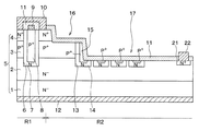
本発明の一実施形態を適用したSiC半導体装置として、JFETを備えたSiC半導体装置を例に挙げて説明する。図1は、本実施形態にかかるJFETを備えたSiC半導体装置を示した図であり、図1(a)が上面レイアウト図、(b)が(a)のA−A’断面図である。以下、この図に基づいて本実施形態にかかるJFETを備えたSiC半導体装置の構成について説明する。
まず、上記不純物濃度で構成されたN+型基板1を用意し、N+型基板1の表面に、N-型ドリフト層2、P+型層3およびN+型層4を順にエピタキシャル成長させることで半導体基板5を形成する。
フォトリソグラフィにより、トランジスタセル領域R1において、N+型層4およびP+型層3を貫通してN-型ドリフト層2に達するトレンチ6を形成すると同時に、外周耐圧構造領域R2においても、N+型層4およびP+型層3を貫通してN-型ドリフト層2に達するトレンチ13を形成する。本実施形態では、トレンチ6、13を同じ幅、同じ深さで形成している。
エピタキシャル成長法により、N-型SiCとP+型SiCを半導体基板5の表面全面にエピタキシャル成長させることにより、N-型層30およびP+型層31を形成し、これらによってトレンチ6、13内を埋め込む。
エッチバックやCMP(Chemical Mechanical Polishing)などによって半導体基板5の表面を平坦化することで、トレンチ6、13の内部にのみN-型層30およびP+型層31を残す。これにより、トレンチ6内にN-型チャネル層7およびP+型層8が形成されると共に、トレンチ13内にN-型層14およびP+型層15が形成される。
RIE(Reactive Ion Etching)等の異方性エッチングにより、トランジスタセル領域R1の外縁部において、N+型層4よりも深い位置までエッチングして凹部16を形成する。具体的には、凹部16の形成予定領域(外周耐圧構造領域R2)が開口するマスクを配置した後、異方性エッチングを行うことで凹部16を形成する。続いて、先ほど使用したマスクとは異なるマスクを用いて、再びRIE等の異方性エッチングにより、凹部16の底面における外縁部において、P+型層3よりも深い位置まで選択エッチングして凹第2部17を形成する。具体的には、凹部17の形成予定領域(セル領域の外縁部のうちP型リサーフ層15が配置される部分から外周側)が開口するマスクを配置した後、異方性エッチングを行うことで凹部17を形成する。このようにして、メサ構造が構成される。このとき、トレンチ13内に配置されたP+型層15によって凹部17の側面が構成されるようにしている。
イオン注入用のマスク32を配置したのち、P型領域18、19の形成予定領域に開口部を形成する。その後、基板表面に対する方線方向からP型不純物をイオン注入することで、P型領域18、19を形成する。このとき、図4(b)に示す工程において、トレンチ13内に配置されたP+型層15によって凹部17の側面が構成される様にしていることから、凹部16の底面に形成されたP型領域18と、トレンチ13内に配置されたP+型層15、および、凹部17の底面に形成されたP型領域19とが繋がり、これらによってP型リサーフ層20が構成される。
本発明の第2実施形態について説明する。本実施形態は、第1実施形態に対して外周耐圧構造領域R2の構造を変更したものであり、その他に関しては第1実施形態と同様であるため、異なる部分についてのみ説明する。
本発明の第3実施形態について説明する。本実施形態は、第2実施形態に対してガードリング構造の形状を変更したものであり、その他に関しては第2実施形態と同様であるため、異なる部分についてのみ説明する。
本発明の第4実施形態について説明する。本実施形態は、第2、第3実施形態に対してガードリング構造の形状を変更したものであり、その他に関しては第2、第3実施形態と同様であるため、異なる部分についてのみ説明する。
本発明の第5実施形態について説明する。本実施形態は、第1実施形態に対して、トランジスタセル領域R1に形成するトランジスタを変更したものであり、その他に関しては第1実施形態と同様であるため、異なる部分についてのみ説明する。
まず、上記不純物濃度で構成されたN+型基板1を用意し、N+型基板1の表面に、N-型ドリフト層2、P+型層3およびN+型層4を順にエピタキシャル成長させることで半導体基板5を形成する。
フォトリソグラフィにより、トランジスタセル領域R1において、N+型層4およびP+型層3を貫通してN-型ドリフト層2に達するトレンチ42を形成すると同時に、外周耐圧構造領域R2においても、N+型層4およびP+型層3を貫通してN-型ドリフト層2に達するトレンチ45を形成する。本実施形態では、トレンチ42、45を同じ幅、同じ深さで形成している。
エピタキシャル成長法により、P-型SiCもしくはN-型SiCとP+型SiCを半導体基板5の表面全面に順にエピタキシャル成長させることにより、低濃度層44、47およびP+型ディープ層43やP+型層46を形成し、これらによってトレンチ42、45内を埋め込む。
エッチバックやCMP(Chemical Mechanical Polishing)などによって半導体基板5の表面を平坦化する。これにより、トレンチ42、45の内部にのみ低濃度層44、47およびP+型ディープ層43やP+型層46が残された状態となる。
第1実施形態で説明した図4(b)と同様の工程を行うことで、凹部16および凹部17を形成する。これにより、メサ構造が構成される。このとき、トレンチ45内に配置されたP+型層46によって凹部17の側面が構成されるようにしている。
半導体基板5の表面全面にトレンチエッチング用マスク(図示せず)を配置した後、トレンチエッチングを行うことでトレンチ6を形成する。そして、熱酸化などによってゲート絶縁膜40を形成したのち、ドープトPoly−Si等を成膜することでトレンチ6内にゲート電極41を形成する。そして、エッチバックなどによってゲート電極41がトレンチ6内に残るように平坦化する。
本発明の第6実施形態について説明する。本実施形態は、第5実施形態に対して外周耐圧構造領域R2の構造を変更したものであり、その他に関しては第5実施形態と同様であるため、異なる部分についてのみ説明する。
本発明の第7実施形態について説明する。本実施形態は、第6実施形態に対してガードリング構造の形状を変更したものであり、その他に関しては第6実施形態と同様であるため、異なる部分についてのみ説明する。
本発明の第8実施形態について説明する。本実施形態は、第6、第7実施形態に対してガードリング構造の形状を変更したものであり、その他に関しては第6、第7実施形態と同様であるため、異なる部分についてのみ説明する。
上記実施形態では、電界緩和構造として、凹部16と凹部17の境界位置における凹部17の側面をP+型層15、46で構成し、これを用いてP型リサーフ層20やガードリング構造を構成することで外周耐圧構造を構成する場合について説明した。このような外周耐圧構造は、少なくとも凹部16と凹部17の境界位置における凹部17の側面をP+型層15、46で構成した電界緩和構造を含む構造であれば良く、電界緩和構造を用いたP型リサーフ層20やガードリング構造もしくはこれらの組み合わせなど、どのような構造の外周耐圧構造としても構わない。
2 N-型ドリフト層
3 P+型層
4 N+型層
5 半導体基板
6、13 トレンチ
7 N-型チャネル層
8、15 P+型層
9 第2ゲート電極
10 ソース電極
11 層間絶縁膜
12 ドレイン電極
14 N-型層
16 凹部(第2凹部)
17 凹部(第1凹部)
18、19 P型層
20 P型リサーフ層
40 ゲート絶縁膜
41 ゲート電極
42、45 トレンチ
43 P+型ディープ層
44、47 低濃度層
46 P+型層
Claims (22)
- 第1導電型基板(1)と、前記第1導電型基板(1)上に形成された第1導電型のドリフト層(2)と、前記ドリフト層(2)上に形成された第2導電型層(3)と、前記第2導電型層(3)上に形成された第1導電型層(4)とを有する炭化珪素からなる半導体基板(5)と、
前記半導体基板(5)のうちのトランジスタセル領域(R1)に形成されたトランジスタと、
前記トランジスタセル領域の外周を囲む外周耐圧構造領域(R2)に形成された外周耐圧構造とを有し、
前記外周耐圧構造領域(R2)に備えられた外周耐圧構造は、
前記トランジスタセル領域(R1)の外周を囲むように形成され、前記第1導電型層(4)と前記第2導電型層(3)よりも深く、前記ドリフト層(2)に達する第1凹部(17)と、
前記第1凹部(17)の内周側の側面の位置において、前記トランジスタ領域(R1)の外周を囲むように形成された第1トレンチ(13、45)と、
前記第1トレンチ(13、45)内に埋め込まれ、前記第1凹部(17)の側面を構成する第2導電型埋込層(15、46)を含む電界緩和構造と、を有した構成とされていることを特徴とする炭化珪素半導体装置。 - 前記第1導電型層(4)の厚みよりも深く、前記トランジスタセル領域(R1)の外周を囲むように形成された第2凹部(16)を有し、
前記第1凹部(17)は、前記第2凹部(16)よりも前記トランジスタセル領域(R1)の外周側に形成され、前記第2凹部(16)よりも深く形成されており、
前記第1トレンチ(13、45)は、前記第2凹部(16)と前記第1凹部(17)の境界位置に形成されていることを特徴とする請求項1に記載の炭化珪素半導体装置。 - 前記第2凹部(16)の底面のうち前記第1凹部(17)側と、前記第1凹部(17)の底面のうちの前記第2凹部(16)側には、前記第2導電型埋込層(15、46)に接続される第2導電型層(18、19)が形成され、これらの接続構造により構成される第2導電型リサーフ層(20)によって前記電界緩和構造が構成されていることを特徴とする請求項2に記載の炭化珪素半導体装置。
- 前記第1トレンチ(13、45)は、前記第2凹部(16)と前記第1凹部(17)との境界位置から更に外周側にも複数本形成され、前記第1トレンチ(13、45)それぞれに前記第2導電型埋込層(15、46)が備えられており、複数の前記第1トレンチ(13、45)内に備えられた前記第2導電型埋込層(15、46)により構成されるガードリング構造によって前記電界緩和構造が構成されていることを特徴とする請求項2に記載の炭化珪素半導体装置。
- 前記第2凹部(16)と前記第1凹部(17)との境界位置よりも内側にも形成され、前記第1トレンチ(13、45)それぞれに前記第2導電型埋込層(15、46)が備えられており、複数の前記第1トレンチ(13、45)内に備えられた前記第2導電型埋込層(15、46)により構成されるガードリング構造によって前記電界緩和構造が構成されていることを特徴とする請求項2または4に記載の炭化珪素半導体装置。
- 前記ガードリング構造を構成する前記第1トレンチ(13、45)は、前記トランジスタセル領域(R1)の外周方向に向かうに連れて幅が狭くされていることを特徴とする請求項4または5に記載の炭化珪素半導体装置。
- 前記トランジスタセル領域(R1)は、
前記第2導電型層(3)を第1ゲート領域とすると共に前記第1導電型層(4)をソース領域とし、
前記第1導電型層(4)および第2導電型層(3)を貫通して前記ドリフト層(2)まで達する第2トレンチ(6)と、
前記第2トレンチ(6)の内壁上にエピタキシャル成長によって形成された第1導電型のチャネル層(7)と、
前記チャネル層(7)の上に形成された第2導電型の第2ゲート領域(8)と、
前記第1導電型層(4)に電気的に接続されたソース電極(10)と、
前記第1導電型基板(1)に電気的に接続されたドレイン電極(12)とを有し、
前記第1ゲート領域(3)と前記第2ゲート領域(8)の少なくとも一方の電位を制御することにより、ソース−ドレイン間の電流を制御するJFETが形成されていることを特徴とする請求項1ないし6のいずれか1つに記載の炭化珪素半導体装置。 - 前記第1トレンチ(13)と前記第2トレンチ(6)が同じ深さとされ、前記第1トレンチ(13)には、第1導電型埋込層(14)を介して前記第2導電型埋込層(15)が形成されていることを特徴とする請求項7に記載の炭化珪素半導体装置。
- 前記トランジスタセル領域(R1)は、
前記第2導電型層(3)をベース領域とすると共に前記第1導電型層(4)をソース領域とし、
前記ソース領域と前記ドリフト層との間に位置する前記ベース領域の表面に形成されたゲート絶縁膜(40)と、
前記ゲート絶縁膜(40)の表面に形成されたゲート電極(41)と、
前記第1導電型層(4)に電気的に接続されたソース電極(10)と、
前記第1導電型基板(1)に電気的に接続されたドレイン電極(12)と、
前記第1導電型層(4)および第2導電型層(3)を貫通して前記ドリフト層(2)まで達する第2トレンチ(42)と、
前記第2トレンチ(42)内に埋め込まれた第2導電型のディープ層(43)とを有し、
前記ゲート電極(41)の電位を制御することにより、ソース−ドレイン間の電流を制御するMOSFETが形成されていることを特徴とする請求項1ないし6のいずれか1つに記載の炭化珪素半導体装置。 - 前記第1トレンチ(45)と前記第2トレンチ(42)が同じ深さとされていることを特徴とする請求項9に記載の炭化珪素半導体装置。
- 前記トランジスタセル領域(R1)には、
前記第1導電型層(4)および前記第2導電型層(3)を貫通して前記ドリフト層(2)まで達するトレンチ(6)が形成され、該トレンチ内(6)に前記ゲート絶縁膜(40)および前記ゲート電極(41)が形成されることで、前記MOSFETがトレンチゲート構造とされており、
該トレンチゲート構造における前記トレンチ(6)よりも前記第2トレンチ(42)の深さが深くされていることを特徴とする請求項9または10に記載の炭化珪素半導体装置。 - 第1導電型基板(1)と、前記第1導電型基板(1)上に形成された第1導電型のドリフト層(2)と、前記ドリフト層(2)上に形成された第2導電型層(3)と、前記第2導電型層(3)上に形成された第1導電型層(4)とを有する炭化珪素からなる半導体基板(5)と、
前記半導体基板(5)のうちのトランジスタセル領域(R1)に形成されたトランジスタと、
前記トランジスタセル領域の外周を囲む外周耐圧構造領域(R2)に形成された外周耐圧構造とを有してなる炭化珪素半導体装置の製造方法であって、
前記半導体基板(5)を用意する工程と、
前記外周耐圧構造領域(R2)に前記トランジスタ領域(R1)の外周を囲む第1トレンチ(13、45)を形成する工程と、
前記第1トレンチ(13、45)内に埋め込まれる第2導電型埋込層(15、46)を形成する工程と、
前記トランジスタセル領域(R1)の外周を囲むように、前記第1導電型層(4)と前記第2導電型層(3)よりも深く、前記ドリフト層(2)に達する第1凹部(17)を形成する工程とを含み、
前記第1凹部(17)を形成する工程では、前記第1トレンチ(13、45)が前記第1凹部(17)の内周側の側面となる場所に位置し、前記第1凹部(17)の側面が第2導電型埋込層(15、46)にて構成されるようにすることで、前記第2導電型埋込層(15、46)を含む電界緩和構造を構成することを特徴とする炭化珪素半導体装置の製造方法。 - 前記第1導電型層(4)の厚みよりも深く、前記トランジスタセル領域(R1)の外周を囲むように第2凹部(16)を形成する工程を含み、
前記第1凹部(17)を形成する工程では、前記第1トレンチ(13、45)が前記第2凹部(16)と前記第1凹部(17)との境界位置に位置し、前記第2凹部(16)と前記第1凹部(17)との境界位置における前記第1凹部(17)の側面が第2導電型埋込層(15、46)にて構成されるようにすることで、前記第2導電型埋込層(15、46)を含む電界緩和構造を構成することを特徴とする請求項12に記載の炭化珪素半導体装置の製造方法。 - 前記第2凹部(16)を形成する工程および前記第1凹部(17)を形成する工程の後に、基板表面にマスク(32)を形成し、該マスク(32)を用いて基板法線方向から第2導電型不純物をイオン注入することにより、前記第2凹部(16)の底面のうち前記第1凹部(17)側と、前記第1凹部(17)の底面のうちの前記第2凹部(16)側に、前記第2導電型埋込層(15、46)に接続される第2導電型層(18、19)を形成し、これらの接続構造により第2導電型リサーフ層(20)を構成することによって前記電界緩和構造を構成することを特徴とする請求項13に記載の炭化珪素半導体装置の製造方法。
- 前記第1トレンチ(13、45)を形成する工程では、前記第2凹部(16)と前記第1凹部(17)との境界位置から更に外周側にも前記第1トレンチ(13、45)を複数本形成し、
前記第2導電型埋込層(15、46)を形成する工程では、前記第1トレンチ(13、45)それぞれに前記第2導電型埋込層(15、46)が形成されるようにすることで、複数の前記第1トレンチ(13、45)内に備えられた前記第2導電型埋込層(15、46)により構成されるガードリング構造によって前記電界緩和構造が構成されるようにすることを特徴とする請求項12に記載の炭化珪素半導体装置の製造方法。 - 前記第1トレンチ(13、45)を形成する工程では、前記第2凹部(16)と前記第1凹部(17)との境界位置よりも内側にも前記第1トレンチ(13、45)を形成し、前記第1トレンチ(13、45)それぞれに前記第2導電型埋込層(15、46)が形成されるようにすることで、複数の前記第1トレンチ(13、45)内に備えられた前記第2導電型埋込層(15、46)により構成されるガードリング構造によって前記電界緩和構造が構成されるようにすることを特徴とする請求項12または15に記載の炭化珪素半導体装置の製造方法。
- 前記第1トレンチ(13、45)を形成する工程は、複数の前記トレンチ(13、45)が前記トランジスタセル領域(R1)の外周方向に向かうに連れて幅が狭くなるようにすることを特徴とする請求項15または16に記載の炭化珪素半導体装置の製造方法。
- 前記トランジスタセル領域(R1)において、
前記第1導電型層(4)および第2導電型層(3)を貫通して前記ドリフト層(2)まで達する第2トレンチ(6)を形成する工程と、
前記第2トレンチ(6)の内壁上にエピタキシャル成長によって第1導電型のチャネル層(7)を形成する工程と、
前記チャネル層(7)の上に第2導電型の第2ゲート領域(8)を形成する工程と、
前記第1導電型層(4)に電気的に接続されるソース電極(10)を形成する工程と、
前記第1導電型基板(1)に電気的に接続されるドレイン電極(12)を形成する工程とを有し、
前記第2導電型層(3)を第1ゲート領域とすると共に前記第1導電型層(4)をソース領域として、前記第1ゲート領域(3)と前記第2ゲート領域(8)の少なくとも一方の電位を制御することにより、ソース−ドレイン間の電流を制御するJFETを形成することを特徴とする請求項12ないし17のいずれか1つに記載の炭化珪素半導体装置の製造方法。 - 前記第1トレンチ(13)に第1導電型埋込層(14)を形成する工程を有し、
前記第2導電型埋込層(15)を形成する工程を前記第1トレンチ(13)に前記第1導電型埋込層(14)を形成した後に行い、
前記第1トレンチ(13)を形成する工程と前記第2トレンチ(6)を形成する工程とを同時に行い、
前記第1導電型埋込層(14)を形成する工程と前記チャネル層(7)を形成する工程とを同時に行い、
前記第2導電型埋込層(15)を形成する工程と前記第2ゲート領域(8)を形成する工程を同時に行うことを特徴とする請求項18に記載の炭化珪素半導体装置の製造方法。 - 前記トランジスタセル領域(R1)において、
前記第1導電型層(4)および第2導電型層(3)を貫通して前記ドリフト層(2)まで達する第2トレンチ(42)を形成する工程と、
前記第2トレンチ(42)内に埋め込まれる第2導電型のディープ層(43)を形成する工程と、
前記第2導電型層(3)をベース領域とすると共に前記第1導電型層(4)をソース領域として、前記ソース領域と前記ドリフト層との間に位置する前記ベース領域の表面にゲート絶縁膜(40)を形成する工程と、
前記ゲート絶縁膜(40)の表面にゲート電極(41)を形成する工程と、
前記第1導電型層(4)に電気的に接続されるソース電極(10)を形成する工程と、
前記第1導電型基板(1)に電気的に接続されるドレイン電極(12)を形成する工程とを有し、
前記ゲート電極(41)の電位を制御することにより、ソース−ドレイン間の電流を制御するMOSFETを形成することを特徴とする請求項12ないし17のいずれか1つに記載の炭化珪素半導体装置の製造方法。 - 前記第1トレンチ(45)を形成する工程と前記第2トレンチ(42)を形成する工程を同時に行い、
前記第2導電型埋込層(46)を形成する工程と前記ディープ層(43)を形成する工程を同時に行うことを特徴とする請求項20に記載の炭化珪素半導体装置の製造方法。 - 前記トランジスタセル領域(R1)において、
前記第1導電型層(4)および前記第2導電型層(3)を貫通して前記ドリフト層(2)まで達するトレンチ(6)を形成する工程を有し、該トレンチ内(6)に前記ゲート絶縁膜(40)および前記ゲート電極(41)を形成することで、前記MOSFETをトレンチゲート構造とし、該トレンチゲート構造における前記トレンチ(6)よりも前記第2トレンチ(42)の深さが深くなるようにすることを特徴とする請求項20または21に記載の炭化珪素半導体装置の製造方法。
Priority Applications (5)
| Application Number | Priority Date | Filing Date | Title |
|---|---|---|---|
| JP2011174774A JP5482745B2 (ja) | 2011-08-10 | 2011-08-10 | 炭化珪素半導体装置およびその製造方法 |
| PCT/JP2012/005040 WO2013021636A1 (ja) | 2011-08-10 | 2012-08-08 | 炭化珪素半導体装置およびその製造方法 |
| US14/129,998 US8901573B2 (en) | 2011-08-10 | 2012-08-08 | Silicon carbide semiconductor device and method of manufacturing the same |
| SE1450265A SE537601C2 (sv) | 2011-08-10 | 2012-08-08 | Kiselkarbidhalvledaranordning och förfarande för tillverkning av densamma |
| DE112012003282.9T DE112012003282B4 (de) | 2011-08-10 | 2012-08-08 | Siliciumcarbidhalbleitervorrichtung und Verfahren zum Herstellen derselben |
Applications Claiming Priority (1)
| Application Number | Priority Date | Filing Date | Title |
|---|---|---|---|
| JP2011174774A JP5482745B2 (ja) | 2011-08-10 | 2011-08-10 | 炭化珪素半導体装置およびその製造方法 |
Publications (2)
| Publication Number | Publication Date |
|---|---|
| JP2013038308A JP2013038308A (ja) | 2013-02-21 |
| JP5482745B2 true JP5482745B2 (ja) | 2014-05-07 |
Family
ID=47668171
Family Applications (1)
| Application Number | Title | Priority Date | Filing Date |
|---|---|---|---|
| JP2011174774A Expired - Fee Related JP5482745B2 (ja) | 2011-08-10 | 2011-08-10 | 炭化珪素半導体装置およびその製造方法 |
Country Status (5)
| Country | Link |
|---|---|
| US (1) | US8901573B2 (ja) |
| JP (1) | JP5482745B2 (ja) |
| DE (1) | DE112012003282B4 (ja) |
| SE (1) | SE537601C2 (ja) |
| WO (1) | WO2013021636A1 (ja) |
Families Citing this family (27)
| Publication number | Priority date | Publication date | Assignee | Title |
|---|---|---|---|---|
| JP6077380B2 (ja) * | 2013-04-24 | 2017-02-08 | トヨタ自動車株式会社 | 半導体装置 |
| JP2015032665A (ja) * | 2013-08-01 | 2015-02-16 | 住友電気工業株式会社 | ワイドバンドギャップ半導体装置 |
| US9425265B2 (en) * | 2013-08-16 | 2016-08-23 | Cree, Inc. | Edge termination technique for high voltage power devices having a negative feature for an improved edge termination structure |
| JP6231396B2 (ja) * | 2014-02-10 | 2017-11-15 | トヨタ自動車株式会社 | 半導体装置及び半導体装置の製造方法 |
| DK3133068T3 (da) * | 2014-04-14 | 2021-01-11 | Shanghai hengrui pharmaceutical co ltd | Amidderivater og farmaceutisk acceptable salte deraf, fremgangsmåde til fremstilling deraf og medicinske anvendelser deraf |
| JP6291988B2 (ja) | 2014-04-15 | 2018-03-14 | 住友電気工業株式会社 | 炭化珪素半導体装置 |
| JP6354525B2 (ja) * | 2014-11-06 | 2018-07-11 | 株式会社デンソー | 炭化珪素半導体装置の製造方法 |
| JP6613610B2 (ja) | 2015-05-14 | 2019-12-04 | 富士電機株式会社 | 半導体装置および半導体装置の製造方法 |
| JP6275353B2 (ja) | 2015-10-30 | 2018-02-07 | 三菱電機株式会社 | 炭化珪素半導体装置 |
| JP6705155B2 (ja) | 2015-11-13 | 2020-06-03 | 富士電機株式会社 | 半導体装置および半導体装置の製造方法 |
| JP6651894B2 (ja) * | 2016-02-23 | 2020-02-19 | 株式会社デンソー | 化合物半導体装置およびその製造方法 |
| JP6485382B2 (ja) * | 2016-02-23 | 2019-03-20 | 株式会社デンソー | 化合物半導体装置の製造方法および化合物半導体装置 |
| JP6470214B2 (ja) * | 2016-03-16 | 2019-02-13 | 株式会社東芝 | 半導体装置 |
| JP6696329B2 (ja) * | 2016-07-05 | 2020-05-20 | 株式会社デンソー | 炭化珪素半導体装置およびその製造方法 |
| JP6740759B2 (ja) * | 2016-07-05 | 2020-08-19 | 株式会社デンソー | 炭化珪素半導体装置およびその製造方法 |
| JP6658406B2 (ja) * | 2016-08-31 | 2020-03-04 | 株式会社デンソー | 炭化珪素半導体装置の製造方法 |
| JP6871562B2 (ja) * | 2016-11-16 | 2021-05-12 | 富士電機株式会社 | 炭化珪素半導体素子およびその製造方法 |
| US10861931B2 (en) | 2016-12-08 | 2020-12-08 | Cree, Inc. | Power semiconductor devices having gate trenches and buried edge terminations and related methods |
| JP6673232B2 (ja) * | 2017-01-17 | 2020-03-25 | 株式会社デンソー | 炭化珪素半導体装置 |
| US11817293B2 (en) * | 2020-01-10 | 2023-11-14 | The Research Foundation For The State University Of New York | Photoresist layers of semiconductor components including electric fields, system, and methods of forming same |
| JP7334678B2 (ja) * | 2020-06-04 | 2023-08-29 | 三菱電機株式会社 | 半導体装置 |
| CN112349771A (zh) * | 2020-09-30 | 2021-02-09 | 湖南大学 | 一种碳化硅器件埋层型终端结构及其制备方法 |
| KR102426997B1 (ko) * | 2020-12-30 | 2022-07-28 | 포항공과대학교 산학협력단 | 트리플 트렌치 구조를 구비하는 SiC 트랜지스터 및 그것의 제조 방법 |
| KR102426998B1 (ko) * | 2020-12-30 | 2022-07-28 | 포항공과대학교 산학협력단 | 트리플 트렌치 구조를 구비하는 Si 트랜지스터 및 그것의 제조 방법 |
| EP4510194A1 (en) * | 2022-04-14 | 2025-02-19 | Denso Corporation | Semiconductor device and method for producing same |
| CN115148826B (zh) * | 2022-09-06 | 2023-01-06 | 深圳平创半导体有限公司 | 一种深沟槽碳化硅jfet结构的制作方法 |
| CN117790537B (zh) * | 2023-12-28 | 2024-10-25 | 深圳平湖实验室 | 一种半导体器件、其制作方法及电子器件 |
Family Cites Families (10)
| Publication number | Priority date | Publication date | Assignee | Title |
|---|---|---|---|---|
| US6693308B2 (en) * | 2002-02-22 | 2004-02-17 | Semisouth Laboratories, Llc | Power SiC devices having raised guard rings |
| JP4051971B2 (ja) | 2002-03-15 | 2008-02-27 | 株式会社デンソー | 炭化珪素半導体装置およびその製造方法 |
| JP4179139B2 (ja) | 2003-11-14 | 2008-11-12 | 株式会社デンソー | 炭化珪素半導体装置およびその製造方法 |
| JP4857527B2 (ja) * | 2004-05-24 | 2012-01-18 | 株式会社デンソー | 炭化珪素半導体装置の製造方法 |
| DE102005023891B4 (de) | 2004-05-24 | 2009-08-27 | DENSO CORPORATION, Kariya-shi | Verfahren zum Herstellen einer Siliziumkarbid-Halbleitervorrichtung und Siliziumkarbid-Halbleitervorrichtung |
| EP2091083A3 (en) | 2008-02-13 | 2009-10-14 | Denso Corporation | Silicon carbide semiconductor device including a deep layer |
| JP2010147222A (ja) * | 2008-12-18 | 2010-07-01 | Denso Corp | 炭化珪素半導体装置およびその製造方法 |
| JP4683075B2 (ja) | 2008-06-10 | 2011-05-11 | 株式会社デンソー | 炭化珪素半導体装置およびその製造方法 |
| JP5326405B2 (ja) | 2008-07-30 | 2013-10-30 | 株式会社デンソー | ワイドバンドギャップ半導体装置 |
| JP5396953B2 (ja) * | 2009-03-19 | 2014-01-22 | 株式会社デンソー | 炭化珪素半導体装置およびその製造方法 |
-
2011
- 2011-08-10 JP JP2011174774A patent/JP5482745B2/ja not_active Expired - Fee Related
-
2012
- 2012-08-08 DE DE112012003282.9T patent/DE112012003282B4/de active Active
- 2012-08-08 SE SE1450265A patent/SE537601C2/sv unknown
- 2012-08-08 US US14/129,998 patent/US8901573B2/en active Active
- 2012-08-08 WO PCT/JP2012/005040 patent/WO2013021636A1/ja active Application Filing
Also Published As
| Publication number | Publication date |
|---|---|
| WO2013021636A1 (ja) | 2013-02-14 |
| SE537601C2 (sv) | 2015-07-14 |
| DE112012003282T5 (de) | 2014-04-30 |
| US8901573B2 (en) | 2014-12-02 |
| DE112012003282B4 (de) | 2025-02-06 |
| US20140145212A1 (en) | 2014-05-29 |
| JP2013038308A (ja) | 2013-02-21 |
| SE1450265A1 (sv) | 2014-03-07 |
Similar Documents
| Publication | Publication Date | Title |
|---|---|---|
| JP5482745B2 (ja) | 炭化珪素半導体装置およびその製造方法 | |
| JP5812029B2 (ja) | 炭化珪素半導体装置およびその製造方法 | |
| EP2755237B1 (en) | Trench MOS gate semiconductor device and method of fabricating the same | |
| US10134593B2 (en) | Semiconductor device and method for manufacturing same | |
| JP4798119B2 (ja) | 炭化珪素半導体装置およびその製造方法 | |
| JP5751213B2 (ja) | 炭化珪素半導体装置およびその製造方法 | |
| CN111344866B (zh) | 半导体装置及其制造方法 | |
| JP6048317B2 (ja) | 炭化珪素半導体装置 | |
| CN110050349B (zh) | 碳化硅半导体装置及其制造方法 | |
| JP4683075B2 (ja) | 炭化珪素半導体装置およびその製造方法 | |
| JP6179409B2 (ja) | 炭化珪素半導体装置の製造方法 | |
| JP5772842B2 (ja) | 炭化珪素半導体装置 | |
| JP5298565B2 (ja) | 半導体装置およびその製造方法 | |
| JP6485382B2 (ja) | 化合物半導体装置の製造方法および化合物半導体装置 | |
| JP5533677B2 (ja) | 炭化珪素半導体装置およびその製造方法 | |
| JP6914624B2 (ja) | 炭化珪素半導体装置およびその製造方法 | |
| JP2010147222A (ja) | 炭化珪素半導体装置およびその製造方法 | |
| JP6696328B2 (ja) | 炭化珪素半導体装置およびその製造方法 | |
| JP2016092257A (ja) | 炭化珪素半導体装置およびその製造方法 | |
| JP2012169386A (ja) | 炭化珪素半導体装置およびその製造方法 | |
| CN109417089B (zh) | 碳化硅半导体装置及其制造方法 | |
| JP2010034381A (ja) | ワイドバンドギャップ半導体装置 | |
| JP6870547B2 (ja) | 半導体装置およびその製造方法 | |
| JP7420485B2 (ja) | 炭化珪素半導体装置およびその製造方法 | |
| WO2017145548A1 (ja) | 化合物半導体装置およびその製造方法 |
Legal Events
| Date | Code | Title | Description |
|---|---|---|---|
| A621 | Written request for application examination |
Free format text: JAPANESE INTERMEDIATE CODE: A621 Effective date: 20121130 |
|
| TRDD | Decision of grant or rejection written | ||
| A01 | Written decision to grant a patent or to grant a registration (utility model) |
Free format text: JAPANESE INTERMEDIATE CODE: A01 Effective date: 20140121 |
|
| A61 | First payment of annual fees (during grant procedure) |
Free format text: JAPANESE INTERMEDIATE CODE: A61 Effective date: 20140203 |
|
| R151 | Written notification of patent or utility model registration |
Ref document number: 5482745 Country of ref document: JP Free format text: JAPANESE INTERMEDIATE CODE: R151 |
|
| R250 | Receipt of annual fees |
Free format text: JAPANESE INTERMEDIATE CODE: R250 |
|
| R250 | Receipt of annual fees |
Free format text: JAPANESE INTERMEDIATE CODE: R250 |
|
| R250 | Receipt of annual fees |
Free format text: JAPANESE INTERMEDIATE CODE: R250 |
|
| R250 | Receipt of annual fees |
Free format text: JAPANESE INTERMEDIATE CODE: R250 |
|
| R250 | Receipt of annual fees |
Free format text: JAPANESE INTERMEDIATE CODE: R250 |
|
| R250 | Receipt of annual fees |
Free format text: JAPANESE INTERMEDIATE CODE: R250 |
|
| LAPS | Cancellation because of no payment of annual fees |