CN101669026A - Utilize the method and apparatus of large-scale F ET array measurement analyte - Google Patents
Utilize the method and apparatus of large-scale F ET array measurement analyte Download PDFInfo
- Publication number
- CN101669026A CN101669026A CN200780051353A CN200780051353A CN101669026A CN 101669026 A CN101669026 A CN 101669026A CN 200780051353 A CN200780051353 A CN 200780051353A CN 200780051353 A CN200780051353 A CN 200780051353A CN 101669026 A CN101669026 A CN 101669026A
- Authority
- CN
- China
- Prior art keywords
- array
- chemical
- fets
- sensor
- fet
- Prior art date
- Legal status (The legal status is an assumption and is not a legal conclusion. Google has not performed a legal analysis and makes no representation as to the accuracy of the status listed.)
- Granted
Links
- 0 C*(C)CN** Chemical compound C*(C)CN** 0.000 description 1
- JKOUAAGYVJBILW-MSUUIHNZSA-N NCCCC(CN/C=C\NCc1ccc(CNCCNCCNC2)cc1)NCc1ccc2cc1 Chemical compound NCCCC(CN/C=C\NCc1ccc(CNCCNCCNC2)cc1)NCc1ccc2cc1 JKOUAAGYVJBILW-MSUUIHNZSA-N 0.000 description 1
Images


Classifications
-
- G—PHYSICS
- G01—MEASURING; TESTING
- G01N—INVESTIGATING OR ANALYSING MATERIALS BY DETERMINING THEIR CHEMICAL OR PHYSICAL PROPERTIES
- G01N27/00—Investigating or analysing materials by the use of electric, electrochemical, or magnetic means
- G01N27/26—Investigating or analysing materials by the use of electric, electrochemical, or magnetic means by investigating electrochemical variables; by using electrolysis or electrophoresis
- G01N27/403—Cells and electrode assemblies
- G01N27/414—Ion-sensitive or chemical field-effect transistors, i.e. ISFETS or CHEMFETS
- G01N27/4148—Integrated circuits therefor, e.g. fabricated by CMOS processing
-
- C—CHEMISTRY; METALLURGY
- C12—BIOCHEMISTRY; BEER; SPIRITS; WINE; VINEGAR; MICROBIOLOGY; ENZYMOLOGY; MUTATION OR GENETIC ENGINEERING
- C12Q—MEASURING OR TESTING PROCESSES INVOLVING ENZYMES, NUCLEIC ACIDS OR MICROORGANISMS; COMPOSITIONS OR TEST PAPERS THEREFOR; PROCESSES OF PREPARING SUCH COMPOSITIONS; CONDITION-RESPONSIVE CONTROL IN MICROBIOLOGICAL OR ENZYMOLOGICAL PROCESSES
- C12Q1/00—Measuring or testing processes involving enzymes, nucleic acids or microorganisms; Compositions therefor; Processes of preparing such compositions
- C12Q1/68—Measuring or testing processes involving enzymes, nucleic acids or microorganisms; Compositions therefor; Processes of preparing such compositions involving nucleic acids
- C12Q1/6813—Hybridisation assays
- C12Q1/6816—Hybridisation assays characterised by the detection means
- C12Q1/6818—Hybridisation assays characterised by the detection means involving interaction of two or more labels, e.g. resonant energy transfer
-
- C—CHEMISTRY; METALLURGY
- C12—BIOCHEMISTRY; BEER; SPIRITS; WINE; VINEGAR; MICROBIOLOGY; ENZYMOLOGY; MUTATION OR GENETIC ENGINEERING
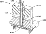
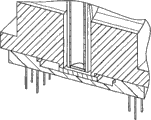
- C12Q—MEASURING OR TESTING PROCESSES INVOLVING ENZYMES, NUCLEIC ACIDS OR MICROORGANISMS; COMPOSITIONS OR TEST PAPERS THEREFOR; PROCESSES OF PREPARING SUCH COMPOSITIONS; CONDITION-RESPONSIVE CONTROL IN MICROBIOLOGICAL OR ENZYMOLOGICAL PROCESSES
- C12Q1/00—Measuring or testing processes involving enzymes, nucleic acids or microorganisms; Compositions therefor; Processes of preparing such compositions
- C12Q1/68—Measuring or testing processes involving enzymes, nucleic acids or microorganisms; Compositions therefor; Processes of preparing such compositions involving nucleic acids
- C12Q1/6869—Methods for sequencing
- C12Q1/6874—Methods for sequencing involving nucleic acid arrays, e.g. sequencing by hybridisation
-
- G—PHYSICS
- G01—MEASURING; TESTING
- G01N—INVESTIGATING OR ANALYSING MATERIALS BY DETERMINING THEIR CHEMICAL OR PHYSICAL PROPERTIES
- G01N27/00—Investigating or analysing materials by the use of electric, electrochemical, or magnetic means
- G01N27/26—Investigating or analysing materials by the use of electric, electrochemical, or magnetic means by investigating electrochemical variables; by using electrolysis or electrophoresis
- G01N27/403—Cells and electrode assemblies
- G01N27/414—Ion-sensitive or chemical field-effect transistors, i.e. ISFETS or CHEMFETS
- G01N27/4145—Ion-sensitive or chemical field-effect transistors, i.e. ISFETS or CHEMFETS specially adapted for biomolecules, e.g. gate electrode with immobilised receptors
-
- G—PHYSICS
- G01—MEASURING; TESTING
- G01N—INVESTIGATING OR ANALYSING MATERIALS BY DETERMINING THEIR CHEMICAL OR PHYSICAL PROPERTIES
- G01N33/00—Investigating or analysing materials by specific methods not covered by groups G01N1/00 - G01N31/00
- G01N33/48—Biological material, e.g. blood, urine; Haemocytometers
- G01N33/50—Chemical analysis of biological material, e.g. blood, urine; Testing involving biospecific ligand binding methods; Immunological testing
- G01N33/53—Immunoassay; Biospecific binding assay; Materials therefor
- G01N33/543—Immunoassay; Biospecific binding assay; Materials therefor with an insoluble carrier for immobilising immunochemicals
- G01N33/54366—Apparatus specially adapted for solid-phase testing
- G01N33/54373—Apparatus specially adapted for solid-phase testing involving physiochemical end-point determination, e.g. wave-guides, FETS, gratings
- G01N33/5438—Electrodes
-
- H—ELECTRICITY
- H10—SEMICONDUCTOR DEVICES; ELECTRIC SOLID-STATE DEVICES NOT OTHERWISE PROVIDED FOR
- H10D—INORGANIC ELECTRIC SEMICONDUCTOR DEVICES
- H10D30/00—Field-effect transistors [FET]
- H10D30/60—Insulated-gate field-effect transistors [IGFET]
-
- H—ELECTRICITY
- H10—SEMICONDUCTOR DEVICES; ELECTRIC SOLID-STATE DEVICES NOT OTHERWISE PROVIDED FOR
- H10D—INORGANIC ELECTRIC SEMICONDUCTOR DEVICES
- H10D84/00—Integrated devices formed in or on semiconductor substrates that comprise only semiconducting layers, e.g. on Si wafers or on GaAs-on-Si wafers
- H10D84/80—Integrated devices formed in or on semiconductor substrates that comprise only semiconducting layers, e.g. on Si wafers or on GaAs-on-Si wafers characterised by the integration of at least one component covered by groups H10D12/00 or H10D30/00, e.g. integration of IGFETs
- H10D84/82—Integrated devices formed in or on semiconductor substrates that comprise only semiconducting layers, e.g. on Si wafers or on GaAs-on-Si wafers characterised by the integration of at least one component covered by groups H10D12/00 or H10D30/00, e.g. integration of IGFETs of only field-effect components
- H10D84/83—Integrated devices formed in or on semiconductor substrates that comprise only semiconducting layers, e.g. on Si wafers or on GaAs-on-Si wafers characterised by the integration of at least one component covered by groups H10D12/00 or H10D30/00, e.g. integration of IGFETs of only field-effect components of only insulated-gate FETs [IGFET]
-
- H—ELECTRICITY
- H10—SEMICONDUCTOR DEVICES; ELECTRIC SOLID-STATE DEVICES NOT OTHERWISE PROVIDED FOR
- H10D—INORGANIC ELECTRIC SEMICONDUCTOR DEVICES
- H10D30/00—Field-effect transistors [FET]
- H10D30/60—Insulated-gate field-effect transistors [IGFET]
- H10D30/68—Floating-gate IGFETs
- H10D30/6891—Floating-gate IGFETs characterised by the shapes, relative sizes or dispositions of the floating gate electrode
-
- Y—GENERAL TAGGING OF NEW TECHNOLOGICAL DEVELOPMENTS; GENERAL TAGGING OF CROSS-SECTIONAL TECHNOLOGIES SPANNING OVER SEVERAL SECTIONS OF THE IPC; TECHNICAL SUBJECTS COVERED BY FORMER USPC CROSS-REFERENCE ART COLLECTIONS [XRACs] AND DIGESTS
- Y10—TECHNICAL SUBJECTS COVERED BY FORMER USPC
- Y10T—TECHNICAL SUBJECTS COVERED BY FORMER US CLASSIFICATION
- Y10T436/00—Chemistry: analytical and immunological testing
- Y10T436/22—Hydrogen, per se
Landscapes
- Life Sciences & Earth Sciences (AREA)
- Health & Medical Sciences (AREA)
- Chemical & Material Sciences (AREA)
- Engineering & Computer Science (AREA)
- Immunology (AREA)
- Molecular Biology (AREA)
- Proteomics, Peptides & Aminoacids (AREA)
- Organic Chemistry (AREA)
- Physics & Mathematics (AREA)
- General Health & Medical Sciences (AREA)
- Biochemistry (AREA)
- Analytical Chemistry (AREA)
- Wood Science & Technology (AREA)
- Zoology (AREA)
- Biotechnology (AREA)
- Microbiology (AREA)
- General Physics & Mathematics (AREA)
- Pathology (AREA)
- Urology & Nephrology (AREA)
- Hematology (AREA)
- Biomedical Technology (AREA)
- Microelectronics & Electronic Packaging (AREA)
- Bioinformatics & Cheminformatics (AREA)
- General Engineering & Computer Science (AREA)
- Genetics & Genomics (AREA)
- Chemical Kinetics & Catalysis (AREA)
- Electrochemistry (AREA)
- Biophysics (AREA)
- Cell Biology (AREA)
- Food Science & Technology (AREA)
- Medicinal Chemistry (AREA)
- Computer Hardware Design (AREA)
- Spectroscopy & Molecular Physics (AREA)
- Measuring Or Testing Involving Enzymes Or Micro-Organisms (AREA)
- Apparatus Associated With Microorganisms And Enzymes (AREA)
- Investigating Or Analyzing Materials By The Use Of Electric Means (AREA)
Abstract
Description
技术领域 technical field
本公开内容一般性涉及与利用电子传感器检测和测量一种或多种分析物有关的发明方法和装置。The present disclosure generally relates to inventive methods and devices related to the detection and measurement of one or more analytes using electronic sensors.
背景技术 Background technique
已经发现电子器件和元件在化学和生物学(一般称为“生命科学”)领域具有多种应用,特别适用于对化学反应和物质组成的各个方面的检测和测量。这些电子器件中的一种称作离子敏感场效应晶体管,其在有关文献中通常表示为ISFET(或pHFET)。ISFET通常主要由学术和研究团体研发用以简化溶液的氢离子浓度(通常称为“pH”)的测量。Electronic devices and components have found numerous applications in the fields of chemistry and biology (commonly referred to as "life sciences"), particularly for the detection and measurement of various aspects of chemical reactions and the composition of matter. One of these electronic devices is known as an ion-sensitive field-effect transistor, which is often denoted in the relevant literature as an ISFET (or pHFET). ISFETs have generally been developed primarily by the academic and research community to simplify the measurement of the hydrogen ion concentration (commonly referred to as "pH") of solutions.
更具体地,ISFET是一种阻抗变换器件,其以类似于MOSFET(金属氧化物半导体场效应晶体管)的方式工作,并特别设置为选择性测量溶液中的离子活性(例如溶液中的氢离子就是“分析物”)。“Thirty years ofISFETOLOGY:what happened in the past 30 years and what mayhappen in the next 30 years,”P.Bergveld,Sens.Actuators,88(2003),pp.1-20中给出了ISFET详细的工作原理,该出版物通过引用并入本文。More specifically, an ISFET is an impedance-transforming device that operates in a manner similar to a MOSFET (Metal Oxide Semiconductor Field Effect Transistor) and is specifically configured to selectively measure the activity of ions in solution (e.g. hydrogen ions in solution are "Analyte"). "Thirty years of ISFETOLOGY: what happened in the past 30 years and what may happen in the next 30 years," P. Bergveld, Sens. Actuators, 88 (2003), pp.1-20 gives a detailed working principle of ISFET, This publication is incorporated herein by reference.
图1示出利用常规CMOS(互补金属氧化物半导体)工艺制造的p型(p沟道)ISFET 50的截面图。基于p型硅衬底52来制造p型ISFET,其中形成构成晶体管“体”的n型阱54。构成ISFET的源极56和漏极58的高掺杂p型(p+)区域S和D形成在n型阱54中。还在n型阱中形成高掺杂n型(n+)区域B,以为n型阱提供导电体(或“块”)连接62。氧化层65设置在源极、漏极和体连接区域上方,形成穿过这些区域的开口从而为这些区域提供电连接(经由电导体)。例如,作为导体的金属接触66为漏极58提供电连接,而作为导体的金属接触68通过高导电的体连接62为源极56和n型阱54提供公用连接。多晶硅栅极64形成在源极56和漏极58之间的n型阱54的区域60上方位置处的氧化层上。因为氧化层65设置在多晶硅栅极64和晶体管体(即n型阱)之间,所以其通常称为“栅极氧化物”。FIG. 1 shows a cross-sectional view of a p-type (p-channel)
与MOSFET类似,ISFET 50是基于由多晶硅栅极64、栅极氧化物65和源极与漏极之间的n型阱54的区域60构成的MOS(金属-氧化物-半导体)电容所引起的电荷浓度调制来工作的。当跨接栅极和源极区域施加负电压时(VGS<0伏特),在栅极氧化物65和区域60的界面处通过耗尽该区域的电子而产生“p沟道”63。p沟道63在源极和漏极之间延伸,当栅极-源极电位VGS负到足以从源极将空穴吸引到沟道中时,电流传导通过p沟道。沟道63开始传导电流时的栅极-源极电位称作晶体管的阈值电压VTH(当VGS的绝对值大于阈值电压VTH时,导通晶体管)。源极之所以称为源极是因为其是流过沟道63的电荷载流子(对于p沟道来说是空穴)的来源;类似地,漏极是电荷载流子离开沟道63的位置。Similar to the MOSFET, the ISFET 50 is based on MOS (Metal-Oxide-Semiconductor) capacitance consisting of a
在图1的ISFET 50中,如金属接触68同时连接源极56和体连接62所示,通过体连接62将n型阱54(晶体管体)强制偏压到与源极56相同的电位(即VSB=0伏特)。这种连接避免了p+源极区域和n型阱的正向偏压,并因此有助于将电荷载流子限制到其中可形成沟道63的区域60的区域中。根据非线性关系,源极56和体/n型阱54之间的任何电位差(非零源-体电压VSB)都会影响ISFET的阈值电压VTH,且其通常称作“体效应”,这在许多应用中是不希望出现的。In ISFET 50 of FIG. 1, n-type well 54 (transistor body) is forced to be biased by
图1中还示出ISFET的多晶硅栅极64连接到设置在一个或多个置于栅极氧化物65上以构成“浮栅”结构70的附加氧化物层75中的多层金属层。之所以称为浮栅结构,是因为其与ISFET有关的其他导体电绝缘;即,其夹在栅极氧化物65和钝化层72之间。在ISFET 50中,钝化层72构成产生器件离子敏感性的离子敏感膜;即,接触钝化层72,特别是接触浮栅结构70上的敏感区域78中的钝化层72的“分析溶液”74(包含目标离子的溶液)中离子的存在改变了ISFET的电特性,从而调节流过源极56和漏极58之间p沟道63的电流。钝化层72可以包含有助于对特定离子敏感的各种不同材料中的任意一种;例如,包含氮化硅或氮氧化硅的钝化层通常提供对于分析物溶液74中的氢离子浓度(pH)的敏感性,而包含含有缬氨霉素的聚氯乙烯的钝化层提供对于分析物溶液中的钾离子浓度的敏感性(例如适用于钝化层并对诸如钠、银、铁、溴、碘、钙和硝酸根的其他离子敏感的材料是公知的)。Also shown in FIG. 1 is the
对于离子敏感性来说,由于化学反应(例如通常包括由敏感区域78附近的分析物溶液中的离子导致的氧化表面基团的分解),使得在钝化层72和分析物溶液74的固/液界面处出现的通常称作“表面电势”的电势差成为敏感区域78中离子浓度的函数。这种表面电势进而影响ISFET的阈值电压VTH;因此,ISFET的阈值电压VTH随着敏感区域78附近的分析物溶液74中的离子浓度的改变而变化。For ion sensitivity, due to chemical reactions (such as typically including the decomposition of oxidized surface groups caused by ions in the analyte solution near the sensitive region 78), the solid/ The potential difference, commonly referred to as the "surface potential," that occurs at the liquid interface becomes a function of the concentration of ions in the
图2示出图1所示的p沟道ISFET 50的等效电路。再次参考图1,分析物溶液74中的参比电极76(常规Ag/AgCl电极)测定分析物溶液本身的本体电位,并类似于常规MOSFET的栅极接线端,如图2所示。在ISFET的线性或不饱和工作区域中,漏电流ID由下式给出:FIG. 2 shows an equivalent circuit of p-
其中VDS是漏极和源极之间的电压,且β是跨导参数(单位为安培/伏特2),其由下式给出:where V DS is the voltage between drain and source, and β is the transconductance parameter in Amps/Volt 2 , which is given by:
其中μ表示载流子迁移率,Cox是每单位面积的栅极氧化物电容,比率W/L是沟道63的宽长比。如果参比电极76提供基准电压或接地电压(VG=0伏特),且漏电流ID和漏极-源极电压VDS保持恒定,则根据等式(1),ISFET的源极电压VS的变化直接跟踪阈值电压VTH的变化;这可以通过重排等式(1)观察到:where μ represents the carrier mobility, C ox is the gate oxide capacitance per unit area, and the ratio W/L is the width-to-length ratio of the
如上所述,因为ISFET的阈值电压VTH对离子浓度敏感,所以根据等式(3),源极电压VS提供了与ISFET的敏感区域78附近的分析物溶液74中的离子浓度直接相关的信号。在使用氮化硅或氮氧化硅的钝化层72用于检测pH灵敏度的典型常规ISFET中,已经观察到阈值电压灵敏度ΔVTH(即随着分析物溶液的pH变化而变化的阈值电压)为约30mV/pH至50mV/pH(298绝对温度下,理论最高灵敏度为59.2mV/pH)。As mentioned above, because the threshold voltage VTH of the ISFET is sensitive to ion concentration, according to equation (3), the source voltage VS provides a direct correlation with the ion concentration in the
先前的研究致力于制造基于常规CMOS工艺技术的用于pH测量的ISFET,其通常旨在实现1-14的pH的范围下的高信号线性度。具有约50mV/pH的典型阈值灵敏度,并考虑到上文的等式(3),这就要求源极电压VS具有约700mV的线性工作范围。如结合图1的以上讨论,ISFET(以及MOSFET)的阈值电压VTH受到源极和体(n型阱54)之间的任意电压VSB的影响。更具体地,阈值电压VTH是非零源-体电压VSB的非线性函数。因此,为了避免由于源极和体电位之间的差异而导致的折衷线性度(即缓和“体效应”),如图1所示,ISFET 50的源极56和体连接62通常通过金属接触68连接至公用电位。这种体-源连接还在图2所示的ISFET 50的等效电路中示出。Previous studies have been devoted to fabricating ISFETs for pH measurement based on conventional CMOS process technologies, which generally aim to achieve high signal linearity in the pH range of 1-14. With a typical threshold sensitivity of about 50mV/pH, and taking into account equation (3) above, this requires the source voltage VS to have a linear operating range of about 700mV. As discussed above in connection with FIG. 1 , the ISFET's (and MOSFET's) threshold voltage V TH is affected by any voltage V SB between the source and body (n-type well 54 ). More specifically, the threshold voltage VTH is a non-linear function of the non-zero source-body voltage VSB . Therefore, to avoid compromising linearity due to the difference between the source and body potentials (i.e. to moderate the "body effect"), as shown in FIG. Connect to common potential. This body-source connection is also shown in the equivalent circuit of
制造基于图1的ISFET设计的ISFET的二维阵列的先前工作已经制造出最大256的ISFET传感元件或阵列中的“像素”(即16乘16的像素阵列)。ISFET阵列制造的典型研究在出版物“A large transistor-based sensorarray chip for direct extracellular imaging”,M.J.Milgrew,M.O.Riehle,and D.R.S.Cumming,Sensors and Actuators,B:Chemical,111-112,(2005),pp.347-353,和“The development of scalable sensor arrays using standardCMOS technology”,M.J.Milgrew,P.A.Hammond,and D.R.S.Cumming,Sensors and Actuators,B:Chemical,103,(2004),pp.37-42中报道,这些出版物通过引用并入本文并在下文中简称为“Milgrew等人”。其他与实现ISFET阵列有关的研究工作在出版物“A very large integrated pH-ISFETsensor array chip compatible with standard CMOS processes”,T.C.W.Yeow,M.R.Haskard,D.E.Mulcahy,H.I.Seo and D.H.Kwon,Sensorsand Actuators B:Chemical,44,(1997),pp.434-440,以及“Fabrication of atwo-dimensional pH image sensor using a charge transfer technique”,Hizawa,T.,Sawada,K.,Takao,H.,Ishida,M.,Sensors and Actuators,B:Chemical 117(2),2006,pp.509-515中报道,这些出版物也通过引用并入本文。Previous work to fabricate two-dimensional arrays of ISFETs based on the ISFET design of FIG. 1 has fabricated a maximum of 256 ISFET sensing elements or "pixels" in the array (ie, a 16 by 16 pixel array). A typical study of ISFET array fabrication is in the publication "A large transistor-based sensorarray chip for direct extracellular imaging", M.J. Milgrew, M.O. Riehle, and D.R.S. Cumming, Sensors and Actuators, B: Chemical, 111-112, (2005), pp .347-353, and "The development of scalable sensor arrays using standard CMOS technology", M.J.Milgrew, P.A.Hammond, and D.R.S.Cumming, Sensors and Actuators, B: Chemical, 103, (2004), pp.37-42 reported, These publications are incorporated herein by reference and are hereinafter referred to simply as "Milgrew et al." Other research work related to the realization of ISFET arrays is in the publication "A very large integrated pH-ISFET sensor array chip compatible with standard CMOS processes", T.C.W.Yeow, M.R. Haskard, D.E.Mulcahy, H.I.Seo and D.H.Kwon, Sensors and Actuators B: Chemical, 44, (1997), pp.434-440, and "Fabrication of two-dimensional pH image sensor using a charge transfer technique", Hizawa, T., Sawada, K., Takao, H., Ishida, M., Sensors and Actuators, B: Chemical 117(2), 2006, pp.509-515, these publications are also incorporated herein by reference.
图3示出根据Milgrew等人的设计的二维ISFET阵列的一列85j。该列85j包括十六(16)个像素801至8016,并且如下文参考图7进一步讨论的,完整的二维阵列包括十六(16)个并排排列的这种列85j(j=1,2,3,....16)。如图3中所示,给出的列85j包括电流源ISOURCEj,其由该列中所有像素共用,且ISFET的偏置/读出电路82j(包括电流宿ISINKj)也由该列中所有像素共用。ISFET像素801至8016中的每一个都包括具有电连接源极和体的p沟道ISFET 50(如图1和2所示),加上对十六个行选择信号(RSEL1至RSEL16,以及它们的补码)之一响应的开关S1和S2。如下文参考图7所讨论的,行选择信号及其补码同时产生“启用”或选择列85j中的一个给定像素,且这种信号对以某种序列产生从而每次一个地顺序启用列中的不同像素。Figure 3 shows a column 85j of a two-dimensional ISFET array according to the design of Milgrew et al. The column 85 j includes sixteen (16)
如图3中所示,Milgrew等人的设计中的各个像素80的开关S2如常规n沟道MOSFET的情况一样执行,即当接收到相应的行选择信号时将电流源ISOURCEj连接至ISFET 50的源极。各个像素80的开关S1如传输门电路(transmission gate)即包括n沟道MOSFET和p沟道MOSFET的CMOS对的情况一样执行,即当接收到相应的行选择信号及其补码时将ISFET 50的源极连接至偏置/读出电路82j。图4中示出像素801的开关S11的一个实例,其中传输门的p沟道MOSFET表示为S11P,n沟道MOSFET表示为S11N。在Milgrew等人的设计中,各个像素的开关S1都使用传输门电路,因而对于启用的像素而言,在VDD至VSS的电源范围内的任何ISFET源极电压都可以施加到偏置/读出电路82j,并且按列输出为信号VSj。从上述内容中可以认识到Milgrew等人的ISFET传感器阵列设计中的各个像素80都包括四个晶体管,即p沟道ISFET、包括n沟道MOSFET和p沟道MOSFET的用作开关S1的CMOS对传输门电路、以及用作开关S2的n沟道MOSFET。As shown in Figure 3, the switch S2 of each
还如图3中所示,偏置/读出电路82j使用了开尔文电桥形式的源-漏极跟踪器构造,以保持恒定漏-源极电压VDSj并使源极电压VSj的测量与列85j中的启用像素的ISFET的恒定漏电流ISOURCEj隔离。为此,偏置/读出电路82j包括两个运算放大器A1和A2、电流宿ISINKj和电阻RSDj。运算放大器迫使由于电流ISINKj流过电阻产生的跨电阻RSDj发展的电压表现为跨越启用像素的ISFET的漏极和源极而成为恒定漏-源极电压VDSj。因此,再次参考等式(3),由于恒定的VDSj和恒定的ISOURCEj,所以启用像素的ISFET的源极电压VSj提供对应于ISFET阈值电压VTH的信号,并因此实现ISFET的敏感区域附近的pH的测量(参见图1)。通过传输门S1提供给源极电压VSj宽的动态范围,确保了可以测量从1-14的pH的全量程,且各个ISFET的源-体连接确保ISFET阈值电压在全pH量程范围下的足够线性度。As also shown in FIG. 3, bias/readout circuit 82j uses a source-drain tracker configuration in the form of a Kelvin bridge to maintain a constant drain-to-source voltage VDSj and to enable measurement of source voltage VSj Isolated from the constant drain current ISOURCEj of the ISFET of the enabled pixel in column 85j . To this end, the bias/readout circuit 82 j comprises two operational amplifiers A1 and A2, a current sink I SINKj and a resistor R SDj . The operational amplifier forces the voltage developed across resistance R SDj due to current I SINKj flowing through the resistor to appear as a constant drain-to-source voltage V DSj across the drain and source of the pixel-enabled ISFET. Thus, referring again to equation (3), due to constant V DSj and constant I SOURCEj , the source voltage V Sj of the ISFET of the enabled pixel provides a signal corresponding to the ISFET threshold voltage V TH and thus realizes the sensitive area of the ISFET nearby pH measurements (see Figure 1). The wide dynamic range provided to the source voltage V Sj by the transmission gate S1 ensures that the full range of pH from 1-14 can be measured, and the source-body connection of each ISFET ensures that the ISFET threshold voltage is sufficient in the full pH range. linearity.
在如图3中所示的Milgrew等人的列设计中,应当认识到对于发挥适当功能的列偏置/读出电路82j的开尔文电桥构造来说,必须在每个像素中使用如图1所示的p沟道ISFET 50;更具体地,基于开尔文电桥构造的替代实现方式不可能使用n沟道ISFET。再次参考图1,对于基于常规CMOS工艺的n沟道ISFET来说,无需n型阱54,并且将在p型硅衬底52(其将构成晶体管体)中直接形成用于漏极和源极的高掺杂n型区域。对于n沟道FET器件来说,晶体管体通常连接至电接地端。由于体效应的原因,所以Milgrew等人的设计中的ISFET的源极和体需要电连接在一起以缓和非线性特性,这将致使n沟道ISFET的源极也连接到电接地端(即VS=VB=0伏特),由此从启用的像素中排除了任何有用的输出信号。因此,图3中所示的Milgrew等人的列设计需要p沟道ISFET正常工作。In the column design of Milgrew et al. as shown in FIG. 3, it should be recognized that for the Kelvin bridge configuration of the column bias/readout circuit 82j to function properly, the 1 shows a p-
还可以认识到,在图3中所示的Milgrew等人的列设计中,需要在各个像素中实现开关S1和S2的两个n沟道MOSFET不能形成在图1中所示的n型阱54中,其中形成用于像素的p沟道ISFET;相反,n沟道MOSFET直接形成在p型硅衬底52中,超出了ISFET的n型阱54的范围。图5是与图1类似的图,示出与图3中所示的列85j的一个像素80对应的p型硅衬底52的一部分的宽截面图,其中在对应于开关S2的第一n沟道MOSFET和构成图4中所示的传输门S11的两个晶体管中一个的第二n沟道MOSFET S11N的旁边示出了包含ISFET 50的漏极58、源极56和体连接62的n型阱54。It can also be appreciated that in the column design of Milgrew et al. shown in FIG. 3, the two n-channel MOSFETs required to implement switches S1 and S2 in each pixel cannot be formed in the n-type well 54 shown in FIG. , where the p-channel ISFETs for the pixels are formed; in contrast, the n-channel MOSFETs are formed directly in the p-
而且,在Milgrew等人的设计中,在各个像素中实现传输门S1所需的p沟道MOSFET(例如参见附图4中的S11P)不能形成在其中形成有用于像素的p沟道ISFET 50的同一n型阱中。具体而言,因为p沟道ISFET的体和源极电连接在一起,所以在与p沟道ISFET 50相同的n-阱中实现p沟道MOSFET S11P将导致传输门不可预测的操作,或阻碍整体的操作。因此,Milgrew等人的设计中,需要两个隔离的n型阱来实现各个像素。图6是与图5类似的图,示出对应于一个像素80的p型硅衬底52的另一部分的截面,其中在形成有构成图4中所示的传输门S11的两个晶体管之一的p沟道MOSFET S11P的第二n型阱55旁边示出对应于ISFET 50的n型阱54。应当认识到图5和6中的图示并未按比例绘制,并且不能完全代表Milgrew等人的设计中的特定像素的实际布局;相反地,这些附图是概念性的,主要是为了说明Milgrew等人的设计中对于多个n-阱以及在n-阱之外制造隔离的n沟道MOSFET的需求。Also, in the design of Milgrew et al., the p-channel MOSFET required to implement transfer gate S1 in each pixel (see, for example, S1 1P in FIG. 4 ) cannot be formed in which p-
Milgrew等人的阵列设计利用0.35微米(μm)常规CMOS制造工艺来实现。在这种工艺中,各种设计规则规定了特征之间的最小间隔距离。例如,根据0.35μmCMOS设计规则,参考图6,相邻n-阱之间的距离“a”必须为至少三(3)微米。图6中还示出到n-阱54的左边和到n-阱55的右边的距离“a/2”,其表示将图6所示的像素80与左右分别相邻的其他列中的像素隔离所需的最小距离。而且,根据0.35μm CMOS设计规则,图6中所示的表示n型阱54的截面宽度的距离“b”和表示n型阱55的截面宽度的距离“c”都为约3μm至4μm(在n型阱中,n-阱边缘与源极和漏极之一间的公差为1.2μm,且源极和漏极本身的宽度为约0.7μm)。因此,图6中所示的表示截面图中的像素80的宽度的总距离“d”大致为约12μm至14μm。在一个实现方式中,Milgrew等人报道了一种基于图3中所示的列/像素设计的阵列,其包括几何方形的像素,每个像素都具有12.8μm×12.8μm的尺寸。The array design of Milgrew et al. is implemented using a 0.35 micron (μm) conventional CMOS fabrication process. In this process, various design rules dictate minimum separation distances between features. For example, according to the 0.35 μm CMOS design rules, referring to FIG. 6, the distance "a" between adjacent n-wells must be at least three (3) microns. Also shown in FIG. 6 is a distance “a/2” to the left of n-well 54 and to the right of n-well 55, which represents pixels in other columns adjacent to
总之,Milgrew等人的ISFET像素设计旨在确保在1-14的pH范围内的氢离子浓度的精确测量。为了确保测量的线性度,各个像素的ISFET的源极和体电连接在一起。为了确保pH测量的全量程,在各个像素中使用传输门S1来传送启用像素的源极电压。因此,Milgrew的阵列中的各个像素都需要四个晶体管(p沟道ISFET、p沟道MOSFET和两个n沟道MOSFET)以及两个隔离的n-阱(图6)。基于0.35微米常规CMOS制造工艺和相应的设计规则,这种阵列中的像素具有略大于10μm的最小尺寸,即为约12μm至14μm。In conclusion, the ISFET pixel design of Milgrew et al. aims to ensure accurate measurement of hydrogen ion concentration in the pH range of 1-14. In order to ensure the linearity of the measurement, the sources and bodies of the ISFETs of the individual pixels are electrically connected together. To ensure full-scale pH measurement, transfer gate S1 is used in each pixel to pass the source voltage to enable the pixel. Therefore, each pixel in Milgrew's array requires four transistors (p-channel ISFET, p-channel MOSFET, and two n-channel MOSFETs) and two isolated n-wells (FIG. 6). Based on a 0.35 micron conventional CMOS fabrication process and corresponding design rules, the pixels in such an array have a minimum dimension slightly larger than 10 μm, ie about 12 μm to 14 μm.
图7示出了根据Milgrew的设计的完整的二维像素阵列95以及附带的列译码器电路和测量读出电路。阵列95包括从851至8516的十六个列像素,各列都具有上文中结合图3所讨论的十六个像素(即16像素乘16像素的阵列)。行译码器92提供十六对互补码行选择信号,其中各对行选择信号都同时启用列851至8516各列中的一个像素,以基于ISFET的启用行的各个源极电压VS1至VS16,从阵列95提供一组列输出信号。行译码器92如常规四至十六位译码器(即,四位二进制输入ROW1-ROW4,以选择24输出中的一个)那样执行。用于阵列的启用行的列输出信号组VS1至VS16施加到开关逻辑电路96,其包括十六个传输门S1至S16(一个传输门对应一个输出信号)。如上所述,利用p沟道MOSFET和n沟道MOSFET来实现开关逻辑电路96的各个传输门电路,以确保各个输出信号VS1至VS16足够的动态范围。列译码器94与行译码器92类似,如常规四至十六位译码器那样执行,并通过四位二进制输入COL1-COL4来控制,以在任何给定时间处启用开关逻辑电路96的传输门S1至S16中的一个,从而从开关逻辑电路96提供一个输出信号VS。该输出信号VS施加到10位模-数转换器(ADC)98,以提供相应于阵列的给定像素的输出信号VS的数字表示D1-D10。Figure 7 shows a complete two-
如前所述,与前述相类似的独立ISFET和ISFET的阵列在涵盖化学和生物学的各种应用中已经用作传感装置。具体而言,ISFET已在涵盖诸如DNA的核酸的各种处理过程中用作pH传感器。下列出版物给出了在各种与生命科学有关的应用中使用ISFET的一些实例,这些出版物通过引用并入本文:Massimo Barbaro,Annalisa Bonfiglio,Luigi Raffo,AndreaAlessandrini,Paolo Facci and Imrich Barak,“Fully electronic DNAhybridization detection by a standard CMOS biochip,”Sensors andActuators B:Chemical,Volume 118,Issues 1-2,2006,pp.41-46;ToshinariSakurai and Yuzuru Husimi,“Real-time monitoring of DNA polymerasereactions by a micro ISFET pH sensor,”Anal.Chem.,64(17),1992,pp 1996-1997;S.Purushothaman,C.Toumazou,J.Georgiou,“Towards fast solidstate DNA sequencing,”Circuits and Systems,vol.4,2002,pp.IV-169 toIV-172;S.Purushothaman,C.Toumazou,C.P.Ou,“Protons and singlenucleotide polymorphism detection:A simple use for the Ion Sensitive FieldEffect Transistor,”Sensors and Actuators B:Chemical,Vol.114,no.2,2006,pp.964-968;A.L.Simonian,A.W.Flounders,J.R.Wild,“FET-BasedBiosensors for The Direct Detection of Organophosphate Neurotoxins,”Electroanalysis,Vol.16,No.22,2004,pp.1896-1906;C.Toumazou,S.Purushothaman,“Sensing Apparatus and Method,”United States PatentApplication 2004-0134798,published July 15,2004;and T.W.Koo,S.Chan,X.Su,Z.Jingwu,M.Yamakawa,V.M.Dubin,“Sensor Arrays and NucleicAcid Sequencing Applications,”United States Patent Application2006-0199193,published September 7,2006.As previously mentioned, individual ISFETs and arrays of ISFETs similar to those previously described have been used as sensing devices in a variety of applications covering chemistry and biology. Specifically, ISFETs have been used as pH sensors in various processes covering nucleic acids such as DNA. Some examples of the use of ISFETs in various life science-related applications are given in the following publications, which are incorporated herein by reference: Massimo Barbaro, Annalisa Bonfiglio, Luigi Raffo, Andrea Alessandrini, Paolo Facci and Imrich Barak, “Fully electronic DNAhybridization detection by a standard CMOS biochip," Sensors and Actuators B: Chemical,
通常,使用自动DNA定序器的快速且灵敏的核酸序列分析方法的发展已经显著推进了对于生物学的理解。术语“序列分析”是指无支链生物高分子的一级结构(或一级序列)的测定,其产生一种象征性的线性描述,称为“序列”,其简明地归纳了序列分子大量的原子级结构。“DNA序列测定”具体是指测定给定DNA碎片的核苷酸顺序的过程。现在,对于病毒、细菌、真菌、动物和植物的完整基因组的分析已经成为可能,但是由于序列测定的成本和容许能力的原因,这种分析通常受到限制。更具体而言,目前的常规序列测定方法在定序准确率、可以定序的独立模板的长度、定序的成本和序列测定速度方面受到限制。In general, the development of rapid and sensitive nucleic acid sequence analysis methods using automated DNA sequencers has significantly advanced the understanding of biology. The term "sequence analysis" refers to the determination of the primary structure (or primary sequence) of an unbranched biopolymer, which yields a symbolic linear description, called a "sequence", which concisely summarizes the sequence of a large number of molecules atomic-level structure. "DNA sequence determination" specifically refers to the process of determining the nucleotide sequence of a given DNA fragment. Analysis of complete genomes of viruses, bacteria, fungi, animals and plants is now possible, but often limited due to the cost and affordability of sequencing. More specifically, current conventional sequencing methods are limited in terms of sequencing accuracy, the length of independent templates that can be sequenced, the cost of sequencing, and the speed of sequencing.
尽管在样本制备和序列测定技术方面已经得到了改进,但是目前的常规序列测定策略,包括迄今可能涵盖ISFET的那些,已经提供了将容许能力提高到分析大量个体人类基因组所需的水平而需要的成本降低。有必要对大量个体基因组进行序列测定以了解疾病和衰老的遗传基础。此外,需要对大量的癌症进行序列测定以了解在癌症下的身体变化。近来的一些研究工作已经在制备用于序列测定的基因组的能力和同时对大量模板进行定序的能力方面取得了明显进步。但是,这些和其他研究工作仍然受到制备这些系统可检测的模板所需的相对大尺寸的反应体积的限制,以及对用以读出碱基的复杂的生化酶或荧光方法和特定核苷酸类似物的需要。Although improvements have been made in sample preparation and sequencing techniques, current routine sequencing strategies, including those likely to date encompassing ISFETs, have provided what is needed to increase permissive capacity to the levels required for the analysis of large numbers of individual human genomes. Reduce costs. Sequencing of large numbers of individual genomes is necessary to understand the genetic basis of disease and aging. Furthermore, a large number of cancers need to be sequenced to understand the body changes under cancer. Several recent research efforts have made significant advances in the ability to prepare genomes for sequencing and the ability to sequence large numbers of templates simultaneously. However, these and other research efforts are still limited by the relatively large size of the reaction volumes required to prepare the templates detectable by these systems, as well as the complex biochemical enzymatic or fluorescent methods used to read bases and specific nucleotide analogs. needs of things.
发明内容 Contents of the invention
申请人已经验证并认识到可特别地设置并应用大规模ISFET阵列以促进基于监测与DNA合成有关的化学过程中的变化的DNA序列测定技术。一般来说,申请人已经验证并认识到化学敏感FET的大规模阵列可用于检测和测量在许多化学和/或生物学过程(化学反应、细胞培养、神经活动、核酸序列测定等)中的各种分析物(例如氢离子、其他离子、非离子的分子或化合物、结合相互作用等等)的浓度/水平,其中基于这种分析物的测量可以获得有价值的信息。Applicants have demonstrated and realized that large-scale ISFET arrays can be specifically configured and applied to facilitate DNA sequencing techniques based on monitoring changes in the chemical processes associated with DNA synthesis. In general, applicants have verified and recognized that large-scale arrays of chemically sensitive FETs can be used to detect and measure various The concentration/level of an analyte (eg, hydrogen ions, other ions, non-ionic molecules or compounds, binding interactions, etc.), where valuable information can be obtained based on the measurement of such analytes.
因此,本公开内容的各个实施方案一般性涉及与用于测量一种或多种分析物的大规模FET阵列有关的发明方法和装置。在本文公开的各个实施方案中,FET阵列包括作为化学传感器的多个“化学FET”或化学敏感场效应晶体管。上述的ISFET是一种设置用于离子检测的特定类型的化学FET,且ISFET可用于本文公开的各个实施方案中。由本公开内容所披露的其他类型的化学FET包括ENFET,其设置用于特定酶的感测。但是应当认识到,本公开内容并不限于ISFET和ENFET,而是更一般地涉及设置用于某些类型的化学敏感性的任意FET。Accordingly, various embodiments of the present disclosure generally relate to inventive methods and devices related to large-scale FET arrays for measuring one or more analytes. In various embodiments disclosed herein, the FET array includes a plurality of "chemical FETs" or chemically sensitive field effect transistors as chemical sensors. The ISFET described above is a specific type of chemical FET configured for ion detection, and an ISFET may be used in various embodiments disclosed herein. Other types of chemical FETs disclosed by this disclosure include ENFETs configured for the sensing of specific enzymes. It should be appreciated, however, that the present disclosure is not limited to ISFETs and ENFETs, but more generally relates to any FET configured for certain types of chemical sensitivity.
根据其他实施方案,本公开内容一般性涉及与将合适的化学样本递送至上述大规模化学FET阵列以引起相应响应有关的发明方法和装置。化学样本可以包括小反应体积的(液体)分析物样本,以有助于对分析物进行高速、高密度的化学物(例如离子或其他组分)浓度或其他测量的检测。According to other embodiments, the present disclosure generally relates to inventive methods and devices related to the delivery of suitable chemical samples to the aforementioned large-scale chemical FET arrays to elicit corresponding responses. Chemical samples may include small reaction volumes of (liquid) analyte samples to facilitate high-speed, high-density detection of chemical (eg, ions or other components) concentrations or other measurements of analytes.
例如,一些实施方案涉及“非常大规模”二维化学FET传感器阵列(例如大于256k个传感器),其中构成这种阵列的传感器的一个或多个包含化学FET的元件或“像素”设置用以监测在阵列的像素附近发生的一个或多个独立的化学反应或事件。在一些示例性实施方式中,阵列可以连接到一个或多个在阵列的独立传感器或传感器组上形成一个或多个反应腔或“孔腔(well)”或“微孔腔(microwell)”的微流体结构和在测量过程之间将分析物样本递送到所述孔腔并将其从所述孔腔移除的装置。即使未使用微孔腔,传感器阵列也可以连接到用于在测量过程之间将一种或多种分析物递送到像素并移除该分析物的一个或多个微流体结构。因此,本公开内容的希望被保护的发明方面包括可以用于使试剂/分析物流动到孔腔或像素中以及使其从孔腔或像素中流出的各种微流体结构、孔腔阵列的制造方法、用于使阵列的像素与孔腔连接的方法和结构以及用于在装置用于DNA序列测定或相关分析时将负载DNA的微珠装载到孔腔中的方法和装置。For example, some embodiments relate to "very large-scale" two-dimensional chemical FET sensor arrays (e.g., greater than 256k sensors), wherein one or more chemical FET-containing elements or "pixels" of the sensors making up such an array are configured to monitor One or more independent chemical reactions or events that occur near the pixels of an array. In some exemplary embodiments, the array may be connected to one or more sensors forming one or more reaction chambers or "wells" or "microwells" on the array's individual sensors or groups of sensors. A microfluidic structure and means for delivering and removing an analyte sample to and from the well between measurements. Even if microcavities are not used, the sensor array can be connected to one or more microfluidic structures for delivery of one or more analytes to the pixels and removal of the analytes between measurements. Accordingly, the desired inventive aspects of the present disclosure include fabrication of various microfluidic structures, arrays of wells that can be used to flow reagents/analytes into and out of wells or pixels Methods, methods and structures for linking pixels of an array to wells and methods and devices for loading DNA-loaded beads into wells when the devices are used for DNA sequencing or related analysis.
还示出一种独特的参比电极及其与流动腔的连接。Also shown is a unique reference electrode and its connection to the flow chamber.
在各个实施方案中,特别关心的分析物是氢离子,并且根据本公开内容的大规模ISFET阵列特别设置为测量pH。在其他实施方案中,被监测的化学反应可以与DNA合成过程或其他化学和/或生物学过程有关,并且化学FET阵列可特别地设置为测量pH或一种或多种提供涉及感兴趣的特定化学过程的有关信息的其他分析物。在各个方面中,利用常规CMOS工艺技术制造化学FET阵列,并且化学FET阵列特别地设置为有助于快速获取来自整个阵列的数据(扫描所有像素以获得相应的像素输出信号)。In various embodiments, the analytes of particular interest are hydrogen ions, and the large-scale ISFET arrays according to the present disclosure are specifically configured to measure pH. In other embodiments, the chemical reaction being monitored may be related to the DNA synthesis process or other chemical and/or biological process, and the chemical FET array may be specifically configured to measure pH or one or more sensors related to a specific protein of interest. Other analytes for information about chemical processes. In various aspects, the chemical FET array is fabricated using conventional CMOS process technology and is specifically configured to facilitate fast acquisition of data from the entire array (scanning all pixels to obtain corresponding pixel output signals).
对于分析物检测和测量来说,应当认识到在下文详细讨论的各个实施方案中,根据本公开内容通过化学FET测量的一种或多种分析物可以包括提供关于所感兴趣的一个或多个化学过程(例如,多个核酸链的结合、抗体与抗原的结合等)的相关信息的任意多种化学物质。在某些方面中,除了仅检测分析物的存在之外,测量一种或多种分析物的水平或浓度的能力提供了与一个或多个化学过程有关的有价值的信息。在其他方面中,仅对所感兴趣的一种或多种分析物是否存在的检测可以提供有价值的信息。For analyte detection and measurement, it should be appreciated that in various embodiments discussed in detail below, one or more analytes measured by chemical FET according to the present disclosure may include providing information on one or more chemical FETs of interest. Any number of chemicals that provide information on processes (eg, binding of multiple nucleic acid strands, binding of antibodies to antigens, etc.). In certain aspects, the ability to measure the level or concentration of one or more analytes provides valuable information related to one or more chemical processes, in addition to merely detecting the presence of the analyte. In other aspects, the mere detection of the presence or absence of one or more analytes of interest can provide valuable information.
根据本公开内容的各个发明实施方案的化学FET阵列可以设置为对任意一种或多种不同分析物/化学物质具有敏感性。在一个实施方案中,阵列的一个或多个化学FET可以特别设置为对代表一种或多种结合事件(例如,与核酸序列测定过程有关的事件)的一种或多种分析物具有敏感性,并且在其他实施方案中,给定阵列的不同化学FET可以设置为对不同分析物具有敏感性。例如,在一个实施方案中,阵列的一个或多个传感器(像素)可以包括设置为对第一分析物化学敏感的第一类型化学FET,并且阵列的一个或多个其他传感器可以包括设置为对与第一分析物不同的第二分析物化学敏感的第二类型化学FET。在一个示例性实施方式中,第一分析物可以代表与核酸序列测定过程有关的第一结合事件,第二分析物可以代表与核酸序列测定过程有关的第二结合事件。当然,应当认识到可以在任意给定的阵列中使用多于两种的不同类型的化学FET以检测和/或测量不同类型的分析物/结合事件。一般来说,应当认识到,本文讨论的传感器阵列的任意实施方案中,给定的传感器阵列可以是“同质”的并且包括用以检测和/或测量相同类型的分析物(例如pH或其他离子浓度)的基本类似或相同类型的化学FET,或者传感器阵列可以是“异质”的并且包括用以检测和/或测量不同分析物的不同类型的化学FET。Chemical FET arrays according to various inventive embodiments of the present disclosure can be configured to be sensitive to any one or more different analytes/chemicals. In one embodiment, one or more chemical FETs of the array can be specifically configured to be sensitive to one or more analytes representing one or more binding events (e.g., events associated with a nucleic acid sequencing process) , and in other embodiments, different chemical FETs of a given array can be configured to be sensitive to different analytes. For example, in one embodiment, one or more sensors (pixels) of the array may include a first type chemical FET configured to be chemically sensitive to a first analyte, and one or more other sensors of the array may include a chemical FET configured to be chemically sensitive to a first analyte. A second type of chemical FET chemically sensitive to a second analyte different from the first analyte. In an exemplary embodiment, the first analyte may represent a first binding event associated with a nucleic acid sequencing process, and the second analyte may represent a second binding event associated with a nucleic acid sequencing process. Of course, it should be appreciated that more than two different types of chemical FETs may be used in any given array to detect and/or measure different types of analytes/binding events. In general, it should be recognized that in any of the embodiments of sensor arrays discussed herein, a given sensor array may be "homogeneous" and include sensors for detecting and/or measuring the same type of analyte (e.g., pH or other ion concentration), or the sensor array may be "heterogeneous" and include different types of chemical FETs to detect and/or measure different analytes.
在另外的方面中,申请人特别对与图1-7有关的上述Milgrew等人的ISFET阵列设计以及其他常规ISFET阵列设计加以改进,以便显著降低像素尺寸,并因此增加对于给定半导体芯片尺寸的化学FET阵列的像素数量(即增加像素密度)。在各个实施方案中,在实现像素密度增加的同时,增加对应于涉及所监测的化学过程的相应测量的输出信号的信噪比(SNR)以及增加从阵列读取这种输出信号的速度。特别地,申请人已经验证并认识到通过放松对化学FET线性度的要求并将注意力集中在进一步限制测量输出信号范围(例如对应于从约7至9而不是从1至14的pH范围的输出信号),可以显著降低独立像素的复杂性和尺寸,由此有助于实现非常大规模密集的化学FET阵列。申请人还验证并认识到针对化学FET阵列中的像素选择的替代性简单方法(可替代如图7中所示的Milgrew等人的设计中所使用的复杂性与阵列规模成比例的行和列译码器的方法)有助于快速获取来自非常大和密集的阵列中的数据。In a further aspect, applicants have modified the Milgrew et al. ISFET array design described above in relation to FIGS. 1-7, as well as other conventional ISFET array designs, to significantly reduce pixel size and thus increase the Pixel count (i.e. increasing pixel density) for chemical FET arrays. In various embodiments, an increase in pixel density is achieved while increasing the signal-to-noise ratio (SNR) of an output signal corresponding to a corresponding measurement involving the chemical process being monitored and increasing the speed at which such output signal is read from the array. In particular, applicants have verified and realized that by relaxing the requirements on chemical FET linearity and focusing on further limiting the measurement output signal range (e.g. corresponding to a pH range from about 7 to 9 rather than from 1 to 14 output signal), which can significantly reduce the complexity and size of individual pixels, thereby facilitating the realization of very large-scale dense chemical FET arrays. Applicants have also validated and recognized an alternative simple approach to pixel selection in chemical FET arrays (alternative to the row and column complexity used in Milgrew et al's design as shown in Figure 7 Decoder approach) helps to quickly acquire data from very large and dense arrays.
对于化学FET阵列的制造来说,申请人进一步验证并认识到常规CMOS制造工艺中使用的各种技术以及各种后制造工艺步骤(晶片传送、清洗、切割、封装等)会在某些情况下对所得的化学FET阵列的性能产生不利影响。例如,再次参考图1,一个潜在的问题涉及到俘获电荷,其可能在与浮栅结构70有关的金属的蚀刻期间在栅极氧化物65中产生,以及这种俘获电荷会怎样影响化学FET的阈值电压VTH。另一个潜在的问题涉及到由在铝基金属CMOS制造中所通常使用的低温材料沉积工艺制得的化学FET钝化层(例如参见图1中的ISFET钝化层72)的密度/孔隙度。虽然这种低温工艺通常为常规CMOS器件提供适宜的钝化层,但是它们可能导致可观的低密度和多孔的钝化层,其可能对接触分析物溶液的化学FET构成潜在的问题;特别是随着时间的流逝,低密度多孔钝化层会吸附溶液中的分析物或其他物质并被其饱和,这进而可能导致不希望的化学FET的阈值电压VTH的时变漂移。这种现象进而又阻碍所感兴趣的一种或多种特定分析物的精确测量。鉴于前述情况,本文公开的其它发明实施方案涉及用于减少对化学FET性能具有潜在不利影响的方法和装置,这可从化学FET阵列的制造和后制造工艺/处理的不同方面获得。For the fabrication of chemical FET arrays, Applicant further validates and recognizes that various techniques used in conventional CMOS fabrication processes as well as various post-manufacturing process steps (wafer handling, cleaning, dicing, packaging, etc.) Detrimentally affects the performance of the resulting chemical FET array. For example, referring again to FIG. 1, one potential problem involves trapped charge that may be generated in
因此,本发明的一个实施方案涉及一种装置,其包括CMOS制造的传感器阵列,每个传感器包括一个化学敏感场效应晶体管(化学FET)并且在阵列表面上占据10×10微米或更小的面积。Accordingly, one embodiment of the present invention is directed to a device comprising an array of CMOS fabricated sensors, each sensor comprising a chemically sensitive field effect transistor (chemical FET) and occupying an area of 10 x 10 microns or less on the surface of the array .
另一实施方案涉及一种传感器阵列,其包括二维电子传感器阵列,该阵列包括至少512行和至少512列的电子传感器,每个传感器包括一个化学敏感场效应晶体管(化学FET),其设置为提供表示二维阵列的表面附近的分析物的存在和/或浓度的至少一个输出信号。Another embodiment relates to a sensor array comprising a two-dimensional electronic sensor array comprising at least 512 rows and at least 512 columns of electronic sensors, each sensor comprising a chemically sensitive field effect transistor (chemical FET) arranged as At least one output signal indicative of the presence and/or concentration of an analyte near the surface of the two-dimensional array is provided.
另一实施方案涉及一种装置,其包括CMOS制造的传感器阵列,每个传感器包括一个化学敏感场效应晶体管(化学FET)。CMOS制造的传感器阵列包括多于256个传感器,并且来自阵列的所有化学FET的化学FET输出信号的集合构成数据帧。该装置还包括控制电路,其连接到阵列并设置为产生至少一个阵列输出信号从而以至少1帧每秒的帧速提供来自阵列的多个数据帧。在一个方面中,帧速可以是至少10帧每秒。在另一方面中,帧速可以是至少20帧每秒。在其他方面中,帧速可以是至少30、40、50、70或直至100帧每秒。Another embodiment relates to a device comprising an array of CMOS fabricated sensors, each sensor comprising a chemically sensitive field effect transistor (chemical FET). The CMOS fabricated sensor array includes more than 256 sensors, and the collection of chemical FET output signals from all chemical FETs of the array constitutes a data frame. The apparatus also includes control circuitry coupled to the array and configured to generate at least one array output signal to provide a plurality of frames of data from the array at a frame rate of at least 1 frame per second. In one aspect, the frame rate can be at least 10 frames per second. In another aspect, the frame rate may be at least 20 frames per second. In other aspects, the frame rate can be at least 30, 40, 50, 70, or up to 100 frames per second.
另一实施方案涉及一种装置,其包括CMOS制造的传感器阵列,每个传感器包括化学敏感场效应晶体管(化学FET)。该化学FET包括浮栅结构以及具有第一半导体类型并制造在具有第二半导体类型的区域中的源极和漏极,其中不存在将具有第二半导体类型的区域电连接至源极或漏极中任意其一的电导体。Another embodiment relates to a device comprising an array of CMOS fabricated sensors, each sensor comprising a chemically sensitive field effect transistor (chemical FET). The chemical FET includes a floating gate structure and a source and a drain having a first semiconductor type fabricated in a region of a second semiconductor type, wherein there is no electrical connection of the region of the second semiconductor type to the source or drain Any one of the electrical conductors.
另一实施方案涉及一种装置,其包括电子传感器阵列,每个传感器由包括一个化学敏感场效应晶体管(化学FET)的三个场效应晶体管(FET)构成。Another embodiment relates to a device comprising an array of electronic sensors, each sensor consisting of three field effect transistors (FETs) including one chemically sensitive field effect transistor (Chemical FET).
另一实施方案涉及一种装置,其包括电子传感器阵列,每个传感器包括三个或更少的场效应晶体管(FET),其中所述三个或更少的场效应晶体管(FET)包括一个化学敏感场效应晶体管(化学FET)、Another embodiment is directed to a device comprising an array of electronic sensors, each sensor comprising three or fewer field effect transistors (FETs), wherein the three or fewer field effect transistors (FETs) comprise a chemical Sensitive Field Effect Transistors (Chemical FETs),
另一实施方案涉及一种装置,其包括电子传感器阵列,每个传感器包括多个场效应晶体管(FET),所述多个场效应晶体管(FET)包括一个化学敏感场效应晶体管(化学FET),并且多个电导体电连接到所述多个FET,其中所述多个FET设置为使得所述多个电导体包括横穿被阵列的各个传感器所占据的区域并互连多个传感器的不多于四个电导体。Another embodiment is directed to an apparatus comprising an array of electronic sensors, each sensor comprising a plurality of field effect transistors (FETs), the plurality of field effect transistors (FETs) including a chemically sensitive field effect transistor (chemical FET), and a plurality of electrical conductors electrically connected to the plurality of FETs, wherein the plurality of FETs are arranged such that the plurality of electrical conductors comprise a plurality of FETs that traverse the area occupied by the individual sensors of the array and interconnect the plurality of sensors on four electrical conductors.
另一实施方案涉及一种装置,其包括CMOS制造的传感器阵列,每个传感器包括多个场效应晶体管(FET),所述多个场效应晶体管(FET)包括一个化学敏感场效应晶体管(化学FET),其中每个传感器中所有的FET都具有相同的沟道类型并且在阵列衬底的单一半导体区域中实现。Another embodiment relates to a device comprising an array of CMOS fabricated sensors, each sensor comprising a plurality of field effect transistors (FETs) including a chemically sensitive field effect transistor (Chemical FET ), where all FETs in each sensor have the same channel type and are implemented in a single semiconductor region of the array substrate.
另一实施方案涉及一种传感器阵列,其包括排列成多个行和多个列的多个电子传感器。每个传感器包括一个化学敏感场效应晶体管(化学FET),其设置为提供表示阵列的表面附近的分析物的存在和/或浓度的至少一个输出信号。对多个列中的每一列来说,阵列还包括列电路,其设置为对该列中相应的化学FET提供恒定的漏电流和恒定的漏-源极电压,列电路包括两个运算放大器和与相应的化学FET排列成开尔文电桥构造的二极管连接FET以提供恒定的漏-源极电压。Another embodiment relates to a sensor array comprising a plurality of electronic sensors arranged in a plurality of rows and a plurality of columns. Each sensor includes a chemically sensitive field effect transistor (chemical FET) arranged to provide at least one output signal indicative of the presence and/or concentration of an analyte near the surface of the array. For each of the plurality of columns, the array also includes column circuitry arranged to provide a constant drain current and a constant drain-to-source voltage to corresponding chemical FETs in the column, the column circuitry including two operational amplifiers and Diode connected FETs are arranged in a Kelvin bridge configuration with corresponding chemical FETs to provide a constant drain-source voltage.
另一实施方案涉及一种传感器阵列,其包括排列成多个行和多个列的多个电子传感器。每个传感器包括一个化学敏感场效应晶体管(化学FET),其设置为提供表示阵列的表面附近的分析物中离子浓度的至少一个输出信号。该阵列还包括用以开启多个行中相应的行的至少一个行选择移位寄存器,以及用以从多个列中相应的列获取化学FET输出信号的至少一个列选择移位寄存器。Another embodiment relates to a sensor array comprising a plurality of electronic sensors arranged in a plurality of rows and a plurality of columns. Each sensor includes a chemically sensitive field effect transistor (chemical FET) arranged to provide at least one output signal indicative of the concentration of ions in the analyte near the surface of the array. The array also includes at least one row select shift register to turn on a corresponding row of the plurality of rows, and at least one column select shift register to obtain a chemical FET output signal from a corresponding column of the plurality of columns.
另一实施方案涉及一种装置,其包括CMOS制造的传感器阵列,每个传感器包括化学敏感场效应晶体管(化学FET)。该化学FET包括浮栅结构以及具有第一半导体类型并制造在具有第二半导体类型的区域中的源极和漏极,其中不存在将具有第二半导体类型的区域电连接至源极或漏极的电导体。该阵列包括至少512行和至少512列的CMOS制造的传感器的二维阵列。每个传感器由包括化学FET的三个场效应晶体管(FET)构成,并且每个传感器包括电连接到所述三个FET的多个电导体。所述三个FET设置为使得所述多个电导体包括横穿过被阵列的各个传感器所占据的区域并互连多个传感器的不多于四个电导体。各个传感器中所有的FET都具有相同的沟道类型并且在阵列衬底的单一半导体区域中实现。来自阵列中所有化学FET的化学FET输出信号的集合构成数据帧。该装置还包括连接到阵列的控制电路并且设置为产生至少一个阵列输出信号,从而以至少20帧每秒的帧速提供来自阵列的多个数据帧。Another embodiment relates to a device comprising an array of CMOS fabricated sensors, each sensor comprising a chemically sensitive field effect transistor (chemical FET). The chemical FET includes a floating gate structure and a source and a drain having a first semiconductor type fabricated in a region of a second semiconductor type, wherein there is no electrical connection of the region of the second semiconductor type to the source or drain electrical conductors. The array includes a two-dimensional array of at least 512 rows and at least 512 columns of CMOS fabricated sensors. Each sensor is composed of three field effect transistors (FETs) including chemical FETs, and each sensor includes a plurality of electrical conductors electrically connected to the three FETs. The three FETs are arranged such that the plurality of electrical conductors includes no more than four electrical conductors traversing an area occupied by individual sensors of the array and interconnecting the plurality of sensors. All FETs in each sensor have the same channel type and are implemented in a single semiconductor region of the array substrate. The collection of chemical FET output signals from all chemical FETs in the array constitutes the data frame. The apparatus also includes control circuitry coupled to the array and configured to generate at least one array output signal to provide a plurality of frames of data from the array at a frame rate of at least 20 frames per second.
另一实施方案涉及一种加工CMOS制造的传感器的阵列的方法,每个传感器包括一个化学敏感场效应晶体管(化学FET)。该方法包括:A)切割包括阵列的半导体晶片以形成包括阵列的至少一个切割部分;以及B)对所述至少一个切割部分实施合成气体(forming gas)退火。Another embodiment relates to a method of processing an array of CMOS fabricated sensors, each sensor comprising a chemically sensitive field effect transistor (chemical FET). The method includes: A) dicing a semiconductor wafer including the array to form at least one diced portion including the array; and B) subjecting the at least one diced portion to a forming gas anneal.
另一实施方案涉及一种加工CMOS制造的传感器的阵列的方法。每个传感器包括一个化学敏感场效应晶体管(化学FET),其具有通过等离子体增强化学气相沉积(PECVD)而沉积的氮化硅和/或氮氧化硅的化学敏感钝化层。该方法包括:A)在化学敏感钝化层上沉积至少一种附加钝化材料以降低钝化层的孔隙度和/或增加钝化层的密度。Another embodiment relates to a method of processing an array of CMOS fabricated sensors. Each sensor comprises a chemically sensitive field effect transistor (chemical FET) with a chemically sensitive passivation layer of silicon nitride and/or silicon oxynitride deposited by plasma enhanced chemical vapor deposition (PECVD). The method includes: A) depositing at least one additional passivation material on the chemically sensitive passivation layer to reduce the porosity of the passivation layer and/or increase the density of the passivation layer.
另一方面,本发明提供一种用于核酸序列测定的方法,其包括将多个模板核酸设置在多个反应腔中,其中所述多个反应腔接触化学敏感场效应晶体管(化学FET)阵列,该阵列包括每个反应腔至少一个的化学FET,其中每个模板核酸与序列测定引物杂交并结合至聚合酶,通过在序列测定引物的3’端处顺序加入一种或多种公知的核苷三磷酸来合成新的核酸链,通过所述至少一个化学FET的电流变化来检测一种或多种公知的核苷三磷酸的加入。In another aspect, the present invention provides a method for nucleic acid sequence determination, comprising arranging a plurality of template nucleic acids in a plurality of reaction chambers, wherein the plurality of reaction chambers are in contact with an array of chemically sensitive field effect transistors (chemical FETs) , the array includes at least one chemical FET per reaction chamber, wherein each template nucleic acid hybridizes to a sequencing primer and binds to a polymerase by sequentially adding one or more well-known nuclei at the 3' end of the sequencing primer. glycoside triphosphates are used to synthesize new nucleic acid strands, and the addition of one or more known nucleoside triphosphates is detected by a change in current of the at least one chemical FET.
另一方面,本发明提供一种用于核酸序列测定的方法,其包括将多个模板核酸设置在多个反应腔中,其中所述多个反应腔接触化学敏感场效应晶体管(化学FET)阵列,该阵列包括每个反应腔至少一个的化学FET,其中每个模板核酸与序列测定引物杂交并结合至聚合酶,通过在序列测定引物的3’端处顺序加入一种或多种公知的核苷三磷酸来合成新的核酸链,通过至少一个化学FET的电流变化来检测一种或多种公知的核苷三磷酸的加入,其中该化学FET阵列是前述阵列中的任意一种。In another aspect, the present invention provides a method for nucleic acid sequence determination, comprising arranging a plurality of template nucleic acids in a plurality of reaction chambers, wherein the plurality of reaction chambers are in contact with an array of chemically sensitive field effect transistors (chemical FETs) , the array includes at least one chemical FET per reaction chamber, wherein each template nucleic acid hybridizes to a sequencing primer and binds to a polymerase by sequentially adding one or more well-known nuclei at the 3' end of the sequencing primer. The addition of one or more known nucleoside triphosphates is detected by a change in the current of at least one chemical FET, wherein the chemical FET array is any one of the aforementioned arrays.
另一方面,本发明提供一种用于核酸序列测定的方法,其包括将多个模板核酸设置在多个反应腔中,其中所述多个反应腔接触化学敏感场效应晶体管(化学FET)阵列,该阵列包括每个反应腔至少一个的化学FET,其中每个模板核酸与序列测定引物杂交并结合至聚合酶,通过在序列测定引物的3’端处顺序加入一种或多种公知的核苷三磷酸来合成新的核酸链,通过序列测定反应副产物的产生来检测一种或多种公知的核苷三磷酸的加入,其中(a)化学FET阵列包括多于256个传感器,或(b)相邻反应腔之间的中心距离(或“间距”)是1~10μm。In another aspect, the present invention provides a method for nucleic acid sequence determination, comprising arranging a plurality of template nucleic acids in a plurality of reaction chambers, wherein the plurality of reaction chambers are in contact with an array of chemically sensitive field effect transistors (chemical FETs) , the array includes at least one chemical FET per reaction chamber, wherein each template nucleic acid hybridizes to a sequencing primer and binds to a polymerase by sequentially adding one or more well-known nuclei at the 3' end of the sequencing primer. glycoside triphosphates to synthesize new nucleic acid strands, the addition of one or more known nucleoside triphosphates is detected by the generation of by-products of the sequencing reaction, wherein (a) the chemical FET array includes more than 256 sensors, or ( b) The center-to-center distance (or "pitch") between adjacent reaction chambers is 1-10 μm.
为了简要起见,等同适用于本文所公开的方法的各种实施方案只叙述一次。在某些实施方案中,相邻反应腔之间的中心距离是2~9μm、约2μm、约5μm或约9μm。在某些实施方案中,化学FET阵列包括多于256个传感器(且任选地多于256个对应的反应腔(或孔腔)、多于103个传感器(且任选地多于103个对应的反应腔)、多于104个的传感器(且任选地多于104个对应的反应腔)、多于105个的传感器(且任选地多于105个对应的反应腔)、或多于106个的传感器(且任选地多于106个对应的反应腔))。在某些实施方案中,化学FET阵列包括至少512行和至少512列的传感器。For the sake of brevity, various embodiments that are equally applicable to the methods disclosed herein are described only once. In certain embodiments, the center-to-center distance between adjacent reaction chambers is 2-9 μm, about 2 μm, about 5 μm, or about 9 μm. In certain embodiments, the chemical FET array includes more than 256 sensors (and optionally more than 256 corresponding reaction chambers (or wells), more than 103 sensors (and optionally more than 103 corresponding reaction chambers), more than 10 4 sensors (and optionally more than 10 4 corresponding reaction chambers), more than 10 5 sensors (and optionally more than 10 5 corresponding reaction chambers) cavity), or more than 10 6 sensors (and optionally more than 10 6 corresponding reaction chambers)). In certain embodiments, the chemical FET array includes at least 512 rows and at least 512 columns of sensors.
在某些实施方案中,序列测定反应副产物是无机焦磷酸盐(PPi)。在某些实施方案中,PPi是直接测量的。在某些实施方案中,在不存在PPi受体的情况下测量PPi。在某些实施方案中,序列测定反应副产物是氢离子。在某些实施方案中,序列测定反应副产物是无机磷酸盐(Pi)。在某些实施方案中,化学FET检测副产物任选地与如本文所述的其他参数组合的任意组合而变化。In certain embodiments, the sequencing reaction by-product is inorganic pyrophosphate (PPi). In certain embodiments, PPi is measured directly. In certain embodiments, PPi is measured in the absence of PPi receptors. In certain embodiments, the sequencing reaction by-products are hydrogen ions. In certain embodiments, the sequencing reaction by-product is inorganic phosphate (Pi). In certain embodiments, the chemical FET detection by-products are varied in any combination, optionally with other parameter combinations as described herein.
在另一方面中,本发明提供一种用于核酸序列测定的方法,其包括将多个模板核酸设置在多个反应腔中,其中所述多个反应腔接触化学敏感场效应晶体管(化学FET)阵列,该阵列包括每个反应腔至少一个的化学FET,其中每个模板核酸与序列测定引物杂交并结合至聚合酶,通过在序列测定引物的3’端处顺序加入一种或多种公知的核苷三磷酸来合成新的核酸链,直接检测作为一种或多种公知核苷三磷酸的加入的指示剂的无机焦磷酸盐(PPi)的释放。In another aspect, the present invention provides a method for nucleic acid sequence determination, which includes arranging a plurality of template nucleic acids in a plurality of reaction chambers, wherein the plurality of reaction chambers contact chemically sensitive field effect transistors (chemical FET ) array comprising at least one chemical FET per reaction chamber, wherein each template nucleic acid hybridizes to a sequencing primer and binds to a polymerase by sequentially adding one or more known The synthesis of new nucleic acid strands from nucleoside triphosphates directly detects the release of inorganic pyrophosphate (PPi) as an indicator of the addition of one or more well-known nucleoside triphosphates.
在某些实施方案中,通过结合至固定在化学FET上的PPi受体来直接检测PPi。在某些实施方案中,在不存在PPi受体的情况下通过化学FET直接检测PPi。In certain embodiments, PPi is directly detected by binding to a PPi receptor immobilized on a chemical FET. In certain embodiments, PPi is directly detected by chemical FET in the absence of PPi receptors.
在另一方面中,本发明提供一种用于核酸序列测定的方法,包括使模板核酸片段化以产生多个核酸片段,将来自多个核酸片段中每一个的一个链单独附着至微珠,以产生各自附着有单链核酸片段的多个微珠,将附着有单链核酸片段的多个微珠递送至化学FET阵列,该阵列具有在同一区域中用于各个传感器的分离的反应腔,其中每个反应腔中仅有一个微珠,并且同时在多个腔中实施序列测定反应。In another aspect, the present invention provides a method for nucleic acid sequence determination, comprising fragmenting a template nucleic acid to generate a plurality of nucleic acid fragments, separately attaching one strand from each of the plurality of nucleic acid fragments to microbeads, to produce a plurality of microbeads each with a single-stranded nucleic acid fragment attached, delivering the plurality of microbeads with the single-stranded nucleic acid fragment attached to a chemical FET array having separate reaction chambers for each sensor in the same region, There is only one microbead in each reaction chamber, and the sequencing reaction is carried out in multiple chambers at the same time.
在另一方面中,本发明提供一种装置,其包括在其表面上设置有PPi受体的化学敏感场效应晶体管(化学FET)。In another aspect, the present invention provides a device comprising a chemically sensitive field effect transistor (chemical FET) provided on its surface with a PPi receptor.
在某些实施方案中,PPi选择性受体是图11B中所示的化合物1、化合物2、化合物3、化合物4、化合物5、化合物6、化合物7、化合物8、化合物9或化合物10。在某些实施方案中,化学FET存在于化学FET的阵列中,其中每一个化学FET的表面上都设置有PPi选择性受体。在某些实施方案中,在阵列的每个化学FET上设置相同的PPi选择性受体。在某些实施方案中,阵列包括多于256个传感器。在某些实施方案中,阵列包括至少512行和至少512列的传感器。在某些实施方案中,化学FET位于反应腔的底部。In certain embodiments, the PPi selective receptor is
在另一方面中,本发明提供一种装置,其包括在其表面上设置有生物阵列的化学敏感场效应晶体管(化学FET)。In another aspect, the present invention provides a device comprising a chemically sensitive field effect transistor (chemical FET) disposed on its surface with a biological array.
该生物阵列可以是核酸阵列、包括但不限于酶阵列、抗体阵列和抗体片段阵列的蛋白质阵列、细胞阵列等。化学阵列可以是有机小分子阵列或无机分子阵列,但并不限于此。化学FET阵列可以包括至少5、10、102、103、104、105、106或更多的传感器。在某些实施方案中,生物或化学阵列可设置在多个“隔室”或空间限定的区域中,且这些区域中的每一个均位于化学FET阵列中的不同传感器上。The biological array can be a nucleic acid array, a protein array including but not limited to an enzyme array, an antibody array, and an antibody fragment array, a cell array, and the like. The chemical array can be, but is not limited to, an array of small organic molecules or an array of inorganic molecules. A chemical FET array may include at least 5, 10, 10 2 , 10 3 , 10 4 , 10 5 , 10 6 or more sensors. In certain embodiments, a biological or chemical array can be arranged in multiple "compartments" or spatially defined regions, and each of these regions is located on a different sensor in the chemical FET array.
在又一方面中,本发明提供一种用于测定核酸的方法,包括使设置在化学FET阵列上的核酸阵列与样本接触,并检测来自样本的核酸与核酸阵列上的一个或多个区域的结合。In yet another aspect, the present invention provides a method for determining nucleic acid, comprising contacting a nucleic acid array disposed on a chemical FET array with a sample, and detecting the difference between nucleic acid from the sample and one or more regions on the nucleic acid array. combined.
在另一方面中,本发明提供一种用于检测蛋白质的方法,包括使设置在化学FET阵列上的蛋白质阵列与样本接触,并检测来自样本的蛋白质与蛋白质阵列上的一个或多个区域的结合。In another aspect, the present invention provides a method for detecting proteins, comprising contacting a protein array disposed on a chemical FET array with a sample, and detecting the interaction between the protein from the sample and one or more regions on the protein array. combined.
在又一方面中,本发明提供一种用于检测核酸的方法,包括使设置在化学FET阵列上的蛋白质阵列与样本接触,并检测来自于样本的核酸与蛋白质阵列上的一个或多个区域的结合。In yet another aspect, the invention provides a method for detecting nucleic acids comprising contacting a protein array disposed on a chemical FET array with a sample, and detecting nucleic acid from the sample and one or more regions on the protein array combination.
在另一方面中,本发明提供一种用于检测抗原的方法,包括使设置在化学FET阵列上的抗原阵列与样本接触,并检测来自样本的抗原与抗原阵列上的一个或多个区域的结合。In another aspect, the present invention provides a method for detecting an antigen, comprising contacting an antigen array disposed on a chemical FET array with a sample, and detecting the interaction between the antigen from the sample and one or more regions on the antigen array. combined.
在另一方面中,本发明提供一种用于检测酶底物或抑制剂的方法,包括使设置在化学FET阵列上的酶阵列与样本接触,并检测来自样本的部分与酶阵列上的一个或多个区域的结合。In another aspect, the present invention provides a method for detecting enzyme substrates or inhibitors, comprising contacting an enzyme array disposed on a chemical FET array with a sample, and detecting a portion from the sample interacting with one of the enzyme arrays. or a combination of multiple regions.
应当认识到上述概念和将要在下文详细讨论的其他概念(假定这些概念相互之间不矛盾)的所有组合都视为本文公开的发明主题的一部分。特别是,本文最后记载的权利要求的主题的所有组合都视为本文公开的发明主题的一部分。还应当认识到,还可以出现在通过引用并入本文的任何公开内容中的本文明确引入的术语的含义应当与本文公开的特定概念的含义最大限度的一致。It should be appreciated that all combinations of the above concepts and other concepts to be discussed in detail below (provided such concepts are not inconsistent with each other) are considered part of the inventive subject matter disclosed herein. In particular, all combinations of the subject matter of the last recited claims herein are considered to be part of the inventive subject matter disclosed herein. It should also be appreciated that the meaning of terms explicitly introduced herein that may also appear in any disclosure incorporated herein by reference should be accorded the greatest possible correspondence with the meaning of the particular concepts disclosed herein.
附图说明 Description of drawings
附图中,相同的附图标记一般指的是所有不同附图中的相同部分。而且,附图不必按比例绘制,其重点在于普遍反映本文公开的各种概念。In the drawings, like reference numbers generally refer to like parts throughout the different drawings. Moreover, the drawings are not necessarily to scale, emphasis instead being on generally reflecting the various concepts disclosed herein.
图1示出利用常规CMOS工艺制造的p型(p沟道)离子敏感场效应晶体管(ISFET)的截面图。FIG. 1 shows a cross-sectional view of a p-type (p-channel) ion-sensitive field-effect transistor (ISFET) fabricated using a conventional CMOS process.
图2示出图1中所示的p沟道ISFET的等效电路图。FIG. 2 shows an equivalent circuit diagram of the p-channel ISFET shown in FIG. 1 .
图3示出基于图1中所示的ISFET的二维ISFET的一列。FIG. 3 shows a column of two-dimensional ISFETs based on the ISFET shown in FIG. 1 .
图4示出应用在图3中所示的阵列列的各个像素中的包括p沟道MOSFET和n沟道MOSFET的传输门电路。FIG. 4 shows a transfer gate circuit including a p-channel MOSFET and an n-channel MOSFET applied in each pixel of the array column shown in FIG. 3 .
图5是与图1相似的示意图,其示出对应于图3中所示的阵列列的一个像素的衬底的一部分的宽截面图,其中ISFET示出在也包括在像素中的两个n沟道MOSFET旁边。5 is a schematic diagram similar to FIG. 1 showing a wide cross-sectional view of a portion of the substrate corresponding to one pixel of the array column shown in FIG. next to the trench MOSFET.
图6是与图5相似的示意图,其示出对应于图3中所示的阵列列的一个像素的衬底的另一部分的截面图,其中ISFET示出在图4中所示的传输门电路的p沟道MOSFET旁边。Fig. 6 is a schematic diagram similar to Fig. 5, which shows a cross-sectional view of another part of the substrate corresponding to one pixel of the array column shown in Fig. 3, wherein the ISFET shows the transmission gate circuit shown in Fig. 4 next to the p-channel MOSFET.
图7示出基于图3的列设计的完整二维ISFET像素阵列连同附属的行和列译码器电路和测量读出电路的实例。FIG. 7 shows an example of a complete two-dimensional ISFET pixel array based on the column design of FIG. 3 along with associated row and column decoder circuitry and measurement readout circuitry.
图8一般性示出一种核酸处理系统,其包括根据本公开内容的一个发明实施方案的大规模化学FET阵列。Figure 8 generally illustrates a nucleic acid processing system including a large scale chemical FET array according to an inventive embodiment of the present disclosure.
图9示出根据本公开内容的一个发明实施方案,与图8中所示类似的化学FET阵列的一列。Figure 9 shows a column of a chemical FET array similar to that shown in Figure 8, according to an inventive embodiment of the present disclosure.
图9A示出根据本公开内容的一个发明实施方案,用在图9中所示的阵列列中的示例性放大器的电路图,图9B是放大器偏压对带宽的曲线图。Figure 9A shows a circuit diagram of an exemplary amplifier for use in the array column shown in Figure 9, and Figure 9B is a graph of amplifier bias voltage versus bandwidth, according to an inventive embodiment of the present disclosure.
图10示出根据本公开内容的一个发明实施方案,图9中所示的化学FET阵列的列的像素的芯片布图设计的俯视图。Figure 10 shows a top view of a chip layout of pixels of a column of the chemical FET array shown in Figure 9, according to an inventive embodiment of the present disclosure.
图11A示出沿着图10中所示的像素的I-I线的复合截面图,包括在II-II线和III-III线之间的图10右半部的其他元件,其示出根据本公开内容的一个发明实施方案的像素制造的层叠结构图。11A shows a composite cross-sectional view along line I-I of the pixel shown in FIG. 10, including other elements in the right half of FIG. 10 between lines II-II and III-III, showing A stacked structure diagram of a pixel fabrication of an inventive embodiment of the contents.
图11B提供十个PPi受体的化学结构(化合物1至10)。Figure 1 IB provides the chemical structures of ten PPi receptors (
图11C是图11B中化合物4的合成过程的示意图。Fig. 11C is a schematic diagram of the synthesis process of
图11D是示出可应用于钝化层以结合分子识别化合物(例如但不限于PPi受体)的各种化学反应的示意图。FIG. 11D is a schematic diagram illustrating various chemical reactions that can be applied to a passivation layer to bind molecular recognition compounds such as, but not limited to, PPi receptors.
图11E是图11B中的化合物10与金属氧化物表面结合的示意图。FIG. 11E is a schematic diagram of
图12A至12L提供根据本公开内容的一个发明实施方案,图11A中所示的各个制造层的俯视图。Figures 12A through 12L provide top views of the various fabrication layers shown in Figure 11A, according to one inventive embodiment of the present disclosure.
图13示出根据本公开内容的一个发明实施方案,基于图9-12中所示的列和像素设计实现类似于图8中所示的化学FET传感器阵列的一个示例性CMOS IC芯片的框图。Figure 13 shows a block diagram of an exemplary CMOS IC chip implementing a chemical FET sensor array similar to that shown in Figure 8 based on the column and pixel designs shown in Figures 9-12, according to an inventive embodiment of the present disclosure.
图14示出根据本公开内容的一个发明实施方案,图13中所示的阵列的行选择移位寄存器。Figure 14 illustrates a row selection shift register of the array shown in Figure 13, according to one inventive embodiment of the present disclosure.
图15示出根据本公开内容的一个发明实施方案,图13中所示的阵列的两个列选择移位寄存器中的一个。Figure 15 illustrates one of the two column selection shift registers of the array shown in Figure 13, according to an inventive embodiment of the present disclosure.
图16示出根据本公开内容的一个发明实施方案,图13中所示的阵列的两个输出驱动器器中的一个。Figure 16 shows one of the two output drivers of the array shown in Figure 13, according to an inventive embodiment of the present disclosure.
图17示出根据本公开内容的一个发明实施方案,连接到阵列控制器的图13的化学FET传感器阵列的框图。Figure 17 shows a block diagram of the chemical FET sensor array of Figure 13 connected to an array controller, according to an inventive embodiment of the present disclosure.
图18示出根据本公开内容的一个发明实施方案,由图17的阵列控制器提供的不同信号的示例性时序图。Figure 18 shows an exemplary timing diagram of various signals provided by the array controller of Figure 17, according to one inventive embodiment of the present disclosure.
图19-20示出根据本公开内容的其他发明实施方案,实现化学FET传感器阵列的可替代CMOS IC芯片的框图。19-20 show block diagrams of alternative CMOS IC chips implementing chemical FET sensor arrays, according to other inventive embodiments of the present disclosure.
图20A示出根据本公开内容的另一发明实施方案,图20中所示的化学FET阵列的一个像素的芯片布图设计的俯视图。20A shows a top view of a chip layout of one pixel of the chemical FET array shown in FIG. 20, according to another inventive embodiment of the present disclosure.
图21-23示出根据本公开内容的其他发明实施方案,实现化学FET传感器阵列的另一可替代CMOS IC芯片的框图。21-23 show block diagrams of another alternative CMOS IC chip implementing a chemical FET sensor array, according to other inventive embodiments of the present disclosure.
图24示出根据本公开内容的另一发明实施方案,利用n沟道化学FET和附属的n沟道MOSFET实现的图9的像素设计。Figure 24 shows the pixel design of Figure 9 implemented with an n-channel chemical FET and associated n-channel MOSFET according to another inventive embodiment of the present disclosure.
图25-27示出根据本公开内容的其他发明实施方案,用于化学FET阵列的可替代像素设计和相关的列电路。25-27 illustrate alternative pixel designs and associated column circuitry for chemical FET arrays, according to other inventive embodiments of the present disclosure.
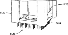
图28A和28B是如本文使用的微孔腔阵列的部分的等比例示图,其示出了圆孔腔和矩形孔腔,以帮助理解阵列结构的三维显象。28A and 28B are isometric views of portions of microwell arrays as used herein, showing circular and rectangular wells to aid in understanding the three-dimensional visualization of the array structure.
图29是显示CMOS芯片上的独立ISFET的阵列的芯片布图的一个角(即左下角)的俯视图的图解说明。Figure 29 is an illustration of a top view showing one corner (ie, lower left) of the chip layout of an array of individual ISFETs on a CMOS chip.
图30是对应于图29中所示的芯片的部分,用于上述传感器阵列的每孔腔一个传感器的实施方案的(典型地为铬)掩模的一部分的布图的实例图解。30 is an illustration of an example layout of a portion of a (typically chrome) mask for a one sensor per cavity embodiment of the sensor array described above, corresponding to the portion of the chip shown in FIG. 29 .
图31是用于每孔腔4个传感器的实施方案的掩模的布图。Figure 31 is a layout of a mask for an embodiment of 4 sensors per cavity.
图32是用于掩蔽围绕阵列的区域,以构建围绕衬底上的传感器的有源阵列的光刻胶的凸缘或壁(或使用地理学意义中的术语:盆形构造)的第二掩模的图解,如图33A中所示。Figure 32 is a second mask used to mask the area around the array to build a lip or wall (or to use the terminology in the geographical sense: basin-shaped configuration) of photoresist around the active array of sensors on the substrate. A diagram of the mold is shown in Figure 33A.
图33是所得的盆形构造的图解。Figure 33 is an illustration of the resulting basin configuration.
图33A是用于制造微孔腔阵列的三层PCM工艺的图解。Figure 33A is an illustration of a three-layer PCM process for fabricating microcavity arrays.
图34-37图解示出将流体界面与传感器阵列合并的合适的试验装置的第一实例,图35提供沿着35-35′线的图34的装置的截面图,且图36是放大了图35的一部分的透视图,图37进一步放大了该结构的一部分以使流体流动变得更直观。Figures 34-37 illustrate a first example of a suitable experimental setup incorporating a fluid interface with a sensor array, Figure 35 provides a cross-sectional view of the device of Figure 34 along line 35-35', and Figure 36 is an enlarged view 35 is a perspective view of a portion of the structure, and Figure 37 further enlarges a portion of the structure to make fluid flow more intuitive.
图38是开始形成特定构造的实例流动腔的具有蚀刻光刻胶层的衬底的示意图。38 is a schematic diagram of a substrate with an etched photoresist layer beginning to form a particular configuration of an example flow chamber.
图39-41是适于制造与图38一致的流动腔的第一构造的掩模的图。39-41 are diagrams of a mask suitable for making a first configuration of a flow chamber consistent with FIG. 38 .
图42-54和57-58是实例装置及其放大的成对局部等比例的截面图,其示出了引入参比电极至流动腔和流动室中的方式和利用诸如塑料和PDMS的材料形成流动腔和流动室。42-54 and 57-58 are example devices and enlarged pairs of partial isometric cross-sectional views thereof showing the manner in which the reference electrode is introduced into the flow chamber and flow chamber and formed using materials such as plastic and PDMS Flow Chambers and Flow Chambers.
图55和56是用于如本文所教导的应用的制造安装在芯片上的流体装置的双层玻璃(或塑料)设置的示意截面图。55 and 56 are schematic cross-sectional views of double glass (or plastic) setups for fabricating on-chip mounted fluidic devices for applications as taught herein.
图59A-59C是用于形成流动腔的两件式注塑件的两个实例的部件的图解。59A-59C are illustrations of components of two examples of a two-piece injection molded part used to form a flow cavity.
图60是将作为电极的不锈钢毛细管引入诸如图59A-59C中的流动腔或其他流动腔的流动腔下游端口的示意截面图。60 is a schematic cross-sectional view of a downstream port of a flow chamber such as that of FIGS. 59A-59C or other flow chambers introducing stainless steel capillaries as electrodes.
图61是示出dNTP并入合成核酸链中伴随无机焦磷酸盐(PPi)释放的示意图。Figure 61 is a schematic diagram showing the incorporation of dNTPs into synthetic nucleic acid strands with the release of inorganic pyrophosphate (PPi).
图62-70示出装载进本发明的微流体阵列的微珠。Figures 62-70 illustrate microbeads loaded into a microfluidic array of the present invention.
图71A是屏幕截图,其示出具有在添加(第一次)dATP导致模板4中的4碱基延伸(参见表1和2)之后出现的信号的像素(左侧的屏幕),以及标以箭头的像素的电压对帧(或时间)的曲线图(右侧的屏幕)。Figure 71A is a screen shot showing pixels (screen on the left) with a signal that appears after addition of (first) dATP resulting in a 4-base extension in template 4 (see Tables 1 and 2), and labeled with Arrow plots pixel voltage versus frame (or time) (right screen).
图71B是屏幕截图,其示出具有在再次添加dCTP导致模板1中的4碱基延伸(参见表1和2)之后出现的信号的像素(左侧的屏幕),以及标以箭头的像素的电压对帧(或时间)的曲线图(右侧的屏幕)。Figure 71B is a screen shot showing pixels with signal that appeared after re-addition of dCTP resulted in a 4-base extension in template 1 (see Tables 1 and 2) (screen on the left), and pixels marked with arrows. Graph of voltage versus frame (or time) (right screen).
图71C是屏幕截图,其示出具有在再次添加dCTP导致模板1、2和4延伸(参见表1和2)之后出现的信号的像素(左侧的屏幕),以及标以箭头的像素的电压对帧(或时间)的曲线图(右侧的屏幕)。Figure 71C is a screen shot showing pixels with signals (left screen) after re-addition of dCTP resulting in extension of
图71D是屏幕截图,其示出具有在添加dTTP并且在所有4个模板中发生全长转录(run-off)(由于存在所有4种dNTP)(参见表1、2)之后出现的信号的像素(左侧的屏幕),以及标以箭头的像素的电压对帧(或时间)的曲线图(右侧的屏幕)。Figure 71D is a screen shot showing pixels with signal appearing after dTTP addition and full-length transcription (run-off) occurs in all 4 templates (due to the presence of all 4 dNTPs) (see Tables 1, 2) (screen on the left), and a graph of voltage versus frame (or time) for pixels marked with arrows (screen on the right).
具体实施方式 Detailed ways
以下内容是涉及与用于分析物检测的大规模化学FET有关的发明方法和装置的各种概念及其实施方案的更详细的说明。应当认识到,上文引入的且在下文更详细说明的各种概念可以任意多种方式来实施,所公开的概念并不限于实施方式任何特定模式。特定实施方式和应用的实例主要用于说明性的目的。The following is a more detailed description of various concepts and embodiments thereof related to the inventive method and apparatus related to large-scale chemical FETs for analyte detection. It should be appreciated that the various concepts introduced above and described in more detail below can be implemented in any number of ways and that the disclosed concepts are not limited to any particular mode of implementation. The examples of specific implementations and applications are presented primarily for illustrative purposes.
根据本公开内容的各个发明实施方案至少部分涉及半导体基/微流体混合系统,其结合了微电子动力和微流体系统的生物相容性。在下文中的某些实例中,为了说明的目的,混合系统的微电子部分由CMOS技术实现。但是应当认识到,本公开内容并不限制在这方面,其他的半导体基技术也可用于实现本文所讨论的系统的微电子部分的各个方面。Various inventive embodiments according to the present disclosure relate, at least in part, to semiconductor-based/microfluidic hybrid systems that combine the power of microelectronics and the biocompatibility of microfluidic systems. In some of the examples below, the microelectronic portion of the hybrid system is implemented in CMOS technology for illustrative purposes. It should be appreciated, however, that the present disclosure is not limited in this respect and that other semiconductor-based technologies may be used to implement various aspects of the microelectronic portion of the systems discussed herein.
本文公开的一个实施方案涉及一种化学敏感场效应晶体管(化学FET)的大规模传感器阵列(例如二维阵列),其中阵列的单个化学FET传感器元件或“像素”设置为检测发生在阵列附近的大量的化学和/或生物学过程(化学反应、细胞培养、神经活动、核酸序列测定过程等)中的分析物浓度的变化。下文详细讨论的各个实施方案所设想的化学FET的实例包括但不限于离子敏感场效应晶体管(ISFET)和酶敏感场效应晶体管(ENFET)。在一个示例性实施方式中,在化学FET传感器阵列上制造一个或多个微流体结构,以为可能生成所感兴趣的分析物的化学反应提供容器和/或密封。例如,在一个实施方式中,微流体结构可构造为设置在阵列的一个或多个传感器上的一个或多个“孔腔”(例如小的反应腔),以使其上设置有给定孔腔的一个或多个传感器检测和测量在给定孔腔中的分析物浓度。One embodiment disclosed herein relates to a large-scale sensor array (e.g., a two-dimensional array) of chemically sensitive field-effect transistors (chemical FETs), wherein individual chemical FET sensor elements or "pixels" of the array are configured to detect Changes in the concentration of analytes in a large number of chemical and/or biological processes (chemical reactions, cell culture, neural activity, nucleic acid sequencing processes, etc.). Examples of chemical FETs contemplated by various embodiments discussed in detail below include, but are not limited to, ion sensitive field effect transistors (ISFETs) and enzyme sensitive field effect transistors (ENFETs). In an exemplary embodiment, one or more microfluidic structures are fabricated on a chemical FET sensor array to provide containment and/or containment for chemical reactions that may generate an analyte of interest. For example, in one embodiment, the microfluidic structure can be configured as one or more "wells" (e.g., small reaction chambers) disposed on one or more sensors of the array such that a given well is disposed thereon. One or more sensors of the lumen detect and measure the analyte concentration in a given lumen.
在某些实施方案中,这种化学FET阵列/微流体混合结构可用于分析包含核酸的感兴趣的溶液/材料。例如,这种结构可用于以大批量序列测定核酸的方式来处理核酸。在不同方面中,这种序列测定可实施来检测核酸序列的同一性,用于核酸片段的单核苷酸同质多晶检测、用于核酸表达谱绘制(在两个或更多状态之间比较核酸表达谱,例如在患病和正常组织之间比较或在未经治疗的组织和用药物、酶、射线或化学处理方式治疗的组织之间比较)、用于单体型(比较存在于人对象中的两等位基因的每一个上的基因和变异基因)、用于染色体组型(识别比较测试组织(典型的是从受孕前的胚胎/胎儿获得以检测出生缺陷)中的一种或多种基因和从“正常”的染色体组型体获得的相同基因)以及用于基因型(比较一个物质的第一个体中的一种或多种基因和相同物质的其他个体中的相同基因)。但是应当认识到,虽然本文公开的概念的某些说明性实例适用于核酸处理范畴,但是本文公开的涉及化学FET传感器阵列的概念的应用并不局限于这些实例。In certain embodiments, such chemical FET array/microfluidic hybrid structures can be used to analyze solutions/materials of interest containing nucleic acids. For example, such structures can be used to process nucleic acids in the manner of sequencing nucleic acids in large batches. In various aspects, such sequencing can be performed to detect nucleic acid sequence identity, for single nucleotide polymorphism detection of nucleic acid fragments, for nucleic acid expression profiling (between two or more states Comparing nucleic acid expression profiles, e.g., between diseased and normal tissue or between untreated tissue and tissue treated with drugs, enzymes, radiation, or chemical treatments), for haplotypes (comparing genes on each of the two alleles and variant genes in human subjects), for karyotype (identification of one of the compared test tissues (typically obtained from pre-conception embryo/fetus to detect birth defects) or genes and the same genes obtained from a "normal" karyotype) and for genotype (comparing one or more genes in the first individual of a substance with the same gene or genes in other individuals of the same substance) Gene). It should be recognized, however, that while certain illustrative examples of the concepts disclosed herein are applicable in the context of nucleic acid processing, the application of the concepts disclosed herein involving chemical FET sensor arrays is not limited to these examples.
图8一般性示出根据本公开内容的一个发明实施方案,包括大规模化学FET阵列的核酸处理系统1000。在以下讨论中,为了说明的目的,将阵列的化学FET传感器描述为对氢离子浓度敏感的ISFET。但是,应当认识到,本公开内容并不限于这个方面,且本文讨论的任何实施方案中的ISFET都用作说明性实例,其他类型的化学FET也可以类似地用于替代性的实施方案中,如下文进一步详细讨论的那样。一方面,系统1000包括半导体/微流体混合结构300,其包括ISFET传感器阵列100和微流体流动腔200。另一方面,流动腔200设置为通过使多个序列测定试剂272(例如基质dATP,dCTP,dGTP,dTTP和其他试剂)可控地进入流动腔来促进设置在流动腔中的核酸模板的序列测定。如图8中所示,序列测定试剂进入到流动腔200可通过由计算机260控制的一个或多个阀270和一个或多个泵274来实现。Figure 8 generally illustrates a nucleic
在图8的系统1000中,根据一个实施方案,ISFET传感器阵列100监测发生在流动腔200的不同部位的pH的变化,这种变化是由一种或多种构成序列测定试剂272的基质和核酸模板之间的化学反应引起的。在下文详细讨论的其他实施方案中,FET传感器阵列可特别地设置成对可以提供与感兴趣的化学反应有关的相关信息的其他分析物具有敏感性。通过阵列控制器250(也受控于计算机260),可以控制ISFET阵列以便获得与分析物测量有关的数据,并且可通过计算机260来处理所采集的数据,以得到与核酸模板的处理有关的有意义的信息。例如,在一个实施方式中,pH的变化量通常与添加到核酸模板的特定类型的基质(例如dATP,dCTP,dGTP,dTTP中的一种)的数量成比例。这种pH的变化可由在给定类型的基质和模板之间反应附近的阵列100的一个或多个ISFET的输出电压的变化来表示。因此,阵列的给定像素的输出信号的电压变化量可用于检测添加到设置在位于给定像素上方的流动腔内的模板中的特定类型的基质的数量。In
一方面,图8中所示的系统1000的流动腔200可以包括设置在ISFET阵列100的相应传感器上的多个孔腔(图8中未示出)。许多技术都可用于将多种处理材料导入这种流动腔的孔腔中。例如,流动腔可以首先装载通过将包含核酸模板的“微珠”离心进孔腔中来进行测序的核酸模板;作为替代方案,这种微珠可以依靠重力而进入孔腔中。在另一实例中,没有使用微珠,而是用一组引物对来覆盖孔腔,并且用适配器将核酸模板提供到流动腔以补足引物对(可将固定材料添加到传感器阵列100或添加到作为芯片封装一部分的分立芯片或可正好在核酸处理之前添加)。包括溶胶凝胶的其他方法可用于将核酸模板固定到ISFET阵列100的表面附近。In one aspect, flow
一旦核酸模板装载进流动腔200的相应孔腔中,接着就可在孔腔中实施桥接扩增,接着通过合成或连接反应来实施产物变性和序列测定。可以预见孔腔中的其他扩增方法(和在孔腔中俘获产物的方法),其包括滚环扩增或其他利用诸如PCR的等温或非等温扩增技术的方法。如图8中所示,包含基质的试剂可导入流动腔(例如通过计算机控制的阀270和泵274),并扩散进孔腔中,或者试剂可通过诸如喷墨打印的其他方法添加到流动腔。在另一实例中,流动腔200可不包含任何孔腔,且可采用试剂的扩散特性来限制ISFET阵列100的各个传感器之间的串扰。Once the nucleic acid templates are loaded into the corresponding wells of the
总之,图8的系统中的流动腔200可采取任意方式设置为在ISFET阵列100附近提供一种或多种分析物;例如,核酸模板(DNA)可直接固定或施加到适当接近传感器阵列100的一个或多个像素的位置处,或在位于传感器阵列上的载体材料(例如一个或多个“微珠”)上。处理试剂(例如酶)还可以直接置于传感器上或阵列附近的一个或多个固相载体上,用于多种生物传感器应用的未使用孔腔或微珠的装置中的酶产生传感器可检测到的产物(例如离子浓度的变化)。In summary, the
对于图8中所示的系统1000的ISFET阵列100来说,一个实施方案中,阵列100是作为利用标准CMOS工艺(例如0.35微米工艺、0.18微米工艺)设计和制造的集成电路而实现的,其包括需要用于检测/测量一种或多种分析物的所有传感器和电子装置。再次参考图1,用于连接ISFET阵列100的一个或多个参比电极76可置于流动腔200中(例如设置在流动腔的“未使用”的孔腔中),或其可暴露于参比物(例如一种或多种序列测定试剂172)以建立基线,以用来比较阵列100的相应ISFET附近的分析物浓度的变化。参比电极76可电连接到阵列100、阵列控制器250或直接连接到计算机260,以利于进行基于从阵列100获得的电压信号的分析物测量;在某些实施方式中,参比电极可连结至电接地或其他预定电位,或者可测量相对于地电位的参比电极电压,从而为ISFET输出信号的测量建立电基准,如下文进一步讨论的那样。For
作为一维或二维阵列,ISFET阵列100并不限于任何特定尺寸,包括少至2-256像素(例如在二维实施方式中的16×16像素)或多至54兆像素(例如在二维实施方式中的7400×7400像素)或更大,且可用于依照本文公开的概念的各种化学/生物检测目的。在图8所示的典型系统的一个实施方案中,阵列的单个ISFET传感器可以设置为对氢离子敏感;但是,还应当认识到本公开内容并不限于这方面,例如ISFET传感器阵列的单个传感器可特别设置为对用于各种应用(例如对公知的诸如钠、银、铁、溴、碘、钙和硝酸盐的其他离子敏感的材料)的其他类型离子浓度具有敏感性。As a one-dimensional or two-dimensional array,
一般地说,根据本公开内容的各个实施方案的化学FET阵列可设置为对各种分析物/化学物质中的任意一种或多种具有敏感性。在一个实施方案中,阵列的一个或多个化学FET可特别设置为对表示一种或多种结合事件(例如与核酸序列测定有关)的一种或多种分析物具有敏感性,且在其他实施方案中,给定阵列的不同化学FET可设置为对不同分析物具有敏感性。例如,在一个实施方案中,阵列的一个或多个传感器(像素)可包括第一类型的化学FET,其设置为对第一分析物化学敏感,而阵列的一个或多个其他传感器包括第二类型的化学FET,其设置为对不同于第一分析物的第二分析物化学敏感。在一个典型实施方式中,第一分析物可以表示与核酸序列测定处理有关的第一结合事件,第二分析物可以表示与核酸序列测定有关的第二结合事件。当然,应当认识到,可以在任何给定阵列中使用多于两种不同类型的化学FET,以检测和/或测量不同类型的分析物/结合事件。通常,应当认识到在本文讨论的传感器阵列的任何实施方案中,给定的传感器阵列可以是“同质”的并且包括用以检测和/或测量相同类型的分析物(例如pH或其他离子浓度)的基本类似或相同类型的化学FET,或者传感器阵列可以是“异质”的并且包括用以检测和/或测量不同类型的分析物的不同类型的化学FET。为了简化所讨论的内容,在下文的传感器阵列的各个实施方案中,再次用ISFET作为实例,但是本公开内容并不限于这方面,并且对于分析物敏感性的几个其他选择将进一步在下文讨论(例如结合图11A)。In general, chemical FET arrays according to various embodiments of the present disclosure can be configured to be sensitive to any one or more of a variety of analytes/chemicals. In one embodiment, one or more chemical FETs of the array may be specifically configured to be sensitive to one or more analytes indicative of one or more binding events (e.g., associated with nucleic acid sequencing), and in other In embodiments, different chemical FETs of a given array can be configured to be sensitive to different analytes. For example, in one embodiment, one or more sensors (pixels) of the array may comprise a first type of chemical FET configured to be chemically sensitive to a first analyte, while one or more other sensors of the array comprise a second A type of chemical FET configured to be chemically sensitive to a second analyte different from the first analyte. In an exemplary embodiment, the first analyte may represent a first binding event associated with nucleic acid sequencing processing, and the second analyte may represent a second binding event associated with nucleic acid sequencing. Of course, it should be appreciated that more than two different types of chemical FETs may be used in any given array to detect and/or measure different types of analytes/binding events. In general, it should be recognized that in any of the embodiments of the sensor arrays discussed herein, a given sensor array may be "homogeneous" and include sensors for detecting and/or measuring the same type of analyte (e.g., pH or other ion concentration). ), or the sensor array may be "heterogeneous" and include different types of chemical FETs to detect and/or measure different types of analytes. To simplify the discussion, in the various embodiments of the sensor array below, ISFETs are again used as an example, but the disclosure is not limited in this respect, and several other options for analyte sensitivity are discussed further below. (eg in conjunction with Figure 11A).
在基于0.35微米CMOS工艺技术(或具有更小特征尺寸的CMOS工艺技术)的典型实施方式中,ISFET阵列100的各个像素可包括ISFET和附属的启用/选择部件,并且可以占据阵列表面上的约十微米乘十微米(即100微米2)或更小的面积;换句话说,可以获得具有约10微米或更小间距(像素到像素的间隔)的阵列。相对于使得像素尺寸至少为12微米或更大的制造ISFET的现有尝试来说,利用0.35微米CMOS工艺技术的约10微米的阵列间距在尺寸缩小方面取得了显著的进步。In a typical implementation based on 0.35 micron CMOS process technology (or CMOS process technology with smaller feature sizes), each pixel of
更具体地说,在根据本公开内容的发明概念在下文进一步讨论的某些实施方案中,约九(9)微米的阵列间距使ISFET阵列可以包括256000以上的像素(即512乘512的阵列),该阵列与相应的行和列选择和偏置/读出电子器件可制造在7毫米乘7毫米的半导体晶片上,而包括四百万个像素(即2048乘2048的阵列,大于4兆像素)的类似传感器阵列可制造在21毫米乘21毫米的半导体晶片上。在其他实例中,约5微米的阵列间距使得ISFET阵列可以包括1.55兆个像素(即1348乘1152的阵列),该阵列与相应的电子部件可制造在9毫米乘9毫米的晶片上,并且包括大于14兆个像素的ISFET传感器阵列和相应的电子部件可制造在22毫米乘20毫米的晶片上。在其他实施方式中,利用小于0.35微米的特征尺寸的CMOS制造工艺(例如0.18微米的CMOS工艺技术)可以制造具有显著低于5微米的间距的ISFET传感器阵列(例如2.6微米的阵列间距或小于8或9微米2的像素面积),其用于非常密集的ISFET阵列。当然,应当认识到,大于10微米的像素尺寸(例如约20、50、100微米或更大)也可在根据本公开内容的化学FET阵列的各个实施方案中实现。More specifically, in certain embodiments discussed further below in accordance with the inventive concepts of the present disclosure, an array pitch of about nine (9) microns allows ISFET arrays to include more than 256,000 pixels (i.e., a 512 by 512 array) , the array, with corresponding row and column selection and biasing/readout electronics, can be fabricated on a 7 mm by 7 mm semiconductor wafer, while comprising four million pixels (i.e., a 2048 by 2048 array, greater than 4 megapixels ) can be fabricated on a 21 mm by 21 mm semiconductor wafer. In other examples, an array pitch of about 5 microns allows an ISFET array to include 1.55 megapixels (i.e., a 1348 by 1152 array), the array and corresponding electronics can be fabricated on a 9 mm by 9 mm wafer, and include An ISFET sensor array of greater than 14 megapixels and corresponding electronics can be fabricated on a 22 mm by 20 mm wafer. In other embodiments, ISFET sensor arrays with pitches significantly below 5 microns (e.g., array pitches of 2.6 microns or less than 8 or 9 micron2 pixel area), which is used for very dense ISFET arrays. Of course, it should be appreciated that pixel sizes greater than 10 microns (eg, about 20, 50, 100 microns or greater) may also be achieved in various embodiments of chemical FET arrays according to the present disclosure.
在图8所示的系统的其他方面中,一个或多个阵列控制器250可用于操纵ISFET阵列100(例如选择/启用阵列的相应像素以获得表示分析物测量的输出信号)。在各个实施方式中,构成一个或多个阵列控制器的一个或多个部件可与这些阵列的像素元件一起实现在与阵列相同的同一集成电路(IC)芯片上但在IC芯片的不同部分中,或者在芯片外实现。就阵列控制而言,ISFET的输出信号的模-数转换可通过在与ISFET阵列相同的集成电路芯片上但位于传感器阵列区域之外实现的电路来实施(将模-数转换电路设置在传感器阵列区域之外获得了更小的间距并因此既实现了更大数量的传感器又降低了噪声)。在下文进一步讨论的各个示例性实施方式中,模-数转换可以是4位、8位、12位、16位或根据所需的信号动态范围的其他的位分辨率。In other aspects of the system shown in FIG. 8, one or
已经提供了用于测量与核酸处理有关的一个或多个分析物的示例性系统1000中的化学FET(例如ISFET)阵列100的一般概述,以下将对根据本公开内容的示例性化学FET阵列进行更详细的说明,该化学FET阵列可用于各种应用中,其包括但不限于核酸处理。此外,为了说明的目的,以下利用ISFET阵列的特定实例来讨论根据本公开内容的化学FET阵列,但其他类型的化学FET也可用于其他实施方案中。Having provided a general overview of a chemical FET (eg, ISFET)
如上所述,本文公开的各个发明实施方案都是特别地针对与图1-7有关的上述Milgrew等人的ISFET阵列设计以及其他现有ISFET阵列设计所作的改进,以便明显降低像素尺寸和阵列间距,且由此对于给定半导体晶片尺寸增加ISFET阵列的像素数量(即像素密度)。在某些实施方式中,在像素密度增加的同时伴随有对应于涉及一种或多种分析物的一种或多种化学性质的相应测量的输出信号的信噪比(SNR)的增加以及可从阵列读取的这种输出信号的速度增加。特别是,申请人已经验证并认识到通过放松对ISFET线性度的要求,而将重点集中在进一步限制信号输出/测量的范围(例如对应于从约7至9而不是1至14的pH范围的信号输出)上,可以显著降低单个像素的复杂度和尺寸,由此有助于实现非常大规模密集的ISFET阵列。As noted above, various inventive embodiments disclosed herein are specific improvements to the ISFET array design of Milgrew et al. described above in relation to FIGS. , and thus increases the number of pixels (ie, pixel density) of the ISFET array for a given semiconductor wafer size. In certain embodiments, an increase in pixel density is accompanied by an increase in the signal-to-noise ratio (SNR) of the output signal corresponding to a corresponding measurement of one or more chemical properties involving one or more analytes and may The speed at which such output signals are read from the array is increased. In particular, Applicants have verified and recognized that by relaxing the ISFET linearity requirements, the focus is on further limiting the range of signal output/measurement (e.g. corresponding to a pH range from about 7 to 9 instead of 1 to 14). Signal output), the complexity and size of a single pixel can be significantly reduced, thereby facilitating the realization of very large-scale dense ISFET arrays.
为此,图9示出了根据本公开内容的一个发明实施方案的ISFET阵列100的一列102j,其中明显简化了ISFET像素设计以利于实现小的像素尺寸。列102j包括n个像素,其中第一和最后一个像素在图9中示出为像素1051和105n。如结合图13在下文进一步讨论的,基于图9中所示的列设计的完整二维ISFET阵列100包括m个这种列102j(j=1,2,3,....m),其一般是并排排列的连续像素列。To this end, FIG. 9 shows a column 102j of an
在图9中所示的实施方案的一个方面中,列102j的像素1051至105n中的每一个仅包括三个部件,即ISFET150(也标记为Q1)和两个MOSFET开关Q2和Q3。MOSFET开关Q2和Q3响应于n个行选择信号(RowSel1至RowSeln,逻辑低激活)中的一个,以启用或选择列102j的一个给定像素。用像素1051作为应用于列的所有像素的实例,在经由线1181接收到相应的行选择信号后,晶体管开关Q3通过线1121将可控电流源106j连接到ISFET150的源极。在接收到相应的行选择信号后,晶体管开关Q2通过线1141将ISFET 150的源极连接到列偏置/读出电路110j。ISFET 150的漏极通过线1161直接连接到偏置/读出电路110j。因此,每个像素只需要四条信号线,即线1121、1141、1161和1181来操作像素1051的三个部件。在m列的阵列中,给定的行选择信号同时施加到各列的一个像素(例如在相应列的相同位置)上。In one aspect of the embodiment shown in FIG. 9 , each of
如图9所示,根据一个实施方案的列102j的设计是基于与图3中所示的Milgrew等人的列设计有关的基本原则。具体而言,当各个像素的ISFET启用时,其设置具有恒定的漏电流IDj和恒定的漏-源极电压VDSj,以便根据上述等式(3)来获得来自于启用像素的输出信号VSj。为此,列102j包括一个可控电流源106j,其连接到模拟电路的正电源电压VDDA且响应于偏压VB1,该偏压VB1由列中的所有像素共享,从而为启用像素的ISFET提供恒定的漏电流IDj。一方面,电流源106j执行实现为电流镜像,其包括两个长沟道长度且高输出阻抗的MOSFET。列还包括偏置/读出电路110j,其也由列中的所有像素共享,以向启用像素的ISFET提供恒定的漏-源极电压。偏置/读出电路110j是基于开尔文电桥构造的,且包括两个运算放大器107A(A1)和107B(A2),上述两个运算放大器设置为缓冲放大器并连接到模拟电路正电源电压VDDA和模拟电源接地电压VSSA。偏置/读出电路还包括可控电流宿108j(类似于电流源106j)和连接二极管的MOSFET Q6,可控电流宿108j连接到模拟接地电压VSSA且响应于偏置电压VB2。设定/控制偏置电压VB1和VB2以协同提供互补源和反向电流。由于电流宿108j拉电流所产生的跨连接二极管的MOSFETQ6的电压被运算放大器强制产生在启用像素的ISFET的漏极和源极两端,成为恒定的漏-源极电压VDSj。As shown in FIG. 9 , the design of columns 102 j according to one embodiment is based on fundamental principles related to the column design of Milgrew et al. shown in FIG. 3 . Specifically, when the ISFET of each pixel is enabled, it is set to have a constant drain current I Dj and a constant drain-source voltage V DSj , so that the output signal V from the enabled pixel is obtained according to the above equation (3). Sj . To this end, column 102 j includes a controllable current source 106 j connected to the analog circuit's positive supply voltage VDDA and responsive to a bias voltage VB1 shared by all pixels in the column, thereby enabling the pixel's ISFET Provides a constant drain current I Dj . In one aspect, the current source 106 j is implemented as a current mirror comprising two MOSFETs with long channel length and high output impedance. The column also includes a bias/
通过在图9的偏置/读出电路110j中使用连接二极管的MOSFETQ6,而不是图3中示出的Milgrew等人的设计中所示的电阻RSDj,从而在CMOS制造工艺中提供了明显的优点。具体而言,匹配电阻一般可以制造为具有约±20%的容错率,然而与CMOS制造工艺匹配的MOSFET的容错率为约±1%或更好。负责提供恒定的ISFET漏-源极电压VDSj的部件的匹配程度可从列到列显著影响从列到列的测量精度(例如偏差)。因此使用MOSFET Q6而不使用电阻明显降低了从列到列的测量偏差。而且,尽管电阻和ISFET的热偏移特性可以略微不同,但是MOSFET和ISFET的热偏移特性即便不是实质上相等也是基本类似的;因此,MOSFET Q6中的任意热偏移实质上消除了ISFET Q1的任意热偏移,这就导致在阵列温度变化时更好的测量稳定性。By using a diode-connected MOSFET Q6 in the bias/readout circuit 110j of FIG. 9 instead of the resistor R SDj shown in the Milgrew et al. design shown in FIG. The advantages. Specifically, matched resistors can generally be fabricated with a tolerance of about ±20%, whereas MOSFETs that are process-matched to CMOS have a tolerance of about ±1% or better. The degree of matching of the components responsible for providing a constant ISFET drain-source voltage V DSj can significantly affect the column-to-column measurement accuracy (eg, skew) from column to column. Therefore using MOSFET Q6 instead of resistors significantly reduces the measurement variation from column to column. Also, although the thermal offset characteristics of resistors and ISFETs can be slightly different, the thermal offset characteristics of MOSFETs and ISFETs are substantially similar if not substantially equal; therefore, any thermal offset in MOSFET Q6 essentially cancels the ISFET Q1 Arbitrary thermal excursions, which result in better measurement stability as the array temperature varies.
图9中,列偏移/读出电路110j还包括采样/保持和缓冲电路,用于提供来自列的输出信号VCOLj。具体而言,在通过各个像素中的晶体管Q2和Q3启用或选择像素1051至105n中的一个之后,放大器107A(A1)的输出,即缓冲的VSj通过响应于列取样和保持信号COL SH的开关(例如传输门电路)操作存储到列取样和保持电容Csh中。用于取样和保持电容的合适电容值的实例包括但不限于从约500fF至2pF的范围。取样电压通过列输出缓冲放大器111j(BUF)被缓冲并提供作为列输出信号VCOLj。还如图9中所示的,基准电压VREF可通过响应于控制信号CAL的开关而施加到缓冲放大器111j,以利于由于缓冲放大器111j造成的列到列的非均匀性的特性化,且因此允许后读出数据校正。In FIG. 9, the column offset/
图9A示出了用于偏置/读出电路110j的放大器107A的其中一个的示例性电路图(与放大器107B的电路图相同),且图9B是放大器107A和107B的放大器偏压对带宽的曲线图。如图9A中所示,放大器107A使用了基于九个MOSFET(M1至M9)的多电流镜像的设置,且设置为统一增益缓冲器,其中放大器的输入和输出分别概括标记为IN+和VOUT。偏压VB4(表示相应的偏置电流)控制放大器的互阻抗并作为带宽控制(即随着电流的增大而增加带宽)。再次参照图9,由于采样和保持电容Csh的存在,当采样和保持开关关闭时,放大器107A的输出实质上驱动滤波器。因此,为了实现可观地高数据速度,可以调节偏压VB4以提供较高的偏置电流并增加放大器带宽。从图9B中可以观察到,在某些示例性实施方式中,可以实现至少40MHz甚至更大的放大器带宽。在某些实施方式中,高达100MHz的放大器带宽可适于容易获得高数据采集速度和相对低的像素采样或“暂停”时间(例如约10至20微秒)。Figure 9A shows an exemplary circuit diagram of one of
在图9中所示的实施方案的另一方面中,与图3中所示的Milgrew等人的像素设计不同的是,像素1051至105n都不包括任何同时需要n沟道和p沟道FET部件的传输门电路或其他器件;具体而言,本实施方案中的像素1051至105n仅包括同一类型(仅为n沟道或仅为p沟道)的FET器件。为了说明的目的,图9中示出的像素1051至105n都表示为仅包括p沟道部件,即两个p沟道MOSFET Q2和Q3以及p沟道ISFET 150。不通过使用传输门电路将ISFET的源极连接到偏置/读出电路110j,这可能会牺牲ISFET输出信号(即ISFET源极电压VS)的某些动态范围。但是,申请人验证并认识到,通过上述潜在的某些输出信号动态范围(由此潜在地限制了给定化学特性例如pH的测量范围),可以消除对各个像素中的不同类型(n沟道和p沟道)的FET器件的需求,且减少了像素部件的数量。如结合附图10-12进一步在下文讨论的,这明显有助于像素尺寸的降低。因此,在一个方面中,这是一种在减小的动态范围和较小的像素尺寸之间有益的权衡。In another aspect of the embodiment shown in FIG. 9 , unlike the Milgrew et al. pixel design shown in FIG. 3 , none of the
在图9所示的实施方案的另一方面中,与Milgrew等人的像素设计不同的是,各个像素1051至105n的ISFET 150都没有将其体连接连接到其源极(即,没有连接ISFET的体连接和源极的电导体,这种电导体迫使ISFET的体连接和源极在工作期间处于相同的电位)。相反,阵列的所有ISFET的体连接都彼此连接且连接到体偏压VBODY。虽然没有在图9中明确示出,但是用于MOSFET Q2和Q3的体连接同样也没有连接到它们各自的源极,而是连接到体偏压VBODY。在基于具有所有p沟道部件的像素的一个示例性实施方式中,体偏压VBODY连接到阵列可具有的最高电压电位(例如VDDA),如结合附图17在下文进一步讨论的那样。In another aspect of the embodiment shown in FIG. 9 , unlike the pixel design of Milgrew et al., none of the
通过将各个ISFET的体连接都不连接到它们的源极,某些非零的源至体电压VSB有可能会产生“体效应”,如结合附图1在上文所讨论的那样,其根据非线性关系而影响ISFET的阈值电压VTH(因此,根据等式(3),会影响诸如pH的化学性质的测量)。但是,申请人已经验证并认识到,通过将重点集中在降低ISFET输出信号的动态范围上,因非零的源至体电压而可能发生在ISFET中的任何体效应都可被相对地最小化。因此,可能导致降低的动态范围的任何测量的非线性度可因不重要而被忽略或予以考虑并补偿(例如通过阵列校准和数据处理技术,如结合图17在下文进一步讨论的那样)。申请人还验证并认识到,通过将各个ISFET的体连接都不连接到它们的源极,构成像素的所有FET都可以共享一个公用的体连接,由此进一步促进像素尺寸的削减,如结合图10-12在下文进一步讨论的那样。因此,在另一方面中,这是一种在减小的动态范围和较小的像素尺寸之间有益的权衡。By not connecting the body connections of the individual ISFETs to their sources, some non-zero source-to-body voltage VSB has the potential to create a "body effect" as discussed above in connection with Figure 1, which The threshold voltage V TH of the ISFET is affected according to a non-linear relationship (thus, according to equation (3), the measurement of a chemical property such as pH is affected). However, applicants have verified and realized that by focusing on reducing the dynamic range of the ISFET output signal, any body effect that may occur in an ISFET due to a non-zero source-to-body voltage can be relatively minimized. Accordingly, any measured non-linearity that may result in reduced dynamic range may be ignored as insignificant or accounted for and compensated for (eg, by array calibration and data processing techniques, as discussed further below in connection with FIG. 17 ). Applicants have also verified and realized that by not connecting the body connections of the individual ISFETs to their sources, all FETs making up a pixel can share a common body connection, thereby further facilitating pixel size reduction, as shown in conjunction with Fig. 10-12 as discussed further below. So, on the other hand, this is a beneficial trade-off between reduced dynamic range and smaller pixel size.
图10示出了根据本公开内容的一个发明实施方案的图9中所示的像素1051的芯片布图设计的俯视图。图11A示出了沿着图10中所示的像素的I-I线的组合截面图,包括在II-II线和III-III线之间的图10右半部的其他元件,其示出像素制造的层叠结构图,并且图12A至12L提供了图11A中所示的各个制造层的俯视图(图12A至12L中的各个图象顺序叠置以形成图10中所示的像素芯片的布图设计)。在一个示例性实施方式中,图10-12中示出的像素设计可利用标准的4-金属、2-多晶硅的0.35微米CMOS工艺来实现,以提供几何正方形的像素,其具有在图10中示出为约9微米的尺寸“e”,以及对应于ISFET的敏感区域的约为7微米的尺寸“f”。FIG. 10 shows a top view of the chip layout of pixel 1051 shown in FIG. 9, according to an inventive embodiment of the present disclosure. Figure 11A shows a combined cross-sectional view along line II of the pixel shown in Figure 10, including other elements in the right half of Figure 10 between lines II-II and III-III, showing pixel fabrication and Figures 12A to 12L provide top views of the various fabrication layers shown in Figure 11A (the images in Figures 12A to 12L are sequentially stacked to form the layout design of the pixel chip shown in Figure 10 ). In one exemplary embodiment, the pixel designs shown in FIGS. 10-12 can be implemented using a standard 4-metal, 2-polysilicon 0.35 micron CMOS process to provide a geometrically square pixel with the Dimension "e" is shown as about 9 microns, and a dimension "f" of about 7 microns corresponds to the sensitive area of the ISFET.
在图10的俯视图中,ISFET 150(在图10中标记为Q1)通常占据了像素图示的右中部,且ISFET的栅极、源极和漏极区域的相应位置表示为Q1G、Q1S和Q1D。MOSFET Q2和Q3通常占据了像素图示的左中部;MOSFET Q2的栅极和源极表示为Q2G和Q2S,MOSFET Q3的栅极和源极表示为Q3G和Q3S。在图10所示的布图的一个方面中,MOSFET Q2和Q3共用漏极,其表示为Q2/3D。在另一方面中,通常从图10的俯视图中可以观察到ISFET形成为其沟道位于沿着像素的第一轴的方向(例如平行于线I-I),而MOSFET Q2和Q3形成为它们的沟道位于沿着垂直于第一轴的第二轴的方向。图10还示出了四条用于操作像素的线,即,连接到Q3的源极的线1121、连接到Q2的源极的线1141、连接到ISFET的漏极的线1161和连接到Q2和Q3的栅极的行选择线1181。参考图9,可以认识到给定列中的所有像素都共用线112、114和116(例如图10中垂直跨过像素的线),且给定行中的所有像素都共用线118(例如图10中水平跨过像素的线);因此,根据图9的像素设计和图10中所示的布图,仅需要四条横跨各个像素的金属线。In the top view of FIG. 10 , ISFET 150 (labeled Q1 in FIG. 10 ) generally occupies the middle right of the pixel illustration, and the corresponding locations of the ISFET's gate, source, and drain regions are indicated as Q1 G , Q1 S and Q1D . MOSFETs Q2 and Q3 typically occupy the middle left of the pixel illustration; the gate and source of MOSFET Q2 are denoted Q2 G and Q2 S , and the gate and source of MOSFET Q3 are denoted Q3 G and Q3 S . In one aspect of the layout shown in Figure 10, MOSFETs Q2 and Q3 share a drain, denoted Q2/ 3D . In another aspect, it can generally be observed from the top view of FIG. 10 that ISFETs are formed with their channels oriented along the first axis of the pixel (e.g., parallel to line II), while MOSFETs Q2 and Q3 are formed with their channels The tracks lie along a direction along a second axis perpendicular to the first axis. Figure 10 also shows four lines for operating the pixels, namely,
现在参考图11A的截面图,n-阱154中的高掺杂p型区域156和158(沿着图10中线I-I设置)构成了ISFET的源极(S)和漏极(D),它们之间设置n-阱的区域160,在该区域中ISFET的p沟道形成在ISFET的多晶硅栅极164和栅极氧化物165下方。根据图10和11中所示的发明实施方案的一个方面,像素1051的所有FET部件都制造为p沟道FET,其形成在p型半导体衬底152中的单一n型阱154中。能够实现这种与Milgrew等人的设计不同的结构是因为,1)在像素中不需要传输门电路;以及2)ISFET的源极没有连接到n-阱的体连接。更具体地说,高掺杂的n型区域162为n-阱154提供了体连接(B),且如图10中所示,体连接B连接到围绕像素1051周边的金属导体322。但是,体连接既没有直接电连接到ISFET的源极区域156(即,没有连接体连接和源极以使它们在工作期间具有相同电位的电导体),也没有直接电连接到像素中任何部件的栅极、源极或漏极。因此,像素的其他p沟道FET部件,即Q2和Q3,可制造在同一n-阱154中。Referring now to the cross-sectional view of FIG. 11A, the highly doped p-
在图11A的组合截面图中,还可观察到对应于MOSFET Q2和Q3的共用漏极(D)的高掺杂p型区域159(沿着图10中的线I-I设置)。为了说明的目的,在图11A中还可观察到MOSFET Q3的多晶硅栅极166,虽然这个栅极没有沿着图10中的线I-I设置,但是其设置在沿着线I-I的截面的“平面之后”。但是,为了简化,图10中所示的MOSFET Q2和Q3的各个源极,以及Q2的栅极都未在图11A中示出,因为它们由于共用漏极因而都沿着相同的轴(即,垂直于图示的平面)设置(如果在图11A中示出它们,则这些元件将使图11A的组合截面图变得非常复杂)。Also visible in the combined cross-sectional view of FIG. 11A is a highly doped p-type region 159 (disposed along line I-I in FIG. 10 ) corresponding to the common drain (D) of MOSFETs Q2 and Q3. For illustrative purposes, also visible in FIG. 11A is the
除图11A中所示的衬底、栅极氧化物和多晶硅层之外,提供多个附加层来为不同的像素部件建立电连接,其包括从中穿过形成导电通孔的交替的金属层和氧化层。根据4-金属CMOS工艺,图11A中的这些层标记为“接触”、“金属1”、“通孔1”、“金属2”、“通孔2”、“金属3”、“通孔3”和“金属4”。为了特别有助于对ISFET的电连接的理解,图11A的组合截面图示出了像素制造的其他元件,这些其他的元件位于图10线II-II和III-III之间的俯视图的右侧。对于ISFET的电连接来说,最上面的金属层304对应于ISFET的敏感区域178,在该敏感区域上设置有分析物敏感的钝化层172。最上面的金属层304以及ISFET的多晶硅栅164和中间导体306、308、312、316、320、326和338一同构成了ISFET的“浮栅”结构170,其模式与在上文讨论的结合图1中所示的常规ISFET设计类似。通过连接到线1161的导体340、328、318、314和310为ISFET的漏极提供电连接。通过导体334和336以及导体324将ISFET的源极连接到MOSFET Q2和Q3的共用漏极(其沿着图10中的线I-I设置)。通过导体330和332将连接到n-阱154的体连接162电连接到“金属1”层上的像素的外周周围的金属导体322。In addition to the substrate, gate oxide, and polysilicon layers shown in FIG. 11A , a number of additional layers are provided to establish electrical connections for the different pixel features, including alternating metal layers through which conductive vias are formed and oxide layer. According to the 4-Metal CMOS process, the layers in Figure 11A are labeled "Contact", "
如上所指出的,图12A至12L提供了图11A中所示的各个制造层的俯视图(图12A至12L中的各个图象顺序叠置形成图10中所示的像素芯片布图设计),图12中,各个层的印有字母的俯视图和图11A的截面图之间的对应关系如下:A)n型阱154;B)注入;C)扩散;D)多晶硅栅极164(ISFET)和166(MOSFET Q2和Q3);E)接触;F)金属1;G)通孔1;H)金属2;I)通孔2;J)金属3;K)通孔3;L)金属4(接触ISFET栅极的顶电极)。图12A至12L中表示的各个附图标记都对应于图11A的组合截面图中存在的相同的部件。As noted above, FIGS. 12A to 12L provide top views of the various fabrication layers shown in FIG. 11A (the individual images in FIGS. 12A to 12L are sequentially stacked to form the pixel chip layout shown in FIG. 12, the corresponding relationship between the lettered top view of each layer and the cross-sectional view of FIG. 11A is as follows: A) n-
因此,图10、11和12A至12L中所示的像素芯片布图设计示出了,根据一个实施方案,相同类型的FET器件可用于像素的所有部件,且所有部件都可以在单一阱中实现。这显著降低了像素所需的面积,由此有助于增加给定区域中的像素密度。Thus, the pixel chip layout designs shown in Figures 10, 11 and 12A to 12L show that, according to one embodiment, the same type of FET device can be used for all components of the pixel, and all components can be implemented in a single well . This significantly reduces the area required for a pixel, thereby helping to increase pixel density in a given area.
在一个示例性实施方式中,ISFET的栅极氧化物165可制造为具有约75埃的厚度,导致每单位面积的栅极氧化物电容Cox为4.5fF/μm2。而且,多晶硅栅极164可制造为具有对应1.2μm的沟道宽度W和从0.35至0.6μm的沟道长度L(即W/L的范围从约2至3.5)的尺寸,且区域160的掺杂可以选择为使得p沟道的载流子迁移率为190cm2/V·s(即1.9E10μm2/V·s)。从上文的等式(2)可知,这导致ISFET的跨导参数β为约170至300μA/V2。在本示例性实施方式的其他方面中,模拟电源电压VDDA为3.3伏特,且偏置VB1和VB2以提供约5μA的恒定ISFET漏电流IDj(在某些实施方式中,可以调整VB1和VB2以提供从约1μA至20μA的漏电流)。而且,MOSFET Q6(参见图9中的偏置/读出电路110j)的尺寸设置为其沟道宽长比(例如W/L为约50)使得在5μA的给定电流IDj下,Q6两端的电压为800mV(即VDSj=800mV)。从等式(3)可知,基于这些示例性参数,这提供了在约0.5至2.5伏特范围内的像素输出电压VSj以及在约0至2伏特范围内的ISFET阈值电压变化。In one exemplary embodiment, the
对于图11A中所示的分析物敏感钝化层172来说,在示例性的CMOS实现过程中,钝化层可特别对氢离子浓度敏感,并且可包括氮化硅(Si3N4)和/或氮氧化硅(Si2N2O)。在常规CMOS工艺中,钝化层可通过一次或多次连续沉积这些材料而形成,且通常用来处理或覆盖器件以保护器件免受污染和增加电稳定性。氮化硅和氮氧化硅所具有的材料性质使得包括这些材料的钝化层提供划伤保护并作为对水和钠的扩散能够起到有效阻挡的阻挡层,而水和钠的扩散会导致器件的金属化结构被腐蚀和/或器件的运行变得不稳定。包括氮化硅和/或氮氧化硅的钝化层还在ISFET器件中提供离子敏感性,这是由于钝化层包含的表面基团可给予或接受来自与其接触的分析物溶液的质子,由此改变了表面电势和器件的阈值电压VX,正如结合图1在上文所讨论的那样。For the analyte-
对于利用铝(其熔点约为650摄氏度)作为金属的CMOS工艺来说,一般通过等离子体增强化学气相沉积(PECVD)来形成氮化硅和/或氮氧化硅的钝化层,其中在250-350摄氏度的辉光放电使得形成氮化硅或氮氧化硅的组分气体被离子化,产生了在晶片表面反应的活性种,从而形成了相应材料的叠层。在一个示例性工艺中,可通过氮氧化硅薄层的初始沉积(约0.2至0.4μm),随后执行氮氧化硅的较厚层的沉积(约0.5μm)以及氮化硅的最后沉积(约0.5μm)来形成具有约1.0至1.5μm厚度的钝化层。因为PECVD工艺中采用低沉积温度,所以铝金属化不会受到不利影响。For the CMOS process using aluminum (its melting point is about 650 degrees Celsius) as the metal, the passivation layer of silicon nitride and/or silicon oxynitride is generally formed by plasma enhanced chemical vapor deposition (PECVD), wherein the passivation layer is formed at 250- The glow discharge at 350 degrees Celsius ionizes the component gases that form silicon nitride or silicon oxynitride, generating active species that react on the wafer surface, thereby forming a stack of corresponding materials. In one exemplary process, an initial deposition of a thin layer of silicon oxynitride (about 0.2 to 0.4 μm), followed by a thicker layer of silicon oxynitride (about 0.5 μm) and a final deposition of silicon nitride (about 0.5 μm) to form a passivation layer having a thickness of about 1.0 to 1.5 μm. Because of the low deposition temperature used in the PECVD process, aluminum metallization is not adversely affected.
但是,申请人已经验证并认识到,虽然低温PECVD工艺为常规CMOS器件提供了充分的钝化,但是低温工艺通常产生低密度且略微多孔的钝化层,其在某些情况下会不利地影响ISFET的阈值电压的稳定性。特别是在ISFET器件的工作期间,随着时间的流逝,低密度多孔钝化层会从溶液中吸附离子并被这些离子所饱和,这进而会导致不希望出现的ISFET阈值电压VTH的时变偏移,从而使精密测量面临挑战。However, applicants have verified and recognized that while low temperature PECVD processes provide adequate passivation for conventional CMOS devices, low temperature processes generally produce low density and slightly porous passivation layers which in some cases can adversely affect ISFET threshold voltage stability. Especially during operation of ISFET devices, over time the low-density porous passivation layer adsorbs ions from solution and becomes saturated with these ions, which in turn leads to an undesired time-varying of the ISFET threshold voltage V offset, making precise measurements challenging.
鉴于上述情况,在一个实施方案中,用金属钨代替铝的CMOS工艺可用来制造根据本公开内容的ISFET阵列。钨的高熔点(3400摄氏度以上)允许使用具有较高温度的低压化学气相沉积(LPCVD)工艺(例如约700至800摄氏度)来制造氮化硅或氮氧化硅钝化层。通常,LPCVD工艺会产生用于钝化层的较大密度和较少孔隙的膜,由此缓解从分析物溶液吸附离子导致ISFET的阈值电压偏移的潜在不利影响。In view of the foregoing, in one embodiment, a CMOS process that substitutes metal tungsten for aluminum may be used to fabricate ISFET arrays according to the present disclosure. The high melting point of tungsten (above 3400 degrees Celsius) allows the use of low pressure chemical vapor deposition (LPCVD) processes with higher temperatures (eg, about 700 to 800 degrees Celsius) to fabricate silicon nitride or silicon oxynitride passivation layers. In general, the LPCVD process results in a denser and less porous film for the passivation layer, thereby mitigating the potential adverse effect of adsorption of ions from the analyte solution leading to a shift in the threshold voltage of the ISFET.
在使用铝基CMOS工艺制造根据本公开内容的ISFET阵列的另一实施方案中,图11A中所示的钝化层172可以包括除用于常规CMOS工艺中的典型的沉积方法和/或材料之外的其他沉积方法和/或材料。例如,钝化层172可包括如上所述的氮化硅和/或氮氧化硅的初始低温等离子体辅助沉积(PECVD);对本讨论内容来说,图11A中说明的这些常规的沉积物作为钝化层172的第一部分172A。在一个实施方案中,第一部分172A形成之后,沉积一种或多种其他钝化材料以形成至少第二部分172B,以增加整个钝化层172的密度并降低孔隙度(和吸附性)。但是所示的附加部分172B主要用于对图11A的说明,应当认识到本公开内容不局限于这方面,因为整个钝化层172可包括两个或多个组成部分,其中各个部分都可包括由相同或不同材料构成的一个或多个层,并且相应的部分可具有相似或不同的结构。In another embodiment in which an ISFET array according to the present disclosure is fabricated using an aluminum-based CMOS process, the
适用于钝化层172的第二部分172B(或其他部分)的对氢离子特别敏感的材料的实例包括但不限于氮化硅、氮氧化硅、氧化铝(Al2O3)、氧化钽(Ta3O5)、氧化锡(SnO2)和二氧化硅((SiO2)。一方面,可通过各种相对低温的工艺来沉积第二部分172B(或其他部分),其包括但不限于RF溅射、DC磁控溅射、热或电子束蒸发和离子辅助沉积。另一方面,可在第二部分172B的沉积之前使用预溅射蚀刻工艺,以移除第一部分172A上的任何天然氧化物(作为替代方案,诸如高温氢氛围的还原性氛围可用于移除第一部分172A上的天然氧化物)。又一方面,如上所述,第二部分172B的厚度可为约0.04μm至0.06μm(400至600埃),且第一部分的厚度可为约1.0至1.5μm。在某些实施方式中,第一部分172A可包括氮氧化硅和氮化硅的多层,该多层的组合厚度为1.0至1.5μm,且第二部分172B可包括氧化铝或氧化钽的单层,该单层厚度约为400至600埃。此外,应当认识到提供上述示例性的厚度主要用于说明的目的,且本公开内容并不限于这些方面。Examples of materials that are particularly sensitive to hydrogen ions suitable for the
因此,可以理解的是,本文说明的化学FET阵列可用于检测多种分析物,且通过这种检测可以监测各种反应和/或相互作用。还可以理解的是,着重于氢离子的检测(以pH的变化的形式进行)是为了简便和简洁起见,其他分析物(包括其他离子)可代替这些说明中的氢。Thus, it will be appreciated that the chemical FET arrays described herein can be used to detect a variety of analytes and that various reactions and/or interactions can be monitored through such detection. It will also be appreciated that the emphasis on detection of hydrogen ions (as a change in pH) is for simplicity and brevity, and that other analytes, including other ions, may be substituted for hydrogen in these illustrations.
本文公开的包括ISFET的化学FET能够检测任何其本身能够诱发电场变化的分析物。分析物无需为了被传感器检测而带电。例如,根据一个实施方案,分析物可以带正电(即阳离子)、带负电(即阴离子)、为两性离子(即能够具有两电量相等且电性相反的电荷,但整体呈电中性)以及为极化但仍呈中性。这个列表并不完备,本领域技术人员根据本文的公开内容可以预期其他分析物质类以及每个种类中的物质。The chemical FETs disclosed herein, including ISFETs, are capable of detecting any analyte that itself induces a change in an electric field. The analyte need not be charged in order to be detected by the sensor. For example, according to one embodiment, the analyte may be positively charged (i.e., a cation), negatively charged (i.e., an anion), zwitterionic (i.e., capable of having two equal and opposite charges, but overall neutral), and polarized but still neutral. This list is not exhaustive, and one of ordinary skill in the art, given the disclosure herein, can contemplate other classes of analytes and substances within each class.
在本发明的最广泛地意义中,钝化层可以覆盖或不覆盖,且分析物可以结合或可以不结合钝化层。作为一个实例,钝化层可由氮化硅构成,且分析物可以是除氢离子外的其他物质。作为一个特定实例,钝化层可由氮化硅构成,且分析物可以是无机焦磷酸盐(PPi)。在这些实例中,直接检测PPi(即,没有直接或间接附着到钝化层的PPi受体)。In the broadest sense of the invention, the passivation layer may or may not be covered, and the analyte may or may not be bound to the passivation layer. As an example, the passivation layer can be composed of silicon nitride, and the analyte can be something other than hydrogen ions. As a specific example, the passivation layer can be composed of silicon nitride and the analyte can be inorganic pyrophosphate (PPi). In these examples, PPi was detected directly (ie, no PPi receptor attached directly or indirectly to the passivation layer).
如果所要检测的分析物是氢(或可替换为氢氧化物),则优选使用弱缓冲剂,以便在钝化层处可检测到离子物质的任何变化。如果所要检测的分析物是除氢(或氢氧化物)以外的其他物质,但在反应或检测步骤期间存在pH变化的某些可能性,则优选使用强缓冲剂,以便pH的变化不会干扰对分析物的检测。缓冲剂是一种抵抗pH变化的离子分子。缓冲剂能够中和添加到或产生于溶液中的酸或碱,这致使溶液中没有显著的pH变化。可以理解的是只要具有所需范围内的pKa,则任意缓冲剂都是适当的。合适的缓冲剂是能在约6至9的pH范围内发挥功能的缓冲剂,且更优选地在6.5至8.5的范围内。缓冲剂的强度是相对的,因为其取决于添加到或产生于感兴趣的溶液中的酸或碱的性质、强度和浓度。弱缓冲剂是一种允许检测(因此不能控制)至少约为+/-0.005、0.01、0.015、0.02、0.03、0.04、0.05、0.10、0.15、0.20、0.25、0.30、0.35、0.45、0.50或更大的pH变化的缓冲剂。在某些实施方案中,pH的变化大约为0.005(例如每个核苷酸合并),且优选为pH增加。强缓冲剂是一种控制至少约为+/-0.005、0.01、0.015、0.02、0.03、0.04、0.05、0.10、0.15、0.20、0.25、0.30、0.35、0.45、0.50或更大的pH变化的缓冲剂。可通过改变缓冲物质本身的浓度来改变缓冲剂强度。因此低浓度缓冲剂可以是低强度缓冲剂。实例包括那些具有小于1mM(例如50-100μM)缓冲物质的缓冲剂。适用于本文说明的读出pH变化的序列测定反应的弱缓冲剂的一个非限制实例是0.1mM Tris或Tricine。实例中提供的可适用的弱缓冲剂的实例在本领域也是公知的。缓冲剂浓度越高则缓冲剂的强度可能越强。其实例包括具有1-25mM缓冲物质的那些。适用于本文说明的PPi直接读出的序列测定反应的强缓冲剂的一个非限制实例是1.5或25mM(或更大)Tris或Tricine。本领域技术人员将能确定用于本发明所涵盖的反应和检测方法的最优缓冲剂。If the analyte to be detected is hydrogen (or alternatively hydroxide), a weak buffer is preferably used so that any change in ionic species is detectable at the passivating layer. If the analyte to be detected is something other than hydrogen (or hydroxide), but there is some possibility of pH change during the reaction or detection steps, it is preferable to use a strong buffer so that the change in pH does not interfere detection of analytes. A buffer is an ionic molecule that resists changes in pH. A buffer is capable of neutralizing acids or bases added to or produced in a solution, which results in no significant pH change in the solution. It will be appreciated that any buffer is suitable as long as it has a pKa in the desired range. A suitable buffer is one that functions in a pH range of about 6 to 9, and more preferably in the range of 6.5 to 8.5. The strength of a buffer is relative in that it depends on the nature, strength and concentration of the acid or base added to or produced in the solution of interest. A weak buffer is one that allows detection (and therefore no control) of at least about +/- 0.005, 0.01, 0.015, 0.02, 0.03, 0.04, 0.05, 0.10, 0.15, 0.20, 0.25, 0.30, 0.35, 0.45, 0.50 or more Buffer for large pH changes. In certain embodiments, the change in pH is about 0.005 (eg, per nucleotide incorporation), and is preferably an increase in pH. A strong buffer is one that controls pH changes of at least about +/- 0.005, 0.01, 0.015, 0.02, 0.03, 0.04, 0.05, 0.10, 0.15, 0.20, 0.25, 0.30, 0.35, 0.45, 0.50, or greater agent. Buffer strength can be varied by varying the concentration of the buffer substance itself. Thus a low concentration buffer may be a low strength buffer. Examples include those with less than 1 mM (eg, 50-100 μM) buffer substance. A non-limiting example of a weak buffer suitable for use in the sequencing reactions described herein to read out the pH change is 0.1 mM Tris or Tricine. Examples of suitable weak buffers provided in the Examples are also well known in the art. The higher the buffer concentration, the stronger the buffer may be. Examples thereof include those with 1-25 mM buffer substances. A non-limiting example of a strong buffer suitable for the sequence determination reaction of the PPi direct readout described herein is 1.5 or 25 mM (or greater) Tris or Tricine. Those skilled in the art will be able to determine optimal buffers for use in the reactions and detection methods encompassed by the present invention.
在某些实施方案中,钝化层和/或覆盖在其上的分子指示出阵列读出装置的分析物特异性。In certain embodiments, the passivation layer and/or the molecules overlying it are indicative of the analyte specificity of the array readout device.
氢离子(以pH的形式)的检测可利用由氮化硅(Si3N4)、氮氧化硅(Si2N2O)、氧化硅(SiO2)、氧化铝(Al2O3)、五氧化二钽(Ta2O5)、氧化锡或二氧化锡(SnO2)等制成的钝化层来实施。Hydrogen ions (in the form of pH) can be detected by silicon nitride (Si 3 N 4 ), silicon oxynitride (Si 2 N 2 O), silicon oxide (SiO 2 ), aluminum oxide (Al 2 O 3 ), The passivation layer made of tantalum pentoxide (Ta 2 O 5 ), tin oxide or tin dioxide (SnO 2 ) etc. is implemented.
钝化层还能直接检测的其他离子物质包括但不限于钙、钾、钠、碘、镁、氯、锂、铅、银、镉、硝酸根、磷酸根、二氢磷酸根等。Other ionic species that the passivation layer can also directly detect include, but are not limited to, calcium, potassium, sodium, iodine, magnesium, chlorine, lithium, lead, silver, cadmium, nitrate, phosphate, dihydrogen phosphate, and the like.
在某些实施方案中,钝化层覆盖有用于所感兴趣的分析物的受体。受体选择性结合目标分析物。如这里使用的,选择性结合分析物的受体是优先结合该分析物(即,其对该分析物的结合亲和力大于其对任何其他分析物的结合亲和力)的分子。其对于目标分析物的结合亲和力可以是对任何其他分析物的结合亲和力的2倍、3倍、4倍、5倍、6倍、7倍、8倍、9倍、10倍、15倍、20倍、25倍、30倍、40倍、50倍、100倍或更大。除其相对结合亲和力之外,受体还必须具有绝对结合亲和力,该绝对结合亲和力是足以有效结合目标分析物的结合亲和力(即,其必须具有足够的灵敏度)。具有在皮摩尔至微摩尔范围内的结合亲和力的受体是适宜的。优选地,这种相互作用是可逆的。In certain embodiments, the passivation layer is covered with receptors for the analyte of interest. The receptor selectively binds the target analyte. As used herein, a receptor that selectively binds an analyte is a molecule that preferentially binds that analyte (ie, has a binding affinity for that analyte that is greater than its binding affinity for any other analyte). Its binding affinity for the target analyte can be 2 times, 3 times, 4 times, 5 times, 6 times, 7 times, 8 times, 9 times, 10 times, 15 times, 20 times the binding affinity for any other analyte times, 25 times, 30 times, 40 times, 50 times, 100 times or more. In addition to its relative binding affinity, the receptor must also have an absolute binding affinity, which is a binding affinity sufficient to efficiently bind the target analyte (ie, it must have sufficient sensitivity). Receptors with binding affinities in the picomolar to micromolar range are suitable. Preferably, this interaction is reversible.
受体可以是任何自然物质(例如,化学物、核酸、肽、脂类、其组合等等)。分析物也可以是任何自然物质,只要存在选择性与其结合且在某些情况下特特异性与其结合的受体即可。但是可以理解的是,本发明还考虑到了在不存在受体的情况下分析物的检测。这样的一个实例是不存在PPi或Pi受体的情况下通过钝化层对PPi和Pi的检测。Receptors can be any natural substance (eg, chemical, nucleic acid, peptide, lipid, combinations thereof, etc.). The analyte can also be any natural substance as long as there are receptors to which it binds selectively and in some cases specifically. It will be appreciated, however, that the invention also contemplates the detection of analytes in the absence of receptors. An example of this is the detection of PPi and Pi through a passivation layer in the absence of PPi or Pi acceptors.
一方面,本发明所关注的受体是离子载体。如这里所使用的,离子载体是一种选择性结合离子物质无论是阳离子或阴离子的分子。在本发明的范畴中,离子载体是受体,与其结合的离子是分析物。本发明的离子载体包括本领域公知的来源于微生物的载流子离子载体(即,结合到特定离子的小脂类可溶分子)。可从例如Calbiochem的来源那里市购各种离子载体。In one aspect, the receptors contemplated by the present invention are ionophores. As used herein, an ionophore is a molecule that selectively binds ionic species, whether cations or anions. In the context of the present invention, ionophores are receptors to which the ions bound are analytes. Ionophores of the present invention include carrier ionophores (ie, small lipid-soluble molecules that bind to specific ions) derived from microorganisms known in the art. Various ionophores are commercially available from sources such as Calbiochem.
可通过利用钝化层本身或通过利用覆盖在钝化层上的受体来实现某些离子的检测。例如,利用聚硅氧烷、缬氨霉素或盐霉素可选择性地检测钾;利用莫能菌素、制霉菌素或SQI-Pr可选择性地检测钠;利用ionomycin、钙霉素(A23187)或CA 1001(ETH 1001)可选择性地检测钙。Detection of certain ions can be achieved by using the passivation layer itself or by using receptors overlying the passivation layer. For example, potassium can be selectively detected using polysiloxanes, valinomycin, or salinomycin; sodium can be selectively detected using monensin, nystatin, or SQI-Pr; ionomycin, calcimycin ( A23187) or CA 1001 (ETH 1001) can selectively detect calcium.
在某些情况下,还可使用能够结合多于一种离子的受体。例如,白僵菌毒素可用于检测钙和/或钡离子,尼日利亚菌素可用于检测钾、氢和/或铅离子,克杀汀(gramicidin)可用于检测氢、钠和/或钾离子。本领域技术人员将能认识到这些化合物可用于不要求单一离子特异性或其中不会(或不可能)存在或产生与化合物结合的其他离子的应用中。In some cases, receptors capable of binding more than one type of ion may also be used. For example, beauveria toxin can be used to detect calcium and/or barium ions, nigericin can be used to detect potassium, hydrogen and/or lead ions, and gramicidin can be used to detect hydrogen, sodium and/or potassium ions. Those skilled in the art will recognize that these compounds are useful in applications that do not require specificity for a single ion or where other ions associated with the compound will not (or cannot) be present or generated.
其他实施方案包括但不限于核酸序列测定应用,可利用选择性结合无机焦磷酸盐(PPi)的受体。PPi受体的实例包括图11B中所示的化合物(化合物1-10)。化合物1记载于Angew Chem Int Ed 200443:4777-4780和US2005/0119497A1中,称为p-萘基-二[(二(2-氮苯基甲基)氨基)甲基]酚。化合物2记载于J Am Chem Soc 2003 125:7752-7753和US2005/0119497A1中,称为p-(p-硝基苯偶氮基)-二[(二(2-氮苯基甲基-1)氨基)甲基]酚(或其双核Zn配合物)。化合物3记载于Sensors and Actuators B199529:324-327中。化合物4记载于Angew Chem Int Ed 200241(20):3811-3814中。化合物5记载于WO 2007/002204中,其中称为二-Zn2+-二吡啶甲基胺(Zn2+-DPA)。化合物1和2的合成方案在US2005/0119497A1中提供并示出。图11C中示出化合物4的示例性合成。图11E中示出化合物10与金属氧化物表面的附着。Other embodiments, including but not limited to nucleic acid sequencing applications, may utilize receptors that selectively bind inorganic pyrophosphate (PPi). Examples of PPi receptors include compounds shown in FIG. 11B (Compounds 1-10).
作为另一实例,用于神经毒素的受体记载于SimonianElectroanalysis 2004,16:1896-1906。As another example, receptors for neurotoxins are described in Simonian Electroanalysis 2004, 16: 1896-1906.
受体可以共价的或非共价的连接到钝化层。受体对钝化层的共价连接可以是直接的或间接的(例如,通过连接剂)。图11D示出利用硅烷醇化学将受体共价结合到钝化层。受体例如可以利用脂族伯胺(左下部)或芳基异硫氰酸盐(右下部)而固定在钝化层上。在这些和其他实施方案中,钝化层本身可由氮化硅、氧化铝、氧化硅、五氧化二钽等构成,并通过其反应表面基团而结合到硅烷层。为了更详细描述用于共价结合到FET表面的硅烷醇的化学处理,至少下列公开内容可作为参考:对于氮化硅来说,参见Sensors and Actuators B 1995 29:324-327,Jpn J Appl Phys 199938:3912-3917 and Langmuir 2005 21:395-402;对于氧化硅来说,参见Protein Sci 1995 4:2532-2544 and Am Biotechnol Lab 2002 20(7):16-18;且对于氧化铝来说,参见Colloids and Surfaces 1992 63:1-9,Sensors andAccuators B 2003 89:40-47,以及Bioconjugate Chem 1997 8:424-433。接着将受体共轭到硅烷化层的反应基团。这种后续的结合可通过利用双官能团连接剂而直接或间接发生,如图11D中所示的那样。双官能团连接剂是一种具有可以结合两个部分的至少两个反应基团的化合物。在某些情况下,反应基团位于连接剂的两端。在某些实施方案中,双官能团连接剂是通用双官能团连接剂,如图11D中示出的那些。通用连接剂是能用于连接多种部分的连接剂。应当认识到图11D中所示的化学处理旨在说明而不是限制。Receptors can be covalently or non-covalently attached to the passivation layer. The covalent attachment of the receptor to the passivation layer can be direct or indirect (eg, via a linking agent). Figure 1 ID shows the covalent attachment of receptors to the passivation layer using silanol chemistry. Receptors can be immobilized on the passivation layer, for example, using primary aliphatic amines (bottom left) or aryl isothiocyanates (bottom right). In these and other embodiments, the passivation layer itself may be composed of silicon nitride, aluminum oxide, silicon oxide, tantalum pentoxide, etc., and bonded to the silane layer through its reactive surface groups. For a more detailed description of the chemical treatment of silanols for covalent bonding to FET surfaces, at least the following publications are referenced: For silicon nitride, see Sensors and Actuators B 1995 29:324-327, Jpn J Appl Phys 199938:3912-3917 and Langmuir 2005 21:395-402; for silica, see Protein Sci 1995 4:2532-2544 and Am Biotechnol Lab 2002 20(7):16-18; and for alumina, See Colloids and Surfaces 1992 63:1-9, Sensors and Accuators B 2003 89:40-47, and Bioconjugate Chem 1997 8:424-433. The acceptor is then conjugated to the reactive group of the silylated layer. This subsequent conjugation can occur directly or indirectly through the use of bifunctional linkers, as shown in Figure 11D. A bifunctional linker is a compound having at least two reactive groups that can join two moieties. In some cases, reactive groups are located on both ends of the linker. In certain embodiments, the bifunctional linker is a universal bifunctional linker, such as those shown in Figure 11D. A universal linker is a linker that can be used to link multiple moieties. It should be appreciated that the chemical treatments shown in Figure 11D are intended to be illustrative and not limiting.
双官能团连接剂可以是同质双官能团连接剂或异质双官能团连接剂,这取决于所要结合的分子的性质。同质双官能团连接剂具有两个相同的反应基团。异质双官能团连接剂具有两个不同的反应基团。可市购的各种连接剂可与下列基团的一种或多种反应:伯胺、仲胺、巯基、羧基、羰基和烃。胺特异性连接剂的实例是辛二酸二(硫代琥珀酰亚胺)酯、二[2-(琥珀酰亚胺氧基羰氧基)乙基]砜、辛二酸二琥珀酰亚胺酯、酒石酸二琥珀酰亚胺酯、二亚胺代己二酸二甲酯二盐酸盐(dimethyl adipimate·2HCl)、庚二亚氨酸二甲酯二盐酸盐、辛二亚氨酸二甲酯二盐酸盐和双-[琥珀酰亚胺基-[琥珀酸]]乙二醇酯。可与巯基反应的连接剂包括二马来酰亚胺基己烷、1,4-二-[3′-(2′-吡啶基二硫基)-丙酰胺基)]丁烷、1-[p-叠氮基水杨酰胺基]-4-[碘代乙酰胺基]丁烷以及N-[4-(p-叠氮基水杨酰胺基)丁基]-3′-[2′-吡啶基二硫基]丙酰胺。优先与烃发生反应的连接剂包括叠氮基苯甲酰肼。优选地,优先与羧基发生反应的连接剂包括4-[p-叠氮基水杨酰胺基]丁胺。The bifunctional linker can be a homobifunctional linker or a heterobifunctional linker, depending on the nature of the molecules to be joined. Homobifunctional linkers have two identical reactive groups. A heterobifunctional linker has two different reactive groups. A variety of linkers are commercially available that react with one or more of the following groups: primary amines, secondary amines, thiols, carboxyls, carbonyls, and hydrocarbons. Examples of amine-specific linkers are bis(thiosuccinimide) suberate, bis[2-(succinimidyloxycarbonyloxy)ethyl]sulfone, disuccinimide suberate Esters, disuccinimidyl tartrate, dimethyl adipimate dihydrochloride (dimethyl adipimate 2HCl), dimethyl adipic acid dihydrochloride, suberimidic acid dihydrochloride Methyl ester dihydrochloride and bis-[succinimidyl-[succinic acid]]ethylene glycol ester. Linkers reactive with sulfhydryl groups include dimaleimidohexane, 1,4-bis-[3'-(2'-pyridyldithio)-propionamido)]butane, 1-[ p-Azidosalicylamido]-4-[iodoacetamido]butane and N-[4-(p-azidosalicylamido)butyl]-3′-[2′- Pyridyldithio]propionamide. Linking agents that react preferentially with hydrocarbons include azidobenzohydrazide. Preferably, linkers that preferentially react with carboxyl groups include 4-[p-azidosalicylamido]butylamine.
与胺和巯基反应的异质双官能团连接剂包括丙酸N-琥珀酰亚胺基-3-[2-吡啶基二硫基]脂、[4-碘代乙酰]氨基苯甲酸琥珀酰亚胺酯、4-[N-马来酰亚胺基甲基]环己烷-1-羧酸琥珀酰亚胺酯、m-马来酰亚胺基苯甲酰基-N-羟基琥珀酰亚胺脂、6-[3-[2-吡啶基二硫基]丙酰胺基]己酸硫代马来酰亚胺酯和4-[N-马来酰亚胺基甲基]环己烷-1-羧酸硫代马来酰亚胺酯。与羧基和胺基反应的异质双官能团连接剂包括1-乙基-3-[3-二甲基氨丙基]碳二亚胺盐酸盐。与烃和巯基反应的异质双官能团连接剂包括4-[N-马来酰亚胺基甲基]环己烷-1-羧基酰肼二盐酸盐、4-(4-N-马来酰亚胺基苯基)丁酸酰肼二盐酸盐和3-[2-吡啶基二硫基]丙酰肼。Heterobifunctional linkers reactive with amines and thiols include N-succinimidyl-3-[2-pyridyldithio]propionate, succinimidyl [4-iodoacetyl]aminobenzoate Ester, 4-[N-Maleimidomethyl]cyclohexane-1-carboxylic acid succinimidyl ester, m-maleimidobenzoyl-N-hydroxysuccinimide ester , 6-[3-[2-pyridyldithio]propionamido]hexanoic acid thiomaleimide ester and 4-[N-maleimidomethyl]cyclohexane-1- Thiomaleimide Carboxylate. Heterobifunctional linkers reactive with carboxyl and amine groups include 1-ethyl-3-[3-dimethylaminopropyl]carbodiimide hydrochloride. Heterobifunctional linkers reactive with hydrocarbons and thiols include 4-[N-maleimidomethyl]cyclohexane-1-carboxyhydrazide dihydrochloride, 4-(4-N-maleimido Imidophenyl) butyric acid hydrazide dihydrochloride and 3-[2-pyridyldithio]propionyl hydrazide.
作为替代方案,受体可以是非共价地覆盖在钝化层上。受体在钝化层上非共价沉积可以包括利用聚合物母体。聚合物可以天然存在或非天然存在,且可以包括但不限于核酸(例如DNA、RNA、PNA、LNA等或其模拟物、衍生物或其组合)、氨基酸(例如缩氨酸、蛋白质(天然的或变性的)等,或者其模拟物、衍生物或其组合)、类脂、多糖和功能化嵌段共聚物的任何类型。受体可吸附在聚合母体上和/或嵌入在聚合母体内。Alternatively, the acceptor can be non-covalently coated on the passivation layer. Non-covalent deposition of acceptors on the passivation layer may involve the use of polymeric precursors. Polymers can be naturally occurring or non-naturally occurring, and can include, but are not limited to, nucleic acids (e.g., DNA, RNA, PNA, LNA, etc., or mimetics, derivatives, or combinations thereof), amino acids (e.g., peptides, proteins (natural or denatured), etc., or their mimetics, derivatives or combinations thereof), lipids, polysaccharides and any type of functionalized block copolymers. The receptors can be adsorbed on and/or embedded within the polymeric matrix.
作为替代方案,受体可共价共轭或交联到聚合物(例如,其可以“接枝”到功能化聚合物上)。Alternatively, the receptor can be covalently conjugated or cross-linked to the polymer (eg, it can be "grafted" onto the functionalized polymer).
合适的缩氨酸聚合物的一个实例是聚赖氨酸(例如聚左旋赖氨酸)。其他聚合物的实例包括嵌段共聚物,其包括聚乙二醇(PEG)、聚酰胺、聚碳酸酯、聚环烷、聚亚烷基二醇、聚环氧烷、聚对苯二甲酸亚烷基二醇酯、多乙烯醇、聚乙烯基醚、聚乙烯酯、聚卤乙烯、聚乙烯吡咯烷酮、聚二醇、聚硅氧烷、聚氨酯、烷基纤维素、羟烷基纤维素、纤维素醚、纤维素酯、硝基纤维素、丙烯酸和甲基丙烯酸酯的聚合物、甲基纤维素、乙基纤维素、羟丙基纤维素、羟丙甲基纤维素、羟丁甲基纤维素、乙酸纤维素酯、丙酸纤维素酯、丁酸乙酸纤维素酯、邻苯二甲酸乙酸纤维素酯、羧乙基纤维素、三乙酸纤维素酯、纤维素硫酸钠盐、聚(甲基丙烯酸甲酯)、聚(甲基丙烯酸乙酯)、聚(甲基丙烯酸丁酯)、聚(甲基丙烯酸异丁酯)、聚(甲基丙烯酸己酯)、聚(甲基丙烯酸异癸酯)、聚(甲基丙烯酸月桂酯)、聚(甲基丙烯酸苯酯)、聚(丙烯酸甲酯)、聚(丙烯酸异丙酯)、聚(丙烯酸异丁酯)、聚(丙烯酸十八烷基酯)、聚乙烯、聚丙烯、聚(乙二醇)、聚(环氧乙烷)、聚(对苯二甲酸乙二醇酯)、聚(乙烯醇)、聚乙酸乙烯酯、聚氯乙烯、聚苯乙烯、聚透明质酸、酪朊、凝胶、明胶、聚酐、聚丙烯酸、藻酸盐、壳聚糖、聚(甲基丙烯酸甲酯)、聚(甲基丙烯酸乙酯)、聚(甲基丙烯酸丁酯)、聚(甲基丙烯酸异丁酯)、聚(甲基丙烯酸己酯)、聚(甲基丙烯酸异癸酯)、聚(甲基丙烯酸月桂酯)、聚(甲基丙烯酸苯酯)、聚(丙烯酸甲酯)、聚(丙烯酸异丙酯)、聚(丙烯酸异丁酯)、聚(丙烯酸十八烷基酯)、聚(丙交酯-乙交酯)、草酸盐共聚物、聚己内酯、聚酯酰胺、聚原酸酯、聚羟基丁酸、聚酐、聚(苯乙烯-嵌段-异丁烯-嵌段-苯乙烯)(SIBS)嵌段共聚物、乙烯醋酸乙烯酯、聚(甲基)丙烯酸、乳酸和乙醇酸的聚合物、聚酐、聚(原酸)酯、聚氨酯、聚(丁酸)、聚(戊酸)、和聚(丙交酯-己内酯),和天然聚合物如藻酸盐,以及其他多糖包括葡聚糖和纤维素、胶原蛋白、白蛋白、和其他亲水蛋白质、玉米蛋白和其他醇溶谷蛋白和疏水蛋白质、共聚物和其混合物,及其化学衍生物包括化学基团的取代和/或添加,例如烷基化、亚烷基化、羟基化、氧化和其他本领域技术人员进行的常规改性。One example of a suitable peptide polymer is polylysine (eg, poly-L-lysine). Examples of other polymers include block copolymers including polyethylene glycol (PEG), polyamides, polycarbonates, polycycloalkanes, polyalkylene glycols, polyalkylene oxides, polyethylene terephthalates Alkyl glycol ester, polyvinyl alcohol, polyvinyl ether, polyvinyl ester, polyvinyl halide, polyvinyl pyrrolidone, polyglycol, polysiloxane, polyurethane, alkyl cellulose, hydroxyalkyl cellulose, fiber Vegetable ethers, cellulose esters, nitrocellulose, polymers of acrylic acid and methacrylate esters, methyl cellulose, ethyl cellulose, hydroxypropyl cellulose, hydroxypropyl methyl cellulose, hydroxybutyl methyl cellulose, Cellulose acetate, cellulose propionate, cellulose acetate butyrate, cellulose acetate phthalate, carboxyethyl cellulose, cellulose triacetate, cellulose sulfate sodium salt, poly(methacrylic acid methyl ester), poly(ethyl methacrylate), poly(butyl methacrylate), poly(isobutyl methacrylate), poly(hexyl methacrylate), poly(isodecyl methacrylate) , poly(lauryl methacrylate), poly(phenyl methacrylate), poly(methyl acrylate), poly(isopropyl acrylate), poly(isobutyl acrylate), poly(octadecyl acrylate) ), polyethylene, polypropylene, poly(ethylene glycol), poly(ethylene oxide), poly(ethylene terephthalate), poly(vinyl alcohol), polyvinyl acetate, polyvinyl chloride, Polystyrene, polyhyaluronic acid, casein, gelatin, gelatin, polyanhydrides, polyacrylic acid, alginate, chitosan, poly(methyl methacrylate), poly(ethyl methacrylate), poly (butyl methacrylate), poly(isobutyl methacrylate), poly(hexyl methacrylate), poly(isodecyl methacrylate), poly(lauryl methacrylate), poly(methacrylate phenyl acrylate), poly(methyl acrylate), poly(isopropyl acrylate), poly(isobutyl acrylate), poly(octadecyl acrylate), poly(lactide-glycolide), straw Polyester copolymer, polycaprolactone, polyesteramide, polyorthoester, polyhydroxybutyrate, polyanhydride, poly(styrene-block-isobutylene-block-styrene) (SIBS) block copolymer , ethylene vinyl acetate, poly(meth)acrylic acid, polymers of lactic and glycolic acids, polyanhydrides, poly(ortho)esters, polyurethanes, poly(butyric acid), poly(valeric acid), and poly(lactate ester-caprolactone), and natural polymers such as alginate, and other polysaccharides including dextran and cellulose, collagen, albumin, and other hydrophilic proteins, zein and other prolamins, and hydrophobic proteins , copolymers and mixtures thereof, and chemical derivatives thereof include substitution and/or addition of chemical groups such as alkylation, alkylene, hydroxylation, oxidation and other conventional modifications performed by those skilled in the art.
与ISFET的阈值电压稳定性和/或可预见性有关的另一问题包括俘获电荷会在用CMOS工艺制造的金属层上积累,这是由于阵列制造期间或之后的各种工艺活动(例如生产线后段工艺,例如等离子体金属蚀刻、晶片清洗、切割、封装、输送等)造成的。特别是,参照图11A,在某些情况下,俘获电荷会在构成ISFET浮栅结构170的一个或多个不同导体304、306、308、312、316、320、326、338和164上积累。这种现象在有关文献中还称作“天线效应”。Another issue related to the threshold voltage stability and/or predictability of ISFETs includes the accumulation of trapped charges on metal layers fabricated in CMOS processes due to various process activities during or after array fabrication (e.g., post-line process, such as plasma metal etching, wafer cleaning, dicing, packaging, transportation, etc.). In particular, referring to FIG. 11A , in some cases, trapped charge can accumulate on one or more of the
积累俘获电荷的一个机会包括最顶端金属层304的等离子体蚀刻。申请人已经验证并认识到俘获电荷在浮栅结构的一个或多个导体上积累的其他机会包括期间切割晶片的划片机的研磨过程会产生静电的晶片切割和/或各个后处理晶片输送/封装步骤,其中装卸/输送晶片的自动化机械可以是对浮栅结构的导体静电放电(ESD)的来源。如果没有为硅衬底(或其他半导体衬底)提供连接以构成移除这种电荷积聚的电通路,则电荷会增加到导致栅极氧化物165发生不期望的变化或损坏的程度(例如电荷注入进氧化物或击穿低级氧化物到达下方衬底)。栅极氧化物中或栅极氧化物-半导体界面处的俘获电荷还会导致不期望的和/或不可预见的ISFET操作和性能的变化。One opportunity to accumulate trapped charge includes plasma etching of the
考虑到上述原因,本公开内容的其他发明实施方案涉及通过减少俘获电荷或缓解天线效应而提升ISFET性能的方法和装置。在一个实施方案中,可在传感器阵列制造完成之后减少俘获电荷,而在其他实施方案中,可以改进制造工艺本身来减少由某些常规工艺步骤感生的俘获电荷。在另外的实施方案中,可以组合使用“制造期间”和“后制造”技术来减少俘获电荷,且由此提升ISFET的性能。With the foregoing in mind, other inventive embodiments of the present disclosure relate to methods and apparatus for enhancing ISFET performance by reducing trapped charge or mitigating antenna effects. In one embodiment, trapped charge can be reduced after sensor array fabrication is complete, while in other embodiments, the fabrication process itself can be modified to reduce trapped charge induced by certain conventional process steps. In further embodiments, "during fabrication" and "post fabrication" techniques may be used in combination to reduce trapped charge and thereby improve ISFET performance.
对于改变制造工艺本身而减少俘获电荷来说,在一个实施方案中,可以特定地选择图11A中所示的栅极氧化物165的厚度,以利于移除衬底的积累电荷;特别是,较薄的栅极氧化物会使大量产生的电荷穿过栅极氧化物直至其下的衬底而不被俘获。在根据这种观点的另一实施方案中,可将像素设计为包括一个额外的“牺牲”器件,即,具有比ISFET的栅极氧化物165还薄的栅极氧化物的另一晶体管。然后,ISFET的浮栅结构可连接到牺牲器件的栅极,以使其用为“电荷移除晶体管”。当然,应当认识到某些包括这种牺牲器件的折中方案包括增加像素尺寸和复杂度。For changing the manufacturing process itself to reduce trapped charges, in one embodiment, the thickness of the
在另一实施方案中,在等离子体蚀刻之前,可用电介质覆盖图11A中所示的ISFET浮栅结构170的最顶端金属层304,以减少俘获电荷。如上所述,在某些情况下,浮栅结构上积累的电荷与用于金属蚀刻的等离子体有关。通常,光刻胶施加到待蚀刻的金属上,接着根据下方金属的所需几何图形而被图案化。在一个示例性实施方式中,在光刻胶施加之前,覆盖介电层(例如氧化物)可沉积到待蚀刻的金属上,以在金属表面提供用来阻挡等离子蚀刻工艺产生的电荷的一个额外的阻挡层。一方面,覆盖介电层可在后续工艺中继续保留,且其构成钝化层172的一部分。In another embodiment, the
在另一实施方案中,用于最顶端金属层304的金属蚀刻工艺可改进为包括湿化学或离子束研磨,而不是等离子蚀刻。例如,可用对下方电介质具有选择性的水性化学处理来蚀刻金属层304(例如参见http://www.transene.com/aluminum.html,在此其全部内容通过引用并入本文)。另一替代方法是对金属层304使用离子研磨而不是等离子体蚀刻。离子研磨通常用于蚀刻不能容易地利用常规等离子体或湿化学处理移除的材料。离子研磨工艺不使用等离子体工艺中的振荡电场,因此不会在金属层中产生电荷。另一金属蚀刻替代方法包括最优化等离子体条件以降低蚀刻速度(即较小的功率密度)。In another embodiment, the metal etch process for the
在另一实施方案中,可以改变金属层的构造以利于在制造浮栅期间完全电绝缘。一方面,将金属设计为层叠的,以便大面积ISFET浮栅在其可能需要作为“跳线”的后续金属层以实现对晶体管浮栅的电连接的最终制造期间没有连接任何结构。这种“跳线”连接设计避免了电荷从大的浮栅流至晶体管。这种方法可通过以下步骤实现(M=金属层):i)M1接触多晶硅栅电极;ii)M2接触M1;iii)M3限定浮栅且利用隔离岛与M2断开连接;iv)具有非常小的面积的M4跳线,其在隔离岛上被蚀刻且连接浮栅M3,将M3浮栅连接到与正好在晶体管有源区域上的多晶硅栅连接的M1/M2/M3叠层;以及v)仅移除浮栅上的M3和M4之间的层间电介质,以便暴露出裸露的M3浮栅。在上述方法概述中,可以不需要实施步骤v),因为根据上文讨论的某些实施方案的ISFET构造将M4的钝化层留在M4的浮栅上。一方面,移除仍然可以在其他方面提升ISFET的性能(即灵敏度)。总之,最终形成的化学敏感钝化层可以是薄的溅射沉积离子敏感金属氧化物层。应当认识到上文讨论的表层跳线构造可以在标准CMOS制造流程中实现,从而使得最初的三个金属层中的任意金属层用作浮栅(即M1、M2或M3)。In another embodiment, the configuration of the metal layer can be altered to facilitate complete electrical isolation during fabrication of the floating gate. On the one hand, the metal is designed to be stacked so that the large area ISFET floating gate is not connected to any structure during its final fabrication which may require subsequent metal layers as "jumpers" to make electrical connections to the transistor floating gate. This "jumper" connection design prevents charge from flowing from the large floating gate to the transistor. This approach can be achieved by the following steps (M = metal layer): i) M1 contacts the polysilicon gate electrode; ii) M2 contacts M1; iii) M3 defines a floating gate and is disconnected from M2 by an isolation island; iv) has a very small M4 jumper of the area of , which is etched on the isolation island and connects the floating gate M3, which connects the M3 floating gate to the M1/M2/M3 stack connected to the polysilicon gate just above the transistor active area; and v) Only the interlayer dielectric between M3 and M4 on the floating gate is removed to expose the bare M3 floating gate. In the above method overview, it may not be necessary to perform step v) because the ISFET configuration according to certain embodiments discussed above leaves the passivation layer of M4 on the floating gate of M4. On the one hand, removal can still improve the ISFET's performance (ie, sensitivity) in other ways. In conclusion, the final chemically sensitive passivation layer can be a thin sputter-deposited ion-sensitive metal oxide layer. It should be appreciated that the surface jumper configuration discussed above can be implemented in a standard CMOS fabrication flow such that any of the first three metal layers are used as floating gates (ie M1, M2 or M3).
对于减少俘获电荷的后制造工艺来说,在一个实施方案中,“合成气体退火”可用作后制造工艺,以减小俘获电荷的潜在的不利影响。在合成气体退火中,在氢气和氮气混合物的氛围下热处理由CMOS制造的ISFET器件。混合物中的氢气扩散进栅极氧化物165且中和特定形式存在的俘获电荷。一方面,合成气体退火没必要解决由俘获电荷造成的所有栅极氧化物损伤;而是在某些情况下,对某些俘获电荷的部分中和已经足以显著提升ISFET的性能。在根据本公开内容的示例性退火处理中,ISFET可在包括10%至15%的氢气的氢/氮混合气体中,在400至425摄氏度下热处理约30至60分钟。在一个特定的实施方式中,在包括10%的氢气的氢/氮混合气体中,在425摄氏度下热处理约30分钟,可以观察到对提升ISFET的性能特别有效。对于铝CMOS工艺来说,退火温度应保持在450摄氏度或低于该温度,以避免破坏铝冶金性。在根据本公开内容的退火工艺的另一方面中,在切割制造好ISFET阵列的晶片之后实施合成气体退火,以便确保可有效地改善因为切割工艺本身引起的俘获电荷和/或其他预切割工艺步骤(例如金属的等离子体蚀刻)而造成的缺陷。For post-manufacturing processes to reduce trapped charge, in one embodiment, a "forming gas anneal" may be used as a post-manufacturing process to reduce the potential adverse effects of trapped charges. In forming gas annealing, ISFET devices fabricated from CMOS are thermally treated in an atmosphere of a mixture of hydrogen and nitrogen. The hydrogen gas in the mixture diffuses into the
在根据本公开内容的实施方案的用于减小俘获电荷潜在不利影响的另外的工艺中,可在任意多种晶片后制造输送/封装步骤期间采用各种“静电放电(ESD)-敏感方案”。例如,在一个示例性工艺中,可以使用抗静电切割带来将晶片衬底固定在适当位置(例如切割处理期间)。而且,虽然高电阻率(例如10MΩ)的去离子水通常使用在划片机的冷却中,但是根据本公开内容的一个实施方案,较小电阻率/较大传导性的水可用于此目的,以利于电荷经水传导;例如,可用二氧化碳来处理去离子水,以降低电阻率并提高对于切割工艺所产生电荷的传导性。而且,可在各个晶片切割/输送/封装步骤期间使用具有良好接地的晶片弹出工具,再次为任意这些步骤中所产生的电荷提供有效的传导路径,由此减小阵列的各个ISFET的浮栅结构的一个或多个导体上积累电荷的机会。In an additional process for reducing the potential adverse effects of trapped charges according to embodiments of the present disclosure, various "electrostatic discharge (ESD)-sensitive schemes" may be employed during any of a variety of post-wafer manufacturing transport/packaging steps . For example, in one exemplary process, an antistatic dicing tape may be used to hold the wafer substrate in place (eg, during the dicing process). Also, while high resistivity (eg, 10 MΩ) deionized water is commonly used in the cooling of dicing machines, according to one embodiment of the present disclosure, less resistivity/more conductive water can be used for this purpose, To facilitate charge conduction through water; for example, deionized water can be treated with carbon dioxide to reduce resistivity and increase conductivity for charges generated by the dicing process. Also, a wafer eject tool with good grounding can be used during the various wafer dicing/transporting/packaging steps, again providing an efficient conduction path for the charges generated during any of these steps, thereby reducing the floating gate structure of the individual ISFETs of the array The opportunity for charge to accumulate on one or more conductors.
在涉及减少俘获电荷的后制造工艺的另一实施方案中,可用UV辐射来照射ISFET的栅极氧化物区域。再次参考图11A,在基于本实施方案的一个示例性实施方式中,在ISFET阵列的制造过程中,阵列的各个像素的顶金属层304中可包括一个任选的孔或窗口302,其接近ISFET的浮栅结构。当UV辐射产生时,这个窗口旨在将UV辐射引入ISFET的栅极区域;特别是,如图11和12A-L中所示的像素1051的各个层设置为使进入窗口302的UV辐射得以基本无阻碍地撞击多晶硅栅极164和栅极氧化物165附近的区域。In another embodiment involving post-manufacturing processing to reduce trapped charge, the gate oxide region of the ISFET may be irradiated with UV radiation. Referring again to FIG. 11A , in an exemplary embodiment based on this embodiment, during the fabrication of the ISFET array, an optional hole or
为了利于降低俘获电荷的UV辐射工艺,申请人已经验证并认识到通常需要在图11A中所示的钝化层172中使用除氮化硅和氮氧化硅外的其他材料,这是因为氮化硅和氮氧化硅严重吸收UV辐射。鉴于上述问题,这些材料需要被其他对UV辐射非常透明的材料替换,这些可替换的材料的实例包括但不限于磷硅酸盐玻璃(PSG)和硼掺杂磷硅酸盐玻璃(BPSG)。但是PSG和BPSG能透过氢和氢氧离子;因此,为了使其能够使用在对pH敏感的ISFET设计的钝化层中,PSG和BPSG可与离子可透过材料一同使用而形成钝化层,该离子可透过材料例如氧化铝(Al2O3)也对UV辐射非常透明。例如,再次参考图11A,可在钝化层172的第一区域172A中使用PSG或BPSG来代替氮化硅或氮氧化硅,并可在钝化层172的第二部分172B中使用氧化铝薄层(例如400至600埃)(例如,可利用后CMOS剥离光刻工艺来沉积氧化铝)。In order to facilitate a UV radiation process that reduces trapped charge, applicants have verified and realized that it is generally desirable to use materials other than silicon nitride and silicon oxynitride in the
在包括UV辐射的实施方案的另一方面中,传感器阵列的各个ISFET必须在UV辐射处理期间适当地偏置,以利于俘获电荷的减少。特别地,撞击其中形成ISFET的传导沟道的本体硅区域160的来源于UV辐射的高能光子产生电子空穴对,其有助于在电流流过ISFET的传导沟道时中和栅极氧化物中的俘获电荷。为此,结合图17在下文进一步讨论的阵列控制器在UV辐射处理期间产生适当的用于偏置阵列的ISFET的信号。特别地,再次参考图9,产生RowSel1至RowSeln的各个信号以便同时启用/选择(即开启)传感器阵列的所有行,且由此将阵列的所有ISFET连接至各个列中的相应的可控电流源106j。随着各个列的所有像素同时被选择,来自给定列的电流源106j被列中的所有像素所共享。通过移除偏置电压VB4而关闭列放大器107A和107B,同时,通过对应于控制信号“UV”的开关将连接到给定列中的各个ISFET的漏极的放大器107B的输出接地。而且,用于阵列的所有ISFET的共用体电压VBODY连接到电接地(即VBODY=0伏特)(如上所述,在阵列的一般操作中,体偏置电压VBODY连接到可用于阵列的最高电压电位,例如VDDA)。在一个示例性过程中,用于所有可控电流源106j的偏置电压VB1设置为使各个像素的ISFET传导约1μA的电流。在ISFET阵列如此偏置之后,利用足够辐射量的UV辐射来辐射阵列(例如,在距阵列约一英寸的距离处,利用来自于产生约20milliWatts/cm2辐射的EPROM擦除器照射约1小时)。照射处理之后,在用于诸如离子浓度的化学性质的测量之前,使阵列静止并稳定几小时以上。In another aspect of the embodiment that includes UV radiation, the individual ISFETs of the sensor array must be properly biased during the UV radiation treatment to facilitate the reduction of trapped charge. In particular, high-energy photons originating from UV radiation that strike the
图13示出了根据结合图9-12在上文讨论的列和像素设计的ISFET传感器阵列100的示例性CMOS IC芯片实施方式的框图。在本实施方案的一个方面中,阵列100包括512个列1021至102512,这些列都具有相应的列偏置/读出电路1101至110512(每一个对应一个列,如图9中所示),其中各个列包括512个几何正方形像素1051至105512,各个像素都具有约9微米乘9微米的尺寸(即阵列是512列乘512行)。另一方面,整个阵列(包括像素以及相应行和列选择电路和列偏置/读出电路)可制造在作为具有约7毫米乘7毫米尺寸的专用集成电路(ASIC)的半导体芯片上。当512乘512像素的阵列在图13的实施方案中示出时,应当认识到,根据其他实施方案,可用不同数目的行和列以及不同的像素尺寸来实现该阵列,正如结合图19-23在下文进一步讨论的那样。FIG. 13 shows a block diagram of an exemplary CMOS IC chip implementation of an
而且,如上所述,应当认识到根据本发明的各个实施方案的阵列都可根据常规CMOS制造技术以及改进的CMOS制造技术(例如有助于实现本文讨论的化学FET阵列的各个功能化特性,诸如钝化材料的额外沉积、减少俘获电荷的工艺步骤等)以及除了在这些常规CMOS制造中使用的技术之外的其他半导体制造技术来制造。因此,可以使用各种光刻技术来作为阵列制造工艺的一部分。例如,在一个示例性实施方式中,可使用一种光刻技术,其中通过交叠台阶的边缘和在距晶片衬底约0.2微米的位置处反复光刻曝光而使适当设计的区块“缝合”在一起。在单次曝光中,最大的芯片尺寸示例性地为约21毫米乘21毫米。通过选择性曝光不同的区块(侧面、顶部和底部、核心等),可在晶片上限定很大的芯片(最大为每晶片一个芯片的极端最大尺寸,通常称为“晶片规模集成”)。Also, as noted above, it should be appreciated that arrays according to various embodiments of the present invention can be fabricated in accordance with conventional CMOS fabrication techniques as well as improved CMOS fabrication techniques (e.g., to facilitate the various functional properties of chemical FET arrays discussed herein, such as Additional deposition of passivation material, process steps to reduce trapped charge, etc.) and other semiconductor fabrication techniques than those used in conventional CMOS fabrication. Accordingly, various photolithographic techniques can be used as part of the array fabrication process. For example, in one exemplary embodiment, a photolithographic technique may be used in which appropriately designed blocks are "stitched" by overlapping the edges of the steps and repeated photolithographic exposures at approximately 0.2 microns from the wafer substrate. "Together. In a single exposure, the largest chip size is illustratively about 21 millimeters by 21 millimeters. By selectively exposing different regions (sides, top and bottom, core, etc.), very large chips (up to the extreme maximum size of one chip per wafer, often called "wafer scale integration") can be defined on a wafer.
在图13中所示的阵列100的一方面中,头两列和后两列1021、1022、102511和102512,以及各个列1023至102510的头两个像素1051和1052以及最后两个像素105511和105512(例如围绕阵列周长的两行和两列像素)可设置为“基准”或“假”像素103。参考图11A,对于阵列的假像素来说,各个假像素ISFET的最顶部金属层304(最后连接到ISFET多晶硅栅极0164)连接到其他假像素的相同金属层并且可作为芯片的终端进入,其进而可以连接到参比电压VREF。如结合图9在上文所讨论的那样,参比电压VREF也可施加到阵列的相应的列的偏置/读出电路。在下文进一步讨论的某些示例性实施方式中,初始测试/评估数据可基于施加的参比电压VREF和选择并读出假像素和/或基于直接施加VREF至相应的列缓冲器(例如通过CAL信号)读出列而从阵列获得数据,以有助于偏移检测(例如像素到像素和列到列的偏差)以及阵列校正。 In one aspect of the
图13中,阵列操作(如结合图9在上文所讨论的)所需的各个电源和偏置电压通过电连接(例如引脚、金属衬垫)而提供给阵列,且为简单起见,在方框195中标记为“电源和偏置连接”。图13的阵列100还包括行选择移位寄存器192、两组列选择移位寄存器1941,2以及两个输出驱动器1981和1982,以提供来自阵列的两个表示传感器测量的并行输出信号Vout1和Vout2。通过阵列控制器提供图13所示的各个电源和偏置电压、用于行和列移位寄存器的控制信号以及用于列偏置/读出电路的控制信号,正如结合图17在下文进一步讨论的那样,阵列控制器还从阵列100读取输出信号Vout1和Vout2(以及其他可选的状态/识别信号)。在图13中所示的阵列实施方案的另一方面中,阵列设置为使阵列的多个区域(例如多个列)可通过有助于增加数据采集速度的多个并行阵列输出(例如Vout1和Vout2)同时读取,正如结合图17和18在下文进一步讨论的那样。虽然图13示出了具有两个列选择寄存器以及用来同时从两列获得数据的并行输出信号Vout1和Vout2的阵列,但是应当认识到,在其他实施方案中,根据本公开内容的阵列可设置为仅具有一个测量信号输出,或多于两个测量信号输出;特别地,如结合图19-23在下文进一步讨论的,根据其他发明实施方案的更加密集的阵列可设置为具有四个以上的并行测量信号输出且可通过该四个以上的输出来同时启用阵列的不同区域以提供数据。In FIG. 13, the various power supplies and bias voltages required for array operation (as discussed above in connection with FIG. 9) are provided to the array through electrical connections (e.g., pins, metal pads), and for simplicity, in Labeled "Power and Bias Connections" in
根据一个示例性实施方式,图14示出了行选择移位寄存器192,图15示出了其中一个列选择移位寄存器1942以及图16示出了图13中所示的阵列100的其中一个输出驱动器1982。如图14和15中所示,行和列选择移位寄存器实施为一系列的D型触发器,其连接到数字电路正电源电压VDDD和数字电源接地VSSD。在行和列移位寄存器中,数据信号施加到各个串联序列中的第一触发器的D输入,时钟信号同时施加到串联序列中所有触发器的时钟输入。对于各个触发器来说,“Q”输出当时钟信号转变(例如下降沿)时复制D输入的状态。参考图14,行选择移位寄存器192包括512个D型触发器,其中第一触发器193接收垂直数据信号DV而所有触发器接收垂直时钟信号CV。第一触发器193的“Q”输出提供了第一行选择信号RowSel1且其连接到串联序列中的下一触发器的D输入。连续的触发器的Q输出连接到串联序列中的下一触发器的D输入且随着垂直时钟信号CV的连续下降沿转变而提供行选择信号RowSel2至RowSel512,正如结合图18在下文所讨论的那样。最后一个行选择信号RowSel512还被当作阵列100的任选输出作为信号LSTV(末级垂直),其提供一个阵列的最后一行已经被选择的指示(例如用于识别目的)。虽然在图14中没有明确示出,但是各个行选择信号RowSel1至RowSel512都施加到相应的反相器,反相器的输出用于启用各个列中的已知像素(如图9中说明的,通过信号RowSel1至RowSeln)。According to an exemplary embodiment, FIG. 14 shows a row
关于列选择移位寄存器1941和1942,它们都以与行选择移位寄存器相类似的方式来实施,各个列选择移位寄存器都包括256个串联的触发器,且负责启动对阵列的奇数列或阵列的偶数列的读出。例如,图15示出了列选择移位寄存器1942,其设置为通过列选择信号ColSel2、ColSel4、...、ColSel512而连续地启动对阵列的所有偶数列的读出,然而,另一列选择移位寄存器1941设置为连续地启动对阵列的所有奇数列的读出(通过列选择信号ColSel1、ColSel3、...、ColSel511)。上述两个列选择移位寄存器同时受水平数据信号DH和水平时钟信号CH的控制,以提供相应的列选择信号,正如结合图18在下文进一步讨论的那样。如图15中所示,最后的列选择信号ColSel512还可当作阵列100的一个可选输出作为信号LSTH(末级水平),其提供了一个阵列的最后列已经被选择的指示(例如用于识别的目的)。With respect to column select shift registers 194 1 and 194 2 , they are implemented in a manner similar to row select shift registers, each column select shift register includes 256 flip-flops connected in series, and is responsible for enabling the odd column or even columns of the array are read out. For example, FIG. 15 shows column select shift register 194 2 configured to sequentially initiate readout of all even columns of the array via column select signals ColSel 2 , ColSel 4 , . . . , ColSel 512 , however, Another column select shift register 194 1 is set to sequentially enable readout of all odd columns of the array (via column select signals ColSel 1 , ColSel 3 , . . . , ColSel 511 ). The above two column select shift registers are simultaneously controlled by the horizontal data signal DH and the horizontal clock signal CH to provide corresponding column select signals, as discussed further below in conjunction with FIG. 18 . As shown in FIG. 15, the last column select signal ColSel 512 is also available as an optional output of the
暂时再次参考图7,申请人已经验证并认识到,如结合图13-15在上文所讨论的,基于移位寄存器的用于阵列的行和列选择的实施方式是对于使用在包括了图7中所示的Milgrew等人的设计在内的各个现有技术的ISFET阵列设计中的行和列译码器方法的重大改进。特别地,对于图7中所示的行译码器92和列译码器94来说,在集成电路阵列设计中这些部件的实现复杂度急剧增加同时增大阵列的尺寸,这是由于需要连接到上述两个译码器的额外输入。例如,如果这种设计用于行和列选择的话,则结合图13在上文讨论的具有512行和列的阵列的每个行和列译码器都将需要九个输入(29=512);类似地,如结合其他实施方案在下文讨论的具有7400行和7400列的阵列的每个行和列译码器都将需要13个输入(213=8192)。相反,随着阵列尺寸的增加,图14和15中所示的行和列选择移位寄存器却不需要额外的输入信号,而只是需要额外的D型触发器(其在CMOS工艺中常规实现)。因此,图14和15中所示的移位寄存器的实施方式提供了一种针对阵列行和列选择的简易地可缩放的解决方案。Referring briefly again to FIG. 7 , applicants have verified and recognized that, as discussed above in connection with FIGS. 13-15 , the shift register based implementation for row and column selection of Significant improvements in the row and column decoder approach in various prior art ISFET array designs including the Milgrew et al. design shown in 7. Especially for
在图13的实施方案中,“奇数”列选择移位寄存器1941将奇数列选择信号提供给“奇数”输出驱动器1981,而偶数列选择移位寄存器1942将偶数列选择信号提供给“偶数”输出驱动器1982。这两个输出驱动器具有类似的设置,图16中示出偶数输出驱动器1982的一个实例。特别地,图16示出了相应的偶数列输出信号VCOL2,VCOL4,...、VCOL512(参见图9的一般列信号输出VCOLj)施加到对列选择寄存器1942提供的偶数列选择信号ColSel2,ColSel4,...、ColSel512响应的相应开关1912,1914,...191512,以将偶数列输出信号通过总线175而连续连接到缓冲放大器199(BUF)的输入。图16中,缓冲放大器199接收来自输出缓冲正电源电压VDDO和输出缓冲电源接地VSSO的电力,并响应于输出缓冲偏置电压VBO0,以对缓冲输出设定相应的偏置电流。对于具有高阻抗输入的缓冲放大器199,将响应于偏置电压VB3的电流宿197连接到总线175,以为选定列的列输出缓冲器的输出(参见图9的缓冲放大器111j)提供合适的驱动电流(例如约100μA)。缓冲放大器199基于阵列的选定偶数列来提供Vout2;同时,参考图13,“奇数”输出驱动器1981的相应缓冲放大器基于阵列的选定奇数列提供输出信号Vout1。In the embodiment of FIG. 13, "odd" column select shift register 194 1 provides odd column select signals to "odd"
在一个示例性实施方式中,偶数和奇数输出驱动器1981和1982的开关(例如图16中所示的开关1912,1914,....191512)可实现为CMOS对传输门电路(包括了n沟道MOSFET和p沟道MOSFET,参见图4),且可使用反相器以使各个列选择信号及其补码可施加到给定的传输门电路开关191而启用开关动作。各个开关191都具有串联电阻,其在启用或“开启”时将相应的列输出信号连接到总线175;同样地,当开关关闭时,各个开关将电容加至总线175。较大的开关减小串联电阻并使较高的驱动电流得以用于总线175,这通常使总线175更迅速地置位;另一方面,当开关关闭时,较大的开关增加了总线175的电容,这进而增加了总线175的置位时间。因此,这是一种开关的串联电阻和与开关尺寸有关的电容之间的权衡。In one exemplary embodiment, the switches of the even and
在启用连续开关之后总线175迅速置位的能力又有利于从阵列快速获取数据。为此,在某些实施方案中,输出驱动器1981和1982的开关191特别地设置为显著降低总线175的置位时间。给定开关的n沟道和p沟道MOSFET都加到总线175的电容;但是,n沟道MOSFET通常具有比p沟道MOSFET更好的频率响应以及电流驱动能力。鉴于上述内容,申请人已经验证并认识到,通过实现其中给定开关的n沟道MOSFET和p沟道MOSFET的对应尺寸不同的“非对称”开关,n沟道MOSFET的某些优良的特性可用于提升总线175的置位时间。The ability of the
例如,在一个实施方案中,参考图16,电流宿197可设置为当所有开关1912,1914,....191512都开启或关闭(不导电)时,总线175通常被“拉低”。假定基于ISFET的测量而为列输出信号设定被略微限制的期望信号动态范围,当给定的开关启用或开启(导电)时,在大多数情况下,通过构成开关的CMOS对的n沟道MOSFET来实现大部分传导。因此,在本实施方案的一个方面中,各个开关191的n沟道MOSFET和p沟道MOSFET具有不同的尺寸;即,在一个示例性实施方式中,n沟道MOSFET的尺寸明显大于p沟道MOSFET的尺寸。更具体地,鉴于相等尺寸的n沟道和p沟道MOSFET被视为参考点,在一个实施方式中,n沟道MOSFET的尺寸可增加到约2至2.5倍,且p沟道MOSFET的尺寸可减小到约8至10倍,以使n沟道MOSFET为p沟道MOSFET的约20倍。由于明显减小了p沟道MOSFET的尺寸且相对适度的增加了n沟道MOSFET的尺寸,所以明显降低了处在关闭状态下的开关的总电容,并相应地显著降低了总线175的电容;同时,由于具有较大尺寸的n沟道MOSFET,所以显著增加了开关的电流驱动能力、频率响应和跨导,这又导致明显降低了总线175的置位时间。For example, in one embodiment, referring to FIG. 16, the
虽然上述实例说明了用于输出驱动器1981和1982的其中n沟道MOSFET大于p沟道MOSFET的非对称开关191,但是应当认识到在另一实施方案中,可以执行与之相反的设置,即,具有p沟道MOSFET大于n沟道MOSFET的非对称开关。在本实施方案的一个方面中,再次参考图16,电流宿197还可以作为电流源以适当地驱动选定列的列输出缓冲器(参见图9的缓冲放大器111j)的输出,且该电流宿197设置为当所有开关1912,1914,....191512都开启或关闭(不导电)时,总线175通常被“拉低”。在这种情况下,可由构成开关的CMOS对的p沟道MOSFET来实现大部分开关的传导。可在本实施方案中得到降低开关电容(并因此降低了总线电容)的益处,虽然降低总线175的置位时间的总体有益的效果可能会略小于上文说明的情况,这是由于与n沟道MOSFET相比,p沟道MOSFET具有较低的频率响应。然而,基于较大的p沟道MOSFET的非对称开关仍然有助于显著降低总线置位时间,还可以提供一种电路实施方式,其中列输出缓冲放大器(图9的111j)可以是具有显著增加的增益的体连接源极跟随器。While the above example illustrates an
在又一涉及利于图16中所示的总线175的快速置位的实施方案中,可以认识到连接到总线175的开关191越少则产生的总线电容就越小。鉴于此,并再次参考图13,在又一实施方案中,可在ISFET阵列100中使用大于两个的输出驱动器1981和1982,以便各个输出驱动器可以处理阵列的更少量的列。例如,不是用一个驱动器处理所有的偶数列而用另一驱动器处理所有奇数列,而是该阵列可包括四个列选择寄存器1941,2,3,4以及相应的输出驱动器1981,2,3,4,因而各个输出驱动器可处理阵列的所有列中的四分之一,而不是所有列中的一半。因此,在这个实施方式中,与结合图16在上文讨论的实施方案相比,各个输出驱动器将具有一半数量的开关191,且各个输出驱动器的总线175将具有相应的较低电容,由此改善了总线置位时间。虽然在本实例中出于说明目的讨论了四个输出驱动器的方案,但是可以认识到本公开内容并不限制在这方面,实际上,在上述方案中,大于两个的任何数量的输出驱动器都可用于改善总线置位时间。以下将详细讨论其中使用多于两个输出驱动器以利于从阵列快速获取数据的其他阵列实施方案(例如结合图19-23)。In yet another embodiment directed to facilitating the fast set of the
在结合图13-16在上文讨论的阵列设计的一个方面中,在阵列上提供分离的模拟电源电压连接(用于VDDA、VSSA)、数字电源电压连接(用于VDDD、VSSD)和输出缓冲器电源电压连接(用于VDDO、VSSO),以有助于噪声隔离以及降低各个阵列部件之间的信号串扰,由此增加了输出信号Vout1和Vout2的信噪比(SNR)。在一个示例性实施方式中,正电源电压VDDA、VDDD和VDDO都可以是约3.3伏特。另一方面,这些电压分别可通过一个或多个可编程电压源而“芯片外(off-chip)”提供,正如结合图17在下文进一步讨论的那样。In one aspect of the array design discussed above in connection with Figures 13-16, separate analog supply voltage connections (for VDDA, VSSA), digital supply voltage connections (for VDDD, VSSD) and output buffering are provided on the array Connector supply voltage connections (for VDDO, VSSO) to aid in noise isolation and reduce signal crosstalk between the various array elements, thereby increasing the signal-to-noise ratio (SNR) of the output signals Vout1 and Vout2. In one exemplary embodiment, the positive power supply voltages VDDA, VDDD, and VDDO may each be approximately 3.3 volts. Alternatively, these voltages may be provided "off-chip" by one or more programmable voltage sources, respectively, as discussed further below in connection with FIG. 17 .
图17示出了根据本公开内容的一个发明实施方案,连接到阵列控制器250的图13的传感器阵列100的框图。在各个示例性实施方式中,阵列控制器250可制造为“自立式”控制器或制造为构成计算机260的一部分的计算机可兼容“卡”,正如结合图8在上文所讨论的那样。一方面,阵列控制器250的功能可由计算机260通过接口部件252(例如串行接口,通过USB端口或PCI总线,以太网连接等)来控制,如图17中所示。在一个实施方案中,阵列控制器250制造为印刷电路板,其中插入与常规IC芯片类似的阵列100(例如阵列100设置为插入阵列控制器的ASIC)。在这个实施方案的一个方面中,所有或部分阵列控制器250可实施作为现场可编程门阵列(FPGA),其设置为实现进一步在下文详细讨论的各种阵列控制器功能。Figure 17 shows a block diagram of the
通常,阵列控制器250为阵列100提供各个电源电压和偏置电压,以及与行和列选择有关的各个信号、像素输出的采样和数据采集。具体而言,阵列控制器250读取两个包括来自于阵列100的多路相应像素电压信号的模拟输出信号Vout1(奇数列)和Vout2(偶数列),接着数字化这些相应的像素信号以将测量数据提供给计算机260,计算机260进而可存储和/或处理该数据。在某些实施方式中,阵列控制器250还可以设置为实施或利于各种阵列校正和识别功能,以及结合图11A在上文讨论的可选的UV照射处理。Generally, the
如图17中说明的,阵列控制器250一般为阵列100提供模拟电源电压和接地(VDDA、VSSA)、数字电源电压和接地(VDDD、VSSD)以及缓冲器输出电压和接地电压(VDDO、VSSO)。在一个示例性实施方式中,各个电源电压VDDA、VDDD和VDDO都是约3.3伏特。如上所述,一方面,这些电源电压中的每一个都通过分离的传导路径提供给阵列100以有助于噪声隔离。另一方面,这些电源电压可来自于各个电源/调节器,或一个或多个这些电源电压可来自于阵列控制器250的电源258的公用源。电源258还为阵列操作提供多个偏置电压(例如,VB1,VB2,VB3,VB4,VBO0,VBODY)以及参比电压VREF用于阵列识别和校正。另一方面,电源258包括一个或多个数-模转换器(DAC),其可通过计算机260来控制,以使任何或全部偏置电压、参比电压和电源电压在软件的控制下变化(即可编程偏压设定)。例如,响应于计算机控制的电源258可有助于调整用于像素漏电流的偏压VB1和VB2、用于列总线驱动的VB3、用于列放大器带宽的VB4和用于列输出缓冲器电流驱动的VBO0。在某些方面中,可以调整一个或多个偏压来最优化来自启用像素的信号的置位时间。而且,用于阵列的所有ISFET的共用体电压VBODY可在用来降低俘获电荷的可选后制造UV照射处理期间接地,接着在用于测量/数据采集的阵列的识别分析、校正和一般操作期间连接到较高的电压(例如VDDA)。同样地,可改变参比电压VREF以利于实现各种识别和校正功能。As illustrated in FIG. 17, the
还如图17中所示,通常用在通过阵列100进行的分析物溶液的测量方面的参比电极76(结合图1在上文所讨论的)可连接到电源258,从而为像素输出电压提供参比电位。例如,在一个实施方式中,参比电极76可连接到电源接地(例如模拟接地VSSA),从而为基于上述等式(3)的像素输出电压提供基准。在其他实施方式中,可通过将具有给定pH水平的目标溶液/样本放置于传感器阵列100附近来设置参比电极的电压,并调整参比电极的电压直至阵列输出信号Vout1和Vout2提供处于所需基准水平的像素电压,像素电压相对于基准水平的后续变化反映了相对于已知参比pH水平的局部变化。通常,应当认识到虽然在某些实施方式中,由电源258提供的参比电压VREF可用于设定参比电极76的电压,但是与参比电极76有关的电压不必与上文所述的参比电压VREF(其可用于各种阵列识别和校正功能)相同。As also shown in FIG. 17 , a reference electrode 76 (discussed above in connection with FIG. 1 ) typically used in the measurement of analyte solutions by the
对于从阵列100采集数据来说,在一个实施方案中,图17的阵列控制器250可包括一个或多个前置放大器253,以进一步缓冲来自传感器的输出信号Vout1和Vout2并提供可选择的增益。一方面,阵列控制器250可包括一个用于各个输出信号的前置放大器(例如,用于两个模拟输出信号的两个前置放大器)。其他方面中,前置放大器可设置为接收从0.0至3.3伏特的输入电压,可具有可编程/计算机可选择的增益(例如1、2、5、10和20以及低噪声输出(例如<10nV/sqrtHz),并且可提供低通滤波(例如5MHz和25MHz的带宽)。另一方面,前置放大器可具有用于输入和/或输出电压信号的可编程/计算机可选择的偏置,从而为任意所需范围设定一个标称水平。For acquiring data from the
图17的阵列控制器250还包括一个或多个模拟-数字转换器254(ADC),以将传感器阵列输出信号Vout1和Vout2转换为数字输出(例如10位或12位),从而将数据提供给计算机260。一方面,一个ADC可用于传感器阵列的各个模拟输出,并且各个ADC都可连接到相应的前置放大器的输出(如果前置放大器用于给定实施方式中)。另一方面,ADC可具有计算机可选择的输入范围(例如50mV、200mV、500mV、1V),以有利于与阵列输出信号和/或前置放大器参数的不同范围的兼容性。又一方面,ADC的带宽可大于60MHz,且数据采集/转换速度大于25MHz(例如高达100MHz或更大)。The
在图17的实施方案中,可通过时序发生器256来控制ADC采集时序和阵列的行和列选择。特别地,时序发生器将数字垂直数据和时钟信号(DV、CV)提供给控制行选择,并将数字水平数据和时钟信号(DH、CH)提供给列选择,并且提供列采样和保持信号COL SH以对启用行采样相应像素电压,正如结合图9在上文所讨论的那样。在某些实施方式中,时序发生器256可通过执行代码的微处理器来实现,设置为多路数字模式发生器,以提供适当地定时控制信号。在一个示例性实施方式中,时序发生器256可实施为现场可编程门阵列(FPGA)。In the embodiment of FIG. 17 , the ADC acquisition timing and row and column selection of the array can be controlled by a
图18示出了如时序发生器256提供的用来从传感器阵列100采集像素数据的这种信号的示例性时序图。对下述讨论来说,“帧”定义为包括阵列中各个像素的数值(例如输出信号或电压VS)的数据集,且“帧频”定义为可从阵列采集连续帧的速度。在图18的实例中,选择20帧/秒的示例性帧频来说明阵列的操作(即行和列选择以及信号采集);但是,应当认识到根据本公开内容的阵列及其控制器并不局限在这方面,也可以采用包括了较低帧频(例如1至10帧/秒)或较高帧频(例如25、30、40、50、60、70至100帧/秒等)的不同帧频和具有相同或更多像素的阵列。在某些示例性应用中,可以采集包括对给定的一种或多种分析物进行几秒以上试验的多帧的数据集。可连续实施若干这种试验,在某些情况下,在试验期间停顿以允许数据传送/处理和/或传感器阵列ASIC的清洗以及后续试验的试剂制备。FIG. 18 shows an exemplary timing diagram of such signals used to acquire pixel data from
在一个实施方式中,阵列控制器250控制阵列100一次一行地顺序启用行。例如,再次暂时参考图9,通过行选择信号RowSel1启用像素的第一行。允许启用的像素停留一段时间,这之后,COL SH信号被暂时中断以关闭各个列中的采样/保持开关并存储到列采样/保持电容Csh,通过列中的第一像素输出电压值。接着这个电压可作为施加到两个阵列输出驱动器1981和1982(奇数和偶数列)中的一个的列输出电压VCOLj(参见图16)。接着禁用COL SH信号,由此开启各个列中的采样/保持开关并将列输出缓冲器111j与列放大器107A和107B断开。不久之后,通过行选择信号RowSel2启用像素的第二行。在像素的第二行允许设置期间,一次产生两个列选择信号(一个奇数一个偶数;奇数列选择信号连续施加到奇数输出驱动器,偶数列选择信号连续施加到偶数输出驱动器)来读取与第一行有关的列输出电压。因此,在启用和设置阵列中的给定行的同时,一次两列,读取前一行。通过交错行选择以及取样/读出,并通过一次读取给定行的多个列,可以通过明显改进的方式从阵列采集数据帧。In one embodiment,
图18示出了用于20帧/秒的示例性帧频的上述处理的详细时序。假设阵列中具有这种帧频和512行,每一行必须在约98微秒内读出,如图18中的垂直区分所表示。因此,垂直时钟信号CV具有98微秒的周期(即超过10kHz的时钟频率),且在CV信号的下降沿(负转变)启用一个新的行。图18的左侧反映了一个新的帧周期的开始,在该点,在CV信号的第一下降沿之前垂直数据信号DV有效,在CV信号的下一下降沿之前无效(对于来自连续帧的数据采集来说,仅在行512启用之后垂直数据信号再次有效)。而且,在CV信号的各个下降沿(即新的行被启用)之前,COL SH信号有效2微秒,且离CV信号的下降沿约50纳秒。FIG. 18 shows the detailed timing of the above processing for an exemplary frame rate of 20 frames/second. Assuming this frame rate and 512 rows in the array, each row must be read out in about 98 microseconds, as indicated by the vertical divisions in FIG. 18 . Thus, the vertical clock signal CV has a period of 98 microseconds (ie a clock frequency exceeding 10 kHz), and a falling edge (negative transition) of the CV signal enables a new row. The left side of Figure 18 reflects the start of a new frame period, at which point the vertical data signal DV is valid until the first falling edge of the CV signal and is inactive until the next falling edge of the CV signal (for For data acquisition, the vertical data signal is valid again only after
图18中,COL SH信号的第一次出现实际上是采样阵列的行512的像素值。因此,根据CV信号的第一下降沿,启用了第一行且将其保持(约96微秒)直至COL SH信号第二次出现。在第一行的保持时间期间,行512的像素值经由列选择信号而被读取。因为同时产生两个列选择信号来读取512列,所以水平时钟信号CH必须在这个周期中产生256个循环。CH信号的各个下降沿产生一个奇数和一个偶数列选择信号。如图18中所示,给定行中的CH信号的第一下降沿在行选择之后的两微秒发生,以允许设置储存在采样/保持电容Csh上并由列输出缓冲器提供的电压值。而且对于各个行来说,水平数据信号DH在CH信号的第一下降沿之前是有效的,且在CH信号的下一下降沿之前禁用。在COL SH信号出现之前选择最后两列(例如511和512),如上所述,该COL SH信号出现在下一行启用之前的约两微秒。因此,在约94微秒(即每行98微秒,减去各个行开始和结束的两微秒)的周期内,每次读取两个512列。这使得各个阵列输出信号Vout1和Vout2的数据速度约为2.7MHz。另一方面,可通过时序发生器256控制ADC254,以在明显较高的速度下采集输出信号Vout1和Vout2,从而对各个像素测量提供多重数字采样,接着可取其平均值(例如,ADC数据采集速度可约为100MHz以对2.7MHz的阵列输出信号采样,由此对每个像素测量提供多达约35-40次采样)。In Figure 18, the first occurrence of the COL SH signal is actually the pixel value of
除了控制传感器阵列和ADC之外,时序发生器256还可设置为有助于各种阵列校正和识别功能以及可选的UV照射处理。为此,时序发生器可利用指示阵列的最后一行的选择的信号LSTV和信号LSTH来表示阵列的最后一列的选择。时序发生器256还可负责用于产生将参比电压VREF施加到列缓冲放大器的CAL信号,以及产生在UV照射工艺期间将阵列中所有ISFET的漏极接地的UV信号(参见图9)。时序发生器还可在各种校正和识别功能或UV照射期间为电源258提供某些控制功能,来适当地控制电源或偏置电压;例如,在UV照射期间,时序发生器可控制连接到体电压VBODY的电源接地,同时激活UV信号以将ISFET的漏极接地。对于阵列校正和识别以及UV照射来说,在某些实施方式中,时序发生器可接收来自计算机260的特定程序以提供适当的控制信号。一方面,计算机260可使用各种从阵列的假像素获得的数据以及基于CAL信号和参比电压VREF的应用获得的列信息,来确定与给定阵列有关的各种校正参数和/或用于校正和识别功能的特定程序。In addition to controlling the sensor array and ADC,
对于阵列控制器250的计算机接口252来说,在一个示例性实施方式中,接口设置为有助于计算机260的约200MB/sec的数据速度,且可以包括高达400MB或更大的本地存储器。计算机260设置为以200MB/sec的速度接收数据,并处理该数据以重构像素图象(例如,其可以假彩色的形式显示在监视器上)。例如,计算机可设置为执行用C++或Visual Basic编写的常规通用程序以处理数据并根据需要进行显示。For the
根据本公开内容,已经讨论了示例性ISFET阵列和阵列控制器的若干方面,图19-23说明了根据其他发明实施方案的具有较大数量像素的ISFET传感器阵列的另一CMOS IC芯片实现方式的框图。一方面,结合图19-23在下文进一步讨论的各个ISFET阵列可由类似于图17中所示的阵列控制器来控制,在某些情况下,可以改进监视器来适应较高数量的像素(例如附加前置放大器253和模-数转换器254)。Having discussed several aspects of exemplary ISFET arrays and array controllers in light of this disclosure, FIGS. 19-23 illustrate alternative CMOS IC chip implementations of ISFET sensor arrays with larger numbers of pixels, according to other inventive embodiments. block diagram. In one aspect, the individual ISFET arrays discussed further below in connection with FIGS. 19-23 can be controlled by an array controller similar to that shown in FIG.
图19示出了根据一个发明实施方案的基于结合图9-12在上文讨论的列和像素设计以及0.35微米CMOS制造工艺的ISFET传感器阵列100A的框图。阵列100A包括2048个列1021至1022048,其中每个列都包括2048个几何正方形的像素1051至1052048,其中的每一个都具有约9微米乘9微米的尺寸。因此,该阵列包括超过四百万个像素(>4M像素),并且在一个示例性实施方式中,整个阵列(ISFET像素和有关电路)可制造为具有约20.5毫米乘20.5毫米尺寸的集成电路芯片。Figure 19 shows a block diagram of an
在图19中所示的实施方案的一个方面中,阵列100A可至少部分地设置为可分别控制的多组像素。例如,像素的各列可分成顶部和底部半区,并且在列的相应的顶部半区的像素集合可形成第一行组4001(例如顶部组,行1-1024),且在列的相应的底部半区的像素集合可形成第二行组4002(例如底部组,行1025-2048)。而第一和第二行组中的每一个(例如顶部和底部)都与相应的行选择寄存器、列偏置/读出电路、列选择寄存器和输出驱动器相关联。以这种方式,从第一和第二组行4001和4002中每一个的像素选择和数据采集都基本上与图13中所示的整个阵列100的像素选择和数据采集类似;换句话说,一方面,图19的阵列100A基本上包括两个被同时控制的具有不同像素组的“子阵列”,从而为较高数量的像素提供显著改进的数据采集。In one aspect of the embodiment shown in FIG. 19, the
特别地,图19示出了第一行组4001的行选择可由第一行选择寄存器1921控制,第二行组4002的行选择可由第二行选择寄存器1922控制。一方面,各个行选择寄存器1921和1922都可设置为如结合图14在上文讨论的那样,来接收垂直时钟(CV)和垂直数据(DV)信号且产生信号RowSel1至RowSel1024,且第二行选择寄存器1922会产生信号RowSel1025至RowSel2048。另一方面,行选择寄存器1921和1922都可同时接收共用垂直时钟和数据信号,以在任何给定时间下启用阵列的两行,其中一个来自于顶部组,而另一个来自于底部组。In particular, FIG. 19 shows that the row selection of the
对于第一和第二行组中的每一个来说,图19的阵列100A还包括列偏置/读出电路1101T-1102048T(用于第一行组4001)以及1101B-1102048B(用于第二行组4002),以使各个列都包括两个图9中所示的偏置/读出电路110j的实例。阵列100A还包括用于第二行组4002的两个列选择寄存器1921,2(奇数和偶数)以及两个输出驱动器1981,2(奇数和偶数),以及用于第一行组4001的两个列选择寄存器1923,4(奇数和偶数)以及两个输出驱动器1983,4(奇数和偶数)(即,总共四个列选择寄存器和四个输出驱动器)。列选择寄存器接收水平时钟信号(分别用于第一行组和第二行组的CHT和CHB)以及水平数据信号(分别用于第一行组和第二行组的DHT和DHB)来控制奇数和偶数列选择。在一个实施方式中,CHT和CHB信号可提供为共用信号,且DHT和DHB可提供为共用信号,以每次同时从阵列读出四列(即从各个行组中读出一个奇数和一个偶数列);特别地,如结合图13-18在上文所讨论的那样,对于每个启用的行来说可同时读取两个列,且相应的像素电压提供为两个输出信号。因此,通过在任意给定时间的两个行的启用,以及在任意给定时间的两列每行的读取,阵列100A可提供四个同时的输出信号Vout1、Vout2、Vout3和Vout4。For each of the first and second row groups, the
在图19的阵列100A的一个示例性实施方式中,其中以20帧/秒的帧频获得完整数据帧(来自第一和第二行组4001和4002的所有像素),在每个约49微秒的周期内连续启用1024对行。对于各个启用的行来说,在约45微秒的时间内由各个列选择寄存器/输出驱动器来读出1024个像素(在各个行开始和结束处容许2微秒,正如结合图18在上文所讨论的那样)。因此,在本实例中,各个阵列输出信号Vout1、Vout2、Vout3和Vout4都具有约23MHz的数据速度。此外,应当认识到在其他实施方式中,可不以20帧/秒的帧频来从图19的阵列100A中获取数据(例如50~100帧/秒)。In an exemplary embodiment of the
与图13的阵列100相同,在其他方面中,图19的阵列100A可包括围绕阵列周边的假像素或参比像素103的多个行和列,以有助于初始测试/评估数据、偏移测定和/或阵列校正。而且,用于阵列操作的各个电源和偏置电压(如结合图9在上文讨论的那样)都以与结合图13在上文描述的相似的方式提供给方框195中的阵列100A。Like the
图20示出了根据另一发明实施方案的基于0.35微米CMOS制造工艺并具有与图19中讨论的阵列100A的构造相类似的ISFET传感器阵列100B的框图。虽然阵列100B一般还基于结合图9-12在上文讨论的列和像素设计,但阵列100B中的像素尺寸/间距小于图10中所示的像素尺寸/间距。特别地,再次参考图10和11,图10中所示的尺寸“e”实质上在图20的实施方案中从约9微米减小至约5微米,但没有影响设置于像素的中心区域中的有源像素部件的完整性;类似地,图10中所示的尺寸“f”从约7微米减小到约4微米。换句话说,围绕有源部件的像素的某些外围区域实际上相对于图10中的给定尺寸被减小了,但是没有影响如图10和11中所示的像素有源部件的俯视图和截面图及其设计。图20A中示出这种像素105A的俯视图,其中尺寸“e”是5.1微米且尺寸“f”是4.1微米。在这种像素设计的一方面中,为了有助于尺寸削减,与图10中所示的包括存在于围绕像素的整个周边的若干体连接B的像素相比,像素105A包括较少的体连接B(例如像素的各个角落都有一个)。Figure 20 shows a block diagram of an
如图20中所标注的,阵列100B包括1348个列1021至1021348,其中每个列都包括1152个几何正方形的像素105A1至105A1152,其中的每一个都具有约5微米乘5微米的尺寸。因此,该阵列包括超过150万个像素(>1.5M像素),且在一个示例性实施方式中,整个阵列(ISFET像素和有关电路)可制造为具有约9毫米乘9毫米尺寸的集成电路芯片。与图19的阵列100A相同,在一个方面中,图20的阵列100B分成两个行组4001和4002,正如结合图19在上文所讨论的那样。在一个示例性实施方式中,以50帧/秒的帧频获取完整数据帧(第一和第二行组4001和4002的所有像素),由此需要在每个约35微秒的周期内连续启用576对行。对于各个启用的行来说,在约31微秒的时间内,由各个列选择寄存器/输出驱动器读取674个像素(在各个行开始和结束处容许2微秒,正如结合图18在上文所讨论的那样)。因此,在本实例中,各个阵列输出信号Vout1、Vout2、Vout3和Vout4都具有约22MHz的数据速度。此外,应当认识到在其他实施方式中,可不以50帧/秒的帧频来从图20的阵列100B中获得数据。As noted in FIG. 20 ,
图21示出了根据另一个发明实施方案的基于0.35微米CMOS制造工艺并引入了结合图20和20A在上文讨论的较小像素尺寸(5.1微米正方形像素)的ISFET传感器阵列100C的框图。如图21中所标注的,阵列100C包括4000个列1021至1024000,其中各个列都包括3600个几何正方形的像素105A1至105A3600,其中的每一个都具有约5微米乘5微米的尺寸。因此,该阵列包括超过1400万个像素(>14M像素),且在一个示例性实施方式中,整个阵列(ISFET像素和有关电路)可制造为具有约22毫米乘22毫米尺寸的集成电路芯片。与图19和20的阵列100A和100B相同,在一个方面中,图21的阵列100C分成两个行组4001和4002,但是,与阵列100A和100B不同,对于各个行组来说,阵列100C包括十六个列选择寄存器和十六个输出驱动器,以一次同时在一个启用行中读取十六个像素,以提供来自阵列100C的三十二个输出信号Vout1-Vout32。在一个示例性实施方式中,以50帧/秒的帧频获取完整数据帧(第一和第二行组4001和4002的所有像素),由此需要在每个约11微秒的周期内连续启用1800对行。对于各个启用的行来说,在约7微秒的时间内,由各个列选择寄存器/输出驱动器读取250个(4000/16)像素(在各个行开始和结束处容许2微秒)。因此,在本实例中,各个阵列输出信号Vout1-Vout32都具有约35MHz的数据速度。如同上述实施方案那样,应当认识到在其他实施方式中,可不以50帧/秒的帧频来从阵列100C中获取数据。Figure 21 shows a block diagram of an
虽然结合图13-21在上文讨论的示例性阵列都基于0.35微米常规CMOS制造工艺,但是应当认识到,根据本公开内容的阵列并不限制在这方面,因为可以使用具有小于0.35微米的特征尺寸的CMOS制造工艺(例如0.18微米CMOS制造工艺)来制造这种阵列。因此,可以制造具有显著低于5微米的像素尺寸/间距的ISFET传感器阵列,由此提供非常密集的ISFET阵列。例如,图22和23分别示出了根据另外的实施方案的基于0.18微米CMOS制造工艺的ISFET传感器阵列100D和100E的框图,其中可以实现2.6微米的像素尺寸。该像素本身的设计基本基于图20A中所示的像素105A,除了具有由于0.18微米CMOS制造工艺的原因而产生的小尺寸以外。While the exemplary arrays discussed above in connection with FIGS. 13-21 are based on a 0.35 micron conventional CMOS fabrication process, it should be appreciated that arrays according to the present disclosure are not limited in this respect, as features having features smaller than 0.35 micron can be used. Such an array is fabricated using a CMOS fabrication process of a 100-degree size (for example, a 0.18 micron CMOS fabrication process). Thus, ISFET sensor arrays can be fabricated with pixel sizes/pitches significantly below 5 microns, thereby providing very dense ISFET arrays. For example, FIGS. 22 and 23 show block diagrams of
图22的阵列100D包括2800个列1021至1022800,其中各个列都包括2400个几何正方形的像素,其中的每一个都具有约2.6微米乘2.6微米的尺寸。因此,该阵列包括超过650万个像素(>6.5M像素),且在一个示例性实施方式中,整个阵列(ISFET像素和有关电路)可制造为具有约9毫米乘9毫米尺寸的集成电路芯片。与图19-21的阵列100A、100B和100C相同,在一个方面中,图22的阵列100D分成两个行组4001和4002,但是,与阵列100A、100B和100C不同,对于各个行组来说,阵列100D包括八个列选择寄存器和八个输出驱动器,以一次同时在一个启用行中读取八个像素,以提供来自阵列100D的十六个输出信号Vout1-Vout16。在一个示例性实施方式中,以50帧/秒的帧频获取完整数据帧(第一和第二行组4001和4002的所有像素),由此需要在每个约16-17微秒的周期内连续启用1200对行。对于各个启用的行来说,在约14微秒的时间内,由各个列选择寄存器/输出驱动器读取350个(2800/8)像素(在各个行开始和结束处容许1至2微秒)。因此,在本实例中,各个阵列输出信号Vout1-Vout16都具有约25MHz的数据速度。如同上述实施方案那样,应当认识到在其他实施方式中,可不以50帧/秒的帧频来从阵列100D中获取数据。Array 100D of FIG. 22 includes 2800 columns 102 1 to 102 2800 , where each column includes 2400 geometrically square pixels, each of which has dimensions of approximately 2.6 microns by 2.6 microns. Thus, the array includes over 6.5 million pixels (>6.5M pixels), and in one exemplary embodiment, the entire array (ISFET pixels and associated circuitry) can be fabricated as an integrated circuit chip having dimensions of approximately 9mm by 9mm . Like
图23的阵列100E包括7400个列1021至1027400,其中各个列都包括7400个几何正方形的像素,其中的每一个都具有约2.6微米乘2.6微米的尺寸。因此,该阵列包括超过5400万个像素(>54M像素),且在一个示例性实施方式中,整个阵列(ISFET像素和有关电路)可制造为具有约21毫米乘21毫米尺寸的集成电路芯片。与图19-22的阵列100A-100D相同,在一个方面中,图23的阵列100E分成两个行组4001和4002,但是,与阵列100A-100D不同的是,对于各个行组来说,阵列100E包括三十二个列选择寄存器和三十二个输出驱动器,以一次同时在一个启用行中读取三十二个像素,以提供来自阵列100E的六十四个输出信号Vout1-Vout64。在一个示例性实施方式中,以100帧/秒的帧频获取完整数据帧(第一和第二行组4001和4002的所有像素),由此需要在每个约3微秒的周期内连续启用3700对行。对于各个启用的行来说,在约700纳秒的时间内,由各个列选择寄存器/输出驱动器读取230个(7400/32)像素。因此,在本实例中,各个阵列输出信号Vout1-Vout64都具有约328MHz的数据速度。如同上述实施方案那样,应当认识到在其他实施方式中,可不以100帧/秒的帧频来从阵列100D中获得数据。
因此,在根据本文公开的发明概念的ISFET阵列的各个实例中,具有约九(9)微米的阵列间距(例如,小于十微米乘十微米的表面面积的传感器)使得ISFET阵列包括256000个像素(即512乘512的阵列),同时相应的行和列选择和偏置/读出电子器件可制造在7毫米乘7毫米的半导体晶片上,并且包括超过四百万像素(即2048乘2048的阵列,大于4Mega-像素)的类似传感器阵列可制造在21毫米乘21毫米的晶片上。在其他实例中,具有约5微米间距的阵列使得ISFET包括约1.55M像素(即1348乘1152的阵列)且相应的电子器件可制造在9毫米乘9毫米的半导体晶片上,且可以制造包括超过14M像素的ISFET传感器阵列并以及在22毫米乘20毫米的晶片上制造与之相应的电子器件。在其他实施方式中,能够使用小于0.35微米(例如0.18微米CMOS工艺技术)的特征尺寸的CMOS制造工艺,可以制造具有显著低于5微米的像素尺寸/间距的ISFET传感器阵列(例如2.6微米的阵列间距或小于8或9微米2的像素/传感器面积),以提供非常密集的ISFET阵列。Thus, in various examples of ISFET arrays according to the inventive concepts disclosed herein, having an array pitch of about nine (9) microns (e.g., a sensor with a surface area of less than ten microns by ten microns) enables the ISFET array to include 256,000 pixels ( i.e. a 512 by 512 array), while the corresponding row and column selection and biasing/readout electronics can be fabricated on a 7 mm by 7 mm semiconductor wafer and include over four million pixels (i.e. a 2048 by 2048 array , greater than 4 Mega-pixels) can be fabricated on a 21 mm by 21 mm wafer. In other examples, an array with a pitch of about 5 microns enables an ISFET to include about 1.55M pixels (i.e., a 1348 by 1152 array) and corresponding electronics can be fabricated on a 9mm by 9mm semiconductor wafer, and can be fabricated including more than The 14M pixel ISFET sensor array and associated electronics are fabricated on a 22mm by 20mm wafer. In other embodiments, CMOS fabrication processes capable of feature sizes smaller than 0.35 microns (e.g., 0.18 micron CMOS process technology), ISFET sensor arrays (e.g., 2.6 micron arrays) can be fabricated with pixel sizes/pitches significantly below 5 microns pitch or pixel/sensor area less than 8 or 9 microns2 ) to provide very dense ISFET arrays.
在本文讨论的ISFET的实施方案中,阵列像素使用p沟道ISFET,正如结合图9在上文所讨论的那样。但是应当认识到,根据本公开内容的ISFET阵列并不限制在这方面,用于ISFET像素设计的其他实施方案可以基于n沟道ISFET。特别地,结合图13和19-23在上文讨论的任何阵列都可根据n沟道ISFET的像素来实现。In the ISFET embodiment discussed herein, the array pixels use p-channel ISFETs, as discussed above in connection with FIG. 9 . It should be appreciated, however, that ISFET arrays according to the present disclosure are not limited in this respect, and other implementations for ISFET pixel designs may be based on n-channel ISFETs. In particular, any of the arrays discussed above in connection with Figures 13 and 19-23 may be implemented in terms of pixels of n-channel ISFETs.
例如,图24示出了根据本公开内容的另一发明实施方案的利用n沟道ISFET及其附带的n沟道MOSFET来实现图9的像素设计。更具体地,图24示出了阵列列的一个示例性像素1051(即列的第一像素),以及列偏置/读出电路110j,其中ISFET 150(Q1)是n沟道ISFET。与图9的像素设计相同,图24的像素设计包括三个部件,即,ISFET 150和两个n沟道MOSFET开关Q2和Q3,其响应于n行选择信号(RowSel1至RowSeln,逻辑高有效)的其中一个。图24的像素中不需要传输门电路,并且像素的所有器件都是“同一类型”的,即n沟道器件。而且与图9的像素设计相同,每个像素仅有四个需要操作图24中所示的像素1051的三个部件的信号线,即线1121、1141、1161和1181。在其他方面中,图9和图24的像素设计是类似的,这是因为它们都设置了恒定漏电流IDj和恒定漏-源极电压VDSj,以从启用的像素获取输出信号VSj。For example, FIG. 24 illustrates the implementation of the pixel design of FIG. 9 using an n-channel ISFET and its accompanying n-channel MOSFET according to another inventive embodiment of the present disclosure. More specifically, FIG. 24 shows an
图24的n沟道ISFET像素设计与图9的p沟道ISFET设计的主要区别在于电流流过像素的方向相反。为此,在图24中,元件106j是连接到模拟电路电源接地电压VSSA的可控电流宿,而偏置/读出电路110j的元件108j是连接到模拟正电源电压VDDA的可控电流源。而且,ISFET 150的体连接未连接到它的源极,而是连接到阵列的其他ISFET的体连接,其又连接到模拟接地VSSA,如图24中所标示的那样。The main difference between the n-channel ISFET pixel design of Figure 24 and the p-channel ISFET design of Figure 9 is that the direction of current flow through the pixel is reversed. To this end, in Figure 24, element 106j is a controllable current sink connected to analog circuit supply ground voltage VSSA, while
除了图9和24中所示的像素设计(基于恒定ISFET漏电流和恒定ISFET漏-源极电压)之外,根据本公开内容的其他发明实施方案,可以预期用于ISFET阵列的基于p沟道ISFET和n沟道ISFET的其他像素设计,如图25-27中所说明的。如下所述,某些其他的像素设计需要来自阵列控制器250的额外和/或改变的信号,以有助于数据获取。特别地,图25-27中所示的像素设计的共有特征包括除了用于阵列的各个列的采样和保持电容之外,各个像素本身还具有采样和保持电容。虽然图25-27的替代像素设计通常包括大于图9和24的像素设计的部件数量,但是像素采样和保持电容能够用于“瞬象”型阵列,其中该阵列的所有像素都可以同时启用,以采样一个完整的帧并获取代表阵列的各个ISFET附近的一种或多种分析物测量的信号。在某些应用中,这可以提供较高的数据采集速度和/或改善的信号灵敏度(例如较高信噪比)。In addition to the pixel designs shown in Figures 9 and 24 (based on constant ISFET drain current and constant ISFET drain-source voltage), p-channel based ISFETs and other pixel designs for n-channel ISFETs are illustrated in Figures 25-27. As described below, certain other pixel designs require additional and/or altered signals from the
图25示出了这种单一像素105C以及有关的列电路110j的一个这种替代设计。像素105C利用n沟道ISFET且其一般基于在ISFET Q1的两端提供基于反馈放大器(Q4、Q5和Q6)的恒定电压的前提。特别地,晶体管Q4构成了反馈放大器的负载,并由偏压VB1(由阵列控制器提供)来设定放大器的电流。晶体管Q5是共用栅极放大器,晶体管Q6是共用源极放大器。而且,使用反馈放大器的目的是通过调节由晶体管Q3提供的电流而保持ISFET Q1上的电压恒定。晶体管Q2限制了ISFET Q1能够引起的最大电流(例如,用以避免像素的大规模阵列过热引起的损坏)。这个最大电流由偏压VB2(也由阵列控制器提供)设定。在图25中所示的像素设计的一方面中,施加到像素105C的电压可通过将偏压VB2设定为0伏特且偏压VB1设定为3.3伏特而关闭。这样,提供到这种像素的大规模阵列的电压可被调制(短时间周期被开启且接着被阵列控制器关闭),以获取离子浓度测量,同时降低阵列的总功耗。施加到像素的调制功率还减小了阵列的热耗散以及对分析物溶液的潜在加热,由此还降低了由于样本加热而导致的任意潜在有害效应。Figure 25 shows one such alternative design of such a
图25中,反馈放大器的输出(晶体管Q3的栅极)由MOS开关Q7采样并储存在像素本身的像素采样和保持电容Csh中。开关Q7由像素采样和保持信号pSH(通过阵列控制器提供到阵列芯片)控制,该信号pSH同时施加到阵列的所有像素,以便同时存储对各个采样和保持电容的所有像素的读数。这样,根据图25的像素设计可被认为是“瞬象”阵列,因为在任意给定时间采样完整的数据帧,而不是顺序采样阵列的行。在各个像素值存储在相应的像素采样和保持电容Csh中之后,各个像素105C(ISFET和反馈放大器)能够自由获取另一pH读数或其通过关闭而节电。In FIG. 25, the output of the feedback amplifier (gate of transistor Q3) is sampled by MOS switch Q7 and stored in the pixel sampling and holding capacitor Csh of the pixel itself. Switch Q7 is controlled by the pixel sample and hold signal pSH (provided to the array chip by the array controller), which is applied to all pixels of the array simultaneously to store the readings for all pixels of the respective sample and hold capacitors simultaneously. Thus, the pixel design according to FIG. 25 can be considered a "snapshot" array, since a complete frame of data is sampled at any given time, rather than sequentially sampling the rows of the array. After each pixel value is stored in the corresponding pixel sample and hold capacitor Csh, each
图25中,存储在所有像素采样和保持电容Csh上的像素值通过源极跟随器Q8而被一次一行的施加到列电路110j,源极跟随器Q8通过响应于行选择信号(例如RowSel1)的晶体管Q9而启用。特别地,在选定行且已经设定后,存储在像素采样和保持电容中的值接着又存储在列采样和保持电容Csh2上,因为其通过列采样和保持信号COL SH而被启用,并提供作为列输出信号VCOLj。In FIG. 25, the pixel values stored in all pixel sampling and holding capacitors Csh are applied to the
图26示出了根据本公开内容的一个实施方案的单一像素105D及相关的列电路110j的另一设计。在本实施方案中,ISFET示出为p沟道器件。在数据采集循环开始的时候,关闭由信号pSH(像素采样/保持)以及pRST(像素复位)控制的CMOS开关(这些信号由阵列控制器提供)。这将ISFET(Q1)的源极拉到电压VRST。此后,开启由信号pRST控制的开关,ISFET Q1的源极将像素采样和保持电容Csh拉至由pH设定的水平之下的阈值。接着开启由信号pSH控制的开关,且将像素输出值通过响应于行选择信号RowSel1的开关的操作而连接到列电路110j,以提供列输出信号VCOLj。与图25中说明的实施方案中的像素设计相同,基于像素105D的阵列是“瞬象”型阵列,因为阵列的所有像素可被同时操作。一方面,这种设计使得在对所有像素进行长时间同步积分之后,进行整个数据帧的高度读取。Figure 26 shows another design of a
图27示出了根据本公开内容的一个实施方案的用于单一像素105E及相关的列电路110j的另一设计。在本实例中,ISFET再次示出为p沟道器件。在数据采集循环开始的时候,由控制信号p1和pRST操作的开关被暂时关闭。这就清除了存储在采样电容Csh上的值,并使得电荷存储在ISFET(Q1)上。此后,关闭由信号pSH控制的开关,使得存储在ISFETQ1上的电荷存储到像素采样和保持电容Csh上。接着开启由信号pSH控制的开关,将像素输出值通过响应于行选择信号RowSel1的开关的操作而连接到列电路110j,以提供列输出信号VCOLj。通过ISFET电容与Csh电容的比率,即增益=CQ1/Csh,或通过多次启用像素(即取得分析物测量的多个样本)并在没有将电容复位的情况下,求施加到像素采样和保持电容Csh的ISFET输出的和(即增益是积累数量的函数),可在像素105E中提供增益。与图25和26的实施方案相同,基于像素105D的阵列是“瞬象”型阵列,因为阵列的所有像素可被同时操作。FIG. 27 shows another design for a
从传感器的讨论中转移出来,现在我们将探讨ISFET阵列和微孔腔阵列的组合以及相应的微流体学。因为微孔腔阵列结构的大多数附图都以截面图的方式存在或仅仅将阵列示出为简图中的一个框图,所以提供了图28A和28B以协助读者开始直观化所得的三维装置。图28A示出排列成阵列的一组圆柱体孔腔2810,同时图28B示出排列成阵列的一组矩形柱体孔腔2830。将可以看到,通过形成孔腔壁的材料2840而将阱彼此分开(隔离)。虽然确定能够制造具有其他截面的孔腔,但是具有其他截面的孔腔未必可以方便地制造。这种微孔腔阵列位于上文讨论的ISFET阵列上,每个孔腔具有一个或多个ISFET。在后续附图中,当微孔腔阵列都相同时,可以仅绘出这些阵列中的一个。Moving on from the discussion of sensors, we will now explore the combination of ISFET arrays and microcavity arrays and the corresponding microfluidics. Because most drawings of microcavity array structures exist as cross-sectional views or simply show the array as a block diagram in a schematic, Figures 28A and 28B are provided to assist the reader in beginning to visualize the resulting three-dimensional device. Figure 28A shows a set of
流体系统:与高密度电子传感器阵列一同使用的装置和方法Fluidic systems: devices and methods for use with high density electronic sensor arrays
对于多种应用来说,为了实现利用上述高密度电子阵列来完成用于感测化学反应或化学物的系统,需要将包含用于感测的化学或生物学试剂的流体传送到阵列元件(称为“像素”)的技术和装置。在本节中,将说明示例性的技术和方法,这些技术和方法都适用于这个目的,并具有令人满意的特性。For a variety of applications, in order to implement a system for sensing chemical reactions or chemicals utilizing the high-density electronic arrays described above, it is necessary to deliver fluids containing chemical or biological reagents for sensing to the array elements (referred to as known as "pixels") technologies and devices. In this section, exemplary techniques and methods are described, which are suitable for this purpose and have satisfactory properties.
因为可能需要系统高速工作,所以优选流体传送系统在尽可能的限度内不会限制整体系统的工作速度。Since the system may be required to operate at high speeds, it is preferred that the fluid delivery system not limit the overall system's operating speed, to the extent possible.
因此,在足够小的反应量实质上促进了对于各种感测的检测速度和质量的情况下,不仅需要高速、高密度的ISFET阵列或其他对离子浓度或其他化学属性或化学属性变化敏感的元件,而且还需要用于将待评估的样本供应至阵列元件的有关机械的装置和技术。Thus, not only are high-speed, high-density arrays of ISFETs or other sensors sensitive to ion concentration or other chemical properties or changes in chemical properties required, with sufficiently small reaction volumes to substantially facilitate detection speed and quality for a variety of sensing. elements, but also mechanically related devices and techniques for supplying the samples to be evaluated to the array elements.
提供两种或有时三种部件或子系统及其相关方法,其包括将对象化学样本递送给阵列元件:(1)试剂与洗涤流体的供应和适宜的阀和辅助装置的微流体系统,(2)流动腔,以及(3)许多应用中的微孔腔阵列。将讨论这些子系统中的每一个,但讨论顺序相反。Two or sometimes three components or subsystems and their associated methods are provided, which include the delivery of subject chemical samples to array elements: (1) a microfluidic system for the supply of reagents and wash fluids and appropriate valves and ancillary devices, (2) ) flow chambers, and (3) microcavity arrays in many applications. Each of these subsystems will be discussed, but in reverse order.
微孔腔阵列microcavity array
如在别处所讨论的那样,对于诸如DNA序列测定的多种应用来说,希望在半导体传感器阵列上提供相应的微孔腔阵列,每个微孔腔足够小,优选仅能容纳一个负载DNA的微珠,与微孔腔相连接的阵列中的下方像素将提供相应的输出信号。As discussed elsewhere, for many applications such as DNA sequencing, it is desirable to provide a corresponding array of microwells on a semiconductor sensor array, each microwell small enough to accommodate preferably only one DNA-loaded microwell. The microbeads, the lower pixels in the array connected to the microwells will provide the corresponding output signals.
这种微孔腔阵列的使用包括三个制造和制备阶段,分别讨论其中的每一个阶段:(1)制造微孔腔阵列以形成具有包括微孔腔阵列层的涂层的芯片;(2)在DNA序列测定的情况下,将被涂覆的芯片安装到流体界面,(3)在孔腔中装载负载有DNA的一个或多个微珠。当然,可以理解的是,在其他应用中微珠可以是非必需的或可以使用具有不同特性的微珠。The use of such microcavity arrays involves three stages of fabrication and fabrication, each of which is discussed separately: (1) fabricating the microcavity array to form a chip with a coating comprising a microcavity array layer; (2) In the case of DNA sequencing, the coated chip is mounted to the fluidic interface, (3) the wells are loaded with one or more microbeads loaded with DNA. Of course, it will be appreciated that in other applications beads may not be necessary or beads with different properties may be used.
微孔腔阵列的制造Fabrication of microcavity arrays
可采用多种方法实现微孔腔的制造。制造的实际细节会需要某些试验过程,并随着可获得的处理能力而变化。Fabrication of microcavities can be achieved in a number of ways. The actual details of fabrication will require some experimentation and will vary with available processing power.
一般来说,微孔腔的高密度阵列的制造包括使用蚀刻工艺在诸如光刻胶(有机或者无机)、电介质的材料的一层或多层上光刻图案化孔腔阵列的构造。可用传感器阵列上的材料来实现或可独立地实现图案化,接着将其转移到传感器阵列芯片上,或者组合上述两种方法来实现图案化。但是,光刻之外的技术如果能够提供可接受的结果,则这些技术不能被排除在外。In general, fabrication of high density arrays of microwells involves photolithographically patterning the configuration of the well array on one or more layers of material such as photoresist (organic or inorganic), dielectric, using an etching process. Patterning can be achieved with the material on the sensor array or independently and then transferred to the sensor array chip, or a combination of the above two methods. However, techniques other than lithography cannot be excluded if they provide acceptable results.
现在讨论用于形成微孔腔阵列的方法的一个实例,首先参考图29,其图解示出了芯片布图一角(即左下角)的俯视图,其示出了CMOS晶片2914上的分立的ISFET传感器2912的阵列2910。信号线2916和2918用于寻址阵列并读取其输出。方块2920代表如上所述的用于阵列的某些电子器件,层2922代表成为微流体结构、流动腔的一部分的壁的一部分,如下文更全面解释的那样;流动腔是为使流体直接流过微孔腔阵列或如果没有微孔腔结构则流过传感器表面的结构。在芯片表面上,例如图29的下部左侧处所示的图案2922的图案可在加工半导体以形成ISFET及其相关电路期间形成,用作在电介质已经覆盖芯片表面时在传感器像素上定位孔腔的对准标记。Discussing now an example of a method for forming a microcavity array, referring first to FIG. 29 , which diagrammatically shows a top view of a corner (i.e., lower left corner) of the chip layout showing discrete ISFET sensors on a
如图所示的半导体结构形成之后,将微孔腔结构施加到芯片。即,微孔腔结构可形成在芯片上的右侧,或可独立地形成微孔腔结构,接着将其安装到芯片上,这两种方法都是可取的。为了在芯片上形成微孔腔结构,可利用多种工艺。例如,可以利用例如Microchem’s SU-8 2015的负光刻胶或例如HD Microsystems HD8820的正光刻胶/聚酰亚胺来旋涂整个芯片直至达到微孔腔所需的高度。微孔腔在光刻胶层中的所需高度(例如,在每个孔腔一个像素的实例中为约4-12μm,虽然没有特别限制为一般情况)可通过在一个或多个层中以预定速度(通过参考相关文献和制造商说明书或通过经验来确定)旋涂适当的光刻胶来实现(示例性地,孔腔的高度可选择为与传感器像素的横向尺寸对应,优选为标称1∶1~1.5∶1的纵横比,高∶宽或直径。鉴于对信噪比的考虑,尺寸和所需数据采样率之间存在一个关系,以实现所需的性能等级。因此存在为给定应用选择最优参数的多个因素。作为替代方案,可以施加不同光刻胶的多层或可沉积另一形式的介电材料。还可将各种类型的化学气相沉积方法用于构建适于微孔腔形成的材料层。After the semiconductor structure as shown is formed, the microcavity structure is applied to the chip. That is, the microcavity structure may be formed on the right side of the chip, or the microcavity structure may be formed independently and then mounted on the chip, both of which are preferable. In order to form the microcavity structure on the chip, various processes can be utilized. For example, the entire chip can be spin coated with a negative resist such as Microchem’s SU-8 2015 or a positive resist/polyimide such as HD Microsystems HD8820 to the desired height of the microcavities. The desired height of the microcavity in the photoresist layer (e.g., about 4-12 μm in the example of one pixel per cavity, although not particularly limited as a general case) can be determined by adding Accomplished by spin-coating an appropriate photoresist at a predetermined speed (determined by reference to relevant literature and manufacturer's specifications or by experience) (exemplarily, the height of the cavity can be chosen to correspond to the lateral dimension of the sensor pixel, preferably a nominal 1:1 to 1.5:1 aspect ratio, height:width or diameter. Given the consideration of the signal-to-noise ratio, there is a relationship between the size and the required data sampling rate to achieve the required performance level. Therefore there is a multiple factors for selecting optimal parameters for a given application. As an alternative, multiple layers of different photoresists may be applied or another form of dielectric material may be deposited. Various types of chemical vapor deposition methods may also be used to construct suitable The material layer formed in the microcavity.
一旦在适当的位置形成了光刻胶层(未加数量词修饰的“层”也用于包括累积的多层),通过在覆盖光刻胶的芯片上设置掩模(例如铬)并将光刻胶暴露于交联(示例性地为UV)辐射可生成单独的孔腔(示例性地,绘制成每个孔腔具有一个或四个ISFET)。暴露于辐射的所有光刻胶都(即掩模不阻挡辐射的位置处)变得交联,结果将形成结合到芯片表面的永久塑性层。没有反应的光刻胶(即未曝光区域中的光刻胶,这是由于掩模阻挡了光使之不能到达光刻胶从而阻碍了交联)可通过在适当溶剂(例如显影剂)中清洗芯片而移除,适当的溶剂例如是甲基乙基丙烯酸丙二醇酯(PGMEA)或其他适当的溶剂。所产生的结构限定了微孔腔阵列的壁。Once a layer of photoresist is formed in place ("layer" without a quantifier is also used to include cumulative multilayers), it is Exposure of the glue to cross-linking (exemplarily UV) radiation can create individual cavities (exemplarily drawn with one or four ISFETs per cavity). All of the photoresist exposed to the radiation (ie, where the mask does not block the radiation) becomes crosslinked, resulting in a permanent plastic layer bonded to the chip surface. Unreacted photoresist (i.e., photoresist in unexposed areas, because the mask blocks light from reaching the photoresist and thus prevents crosslinking) can be cleaned by cleaning in a suitable solvent (such as a developer) A suitable solvent is propylene glycol methacrylate (PGMEA) or other suitable solvents. The resulting structure defines the walls of the microcavity array.
图30示出了用于每孔腔一个传感器的实施方案的铬掩模3010的一部分的布图的实例,该部分对应于图29中所示的芯片的部分。灰色区域3012、3014遮挡UV辐射。白色部分3016中的对准标记位于图30的左下部象限中,在灰色区域3012中,对准标记用于在芯片表面上将孔腔的布图与ISFET对准。位于掩模右上象限的圆形阵列3014阻挡辐射到达孔腔区域,以留下能够溶解形成壁的未反应的光刻胶。FIG. 30 shows an example of a layout of a portion of a chrome mask 3010 for a one sensor per cavity embodiment, corresponding to the portion of the chip shown in FIG. 29 . Gray areas 3012, 3014 block UV radiation. The alignment marks in the white portion 3016 are located in the lower left quadrant of Figure 30, and in the gray area 3012, the alignment marks are used to align the layout of the cavity with the ISFET on the chip surface. A circular array 3014 located in the upper right quadrant of the mask blocks radiation from reaching the cavity area to leave unreacted photoresist that can dissolve to form the walls.
图31示出用于每孔腔四传感器的实施方案的掩模3020的相应布图。注意,仍然使用对准图案3016并且阵列2910中的单个孔腔掩蔽圈3014A是图30中的孔腔3014直径的两倍,这就满足了每孔腔四传感器而不是每孔腔一个传感器。FIG. 31 shows a corresponding layout of a mask 3020 for an embodiment of four sensors per cavity. Note that the alignment pattern 3016 is still used and the single aperture masking ring 3014A in the
在将芯片/光刻胶暴露于UV辐射之后,光刻胶的第二层可涂覆到芯片的表面上。光刻胶的第二层可相对地加厚,示例性地,例如约400~450μm厚。也可由铬构成的第二掩模3210(图32)用于掩蔽围绕阵列的区域3220,以构建光刻胶的卡圈或壁(或者使用地质学中的术语,盆地)3310,其围绕衬底3312上的传感器的有源阵列,如图33中所示。在所描述的特定实例中,在阵列的每侧上,在x的方向上,卡圈比传感器阵列宽150μm,且在y方向上,在阵列的每侧上,比阵列宽9μm。掩模3210上的对准标记(大部分未示出)与第一层上的对准标记以及CMOS芯片本身相匹配。After exposing the chip/photoresist to UV radiation, a second layer of photoresist can be applied to the surface of the chip. The second layer of photoresist may be relatively thick, for example, about 400˜450 μm thick. A second mask 3210 (FIG. 32), which may also be composed of chromium, is used to mask the
当然,其他的光刻方法可用于形成微孔腔阵列,上述内容仅仅是其中的一个实例。Of course, other photolithographic methods can be used to form microcavity arrays, the above is just one example.
例如,可以使用各种分辨率的接触光刻以及各种蚀刻剂和显影剂。其中形成微孔腔的层可以同时使用有机和无机材料。可在芯片上蚀刻该层,该芯片具有位于传感器阵列中的像素结构上的介电层,例如钝化层,或者可以单独形成该层并接着施加到传感器阵列之上。特定的选择和处理方法取决于诸如阵列尺寸、孔腔尺寸、可利用的制造设备、可接受的成本等因素。For example, contact lithography of various resolutions and various etchants and developers can be used. The layer in which the microcavities are formed can use both organic and inorganic materials. This layer can be etched on the chip with a dielectric layer, such as a passivation layer, over the pixel structures in the sensor array, or it can be formed separately and then applied over the sensor array. The particular selection and processing method will depend on factors such as array size, cavity size, available fabrication equipment, acceptable cost, and the like.
在可以用于某些实施方案中以形成微孔腔层的各种有机材料中,包括上述的SU-8型负性光刻胶、常规的正性光刻胶和正性光可限定的聚酰亚胺。其中每一个都有优点和缺点,这些都是熟悉光刻技术的本领域技术人员所熟知的。Among the various organic materials that can be used in certain embodiments to form the microcavity layer are the SU-8 type negative-working photoresists described above, conventional positive-working photoresists, and positive-working photodefinable polyamide imine. Each of these has advantages and disadvantages, which are well known to those skilled in the art of photolithography.
当然,在生产环境中,可进行适当地改进。Of course, in a production environment, appropriate improvements can be made.
接触光刻具有局限性,并且其不能作为制造最大密度的孔腔的制造方法,即,其会在横向上产生大于所需最小间距极限的距离。其他技术,例如深UV分步和重复工艺,能够提供较高的光刻分辨率且可用于制造小的间距以及可能更小的孔腔直径。当然,对于不同的所需技术条件(例如每个芯片的传感器和孔腔的数量)来说,可以使用不同技术中最佳的技术。而且,实际因素例如制造商可利用的制造工艺,可以推动特定制造方法的应用。虽然讨论了上述新方法,但是本发明的各个方面都限于这些新方法的应用。Contact lithography has limitations, and it cannot be used as a fabrication method for maximum density of cavities, ie, it produces distances in the lateral direction that are larger than the required minimum pitch limit. Other techniques, such as deep UV step-and-repeat processes, can provide higher lithographic resolution and can be used to produce small pitches and possibly smaller cavity diameters. Of course, for different required specifications (eg number of sensors and wells per chip), the best of different technologies can be used. Also, practical factors such as the manufacturing processes available to a manufacturer can drive the application of a particular manufacturing method. While the above new methods are discussed, aspects of the invention are limited to the application of these new methods.
优选地,具有ISFET的CMOS晶片将在最后的金属化工艺之后被平坦化。氮化硅钝化之前进行化学机械电介质平坦化。这将使得后续光刻步骤在非常平坦的表面上进行,从而避免后端CMOS形貌。Preferably, the CMOS wafer with ISFETs will be planarized after the final metallization process. Silicon nitride passivation is preceded by chemical mechanical dielectric planarization. This will allow subsequent photolithography steps to be performed on a very flat surface, avoiding back-end CMOS topography.
通过利用深UV分步和重复光刻系统,能够解析具有高分辨率、对准和重复精度的小特征。但是,这些系统的高分辨率和大数值孔径(NA)阻碍它们具有大的焦深。同样地,当使用这种制造系统时,有必要使用较薄的光可限定旋涂层(即使用约1~2μm的光刻胶而不是用于接触光刻中的较厚层)来实施图案转移,接着蚀刻微孔腔特征至下方的一个或多个层。例如,可以顺序实施四个1μm等离子体增强化学气相薄膜沉积(标准工厂工艺)以提供厚度为4μm的目标微孔腔。接着可将高分辨率光刻工艺用于图案化微孔腔结构并且可以使用常规SiO2蚀刻化学物-其每次可用于键合焊垫区域接着用于微孔腔区域-具有选择性蚀刻停止;接着可分别在铝键合焊垫和氮化硅钝化层(等)上停止蚀刻。作为替代方案,可以使用其他合适的替代图案转移和蚀刻工艺,以提供无机材料的微孔腔。By utilizing deep UV step-and-repeat lithography systems, small features can be resolved with high resolution, alignment and repeatability. However, the high resolution and large numerical aperture (NA) of these systems prevent them from having a large depth of focus. Likewise, when using this fabrication system, it is necessary to implement the pattern using a thinner photodefinable spin-coat layer (i.e., photoresist of about 1–2 μm rather than the thicker layers used in contact lithography) transfer, followed by etching the microcavity features into the underlying layer or layers. For example, four 1 μm plasma-enhanced chemical vapor film depositions (standard factory process) can be performed sequentially to provide a target microcavity of 4 μm thickness. A high resolution photolithography process can then be used to pattern the microcavity structure and conventional SiO2 etch chemistries can be used - one at a time for the bondpad area followed by the microcavity area - with selective etch stops ; The etch can then be stopped on the aluminum bonding pad and the silicon nitride passivation layer (etc.) respectively. Alternatively, other suitable alternative pattern transfer and etching processes may be used to provide microcavities of inorganic materials.
另一方法用于形成有机材料的微孔腔。例如,可以使用双光刻胶“软掩模”工艺,由此在较厚的有机材料(例如,固化聚酰亚胺或相反性质的光刻胶)顶部上使用薄的高分辨率深UV光刻胶。图案化顶部光刻胶层。该图案可利用氧等离子体反应离子蚀刻工艺转移。这种工艺步骤有时也称为“可移植保形掩模”(portable conformable mask,PCM)技术。参见See B.J.Lin et al.,“Practicing the Novolac deep-UV portable conformable maskingtechnique”,Journal of Vacuum Science and Technology 19,No.4,1313-1319(1981);和A.Cooper et al,“Optimization of a photosensitivespin-on dielectric process for copper inductor coil and interconnectprotection in RF SoC devices”。Another method is used to form microporous cavities of organic materials. For example, a dual photoresist "soft mask" process can be used whereby a thin high resolution deep UV light is used on top of a thicker organic material (e.g. cured polyimide or photoresist of the opposite nature) Engraving. Pattern the top photoresist layer. The pattern can be transferred using an oxygen plasma reactive ion etching process. This process step is sometimes referred to as "portable conformable mask" (PCM) technology. See B.J.Lin et al., "Practicing the Novolac deep-UV portable conformable masking technique", Journal of Vacuum Science and Technology 19, No.4, 1313-1319 (1981); and A. Cooper et al, "Optimization of a photosensitive spin-on dielectric process for copper inductor coil and interconnect protection in RF SoC devices".
作为替代方案,可以使用“钻孔聚焦”技术,由此实现不同聚焦深度的连续分步和重复曝光,以在图案化厚光刻胶层时,补偿高分辨率步进机的聚焦深度(DOF)限制。这种技术取决于步进机NA和DOF以及光刻胶材料的对比度特性。As an alternative, a "drill-to-focus" technique can be used, whereby successive step-and-repeat exposures with different depths of focus are achieved to compensate for the depth of focus (DOF) of high-resolution steppers when patterning thick photoresist layers. )limit. This technique depends on the stepper NA and DOF and the contrast characteristics of the photoresist material.
另一PCM技术可适于这些目的,例如参见Edwards等人的美国专利申请公报第2006/0073422号。这是一种三层PCM工艺并示于图33A中。如图所示,基本上需要六个主要步骤来制造微孔腔阵列并且结果与接触光刻所产生的结果非常相似。Another PCM technique may be suitable for these purposes, see for example US Patent Application Publication No. 2006/0073422 to Edwards et al. This is a three-layer PCM process and is shown in Figure 33A. As shown, basically six main steps are required to fabricate the microcavity array and the results are very similar to those produced by contact lithography.
在第一步3320中,诸如Shipley InterVia Photodielectric Material8021(IV8021)类型的高对比度负性光刻胶层3322旋涂到晶片表面上,我们假设该晶片提供图33的衬底3312(其中制造传感器阵列),并且实施软烘烤操作。接着,在步骤3324中,施加阻挡抗反射涂层(BARC)3326并软烘烤。步骤3330中,在这种结构的顶部上旋涂薄光刻胶层3328并软烘烤,薄层光刻胶适于细微特征的限定。在步骤3332中,接着使光刻胶层3328图案化、曝光并显影,并移除不再被光刻胶3328保护的曝光区域3329中的BARC。这就打开了区域3329向下直至未处理的IV8021层。BARC层可用作保形接触掩模。在步骤3334中,用满片曝光工具进行全面曝光,交联曝光的IV8021,其现在显示为与3322中未处理的IV8021不同。接着实施一个或多个显影剂步骤3338,移除区域3336中除交联的IV8021以外的所有东西。这样,区域3336构成微孔腔壁。In a first step 3320 a layer of high contrast
虽然如上所述,ISFET的钝化层的顶部是孔腔的下限(即终点),但是如果活性微珠保持为略微高于ISFET钝化层,则可以相信这样可以提升ISFET传感器的性能(即,例如信噪比)。一种实现上述内容的方法是在像素微孔腔的边界内设置间隔物“凸块”。提供这种结构的实例是不蚀刻掉用于形成微孔腔结构的一个或多个层的一部分(即,两个光刻步骤来形成微孔腔-一个是部分蚀刻,另一个是图案化凸块且完成至底部的蚀刻),这是通过在实现微孔腔之后将永久光可限定材料用于凸块或通过沉积和光刻限定并蚀刻分离层来形成“凸块”而实现的。如图33B中的3350示出了凸块的特征。一个替代的(或额外的)非综合方法是在装载含有DNA微珠之前,用一层或两层非常小封装的微珠来加载孔腔。Although, as mentioned above, the top of the ISFET's passivation layer is the lower limit (i.e., the end point) of the cavity, it is believed that the performance of the ISFET sensor can be improved if the active bead is kept slightly above the ISFET passivation layer (i.e., such as signal-to-noise ratio). One way to do this is to place spacer "bumps" within the boundaries of the pixel microcavities. An example of providing such a structure is to not etch away part of one or more layers used to form the microcavity structure (i.e., two photolithographic steps to form the microcavity - one is a partial etch and the other is a patterned convex block and complete etch to the bottom), which is achieved by using a permanent photodefinable material for the bumps after the microcavity is realized or by depositing and photolithographically defining and etching a separate layer to form the "bumps". The bump feature is shown at 3350 in FIG. 33B. An alternative (or additional) non-synthetic approach is to load the well chamber with one or two layers of very small encapsulated beads prior to loading the DNA-containing beads.
将涂覆的芯片安装到流动腔(流体界面)Mount the coated chip into the flow chamber (fluidic interface)
利用芯片上传感器阵列与微孔腔阵列组合的组合件对样本中的DNA进行序列测定的工艺称为“试验”。执行这种试验需要将结合DNA的微珠装载到孔腔并使若干不同的溶液(即试剂和洗涤剂)流过孔腔。需要与流体界面连接的流体传送系统,其以可控层流的方式使不同的溶液流过孔腔,同时具有可接受的小的死体积和在序列测定溶液之间的小的交叉污染。流体界面有时称作“流动腔”。The process of sequencing DNA in a sample using an assembly of on-chip sensor arrays combined with microwell arrays is called an "assay." Performing such an assay requires loading the wells with DNA-bound beads and flowing several different solutions (ie, reagents and detergents) through the wells. There is a need for a fluid delivery system connected to a fluid interface that flows different solutions through the wells in a controlled laminar flow with acceptably small dead volumes and little cross-contamination between sequential assay solutions. The fluid interface is sometimes referred to as a "flow chamber".
可使用多种构造的流动腔设计;这里呈现的系统和方法不取决于特定流动腔构造的使用。虽然希望适当的流动腔基本与下列目标相符:Flow chamber designs in various configurations can be used; the systems and methods presented here are not dependent on the use of a particular flow chamber configuration. While it is desirable to have a suitable flow chamber substantially consistent with the following goals:
●与流体传送系统的适当互联-例如,通过适当尺寸的管道;● appropriate interconnection with the fluid transfer system - for example, by appropriately sized piping;
●孔腔上的适当的液面上空间(对于DNA序列测定来说,约300μm);Adequate headspace on the well (approximately 300 μm for DNA sequencing);
●使流体进入腔之前流体遇到的死体积(即,微孔腔阵列上的封闭空间)最小化。• Minimize the dead volume that the fluid encounters (ie, the enclosed space on the microwell array) before it enters the chamber.
●消除接触夜体的小空间但不通过流动腔来扫除(以最小化交叉污染)。• Eliminate small spaces that touch the night body but are not swept through the flow chamber (to minimize cross-contamination).
●从连接入口处的宽阔/平坦正面的入口管流到流动腔的流动的均匀扩展。• Uniform spread of flow from the wide/flat fronted inlet tube connecting the inlet to the flow chamber.
●层流特性,使得宽阔/平坦正面的轮廓在其从入口侧至出口侧穿越芯片时得到保持。• Laminar flow characteristics so that the profile of the broad/flat front face is maintained as it traverses the chip from the inlet side to the outlet side.
●适于将可移除的参比电极置于流动腔内部或尽可能接近流动腔。• Suitable for placing a removable reference electrode inside the flow chamber or as close as possible to the flow chamber.
●容易装载微珠。●Easy loading of microbeads.
●可以可接受的成本制造。• Can be manufactured at an acceptable cost.
●容易将流动腔及其附属装置组装到芯片封装。●Easy to assemble the flow chamber and its accessories into the chip package.
为了说明这些标准,将讨论若干实例设计中的每一个。在各个实例中,本领域技术人员通常可以选择一种或两种方法实现这些设计:通过将流动腔固定到框架上且将框架粘合到(或其他固定方法)芯片,或者通过将框架集成进流动腔结构并将这种一体化组合件固定到芯片。而且,设计可通过参比电极集成进配置的方式而加以分类。根据设计,参比电极可集成进流动腔(例如形成流动腔的顶盖的一部分)或设置于流动路径内(通常设置到流动路径出口或下游侧,在传感器阵列后方)。To illustrate these criteria, each of several example designs will be discussed. In each instance, those skilled in the art can usually choose one or both ways to implement these designs: by fixing the flow chamber to the frame and bonding (or other fixing method) the frame to the chip, or by integrating the frame into The flow chamber structure and secure this integrated assembly to the chip. Furthermore, designs can be classified by the way the reference electrode is integrated into the configuration. Depending on the design, the reference electrode may be integrated into the flow chamber (eg forming part of the top cover of the flow chamber) or located within the flow path (typically to the flow path outlet or downstream side, behind the sensor array).
图34-37中示出引入这种流体界面的适当试验设备3410的第一实例,其制造和构造将在下文详细讨论。A first example of a
该设备包括半导体芯片3412(虽然未示出,但通常是示出的),其上或其中形成孔腔和传感器的阵列,且芯片顶部上的流体组合件3414将样本传送到芯片来读取。流体组合件包括用于引入包含样本的流体的部分3416,用于使流体排出的部分3418,以及用于使流体从入口流动到出口并沿着这个路径与孔腔中的材料相互作用的流体腔部分3420。这三个部分通过包含载玻片3422的界面而一体化(例如Erie Scientific Company,Portsmouth,NH的Erie微阵列Cat #C22-5128-M20,切割为约25mm×25mm的三分之一)。The device includes a semiconductor chip 3412 (generally, though not shown) on or in which an array of wells and sensors are formed, and a
安装到载玻片的顶表面上的是两个管道配件3424和3426,例如Upchurch Scientific of Oak Harbor,WA的纳米管道配件#N-333。一个端口(例如3424)用作下文描述但这里未示出的泵/阀系统传送液体的入口。第二个端口(例如3426)是出口,其将液体排放到废物采集区。各个端口都连接例如具有适当内径的挠性管路的导管3428、3432。安装纳米端口,以致管路可贯穿载玻片中的对应孔。管道的孔径应与载玻片的底表面齐平。Mounted to the top surface of the glass slide are two
载玻片的底部上,流动腔3420可包括多种用于促进基本层流流过微孔腔阵列的结构。例如,从入口管向流动腔的边缘分散的一系列微流体管道可利用诸如MicroChem Corp.of Newton,MA的SU-8光刻胶的正光刻胶通过接触光刻而图案化。将在下文讨论其他结构。On the bottom of the slide,
芯片3412进而安装到用于封装并连接接线引脚3432的载体3430。The
为了简便说明,从图38开始讨论制造过程,将载玻片3422相对于图34-37中的载玻片的方向倒置。For ease of illustration, the fabrication process is discussed starting with FIG. 38, with
光刻胶层3810施加到载玻片的“顶部”(当翻转该载玻片及其附加层并将其上的微孔腔阵列安装到ISFET阵列传感器组合件时,该“顶部”将变成“底部”)。本实例中,层3810可以是约150μm厚,其将构成从纳米端口的管路端至传感器阵列芯片的边缘的主要流体载运层。利用例如图39的掩模3910的掩模来图案化层3810(“图案化”的意思是用辐射源使光刻胶通过掩模曝光,接着移除非塑化的光刻胶)。掩模3910具有示为白色的辐射可透过区域以及示为阴影的辐射阻挡区域3920。辐射阻挡区域位于3922-3928。区域3926将形成围绕传感器组合件的通道;其形成在掩模3920的外边界之内0.5mm的位置处,以避免典型的边界微珠。区域3922和3924将阻挡辐射,从而移除光刻胶的相应区域以形成所示的空隙形状。各个区域3922、3924都具有圆末端,其尺寸设计为容纳相应的管道3428、3432的其中一个,管道3428、3432穿过相应的纳米端口3424、3426。区域3922、3924在传感器阵列的方向上从圆末端分散,以使得液体可以扩散开来,以使流过阵列的流体基本上是层流的。区域3928是一个简单地对准图案,并且可以是任何合适的对准图案或用适当的替代对准装置来替换。已经提供了图38中的虚线来说明在掩模区域3922和3924下放的空隙3822和3824的形成。
完全分离地形成光刻胶的第二层,其没有位于光刻胶3810或载玻片3422上。优选地,其形成在平坦柔性表面上(未示出),以形成可剥离的图案化塑性层。光刻胶的该第二层可利用诸如掩模4010的掩模来形成,掩模4010在图案化之后将留在柔性衬底上,将在下文讨论边缘下方区域4012、两个缝隙下方区域4014、4016的使用,并且由图案化的区域4018和4022来形成对准标记。接着利用一个对准标记或一组对准标记将光刻胶的第二层施加到光刻胶的第一层,例如用图案4018来生成对准标记以对准这些层。接着,将第二层从其柔性衬底上剥离并移除柔性衬底。A second layer of photoresist is formed completely separate, not on
由图案4022制造的其他对准标记或标记组用于与下文讨论的后续层的对准。Other alignment marks or sets of marks made by
优选地,第二层约为150μm深,并且在区域4014和4016下方,在传感器阵列芯片的相应边缘处覆盖除约150μm长的缝隙之外的流体载运通道。Preferably, the second layer is about 150 μm deep, and below
一旦光刻胶的第二层设置在第一层上,就利用诸如图41中所示的掩模4110的掩模在第二层上形成光刻胶的第三图案化层。第三层在区域4112下方提供挡板构件,其与传感器芯片阵列上的卡圈3310的宽度相同(参见图33),但比其短约300μm,以与第一层的流体流体载运通道相一致。第三层可为约150μm厚,且朝着由此形成的盆地的底板穿入芯片卡圈3310中150μm。这种构造将在传感器阵列芯片上的孔腔上留下约300μm的顶部空间。液体穿过4014、4016下方的150μm的缝隙沿着传感器阵列的整个宽度流过孔腔。Once the second layer of photoresist is disposed on the first layer, a third patterned layer of photoresist is formed on the second layer using a mask, such as mask 4110 shown in FIG. 41 . The third layer provides a baffle member below the region 4112 that is the same width as the
图36按比例示出微流体和传感器装置的上述实施方案的局部截面图,其还在图34和35中示出了放大的图,以使流体流通路径更直观。(图37中示出半个流通路径进一步放大的示意图),这里可以看到流体通过入口管3428进入入口端口3424。在管道3428的底部,流体流过由掩模区域3922形成的扩大腔3610,流体在卡圈3310上流动接着进入盆地的底部3320,并穿过芯片3412及其微孔腔阵列。穿过阵列之后,流体接着在卡圈3310的远端壁处垂直拐弯,并流过卡圈的顶部到达或流过由掩模区域3924形成的流动集中腔3612,通过出口端口3426中的出口管3432流出。图37的示意图中也可看到从阵列中部流到出口的这种流动的一部分,其中箭头表示流体流动的方向。Figure 36 shows to scale a partial cross-sectional view of the above-described embodiment of the microfluidic and sensor device, which is also shown enlarged in Figures 34 and 35 to allow for a better visualization of the fluid flow paths. (A further enlarged schematic view of half of the flow path is shown in FIG. 37 ), here it can be seen that the fluid enters the
流体组合件可通过将粘合剂施加到这两个组合件的接触面的匹配部分并对准压合到一起从而固定到传感器阵列芯片。The fluidic assembly can be secured to the sensor array chip by applying adhesive to mating portions of the contact surfaces of the two assemblies and aligning and pressing together.
虽然图34-36中没有示出,但是可以理解的是,参比电极可以是金属化层3710,如图37中所示,其位于流动腔的顶板处。Although not shown in Figures 34-36, it will be appreciated that the reference electrode may be a
图42中示出了另一种引入参比电极的方法。其中,在流动腔的顶板中提供孔4210,并且将垫圈4212(例如硅树脂材料)安装到孔中,从而提供中心通道或钻孔,参比电极4220可插入其中。挡板或其他微特征(未示出)可被图案化进入流动通道以促进微孔腔阵列上的层流。Another method of introducing a reference electrode is shown in FIG. 42 . Therein, a
图43-44示出了另一替代流动腔设计4310。这种设计依靠固定到芯片的单一塑料片或构件4320的模制而形成流动腔。通过在4330和4340处,在塑料片中接进线状图案的连接而形成流体系统的连接。或者,如果构件4320由诸如聚二甲基硅氧烷(PDMS)的材料制成,则可通过将管路简单地插入构件4320中适当尺寸的孔中来形成连接。图43-44中示出这种设计的垂直截面图,这种设计可利用凸出的塑料卡圈4350(其可以是所示的实心壁或一系列形成向下延伸的栅状壁的间隔分开的支脚)以封闭芯片封装并使塑料片与芯片封装对准,或其他合适的结构,由此将芯片框架与流动腔形成构件4320对准。液体经由孔4330、4340中的一个导入流动腔,从那里起朝着流动腔向下流。Another alternative
在所说明的实施方案中,参比电极通过构件4320中的钻孔4325引入到流动腔的顶部。通过硅树脂套管4360和环氧树脂停止环4370(参见图44中的放大部分)使可移除参比电极的设置变得更方便。硅树脂套管提供紧密密封,环氧树脂停止环避免电极插入流动腔太深。当然,其他结构可用于相同的目的,并且可能无需使用停止电极的结构。如果诸如PDMS的材料用于形成构件4320,则在插入电极时,材料本身会形成水密密封,这就无需硅树脂套管。In the illustrated embodiment, the reference electrode is introduced into the top of the flow chamber through a bore 4325 in
图45和46示出了一种类似的设置,除了构件4510没有用于容纳参比电极的钻孔之外。作为替代方案,参比电极4515形成在中心部分4520的底部上或固定到中心部分4520的底部并构成流动腔顶板的至少一部分。例如,金属化层可在构件4510安装到芯片封装上之前施加到中心部分4520的底部。Figures 45 and 46 show a similar arrangement, except member 4510 does not have a bore hole for receiving the reference electrode. Alternatively, the
图47-48示出了另一实例,其是图43-44中所述的实施方案的一个变型,但是其中框架制造为流动腔的一部分,而不是将流动端口结构在连接到芯片表面之前连接到框架。在这种类型的设计中,组合件会更精密,这是因为芯片的引线键合不受封装芯片的环氧树脂的保护。这种设计的成功之处取决于准确布局和将一体化“框架”固定粘合至芯片表面。图49-50示出了图45-46的对应实施方案,其中参比电极4910位于流动腔的顶板上,并且框架制造为流动腔的一部分。Figures 47-48 show another example, which is a variation of the embodiment described in Figures 43-44, but where the frame is fabricated as part of the flow chamber, rather than the flow port structure being attached prior to attachment to the chip surface to the frame. In this type of design, the assembly is more delicate because the chip's wire bonds are not protected by the epoxy encapsulating the chip. The success of this design depends on accurate layout and fixed bonding of the integral "frame" to the chip surface. Figures 49-50 show the corresponding embodiment of Figures 45-46, where the
如图51-52中所示,用于流体组合件的另一替代实施方案具有从芯片封装5130的顶部凸起约5.5mm的位于支座5120上的流体构件5110。这使得操作者得以目测观察塑料片5140和芯片表面之间的键合质量,并可以根据需要来强化外部键合。Another alternative embodiment for the fluidic assembly has a
上述某些替代实施方案还可在混合塑料/PDMS构造中实现。例如,如图53-54所示,塑料部分5310可构成框架和流动腔,其放置在PDMS“基底”部分5320上。塑料部分5310还可以为阵列提供区域5330,用于入口端口的流体流动的扩展;接着,PDMS部分可包括连通缝隙5410、5412,液体通过其从PDMS部分流至下部的流动腔并从下部的流动腔通过。Some of the alternative embodiments described above can also be realized in hybrid plastic/PDMS configurations. For example, as shown in FIGS. 53-54 , a
流体结构还可由上述玻璃来形成,例如光可限定(PD)玻璃。这种玻璃一旦选择性暴露于UV光就可具有增强的氢氟酸中蚀刻速度,并因此可以是位于顶侧和背侧的微型机械结构,当粘合到一起时,其可形成三维低纵横比的流动腔。Fluid structures may also be formed from the above-mentioned glasses, such as photodefinable (PD) glasses. Such glasses can have enhanced etching rates in hydrofluoric acid upon selective exposure to UV light, and thus can be micromechanical structures on the top and back sides that, when bonded together, can form three-dimensional low-aspect than the flow chamber.
图55中示出一个实例,第一玻璃层或片5510已经被图案化且被蚀刻,以在顶侧形成纳米端口流体孔5522和5524以及在背侧形成流体扩展通道5526和5528。第二玻璃层或片5530已经被图案化并被蚀刻,以提供约300μm高度(层的厚度)的下向流体输入/输出通道5532和5534。层5530的底表面减薄至通道5532和5534的外部,以使层5530位于芯片框架上,并且具有适当高度的突出部分5542形成流体通道的顶部。这需要两个玻璃层或晶片,以及四个光刻步骤。晶片都应被对准并键合(例如,利用适当的胶,未示出),以使下向流体输入/输出端口适当地对准流体扩展通道。对准标记可蚀刻进玻璃,以有助于对准工艺。An example is shown in Figure 55, a first glass layer or
纳米端口可固定在纳米端口流体孔上以有助于输入和输出管路的连接。Nanoports can be affixed to nanoport fluid wells to facilitate connection of input and output tubing.
中心钻孔5550可蚀刻通过玻璃层,以容纳参比电极5560。该电极可用硅树脂卡圈5570或类似结构固定并密封在适当位置;或者电极可一体化配备合适的垫圈来达到相同的目的。A central bore 5550 may be etched through the glass layer to accommodate a reference electrode 5560. The electrode may be held and sealed in place with a silicone collar 5570 or similar structure; alternatively the electrode may be integrally provided with a suitable gasket for the same purpose.
通过利用玻璃材料用于两层流动腔,参比电极还可以是导电层或沉积在第二玻璃层表面上的图案(未示出)。或者,如图56中所示,可蚀刻突出部分来在涂覆银(或其他材料)薄膜5620的顶部上形成可透玻璃膜5610,以形成集成的参比电极。孔5630可蚀刻进上层,用于进入电极,如果孔足够大的话,也可作为氯化银的储存器。可用任何适当的方法来形成薄膜银电极的电连接,例如通过利用夹式连接器或作为替代方案引线键合到陶瓷ISFET封装。By utilizing a glass material for the two-layer flow chamber, the reference electrode can also be a conductive layer or a pattern (not shown) deposited on the surface of the second glass layer. Alternatively, as shown in Figure 56, the protrusions can be etched to form a
图57-58中示出了流体装置的另一实施方案。这种设计限于结合了框架并直接固定到芯片表面的塑料片5710,并且限于第二片5720,其用于连接来自流体系统的管路并与上述PDMS片类似,将来自小口径管的液体分配到宽且平坦的缝隙中。这两个片胶粘到一起并且可使用多个(例如3个)对准标记(未示出)在粘合处理期间精确对准两个片。可在底板中提供一个孔,该孔用于利用环氧树脂(例如)来填充空腔,以保护芯片的引线键合以及填充框架/芯片接触中的任何潜在的间隙。在所说明的实例中,参比电极在流动腔外部(通过输出端口在排放流的下游-见下文),当然也可使用参比电极的其他构造。Another embodiment of a fluidic device is shown in Figures 57-58. This design is limited to a
图59-60示出了流动腔结构的另一实例。图59A包括用于流动腔流体界面的注塑成型的底层或底板5910的八个图(A-H),而图59B包括匹配的注塑成型的顶板或层5950的七个图(A-G)。板5910的底部具有设置并配置为封闭传感器芯片的下向支撑圈5912和用于使顶板5610沿着其外边缘紧密结合的上向延伸圈5914。在它们之间形成两个流体腔(一个入口腔和一个出口腔)。顶板5950的阶梯式下向支撑部分5960分隔入口腔和出口腔。用顶板5950的剩余部分整体模制入口管5970和出口管5980。从在由顶板5910的顶部中的凹陷5920形成的入口腔的小端部处是空的的入口管5970,至入口腔的呈扇形展开的出口边缘,引导流体流过整个阵列。59-60 illustrate another example of a flow chamber configuration. Figure 59A includes eight views (A-H) of an injection molded bottom or
无论是玻璃或塑料或其他材料用于形成流动腔,尤其是对于大阵列,希望包括在入口导管和阵列的前沿之间的流动腔的入口腔中,而不只是逐步扩展(扇形展开)的空间,但也可以是有助于流过作为适当层的阵列的某种结构。利用注塑成型的流动腔的底层5990作为例子,图59C中示出用于此目的的结构类型的实例,其是从流动腔的入口位置到微孔腔阵列或传感器阵列前沿的通道的树状结构5992,其应当理解为其在5994处位于该结构的出口侧下方。Whether glass or plastic or other material is used to form the flow chamber, especially for large arrays, it is desirable to include in the inlet chamber of the flow chamber between the inlet conduit and the leading edge of the array, not just the progressively expanding (fanning out) space , but could also be some structure that facilitates flow through the array as an appropriate layer. Using the
各种其他的方式也可提供用于载运适当的流体流过微孔腔和传感器阵列组合件的流体组合件,因此上述实例并非意图是排他性的。Various other means may also be provided for carrying appropriate fluids through the fluidic assembly of the microwell and sensor array assembly, so the above examples are not intended to be exhaustive.
参比电极reference electrode
商用流动型流体电极,例如氯化银质子渗透电极,可以串联插入流体管线中,且通常设计为沿着流体管线为各种电化学目的提供稳定的电位。但是在上文讨论的系统中,这种电位必须维持在与微孔腔ISFET芯片接触的流体体积的水平上。对于常规氯化银电极而言,由于芯片表面和电极之间(通过流动腔中的小通道)长的电流体路径,所以难于实现稳定的电位。这导致芯片电子器件中存在噪声。而且,电极的流动空腔内的大体积会俘获并积累气泡,这就劣化了对于流体的电连接。参考图60,已经发现了这个问题的一个解决方案是使用不锈钢毛细管电极6010,将其直接连接到芯片的流动腔出口端口6020和通过屏蔽电缆6030连接到电压源(未示出)。金属毛细管6010具有小的内径(例如约0.01”),这就不会俘获可观程度的气体,并且如其他微流体管路一样,可以有效地输送流体和气体。而且,因为毛细管可直接插入进流动腔端口6020,所以其接近芯片表面,这就减小了通过流体的可能的电损失。毛细管的大的内表面面积(通常约2”长)还可有助于其性能的提升。不锈钢结构是一种具有高度化学抗性的结构,应该不会遭受由于系统中使用非常低的电流(<1μA)而造成的电化学效应。流体配件6040连接到未插入流动腔端口的毛细管的一端,用于连接流体输送和移除子系统的管路。Commercial flow-type fluid electrodes, such as silver chloride proton-permeable electrodes, can be inserted in series into fluid lines and are usually designed to provide a stable potential along the fluid line for various electrochemical purposes. But in the systems discussed above, this potential must be maintained at the level of the fluid volume in contact with the microcavity ISFET chip. For conventional silver chloride electrodes, it is difficult to achieve a stable potential due to the long electrofluidic path between the chip surface and the electrode (through small channels in the flow chamber). This results in noise in the chip electronics. Also, the large volume within the electrode's flow cavity can trap and accumulate air bubbles, which degrades the electrical connection to the fluid. Referring to Figure 60, it has been found that one solution to this problem is to use a stainless
流体系统fluid system
根据应用,用于传感器阵列的完整系统将包括合适的流体源、阀和用于操作阀来使试剂和洗涤剂下流过微阵列或传感器阵列的控制器。这些元件都容易由通用部件组装并且控制器可容易地编程以实施所需试验。Depending on the application, a complete system for a sensor array will include appropriate fluid sources, valves, and a controller for operating the valves to flow reagents and detergents down through the microarray or sensor array. These elements are all easily assembled from common parts and the controller can be easily programmed to carry out the required tests.
如已经讨论的那样,本发明的装置和系统可用于检测和/或监测不同部分之间的相互作用。这些相互作用包括化学或酶促反应,其中底物和/或试剂被消耗和/或生成副产物。根据本发明,可监测的酶促反应的一个实例是核酸序列测定,其将在本文详细讨论。在序列测定反应中,本文提供的装置和系统能够基于化学FET的电流的变化而检测核苷酸合并。电流变化可以是单独或组合发生的一种或多种下列事件的结果:PPi的产生、Pi的产生(例如存在焦磷酸酶的情况下)、氢的产生(以及例如在低强度缓冲剂存在下所伴随的pH变化)、在化学FET的表面处未加入的dNTP浓度的降低、在化学FET的表面处dNTP的延迟到达等等。可以理解的是,本文提供的方法并不取决于电流改变受其影响的机械装置。因此,本发明考虑基于化学FET的电流改变的核酸序列测定。本文提供的关于序列测定的方法可与包括Pourmand等人,PNAS 2006103(17):6466-6470的文献中的内容相反。As already discussed, the devices and systems of the present invention can be used to detect and/or monitor interactions between different moieties. These interactions include chemical or enzymatic reactions in which substrates and/or reagents are consumed and/or by-products are formed. One example of an enzymatic reaction that can be monitored according to the present invention is nucleic acid sequencing, which is discussed in detail herein. In a sequencing reaction, the devices and systems provided herein are capable of detecting nucleotide incorporation based on changes in the electrical current of a chemical FET. The change in current may be the result of one or more of the following events occurring alone or in combination: PPi generation, Pi generation (e.g. in the presence of pyrophosphatase), hydrogen generation (and e.g. in the presence of low strength buffer concomitant pH change), decrease in the concentration of unincorporated dNTPs at the surface of the chemical FET, delayed arrival of dNTPs at the surface of the chemical FET, etc. It will be appreciated that the methods provided herein are not dependent on the mechanical device by which the change in current is effected. Accordingly, the present invention contemplates nucleic acid sequencing based on changes in electrical current of chemical FETs. The methods provided herein for sequence determination may be reversed in literature including Pourmand et al., PNAS 2006103(17):6466-6470.
图61示出了新合成的核酸链中核苷酸加入所导致的PPi生成。作为核酸链中核苷酸加入的反应副产物生成的PPi即使在不存在PPi受体(例如图11B提供的那些物质)以及在不存在可检测的pH变化(例如本文所定义的发生在强缓冲剂存在的情况下)时也能被直接检测到。在某些情况下,仅仅存在PPi就足以使化学FET的表面发生电学变化,由此产生电流变化。电流的变化可由单独产生PPi或与诸如那些上文描述的其他事件结合而引起。Figure 61 shows the generation of PPi resulting from the addition of nucleotides to a newly synthesized nucleic acid strand. PPi produced as a by-product of the reaction of nucleotide addition to the nucleic acid strand occurs even in the absence of PPi receptors (such as those provided in FIG. presence) can also be directly detected. In some cases, the mere presence of PPi is sufficient to electrically change the surface of the chemical FET, thereby producing a change in current flow. Changes in current may be caused by the generation of PPi alone or in combination with other events such as those described above.
因此,一方面,本发明考虑利用诸如ISFET阵列的化学FET阵列来进行核酸序列测定。本发明的方法是一种“通过合成来测序”的方法,因为其需要合成与被测序的链互补的新核酸链。Thus, in one aspect, the present invention contemplates the use of chemical FET arrays, such as ISFET arrays, for nucleic acid sequencing. The method of the present invention is a "sequencing by synthesis" method because it requires the synthesis of a new nucleic acid strand that is complementary to the strand being sequenced.
图61中示出新合成的核酸链中核苷酸加入之后的PPi的释放。dNTP并入核酸链释放出PPi,其接着被水解为两个正磷酸盐(Pi)和一个氢离子。因此,基于pH的变化,氢离子的产生会有利于核苷酸加入的检测。作为替代方案,如本文所讨论的,基于pH的变化,PPi的产生(如存在或不存在PPi受体的情况下检测)可有利于核苷酸加入的检测。在另一实施方案中,可利用焦磷酸酶将PPi转化为Pi,并且可直接或间接检测Pi。任意或所有这些事件与(以及更多,如本文所讨论的)可涉及引起与核苷酸加入有关的化学FET中的电流变化。The release of PPi following nucleotide addition to a newly synthesized nucleic acid strand is shown in FIG. 61 . Incorporation of dNTPs into nucleic acid strands releases PPi, which is then hydrolyzed into two orthophosphates (Pi) and a hydrogen ion. Therefore, based on the change in pH, the generation of hydrogen ions will facilitate the detection of nucleotide addition. Alternatively, as discussed herein, the production of PPi (eg, detected in the presence or absence of PPi receptors) may facilitate detection of nucleotide addition based on changes in pH. In another embodiment, PPi can be converted to Pi using pyrophosphatase, and Pi can be detected directly or indirectly. Any or all of these events (and more, as discussed herein) may involve causing a change in current in the chemical FET associated with nucleotide addition.
序列测定反应旨在对于任何给定dNTP最大化遍及所有孔腔的完整加入,减少或降低残留在孔腔中未加入的dNTP的数量,并且实现尽可能高的信噪比。The sequencing reaction is aimed at maximizing complete incorporation throughout all wells for any given dNTP, reducing or reducing the number of unincorporated dNTPs remaining in the well, and achieving the highest possible signal-to-noise ratio.
被测序的核酸在本文中称为目标核酸。目标核酸包括但不限于DNA和RNA,DNA例如是但不限于染色体组DNA、线粒体DNA、cDNA等,RNA例如是但不限于mRNA、miRNA等。可从包括天然存在源或合成源的任意来源获取核酸。核酸可以是PCR产物、粘粒、质粒、天然存在或合成的库等。本发明并不限于此。这里提供的方法可用于测序任何长度的核酸。为了清楚起见,实例提供了对已知序列的四个模板进行序列测定的原理演示的证据。这种人工模型旨在示出能够读取与模板的已知序列关联的核苷酸加入的装置和系统。这并不代表该方法或系统在本领域内的典型应用。下文是这些方法的简要说明。A nucleic acid that is sequenced is referred to herein as a target nucleic acid. The target nucleic acid includes but not limited to DNA and RNA, DNA such as but not limited to genomic DNA, mitochondrial DNA, cDNA, etc., RNA such as but not limited to mRNA, miRNA and the like. Nucleic acids can be obtained from any source including naturally occurring or synthetic sources. Nucleic acids can be PCR products, cosmids, plasmids, naturally occurring or synthetic libraries, and the like. The present invention is not limited thereto. The methods provided here can be used to sequence nucleic acids of any length. For clarity, the examples provide proof of principle for sequencing four templates of known sequence. This artificial model is intended to illustrate devices and systems capable of reading nucleotide additions associated with known sequences of templates. This is not intended to represent typical applications of the method or system in the art. Below is a brief description of these methods.
利用任何本领域已知的方法来制备目标核酸。例如,根据本领域公知的技术,可从样本获取基因组DNA(例如参见Sambrook等人的“Maniatis”)。获取之后,可片段化DNA以得到具有较小长度的核酸。所得到的片段可以是长度为约几百、几千或几万个核苷酸。在某些实施方案中,片段为200~1000个碱基对的规模或300~800个碱基对的规模,但并不限于此。可通过任何手段来片段化核酸,这些手段包括但不限于机械、酶或化学的方法。实例包括剪切、超声波、雾化和内切核酸酶(例如脱氧核糖核酸酶I)消化或本领域公知的任何其他生成优选具有所需长度的核酸片段的技术。片段化之后可以是尺寸选择技术,其可用于浓缩或分离特定长度或尺寸的片段。这种技术在本领域也是公知的,包括但不限于凝胶电泳或SPRI。The nucleic acid of interest is prepared using any method known in the art. For example, genomic DNA can be obtained from a sample according to techniques well known in the art (see, eg, "Maniatis" by Sambrook et al.). After harvesting, the DNA can be fragmented to obtain nucleic acids of smaller length. The resulting fragments can be on the order of hundreds, thousands or tens of thousands of nucleotides in length. In certain embodiments, fragments are in the range of 200-1000 base pairs or in the range of 300-800 base pairs, but are not limited thereto. Nucleic acids can be fragmented by any means including, but not limited to, mechanical, enzymatic or chemical methods. Examples include shearing, sonication, nebulization and endonuclease (eg DNase I) digestion or any other technique known in the art to generate nucleic acid fragments, preferably of the desired length. Fragmentation can be followed by size selection techniques, which can be used to enrich or isolate fragments of a particular length or size. Such techniques are also well known in the art and include, but are not limited to, gel electrophoresis or SPRI.
在某些实施方案中,选定尺寸的核酸在5’和3’端连接至接头序列。这些接头序列包括用于扩增目标核酸的扩增引物序列。一个接头序列还可包括与测序引物互补的序列。相反的接头序列可包括利于使核酸结合到固相载体例如但不限于微珠的部分。这种部分的一个实例是生物素分子(或双生物素分子,如由Diehl等人的Nature Methods,2006,3(7):551-559所述),并且这种标记的核酸因此能结合到具有抗生物素蛋白或抗生蛋白链菌素基团的固相载体。这种所得的核酸在这里称为模板核酸。模板核酸至少包括目标核酸且通常包括除目标以外的核苷酸序列。In certain embodiments, nucleic acids of a selected size are linked to linker sequences at the 5' and 3' ends. These adapter sequences include amplification primer sequences for amplifying target nucleic acids. An adapter sequence may also include a sequence complementary to a sequencing primer. Opposing linker sequences may include moieties that facilitate binding of the nucleic acid to a solid support such as, but not limited to, beads. An example of such a moiety is a biotin molecule (or a double biotin molecule, as described by Diehl et al., Nature Methods, 2006, 3(7):551-559), and this labeled nucleic acid can thus bind to Solid supports with avidin or streptavidin groups. This resulting nucleic acid is referred to herein as template nucleic acid. A template nucleic acid includes at least a target nucleic acid and usually includes a nucleotide sequence other than the target.
在某些实例中,间隔物用于使模板核酸(特别是包括在其中的目标核酸序列)与微珠隔离。这有助于最接近微珠的目标端部的序列测定。本领域公知(参见Diehl et al.Nature Methods,2006,3(7):551-559)的合适的连接剂包括但不限于碳-碳连接剂,例如但不限于iSp18。In certain instances, a spacer is used to isolate the template nucleic acid (particularly the target nucleic acid sequence included therein) from the bead. This facilitates sequencing of the target end closest to the bead. Suitable linkers known in the art (see Diehl et al. Nature Methods, 2006, 3(7):551-559) include, but are not limited to, carbon-carbon linkers, such as, but not limited to, iSpl8.
结合模板核酸的固相载体在本文中称为“俘获固相载体”。如果固相载体是微珠,则这种微珠在本文中就称为“俘获微珠”。微珠可由任意材料制成,材料包括但不限于纤维素、纤维素衍生物、明胶、丙烯酸树脂、玻璃、硅胶、聚乙烯基吡咯烷(PVP)、乙烯基和丙烯酰胺的共聚物、聚苯乙烯、与二乙烯基苯等交联的聚苯乙烯(参见Merrifield Biochemistry 1964,3,1385-1390)、聚丙烯酰胺、乳胶、葡聚糖、交联葡聚糖(例如SephadexTM)、橡胶、硅、塑料、硝基纤维素、天然海绵、金属和琼脂胶(SepharoseTM)。在一个实施方案中,微珠是涂覆抗生蛋白链菌素的微珠。微珠的直径取决于ISFET和孔腔阵列的密度,使用较大规模的阵列(因此,较小尺寸的孔腔)需要较小的微珠。一般地,微珠尺寸可为约1~10μM,更优选为2~6μM。在某些实施方案中,微珠为约5.91μM,而在其他实施方案中,微珠为约2.8μM。可以理解的是,微珠可以是或可以不是理想的球形。可以理解的是,可以使用其他微珠,且可以利用用于将核酸固定到微珠的其他机械装置。A solid support that binds a template nucleic acid is referred to herein as a "capture solid support." If the solid support is a bead, such beads are referred to herein as "capture beads". Microbeads can be made of any material including, but not limited to, cellulose, cellulose derivatives, gelatin, acrylic resins, glass, silica gel, polyvinylpyrrolidine (PVP), copolymers of vinyl and acrylamide, polyphenylene Ethylene, polystyrene cross-linked with divinylbenzene etc. (see
如本文所讨论的,在位于化学FET上的孔腔中实施序列测定反应。在阵列之间的孔腔(这里可替换地称为反应腔或微孔腔)可以大小不同。优选地,孔腔的宽度与高度的比例是1∶1至1∶1.5。优选地,微珠对孔腔的尺寸在0.6-0.8的范围内。As discussed herein, the sequencing reaction is performed in a well located on a chemical FET. The cavities (alternatively referred to herein as reaction chambers or microwells) between arrays may vary in size. Preferably, the cavity has a width to height ratio of 1:1 to 1:1.5. Preferably, the bead-to-cavity size is in the range of 0.6-0.8.
扩增核酸的同质群配对结合到一个或多个微珠,其前提是各个微珠将最终结合多个相同的核酸序列。模板核酸在微珠上的负载程度取决于多个因素,包括微珠尺寸和核酸的长度。在大部分方面中,希望微珠具有最大负载。可用多种方法实现核酸扩增并共轭到诸如微珠的固相载体上,该方法包括但不限于由Margulies等人,Nature 2005437(15):376-380记载的乳液PCR以及附属的辅助材料。在某些实施方案中,扩增是一种代表性扩增。代表性扩增是一种不改变任何核酸物质的相对表示的扩增。Homogeneous populations of amplified nucleic acids are bound pairwise to one or more beads, with the premise that each bead will ultimately bind multiples of the same nucleic acid sequence. The extent to which template nucleic acid is loaded on the beads depends on several factors, including bead size and the length of the nucleic acid. In most respects, it is desirable that the beads have a maximum loading. Nucleic acid amplification and conjugation to solid supports such as microbeads can be achieved in a variety of ways including, but not limited to, emulsion PCR and accompanying supporting materials as described by Margulies et al., Nature 2005437(15):376-380 . In certain embodiments, the amplification is a representative amplification. A representative amplification is one that does not alter the relative representation of any nucleic acid species.
微珠置于流动腔的孔腔中之前和/或置于流动腔的孔腔中时,利用结合到位于模板核酸的3’端部上的其互补序列的测序引物(即,在扩增引物序列中或在另一结合到目标核酸的3’端部的接头序列中)并且暂时利用聚合酶以及在促进引物与其互补序列的杂交和促进聚合酶与模板核酸结合的条件下孵育微珠。引物实际上可以是任意的长度足以使其唯一的序列。杂交条件为使得引物仅与其模板的3’端上的真正补码杂交。合适的条件披露于Margulies等人的Nature 2005437(15):376-380以及所附的补充材料中。Prior to and/or while the beads are placed in the wells of the flow chamber, a sequencing primer that binds to its complementary sequence located on the 3' end of the template nucleic acid (i.e., after the amplification primer sequence or in another linker sequence that binds to the 3' end of the target nucleic acid) and temporarily utilize the polymerase and incubate the beads under conditions that promote hybridization of the primer to its complementary sequence and binding of the polymerase to the template nucleic acid. A primer can be virtually any sequence long enough to make it unique. Hybridization conditions are such that a primer hybridizes only to the true complement on the 3' end of its template. Suitable conditions are disclosed in Margulies et al. Nature 2005437(15):376-380 and accompanying supplementary material.
合适的聚合酶包括但不限于DNA聚合酶、RNA聚合酶或其亚单位,只要从引物开始能够合成基于模板的新的核酸链即可。一种合适的聚合酶亚单位是E.coli DNA聚合酶I的克列诺片段的外切版本,其缺乏3’至5’外切核酸酶活性。因此,这种酶结合到微珠(或相应的固相载体)而不是结合到ISFET表面本身。置于孔腔中之前和/或处于孔腔中时,还与模板核酸接触的其他试剂和/或辅助因子包括但不限于缓冲剂、清洁剂、诸如二硫苏糖醇(DTT,Cleland试剂)的还原剂、单链结合蛋白质等。在一个实施方案中,模板核酸在引入流动腔及其孔腔之前接触引物和聚合酶。Suitable polymerases include, but are not limited to, DNA polymerases, RNA polymerases, or subunits thereof, as long as a template-based new nucleic acid strand can be synthesized from a primer. One suitable polymerase subunit is the exo-version of the Klenow fragment of E. coli DNA polymerase I, which lacks 3' to 5' exonuclease activity. Thus, this enzyme is bound to the microbeads (or corresponding solid support) and not to the ISFET surface itself. Other reagents and/or cofactors that also come into contact with the template nucleic acid prior to and/or while in the well include, but are not limited to, buffers, detergents, such as dithiothreitol (DTT, Cleland reagent) reducing agents, single-chain binding proteins, etc. In one embodiment, the template nucleic acid is contacted with a primer and a polymerase prior to introduction into the flow chamber and its wells.
将负载核酸的微珠引入流动腔并最终引入位于ISFET阵列上方的孔腔中。该方法需要流动腔中的各个孔腔都仅包含一个负载核酸的微珠,因为每个孔腔存在两个微珠将产生一个来自两种不同核酸的无用测序信息。该实例提供了在磁微珠背景下的示例性微珠负载方案的简要说明。应当理解的是,类似的方法可用于负载其他微珠类型。该方案已经证明降低了流动腔的孔腔中的俘获空气的可能性和发生频率,负载核酸的微珠在流动腔的所有孔腔中均匀分布,以及避免流动腔中存在和/或积累过量的微珠。The nucleic acid-laden beads are introduced into the flow chamber and ultimately into the well located above the ISFET array. This approach requires that each well in the flow chamber contain only one nucleic acid-loaded bead, as the presence of two beads per well would generate a useless sequence of information from two different nucleic acids. This example provides a brief illustration of an exemplary bead loading protocol in the context of magnetic microbeads. It should be understood that similar methods can be used to load other bead types. This protocol has been shown to reduce the likelihood and frequency of air entrapment in the wells of the flow chamber, uniform distribution of nucleic acid-loaded beads in all the wells of the flow chamber, and avoiding the presence and/or accumulation of excess air in the flow chamber. microbeads.
芯片上被占据的孔腔的百分数可根据所实施的方法而变化。如果该方法针对的是在尽可能短的时间内提取最大序列数据,则需要较高的占用率。如果速度和处理能力不是那么重要的话,则可以允许较低的占用率。因此,根据实施方案,合适的占用率百分比可以为孔腔的至少10%、至少20%、至少30%、至少40%、至少50%、至少60%、至少70%、至少80%、至少90%或100%。如本文所使用的,占用率是指孔腔中存在一个负载核酸的微珠,百分比占用率是指被单一微珠占据的芯片上总的孔腔的比例。被多于一个微珠占据的孔腔不能用于本发明所考虑的分析。The percentage of cavities on the chip that are occupied can vary depending on the method implemented. High occupancy is required if the method is aimed at extracting the maximum sequence data in the shortest possible time. Lower occupancy can be tolerated if speed and processing power are not so important. Thus, depending on the embodiment, a suitable percentage occupancy may be at least 10%, at least 20%, at least 30%, at least 40%, at least 50%, at least 60%, at least 70%, at least 80%, at least 90% of the cavity. % or 100%. As used herein, occupancy refers to the presence of one nucleic acid-loaded bead in a well, and percent occupancy refers to the proportion of the total wells on the chip that are occupied by a single bead. A cavity occupied by more than one bead cannot be used for the assays contemplated by the present invention.
最终模板核酸的同质群放置于多个孔腔中的一个或多个中,各个孔腔都位于ISFET上并因此对应于至少一个ISFET。如本文所讨论的,优选地,孔腔包含至少10个、至少100个、至少1000个、至少104个、至少105个、至少106个或更多的相同模板核酸的样板。相同的模板核酸是指在最小量下模板在序列上是相同的。多数且优选地,位于孔腔中的全部模板核酸都与引物均匀杂交。模板核酸与引物的均匀杂交是指如孔腔中每一个其他的引物-模板杂交体一样,引物与模板在模板的相同位置杂交(即,沿模板的序列与引物互补)。每个模板上引物的均匀定位使孔腔中所有新的核酸链得以配位合成,由此导致较大的信噪比。A homogenous population of final template nucleic acids is placed in one or more of a plurality of wells, each well located on an ISFET and thus corresponding to at least one ISFET. As discussed herein, preferably, the wells contain at least 10, at least 100, at least 1000, at least 104 , at least 105 , at least 106 or more templates of the same template nucleic acid. Identical template nucleic acids mean that the templates are identical in sequence at a minimum. Most, and preferably, all of the template nucleic acid located in the cavity hybridizes uniformly to the primer. Uniform hybridization of the template nucleic acid to the primer means that the primer hybridizes to the template at the same position on the template as every other primer-template hybrid in the well (ie, is complementary to the primer along the sequence of the template). Uniform positioning of the primers on each template allows coordinated synthesis of all new nucleic acid strands in the cavity, resulting in a greater signal-to-noise ratio.
接着将核苷酸加入流体,或者通过任何其他适当的方法,顺序添加进流动腔以及孔腔。核苷酸可以任何已知顺序添加,为了简便起见,在整个运行过程中保持不变。如果核苷酸的加入是基于PPi检测而不是检测由于释放PPi而导致pH变化,则优选在整个反应和清洗过程中,使核苷酸保持相对恒定的水平和浓度。实现这种操作的一种方法是将ATP添加到清洗缓冲剂,以使流入孔腔的dNTP从孔腔中置换ATP。ATP与进入孔腔中的dNTP的离子强度相匹配,并且其还具有与dNTP相类似的扩散性质。这样,在序列测定反应期间dNTP的输入通量和输出通量不会干扰化学FET处的测量。所使用的ATP的浓度相当于所使用的dNTP的浓度。The nucleotides are then added to the fluid, or by any other suitable method, sequentially into the flow chamber and into the well. Nucleotides can be added in any known order and, for simplicity, are kept constant throughout the run. If the addition of nucleotides is based on the detection of PPi rather than the detection of pH changes due to the release of PPi, then it is preferred to maintain relatively constant levels and concentrations of nucleotides throughout the reaction and washes. One way to do this is to add ATP to the wash buffer so that dNTPs flowing into the wells displace ATP from the wells. ATP matches the ionic strength of dNTPs entering the pore cavity, and it also has diffusion properties similar to dNTPs. This way, the input and output fluxes of dNTPs during the sequencing reaction do not interfere with the measurements at the chemical FET. The concentration of ATP used corresponds to the concentration of dNTPs used.
一种典型测序循环进程如下:用含ATP的清洗缓冲剂来清洗流动腔(和孔腔),将第一dNTP物质引入(例如dATP)流动腔(和孔腔),释放并检测PPi(通过本文描述的任何机制),用含ATP的清洗缓冲剂清洗流动腔(和孔腔),用含腺苷三磷酸双磷酸酶的清洗缓冲剂清洗流动腔(和孔腔),用含ATP的清洗缓冲剂清洗流动腔(和孔腔),以及引入第二dNTP物质。持续这个过程直至所有4种dNTP(即dATP,dCTP,dGTP和dTTP)都流过腔并得以加入新的合成链。这种4-核苷酸循环可以重复任意次数,包括但不限于10、25、50、100、200或更多次。循环的次数将取决于所测序的模板的长度和反应试剂补充的需要,尤其是dNTP储液和清洗缓冲剂。A typical sequencing cycle proceeds as follows: wash the flow chamber (and well) with ATP-containing wash buffer, introduce the first dNTP species (e.g., dATP) into the flow chamber (and well), release and detect PPi (as described herein any mechanism described), wash the flow chamber (and wells) with ATP-containing wash buffer, wash the flow chamber (and wells) with apyrase-containing wash buffer, wash the flow chamber (and wells) with ATP-containing wash buffer The flow chamber (and bore) is cleaned with a reagent, and a second dNTP species is introduced. This process is continued until all 4 dNTPs (ie, dATP, dCTP, dGTP and dTTP) have flowed through the chamber and are able to join new synthetic strands. This 4-nucleotide cycle can be repeated any number of times, including but not limited to 10, 25, 50, 100, 200 or more times. The number of cycles will depend on the length of the template being sequenced and the need for reagent replenishment, especially dNTP stocks and wash buffers.
对于部分序列测定反应来说,如果dNTP的互补核苷酸存在于模板核酸上的相同位置,则dNTP将结合到(或如本文所使用的“加入”)新的合成链的3’端(或在第一次加入dNTP的情况下,结合到序列测定引物的3’端)。因此,引入的dNTP的加入(以及伴随的PPi的释放)指示模板核酸中相应的核苷酸的同一性。如果ISFET没有检测到电场变化,则dNTP尚未加入并且可以推断在模板中的该位置处不存在互补核苷酸。如果检测到电场变化,则引入的dNTP已经加入新的合成链。在dNTP加入和PPi释放与ISFET响应之间存在正相关,并因此还可以定量测定加入的dNTP的数量。也就是说,ISFET处记录的电压变化与加入的dNTP的数量有关。因此,通过对模板中的均聚物伸展(例如聚A、聚T、聚C或聚G)的序列测定,没有丢失任何序列信息。作为一个实例,如果模板核酸包括序列5’CAAAAG 3’,则ISFET将在加入dCTP后记录一个信号(例如根据毫伏电压变化),接着在加入dTTP后其将记录一个更大幅值的信号,继而在加入dGTP后记录另一信号。在引入dCTP和dTTP后产生的信号的幅值将基本上相等并将与由单一核苷酸加入而产生的毫伏电压变化相关联。在引入dTTP后而产生的信号的幅值将大于由单一dNTP加入而产生的信号的幅值。这些信号的幅值可以相加并取决于均聚物伸展的长度,可能不容易在电压对时间(或帧)的图示中表现出来(例如图71A-D中右侧所示)。可利用得自电压对时间(或帧)的曲线图中的峰值强度或曲线下面积来测量信号。For partial sequencing reactions, a dNTP will bind to (or "add to", as used herein) the 3' end of the newly synthesized strand (or In the case of the first addition of a dNTP, bound to the 3' end of the sequencing primer). Thus, the addition of an introduced dNTP (and the concomitant release of PPi) indicates the identity of the corresponding nucleotide in the template nucleic acid. If the ISFET detects no change in electric field, the dNTP has not been added and it can be concluded that no complementary nucleotide is present at that position in the template. If a change in the electric field is detected, the introduced dNTPs have joined a new synthetic chain. There is a positive correlation between dNTP addition and PPi release and the ISFET response, and thus the amount of added dNTP can also be quantified. That is, the voltage change recorded at the ISFET is related to the amount of added dNTPs. Thus, no sequence information is lost by sequencing the homopolymer stretches (eg, polyA, polyT, polyC or polyG) in the template. As an example, if the template nucleic acid includes the sequence 5'CAAAAG 3', the ISFET will record a signal (e.g., as a function of millivolts) upon addition of dCTP, then a signal of greater magnitude upon addition of dTTP, and then Another signal was recorded after the addition of dGTP. The magnitude of the signals generated after the introduction of dCTP and dTTP will be substantially equal and will correlate with the millivolt voltage change produced by the addition of a single nucleotide. The amplitude of the signal produced after the introduction of dTTP will be greater than that produced by the addition of a single dNTP. The magnitude of these signals can be additive and dependent on the length of the homopolymer stretch, which may not be readily apparent in a plot of voltage versus time (or frame) (such as shown on the right in Figures 71A-D). The signal can be measured using the peak intensity or area under the curve obtained from a plot of voltage versus time (or frame).
腺苷三磷酸双磷酸酶是一种在过程中降解残余未加入的核苷酸而使其转化为单磷酸盐并释放无机磷酸盐的酶。这对于降解在任意和全部孔腔中的未加入和/或过量的dNTP是有用的。重要的是,在引入后续的dNTP之前,将过量的和/或未反应的dNTP从任意和所有孔腔中清洗掉。因此,在合成反应期间和在不同的dNTP引入之间添加腺苷三磷酸双磷酸酶有利于移除过量的dNTP,否则过量的dNTP会导致测序数据模糊。Apyrase is an enzyme that degrades residual unincorporated nucleotides in the process converting them to monophosphate and releasing inorganic phosphate. This is useful for degrading unincorporated and/or excess dNTPs in any and all wells. It is important that excess and/or unreacted dNTPs are washed from any and all wells prior to the introduction of subsequent dNTPs. Therefore, the addition of apyrase during the synthesis reaction and between the introduction of different dNTPs is beneficial to remove excess dNTPs that would otherwise obscure the sequencing data.
可在整个反应过程中引入诸如前文所述的额外序列测定反应试剂,尽管在某些情况下这是不必要的。如果需要,则可以添加例如额外的聚合酶、DTT、SBB等。Additional sequencing reagents such as those described above can be introduced throughout the reaction, although in some cases this is unnecessary. Additional polymerases, DTT, SBB, etc. can be added, for example, if desired.
因此,本发明考虑同时实施多种不同的序列测定反应。多个相同的序列测定反应同时发生在各个被占据的孔腔中。这种在各个孔腔中的dNTP的同时且相同的加入增加了噪声比,由此能够检测序列测定反应副产物。通过同时在多个孔腔中实施序列测定反应,还可同时实施多个不同的序列测定反应。Thus, the present invention contemplates performing multiple different sequencing reactions simultaneously. Multiple identical sequencing reactions occur simultaneously in each of the occupied wells. This simultaneous and identical addition of dNTPs in each well increases the noise ratio, thereby enabling the detection of sequencing reaction by-products. By performing the sequencing reactions in multiple wells simultaneously, multiple different sequencing reactions can also be performed simultaneously.
序列测定反应可在一定的温度范围内进行。通常,该反应在30-60℃、35-55℃或40-45℃的范围内进行。优选在防止在核酸中形成二级结构的温度下进行反应。但是这必须与引物(新的合成链)与模板核酸的结合以及在较高温度下腺苷三磷酸双磷酸酶的半衰期下降进行平衡。合适的温度为约41℃。包含清洗缓冲剂的溶液和dNTP溶液通常加热到这些温度以便不改变孔腔中的温度。但是含腺苷三磷酸双磷酸酶的清洗缓冲剂优选保持在较低温度下,以便延长酶的半衰期。通常,这种溶液保持在约4-15℃,更优选为4-10℃。Sequencing reactions can be performed over a range of temperatures. Typically, the reaction is carried out in the range of 30-60°C, 35-55°C or 40-45°C. The reaction is preferably performed at a temperature that prevents the formation of secondary structures in the nucleic acid. But this has to be balanced against the binding of the primer (newly synthesized strand) to the template nucleic acid and the decreased half-life of apyrase at higher temperatures. A suitable temperature is about 41°C. Solutions containing wash buffer and dNTP solutions are typically heated to these temperatures so as not to change the temperature in the well cavity. However, wash buffers containing apyrase are preferably kept at lower temperatures in order to prolong the half-life of the enzyme. Typically, this solution is maintained at about 4-15°C, more preferably 4-10°C.
核苷酸加入反应可非常迅速地发生。因此,在某些情况下,可能希望降低反应速度以确保在反应期间的最大数据采集。可以使用多种方法来降低试剂和/或副产物的扩散,上述方法包括但不限于在孔腔中添加填料微珠。填料微珠还旨在增加化学FET表面的试剂和/或副产物的浓度,由此增加信号的电位。填料微珠的存在通常允许较长时间的采样(例如,为2或4倍)。Nucleotide addition reactions can occur very rapidly. Therefore, in some cases it may be desirable to reduce the reaction speed to ensure maximum data acquisition during the reaction. Diffusion of reagents and/or by-products can be reduced using a variety of methods including, but not limited to, the addition of filler beads to the cavities. The filler beads are also intended to increase the concentration of reagents and/or by-products at the surface of the chemical FET, thereby increasing the potential of the signal. The presence of filler beads generally allows longer sampling times (eg, 2 or 4 times).
数据采集率可以变化并且例如是每秒10-100帧,该速率的使用选择通常至少部分地受孔腔尺寸和填料微珠存在的支配。孔腔尺寸越小通常就需要越快的数据采集率。The data acquisition rate can vary and is, for example, 10-100 frames per second, the choice of which rate to use is generally at least in part governed by the cavity size and presence of filler beads. Smaller aperture sizes generally require faster data acquisition rates.
在基于流动并且孔腔的顶面开放并连通整个芯片上的流体的本发明的某些方面中,重要的是在扩散出孔腔之前检测释放的PPi或其他副产物(例如H+)。任何一个反应副产物扩散出孔腔都会导致错误否定(因为副产物不在那个孔腔中被检测到)以及导致在相邻或下游的孔腔中的潜在错误否定,因此应当避免。填料微珠还可帮助降低孔腔之间的扩散和/或交联的程度。In certain aspects of the invention where flow is based and the top surfaces of the cavities are open and communicate fluids throughout the chip, it is important to detect released PPi or other by-products (eg H + ) before diffusing out of the cavities. Diffusion of any one reaction by-product out of a cavity would result in false negatives (since the by-product was not detected in that cavity) and potentially false negatives in adjacent or downstream cavities and should therefore be avoided. Filler beads can also help reduce the degree of diffusion and/or cross-linking between cavities.
因此,在某些实施方案中,除了使用负载核酸的微珠之外还使用填料微珠。填料微珠可以是磁性的(包括顺磁性的),但并不限于此。在某些实施方案中,填料微珠和俘获微珠由相同材料制成(例如都是磁性的,都是聚苯乙烯等),而在其他实施方案中,它们由不同的材料制成(例如填料微珠是聚苯乙烯,但俘获微珠是磁性的)。填料微珠通常比俘获微珠小。尺寸上的差异可以变化并且可以是5倍、10倍、15倍、20倍或更多倍。作为一个实例,0.35μm直径的填料微珠与5.91μm的俘获微珠一同使用。这种填料微珠可以从例如Bang Labs的来源市购。可以改变填料微珠相对于俘获微珠的位置。例如,填料微珠可以包围俘获微珠,由此避免俘获微珠与ISFET表面接触。作为另一实例,填料微珠可在俘获微珠之后装载到孔腔中,这种情况下,俘获微珠与ISFET的表面接触。俘获微珠和ISFET表面之间存在填料微珠会降低诸如PPi的副产物的扩散,因此有利于数据采集。Thus, in certain embodiments, filler beads are used in addition to nucleic acid-loaded beads. The filler beads can be magnetic (including paramagnetic), but are not limited to such. In some embodiments, the filler beads and capture beads are made of the same material (e.g. both magnetic, both polystyrene, etc.), while in other embodiments they are made of different materials (e.g. Packer beads are polystyrene, but capture beads are magnetic). Packer beads are generally smaller than capture beads. The difference in size can vary and can be 5-fold, 10-fold, 15-fold, 20-fold or more. As an example, 0.35 μm diameter filler beads were used with 5.91 μm capture beads. Such filler beads are commercially available from sources such as Bang Labs. The position of the filler beads relative to the capture beads can be varied. For example, filler beads may surround the capture beads, thereby preventing the capture beads from coming into contact with the ISFET surface. As another example, filler beads may be loaded into the well cavity after the capture beads, in which case the capture beads are in contact with the surface of the ISFET. The presence of filler beads between the capture beads and the surface of the ISFET reduces the diffusion of by-products such as PPi and thus facilitates data acquisition.
本发明还考虑将填料微珠或其变型应用于化学FET以防止接触,因此防止结合到俘获微珠的模板核酸干扰化学FET表面。0.1~0.5μm深度或高度的填料微珠层将排除这种干扰。The present invention also contemplates the application of filler beads, or variations thereof, to chemical FETs to prevent contact, thus preventing template nucleic acids bound to capture beads from interfering with the chemical FET surface. A layer of filler microbeads with a depth or height of 0.1-0.5 μm will eliminate this interference.
序列测定反应可先于阵列的分析以确定微珠的位置。发现在没有流动的情况下,背景信号(即噪声)小于或等于约0.25mV,但是在存在负载DNA的俘获微珠的情况下,信号增加到约1.0mV=/-0.5mV。这种增加足以确定具有微珠的孔腔。The sequencing reaction can be preceded by analysis of the array to determine the location of the beads. The background signal (ie noise) was found to be less than or equal to about 0.25 mV in the absence of flow, but increased to about 1.0 mV =/- 0.5 mV in the presence of DNA-loaded capture beads. This increase is sufficient to identify cavities with microbeads.
本发明还考虑包括实施序列测定反应所必要的各种试剂和根据本文阐述的方法的使用指导的试剂盒。The invention also contemplates kits comprising the various reagents necessary to carry out the sequencing reactions and instructions for use according to the methods set forth herein.
一种优选的试剂盒包括一个或多个容纳清洗缓冲剂的容器,一个或多个分别含有以下试剂之一的容器:dATP缓冲剂、dCTP缓冲剂、dGTP缓冲剂或dTTP缓冲剂、dATP,dCTP,dGTP和dTTP储液、腺苷三磷酸双磷酸酶、SSB、聚合酶、填料微珠和任选的焦磷酸酶。重要的是,试剂盒仅包含天然存在的dNTP。A preferred kit comprises one or more containers containing wash buffer, one or more containers each containing one of the following reagents: dATP buffer, dCTP buffer, dGTP buffer or dTTP buffer, dATP, dCTP , dGTP and dTTP stock solutions, apyrase, SSB, polymerase, packing beads and optionally pyrophosphatase. Importantly, the kit contains only naturally occurring dNTPs.
应该理解,还可利用化学FET阵列来检测受体和配体之间或结合对的两个成员之间或分子配合物的组分之间的相互作用。这种相互作用的实例包括核酸彼此之间的杂交、蛋白质-核酸的结合、蛋白质-蛋白质的结合、酶-底物的结合、酶-抑制剂的结合、抗原-抗体的结合等。根据本发明,可以检测任何在FET界面处引起半导体电荷密度变化的结合或杂交事件,并因此改变从本文描述的传感器的源极至漏极的电流。It will be appreciated that chemical FET arrays can also be used to detect interactions between receptors and ligands or between two members of a binding pair or between components of a molecular complex. Examples of such interactions include hybridization of nucleic acids to each other, protein-nucleic acid binding, protein-protein binding, enzyme-substrate binding, enzyme-inhibitor binding, antigen-antibody binding, and the like. According to the present invention, any binding or hybridization event that causes a change in semiconductor charge density at the FET interface, and thus changes the current flow from source to drain of the sensors described herein, can be detected.
在这些实施方案中,钝化层(或可能的是,覆盖在钝化层上的中间层)是用核酸(例如DNA,RNA,miRNA,cDNA等)、抗原(其可以具有任意性质)、蛋白质(例如酶、辅助因子、抗体、抗体片段等)等进行官能化的。可以直接或间接将这些部分配对结合到钝化层上(例如,利用双官能团接头来结合钝化层反应基团和待结合的部分)。In these embodiments, the passivation layer (or, possibly, an intermediate layer overlying the passivation layer) is made with nucleic acids (e.g., DNA, RNA, miRNA, cDNA, etc.), antigens (which can be of any nature), proteins (such as enzymes, cofactors, antibodies, antibody fragments, etc.) and the like for functionalization. These moieties can be pair bound to the passivation layer either directly or indirectly (eg, using a bifunctional linker to bind the passivation layer reactive group and the moiety to be bound).
作为一个实例,诸如胺或硫醇基的反应基团可在合成过程中添加到任意核苷酸处的核酸,以提供用于双官能团连接剂的连接点。作为另一实例,可通过加入诸如Uni-Link AminoModifier、3′-DMT-C6-Amine-ONCPG、AminoModifier II、N-TFA-C6-AminoModifier、C6-ThiolModifier、C6-Disulfide Phosphoramidite和C6-Disulfide CPG(Clontech,Palo Alto,CA)的配对竞争试剂来合成核酸。下文讨论其他用于连接核酸的方法。As an example, a reactive group such as an amine or thiol group can be added to the nucleic acid at any nucleotide during synthesis to provide a point of attachment for a bifunctional linker. As another example, by adding such as Uni-Link AminoModifier, 3'-DMT-C6-Amine-ONCPG, AminoModifier II, N-TFA-C6-AminoModifier, C6-ThiolModifier, C6-Disulfide Phosphoramidite and C6-Disulfide CPG ( Clontech, Palo Alto, CA) paired competition reagents to synthesize nucleic acids. Other methods for linking nucleic acids are discussed below.
在本发明的一个方面中,化学FET阵列与核酸阵列组合提供。短核酸(例如低核苷酸)或长核酸(例如全长cDNA)形式的核酸可提供到本文所述的阵列的化学FET的表面上。核酸阵列通常包括在平坦表面上的多个物理限定区域(例如“斑点”),其中的每一个都已经配对结合一个或多个核酸,优选多个核酸。核酸通常是单链的。配对结合到已知斑点的核酸一般是相同的。在寡核苷酸阵列中,这些核酸的长度可以是小于约100个核苷酸(包括长度为约10,20,25,30,40,50,60,70,80,90或100个核苷酸)。如果阵列用于检测特定基因(包括这种基因的突变或这种基因的表达水平),则该阵列可包括多个核酸,其中的每一个核酸都含有跨越基因的已定义且潜在不同的序列的寡核苷酸。接着这些斑点位于横跨平坦表面的位置处,以排除与影响阵列的杂交和读取手段有关的位置。In one aspect of the invention, chemical FET arrays are provided in combination with nucleic acid arrays. Nucleic acids in the form of short nucleic acids (eg, oligonucleotides) or long nucleic acids (eg, full-length cDNA) can be provided onto the surface of the chemical FETs of the arrays described herein. Nucleic acid arrays typically comprise a plurality of physically defined areas (eg, "spots") on a flat surface, each of which has pairwise bound one or more nucleic acids, preferably a plurality of nucleic acids. Nucleic acids are usually single-stranded. The nucleic acids that pair-bound to known spots are generally identical. In oligonucleotide arrays, the nucleic acids can be less than about 100 nucleotides in length (including about 10, 20, 25, 30, 40, 50, 60, 70, 80, 90, or 100 nucleotides in length) acid). If the array is used to detect a particular gene (including mutations in such genes or expression levels of such genes), the array may include a plurality of nucleic acids, each of which contains a defined and potentially distinct sequence spanning the gene. Oligonucleotides. These spots are then located at locations across the flat surface to exclude locations that are relevant to the hybridization and reading means of the array.
阵列可与检测样本接触。样本可以是基因组DNA样本、来源于细胞的cDNA样本、组织或团块(例如肿瘤)。生长在阵列上的细胞群,其潜在位于对应于下方传感器阵列的二维阵列中。因此这种阵列可用于测量特定基因或其表达的存在和/或水平、测定特定基因中的突变(例如但不限于缺失、增加、替换,包括单核苷酸多态性)等。The array can be contacted with a test sample. The sample can be a genomic DNA sample, a cell-derived cDNA sample, a tissue or a mass (eg, a tumor). A population of cells grown on the array, potentially located in a two-dimensional array corresponding to the sensor array below. Such arrays can thus be used to measure the presence and/or level of a particular gene or its expression, determine mutations in a particular gene (such as but not limited to deletions, additions, substitutions, including single nucleotide polymorphisms), and the like.
样本核酸和固定核酸的结合或杂交通常在严格的杂交条件下进行,术语“严格的杂交条件”是本领域公知的(例如参见Sambrook等人,“Maniatis”)。相关条件的实例包括(为了增加严格性):25℃、37℃、50℃和68℃的孵育温度;10X SSC,6X SSC,4X SSC,1X SSC,0.1X SSC的缓冲剂浓度(SSC是0.15M NaCl和15mM柠檬酸盐缓冲剂)以及它们的使用其他缓冲剂系统的等同物;0%、25%、50%和75%的甲酰胺浓度;从5分钟至24小时的孵育时间;1个、2个或更多的清洗步骤;1、2或15分钟的清洗孵育时间;以及6X SSC、1X SSC、0.1X SSC或去离子水的清洗溶液。例如,杂交可在50%的甲酰胺和4X SSC,随后在50℃下用2X SSC/甲酰胺和的1X SSC清洗的条件下实施。Binding or hybridization of sample nucleic acid and immobilized nucleic acid is typically performed under stringent hybridization conditions, the term "stringent hybridization conditions" is well known in the art (see, eg, Sambrook et al., "Maniatis"). Examples of relevant conditions include (for increased stringency): incubation temperatures of 25°C, 37°C, 50°C, and 68°C; buffer concentrations of 10X SSC, 6X SSC, 4X SSC, 1X SSC, 0.1X SSC (SSC is 0.15 M NaCl and 15 mM citrate buffer) and their equivalents using other buffer systems; formamide concentrations of 0%, 25%, 50% and 75%; incubation times from 5 minutes to 24 hours; 1 , 2 or more wash steps; 1, 2, or 15 minute wash incubation times; and wash solutions of 6X SSC, 1X SSC, 0.1X SSC, or deionized water. For example, hybridization can be performed in 50% formamide and 4X SSC, followed by washing with 2X SSC/formamide and 1X SSC at 50°C.
核酸包括其中在阵列上的特定位置处沉积(或“点样”)已经形成的核酸如cDNA。可通过压电沉积、核酸UV交联至聚合物层,例如但不限于,交联至聚-L-赖氨酸或聚吡咯、如公开的美国专利申请2003/0186262中所述的配对结合至SiO2涂覆的硅、如Uslu等人的Biosensors andBioelectronics 2004,19:1723-1731)所记载的直接配对结合到硅烷化的d的化学FET表面(例如用3-氨基丙基三乙氧基甲硅烷(APTES)处理的表面),将核酸点样到表面上。Nucleic acids include those in which deposition (or "spotting") at specific locations on an array has occurred, such as cDNA. Can be via piezoelectric deposition, UV crosslinking of nucleic acids to polymer layers, such as, but not limited to, crosslinking to poly-L-lysine or polypyrrole, pair binding to SiO2 - coated silicon, as described in Uslu et al. Biosensors and Bioelectronics 2004, 19: 1723-1731), is directly pair-bonded to a silanized d chemical FET surface (e.g. with 3-aminopropyltriethoxymethyl Silane (APTES)-treated surface), onto which nucleic acids are spotted.
核酸阵列还包括直接合成到阵列上的核酸(例如公知序列的寡核苷酸)。核酸可利用本领域公知技术合成在阵列上,例如但不限于用细尖大头针印刷到载玻片上、利用预制掩模的光刻、利用动态微镜像装置(例如DLP镜)的光刻、喷墨印刷或微电极阵列上的电化学方法。也可参考Nuwaysir等人的2002″Gene expression analysis using oligonucleotidearrays produced by maskless photolithography.″.Genome Res 12:1749-1755。这种较新型的阵列类型的商业来源包括Agilent、Affymetrix和NimbleGen。Nucleic acid arrays also include nucleic acids (eg, oligonucleotides of known sequence) synthesized directly onto the array. Nucleic acids can be synthesized on the array using techniques known in the art, such as, but not limited to, printing onto glass slides with fine-tipped pins, photolithography using pre-made masks, photolithography using dynamic micromirror devices (e.g., DLP mirrors), inkjet Electrochemical methods on printed or microelectrode arrays. Reference may also be made to Nuwaysir et al. 2002 "Gene expression analysis using oligonucleotide arrays produced by maskless photolithography." Genome Res 12: 1749-1755. Commercial sources of this newer array type include Agilent, Affymetrix, and NimbleGen.
因此,化学FET钝化层可用反应分子(及其反应基团)的中间层来涂覆,核酸可以结合到该中间层和/或该中间层由核酸合成。Thus, the chemical FET passivation layer can be coated with an intermediate layer of reactive molecules (and their reactive groups) to which nucleic acids can bind and/or which are synthesized from nucleic acids.
本发明考虑这种核酸阵列与化学FET阵列、尤其是本文描述的“大规模”化学FET阵列的组合。化学FET/核酸阵列可用于多种应用中,其中的一些应用并不需要孔腔(或微孔腔或反应腔,它们在本文中可互换使用)。因为仍然需要在流动中、包括在“封闭”系统中(即,试剂和清洗溶液等的流动都是自动的)实施分析,所以需要一个或多个位于阵列上并与之接触的流动腔。多个流动腔的使用允许同时分析多个样本(或核酸库)。可具有2,3,4,5,6,7,8,9,10或更多的流动腔。这种构造等同地应用于其他生物阵列,包括本文所讨论的那些,例如蛋白质阵列、抗体阵列、酶阵列、化学阵列等。The present invention contemplates such nucleic acid arrays in combination with chemical FET arrays, especially the "large scale" chemical FET arrays described herein. Chemical FET/nucleic acid arrays can be used in a variety of applications, some of which do not require wells (or microwells or reaction chambers, which are used interchangeably herein). Because the analysis still needs to be performed in flow, including in a "closed" system (ie, the flow of reagents and wash solutions etc. is automated), one or more flow chambers located on and in contact with the array are required. The use of multiple flow chambers allows simultaneous analysis of multiple samples (or nucleic acid libraries). There may be 2, 3, 4, 5, 6, 7, 8, 9, 10 or more flow chambers. This configuration applies equally to other biological arrays, including those discussed herein, such as protein arrays, antibody arrays, enzyme arrays, chemical arrays, and the like.
因为结合双方之间或配合物的组分之间的结合事件通过下方的FET来电子检测,所以这些分析可在不需要操作(例如排他性的标签)所分析的样本的情况下实施。这是有利地,因为这种操作总是致使样本的损失且通常需要增加时间和工作量。而且,本方法使得可以实时研究结合相互作用。Because binding events between binding partners or components of complexes are detected electronically by the underlying FETs, these analyzes can be performed without manipulation (eg, exclusive labeling) of the samples being analyzed. This is advantageous since such an operation always entails a loss of samples and generally requires increased time and effort. Furthermore, the present method allows the study of binding interactions in real time.
本发明还考虑与化学FET阵列组合使用的蛋白质阵列。蛋白质阵列包括蛋白质或肽或其他氨基酸,该其他氨基酸包括以有组织或预定的方式结合到平坦表面的生物部分。这种蛋白质包括但不限于酶、抗体和抗体片段或抗体模拟物(例如单链抗体)。The invention also contemplates protein arrays used in combination with chemical FET arrays. Protein arrays include proteins or peptides or other amino acids comprising biological moieties bound to planar surfaces in an organized or predetermined manner. Such proteins include, but are not limited to, enzymes, antibodies and antibody fragments or antibody mimetics (eg, single chain antibodies).
在一个实施方案中,蛋白质阵列可包括多个不同的蛋白质(或其他含有生物部分的氨基酸)。各个蛋白质且优选多个蛋白质存在于阵列的预定区域或“腔”中。这种区域(或腔)与传感器阵列中的传感器对准,使得每个区域(或腔)存在一个传感器。可以根据蛋白质尺寸和区域(或腔)的尺寸来改变在单一区域(或腔)中的多个蛋白质的数量,该数量可以是但不限于至少10、50、100、500、103、104或更多。阵列本身可以具有任意数量的腔,包括但不限于至少10、102、103、104、105、106、107或更多。在一个应用中,阵列暴露于已知含有或怀疑含有接合至蛋白质的分析物的样本中。如果蛋白质是酶,则分析物可以是底物或抑制剂。分析物可以是结合至蛋白质的任意分子,包括另一蛋白质、核酸、化学物质(合成的或天然存在的)等。In one embodiment, a protein array can include a plurality of different proteins (or other amino acids containing biological moieties). Individual proteins, and preferably multiple proteins, are present in predetermined regions or "cavities" of the array. Such regions (or cavities) are aligned with the sensors in the sensor array such that there is one sensor per region (or cavity). The number of proteins in a single region (or cavity) can vary depending on the protein size and the size of the region (or cavity), the number can be but not limited to at least 10, 50, 100, 500, 10 3 , 10 4 Or more. The array itself can have any number of cavities, including but not limited to at least 10, 102 , 103 , 104 , 105 , 106 , 107 or more. In one application, the array is exposed to a sample known to contain or suspected to contain an analyte conjugated to a protein. If the protein is an enzyme, the analyte can be a substrate or an inhibitor. An analyte can be any molecule that binds to a protein, including another protein, a nucleic acid, a chemical (synthetic or naturally occurring), and the like.
应该理解的是,与本文考虑的核酸阵列相同,从蛋白质阵列的读取将是通过化学FET的电流的变化,并因此在这些阵列方法中无需标记和/或标记物检测的额外步骤。It should be understood that, as with nucleic acid arrays contemplated herein, the readout from protein arrays will be a change in electrical current through a chemical FET, and thus no additional steps of labeling and/or label detection are required in these array methods.
在另一实施方案中,蛋白质阵列可包括多个相同的蛋白质(或其他含有生物部分的氨基酸)。相同的蛋白质可均匀分布在平坦表面上,或它们可有组织地分布在表面上的离散区域(或腔)中。在这些后续的实施方案中,区域(或腔)与传感器阵列中的传感器对准,使得每个区域(或腔)存在一个传感器。In another embodiment, a protein array can include multiples of the same protein (or other amino acid containing biological moiety). The same proteins can be distributed evenly on a flat surface, or they can be organized in discrete areas (or cavities) on the surface. In these subsequent embodiments, the regions (or cavities) are aligned with the sensors in the sensor array such that there is one sensor per region (or cavity).
蛋白质可以是芯片外合成的,随后纯化并固定至阵列。作为替代方案,它们可以是芯片上合成的,与本文讨论的核酸类似。利用无细胞DNA表达的蛋白质的合成或化学合成都适用于芯片上合成。利用无细胞DNA表达,一旦合成之后,蛋白质就固定到固相载体。作为替代方案,蛋白质可利用固相肽合成而化学合成在固相载体上。通过光刻方法或通过SPOT-合成来实施选择性的去保护。至少可参考MacBeath and Schreiber,Science,2000,289:1760-1763或Jones等人的Nature,2006,439:168-174。还可参考Fodor等人的美国专利6919211。Proteins can be synthesized off-chip, then purified and immobilized to the array. Alternatively, they can be synthesized on a chip, similar to the nucleic acids discussed herein. Synthesis of proteins expressed from cell-free DNA or chemical synthesis are both suitable for on-chip synthesis. With cell-free DNA expression, once synthesized, the protein is immobilized to a solid support. Alternatively, proteins can be chemically synthesized on a solid support using solid phase peptide synthesis. Selective deprotection is carried out by photolithographic methods or by SPOT-synthesis. See at least MacBeath and Schreiber, Science, 2000, 289: 1760-1763 or Jones et al. Nature, 2006, 439: 168-174. Reference is also made to US Patent 6,919,211 to Fodor et al.
还可利用化学化合物微阵列与化学FET阵列的组合。化学化合物微阵列的制备可通过以下方法实现:可,其方法为利用多变连接技术(文献中可称为“小分子微阵列”)在固体表面上共价固定化合物(例如有机化合物)、通过点样或干燥固体表面上的化合物(例如有机化合物)而不是固定(文献中可称为“微阵列化合物筛选”(μARCS))、或通过点样同质溶液中的有机化合物而没有固定和干燥效果(Reaction Biology Corporation的商业化DiscoveryDotTM技术)。A combination of chemical compound microarrays and chemical FET arrays can also be utilized. Fabrication of chemical compound microarrays can be achieved by: Yes, by covalently immobilizing compounds (e.g., organic compounds) on solid surfaces using versatile linking techniques (which may be referred to in the literature as Spotting or drying compounds (such as organic compounds) on a solid surface without immobilization (in the literature may be referred to as "microarray compound screening" (μARCS)), or by spotting organic compounds in a homogeneous solution without fixation and drying Effects (Commercial DiscoveryDot (TM ) technology from Reaction Biology Corporation).
本发明还考虑与化学FET阵列组合的组织微阵列。在Battifora LabInvest 1986,55:244-248;Battifora and Mehta Lab Invest 1990,63:722-724;以及Kononen等人的Nat Med 1998,4:844-847中详细讨论了组织微阵列。The invention also contemplates tissue microarrays in combination with chemical FET arrays. Tissue microarrays are discussed in detail in Battifora LabInvest 1986, 55:244-248; Battifora and Mehta Lab Invest 1990, 63:722-724; and Nat Med 1998, 4:844-847 by Kononen et al.
化学FET阵列和生物或化学阵列的构造在各个实例中都相似,并且所讨论的一个组合阵列将应用于本文描述的其它引用或本领域公知的其它应用中。The configurations of chemical FET arrays and biological or chemical arrays are similar in each instance, and a combined array discussed will apply to other references described herein or other applications known in the art.
在另一方面中,本发明考虑分析细胞培养(例如二维细胞培养)(参见Baumann等人,Sensors and Actuators B 55 1999 77:89)和接触化学FET阵列的组织切片。作为一个实例,大脑切片可与本发明的化学FET接触,并且可在刺激存在或不存在下检测切片中的变化,所述刺激例如是但不限于神经毒素等。因此可分析神经过程的转导和/或刺激。在这些实施方案中,化学FET可操作为检测钙和/或钾的通量,这是通过钝化层本身或通过涂覆在钝化层上用于这些离子的受体来进行的。In another aspect, the invention contemplates the analysis of cell cultures (e.g., two-dimensional cell cultures) (see Baumann et al., Sensors and
在另一方面中,本发明考虑化学FET阵列的应用,该应用是如本文所述的官能化或以另一种方式应用于活体。这种阵列可引入对象(例如,在经受离子通量的脑或其他区域中),然后基于对象状态来分析变化。In another aspect, the present invention contemplates the application of chemical FET arrays functionalized as described herein or otherwise applied to living organisms. Such an array can be introduced into a subject (eg, in a brain or other region subjected to ion flux), and then analyzed for changes based on the subject's state.
虽然本文中描述和示出了本发明的若干实施方案,但本领域技术人员将易于想到多种实现本文中所述功能和/或获得本文中所述结果和/或一种或多种本文中所述优点的其他措施和/或结构,各个这类变化方案和/或改变均被视为在本发明的范围之内。更一般地说,本领域技术人员将易于理解本文中所描述的所有参数、尺寸、材料和/或构造是示例性的,实际的参数、尺寸、材料和/或构造将取决于使用本发明的教导的具体应用。本领域技术人员会认识到或能用常规实验方法确定本文所述本发明的具体实施方案的许多等价物。因此,应理解前述实施方案仅是以实例的方式给出的,在附随的权利要求书及其等价物的范围内,本发明可以采取除了具体描述和要求保护的方式之外的方式实施。本发明旨在提供本文中所述的各个特征、系统、制品、材料、成套元件和/或方法。此外,两种或多种这类特征、系统、制品、材料、成套元件和/或方法的组合也包括在本发明的范围之内,如果这类特征、系统、制品、材料、成套元件和/或方法互不矛盾的话。Although several embodiments of the present invention have been described and shown herein, those skilled in the art will readily think of various ways to achieve the functions described herein and/or to obtain the results described herein and/or one or more of the results described herein. Further measures and/or configurations of the advantages described, each such variant and/or modification are considered to be within the scope of the present invention. More generally, those skilled in the art will readily appreciate that all parameters, dimensions, materials and/or configurations described herein are exemplary and that actual parameters, dimensions, materials and/or configurations will depend on the Specific applications of teaching. Those skilled in the art will recognize, or be able to ascertain using routine experimentation, many equivalents to the specific embodiments of the invention described herein. It is therefore to be understood that the foregoing embodiments are presented by way of example only, and that, within the scope of the appended claims and their equivalents, the invention may be practiced otherwise than as specifically described and claimed. The present invention is intended to provide each feature, system, article, material, kit and/or method described herein. Furthermore, combinations of two or more such features, systems, articles, materials, kits and/or methods are also encompassed within the scope of the present invention if such features, systems, articles, materials, kits and/or Or if the methods are not inconsistent with each other.
本文中定义和使用的所有定义应理解为优先于字典的定义、通过引用并入文件中的定义、和/或所定义术语的通常含义。All definitions, as defined and used herein, should be understood to take precedence over dictionary definitions, definitions in documents incorporated by reference, and/or ordinary meanings of the defined terms.
除非有明确的相反指示,否则本说明书和权利要求书中没有限定数量词应理解为指“至少一个”。Unless expressly indicated to the contrary, no qualifier in the specification and claims should be understood to mean "at least one".
本说明书和权利要求书中用到的表述“和/或”应理解为指所连结的要素之“任一或二者”,即要素有时连在一起出现、有时分开出现。用“和/或”罗列的多个要素应以相同的方式理解,即这样连结起来的要素之“一者或多者”。除“和/或”从句明确指出的要素外,其他要素也可任选存在,无论与那些明确指出的要素相关还是不相关。因此,作为非限制性的实例,当与开放式语言如“包含”一起使用时,“A和/或B”的提及在一个实施方案中可仅指A(任选包括B之外的要素);在另一个实施方案中可仅指B(任选包括A之外的要素);而在另一个实施方案中可指A和B(任选包括其他要素);等等。The expression "and/or" used in the specification and claims should be understood as referring to "either or both" of the elements connected, that is, the elements sometimes appear together and sometimes appear separately. Multiple elements listed with "and/or" should be construed in the same fashion, ie, "one or more" of the elements so conjoined. Other elements may optionally be present other than the elements specifically identified by the "and/or" clause, whether related or unrelated to those elements specifically identified. Thus, as a non-limiting example, a reference to "A and/or B" when used with open language such as "comprises" may in one embodiment refer to only A (optionally including elements other than B). ); in another embodiment may refer to only B (optionally including elements other than A); and in another embodiment may refer to A and B (optionally including other elements); and so on.
本说明书和权利要求书中用到的“或”应理解为具有与上面定义的“和/或”相同的含义。例如,在列表中分开列举项目时,“或”或“和/或”应理解为包括性的,即包括许多要素或要素列表中的至少一个但也包括一个以上,并任选包括另外的未列出的项目。只有明确指出相反的术语例如“仅一个”或“正好一个”或当在权利要求书中使用“由......组成”时将指包括许多要素或要素列表中的正好一个要素。一般而言,当前面有排他性的术语如“任一”、“其中之一”、“仅其中之一”或“正好其中之一”时,本文中用到的术语“或”应仅理解为指排他的或者(即“一个或另一个而非二者”)。权利要求书中用到的“基本由......组成”应具有专利法领域中所用的其通常含义。"Or" used in the specification and claims should be understood as having the same meaning as "and/or" defined above. For example, when listing items separately in a list, "or" or "and/or" should be understood as inclusive, that is, including at least one but also more than one of a number of elements or elements in the list, and optionally including additional unspecified elements. Listed items. Terms such as "only one" or "exactly one" or "consisting of" when used in a claim will mean including a plurality of elements or exactly one element of a list of elements only if the contrary is expressly stated. In general, when preceded by an exclusive term such as "either", "one of", "only one of" or "exactly one of", the term "or" used herein should only be understood as Refers to an exclusive or (ie "one or the other but not both"). "Consisting essentially of" used in the claims shall have its ordinary meaning used in the field of patent law.
本说明书和权利要求书中关于一个或多个要素的列表所用到的表述“至少一个”应理解为指选自要素列表中任何一个或多个要素中的至少一个要素,但不一定包括要素列表内明确列出的至少每一个要素,也不排除要素列表中要素的任何组合。在该定义下,除要素列表内由表述“至少一个”所明确指出的要素外的要素也可任选存在,而无论其与那些明确指出的要素相关还是不相关。因此,作为非限制性的实例,“A和B中的至少一个”(或等价于“A或B中的至少一个”或等价于“A和/或B中的至少一个”在一个实施方案中可指至少一个、任选包括一个以上A而无B存在(并任选包括B之外的要素);在另一个实施方案中可指至少一个、任选包括一个以上B而无A存在(并任选包括A之外的要素);而在另一个实施方案中可指至少一个、任选包括一个以上A和至少一个、任选包括一个以上B(并任选包括其他要素);等。The expression "at least one" used in this specification and claims with respect to a list of one or more elements should be understood to mean at least one element selected from any one or more elements in the list of elements, but not necessarily including the list of elements at least each element expressly listed in , nor exclude any combination of elements in the list of elements. Under this definition, elements other than the elements specifically identified within the list of elements by the expression "at least one" may also optionally be present, whether related or unrelated to those elements specifically identified. Thus, as a non-limiting example, "at least one of A and B" (or equivalent to "at least one of A or B" or equivalent to "at least one of A and/or B" in an implementation A scheme may refer to at least one, optionally including more than one A, without the presence of B (and optionally include elements other than B); in another embodiment may refer to at least one, optionally including more than one B, without the presence of A (and optionally includes elements other than A); while in another embodiment may refer to at least one, optionally including more than one A and at least one, optionally including more than one B (and optionally including other elements); etc. .
还应理解,除非有明确相反的指示,否则本文中要求保护的涉及一个以上步骤或行动的任何方法中,方法的步骤或行动顺序不一定限于所给的方法的步骤或行动顺序。It should also be understood that in any method claimed herein involving more than one step or action, the order of the method steps or actions is not necessarily limited to that of the method presented unless expressly indicated to the contrary.
在权利要求书和以上说明书中,所有过渡性表述如“包含”、“包括”、“具有”、“有”、“含有”、“涉及”、“持有”、“包括”等均应理解为开放式的,即指包括但不限于。仅过渡表述“由......组成”和“基本由......组成”分别对应于封闭或半封闭式的过渡表述,如美国专利局专利审查程序手册第2111.03部分中所规定的。In the claims and the foregoing description, all transitional expressions such as "comprises", "comprises", "has", "has", "contains", "relates to", "has", "includes", etc. shall be understood Open-ended means including but not limited to. Only the transitional expressions "consisting of" and "consisting essentially of" correspond to closed or semi-closed transitional expressions, respectively, as described in USPTO Manual of Patent Examining Procedure § 2111.03 Specified.
实施例Example
下文是一个实施例,其为利用ISFET阵列快速序列测定单链寡核苷酸的原理的证明。The following is an example that is a proof of principle for rapid sequencing of single stranded oligonucleotides using ISFET arrays.
1.1单链寡核苷酸结合到涂有抗生蛋白链菌素的磁珠1.1 Binding of single-stranded oligonucleotides to streptavidin-coated magnetic beads
从IDT(Integrated DNA Technologies,Coralville,IN)定购具有5’双生物素标记(HPLC纯化)的单链DNA寡核苷酸模板以及20-碱基通用引物。模板的长度为60个碱基,并且设计为在3’端包括20个碱基,它们与20个碱基的引物(表1中的斜体字)互补。将冻干的和生物素化的模板和引物再悬浮于TE缓冲剂中(10mM Tris-HCl,1mM EDTA,pH 8),分别作为40μM储液和作为400μM储液,且保存在-20℃待用。Single-stranded DNA oligonucleotide templates with a 5' double biotin label (HPLC purified) and 20-base universal primers were ordered from IDT (Integrated DNA Technologies, Coralville, IN). The template was 60 bases in length and was designed to include 20 bases at the 3' end, which were complementary to the 20 base primers (italics in Table 1). Lyophilized and biotinylated templates and primers were resuspended in TE buffer (10 mM Tris-HCl, 1 mM EDTA, pH 8) as a 40 μM stock solution and as a 400 μM stock solution, respectively, and stored at -20 °C until use.
对于各个模板来说,60μl的5.91μm的涂有抗生蛋白链菌素的磁珠储存为水性缓冲悬浮液(8.57×10⁴珠/μL),在4℃下,通过利用120μl微珠清洗缓冲剂清洗三次而制备,接着分别孵育在5’端具有生物素的模板1、2、3和4(T1,T2,T3,T4:表1)。For each template, 60 μl of 5.91 μm streptavidin-coated magnetic beads were stored as an aqueous buffer suspension (8.57 x 10⁴ beads/μL) at 4 °C by washing the buffer with 120 μl of beads. Prepared by washing three times, followed by incubation of
由于抗生蛋白链菌素对生物素有强共价结合亲和力(Kd~10-15),所以这些磁珠用于将模板固定到固相载体上,如下文所述。已经报导的这些微珠对于游离生物素的结合能力为0.650pmol/μL的微珠储液。对于小的(<100碱基)生物素化单链DNA模板来说,适当计算可知每个微珠结合9.1×105个模板。利用简单的磁体可容易地富集微珠,如利用Dynal磁粒选矿机或MPC-s(Invitrogen,Carlsbad,CA)。MPC-s用于所述试验中。Due to the strong covalent binding affinity of streptavidin for biotin (Kd~10-15), these magnetic beads were used to immobilize the templates to solid supports as described below. The binding capacity of these beads for free biotin has been reported to be 0.650 pmol/μL of the bead stock. For small (<100 bases) biotinylated single-stranded DNA templates, appropriate calculations show that each bead binds 9.1 x 10⁵ templates. Beads are easily enriched using simple magnets, such as Dynal magnetic particle separators or MPC-s (Invitrogen, Carlsbad, CA). MPC-s were used in the experiments.
在每次清洗之间,使用MPC-s富集微珠一分钟,接着添加缓冲剂并使微珠再悬浮。第三次清洗之后,将微珠再悬浮在120μL微珠清洗缓冲剂加1μl的各个模板(40μM)中。微珠旋转(Labquake Tube Rotator,Barnstead,Dubuque,IA)孵育30分钟。孵育后,微珠接着在120μL热处理缓冲剂(20mM Tris-HCl,5mM乙酸镁,pH 7.5)中清洗三次,并在60μL的相同缓冲剂中再悬浮。Between each wash, the beads were enriched with MPC-s for one minute, followed by addition of buffer and resuspension of the beads. After the third wash, the beads were resuspended in 120 μL Bead Wash Buffer plus 1 μl of each template (40 μM). Microbead rotation (Labquake Tube Rotator, Barnstead, Dubuque, IA) was incubated for 30 minutes. After incubation, the beads were then washed three times in 120 μL heat treatment buffer (20 mM Tris-HCl, 5 mM magnesium acetate, pH 7.5) and resuspended in 60 μL of the same buffer.
表1.模板1、2、3和4的序列Table 1. Sequences of

测序引物的热处理Heat treatment of sequencing primers
在5’端结合到5.91μm磁珠的固定模板接着被热处理到与模板的3’端(表1)互补的20碱基引物。然后加入代表引物对固定的模板过量20倍的400μM引物储液的1.0μL的等分试样,接着在95℃下用引物孵育微珠加模板15分钟,然后缓慢降低温度至室温。接着如上所述利用MPC-s用120μL的25mM Tricine缓冲剂(25mM Tricine,0.4mg/ml PVP,0.1%Tween 20,8.8mM乙酸镁;ph 7.8)清洗微珠3次。微珠在25mM Tricine缓冲剂中再悬浮。The immobilized template bound to 5.91 μm magnetic beads at the 5' end was then heat-treated to a 20-base primer complementary to the 3' end of the template (Table 1). A 1.0 μL aliquot of the 400 μM primer stock representing a 20-fold excess of primers to immobilized template was then added, followed by incubation of the beads with primers plus template at 95°C for 15 min, followed by slow cooling to room temperature. The beads were then washed 3 times with 120 μL of 25 mM Tricine buffer (25 mM Tricine, 0.4 mg/ml PVP, 0.1
1.3用DNA聚合酶培养杂交的模板/引物1.3 Incubate hybridized templates/primers with DNA polymerase
利用聚合酶来孵育模板和引物杂交体,该聚合酶基本上如Margulies等人,Nature 2005437(15):376-380以及附属补充材料所述。Template and primer hybrids were incubated with a polymerase essentially as described in Margulies et al., Nature 2005437(15):376-380 and accompanying supplementary material.
2.在ISFET传感器阵列上装载制备好的测试样本2. Load the prepared test samples on the ISFET sensor array
ISFET阵列以及位于其上的微流体的尺寸和密度可根据应用而改变。一个非限制实例是512×512的阵列。这种阵列的每一个栅格(262144个)都具有一个ISFET。各个栅格还具有位于ISFET上的孔腔(或它们在本文中可互换地称为“微孔腔”)。孔腔(或微孔腔)可具有任何形状,包括柱形、锥形、方形、矩形等。在一个示例性构造中,孔腔是尺寸为7×7×10μm的方形孔腔。孔腔之间的中心距离在本文中称为“间距”。该间距可为任意距离,尽管优选具有较小的间距以提供尽可能大的阵列。间距可小于50μm、小于40μm、小于30μm、小于20μm或小于10μm。在一个实施方案中,间距为约9μm。阵列上的整个腔(其中设置有孔腔)可具有等于或小于约30μL、等于或小于约20μL、等于或小于约15μL或等于或小于约10μL的体积。因此这些体积对应于腔中溶液的体积。The size and density of the ISFET array and the microfluidics located thereon can vary depending on the application. A non-limiting example is a 512x512 array. Each grid (262144) of this array has one ISFET. Each grid also has cavities (or they are interchangeably referred to herein as "microcavities") located over the ISFETs. The cavities (or microcavities) can have any shape, including cylindrical, tapered, square, rectangular, and the like. In one exemplary configuration, the cavity is a square cavity with dimensions 7 x 7 x 10 μm. The center-to-center distance between cavities is referred to herein as "pitch". The pitch can be any distance, although it is preferred to have a smaller pitch to provide the largest possible array. The pitch may be less than 50 μm, less than 40 μm, less than 30 μm, less than 20 μm or less than 10 μm. In one embodiment, the pitch is about 9 μm. The entire cavity on the array in which the wells are disposed may have a volume of about 30 μL or less, about 20 μL or less, about 15 μL or less, or about 10 μL or less. These volumes therefore correspond to the volume of solution in the cavity.
2.1在“开放”系统中装载微珠2.1 Loading microbeads in an "open" system
具有模板1-4的微珠装载到芯片上(每个模板10μL)。简而言之,各个模板的等分试样都利用Eppendorf移液管添加到芯片上。接着用磁铁将微珠拉到孔腔中。Beads with templates 1-4 were loaded onto the chip (10 μL per template). Briefly, aliquots of each template were added to the chip using Eppendorf pipettes. The beads are then pulled into the wells with a magnet.
2.2在“封闭”系统中装载微珠。2.2 Loading of beads in a "closed" system.
俘获微珠和填充微珠都利用流动来装载。微珠溶液体积的微升精度以及通过流体连接定位微珠溶液是利用微珠装载装置如图62中所示实现的,微珠装载装置包括主储器(约1mL容量)、次储器(约10μL容量)以及用于输送小容量微珠溶液的微流体通道。这种方法还实现由精密移液管实现的流体应用的微升精度。Both capture and packing beads utilize flow for loading. Microliter accuracy of the volume of the bead solution and positioning of the bead solution via fluidic connections was achieved using a bead loading device as shown in Figure 62, consisting of a primary reservoir (approximately 10 μL capacity) and microfluidic channels for delivery of small volume bead solutions. This approach also achieves the microliter precision of fluid application achieved by precision pipettes.
包括了ISFET阵列和流动腔的芯片位于装料工具的ZIF(零插入力)插口中,接着将不锈钢毛细管连接到流动腔的一个端口,而另一端口连接挠性尼龙管路。这两种材料都是微流体型流体路径(例如约<0.01″的内径)。装料工具由主储器和次储器构成,其连接到毛细管的端部。用缓冲剂溶液填充通用塑料注射器,接着将注射器连接到尼龙管路的自由端。从芯片底部突出的电引线插入夹具单元(未示出)的顶部上的插口中。The chip including the ISFET array and flow chamber is placed in the ZIF (Zero Insertion Force) socket of the loading tool, then a stainless steel capillary is connected to one port of the flow chamber and the other port is connected to a flexible nylon tubing. Both materials are microfluidic type fluid paths (e.g. about <0.01" inner diameter). The charging tool consists of a primary and secondary reservoir connected to the end of a capillary. A universal plastic syringe is filled with buffer solution , then connect the syringe to the free end of the nylon tubing. The electrical leads protruding from the bottom of the chip are inserted into sockets on the top of the clamp unit (not shown).
如图63所示,推动注射器注入缓冲剂溶液,使其通过管路,穿过流动腔(以及芯片表面)且向上通过毛细管。这个过程叫做装填,并确保流体通路中没有空气。注入缓冲剂直至通过透明的主储器而在次储器的顶部处可以看到液面。As shown in Figure 63, push the syringe to inject the buffer solution through the tubing, across the flow chamber (and chip surface) and up through the capillary. This process is called priming and ensures that there is no air in the fluid path. Buffer was injected until the liquid level was visible at the top of the secondary reservoir through the clear primary reservoir.
接着,利用精确移液管将含涂覆核酸的微珠的溶液施加到次储器,如图64所示。这种操作在储器顶部产生了大液滴。所添加的溶液的体积等于流动腔的体积(例如约10μL),并且含有浓缩的微珠,因而当最初在次储器中添加缓冲剂溶液容积时,产生待递送到流动腔的所需浓度的微珠。收回移液管,小心且缓慢地推动注射器,直至液滴滴落到次储器的顶部,再次通过图65中所示的透明的主储器来观察。因为从次储器向下延伸的微流体通道非常小(例如约0.01″的直径),所以在这个过程中,在流体路径中的微珠溶液和缓冲剂溶液之间发生非常少的混合。Next, the solution containing the nucleic acid-coated microbeads is applied to the secondary reservoir using a precision pipette, as shown in FIG. 64 . This operation produced large droplets on top of the reservoir. The volume of solution added is equal to the volume of the flow chamber (e.g., about 10 μL) and contains concentrated microbeads so that when the volume of buffer solution is initially added in the secondary reservoir, a volume of the desired concentration is produced to be delivered to the flow chamber. microbeads. Withdraw the pipette and push the syringe carefully and slowly until the droplet falls to the top of the secondary reservoir, again viewed through the clear primary reservoir shown in FIG. 65 . Because the microfluidic channel extending down from the secondary reservoir is very small (eg, about 0.01" diameter), very little mixing occurs between the bead solution and buffer solution in the fluid path during this process.
就此而言,微珠溶液装载进了流体通路,但并未到达流动腔的位置。在流体通路中输送微珠溶液栓塞或微珠溶液体积之前,次储器中的溶液是清澈的。首先,将约1mL的缓冲溶液注入主储器,以有效稀释留在次储器中的微珠溶液,如图66中所示。接着,通过将移液管尖端沿着主储器底部边缘设置来将溶液移出。图67中示出次储器中的溶液液位留在其顶部位置。In this regard, the bead solution loaded into the fluidic pathway, but did not reach the location of the flow chamber. The solution in the secondary reservoir is clear before the bead solution plug or bead solution volume is delivered in the fluid pathway. First, about 1 mL of buffer solution was injected into the primary reservoir to effectively dilute the bead solution remaining in the secondary reservoir, as shown in FIG. 66 . Next, the solution was removed by placing the pipette tip along the bottom edge of the main reservoir. The solution level in the secondary reservoir is shown in Figure 67 remaining at its top position.
接着,如图68所示,如先前的微珠溶液施加一样,大量缓冲溶液以液滴的形式加到次储器上。这种溶液的体积等于次储器和流动池的流动腔之间的流体路径的体积(即,在流到流动腔之前为微流体通道的体积加毛细管的体积加流动池的体积)。再次推动注射器直至液滴缩回到次储器的顶部,如图69中所示。这样,微珠溶液栓塞装载进流动池的流动腔。Next, as shown in Figure 68, a large amount of buffer solution is added to the secondary reservoir in the form of droplets, as in the previous bead solution application. The volume of this solution is equal to the volume of the fluid path between the secondary reservoir and the flow chamber of the flow cell (ie, the volume of the microfluidic channel plus the volume of the capillary plus the volume of the flow cell before flowing to the flow chamber). Push the syringe again until the droplet retracts to the top of the secondary reservoir, as shown in FIG. 69 . In this way, the microbead solution is plug-loaded into the flow chamber of the flow cell.
现在,升起装料工具且放置于锥形基座上,该基座包括在其顶点的磁体,如图70所示。磁体将微珠从微珠溶液中拉到芯片的微孔腔中。几秒钟之后,从基座移除该装料工具。如果需要的话,除了含有缓冲溶液的流体的最初充填之外,整个过程可重复以将小的填料微珠装载进微孔腔。The charging tool is now raised and placed on a conical base including a magnet at its apex, as shown in FIG. 70 . A magnet pulls the beads from the bead solution into the microwell cavity of the chip. After a few seconds, remove the charging tool from the base. The entire process can be repeated to load small filler beads into the microwells, if desired, in addition to the initial filling with fluid containing buffer solution.
应该认识到,可以其他方式来使微珠进入流动腔的孔腔中,包括利用离心分离或重力。本发明并不限于这方面。It should be appreciated that the beads can be introduced into the lumen of the flow chamber in other ways, including by centrifugation or gravity. The invention is not limited in this respect.
3.使用ISFET传感器阵列的DNA序列测定3. DNA Sequencing Using ISFET Sensor Arrays
3.1在“开放”系统中的DNA序列测定3.1 DNA sequence determination in an "open" system
所示的结果代表在“开放”系统中实施的试验(即,将ISFET芯片置于ISFET装置平台上,然后以下列顺序手工添加各个核苷酸(5μL得到每个6.5μM):dATP,dCTP,dGTP和dTT(100mM储液,Pierce,Milwaukee,WI)),通过将给定的核苷酸吸入移入已经在芯片表面上的液体中,并以2.5mHz的速度收集来源于芯片的数据。这导致以约18帧/秒的速度进行数据采集超过7.5秒。接着利用LabView来分析数据。The results shown are representative of experiments performed in an "open" system (i.e., placing the ISFET chip on the ISFET device platform and then manually adding the individual nucleotides in the following order (5 μL to get 6.5 μM each): dATP, dCTP, dGTP and dTT (100 mM stock solution, Pierce, Milwaukee, WI)), pipette a given nucleotide into the liquid already on the chip surface by pipetting and collect data from the chip at 2.5 mHz. This resulted in data acquisition over 7.5 seconds at ~18 frames/second. Then use LabView to analyze the data.
给定模板序列,dATP的添加致使模板4中延伸(extension)4碱基。dCTP的添加致使模板1中延伸4碱基。dGTP的添加致使模板1、2和4如表2所述延伸,并且dTTP的添加导致流出(所有模板如所指示那样延伸)。Given the template sequence, the addition of dATP resulted in an extension of 4 bases in
图71(A-D)示出了延伸反应。在左边的板区中,示出所有像素的一个瞬态图,且在右边的板区中,示出从左边的板区中选出的四个像素的mV对时间的曲线图。白色箭头表示发生延伸处的有源像素。在逃逸中(图71D),除了在图71C中标记的孔腔之外,另外的箭头表示在添加dGTP之后没有发生延伸的孔腔,而添加dATP之后又在逃逸期间观察到了延伸。Figure 71 (A-D) shows the extension reaction. In the left panel a snapshot of all pixels is shown, and in the right panel a graph of mV versus time is shown for four selected pixels from the left panel. White arrows indicate active pixels where extension occurs. In escape (FIG. 71D), in addition to the cavities marked in FIG. 71C, additional arrows indicate cavities where no extension occurred after addition of dGTP, whereas extension was observed during escape after addition of dATP.
优选地,当以非自动方式实施该方法(即,没有自动流动和试剂引入),各个孔腔包含腺苷三磷酸双磷酸酶以降解未加上的dNTP。应该理解的是,腺苷三磷酸双磷酸酶可在本实施本文方案或本文所讨论的任意其他实施方案中被替换为另一种能够降解dNTP的化合物(或酶)。Preferably, when the method is performed in a non-automated manner (ie, without automated flow and reagent introduction), each well contains apyrase to degrade unadded dNTPs. It should be understood that the apyrase may be replaced by another compound (or enzyme) capable of degrading dNTPs in this embodiment of the protocol herein or any of the other embodiments discussed herein.
表2.试验的建立和核苷酸添加的顺序Table 2. Assay set-up and sequence of nucleotide additions
3.2利用传感器芯片上的微流体来进行DNA序列测定3.2 Using microfluidics on a sensor chip for DNA sequence determination
流动状态下的序列测定是一种对加入DNA的核苷酸试剂的开放应用的扩展。但不是将试剂添加进ISFET芯片上的本体溶液,而是使试剂以顺序方式流过芯片表面,一次延伸单一的DNA碱基。dNTP顺序地流过,首先是dTTP,接着是dATP、dCTP和dGTP。由于芯片上流体运动的层流性质,核苷酸扩散进入微孔腔并最终包围负载核酸的微珠是主要的递送机制。流动状态还确保大多数的核苷酸溶液在应用之间被清洗掉。这包括在每个核苷酸流动之后,用缓冲剂溶液和腺苷三磷酸双磷酸酶来清洗芯片。核苷酸和清洗溶液储存在系统中的化学制剂瓶中,并利用流体管路和自动阀在芯片上流动。激活ISFET芯片来感测核苷酸流动期间DNA延伸的化学产物。Sequencing in the flow state is an extension of the open application of nucleotide reagents added to DNA. But instead of adding the reagents to a bulk solution on the ISFET chip, the reagents flow sequentially across the chip surface, extending a single DNA base at a time. The dNTPs flow sequentially, first dTTP, followed by dATP, dCTP and dGTP. Due to the laminar nature of fluid motion on the chip, diffusion of nucleotides into the microwell cavity and eventually surrounding the nucleic acid-loaded beads is the primary delivery mechanism. The flow state also ensures that most of the nucleotide solution is washed away between applications. This involves washing the chip with a buffer solution and apyrase after each nucleotide flow. Nucleotides and wash solutions are stored in chemical vials in the system and flow across the chip using fluid lines and automated valves. Activate the ISFET chip to sense the chemical products of DNA extension during the flow of nucleotides.
序列表sequence listing
<110>离子流系统有限公司<110> Ion Current Systems Co., Ltd.
乔纳森·M·罗思伯格 Jonathan M. Rothberg
沃尔夫冈·欣茨Wolfgang Hinz
金·L·约翰逊Kim L. Johnson
詹姆斯·布斯蒂略 James Bustillo
<120>利用大规模FET阵列测量分析物的方法和装置<120> Method and device for measuring analyte using large-scale FET array
<130>C1254.70001WO00<130>C1254.70001WO00
<150>60/870,073<150>60/870,073
<151>2006-12-14<151>2006-12-14
<150>60/948,748<150>60/948,748
<151>2007-07-10<151>2007-07-10
<150>60/956,324<150>60/956,324
<151>2007-08-16<151>2007-08-16
<160>4<160>4
<170>PatentIn version 3.3<170>PatentIn version 3.3
<210>1<210>1
<211>60<211>60
<212>DNA<212>DNA
<213>人工序列<213> Artificial sequence
<220><220>
<223>合成寡核苷酸<223> Synthetic oligonucleotides
<400>1<400>1
gcaagtgccc ttaggcttca gttcaaaagt cctaactggg caaggcacac aggggatagg 60gcaagtgccc ttaggcttca gttcaaaagt cctaactggg caaggcacac aggggatagg 60
<210>2<210>2
<211>60<211>60
<212>DNA<212>DNA
<213>人工序列<213> Artificial sequence
<220><220>
<223>合成寡核苷酸<223> Synthetic oligonucleotides
<400>2<400>2
ccatgtcccc ttaagccccc cccattcccc cctgaacccc caaggcacac aggggatagg 60ccatgtcccc ttaagcccccc cccattcccc cctgaaccccc caaggcacac aggggatagg 60
<210>3<210>3
<211>60<211>60
<212>DNA<212>DNA
<213>人工序列<213> Artificial sequence
<220><220>
<223>合成寡核苷酸<223> Synthetic oligonucleotides
<400>3<400>3
aagctcaaaa acggtaaaaa aaagccaaaa aactggaaaa caaggcacac aggggatagg 60aagctcaaaa acggtaaaaa aaagccaaaa aactggaaaa caaggcacac aggggatagg 60
<210>4<210>4
<211>60<211>60
<212>DNA<212>DNA
<213>人工序列<213> Artificial sequence
<220><220>
<223>合成寡核苷酸<223> Synthetic oligonucleotides
<400>4<400>4
ttcgagtttt tgccattttt tttcggtttt ttgacctttt caaggcacac aggggatagg 60ttcgagtttt tgccattttt tttcggtttt ttgacctttt caaggcacac aggggatagg 60
Claims (106)
Applications Claiming Priority (7)
| Application Number | Priority Date | Filing Date | Title |
|---|---|---|---|
| US87007306P | 2006-12-14 | 2006-12-14 | |
| US60/870,073 | 2006-12-14 | ||
| US94874807P | 2007-07-10 | 2007-07-10 | |
| US60/948,748 | 2007-07-10 | ||
| US95632407P | 2007-08-16 | 2007-08-16 | |
| US60/956,324 | 2007-08-16 | ||
| PCT/US2007/025721 WO2008076406A2 (en) | 2006-12-14 | 2007-12-14 | Methods and apparatus for measuring analytes using large scale fet arrays |
Publications (2)
| Publication Number | Publication Date |
|---|---|
| CN101669026A true CN101669026A (en) | 2010-03-10 |
| CN101669026B CN101669026B (en) | 2014-05-07 |
Family
ID=39536915
Family Applications (1)
| Application Number | Title | Priority Date | Filing Date |
|---|---|---|---|
| CN200780051353.2A Expired - Fee Related CN101669026B (en) | 2006-12-14 | 2007-12-14 | Methods and apparatus for measuring analytes using large scale FET arrays |
Country Status (9)
| Country | Link |
|---|---|
| US (37) | US7948015B2 (en) |
| EP (10) | EP3285067B1 (en) |
| JP (8) | JP5622392B2 (en) |
| CN (1) | CN101669026B (en) |
| AU (1) | AU2007334393A1 (en) |
| CA (1) | CA2672315A1 (en) |
| ES (1) | ES2923759T3 (en) |
| GB (2) | GB2457851B (en) |
| WO (1) | WO2008076406A2 (en) |
Cited By (56)
| Publication number | Priority date | Publication date | Assignee | Title |
|---|---|---|---|---|
| CN102175740A (en) * | 2011-01-07 | 2011-09-07 | 浙江工业大学 | Multilayer floating-gate all-solid-state pH value sensor based on standard CMOS (Complementary Metal Oxide Semiconductors) technology |
| CN102324002A (en) * | 2011-06-03 | 2012-01-18 | 哈尔滨工程大学 | Two-dimensional Image Representation Method of DNA Sequence Based on Digital Image Processing |
| CN102621188A (en) * | 2011-01-30 | 2012-08-01 | 北京慈欣生物科技有限公司 | Electromagnetic biosensor device and manufacturing method thereof |
| CN102892902A (en) * | 2010-03-12 | 2013-01-23 | Dna电子有限公司 | Detection of methylated DNA |
| CN102890101A (en) * | 2011-07-18 | 2013-01-23 | 石西增 | Biosensor chip having self-calibration regions and testing method of same |
| CN103080739A (en) * | 2010-06-30 | 2013-05-01 | 生命科技公司 | Method and apparatus for testing ISFET arrays |
| CN103097547A (en) * | 2010-02-26 | 2013-05-08 | 生命技术公司 | Modified proteins and methods of making and using same |
| CN103210307A (en) * | 2010-10-08 | 2013-07-17 | Dna电子有限公司 | Isfet device |
| CN103226024A (en) * | 2012-01-25 | 2013-07-31 | 英飞凌科技股份有限公司 | A sensor device and a method |
| CN103604854A (en) * | 2013-11-28 | 2014-02-26 | 胡文闯 | Biosensor array based on ion sensitive field effective transistor |
| CN103969314A (en) * | 2014-05-06 | 2014-08-06 | 中国农业科学院农业信息研究所 | Multi-parameter ionic sensor and preparation method thereof, as well as multi-parameter ionic sensor chip and monitoring system |
| CN104379767A (en) * | 2012-06-18 | 2015-02-25 | 西门子公司 | Assembly and method for analyzing nucleic acid sequences |
| CN104487834A (en) * | 2011-12-22 | 2015-04-01 | Bd公司 | Method and device for rapid detection of infectious microorganisms |
| CN104502427A (en) * | 2015-01-07 | 2015-04-08 | 融智生物科技(青岛)有限公司 | Microbiological detection device and microbiological detection method |
| CN104854448A (en) * | 2012-10-16 | 2015-08-19 | 皇家飞利浦有限公司 | Integrated circuit with nanowire sensors comprising a shielding layer, sensing apparatus, measuring method and manufacturing method |
| CN104884948A (en) * | 2013-01-17 | 2015-09-02 | 株式会社日立高新技术 | Biomolecule measuring device |
| CN104974929A (en) * | 2014-04-03 | 2015-10-14 | 意法半导体股份有限公司 | Apparatus and method for nucleic acid sequencing based on nanowire detectors |
| CN105408908A (en) * | 2013-03-12 | 2016-03-16 | 生命科技股份有限公司 | Methods and systems for local sequence alignment |
| CN106062547A (en) * | 2014-02-14 | 2016-10-26 | 艾乐蒙茨有限责任公司 | High sensitivity multichannel detection device |
| CN106198656A (en) * | 2010-08-18 | 2016-12-07 | 生命科技股份有限公司 | Immersion coating for the micropore of electrochemical detection device |
| CN106353285A (en) * | 2015-07-15 | 2017-01-25 | 力晶科技股份有限公司 | Integrated biosensor with nano-cavity and manufacturing method thereof |
| CN106449632A (en) * | 2010-06-30 | 2017-02-22 | 生命科技公司 | Array column integrator |
| US9618475B2 (en) | 2010-09-15 | 2017-04-11 | Life Technologies Corporation | Methods and apparatus for measuring analytes |
| US9671363B2 (en) | 2013-03-15 | 2017-06-06 | Life Technologies Corporation | Chemical sensor with consistent sensor surface areas |
| CN107075579A (en) * | 2014-07-15 | 2017-08-18 | 亿明达股份有限公司 | biochemically activated electronic devices |
| CN107110802A (en) * | 2015-01-09 | 2017-08-29 | 日立汽车系统株式会社 | Sensor-based system and device |
| CN107254510A (en) * | 2012-07-18 | 2017-10-17 | Dna电子有限公司 | A kind of array and sensing device expanded for template polynucleotide |
| US9823217B2 (en) | 2013-03-15 | 2017-11-21 | Life Technologies Corporation | Chemical device with thin conductive element |
| CN107407691A (en) * | 2015-01-22 | 2017-11-28 | 贝克顿迪金森公司 | Device and system for the molecular bar code of unicellular amplifying nucleic acid target |
| US9835585B2 (en) | 2013-03-15 | 2017-12-05 | Life Technologies Corporation | Chemical sensor with protruded sensor surface |
| CN107460233A (en) * | 2016-06-06 | 2017-12-12 | 张家港万众芯生物科技有限公司 | A kind of gene order surveying method by detecting pyrophosphoric acid electric charge |
| US9841398B2 (en) | 2013-01-08 | 2017-12-12 | Life Technologies Corporation | Methods for manufacturing well structures for low-noise chemical sensors |
| US9852919B2 (en) | 2013-01-04 | 2017-12-26 | Life Technologies Corporation | Methods and systems for point of use removal of sacrificial material |
| US9927393B2 (en) | 2009-05-29 | 2018-03-27 | Life Technologies Corporation | Methods and apparatus for measuring analytes |
| US9951382B2 (en) | 2006-12-14 | 2018-04-24 | Life Technologies Corporation | Methods and apparatus for measuring analytes using large scale FET arrays |
| US9964515B2 (en) | 2008-10-22 | 2018-05-08 | Life Technologies Corporation | Integrated sensor arrays for biological and chemical analysis |
| US9970984B2 (en) | 2011-12-01 | 2018-05-15 | Life Technologies Corporation | Method and apparatus for identifying defects in a chemical sensor array |
| US9985624B2 (en) | 2012-05-29 | 2018-05-29 | Life Technologies Corporation | System for reducing noise in a chemical sensor array |
| US9989489B2 (en) | 2006-12-14 | 2018-06-05 | Life Technnologies Corporation | Methods for calibrating an array of chemically-sensitive sensors |
| US9995708B2 (en) | 2013-03-13 | 2018-06-12 | Life Technologies Corporation | Chemical sensor with sidewall spacer sensor surface |
| US10077472B2 (en) | 2014-12-18 | 2018-09-18 | Life Technologies Corporation | High data rate integrated circuit with power management |
| US10100357B2 (en) | 2013-05-09 | 2018-10-16 | Life Technologies Corporation | Windowed sequencing |
| CN108827747A (en) * | 2018-06-04 | 2018-11-16 | 华中科技大学苏州脑空间信息研究院 | A kind of plasticity embedding method of multicolor fluorescence marker samples |
| CN109416312A (en) * | 2015-09-18 | 2019-03-01 | 紫荆实验室股份有限公司 | Flow cells utilizing surface attachment structures, and related systems and methods |
| US10379079B2 (en) | 2014-12-18 | 2019-08-13 | Life Technologies Corporation | Methods and apparatus for measuring analytes using large scale FET arrays |
| US10415079B2 (en) | 2006-12-14 | 2019-09-17 | Life Technologies Corporation | Methods and apparatus for detecting molecular interactions using FET arrays |
| US10451585B2 (en) | 2009-05-29 | 2019-10-22 | Life Technologies Corporation | Methods and apparatus for measuring analytes |
| US10458942B2 (en) | 2013-06-10 | 2019-10-29 | Life Technologies Corporation | Chemical sensor array having multiple sensors per well |
| CN110662957A (en) * | 2017-05-24 | 2020-01-07 | 格拉斯哥大学校董会 | Metabolite detection equipment and corresponding detection methods |
| US10605767B2 (en) | 2014-12-18 | 2020-03-31 | Life Technologies Corporation | High data rate integrated circuit with transmitter configuration |
| CN111094622A (en) * | 2017-12-22 | 2020-05-01 | 伊鲁米纳公司 | Fracture passivation in a matrix |
| US11307166B2 (en) | 2010-07-01 | 2022-04-19 | Life Technologies Corporation | Column ADC |
| CN115184437A (en) * | 2022-07-15 | 2022-10-14 | 山东云海国创云计算装备产业创新中心有限公司 | RISC-V based biological signal detection system, method and medium |
| CN115347782A (en) * | 2021-05-12 | 2022-11-15 | 意法半导体股份有限公司 | Voltage multiplier circuit |
| CN115725410A (en) * | 2021-09-01 | 2023-03-03 | 杭州场皿科技有限公司 | Measuring circuit of field effect cell culture dish system |
| CN119961992A (en) * | 2025-04-10 | 2025-05-09 | 湘江实验室 | Bioinformation security chip based on ion-sensitive field-effect transistor |
Families Citing this family (1022)
| Publication number | Priority date | Publication date | Assignee | Title |
|---|---|---|---|---|
| US6432290B1 (en) | 1999-11-26 | 2002-08-13 | The Governors Of The University Of Alberta | Apparatus and method for trapping bead based reagents within microfluidic analysis systems |
| GB0307403D0 (en) | 2003-03-31 | 2003-05-07 | Medical Res Council | Selection by compartmentalised screening |
| US20060078893A1 (en) | 2004-10-12 | 2006-04-13 | Medical Research Council | Compartmentalised combinatorial chemistry by microfluidic control |
| GB0307428D0 (en) | 2003-03-31 | 2003-05-07 | Medical Res Council | Compartmentalised combinatorial chemistry |
| US20050221339A1 (en) | 2004-03-31 | 2005-10-06 | Medical Research Council Harvard University | Compartmentalised screening by microfluidic control |
| EP1758981A4 (en) | 2004-05-28 | 2013-01-16 | Wafergen Inc | APPARATUS AND METHODS FOR PERFORMING MULTIPLEX ANALYZES |
| US7745207B2 (en) | 2006-02-03 | 2010-06-29 | IntegenX, Inc. | Microfluidic devices |
| CN102759466A (en) | 2004-09-15 | 2012-10-31 | 英特基因有限公司 | Microfluidic devices |
| US7968287B2 (en) | 2004-10-08 | 2011-06-28 | Medical Research Council Harvard University | In vitro evolution in microfluidic systems |
| WO2007081386A2 (en) | 2006-01-11 | 2007-07-19 | Raindance Technologies, Inc. | Microfluidic devices and methods of use |
| US7702468B2 (en) | 2006-05-03 | 2010-04-20 | Population Diagnostics, Inc. | Evaluating genetic disorders |
| US10522240B2 (en) | 2006-05-03 | 2019-12-31 | Population Bio, Inc. | Evaluating genetic disorders |
| EP2021113A2 (en) | 2006-05-11 | 2009-02-11 | Raindance Technologies, Inc. | Microfluidic devices |
| US9562837B2 (en) | 2006-05-11 | 2017-02-07 | Raindance Technologies, Inc. | Systems for handling microfludic droplets |
| US11001881B2 (en) | 2006-08-24 | 2021-05-11 | California Institute Of Technology | Methods for detecting analytes |
| US8889348B2 (en) * | 2006-06-07 | 2014-11-18 | The Trustees Of Columbia University In The City Of New York | DNA sequencing by nanopore using modified nucleotides |
| US8048626B2 (en) | 2006-07-28 | 2011-11-01 | California Institute Of Technology | Multiplex Q-PCR arrays |
| US11525156B2 (en) | 2006-07-28 | 2022-12-13 | California Institute Of Technology | Multiplex Q-PCR arrays |
| EP3536396B1 (en) | 2006-08-07 | 2022-03-30 | The President and Fellows of Harvard College | Fluorocarbon emulsion stabilizing surfactants |
| US11560588B2 (en) | 2006-08-24 | 2023-01-24 | California Institute Of Technology | Multiplex Q-PCR arrays |
| US11339430B2 (en) | 2007-07-10 | 2022-05-24 | Life Technologies Corporation | Methods and apparatus for measuring analytes using large scale FET arrays |
| US7932034B2 (en) * | 2006-12-20 | 2011-04-26 | The Board Of Trustees Of The Leland Stanford Junior University | Heat and pH measurement for sequencing of DNA |
| CN101715483A (en) | 2007-02-05 | 2010-05-26 | 微芯片生物工艺学股份有限公司 | microfluidic and nanofluidic devices, systems, and applications |
| WO2008097559A2 (en) | 2007-02-06 | 2008-08-14 | Brandeis University | Manipulation of fluids and reactions in microfluidic systems |
| CA2680043A1 (en) | 2007-03-05 | 2008-09-12 | Arokia Nathan | Sensor pixels, arrays and array systems and methods therefor |
| WO2008130623A1 (en) | 2007-04-19 | 2008-10-30 | Brandeis University | Manipulation of fluids, fluid components and reactions in microfluidic systems |
| GB2453674A (en) * | 2007-05-18 | 2009-04-15 | Vernacare Ltd | A macerator having a multi-phase motor to drive blade means |
| EP2174122A2 (en) * | 2007-06-08 | 2010-04-14 | Bharath R Takulapalli | Nano structured field effect sensor and methods of forming and using same |
| KR101375547B1 (en) * | 2007-06-19 | 2014-03-25 | 삼성전자주식회사 | Biomolecule detector based on field effect transistor arrays containing reference electrodes and detection method for biomolecules using the same |
| KR101478540B1 (en) * | 2007-09-17 | 2015-01-02 | 삼성전자 주식회사 | A biosensor using nanomaterials as a channel of a transistor and a manufacturing method thereof |
| US20090253181A1 (en) | 2008-01-22 | 2009-10-08 | Microchip Biotechnologies, Inc. | Universal sample preparation system and use in an integrated analysis system |
| JP5412048B2 (en) * | 2008-04-02 | 2014-02-12 | ルネサスエレクトロニクス株式会社 | Semiconductor memory device and manufacturing method thereof |
| JP5667049B2 (en) | 2008-06-25 | 2015-02-12 | ライフ テクノロジーズ コーポレーション | Method and apparatus for measuring analytes using large-scale FET arrays |
| GB2461128B (en) * | 2008-06-25 | 2010-12-15 | Ion Torrent Systems Inc | ChemFET Arrays for Nucleic Acid Sequencing |
| GB2461127B (en) * | 2008-06-25 | 2010-07-14 | Ion Torrent Systems Inc | Methods and apparatus for measuring analytes using large scale FET arrays |
| WO2009158006A2 (en) * | 2008-06-26 | 2009-12-30 | Ion Torrent Systems Incorporated | Methods and apparatus for detecting molecular interactions using fet arrays |
| EP2300147A1 (en) * | 2008-06-27 | 2011-03-30 | STMicroelectronics (Research & Development) Limited | Method for the fabrication of a biosensor on a semiconductor substrate |
| US12038438B2 (en) | 2008-07-18 | 2024-07-16 | Bio-Rad Laboratories, Inc. | Enzyme quantification |
| EP4047367A1 (en) | 2008-07-18 | 2022-08-24 | Bio-Rad Laboratories, Inc. | Method for detecting target analytes with droplet libraries |
| TWI474305B (en) * | 2008-07-31 | 2015-02-21 | 矽創電子股份有限公司 | The polarity switching structure of point conversion system |
| EP3216874A1 (en) | 2008-09-05 | 2017-09-13 | TOMA Biosciences, Inc. | Methods for stratifying and annotating cancer drug treatment options |
| US8383345B2 (en) | 2008-09-12 | 2013-02-26 | University Of Washington | Sequence tag directed subassembly of short sequencing reads into long sequencing reads |
| US8278614B2 (en) * | 2008-10-09 | 2012-10-02 | Dongbu Hitek Co., Ltd. | Image sensor and method for manufacturing the same |
| WO2013154750A1 (en) | 2012-04-10 | 2013-10-17 | The Trustees Of Columbia Unversity In The City Of New York | Systems and methods for biological ion channel interfaces |
| CN103884760A (en) * | 2008-10-22 | 2014-06-25 | 生命技术公司 | Single-chip chemical measuring device and single-chip nucleic acid measuring device |
| US20100301398A1 (en) | 2009-05-29 | 2010-12-02 | Ion Torrent Systems Incorporated | Methods and apparatus for measuring analytes |
| US11951474B2 (en) | 2008-10-22 | 2024-04-09 | Life Technologies Corporation | Fluidics systems for sequential delivery of reagents |
| US8546128B2 (en) | 2008-10-22 | 2013-10-01 | Life Technologies Corporation | Fluidics system for sequential delivery of reagents |
| WO2010046997A1 (en) * | 2008-10-24 | 2010-04-29 | 株式会社アドバンテスト | Electronic device and method for manufacturing the same |
| KR20110111449A (en) | 2008-12-31 | 2011-10-11 | 인터젠엑스 인크. | Mechanisms with Microfluidic Chips |
| US8853832B2 (en) * | 2009-01-22 | 2014-10-07 | Stmicroelectronics Inc. | Methods and apparatus for reducing coupling in a MOS device |
| TWI394948B (en) * | 2009-03-17 | 2013-05-01 | Univ Nat Chiao Tung | Label-free sensor |
| EP3415235B1 (en) | 2009-03-23 | 2025-11-12 | Bio-Rad Laboratories, Inc. | Manipulation of microfluidic droplets |
| US12129514B2 (en) | 2009-04-30 | 2024-10-29 | Molecular Loop Biosolutions, Llc | Methods and compositions for evaluating genetic markers |
| AU2010242073C1 (en) | 2009-04-30 | 2015-12-24 | Good Start Genetics, Inc. | Methods and compositions for evaluating genetic markers |
| US9309566B2 (en) | 2010-12-17 | 2016-04-12 | Life Technologies Corporation | Methods, compositions, systems, apparatuses and kits for nucleic acid amplification |
| US9309557B2 (en) * | 2010-12-17 | 2016-04-12 | Life Technologies Corporation | Nucleic acid amplification |
| US9334531B2 (en) | 2010-12-17 | 2016-05-10 | Life Technologies Corporation | Nucleic acid amplification |
| TWI414787B (en) * | 2009-05-26 | 2013-11-11 | Univ Chang Gung | Sensitive field effect transistor apparatus |
| US8574835B2 (en) * | 2009-05-29 | 2013-11-05 | Life Technologies Corporation | Scaffolded nucleic acid polymer particles and methods of making and using |
| WO2010138187A1 (en) | 2009-05-29 | 2010-12-02 | Ion Torrent Systems Incorporated | Scaffolded nucleic acid polymer particles and methods of making and using |
| US8673627B2 (en) | 2009-05-29 | 2014-03-18 | Life Technologies Corporation | Apparatus and methods for performing electrochemical reactions |
| US8388908B2 (en) | 2009-06-02 | 2013-03-05 | Integenx Inc. | Fluidic devices with diaphragm valves |
| WO2010141921A1 (en) | 2009-06-05 | 2010-12-09 | Integenx Inc. | Universal sample preparation system and use in an integrated analysis system |
| US9029132B2 (en) | 2009-08-06 | 2015-05-12 | International Business Machines Corporation | Sensor for biomolecules |
| JP5083287B2 (en) * | 2009-09-11 | 2012-11-28 | セイコーエプソン株式会社 | Detection device, physical quantity measuring device, and electronic device |
| DE102009043527B4 (en) | 2009-09-30 | 2021-06-10 | Boehringer Ingelheim Vetmedica Gmbh | Arrangement and method using microsensors for measuring cell vitalities |
| WO2011042564A1 (en) | 2009-10-09 | 2011-04-14 | Universite De Strasbourg | Labelled silica-based nanomaterial with enhanced properties and uses thereof |
| US9007073B2 (en) * | 2009-11-25 | 2015-04-14 | Idemitsu Kosan Co., Ltd. | Measuring method for degree of degradation of lubricating oil, and measuring device therefor, as well as lubricating oil monitoring system in machine and device |
| CA2781581C (en) | 2009-12-01 | 2018-03-06 | Oxford Nanopore Technologies Limited | Biochemical analysis instrument |
| US8584703B2 (en) * | 2009-12-01 | 2013-11-19 | Integenx Inc. | Device with diaphragm valve |
| US8835358B2 (en) | 2009-12-15 | 2014-09-16 | Cellular Research, Inc. | Digital counting of individual molecules by stochastic attachment of diverse labels |
| WO2011079176A2 (en) | 2009-12-23 | 2011-06-30 | Raindance Technologies, Inc. | Microfluidic systems and methods for reducing the exchange of molecules between droplets |
| US8052931B2 (en) | 2010-01-04 | 2011-11-08 | International Business Machines Corporation | Ultra low-power CMOS based bio-sensor circuit |
| CN102812350B (en) * | 2010-01-07 | 2015-01-14 | 生命科技股份有限公司 | Fluidics interface system |
| EP2357468B1 (en) * | 2010-01-21 | 2017-09-20 | Nxp B.V. | Sensor and measurement method |
| US9678055B2 (en) | 2010-02-08 | 2017-06-13 | Genia Technologies, Inc. | Methods for forming a nanopore in a lipid bilayer |
| US9605307B2 (en) | 2010-02-08 | 2017-03-28 | Genia Technologies, Inc. | Systems and methods for forming a nanopore in a lipid bilayer |
| US8324914B2 (en) | 2010-02-08 | 2012-12-04 | Genia Technologies, Inc. | Systems and methods for characterizing a molecule |
| US10351905B2 (en) | 2010-02-12 | 2019-07-16 | Bio-Rad Laboratories, Inc. | Digital analyte analysis |
| US9366632B2 (en) | 2010-02-12 | 2016-06-14 | Raindance Technologies, Inc. | Digital analyte analysis |
| US9399797B2 (en) | 2010-02-12 | 2016-07-26 | Raindance Technologies, Inc. | Digital analyte analysis |
| JP2011163993A (en) * | 2010-02-12 | 2011-08-25 | Hitachi Ltd | Sample analysis chip and sample analysis system |
| JP5934657B2 (en) | 2010-02-12 | 2016-06-15 | レインダンス テクノロジーズ, インコーポレイテッド | Digital specimen analysis |
| ES2978883T3 (en) * | 2010-02-23 | 2024-09-23 | Univ Washington | Nanopore analyte sequencing |
| US20120202276A1 (en) | 2010-02-26 | 2012-08-09 | Life Technologies Corporation | Modified Proteins and Methods of Making and Using Same |
| US20190300945A1 (en) | 2010-04-05 | 2019-10-03 | Prognosys Biosciences, Inc. | Spatially Encoded Biological Assays |
| SI2556171T1 (en) | 2010-04-05 | 2016-03-31 | Prognosys Biosciences, Inc. | Spatially encoded biological assays |
| US10787701B2 (en) | 2010-04-05 | 2020-09-29 | Prognosys Biosciences, Inc. | Spatially encoded biological assays |
| US9068935B2 (en) | 2010-04-08 | 2015-06-30 | International Business Machines Corporation | Dual FET sensor for sensing biomolecules and charged ions in an electrolyte |
| WO2011128096A1 (en) | 2010-04-16 | 2011-10-20 | Roche Diagnostics Gmbh | Polymorphism markers for predicting response to interleukin-6 receptor-inhibiting monoclonal antibody drug treatment |
| CA2796578C (en) | 2010-04-16 | 2021-11-23 | Chronix Biomedical | Breast cancer associated circulating nucleic acid biomarkers |
| US10378064B1 (en) | 2010-04-16 | 2019-08-13 | Chronix Biomedical | Analyzing circulating nucleic acids to identify a biomarker representative of cancer presented by a patient population |
| US8841104B2 (en) | 2010-04-21 | 2014-09-23 | Nanomr, Inc. | Methods for isolating a target analyte from a heterogeneous sample |
| US9476812B2 (en) | 2010-04-21 | 2016-10-25 | Dna Electronics, Inc. | Methods for isolating a target analyte from a heterogeneous sample |
| US20110262989A1 (en) | 2010-04-21 | 2011-10-27 | Nanomr, Inc. | Isolating a target analyte from a body fluid |
| US8512538B2 (en) | 2010-05-28 | 2013-08-20 | Integenx Inc. | Capillary electrophoresis device |
| CA2801468C (en) | 2010-06-04 | 2018-09-04 | Chronix Biomedical | Prostate cancer associated circulating nucleic acid biomarkers |
| EP3290529B1 (en) | 2010-06-11 | 2019-05-22 | Life Technologies Corporation | Alternative nucleotide flows in sequencing-by-synthesis methods |
| US20110318820A1 (en) * | 2010-06-29 | 2011-12-29 | Life Technologies Corporation | Immobilized Buffer Particles and Uses Thereof |
| TWI580955B (en) | 2010-06-30 | 2017-05-01 | 生命技術公司 | Ion-sensing charge-accumulation circuits and methods |
| US8653567B2 (en) | 2010-07-03 | 2014-02-18 | Life Technologies Corporation | Chemically sensitive sensor with lightly doped drains |
| US9897569B2 (en) * | 2010-07-08 | 2018-02-20 | The Johns Hopkins University | Circuits, devices and sensors for fluid detection |
| AU2011274642B2 (en) * | 2010-07-09 | 2015-05-21 | Cergentis B.V. | 3-d genomic region of interest sequencing strategies |
| WO2012018387A2 (en) | 2010-08-02 | 2012-02-09 | Population Diagnotics, Inc. | Compositions and methods for discovery of causative mutations in genetic disorders |
| CA2924941C (en) | 2010-08-06 | 2020-07-07 | Dna Electronics Ltd. | Method and apparatus for sensing a property of a fluid |
| EP2606154B1 (en) | 2010-08-20 | 2019-09-25 | Integenx Inc. | Integrated analysis system |
| WO2012024657A1 (en) | 2010-08-20 | 2012-02-23 | IntegenX, Inc. | Microfluidic devices with mechanically-sealed diaphragm valves |
| EP2609476B1 (en) * | 2010-08-23 | 2022-04-20 | Life Technologies Corporation | Temperature control of chemical detection system |
| JP5920687B2 (en) * | 2010-09-17 | 2016-05-18 | 国立大学法人 東京大学 | DNA base sequence analyzing apparatus and DNA base sequence analyzing method |
| US9309556B2 (en) | 2010-09-24 | 2016-04-12 | The Board Of Trustees Of The Leland Stanford Junior University | Direct capture, amplification and sequencing of target DNA using immobilized primers |
| US8685324B2 (en) | 2010-09-24 | 2014-04-01 | Life Technologies Corporation | Matched pair transistor circuits |
| EP2622103B2 (en) | 2010-09-30 | 2022-11-16 | Bio-Rad Laboratories, Inc. | Sandwich assays in droplets |
| US9187783B2 (en) * | 2010-10-04 | 2015-11-17 | Genapsys, Inc. | Systems and methods for automated reusable parallel biological reactions |
| US9184099B2 (en) | 2010-10-04 | 2015-11-10 | The Board Of Trustees Of The Leland Stanford Junior University | Biosensor devices, systems and methods therefor |
| US9399217B2 (en) | 2010-10-04 | 2016-07-26 | Genapsys, Inc. | Chamber free nanoreactor system |
| GB2540904B (en) * | 2010-10-08 | 2017-05-24 | Dnae Group Holdings Ltd | Electrostatic discharge protection |
| US8666678B2 (en) | 2010-10-27 | 2014-03-04 | Life Technologies Corporation | Predictive model for use in sequencing-by-synthesis |
| US10273540B2 (en) | 2010-10-27 | 2019-04-30 | Life Technologies Corporation | Methods and apparatuses for estimating parameters in a predictive model for use in sequencing-by-synthesis |
| EP2632593B1 (en) | 2010-10-27 | 2021-09-29 | Illumina, Inc. | Flow cells for biological or chemical analysis |
| US9074251B2 (en) | 2011-02-10 | 2015-07-07 | Illumina, Inc. | Linking sequence reads using paired code tags |
| US9727032B2 (en) | 2010-12-14 | 2017-08-08 | Life Technologies Corporation | Systems and methods for run-time sequencing run quality monitoring |
| WO2013082164A1 (en) | 2011-11-28 | 2013-06-06 | Life Technologies Corporation | Enhanced ligation reactions |
| CN110079588B (en) | 2010-12-17 | 2024-03-15 | 生命技术公司 | Methods, compositions, systems, instruments and kits for nucleic acid amplification |
| US9121059B2 (en) | 2010-12-22 | 2015-09-01 | Genia Technologies, Inc. | Nanopore-based single molecule characterization |
| US9163281B2 (en) | 2010-12-23 | 2015-10-20 | Good Start Genetics, Inc. | Methods for maintaining the integrity and identification of a nucleic acid template in a multiplex sequencing reaction |
| EP2659408B1 (en) | 2010-12-29 | 2019-03-27 | Life Technologies Corporation | Time-warped background signal for sequencing-by-synthesis operations |
| EP3582224A1 (en) | 2010-12-30 | 2019-12-18 | Life Technologies Corporation | Models for analyzing data from sequencing-by-synthesis operations |
| US10241075B2 (en) | 2010-12-30 | 2019-03-26 | Life Technologies Corporation | Methods, systems, and computer readable media for nucleic acid sequencing |
| US20130060482A1 (en) | 2010-12-30 | 2013-03-07 | Life Technologies Corporation | Methods, systems, and computer readable media for making base calls in nucleic acid sequencing |
| EP3444600B1 (en) | 2011-01-11 | 2020-05-13 | The Trustees of Columbia University in the City of New York | System and methods for single-molecule detection using nanotubes |
| US9581563B2 (en) | 2011-01-24 | 2017-02-28 | Genia Technologies, Inc. | System for communicating information from an array of sensors |
| US9110478B2 (en) | 2011-01-27 | 2015-08-18 | Genia Technologies, Inc. | Temperature regulation of measurement arrays |
| US8594951B2 (en) | 2011-02-01 | 2013-11-26 | Life Technologies Corporation | Methods and systems for nucleic acid sequence analysis |
| CN103443338B (en) | 2011-02-02 | 2017-09-22 | 华盛顿大学商业化中心 | Massively parallel continguity mapping |
| EP3859011A1 (en) | 2011-02-11 | 2021-08-04 | Bio-Rad Laboratories, Inc. | Methods for forming mixed droplets |
| EP3736281A1 (en) | 2011-02-18 | 2020-11-11 | Bio-Rad Laboratories, Inc. | Compositions and methods for molecular labeling |
| WO2012116161A1 (en) | 2011-02-23 | 2012-08-30 | The Trustees Of Columbia University In The City Of New York | Systems and methods for single-molecule detection using nanopores |
| US20120258546A1 (en) * | 2011-04-08 | 2012-10-11 | Life Technologies Corporation | Automated On-Instrument pH Adjustment |
| EP3878975A1 (en) | 2011-04-08 | 2021-09-15 | Life Technologies Corporation | Phase-protecting reagent flow orderings for use in sequencing-by-synthesis |
| GB201106254D0 (en) | 2011-04-13 | 2011-05-25 | Frisen Jonas | Method and product |
| HUE068153T2 (en) | 2011-04-15 | 2024-12-28 | Univ Johns Hopkins | Safe sequencing system |
| EP3401679A1 (en) * | 2011-04-20 | 2018-11-14 | Life Technologies Corporation | Methods, compositions and systems for sample deposition |
| US9926596B2 (en) | 2011-05-27 | 2018-03-27 | Genapsys, Inc. | Systems and methods for genetic and biological analysis |
| US8585973B2 (en) | 2011-05-27 | 2013-11-19 | The Board Of Trustees Of The Leland Stanford Junior University | Nano-sensor array |
| WO2012166647A1 (en) | 2011-05-27 | 2012-12-06 | Life Technologies Corporation | Methods for manipulating biomolecules |
| WO2012166742A2 (en) | 2011-05-27 | 2012-12-06 | Genapsys, Inc. | Systems and methods for genetic and biological analysis |
| US8841071B2 (en) | 2011-06-02 | 2014-09-23 | Raindance Technologies, Inc. | Sample multiplexing |
| US9556470B2 (en) | 2011-06-02 | 2017-01-31 | Raindance Technologies, Inc. | Enzyme quantification |
| CN103649740B (en) * | 2011-06-06 | 2015-09-30 | 耶达研究及发展有限公司 | Based on the protein sensors of the semiconductor resistor of molecular Control |
| US8778848B2 (en) | 2011-06-09 | 2014-07-15 | Illumina, Inc. | Patterned flow-cells useful for nucleic acid analysis |
| US9139874B2 (en) | 2011-07-07 | 2015-09-22 | Life Technologies Corporation | Bi-directional sequencing compositions and methods |
| EP2729580B1 (en) | 2011-07-08 | 2015-09-16 | Keygene N.V. | Sequence based genotyping based on oligonucleotide ligation assays |
| WO2013010062A2 (en) | 2011-07-14 | 2013-01-17 | Life Technologies Corporation | Nucleic acid complexity reduction |
| US8658430B2 (en) | 2011-07-20 | 2014-02-25 | Raindance Technologies, Inc. | Manipulating droplet size |
| US9670538B2 (en) | 2011-08-05 | 2017-06-06 | Ibis Biosciences, Inc. | Nucleic acid sequencing by electrochemical detection |
| US11208636B2 (en) | 2011-08-10 | 2021-12-28 | Life Technologies Corporation | Polymerase compositions, methods of making and using same |
| CN103857805B (en) | 2011-08-10 | 2017-07-18 | 生命技术公司 | Polymerase compositions, methods of making and using same |
| EP4324935B1 (en) | 2011-08-18 | 2025-02-19 | Life Technologies Corporation | Methods, systems and computer readable media for making base calls in nucleic acid sequencing |
| US10704164B2 (en) | 2011-08-31 | 2020-07-07 | Life Technologies Corporation | Methods, systems, computer readable media, and kits for sample identification |
| US20150087537A1 (en) | 2011-08-31 | 2015-03-26 | Life Technologies Corporation | Methods, Systems, Computer Readable Media, and Kits for Sample Identification |
| WO2013043909A1 (en) | 2011-09-20 | 2013-03-28 | Life Technologies Corporation | Systems and methods for identifying sequence variation |
| US10378051B2 (en) | 2011-09-29 | 2019-08-13 | Illumina Cambridge Limited | Continuous extension and deblocking in reactions for nucleic acids synthesis and sequencing |
| US9617590B2 (en) * | 2011-09-30 | 2017-04-11 | Stc.Unm | DNA sample preparation and sequencing |
| WO2013055553A1 (en) * | 2011-10-03 | 2013-04-18 | Life Technologies Corporation | Electric field directed loading of microwell array |
| CA2850930A1 (en) | 2011-10-03 | 2013-04-11 | Celmatix, Inc. | Methods and devices for assessing risk to a putative offspring of developing a condition |
| WO2013052837A1 (en) | 2011-10-05 | 2013-04-11 | Life Technologies Corporation | Signal correction for multiplexer cross-talk in chemical sensor arrays |
| WO2013052825A1 (en) | 2011-10-05 | 2013-04-11 | Life Technologies Corporation | Bypass for r-c filter in chemical sensor arrays |
| DK2766483T3 (en) | 2011-10-10 | 2022-04-19 | Hospital For Sick Children | PROCEDURES AND COMPOSITIONS FOR SCREENING AND TREATING DEVELOPMENTAL DISORDERS |
| WO2013055822A2 (en) | 2011-10-11 | 2013-04-18 | Life Technologies Corporation | Systems and methods for analysis and interpretation of nucleic acid sequence data |
| CA2852665A1 (en) | 2011-10-17 | 2013-04-25 | Good Start Genetics, Inc. | Analysis methods |
| US10865440B2 (en) | 2011-10-21 | 2020-12-15 | IntegenX, Inc. | Sample preparation, processing and analysis systems |
| US20140303008A1 (en) | 2011-10-21 | 2014-10-09 | Chronix Biomedical | Colorectal cancer associated circulating nucleic acid biomarkers |
| US20150136604A1 (en) | 2011-10-21 | 2015-05-21 | Integenx Inc. | Sample preparation, processing and analysis systems |
| DE102011085473A1 (en) | 2011-10-28 | 2013-05-02 | Albert-Ludwigs-Universität Freiburg | Method for the identification of aptamers |
| EP3305400A3 (en) | 2011-10-28 | 2018-06-06 | Illumina, Inc. | Microarray fabrication system and method |
| DK2773779T3 (en) | 2011-11-04 | 2020-11-23 | Population Bio Inc | METHODS AND COMPOSITIONS FOR DIAGNOSIS, FORECAST AND PREVENTION OF NEUROLOGICAL CONDITIONS |
| WO2013070627A2 (en) | 2011-11-07 | 2013-05-16 | Illumina, Inc. | Integrated sequencing apparatuses and methods of use |
| TWI427760B (en) * | 2011-11-17 | 2014-02-21 | 海立爾股份有限公司 | High-voltage AC light-emitting diode structure |
| US10093975B2 (en) | 2011-12-01 | 2018-10-09 | Genapsys, Inc. | Systems and methods for high efficiency electronic sequencing and detection |
| WO2013086201A1 (en) | 2011-12-06 | 2013-06-13 | Dowd Scot E | Universal or broad range assays and multi-tag sample specific diagnostic process using non-optical sequencing |
| EP2788499B1 (en) | 2011-12-09 | 2016-01-13 | Illumina, Inc. | Expanded radix for polymeric tags |
| WO2013096799A1 (en) | 2011-12-22 | 2013-06-27 | Ibis Biosciences, Inc. | Systems and methods for isolating nucleic acids from cellular samples |
| WO2013096819A2 (en) | 2011-12-22 | 2013-06-27 | Ibis Biosciences, Inc. | Macromolecule positioning by electrical potential |
| WO2013096838A2 (en) | 2011-12-22 | 2013-06-27 | Ibis Biosciences, Inc. | Systems and methods for isolating nucleic acids |
| WO2013096777A2 (en) | 2011-12-23 | 2013-06-27 | Wake Forest University Health Sciences | Integrated compound discovery systems and methods |
| US9823246B2 (en) | 2011-12-28 | 2017-11-21 | The Board Of Trustees Of The Leland Stanford Junior University | Fluorescence enhancing plasmonic nanoscopic gold films and assays based thereon |
| WO2013102091A1 (en) | 2011-12-28 | 2013-07-04 | Ibis Biosciences, Inc. | Nucleic acid ligation systems and methods |
| US9803231B2 (en) | 2011-12-29 | 2017-10-31 | Ibis Biosciences, Inc. | Macromolecule delivery to nanowells |
| AU2013208757A1 (en) | 2012-01-09 | 2014-07-24 | Oslo Universitetssykehus Hf | Methods and biomarkers for analysis of colorectal cancer |
| CN108611398A (en) | 2012-01-13 | 2018-10-02 | Data生物有限公司 | Genotyping is carried out by new-generation sequencing |
| US8747748B2 (en) | 2012-01-19 | 2014-06-10 | Life Technologies Corporation | Chemical sensor with conductive cup-shaped sensor surface |
| US8821798B2 (en) | 2012-01-19 | 2014-09-02 | Life Technologies Corporation | Titanium nitride as sensing layer for microwell structure |
| US9194840B2 (en) * | 2012-01-19 | 2015-11-24 | Life Technologies Corporation | Sensor arrays and methods for making same |
| WO2013112923A1 (en) * | 2012-01-26 | 2013-08-01 | Nugen Technologies, Inc. | Compositions and methods for targeted nucleic acid sequence enrichment and high efficiency library generation |
| WO2013116523A1 (en) | 2012-01-31 | 2013-08-08 | The Regents Of The University Of Michigan | Circulating tumor cell capturing techniques and devices |
| US9864846B2 (en) | 2012-01-31 | 2018-01-09 | Life Technologies Corporation | Methods and computer program products for compression of sequencing data |
| US9515676B2 (en) | 2012-01-31 | 2016-12-06 | Life Technologies Corporation | Methods and computer program products for compression of sequencing data |
| CN104245745B (en) | 2012-02-09 | 2017-03-29 | 生命技术公司 | Hydrophilic polymer particle and its preparation method |
| WO2013120018A1 (en) | 2012-02-09 | 2013-08-15 | Population Diagnostics, Inc. | Methods and compositions for screening and treating developmental disorders |
| WO2013120089A1 (en) | 2012-02-10 | 2013-08-15 | Raindance Technologies, Inc. | Molecular diagnostic screening assay |
| SMT202100154T1 (en) | 2012-02-17 | 2021-05-07 | Hutchinson Fred Cancer Res | COMPOSITIONS AND METHODS TO PRECISELY IDENTIFY MUTATIONS |
| US8986629B2 (en) | 2012-02-27 | 2015-03-24 | Genia Technologies, Inc. | Sensor circuit for controlling, detecting, and measuring a molecular complex |
| JP6375230B2 (en) | 2012-02-27 | 2018-08-15 | セルラー リサーチ, インコーポレイテッド | Compositions and kits for molecular counting |
| FI124531B (en) | 2012-03-19 | 2014-09-30 | Marja Tiirola | Procedure for measuring radioactivity |
| US9541386B2 (en) * | 2012-03-21 | 2017-01-10 | Semiconductor Energy Laboratory Co., Ltd. | Distance measurement device and distance measurement system |
| US9732387B2 (en) | 2012-04-03 | 2017-08-15 | The Regents Of The University Of Michigan | Biomarker associated with irritable bowel syndrome and Crohn's disease |
| US8209130B1 (en) | 2012-04-04 | 2012-06-26 | Good Start Genetics, Inc. | Sequence assembly |
| US20130268207A1 (en) | 2012-04-09 | 2013-10-10 | Life Technologies Corporation | Systems and methods for identifying somatic mutations |
| CN104769424B (en) | 2012-04-09 | 2017-11-10 | 巴拉什·塔库拉帕里 | Field effect transistors, devices including the same, and methods of forming and using the same |
| US8812422B2 (en) | 2012-04-09 | 2014-08-19 | Good Start Genetics, Inc. | Variant database |
| US9444880B2 (en) | 2012-04-11 | 2016-09-13 | Illumina, Inc. | Cloud computing environment for biological data |
| US20130274148A1 (en) | 2012-04-11 | 2013-10-17 | Illumina, Inc. | Portable genetic detection and analysis system and method |
| US10227635B2 (en) | 2012-04-16 | 2019-03-12 | Molecular Loop Biosolutions, Llc | Capture reactions |
| EP2839026B1 (en) | 2012-04-19 | 2016-08-10 | Life Technologies Corporation | Nucleic acid amplification |
| AU2013249123A1 (en) * | 2012-04-19 | 2014-12-11 | Life Technologies Corporation | Method of performing digital PCR |
| WO2013158313A1 (en) | 2012-04-19 | 2013-10-24 | Life Technologies Corporation | Nucleic acid amplification |
| WO2013158280A1 (en) | 2012-04-20 | 2013-10-24 | The Trustees Of Columbia University In The City Of New York | Systems and methods for single-molecule nucleic-acid assay platforms |
| KR20150013197A (en) | 2012-04-23 | 2015-02-04 | 지멘스 헬쓰케어 다이아그노스틱스 인크. | Sensor array |
| US20130288902A1 (en) | 2012-04-30 | 2013-10-31 | Life Technologies Corporation | Systems and methods for paired end sequencing |
| EP2844767A4 (en) | 2012-05-02 | 2015-11-18 | Ibis Biosciences Inc | Nucleic acid sequencing systems and methods |
| ES2683707T3 (en) | 2012-05-02 | 2018-09-27 | Ibis Biosciences, Inc. | DNA sequencing |
| WO2013166444A2 (en) | 2012-05-04 | 2013-11-07 | Boreal Genomics Corp. | Biomarker analysis using scodaphoresis |
| US9646132B2 (en) * | 2012-05-11 | 2017-05-09 | Life Technologies Corporation | Models for analyzing data from sequencing-by-synthesis operations |
| US9012022B2 (en) | 2012-06-08 | 2015-04-21 | Illumina, Inc. | Polymer coatings |
| GB2510719A (en) | 2012-06-15 | 2014-08-13 | Genia Technologies Inc | Chip set-up and high-accuracy nucleic acid sequencing |
| US8895249B2 (en) | 2012-06-15 | 2014-11-25 | Illumina, Inc. | Kinetic exclusion amplification of nucleic acid libraries |
| SG11201408478QA (en) | 2012-06-18 | 2015-02-27 | Nugen Technologies Inc | Compositions and methods for negative selection of non-desired nucleic acid sequences |
| US9341589B2 (en) | 2012-06-20 | 2016-05-17 | Board Of Regents, The University Of Texas System | Active-electrode integrated biosensor array and methods for use thereof |
| WO2014005076A2 (en) | 2012-06-29 | 2014-01-03 | The Regents Of The University Of Michigan | Methods and biomarkers for detection of kidney disorders |
| US9075041B2 (en) | 2012-07-06 | 2015-07-07 | Robert Bosch Gmbh | Methods for generating pH/ionic concentration gradient near electrode surfaces for modulating biomolecular interactions |
| US20150011396A1 (en) | 2012-07-09 | 2015-01-08 | Benjamin G. Schroeder | Methods for creating directional bisulfite-converted nucleic acid libraries for next generation sequencing |
| CA2881685C (en) | 2012-08-14 | 2023-12-05 | 10X Genomics, Inc. | Microcapsule compositions and methods |
| US10752949B2 (en) | 2012-08-14 | 2020-08-25 | 10X Genomics, Inc. | Methods and systems for processing polynucleotides |
| US10400280B2 (en) | 2012-08-14 | 2019-09-03 | 10X Genomics, Inc. | Methods and systems for processing polynucleotides |
| US10323279B2 (en) | 2012-08-14 | 2019-06-18 | 10X Genomics, Inc. | Methods and systems for processing polynucleotides |
| US9701998B2 (en) | 2012-12-14 | 2017-07-11 | 10X Genomics, Inc. | Methods and systems for processing polynucleotides |
| US11591637B2 (en) | 2012-08-14 | 2023-02-28 | 10X Genomics, Inc. | Compositions and methods for sample processing |
| EP2888371B1 (en) | 2012-08-24 | 2017-08-02 | Life Technologies Corporation | Methods, compositions, systems, apparatuses and kits for nucleic acid paired end sequencing |
| US20140073511A1 (en) * | 2012-09-07 | 2014-03-13 | 454 Life Sciences Corporation | System and Method for Operation of Isfet Arrays Using pH Inert Reference Sensors |
| WO2014043143A1 (en) | 2012-09-11 | 2014-03-20 | Life Technologies Corporation | Nucleic acid amplification |
| EP3257952B1 (en) | 2012-09-11 | 2020-02-12 | Life Technologies Corporation | Nucleic acid amplification |
| DK2895621T3 (en) | 2012-09-14 | 2020-11-30 | Population Bio Inc | METHODS AND COMPOSITION FOR DIAGNOSIS, FORECAST AND TREATMENT OF NEUROLOGICAL CONDITIONS |
| US10347360B2 (en) | 2012-09-14 | 2019-07-09 | Life Technologies Corporation | Systems and methods for identifying sequence variation associated with genetic diseases |
| CA2922005A1 (en) | 2012-09-27 | 2014-04-03 | Population Diagnostics, Inc. | Methods and compositions for screening and treating developmental disorders |
| US10329608B2 (en) | 2012-10-10 | 2019-06-25 | Life Technologies Corporation | Methods, systems, and computer readable media for repeat sequencing |
| JP6510978B2 (en) | 2012-10-16 | 2019-05-08 | アボツト・モレキユラー・インコーポレイテツド | Method and apparatus for sequencing nucleic acids |
| EP3901280B1 (en) | 2012-10-17 | 2025-03-12 | 10x Genomics Sweden AB | Methods and product for optimising localised or spatial detection of gene expression in a tissue sample |
| US10162800B2 (en) | 2012-10-17 | 2018-12-25 | Celmatix Inc. | Systems and methods for determining the probability of a pregnancy at a selected point in time |
| US9177098B2 (en) | 2012-10-17 | 2015-11-03 | Celmatix Inc. | Systems and methods for determining the probability of a pregnancy at a selected point in time |
| US9181583B2 (en) | 2012-10-23 | 2015-11-10 | Illumina, Inc. | HLA typing using selective amplification and sequencing |
| ES2886507T5 (en) | 2012-10-29 | 2024-11-15 | Univ Johns Hopkins | Pap test for ovarian and endometrial cancers |
| US9116139B2 (en) | 2012-11-05 | 2015-08-25 | Illumina, Inc. | Sequence scheduling and sample distribution techniques |
| CA2890441A1 (en) | 2012-11-07 | 2014-05-15 | Good Start Genetics, Inc. | Methods and systems for identifying contamination in samples |
| US9605309B2 (en) | 2012-11-09 | 2017-03-28 | Genia Technologies, Inc. | Nucleic acid sequencing using tags |
| US10829816B2 (en) | 2012-11-19 | 2020-11-10 | Apton Biosystems, Inc. | Methods of analyte detection |
| DK2920725T3 (en) | 2012-11-19 | 2022-02-07 | Apton Biosystems Inc | DIGITAL ANALYSIS OF MOLECULAR ANALYTES USING SINGLE MOLECULE DETECTION |
| JP6014480B2 (en) * | 2012-12-07 | 2016-10-25 | 株式会社日立ハイテクノロジーズ | Biomolecule measuring apparatus and biomolecule measuring method |
| US9836577B2 (en) | 2012-12-14 | 2017-12-05 | Celmatix, Inc. | Methods and devices for assessing risk of female infertility |
| US10533221B2 (en) | 2012-12-14 | 2020-01-14 | 10X Genomics, Inc. | Methods and systems for processing polynucleotides |
| US9804069B2 (en) | 2012-12-19 | 2017-10-31 | Dnae Group Holdings Limited | Methods for degrading nucleic acid |
| US9599610B2 (en) | 2012-12-19 | 2017-03-21 | Dnae Group Holdings Limited | Target capture system |
| US9995742B2 (en) | 2012-12-19 | 2018-06-12 | Dnae Group Holdings Limited | Sample entry |
| US9434940B2 (en) | 2012-12-19 | 2016-09-06 | Dna Electronics, Inc. | Methods for universal target capture |
| US10000557B2 (en) | 2012-12-19 | 2018-06-19 | Dnae Group Holdings Limited | Methods for raising antibodies |
| US9551704B2 (en) | 2012-12-19 | 2017-01-24 | Dna Electronics, Inc. | Target detection |
| US9683230B2 (en) | 2013-01-09 | 2017-06-20 | Illumina Cambridge Limited | Sample preparation on a solid support |
| US10691775B2 (en) | 2013-01-17 | 2020-06-23 | Edico Genome, Corp. | Bioinformatics systems, apparatuses, and methods executed on an integrated circuit processing platform |
| US10847251B2 (en) | 2013-01-17 | 2020-11-24 | Illumina, Inc. | Genomic infrastructure for on-site or cloud-based DNA and RNA processing and analysis |
| US9792405B2 (en) | 2013-01-17 | 2017-10-17 | Edico Genome, Corp. | Bioinformatics systems, apparatuses, and methods executed on an integrated circuit processing platform |
| US10068054B2 (en) | 2013-01-17 | 2018-09-04 | Edico Genome, Corp. | Bioinformatics systems, apparatuses, and methods executed on an integrated circuit processing platform |
| EP4414990A3 (en) | 2013-01-17 | 2024-11-06 | Personalis, Inc. | Methods and systems for genetic analysis |
| US9679104B2 (en) | 2013-01-17 | 2017-06-13 | Edico Genome, Corp. | Bioinformatics systems, apparatuses, and methods executed on an integrated circuit processing platform |
| US9805407B2 (en) | 2013-01-25 | 2017-10-31 | Illumina, Inc. | Methods and systems for using a cloud computing environment to configure and sell a biological sample preparation cartridge and share related data |
| US8962366B2 (en) | 2013-01-28 | 2015-02-24 | Life Technologies Corporation | Self-aligned well structures for low-noise chemical sensors |
| US9759711B2 (en) | 2013-02-05 | 2017-09-12 | Genia Technologies, Inc. | Nanopore arrays |
| EP2954104B1 (en) | 2013-02-08 | 2020-09-16 | 10X Genomics, Inc. | Polynucleotide barcode generation |
| US8871549B2 (en) | 2013-02-14 | 2014-10-28 | International Business Machines Corporation | Biological and chemical sensors |
| US9512422B2 (en) | 2013-02-26 | 2016-12-06 | Illumina, Inc. | Gel patterned surfaces |
| WO2014138119A2 (en) | 2013-03-04 | 2014-09-12 | Fry Laboratories, LLC | Method and kit for characterizing microorganisms |
| EP4495936A3 (en) | 2013-03-06 | 2025-08-06 | Life Technologies Corporation | Systems and methods for determining copy number variation |
| EP2969479B1 (en) | 2013-03-13 | 2021-05-05 | Illumina, Inc. | Multilayer fluidic devices and methods for their fabrication |
| EP3553175B1 (en) | 2013-03-13 | 2021-07-14 | Illumina, Inc. | Method of preparing a nucleic acid sequencing library |
| US8841217B1 (en) | 2013-03-13 | 2014-09-23 | Life Technologies Corporation | Chemical sensor with protruded sensor surface |
| EP2971159B1 (en) | 2013-03-14 | 2019-05-08 | Molecular Loop Biosolutions, LLC | Methods for analyzing nucleic acids |
| EP2971070B2 (en) | 2013-03-14 | 2021-03-03 | Illumina, Inc. | Modified polymerases for improved incorporation of nucleotide analogues |
| WO2014152937A1 (en) | 2013-03-14 | 2014-09-25 | Ibis Biosciences, Inc. | Nucleic acid control panels |
| EP2971171A4 (en) | 2013-03-14 | 2016-11-02 | Abbott Molecular Inc | Multiplex methylation-specific amplification systems and methods |
| CN105209638B (en) * | 2013-03-14 | 2019-01-22 | 生命技术公司 | Matrix arrays and methods of making the same |
| US20140296080A1 (en) | 2013-03-14 | 2014-10-02 | Life Technologies Corporation | Methods, Systems, and Computer Readable Media for Evaluating Variant Likelihood |
| EP3533884A1 (en) | 2013-03-15 | 2019-09-04 | Ibis Biosciences, Inc. | Dna sequences to assess contamination in dna sequencing |
| CA2896879C (en) | 2013-03-15 | 2020-09-22 | Genapsys, Inc. | Systems and methods for biological analysis |
| US9340835B2 (en) | 2013-03-15 | 2016-05-17 | Boreal Genomics Corp. | Method for separating homoduplexed and heteroduplexed nucleic acids |
| US8951716B2 (en) | 2013-03-15 | 2015-02-10 | Taiwan Semiconductor Manufacturing Company, Ltd. | Surface modification, functionalization and integration of microfluidics and biosensor to form a biochip |
| WO2014144092A1 (en) | 2013-03-15 | 2014-09-18 | Nugen Technologies, Inc. | Sequential sequencing |
| US9116117B2 (en) | 2013-03-15 | 2015-08-25 | Life Technologies Corporation | Chemical sensor with sidewall sensor surface |
| CN105102627B (en) | 2013-03-15 | 2018-10-19 | 纽约哥伦比亚大学理事会 | Method for detecting a variety of predetermined compounds in sample |
| WO2014139596A1 (en) | 2013-03-15 | 2014-09-18 | Illumina Cambridge Limited | Modified nucleosides or nucleotides |
| EP2972279B1 (en) | 2013-03-15 | 2021-10-06 | Life Technologies Corporation | Chemical sensors with consistent sensor surface areas |
| EP2974280B1 (en) * | 2013-03-15 | 2021-11-24 | Rambus Inc. | Threshold-monitoring, conditional-reset image sensor |
| CA2905410A1 (en) | 2013-03-15 | 2014-09-25 | Abbott Molecular Inc. | Systems and methods for detection of genomic copy number changes |
| EP2979083B1 (en) * | 2013-03-29 | 2017-12-13 | Life Technologies Corporation | Method for treating a semiconductor device |
| WO2014165554A1 (en) * | 2013-04-03 | 2014-10-09 | Life Technologies Corporation | Systems and methods for genetic sequencing |
| EP3597772A1 (en) | 2013-04-17 | 2020-01-22 | Agency For Science, Technology And Research | Method for generating extended sequence reads |
| US9869657B2 (en) * | 2013-04-21 | 2018-01-16 | Elemental Sensor Llc | Ion sensitive device and method of fabrication |
| US9708656B2 (en) | 2013-05-06 | 2017-07-18 | Pacific Biosciences Of California, Inc. | Real-time electronic sequencing |
| WO2014194077A2 (en) | 2013-05-30 | 2014-12-04 | Kla-Tencor Corporation | Method and system for measuring heat flux |
| EP3005200A2 (en) | 2013-06-03 | 2016-04-13 | Good Start Genetics, Inc. | Methods and systems for storing sequence read data |
| US20140367748A1 (en) | 2013-06-14 | 2014-12-18 | International Business Machines Corporation | EXTENDED GATE SENSOR FOR pH SENSING |
| CN105849275B (en) | 2013-06-25 | 2020-03-17 | 普罗格诺西斯生物科学公司 | Method and system for detecting spatial distribution of biological targets in a sample |
| HUE041318T2 (en) | 2013-07-01 | 2019-05-28 | Illumina Inc | Catalyst-free surface functionalization and polymer grafting |
| EP3241913B1 (en) | 2013-07-03 | 2019-02-20 | Illumina, Inc. | System for sequencing by orthogonal synthesis |
| US9926597B2 (en) | 2013-07-26 | 2018-03-27 | Life Technologies Corporation | Control nucleic acid sequences for use in sequencing-by-synthesis and methods for designing the same |
| WO2015026853A2 (en) | 2013-08-19 | 2015-02-26 | Abbott Molecular Inc. | Next-generation sequencing libraries |
| US9116866B2 (en) | 2013-08-21 | 2015-08-25 | Seven Bridges Genomics Inc. | Methods and systems for detecting sequence variants |
| US9898575B2 (en) | 2013-08-21 | 2018-02-20 | Seven Bridges Genomics Inc. | Methods and systems for aligning sequences |
| MX2016002210A (en) * | 2013-08-22 | 2016-06-06 | Apton Biosystems Inc | Digital analysis of molecular analytes using electrical methods. |
| WO2015031385A1 (en) | 2013-08-26 | 2015-03-05 | The Translational Genomics Research Institute | Single molecule-overlapping read analysis for minor variant mutation detection in pathogen samples |
| EP3039158B1 (en) | 2013-08-28 | 2018-11-14 | Cellular Research, Inc. | Massively parallel single cell analysis |
| JP2016539343A (en) | 2013-08-30 | 2016-12-15 | イルミナ インコーポレイテッド | Manipulating droplets on hydrophilic or mottled hydrophilic surfaces |
| EP3965111B8 (en) | 2013-08-30 | 2025-06-11 | Personalis, Inc. | Methods for genomic analysis |
| WO2015038954A1 (en) | 2013-09-13 | 2015-03-19 | Life Technologies Corporation | Device preparation using condensed nucleic acid particles |
| CN105793859B (en) | 2013-09-30 | 2020-02-28 | 七桥基因公司 | Systems for Detecting Sequence Variants |
| US9657281B2 (en) | 2013-09-30 | 2017-05-23 | Life Technologies Corporation | Polymerase compositions, methods of making and using same |
| EP3052651B1 (en) | 2013-10-01 | 2019-11-27 | Life Technologies Corporation | Systems and methods for detecting structural variants |
| WO2015051275A1 (en) | 2013-10-03 | 2015-04-09 | Personalis, Inc. | Methods for analyzing genotypes |
| US10410739B2 (en) | 2013-10-04 | 2019-09-10 | Life Technologies Corporation | Methods and systems for modeling phasing effects in sequencing using termination chemistry |
| JP6309734B2 (en) * | 2013-10-04 | 2018-04-11 | 株式会社日立ハイテクノロジーズ | Biomolecule measuring device |
| US11901041B2 (en) | 2013-10-04 | 2024-02-13 | Bio-Rad Laboratories, Inc. | Digital analysis of nucleic acid modification |
| EP3055676A1 (en) | 2013-10-07 | 2016-08-17 | Cellular Research, Inc. | Methods and systems for digitally counting features on arrays |
| US12222350B1 (en) * | 2013-10-09 | 2025-02-11 | Femtodx, Inc. | Differential sensor measurement methods and structures |
| US9551697B2 (en) | 2013-10-17 | 2017-01-24 | Genia Technologies, Inc. | Non-faradaic, capacitively coupled measurement in a nanopore cell array |
| ES2885191T3 (en) | 2013-10-17 | 2021-12-13 | Illumina Inc | Methods and compositions for preparing nucleic acid libraries |
| US11041203B2 (en) | 2013-10-18 | 2021-06-22 | Molecular Loop Biosolutions, Inc. | Methods for assessing a genomic region of a subject |
| US10832797B2 (en) | 2013-10-18 | 2020-11-10 | Seven Bridges Genomics Inc. | Method and system for quantifying sequence alignment |
| US10851414B2 (en) | 2013-10-18 | 2020-12-01 | Good Start Genetics, Inc. | Methods for determining carrier status |
| US10053736B2 (en) | 2013-10-18 | 2018-08-21 | Seven Bridges Genomics Inc. | Methods and systems for identifying disease-induced mutations |
| JP2017500004A (en) | 2013-10-18 | 2017-01-05 | セブン ブリッジズ ジェノミクス インコーポレイテッド | Methods and systems for genotyping gene samples |
| US10174381B2 (en) | 2013-10-18 | 2019-01-08 | The Regents Of The University Of Michigan | Systems and methods for determining a treatment course of action |
| US11049587B2 (en) | 2013-10-18 | 2021-06-29 | Seven Bridges Genomics Inc. | Methods and systems for aligning sequences in the presence of repeating elements |
| US9063914B2 (en) | 2013-10-21 | 2015-06-23 | Seven Bridges Genomics Inc. | Systems and methods for transcriptome analysis |
| US9322062B2 (en) | 2013-10-23 | 2016-04-26 | Genia Technologies, Inc. | Process for biosensor well formation |
| WO2015061509A1 (en) | 2013-10-23 | 2015-04-30 | Genia Technologies, Inc. | High speed molecular sensing with nanopores |
| JP6706206B2 (en) | 2013-11-11 | 2020-06-03 | ライフ テクノロジーズ コーポレーション | Rotor assembly and method for using same |
| CA2929596C (en) | 2013-11-13 | 2022-07-05 | Nugen Technologies, Inc. | Compositions and methods for identification of a duplicate sequencing read |
| US10191071B2 (en) | 2013-11-18 | 2019-01-29 | IntegenX, Inc. | Cartridges and instruments for sample analysis |
| EP3071965A1 (en) | 2013-11-21 | 2016-09-28 | Avails Medical, Inc. | Electrical biosensor for detecting a substance in a bodily fluid, and method and system for same |
| WO2015088913A1 (en) | 2013-12-09 | 2015-06-18 | Illumina, Inc. | Methods and compositions for targeted nucleic acid sequencing |
| US9476853B2 (en) | 2013-12-10 | 2016-10-25 | Life Technologies Corporation | System and method for forming microwells |
| KR102271774B1 (en) * | 2013-12-10 | 2021-06-30 | 일루미나, 인코포레이티드 | Biosensors for biological or chemical analysis and methods of manufacturing the same |
| EP3792921A1 (en) * | 2013-12-11 | 2021-03-17 | Genapsys, Inc. | Systems and methods for biological analysis and computation |
| WO2015086654A1 (en) | 2013-12-12 | 2015-06-18 | Altra Tech Limited | A capacitive sensor and method of use |
| EP2883961B8 (en) * | 2013-12-12 | 2017-09-27 | Altratech Limited | A nucleic acid analysis method and apparatus |
| EP3080267B1 (en) | 2013-12-12 | 2020-02-19 | Altratech Limited | A sample preparation method and apparatus |
| US9944977B2 (en) | 2013-12-12 | 2018-04-17 | Raindance Technologies, Inc. | Distinguishing rare variations in a nucleic acid sequence from a sample |
| WO2015095355A2 (en) | 2013-12-17 | 2015-06-25 | The Brigham And Women's Hospital, Inc. | Detection of an antibody against a pathogen |
| AU2014364926B2 (en) | 2013-12-20 | 2017-12-14 | Illumina, Inc. | Preserving genomic connectivity information in fragmented genomic DNA samples |
| JP6076243B2 (en) * | 2013-12-26 | 2017-02-08 | 京セラドキュメントソリューションズ株式会社 | Image reading apparatus and image forming apparatus |
| EP3090063B1 (en) | 2013-12-31 | 2019-11-06 | Bio-Rad Laboratories, Inc. | Method for detection of latent retrovirus |
| KR20160107237A (en) | 2014-01-10 | 2016-09-13 | 세븐 브릿지스 지노믹스 인크. | Systems and methods for use of known alleles in read mapping |
| US9677132B2 (en) | 2014-01-16 | 2017-06-13 | Illumina, Inc. | Polynucleotide modification on solid support |
| WO2015107430A2 (en) | 2014-01-16 | 2015-07-23 | Oslo Universitetssykehus Hf | Methods and biomarkers for detection and prognosis of cervical cancer |
| CA2936751C (en) | 2014-01-16 | 2022-03-29 | Illumina, Inc. | Amplicon preparation and sequencing on solid supports |
| US10450597B2 (en) | 2014-01-27 | 2019-10-22 | The General Hospital Corporation | Methods of preparing nucleic acids for sequencing |
| EP3102691B1 (en) | 2014-02-03 | 2019-09-11 | Thermo Fisher Scientific Baltics UAB | Method for controlled dna fragmentation |
| US9817944B2 (en) | 2014-02-11 | 2017-11-14 | Seven Bridges Genomics Inc. | Systems and methods for analyzing sequence data |
| US10438244B2 (en) | 2014-02-13 | 2019-10-08 | Illumina, Inc. | Integrated consumer genomic services |
| BR122022007092B8 (en) | 2014-02-18 | 2023-01-31 | Illumina Inc | METHOD TO BUILD A DNA PROFILE, METHOD TO BUILD A NUCLEIC ACID LIBRARY, NUCLEIC ACID LIBRARY, PLURALITY OF PRIMERS AND KIT |
| US9697327B2 (en) | 2014-02-24 | 2017-07-04 | Edico Genome Corporation | Dynamic genome reference generation for improved NGS accuracy and reproducibility |
| US9745614B2 (en) | 2014-02-28 | 2017-08-29 | Nugen Technologies, Inc. | Reduced representation bisulfite sequencing with diversity adaptors |
| EP3116651B1 (en) | 2014-03-11 | 2020-04-22 | Illumina, Inc. | Disposable, integrated microfluidic cartridge and methods of making it |
| US10006899B2 (en) * | 2014-03-25 | 2018-06-26 | Genia Technologies, Inc. | Nanopore-based sequencing chips using stacked wafer technology |
| US9765326B2 (en) | 2014-04-03 | 2017-09-19 | Stmicroelectronics S.R.L. | Apparatus and method for nucleic acid sequencing based on nanochannels |
| EP3556864B1 (en) | 2014-04-18 | 2020-12-09 | Genapsys, Inc. | Methods and systems for nucleic acid amplification |
| US9404884B2 (en) * | 2014-04-25 | 2016-08-02 | Taiwan Semiconductor Manufacturing Company Limited | Biosensor device and related method |
| US11215580B2 (en) | 2014-04-28 | 2022-01-04 | Cardea Bio, Inc. | System and method for DNA sequencing and blood chemistry analysis |
| US9618476B2 (en) * | 2014-04-28 | 2017-04-11 | Nanomedical Diagnostics, Inc. | System and method for electronic biological sample analysis |
| US20160054312A1 (en) | 2014-04-28 | 2016-02-25 | Nanomedical Diagnostics, Inc. | Chemically differentiated sensor array |
| US9765395B2 (en) | 2014-04-28 | 2017-09-19 | Nanomedical Diagnostics, Inc. | System and method for DNA sequencing and blood chemistry analysis |
| US11053548B2 (en) | 2014-05-12 | 2021-07-06 | Good Start Genetics, Inc. | Methods for detecting aneuploidy |
| US9957551B2 (en) | 2014-05-13 | 2018-05-01 | Life Technologies Corporation | Systems and methods for validation of sequencing results |
| WO2015179098A1 (en) | 2014-05-21 | 2015-11-26 | Integenx Inc. | Fluidic cartridge with valve mechanism |
| US9710592B2 (en) | 2014-05-23 | 2017-07-18 | International Business Machines Corporation | Multiple-depth trench interconnect technology at advanced semiconductor nodes |
| US9454631B2 (en) | 2014-05-23 | 2016-09-27 | International Business Machines Corporation | Stitch-derived via structures and methods of generating the same |
| BR112016027815B1 (en) | 2014-05-27 | 2022-07-12 | Illumina, Inc. | SYSTEMS AND METHODS FOR BIOCHEMICAL ANALYSIS INCLUDING A BASE INSTRUMENT AND REMOVABLE CARTRIDGE |
| US10254242B2 (en) | 2014-06-04 | 2019-04-09 | Life Technologies Corporation | Methods, systems, and computer-readable media for compression of sequencing data |
| US20150355129A1 (en) * | 2014-06-05 | 2015-12-10 | Avails Medical, Inc. | Systems and methods for detecting substances in bodily fluids |
| EP3151733B1 (en) | 2014-06-06 | 2020-04-15 | The Regents Of The University Of Michigan | Compositions and methods for characterizing and diagnosing periodontal disease |
| US20150353989A1 (en) | 2014-06-09 | 2015-12-10 | Illumina Cambridge Limited | Sample preparation for nucleic acid amplification |
| EP3715468A1 (en) | 2014-06-13 | 2020-09-30 | Illumina Cambridge Limited | Methods and compositions for preparing sequencing libraries |
| EP3155127B1 (en) | 2014-06-13 | 2020-07-22 | Life Technologies Corporation | Multiplex nucleic acid amplification |
| US10829814B2 (en) | 2014-06-19 | 2020-11-10 | Illumina, Inc. | Methods and compositions for single cell genomics |
| EP3161157B1 (en) | 2014-06-24 | 2024-03-27 | Bio-Rad Laboratories, Inc. | Digital pcr barcoding |
| EP4574974A3 (en) | 2014-06-26 | 2025-10-08 | 10x Genomics, Inc. | Methods of analyzing nucleic acids from individual cells or cell populations |
| US10017759B2 (en) | 2014-06-26 | 2018-07-10 | Illumina, Inc. | Library preparation of tagged nucleic acid |
| US12312640B2 (en) | 2014-06-26 | 2025-05-27 | 10X Genomics, Inc. | Analysis of nucleic acid sequences |
| WO2015200833A2 (en) | 2014-06-27 | 2015-12-30 | Abbott Laboratories | COMPOSITIONS AND METHODS FOR DETECTING HUMAN PEGIVIRUS 2 (HPgV-2) |
| JP6737710B2 (en) | 2014-06-27 | 2020-08-12 | イルミナ インコーポレイテッド | Modified polymerases to improve the uptake of nucleotide analogs |
| ES2713153T3 (en) | 2014-06-30 | 2019-05-20 | Illumina Inc | Methods and compositions that use unilateral transposition |
| WO2016004244A1 (en) * | 2014-07-02 | 2016-01-07 | Life Technologies Corporation | Surface treatment of semiconductor sensors |
| EP3164505B1 (en) * | 2014-07-02 | 2018-06-27 | Life Technologies Corporation | Methods for loading a sensor substrate |
| SG11201700303UA (en) | 2014-07-17 | 2017-02-27 | Celmatix Inc | Methods and systems for assessing infertility and related pathologies |
| CN107075571B (en) | 2014-07-18 | 2022-01-04 | 生命科技股份有限公司 | Systems and methods for detecting structural variants |
| CN112941065A (en) | 2014-07-21 | 2021-06-11 | 亿明达股份有限公司 | Polynucleotide enrichment Using CRISPR-CAS System |
| ES3048638T3 (en) | 2014-07-24 | 2025-12-11 | Abbott Molecular Inc | Compositions for the detection and analysis of mycobacterium tuberculosis |
| GB201414098D0 (en) | 2014-08-08 | 2014-09-24 | Illumina Cambridge Ltd | Modified nucleotide linkers |
| JP2017529199A (en) | 2014-08-12 | 2017-10-05 | ネクストジェン ジェイン, インコーポレイテッド | System and method for monitoring health based on collected body fluid |
| US20160048608A1 (en) | 2014-08-15 | 2016-02-18 | Good Start Genetics, Inc. | Systems and methods for genetic analysis |
| US9140662B1 (en) * | 2014-08-19 | 2015-09-22 | Honeywell International Inc. | Preventing stray currents in sensors in conductive media |
| CN107076739B (en) | 2014-08-21 | 2018-12-25 | 伊卢米纳剑桥有限公司 | Reversible surface functionalization |
| JP6778109B2 (en) * | 2014-09-02 | 2020-10-28 | 国立大学法人京都大学 | Reference electrode element and ion sensor device |
| US10724096B2 (en) | 2014-09-05 | 2020-07-28 | Population Bio, Inc. | Methods and compositions for inhibiting and treating neurological conditions |
| US11408024B2 (en) | 2014-09-10 | 2022-08-09 | Molecular Loop Biosciences, Inc. | Methods for selectively suppressing non-target sequences |
| WO2016040602A1 (en) | 2014-09-11 | 2016-03-17 | Epicentre Technologies Corporation | Reduced representation bisulfite sequencing using uracil n-glycosylase (ung) and endonuclease iv |
| EP3194945B1 (en) | 2014-09-15 | 2023-07-26 | Life Technologies Corporation | Apparatus and method for fluid potential artifact correction in reagent delivery systems comprising a sensor array |
| WO2016044510A1 (en) | 2014-09-17 | 2016-03-24 | Hologic, Inc. | Method of partial lysis and assay |
| US10429399B2 (en) | 2014-09-24 | 2019-10-01 | Good Start Genetics, Inc. | Process control for increased robustness of genetic assays |
| DK3201355T3 (en) | 2014-09-30 | 2019-10-14 | Illumina Inc | Modified polymerases for improved incorporation of nucleotide analogues |
| US10487357B2 (en) | 2014-10-03 | 2019-11-26 | Life Technologies Corporation | Methods of nucleic acid analysis using terminator nucleotides |
| WO2016153999A1 (en) | 2015-03-25 | 2016-09-29 | Life Technologies Corporation | Modified nucleotides and uses thereof |
| US10544455B2 (en) | 2014-10-03 | 2020-01-28 | Life Technologies Corporation | Sequencing methods, compositions and systems using terminator nucleotides |
| JP6493955B2 (en) * | 2014-10-09 | 2019-04-03 | ラピスセミコンダクタ株式会社 | Semiconductor device and manufacturing method of semiconductor device |
| US11094398B2 (en) | 2014-10-10 | 2021-08-17 | Life Technologies Corporation | Methods for calculating corrected amplicon coverages |
| WO2016060974A1 (en) | 2014-10-13 | 2016-04-21 | Life Technologies Corporation | Methods, systems, and computer-readable media for accelerated base calling |
| CA2964349C (en) | 2014-10-14 | 2023-03-21 | Seven Bridges Genomics Inc. | Systems and methods for smart tools in sequence pipelines |
| US9897791B2 (en) | 2014-10-16 | 2018-02-20 | Illumina, Inc. | Optical scanning systems for in situ genetic analysis |
| EP3240909B1 (en) | 2014-10-17 | 2020-10-14 | Good Start Genetics, Inc. | Pre-implantation genetic screening and aneuploidy detection |
| AU2015331739B2 (en) | 2014-10-17 | 2021-12-02 | Illumina Cambridge Limited | Contiguity preserving transposition |
| US10690627B2 (en) | 2014-10-22 | 2020-06-23 | IntegenX, Inc. | Systems and methods for sample preparation, processing and analysis |
| WO2016070131A1 (en) | 2014-10-30 | 2016-05-06 | Personalis, Inc. | Methods for using mosaicism in nucleic acids sampled distal to their origin |
| CA2965578C (en) | 2014-10-31 | 2024-03-19 | Illumina Cambridge Limited | Polymers and dna copolymer coatings |
| US10000799B2 (en) | 2014-11-04 | 2018-06-19 | Boreal Genomics, Inc. | Methods of sequencing with linked fragments |
| ES2768762T3 (en) | 2014-11-05 | 2020-06-23 | Illumina Cambridge Ltd | Reduction of DNA damage during sample preparation and sequencing using siderophore chelating agents |
| CN107110851B (en) | 2014-11-05 | 2019-10-22 | 纳迈达斯生物科技中心 | Metal composites for enhanced imaging |
| GB201419731D0 (en) | 2014-11-05 | 2014-12-17 | Illumina Cambridge Ltd | Sequencing from multiple primers to increase data rate and density |
| PL3218511T3 (en) | 2014-11-11 | 2020-10-19 | Illumina Cambridge Limited | Methods and arrays for producing and sequencing monoclonal clusters of nucleic acid |
| HK1243464B (en) | 2014-11-11 | 2019-08-16 | Illumina, Inc. | Polynucleotide amplification using crispr-cas systems |
| WO2016077324A1 (en) | 2014-11-11 | 2016-05-19 | Life Technologies Corporation | Thiolated nucleotide analogues for nucleic acid synthesis |
| WO2016081712A1 (en) | 2014-11-19 | 2016-05-26 | Bigdatabio, Llc | Systems and methods for genomic manipulations and analysis |
| US10233490B2 (en) | 2014-11-21 | 2019-03-19 | Metabiotech Corporation | Methods for assembling and reading nucleic acid sequences from mixed populations |
| JP6466966B2 (en) | 2014-11-27 | 2019-02-06 | 株式会社日立ハイテクノロジーズ | Method for manufacturing spot array substrate |
| EP3227461A1 (en) | 2014-12-05 | 2017-10-11 | Amyris, Inc. | High-throughput sequencing of polynucleotides |
| US10350570B2 (en) | 2014-12-15 | 2019-07-16 | Illumina, Inc. | Compositions and methods for single molecular placement on a substrate |
| EP4461821A3 (en) | 2014-12-16 | 2025-04-09 | Life Technologies Corporation | Polymerase compositions and methods of making and using same |
| US12298301B2 (en) | 2014-12-18 | 2025-05-13 | Cardea Bio, Inc. | Chemically-sensitive field effect transistors, systems, and methods for manufacturing and using the same |
| US10006910B2 (en) | 2014-12-18 | 2018-06-26 | Agilome, Inc. | Chemically-sensitive field effect transistors, systems, and methods for manufacturing and using the same |
| US10020300B2 (en) | 2014-12-18 | 2018-07-10 | Agilome, Inc. | Graphene FET devices, systems, and methods of using the same for sequencing nucleic acids |
| US9618474B2 (en) | 2014-12-18 | 2017-04-11 | Edico Genome, Inc. | Graphene FET devices, systems, and methods of using the same for sequencing nucleic acids |
| CA2971589C (en) | 2014-12-18 | 2021-09-28 | Edico Genome Corporation | Chemically-sensitive field effect transistor |
| US11921112B2 (en) | 2014-12-18 | 2024-03-05 | Paragraf Usa Inc. | Chemically-sensitive field effect transistors, systems, and methods for manufacturing and using the same |
| US9373561B1 (en) | 2014-12-18 | 2016-06-21 | International Business Machines Corporation | Integrated circuit barrierless microfluidic channel |
| EP3234198B1 (en) | 2014-12-18 | 2024-04-03 | Life Technologies Corporation | Calibration panels and methods for designing the same |
| US11782057B2 (en) | 2014-12-18 | 2023-10-10 | Cardea Bio, Inc. | Ic with graphene fet sensor array patterned in layers above circuitry formed in a silicon based cmos wafer |
| US9857328B2 (en) | 2014-12-18 | 2018-01-02 | Agilome, Inc. | Chemically-sensitive field effect transistors, systems and methods for manufacturing and using the same |
| US9859394B2 (en) | 2014-12-18 | 2018-01-02 | Agilome, Inc. | Graphene FET devices, systems, and methods of using the same for sequencing nucleic acids |
| US9702847B2 (en) | 2014-12-30 | 2017-07-11 | Avails Medical, Inc. | Systems and methods for detecting a substance in bodily fluid |
| EP4095261B1 (en) | 2015-01-06 | 2025-05-28 | Molecular Loop Biosciences, Inc. | Screening for structural variants |
| US9810661B2 (en) * | 2015-02-18 | 2017-11-07 | Sensor Kinesis Corporation | Carbon nanotube biofet with a local amplifier in a system array for analysis of biomarkers and method of analysis of same |
| US10697010B2 (en) | 2015-02-19 | 2020-06-30 | Becton, Dickinson And Company | High-throughput single-cell analysis combining proteomic and genomic information |
| US10208339B2 (en) | 2015-02-19 | 2019-02-19 | Takara Bio Usa, Inc. | Systems and methods for whole genome amplification |
| EP3259602B9 (en) | 2015-02-20 | 2021-05-19 | Takara Bio USA, Inc. | Method for rapid accurate dispensing, visualization and analysis of single cells |
| ES2836802T3 (en) | 2015-02-27 | 2021-06-28 | Becton Dickinson Co | Spatially addressable molecular barcodes |
| US10724086B2 (en) | 2015-03-05 | 2020-07-28 | Life Technologies Corporation | Surface stabilization of biosensors |
| US10192026B2 (en) | 2015-03-05 | 2019-01-29 | Seven Bridges Genomics Inc. | Systems and methods for genomic pattern analysis |
| WO2016143705A1 (en) * | 2015-03-07 | 2016-09-15 | 国立大学法人名古屋大学 | Reference electrode holding member and substance detection device |
| JP2018513508A (en) | 2015-03-16 | 2018-05-24 | パーソナル ジノーム ダイアグノスティクス, インコーポレイテッド | Systems and methods for analyzing nucleic acids |
| WO2016154038A1 (en) | 2015-03-20 | 2016-09-29 | Illumina, Inc. | Fluidics cartridge for use in the vertical or substantially vertical position |
| US9708647B2 (en) | 2015-03-23 | 2017-07-18 | Insilixa, Inc. | Multiplexed analysis of nucleic acid hybridization thermodynamics using integrated arrays |
| US9940266B2 (en) | 2015-03-23 | 2018-04-10 | Edico Genome Corporation | Method and system for genomic visualization |
| KR20170132813A (en) | 2015-03-26 | 2017-12-04 | 라이프 테크놀로지스 코포레이션 | Method of processing a semiconductor device |
| CN107406888A (en) | 2015-03-30 | 2017-11-28 | 赛卢拉研究公司 | Methods and compositions for combining barcoding |
| US20180100192A1 (en) | 2015-03-31 | 2018-04-12 | lllumina Cambridge Limited | Surface concatemerization of templates |
| CA2982146A1 (en) | 2015-04-10 | 2016-10-13 | Spatial Transcriptomics Ab | Spatially distinguished, multiplex nucleic acid analysis of biological specimens |
| US12050196B2 (en) | 2015-04-13 | 2024-07-30 | Life Technologies Corporation | Apparatuses, methods, systems, and computer-readable media for fluid potential artifact correction in reagent delivery systems |
| EP4582556A3 (en) | 2015-04-23 | 2025-10-08 | Becton, Dickinson and Company | Methods and compositions for whole transcriptome amplification |
| EP3091026B1 (en) | 2015-05-08 | 2019-02-20 | Centrillion Technology Holdings Corporation | Disulfide-linked reversible terminators |
| ES2826880T3 (en) | 2015-05-11 | 2021-05-19 | Illumina Inc | Platform for the discovery and analysis of therapeutic agents |
| CN107969138B (en) | 2015-05-14 | 2022-04-12 | 生命科技公司 | Barcode sequences and related systems and methods |
| US20210277463A1 (en) * | 2015-05-20 | 2021-09-09 | Quantum-Si Invorporated | Pulsed laser and bioanalytic system |
| US10275567B2 (en) | 2015-05-22 | 2019-04-30 | Seven Bridges Genomics Inc. | Systems and methods for haplotyping |
| KR102054571B1 (en) | 2015-05-29 | 2019-12-10 | 일루미나 케임브리지 리미티드 | Improved Use of Surface Primers in Clusters |
| WO2016196358A1 (en) | 2015-05-29 | 2016-12-08 | Epicentre Technologies Corporation | Methods of analyzing nucleic acids |
| US11124823B2 (en) | 2015-06-01 | 2021-09-21 | Becton, Dickinson And Company | Methods for RNA quantification |
| US10344336B2 (en) | 2015-06-09 | 2019-07-09 | Life Technologies Corporation | Methods, systems, compositions, kits, apparatus and computer-readable media for molecular tagging |
| EP3310933B1 (en) | 2015-06-17 | 2020-11-18 | The Translational Genomics Research Institute | Methods for obtaining biological molecules from a sample |
| US9702689B2 (en) * | 2015-06-18 | 2017-07-11 | Xerox Corporation | Use of a full width array imaging sensor to measure real time film thicknesses on film manufacturing equipment |
| WO2017004556A1 (en) | 2015-07-02 | 2017-01-05 | Life Technologies Corporation | Polymer substrates formed from carboxy functional acrylamide |
| US10011549B2 (en) | 2015-07-06 | 2018-07-03 | Robert Bosch Gmbh | Electrochemically active agents for pH modulation in biological buffers |
| EP3320340A1 (en) | 2015-07-06 | 2018-05-16 | Robert Bosch GmbH | METHODS FOR GENERATING pH/IONIC CONCENTRATION GRADIENT NEAR ELECTRODE SURFACES FOR MODULATING BIOMOLECULAR INTERACTIONS |
| EP3320111B1 (en) | 2015-07-06 | 2021-05-05 | Illumina Cambridge Limited | Sample preparation for nucleic acid amplification |
| US10379080B2 (en) | 2015-07-06 | 2019-08-13 | Robert Bosch Gmbh | Electronic control of the pH of a solution close to an electrode surfaces |
| CN107924121B (en) | 2015-07-07 | 2021-06-08 | 亿明达股份有限公司 | Selective Surface Patterning via Nanoimprinting |
| EP3322483A4 (en) | 2015-07-14 | 2019-01-02 | Abbott Molecular Inc. | Compositions and methods for identifying drug resistant tuberculosis |
| ES2902125T3 (en) | 2015-07-14 | 2022-03-25 | Abbott Molecular Inc | Purification of nucleic acids using copper-titanium oxides or magnesium-titanium oxides |
| US20180207920A1 (en) | 2015-07-17 | 2018-07-26 | Illumina, Inc. | Polymer sheets for sequencing applications |
| US11214829B2 (en) | 2015-07-23 | 2022-01-04 | Asuragen, Inc. | Methods, compositions, kits, and uses for analysis of nucleic acids comprising repeating A/T-rich segments |
| EP3329012B1 (en) | 2015-07-27 | 2021-07-21 | Illumina, Inc. | Spatial mapping of nucleic acid sequence information |
| ES2864677T3 (en) | 2015-07-30 | 2021-10-14 | Illumina Inc | Orthogonal nucleotide unlocking |
| JP6544571B2 (en) * | 2015-08-04 | 2019-07-17 | 国立大学法人山形大学 | Ethanolamine phosphate sensor and method of manufacturing the same |
| CN108139345B (en) | 2015-08-06 | 2021-04-20 | 加利福尼亚太平洋生物科学股份有限公司 | System and method for selectively addressing sparsely arranged electronic measurement devices |
| AU2016301354B2 (en) | 2015-08-06 | 2022-06-30 | Arc Bio, Llc | Systems and methods for genomic analysis |
| US11286531B2 (en) | 2015-08-11 | 2022-03-29 | The Johns Hopkins University | Assaying ovarian cyst fluid |
| ES2868195T3 (en) | 2015-08-14 | 2021-10-21 | Illumina Inc | Systems and methods that use magnetically sensitive sensors to determine a genetic trait |
| US10793895B2 (en) | 2015-08-24 | 2020-10-06 | Seven Bridges Genomics Inc. | Systems and methods for epigenetic analysis |
| WO2017035338A1 (en) | 2015-08-25 | 2017-03-02 | Life Technologies Corporation | Deep microwell designs and methods of making the same |
| EP3341464B1 (en) | 2015-08-25 | 2024-05-08 | Avails Medical, Inc. | Devices, systems and methods for detecting viable microorganisms in a fluid sample |
| US10584380B2 (en) | 2015-09-01 | 2020-03-10 | Seven Bridges Genomics Inc. | Systems and methods for mitochondrial analysis |
| US10724110B2 (en) | 2015-09-01 | 2020-07-28 | Seven Bridges Genomics Inc. | Systems and methods for analyzing viral nucleic acids |
| HK1253910A1 (en) | 2015-09-02 | 2019-07-05 | 伊卢米纳剑桥有限公司 | Systems and methods of improving droplet operations in fluidic systems |
| US10647981B1 (en) | 2015-09-08 | 2020-05-12 | Bio-Rad Laboratories, Inc. | Nucleic acid library generation methods and compositions |
| CN108348166B (en) | 2015-09-09 | 2022-06-03 | 普梭梅根公司 | Microbiota-derived diagnostic and therapeutic methods and systems for infectious diseases and other health conditions associated with antibiotic use |
| AU2016321334A1 (en) | 2015-09-09 | 2018-04-26 | Psomagen, Inc. | Method and system for microbiome-derived diagnostics and therapeutics for bacterial vaginosis |
| US9499861B1 (en) | 2015-09-10 | 2016-11-22 | Insilixa, Inc. | Methods and systems for multiplex quantitative nucleic acid amplification |
| WO2017044574A1 (en) | 2015-09-11 | 2017-03-16 | Cellular Research, Inc. | Methods and compositions for nucleic acid library normalization |
| US10450598B2 (en) | 2015-09-11 | 2019-10-22 | Illumina, Inc. | Systems and methods for obtaining a droplet having a designated concentration of a substance-of-interest |
| CN108291251A (en) | 2015-09-22 | 2018-07-17 | 生命技术公司 | System and method for foranalysis of nucleic acids |
| EP4141126A1 (en) | 2015-10-01 | 2023-03-01 | Life Technologies Corporation | Polymerase compositions and kits, and methods of using and making the same |
| US10577643B2 (en) | 2015-10-07 | 2020-03-03 | Illumina, Inc. | Off-target capture reduction in sequencing techniques |
| US11347704B2 (en) | 2015-10-16 | 2022-05-31 | Seven Bridges Genomics Inc. | Biological graph or sequence serialization |
| US10843192B2 (en) | 2015-11-04 | 2020-11-24 | Robert Bosch Gmbh | Integration of electrochemical pH modulation with lab on a chip technologies |
| CN114480574A (en) | 2015-11-06 | 2022-05-13 | 文塔纳医疗系统公司 | Representative diagnosis |
| CN109072300B (en) | 2015-12-17 | 2023-01-31 | 伊路敏纳公司 | Differentiating methylation levels in complex biological samples |
| US20170199960A1 (en) | 2016-01-07 | 2017-07-13 | Seven Bridges Genomics Inc. | Systems and methods for adaptive local alignment for graph genomes |
| EP3400298B1 (en) | 2016-01-08 | 2024-03-06 | Bio-Rad Laboratories, Inc. | Multiple beads per droplet resolution |
| US10068183B1 (en) | 2017-02-23 | 2018-09-04 | Edico Genome, Corp. | Bioinformatics systems, apparatuses, and methods executed on a quantum processing platform |
| US20170270245A1 (en) | 2016-01-11 | 2017-09-21 | Edico Genome, Corp. | Bioinformatics systems, apparatuses, and methods for performing secondary and/or tertiary processing |
| US10364468B2 (en) | 2016-01-13 | 2019-07-30 | Seven Bridges Genomics Inc. | Systems and methods for analyzing circulating tumor DNA |
| WO2017132095A1 (en) | 2016-01-25 | 2017-08-03 | Avails Medical, Inc. | Devices, systems and methods for detecting viable infectious agents in a fluid sample using an electrolyte-insulator-semiconductor sensor |
| US10460829B2 (en) | 2016-01-26 | 2019-10-29 | Seven Bridges Genomics Inc. | Systems and methods for encoding genetic variation for a population |
| JP7280590B2 (en) * | 2016-01-28 | 2023-05-24 | ロズウェル バイオテクノロジーズ,インコーポレイテッド | Methods and apparatus for measuring analytes using large-scale molecular electronics sensor arrays |
| KR20250022239A (en) | 2016-01-28 | 2025-02-14 | 로스웰 엠이 아이엔씨. | Massively parallel dna sequencing apparatus |
| WO2017139260A1 (en) | 2016-02-08 | 2017-08-17 | RGENE, Inc. | Multiple ligase compositions, systems, and methods |
| KR20240170584A (en) | 2016-02-09 | 2024-12-03 | 로스웰 엠이 아이엔씨. | Electronic label-free dna and genome sequencing |
| US10597767B2 (en) | 2016-02-22 | 2020-03-24 | Roswell Biotechnologies, Inc. | Nanoparticle fabrication |
| US10262102B2 (en) | 2016-02-24 | 2019-04-16 | Seven Bridges Genomics Inc. | Systems and methods for genotyping with graph reference |
| WO2017155858A1 (en) | 2016-03-07 | 2017-09-14 | Insilixa, Inc. | Nucleic acid sequence identification using solid-phase cyclic single base extension |
| JP2017168812A (en) * | 2016-03-10 | 2017-09-21 | パナソニックIpマネジメント株式会社 | Imaging device |
| EP3430154B1 (en) | 2016-03-14 | 2020-11-11 | Rgene, Inc. | Hyper-thermostable lysine-mutant ssdna/rna ligases |
| WO2017168329A1 (en) | 2016-03-28 | 2017-10-05 | Boreal Genomics, Inc. | Droplet-based linked-fragment sequencing |
| US10961573B2 (en) | 2016-03-28 | 2021-03-30 | Boreal Genomics, Inc. | Linked duplex target capture |
| WO2017177017A1 (en) | 2016-04-07 | 2017-10-12 | Omniome, Inc. | Methods of quantifying target nucleic acids and identifying sequence variants |
| EP3442706B1 (en) | 2016-04-13 | 2025-07-23 | NextGen Jane, Inc. | Sample collection and preservation methods |
| CN109313157B (en) | 2016-04-19 | 2024-03-29 | 巴拉什·塔库拉帕里 | Nanopore sensor, structures and devices including the sensor, and methods of forming and using the same |
| US10822643B2 (en) | 2016-05-02 | 2020-11-03 | Cellular Research, Inc. | Accurate molecular barcoding |
| US10619205B2 (en) | 2016-05-06 | 2020-04-14 | Life Technologies Corporation | Combinatorial barcode sequences, and related systems and methods |
| WO2017196676A1 (en) | 2016-05-10 | 2017-11-16 | Life Technologies Corporation | Metal chelation post incorporation detection methods |
| CN109477137B (en) | 2016-05-11 | 2023-05-30 | 伊鲁米那股份有限公司 | Polynucleotide enrichment and amplification Using the ARGONAUTE System |
| US10811539B2 (en) | 2016-05-16 | 2020-10-20 | Nanomedical Diagnostics, Inc. | Graphene FET devices, systems, and methods of using the same for sequencing nucleic acids |
| WO2017201315A1 (en) | 2016-05-18 | 2017-11-23 | Roche Sequencing Solutions, Inc. | Quantitative real time pcr amplification using an electrowetting-based device |
| US10301677B2 (en) | 2016-05-25 | 2019-05-28 | Cellular Research, Inc. | Normalization of nucleic acid libraries |
| WO2017204294A1 (en) * | 2016-05-25 | 2017-11-30 | 株式会社ニコン | Target biological molecule identification method, beads for target biological molecule identification use, set of beads, and target biological molecule identification device |
| ES2979395T3 (en) | 2016-05-26 | 2024-09-25 | Becton Dickinson Co | Molecular tag count adjustment methods |
| US11299783B2 (en) | 2016-05-27 | 2022-04-12 | Personalis, Inc. | Methods and systems for genetic analysis |
| EP4397973A3 (en) | 2016-05-31 | 2024-09-04 | Avails Medical, Inc. | Devices, systems and methods to detect viable infectious agents in a fluid sample and susceptibility of infectious agents to anti-infectives |
| US10202641B2 (en) | 2016-05-31 | 2019-02-12 | Cellular Research, Inc. | Error correction in amplification of samples |
| US10640763B2 (en) | 2016-05-31 | 2020-05-05 | Cellular Research, Inc. | Molecular indexing of internal sequences |
| KR101960963B1 (en) * | 2016-06-03 | 2019-03-22 | 서울대학교 산학협력단 | Pulse method for fet-type sensor having horizontal floating gate |
| US11268117B2 (en) | 2016-06-10 | 2022-03-08 | Life Technologies Corporation | Methods and compositions for nucleic acid amplification |
| EP3469079B1 (en) | 2016-06-13 | 2020-08-05 | Grail, Inc. | Enrichment of mutated cell free nucleic acids for cancer detection |
| US10082481B2 (en) | 2016-07-07 | 2018-09-25 | Sharp Life Science (Eu) Limited | Bio-sensor pixel circuit with amplification |
| US11091795B2 (en) | 2016-07-11 | 2021-08-17 | Arizona Board Of Regents On Behalf Of The University Of Arizona | Compositions and methods for diagnosing and treating arrhythmias |
| CN116397014A (en) | 2016-07-20 | 2023-07-07 | 测序健康公司 | Systems and methods for nucleic acid sequencing |
| JP7075394B2 (en) | 2016-07-21 | 2022-05-25 | タカラ バイオ ユーエスエー, インコーポレイテッド | Multi-Z imaging and dispensing using a multi-well device |
| KR102709499B1 (en) | 2016-07-22 | 2024-09-24 | 오레곤 헬스 앤드 사이언스 유니버시티 | Single cell whole genome libraries and combinatorial indexing methods of making thereof |
| US9829456B1 (en) | 2016-07-26 | 2017-11-28 | Roswell Biotechnologies, Inc. | Method of making a multi-electrode structure usable in molecular sensing devices |
| SG11201901045UA (en) * | 2016-08-10 | 2019-03-28 | Kla Tencor Corp | Optical measurement of bump height |
| TWI586171B (en) * | 2016-08-16 | 2017-06-01 | 恆景科技股份有限公司 | Image sensor with shared column readout circuis |
| WO2018037281A1 (en) | 2016-08-22 | 2018-03-01 | Biolumic Limited | System, device and methods of seed treatment |
| WO2018042251A1 (en) | 2016-08-29 | 2018-03-08 | Oslo Universitetssykehus Hf | Chip-seq assays |
| US10611994B2 (en) | 2016-08-30 | 2020-04-07 | International Business Machines Corporation | Electrochemical sensors for cell culture monitoring |
| US11250931B2 (en) | 2016-09-01 | 2022-02-15 | Seven Bridges Genomics Inc. | Systems and methods for detecting recombination |
| EP3510388A1 (en) | 2016-09-09 | 2019-07-17 | Life Technologies Corporation | Chemically-sensitive field-effect transistor with microwell structure and method for producing the same |
| WO2018057770A1 (en) | 2016-09-22 | 2018-03-29 | Illumina, Inc. | Somatic copy number variation detection |
| WO2018057928A1 (en) | 2016-09-23 | 2018-03-29 | Grail, Inc. | Methods of preparing and analyzing cell-free nucleic acid sequencing libraries |
| EP4300099A3 (en) | 2016-09-26 | 2024-03-27 | Becton, Dickinson and Company | Measurement of protein expression using reagents with barcoded oligonucleotide sequences |
| EP3519586B1 (en) | 2016-09-28 | 2024-03-13 | Life Technologies Corporation | Methods for sequencing nucleic acids using termination chemistry |
| US10389519B2 (en) * | 2016-09-30 | 2019-08-20 | International Business Machines Corporation | Hardware based cryptographic side-channel attack prevention |
| WO2018067472A1 (en) | 2016-10-03 | 2018-04-12 | Illumina, Inc. | Fluorescent detection of amines and hydrazines and assaying methods thereof |
| US9698803B1 (en) * | 2016-10-03 | 2017-07-04 | Frank R. Dropps | Analog system and associated methods thereof |
| WO2018067136A1 (en) * | 2016-10-05 | 2018-04-12 | Hewlett-Packard Development Company, L.P. | Insulated sensors |
| WO2018071522A1 (en) | 2016-10-11 | 2018-04-19 | Life Technologies Corporation | Rapid amplification of nucleic acids |
| WO2018085862A2 (en) | 2016-11-07 | 2018-05-11 | Grail, Inc. | Methods of identifying somatic mutational signatures for early cancer detection |
| CN117594126A (en) | 2016-11-08 | 2024-02-23 | 贝克顿迪金森公司 | Method for classifying expression profiles |
| CN117056774B (en) | 2016-11-08 | 2026-01-27 | 贝克顿迪金森公司 | Methods for cell marker classification |
| CN110088840B (en) | 2016-11-10 | 2023-07-25 | 生命科技股份有限公司 | Methods, systems, and computer readable media for correcting base calls in repeated regions of nucleic acid sequence reads |
| GB201619458D0 (en) | 2016-11-17 | 2017-01-04 | Spatial Transcriptomics Ab | Method for spatial tagging and analysing nucleic acids in a biological specimen |
| CN110383385B (en) | 2016-12-08 | 2023-07-25 | 生命科技股份有限公司 | Method for detecting mutational burden from tumor samples |
| JP7048609B2 (en) | 2016-12-09 | 2022-04-05 | ボリアル ジェノミクス, インコーポレイテッド | Linked ligation |
| EP3551768B1 (en) | 2016-12-12 | 2024-03-06 | Grail, LLC | Methods for tagging and amplifying rna template molecules for preparing sequencing libraries |
| WO2018111234A1 (en) | 2016-12-13 | 2018-06-21 | Avails Medical, Inc. | DEVICES, SYSTEMS AND METHODS TO DETECT THE PRESENCE OF ß-LACTAM ANTIBIOTIC HYDROLYZING BACTERIA IN A SAMPLE |
| CN118441026A (en) | 2016-12-19 | 2024-08-06 | 生物辐射实验室股份有限公司 | Drop-on labeled DNA with maintained adjacency |
| EP3559255A1 (en) | 2016-12-23 | 2019-10-30 | Grail, Inc. | Methods for high efficiency library preparation using double-stranded adapters |
| ES3026859T3 (en) | 2017-01-04 | 2025-06-12 | Mgi Tech Co Ltd | Stepwise sequencing by non-labeled reversible terminators or natural nucleotides |
| GB201704754D0 (en) | 2017-01-05 | 2017-05-10 | Illumina Inc | Kinetic exclusion amplification of nucleic acid libraries |
| ES2917403T3 (en) | 2017-01-06 | 2022-07-08 | Illumina Inc | Phase adjustment correction |
| KR102622275B1 (en) | 2017-01-10 | 2024-01-05 | 로스웰 바이오테크놀로지스 인코포레이티드 | Methods and systems for DNA data storage |
| ES2961580T3 (en) | 2017-01-13 | 2024-03-12 | Cellular Res Inc | Hydrophilic coating of fluid channels |
| KR102326612B1 (en) | 2017-01-17 | 2021-11-15 | 일루미나, 인코포레이티드 | Determination of oncogenic splice variants |
| CA3052140A1 (en) | 2017-01-19 | 2018-07-26 | Roswell Biotechnologies, Inc. | Solid state sequencing devices comprising two dimensional layer materials |
| CN110177884B (en) | 2017-01-20 | 2021-08-06 | 欧姆尼欧美公司 | Genotyping by polymerase binding |
| AU2017394644B2 (en) | 2017-01-20 | 2020-02-06 | Pacific Biosciences Of California, Inc. | Allele-specific capture of nucleic acids |
| EP3577232A1 (en) | 2017-02-01 | 2019-12-11 | Cellular Research, Inc. | Selective amplification using blocking oligonucleotides |
| US10240205B2 (en) | 2017-02-03 | 2019-03-26 | Population Bio, Inc. | Methods for assessing risk of developing a viral disease using a genetic test |
| WO2018152162A1 (en) | 2017-02-15 | 2018-08-23 | Omniome, Inc. | Distinguishing sequences by detecting polymerase dissociation |
| IL303805B2 (en) | 2017-02-21 | 2024-08-01 | Illumina Inc | Tagmentation using immobilized transposomes with linkers |
| WO2018160677A1 (en) * | 2017-03-03 | 2018-09-07 | The Charles Stark Draper Laboratory, Inc. | Vesfet chemical sensor and methods of use thereof |
| CN114921537A (en) | 2017-03-17 | 2022-08-19 | 雅普顿生物系统公司 | Sequencing and high-resolution imaging |
| US11092567B2 (en) | 2017-03-21 | 2021-08-17 | International Business Machines Corporation | Biosensor electrode having three-dimensional structured sensing surfaces |
| US10941445B2 (en) | 2017-03-24 | 2021-03-09 | Bio-Rad Laboratories, Inc. | Universal hairpin primers |
| US11274344B2 (en) | 2017-03-30 | 2022-03-15 | Grail, Inc. | Enhanced ligation in sequencing library preparation |
| WO2018183897A1 (en) | 2017-03-31 | 2018-10-04 | Grail, Inc. | Higher target capture efficiency using probe extension |
| US11584958B2 (en) | 2017-03-31 | 2023-02-21 | Grail, Llc | Library preparation and use thereof for sequencing based error correction and/or variant identification |
| WO2018187013A1 (en) | 2017-04-04 | 2018-10-11 | Omniome, Inc. | Fluidic apparatus and methods useful for chemical and biological reactions |
| US12492430B2 (en) | 2017-04-11 | 2025-12-09 | Tecan Genomics, Inc. | Library quantitation and qualification |
| SG11201909914RA (en) | 2017-04-23 | 2019-11-28 | Illumina Cambridge Ltd | Compositions and methods for improving sample identification in indexed nucleic acid libraries |
| CN110546276A (en) | 2017-04-25 | 2019-12-06 | 罗斯威尔生命技术公司 | Enzyme circuit for molecular sensors |
| US10508296B2 (en) | 2017-04-25 | 2019-12-17 | Roswell Biotechnologies, Inc. | Enzymatic circuits for molecular sensors |
| NL2019043B1 (en) * | 2017-04-25 | 2018-11-05 | Illumina Inc | Sensors having integrated protection circuitry |
| CN110651182B (en) | 2017-05-09 | 2022-12-30 | 罗斯威尔生命技术公司 | Bonded probe circuit for molecular sensors |
| WO2018213235A1 (en) | 2017-05-16 | 2018-11-22 | Life Technologies Corporation | Methods for compression of molecular tagged nucleic acid sequence data |
| ES2986639T3 (en) | 2017-05-26 | 2024-11-12 | Life Technologies Corp | Methods for detecting large rearrangements in BRCA1/2 |
| EP4345172A3 (en) | 2017-06-05 | 2024-07-03 | Becton, Dickinson and Company | Sample indexing for single cells |
| CN110997932B (en) | 2017-06-07 | 2024-06-04 | 俄勒冈健康科学大学 | Single cell whole genome library for methylation sequencing |
| WO2018227091A1 (en) | 2017-06-08 | 2018-12-13 | The Brigham And Women's Hospital, Inc. | Methods and compositions for identifying epitopes |
| US11542540B2 (en) | 2017-06-16 | 2023-01-03 | Life Technologies Corporation | Control nucleic acids, and compositions, kits, and uses thereof |
| US11186862B2 (en) | 2017-06-20 | 2021-11-30 | Bio-Rad Laboratories, Inc. | MDA using bead oligonucleotide |
| WO2018236631A1 (en) | 2017-06-20 | 2018-12-27 | Illumina, Inc. | Methods and compositions for addressing inefficiencies in amplification reactions |
| WO2019005296A1 (en) | 2017-06-27 | 2019-01-03 | Avails Medical, Inc. | Apparatus, systems, and methods for determining susceptibility of microorganisms to anti-infectives |
| US10578577B2 (en) | 2017-06-28 | 2020-03-03 | International Business Machines Corporation | Methods of fabricating and operating a solid-state zinc sensor |
| CN116138063A (en) | 2017-06-29 | 2023-05-23 | 拜欧卢米克有限公司 | Method of improving crop yield and/or quality |
| EP3662482A1 (en) | 2017-07-31 | 2020-06-10 | Illumina Inc. | Sequencing system with multiplexed biological sample aggregation |
| AU2018312560B2 (en) | 2017-08-01 | 2022-03-10 | Illumina, Inc. | Hydrogel beads for nucleotide sequencing |
| ES2999650T3 (en) | 2017-08-01 | 2025-02-26 | Illumina Inc | Spatial indexing of genetic material and library preparation using hydrogel beads and flow cells |
| US11905552B2 (en) | 2017-08-04 | 2024-02-20 | Keck Graduate Institute Of Applied Life Sciences | Immobilized RNPs for sequence-specific nucleic acid capture and digital detection |
| SG11202001010UA (en) | 2017-08-07 | 2020-03-30 | Univ Johns Hopkins | Methods and materials for assessing and treating cancer |
| KR20200075814A (en) | 2017-08-15 | 2020-06-26 | 옴니옴 인코포레이티드 | Scanning devices and methods useful for the detection of chemical and biological analytes |
| WO2019038594A2 (en) | 2017-08-21 | 2019-02-28 | Biolumic Limited | High growth and high hardiness transgenic plants |
| CN111373049A (en) | 2017-08-30 | 2020-07-03 | 罗斯威尔生命技术公司 | Progressive enzyme molecular electronic sensor for DNA data storage |
| WO2019055819A1 (en) | 2017-09-14 | 2019-03-21 | Grail, Inc. | Methods for preparing a sequencing library from single-stranded dna |
| CN111108218B (en) | 2017-09-20 | 2024-06-25 | 生命科技股份有限公司 | Method for detecting fusion using compressed molecular marker nucleic acid sequence data |
| JP7212678B2 (en) | 2017-09-20 | 2023-01-25 | アルトラテック・リミテッド | Diagnostic devices and systems |
| CA3076378A1 (en) * | 2017-09-21 | 2019-03-28 | Genapsys, Inc. | Systems and methods for nucleic acid sequencing |
| EP4269583B1 (en) | 2017-09-28 | 2025-12-31 | Grail, Inc. | ENRICHEMENT OF SHORT NUCLEAN ACID FRAGMENTS IN THE MANUFACTURING OF SEQUALIZATION LIBRARIES |
| CN111182971B (en) | 2017-10-03 | 2022-08-30 | 阿威尔斯医疗公司 | Devices, systems, and methods for determining the concentration of microorganisms and the sensitivity of microorganisms to anti-infective agents based on redox reactions |
| JP7260553B2 (en) | 2017-10-06 | 2023-04-18 | ザ・ユニバーシティ・オブ・シカゴ | Screening of T lymphocytes against cancer-specific antigens |
| US10014390B1 (en) | 2017-10-10 | 2018-07-03 | Globalfoundries Inc. | Inner spacer formation for nanosheet field-effect transistors with tall suspensions |
| EP3694990A4 (en) | 2017-10-10 | 2022-06-15 | Roswell Biotechnologies, Inc. | Methods, apparatus and systems for amplification-free dna data storage |
| JP6752768B2 (en) * | 2017-10-17 | 2020-09-09 | 矢崎総業株式会社 | Film antenna |
| US11099202B2 (en) | 2017-10-20 | 2021-08-24 | Tecan Genomics, Inc. | Reagent delivery system |
| EP3703256B1 (en) * | 2017-10-23 | 2025-12-17 | Sony Semiconductor Solutions Corporation | Semiconductor device and potential measurement device |
| EP4180534A1 (en) | 2017-11-02 | 2023-05-17 | Bio-Rad Laboratories, Inc. | Transposase-based genomic analysis |
| DK3707723T3 (en) | 2017-11-06 | 2023-12-18 | Illumina Inc | TECHNIQUES FOR INDEXING NUCLEIC ACIDS |
| EP3710820B1 (en) | 2017-11-13 | 2025-06-11 | F. Hoffmann-La Roche AG | Devices for sample analysis using epitachophoresis |
| EP3711056A1 (en) | 2017-11-16 | 2020-09-23 | Illumina, Inc. | Systems and methods for determining microsatellite instability |
| CN111356528A (en) * | 2017-11-22 | 2020-06-30 | 惠普发展公司,有限责任合伙企业 | Multi-region microfluidic devices |
| KR102058626B1 (en) | 2017-11-29 | 2019-12-23 | (주)엔젤스윙 | Method and Device for visualizing the change in topography |
| WO2019107788A1 (en) | 2017-11-29 | 2019-06-06 | (주)엔젤스윙 | Method and apparatus for providing drone data by matching user with provider |
| EP4579669A3 (en) | 2017-11-30 | 2025-09-17 | Illumina, Inc. | Validation methods and systems for sequence variant calls |
| WO2019108942A1 (en) | 2017-12-01 | 2019-06-06 | Life Technologies Corporation | Methods, systems, and computer-readable media for detection of tandem duplication |
| CA3085018A1 (en) | 2017-12-05 | 2019-06-13 | Avails Medical, Inc. | Systems and methods for preparing an output sample comprising a defined concentration of an infectious agent for downstream testing |
| WO2019118925A1 (en) | 2017-12-15 | 2019-06-20 | Grail, Inc. | Methods for enriching for duplex reads in sequencing and error correction |
| US11946095B2 (en) | 2017-12-19 | 2024-04-02 | Becton, Dickinson And Company | Particles associated with oligonucleotides |
| WO2019126803A1 (en) | 2017-12-22 | 2019-06-27 | Grail, Inc. | Error removal using improved library preparation methods |
| BR112020013252A2 (en) | 2017-12-29 | 2020-12-01 | Nautilus Biotechnology, Inc. | decoding approaches for protein identification |
| CA3279137A1 (en) | 2018-01-08 | 2025-10-30 | Illumina, Inc. | Systems and devices for high-throughput sequencing with semiconductor-based detection |
| US11561196B2 (en) | 2018-01-08 | 2023-01-24 | Illumina, Inc. | Systems and devices for high-throughput sequencing with semiconductor-based detection |
| US20190237163A1 (en) | 2018-01-12 | 2019-08-01 | Life Technologies Corporation | Methods for flow space quality score prediction by neural networks |
| CN108192802A (en) * | 2018-01-24 | 2018-06-22 | 中国科学院半导体研究所 | The amplification of ISFET arrays and reading circuit |
| US12007356B2 (en) * | 2018-01-26 | 2024-06-11 | Università Degli Studi Di Bari Aldo Moro | Field effect transistor sensor and a corresponding array device |
| EP3746552B1 (en) | 2018-01-31 | 2023-12-27 | Bio-Rad Laboratories, Inc. | Methods and compositions for deconvoluting partition barcodes |
| JP7027459B2 (en) | 2018-02-13 | 2022-03-01 | イルミナ インコーポレイテッド | DNA sequencing using hydrogel beads |
| CN110184325A (en) * | 2018-02-22 | 2019-08-30 | 张家港万众一芯生物科技有限公司 | The gene order surveying method of unimolecule Library PCR amplification based on microwell array chip |
| JP7143341B2 (en) | 2018-03-09 | 2022-09-28 | イルミナ ケンブリッジ リミテッド | Generalized stochastic super-resolution sequencing |
| AU2019248635B2 (en) | 2018-04-02 | 2022-01-27 | Illumina, Inc. | Compositions and methods for making controls for sequence-based genetic testing |
| EP3553182A1 (en) | 2018-04-11 | 2019-10-16 | Université de Bourgogne | Detection method of somatic genetic anomalies, combination of capture probes and kit of detection |
| US11512002B2 (en) | 2018-04-18 | 2022-11-29 | University Of Virginia Patent Foundation | Silica materials and methods of making thereof |
| CA3097583A1 (en) | 2018-04-19 | 2019-10-24 | Omniome, Inc. | Improving accuracy of base calls in nucleic acid sequencing methods |
| JP7511344B2 (en) | 2018-04-20 | 2024-07-05 | イルミナ インコーポレイテッド | Method for encapsulating single cells, encapsulated cells and uses thereof |
| US11365409B2 (en) | 2018-05-03 | 2022-06-21 | Becton, Dickinson And Company | Molecular barcoding on opposite transcript ends |
| US11773441B2 (en) | 2018-05-03 | 2023-10-03 | Becton, Dickinson And Company | High throughput multiomics sample analysis |
| US12235273B2 (en) | 2018-05-04 | 2025-02-25 | Abbott Laboratories | HBV diagnostic, prognostic, and therapeutic methods and products |
| GB2573562B (en) * | 2018-05-10 | 2022-08-24 | Advanced Risc Mach Ltd | Fluid control delivery device and method |
| IL271454B2 (en) | 2018-05-17 | 2025-04-01 | Illumina Inc | High-throughput single-cell sequencing with reduced amplification bias |
| US10801064B2 (en) | 2018-05-31 | 2020-10-13 | Personalis, Inc. | Compositions, methods and systems for processing or analyzing multi-species nucleic acid samples |
| US11814750B2 (en) | 2018-05-31 | 2023-11-14 | Personalis, Inc. | Compositions, methods and systems for processing or analyzing multi-species nucleic acid samples |
| SG11202000905PA (en) | 2018-06-04 | 2020-02-27 | Illumina Inc | High-throughput single-cell transcriptome libraries and methods of making and of using |
| US11221966B2 (en) | 2018-06-05 | 2022-01-11 | Arizona Board Of Regents On Behalf Of The University Of Arizona | Method and system for biological information pattern storage and readout |
| US11561197B2 (en) | 2018-06-29 | 2023-01-24 | AMMR Joint Venture | Electronic detection of a target based on enzymatic cleavage of a reporter moiety |
| EP3814494B1 (en) | 2018-06-29 | 2023-11-01 | Thermo Fisher Scientific GENEART GmbH | High throughput assembly of nucleic acid molecules |
| CN110763736B (en) * | 2018-07-25 | 2022-06-03 | 中国石油化工股份有限公司 | Non-conductive mud is along with boring resistivity formation of image measuring device |
| FI4177356T3 (en) | 2018-08-08 | 2024-08-07 | Pml Screening Llc | Methods for assessing risk of developing a viral disease using a genetic test |
| EP3837541A4 (en) | 2018-08-14 | 2021-09-29 | Autonomous Medical Devices Incorporated | Chelator-coated field effect transistor and devices and methods using same |
| US12140557B2 (en) * | 2018-08-17 | 2024-11-12 | Life Technologies Corporation | Method of forming ion sensors |
| EP4249651B1 (en) | 2018-08-20 | 2025-01-29 | Bio-Rad Laboratories, Inc. | Nucleotide sequence generation by barcode bead-colocalization in partitions |
| WO2020039261A1 (en) | 2018-08-23 | 2020-02-27 | Boreal Genomics, Inc. | Linked target capture and ligation |
| US11519033B2 (en) | 2018-08-28 | 2022-12-06 | 10X Genomics, Inc. | Method for transposase-mediated spatial tagging and analyzing genomic DNA in a biological sample |
| WO2020047010A2 (en) | 2018-08-28 | 2020-03-05 | 10X Genomics, Inc. | Increasing spatial array resolution |
| US20210317524A1 (en) | 2018-08-28 | 2021-10-14 | 10X Genomics, Inc. | Resolving spatial arrays |
| WO2020046784A1 (en) | 2018-08-28 | 2020-03-05 | Life Technologies Corporation | Methods for detecting mutation load from a tumor sample |
| WO2020056298A1 (en) | 2018-09-13 | 2020-03-19 | Assembly Biosciences, Inc. | Methods and compositions for treating gastrointestinal and inflammatory disorders |
| EP3850350A1 (en) * | 2018-09-13 | 2021-07-21 | Life Technologies Corporation | Cell analysis using chemfet sensor array-based systems |
| WO2020060811A1 (en) | 2018-09-17 | 2020-03-26 | Omniome, Inc. | Engineered polymerases for improved sequencing |
| EP3853382A4 (en) | 2018-09-19 | 2022-06-22 | Apton Biosystems, Inc. | TIGHTLY PACKED ANALYTICAL LAYERS AND DETECTION METHODS |
| CN113195511A (en) | 2018-09-28 | 2021-07-30 | 生捷科技控股公司 | Disulfide-linked reversible terminators |
| US11035794B2 (en) | 2018-09-28 | 2021-06-15 | Uchicago Argonne, Llc | Scalable, large-area optical sensing platform with compact light delivery and imaging system |
| JP7670607B2 (en) | 2018-10-01 | 2025-04-30 | ベクトン・ディキンソン・アンド・カンパニー | Determination of 5' transcript sequence |
| US10971765B2 (en) * | 2018-10-05 | 2021-04-06 | Palo Alto Research Center Incorporated | Current control systems and methods |
| WO2020076763A1 (en) | 2018-10-12 | 2020-04-16 | Life Technologies Corporation | Methods and systems for evaluating microsatellite instability status |
| EP3864403A1 (en) | 2018-10-12 | 2021-08-18 | F. Hoffmann-La Roche AG | Detection methods for epitachophoresis workflow automation |
| US11327045B2 (en) * | 2018-10-18 | 2022-05-10 | Globalfoundries Singapore Pte. Ltd. | Sensor device for detecting a pH change in a solution and a method for forming the sensor device |
| AU2019364545B2 (en) | 2018-10-26 | 2025-09-04 | Illumina, Inc. | Modulating polymer beads for DNA processing |
| IL299237B2 (en) | 2018-10-31 | 2024-12-01 | Illumina Inc | Polymerases, preparations and methods of use |
| EP3877520B1 (en) | 2018-11-08 | 2025-03-19 | Becton, Dickson And Company | Whole transcriptome analysis of single cells using random priming |
| US12139764B2 (en) | 2018-11-14 | 2024-11-12 | Arizona Board Of Regents On Behalf Of The University Of Arizona | Systems and methods for characterizing and treating breast cancer |
| US11680261B2 (en) | 2018-11-15 | 2023-06-20 | Grail, Inc. | Needle-based devices and methods for in vivo diagnostics of disease conditions |
| AU2019390388B2 (en) | 2018-11-30 | 2025-08-07 | Illumina, Inc. | Analysis of multiple analytes using a single assay |
| WO2020117650A1 (en) | 2018-12-03 | 2020-06-11 | Avails Medical, Inc. | Apparatus, systems, and methods for quantifying infectious agents |
| EP3891304A1 (en) | 2018-12-04 | 2021-10-13 | Omniome, Inc. | Mixed-phase fluids for nucleic acid sequencing and other analytical assays |
| KR20210098844A (en) | 2018-12-05 | 2021-08-11 | 일루미나, 인코포레이티드 | Polymerases, compositions, and methods of use |
| SG11202012762WA (en) | 2018-12-05 | 2021-01-28 | Illumina Cambridge Ltd | Methods and compositions for cluster generation by bridge amplification |
| US12529094B2 (en) | 2018-12-10 | 2026-01-20 | 10X Genomics, Inc. | Imaging system hardware |
| WO2020123309A1 (en) | 2018-12-10 | 2020-06-18 | 10X Genomics, Inc. | Resolving spatial arrays by proximity-based deconvolution |
| GB201820300D0 (en) | 2018-12-13 | 2019-01-30 | 10X Genomics Inc | Method for spatial tagging and analysing genomic DNA in a biological specimen |
| US11492660B2 (en) | 2018-12-13 | 2022-11-08 | Becton, Dickinson And Company | Selective extension in single cell whole transcriptome analysis |
| CN112739830A (en) | 2018-12-18 | 2021-04-30 | 伊卢米纳剑桥有限公司 | Methods and compositions for paired-end sequencing using single surface primers |
| CN113286883A (en) | 2018-12-18 | 2021-08-20 | 格里尔公司 | Methods for detecting disease using RNA analysis |
| CN112654715B (en) | 2018-12-19 | 2024-12-31 | 亿明达股份有限公司 | Method for improving clonality priority of polynucleotide clusters |
| EP3899032A2 (en) | 2018-12-20 | 2021-10-27 | Omniome, Inc. | Temperature control for analysis of nucleic acids and other analytes |
| US11293061B2 (en) | 2018-12-26 | 2022-04-05 | Illumina Cambridge Limited | Sequencing methods using nucleotides with 3′ AOM blocking group |
| EP3884071B1 (en) | 2019-01-03 | 2025-03-26 | Ncan Genomics, Inc. | Linked target capture |
| WO2020142768A1 (en) | 2019-01-04 | 2020-07-09 | Northwestern University | Storing temporal data into dna |
| US11649485B2 (en) | 2019-01-06 | 2023-05-16 | 10X Genomics, Inc. | Generating capture probes for spatial analysis |
| US11926867B2 (en) | 2019-01-06 | 2024-03-12 | 10X Genomics, Inc. | Generating capture probes for spatial analysis |
| WO2020150356A1 (en) | 2019-01-16 | 2020-07-23 | Becton, Dickinson And Company | Polymerase chain reaction normalization through primer titration |
| WO2020154247A1 (en) | 2019-01-23 | 2020-07-30 | Cellular Research, Inc. | Oligonucleotides associated with antibodies |
| EP3691253B1 (en) * | 2019-01-31 | 2023-11-15 | Fundació Institut de Ciències Fotòniques | Charge sensing device with readout of signal by detecting a change of capacitance of combined gate and quantum capacitance compared to a reference capacitancea |
| US11499189B2 (en) | 2019-02-14 | 2022-11-15 | Pacific Biosciences Of California, Inc. | Mitigating adverse impacts of detection systems on nucleic acids and other biological analytes |
| EP3924506A1 (en) | 2019-02-14 | 2021-12-22 | Becton Dickinson and Company | Hybrid targeted and whole transcriptome amplification |
| CN113613787B (en) | 2019-02-20 | 2023-06-13 | 加利福尼亚太平洋生物科学股份有限公司 | Scanning device and method for detecting chemical and biological analytes |
| CN114174531A (en) | 2019-02-28 | 2022-03-11 | 10X基因组学有限公司 | Profiling of biological analytes with spatially barcoded oligonucleotide arrays |
| SG11202102530QA (en) | 2019-03-01 | 2021-04-29 | Illumina Inc | High-throughput single-nuclei and single-cell libraries and methods of making and of using |
| CN119510370A (en) | 2019-03-14 | 2025-02-25 | 因斯利克萨公司 | Method and system for fluorescence detection based on time gating |
| CN114127309A (en) | 2019-03-15 | 2022-03-01 | 10X基因组学有限公司 | Method for single cell sequencing using spatial arrays |
| JP2020153695A (en) * | 2019-03-18 | 2020-09-24 | 株式会社東芝 | Ion sensor, ion sensor kit and ion detection method |
| JP7532396B2 (en) | 2019-03-22 | 2024-08-13 | ライフ テクノロジーズ コーポレーション | Methods for partner-independent gene fusion detection |
| WO2020198071A1 (en) | 2019-03-22 | 2020-10-01 | 10X Genomics, Inc. | Three-dimensional spatial analysis |
| EP3953491B8 (en) | 2019-04-12 | 2025-09-10 | Roswell Biotechnologies Inc. | Polycyclic aromatic bridges for molecular electronic sensors |
| GB201905303D0 (en) | 2019-04-15 | 2019-05-29 | Thermo Fisher Scient Geneart Gmbh | Multiplex assembly of nucleic acid molecules |
| WO2020214904A1 (en) | 2019-04-18 | 2020-10-22 | Life Technologies Corporation | Methods for context based compression of genomic data for immuno-oncology biomarkers |
| WO2020214642A1 (en) | 2019-04-19 | 2020-10-22 | Becton, Dickinson And Company | Methods of associating phenotypical data and single cell sequencing data |
| US20220056518A1 (en) * | 2019-04-19 | 2022-02-24 | Ardent Biomed Guangdong Co., Ltd. | Apparatus and method for high throughput parallel nucleic acid sequencing |
| CN114269916A (en) | 2019-05-14 | 2022-04-01 | 豪夫迈·罗氏有限公司 | Device and method for sample analysis |
| US11423306B2 (en) | 2019-05-16 | 2022-08-23 | Illumina, Inc. | Systems and devices for characterization and performance analysis of pixel-based sequencing |
| CA3104851A1 (en) | 2019-05-16 | 2020-11-19 | Illumina, Inc. | Base calling using convolutions |
| EP3976820A1 (en) | 2019-05-30 | 2022-04-06 | 10X Genomics, Inc. | Methods of detecting spatial heterogeneity of a biological sample |
| WO2020252186A1 (en) | 2019-06-11 | 2020-12-17 | Omniome, Inc. | Calibrated focus sensing |
| CN118226177A (en) * | 2019-06-19 | 2024-06-21 | 泰克元有限公司 | Test chamber |
| WO2020258037A1 (en) * | 2019-06-25 | 2020-12-30 | Ardent Biomed Guangdong Co., Ltd | Apparatus and method for high throughput parallel nucleic acid sequencing on surfaces of microbeads |
| SG11202105836XA (en) | 2019-07-12 | 2021-07-29 | Illumina Cambridge Ltd | Compositions and methods for preparing nucleic acid sequencing libraries using crispr/cas9 immobilized on a solid support |
| JP7603586B2 (en) | 2019-07-12 | 2024-12-20 | イルミナ ケンブリッジ リミテッド | Nucleic Acid Library Preparation Using Electrophoresis |
| CN114051534B (en) | 2019-07-22 | 2025-02-21 | 贝克顿迪金森公司 | Single-cell chromatin immunoprecipitation sequencing assay |
| US10656368B1 (en) | 2019-07-24 | 2020-05-19 | Omniome, Inc. | Method and system for biological imaging using a wide field objective lens |
| AU2020325026A1 (en) | 2019-08-05 | 2022-03-17 | Mission Bio, Inc. | Method and apparatus for single-cell analysis for determining a cell trajectory |
| US11054387B2 (en) * | 2019-08-22 | 2021-07-06 | Globalfoundries Singapore Pte. Ltd. | Semiconductor devices with ion-sensitive field effect transistor |
| US11969446B2 (en) | 2019-08-28 | 2024-04-30 | Xbiome Inc. | Compositions comprising bacterial species and methods related thereto |
| RU2724507C1 (en) * | 2019-08-30 | 2020-06-23 | Ооо "Гамма-Днк" | Method of detecting dna polymerisation reaction result and a device for implementation thereof |
| JP7251412B2 (en) * | 2019-08-30 | 2023-04-04 | 株式会社デンソー | Communication device |
| US12146852B2 (en) | 2019-09-06 | 2024-11-19 | Roswell Biotechnologies, Inc. | Methods of fabricating nanoscale structures usable in molecular sensors and other devices |
| TW202124406A (en) | 2019-09-10 | 2021-07-01 | 美商歐姆尼歐美公司 | Reversible modification of nucleotides |
| CN117036248A (en) | 2019-10-01 | 2023-11-10 | 10X基因组学有限公司 | Systems and methods for identifying morphological patterns in tissue samples |
| CN115176032B (en) | 2019-10-11 | 2025-05-13 | 生命科技股份有限公司 | Compositions and methods for assessing microbial populations |
| EP4045683B1 (en) | 2019-10-18 | 2025-02-19 | Pacific Biosciences of California, Inc. | Methods for capping nucleic acids |
| SG11202110571YA (en) | 2019-10-25 | 2021-10-28 | Illumina Cambridge Ltd | Methods for generating, and sequencing from, asymmetric adaptors on the ends of polynucleotide templates comprising hairpin loops |
| WO2021092066A1 (en) | 2019-11-05 | 2021-05-14 | Personalis, Inc. | Estimating tumor purity from single samples |
| WO2021092433A2 (en) | 2019-11-08 | 2021-05-14 | 10X Genomics, Inc. | Enhancing specificity of analyte binding |
| US20210139867A1 (en) | 2019-11-08 | 2021-05-13 | Omniome, Inc. | Engineered polymerases for improved sequencing by binding |
| US11773436B2 (en) | 2019-11-08 | 2023-10-03 | Becton, Dickinson And Company | Using random priming to obtain full-length V(D)J information for immune repertoire sequencing |
| WO2021091611A1 (en) | 2019-11-08 | 2021-05-14 | 10X Genomics, Inc. | Spatially-tagged analyte capture agents for analyte multiplexing |
| US12154266B2 (en) | 2019-11-18 | 2024-11-26 | 10X Genomics, Inc. | Systems and methods for binary tissue classification |
| CA3158888A1 (en) | 2019-11-21 | 2021-05-27 | Yifeng YIN | Spatial analysis of analytes |
| EP4062372B1 (en) | 2019-11-22 | 2024-05-08 | 10X Genomics, Inc. | Systems and methods for spatial analysis of analytes using fiducial alignment |
| DE202019106694U1 (en) | 2019-12-02 | 2020-03-19 | Omniome, Inc. | System for sequencing nucleic acids in fluid foam |
| CA3131632A1 (en) | 2019-12-04 | 2021-06-10 | Tong Liu | Preparation of dna sequencing libraries for detection of dna pathogens in plasma |
| KR20220118295A (en) | 2019-12-19 | 2022-08-25 | 일루미나, 인코포레이티드 | High Throughput Single Cell Libraries, and Methods of Making and Using the Same |
| WO2021123387A1 (en) | 2019-12-20 | 2021-06-24 | Da Volterra | Prediction of clinical manifestations of gut microbiota dysbiosis |
| EP3891300B1 (en) | 2019-12-23 | 2023-03-29 | 10X Genomics, Inc. | Methods for spatial analysis using rna-templated ligation |
| WO2021133842A1 (en) | 2019-12-23 | 2021-07-01 | 10X Genomics, Inc. | Compositions and methods for using fixed biological samples in partition-based assays |
| WO2021146207A1 (en) | 2020-01-13 | 2021-07-22 | Becton, Dickinson And Company | Methods and compositions for quantitation of proteins and rna |
| US12365942B2 (en) | 2020-01-13 | 2025-07-22 | 10X Genomics, Inc. | Methods of decreasing background on a spatial array |
| US12405264B2 (en) | 2020-01-17 | 2025-09-02 | 10X Genomics, Inc. | Electrophoretic system and method for analyte capture |
| US11702693B2 (en) | 2020-01-21 | 2023-07-18 | 10X Genomics, Inc. | Methods for printing cells and generating arrays of barcoded cells |
| US11732299B2 (en) | 2020-01-21 | 2023-08-22 | 10X Genomics, Inc. | Spatial assays with perturbed cells |
| US20210230681A1 (en) | 2020-01-24 | 2021-07-29 | 10X Genomics, Inc. | Methods for spatial analysis using proximity ligation |
| US11821035B1 (en) | 2020-01-29 | 2023-11-21 | 10X Genomics, Inc. | Compositions and methods of making gene expression libraries |
| WO2021155057A1 (en) | 2020-01-29 | 2021-08-05 | Becton, Dickinson And Company | Barcoded wells for spatial mapping of single cells through sequencing |
| WO2021152586A1 (en) | 2020-01-30 | 2021-08-05 | Yeda Research And Development Co. Ltd. | Methods of analyzing microbiome, immunoglobulin profile and physiological state |
| US12076701B2 (en) | 2020-01-31 | 2024-09-03 | 10X Genomics, Inc. | Capturing oligonucleotides in spatial transcriptomics |
| US12110541B2 (en) | 2020-02-03 | 2024-10-08 | 10X Genomics, Inc. | Methods for preparing high-resolution spatial arrays |
| US12110548B2 (en) | 2020-02-03 | 2024-10-08 | 10X Genomics, Inc. | Bi-directional in situ analysis |
| US12059674B2 (en) | 2020-02-03 | 2024-08-13 | Tecan Genomics, Inc. | Reagent storage system |
| JP7451198B2 (en) * | 2020-02-03 | 2024-03-18 | キヤノンメディカルシステムズ株式会社 | Sample testing equipment and sample testing method |
| US11898205B2 (en) | 2020-02-03 | 2024-02-13 | 10X Genomics, Inc. | Increasing capture efficiency of spatial assays |
| US12112833B2 (en) | 2020-02-04 | 2024-10-08 | 10X Genomics, Inc. | Systems and methods for index hopping filtering |
| CN115243792A (en) | 2020-02-04 | 2022-10-25 | 加利福尼亚太平洋生物科学股份有限公司 | Flow cell and methods of making and using the same |
| US11732300B2 (en) | 2020-02-05 | 2023-08-22 | 10X Genomics, Inc. | Increasing efficiency of spatial analysis in a biological sample |
| US12129516B2 (en) | 2020-02-07 | 2024-10-29 | 10X Genomics, Inc. | Quantitative and automated permeabilization performance evaluation for spatial transcriptomics |
| US11835462B2 (en) | 2020-02-11 | 2023-12-05 | 10X Genomics, Inc. | Methods and compositions for partitioning a biological sample |
| CN115349128A (en) | 2020-02-13 | 2022-11-15 | 齐默尔根公司 | Metagenomic libraries and natural product discovery platform |
| EP4104179B1 (en) | 2020-02-13 | 2026-01-28 | 10X Genomics, Inc. | Systems and methods for joint interactive visualization of gene expression and dna chromatin accessibility |
| US12399123B1 (en) | 2020-02-14 | 2025-08-26 | 10X Genomics, Inc. | Spatial targeting of analytes |
| AU2021219794A1 (en) | 2020-02-14 | 2022-09-08 | The Johns Hopkins University | Methods and materials for assessing nucleic acids |
| US12281357B1 (en) | 2020-02-14 | 2025-04-22 | 10X Genomics, Inc. | In situ spatial barcoding |
| US12173360B2 (en) | 2020-02-21 | 2024-12-24 | 10X Genomics, Inc. | Methods and compositions for integrated in situ spatial assay |
| US11891654B2 (en) | 2020-02-24 | 2024-02-06 | 10X Genomics, Inc. | Methods of making gene expression libraries |
| WO2021173719A1 (en) | 2020-02-25 | 2021-09-02 | Becton, Dickinson And Company | Bi-specific probes to enable the use of single-cell samples as single color compensation control |
| US11926863B1 (en) | 2020-02-27 | 2024-03-12 | 10X Genomics, Inc. | Solid state single cell method for analyzing fixed biological cells |
| CN115516104A (en) | 2020-03-03 | 2022-12-23 | 加利福尼亚太平洋生物科学股份有限公司 | Methods and compositions for sequencing double-stranded nucleic acids |
| US11768175B1 (en) | 2020-03-04 | 2023-09-26 | 10X Genomics, Inc. | Electrophoretic methods for spatial analysis |
| WO2021183095A1 (en) * | 2020-03-09 | 2021-09-16 | Hewlett-Packard Development Company, L.P. | Clamps for power transistors |
| US20230129228A1 (en) | 2020-03-18 | 2023-04-27 | Mgi Tech Co. Ltd. | Restoring phase in massively parallel sequencing |
| WO2021188889A1 (en) | 2020-03-20 | 2021-09-23 | Mission Bio, Inc. | Single cell workflow for whole genome amplification |
| WO2021214766A1 (en) | 2020-04-21 | 2021-10-28 | Yeda Research And Development Co. Ltd. | Methods of diagnosing viral infections and vaccines thereto |
| WO2021216708A1 (en) | 2020-04-22 | 2021-10-28 | 10X Genomics, Inc. | Methods for spatial analysis using targeted rna depletion |
| US20230203592A1 (en) | 2020-05-05 | 2023-06-29 | Akershus Universitetssykehus Hf | Compositions and methods for characterizing bowel cancer |
| JP7803875B2 (en) | 2020-05-08 | 2026-01-21 | イルミナ インコーポレイテッド | Genome sequencing and detection methods |
| CA3177286A1 (en) | 2020-05-12 | 2021-11-18 | Illumina Inc. | Generating nucleic acids with modified bases using recombinant terminal deoxynucleotidyl transferase |
| WO2021231779A1 (en) | 2020-05-14 | 2021-11-18 | Becton, Dickinson And Company | Primers for immune repertoire profiling |
| US12416603B2 (en) | 2020-05-19 | 2025-09-16 | 10X Genomics, Inc. | Electrophoresis cassettes and instrumentation |
| WO2021236929A1 (en) | 2020-05-22 | 2021-11-25 | 10X Genomics, Inc. | Simultaneous spatio-temporal measurement of gene expression and cellular activity |
| WO2021237087A1 (en) | 2020-05-22 | 2021-11-25 | 10X Genomics, Inc. | Spatial analysis to detect sequence variants |
| WO2021242834A1 (en) | 2020-05-26 | 2021-12-02 | 10X Genomics, Inc. | Method for resetting an array |
| CN116249785A (en) | 2020-06-02 | 2023-06-09 | 10X基因组学有限公司 | Spatial Transcriptomics for Antigen-Receptors |
| US12265079B1 (en) | 2020-06-02 | 2025-04-01 | 10X Genomics, Inc. | Systems and methods for detecting analytes from captured single biological particles |
| EP4025692A2 (en) | 2020-06-02 | 2022-07-13 | 10X Genomics, Inc. | Nucleic acid library methods |
| WO2021247593A1 (en) | 2020-06-02 | 2021-12-09 | Becton, Dickinson And Company | Oligonucleotides and beads for 5 prime gene expression assay |
| US12031177B1 (en) | 2020-06-04 | 2024-07-09 | 10X Genomics, Inc. | Methods of enhancing spatial resolution of transcripts |
| ES2981265T3 (en) | 2020-06-08 | 2024-10-08 | 10X Genomics Inc | Methods for determining a surgical margin and methods of using it |
| US20230193356A1 (en) | 2020-06-08 | 2023-06-22 | The Broad Institute, Inc. | Single cell combinatorial indexing from amplified nucleic acids |
| WO2021252617A1 (en) | 2020-06-09 | 2021-12-16 | Illumina, Inc. | Methods for increasing yield of sequencing libraries |
| EP4446430A3 (en) | 2020-06-10 | 2024-12-18 | 10X Genomics, Inc. | Methods for determining a location of an analyte in a biological sample |
| US12435363B1 (en) | 2020-06-10 | 2025-10-07 | 10X Genomics, Inc. | Materials and methods for spatial transcriptomics |
| AU2021288090A1 (en) | 2020-06-10 | 2023-01-19 | 10X Genomics, Inc. | Fluid delivery methods |
| EP4165549A1 (en) | 2020-06-11 | 2023-04-19 | Nautilus Biotechnology, Inc. | Methods and systems for computational decoding of biological, chemical, and physical entities |
| US12522877B2 (en) | 2020-06-17 | 2026-01-13 | The Translational Genomics Research Institute | Early detection of drug-resistant mycobacterium tuberculosis |
| MX2022016492A (en) | 2020-06-22 | 2023-03-06 | Illumina Cambridge Ltd | Nucleosides and nucleotides with 3' acetal blocking group. |
| EP4450639B1 (en) | 2020-06-25 | 2025-10-15 | 10X Genomics, Inc. | Spatial analysis of dna methylation |
| US12168801B1 (en) | 2020-07-02 | 2024-12-17 | 10X Genomics, Inc. | Hybrid/capture probe designs for full-length cDNA |
| US12209280B1 (en) | 2020-07-06 | 2025-01-28 | 10X Genomics, Inc. | Methods of identifying abundance and location of an analyte in a biological sample using second strand synthesis |
| US11981960B1 (en) | 2020-07-06 | 2024-05-14 | 10X Genomics, Inc. | Spatial analysis utilizing degradable hydrogels |
| US11761038B1 (en) | 2020-07-06 | 2023-09-19 | 10X Genomics, Inc. | Methods for identifying a location of an RNA in a biological sample |
| JP2023532905A (en) | 2020-07-08 | 2023-08-01 | イルミナ インコーポレイテッド | Beads as transposome carriers |
| US11932901B2 (en) | 2020-07-13 | 2024-03-19 | Becton, Dickinson And Company | Target enrichment using nucleic acid probes for scRNAseq |
| WO2022020359A1 (en) | 2020-07-24 | 2022-01-27 | The Regents Of The University Of Michigan | Compositions and methods for detecting and treating high grade subtypes of uterine cancer |
| US12391940B2 (en) | 2020-07-31 | 2025-08-19 | Becton, Dickinson And Company | Single cell assay for transposase-accessible chromatin |
| BR112023002051A2 (en) | 2020-08-06 | 2023-04-18 | Illumina Inc | PREPARATION OF RNA AND DNA SEQUENCING LIBRARIES USING MICROSPHERE-ATTACHED TRANSPOSOMES |
| IL299783A (en) | 2020-08-18 | 2023-03-01 | Illumina Inc | Sequence-specific targeted transposition and selection and sorting of nucleic acids |
| US11981958B1 (en) | 2020-08-20 | 2024-05-14 | 10X Genomics, Inc. | Methods for spatial analysis using DNA capture |
| AU2021339945A1 (en) | 2020-09-11 | 2023-03-02 | Illumina Cambridge Limited | Methods of enriching a target sequence from a sequencing library using hairpin adaptors |
| AU2021345283B2 (en) | 2020-09-18 | 2024-12-19 | 10X Genomics, Inc. | Sample handling apparatus and image registration methods |
| US11926822B1 (en) | 2020-09-23 | 2024-03-12 | 10X Genomics, Inc. | Three-dimensional spatial analysis |
| US20220113305A1 (en) * | 2020-10-14 | 2022-04-14 | Morton M. Mower | System, apparatus, and method for viral monitoring in effluent |
| WO2022103887A1 (en) | 2020-11-11 | 2022-05-19 | Nautilus Biotechnology, Inc. | Affinity reagents having enhanced binding and detection characteristics |
| CN112630288B (en) * | 2020-11-17 | 2021-10-12 | 燕山大学 | Secondary electron emission coefficient measuring device and method based on discharge |
| US11827935B1 (en) | 2020-11-19 | 2023-11-28 | 10X Genomics, Inc. | Methods for spatial analysis using rolling circle amplification and detection probes |
| EP4247967A1 (en) | 2020-11-20 | 2023-09-27 | Becton, Dickinson and Company | Profiling of highly expressed and lowly expressed proteins |
| AU2021391422A1 (en) | 2020-12-02 | 2022-11-03 | Illumina Software, Inc. | System and method for detection of genetic alterations |
| WO2022132206A1 (en) | 2020-12-15 | 2022-06-23 | Becton, Dickinson And Company | Single cell secretome analysis |
| AU2021409136A1 (en) | 2020-12-21 | 2023-06-29 | 10X Genomics, Inc. | Methods, compositions, and systems for capturing probes and/or barcodes |
| AU2022209365A1 (en) | 2021-01-21 | 2023-07-20 | Nautilus Subsidiary, Inc. | Systems and methods for biomolecule preparation |
| DK4288562T3 (en) | 2021-02-04 | 2025-02-10 | Illumina Inc | INDEXED LONG-READ GENERATION ON TRANSPOSOME-BINDING BEADS |
| WO2022174054A1 (en) | 2021-02-13 | 2022-08-18 | The General Hospital Corporation | Methods and compositions for in situ macromolecule detection and uses thereof |
| EP4294571B8 (en) | 2021-02-19 | 2024-07-10 | 10X Genomics, Inc. | Method of using a modular assay support device |
| IL305336B2 (en) | 2021-03-11 | 2025-09-01 | Nautilus Subsidiary Inc | Systems and methods for biomolecule retention |
| WO2022194764A1 (en) | 2021-03-15 | 2022-09-22 | F. Hoffmann-La Roche Ag | Targeted next-generation sequencing via anchored primer extension |
| WO2022198068A1 (en) | 2021-03-18 | 2022-09-22 | 10X Genomics, Inc. | Multiplex capture of gene and protein expression from a biological sample |
| AU2022245985A1 (en) | 2021-03-22 | 2023-09-21 | Illumina Cambridge Limited | Methods for improving nucleic acid cluster clonality |
| MX2023011219A (en) | 2021-03-29 | 2023-10-02 | Illumina Inc | Compositions and methods for assessing dna damage in a library and normalizing amplicon size bias. |
| CA3214278A1 (en) | 2021-03-29 | 2022-10-06 | Illumina, Inc | Improved methods of library preparation |
| JP2024511760A (en) | 2021-03-31 | 2024-03-15 | イルミナ インコーポレイテッド | Method for preparing directional tagmentation sequencing libraries using transposon-based technology with unique molecular identifiers for error correction |
| WO2022207804A1 (en) | 2021-03-31 | 2022-10-06 | Illumina Cambridge Limited | Nucleic acid library sequencing techniques with adapter dimer detection |
| EP4315342A1 (en) | 2021-04-02 | 2024-02-07 | Illumina, Inc. | Machine-learning model for detecting a bubble within a nucleotide-sample slide for sequencing |
| EP4428246B1 (en) | 2021-04-14 | 2025-12-24 | 10X Genomics, Inc. | Methods of measuring mislocalization of an analyte |
| KR20240004473A (en) | 2021-04-29 | 2024-01-11 | 일루미나, 인코포레이티드 | Amplification techniques for nucleic acid characterization |
| US11965663B2 (en) | 2021-05-03 | 2024-04-23 | Copeland Lp | Refrigerant leak sensor with extended life |
| EP4320271B1 (en) | 2021-05-06 | 2025-03-19 | 10X Genomics, Inc. | Methods for increasing resolution of spatial analysis |
| CA3216735A1 (en) | 2021-05-20 | 2022-11-24 | Patrizia IAVICOLI | Compositions and methods for sequencing by synthesis |
| JP2024521196A (en) | 2021-05-28 | 2024-05-28 | イルミナ インコーポレイテッド | Oligonucleotide analogues for the preparation of nucleic acids |
| EP4582555A3 (en) | 2021-06-03 | 2025-10-22 | 10X Genomics, Inc. | Methods, compositions, kits, and systems for enhancing analyte capture for spatial analysis |
| WO2022265982A1 (en) * | 2021-06-14 | 2022-12-22 | President And Fellows Of Harvard College | Local sensing and control of ph for parallelized synthesis |
| CA3224402A1 (en) | 2021-06-29 | 2023-01-05 | Eric Jon Ojard | Signal-to-noise-ratio metric for determining nucleotide-base calls and base-call quality |
| AU2022301321A1 (en) | 2021-06-29 | 2024-01-18 | Illumina, Inc. | Machine-learning model for generating confidence classifications for genomic coordinates |
| US20240310321A1 (en) * | 2021-07-01 | 2024-09-19 | The Research Foundation For The State University Of New York | Differential pmos isfet-based ph sensor |
| US20230021577A1 (en) | 2021-07-23 | 2023-01-26 | Illumina Software, Inc. | Machine-learning model for recalibrating nucleotide-base calls |
| US12077789B2 (en) | 2021-08-14 | 2024-09-03 | Illumina, Inc. | Polymerases, compositions, and methods of use |
| WO2023034489A1 (en) | 2021-09-01 | 2023-03-09 | 10X Genomics, Inc. | Methods, compositions, and kits for blocking a capture probe on a spatial array |
| US12529049B2 (en) | 2021-09-09 | 2026-01-20 | Nautilus Subsidiary, Inc. | Characterization and localization of protein modifications |
| US20230093253A1 (en) | 2021-09-17 | 2023-03-23 | Illumina, Inc. | Automatically identifying failure sources in nucleotide sequencing from base-call-error patterns |
| EP4405954A1 (en) | 2021-09-21 | 2024-07-31 | Illumina, Inc. | A graph reference genome and base-calling approach using imputed haplotypes |
| WO2023049073A1 (en) | 2021-09-22 | 2023-03-30 | Nautilus Biotechnology, Inc. | Methods and systems for determining polypeptide interactions |
| WO2023059654A1 (en) | 2021-10-05 | 2023-04-13 | Personalis, Inc. | Customized assays for personalized cancer monitoring |
| AU2022367166A1 (en) | 2021-10-11 | 2024-04-04 | Nautilus Subsidiary, Inc. | Highly multiplexable analysis of proteins and proteomes |
| US20250034623A1 (en) | 2021-10-25 | 2025-01-30 | Singular Genomics Systems, Inc. | Manipulating and detecting biological samples |
| EP4174189A1 (en) | 2021-10-28 | 2023-05-03 | Volker, Leen | Enzyme directed biomolecule labeling |
| US20230149883A1 (en) | 2021-11-03 | 2023-05-18 | Nautilus Biotechnology, Inc. | Systems and methods for surface structuring |
| EP4419707A1 (en) | 2021-11-10 | 2024-08-28 | 10X Genomics, Inc. | Methods, compositions, and kits for determining the location of an analyte in a biological sample |
| EP4305195A2 (en) | 2021-12-01 | 2024-01-17 | 10X Genomics, Inc. | Methods, compositions, and systems for improved in situ detection of analytes and spatial analysis |
| EP4441743A1 (en) | 2021-12-02 | 2024-10-09 | Illumina, Inc. | Generating cluster-specific-signal corrections for determining nucleotide-base calls |
| WO2023122033A1 (en) | 2021-12-20 | 2023-06-29 | 10X Genomics, Inc. | Self-test for pathology/histology slide imaging device |
| WO2023122363A1 (en) | 2021-12-23 | 2023-06-29 | Illumina Software, Inc. | Dynamic graphical status summaries for nucelotide sequencing |
| US20230215515A1 (en) | 2021-12-23 | 2023-07-06 | Illumina Software, Inc. | Facilitating secure execution of external workflows for genomic sequencing diagnostics |
| US20230207050A1 (en) | 2021-12-28 | 2023-06-29 | Illumina Software, Inc. | Machine learning model for recalibrating nucleotide base calls corresponding to target variants |
| KR20240131386A (en) | 2021-12-29 | 2024-08-30 | 일루미나, 인코포레이티드 | Automatic switching of variant analysis model versions for genomic analysis applications |
| AU2022424380A1 (en) | 2021-12-29 | 2024-01-18 | Illumina, Inc. | Methods of nucleic acid sequencing using surface-bound primers |
| BE1030246B1 (en) | 2022-02-04 | 2023-09-04 | Leen Volker | POLYMER ASSISTED BIOMOLECULE ANALYSIS |
| EP4479562A1 (en) | 2022-02-18 | 2024-12-25 | Universiteit Antwerpen | Methods for predicting severity of dysbiosis caused by treatment with an antibiotic |
| KR20240152324A (en) | 2022-02-25 | 2024-10-21 | 일루미나, 인코포레이티드 | Proofreading sequence for nucleotide sequence analysis |
| US20230313271A1 (en) | 2022-02-25 | 2023-10-05 | Illumina, Inc. | Machine-learning models for detecting and adjusting values for nucleotide methylation levels |
| EP4490735A1 (en) | 2022-03-08 | 2025-01-15 | Illumina Inc | Multi-pass software-accelerated genomic read mapping engine |
| CA3245990A1 (en) | 2022-03-29 | 2023-10-05 | Nautilus Subsidiary, Inc. | Integrated arrays for single-analyte processes |
| AU2023248405A1 (en) | 2022-04-07 | 2024-01-04 | Illumina, Inc. | Altered cytidine deaminases and methods of use |
| WO2023196528A1 (en) | 2022-04-08 | 2023-10-12 | Illumina, Inc. | Aptamer dynamic range compression and detection techniques |
| WO2023212490A1 (en) | 2022-04-25 | 2023-11-02 | Nautilus Subsidiary, Inc. | Systems and methods for assessing and improving the quality of multiplex molecular assays |
| US20230340571A1 (en) | 2022-04-26 | 2023-10-26 | Illumina, Inc. | Machine-learning models for selecting oligonucleotide probes for array technologies |
| WO2023220627A1 (en) | 2022-05-10 | 2023-11-16 | Illumina Software, Inc. | Adaptive neural network for nucelotide sequencing |
| WO2023225095A1 (en) | 2022-05-18 | 2023-11-23 | Illumina Cambridge Limited | Preparation of size-controlled nucleic acid fragments |
| WO2023240093A1 (en) | 2022-06-06 | 2023-12-14 | Element Biosciences, Inc. | Methods for assembling and reading nucleic acid sequences from mixed populations |
| WO2023250364A1 (en) | 2022-06-21 | 2023-12-28 | Nautilus Subsidiary, Inc. | Method for detecting analytes at sites of optically non-resolvable distances |
| WO2023250504A1 (en) | 2022-06-24 | 2023-12-28 | Illumina Software, Inc. | Improving split-read alignment by intelligently identifying and scoring candidate split groups |
| WO2024006705A1 (en) | 2022-06-27 | 2024-01-04 | Illumina Software, Inc. | Improved human leukocyte antigen (hla) genotyping |
| WO2024006779A1 (en) | 2022-06-27 | 2024-01-04 | Illumina, Inc. | Accelerators for a genotype imputation model |
| US20230420082A1 (en) | 2022-06-27 | 2023-12-28 | Illumina Software, Inc. | Generating and implementing a structural variation graph genome |
| US20240006019A1 (en) | 2022-06-30 | 2024-01-04 | Life Technologies Corporation | Methods for assessing genomic instability |
| WO2024015962A1 (en) | 2022-07-15 | 2024-01-18 | Pacific Biosciences Of California, Inc. | Blocked asymmetric hairpin adaptors |
| US20240038327A1 (en) | 2022-07-26 | 2024-02-01 | Illumina Software, Inc. | Rapid single-cell multiomics processing using an executable file |
| WO2024039516A1 (en) | 2022-08-19 | 2024-02-22 | Illumina, Inc. | Third dna base pair site-specific dna detection |
| EP4588049A1 (en) | 2022-09-12 | 2025-07-23 | Life Technologies Corporation | Methods for detecting allele dosages in polyploid organisms |
| WO2024059655A1 (en) | 2022-09-15 | 2024-03-21 | Nautilus Subsidiary, Inc. | Characterizing accessibility of macromolecule structures |
| WO2024073599A1 (en) | 2022-09-29 | 2024-04-04 | Nautilus Subsidiary, Inc. | Preparation of array surfaces for single-analyte processes |
| CN118974830A (en) | 2022-09-29 | 2024-11-15 | 因美纳有限公司 | Target variant reference set for imputing target variants |
| CN118974831A (en) | 2022-09-30 | 2024-11-15 | 因美纳有限公司 | Machine learning models for refining structural variant calling |
| EP4594482A1 (en) | 2022-09-30 | 2025-08-06 | Illumina, Inc. | Cytidine deaminases and methods of use in mapping modified cytosine nucleotides |
| US20250388894A1 (en) | 2022-09-30 | 2025-12-25 | Illumina, Inc. | Methods of using cpg binding proteins in mapping modified cytosine nucleotides |
| WO2024069581A1 (en) | 2022-09-30 | 2024-04-04 | Illumina Singapore Pte. Ltd. | Helicase-cytidine deaminase complexes and methods of use |
| WO2024073544A1 (en) | 2022-09-30 | 2024-04-04 | Life Technologies Corporation | System and method for genotyping structural variants |
| US20240141427A1 (en) | 2022-09-30 | 2024-05-02 | Illumina, Inc. | Polymerases, compositions, and methods of use |
| US20240127905A1 (en) | 2022-10-05 | 2024-04-18 | Illumina, Inc. | Integrating variant calls from multiple sequencing pipelines utilizing a machine learning architecture |
| WO2024081649A1 (en) | 2022-10-11 | 2024-04-18 | Illumina, Inc. | Detecting and correcting methylation values from methylation sequencing assays |
| WO2024118903A1 (en) | 2022-11-30 | 2024-06-06 | Illumina, Inc. | Chemoenzymatic correction of false positive uracil transformations |
| EP4627583A1 (en) | 2022-11-30 | 2025-10-08 | Illumina, Inc. | Accurately predicting variants from methylation sequencing data |
| EP4630816A1 (en) | 2022-12-09 | 2025-10-15 | Nautilus Subsidiary, Inc. | A method comprising performing on a single-analyte array at least 50 cycles of a process |
| WO2024129672A1 (en) | 2022-12-12 | 2024-06-20 | The Broad Institute, Inc. | Trafficked rnas for assessment of cell-cell connectivity and neuroanatomy |
| EP4634400A1 (en) | 2022-12-14 | 2025-10-22 | Illumina, Inc. | Systems and methods for capture and enrichment of clustered beads on flow cell substrates |
| EP4634285A1 (en) | 2022-12-15 | 2025-10-22 | Nautilus Subsidiary, Inc. | Inhibition of photon phenomena on single molecule arrays |
| EP4638776A1 (en) | 2022-12-19 | 2025-10-29 | Thermo Fisher Scientific GENEART GmbH | Retrieval of sequence-verified nucleic acid molecules |
| CN119095982A (en) | 2022-12-22 | 2024-12-06 | 伊路米纳有限公司 | Palladium catalyst compositions and methods for sequencing by synthesis |
| US20240229131A1 (en) | 2022-12-22 | 2024-07-11 | Illumina, Inc. | Transition-metal catalyst compositions and methods for sequencing by synthesis |
| CA3246669A1 (en) | 2023-01-06 | 2024-07-11 | Illumina, Inc. | Reducing uracils by polymerase |
| WO2024151373A1 (en) | 2023-01-12 | 2024-07-18 | Nautilus Subsidiary, Inc. | Characterization of glycans and glycoconjugates |
| CN116413138A (en) * | 2023-01-19 | 2023-07-11 | 东北大学 | A super-large deep engineering disaster physical simulation facility |
| WO2024163553A1 (en) | 2023-01-31 | 2024-08-08 | Life Technologies Corporation | Methods for detecting gene level copy number variation in brca1 and brca2 |
| EP4662663A1 (en) | 2023-02-06 | 2025-12-17 | Illumina, Inc. | Determining and removing inter-cluster light interference |
| AU2024235961A1 (en) | 2023-03-10 | 2025-01-09 | Illumina, Inc. | Aptamer detection techniques |
| WO2024206122A1 (en) | 2023-03-24 | 2024-10-03 | Nautilus Subsidiary, Inc. | Improved transfer of nanoparticles to array surfaces |
| EP4690090A1 (en) | 2023-03-30 | 2026-02-11 | Illumina, Inc. | Ai-driven signal enhancement of low-resolution images |
| WO2024206394A1 (en) | 2023-03-30 | 2024-10-03 | Illumina, Inc. | Compositions and methods for nucleic acid sequencing |
| US20250384952A1 (en) | 2023-03-30 | 2025-12-18 | Illumina, Inc. | Tandem repeat genotyping |
| WO2024229396A1 (en) | 2023-05-03 | 2024-11-07 | Illumina, Inc. | Machine learning model for recalibrating genotype calls from existing sequencing data files |
| WO2024243237A1 (en) | 2023-05-24 | 2024-11-28 | Nautilus Subsidiary, Inc. | Systems and methods for machine vision |
| WO2024249200A1 (en) | 2023-05-26 | 2024-12-05 | Illumina, Inc. | Methods for preserving methylation status during clustering |
| WO2024249466A1 (en) | 2023-05-31 | 2024-12-05 | Illumina, Inc. | False positive reduction by translesion polymerase repair |
| WO2024249591A1 (en) | 2023-05-31 | 2024-12-05 | Illumina, Inc. | Methods for double-stranded sequencing by synthesis |
| US20240404624A1 (en) | 2023-05-31 | 2024-12-05 | Illumina, Inc. | Structural variant alignment and variant calling by utilizing a structural-variant reference genome |
| WO2024249973A2 (en) | 2023-06-02 | 2024-12-05 | Illumina, Inc. | Linking human genes to clinical phenotypes using graph neural networks |
| CN121359206A (en) | 2023-06-27 | 2026-01-16 | 因美纳有限公司 | Variant detection using methylation level estimation |
| WO2025006874A1 (en) | 2023-06-30 | 2025-01-02 | Illumina, Inc. | Machine-learning model for recalibrating genotype calls corresponding to germline variants and somatic mosaic variants |
| US20250066841A1 (en) | 2023-08-24 | 2025-02-27 | Nautilus Subsidiary, Inc. | Compositions and methods for detecting binding interactions under equilibrium or non-equilibrium conditions |
| WO2025049720A2 (en) | 2023-08-31 | 2025-03-06 | Illumina, Inc. | Aptamer dynamic range compression and detection techniques |
| WO2025049331A2 (en) | 2023-08-31 | 2025-03-06 | Illumina, Inc. | Aptamer detection techniques |
| WO2025054389A1 (en) | 2023-09-07 | 2025-03-13 | Illumina, Inc. | Identification of methylated cytosine using landmarks |
| WO2025072783A1 (en) | 2023-09-28 | 2025-04-03 | Illumina, Inc. | Altered cytidine deaminases and methods of use |
| US20250111899A1 (en) | 2023-09-29 | 2025-04-03 | Illumina, Inc. | Predicting insert lengths using primary analysis metrics |
| WO2025072870A1 (en) | 2023-09-29 | 2025-04-03 | Illumina, Inc. | Tracking and modifying cluster location on nucleotide-sample slides in real time |
| WO2025081064A2 (en) | 2023-10-11 | 2025-04-17 | Illumina, Inc. | Thermophilic deaminase and methods for identifying modified cytosine |
| WO2025090607A1 (en) | 2023-10-24 | 2025-05-01 | Life Technologies Corporation | Methods for determining an arm aneuploidy score |
| WO2025090883A1 (en) | 2023-10-27 | 2025-05-01 | Illumina, Inc. | Detecting variants in nucleotide sequences based on haplotype diversity |
| WO2025117738A1 (en) | 2023-11-28 | 2025-06-05 | Illumina, Inc. | Methods of improving unique molecular index ligation efficiency |
| US20250189519A1 (en) | 2023-12-11 | 2025-06-12 | Nautilus Subsidiary, Inc. | Methods and compositions of particle-based arrays |
| WO2025129074A2 (en) | 2023-12-14 | 2025-06-19 | Illumina, Inc. | Indexing techniques for tagmented dna libraries |
| WO2025129133A1 (en) | 2023-12-15 | 2025-06-19 | Illumina, Inc. | Minimal residual disease (mrd) models for determining likelihoods or probabilities of a subject comprising cancer |
| US20250201346A1 (en) | 2023-12-18 | 2025-06-19 | Illumina, Inc. | Using machine learning models for detecting minimum residual disease (mrd) in a subject |
| WO2025137222A1 (en) | 2023-12-19 | 2025-06-26 | Illumina, Inc. | Methylation detection assay |
| WO2025137341A1 (en) | 2023-12-20 | 2025-06-26 | Illumina, Inc. | Directly determining signal-to-noise-ratio metrics for accelerated convergence in determining nucleotide-base calls and base-call quality |
| WO2025137166A1 (en) | 2023-12-20 | 2025-06-26 | Nautilus Subsidiary, Inc. | Fluidic devices for single-analyte assays |
| CN121359207A (en) | 2023-12-21 | 2026-01-16 | 因美纳有限公司 | Mapping and alignment of enhanced nucleotide reads using improved haplotype data structures with allele-variant differences |
| WO2025144716A1 (en) | 2023-12-28 | 2025-07-03 | Illumina, Inc. | Nucleotides with enzymatically cleavable 3'-o-glycoside blocking groups for sequencing |
| WO2025160089A1 (en) | 2024-01-26 | 2025-07-31 | Illumina, Inc. | Custom multigenome reference construction for improved sequencing analysis of genomic samples |
| WO2025174774A1 (en) | 2024-02-12 | 2025-08-21 | Illumina, Inc. | Determining offline corrections for sequence specific errors caused by low complexity nucleotide sequences |
| WO2025174708A1 (en) | 2024-02-13 | 2025-08-21 | Illumina, Inc. | Design and method for cross-sequencing platform compatibility of flow cells |
| WO2025178951A1 (en) | 2024-02-22 | 2025-08-28 | Illumina, Inc. | Techniques for dynamic range compression grouping in analyte assays |
| TW202535203A (en) * | 2024-02-23 | 2025-09-01 | 長典生物科技股份有限公司 | Field-effect transistor-based sensing device |
| CN121359209A (en) | 2024-02-28 | 2026-01-16 | 因美纳有限公司 | Personalized haplotype database for improved mapping and alignment of nucleotide reads and improved genotype detection |
| WO2025184226A1 (en) | 2024-02-28 | 2025-09-04 | Illumina, Inc. | Nucleotides with terminal phosphate capping |
| WO2025189105A1 (en) | 2024-03-08 | 2025-09-12 | Illumina, Inc. | Size thresholding of dna fragments |
| WO2025188906A1 (en) | 2024-03-08 | 2025-09-12 | Illumina, Inc. | Modified adenosine nucleotides |
| WO2025193747A1 (en) | 2024-03-12 | 2025-09-18 | Illumina, Inc. | Machine-learning models for ordering and expediting sequencing tasks or corresponding nucleotide-sample slides |
| WO2025199236A1 (en) | 2024-03-22 | 2025-09-25 | Nautilus Subsidiary, Inc. | Plasmonic particle systems for single-analyte assays |
| WO2025207535A1 (en) | 2024-03-26 | 2025-10-02 | Illumina, Inc. | Photo-switchable surfaces |
| WO2025207886A1 (en) | 2024-03-28 | 2025-10-02 | Illumina, Inc. | Kits and methods for on-flow cell library preparation and methylation detection |
| WO2025212338A1 (en) | 2024-04-01 | 2025-10-09 | Nautilus Subsidiary, Inc. | Nanostructures for modulation of analyte conformation |
| WO2025217057A1 (en) | 2024-04-08 | 2025-10-16 | Illumina, Inc. | Variant detection using improved sequence data alignments |
| WO2025230914A1 (en) | 2024-04-29 | 2025-11-06 | Illumina, Inc. | Nucleotides with enzyme-triggered self-immolative linkers for sequencing by synthesis |
| CN121359208A (en) | 2024-05-13 | 2026-01-16 | 因美纳有限公司 | Modifying a sequencing cycle during a sequencing run to satisfy a customized coverage estimate for a genomic region of interest |
| WO2025240905A1 (en) | 2024-05-17 | 2025-11-20 | The Broad Institute, Inc. | Imaging-free high-resolution spatial macromolecule abundance reconstruction |
| WO2025240924A1 (en) | 2024-05-17 | 2025-11-20 | Illumina, Inc. | Blind equalization systems for base calling applications |
| WO2025250996A2 (en) | 2024-05-31 | 2025-12-04 | Illumina, Inc. | Call generation and recalibration models for implementing personalized diploid reference haplotypes in genotype calling |
| WO2025250794A1 (en) | 2024-05-31 | 2025-12-04 | Illumina, Inc. | Two-copy allele detection |
| WO2025264836A1 (en) | 2024-06-18 | 2025-12-26 | Illumina, Inc. | Methods for increasing sequencing quality of gc-rich regions |
| WO2025264831A1 (en) | 2024-06-18 | 2025-12-26 | Illumina, Inc. | Methods for increasing sequencing quality of gc-rich regions |
| WO2026006746A2 (en) | 2024-06-28 | 2026-01-02 | Illumina, Inc. | Nucleic acid preparation and analysis techniques |
| WO2026006771A1 (en) | 2024-06-28 | 2026-01-02 | Illumina, Inc. | Cluster-filtering scores |
| WO2026006314A1 (en) | 2024-06-28 | 2026-01-02 | Illumina, Inc. | Tagging target regions prior to nucleotide sequencing |
| WO2026006774A1 (en) | 2024-06-28 | 2026-01-02 | Illumina, Inc. | Altered cytidine deaminases and methods of use |
Citations (2)
| Publication number | Priority date | Publication date | Assignee | Title |
|---|---|---|---|---|
| US20050221473A1 (en) * | 2004-03-30 | 2005-10-06 | Intel Corporation | Sensor array integrated circuits |
| US20050230271A1 (en) * | 2004-01-12 | 2005-10-20 | Kalle Levon | Floating gate field effect transistors for chemical and/or biological sensing |
Family Cites Families (543)
| Publication number | Priority date | Publication date | Assignee | Title |
|---|---|---|---|---|
| US172963A (en) * | 1876-02-01 | Improvement in combined paper clips and weights | ||
| US269927A (en) * | 1883-01-02 | Case fob | ||
| US3531258A (en) | 1967-11-16 | 1970-09-29 | Us Health Education & Welfare | Apparatus for the automated synthesis of peptides |
| DE2413703C3 (en) | 1974-03-21 | 1979-01-04 | Max-Planck-Gesellschaft Zur Foerderung Der Wissenschaften E.V., 3400 Goettingen | Valve arrangement for the supply of liquid or gaseous substances to a processing vessel |
| JPS5530312B2 (en) * | 1975-01-16 | 1980-08-09 | ||
| US5132418A (en) | 1980-02-29 | 1992-07-21 | University Patents, Inc. | Process for preparing polynucleotides |
| JPS57136158A (en) | 1981-02-17 | 1982-08-23 | Sumitomo Electric Ind Ltd | Ph electrode |
| GB2096824A (en) | 1981-04-09 | 1982-10-20 | Sibbald Alastair | Chemically sensitive field effect transistor |
| DE3269784D1 (en) | 1981-05-15 | 1986-04-17 | Licentia Gmbh | Method for measuring ionic concentrations |
| FR2510260A1 (en) | 1981-07-24 | 1983-01-28 | Suisse Fond Rech Microtech | ION-SENSITIVE SEMICONDUCTOR DEVICE |
| US4438354A (en) | 1981-08-14 | 1984-03-20 | American Microsystems, Incorporated | Monolithic programmable gain-integrator stage |
| JPS5870155U (en) | 1981-11-06 | 1983-05-12 | ヤマハ株式会社 | Electronic equipment storage furniture |
| US4411741A (en) | 1982-01-12 | 1983-10-25 | University Of Utah | Apparatus and method for measuring the concentration of components in fluids |
| US4558845A (en) | 1982-09-22 | 1985-12-17 | Hunkapiller Michael W | Zero dead volume valve |
| NL8302963A (en) * | 1983-08-24 | 1985-03-18 | Cordis Europ | Apparatus for the selective measurement of ions in a liquid. |
| NL8302964A (en) | 1983-08-24 | 1985-03-18 | Cordis Europ | DEVICE FOR DETERMINING THE ACTIVITY OF AN ION (PION) IN A LIQUID. |
| NL8303792A (en) | 1983-11-03 | 1985-06-03 | Cordis Europ | Apparatus provided with an measuring circuit based on an ISFET; ISFET SUITABLE FOR USE IN THE MEASURING CIRCUIT AND METHOD FOR MANUFACTURING AN ISFET TO BE USED IN THE MEASURING CIRCUIT |
| JPS60128345A (en) * | 1983-12-15 | 1985-07-09 | Olympus Optical Co Ltd | Measuring device for ion concentration |
| US4660063A (en) | 1985-03-18 | 1987-04-21 | General Electric Company | Immersion type ISFET |
| DE3513168A1 (en) | 1985-04-12 | 1986-10-16 | Thomas 8000 München Dandekar | BIOSENSOR CONSISTING OF A SEMICONDUCTOR BASED ON SILICON OR CARBON-BASED (ELECTRONIC PART) AND NUCLEIN BASE (OR. OTHER BIOL. MONOMERS) |
| US4743954A (en) | 1985-06-07 | 1988-05-10 | University Of Utah | Integrated circuit for a chemical-selective sensor with voltage output |
| US4863849A (en) | 1985-07-18 | 1989-09-05 | New York Medical College | Automatable process for sequencing nucleotide |
| EP0213825A3 (en) | 1985-08-22 | 1989-04-26 | Molecular Devices Corporation | Multiple chemically modulated capacitance |
| GB8522785D0 (en) | 1985-09-14 | 1985-10-16 | Emi Plc Thorn | Chemical-sensitive semiconductor device |
| US5140393A (en) | 1985-10-08 | 1992-08-18 | Sharp Kabushiki Kaisha | Sensor device |
| US4822566A (en) * | 1985-11-19 | 1989-04-18 | The Johns Hopkins University | Optimized capacitive sensor for chemical analysis and measurement |
| DE3605178A1 (en) | 1986-02-19 | 1987-08-20 | Standard Elektrik Lorenz Ag | MOTION SENSOR |
| JPS62237349A (en) | 1986-04-08 | 1987-10-17 | Nec Corp | Instrument for measuring distribution of hydrogen ion concentration |
| US4864229A (en) | 1986-05-03 | 1989-09-05 | Integrated Ionics, Inc. | Method and apparatus for testing chemical and ionic sensors |
| US4722830A (en) * | 1986-05-05 | 1988-02-02 | General Electric Company | Automated multiple stream analysis system |
| US5082788A (en) | 1986-08-27 | 1992-01-21 | Porton Instruments, Inc. | Method of sequencing peptides and proteins using a valve block assembly |
| US5113870A (en) | 1987-05-01 | 1992-05-19 | Rossenfeld Joel P | Method and apparatus for the analysis, display and classification of event related potentials by interpretation of P3 responses |
| US4927736A (en) | 1987-07-21 | 1990-05-22 | Hoechst Celanese Corporation | Hydroxy polyimides and high temperature positive photoresists therefrom |
| CA1303130C (en) * | 1988-02-08 | 1992-06-09 | Imants R. Lauks | Metal oxide electrodes |
| US4971903A (en) | 1988-03-25 | 1990-11-20 | Edward Hyman | Pyrophosphate-based method and apparatus for sequencing nucleic acids |
| US4874499A (en) | 1988-05-23 | 1989-10-17 | Massachusetts Institute Of Technology | Electrochemical microsensors and method of making such sensors |
| US5200051A (en) | 1988-11-14 | 1993-04-06 | I-Stat Corporation | Wholly microfabricated biosensors and process for the manufacture and use thereof |
| US4893088A (en) | 1988-11-16 | 1990-01-09 | Harris Corporation | Transimpedance focal plane processor |
| US4990974A (en) | 1989-03-02 | 1991-02-05 | Thunderbird Technologies, Inc. | Fermi threshold field effect transistor |
| JPH02250331A (en) | 1989-03-24 | 1990-10-08 | Hitachi Ltd | Semiconductor device and its manufacture |
| EP0394598B1 (en) * | 1989-04-28 | 1996-03-06 | International Business Machines Corporation | An improved gate array cell having FETS of different and optimized sizes |
| JP2789109B2 (en) | 1989-05-25 | 1998-08-20 | 三菱電機株式会社 | Semiconductor device and manufacturing method thereof |
| US6919211B1 (en) * | 1989-06-07 | 2005-07-19 | Affymetrix, Inc. | Polypeptide arrays |
| US5143854A (en) * | 1989-06-07 | 1992-09-01 | Affymax Technologies N.V. | Large scale photolithographic solid phase synthesis of polypeptides and receptor binding screening thereof |
| JP3001104B2 (en) | 1989-10-04 | 2000-01-24 | オリンパス光学工業株式会社 | Sensor structure and method of manufacturing the same |
| IT1238117B (en) | 1989-10-16 | 1993-07-07 | Marelli Autronica | SWITCHED CAPACITORS CIRCUIT, INTEGRABLE IN MOS TECHNOLOGY, WITH DOUBLE HALF-wave RECTIFIER AND INTEGRATOR FUNCTION |
| US5110441A (en) * | 1989-12-14 | 1992-05-05 | Monsanto Company | Solid state ph sensor |
| JP3120237B2 (en) | 1990-01-10 | 2000-12-25 | セイコーインスツルメンツ株式会社 | Image sensor |
| US5126022A (en) | 1990-02-28 | 1992-06-30 | Soane Tecnologies, Inc. | Method and device for moving molecules by the application of a plurality of electrical fields |
| US6054034A (en) | 1990-02-28 | 2000-04-25 | Aclara Biosciences, Inc. | Acrylic microchannels and their use in electrophoretic applications |
| US5126759A (en) | 1990-06-26 | 1992-06-30 | Eastman Kodak Company | Non-impact printer with token bit control of data and current regulation signals |
| JPH0458474A (en) | 1990-06-26 | 1992-02-25 | Witco Of Jupiter Dentsu Kk | Female contact for small connector and manufacture thereof |
| US5202576A (en) | 1990-08-29 | 1993-04-13 | Texas Instruments Incorporated | Asymmetrical non-volatile memory cell, arrays and methods for fabricating same |
| US5317407A (en) * | 1991-03-11 | 1994-05-31 | General Electric Company | Fixed-pattern noise correction circuitry for solid-state imager |
| KR940010562B1 (en) | 1991-09-06 | 1994-10-24 | 손병기 | Method for manufacturing a photosensitive field effect transistor having a Ta_2O_5 hydrogen ion sensing film |
| JPH0580115A (en) | 1991-09-19 | 1993-04-02 | Fujitsu Ltd | Nonvolatile random access memory device and method of detecting floating gate voltage level in nonvolatile random access memory device |
| GB2278235B (en) | 1991-10-21 | 1996-05-08 | Holm Kennedy James W | Method and device for biochemical sensing |
| US5846708A (en) | 1991-11-19 | 1998-12-08 | Massachusetts Institiute Of Technology | Optical and electrical methods and apparatus for molecule detection |
| US5498392A (en) | 1992-05-01 | 1996-03-12 | Trustees Of The University Of Pennsylvania | Mesoscale polynucleotide amplification device and method |
| US5587128A (en) | 1992-05-01 | 1996-12-24 | The Trustees Of The University Of Pennsylvania | Mesoscale polynucleotide amplification devices |
| US5637469A (en) * | 1992-05-01 | 1997-06-10 | Trustees Of The University Of Pennsylvania | Methods and apparatus for the detection of an analyte utilizing mesoscale flow systems |
| JPH0645875A (en) | 1992-07-24 | 1994-02-18 | Nec Corp | Switched capacitor circuit |
| US5313984A (en) | 1992-09-24 | 1994-05-24 | Santa Barbara Research Center | Multi-fluid, variable sequence, zero dead volume valve and system |
| DE4232532A1 (en) | 1992-09-29 | 1994-04-28 | Ct Fuer Intelligente Sensorik | Ion-sensitive field effect transistor mfr. for higher reliability - involves electrostatic protection by diodes within well and substrate of CMOS structure in conjunction with pseudo-reference electrode |
| US5284566A (en) * | 1993-01-04 | 1994-02-08 | Bacharach, Inc. | Electrochemical gas sensor with wraparound reference electrode |
| US5436149A (en) * | 1993-02-19 | 1995-07-25 | Barnes; Wayne M. | Thermostable DNA polymerase with enhanced thermostability and enhanced length and efficiency of primer extension |
| WO1994026029A1 (en) | 1993-04-26 | 1994-11-10 | Unifet Incorporated | Method and apparatus for multiplexing devices having long thermal time constants |
| DE69333722T2 (en) | 1993-05-31 | 2005-12-08 | Stmicroelectronics S.R.L., Agrate Brianza | Method for improving the adhesion between dielectric layers, at their interface, in the manufacture of semiconductor devices |
| US6800225B1 (en) | 1994-07-14 | 2004-10-05 | Novartis Ag | Process and device for the manufacture of mouldings and mouldings manufactured in accordance with that process |
| JP3413664B2 (en) * | 1993-08-12 | 2003-06-03 | ソニー株式会社 | Charge transfer device |
| US5965452A (en) | 1996-07-09 | 1999-10-12 | Nanogen, Inc. | Multiplexed active biologic array |
| JPH07169861A (en) | 1993-12-14 | 1995-07-04 | Nec Corp | Nonvolatile semiconductor memory device |
| US5414284A (en) * | 1994-01-19 | 1995-05-09 | Baxter; Ronald D. | ESD Protection of ISFET sensors |
| US6021172A (en) | 1994-01-28 | 2000-02-01 | California Institute Of Technology | Active pixel sensor having intra-pixel charge transfer with analog-to-digital converter |
| WO1995022051A1 (en) * | 1994-02-09 | 1995-08-17 | Abbott Laboratories | Diagnostic flow cell device |
| JP3351088B2 (en) | 1994-03-28 | 2002-11-25 | 松下電工株式会社 | Power supply |
| US5439839A (en) | 1994-07-13 | 1995-08-08 | Winbond Electronics Corporation | Self-aligned source/drain MOS process |
| US6001229A (en) | 1994-08-01 | 1999-12-14 | Lockheed Martin Energy Systems, Inc. | Apparatus and method for performing microfluidic manipulations for chemical analysis |
| DE4430811C1 (en) | 1994-08-30 | 1995-09-07 | Fraunhofer Ges Forschung | Ion-sensitive FET prodn., useful for mfg. integrated liq. sensor circuit |
| US6654505B2 (en) | 1994-10-13 | 2003-11-25 | Lynx Therapeutics, Inc. | System and apparatus for sequential processing of analytes |
| US5631704A (en) | 1994-10-14 | 1997-05-20 | Lucent Technologies, Inc. | Active pixel sensor and imaging system having differential mode |
| US5490971A (en) | 1994-10-25 | 1996-02-13 | Sippican, Inc. | Chemical detector |
| US5585069A (en) * | 1994-11-10 | 1996-12-17 | David Sarnoff Research Center, Inc. | Partitioned microelectronic and fluidic device array for clinical diagnostics and chemical synthesis |
| US5830645A (en) | 1994-12-09 | 1998-11-03 | The Regents Of The University Of California | Comparative fluorescence hybridization to nucleic acid arrays |
| US6001299A (en) | 1995-02-21 | 1999-12-14 | Japan Vilene Company, Ltd. | Process and apparatus for manufacturing an electret article |
| DE19512117A1 (en) * | 1995-04-04 | 1996-10-10 | Itt Ind Gmbh Deutsche | Measuring device |
| US5961923A (en) * | 1995-04-25 | 1999-10-05 | Irori | Matrices with memories and uses thereof |
| ATE254965T1 (en) * | 1995-04-25 | 2003-12-15 | Discovery Partners Internation | REMOTE PROGRAMMABLE MATRICES WITH STORAGE AND USES THEREOF |
| US5856174A (en) * | 1995-06-29 | 1999-01-05 | Affymetrix, Inc. | Integrated nucleic acid diagnostic device |
| FR2736205B1 (en) | 1995-06-30 | 1997-09-19 | Motorola Semiconducteurs | SEMICONDUCTOR SENSOR DEVICE AND ITS FORMING METHOD |
| US5646558A (en) | 1995-09-27 | 1997-07-08 | Intel Corporation | Plurality of distinct multiplexers that operate as a single multiplexer |
| US5702964A (en) | 1995-10-17 | 1997-12-30 | Lg Semicon, Co., Ltd. | Method for forming a semiconductor device having a floating gate |
| US5895274A (en) | 1996-01-22 | 1999-04-20 | Micron Technology, Inc. | High-pressure anneal process for integrated circuits |
| US6825047B1 (en) | 1996-04-03 | 2004-11-30 | Applera Corporation | Device and method for multiple analyte detection |
| DE19621996C2 (en) | 1996-05-31 | 1998-04-09 | Siemens Ag | Method for producing a combination of a pressure sensor and an electrochemical sensor |
| US6074827A (en) | 1996-07-30 | 2000-06-13 | Aclara Biosciences, Inc. | Microfluidic method for nucleic acid purification and processing |
| WO1998008092A1 (en) | 1996-08-21 | 1998-02-26 | Smithkline Beecham Corporation | Rapid process for arraying and synthesizing bead-based combinatorial libraries |
| JPH1078827A (en) | 1996-09-02 | 1998-03-24 | Yokogawa Electric Corp | IC start circuit |
| GB9620209D0 (en) * | 1996-09-27 | 1996-11-13 | Cemu Bioteknik Ab | Method of sequencing DNA |
| US5894284A (en) | 1996-12-02 | 1999-04-13 | Motorola, Inc. | Common-mode output sensing circuit |
| US5958703A (en) | 1996-12-03 | 1999-09-28 | Glaxo Group Limited | Use of modified tethers in screening compound libraries |
| CA2271717A1 (en) * | 1996-12-12 | 1998-06-18 | Prolume, Ltd. | Apparatus and method for detecting and identifying infectious agents |
| US6605428B2 (en) | 1996-12-20 | 2003-08-12 | Roche Diagnostics Gmbh | Method for the direct, exponential amplification and sequencing of DNA molecules and its application |
| US20030215857A1 (en) | 1996-12-20 | 2003-11-20 | Roche Diagnostics Gmbh | Method for the direct, exponential amplification and sequencing of DNA molecules and its application |
| DE19653439A1 (en) * | 1996-12-20 | 1998-07-02 | Svante Dr Paeaebo | Methods for the direct, exponential amplification and sequencing of DNA molecules and their application |
| US5912560A (en) | 1997-02-25 | 1999-06-15 | Waferscale Integration Inc. | Charge pump circuit for voltage boosting in integrated semiconductor circuits |
| US5793230A (en) | 1997-02-26 | 1998-08-11 | Sandia Corporation | Sensor readout detector circuit |
| US6197557B1 (en) * | 1997-03-05 | 2001-03-06 | The Regents Of The University Of Michigan | Compositions and methods for analysis of nucleic acids |
| US7622294B2 (en) * | 1997-03-14 | 2009-11-24 | Trustees Of Tufts College | Methods for detecting target analytes and enzymatic reactions |
| US6327410B1 (en) * | 1997-03-14 | 2001-12-04 | The Trustees Of Tufts College | Target analyte sensors utilizing Microspheres |
| US6391622B1 (en) * | 1997-04-04 | 2002-05-21 | Caliper Technologies Corp. | Closed-loop biochemical analyzers |
| DE69836587T2 (en) | 1997-04-16 | 2007-10-11 | Applera Corp., Foster City | NUCLEIC COLLECTION |
| US6872527B2 (en) | 1997-04-16 | 2005-03-29 | Xtrana, Inc. | Nucleic acid archiving |
| US5944970A (en) | 1997-04-29 | 1999-08-31 | Honeywell Inc. | Solid state electrochemical sensors |
| US5911873A (en) | 1997-05-02 | 1999-06-15 | Rosemount Analytical Inc. | Apparatus and method for operating an ISFET at multiple drain currents and gate-source voltages allowing for diagnostics and control of isopotential points |
| US7220550B2 (en) * | 1997-05-14 | 2007-05-22 | Keensense, Inc. | Molecular wire injection sensors |
| US6969488B2 (en) | 1998-05-22 | 2005-11-29 | Solexa, Inc. | System and apparatus for sequential processing of analytes |
| EP0985142A4 (en) * | 1997-05-23 | 2006-09-13 | Lynx Therapeutics Inc | System and apparaus for sequential processing of analytes |
| JP4231560B2 (en) * | 1997-05-29 | 2009-03-04 | 株式会社堀場製作所 | Method and apparatus for electrochemical measurement of chemical quantity distribution |
| US6002299A (en) | 1997-06-10 | 1999-12-14 | Cirrus Logic, Inc. | High-order multipath operational amplifier with dynamic offset reduction, controlled saturation current limiting, and current feedback for enhanced conditional stability |
| FR2764702B1 (en) | 1997-06-11 | 1999-09-03 | Lyon Ecole Centrale | METHOD FOR IDENTIFYING AND / OR DETERMINING BIOLOGICAL SUBSTANCES PRESENT IN A CONDUCTIVE LIQUID, DEVICE AND AFFINITY SENSOR USEFUL FOR THE IMPLEMENTATION OF THIS PROCESS |
| US5923421A (en) | 1997-07-24 | 1999-07-13 | Lockheed Martin Energy Research Corporation | Chemical detection using calorimetric spectroscopy |
| JP4238377B2 (en) * | 1997-08-15 | 2009-03-18 | ソニー株式会社 | Solid-state imaging device and driving method thereof |
| US6465178B2 (en) | 1997-09-30 | 2002-10-15 | Surmodics, Inc. | Target molecule attachment to surfaces |
| WO1999019341A1 (en) | 1997-10-10 | 1999-04-22 | President & Fellows Of Harvard College | Replica amplification of nucleic acid arrays |
| US6485944B1 (en) | 1997-10-10 | 2002-11-26 | President And Fellows Of Harvard College | Replica amplification of nucleic acid arrays |
| US6511803B1 (en) | 1997-10-10 | 2003-01-28 | President And Fellows Of Harvard College | Replica amplification of nucleic acid arrays |
| CA2306126A1 (en) | 1997-10-15 | 1999-04-22 | Aclara Biosciences, Inc. | Laminate microstructure device and method for making same |
| KR100251528B1 (en) | 1997-10-22 | 2000-04-15 | 김덕중 | Sense field effect transistor having multi-sense source pad |
| US6369737B1 (en) * | 1997-10-30 | 2002-04-09 | The Board Of Trustees Of The Leland Stanford Junior University | Method and apparatus for converting a low dynamic range analog signal to a large dynamic range floating-point digital representation |
| EP0928101A3 (en) | 1997-12-31 | 2001-05-02 | Texas Instruments Incorporated | CMOS area array sensors |
| JP4183789B2 (en) * | 1998-01-14 | 2008-11-19 | 株式会社堀場製作所 | Detection device for physical and / or chemical phenomena |
| BR9909207A (en) * | 1998-02-20 | 2001-11-06 | Nanogen Inc | Advanced active devices and methods for molecular biological analysis and diagnostics |
| US7090975B2 (en) * | 1998-03-13 | 2006-08-15 | Promega Corporation | Pyrophosphorolysis and incorporation of nucleotide method for nucleic acid detection |
| EP1070244A4 (en) | 1998-04-09 | 2002-04-17 | California Inst Of Techn | Electronic techniques for analyte detection |
| CA2330673C (en) * | 1998-05-01 | 2009-05-26 | Arizona Board Of Regents | Method of determining the nucleotide sequence of oligonucleotides and dna molecules |
| US6780591B2 (en) * | 1998-05-01 | 2004-08-24 | Arizona Board Of Regents | Method of determining the nucleotide sequence of oligonucleotides and DNA molecules |
| US7875440B2 (en) | 1998-05-01 | 2011-01-25 | Arizona Board Of Regents | Method of determining the nucleotide sequence of oligonucleotides and DNA molecules |
| EP2045334A1 (en) * | 1998-06-24 | 2009-04-08 | Illumina, Inc. | Decoding of array sensors with microspheres |
| US6195585B1 (en) | 1998-06-26 | 2001-02-27 | Advanced Bionics Corporation | Remote monitoring of implantable cochlear stimulator |
| US6787111B2 (en) * | 1998-07-02 | 2004-09-07 | Amersham Biosciences (Sv) Corp. | Apparatus and method for filling and cleaning channels and inlet ports in microchips used for biological analysis |
| JP4137239B2 (en) | 1998-08-03 | 2008-08-20 | 株式会社堀場製作所 | ISFET array |
| US6191444B1 (en) * | 1998-09-03 | 2001-02-20 | Micron Technology, Inc. | Mini flash process and circuit |
| CA2342838A1 (en) | 1998-09-15 | 2000-03-23 | Yale University | Molecular cloning using rolling circle amplification |
| KR100324914B1 (en) | 1998-09-25 | 2002-02-28 | 니시무로 타이죠 | Test method of substrate |
| WO2000028337A2 (en) | 1998-11-06 | 2000-05-18 | Onguard Systems, Inc. | Electronic circuit with a non-continuous discharge path |
| US6535824B1 (en) | 1998-12-11 | 2003-03-18 | Symyx Technologies, Inc. | Sensor array-based system and method for rapid materials characterization |
| AU772281B2 (en) | 1998-12-14 | 2004-04-22 | Li-Cor Inc. | A system and methods for nucleic acid sequencing of single molecules by polymerase synthesis |
| DE19857953C2 (en) | 1998-12-16 | 2001-02-15 | Conducta Endress & Hauser | Device for measuring the concentration of ions in a measuring liquid |
| US6429027B1 (en) * | 1998-12-28 | 2002-08-06 | Illumina, Inc. | Composite arrays utilizing microspheres |
| US6361671B1 (en) * | 1999-01-11 | 2002-03-26 | The Regents Of The University Of California | Microfabricated capillary electrophoresis chip and method for simultaneously detecting multiple redox labels |
| GB9901475D0 (en) | 1999-01-22 | 1999-03-17 | Pyrosequencing Ab | A method of DNA sequencing |
| US20020150909A1 (en) * | 1999-02-09 | 2002-10-17 | Stuelpnagel John R. | Automated information processing in randomly ordered arrays |
| EP1157431A1 (en) | 1999-02-22 | 2001-11-28 | Yissum Research Development Company Of The Hebrew University Of Jerusalem | A hybrid electrical device with biological components |
| ATE556149T1 (en) | 1999-02-23 | 2012-05-15 | Caliper Life Sciences Inc | MANIPULATION OF MICROPARTICLES IN MICROFLUIDIC SYSTEMS |
| US20020124663A1 (en) | 1999-04-07 | 2002-09-12 | Yoshitomo Tokumoto | Rotational angle detecting device, torque detecting device and steering apparatus |
| US6355431B1 (en) * | 1999-04-20 | 2002-03-12 | Illumina, Inc. | Detection of nucleic acid amplification reactions using bead arrays |
| US20030108867A1 (en) * | 1999-04-20 | 2003-06-12 | Chee Mark S | Nucleic acid sequencing using microsphere arrays |
| US20050244870A1 (en) | 1999-04-20 | 2005-11-03 | Illumina, Inc. | Nucleic acid sequencing using microsphere arrays |
| WO2000068671A2 (en) | 1999-05-12 | 2000-11-16 | Aclara Biosciences, Inc. | Multiplexed fluorescent detection in microfluidic devices |
| US7097973B1 (en) | 1999-06-14 | 2006-08-29 | Alpha Mos | Method for monitoring molecular species within a medium |
| US6818395B1 (en) * | 1999-06-28 | 2004-11-16 | California Institute Of Technology | Methods and apparatus for analyzing polynucleotide sequences |
| WO2001006253A2 (en) | 1999-07-16 | 2001-01-25 | Board Of Regents, The University Of Texas System | Detection system based on an analyte reactive particle |
| US6459398B1 (en) | 1999-07-20 | 2002-10-01 | D.S.P.C. Technologies Ltd. | Pulse modulated digital to analog converter (DAC) |
| ES2319380T3 (en) | 1999-07-26 | 2009-05-07 | Clinical Micro Sensors, Inc. | DETERMINATION OF NUCLEIC ACID SEQUENCES USING ELECTRONIC DETECTION. |
| US6977145B2 (en) | 1999-07-28 | 2005-12-20 | Serono Genetics Institute S.A. | Method for carrying out a biochemical protocol in continuous flow in a microreactor |
| US6423536B1 (en) * | 1999-08-02 | 2002-07-23 | Molecular Dynamics, Inc. | Low volume chemical and biochemical reaction system |
| US7211390B2 (en) * | 1999-09-16 | 2007-05-01 | 454 Life Sciences Corporation | Method of sequencing a nucleic acid |
| US7244559B2 (en) | 1999-09-16 | 2007-07-17 | 454 Life Sciences Corporation | Method of sequencing a nucleic acid |
| US6274320B1 (en) | 1999-09-16 | 2001-08-14 | Curagen Corporation | Method of sequencing a nucleic acid |
| US6671341B1 (en) | 1999-09-17 | 2003-12-30 | Agere Systems, Inc. | Glitch-free phase switching synthesizer |
| US7124221B1 (en) | 1999-10-19 | 2006-10-17 | Rambus Inc. | Low latency multi-level communication interface |
| US6878255B1 (en) | 1999-11-05 | 2005-04-12 | Arrowhead Center, Inc. | Microfluidic devices with thick-film electrochemical detection |
| GB9926956D0 (en) | 1999-11-13 | 2000-01-12 | Koninkl Philips Electronics Nv | Amplifier |
| US6518024B2 (en) * | 1999-12-13 | 2003-02-11 | Motorola, Inc. | Electrochemical detection of single base extension |
| US20030148301A1 (en) | 1999-12-10 | 2003-08-07 | Toshiya Aono | Method of detecting nucleotide polymorphism |
| JP3937136B2 (en) | 1999-12-10 | 2007-06-27 | 東洋紡績株式会社 | Nucleotide polymorphism detection method |
| JP2001175340A (en) | 1999-12-14 | 2001-06-29 | Matsushita Electric Ind Co Ltd | Potential generation circuit |
| US6372291B1 (en) | 1999-12-23 | 2002-04-16 | Applied Materials, Inc. | In situ deposition and integration of silicon nitride in a high density plasma reactor |
| DE19963509A1 (en) | 1999-12-28 | 2001-07-05 | Merck Patent Gmbh | Process for the production of high-purity sulfuric acid |
| US6515534B2 (en) | 1999-12-30 | 2003-02-04 | Intel Corporation | Enhanced conductivity body biased PMOS driver |
| WO2001061865A1 (en) * | 2000-02-14 | 2001-08-23 | Koninklijke Philips Electronics N.V. | Current-to-voltage converter with controllable gain, and signal processing circuit comprising such converter |
| AU3839101A (en) | 2000-02-15 | 2001-08-27 | Lynx Therapeutics, Inc. | Data analysis and display system for ligation-based dna sequencing |
| DE60136335D1 (en) * | 2000-02-16 | 2008-12-11 | Illumina Inc | PARALLEL GENOTYPING OF SEVERAL PATIENT SAMPLES |
| US6649416B1 (en) | 2000-02-18 | 2003-11-18 | Trustees Of Tufts College | Intelligent electro-optical sensor array and method for analyte detection |
| FR2805826B1 (en) | 2000-03-01 | 2002-09-20 | Nucleica | NEW DNA CHIPS |
| US6551838B2 (en) * | 2000-03-02 | 2003-04-22 | Microchips, Inc. | Microfabricated devices for the storage and selective exposure of chemicals and devices |
| JP3442338B2 (en) | 2000-03-17 | 2003-09-02 | 株式会社日立製作所 | DNA analyzer, DNA base sequencer, DNA base sequence determination method, and reaction module |
| ATE301837T1 (en) | 2000-03-30 | 2005-08-15 | Infineon Technologies Ag | SENSOR ARRANGEMENT AND METHOD FOR DETECTING A STATE OF A TRANSISTOR OF A SENSOR ARRANGEMENT |
| GB2361387B (en) | 2000-04-13 | 2003-10-15 | Nokia Networks Oy | Improvements in or relating to wireless LANs |
| US20040002470A1 (en) | 2000-04-13 | 2004-01-01 | Tim Keith | Novel human gene relating to respiratory diseases, obesity, and inflammatory bowel disease |
| WO2001081896A1 (en) | 2000-04-24 | 2001-11-01 | Eagle Research & Development, Llc | An ultra-fast nucleic acid sequencing device and a method for making and using the same |
| US7001792B2 (en) * | 2000-04-24 | 2006-02-21 | Eagle Research & Development, Llc | Ultra-fast nucleic acid sequencing device and a method for making and using the same |
| US8232582B2 (en) | 2000-04-24 | 2012-07-31 | Life Technologies Corporation | Ultra-fast nucleic acid sequencing device and a method for making and using the same |
| US6413792B1 (en) * | 2000-04-24 | 2002-07-02 | Eagle Research Development, Llc | Ultra-fast nucleic acid sequencing device and a method for making and using the same |
| US7682837B2 (en) | 2000-05-05 | 2010-03-23 | Board Of Trustees Of Leland Stanford Junior University | Devices and methods to form a randomly ordered array of magnetic beads and uses thereof |
| US8133698B2 (en) | 2000-05-15 | 2012-03-13 | Silver James H | Sensors for detecting substances indicative of stroke, ischemia, infection or inflammation |
| US20020042388A1 (en) * | 2001-05-01 | 2002-04-11 | Cooper Mark J. | Lyophilizable and enhanced compacted nucleic acids |
| US20020168678A1 (en) | 2000-06-07 | 2002-11-14 | Li-Cor, Inc. | Flowcell system for nucleic acid sequencing |
| WO2002001647A1 (en) | 2000-06-23 | 2002-01-03 | The United States Of America, As Represented By The Secretary Of The Navy | Microelectronic device and method for label-free detection and quantification of biological and chemical molecules |
| DE60131194T2 (en) * | 2000-07-07 | 2008-08-07 | Visigen Biotechnologies, Inc., Bellaire | SEQUENCE PROVISION IN REAL TIME |
| JP3949884B2 (en) | 2000-08-25 | 2007-07-25 | コダックポリクロームグラフィックス株式会社 | Positive photosensitive composition and positive photosensitive lithographic printing plate |
| US6611037B1 (en) | 2000-08-28 | 2003-08-26 | Micron Technology, Inc. | Multi-trench region for accumulation of photo-generated charge in a CMOS imager |
| US6939451B2 (en) | 2000-09-19 | 2005-09-06 | Aclara Biosciences, Inc. | Microfluidic chip having integrated electrodes |
| JP2002195997A (en) * | 2000-09-29 | 2002-07-10 | Toshiba Corp | Nucleic acid detection sensor |
| EP1330306A2 (en) | 2000-10-10 | 2003-07-30 | BioTrove, Inc. | Apparatus for assay, synthesis and storage, and methods of manufacture, use, and manipulation thereof |
| US6537881B1 (en) * | 2000-10-16 | 2003-03-25 | Advanced Micro Devices, Inc. | Process for fabricating a non-volatile memory device |
| US6558626B1 (en) | 2000-10-17 | 2003-05-06 | Nomadics, Inc. | Vapor sensing instrument for ultra trace chemical detection |
| EP1341933A4 (en) | 2000-10-20 | 2005-02-16 | Univ Leland Stanford Junior | METHOD AND DEVICES BASED ON A TRANSIENT ELECTRICAL SIGNAL FOR CHARACTERIZING A MOLECULAR INTERACTION AND / OR MOTION IN A SAMPLE |
| US6770472B2 (en) | 2000-11-17 | 2004-08-03 | The Board Of Trustees Of The Leland Stanford Junior University | Direct DNA sequencing with a transcription protein and a nanometer scale electrometer |
| ATE408140T1 (en) * | 2000-12-11 | 2008-09-15 | Harvard College | DEVICE CONTAINING NANOSENSORS FOR DETECTING AN ANALYTE AND METHOD FOR PRODUCING THEM |
| GB2370410A (en) * | 2000-12-22 | 2002-06-26 | Seiko Epson Corp | Thin film transistor sensor |
| DE10065013B4 (en) | 2000-12-23 | 2009-12-24 | Robert Bosch Gmbh | Method for producing a micromechanical component |
| KR20020055785A (en) | 2000-12-29 | 2002-07-10 | 구본준, 론 위라하디락사 | IPS mode Liquid crystal display device |
| US6958216B2 (en) | 2001-01-10 | 2005-10-25 | The Trustees Of Boston College | DNA-bridged carbon nanotube arrays |
| JP2002221510A (en) | 2001-01-26 | 2002-08-09 | Japan Science & Technology Corp | Storage type chemical / physical phenomenon detection device |
| JP4809983B2 (en) | 2001-02-14 | 2011-11-09 | 明彦 谷岡 | Apparatus and method for detecting interaction between biopolymer and ligand |
| EP1236804A1 (en) * | 2001-03-02 | 2002-09-04 | Boehringer Mannheim Gmbh | A method for determination of a nucleic acid using a control |
| DE10111458B4 (en) * | 2001-03-09 | 2008-09-11 | Siemens Ag | analyzer |
| GB0105831D0 (en) * | 2001-03-09 | 2001-04-25 | Toumaz Technology Ltd | Method for dna sequencing utilising enzyme linked field effect transistors |
| US8114591B2 (en) | 2001-03-09 | 2012-02-14 | Dna Electronics Ltd. | Sensing apparatus and method |
| JP2004523243A (en) | 2001-03-12 | 2004-08-05 | カリフォルニア インスティチュート オブ テクノロジー | Method and apparatus for analyzing polynucleotide sequences by asynchronous base extension |
| US7027932B2 (en) | 2001-03-21 | 2006-04-11 | Olympus Optical Co., Ltd. | Biochemical examination method |
| JP2002272463A (en) | 2001-03-22 | 2002-09-24 | Olympus Optical Co Ltd | Method for judging form of monobasic polymorphism |
| US20050058990A1 (en) * | 2001-03-24 | 2005-03-17 | Antonio Guia | Biochip devices for ion transport measurement, methods of manufacture, and methods of use |
| US20040146849A1 (en) | 2002-01-24 | 2004-07-29 | Mingxian Huang | Biochips including ion transport detecting structures and methods of use |
| EP1384022A4 (en) | 2001-04-06 | 2004-08-04 | California Inst Of Techn | AMPLIFICATION OF NUCLEIC ACID USING MICROFLUIDIC DEVICES |
| US6418968B1 (en) | 2001-04-20 | 2002-07-16 | Nanostream, Inc. | Porous microfluidic valves |
| KR100455283B1 (en) | 2001-04-23 | 2004-11-08 | 삼성전자주식회사 | Molecular detection chip including MOSFET fabricated in the sidewall of molecular flux channel, molecular detection apparatus having the same, fabrication method for the same, and method for molecular detection using the molecular detection apparatus |
| US7235389B2 (en) | 2001-04-23 | 2007-06-26 | Samsung Electronics Co., Ltd. | Molecular detection device and chip including MOSFET |
| KR100442838B1 (en) | 2001-12-11 | 2004-08-02 | 삼성전자주식회사 | Method for detecting immobilization of probes and method for detecting binding degree between the probes and target samples |
| US6571189B2 (en) | 2001-05-14 | 2003-05-27 | Hewlett-Packard Company | System and method for scanner calibration |
| US20040023253A1 (en) * | 2001-06-11 | 2004-02-05 | Sandeep Kunwar | Device structure for closely spaced electrodes |
| JP2005520484A (en) * | 2001-07-06 | 2005-07-14 | 454 コーポレイション | Method for isolating independent parallel chemical microreactions using a porous filter |
| US7668697B2 (en) | 2006-02-06 | 2010-02-23 | Andrei Volkov | Method for analyzing dynamic detectable events at the single molecule level |
| DE10133363A1 (en) | 2001-07-10 | 2003-01-30 | Infineon Technologies Ag | Measuring cell and measuring field with such measuring cells as well as using a measuring cell and using a measuring field |
| US7485443B2 (en) | 2001-07-17 | 2009-02-03 | Northwestern University | Solid-phase reactions |
| JP2003032908A (en) | 2001-07-19 | 2003-01-31 | Nisshinbo Ind Inc | Capacitor assembled battery, control method therefor, control device therefor, and power storage system for automobile |
| AU2002365119A1 (en) | 2001-07-30 | 2003-09-04 | Meso Scale Technologies, Llc. | Assay electrodes having immobilized lipid/protein layers and methods of making and using the same |
| US6490220B1 (en) | 2001-08-13 | 2002-12-03 | Micron Technology, Inc. | Method for reliably shutting off oscillator pulses to a charge-pump |
| JP4623887B2 (en) | 2001-08-27 | 2011-02-02 | オー・エイチ・ティー株式会社 | Sensor for inspection device and inspection device |
| US6929944B2 (en) * | 2001-08-31 | 2005-08-16 | Beckman Coulter, Inc. | Analysis using a distributed sample |
| GB0121602D0 (en) * | 2001-09-06 | 2001-10-24 | Randox Lab Ltd | Molecular array |
| US20030054396A1 (en) * | 2001-09-07 | 2003-03-20 | Weiner Michael P. | Enzymatic light amplification |
| DE10151021A1 (en) * | 2001-10-16 | 2003-04-30 | Infineon Technologies Ag | Sensor arrangement |
| DE10151020A1 (en) | 2001-10-16 | 2003-04-30 | Infineon Technologies Ag | Circuit arrangement, sensor array and biosensor array |
| US6795117B2 (en) | 2001-11-06 | 2004-09-21 | Candela Microsystems, Inc. | CMOS image sensor with noise cancellation |
| US20030124599A1 (en) * | 2001-11-14 | 2003-07-03 | Shiping Chen | Biochemical analysis system with combinatorial chemistry applications |
| CN100429509C (en) | 2001-11-16 | 2008-10-29 | 株式会社Bio-X | FET type sensor |
| EP1460130B1 (en) * | 2001-12-19 | 2007-03-21 | Hitachi High-Technologies Corporation | Potentiometric dna microarray, process for producing the same and method of analyzing nucleic acid |
| US20050106587A1 (en) * | 2001-12-21 | 2005-05-19 | Micronas Gmbh | Method for determining of nucleic acid analytes |
| US6518146B1 (en) * | 2002-01-09 | 2003-02-11 | Motorola, Inc. | Semiconductor device structure and method for forming |
| FR2835058B1 (en) | 2002-01-21 | 2004-03-12 | Centre Nat Rech Scient | METHOD FOR DETECTING AT LEAST ONE CHARACTERISTIC PARAMETER OF PROBE MOLECULES FIXED ON AT LEAST ONE ACTIVE ZONE OF A SENSOR |
| US7772383B2 (en) * | 2002-01-25 | 2010-08-10 | The Trustees Of Princeton University | Chemical PCR: Compositions for enhancing polynucleotide amplification reactions |
| KR100403637B1 (en) | 2002-01-26 | 2003-10-30 | 삼성전자주식회사 | Power amplifier clipping circuit for minimizing output distortion |
| US6614301B2 (en) * | 2002-01-31 | 2003-09-02 | Intel Corporation | Differential amplifier offset adjustment |
| US7276749B2 (en) | 2002-02-05 | 2007-10-02 | E-Phocus, Inc. | Image sensor with microcrystalline germanium photodiode layer |
| US6926865B2 (en) * | 2002-02-11 | 2005-08-09 | Matsushita Electric Industrial Co., Ltd. | Method and apparatus for detecting DNA hybridization |
| ITRN20020008A1 (en) | 2002-02-27 | 2003-08-27 | Elica Spa | STRUCTURAL ENVELOPE OF PERFECTED HOOD. |
| JP2003258128A (en) * | 2002-02-27 | 2003-09-12 | Nec Electronics Corp | Nonvolatile semiconductor memory device, method of manufacturing the same, and method of operating the same |
| US7504364B2 (en) | 2002-03-01 | 2009-03-17 | Receptors Llc | Methods of making arrays and artificial receptors |
| US20050266455A1 (en) | 2002-03-02 | 2005-12-01 | Sci Tec, Inc. | Method and microelectronic device for multi-site molecule detection |
| US7223371B2 (en) | 2002-03-14 | 2007-05-29 | Micronics, Inc. | Microfluidic channel network device |
| US6953958B2 (en) * | 2002-03-19 | 2005-10-11 | Cornell Research Foundation, Inc. | Electronic gain cell based charge sensor |
| ATE397096T1 (en) | 2002-03-20 | 2008-06-15 | Innovativebio Biz | CONTROLLED PERMEABILITY MICROCapsules CONTAINING A NUCLEIC ACID AMPLIFICATION REACTION MIXTURE AND THEIR USE AS A REACTION VESSEL FOR PARALLEL REACTIONS |
| JP2003279532A (en) | 2002-03-22 | 2003-10-02 | Horiba Ltd | Chemical concentration sensor and method for measuring the same |
| FR2838282B1 (en) * | 2002-04-04 | 2004-06-11 | Celes | IMPROVEMENTS IN OR RELATING TO HEATING INDUCERS, ESPECIALLY METAL STRIPS |
| JP3856380B2 (en) | 2002-04-26 | 2006-12-13 | テイカ株式会社 | Composite piezoelectric vibrator and manufacturing method thereof |
| JP2003322633A (en) | 2002-05-01 | 2003-11-14 | Seiko Epson Corp | Sensor cell, biosensor, and manufacturing method thereof |
| US20030215791A1 (en) | 2002-05-20 | 2003-11-20 | Applied Spectral Imaging Ltd. | Method of and system for multiplexed analysis by spectral imaging |
| US6828685B2 (en) * | 2002-06-14 | 2004-12-07 | Hewlett-Packard Development Company, L.P. | Memory device having a semiconducting polymer film |
| US6894930B2 (en) * | 2002-06-19 | 2005-05-17 | Sandisk Corporation | Deep wordline trench to shield cross coupling between adjacent cells for scaled NAND |
| US20040136866A1 (en) | 2002-06-27 | 2004-07-15 | Nanosys, Inc. | Planar nanowire based sensor elements, devices, systems and methods for using and making same |
| US7092757B2 (en) * | 2002-07-12 | 2006-08-15 | Cardiac Pacemakers, Inc. | Minute ventilation sensor with dynamically adjusted excitation current |
| US6885827B2 (en) | 2002-07-30 | 2005-04-26 | Amplification Technologies, Inc. | High sensitivity, high resolution detection of signals |
| WO2004017423A2 (en) | 2002-07-31 | 2004-02-26 | Infineon Technologies Ag | Sensor arrangement |
| US7842377B2 (en) * | 2003-08-08 | 2010-11-30 | Boston Scientific Scimed, Inc. | Porous polymeric particle comprising polyvinyl alcohol and having interior to surface porosity-gradient |
| US7273704B2 (en) | 2002-08-12 | 2007-09-25 | Hitachi High-Technologies Corporation | Method of detecting nucleic acid by using DNA microarrays and nucleic acid detection apparatus |
| US7267751B2 (en) * | 2002-08-20 | 2007-09-11 | Nanogen, Inc. | Programmable multiplexed active biologic array |
| GB0219541D0 (en) | 2002-08-22 | 2002-10-02 | Secr Defence | Method and apparatus for stand-off chemical detection |
| JP4092990B2 (en) | 2002-09-06 | 2008-05-28 | 株式会社日立製作所 | Biological and chemical sample inspection equipment |
| US8449824B2 (en) | 2002-09-09 | 2013-05-28 | Yizhong Sun | Sensor instrument system including method for detecting analytes in fluids |
| US7595883B1 (en) | 2002-09-16 | 2009-09-29 | The Board Of Trustees Of The Leland Stanford Junior University | Biological analysis arrangement and approach therefor |
| SE0202867D0 (en) | 2002-09-27 | 2002-09-27 | Pyrosequencing Ab | New sequencing method |
| CN1500887A (en) * | 2002-10-01 | 2004-06-02 | ���µ�����ҵ��ʽ���� | Primer extension reaction detection method, base type discrimination method and device thereof |
| AU2003282548A1 (en) | 2002-10-10 | 2004-05-04 | Nanosys, Inc. | Nano-chem-fet based biosensors |
| DE10247889A1 (en) | 2002-10-14 | 2004-04-22 | Infineon Technologies Ag | Solid-state sensor assembly has a number of sensor components on or in a substrate and an electrical signal converter coupled to a sensor element |
| US20040079636A1 (en) * | 2002-10-25 | 2004-04-29 | Chin Hsia | Biomedical ion sensitive semiconductor sensor and sensor array |
| AU2003285092A1 (en) | 2002-10-29 | 2004-05-25 | Cornell Research Foundation, Inc. | Chemical-sensitive floating gate field effect transistor |
| US6700814B1 (en) * | 2002-10-30 | 2004-03-02 | Motorola, Inc. | Sense amplifier bias circuit for a memory having at least two distinct resistance states |
| WO2004042797A2 (en) | 2002-11-01 | 2004-05-21 | Georgia Tech Research Corporation | Sacrificial compositions, methods of use thereof, and methods of decomposition thereof |
| DE10251757B4 (en) | 2002-11-05 | 2006-03-09 | Micronas Holding Gmbh | Device for determining the concentration of ligands contained in a sample to be examined |
| US7022288B1 (en) | 2002-11-13 | 2006-04-04 | The United States Of America As Represented By The Secretary Of The Navy | Chemical detection sensor system |
| US20040130377A1 (en) | 2002-11-26 | 2004-07-08 | Akira Takeda | Switched capacitor amplifier circuit and electronic device |
| DE10255755B4 (en) * | 2002-11-28 | 2006-07-13 | Schneider, Christian, Dr. | Integrated electronic circuit with field effect sensors for the detection of biomolecules |
| CN1720438A (en) | 2002-11-29 | 2006-01-11 | 日本电气株式会社 | Separation equipment and separation method |
| US7163659B2 (en) | 2002-12-03 | 2007-01-16 | Hewlett-Packard Development Company, L.P. | Free-standing nanowire sensor and method for detecting an analyte in a fluid |
| WO2004052540A2 (en) | 2002-12-05 | 2004-06-24 | Protasis Corporation | Configurable microfluidic substrate assembly |
| US20040197803A1 (en) | 2002-12-06 | 2004-10-07 | Hidenobu Yaku | Method, primer and kit for determining base type |
| CA2513535C (en) * | 2003-01-29 | 2012-06-12 | 454 Corporation | Bead emulsion nucleic acid amplification |
| US7575865B2 (en) | 2003-01-29 | 2009-08-18 | 454 Life Sciences Corporation | Methods of amplifying and sequencing nucleic acids |
| US20050006234A1 (en) * | 2003-02-13 | 2005-01-13 | Arjang Hassibi | Semiconductor electrochemical bio-sensor array |
| US7317484B2 (en) | 2003-02-26 | 2008-01-08 | Digital Imaging Systems Gmbh | CMOS APS readout scheme that combines reset drain current and the source follower output |
| US20070262363A1 (en) | 2003-02-28 | 2007-11-15 | Board Of Regents, University Of Texas System | Low temperature fabrication of discrete silicon-containing substrates and devices |
| JP4586329B2 (en) | 2003-03-10 | 2010-11-24 | カシオ計算機株式会社 | DNA analyzer and analysis method |
| KR100700126B1 (en) | 2003-03-10 | 2007-03-28 | 가시오게산키 가부시키가이샤 | DNA analyzer, DNA sensor, and analysis method |
| TW586228B (en) | 2003-03-19 | 2004-05-01 | Univ Chung Yuan Christian | Method for fabricating a titanium nitride sensing membrane on an EGFET |
| TWI235236B (en) | 2003-05-09 | 2005-07-01 | Univ Chung Yuan Christian | Ion-sensitive circuit |
| JP2004343441A (en) | 2003-05-15 | 2004-12-02 | Denso Corp | Light receiving circuit and distance measuring unit |
| JP3760411B2 (en) | 2003-05-21 | 2006-03-29 | インターナショナル・ビジネス・マシーンズ・コーポレーション | Active matrix panel inspection apparatus, inspection method, and active matrix OLED panel manufacturing method |
| WO2004106891A2 (en) | 2003-05-22 | 2004-12-09 | University Of Hawaii | Ultrasensitive biochemical sensor |
| US7795039B2 (en) | 2003-06-10 | 2010-09-14 | Yissum Research Development Company Of The Hebrew University Of Jerusalem | Electronic device for communication with living cells |
| US7250115B2 (en) | 2003-06-12 | 2007-07-31 | Agilent Technologies, Inc | Nanopore with resonant tunneling electrodes |
| US6795006B1 (en) | 2003-07-18 | 2004-09-21 | Zarlink Semiconductor Ab | Integrator reset mechanism |
| WO2005015156A2 (en) * | 2003-08-04 | 2005-02-17 | Idaho Research Foundation, Inc. | Molecular detector |
| JP2005077210A (en) | 2003-08-29 | 2005-03-24 | National Institute For Materials Science | Biomolecule detection element and nucleic acid analysis method using the same |
| TWI223062B (en) | 2003-09-03 | 2004-11-01 | Univ Chung Yuan Christian | Manufacture of an array pH sensor and device of its readout circuit |
| WO2005029040A2 (en) | 2003-09-18 | 2005-03-31 | Parallele Biosciences, Inc. | System and methods for enhancing signal-to-noise ratios of microarray-based measurements |
| GB0322010D0 (en) | 2003-09-19 | 2003-10-22 | Univ Cambridge Tech | Detection of molecular interactions using field effect transistors |
| JP2005124126A (en) | 2003-09-24 | 2005-05-12 | Seiko Epson Corp | Impedance circuit network, filter circuit using the same, amplifier circuit, semiconductor integrated circuit, electronic device, and wireless communication device |
| US7008550B2 (en) | 2003-09-25 | 2006-03-07 | Hitachi Global Storage Technologies Netherlands B.V. | Method for forming a read transducer by ion milling and chemical mechanical polishing to eliminate nonuniformity near the MR sensor |
| GB0323224D0 (en) | 2003-10-03 | 2003-11-05 | Rolls Royce Plc | A module for a fuel cell stack |
| US20070087401A1 (en) * | 2003-10-17 | 2007-04-19 | Andy Neilson | Analysis of metabolic activity in cells using extracellular flux rate measurements |
| US7317216B2 (en) * | 2003-10-31 | 2008-01-08 | University Of Hawaii | Ultrasensitive biochemical sensing platform |
| US7067886B2 (en) | 2003-11-04 | 2006-06-27 | International Business Machines Corporation | Method of assessing potential for charging damage in SOI designs and structures for eliminating potential for damage |
| US7981362B2 (en) | 2003-11-04 | 2011-07-19 | Meso Scale Technologies, Llc | Modular assay plates, reader systems and methods for test measurements |
| US20050095602A1 (en) * | 2003-11-04 | 2005-05-05 | West Jason A. | Microfluidic integrated microarrays for biological detection |
| AU2004290036B2 (en) | 2003-11-10 | 2011-08-04 | Geneohm Sciences, Inc. | Nucleic acid detection method having increased sensitivity |
| DE10352917A1 (en) * | 2003-11-11 | 2005-06-16 | Endress + Hauser Conducta Gesellschaft für Mess- und Regeltechnik mbH + Co. KG | Sensor arrangement with several potentiometric sensors |
| US7169560B2 (en) * | 2003-11-12 | 2007-01-30 | Helicos Biosciences Corporation | Short cycle methods for sequencing polynucleotides |
| US20060019264A1 (en) | 2003-12-01 | 2006-01-26 | Said Attiya | Method for isolation of independent, parallel chemical micro-reactions using a porous filter |
| US7279588B2 (en) | 2003-12-02 | 2007-10-09 | Seoul National University Foundation | Dinuclear metal complex and pyrophosphate assay using the same |
| WO2005062049A2 (en) * | 2003-12-22 | 2005-07-07 | Interuniversitair Microelektronica Centrum (Imec) | The use of microelectronic structures for patterned deposition of molecules onto surfaces |
| US6998666B2 (en) | 2004-01-09 | 2006-02-14 | International Business Machines Corporation | Nitrided STI liner oxide for reduced corner device impact on vertical device performance |
| JP4065855B2 (en) * | 2004-01-21 | 2008-03-26 | 株式会社日立製作所 | Biological and chemical sample inspection equipment |
| EP1706734A1 (en) | 2004-01-21 | 2006-10-04 | Rosemount Analytical Inc. | Ion sensitive field effect transistor (isfet) sensor with improved gate configuration |
| CA2553833C (en) | 2004-01-28 | 2012-10-02 | 454 Corporation | Nucleic acid amplification with continuous flow emulsion |
| JP3903183B2 (en) | 2004-02-03 | 2007-04-11 | 独立行政法人物質・材料研究機構 | Gene detection field effect device and gene polymorphism analysis method using the same |
| US7129883B2 (en) | 2004-02-23 | 2006-10-31 | Sony Corporation | Method and apparatus for AD conversion, semiconductor device for detecting distribution of physical quantity, and electronic apparatus |
| JP2005242001A (en) | 2004-02-26 | 2005-09-08 | Agilent Technol Inc | TFT array test method |
| JP2007526772A (en) * | 2004-02-27 | 2007-09-20 | プレジデント・アンド・フェロウズ・オブ・ハーバード・カレッジ | Polony fluorescent beads for in situ sequencing |
| WO2005084367A2 (en) | 2004-03-03 | 2005-09-15 | The Trustees Of Columbia University In The City Of New York | Photocleavable fluorescent nucleotides for dna sequencing on chip constructed by site-specific coupling chemistry |
| US20060057604A1 (en) * | 2004-03-15 | 2006-03-16 | Thinkfar Nanotechnology Corporation | Method for electrically detecting oligo-nucleotides with nano-particles |
| TWI256840B (en) | 2004-03-16 | 2006-06-11 | Samsung Electronics Co Ltd | Method and circuit for performing correlated double sub-sampling (CDSS) of pixels in an active pixel sensor (APS) array |
| JP4127679B2 (en) | 2004-03-18 | 2008-07-30 | 株式会社東芝 | Nucleic acid detection cassette and nucleic acid detection apparatus |
| DE102004014537A1 (en) | 2004-03-23 | 2005-10-13 | Fujitsu Ltd., Kawasaki | Chip-integrated detector for analyzing liquids |
| WO2005090961A1 (en) | 2004-03-24 | 2005-09-29 | Japan Science And Technology Agency | Measuring method in which biomolecule configuration and information are detected using is-fet and system therefor |
| US8138496B2 (en) * | 2004-04-01 | 2012-03-20 | Nanyang Technological University | Addressable transistor chip for conducting assays |
| US7117605B2 (en) | 2004-04-13 | 2006-10-10 | Gyrodata, Incorporated | System and method for using microgyros to measure the orientation of a survey tool within a borehole |
| US7544979B2 (en) | 2004-04-16 | 2009-06-09 | Technion Research & Development Foundation Ltd. | Ion concentration transistor and dual-mode sensors |
| US7462452B2 (en) | 2004-04-30 | 2008-12-09 | Pacific Biosciences Of California, Inc. | Field-switch sequencing |
| TWI261801B (en) * | 2004-05-24 | 2006-09-11 | Rohm Co Ltd | Organic EL drive circuit and organic EL display device using the same organic EL drive circuit |
| ITTO20040386A1 (en) | 2004-06-09 | 2004-09-09 | Infm Istituto Naz Per La Fisi | FIELD-EFFECTIVE DEVICE FOR THE DETECTION OF SMALL QUANTITIES OF ELECTRIC CHARGE, SUCH AS THOSE GENERATED IN BIOMOLECULAR PROCESSES, IMMOBILIZED NEAR THE SURFACE. |
| US7264934B2 (en) * | 2004-06-10 | 2007-09-04 | Ge Healthcare Bio-Sciences Corp. | Rapid parallel nucleic acid analysis |
| US7361946B2 (en) | 2004-06-28 | 2008-04-22 | Nitronex Corporation | Semiconductor device-based sensors |
| US20060024711A1 (en) * | 2004-07-02 | 2006-02-02 | Helicos Biosciences Corporation | Methods for nucleic acid amplification and sequence determination |
| GB2416210B (en) * | 2004-07-13 | 2008-02-20 | Christofer Toumazou | Ion sensitive field effect transistors |
| JP3874772B2 (en) * | 2004-07-21 | 2007-01-31 | 株式会社日立製作所 | Biologically related substance measuring apparatus and measuring method |
| JP4455215B2 (en) | 2004-08-06 | 2010-04-21 | キヤノン株式会社 | Imaging device |
| US7276453B2 (en) | 2004-08-10 | 2007-10-02 | E.I. Du Pont De Nemours And Company | Methods for forming an undercut region and electronic devices incorporating the same |
| TWI258173B (en) | 2004-10-08 | 2006-07-11 | Ind Tech Res Inst | Polysilicon thin-film ion sensitive FET device and fabrication method thereof |
| US7190026B2 (en) * | 2004-08-23 | 2007-03-13 | Enpirion, Inc. | Integrated circuit employable with a power converter |
| WO2006022370A1 (en) * | 2004-08-27 | 2006-03-02 | National Institute For Materials Science | Method of analyzing dna sequence using field-effect device, and base sequence analyzer |
| US20070212681A1 (en) | 2004-08-30 | 2007-09-13 | Benjamin Shapiro | Cell canaries for biochemical pathogen detection |
| JP4775262B2 (en) | 2004-09-03 | 2011-09-21 | 三菱化学株式会社 | Sensor unit, reaction field cell unit and analyzer |
| DE102004044299A1 (en) | 2004-09-10 | 2006-03-30 | Forschungszentrum Jülich GmbH | Apparatus and method for detecting charged macromolecules |
| US7317215B2 (en) * | 2004-09-21 | 2008-01-08 | International Business Machines Corporation | SiGe heterojunction bipolar transistor (HBT) |
| US20060073422A1 (en) | 2004-09-28 | 2006-04-06 | Imation Corp. | Portable conformable deep ultraviolet master mask |
| US7609303B1 (en) | 2004-10-12 | 2009-10-27 | Melexis Tessenderlo Nv | Low noise active pixel image sensor using a modified reset value |
| JP2006138846A (en) | 2004-10-14 | 2006-06-01 | Toshiba Corp | Nucleic acid detection sensor, nucleic acid detection chip and nucleic acid detection apparatus |
| US7534097B2 (en) * | 2004-10-15 | 2009-05-19 | Nanyang Technological University | Method and apparatus for controlling multi-fluid flow in a micro channel |
| US7381936B2 (en) | 2004-10-29 | 2008-06-03 | Ess Technology, Inc. | Self-calibrating anti-blooming circuit for CMOS image sensor having a spillover protection performance in response to a spillover condition |
| US8340914B2 (en) | 2004-11-08 | 2012-12-25 | Gatewood Joe M | Methods and systems for compressing and comparing genomic data |
| WO2007008246A2 (en) * | 2004-11-12 | 2007-01-18 | The Board Of Trustees Of The Leland Stanford Junior University | Charge perturbation detection system for dna and other molecules |
| EP1812772A4 (en) | 2004-11-18 | 2011-04-27 | Morgan Res Corp | Miniature fourier transform spectrophotometer |
| US20060205061A1 (en) | 2004-11-24 | 2006-09-14 | California Institute Of Technology | Biosensors based upon actuated desorption |
| EP1815238B1 (en) | 2004-11-26 | 2008-07-16 | Micronas GmbH | Electric component |
| JP4678676B2 (en) | 2004-12-10 | 2011-04-27 | 株式会社堀場製作所 | Method or apparatus for measuring physical or chemical phenomena |
| US7417231B2 (en) | 2004-12-22 | 2008-08-26 | Cti Pet Systems, Inc. | Fourier re-binning of time-of-flight positron emission tomography data |
| US7499513B1 (en) | 2004-12-23 | 2009-03-03 | Xilinx, Inc. | Method and apparatus for providing frequency synthesis and phase alignment in an integrated circuit |
| KR100623177B1 (en) | 2005-01-25 | 2006-09-13 | 삼성전자주식회사 | Dielectric structure having high dielectric constant, manufacturing method thereof, nonvolatile semiconductor memory device comprising same and manufacturing method thereof |
| US7476504B2 (en) | 2005-01-31 | 2009-01-13 | Pacific Biosciences Of California, Inc. | Use of reversible extension terminator in nucleic acid sequencing |
| US20060199493A1 (en) | 2005-02-04 | 2006-09-07 | Hartmann Richard Jr | Vent assembly |
| EP1850747A2 (en) | 2005-02-11 | 2007-11-07 | The University Court Of The University Of Glasgow | Sensing device, apparatus and system, and method for operating the same |
| US20060182664A1 (en) | 2005-02-14 | 2006-08-17 | Peck Bill J | Flow cell devices, systems and methods of using the same |
| US9040237B2 (en) * | 2005-03-04 | 2015-05-26 | Intel Corporation | Sensor arrays and nucleic acid sequencing applications |
| US7826980B2 (en) | 2005-03-11 | 2010-11-02 | National University Corporation Toyohashi University Of Technology | Cumulative chemical/physical phenomenon detecting apparatus |
| JP2006284225A (en) | 2005-03-31 | 2006-10-19 | Horiba Ltd | Potential measuring method and measuring instrument |
| JP2008534987A (en) | 2005-04-05 | 2008-08-28 | プロテイン・デイスカバリー・インコーポレーテツド | Improved method and apparatus for analyte enrichment and fractionation for chemical analysis including matrix-assisted laser desorption ionization (MALDI) mass spectrometry (MS) |
| US20060228721A1 (en) | 2005-04-12 | 2006-10-12 | Leamon John H | Methods for determining sequence variants using ultra-deep sequencing |
| TWI287041B (en) | 2005-04-27 | 2007-09-21 | Jung-Tang Huang | An ultra-rapid DNA sequencing method with nano-transistors array based devices |
| GB0509275D0 (en) | 2005-05-06 | 2005-06-15 | Univ Cranfield | Synthetic receptor |
| US20060269927A1 (en) | 2005-05-25 | 2006-11-30 | Lieber Charles M | Nanoscale sensors |
| DE102005027245A1 (en) * | 2005-06-13 | 2006-12-21 | Siemens Ag | CMOS (complementary metal oxide semiconductor) circuit arrangement has operating circuit region with decoder to address at least one of sensor and actuator elements, and evaluation and driver circuits for sensor and actuator elements |
| CN1881457A (en) | 2005-06-14 | 2006-12-20 | 松下电器产业株式会社 | Method of controlling an actuator, and disk apparatus using the same method |
| CN101466847B (en) * | 2005-06-15 | 2014-02-19 | 考利达基因组股份有限公司 | Single-molecule arrays for genetic and chemical analysis |
| WO2007002204A2 (en) | 2005-06-21 | 2007-01-04 | The Trustees Of Columbia University In The City Of New York | Pyrosequencing methods and related compostions |
| TW200701588A (en) * | 2005-06-29 | 2007-01-01 | Leadtrend Tech Corp | Dual loop voltage regulation circuit of power supply chip |
| US7890891B2 (en) * | 2005-07-11 | 2011-02-15 | Peregrine Semiconductor Corporation | Method and apparatus improving gate oxide reliability by controlling accumulated charge |
| JP2007035726A (en) | 2005-07-22 | 2007-02-08 | Rohm Co Ltd | Semiconductor device, module and electronic device |
| WO2007017252A1 (en) | 2005-08-08 | 2007-02-15 | Microgan Gmbh | Wide-gap semiconductor sensor with insulating cover layer |
| US7365597B2 (en) | 2005-08-19 | 2008-04-29 | Micron Technology, Inc. | Switched capacitor amplifier with higher gain and improved closed-loop gain accuracy |
| SG130066A1 (en) | 2005-08-26 | 2007-03-20 | Micron Technology Inc | Microelectronic device packages, stacked microelectronic device packages, and methods for manufacturing microelectronic devices |
| JP4353958B2 (en) * | 2005-09-15 | 2009-10-28 | 株式会社日立製作所 | DNA measuring apparatus and DNA measuring method |
| ATE548112T1 (en) | 2005-09-29 | 2012-03-15 | Siemens Medical Solutions | MICROFLUIDIIC CHIP CAPABILITY OF SYNTHESIS OF RADIOACTIVE LABELED MOLECULES ON A SCALE SUITABLE FOR HUMAN IMAGING USING POSITRON EMISSION TOPOGRAPHY |
| US7466258B1 (en) | 2005-10-07 | 2008-12-16 | Cornell Research Foundation, Inc. | Asynchronous analog-to-digital converter and method |
| US7794584B2 (en) | 2005-10-12 | 2010-09-14 | The Research Foundation Of State University Of New York | pH-change sensor and method |
| US7335526B2 (en) * | 2005-10-31 | 2008-02-26 | Hewlett-Packard Development Company, L.P. | Sensing system |
| US20070096164A1 (en) | 2005-10-31 | 2007-05-03 | Peters Kevin F | Sensing system |
| TWI295729B (en) | 2005-11-01 | 2008-04-11 | Univ Nat Yunlin Sci & Tech | Preparation of a ph sensor, the prepared ph sensor, systems comprising the same, and measurement using the systems |
| US7239188B1 (en) | 2005-11-01 | 2007-07-03 | Integrated Device Technology, Inc. | Locked-loop integrated circuits having speed tracking circuits therein |
| EP1948810A4 (en) | 2005-11-04 | 2010-06-30 | Biosyntech Canada Inc | Composition and method for efficient delivery of nucleic acids to cells using chitosan |
| US7538827B2 (en) | 2005-11-17 | 2009-05-26 | Chunghwa Picture Tubes, Ltd. | Pixel structure |
| US7576037B2 (en) * | 2005-11-18 | 2009-08-18 | Mei Technologies, Inc. | Process and apparatus for combinatorial synthesis |
| US20080178692A1 (en) | 2007-01-29 | 2008-07-31 | Searete Llc, A Limited Liability Corporation Of The State Of Delaware | Fluidic methods |
| US7566913B2 (en) | 2005-12-02 | 2009-07-28 | Nitronex Corporation | Gallium nitride material devices including conductive regions and methods associated with the same |
| GB2436619B (en) | 2005-12-19 | 2010-10-06 | Toumaz Technology Ltd | Sensor circuits |
| KR100718144B1 (en) | 2006-01-09 | 2007-05-14 | 삼성전자주식회사 | FET-based sensor for ionic material detection, ionic material detection device including the same, and ionic material detection method using the same |
| JP2007243003A (en) | 2006-03-10 | 2007-09-20 | Oki Electric Ind Co Ltd | Manufacturing method of semiconductor device |
| EP1999277B1 (en) * | 2006-03-17 | 2015-07-08 | The Government of the United States of America, as represented by The Department of Health and Human Services | Apparatus for biosensor microarrays based on carbon nanotube transistors having biological probe materials, method for its production and method of electronically detecting a biological target material |
| JP4373992B2 (en) * | 2006-03-24 | 2009-11-25 | 三菱電機株式会社 | Ozone supply device |
| US20070233477A1 (en) | 2006-03-30 | 2007-10-04 | Infima Ltd. | Lossless Data Compression Using Adaptive Context Modeling |
| US7923240B2 (en) * | 2006-03-31 | 2011-04-12 | Intel Corporation | Photo-activated field effect transistor for bioanalyte detection |
| WO2007123908A2 (en) | 2006-04-18 | 2007-11-01 | Advanced Liquid Logic, Inc. | Droplet-based multiwell operations |
| KR100723426B1 (en) | 2006-04-26 | 2007-05-30 | 삼성전자주식회사 | FIELD EFFECT TRANSISTOR FOR IONIC MATERIAL DETECTION AND ION MATERIAL DETECTING METHOD |
| EP2021113A2 (en) * | 2006-05-11 | 2009-02-11 | Raindance Technologies, Inc. | Microfluidic devices |
| KR20090010073A (en) | 2006-05-23 | 2009-01-28 | 톰슨 라이센싱 | Video sensor circuit |
| WO2007138937A1 (en) | 2006-05-26 | 2007-12-06 | Semiconductor Energy Laboratory Co., Ltd. | Semiconductor device and manufacturing method thereof |
| JP4211805B2 (en) | 2006-06-01 | 2009-01-21 | エプソンイメージングデバイス株式会社 | Electro-optical device and electronic apparatus |
| JP4404074B2 (en) | 2006-06-30 | 2010-01-27 | ソニー株式会社 | Solid-state imaging device, data transmission method, and imaging device |
| US8129978B2 (en) * | 2006-07-13 | 2012-03-06 | National University Corporation Nagoya University | Material detector |
| KR100799577B1 (en) * | 2006-08-31 | 2008-01-30 | 한국전자통신연구원 | Method for manufacturing sensor for detecting gas and biochemicals, integrated circuit including the sensor and method for manufacturing same |
| US7960776B2 (en) | 2006-09-27 | 2011-06-14 | Cornell Research Foundation, Inc. | Transistor with floating gate and electret |
| JP2008091556A (en) | 2006-09-29 | 2008-04-17 | Toshiba Corp | Semiconductor device |
| US20080085219A1 (en) | 2006-10-05 | 2008-04-10 | Beebe David J | Microfluidic platform and method |
| US8231831B2 (en) | 2006-10-06 | 2012-07-31 | Sharp Laboratories Of America, Inc. | Micro-pixelated fluid-assay structure |
| WO2008133719A2 (en) | 2006-11-06 | 2008-11-06 | Biowarn Llc | Methodology and apparatus for the detection of biological substances |
| DE102006052863B4 (en) | 2006-11-09 | 2018-03-01 | Fraunhofer-Gesellschaft zur Förderung der angewandten Forschung e.V. | Protective structure for semiconductor sensors and their use |
| WO2008070375A2 (en) | 2006-11-09 | 2008-06-12 | Complete Genomics, Inc. | Selection of dna adaptor orientation |
| US20080136933A1 (en) | 2006-12-11 | 2008-06-12 | Digital Imaging Systems Gmbh | Apparatus for controlling operation of a multiple photosensor pixel image sensor |
| US8262900B2 (en) | 2006-12-14 | 2012-09-11 | Life Technologies Corporation | Methods and apparatus for measuring analytes using large scale FET arrays |
| EP3285067B1 (en) * | 2006-12-14 | 2022-06-22 | Life Technologies Corporation | Apparatus for measuring analytes using fet arrays |
| US8349167B2 (en) | 2006-12-14 | 2013-01-08 | Life Technologies Corporation | Methods and apparatus for detecting molecular interactions using FET arrays |
| US7972828B2 (en) | 2006-12-19 | 2011-07-05 | Sigma-Aldrich Co. | Stabilized compositions of thermostable DNA polymerase and anionic or zwitterionic detergent |
| US7932034B2 (en) * | 2006-12-20 | 2011-04-26 | The Board Of Trustees Of The Leland Stanford Junior University | Heat and pH measurement for sequencing of DNA |
| US7486145B2 (en) | 2007-01-10 | 2009-02-03 | International Business Machines Corporation | Circuits and methods for implementing sub-integer-N frequency dividers using phase rotators |
| JP4325684B2 (en) | 2007-02-20 | 2009-09-02 | 株式会社デンソー | Sensor control apparatus and applied voltage characteristic adjusting method |
| US8031809B2 (en) | 2007-02-28 | 2011-10-04 | Seiko Epson Corporation | Template pulse generating circuit, communication device, and communication method |
| JP5368321B2 (en) | 2007-03-02 | 2013-12-18 | ディ・エヌ・エイ・エレクトロニクス・リミテッド | QPCR using solid phase pH detection |
| JP2008215974A (en) | 2007-03-02 | 2008-09-18 | Citizen Holdings Co Ltd | Field effect transistor type ion sensor |
| EP1975246A1 (en) | 2007-03-29 | 2008-10-01 | Micronas Holding GmbH | Label free sequencing on a solid surface using a field effect transistor |
| US20080302672A1 (en) | 2007-06-05 | 2008-12-11 | General Electric Company | Systems and methods for sensing |
| EP2173467B1 (en) | 2007-07-13 | 2016-05-04 | The Board Of Trustees Of The Leland Stanford Junior University | Method and apparatus using electric field for improved biological assays |
| WO2009011164A1 (en) | 2007-07-19 | 2009-01-22 | Renesas Technology Corp. | Semiconductor device, and its manufacturing method |
| WO2009014155A1 (en) | 2007-07-25 | 2009-01-29 | Semiconductor Energy Laboratory Co., Ltd. | Photoelectric conversion device and electronic device having the same |
| US7609093B2 (en) * | 2007-08-03 | 2009-10-27 | Tower Semiconductor Ltd. | Comparator with low supply current spike and input offset cancellation |
| US20090062132A1 (en) * | 2007-08-29 | 2009-03-05 | Borner Scott R | Alternative nucleic acid sequencing methods |
| TWI345065B (en) | 2007-09-27 | 2011-07-11 | Chimei Innolux Corp | A flat panel display device, an electronic system and a testing method of the flat panel display device |
| WO2009041917A1 (en) | 2007-09-28 | 2009-04-02 | Agency For Science, Technology And Research | Method of electrically detecting a nucleic acid molecule |
| US7936042B2 (en) | 2007-11-13 | 2011-05-03 | International Business Machines Corporation | Field effect transistor containing a wide band gap semiconductor material in a drain |
| KR100940415B1 (en) | 2007-12-03 | 2010-02-02 | 주식회사 동부하이텍 | Method for measuring on-resistance of back drain structure wafer |
| US8124936B1 (en) | 2007-12-13 | 2012-02-28 | The United States Of America As Represented By The Secretary Of The Army | Stand-off chemical detector |
| US20100273166A1 (en) | 2007-12-13 | 2010-10-28 | Nxp B.V. | biosensor device and method of sequencing biological particles |
| KR101491532B1 (en) | 2007-12-20 | 2015-02-09 | 고꾸리쯔 다이가꾸 호우징 도요하시 기쥬쯔 가가꾸 다이가꾸 | Combined detector |
| US20090194416A1 (en) | 2008-01-31 | 2009-08-06 | Chung Yuan Christian University | Potentiometric biosensor for detection of creatinine and forming method thereof |
| DE102008012899A1 (en) | 2008-03-06 | 2009-09-10 | Robert Bosch Gmbh | Method for operating a gas sensor |
| US8067731B2 (en) | 2008-03-08 | 2011-11-29 | Scott Technologies, Inc. | Chemical detection method and system |
| US7885490B2 (en) | 2008-03-10 | 2011-02-08 | Octrolix Bv | Optical chemical detector and method |
| JP5259219B2 (en) | 2008-03-19 | 2013-08-07 | 株式会社三社電機製作所 | Power supply |
| US7667501B2 (en) * | 2008-03-19 | 2010-02-23 | Texas Instruments Incorporated | Correlated double sampling technique |
| US20090273386A1 (en) | 2008-05-01 | 2009-11-05 | Custom One Design, Inc | Apparatus for current-to-voltage integration for current-to-digital converter |
| TWI377342B (en) | 2008-05-08 | 2012-11-21 | Univ Nat Yunlin Sci & Tech | Method for forming an extended gate field effect transistor (egfet) based sensor and the sensor formed thereby |
| US7821806B2 (en) | 2008-06-18 | 2010-10-26 | Nscore Inc. | Nonvolatile semiconductor memory circuit utilizing a MIS transistor as a memory cell |
| GB2461127B (en) | 2008-06-25 | 2010-07-14 | Ion Torrent Systems Inc | Methods and apparatus for measuring analytes using large scale FET arrays |
| JP5667049B2 (en) | 2008-06-25 | 2015-02-12 | ライフ テクノロジーズ コーポレーション | Method and apparatus for measuring analytes using large-scale FET arrays |
| WO2009158006A2 (en) | 2008-06-26 | 2009-12-30 | Ion Torrent Systems Incorporated | Methods and apparatus for detecting molecular interactions using fet arrays |
| US7893718B2 (en) | 2008-08-13 | 2011-02-22 | Samsung Electronics Co., Ltd. | High-speed multiplexer and semiconductor device including the same |
| JP5260193B2 (en) | 2008-09-03 | 2013-08-14 | ルネサスエレクトロニクス株式会社 | Semiconductor integrated circuit and switching noise leveling method thereof |
| KR101026468B1 (en) | 2008-09-10 | 2011-04-01 | 한국전자통신연구원 | Biomolecule Detection Device and Detection Method |
| CN101676714A (en) | 2008-09-16 | 2010-03-24 | 中研应用感测科技股份有限公司 | integrated ion sensor |
| WO2010037085A1 (en) | 2008-09-29 | 2010-04-01 | The Board Of Trustees Of The University Of Illinois | Dna sequencing and amplification systems using nanoscale field effect sensor arrays |
| US20100301398A1 (en) | 2009-05-29 | 2010-12-02 | Ion Torrent Systems Incorporated | Methods and apparatus for measuring analytes |
| US8546128B2 (en) | 2008-10-22 | 2013-10-01 | Life Technologies Corporation | Fluidics system for sequential delivery of reagents |
| CN103884760A (en) | 2008-10-22 | 2014-06-25 | 生命技术公司 | Single-chip chemical measuring device and single-chip nucleic acid measuring device |
| US20100137143A1 (en) | 2008-10-22 | 2010-06-03 | Ion Torrent Systems Incorporated | Methods and apparatus for measuring analytes |
| US8248356B2 (en) | 2008-10-24 | 2012-08-21 | Au Optronics Corp. | Driving circuit for detecting line short defects |
| US8634817B2 (en) | 2008-10-28 | 2014-01-21 | Qualcomm Incorporated | Location information for control of mode/technology |
| US7898277B2 (en) | 2008-12-24 | 2011-03-01 | Agere Systems Inc. | Hot-electronic injection testing of transistors on a wafer |
| US8101479B2 (en) | 2009-03-27 | 2012-01-24 | National Semiconductor Corporation | Fabrication of asymmetric field-effect transistors using L-shaped spacers |
| US9309557B2 (en) | 2010-12-17 | 2016-04-12 | Life Technologies Corporation | Nucleic acid amplification |
| US9334531B2 (en) | 2010-12-17 | 2016-05-10 | Life Technologies Corporation | Nucleic acid amplification |
| US8673627B2 (en) | 2009-05-29 | 2014-03-18 | Life Technologies Corporation | Apparatus and methods for performing electrochemical reactions |
| US8776573B2 (en) | 2009-05-29 | 2014-07-15 | Life Technologies Corporation | Methods and apparatus for measuring analytes |
| US20120261274A1 (en) | 2009-05-29 | 2012-10-18 | Life Technologies Corporation | Methods and apparatus for measuring analytes |
| AT508322B1 (en) | 2009-06-05 | 2012-04-15 | Boehler Schmiedetechnik Gmbh & Co Kg | METHOD FOR THE HOT FORMING OF A WORKPIECE |
| US20110037121A1 (en) | 2009-08-16 | 2011-02-17 | Tung-Hsing Lee | Input/output electrostatic discharge device with reduced junction breakdown voltage |
| JP2011041205A (en) | 2009-08-18 | 2011-02-24 | Panasonic Corp | Voltage generation circuit, digital/analog converter, lamp wave generation circuit, analog/digital converter, image sensor system and voltage generation method |
| SG169949A1 (en) | 2009-09-11 | 2011-04-29 | Agency Science Tech & Res | Method of determining a sensitivity of a biosensor arrangement, and biosensor sensitivity determining system |
| US9018684B2 (en) | 2009-11-23 | 2015-04-28 | California Institute Of Technology | Chemical sensing and/or measuring devices and methods |
| US8545248B2 (en) | 2010-01-07 | 2013-10-01 | Life Technologies Corporation | System to control fluid flow based on a leak detected by a sensor |
| TWI422818B (en) | 2010-01-11 | 2014-01-11 | Nat Chip Implementation Ct Nat Applied Res Lab | Hydrogen ion sensing field effect transistor and manufacturing method thereof |
| US9088208B2 (en) | 2010-01-27 | 2015-07-21 | Intersil Americas LLC | System and method for high precision current sensing |
| AU2011220536B2 (en) | 2010-02-26 | 2012-05-24 | Life Technologies Corporation | Modified proteins and methods of making and using same |
| US8878257B2 (en) | 2010-06-04 | 2014-11-04 | Freescale Semiconductor, Inc. | Methods and apparatus for an ISFET |
| CN103189986A (en) * | 2010-06-30 | 2013-07-03 | 生命科技公司 | Transistor circuits for detecting and measuring chemical reactions and compounds |
| TWI580955B (en) | 2010-06-30 | 2017-05-01 | 生命技術公司 | Ion-sensing charge-accumulation circuits and methods |
| TWI569025B (en) | 2010-06-30 | 2017-02-01 | 生命技術公司 | Apparatus and method for testing an ion sensing field effect transistor (ISFET) array |
| US8653567B2 (en) * | 2010-07-03 | 2014-02-18 | Life Technologies Corporation | Chemically sensitive sensor with lightly doped drains |
| US8227877B2 (en) | 2010-07-14 | 2012-07-24 | Macronix International Co., Ltd. | Semiconductor bio-sensors and methods of manufacturing the same |
| US8383896B2 (en) | 2010-07-28 | 2013-02-26 | Monsanto Technology Llc | Soybean variety A1023758 |
| JP5959516B2 (en) | 2010-08-18 | 2016-08-02 | ライフ テクノロジーズ コーポレーション | Microwell chemical coating method for electrochemical detection devices |
| EP2609476B1 (en) | 2010-08-23 | 2022-04-20 | Life Technologies Corporation | Temperature control of chemical detection system |
| US8453494B2 (en) | 2010-09-13 | 2013-06-04 | National Semiconductor Corporation | Gas detector that utilizes an electric field to assist in the collection and removal of gas molecules |
| US9618475B2 (en) | 2010-09-15 | 2017-04-11 | Life Technologies Corporation | Methods and apparatus for measuring analytes |
| US8685324B2 (en) | 2010-09-24 | 2014-04-01 | Life Technologies Corporation | Matched pair transistor circuits |
| GB201017023D0 (en) | 2010-10-08 | 2010-11-24 | Dna Electronics Ltd | ISFET switch |
| JP5735268B2 (en) | 2010-12-20 | 2015-06-17 | サムソン エレクトロ−メカニックス カンパニーリミテッド. | High frequency semiconductor switch |
| US10241075B2 (en) | 2010-12-30 | 2019-03-26 | Life Technologies Corporation | Methods, systems, and computer readable media for nucleic acid sequencing |
| JP5613605B2 (en) | 2011-03-28 | 2014-10-29 | ルネサスエレクトロニクス株式会社 | Clock generation circuit, processor system using the same, and clock frequency control method |
| WO2012152308A1 (en) | 2011-05-06 | 2012-11-15 | X-Fab Semiconductor Foundries Ag | Ion sensitive field effect transistor |
| US9518953B2 (en) | 2011-09-07 | 2016-12-13 | Technion Research And Development Foundation Ltd. | Ion sensitive detector |
| US9617590B2 (en) | 2011-09-30 | 2017-04-11 | Stc.Unm | DNA sample preparation and sequencing |
| US9459234B2 (en) | 2011-10-31 | 2016-10-04 | Taiwan Semiconductor Manufacturing Company, Ltd., (“TSMC”) | CMOS compatible BioFET |
| US8547151B2 (en) | 2011-11-30 | 2013-10-01 | Taiwan Semiconductor Manufacturing Company, Ltd. | Phase-locked loops that share a loop filter |
| AT12462U3 (en) | 2012-01-09 | 2013-05-15 | Plansee Se | X-RAY STREAM WITH AT LEAST PARTICULARLY RADIAL LAYERED GRINDING STRUCTURE |
| US8821798B2 (en) | 2012-01-19 | 2014-09-02 | Life Technologies Corporation | Titanium nitride as sensing layer for microwell structure |
| US8747748B2 (en) | 2012-01-19 | 2014-06-10 | Life Technologies Corporation | Chemical sensor with conductive cup-shaped sensor surface |
| US8847637B1 (en) | 2012-05-24 | 2014-09-30 | Massachusetts Institute Of Technology | Time-interleaved multi-modulus frequency divider |
| US8786331B2 (en) | 2012-05-29 | 2014-07-22 | Life Technologies Corporation | System for reducing noise in a chemical sensor array |
| EP2677307B1 (en) | 2012-06-21 | 2016-05-11 | Nxp B.V. | Integrated circuit with sensors and manufacturing method |
| WO2014077783A1 (en) | 2012-11-15 | 2014-05-22 | Nanyang Technological University | Image capture device and image capture system |
| US8728844B1 (en) | 2012-12-05 | 2014-05-20 | Taiwan Semiconductor Manufacturing Company, Ltd. | Backside CMOS compatible bioFET with no plasma induced damage |
| US8962366B2 (en) | 2013-01-28 | 2015-02-24 | Life Technologies Corporation | Self-aligned well structures for low-noise chemical sensors |
| US8963216B2 (en) | 2013-03-13 | 2015-02-24 | Life Technologies Corporation | Chemical sensor with sidewall spacer sensor surface |
| US8841217B1 (en) | 2013-03-13 | 2014-09-23 | Life Technologies Corporation | Chemical sensor with protruded sensor surface |
| US9389199B2 (en) | 2013-03-14 | 2016-07-12 | Taiwan Semiconductor Manufacturing Company, Ltd. | Backside sensing bioFET with enhanced performance |
| US20140264472A1 (en) | 2013-03-15 | 2014-09-18 | Life Technologies Corporation | Chemical sensor with consistent sensor surface areas |
| US9228974B2 (en) | 2013-04-10 | 2016-01-05 | Taiwan Semiconductor Manufacturing Company, Ltd. | Biosensing well array by self-alignment and selective etching |
| US10458942B2 (en) | 2013-06-10 | 2019-10-29 | Life Technologies Corporation | Chemical sensor array having multiple sensors per well |
| US20140367748A1 (en) | 2013-06-14 | 2014-12-18 | International Business Machines Corporation | EXTENDED GATE SENSOR FOR pH SENSING |
| US9023674B2 (en) | 2013-09-20 | 2015-05-05 | Taiwan Semiconductor Manufacturing Company, Ltd. | Biosensing well array with protective layer |
| US20150097214A1 (en) | 2013-10-09 | 2015-04-09 | Taiwan Semiconductor Manufacturing Company Limited | Structures, apparatuses and methods for fabricating sensors in multi-layer structures |
| US9488615B2 (en) | 2014-12-17 | 2016-11-08 | Taiwan Semiconductor Manufacturing Co., Ltd. | Biosensor with a sensing surface on an interlayer dielectric |
-
2007
- 2007-12-14 EP EP17167536.6A patent/EP3285067B1/en active Active
- 2007-12-14 GB GB0911039A patent/GB2457851B/en active Active
- 2007-12-14 CN CN200780051353.2A patent/CN101669026B/en not_active Expired - Fee Related
- 2007-12-14 EP EP13177039.8A patent/EP2677309B9/en active Active
- 2007-12-14 US US12/002,291 patent/US7948015B2/en active Active
- 2007-12-14 EP EP13164768.7A patent/EP2639579B1/en not_active Not-in-force
- 2007-12-14 AU AU2007334393A patent/AU2007334393A1/en not_active Abandoned
- 2007-12-14 EP EP13163995.7A patent/EP2639578B1/en not_active Not-in-force
- 2007-12-14 EP EP22179321.9A patent/EP4134667B1/en active Active
- 2007-12-14 JP JP2009541416A patent/JP5622392B2/en not_active Expired - Fee Related
- 2007-12-14 EP EP07867780.4A patent/EP2092322B1/en not_active Not-in-force
- 2007-12-14 EP EP13161312.7A patent/EP2653861B1/en active Active
- 2007-12-14 EP EP13177590.0A patent/EP2674751B1/en not_active Not-in-force
- 2007-12-14 CA CA002672315A patent/CA2672315A1/en not_active Abandoned
- 2007-12-14 EP EP14152861.2A patent/EP2762872B1/en active Active
- 2007-12-14 ES ES17167536T patent/ES2923759T3/en active Active
- 2007-12-14 WO PCT/US2007/025721 patent/WO2008076406A2/en not_active Ceased
- 2007-12-14 EP EP13174555.6A patent/EP2677308B1/en not_active Not-in-force
-
2010
- 2010-01-22 US US12/691,923 patent/US8426898B2/en active Active
- 2010-03-10 US US12/721,458 patent/US8306757B2/en active Active
- 2010-12-23 GB GBGB1022025.9A patent/GB201022025D0/en not_active Ceased
-
2011
- 2011-02-02 US US13/019,692 patent/US8426899B2/en active Active
- 2011-02-02 US US13/019,422 patent/US20120135870A1/en not_active Abandoned
- 2011-02-02 US US13/019,354 patent/US20120129703A1/en not_active Abandoned
- 2011-02-02 US US13/019,463 patent/US8264014B2/en active Active
- 2011-02-02 US US13/019,517 patent/US20120129732A1/en not_active Abandoned
- 2011-02-08 US US13/022,678 patent/US8530941B2/en active Active
- 2011-02-08 US US13/022,694 patent/US8269261B2/en active Active
- 2011-02-23 US US13/033,196 patent/US20120055811A1/en not_active Abandoned
- 2011-02-23 US US13/033,147 patent/US20110287945A1/en not_active Abandoned
- 2011-02-23 US US13/033,062 patent/US20120055813A1/en not_active Abandoned
- 2011-09-26 US US13/245,675 patent/US9269708B2/en active Active
- 2011-09-26 US US13/245,595 patent/US20120045844A1/en not_active Abandoned
-
2012
- 2012-07-20 US US13/554,842 patent/US8445945B2/en not_active Expired - Fee Related
- 2012-07-20 US US13/554,900 patent/US8658017B2/en active Active
- 2012-07-20 US US13/554,813 patent/US8764969B2/en active Active
- 2012-07-20 US US13/554,816 patent/US8441044B2/en not_active Expired - Fee Related
- 2012-07-20 US US13/554,585 patent/US8492800B2/en active Active
- 2012-07-20 US US13/554,895 patent/US20120286771A1/en not_active Abandoned
- 2012-07-23 US US13/555,998 patent/US8496802B2/en active Active
- 2012-07-23 US US13/556,005 patent/US8575664B2/en active Active
- 2012-07-23 US US13/556,001 patent/US8502278B2/en active Active
- 2012-07-23 US US13/556,021 patent/US8519448B2/en active Active
- 2012-07-23 US US13/555,992 patent/US8415716B2/en not_active Expired - Fee Related
- 2012-07-24 US US13/556,634 patent/US8685230B2/en active Active
- 2012-11-08 JP JP2012246415A patent/JP5622825B2/en not_active Expired - Fee Related
- 2012-11-08 JP JP2012246414A patent/JP5662407B2/en not_active Expired - Fee Related
- 2012-11-08 JP JP2012246417A patent/JP5643277B2/en not_active Expired - Fee Related
- 2012-11-08 JP JP2012246416A patent/JP5643276B2/en not_active Expired - Fee Related
- 2012-11-08 JP JP2012246413A patent/JP5563044B2/en active Active
-
2013
- 2013-06-19 US US13/922,149 patent/US8742472B2/en active Active
- 2013-06-20 US US13/923,282 patent/US8766328B2/en active Active
-
2014
- 2014-12-04 JP JP2014245830A patent/JP6125485B2/en not_active Expired - Fee Related
-
2016
- 2016-02-22 US US15/049,638 patent/US10203300B2/en active Active
-
2017
- 2017-02-07 US US15/427,047 patent/US9989489B2/en active Active
- 2017-02-22 JP JP2017030653A patent/JP2017127308A/en active Pending
-
2018
- 2018-05-30 US US15/993,544 patent/US10502708B2/en active Active
-
2019
- 2019-11-08 US US16/677,666 patent/US10816506B2/en active Active
-
2020
- 2020-10-09 US US17/067,538 patent/US11435314B2/en active Active
-
2022
- 2022-08-16 US US17/820,202 patent/US12140560B2/en active Active
-
2023
- 2023-07-14 US US18/353,017 patent/US12066399B2/en active Active
-
2024
- 2024-06-03 US US18/732,345 patent/US20240426775A1/en not_active Abandoned
Patent Citations (2)
| Publication number | Priority date | Publication date | Assignee | Title |
|---|---|---|---|---|
| US20050230271A1 (en) * | 2004-01-12 | 2005-10-20 | Kalle Levon | Floating gate field effect transistors for chemical and/or biological sensing |
| US20050221473A1 (en) * | 2004-03-30 | 2005-10-06 | Intel Corporation | Sensor array integrated circuits |
Cited By (95)
| Publication number | Priority date | Publication date | Assignee | Title |
|---|---|---|---|---|
| US10203300B2 (en) | 2006-12-14 | 2019-02-12 | Life Technologies Corporation | Methods and apparatus for measuring analytes using large scale FET arrays |
| US9951382B2 (en) | 2006-12-14 | 2018-04-24 | Life Technologies Corporation | Methods and apparatus for measuring analytes using large scale FET arrays |
| US9989489B2 (en) | 2006-12-14 | 2018-06-05 | Life Technnologies Corporation | Methods for calibrating an array of chemically-sensitive sensors |
| US10415079B2 (en) | 2006-12-14 | 2019-09-17 | Life Technologies Corporation | Methods and apparatus for detecting molecular interactions using FET arrays |
| US9964515B2 (en) | 2008-10-22 | 2018-05-08 | Life Technologies Corporation | Integrated sensor arrays for biological and chemical analysis |
| US9927393B2 (en) | 2009-05-29 | 2018-03-27 | Life Technologies Corporation | Methods and apparatus for measuring analytes |
| US10451585B2 (en) | 2009-05-29 | 2019-10-22 | Life Technologies Corporation | Methods and apparatus for measuring analytes |
| CN103097547A (en) * | 2010-02-26 | 2013-05-08 | 生命技术公司 | Modified proteins and methods of making and using same |
| CN102892902A (en) * | 2010-03-12 | 2013-01-23 | Dna电子有限公司 | Detection of methylated DNA |
| CN102892902B (en) * | 2010-03-12 | 2016-03-09 | OncU有限公司 | Detection of methylated DNA |
| US10641729B2 (en) | 2010-06-30 | 2020-05-05 | Life Technologies Corporation | Column ADC |
| CN114019006A (en) * | 2010-06-30 | 2022-02-08 | 生命科技公司 | Array column integrator |
| CN106449632A (en) * | 2010-06-30 | 2017-02-22 | 生命科技公司 | Array column integrator |
| CN109449171A (en) * | 2010-06-30 | 2019-03-08 | 生命科技公司 | For detecting and measuring the transistor circuit of chemical reaction and compound |
| CN103080739B (en) * | 2010-06-30 | 2016-12-21 | 生命科技公司 | Method and apparatus for testing ISFET arrays |
| CN103080739A (en) * | 2010-06-30 | 2013-05-01 | 生命科技公司 | Method and apparatus for testing ISFET arrays |
| US11307166B2 (en) | 2010-07-01 | 2022-04-19 | Life Technologies Corporation | Column ADC |
| CN106198656B (en) * | 2010-08-18 | 2018-12-11 | 生命科技股份有限公司 | The immersion coating of micropore for electrochemical detection device |
| US10605770B2 (en) | 2010-08-18 | 2020-03-31 | Life Technologies Corporation | Chemical coating of microwell for electrochemical detection device |
| CN106198656A (en) * | 2010-08-18 | 2016-12-07 | 生命科技股份有限公司 | Immersion coating for the micropore of electrochemical detection device |
| US9618475B2 (en) | 2010-09-15 | 2017-04-11 | Life Technologies Corporation | Methods and apparatus for measuring analytes |
| US9958414B2 (en) | 2010-09-15 | 2018-05-01 | Life Technologies Corporation | Apparatus for measuring analytes including chemical sensor array |
| CN103210307B (en) * | 2010-10-08 | 2016-05-25 | Dna电子有限公司 | Isfet device |
| CN103210307A (en) * | 2010-10-08 | 2013-07-17 | Dna电子有限公司 | Isfet device |
| CN102175740A (en) * | 2011-01-07 | 2011-09-07 | 浙江工业大学 | Multilayer floating-gate all-solid-state pH value sensor based on standard CMOS (Complementary Metal Oxide Semiconductors) technology |
| CN102621188A (en) * | 2011-01-30 | 2012-08-01 | 北京慈欣生物科技有限公司 | Electromagnetic biosensor device and manufacturing method thereof |
| CN102621188B (en) * | 2011-01-30 | 2015-09-30 | 东莞博识生物科技有限公司 | Electromagnetic biosensor device and preparation method thereof |
| CN102324002A (en) * | 2011-06-03 | 2012-01-18 | 哈尔滨工程大学 | Two-dimensional Image Representation Method of DNA Sequence Based on Digital Image Processing |
| CN102324002B (en) * | 2011-06-03 | 2013-10-30 | 哈尔滨工程大学 | Two-dimensional image representation method of digital image processing-based DNA sequence |
| CN102890101B (en) * | 2011-07-18 | 2014-09-10 | 东莞博识生物科技有限公司 | Biosensor chip having self-calibration regions and testing method of same |
| CN102890101A (en) * | 2011-07-18 | 2013-01-23 | 石西增 | Biosensor chip having self-calibration regions and testing method of same |
| US9970984B2 (en) | 2011-12-01 | 2018-05-15 | Life Technologies Corporation | Method and apparatus for identifying defects in a chemical sensor array |
| CN104487834A (en) * | 2011-12-22 | 2015-04-01 | Bd公司 | Method and device for rapid detection of infectious microorganisms |
| CN104487834B (en) * | 2011-12-22 | 2018-07-17 | Bd公司 | Method and device for rapid detection of infectious microorganisms |
| CN103226024B (en) * | 2012-01-25 | 2017-03-01 | 英飞凌科技股份有限公司 | Sensor component and method |
| US9728652B2 (en) | 2012-01-25 | 2017-08-08 | Infineon Technologies Ag | Sensor device and method |
| CN103226024A (en) * | 2012-01-25 | 2013-07-31 | 英飞凌科技股份有限公司 | A sensor device and a method |
| US9985624B2 (en) | 2012-05-29 | 2018-05-29 | Life Technologies Corporation | System for reducing noise in a chemical sensor array |
| US10404249B2 (en) | 2012-05-29 | 2019-09-03 | Life Technologies Corporation | System for reducing noise in a chemical sensor array |
| US9777323B2 (en) | 2012-06-18 | 2017-10-03 | Siemens Aktiengesellschaft | Assembly and method for analyzing nucleic acid sequences by way of so-called sequencing-by-synthesis |
| CN104379767B (en) * | 2012-06-18 | 2017-09-08 | 西门子公司 | Component and method for analyzing nucleotide sequence |
| CN104379767A (en) * | 2012-06-18 | 2015-02-25 | 西门子公司 | Assembly and method for analyzing nucleic acid sequences |
| CN107254510A (en) * | 2012-07-18 | 2017-10-17 | Dna电子有限公司 | A kind of array and sensing device expanded for template polynucleotide |
| CN104854448B (en) * | 2012-10-16 | 2017-07-14 | 皇家飞利浦有限公司 | Integrated circuit, sensing device further, measuring method and manufacture method with the nanowire sensor including screen layer |
| CN104854448A (en) * | 2012-10-16 | 2015-08-19 | 皇家飞利浦有限公司 | Integrated circuit with nanowire sensors comprising a shielding layer, sensing apparatus, measuring method and manufacturing method |
| US9852919B2 (en) | 2013-01-04 | 2017-12-26 | Life Technologies Corporation | Methods and systems for point of use removal of sacrificial material |
| US10436742B2 (en) | 2013-01-08 | 2019-10-08 | Life Technologies Corporation | Methods for manufacturing well structures for low-noise chemical sensors |
| US9841398B2 (en) | 2013-01-08 | 2017-12-12 | Life Technologies Corporation | Methods for manufacturing well structures for low-noise chemical sensors |
| CN104884948A (en) * | 2013-01-17 | 2015-09-02 | 株式会社日立高新技术 | Biomolecule measuring device |
| CN105408908A (en) * | 2013-03-12 | 2016-03-16 | 生命科技股份有限公司 | Methods and systems for local sequence alignment |
| US9995708B2 (en) | 2013-03-13 | 2018-06-12 | Life Technologies Corporation | Chemical sensor with sidewall spacer sensor surface |
| US9823217B2 (en) | 2013-03-15 | 2017-11-21 | Life Technologies Corporation | Chemical device with thin conductive element |
| US9835585B2 (en) | 2013-03-15 | 2017-12-05 | Life Technologies Corporation | Chemical sensor with protruded sensor surface |
| US9671363B2 (en) | 2013-03-15 | 2017-06-06 | Life Technologies Corporation | Chemical sensor with consistent sensor surface areas |
| US10422767B2 (en) | 2013-03-15 | 2019-09-24 | Life Technologies Corporation | Chemical sensor with consistent sensor surface areas |
| US11028438B2 (en) | 2013-05-09 | 2021-06-08 | Life Technologies Corporation | Windowed sequencing |
| US10655175B2 (en) | 2013-05-09 | 2020-05-19 | Life Technologies Corporation | Windowed sequencing |
| US10100357B2 (en) | 2013-05-09 | 2018-10-16 | Life Technologies Corporation | Windowed sequencing |
| US10458942B2 (en) | 2013-06-10 | 2019-10-29 | Life Technologies Corporation | Chemical sensor array having multiple sensors per well |
| CN103604854A (en) * | 2013-11-28 | 2014-02-26 | 胡文闯 | Biosensor array based on ion sensitive field effective transistor |
| CN103604854B (en) * | 2013-11-28 | 2016-08-17 | 胡文闯 | Biosensor array based on ion-sensitive field effect transistor |
| CN106062547A (en) * | 2014-02-14 | 2016-10-26 | 艾乐蒙茨有限责任公司 | High sensitivity multichannel detection device |
| CN106062547B (en) * | 2014-02-14 | 2018-11-02 | 艾乐蒙茨有限责任公司 | High-sensitivity multi-channel detection equipment |
| CN104974929A (en) * | 2014-04-03 | 2015-10-14 | 意法半导体股份有限公司 | Apparatus and method for nucleic acid sequencing based on nanowire detectors |
| CN103969314B (en) * | 2014-05-06 | 2017-02-15 | 中国农业科学院农业信息研究所 | Multi-parameter ionic sensor and preparation method thereof, as well as multi-parameter ionic sensor chip and monitoring system |
| CN103969314A (en) * | 2014-05-06 | 2014-08-06 | 中国农业科学院农业信息研究所 | Multi-parameter ionic sensor and preparation method thereof, as well as multi-parameter ionic sensor chip and monitoring system |
| CN113913505A (en) * | 2014-07-15 | 2022-01-11 | 亿明达股份有限公司 | Biochemically activated electronic device |
| CN107075579B (en) * | 2014-07-15 | 2021-10-08 | 亿明达股份有限公司 | Biochemically activated electronic devices |
| CN107075579A (en) * | 2014-07-15 | 2017-08-18 | 亿明达股份有限公司 | biochemically activated electronic devices |
| US12196704B2 (en) | 2014-12-18 | 2025-01-14 | Life Technologies Corporation | High data rate integrated circuit with transmitter configuration |
| US10077472B2 (en) | 2014-12-18 | 2018-09-18 | Life Technologies Corporation | High data rate integrated circuit with power management |
| US10605767B2 (en) | 2014-12-18 | 2020-03-31 | Life Technologies Corporation | High data rate integrated circuit with transmitter configuration |
| US10379079B2 (en) | 2014-12-18 | 2019-08-13 | Life Technologies Corporation | Methods and apparatus for measuring analytes using large scale FET arrays |
| US11536688B2 (en) | 2014-12-18 | 2022-12-27 | Life Technologies Corporation | High data rate integrated circuit with transmitter configuration |
| CN104502427A (en) * | 2015-01-07 | 2015-04-08 | 融智生物科技(青岛)有限公司 | Microbiological detection device and microbiological detection method |
| CN107110802A (en) * | 2015-01-09 | 2017-08-29 | 日立汽车系统株式会社 | Sensor-based system and device |
| CN107407691A (en) * | 2015-01-22 | 2017-11-28 | 贝克顿迪金森公司 | Device and system for the molecular bar code of unicellular amplifying nucleic acid target |
| CN107407691B (en) * | 2015-01-22 | 2021-07-27 | 贝克顿迪金森公司 | Devices and systems for molecular barcoding of nucleic acid targets in single cells |
| CN106353285A (en) * | 2015-07-15 | 2017-01-25 | 力晶科技股份有限公司 | Integrated biosensor with nano-cavity and manufacturing method thereof |
| CN109416312A (en) * | 2015-09-18 | 2019-03-01 | 紫荆实验室股份有限公司 | Flow cells utilizing surface attachment structures, and related systems and methods |
| WO2017211027A1 (en) * | 2016-06-06 | 2017-12-14 | 张家港万众一芯生物科技有限公司 | Method of gene sequencing by detecting pyrophosphoric acid charge |
| CN107460233A (en) * | 2016-06-06 | 2017-12-12 | 张家港万众芯生物科技有限公司 | A kind of gene order surveying method by detecting pyrophosphoric acid electric charge |
| CN110662957A (en) * | 2017-05-24 | 2020-01-07 | 格拉斯哥大学校董会 | Metabolite detection equipment and corresponding detection methods |
| CN110662957B (en) * | 2017-05-24 | 2023-05-09 | 格拉斯哥大学校董会 | Metabolite detection equipment and corresponding detection methods |
| CN111094622B (en) * | 2017-12-22 | 2021-02-23 | 伊鲁米纳公司 | Fracture passivation in a matrix |
| CN111094622A (en) * | 2017-12-22 | 2020-05-01 | 伊鲁米纳公司 | Fracture passivation in a matrix |
| CN108827747A (en) * | 2018-06-04 | 2018-11-16 | 华中科技大学苏州脑空间信息研究院 | A kind of plasticity embedding method of multicolor fluorescence marker samples |
| CN115347782A (en) * | 2021-05-12 | 2022-11-15 | 意法半导体股份有限公司 | Voltage multiplier circuit |
| CN115347782B (en) * | 2021-05-12 | 2025-10-28 | 意法半导体股份有限公司 | Voltage Multiplier Circuit |
| CN115725410A (en) * | 2021-09-01 | 2023-03-03 | 杭州场皿科技有限公司 | Measuring circuit of field effect cell culture dish system |
| CN115725410B (en) * | 2021-09-01 | 2025-04-22 | 包家立 | A field effect cell culture dish system measurement circuit |
| CN115184437A (en) * | 2022-07-15 | 2022-10-14 | 山东云海国创云计算装备产业创新中心有限公司 | RISC-V based biological signal detection system, method and medium |
| CN115184437B (en) * | 2022-07-15 | 2024-02-02 | 山东云海国创云计算装备产业创新中心有限公司 | Biological signal detection system, method and medium based on RISC-V |
| CN119961992A (en) * | 2025-04-10 | 2025-05-09 | 湘江实验室 | Bioinformation security chip based on ion-sensitive field-effect transistor |
| CN119961992B (en) * | 2025-04-10 | 2025-07-11 | 湘江实验室 | Biological information safety chip based on ion sensitive field effect transistor |
Also Published As
Similar Documents
| Publication | Publication Date | Title |
|---|---|---|
| CN101669026B (en) | Methods and apparatus for measuring analytes using large scale FET arrays | |
| CN102203282B (en) | Methods and apparatus for measuring analytes using large scale FET arrays |
Legal Events
| Date | Code | Title | Description |
|---|---|---|---|
| C06 | Publication | ||
| PB01 | Publication | ||
| C10 | Entry into substantive examination | ||
| SE01 | Entry into force of request for substantive examination | ||
| ASS | Succession or assignment of patent right |
Owner name: LIFE TECHNOLOGIES, INC. Free format text: FORMER OWNER: ION TORRENT SYSTEMS INC. Effective date: 20110212 |
|
| C41 | Transfer of patent application or patent right or utility model | ||
| COR | Change of bibliographic data |
Free format text: CORRECT: ADDRESS; FROM: CONNECTICUT, USA TO: CALIFORNIA, USA |
|
| TA01 | Transfer of patent application right |
Effective date of registration: 20110212 Address after: California, USA Applicant after: LIFE TECHNOLOGIES Corp. Address before: American Connecticut Applicant before: Ion Flow System Co.,Ltd. |
|
| C14 | Grant of patent or utility model | ||
| GR01 | Patent grant | ||
| CF01 | Termination of patent right due to non-payment of annual fee |
Granted publication date: 20140507 |
|
| CF01 | Termination of patent right due to non-payment of annual fee |