JP5983200B2 - 光モジュール - Google Patents
光モジュール Download PDFInfo
- Publication number
- JP5983200B2 JP5983200B2 JP2012192522A JP2012192522A JP5983200B2 JP 5983200 B2 JP5983200 B2 JP 5983200B2 JP 2012192522 A JP2012192522 A JP 2012192522A JP 2012192522 A JP2012192522 A JP 2012192522A JP 5983200 B2 JP5983200 B2 JP 5983200B2
- Authority
- JP
- Japan
- Prior art keywords
- light receiving
- optical module
- receiving element
- signal electrode
- transmission line
- Prior art date
- Legal status (The legal status is an assumption and is not a legal conclusion. Google has not performed a legal analysis and makes no representation as to the accuracy of the status listed.)
- Expired - Fee Related
Links
- 230000003287 optical effect Effects 0.000 title claims description 171
- 230000005540 biological transmission Effects 0.000 claims description 147
- 239000004020 conductor Substances 0.000 claims description 21
- 238000010586 diagram Methods 0.000 description 64
- 239000000758 substrate Substances 0.000 description 36
- 239000010410 layer Substances 0.000 description 33
- 230000000694 effects Effects 0.000 description 12
- 239000000853 adhesive Substances 0.000 description 9
- 230000001070 adhesive effect Effects 0.000 description 9
- 238000004519 manufacturing process Methods 0.000 description 9
- 238000004088 simulation Methods 0.000 description 9
- 239000011162 core material Substances 0.000 description 7
- 230000001965 increasing effect Effects 0.000 description 7
- 238000005516 engineering process Methods 0.000 description 6
- 239000004642 Polyimide Substances 0.000 description 5
- 230000003321 amplification Effects 0.000 description 5
- 230000002238 attenuated effect Effects 0.000 description 5
- 238000004364 calculation method Methods 0.000 description 5
- 238000005520 cutting process Methods 0.000 description 5
- 238000000034 method Methods 0.000 description 5
- 238000003199 nucleic acid amplification method Methods 0.000 description 5
- 229920001721 polyimide Polymers 0.000 description 5
- 239000012790 adhesive layer Substances 0.000 description 4
- 238000004458 analytical method Methods 0.000 description 4
- 238000005452 bending Methods 0.000 description 4
- 230000008878 coupling Effects 0.000 description 4
- 238000010168 coupling process Methods 0.000 description 4
- 238000005859 coupling reaction Methods 0.000 description 4
- 239000004593 Epoxy Substances 0.000 description 3
- 239000003990 capacitor Substances 0.000 description 3
- 230000006866 deterioration Effects 0.000 description 3
- 230000005672 electromagnetic field Effects 0.000 description 3
- RYGMFSIKBFXOCR-UHFFFAOYSA-N Copper Chemical compound [Cu] RYGMFSIKBFXOCR-UHFFFAOYSA-N 0.000 description 2
- 239000011889 copper foil Substances 0.000 description 2
- 239000011521 glass Substances 0.000 description 2
- 230000001939 inductive effect Effects 0.000 description 2
- 230000002093 peripheral effect Effects 0.000 description 2
- 229920000642 polymer Polymers 0.000 description 2
- 230000007423 decrease Effects 0.000 description 1
- 239000003989 dielectric material Substances 0.000 description 1
- 238000006073 displacement reaction Methods 0.000 description 1
- 238000009826 distribution Methods 0.000 description 1
- 238000005530 etching Methods 0.000 description 1
- 238000010030 laminating Methods 0.000 description 1
- 239000000463 material Substances 0.000 description 1
- 238000000059 patterning Methods 0.000 description 1
- 230000000149 penetrating effect Effects 0.000 description 1
- 238000000206 photolithography Methods 0.000 description 1
- 239000002861 polymer material Substances 0.000 description 1
- 238000003825 pressing Methods 0.000 description 1
- 238000004904 shortening Methods 0.000 description 1
Images


Classifications
-
- H—ELECTRICITY
- H03—ELECTRONIC CIRCUITRY
- H03F—AMPLIFIERS
- H03F3/00—Amplifiers with only discharge tubes or only semiconductor devices as amplifying elements
- H03F3/04—Amplifiers with only discharge tubes or only semiconductor devices as amplifying elements with semiconductor devices only
- H03F3/08—Amplifiers with only discharge tubes or only semiconductor devices as amplifying elements with semiconductor devices only controlled by light
-
- G—PHYSICS
- G02—OPTICS
- G02B—OPTICAL ELEMENTS, SYSTEMS OR APPARATUS
- G02B6/00—Light guides; Structural details of arrangements comprising light guides and other optical elements, e.g. couplings
- G02B6/24—Coupling light guides
- G02B6/42—Coupling light guides with opto-electronic elements
- G02B6/4201—Packages, e.g. shape, construction, internal or external details
- G02B6/4274—Electrical aspects
- G02B6/4279—Radio frequency signal propagation aspects of the electrical connection, high frequency adaptations
-
- H—ELECTRICITY
- H04—ELECTRIC COMMUNICATION TECHNIQUE
- H04B—TRANSMISSION
- H04B10/00—Transmission systems employing electromagnetic waves other than radio-waves, e.g. infrared, visible or ultraviolet light, or employing corpuscular radiation, e.g. quantum communication
- H04B10/60—Receivers
- H04B10/66—Non-coherent receivers, e.g. using direct detection
- H04B10/69—Electrical arrangements in the receiver
-
- G—PHYSICS
- G02—OPTICS
- G02B—OPTICAL ELEMENTS, SYSTEMS OR APPARATUS
- G02B6/00—Light guides; Structural details of arrangements comprising light guides and other optical elements, e.g. couplings
- G02B6/24—Coupling light guides
- G02B6/42—Coupling light guides with opto-electronic elements
- G02B6/4201—Packages, e.g. shape, construction, internal or external details
- G02B6/4204—Packages, e.g. shape, construction, internal or external details the coupling comprising intermediate optical elements, e.g. lenses, holograms
- G02B6/4214—Packages, e.g. shape, construction, internal or external details the coupling comprising intermediate optical elements, e.g. lenses, holograms the intermediate optical element having redirecting reflective means, e.g. mirrors, prisms for deflecting the radiation from horizontal to down- or upward direction toward a device
Landscapes
- Physics & Mathematics (AREA)
- Engineering & Computer Science (AREA)
- General Physics & Mathematics (AREA)
- Optics & Photonics (AREA)
- Electromagnetism (AREA)
- Computer Networks & Wireless Communication (AREA)
- Signal Processing (AREA)
- Power Engineering (AREA)
- Light Receiving Elements (AREA)
- Optical Couplings Of Light Guides (AREA)
- Optical Integrated Circuits (AREA)
- Semiconductor Lasers (AREA)
Description
図1は、実施の形態にかかる光モジュールの一例の等価回路を示す図である。図1に示すように、光モジュールは、受光素子1、伝送路2及び増幅素子3を備えている。
図2は、図1に示す光モジュールの等価回路をモデル化した図である。図2には、説明を簡素化するため、受光素子1の接合容量6(図1参照)を抜き、単純なハイインピーダンス回路11とロウインピーダンス回路13とが伝送路12によって接続されている系が示されている。ロウインピーダンス回路13の特性インピーダンスは、ハイインピーダンス回路11の特性インピーダンスよりも低い。
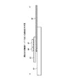
図8は、伝送路の一例を示す図である。図8に示す伝送路は、例えばマイクロストリップ型伝送線路である。このマイクロストリップ型伝送線路は、例えばポリイミドまたはガラスエポキシなどの誘電体基板21の上面に導電体により形成される信号電極22を有し、誘電体基板21の下面に導電体により形成されるグランド電極23を有していてもよい。
図10は、実施の形態にかかる光モジュールの別の例を示す図である。図11は、図10の切断線A−A'における断面を示す図である。図10及び図11に示す光モジュールは、信号電極の下の部分にグランド電極がない光モジュールの一例である。図10及び図11に示すように、光モジュールは、基板31、フォトダイオードアレイ32、信号電極33、グランド電極34及びトランスインピーダンスアンプ35を有する。
図16は、実施の形態にかかる光モジュールの別の例を示す図である。図17は、図16の切断線B−B'における断面を示す図である。図16及び図17に示す光モジュールは、フォトダイオードのカソード線が信号電極33と同じ側に引き出されている光モジュールの一例である。図16には、1つのチャネルについてのみフォトダイオードの等価回路が追記されているが、他のチャネルに対しても同様である。
図19は、実施の形態にかかる光モジュールの別の例を示す図である。図20は、図19の切断線C−C'における断面を示す図である。図21は、図20の光結合部分を拡大して示す図である。図19〜図21に示す光モジュールは、例えば図10に示す光モジュールまたは図16に示す光モジュールの実装例である。
図22は、実施の形態にかかる光モジュールの別の例を示す図である。図23は、図22の切断線D−D'における断面を示す図である。図22及び図23に示す光モジュールでは、光導波路48は、基板31の裏面においてフォトダイオードアレイ32の下から信号電極33と同じ方向へ伸び、信号電極33の下のグランド電極34のない部分36の下を通ってトランスインピーダンスアンプ35側へ至る。
Y=(1/384)×(σ×(LGAP/1000)4)/(I×E)×1000 ・・・(1)
R=I×E/(σ×(LGAP/1000)2/12) ・・・(2)
σ=1(Y<dの場合) ・・・(3)
σ=384×d×(I×E)/1000/(LGAP/1000)4) (Y>dの場合) ・・・(4)
図26は、実施の形態にかかる光モジュールの別の例を示す図である。図27は、図26の切断線E−E'における断面を示す図である。図26及び図27に示す光モジュールは、光導波路48の変形量の解析から得た知見を反映して、光導波路48の損失の劣化を抑制するようにしたものである。
図28は、実施の形態にかかる光モジュールの別の例を示す図である。図28に示す光モジュールでは、フォトダイオードアレイ32の各フォトダイオードのアノード線が信号電極33に接続され、カソード線がカソード線路39に接続され、信号電極33の下のグランド電極34のない部分36が複数に分割されている。カソード線路39は、信号電極33に沿って信号電極33から離れて設けられている。
図30は、実施の形態にかかる光モジュールの別の例を示す図である。図31は、図30の切断線F−F'における断面を示す図である。図30及び図31に示す光モジュールは、例えば図22に示す光モジュール、図26に示す光モジュールまたは図28に示す光モジュールの実装例である。
図32〜図34は、実施の形態にかかる光モジュールの製造方法の一例を示す図である。図32に示すように、例えばポリイミドなどの誘電体層の両面に銅箔が貼り付けられている基板を用意する。そして、基板の両面に対して例えばフォトリソグラフィによるレジスト転写と銅箔のエッチングによって、信号電極33やカソード線路などの伝送路のパターンと、グランド電極34のパターンとを形成する。
2 伝送路
3 増幅素子
32 フォトダイオードアレイ
33 信号電極
34 グランド電極
35,45 トランスインピーダンスアンプ
46 発光素子
47 発光素子駆動IC
48 光導波路
Claims (3)
- 光信号を受光して電気信号に変換する受光素子と、
電気信号を伝送し、誘電体層、前記誘電体層の上面に伝送路のパターンに形成された第1導電体層、及び前記誘電体層の下面に形成された第2導電体層を有し、前記第2導電体層のうち、前記受光素子と前記増幅素子とを接続する前記伝送路のパターンに対応する部分の一部または全部が空気層または誘電体層になっている伝送路と、
前記受光素子から出力されて前記伝送路により伝送されてくる電気信号を増幅する増幅素子と、
を備え、
前記受光素子と前記増幅素子とを接続する前記伝送路の特性インピーダンスが前記増幅素子の入力インピーダンスよりも高いことを特徴とする光モジュール。 - 発光素子を駆動する駆動素子と、
前記駆動素子から出力されて前記伝送路により伝送されてくる電気信号を光信号に変換する発光素子と、
を備え、
前記発光素子と前記受光素子とが並んで配置され、前記駆動素子と前記増幅素子とが、前記発光素子と前記受光素子との並びに対して反対側に配置されていることを特徴とする請求項1に記載の光モジュール。 - 前記第2導電体層の下面に、前記受光素子と光学的に結合する光導波路が、前記受光素子と前記増幅素子とを接続する前記伝送路のパターンに沿って設けられており、
前記第2導電体層のうちの前記空気層または前記誘電体層は、前記受光素子と前記増幅素子とを接続する前記伝送路のパターンに沿って複数箇所に分割して設けられていることを特徴とする請求項2に記載の光モジュール。
Priority Applications (3)
| Application Number | Priority Date | Filing Date | Title |
|---|---|---|---|
| JP2012192522A JP5983200B2 (ja) | 2012-08-31 | 2012-08-31 | 光モジュール |
| US13/900,624 US20140061441A1 (en) | 2012-08-31 | 2013-05-23 | Optical module |
| EP13170236.7A EP2713194A3 (en) | 2012-08-31 | 2013-06-03 | Optical module |
Applications Claiming Priority (1)
| Application Number | Priority Date | Filing Date | Title |
|---|---|---|---|
| JP2012192522A JP5983200B2 (ja) | 2012-08-31 | 2012-08-31 | 光モジュール |
Publications (2)
| Publication Number | Publication Date |
|---|---|
| JP2014049657A JP2014049657A (ja) | 2014-03-17 |
| JP5983200B2 true JP5983200B2 (ja) | 2016-08-31 |
Family
ID=48655950
Family Applications (1)
| Application Number | Title | Priority Date | Filing Date |
|---|---|---|---|
| JP2012192522A Expired - Fee Related JP5983200B2 (ja) | 2012-08-31 | 2012-08-31 | 光モジュール |
Country Status (3)
| Country | Link |
|---|---|
| US (1) | US20140061441A1 (ja) |
| EP (1) | EP2713194A3 (ja) |
| JP (1) | JP5983200B2 (ja) |
Families Citing this family (3)
| Publication number | Priority date | Publication date | Assignee | Title |
|---|---|---|---|---|
| JP6959731B2 (ja) * | 2016-11-30 | 2021-11-05 | 日東電工株式会社 | 光電気混載基板 |
| JP7003819B2 (ja) * | 2018-04-09 | 2022-01-21 | 富士通株式会社 | 光受信器 |
| JP7059865B2 (ja) * | 2018-08-10 | 2022-04-26 | 富士通株式会社 | 光送信器 |
Family Cites Families (26)
| Publication number | Priority date | Publication date | Assignee | Title |
|---|---|---|---|---|
| JP2952302B2 (ja) | 1989-03-13 | 1999-09-27 | 日本電信電話株式会社 | 受光素子 |
| JPH03244232A (ja) * | 1990-02-22 | 1991-10-31 | Toshiba Corp | 光受信モジュール |
| US6064507A (en) * | 1996-06-17 | 2000-05-16 | Trw Inc. | High speed differential optoelectronic receiver |
| JP3858304B2 (ja) * | 1996-06-20 | 2006-12-13 | 住友電気工業株式会社 | 光受信回路 |
| JP2001141965A (ja) | 1999-11-15 | 2001-05-25 | Canon Inc | 光結合器、その作製方法、およびこれを用いた光送受信装置、光インターコネクション装置 |
| JP3937426B2 (ja) * | 2001-07-16 | 2007-06-27 | 日本電気株式会社 | プリアンプ回路 |
| US6636414B2 (en) * | 2002-01-08 | 2003-10-21 | Raytheon Company | High power variable slide RF tuner |
| WO2003062866A2 (en) * | 2002-01-22 | 2003-07-31 | Zonu, Inc. | Flex board interface to an optical module |
| DE10215414A1 (de) * | 2002-04-08 | 2003-10-30 | Ipag Innovative Proc Ag | Lichtempfindliche Halbleiterdiodenanordnung mit passiver Anpassungsschaltung |
| JP2004095869A (ja) * | 2002-08-30 | 2004-03-25 | Mitsubishi Electric Corp | 受光素子および受光装置 |
| JP3759494B2 (ja) * | 2002-12-12 | 2006-03-22 | セイコーエプソン株式会社 | 光通信装置 |
| JP4165244B2 (ja) | 2003-02-06 | 2008-10-15 | セイコーエプソン株式会社 | 受光素子の製造方法 |
| SE0300774D0 (sv) * | 2003-03-21 | 2003-03-21 | Optillion Ab | Optical modulator |
| DE10345498B4 (de) * | 2003-09-30 | 2016-06-02 | Intel Deutschland Gmbh | Integrierte Leistungs-Verstärkeranordnung |
| US7011458B2 (en) * | 2004-07-12 | 2006-03-14 | Opnext Japan, Inc. | Optical module |
| JP4441458B2 (ja) * | 2005-08-22 | 2010-03-31 | アルプス電気株式会社 | 電子回路ユニット |
| DE102005051571B4 (de) * | 2005-10-21 | 2013-06-20 | Fraunhofer-Gesellschaft zur Förderung der angewandten Forschung e.V. | Photodioden-Chip hoher Grenzfrequenz |
| JP2007207803A (ja) * | 2006-01-31 | 2007-08-16 | Opnext Japan Inc | 光送信モジュール |
| JP2009092689A (ja) * | 2007-10-03 | 2009-04-30 | Fuji Xerox Co Ltd | 光モジュール |
| JP5118151B2 (ja) * | 2007-12-04 | 2013-01-16 | 京セミ株式会社 | 光電変換モジュール |
| CN102318143B (zh) * | 2008-12-12 | 2015-03-11 | 莫列斯公司 | 谐振调整连接器 |
| JP5378915B2 (ja) * | 2009-08-31 | 2013-12-25 | 日本オクラロ株式会社 | 光受信モジュール及び光受信器 |
| US8447187B2 (en) * | 2010-02-23 | 2013-05-21 | Vi Systems Gmbh | Optoelectronic interconnect for high frequency data transmission at low power consumption |
| JP5291144B2 (ja) * | 2011-05-17 | 2013-09-18 | 日本電信電話株式会社 | 光受信回路 |
| JP5747721B2 (ja) * | 2011-07-29 | 2015-07-15 | 富士通株式会社 | 光伝送路、光コネクタ、及び光モジュール |
| JP5840411B2 (ja) * | 2011-08-05 | 2016-01-06 | 日本メクトロン株式会社 | 光電気混載可撓性プリント配線板及びその受発光素子実装方法 |
-
2012
- 2012-08-31 JP JP2012192522A patent/JP5983200B2/ja not_active Expired - Fee Related
-
2013
- 2013-05-23 US US13/900,624 patent/US20140061441A1/en not_active Abandoned
- 2013-06-03 EP EP13170236.7A patent/EP2713194A3/en not_active Withdrawn
Also Published As
| Publication number | Publication date |
|---|---|
| JP2014049657A (ja) | 2014-03-17 |
| EP2713194A2 (en) | 2014-04-02 |
| US20140061441A1 (en) | 2014-03-06 |
| EP2713194A3 (en) | 2014-05-21 |
Similar Documents
| Publication | Publication Date | Title |
|---|---|---|
| JP6427626B2 (ja) | 誘電性導波路を用いたチップ間通信 | |
| JP5139375B2 (ja) | 光インターフェースモジュールの製造方法、及び、光インターフェースモジュール | |
| US8774576B2 (en) | Optical module and method for manufacturing the same | |
| US8989531B2 (en) | Optical-electrical wiring board and optical module | |
| JP5439080B2 (ja) | 光i/oアレイモジュール | |
| JP5580994B2 (ja) | 光モジュール | |
| US6829398B2 (en) | Optical waveguide apparatus | |
| TW200404487A (en) | A light reception/emission device built-in module with optical and electrical wiring combined therein and method of making the same | |
| WO2018198490A1 (ja) | 光電子集積回路及びコンピューティング装置 | |
| US20120224804A1 (en) | Semiconductor device and method of manufacturing the same | |
| JP2008158090A (ja) | 光配線基板 | |
| US8179620B2 (en) | Optical module | |
| JP5983200B2 (ja) | 光モジュール | |
| US11057984B2 (en) | High-speed hybrid circuit | |
| JP2007207803A (ja) | 光送信モジュール | |
| JP6084027B2 (ja) | 光導波路装置及びその製造方法 | |
| JP4656156B2 (ja) | 光通信装置 | |
| JP7300625B2 (ja) | 半導体装置の実装構造、光モジュール、及び半導体装置の実装構造の製造方法 | |
| JP2013097147A (ja) | フレキシブル光電配線モジュール | |
| JP2012195456A (ja) | フレキシブル配線モジュール及びフレキシブル配線装置 | |
| JP2016092303A (ja) | 並列光モジュール | |
| JP2013246201A (ja) | 光配線部品、光配線モジュールおよび光配線装置 | |
| JP5237171B2 (ja) | 差動配線体 | |
| JP2008122527A (ja) | 光トランシーバモジュールおよびその製造方法 | |
| JP2011227371A (ja) | 半導体パッケージ |
Legal Events
| Date | Code | Title | Description |
|---|---|---|---|
| A621 | Written request for application examination |
Free format text: JAPANESE INTERMEDIATE CODE: A621 Effective date: 20150512 |
|
| A977 | Report on retrieval |
Free format text: JAPANESE INTERMEDIATE CODE: A971007 Effective date: 20160217 |
|
| A131 | Notification of reasons for refusal |
Free format text: JAPANESE INTERMEDIATE CODE: A131 Effective date: 20160223 |
|
| A521 | Request for written amendment filed |
Free format text: JAPANESE INTERMEDIATE CODE: A523 Effective date: 20160425 |
|
| TRDD | Decision of grant or rejection written | ||
| A01 | Written decision to grant a patent or to grant a registration (utility model) |
Free format text: JAPANESE INTERMEDIATE CODE: A01 Effective date: 20160705 |
|
| A61 | First payment of annual fees (during grant procedure) |
Free format text: JAPANESE INTERMEDIATE CODE: A61 Effective date: 20160718 |
|
| R150 | Certificate of patent or registration of utility model |
Ref document number: 5983200 Country of ref document: JP Free format text: JAPANESE INTERMEDIATE CODE: R150 |
|
| LAPS | Cancellation because of no payment of annual fees |