CN101448977A - Apparatus and process for plasma-enhanced atomic layer deposition - Google Patents
Apparatus and process for plasma-enhanced atomic layer deposition Download PDFInfo
- Publication number
- CN101448977A CN101448977A CNA2006800135356A CN200680013535A CN101448977A CN 101448977 A CN101448977 A CN 101448977A CN A2006800135356 A CNA2006800135356 A CN A2006800135356A CN 200680013535 A CN200680013535 A CN 200680013535A CN 101448977 A CN101448977 A CN 101448977A
- Authority
- CN
- China
- Prior art keywords
- gas
- plasma
- assembly
- ruthenium
- chamber
- Prior art date
- Legal status (The legal status is an assumption and is not a legal conclusion. Google has not performed a legal analysis and makes no representation as to the accuracy of the status listed.)
- Granted
Links
Images


Classifications
-
- C—CHEMISTRY; METALLURGY
- C23—COATING METALLIC MATERIAL; COATING MATERIAL WITH METALLIC MATERIAL; CHEMICAL SURFACE TREATMENT; DIFFUSION TREATMENT OF METALLIC MATERIAL; COATING BY VACUUM EVAPORATION, BY SPUTTERING, BY ION IMPLANTATION OR BY CHEMICAL VAPOUR DEPOSITION, IN GENERAL; INHIBITING CORROSION OF METALLIC MATERIAL OR INCRUSTATION IN GENERAL
- C23C—COATING METALLIC MATERIAL; COATING MATERIAL WITH METALLIC MATERIAL; SURFACE TREATMENT OF METALLIC MATERIAL BY DIFFUSION INTO THE SURFACE, BY CHEMICAL CONVERSION OR SUBSTITUTION; COATING BY VACUUM EVAPORATION, BY SPUTTERING, BY ION IMPLANTATION OR BY CHEMICAL VAPOUR DEPOSITION, IN GENERAL
- C23C16/00—Chemical coating by decomposition of gaseous compounds, without leaving reaction products of surface material in the coating, i.e. chemical vapour deposition [CVD] processes
- C23C16/44—Chemical coating by decomposition of gaseous compounds, without leaving reaction products of surface material in the coating, i.e. chemical vapour deposition [CVD] processes characterised by the method of coating
- C23C16/455—Chemical coating by decomposition of gaseous compounds, without leaving reaction products of surface material in the coating, i.e. chemical vapour deposition [CVD] processes characterised by the method of coating characterised by the method used for introducing gases into reaction chamber or for modifying gas flows in reaction chamber
- C23C16/45523—Pulsed gas flow or change of composition over time
- C23C16/45525—Atomic layer deposition [ALD]
- C23C16/45544—Atomic layer deposition [ALD] characterized by the apparatus
-
- C—CHEMISTRY; METALLURGY
- C23—COATING METALLIC MATERIAL; COATING MATERIAL WITH METALLIC MATERIAL; CHEMICAL SURFACE TREATMENT; DIFFUSION TREATMENT OF METALLIC MATERIAL; COATING BY VACUUM EVAPORATION, BY SPUTTERING, BY ION IMPLANTATION OR BY CHEMICAL VAPOUR DEPOSITION, IN GENERAL; INHIBITING CORROSION OF METALLIC MATERIAL OR INCRUSTATION IN GENERAL
- C23C—COATING METALLIC MATERIAL; COATING MATERIAL WITH METALLIC MATERIAL; SURFACE TREATMENT OF METALLIC MATERIAL BY DIFFUSION INTO THE SURFACE, BY CHEMICAL CONVERSION OR SUBSTITUTION; COATING BY VACUUM EVAPORATION, BY SPUTTERING, BY ION IMPLANTATION OR BY CHEMICAL VAPOUR DEPOSITION, IN GENERAL
- C23C16/00—Chemical coating by decomposition of gaseous compounds, without leaving reaction products of surface material in the coating, i.e. chemical vapour deposition [CVD] processes
- C23C16/06—Chemical coating by decomposition of gaseous compounds, without leaving reaction products of surface material in the coating, i.e. chemical vapour deposition [CVD] processes characterised by the deposition of metallic material
- C23C16/18—Chemical coating by decomposition of gaseous compounds, without leaving reaction products of surface material in the coating, i.e. chemical vapour deposition [CVD] processes characterised by the deposition of metallic material from metallo-organic compounds
-
- C—CHEMISTRY; METALLURGY
- C23—COATING METALLIC MATERIAL; COATING MATERIAL WITH METALLIC MATERIAL; CHEMICAL SURFACE TREATMENT; DIFFUSION TREATMENT OF METALLIC MATERIAL; COATING BY VACUUM EVAPORATION, BY SPUTTERING, BY ION IMPLANTATION OR BY CHEMICAL VAPOUR DEPOSITION, IN GENERAL; INHIBITING CORROSION OF METALLIC MATERIAL OR INCRUSTATION IN GENERAL
- C23C—COATING METALLIC MATERIAL; COATING MATERIAL WITH METALLIC MATERIAL; SURFACE TREATMENT OF METALLIC MATERIAL BY DIFFUSION INTO THE SURFACE, BY CHEMICAL CONVERSION OR SUBSTITUTION; COATING BY VACUUM EVAPORATION, BY SPUTTERING, BY ION IMPLANTATION OR BY CHEMICAL VAPOUR DEPOSITION, IN GENERAL
- C23C16/00—Chemical coating by decomposition of gaseous compounds, without leaving reaction products of surface material in the coating, i.e. chemical vapour deposition [CVD] processes
- C23C16/44—Chemical coating by decomposition of gaseous compounds, without leaving reaction products of surface material in the coating, i.e. chemical vapour deposition [CVD] processes characterised by the method of coating
- C23C16/455—Chemical coating by decomposition of gaseous compounds, without leaving reaction products of surface material in the coating, i.e. chemical vapour deposition [CVD] processes characterised by the method of coating characterised by the method used for introducing gases into reaction chamber or for modifying gas flows in reaction chamber
- C23C16/45523—Pulsed gas flow or change of composition over time
- C23C16/45525—Atomic layer deposition [ALD]
- C23C16/45527—Atomic layer deposition [ALD] characterized by the ALD cycle, e.g. different flows or temperatures during half-reactions, unusual pulsing sequence, use of precursor mixtures or auxiliary reactants or activations
- C23C16/45536—Use of plasma, radiation or electromagnetic fields
- C23C16/45542—Plasma being used non-continuously during the ALD reactions
-
- C—CHEMISTRY; METALLURGY
- C23—COATING METALLIC MATERIAL; COATING MATERIAL WITH METALLIC MATERIAL; CHEMICAL SURFACE TREATMENT; DIFFUSION TREATMENT OF METALLIC MATERIAL; COATING BY VACUUM EVAPORATION, BY SPUTTERING, BY ION IMPLANTATION OR BY CHEMICAL VAPOUR DEPOSITION, IN GENERAL; INHIBITING CORROSION OF METALLIC MATERIAL OR INCRUSTATION IN GENERAL
- C23C—COATING METALLIC MATERIAL; COATING MATERIAL WITH METALLIC MATERIAL; SURFACE TREATMENT OF METALLIC MATERIAL BY DIFFUSION INTO THE SURFACE, BY CHEMICAL CONVERSION OR SUBSTITUTION; COATING BY VACUUM EVAPORATION, BY SPUTTERING, BY ION IMPLANTATION OR BY CHEMICAL VAPOUR DEPOSITION, IN GENERAL
- C23C16/00—Chemical coating by decomposition of gaseous compounds, without leaving reaction products of surface material in the coating, i.e. chemical vapour deposition [CVD] processes
- C23C16/44—Chemical coating by decomposition of gaseous compounds, without leaving reaction products of surface material in the coating, i.e. chemical vapour deposition [CVD] processes characterised by the method of coating
- C23C16/455—Chemical coating by decomposition of gaseous compounds, without leaving reaction products of surface material in the coating, i.e. chemical vapour deposition [CVD] processes characterised by the method of coating characterised by the method used for introducing gases into reaction chamber or for modifying gas flows in reaction chamber
- C23C16/45523—Pulsed gas flow or change of composition over time
- C23C16/45525—Atomic layer deposition [ALD]
- C23C16/45553—Atomic layer deposition [ALD] characterized by the use of precursors specially adapted for ALD
-
- C—CHEMISTRY; METALLURGY
- C23—COATING METALLIC MATERIAL; COATING MATERIAL WITH METALLIC MATERIAL; CHEMICAL SURFACE TREATMENT; DIFFUSION TREATMENT OF METALLIC MATERIAL; COATING BY VACUUM EVAPORATION, BY SPUTTERING, BY ION IMPLANTATION OR BY CHEMICAL VAPOUR DEPOSITION, IN GENERAL; INHIBITING CORROSION OF METALLIC MATERIAL OR INCRUSTATION IN GENERAL
- C23C—COATING METALLIC MATERIAL; COATING MATERIAL WITH METALLIC MATERIAL; SURFACE TREATMENT OF METALLIC MATERIAL BY DIFFUSION INTO THE SURFACE, BY CHEMICAL CONVERSION OR SUBSTITUTION; COATING BY VACUUM EVAPORATION, BY SPUTTERING, BY ION IMPLANTATION OR BY CHEMICAL VAPOUR DEPOSITION, IN GENERAL
- C23C16/00—Chemical coating by decomposition of gaseous compounds, without leaving reaction products of surface material in the coating, i.e. chemical vapour deposition [CVD] processes
- C23C16/44—Chemical coating by decomposition of gaseous compounds, without leaving reaction products of surface material in the coating, i.e. chemical vapour deposition [CVD] processes characterised by the method of coating
- C23C16/455—Chemical coating by decomposition of gaseous compounds, without leaving reaction products of surface material in the coating, i.e. chemical vapour deposition [CVD] processes characterised by the method of coating characterised by the method used for introducing gases into reaction chamber or for modifying gas flows in reaction chamber
- C23C16/45563—Gas nozzles
- C23C16/45565—Shower nozzles
-
- C—CHEMISTRY; METALLURGY
- C23—COATING METALLIC MATERIAL; COATING MATERIAL WITH METALLIC MATERIAL; CHEMICAL SURFACE TREATMENT; DIFFUSION TREATMENT OF METALLIC MATERIAL; COATING BY VACUUM EVAPORATION, BY SPUTTERING, BY ION IMPLANTATION OR BY CHEMICAL VAPOUR DEPOSITION, IN GENERAL; INHIBITING CORROSION OF METALLIC MATERIAL OR INCRUSTATION IN GENERAL
- C23C—COATING METALLIC MATERIAL; COATING MATERIAL WITH METALLIC MATERIAL; SURFACE TREATMENT OF METALLIC MATERIAL BY DIFFUSION INTO THE SURFACE, BY CHEMICAL CONVERSION OR SUBSTITUTION; COATING BY VACUUM EVAPORATION, BY SPUTTERING, BY ION IMPLANTATION OR BY CHEMICAL VAPOUR DEPOSITION, IN GENERAL
- C23C16/00—Chemical coating by decomposition of gaseous compounds, without leaving reaction products of surface material in the coating, i.e. chemical vapour deposition [CVD] processes
- C23C16/44—Chemical coating by decomposition of gaseous compounds, without leaving reaction products of surface material in the coating, i.e. chemical vapour deposition [CVD] processes characterised by the method of coating
- C23C16/50—Chemical coating by decomposition of gaseous compounds, without leaving reaction products of surface material in the coating, i.e. chemical vapour deposition [CVD] processes characterised by the method of coating using electric discharges
- C23C16/505—Chemical coating by decomposition of gaseous compounds, without leaving reaction products of surface material in the coating, i.e. chemical vapour deposition [CVD] processes characterised by the method of coating using electric discharges using radio frequency discharges
- C23C16/509—Chemical coating by decomposition of gaseous compounds, without leaving reaction products of surface material in the coating, i.e. chemical vapour deposition [CVD] processes characterised by the method of coating using electric discharges using radio frequency discharges using internal electrodes
- C23C16/5096—Flat-bed apparatus
-
- H—ELECTRICITY
- H01—ELECTRIC ELEMENTS
- H01J—ELECTRIC DISCHARGE TUBES OR DISCHARGE LAMPS
- H01J37/00—Discharge tubes with provision for introducing objects or material to be exposed to the discharge, e.g. for the purpose of examination or processing thereof
- H01J37/32—Gas-filled discharge tubes
- H01J37/32009—Arrangements for generation of plasma specially adapted for examination or treatment of objects, e.g. plasma sources
- H01J37/32082—Radio frequency generated discharge
-
- H—ELECTRICITY
- H01—ELECTRIC ELEMENTS
- H01J—ELECTRIC DISCHARGE TUBES OR DISCHARGE LAMPS
- H01J37/00—Discharge tubes with provision for introducing objects or material to be exposed to the discharge, e.g. for the purpose of examination or processing thereof
- H01J37/32—Gas-filled discharge tubes
- H01J37/32431—Constructional details of the reactor
- H01J37/3244—Gas supply means
- H01J37/32449—Gas control, e.g. control of the gas flow
-
- H—ELECTRICITY
- H01—ELECTRIC ELEMENTS
- H01J—ELECTRIC DISCHARGE TUBES OR DISCHARGE LAMPS
- H01J37/00—Discharge tubes with provision for introducing objects or material to be exposed to the discharge, e.g. for the purpose of examination or processing thereof
- H01J37/32—Gas-filled discharge tubes
- H01J37/32431—Constructional details of the reactor
- H01J37/32458—Vessel
- H01J37/32522—Temperature
-
- H—ELECTRICITY
- H01—ELECTRIC ELEMENTS
- H01J—ELECTRIC DISCHARGE TUBES OR DISCHARGE LAMPS
- H01J37/00—Discharge tubes with provision for introducing objects or material to be exposed to the discharge, e.g. for the purpose of examination or processing thereof
- H01J37/32—Gas-filled discharge tubes
- H01J37/32431—Constructional details of the reactor
- H01J37/32623—Mechanical discharge control means
- H01J37/32633—Baffles
-
- H10P14/432—
-
- H10W20/035—
-
- H10W20/043—
-
- H10W20/034—
-
- H10W20/0425—
Landscapes
- Chemical & Material Sciences (AREA)
- Engineering & Computer Science (AREA)
- Physics & Mathematics (AREA)
- Plasma & Fusion (AREA)
- General Chemical & Material Sciences (AREA)
- Chemical Kinetics & Catalysis (AREA)
- Materials Engineering (AREA)
- Mechanical Engineering (AREA)
- Metallurgy (AREA)
- Organic Chemistry (AREA)
- Analytical Chemistry (AREA)
- Electromagnetism (AREA)
- Chemical Vapour Deposition (AREA)
- Condensed Matter Physics & Semiconductors (AREA)
- General Physics & Mathematics (AREA)
- Manufacturing & Machinery (AREA)
- Computer Hardware Design (AREA)
- Microelectronics & Electronic Packaging (AREA)
- Power Engineering (AREA)
- Plasma Technology (AREA)
Abstract
Description
技术领域 technical field
本发明的实施例是涉及一种用于沉积材料的设备与工艺。更具体地说,是涉及一种在等离子体增强的工艺中沉积材料的原子层沉积腔体。Embodiments of the invention relate to an apparatus and process for depositing materials. More specifically, it relates to an atomic layer deposition chamber for depositing materials in a plasma-enhanced process.
背景技术 Background technique
在半导体工艺、平面显示器工艺或其它电子装置工艺的领域中,气相沉积方法对于沉积材料于基材上扮演着重要角色。随着电子装置的几何形状持续缩小与组件密度持续增加,特征的尺寸与深宽比变的更具挑战性,例如特征尺寸为0.07微米(μm)与深宽比为10或更大。因此,形成这些装置的材料的共形沉积变的日益重要。In the field of semiconductor technology, flat panel display technology or other electronic device technology, vapor deposition methods play an important role in depositing materials on substrates. As the geometries of electronic devices continue to shrink and device densities continue to increase, feature sizes and aspect ratios become more challenging, such as feature sizes of 0.07 microns (μm) and aspect ratios of 10 or greater. Therefore, conformal deposition of materials forming these devices is becoming increasingly important.
公知的化学气相沉积工艺(CVD)可有效地使装置的几何形状与深宽比降至0.15微米规格,然而更精进的装置几何形状则需要其它沉积技术。其中一颇受注意的沉积技术为原子层沉积工艺(atomic layer deposition,ALD)。在原子层沉积工艺中,是相继地导入反应物气体至具有基材的工艺腔体中。通常,第一反应物是以脉冲方式注入工艺腔体中且被吸附至基材表面上。第二反应物以脉冲方式注入工艺腔体中并与第一反应物发生反应而形成一沉积材料。在每种反应气体的输送步骤之间通常会执行清洗(purge)步骤。清洗步骤可为利用载气做连续清洗的步骤或是在反应气体输送之间做脉冲清洗的步骤。热诱导原子层沉积工艺(thermally induced ALD process)是最常见的原子层沉积技术,且该技术使用热量来引发两种反应物之间的化学反应。热原子层沉积工艺虽可良好的沉积某些材料,但是通常有较慢的沉积速率。因此,会造成无法接受的制造产率。较高沉积温度可增加沉积速率,但是许多化学前驱物(precursor),特别是金属有机化合物,会在高温时分解。Known chemical vapor deposition processes (CVD) are effective for device geometries and aspect ratios down to the 0.15 micron scale, however more sophisticated device geometries require other deposition techniques. One of the deposition techniques that has attracted much attention is atomic layer deposition (ALD). In the atomic layer deposition process, reactant gases are sequentially introduced into the process chamber with the substrate. Typically, the first reactant is pulsed into the process chamber and adsorbed onto the surface of the substrate. The second reactant is pulsed into the process chamber and reacts with the first reactant to form a deposition material. A purge step is usually performed between the delivery steps of each reactant gas. The cleaning step can be a continuous cleaning step using a carrier gas or a pulse cleaning step between reactant gas delivery. The thermally induced ALD process is the most common ALD technique and uses heat to initiate a chemical reaction between two reactants. Thermal ALD processes deposit some materials well, but generally have slower deposition rates. Consequently, unacceptable manufacturing yields can result. Higher deposition temperatures increase deposition rates, but many chemical precursors, especially metal organic compounds, decompose at high temperatures.
等离子体增强的原子层沉积工艺(PE-ALD)为另一种公知的材料形成技术。在一些PE-ALD工艺范例中,可利用热原子层沉积工艺所使用的相同化学前驱物来形成材料,但是却可具有较高沉积速率与较低温度。虽然存在各种技术,一般而言,PE-ALD工艺提供连续导入反应气体与反应物等离子体至具有基材的工艺腔体中。第一反应物气体是以脉冲方式注入工艺腔体中且被吸附至基材表面上。之后,第二反应物等离子体是以脉冲方式注入工艺腔体中并与第一反应物气体反应而形成沉积材料。与热ALD工艺类似的是,在每个反应物的输送步骤之间可进行清洗步骤。虽然由于反应物自由基在等离子体中的高反应性使PE-ALD工艺可克服某些热ALD工艺的缺点,但PE-ALD工艺同时也具有诸多限制。PE-ALD工艺可能造成等离子体对基材的损害(例如,侵蚀),而与某些化学前驱物不兼容并且需要额外的硬件。Plasma enhanced atomic layer deposition (PE-ALD) is another well known material formation technique. In some PE-ALD process examples, materials can be formed using the same chemical precursors used in thermal ALD processes, but at higher deposition rates and lower temperatures. Although various techniques exist, in general, the PE-ALD process provides continuous introduction of reactant gas and reactant plasma into a process chamber with a substrate. The first reactant gas is injected into the process chamber in a pulsed manner and is adsorbed on the surface of the substrate. Afterwards, the second reactant plasma is pulsed into the process chamber and reacts with the first reactant gas to form a deposition material. Similar to the thermal ALD process, a purge step may be performed between each reactant delivery step. Although the PE-ALD process can overcome some of the disadvantages of the thermal ALD process due to the high reactivity of the reactant radicals in the plasma, the PE-ALD process also has many limitations. The PE-ALD process can cause plasma damage to the substrate (eg, erosion), is incompatible with certain chemical precursors, and requires additional hardware.
因此,对于利用气相沉积技术,较佳地为等离子体增强的技术,更佳为等离子体增强的原子层沉积技术来沉积或形成材料于基材上的设备与工艺存在着需求。Therefore, there is a need for equipment and processes for depositing or forming materials on substrates using vapor deposition techniques, preferably plasma-enhanced techniques, more preferably plasma-enhanced atomic layer deposition techniques.
发明内容 Contents of the invention
本发明的实施例提供一种可在诸如等离子体增强的原子层沉积(PE-ALD)之类的原子层沉积工艺中形成材料的设备。在一实施例中,工艺腔体是用以使基材于PE-ALD工艺中接触一连串的气体与等离子体。工艺腔体包含多个电性绝缘、电性接地或射频激化的零件。在一个范例中,腔体主体与气体歧管(manifold)组件是接地且通过例如绝缘套、等离子体筛插件与隔离环等电性绝缘零件加以分隔开。一喷头、一等离子体隔板与一水盒是设置在这些绝缘零件之间,并且在喷头、等离子体隔板与水盒受到等离子体产生器启动时会变成具有射频热(RF hot)。Embodiments of the present invention provide an apparatus that can form materials in an atomic layer deposition process such as plasma enhanced atomic layer deposition (PE-ALD). In one embodiment, the process chamber is used to expose the substrate to a series of gas and plasma in the PE-ALD process. Process chambers contain multiple electrically isolated, electrically grounded, or RF energized parts. In one example, the chamber body and the gas manifold assembly are grounded and separated by electrically insulating components such as insulating sleeves, plasma screen inserts, and isolation rings. A shower head, a plasma partition and a water box are disposed between the insulating parts, and become RF hot when the shower head, the plasma partition and the water box are activated by the plasma generator.
在一范例中,提供一种处理基材的腔体,其包含一基材支持件与一腔体盖组件,该支持件包含基材接收表面,而且基材支持件与腔体盖组件之间具有一工艺区域。在一实施例中,腔体盖组件包含具有一内部区域与外部区域的一喷头组件、与该喷头组件接触之一冷却组件、设置在该喷头组件内部区域中的一等离子体隔板、位于该喷头组件上方且用以引导第一工艺气体至该等离子体隔板与引导第二工艺气体至该喷头组件外部区域的一等离子体筛、一位于该等离子体隔板与该等离子体筛之间的第一气体区域、以及位于该喷头外部区域与该冷却组件之间的第二气体区域。In one example, a chamber for processing a substrate is provided, which includes a substrate support and a chamber lid assembly, the support includes a substrate receiving surface, and the substrate support and the chamber lid assembly There is a process area. In one embodiment, the chamber cover assembly includes a showerhead assembly having an interior region and an exterior region, a cooling assembly in contact with the showerhead assembly, a plasma baffle disposed in the interior region of the showerhead assembly, a plasma screen above the showerhead assembly for directing the first process gas to the plasma baffle and the second process gas to the outer area of the showerhead assembly, and a plasma screen between the plasma baffle and the plasma screen A first gas zone, and a second gas zone between the showerhead outer zone and the cooling assembly.
在另一范例中,提供处理基材的一腔体,其包含一基材支持件与一腔体盖组件,该基材支持件包含一基材接收表面,该腔体盖组件包含一信道,该信道位于该腔体盖组件的中央部位。一端较窄的底表面(tapered bottomsurface)是从该通道延伸至等离子体筛处并且位于一等离子体隔板与一喷头的上方,其中该喷头的尺寸与形状可加以调整以实质涵盖该基材接收表面,一第一导管连接至该通道内的第一气体入口以及一第二导管连接至该通道内第二气体入口,其中该第一导管与第二导管是用以提供环形方向的气体流。In another example, a chamber for processing substrates is provided comprising a substrate support and a chamber cover assembly, the substrate support comprising a substrate receiving surface, the chamber cover assembly comprising a channel, The channel is located in the central portion of the cavity cover assembly. A tapered bottom surface extending from the channel to the plasma screen over a plasma baffle and a showerhead sized and shaped to substantially encompass the substrate receiving surface. On the surface, a first conduit is connected to the first gas inlet in the channel and a second conduit is connected to the second gas inlet in the channel, wherein the first conduit and the second conduit are used to provide gas flow in an annular direction.
在另一实施例中,提供一种用以处理基材的腔体,其包含具有一基材接收表面的一基材支持件、具有一含内部区域与外部区域的喷头组件的腔体盖组件、位于该喷头组件上方且用以引导第一工艺气体至该内部区域与引导第二工艺气体至该外部区域的一等离子体筛、以及一位于该基材接收表面与该腔体盖组件之间的工艺区域。等离子体筛包含用以接收该第一工艺气体的一内面积(inner area)以及用以接收该第二工艺气体的一外面积。In another embodiment, a chamber for processing a substrate is provided that includes a substrate support having a substrate receiving surface, a chamber cover assembly having a showerhead assembly including an inner region and an outer region. , a plasma screen positioned above the showerhead assembly for directing a first process gas to the inner region and a second process gas to the outer region, and a plasma screen positioned between the substrate receiving surface and the chamber lid assembly process area. The plasma screen includes an inner area for receiving the first process gas and an outer area for receiving the second process gas.
在另一实施例中,盖组件是用以使基材于PE-ALD工艺中接触一连串的气体与等离子体。盖组件包含多个电性绝缘、电性接地或RF激化的组件。在一范例中,盖组件包含一接地的气体歧管组件,其位于例如绝缘套、等离子体筛插件与隔离环等电性绝缘零件的上方。一喷头、一等离子体隔板与一水盒(water box)是设置在绝缘零件之间,且在受到等离子体产生器启动时,喷头、等离子体隔板与水盒会变得射频热(RF hot)。In another embodiment, a lid assembly is used to expose a substrate to a series of gases and plasmas in a PE-ALD process. The cover assembly contains a plurality of electrically isolated, electrically grounded or RF energized components. In one example, the cover assembly includes a grounded gas manifold assembly positioned above electrically insulating components such as insulating sleeves, plasma screen inserts, and spacer rings. A shower head, a plasma partition and a water box (water box) are arranged between the insulating parts, and when activated by the plasma generator, the shower head, the plasma partition and the water box will become radio frequency heat (RF hot).
在一范例中,喷头组件包含一喷头面板,其具有一下表面以实质涵盖该基材接收表面。该喷头组件的内部区域包含一可移除式的等离子体隔板。该喷头组件与等离子体隔板通常包含导电材料,例如铝、不锈钢、钢、铁、铬、镍、上述金属的合金或组合物等。再者,该喷头面板的下表面与该等离子体隔板是与该基材接收表面平行或实质平行设置,且连接至一电源以激发等离子体。该喷头组件的外部区域包含多个与工艺区域流体连通的孔。每个孔的直径介于约0.2毫米(mm)至约0.8毫米之间,较佳地,是介于约0.4毫米至约0.6毫米之间,诸如0.51毫米。喷头面板可包含大约1000个或更多个孔,例如大约1500个或更多个孔。这些孔具有可抑制气体往回扩散或抑制次级等离子体(secondary plasma)形成的直径。In one example, the showerhead assembly includes a showerhead plate having a lower surface substantially encompassing the substrate receiving surface. The interior region of the showerhead assembly includes a removable plasma baffle. The showerhead assembly and plasma baffle typically comprise conductive materials such as aluminum, stainless steel, steel, iron, chromium, nickel, alloys or combinations thereof, and the like. Furthermore, the lower surface of the showerhead panel and the plasma partition are arranged parallel or substantially parallel to the substrate receiving surface, and are connected to a power source to activate plasma. The outer region of the showerhead assembly contains a plurality of holes in fluid communication with the process region. The diameter of each hole is between about 0.2 millimeter (mm) and about 0.8 mm, preferably between about 0.4 mm and about 0.6 mm, such as 0.51 mm. The showerhead panel may contain about 1000 or more holes, such as about 1500 or more holes. These holes have a diameter that inhibits the back diffusion of gas or the formation of secondary plasma.
在另一个实施例中,提供一个用以在工艺腔体中执行气相沉积工艺的盖组件,其包含一绝缘套(insulation cap)与一等离子体筛(plasma screen),其中该绝缘套包括用以导流第一工艺气体的第一通道,以及该等离子体筛具有一上表面,该上表面具有一内面积与一外面积。该绝缘套可位于该等离子体筛的上表面上。等离子体筛的内面积内的多个第一开口是用以将来自上表面的第一工艺气体引导到一下表面下方,以及在等离子体筛的外面积内的多个第二开口是用以将来自该上表面上方的第二工艺气体引导到该下表面下方。在一个范例中,该多个第一开口可以是多个孔,以及该多个第二开口可以是多个狭缝(slots)。再者,绝缘套可包含一第二通道,其用以导流该第二工艺气体至该等离子体筛的外面积处。该等离子体筛的该内面积包含一无孔区带,以及该第一工艺气体的第一流动型态(flow pattern)是以视距方向(line-of-sight)朝向该无孔区带。第一流动型态的视距方向会阻碍该多个孔,以避免在等离子体筛的上表面上方激发出次级等离子体。在一个范例中,每个孔的直径介于约0.5毫米至约5毫米之间,较佳地,是介于约1毫米至约3毫米之间,更佳地是约1.5毫米。该多个孔可包含至少约100个孔,较佳地至少约150个孔。绝缘套与等离子体筛可各自由一电性绝缘、绝热或电与热同时绝缘的材料所形成,例如陶瓷材料、石英材料或上述材料的衍生物。In another embodiment, a cap assembly for performing a vapor deposition process in a process chamber is provided, which includes an insulation cap and a plasma screen, wherein the insulation cap includes an insulation cap for The first channel guiding the first process gas, and the plasma screen has an upper surface, and the upper surface has an inner area and an outer area. The insulating sleeve may be located on the upper surface of the plasma screen. A plurality of first openings in the inner area of the plasma screen to direct the first process gas from the upper surface below the lower surface, and a plurality of second openings in the outer area of the plasma screen to direct A second process gas from above the upper surface is directed below the lower surface. In one example, the plurality of first openings may be a plurality of holes, and the plurality of second openings may be a plurality of slots. Furthermore, the insulating casing may include a second channel for guiding the second process gas to the outer surface of the plasma screen. The inner area of the plasma screen includes a non-porous zone, and a first flow pattern of the first process gas is line-of-sight toward the non-porous zone. The line-of-sight direction of the first flow regime obstructs the plurality of holes to avoid excitation of secondary plasma above the upper surface of the plasma screen. In one example, the diameter of each hole is between about 0.5 mm and about 5 mm, preferably between about 1 mm and about 3 mm, more preferably about 1.5 mm. The plurality of pores may comprise at least about 100 pores, preferably at least about 150 pores. The insulating sleeve and the plasma screen can each be formed of an electrically insulating, thermally insulating or both electrically and thermally insulating material, such as a ceramic material, a quartz material, or a derivative thereof.
在另一个实施例中,喷头组件包含一喷头与一等离子体隔板,用以于等离子体增强的气相沉积腔体中分散工艺气体。喷头面板包含一内面积与一外面积,该内面积是用以将该等离子体隔板设置于其中,以及该外面积具有多个用以释出工艺气体的孔。等离子体隔板包含一用以接收其它工艺气体且位于一上表面上的头锥(nose)、用以释出工艺气体的一下表面、以及用以将工艺气体由该上表面导流至工艺区域的多个开口。这些开口较佳地为狭缝(slot),并以一预定角度设置成一环形流动型态用以释出工艺气体。In another embodiment, a showerhead assembly includes a showerhead and a plasma baffle for dispersing process gases in a plasma enhanced vapor deposition chamber. The showerhead panel includes an inner area for disposing the plasma baffle therein and an outer area having a plurality of holes for releasing process gas. The plasma baffle includes a nose on an upper surface for receiving other process gases, a lower surface for releasing process gases, and a nose for guiding process gases from the upper surface to the process area multiple openings. These openings are preferably slots and are arranged at a predetermined angle in an annular flow pattern for releasing the process gas.
在一范例中,等离子体隔板组件包含多个狭缝,其由第一气体区域延伸通过该等离子体隔板组件以提供第一气体区域流体连通至工艺区域。等离子体隔板组件更包含一头锥,其由等离子体隔板的上表面延伸至等离子体筛的下表面。这些狭缝由中央部位以正切角度延伸横越介于头锥与等离子体隔板组件外缘的该上表面。每个狭缝是相对基材接收表面以一预设喷射角(injection angle)延伸穿过等离子体隔板组件。此预设喷射角可介于约20°至约70°之间,较佳地是介于约30°至60°之间,更佳地介于约40°至50°之间,例如约45°。每个狭缝的宽度是介于约0.6毫米至约0.9毫米之间,较佳地介于约0.7毫米至0.8毫米之间,例如约0.76毫米;以及其长度介于约10毫米至约50毫米之间,较佳地介于约20毫米至约30毫米之间,例如约23毫米或更长。等离子体隔板组件通常包含约10个或更多的狭缝,例如约20个或更多的狭缝。狭缝具有可抑制气体往回扩散或次级等离子体形成的宽度。在一个范例中,等离子体隔板的上表面是由头锥处向下延伸。上表面可具有角度以接收通过狭缝开口的工艺气体,并以均匀的流速分散该工艺气体。In one example, the plasma baffle assembly includes a plurality of slots extending from the first gas region through the plasma baffle assembly to provide fluid communication of the first gas region to the process region. The plasma baffle assembly further includes a nose cone extending from the upper surface of the plasma baffle to the lower surface of the plasma screen. The slots extend from a central portion at a tangential angle across the upper surface between the nose cone and the outer edge of the plasma baffle assembly. Each slot extends through the plasma baffle assembly at a predetermined injection angle relative to the substrate receiving surface. This preset spray angle can be between about 20° to about 70°, preferably between about 30° to 60°, more preferably between about 40° to 50°, for example about 45° °. The width of each slit is between about 0.6mm and about 0.9mm, preferably between about 0.7mm and 0.8mm, such as about 0.76mm; and its length is between about 10mm and about 50mm Between, preferably between about 20 mm to about 30 mm, such as about 23 mm or longer. Plasma baffle assemblies typically contain about 10 or more slots, such as about 20 or more slots. The slit has a width that inhibits gas back diffusion or secondary plasma formation. In one example, the upper surface of the plasma baffle extends downward from the nose cone. The upper surface may be angled to receive process gas passing through the slot opening and disperse the process gas at a uniform flow rate.
在另一个实施例中,提供一种在等离子体增强的气相沉积腔体中用于接收工艺气体的等离子体隔板组件,其包含一等离子体隔板面板,该等离子体隔板面板具有一接收工艺气体的上表面以及一用以释出工艺气体的下表面。等离子体隔板组件包含多个开口,用以将来自上表面上方的工艺气体导流到下表面下方,其中每个开口是以一阻碍角度(obscured angle)或预设角度设置,该角度是由下表面的垂直轴处测量。In another embodiment, a plasma baffle assembly for receiving a process gas in a plasma enhanced vapor deposition chamber is provided that includes a plasma baffle panel having a receiving An upper surface for process gas and a lower surface for releasing process gas. The plasma baffle assembly includes a plurality of openings for guiding process gas from above the upper surface to below the lower surface, wherein each opening is arranged at an obstructed angle or a predetermined angle, which is defined by Measured at the vertical axis of the lower surface.
在另一个实施例中,冷却组件包含多个通路(passageway),以使第二工艺气体通往第二气体区域。多个通路使该等离子体筛与第二气体区域之间流体连通。多个通路包含至少约10个通道,较佳地包含至少约20个通道,以及更佳地包含至少约30个通道,例如约36个通道。In another embodiment, the cooling assembly includes a plurality of passageways for passing the second process gas to the second gas region. A plurality of passages provide fluid communication between the plasma screen and the second gas zone. The plurality of pathways comprises at least about 10 channels, preferably at least about 20 channels, and more preferably at least about 30 channels, such as about 36 channels.
在另一个范例中,提供一种用以进行气相沉积工艺的喷头组件,其包含一喷头面板;并且该喷头面板具有一可在工艺腔体中实质涵盖基材接收表面的底表面、一用以输配第一工艺气体通过相对基材接收表面具有预设喷射角的多个狭缝的内部区域、以及一用以输配第二工艺气体通过有多个孔的外部区域。In another example, a showerhead assembly for performing a vapor deposition process is provided, which includes a showerhead panel; and the showerhead panel has a bottom surface substantially covering a substrate receiving surface in a process chamber, a The first process gas is delivered through an inner area of a plurality of slits having predetermined injection angles relative to the receiving surface of the substrate, and an outer area is used for delivering a second process gas through a plurality of holes.
在另一个实施例中,提供一种在等离子体增强的气相沉积腔体中用于接收工艺气体的喷头组件,其包含一喷头面板,该喷头面板具有一用以接收气体的上表面以及一用以释出气体的下表面。用于接收第一工艺气体的上表面的一内面积包含多个第一开口,用以将上表面上方的第一工艺气体引导至下表面的下方。用于接收第二工艺气体的上表面的一外面积包含多个第二开口,用以将上表面上方的第二工艺气体导流至下表面的下方。例如,冷却组件可位于喷头面板上方且与其接触。一内部区域形成在该内面积与冷却组件之间,而一外部区域形成在该外面积与冷却组件之间。喷头面板的内部区域可包含一等离子体隔板。In another embodiment, a showerhead assembly for receiving a process gas in a plasma-enhanced vapor deposition chamber is provided, which includes a showerhead panel having an upper surface for receiving a gas and a to release gas from the lower surface. An inner area of the upper surface for receiving the first process gas includes a plurality of first openings for guiding the first process gas above the upper surface to below the lower surface. An outer area of the upper surface for receiving the second process gas includes a plurality of second openings for guiding the second process gas above the upper surface to below the lower surface. For example, a cooling assembly may be positioned above and in contact with the showerhead panel. An inner region is formed between the inner area and the cooling element, and an outer region is formed between the outer area and the cooling element. The interior region of the showerhead panel may contain a plasma baffle.
在另一个范例中,冷却组件包含多个通路,用以引导第二工艺气体进入该外部区域中。每个通路是以一预设角度延伸至外部区域。该预设角度可抑制气体往回扩散或次级等离子体的形成。在一个范例中,此预设喷射角可介于约5°至约85°之间,较佳地是介于约10°至45°之间,更佳地介于约15°至35°之间。每个通路为第二工艺气体提供进入外部区域的隐匿流动路径(obscured flow path)。在范例中,冷却组件可具有约36个通路。In another example, the cooling assembly includes a plurality of passages for directing the second process gas into the outer region. Each passage extends to the outer area at a predetermined angle. The predetermined angle can inhibit the back diffusion of gas or the formation of secondary plasma. In one example, the preset spray angle may be between about 5° and about 85°, preferably between about 10° and 45°, more preferably between about 15° and 35° between. Each passage provides an obscured flow path for the second process gas into the outer region. In an example, a cooling assembly may have approximately 36 passages.
在另一个实施例中,提供用以在工艺腔体中进行气相沉积工艺的盖组件,其包含一绝缘套与一等离子体筛。在范例中,绝缘套具有一中央信道与一外信道,该中央信道用以将来自上表面的第一工艺气体引导至一扩充通道处(expanded channel);以及该外通道是用以将来自上表面的第二工艺气体引导至一凹槽(groove)处,该凹槽包围着该扩充通道。在范例中,等离子体筛具有一上表面,该上表面包含一具有多个孔的内面积与一具有多个狭缝的外面积。绝缘套可位于等离子体筛的顶端,以形成一具有扩充信道的中央气体区域以及一具有凹槽的环形气体区域。In another embodiment, a lid assembly for performing a vapor deposition process in a process chamber is provided, which includes an insulating sleeve and a plasma screen. In an example, the insulating sleeve has a central channel and an outer channel, the central channel is used to guide the first process gas from the upper surface to an expanded channel (expanded channel); and the outer channel is used to guide the first process gas from the upper surface The second process gas at the surface is directed to a groove surrounding the extended channel. In an example, the plasma screen has an upper surface including an inner area with a plurality of holes and an outer area with a plurality of slits. An insulating sleeve may be positioned on top of the plasma screen to form a central gas zone with expanded channels and an annular gas zone with grooves.
在另一个范例中,绝缘套位于等离子体筛的上方。绝缘套包含至少二个气体通路,使得一第一气体通路用以引导第一工艺气体进入等离子体筛的内部区域中,以及一第二气体通路用以引导第二工艺气体进入等离子体筛的外部区域中。绝缘套包含电性绝缘材料,例如陶瓷材料、石英材料或上述材料的衍生物。In another example, the insulating jacket is located above the plasma screen. The insulating casing comprises at least two gas passages, such that a first gas passage is used to guide a first process gas into the inner region of the plasma screen, and a second gas passage is used to guide a second process gas into the exterior of the plasma screen. in the area. The insulating sleeve comprises an electrically insulating material, such as ceramic material, quartz material or derivatives of the above materials.
在另一个范例中,气体歧管是设置在绝缘套上方且包含至少二个气体通路。设置一第一气体通路以提供第一工艺气体通至绝缘套处,以及设置一第二气体通路以提供第二工艺气体通至绝缘套处。一第一导管与一第二导管可连接至该第一气体通路并为该第一工艺气体提供环形方向的气流方式。第一与第二导管是独立设置以引导在第一气体通路内表面处的气体。气体流通常具有环形方向,其几何形状可为漩涡状(vortex)、螺纹状(helix)、螺旋状(spiral)、旋转状(twirl)、扭转状(twist)、盘绕状(coil)、圈状(whirlpool)或上述形状的衍生形状。第一与第二导管是各自与第一气体通路的中央轴间具有一角度。此角度可大于0°,较佳地大于约20°,更佳地大于约35°。一阀(valve)可连接在该第一导管与一前驱物源之间,以使ALD工艺具有大约10秒或更短的脉冲时间,较佳地是大约6秒或更短,更佳地是大约1秒或更短,例如介于约0.01秒至约0.5秒之间。In another example, the gas manifold is disposed above the insulating casing and includes at least two gas passages. A first gas channel is provided to provide the first process gas to pass to the insulating sleeve, and a second gas channel is provided to provide the second process gas to pass to the insulating sleeve. A first conduit and a second conduit may be connected to the first gas passage and provide the first process gas with an annular direction of flow. The first and second conduits are independently disposed to guide gas at the inner surface of the first gas passage. The gas flow usually has a circular orientation and its geometry can be vortex, helix, spiral, twirl, twist, coil, coil (whirlpool) or a derived shape of the above shape. The first and second conduits each have an angle with respect to the central axis of the first gas passage. This angle may be greater than 0°, preferably greater than about 20°, more preferably greater than about 35°. A valve can be connected between the first conduit and a source of precursor so that the ALD process has a pulse time of about 10 seconds or less, preferably about 6 seconds or less, more preferably About 1 second or less, such as between about 0.01 second and about 0.5 second.
在另一个范例中,提供一种在工艺腔体中进行气相沉积工艺的覆盖组件(capping assembly),其包含一绝缘套、一第一信道与一第二信道,该绝缘套具有一用以接收一接地气体歧管的上表面,该第一通道是用以将来自上表面的第一工艺气体引导至绝缘套的下表面,以及该第二通道是用以将来自上表面的第二工艺气体引导至下表面。该下表面更包含一内部区域与一外部区域,使得该第一信道与该内部区域流体连通,而该第二信道与该外部区域流体连通。在范例中,内部区域包含一扩充信道。扩充通道的直径介于约0.5厘米至约7厘米的范围内,较佳地介于约0.8厘米至约4厘米之间,更佳地介于约1厘米至约2.5厘米之间。再者,扩充通道可包含一外径,其介于约2厘米至约15厘米之间,较佳地介于约3.5厘米至约10厘米之间,更佳地是介于约4厘米至约7厘米之间。In another example, a capping assembly for performing a vapor deposition process in a process chamber is provided, which includes an insulating casing, a first channel, and a second channel, and the insulating casing has a capping assembly for receiving an upper surface of a grounded gas manifold, the first channel is used to guide the first process gas from the upper surface to the lower surface of the insulating sleeve, and the second channel is used to guide the second process gas from the upper surface lead to the lower surface. The lower surface further includes an inner region and an outer region such that the first channel is in fluid communication with the inner region and the second channel is in fluid communication with the outer region. In one example, the inner region contains an extension channel. The diameter of the expansion channel ranges from about 0.5 cm to about 7 cm, preferably from about 0.8 cm to about 4 cm, more preferably from about 1 cm to about 2.5 cm. Furthermore, the expansion channel may comprise an outer diameter between about 2 cm and about 15 cm, preferably between about 3.5 cm and about 10 cm, more preferably between about 4 cm and about between 7 cm.
在另一个范例中,提供一种用以在等离子体增强的气相沉积腔体中接收工艺气体的等离子体筛组件,其包含一等离子体筛。该等离子体筛具有一用以接收气体的上表面与一用以释出气体的下表面的等离子体筛、位于该上表面上且用以接收第一工艺气体的一内面积、以及位于该上表面且用以接收第二工艺气体的一外面积;其中该内面积包含可引导第一工艺气体由该上表面上方前往该下表面下方的多个第一开口,以及该外面积包含可引导第二工艺气体由该上表面上方前往该下表面下方的多个第二开口。该内面积更包含不具多个开口的区带以及该第一工艺气体的第一流动型态是在视距方向朝向该区带,该视距方向对多个开口造成阻碍。In another example, a plasma screen assembly for receiving process gases in a plasma enhanced vapor deposition chamber is provided that includes a plasma screen. The plasma screen has an upper surface for receiving gas and a lower surface for releasing gas, an inner area on the upper surface for receiving a first process gas, and an upper surface on the upper surface for receiving a first process gas. surface and is used to receive an outer area of the second process gas; wherein the inner area includes a plurality of first openings capable of guiding the first process gas from above the upper surface to below the lower surface, and the outer area includes a plurality of first openings capable of guiding the first process gas from above the upper surface to below the lower surface The second process gas passes from above the upper surface to a plurality of second openings below the lower surface. The inner area further includes a zone without openings and the first flow pattern of the first process gas is toward the zone in a line-of-sight direction that obstructs the openings.
在另一个范例中,等离子体筛组件包含一用以接收该第一工艺气体的内面积以及一用以接收该第二工艺气体的外面积。等离子体筛组件的内面积包含多个用以引导第一工艺气体至等离子体隔板组件的孔。每个孔的直径可介于约0.5毫米至约5毫米之间,较佳地介于约1毫米至约3毫米之间,例如约1.5毫米。等离子体筛的外面积包含多个狭缝,以引导第二工艺气体进入该第二气体区域中。该些狭缝可平行或实质平行于该基材接收表面,或该些狭缝可垂直或实质垂直于该多个位于等离子体筛第一面积内的孔。每个狭缝的宽度可介于约0.2毫米至约0.8毫米之间,较佳地介于约0.4毫米至约0.6毫米之间,例如约0.51毫米。等离子体筛组件包含至少约10个狭缝,较佳地约36个或更多个狭缝。再者,等离子体筛组件是由电性绝缘材料所形成,例如陶瓷材料、石英材料或上述材料的衍生物。In another example, a plasma screen assembly includes an inner area for receiving the first process gas and an outer area for receiving the second process gas. The inner area of the plasma screen assembly includes a plurality of holes for directing the first process gas to the plasma baffle assembly. The diameter of each hole may be between about 0.5 mm and about 5 mm, preferably between about 1 mm and about 3 mm, such as about 1.5 mm. The outer area of the plasma screen contains a plurality of slots to guide the second process gas into the second gas region. The slits may be parallel or substantially parallel to the substrate receiving surface, or the slits may be perpendicular or substantially perpendicular to the plurality of holes in the first area of the plasma screen. The width of each slit may be between about 0.2 mm and about 0.8 mm, preferably between about 0.4 mm and about 0.6 mm, such as about 0.51 mm. The plasma screen assembly contains at least about 10 slots, preferably about 36 or more slots. Furthermore, the plasma screen assembly is formed of electrically insulating materials, such as ceramic materials, quartz materials, or derivatives of the above materials.
在另一个实施例中,提供一种在等离子体增强的气相沉积腔体中用于接收工艺气体的等离子体筛组件,其包含一可接收气体的上表面以及一可释出气体的下表面。位于用于接收第一工艺气体的上表面上的一内面积包含多个第一开口,以将该上表面上方的第一工艺气体导流至该下表面的下方。位于用于接收第二工艺气体的上表面上的一外面积包含多个第二开口,以将该上表面上方的第二工艺气体导流至该下表面的下方处。In another embodiment, a plasma screen assembly for receiving a process gas in a plasma enhanced vapor deposition chamber is provided that includes an upper surface that receives the gas and a lower surface that releases the gas. An inner area on the upper surface for receiving the first process gas includes a plurality of first openings for guiding the first process gas above the upper surface to below the lower surface. An outer area on the upper surface for receiving the second process gas includes a plurality of second openings for guiding the second process gas above the upper surface to below the lower surface.
本发明实施例也提供一种在热原子层沉积工艺与等离子体增强的原子层沉积(PE-ALD)工艺过程中形成材料于基材上的方法。在另一个实施例中提供一种方法,该方法包含:导入至少一工艺气体通过至少一导管以形成环形气体流动型态、暴露基材至该环形气体流动型态下、连续脉冲输入至少一化学前驱物至该工艺气体中以及由该工艺气体激发出一等离子体以沉积一材料于该基材上。在一范例中,该环形气体流动型态通常具有的环形几何形状可为漩涡状(vortex)、螺纹状(helix)、螺旋状(spiral)、旋转状(twirl)、扭转状(twist)、盘绕状(coil)、圈状(whirlpool)或上述图案的衍生形状。可利用上述方法沉积的材料包含钌(ruthenium)、钽(tantalum)、氮化钽(tantalum nitride)、钨(tungsten)或氮化钨(tungsten nitride)。Embodiments of the present invention also provide a method for forming a material on a substrate during a thermal ALD process and a plasma-enhanced atomic layer deposition (PE-ALD) process. In another embodiment, a method is provided, the method comprising: introducing at least one process gas through at least one conduit to form an annular gas flow pattern, exposing a substrate to the annular gas flow pattern, continuously pulsing at least one chemical Precursors are added to the process gas and a plasma is excited from the process gas to deposit a material on the substrate. In one example, the annular gas flow pattern generally has an annular geometry that can be vortex, helix, spiral, twirl, twist, coil A coil, a whirlpool, or a derivative of the above pattern. Materials that can be deposited using the above methods include ruthenium, tantalum, tantalum nitride, tungsten, or tungsten nitride.
在另一个范例中,提供一种沉积一材料于一基材上的方法,其包含:放置一基材于具有腔体盖组件的工艺腔体内的基材支持件上、导入至少一载气(carrier gas)通过至少一导管以形成一环形气体流动型态、暴露该基材至该环形气体流动型态下、脉冲输入至少一前驱物至该至少一载气中、以及沉积含有来自该至少一前驱物中的至少一元素的材料于该基材上。腔体盖组件可包含:一具有一内部区域与一外部区域的喷头组件、一设置在该喷头组件上方用以引导一第一工艺气体至该内部区域与引导一第二工艺气体至该外部区域的等离子体筛、一位于该内部区域上方且介于该喷头组件与该等离子体筛之间的第一气体区域、以及一位于该外部区域上方的第二气体区域。In another example, a method of depositing a material on a substrate is provided, comprising: placing a substrate on a substrate support in a process chamber having a chamber lid assembly, introducing at least one carrier gas ( carrier gas) through at least one conduit to form an annular gas flow pattern, exposing the substrate to the annular gas flow pattern, pulsing at least one precursor into the at least one carrier gas, and depositing The material of at least one element in the precursor is on the substrate. The chamber cover assembly may include: a showerhead assembly having an inner region and an outer region, a showerhead assembly disposed above the showerhead assembly for directing a first process gas to the inner region and a second process gas to the outer region A plasma screen, a first gas region above the inner region and between the showerhead assembly and the plasma screen, and a second gas region above the outer region.
在另一个范例中,提供一种用以沉积一材料于一基材上的方法,其包含:设置一基材于包含一可形成环形方向气体流的气体输送系统的工艺腔体内的基材支持件上、导入至少一载气至该工艺腔体中以形成一环形气体流动型态、以及于等离子体增强的原子层沉积过程中暴露该基材至该环形气体流动型态下,其中该原子层沉积工艺包含连续地激发一等离子体并脉冲输入一前驱物至该至少一载气中以沉积一材料于该基材上。In another example, a method for depositing a material on a substrate is provided, comprising: positioning a substrate on a substrate support in a process chamber including a gas delivery system capable of forming a circular direction gas flow On the workpiece, introducing at least one carrier gas into the process chamber to form an annular gas flow pattern, and exposing the substrate to the annular gas flow pattern during plasma enhanced atomic layer deposition, wherein the atoms The layer deposition process includes continuously igniting a plasma and pulsing a precursor into the at least one carrier gas to deposit a material on the substrate.
在另一个范例中,提供一种用以形成钌材料于基材上的方法,该方法包含:设置一基材于具有一喷头、一等离子体隔板与一等离子体筛的等离子体增强的工艺腔体内,以及于原子层沉积工艺时将该基材连续暴露在吡咯钌(pyrrolyl ruthenium)前驱物与一试剂中,以形成钌材料于该基材上。吡咯钌前驱物包含钌以及至少一种吡咯配体(ligand),该配体的化学分子式为:In another example, a method for forming a ruthenium material on a substrate is provided, the method comprising: disposing a substrate in a plasma-enhanced process having a showerhead, a plasma baffle, and a plasma screen In the cavity, and during the atomic layer deposition process, the substrate is continuously exposed to pyrrolyl ruthenium (pyrrolyl ruthenium) precursor and a reagent, so as to form ruthenium material on the substrate. The pyrrole ruthenium precursor comprises ruthenium and at least one pyrrole ligand (ligand), and the chemical molecular formula of the ligand is:
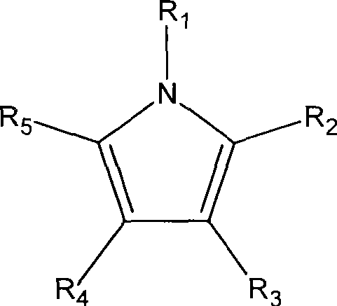
其中R1、R2、R3、R4、R5是分别选自氢或有机官能基,例如甲基(methyl)、乙基(ethyl)、丙基(propyl)、丁基(butyl)、戊基(amyl)、上述官能基的衍生或组合等。在一个范例中,R2、R3、R4、R5中各自为氢基或甲基。在其它范例中,R2、R5中各自为甲基或乙基。Wherein R 1 , R 2 , R 3 , R 4 , and R 5 are respectively selected from hydrogen or organic functional groups, such as methyl (methyl), ethyl (ethyl), propyl (propyl), butyl (butyl), Amyl (amyl), derivatives or combinations of the above-mentioned functional groups, etc. In one example, each of R 2 , R 3 , R 4 , and R 5 is a hydrogen group or a methyl group. In other examples, each of R 2 and R 5 is methyl or ethyl.
此方法更提供一种吡咯钌前驱物,其可包含第一吡咯配体与第二吡咯配体,且第一吡咯配体可与第二吡咯配体相同或不相同。或者,吡咯钌前驱物可包含第一吡咯配体与二烯配体(dienyl ligand)。例如,吡咯钌前驱物可为戊二烯吡咯钌(pentadienyl pyrrolyl ruthenium)前驱物、环戊二烯吡咯钌(cyclopentadienyl pyrrolyl ruthenium)前驱物、烷基戊二烯吡咯钌前驱物(alkylpentadienyl pyrrolyl ruthenium)或烷基环戊二烯吡咯钌(alkylcyclopentadienyl pyrrolyl ruthenium)前驱物。因此,此方法提供的吡咯钌前驱物可为烷基吡咯钌(alkyl pyrrolyl ruthenium)前驱物、双(吡咯)钌(bis(pyrrolyl)ruthenium)前驱物、二烯吡咯钌(dienyl pyrrolyl ruthenium)前驱物或上述物质的衍生物。一些范例的吡咯钌前驱物包括双(四甲基吡咯)钌(bis(tetramethyl pyrrolyl)ruthenium)、双(2,5-二甲基吡咯)钌(bis(2,5-dimethyl pyrrolyl)ruthenium)、双(2,5-二乙基吡咯)钌(bis(2,5-diethyl pyrrolyl)ruthenium)、双(四乙基吡咯)钌(bis(tetraethylpyrrolyl)ruthenium)、戊二烯四甲基吡咯钌(pentadienyl tetramethylpyrrolyl ruthenium)、戊二烯2,5-二甲基吡咯钌(pentadienyl 2,5-dimethylpyrrolyl ruthenium)、戊二烯四乙基吡咯钌(pentadienyl tetraethylpyrrolyl ruthenium)、戊二烯2,5-二乙基吡咯钌(pentadienyl 2,5-diethylpyrrolyl ruthenium)、1,3-二甲基戊二烯吡咯钌(1,3-dimethylpentadienyl pyrrolyl ruthenium)、1,3-二乙基戊二烯吡咯钌(1,3-diethylpentadienyl pyrrolyl ruthenium)、甲基环戊二烯吡咯钌(methylcyclopentadienyl pyrrolyl ruthenium)、乙基环戊二烯吡咯钌(ethylcyclopentadienyl pyrrolyl ruthenium)、2-甲基吡咯吡咯钌(2-methylpyrrolyl pyrrolyl ruthenium)、2-乙基吡咯吡咯钌(2-ethylpyrrolylpyrrolyl ruthenium)或上述化合物的衍生物。The method further provides a pyrrole ruthenium precursor, which may comprise a first pyrrole ligand and a second pyrrole ligand, and the first pyrrole ligand may be the same as or different from the second pyrrole ligand. Alternatively, the pyrrole ruthenium precursor may comprise a first pyrrole ligand and a dienyl ligand. For example, the pyrrole ruthenium precursor may be a pentadienyl pyrrolyl ruthenium (pentadienyl pyrrolyl ruthenium) precursor, a cyclopentadienyl pyrrolyl ruthenium (cyclopentadienyl pyrrolyl ruthenium) precursor, an alkylpentadienyl pyrrolyl ruthenium precursor (alkylpentadienyl pyrrolyl ruthenium) or Alkylcyclopentadienyl pyrrolyl ruthenium precursor. Therefore, the pyrrole ruthenium precursor provided by this method can be an alkyl pyrrolyl ruthenium (alkyl pyrrolyl ruthenium) precursor, a bis(pyrrole) ruthenium (bis(pyrrolyl) ruthenium) precursor, a dienyl pyrrolyl ruthenium (dienyl pyrrolyl ruthenium) precursor or derivatives of the above substances. Some exemplary pyrrole ruthenium precursors include bis(tetramethylpyrrolyl)ruthenium, bis(2,5-dimethylpyrrolyl)ruthenium, bis(2,5-dimethylpyrrolyl)ruthenium, Bis (2,5-diethylpyrrolyl) ruthenium (bis (2,5-diethyl pyrrolyl) ruthenium), bis (tetraethylpyrrolyl) ruthenium (bis (tetraethylpyrrolyl) ruthenium), pentadiene tetramethylpyrrolyl ruthenium ( pentadienyl tetramethylpyrrolyl ruthenium),
在另一个范例中,提供一种用以形成钌材料于基材上的方法,该方法包含设置一基材于具有一喷头、一等离子体隔板与一等离子体筛的等离子体增强的工艺腔体内,以及于PE-ALD工艺时连续暴露该基材至一活性试剂与一吡咯钌前驱物中。虽然等离子体可在PE-ALD工艺的任一时段中被激发,但是较佳地情况为在该基材暴露于该试剂中时激发等离子体。等离子体活化该试剂以形成一活性试剂。活性试剂的范例包含氨气等离子体、氮气等离子体与氢气等离子体。在一PE-ALD工艺的实施例中,等离子体是由工艺腔体的外部来源产生,例如由一远程等离子体产生器系统(PRS)来产生等离子体。然而,在一PE-ALD工艺的较佳实施例提供利用射频(RF)产生器的等离子体工艺腔体在原位(in-situ)产生等离子体。In another example, a method for forming a ruthenium material on a substrate is provided, the method comprising disposing a substrate in a plasma enhanced process chamber having a showerhead, a plasma baffle, and a plasma screen In vivo, as well as sequential exposure of the substrate to an active reagent and a pyrrole ruthenium precursor during the PE-ALD process. Although the plasma can be ignited at any time during the PE-ALD process, it is preferred to ignite the plasma while the substrate is exposed to the reagent. The plasma activates the reagent to form an active reagent. Examples of active reagents include ammonia plasma, nitrogen plasma, and hydrogen plasma. In one embodiment of the PE-ALD process, the plasma is generated from a source external to the process chamber, such as by a remote plasma generator system (PRS). However, preferred embodiments of a PE-ALD process provide for in-situ plasma generation in the plasma process chamber using radio frequency (RF) generators.
在另一个范例中,提供一种用以形成钌材料于基材上的方法,该方法包含设置一基材于具有一喷头、一等离子体隔板与一等离子体筛的等离子体增强的工艺腔体内,以及于热原子层沉积工艺时连续暴露该基材至一试剂与一吡咯钌前驱物中。在各种原子层沉积工艺过程中,钌材料可沉积于在基材上的阻障层(barrier layer)上(例如,铜阻障层)或介电材料(例如,低k介电材料)上。阻障层材料可包含钽、氮化钽、氮化硅钽、钛、氮化钛、氮化硅钛、钨或氮化钨。在范例中,钌材料是沉积于先前由ALD工艺或PVD工艺所形成的氮化钽材料上。介电材料可包含二氧化硅(silicon dioxide)、氮化硅(siliconnitride)、氮氧化硅(silicon oxynitride)、掺杂碳的氧化硅(carbon-doped siliconoxides)或碳氧化硅(SiOxCy)材料。In another example, a method for forming a ruthenium material on a substrate is provided, the method comprising disposing a substrate in a plasma enhanced process chamber having a showerhead, a plasma baffle, and a plasma screen The substrate is sequentially exposed to a reagent and a pyrrole ruthenium precursor in vivo, as well as during a thermal ALD process. During various atomic layer deposition processes, ruthenium materials can be deposited on a barrier layer (eg, a copper barrier layer) or a dielectric material (eg, a low-k dielectric material) on a substrate . The barrier layer material may include tantalum, tantalum nitride, tantalum silicon nitride, titanium, titanium nitride, titanium silicon nitride, tungsten or tungsten nitride. In an example, the ruthenium material is deposited on the tantalum nitride material previously formed by an ALD process or a PVD process. Dielectric materials may include silicon dioxide, silicon nitride, silicon oxynitride, carbon-doped silicon oxides, or silicon oxycarbide (SiO x C y ) Material.
可沉积导电金属于钌材料上。导电材料可包含铜、钨、铝、上述金属的合金或组合物等。在一方面,可在单一沉积工艺中形成单层的导电金属。在另一方面,也可形成多层导电金属,其中每层皆以不同的沉积工艺沉积形成。在一实施例中,利用初始沉积工艺以沉积一种晶层于该钌材料上,随后利用另一沉积工艺于该种晶层上沉积一主体层(bulk layer)。在范例中,利用无电沉积(electroless deposition)工艺、电镀工艺(ECP)或物理气相沉积工艺(PVD)以形成一铜种晶层,以及利用一无电沉积工艺、电镀工艺或化学气相沉积工艺(CVD)以形成铜主体层。在另一个范例中,利用ALD工艺或PVD工艺以形成钨种晶层,以及利用CVD工艺或PVD工艺以形成钨主体层。A conductive metal can be deposited on the ruthenium material. The conductive material may include copper, tungsten, aluminum, alloys or combinations thereof, and the like. In one aspect, a single layer of conductive metal can be formed in a single deposition process. On the other hand, multiple layers of conductive metal can also be formed, where each layer is deposited by a different deposition process. In one embodiment, an initial deposition process is used to deposit a layer on the ruthenium material, followed by another deposition process to deposit a bulk layer on the seed layer. In an example, an electroless deposition process, an electroplating process (ECP) or a physical vapor deposition process (PVD) is used to form a copper seed layer, and an electroless deposition process, an electroplating process or a chemical vapor deposition process is used (CVD) to form a copper bulk layer. In another example, an ALD process or a PVD process is used to form the tungsten seed layer, and a CVD process or a PVD process is used to form the tungsten body layer.
附图说明 Description of drawings
本发明的各项特征已于上述内容中阐述,有关本发明更特定的说明可参照附图。然而需先声明的是本发明的附图仅为代表性实施例,并非用以限定本发明的范围,其它等效的实施例仍应包含在本发明的范围中。Various features of the present invention have been described in the above content, and more specific descriptions of the present invention can be referred to the accompanying drawings. However, it should be declared that the drawings of the present invention are only representative embodiments, and are not intended to limit the scope of the present invention, and other equivalent embodiments should still be included in the scope of the present invention.
图1A至图1G绘示一本发明实施例中所述的工艺腔体的示意图;1A to 1G are schematic diagrams of a process chamber described in an embodiment of the present invention;
图2A与图2B绘示一本发明实施例中所述的隔离环的示意图;FIG. 2A and FIG. 2B are schematic diagrams of an isolation ring described in an embodiment of the present invention;
图3A与图3B绘示一本发明实施例中所述的喷头的示意图;FIG. 3A and FIG. 3B are schematic diagrams illustrating a spray head described in an embodiment of the present invention;
图4A至图4F绘示一本发明实施例中所述的水盒示意图;4A to 4F are schematic diagrams of a water box described in an embodiment of the present invention;
图5A至图5F绘示一本发明实施例中所述的等离子体隔板插件的示意图;5A to 5F are schematic diagrams of a plasma baffle insert described in an embodiment of the present invention;
图6A与图6B绘示一本发明实施例中所述的等离子体筛插件的示意图;6A and 6B are schematic diagrams of a plasma screen insert described in an embodiment of the present invention;
图7A至图7C绘示一本发明实施例中所述的绝缘套插件的示意图;7A to 7C are schematic diagrams of an insulating sleeve insert described in an embodiment of the present invention;
图8A至图8D绘示一本发明实施例中所述的气体歧管组件的示意图;8A to 8D are schematic diagrams of a gas manifold assembly described in an embodiment of the present invention;
图9A至图9D绘示一本发明实施例中所述的气体流的示意图;以及9A to 9D are schematic diagrams of gas flow described in an embodiment of the present invention; and
图10A至图10C绘示一本发明实施例中所述气体流的各种示意图。10A-10C illustrate various schematic diagrams of gas flow in an embodiment of the present invention.
其中,主要组件符号说明:Among them, the main component symbol description:
8 基材 10 轴8
20 支持控制器 22 等离子体产生控制器20 Support Controller 22 Plasma Generation Controller
30 讯号总线系统 34 导管系统30
36 真空抽气系统 37 阀门36
38 抽气口 40 基材支持件38
41 支持表面 42 端口41
44 边环 45 加热组件44
46 温度传感器 47 间隙46
48a、48b、48c 内边环 50 工艺腔体48a, 48b, 48c
51 控制单元 52 中央处理单元(CPU)51
54 支持电路 56 内存54
58 相关控制软件 59 内腔体区域58 Related control software 59 Inner cavity area
60 工艺区域 61 阻气间隙60
62 上表面 70a-e 气体源62
72a-72e 阀门组件 80 腔体主体72a-
82 隔离环衬垫 84 腔体衬垫82 Spacer gasket 84 Cavity gasket
88 射频带 90 腔体主体组件88 Radio Frequency Band 90 Cavity Body Components
92 等离子体产生器系统 94 射频尖端92
95a-b 绝缘体 96 匹配件95a-
97 等离子体产生器 98 连接器97
100 盖组件 101 调准狭缝100
102 下表面 103 盖支持件102
104 上表面 106 把手104
107 把手组件 108 热隔离体107
110 支持托架 116-118 端口110 support bracket 116-118 ports
119 孔 120 开口119
122 凸缘表面 124 壁表面
200 隔离环 202a-d 下表面200
204 上表面 205a-d 内表面204
220 开口 300 喷头220
302a-c 下表面 303-304 上表面302a-c lower surface 303-304 upper surface
305a-b 壁表面 306 上表面305a-
310 孔 320 开口310
322 凸缘 324 上表面322
328 环 330 环组件328
332 凸缘 350 接触332
400、400c-f 水盒 402a-c 下表面400, 400c-
403、404 上表面 405 内表面403, 404
410 入口 411 喷嘴410
412 出口 413 喷嘴412
414a-b 凸缘表面 416a-c 内表面414a-
420 开口 421 源喷嘴420
423 返回喷嘴 425、427 线路423
430 通路 432c 讯号线圈430 access 432c signal coil
432d 多线圈 432e 分支或支线线圈432d Multi-coil 432e Branch or branch coil
440 通路 441 气体区域440
450 接触 500 等离子体隔板插件450
501 沟槽 502 下表面501
503 上表面 504 下表面503
505 上表面 506 开口505
508 开口 510 狭缝508
512 下边缘 513 间隙512
514 上边缘 515 径向线514 Upper edge 515 Radial line
520 头锥 522 锥表面520
526a 上通路 526b 下通路526a
528 阻气门 530 孔528
531、532、535、537 线 533 径向线531, 532, 535, 537
538 轴向线 539 虚线圆形538
540 气体区域 600 等离子体筛插件540
601 中央部分 602 上表面
601
603 下表面 604 上表面603
605a-b 内壁表面 606 上表面605a-b
608 上表面 612 孔608
614 狭缝 622 沟槽614
624、626 壁表面 630 内部区域624, 626
631 环组件 632 外部区域631
640 气体区域 700 绝缘套640
703a-e 下表面 704 上表面703a-e
707 孔 710、720 通道707
721 上部分 722 扩展通道721
723 下部分 725 凹槽723
726 孔 742 气体726
744 气体区域 780 夹钳744
782 绝缘部 784 金属夹钳部782
800 气体歧管组件 806 歧管档块800
808 隔离体 810 通道808
811 气体入口 813 气体入口811
814 凸缘 815 气体入口814
816 壁表面 820 通道816
821 通道导管 822 包围镜片821
823 通道导管 824 镜片边环823
825 表面 826 窗口组件825
830 气体导管组件 831 导管830
832、834 凸缘 836 导管832, 834
838 导管 840 导管组件838
842 下歧管 843 孔842
844 上歧管 850 歧管套组件844
852、854 气体通道支持件 880、882、884 气体导管852, 854
910 气体区域 912、914 流动型态910
915a-c 中央线 916 流动型态915a-
917 径向线 918 流动型态917
920 气体区域 922、922a-c 流动型态920
923 环形路径 950 区域923
1021 通道导管 1082、1084 导管1021
1086 导管1086 Conduit
具体实施方式 Detailed ways
本发明实施例提供一种可在原子层沉积工艺(ALD),或较佳在等离子体增强的原子层沉积工艺(PE-ALD)过程中沉积材料的设备。本发明的其它实施例提供于工艺腔体中形成材料的工艺。在实施例中,工艺腔体是用以进行等离子体增强的原子层沉积工艺并具有多个电性绝缘、接地或高频热的零件。在范例中,腔体主体与气体歧管组件是接地且以例如绝缘套、等离子体筛插件与隔离环等电性绝缘零件分隔开来。一喷头、一等离子体隔板与一水盒是设置在这些绝缘零件之间,且在受到等离子体产生器启动时,会具有射频热(RF hot)。An embodiment of the present invention provides an apparatus capable of depositing materials during atomic layer deposition (ALD), or preferably, plasma enhanced atomic layer deposition (PE-ALD). Other embodiments of the invention provide processes for forming materials in process chambers. In an embodiment, the process chamber is used for plasma-enhanced atomic layer deposition process and has a plurality of electrically isolated, grounded or high-frequency thermal parts. In one example, the chamber body and the gas manifold assembly are grounded and separated by electrically insulating components such as insulating sleeves, plasma screen inserts, and isolation rings. A shower head, a plasma partition and a water box are arranged between these insulating parts, and will have radio frequency heat (RF hot) when activated by the plasma generator.
硬件hardware
图1A至图1G绘示盖组件100的示意图,其可用以进行各种原子层沉积工艺。在实施例中,工艺腔体50可于热原子层沉积工艺或等离子体增强的原子层沉积工艺时形成材料于基材8上。图1A绘示工艺腔体50的剖面图,其可用以制作集成电路。工艺腔体50包含连接至腔体主体组件90的一盖组件100。处理基材的工艺区域60于是形成并通常位于盖组件100与腔体主体组件90之间,更明确来说,工艺区域60是位于基材支持件40的支持表面41与基材8的正上方以及位于上表面62的正下方。在一实施例中,在上表面62与支持表面41之间的腔体间隔(spacing)是介于约0.5毫米至约50毫米之间,较佳介于约1毫米至12毫米之间,更佳是介于约4毫米至8毫米之间,例如5.84毫米(0.23英时)。视沉积工艺中不同的输送气体与工艺条件,可改变该间隔。1A to 1G are schematic diagrams of a
基材支持件40包含边环(edge ring)44与加热组件45(图1A与图1G)。加热组件45是嵌入于基材支持件40内。边环44是设置在基材支持件40的周围并位于基材支持件40的上部位上。内边环48a、48b、48c是位于加热组件45上,且位于边环44覆盖住该基材支持件40的上部位的该区段下方。边环44可当作清洗环(purge ring),以引导边缘清洗气体由基材支持件40处通过位于内边环48a、48b、48c之间的间隙47、边环44与加热组件45,最后通过基材8的边缘上方(图1G)。边缘清洗气体流可避免反应性工艺气体扩散至加热组件45处。The
阻气间隙(choke gap)61是形成在边环44与上表面62之间的环绕间隙或间隔,更明确而言,是形成在边环44的上缘表面与隔离环200的下表面202d之间。靠着部分分开工艺区域60与内部腔体区域59的非均匀压力分布区,阻气间隙61也有助于在工艺区域60内提供更均匀压力分布。阻气间隙61可视工艺条件与所需的抽气效率而改变。利用调整阻气间隙61,可控制沉积工艺过程中的抽气效率。降低基材支持件40即可增加阻气间隙61,而升高基材支持件40可减少阻气间隙61。通过改变阻气间隙61的距离,可调整从位于工艺腔体50下部位的抽气口38(pumping port)至通道820中央间的抽气传导(pumping conductance),来控制在沉积工艺中膜的厚度与均匀性。在一实施例中,上方阻气间隙61的间隔是介于约0.5毫米至约50毫米之间,较佳地介于约1毫米至5毫米之间,更佳地是介于约2.5毫米至4毫米之间,例如33毫米(0.13英时)。A
在一实施例中,抽气传导的压差可加以控制,以减少或消除次级等离子体的生成。因为等离子体的生成与维持是与离子浓度相关,所以可减少在特定区域内的压力以将离子浓度最小化。因此,可避免次级等离子体生成于工艺腔体的特定区域中。在一较佳实施例中,工艺腔体50是用以进行PE-ALD工艺。因此,整个工艺腔体50内的各个区域与零件是电性绝缘、接地或具有高频热。在一范例中,腔体主体80与气体歧管组件800是接地且以电性绝缘的隔离环200、等离子体筛插件600以及绝缘套700加以分隔。在电性绝缘零件之间的喷头300、等离子体隔板插件500以及水盒400在受等离子体产生器系统92(第1E图)启动时会具有高频热。工艺腔体50也包含绝缘环衬垫(insulator ring liner)82、腔体衬垫84与其它绝缘衬垫,以减少或完全消除任何在上表面62与腔体主体组件90之间的可直视性(line-of-sight)。绝缘衬垫有助于减少或消除等离子体对腔体主体组件90的金属表面的腐蚀作用。因此,当产生等离子体时,基材支持件40与位于其上的晶片是与喷头300成为一接地通路(grounded path)。In one embodiment, the differential pressure across the evacuation can be controlled to reduce or eliminate secondary plasma generation. Since the generation and maintenance of the plasma is ion concentration dependent, the pressure in a particular region can be reduced to minimize the ion concentration. Therefore, generation of secondary plasma in certain regions of the process chamber can be avoided. In a preferred embodiment, the
参照图1A,因为工艺区域60与内部腔体区域59隔离开来,反应气体或清洗气体仅需要足以填充工艺区域60的量,以确保基材8能充分暴露于反应气体或清洗气体中。在公知的化学气相沉积工艺中,需要工艺腔体以同时并均匀地提供由数种反应物所构成的组合气流至整个基材表面上,以确保这些反应物的反应在基材8表面上均匀发生。在ALD工艺中,工艺腔体50是用以使基材8连续接触诸如气体或等离子体的化学反应物,这些化学反应物是如同一薄层般地吸附或发生反应于基材8的表面上。于是,ALD工艺不需要反应物同时到达基材8的表面。反而所提供的反应物量仅需要足以吸附在基材8表面而形成一薄层或足以与基材8表面上的吸附薄层发生反应的量。Referring to FIG. 1A , since the
相较于公知CVD腔体的内部容积,工艺区域60包含一较小体积,所以在ALD程序的特定工艺中需要用来填充工艺区域60的气体量较少。因为内腔体区域具有大约20升的体积,工艺区域60是与内腔体区域59分开以形成较小体积,例如大约3升或更小,较佳约2升,更佳约1升或更小。在一个适合处理直径200毫米的基材的腔体中,工艺区域60约为1000立方厘米或更小,较佳约500立方厘米或更小,更佳约为200立方厘米或更小。在一个适合处理直径300毫米的基材的腔体中,工艺区域60大约为3000立方厘米或更小,较佳约1,500立方厘米或更小,更佳约为1000立方厘米或更小,例如约800立方厘米或更小。在一个适合处理直径为300毫米的基材的腔体实施例中,工艺区域60的体积大约为770立方厘米或更小。在另一个实施例中,可升高或降低基材支持件40以调整工艺区域60的体积。例如,升高基材支持件40以形成体积具有770立方厘米或更小的工艺区域60。越小的工艺体积在工艺中需要注入工艺腔体50中的气体越少(例如,工艺气体、载气或清洗气体)。由于用来供应与移除气体的时间较短,所以工艺腔体50的产量可较大,且因为使用较少量的气体,减少化学前驱物与其它气体的浪费,因而降低运作成本。The
图1B进一步显示盖组件100与其零件的分解图。具有下表面102与上表面104的盖支持件103可由各种材料所形成,包括金属材料。较佳地,盖支持件103是由金属所形成,诸如铝、钢、不锈钢(例如,可选择性包含镍的铁铬合金)、铁、镍、铬、上述金属的合金或组合物等。盖组件100可通过铰炼(hinge,未显示)而连结至腔体主体组件90上。一旦盖组件在闭合位置上时,于盖支持件103上的调准狭缝101是与连结至腔体主体组件90的一杆(post,未显示)对准。盖支持件103也包含位于上表面104的支持托架(support bracket)110与把手组件(handle assembly)107。把手组件107可包含一热绝缘体108,其位于把手106与上表面104之间。再者,盖组件100具有突出表面(ledge surface)122与壁表面(wall surface)124。多个孔与开口,例如端口116、117与118,也可贯穿盖支持件103而可提供供导管、软管、扣件(fasteners)、器具与其它装置的通路。盖支持件103更包含未贯穿的孔。例如,孔119可带有螺纹状,且用以接收诸如螺丝或螺栓等扣件。FIG. 1B further shows an exploded view of the
盖组件100更包含隔离环200、喷头300、水盒400、等离子体隔板插件500、等离子体筛插件600、绝缘套700以及气体歧管组件800。盖组件100的每个零件(即,隔离环200、喷头300、水盒400、等离子体隔板插件500、等离子体筛插件600、绝缘套700或气体歧管组件800)的尺寸大小可加以改变以处理各种尺寸的基材,例如直径为150毫米、200毫米、300毫米或更大的晶片。再者,可设置每个零件并以夹钳(clip)780固定在盖支持件103上。夹钳780在水盒400的上表面404上方夹紧,且以穿过孔119的扣件将其固定住(图1A至图1G)。在范例中,夹钳780包含金属夹钳部(metal clipsegment)784,其位于绝缘部(insulator segment)782上。绝缘部782可由电性绝缘材料、绝热材料或上述材料的组合所形成。当夹钳780固定盖组件100的各种零件时,绝缘部782在上表面404与盖支持件103之间提供电性绝缘与热绝缘。当调准时,轴10会通过盖组件100的中央,包含通过盖支持件103的开口120、隔离环200的开口220、喷头300的开口320、水盒400的开口420、等离子体隔板插件500的头锥520、等离子体筛插件600的中央部位601、绝缘套700的通道720以及气体歧管组件800的信道820。The
图1C绘示在盖组件100与轴10下方的视图以显示盖支持件103的上表面62与下表面102。工艺区域60的上表面62是由隔离环200的下表面202d与205d、喷头300的下表面302c以及等离子体隔板插件500的下表面502所共同形成。基材8是位于工艺区域60内的下表面62下方,且在沉积工艺中暴露在工艺气体下。在一实施例中,于ALD工艺时是相继暴露基材于至少两种工艺气体中(例如,气体或等离子体)。在ALD工艺的范例中,基材8是暴露在来自等离子体隔板插件500的狭缝510的第一工艺气体中,以及暴露在来自喷头300的孔310的第二工艺气体中。FIG. 1C depicts a view below the
沿着轴10的视图进一步显示,尽管在下表面502处可看见狭缝510的开口508,但看不见狭缝510的另一端,例如在上表面503的开口506(图5C)。此轴10下方的阻碍视图是起因于狭缝510的角度(图5B中的角度α1),其显示位于等离子体隔板插件500上方介于工艺区域60与气体区域640之间的通路无法直视到底。在工艺区域60与气体区域640之间具有受阻路径较可直视到底的未受阻路径具有更多优点,包含减少或消除在等离子体隔板插件500内或上方的次级等离子体。The view along the
在本文中所使用的「直视」(Line-of-sight)是指在两点之间的直通路径或实质直通的路径。该直通路径或实质直通路径为至少两点之间的气体或等离子体提供未受阻碍或畅通的通路。一般来说,受阻碍或不直通(obscured)的通路可允许气体通过同时阻止或实质减少等离子体通过。因此,直视性通路通常允许气体或等离子体通过,而在两点间不具直视性的通路则阻止或实质减少等离子体通过但允许气体通过。As used herein, "Line-of-sight" refers to a straight path or a substantially straight path between two points. The through path or substantially through path provides an unimpeded or unimpeded passage for gas or plasma between at least two points. In general, an obstructed or obscured passageway allows the passage of gas while preventing or substantially reducing the passage of plasma. Thus, a line-of-sight pathway generally allows the passage of gas or plasma, while a non-line-of-sight pathway between two points prevents or substantially reduces the passage of plasma but allows the passage of gas.
在一实施例中,可将上表面62的一部份,称其为下表面(lowersurface)302c与下表面502,予以粗糙化(例如,透过机械加工)以使上表面62具有更多的表面积。上表面62增加表面积可增加沉积工艺中累积材料的附着度,并因为减少累积材料的剥落进而减少污染。在范例中,下表面302c与下表面502各自的平均粗糙度(Ra)可至少约15微英时(大约0.38微米),较佳地约100微英时(约2.54微米),更佳约200微英时(约5.08微米)或更高。盖支持件103的下表面102也可粗糙化,以具有至少大约15微英时(约0.38微米)的粗糙度,较佳为至少约50微英时(约1.27微米),例如大约54微英时(约1.37微米)。In one embodiment, a portion of upper surface 62, referred to as
图1B与图1D进一步绘示出气体歧管组件800,其包含导管组件840、歧管套组件850与气体导管组件830。歧管套组件850具有可观察激发等离子体的窗口组件826(图1A)。或者,歧管套组件850可包含不具窗口的表面825(图1D)。当气体导管组件830可在凸缘834处与端口117连接且流体连通,同时气体导管组件830延伸至与歧管档块(manifold block)806上的气体入口813连接且流体连通(图1D与图8D)。FIGS. 1B and 1D further illustrate the
在一实施例中,等离子体产生器系统92是借着射频带(RF strap)88而连结至盖组件100上(图1D)。一部份的等离子体产生器系统92,称其为射频尖端(RF stinger)94与绝缘体95a,突出并穿通位于盖支持件103上的端口116且连接至喷头300与水盒400。当RF带将RF尖端94电性连接至区域950时,绝缘体95a使RF尖端94与盖支持件103电性绝缘,其中该区域950包含位于喷头300与水盒400上的接触点(contact)350与450。RF尖端94为诸如金属杆或电极等导电材料,其包含铜、黄铜(brass)、不锈钢、钢、铝、铁、镍、铬、上述金属合金、其它导电材料或上述材料的组合。In one embodiment, the
等离子体产生器系统92更包含等离子体产生器97,其安装于腔体主体80下方(图1E)。绝缘体95b位于等离子体产生器97与腔体主体80之间以电性隔离等离子体产生器97。匹配件96可突出贯穿绝缘体95b且与腔体主体80电性接触。等离子体产生器97更包含连接器98。在一范例中,连接器98是为RF共轴缆线连接器(RF coaxial cable connector),例如N型连接器。等离子体产生器系统92可通过连接至讯号总线系统(signal bus system)30的等离子体产生控制器(plasma generator controller)22来操作。在一个范例中,等离子体产生器系统92的工艺条件可设定以在电压约300瓦、电流约9安培的条件下具有大约4欧姆(ohms)的腔体阻抗。等离子体系统与工艺腔体可与盖组件100一同使用或可当作等离子体产生器系统92使用,以及腔体主体组件90是为可在加州圣塔克拉拉的应用材料公司(Applied Materials,Inc)购得的
工艺腔体50的腔体主体组件90包含绝缘环衬垫82,其用以降低等离子体接触腔体主体80且有助于将等离子体局限在工艺区域60中(图1F)。再者,腔体主体组件90通常罩盖住基材支持件40,该支持件40连结至位于内腔体区域59的杆42上。使用支持控制器20可使基材支持件40在工艺腔体50内的垂直方向移动。在实施例中,基材支持件40是可转动。工艺区域60位于基材支持件40的上方与盖组件100的下方,较佳是至少位于喷头300、等离子体隔板插件500与部分的隔离环200下方。Chamber body assembly 90 of
视特定工艺而定,于预处理步骤、沉积步骤、后处理步骤或其它在制作过程中使用的工艺步骤之前或当中,可加热基材8至某特定温度。例如,可利用嵌入式加热组件45以加热基材支持件40。通过施加来自交流电源的电流至加热组件45,可以电阻加热方式来加热基材支持件40。基材8是因基材支持件40而受热。另一个方式为透过诸如灯管(未显示)的辐射热源以加热基材支持件40。Depending on the particular process,
也可将例如热偶计(thermocouple)等温度传感器46嵌入基材支持件40内以监测基材支持件40的温度。所测量的温度是用于前馈回路中以控制供应至加热组件45的交流电源供应,如此基材8的温度便可加以维持或控制在特定工艺的需求温度。基材升降插梢(lift pin)(未显示)也可嵌入至基材支持件40中以使基材由支持件表面41处升高。A
真空抽气系统36是用以排空并维持在工艺腔体50内的压力(图1F)。真空抽气系统36通过抽气端口38与阀门37而与工艺腔体50连接。气体歧管组件800位于基材支持件40的上方,而工艺气体透过该气体歧管组件800进入工艺腔体50中。气体歧管组件800可连接至气体面板(gas panel)上,其控制并供给各种工艺气体注入工艺腔体50中。The
气体源70a、70b、70c、70d、与70e提供前驱物气体、载气或清洗气体通过导管系统34进入工艺腔体50中。气体源70a、70b、70c、70d、与70e可直接或间接地连接至一化学供给或一气体供给。化学或气体供给包含储槽(tank)、安瓿(ampoule)、鼓泡器(bubbler)、喷雾器(vaporizer)或其它可储存、传送或形成化学前驱物的容器。化学或气体供给也可来自内部来源。连接至控制单元51的阀门组件72a、72b、72c、72d与72e可适当地控制与调节来自气体源70a、70b、70c、70d、与70e的气体流进入气体歧管组件800。气体歧管组件800能引导工艺气体进入工艺腔体50中,并且可选择性加热该歧管组件以避免任何气体凝结在歧管组件800的导管或管线内。
每个阀门组件72a、72b、72c、72d与72e可包含隔板(diaphragm)与阀座(valve seat)。可各自采用施加偏压或机械启动(actuated)的方式开启或关闭隔板。隔板可以气动或电子方式启动。气动阀门可于Fuiikin与Veriflow公司购得,而电子启动阀门可于Fujikin公司购得。控制单元51可耦接至阀门组件72a、72b、72c、72d与72e以控制阀门隔板的启动。气动阀门可提供时距大约0.02秒的气体脉冲。电子启动阀门可提供时距大约0.005秒的气体脉冲。一般而言,气动阀门与电子启动阀门可提供时距高达大约3秒的气体脉冲。虽然较高时距的气体脉冲是可行的,但是典型ALD工艺使用用来产生气体脉冲的ALD阀门在阀门开启的时距大约为5秒或更短,较佳大约为3秒,更佳大约为2秒或更短。在一实施例中,ALD阀门脉冲开合的时间间隔介于约0.005秒至3秒之间,较佳介于约0.02秒至约2秒之间,更佳介于约0.05秒与1秒之间。电子启动阀门通常需要耦接在阀门与控制单元51之间的驱动器。在另一个实施例中,每个阀门组件72a、72b、72c、72d与72e可包含质量流量控制器(MFC)以控制气体散布、气体流速与其它ALD脉冲程序相关因素。Each
在ALD设备内的前驱物或气体输送系统是用以储存与输配化学前驱物、载气、清洗气体或上述气体的组合物等。输送系统可包含阀门(例如,ALD阀门或质量流量控制器)、导管、储存器(reservoirs)、安瓿与鼓泡器、加热器以及/或控制单元系统,其可与工艺腔体50或盖组件100一起使用并与气体歧管800或导管系统34流体连通。在范例中,输送系统可包含气体源70a~70e以及连接至控制单元51的阀门组件。用于ALD工艺的输送系统是阐述在共同受让且审理中的美国专利申请案11/127753中,该案在2005年5月12日申请,名称为「用于含铪高k材料的原子层沉积的设备与方法」(Apparatus and Methods for Atomic Layer Deposition of Hafnium-ContainingHigh-k Materials),公开号为2005-0271812;于2005年4月29日申请的美国专利申请案11/119388,名称为「控制气流与输送以抑制微粒在MOCVD/ALD系统中生成的方法」(Control of Gas Flow and Delivery to Suppress theFormation of Particle in an MOCVD/ALD System),其公开号为2005-0252449;于2002年10月25日申请的美国专利申请案10/281079,名称为「用于原子层沉积的气体输送设备」(Gas Delivery Apparatus for AtomicLayer Deposition),其公开号为2003-0121608;以及2003年11月3日申请的美国专利申请案10/700328,名称为「具有流速控制的前驱物输送系统」(Precursor Delivery System with Rate Control),其公开号为2005-009859,在此是以参考方式纳入该些参考文献的内容。The precursor or gas delivery system in the ALD equipment is used to store and deliver chemical precursors, carrier gases, purge gases or combinations thereof. The delivery system can include valves (e.g., ALD valves or mass flow controllers), conduits, reservoirs, ampoules and bubblers, heaters, and/or control unit systems that can be integrated with the
诸如个人计算机或工作站计算机等控制单元51可耦接至工艺腔体50上以控制工艺条件。例如,控制单元51可设计在基材工艺程序的不同阶段中控制各种工艺气体与清洗气体由气体源70a-70e处通过阀门组件72a-72e。例如,控制单元51包含中央处理单元(CPU)52、支持电路(support circuitry)54与具有相关控制软件58的内存(memory)56。A
软件例程可储存在内存56中或由一远程来源(例如,计算机或服务器)所执行。执行软件例程以启动工艺配方或程序。当执行软件例程时,普通计算机将转换成在腔体工艺过程中控制腔体运作的特定工艺计算机。例如,于执行根据本文中所述实施例的工艺程序时,软件例程可透过操作阀门组件72a-72e而精确控制气体源70a-70e的启动。或者,软件例程可在硬件中执行,例如特定用于集成电路的硬件或其它型式的硬件或是软件与硬件的组合等。The software routines may be stored in
控制单元51可以是任何一种可用于工业设定以控制各种反应室与次处理器的普通计算机处理器。CPU 52可利用任何合适的内存56,例如随机存取内存、只读存储器、软盘机、光驱、硬盘或其它内部或远程的数字储存形式。各种支持电路可耦接至CPU 52上以支持工艺腔体50。控制单元51可耦接至邻近独立腔体零件的其它控制器,例如阀门组件72a-72e的程序逻辑控制器。控制单元51与工艺腔体50的其它零件之间的双向沟通是由多个集合的讯号缆线,也就是讯号总线30所处理,有些总线是绘示于图1F中。除了控制来自气体源70a-70e的工艺气体与清洗气体之外,阀门组件72a-72e、任何程序逻辑控制器与控制单元51可负责自动控制在制造工艺中的其它动作。控制单元51是连接至等离子体产生器控制器22、真空抽气系统36以及包含温度监控、控制与升降插梢(未显示)控制的支持控制器(supportcontroller)。The
隔离环200包含开口220(图2A与图2B)且位于喷头300与盖支持件103之间(图1A与图1B)。隔离环200包含上表面204以支持喷头300。开口220可与开口120对准,使得轴10通过该些开口的中央。隔离环包含朝轴10向内逐渐变细的内表面205a、205b、205c与205d。
隔离环200更包含下表面202a、202b、202c与202d。当支撑住隔离环200时,下表面202a可用以接触盖支持件103的凸出表面(ledge surface)122。当下表面202d与205d为上表面62的一部份时,下表面202d与205d形成工艺区域60。上表面62中由下表面202d所形成该部份是在工艺区域60与内腔体区域59之间形成外环密封(outer ring seal)。隔离环200可由能抵抗等离子体或抵抗工艺反应物的电性绝缘材料所形成。隔离环200也可包含热绝缘材料。可作为隔离环200的材料包含陶瓷、石英、熔融石英块、蓝宝石、热解氮化硼(pyrolytic boron nitrite,PBN)材料、玻璃、塑料、上述材料的衍生物或组合等。The
喷头300包含开口320(图3A与图3B)且可位于隔离环200与水盒400之间(图1A与图1B)。喷头300包含上表面303、304与306,其中上表面304与306可用以支撑水盒400。壁表面305a与305b位于上表面303、304与306之间。喷头300更包含下表面302a、302b与302c。当支撑住喷头300时,下表面302a可当作隔离环200的上表面204。当下表面302c成为上表面62的一部份时,其也形成工艺区域60(图1C)。喷头300可由各种材料所形成,包含金属或其它导电材料。较佳地,喷头300是由金属所形成,例如铝、钢、不锈钢、铁、镍、铬、上述金属的合金或组合等。The
开口320贯穿喷头300且与开口120与220对准,使得轴10可通过每个开口的中央(图1B)。再者,开口320贯穿环组件330。环组件330位于喷头300的中央且可用以容纳等离子体隔板插件500。环组件330包含设置在上表面303表面上方的环328。凸出部(ledge)332由环328处向内朝轴10的方向突出,且用以支撑等离子体隔板插件500于凸出部332上。凸出部322由环328处以远离轴10的方向向外突出且用以配合上表面304与306一同支撑水盒400。环328的上表面324是用以支撑等离子体筛插件600。
喷头300的上表面303接收工艺气体,并透过孔310而输送至工艺区域60中。孔310从上表面303贯穿喷头300至下表面302c处以提供两处之间的流体连通。在喷头300中的孔310直径介于约0.1毫米与约1毫米之间,较佳地是介于约0.2毫米与0.8毫米之间,更佳地介于约0.4毫米至0.6毫米之间。喷头300可具有至少约100个孔,较佳地具有约1000个孔,更佳具有约1500或更多个孔。视孔310的大小、孔310的分布状况、基材大小与所需的暴露速率而定,喷头300可具有多达6000个孔或10000个孔。多个孔310之间可具有不同或一致的几何形状。在范例中,喷头300由金属所构成(例如,铝或不锈钢),且具有1500个直径为0.5毫米的孔。The
喷头300包含开口320(图3)且位于隔离环200与水盒400之间(图1A与图1B)。喷头300包含上表面303、304与306,其中上表面304与306可用以支撑水盒400。壁表面305a与305b介于上表面303、304与306之间。喷头300更包含下表面302a、302b与302c。当支撑喷头300时,下表面302a可当作隔离环200的上表面204。当下表面302c作为上表面62的一部份时,其也形成工艺区域60(图1C)。喷头300可由各种材料所形成,包含金属或其它导电材料。较佳地,喷头300是由金属所形成,例如铝、钢、不锈钢、铁、镍、铬、上述金属的合金或组合物等。The
多个孔310是贯穿形成于喷头300中,使得上表面303与下表面302c间流体连通。孔310可具有各种大小且以多种图案散布在上表面303与下表面302c上。每个孔310的直径介于约0.1毫米至约1毫米之间,较佳地是介于约0.2毫米与0.8毫米之间,更佳地介于约0.4毫米至0.6毫米之间,例如约0.51毫米(0.02英时)。喷头300可具有至少约100个孔,较佳地具有约1000个孔,更佳地是具有约1500或更多个孔。视孔310的大小、孔310的分布状况、基材大小与所需的暴露速率而定,例如,喷头300可具有6000个孔或10000个孔。较佳地,喷头300由金属所构成(例如,铝或不锈钢)且具有1500个直径为0.5毫米的孔。A plurality of
包含开口420的水盒400(图4A与图4B)可位于喷头300(图1A与图1B)的顶端且通过移除盖组件100的热而调节温度。开口420包含凸出表面414a与414b以及内表面416a、416b与416c。多个通路440由内表面416b处放射状地向内延伸贯穿水盒400直到下表面402c处。开口420是用以接收等离子体隔板插件500、等离子体筛插件600、绝缘套700。绝缘套700可位于凸出表面414a上。水盒400可由各种包含金属的材料所形成。较佳地,水盒400是由金属所形成,例如铝、钢、不锈钢、铁、镍、铬、上述金属的合金或组合物等。水盒400的下表面402a、402b是置于喷头300的上表面304与306上。水盒400也包含上表面403,其被具有上表面404的内表面405所包围。水盒400有助于移除盖组件100的热,尤其是喷头300处的热。上表面403包含入口410与出口412,该入口410与出口412与通路430间流体连通。在沉积工艺中,具有初期温度的流体是通过入口410而供应至水盒400处。当流体行经通路430时,流体可吸收热。具较高温度的流体可经由出口412而自水盒400处移除。A water box 400 ( FIGS. 4A and 4B ) including an
流体可为液态、气态或超临界状态,其可适时吸收并驱散热量。可用于水盒400中的液体包含水、油、酒精、乙二醇、乙二醇醚类、其它有机溶剂、超临界流体(例如二氧化碳)、上述液体的衍生物或混合物等。气体可包含氮气、氩气、空气、氢氟碳化合物(HFCs)或上述气体的组合物。较佳地,提供给水盒400的流体是水或水/酒精混合物。Fluids can be liquid, gaseous or supercritical, which absorb and dissipate heat in due course. Liquids that can be used in the
入口410可用以接收连接至线路425(例如,软管(hose))的喷嘴411,该线路425与流体源流体连通。同样的,出口412可用以接收连接至线路427(例如,软管)的喷嘴413,该线路427与流体回收处(fluid return)流体连通。流体源与流体回收处可以是内部冷却系统或独立的冷却系统。线路425与427连接至来源喷嘴421以及返回喷嘴423,该些喷嘴通过支持件托架110而固定在盖支持件103上。线路425与427可为圆管(tube)、软管、导管或线路。The
在实施例中,供给至水盒400的流体具有介于约-20℃至约40℃的温度,较佳地介于约0℃至约20℃。可调整温度、流速与流体组成以适度移除包含喷头300的盖组件100的热,同时将水盒400保持在预定温度。水盒400可维持在预设温度内,此预定温度介于约0℃至约100℃之间,较佳介于约18℃至约65℃之间,更佳介于约20℃至约50℃之间。In an embodiment, the fluid supplied to the
在另一实施例中,图4C至图4F绘示可用以取代通路430的不同几何形状的通路430c、430d、430e与430f。通路430c-430f可包含围绕开口420的部分循环(loop)432c(图4C)、单一循环432d(图4D)、多循环432e(图4E)或包含分支或支线432f(图4F)。In another embodiment, FIGS. 4C-4F illustrate vias 430 c , 430 d , 430 e , and 430 f of different geometries that may be used in place of via 430 . Pathways 430c-430f may include a partial loop 432c (FIG. 4C), a
气体区域540是位于喷头300的上表面303上方以及水盒400的下表面402c下方。通路440由内表面416b延伸贯穿水盒400并进入气体区域540。内表面416b可向内弯曲凹陷以形成气体区域441,该气体区域441位于内表面416b、等离子体筛插件600以及绝缘套700之间(图7C)。气体区域441包围等离子体筛插件600以维持与狭缝614间的流体连通。通路440在气体区域441与540之间提供流体连通。水盒400包含数个通路440。例如,水盒400可包含至少10个通路,较佳包含至少24个通路,更佳包含至少36个通路或更多。The
图5A至图5F绘示等离子体隔板插件500的示意图,如一些实施例中所述般,其可作为盖组件100的一部份。等离子体隔板插件500是用以接收来自气体区域640的工艺气体,并输配或送出工艺气体至工艺区域60中。较佳地,等离子体隔板插件500是以一预设角度来输配工艺气体。下表面503包含多个狭缝510,这些狭缝510延伸贯穿等离子体隔板插件500直到下表面502,以输配工艺气体至工艺区域60中。5A-5F are schematic diagrams of a
等离子体隔板插件500是如图所示般包含头锥520,其由上表面503处延伸至锥表面522(图5A)。锥表面522可具有各种几何形状,例如平面(图5B),或者头锥520可延伸至一点(未显示)。较佳地,锥表面522是实质水平以接触等离子体筛插件600。头锥520可延伸至气体区域640中,该气体区域640形成在等离子体隔板插件500上方、等离子体筛插件600下方以及环组件330内。头锥520在气体区域640内占有一预定体积。若头锥520占据较大体积,则在沉积工艺中需要用来填充气体区域640的工艺气体量较少。于是,因为在每次ALD工艺的半周期中可较快地供给或移除在气体区域640中的工艺气体,因此可具有较短的ALD周期。
等离子体隔板插件500包含具有下表面502的下边缘(lower rim)512,以及具有上表面505与下表面504的上边缘514。下边缘512与上边缘514是以间隙513分隔开来。可设置一衬垫(gasket)在间隙513内以提供较佳导电性或较佳密封。衬垫可包含O型环(O-ring)或密封剂(sealant)。较佳地,衬垫是为RF衬垫且包含导电材料,例如金属缆线或掺杂导电材料的聚合物。在一较佳实施例中,诸如缠绕的不锈钢缆线等RF衬垫是沿着间隙513设置,以提供与喷头300间的导电接触。等离子体隔板插件500可位于喷头300的开口320内,以使上边缘514的下表面504位于喷头300的凸出部332上(图1A与图1B)。等离子体隔板插件500也被环组件330所围绕而位于开口320内。等离子体隔板插件500是由例如铝、钢、不锈钢、铁、镍、铬、其它金属、上述金属的合金或组合物所构成。The
等离子体隔板插件500包含多个狭缝510,使得上表面503的开口508与下表面502的开口506间流体连通(图5与图5C)。这些狭缝510提供使工艺气体以一预定角度由气体区域640流入工艺区域60的信道。理想状况为,狭缝510引导工艺气体以喷射角α1的角度接触基材8或支持件表面41,该角度是从轴10至线段532之间所测得的角度。当线段532沿着狭缝510的平面延伸,同时轴10垂直通过下表面502。因此,位于等离子体隔板插件500内的狭缝510是设置成喷射角α1,并以引导具有工艺气体具有喷射角α1角度的流动型态,如图5C与图9C至图9D所示。
在一些实施例中,等离子体隔板插件500可包含沟槽(trough)501或多个孔530,以助于移动上表面503的工艺气体。在实施例中,如图5A至图5C所示般,等离子体隔板插件500可包含围绕在狭缝510外径的沟槽501。或者,狭缝510可延伸至沟槽501中(未显示)。In some embodiments, the
在另一个实施例中,如图5D至图5F所示般,等离子体隔板插件500可包含多个围绕在头锥520外径的孔530。每个孔530沿着轴线538由上表面503延伸至下表面502。在范例中,每个孔530沿着轴线538具有固定直径。较佳地,每个孔530包含以阻气门528分隔开来的上通路526a与下通路526b。上通路526a的通常直径大于下通路526b的直径。In another embodiment, as shown in FIGS. 5D-5F , the
在一些实施例中,具有与支持件表面41水平或垂直的流动型态(即,喷射角α1大约0°或大约90°)的工艺气体是不均匀地累积化学前驱物于基材8表面上。在气相沉积工艺中,基材8可以小于约90°但大于约0°的角度来接触工艺气体,以确保均匀接触工艺气体。在实施例中,狭缝510的喷射角α1可介于约20°至约70°之间,较佳介于约30°至60°之间,更佳介于约40°至50°之间,例如约45°。工艺气体可具有因狭缝510的喷射角α1所造成的环形路径。环形路径通常具有漩涡状(vortex)、螺纹状(helix)、螺旋状(spiral、corkscrew)、旋转状(twirl、swirl)、扭转状(twist)、盘绕状(coil)、圈状(whirlpool)或上述形状的衍生几何形状。In some embodiments, the process gas with a flow pattern horizontal or vertical to the support surface 41 (i.e., the injection angle α1 is about 0° or about 90°) is non-uniformly accumulating the chemical precursor on the surface of the
位于等离子体隔板插件500内的孔530是具有喷射角α5,以引导工艺气体使其具有喷射角α5的流动型态912,如图5F与图9C至图9D所示。在另一个实施例中,孔530的喷射角α5可介于约0°至约60°之间,较佳是介于约15°至50°之间,更佳介于约30°至40°之间,例如约35°。工艺气体的流动型态912可具有因孔530的喷射角α5所造成的锥形路径。The
通过限制狭缝510与孔530的宽度与长度,可避免次级等离子体或气体往回扩散发生在等离子体隔板插件500之内或上方。再者,通过以预设喷射角度α1设置狭缝510,使得由支持件表面41穿过等离子体隔板插件500沿着轴10至气体区域640之间无法直视(图1C),如此可避免在等离子体隔板插件500内或上方产生次级等离子体。通过以一预设喷射角度α5来设置孔530,使得由支持件表面41穿过等离子体隔板插件500沿着轴线538至气体区域640之间无法直视,如此可避免在等离子体隔板插件500内或上方产生次级等离子体(图1F)。By limiting the width and length of the
因此,无法直视性可在每个狭缝510或孔530下方形成受阻路径(obscured pathway)。例如,狭缝510的宽度可介于约0.5毫米至约1毫米之间,较佳是介于约0.6毫米至约0.9毫米之间,更佳介于约0.7毫米至0.8毫米之间,例如约0.76毫米(0.03英时)。再者,狭缝510的长度可介于约3毫米至约60毫米之间,较佳是介于约10毫米至约50毫米之间,更佳介于约20毫米至30毫米之间,例如约21.6毫米(0.85英时)。等离子体隔板插件500可具有至少约10个狭缝,较佳具有约15个狭缝,更佳具有约20或更多个狭缝。在一范例中,等离子体隔板插件500是由金属所构成(例如,铝或不锈钢)并具有20个宽度大约0.76毫米与长度约21.6毫米的狭缝。Thus, lack of visibility may create an obstructed pathway under each
在实施例中,每个孔530的直径介于约0.13毫米(0.005英时)至约2.54毫米(0.1英时)之间,较佳介于约0.26毫米(0.01英时)至约2.29毫米(0.09英时)之间,更佳介于约0.51毫米(0.02英时)至约1.9毫米(0.075英时)之间。在一范例中,每个孔530可包含上通路526a,其直径介于约1.27毫米(0.05英时)至约2.29毫米(0.09英时)之间,较佳介于约1.52毫米(0.06英时)至约2.03毫米(0.08英时)之间,例如约1.78毫米(0.07英时)。再者,每个孔530可包含下通路526b,其直径介于约0.38毫米(0.015英时)至约1.27毫米(0.05英时)之间,较佳介于约0.64毫米(0.025英时)至约1.02毫米(0.04英时)之间,例如约0.81毫米(0.032英时)。在范例中,每个孔530包含直径约1.5毫米至约2毫米之间的上通路526a以及直径约0.6毫米至约1毫米之间的下通路526b。等离子体隔板插件500可不具有孔或具有多个孔530,例如大约4个孔,较佳约8个孔,更佳约16个孔或更多个孔。在范例中,等离子体隔板插件500是由金属所构成(例如,铝或不锈钢)并具有8个孔。In one embodiment, the diameter of each
在另一实施例中,等离子体隔板插件500的上表面503由头锥520处朝上边缘514倾斜。在一较佳实施例中,工艺气体是由孔612朝向头锥520以及由上表面503下方朝上边缘514行进。在一实施例中,等离子体隔板插件500具有由头锥520向下倾斜的上表面503,以提供较大的机械强度以及在工艺中控制不同的传导性与流速。上表面503可具有一倾斜度,该倾斜度是从线535至线537之间所测得的夹角α2。线535沿着上表面503的平面延伸,而线537与轴10垂直或实质垂直(图5B)。上表面503是用以接收沿着相对角度α2的各种开口506的工艺气体。因此,为了使来自狭缝510的开口508的工艺气体在沿着开口506长度上有一致流速,角度α2可为一预设的角度。在实施例中,上表面503可呈现角度α2的倾斜,该角度α2介于约0°与约45°之间,较佳介于约5°与30°之间,更佳介于约10°与20°之间,例如约15°。在另一个实施例中,上表面503可呈现角度α2的倾斜,该角度介于约0°与约45°之间,较佳介于约2°与20°之间,更佳介于约3°至10°之间,例如约5°。In another embodiment, the
设置在头锥520周围的狭缝510在贯穿介于上表面503上的开口506(图5C)与下表面504上的开口508(图1C)之间的等离子体隔板插件500。开口506与508可以角度α3设置在头锥520周围,该角度α3是为线531与径向线533所夹的角度。线531沿着开口506的长度延伸,而径向线533与轴10呈垂直地延伸。线531也可沿着开口508的长度延伸(未显示)。在实施例中,开口506与508可设置在头锥520周围,且以角度α3正切或实质正切圆形虚线539。因此,沿着开口506长度延伸的线531可与圆形虚线539上的一点相交,且以角度α3正切或实质正切圆形虚线539。圆形虚线539的半径介于约0.5毫米至约5毫米之间,较佳介于约1毫米至约3毫米之间,更佳介于约1.5毫米至约2.5毫米之间,例如,约2毫米(约0.081英时)。在其它实施例中,开口506与508是径向配置于头锥520周围或切线方式围绕在头锥520周围。再者,开口506与508可具有角度α3,该角度α3介约0°至约90°之间,较佳是介于约20°至45°之间,更佳介于约30°至40°之间,例如约35°。A
在实施例中,等离子体筛插件600与绝缘套700可设置在气体歧管组件800与等离子体隔板插件500之间,以防止或限制等离子体在其间产生(图1A与图1B)。等离子体筛插件600与绝缘套700也可防止或限制等离子体隔板插件500上的热传递至气体歧管组件800。等离子体筛插件600与绝缘套700各自包含电性绝缘材料,例如陶瓷、石英、玻璃、蓝宝石或上述材料的衍生物。In an embodiment,
等离子体筛插件600包含以环组件631分隔开来的内部区域630与外部区域632(图6A与图6B)。环组件631包含壁表面626、内壁表面605a、605b以及上表面604与606。内部区域630是界定在内壁表面605a与605b内。内部区域630包含中央部分601,其由多个贯穿等离子体筛插件600的孔612所围绕。在内部区域630中的工艺气体是接触上表面602,且该气体通过孔612而与下表面603以及气体区域640间流体连通。中央部分601通常不具有介于上表面602与下表面603之间的孔。The
外部区域632由环组件631处开始延伸且包含多个沿着上表面608径向延伸的狭缝614。狭缝614引导第二工艺气体由外部区域632进入气体区域540。轴10延伸贯穿等离子体筛插件600的中央,使得多个孔612平行或实质平行轴10而延伸,以及多个狭缝垂直或实质垂直于轴10。The
图1A绘示位于喷头300的环组件330与等离子体隔板插件500的头锥520上的等离子体筛插件600。锥表面522与下表面603的中央部分601接触。在沉积工艺中,通过限制狭缝614的宽度与长度以及限制孔612的直径,可避免在气体区域640的等离子体筛插件600上方产生次级等离子体。例如,狭缝614的宽度可介于约0.1毫米至约1毫米之间,较佳是介于约0.2毫米至约0.8毫米之间,更佳介于约0.4毫米至0.6毫米之间,例如约0.5毫米。等离子体筛插件600可至少具有约10个狭缝,较佳具有约20个狭缝,更佳具有约36个或更多的狭缝。在实施例中,等离子体筛插件600具有的狭缝614数量如同水盒400具有的通路440数量。FIG. 1A shows the
等离子体筛插件600包含多个孔612,每个孔的直径介于约0.5毫米至约5毫米之间,较佳介于约1毫米至3毫米之间,更佳介于约1.2毫米至1.8毫米之间,例如约1.5毫米(0.06英时)。等离子体筛插件600包含多个孔612,例如大约50个孔或更多,较佳至少约100个孔,更佳约150个或更多个孔。在范例中,等离子体筛插件600是由陶瓷所构成,且具有36个宽度大约0.51毫米(0.02英时)的狭缝,以及具有156个直径大约1.52毫米的孔。较佳地,等离子体筛插件600为圆形,但在其它实施例中可具有不同的几何形状,例如椭圆形。等离子体筛插件600的直径介于约1英时(约2.54厘米)至12英时(约30.52厘米)之间,较佳介于约2英时(5.08厘米)至约8英时(20.36厘米)之间,更佳介于约3英时(约7.62厘米)至约4英时(约10.16厘米)之间。等离子体筛插件600的厚度可约为1英时(约2.54厘米)或更薄,较佳约0.5英时(约1.27厘米)或更薄,更佳是约0.25英时(约0.64厘米),例如约0.125英时(约0.32厘米),其中这些数值是从与轴10平行的平面穿通等离子体筛插件600的厚度。在等离子体筛插件600的范例中,内部区域630的厚度大约0.125英时(约0.32厘米)或更薄,以及环组件631的厚度约0.25英时(约0.64厘米)或更薄。
绝缘套700具有上表面704与下表面703a、703b、703c、703d与703e(图7A至图7C)。绝缘套700包含至少一个由上表面704延伸至下表面703a-703e的通道。在范例中,绝缘套700仅包含一通道,且绝缘套700外侧的一导管可用以引导第二工艺气体。在另一个范例中,绝缘套700包含多数个信道,例如三个信道、四个信道或更多(未显示)。在较佳范例中,绝缘套700包含至少两个信道,例如信道710与720。通道720由上表面704处延伸穿过绝缘套700而形成扩展通道722(expanding channel)。扩展信道722由上部分721的通道720处朝下部分723逐渐变宽(tapered),且包含下表面703e(图7B)。轴10可贯穿信道720与扩展信道722的中央(图7C)。通道710由上表面704延伸穿过绝缘套700直到凹槽(groove)725。在实施例中,信道710的半径小于信道720的半径。凹槽725包含下表面703c且环绕绝缘套700的底部(图7B)。上表面704也包含多个孔707,这些孔可接收扣件(例如螺栓或螺丝)以固定在其上的气体歧管组件800。The insulating
绝缘套700可位于水盒400上,使得下表面703a接触水盒并由水盒400支撑。下表面703b、703c、703d与703e可接触等离子体筛插件600或在表面之间形成区域(图7C)。下表面703d是与等离子体筛插件600的上表面602接触以形成气体区域744。气体区域742与744以及间隙726各自形成于绝缘套700与等离子体筛插件600之间。The insulating
在具有下表面703c的凹槽725以及等离子体筛插件600的一部份外部区域632之间形成的气体区域742,包含沟槽622以及壁表面624与626(图7C)。气体区域742围绕外区域632延伸且位于外区域632上方以包围气体区域744。信道710通过下表面703c而与气体区域742间流体连通。再者,因为狭缝614由壁表面624处延伸至通路440,而通路更贯穿水盒400而延伸至气体区域540处,因此气体区域540与气体区域742流体连通。狭缝614与绝缘套700的下表面703b共同形成这些通路。在沉积工艺中,工艺气体向下流经信道710,进入气体区域742,沿着沟槽622流动并经由狭缝614离开。盖组件100中的间隙726通常包含O型环。A
部分的气体区域744由绝缘套700的下表面703e与等离子体筛插件600的一部份内部区域630所形成,该部份的内部区域包含上表面602与中央部分601。信道720通过下表面703e而与气体区域744流体连通。通道720垂直的与中央部分601同轴(沿着轴10),该中央部分不具有孔612。在较佳范例中,信道720的直径小于中央部分601的直径以帮助工艺气体的转向。扩展通道722由上部分721延伸至下部分723,且覆盖气体区域744内的大部分内部区域630与上表面602。再者,因为孔612于等离子体筛插件600处贯穿延伸,所以气体区域640是与气体区域744流体连结。Part of the
在沉积工艺中,工艺气体向下流经信道720,进入气体区域744,并经由孔612离开。中央部分601使任何来自信道720且其流动路径垂直于上表面602的工艺气体转向。因而,此受阻路径减少或消除在等离子体隔板插件500与气体歧管组件800之间形成的次级等离子体。During the deposition process, process gas flows down
扩展通道722具有从上部分721往下部分723扩大的内径(图7B)。在一个用以处理直径300毫米基材的腔体实施例中,扩展通道722在上部分721处的内径介于约0.5厘米至约7厘米之间,较佳介于约0.8厘米至约4厘米之间,更佳介于约1厘米至约2.5厘米之间;而扩展通道722在下部分723处的内径介于约2厘米至约15厘米之间,较佳介于约3.5厘米至约10厘米之间,更佳介于约4厘米至与约7厘米之间。通常,上述扩展通道的尺寸可提供介于约100sccm与约10000sccm之间的总气体流速。The
在特定的实施例中,扩展通道722的大小可加以改变以符合某些气体流速。一般来说,欲达到较快的气体流速则需要较大直径的扩展通道722。在实施例中,扩展通道722可为截头圆锥状(包含类似截头圆锥的形状)。不论工艺气体朝向扩展通道722的壁或直接向下朝基材8流动,气体流速都会因为工艺气体流经扩展通道722而降低,因为工艺气体会膨胀。工艺气体流速降低有助于降低气体流将基材8表面已吸附的反应物吹离的机会。In certain embodiments, the size of the
扩展通道722的直径由上部分721往下部分723递增。递增的直径可使工艺气体流经扩展通道722时些微的绝热膨胀(adiabatic expnsion),此有助于控制工艺气体的温度。例如,流经气体导管882与884而进入通道820与720的气体突然绝热膨胀,会导致气体温度突降,进而使气相前驱物凝结并形成微粒。另一方面,根据本发明某些实施例的递增扩展通道722,可使工艺气体有较少的绝热膨胀。因此,更多的热可传至或传出工艺气体,如此一来通过控制周围温度(即,由水盒400控制温度)即可较轻易控制气体温度。扩展通道722可包含一或多个一端较窄的内表面,例如一端较窄的平直表面、凹面、凸面、上述组合或可包含一或多段一端较窄的内表面(即,一部份一端较窄表面与一部份不变窄的表面)。The diameter of the
间隙726也形成在绝缘套700与等离子体筛插件600之间。因为在凹槽725内的下表面703c有一部份未接触在等离子体筛插件600上的环组件631的上表面604、606以及内壁表面605a,所以形成间隙726。当设置绝缘套700于等离子体筛插件600上时,O型环可位于间隙726内。A
气体歧管组件800包含导管组件840与具有气体导管组件830的歧管套组件850(图8A与图8B)。导管组件840包含气体导管836与838,其位于上歧管844与下歧管842内。通过贯穿孔843的扣件(例如,螺栓或螺丝)而将气体歧管组件800连接至盖组件100上。在实施例中,导管836与838是分别与导管系统34流体连通以提供前驱气体、清洗气体、载气以及其它工艺气体(图1F)。在其它实施例中,导管836与838分别与不同工艺气体供给流体连通,该气体供给包含前驱气体供给、清洗气体供给、或载气供给。气体导管组件830包含位于导管831相对两侧上的凸缘832与凸缘834。凸缘834是耦接至盖支持件103的端口117上,以提供端口117与导管831间流体连通。再者,凸缘832是耦接至歧管档块(manifold block)806上的气体入口815,以提供导管831与导管884间的流体连通。隔离体808是设置在歧管档块806上,且为接地歧管提供热绝缘与电性绝缘。隔离体808由绝缘材料所形成,例如陶瓷材料、石英材料或上述材料的衍生物。较佳地,隔离体808是由绝缘聚合物、聚四氟乙烯(polytetrafluoroethylene,PTFE),例如
图8B至图8D绘示在歧管套组件850内,由气体入口811延伸至通道导管823的气体导管880。信道导管823的内部可支撑通道810。工艺气体可顺着流动型态914流经气体导管880并进入位于信道导管823内的信道810。通道导管821是流体连通地耦接至从气体入口813延伸的气体导管882以及从气体入口815延伸的气体导管884。顺着流动型态916通过气体导管882的一工艺气体以及以流动型态918通过气体导管884的其它工艺气体可在位于信道导管821中的信道820内结合,以形成具有流动型态922的工艺气体(图8C与图8D)。气体通道导管821与823可由连结于气体歧管组件800内的气体支持件852与854所支撑。8B-8D illustrate the
在其它实施例中,气体导管880与通道导管823位于气体歧管组件800外部。气体导管880与通道导管823直接流体连通至绝缘套700、等离子体筛插件600、水盒400或喷头300。在另外的实施例中,气体歧管组件800包含多个电控阀门(未显示)。此处的电控阀门是为任何可提供快速且准确气体流速至工艺腔体50内的控制阀门,该阀门具有开关周期在大约0.01秒至约10秒之间,较佳介于约0.1秒至约5秒之间,例如较长的周期可持续大约3秒而较短周期可持续大约0.5秒。In other embodiments, the
在范例中,歧管套组件850具有窗口组件826以观察等离子体的辐射(图8A)。窗口组件826包含镜片边环(lens edge ring)824包围着镜片822,且窗口组件826位于凸出部814上且在歧管档块806内被壁表面816所围绕。在另一个范例中,歧管套组件850可包含不具窗口的表面825(图1D)。当气体导管组件830与歧管文件块806上的气体入口813连接且具流体连通时,其在凸缘834处与端口117连接且流体连通。In an example, the
在实施例中,气体导管882与884是邻近信道导管821与信道820的上部位(图8C-8D、图9A与图10A)。在其它实施例中,一或多个气体导管882与884可沿着介于通道820上部位与绝缘套700之间的通道820长度设置。不希望受限于理论,由气体导管882与884流出而经过通道820的工艺气体可形成环形流动型态,例如流动型态992a与992b(图10A)。虽然通过信道820的实际流动型态922形状未知,但是可确定的是工艺气体可以具有漩涡形、螺旋形、卷曲形、盘旋形或上述形状所衍生的流动型态922。In an embodiment,
可提供这些具有流动型态922的工艺气体至由通道720与820结合而成的气体区域920以及界定在扩展信道722中的气体区域744内(图9B)。在一方面,由于环形气流在整个气体区域920的内表面的清洗动作,流动型态922的环形流动型态有助于在气体区域920中建立更有效的清洗。流动型态922的环形流动型态也提供一致且共形的工艺气体输送于等离子体筛插件600的整个表面602上。These process gases having a
在另一个实施例中,以流动型态922通过气体区域920的工艺气体也被导入至等离子体筛插件600的中央部位601中(图9A与图9C)。因为中央部位601不具有孔612,工艺气体被向外且朝该上表面602中的孔612处引导。通过形成流动型态922,可有效获得位于气体区域920与气体区域640间供工艺气体经过的受阻路径。受阻路径较在工艺区域920与气体区域640之间具有直视性的未受阻路径具有更多优点,包含减少或消除在等离子体隔板插件500与位于气体区域920内气体歧管组件800之间的次级等离子体。In another embodiment, process gas passing through gas region 920 in
因为工艺气体的方向符合孔612的角度,所以流动型态922形成垂直流动型态(即,与轴10平行)。进入气体区域640的工艺气体是由头锥520向外行进并进入狭缝510或孔530。工艺气体以具有与轴10夹α1角的流动型态922由狭缝510进入工艺区域60,以及以具有与轴10夹α5角的流动型态912由孔530进入工艺区域60(图9B-9D)。位于等离子体隔板插件500中的狭缝510具有喷射角度α1以引导具有喷射角α1的流动型态的工艺气体。工艺气体的喷射角可介于约20°至约70°之间,较佳介于约30°至60°之间,更佳介于约40°至50°之间,例如约45°。位于等离子体隔板插件500内的孔530具有喷射角度α5以引导具有喷射角α5的流动型态的工艺气体。工艺气体的喷射角α5可介于约0°至约60°之间,较佳介于约15度至50度之间,更佳介于约30度至40度之间,例如约35度。因此,工艺气体的流动型态922可具有因狭缝510的喷射角α1而造成的环形路径。环形路径通常具有漩涡形、螺旋形或上述形状衍生的几何形状。再者,工艺气体的流动型态912可具有因孔530的喷射角α5所造成的圆锥形路径。具有流动型态912的工艺气体可导入基材8的中央。在工艺区域60内的基材可暴露在具有流动型态912与922的工艺气体下。Because the direction of the process gas conforms to the angle of the
再者,狭缝510的喷射角α1对工艺气体形成在气体区域640与工艺区域60之间的第二受阻路径。第二受阻路径更有助于减少或避免次级等离子体,该次级等离子体可能形成于气体区域920内的等离子体隔板插件500与气体歧管组件800之间或在等离子体隔板插件500的上表面503的开口506内。Furthermore, the injection angle α1 of the
在另一个实施例中,当工艺气体通过气体区域910、信道710与810的结合区域以及局限在凹槽725内的气体区域742时,工艺气体可能具有流动型态914(图9B)。一旦工艺气体进入气体区域742,因为工艺气体沿着环形路径923被导入等离子体筛插件600周围,流动型态914于是改变(图9A)。工艺气体是向外通过等离子体筛插件600上的狭缝614并进入气体区域441中。工艺气体流动型态914额受阻路径是形成于气体区域910与气体区域441之间。受阻路径较位于工艺区域910与气体区域441之间具有直视性的未受阻路径具有更多优点,包含减少或消除在等离子体隔板插件300与位于气体区域910内的气体歧管组件800之间的次级等离子体。In another embodiment, the process gas may have
因为工艺气体方向性地符合水盒400内的通路440角度,所以流动型态914以向下流动方式由气体区域441前进。工艺气体进入气体区域540,且向外行进通过喷头300的上表面303。具有平行或实质平行于轴10的流动型态914的工艺气体是由孔310进入工艺区域60(图9B)。在工艺区域60内的基材可暴露至具有流动型态914的工艺气体下。工艺气体的第二受阻路径是由气体区域441通过气体区域540而到达工艺区域60。第二受阻路径更有助于减少或避免在喷头300与气体区域910内的气体歧管组件800间所形成的次级等离子体。Because the process gas directionally conforms to the angle of the
可通过导入单一工艺气体或多种工艺气体至气体区域820中而形成具有环形流动型态922的工艺气体(图10A与图10C)。在实施例中,图10A显示信道导管821的信道820内的俯视剖面图,该通道导管是用以接收来自气体导管882的工艺气体以及来自气体导管884的工艺气体。每个气体导管882与气体导管884是耦接至不同的工艺气体源。气体导管882与884可分别具有角度α4,该角度为气体导管884的中心线915a或气体导管882的中心线915b与从通道导管821中央伸出的径向线917(例如,轴10)所夹的角度。设置气体导管882与884,使其具有角度α4(即,当α4>0°)以使工艺气体具有环形方向,例如流动型态922a与922b。流动型态922a与922b形成以漩涡模式通过信道820的工艺气体的流动型态922。在一方面,由于环形气流在内表面的清洗能力,流动型态922的环形流动型态有助于更有效清洗工艺区域60。再者,流动型态922的环形流动型态能一致且共形地输送工艺气体至狭缝510处。A process gas having an
在另一个实施例中,图10B是信道820与信道导管1021的俯视剖面图,该通道导管用以接收流经连接至工艺气体源的气体导管1084的单一气体流。气体导管1084是配置成在气体导管1084的中心线915a与通道导管1021中央的径向线917(例如,轴10)之间具有一夹角α4。气体导管1084可具有角度α4(即,当α4>0°)以使工艺气体以环形方向流动,例如流动型态922a,以及使工艺气体以漩涡模式连续流经信道820。In another embodiment, FIG. 10B is a top cross-sectional view of
在另一替代实施例中,图10C为信道导管1021的信道820的俯视剖面图,该通道导管是用以接收三种气体流,使该些气体一起、部分一起(即,三种气体中的两种)或分别通过三个气体入口,例如各自耦接至不同工艺气体源上的气体导管1082、1084与1086。每个气体导管1082、1084与1086可个别在气体导管1082、1084与1086的中心线915a、915b、915c以及自通道导管1021中央伸出的径向线917之间夹有α4的角度。每个气体导管1082、1084、1086具有角度α4以使工艺气体以环形方向流动,例如流动型态922a,以及使工艺气体以漩涡模式连续流经信道820。有关利用三种或更多工艺气体流的工艺腔体是阐述于共同受让的美国专利6916398中,在此是以参考方式纳入该案的内容。In another alternative embodiment, FIG. 10C is a top cross-sectional view of a
在一形成高k材料的范例中,三种气体流可包含铪前驱物、硅前驱物与氧化气体,其中第一流体包含四(二乙基胺)铪(TDEAH)、四(二甲基胺)铪(TDMAH)或氯化铪(HfCl4),第二流体包含三(二甲基胺)甲烷(TDMAS)、三-二甲基胺甲烷(Tris-DMAS)或硅甲烷,以及第三流体包含具有来自水蒸气产生系统(WVG)的水蒸气的氧化气体。使用工艺腔体50并形成高介电材料的工艺是阐述于共同受让且在审理中的美国专利申请号11/127767中,其于2005年5月12日申请,名称为「含铪高k材料的原子层沉积的设备与方法」(Apparatus and Methods for Atomic Layer Deposition of Hafnium-ContainingHigh-k Materials),公开号为2005-0271813,在此是以参考方式纳入该案的内容。In an example of forming a high-k material, the three gas streams may include a hafnium precursor, a silicon precursor, and an oxidizing gas, wherein the first fluid includes tetrakis(diethylamine)hafnium (TDEAH), tetrakis(dimethylamine) ) hafnium (TDMAH) or hafnium chloride (HfCl 4 ), the second fluid contains tris(dimethylamine)methane (TDMAS), tris-dimethylaminemethane (Tris-DMAS) or silane, and the third fluid Contains oxidizing gas with water vapor from a water vapor generation system (WVG). The process for using
在另一个实施例中,导管系统34更包含多个前驱物储存槽以及在末端形成喷嘴的逐步扩大的气体导管,这些导管与气体入口811、813与815间流体连通。在一些实施例中可使用的喷嘴或末端是进一步阐述于共同受让的美国专利申请号11/119388中,其于2005年4月29日申请,名称为「控制气体流与输送以抑制微粒形成于MOCVD/ALD系统」(Control of Gas Flowand Delivery to Suppress the Formation of Particles in an MOCVD/ALDSystem),公开号为2005-0252449,在此是以参考方式纳入该案内容以支持前驱物储存器与逐步扩大气体导管的公开。气体导管的几何形状可使通过气体经过一渐渐扩增的流动通道(increasing tapered flow channel)而逐渐膨胀,此避免温度的急遽下降。在实施例中,流动通道的转变意指在30毫米至约100毫米的距离内,从截面内径约3毫米至约15毫米的输送气体线路到具有约10毫米至约20毫米的较大直径气体入口811、813与815。直径渐增的流动通道可使膨胀气体接近平衡态且可避免热的快速流失,以维持实质不变的温度。扩展气体导管可包含一或多个一端较窄(tapered)的内表面,例如一端较窄的平直表面、凹面、凸面、上述组合或可包含一或多段一端较窄的内表面,即一部份窄表面与一部份不渐窄的表面。In another embodiment, the
钌原子层沉积工艺Ruthenium Atomic Layer Deposition Process
本发明实施例提供利用气相沉积工艺,例如原子层沉积(ALD)或等离子体增强的原子层沉积(PE-ALD),以沉积各种材料(例如,钌材料)于基材上的方法。在一方面,工艺仅有些许或没有初始延迟(initiation delay),且在形成钌材料的过程中维持高沉积速率。所沉积的钌材料具有良好的阶梯覆盖率、强附着力且包含低的碳浓度以具有高导电性。Embodiments of the present invention provide a method for depositing various materials (eg, ruthenium material) on a substrate using a vapor deposition process, such as atomic layer deposition (ALD) or plasma enhanced atomic layer deposition (PE-ALD). In one aspect, the process has little or no initiation delay and maintains a high deposition rate during the formation of the ruthenium material. The deposited ruthenium material has good step coverage, strong adhesion and contains low carbon concentration to have high conductivity.
在实施例中,钌材料可在PE-ALD工艺中形成,该工艺包含固定的反应气体流并同时提供钌前驱物与等离子体的连续脉冲。在另一个实施例中,钌材料可在另一种提供钌前驱物与反应物等离子体的连续脉冲的PE-ALD工艺中形成。在这两种实施例中,反应物在工艺中通常会离子化。再者,PE-ALD工艺中的等离子体可在工艺腔体外部产生,例如通过一远程等离子体产生器(PRS)系统,或较佳地,等离子体可在能够产生等离子体的ALD工艺腔体中原位产生。在PE-ALD工艺中,等离子体可由微波(MW)频率产生器或射频(RF)产生器所生成。在一较佳范例中,原位等离子体可由RF产生器所生成,例如在工艺腔体50内或在具有盖组件100的工艺腔体50中。在另一个实施例中,钌材料可在另一种提供钌前驱物与试剂的连续脉冲的热原子层沉积工艺中形成。In an embodiment, the ruthenium material may be formed in a PE-ALD process that includes a fixed flow of reactant gas while simultaneously providing continuous pulses of the ruthenium precursor and the plasma. In another embodiment, the ruthenium material may be formed in another PE-ALD process that provides successive pulses of ruthenium precursor and reactant plasmas. In both embodiments, the reactants are typically ionized during the process. Furthermore, the plasma in the PE-ALD process can be generated outside the process chamber, such as by a remote plasma generator (PRS) system, or preferably, the plasma can be generated in the ALD process chamber capable of generating plasma. Produced in situ. In the PE-ALD process, the plasma can be generated by a microwave (MW) frequency generator or a radio frequency (RF) generator. In a preferred example, the in-situ plasma may be generated by an RF generator, such as within the
用于本文所述实施例中的ALD工艺腔体可为上述的工艺腔体50或其它可容纳盖组件100、盖组件100的任何部分或零件的腔体主体或上述腔体的变化型。其它ALD工艺腔体也可用于某些本文所述的实施例中,且这些腔体都可从位于加州圣塔克拉拉的应用材料公司所购得(Applied Material,Inc.)。有关ALD工艺腔体的详细叙述是公开于共同受让的美国专利6916398与6878206中,以及共同受让且审理中的美国专利申请案10/281079中,该案于2002年10月25日申请,名称为「原子层沉积的气体输送设备」(GasDelivery Apparatus for Atomic Layer Deposition),公开号为2003-0121608,在此是以参考方式纳入这些案件的内容。在另一个实施例中,能用以执行ALD以及公知CVD模式的腔体也可用以沉积钌材料,该腔体是阐述于共同受让且审理中的美国专利申请案10/712690中,该案于2003年11月13日申请,名称为「用于混合化学工艺的设备与方法」(Apparatus and Method for HybridChemical Processing),公开号为2004-0144311,在此是以参考方式纳入该案的内容。The ALD process chamber used in the embodiments described herein may be the
ALD工艺中的工艺腔体可调整至具有介于约0.1托(Torr)至约80托的压力,较佳介于约0.5托至约10托之间,更佳介于约1托至5托之间。再者,腔体或基材可加热至低于约500℃的温度,较佳介于约100℃至约450℃之间,更佳介于约150℃至约400℃之间,例如300℃。在PE-ALD工艺中,若为原位等离子体工艺则等离子体在工艺腔体内激发,或者也可由外部来源所产生,例如使用远程等离子体产生器系统(PRS)来产生等离子体。等离子体可由微波产生器所生成,较佳可由射频(RF)产生器所生成。例如,等离子体可在工艺腔体50内或具有盖组件100的工艺腔体50中激发。射频产生器可设定在介于约100千赫至约1.6百万赫之间的频率。在范例中,具有13.56百万赫频率的RF产生器可加以设定以具有介于约100瓦至约1000瓦之间的功率输出,较佳介于约250瓦至600瓦之间,更佳介于约300瓦与至约500瓦之间。在范例中,具有400千赫频率的RF产生器可加以设定以具有介于约200瓦至约2000瓦之间的功率输出,较佳介于约500瓦至1500瓦之间。基材表面可暴露在具有每表面积功率介于约0.01瓦/平方厘米(watts/cm2)至约10瓦/平方厘米之间的等离子体下,较佳介于约0.05瓦/平方厘米至约6瓦/平方厘米之间。The process chamber in the ALD process can be adjusted to have a pressure between about 0.1 Torr (Torr) to about 80 Torr, preferably between about 0.5 Torr to about 10 Torr, more preferably between about 1 Torr to 5 Torr . Furthermore, the cavity or substrate may be heated to a temperature below about 500°C, preferably between about 100°C and about 450°C, more preferably between about 150°C and about 400°C, such as 300°C. In the PE-ALD process, the plasma is excited within the process chamber if it is an in-situ plasma process, or it can also be generated from an external source, such as using a remote plasma generator system (PRS) to generate the plasma. The plasma can be generated by a microwave generator, preferably a radio frequency (RF) generator. For example, a plasma can be ignited within the
例如,该基材可为一硅基材,其具有被形成于其上的一或多层介电材料层中定义有内联机图案。范例中,基材包含阻障层形成其上;而另一个范例则为基材包含介电表面。诸如温度与压力等工艺腔体条件可加以调整以加强工艺气体在基材上的吸附,以帮助吡咯钌前驱物与反应气体的反应。For example, the substrate may be a silicon substrate having an interconnect pattern defined in one or more layers of dielectric material formed thereon. In one example, the substrate includes a barrier layer formed thereon; in another example, the substrate includes a dielectric surface. Process chamber conditions such as temperature and pressure can be adjusted to enhance the adsorption of the process gas on the substrate to facilitate the reaction of the pyrrole ruthenium precursor with the reaction gas.
在实施例中,基材可在整个ALD循环中暴露在反应气体下。将基材暴露在通过使载气(例如氮气或氩气)通过一安瓿的钌前驱物而形成的钌前驱气体下。视工艺所使用的钌前驱物而决定是否加热安瓿。在范例中,包含甲基环戊二烯吡咯钌((MeCp)(Py)Ru)的安瓿可被加热至介于约60℃与约100℃之间的温度,例如约80℃。钌前驱物气体通常具有介于约100sccm至约2000sccm之间的流速,较佳介于约200sccm至约1000sccm之间,更佳介于约300sccm至约700sccm之间,例如约500sccm。钌前驱物气体与反应气体可结合以形成沉积气体。反应气体通常具有介于约100sccm至约3000sccm之间的流速,较佳介于约200sccm至约2000sccm之间,更佳介于约500sccm至约1500sccm之间。在范例中,氨气是当作反应气体使用并具有约1500sccm的流速。基材可暴露至钌前驱物气体或包含钌前驱物与反应气体的沉积气体中一段介于约0.1秒至约8秒之间的时间,较佳介于约1秒至约5秒之间,更佳介于约2秒至约4秒之间。一旦钌前驱物被吸附至基材上时,可停止输送钌前驱物。钌前驱物可为一非连续层、一连续层或多层。In an embodiment, the substrate may be exposed to the reactive gas throughout the ALD cycle. The substrate is exposed to a ruthenium precursor gas formed by passing a carrier gas, such as nitrogen or argon, through an ampoule of the ruthenium precursor. Whether or not to heat the ampoule depends on the ruthenium precursor used in the process. In an example, an ampoule comprising methylcyclopentadienylpyrrole ruthenium ((MeCp)(Py)Ru) may be heated to a temperature between about 60°C and about 100°C, such as about 80°C. The ruthenium precursor gas generally has a flow rate between about 100 sccm and about 2000 sccm, preferably between about 200 sccm and about 1000 sccm, more preferably between about 300 sccm and about 700 sccm, such as about 500 sccm. A ruthenium precursor gas and a reactive gas may combine to form a deposition gas. The reaction gas generally has a flow rate between about 100 seem to about 3000 seem, preferably between about 200 seem to about 2000 seem, more preferably between about 500 seem to about 1500 seem. In an example, ammonia gas is used as the reactive gas with a flow rate of about 1500 sccm. The substrate may be exposed to a ruthenium precursor gas or a deposition gas comprising a ruthenium precursor and a reaction gas for a period of time between about 0.1 second and about 8 seconds, preferably between about 1 second and about 5 seconds, more preferably Preferably, it is between about 2 seconds and about 4 seconds. Once the ruthenium precursor is adsorbed onto the substrate, delivery of the ruthenium precursor can be stopped. The ruthenium precursor can be a discontinuous layer, a continuous layer or multiple layers.
在停止注入钌前驱物气体后,基材与腔体可进行清洗步骤。在清洗步骤中,反应气体的流速可加以维持如先前步骤般或加以调整。较佳地,反应气体流可维持与先前步骤相同。或者,清洗气体可以介于约100sccm至约2000sccm之间的流速注入工艺腔体中,较佳介于约200sccm至约1000sccm之间,更佳介于约300sccm至约700sccm之间,例如约500sccm。清洗步骤移除任何多余的钌前驱物与其它在工艺腔体内的污染物。清洗步骤可进行一段时间,时间是介于约0.1秒至8秒之间,较佳介于约1秒至5秒之间,更佳地介于约2秒至4秒之间。载气、清洗气体与工艺气体可包含氮气、氢气、氨气、氩气、氖气、氦气或上述气体的组合等。在一个较佳实施例中,载气包含氮气。After stopping the injection of the ruthenium precursor gas, the substrate and cavity can be cleaned. During the purge step, the flow rate of the reactant gas can be maintained as in the previous step or adjusted. Preferably, the reactant gas flow can be maintained the same as the previous step. Alternatively, the purge gas may be injected into the process chamber at a flow rate between about 100 sccm and about 2000 sccm, preferably between about 200 sccm and about 1000 sccm, more preferably between about 300 sccm and about 700 sccm, such as about 500 sccm. The cleaning step removes any excess ruthenium precursor and other contaminants in the process chamber. The cleaning step can be performed for a period of time, and the time is between about 0.1 second to 8 seconds, preferably between about 1 second to 5 seconds, more preferably between about 2 seconds to 4 seconds. The carrier gas, purge gas and process gas may include nitrogen, hydrogen, ammonia, argon, neon, helium or a combination thereof. In a preferred embodiment, the carrier gas comprises nitrogen.
之后,在激发等离子体之前,可调整或维持反应气体流。基材可暴露在等离子体下一段时间,时间是介于约0.1秒至20秒之间,较佳介于约1秒至10秒之间,更佳介于约2秒至8秒之间。随后,关闭等离子体功率。在范例中,反应物可为氨气、氮气、氢气或上述气体的组合物,以形成氨气等离子体、氮气等离子体、氢气等离子体或组合等离子体。反应等离子体与被吸附至基材上的钌前驱物反应以形成钌材料于基材上。在范例中,反应等离子体是当作还原剂以形成金属钌。当然,可使用各种反应物以形成具有多种组成的钌材料。在范例中,含硼反应物化合物(例如,乙硼烷)是用以形成含硼化物的钌材料。在另一个范例中,含硅反应物化合物(例如,硅甲烷)是用以形成含硅化物的钌材料。Thereafter, the reactant gas flow may be adjusted or maintained until the plasma is ignited. The substrate may be exposed to the plasma for a period of time between about 0.1 second and 20 seconds, preferably between about 1 second and 10 seconds, more preferably between about 2 seconds and 8 seconds. Subsequently, the plasma power was turned off. In an example, the reactant may be ammonia gas, nitrogen gas, hydrogen gas, or a combination thereof to form an ammonia gas plasma, nitrogen plasma, hydrogen plasma, or a combined plasma. The reactive plasma reacts with the ruthenium precursor adsorbed on the substrate to form a ruthenium material on the substrate. In one example, the reactive plasma is used as a reducing agent to form ruthenium metal. Of course, various reactants can be used to form ruthenium materials with various compositions. In an example, a boron-containing reactant compound (eg, diborane) is used to form a boride-containing ruthenium material. In another example, a silicon-containing reactant compound (eg, silane) is used to form a silicide-containing ruthenium material.
工艺腔体可进行第二清洗步骤以移除过多的前驱物或先前步骤的污染物。于清洗步骤中,反应气体的流速可维持如先前步骤般或加以调整。一种选用性的清洗气体可以介于约100sccm至约2000sccm之间的流速注入工艺腔体中,较佳介于约200sccm至约1000sccm之间,更佳介于约300sccm至约700sccm之间,例如约500sccm。第二清洗步骤可进行一段时间,时间是介于约0.1秒至8秒之间,较佳介于约1秒至5秒之间,更佳介于约2秒至4秒之间。The process chamber may undergo a second cleaning step to remove excess precursor or contamination from previous steps. During the purge step, the flow rate of the reactant gas can be maintained as in the previous step or adjusted. An optional purge gas may be injected into the process chamber at a flow rate between about 100 sccm and about 2000 sccm, preferably between about 200 sccm and about 1000 sccm, more preferably between about 300 sccm and about 700 sccm, such as about 500 sccm . The second cleaning step can be performed for a period of time, and the time is between about 0.1 second to 8 seconds, preferably between about 1 second to 5 seconds, more preferably between about 2 seconds to 4 seconds.
可重复原子层沉积循环直到一定厚度的钌材料沉积在基材上。可沉积钌材料至具有小于约1000埃的厚度,较佳小于约500埃,更佳介于约10埃与约100埃之间,例如约30埃。在此阐述的工艺可以至少0.15埃/循环的速率沉积钌材料,较佳至少为0.25埃/循环,更佳至少为0.35埃/循环或更快。在另一个范例中,本文中所述的工艺克服了先前技术有关成核延迟的缺点。本发明在多数沉积钌材料的实施例中,并无侦测到成核延迟的现象。The atomic layer deposition cycle can be repeated until a certain thickness of ruthenium material is deposited on the substrate. The ruthenium material may be deposited to have a thickness of less than about 1000 angstroms, preferably less than about 500 angstroms, more preferably between about 10 angstroms and about 100 angstroms, for example about 30 angstroms. The processes described herein can deposit ruthenium material at a rate of at least 0.15 Angstroms/cycle, preferably at least 0.25 Angstroms/cycle, more preferably at least 0.35 Angstroms/cycle or faster. In another example, the processes described herein overcome the disadvantages of the prior art related to nucleation delay. In most embodiments of the present invention for depositing ruthenium materials, no delay in nucleation was detected.
在另一个实施例中,钌材料可在另一种将基材连续暴露至钌前驱物与诸如反应等离子体等活性反应物中的PE-ALD工艺里形成。基材可暴露至通过使载气通过含钌前驱物的安瓿而形成的钌前驱物气体中,如同本文中所述。钌前驱物气体通常具有介于约100sccm至约2000sccm之间的流速,较佳介于约200sccm至约1000sccm之间,更佳介于约300sccm至约700sccm之间,例如约500sccm。基材可暴露在含钌前驱物与反应气体的沉积气体中一段大约介于约0.1秒至约8秒之间的时间,较佳介于约1秒至约5秒之间,更佳介于约2秒至约4秒之间。一旦钌前驱物被吸附至基材上时,可停止输送钌前驱物。钌前驱物可为一非连续层、一连续层或多层。In another embodiment, the ruthenium material may be formed in another PE-ALD process in which the substrate is sequentially exposed to a ruthenium precursor and an active reactant such as a reactive plasma. The substrate can be exposed to a ruthenium precursor gas formed by passing a carrier gas through an ampoule containing the ruthenium precursor, as described herein. The ruthenium precursor gas generally has a flow rate between about 100 sccm and about 2000 sccm, preferably between about 200 sccm and about 1000 sccm, more preferably between about 300 sccm and about 700 sccm, such as about 500 sccm. The substrate may be exposed to a deposition gas comprising a ruthenium precursor and a reaction gas for a period of about between about 0.1 second and about 8 seconds, preferably between about 1 second and about 5 seconds, more preferably between about 2 seconds seconds to about 4 seconds. Once the ruthenium precursor is adsorbed onto the substrate, delivery of the ruthenium precursor can be stopped. The ruthenium precursor can be a discontinuous layer, a continuous layer or multiple layers.
接着,对基材与腔体进行清洗步骤。清洗气体可在清洗步骤时施加至工艺腔体中。在一方面,清洗气体是为反应性气体,例如氨气、氮气或氢气。在另一方面,清洗气体可为与反应气体不同的气体。例如,反应气体可为氨气而清洗气体可为氮气、氢气、或氩气。清洗气体通常具有介于约100sccm至约2000sccm之间的流速,较佳介于约200sccm至约1000sccm之间,更佳介于约300sccm至约700sccm之间,例如约500sccm。清洗步骤移除任何多余的钌前驱物与在工艺腔体内的其它污染物。清洗步骤可进行一段时间,时间是介于约0.1秒至8秒之间,较佳介于约1秒至5秒之间,更佳介于约2秒至4秒之间。载气、清洗气体与工艺气体可包含氮气、氢气、氨气、氩气、氖气、氦气或上述气体的组合等。Next, a cleaning step is performed on the substrate and the cavity. A purge gas may be applied to the process chamber during the purge step. In one aspect, the purge gas is a reactive gas such as ammonia, nitrogen or hydrogen. In another aspect, the purge gas can be a different gas than the reactive gas. For example, the reaction gas can be ammonia and the purge gas can be nitrogen, hydrogen, or argon. The purge gas generally has a flow rate between about 100 seem to about 2000 seem, preferably between about 200 seem to about 1000 seem, more preferably between about 300 seem to about 700 seem, for example about 500 seem. The cleaning step removes any excess ruthenium precursor and other contaminants in the process chamber. The cleaning step can be performed for a period of time, and the time is between about 0.1 second to 8 seconds, preferably between about 1 second to 5 seconds, more preferably between about 2 seconds to 4 seconds. The carrier gas, purge gas and process gas may include nitrogen, hydrogen, ammonia, argon, neon, helium or a combination thereof.
在ALD工艺的后续步骤中,基材与已被吸附于基材上的钌前驱物可暴露在反应气体中。或者,载气可与反应气体同时注入工艺腔体中。反应气体可被激发以形成等离子体。反应气体通常具有介于约100sccm至约3000sccm之间的流速,较佳介于约200sccm至约2000sccm之间,更佳介于约500sccm至约1500sccm之间。在范例中,氨气是当作反应气体使用并具有约1500sccm的流速。基材可暴露在等离子体下一段时间,时间是介于约0.1秒至20秒之间,较佳介于约1秒至10秒之间,更佳介于约2秒至8秒之间。随后,关闭等离子体功率。在范例中,反应物可为氨气、氮气、氢气或上述气体的组合,而等离子体可为氨气等离子体、氮气等离子体、氢气等离子体或上述等离子体的组合。反应等离子体与被吸附至基材上的钌前驱物反应以形成钌材料于基材上。较佳地,反应物等离子体是当作还原剂以形成金属钌。当然,可如文中所述般,使用各种反应物以形成具有各种组成的钌材料。In subsequent steps of the ALD process, the substrate and the ruthenium precursor adsorbed on the substrate may be exposed to the reaction gas. Alternatively, the carrier gas can be injected into the process chamber simultaneously with the reactant gas. The reactive gas can be excited to form a plasma. The reaction gas generally has a flow rate between about 100 seem to about 3000 seem, preferably between about 200 seem to about 2000 seem, more preferably between about 500 seem to about 1500 seem. In an example, ammonia gas is used as the reactive gas with a flow rate of about 1500 sccm. The substrate may be exposed to the plasma for a period of time between about 0.1 second and 20 seconds, preferably between about 1 second and 10 seconds, more preferably between about 2 seconds and 8 seconds. Subsequently, the plasma power was turned off. In an example, the reactant may be ammonia gas, nitrogen gas, hydrogen gas or a combination thereof, and the plasma may be ammonia gas plasma, nitrogen gas plasma, hydrogen gas plasma or a combination thereof. The reactive plasma reacts with the ruthenium precursor adsorbed on the substrate to form a ruthenium material on the substrate. Preferably, the reactant plasma is used as a reducing agent to form ruthenium metal. Of course, various reactants may be used to form ruthenium materials of various compositions, as described herein.
工艺腔体可进行第二清洗步骤以移除过多的前驱物或前述步骤的污染物。反应气体流可在前一个步骤结束时停止,若反应气体当作清洗气体时,则可在清洗步骤时开始。或者,与反应气体不同的清洗气体可注入至工艺腔体中。反应气体或清洗气体通常具有介于约100sccm至约2000sccm之间的流速,较佳介于约200sccm至约1000sccm之间,更佳介于约300sccm至约700sccm之间,例如约500sccm。第二清洗步骤可进行一段时间,时间是介于约0.1秒至8秒之间,较佳介于约1秒至5秒之间,更佳介于约2秒至4秒之间。The process chamber may be subjected to a second cleaning step to remove excess precursors or contaminants from previous steps. The reactive gas flow can be stopped at the end of the previous step, or started at the purge step if the reactive gas is used as purge gas. Alternatively, a purge gas different from the reactive gas may be injected into the process chamber. The reaction gas or purge gas generally has a flow rate between about 100 seem to about 2000 seem, preferably between about 200 seem to about 1000 seem, more preferably between about 300 seem to about 700 seem, such as about 500 seem. The second cleaning step can be performed for a period of time, and the time is between about 0.1 second to 8 seconds, preferably between about 1 second to 5 seconds, more preferably between about 2 seconds to 4 seconds.
可重复原子层沉积循环直到一定厚度的钌材料沉积在基材上。可沉积钌材料至具有小于约1000埃的厚度,较佳小于约500埃,更佳介于约10埃与约100埃之间,例如约30埃。在此阐述的工艺可以至少0.15埃/循环的速率沉积钌材料,较佳至少为0.25埃/循环,更佳至少为0.35埃/循环或更快。在另一个范例中,本文中所述的工艺克服了先前技术有关成核延迟的缺点。本发明在许多沉积钌材料过程中,并无侦测到成核延迟的现象。The atomic layer deposition cycle can be repeated until a certain thickness of ruthenium material is deposited on the substrate. The ruthenium material may be deposited to have a thickness of less than about 1000 angstroms, preferably less than about 500 angstroms, more preferably between about 10 angstroms and about 100 angstroms, for example about 30 angstroms. The processes described herein can deposit ruthenium material at a rate of at least 0.15 Angstroms/cycle, preferably at least 0.25 Angstroms/cycle, more preferably at least 0.35 Angstroms/cycle or faster. In another example, the processes described herein overcome the disadvantages of the prior art related to nucleation delay. The present invention does not detect nucleation delay in many processes of depositing ruthenium materials.
一般而言,除非表面以羟基(例如,-OH)终止或是为一个富含电子的表面(例如,金属层),否则为了在ALD工艺中使用环戊二烯钌(ruthenocene)化合物,需要进行表面处理步骤。在诸如氮化钽等阻障层上,需经过预处理步骤(pre-treatment)才可透过ALD工艺使环戊二烯钌前驱物沉积成钌材料。即使有预处理步骤,例如将阻障层表面氢氧化(羟化),随机散置的成核位置使环戊二烯钌在沉积工艺中形成的钌呈卫星散布或岛状。因此,使用环戊二烯钌前驱物的ALD工艺而常常沉积出具有较高电阻的钌材料,可能就是因为不平坦的钌材料所致。再者,沉积工艺因为环戊二烯钌前驱物而有成核延迟的现象。再者,环戊二烯钌前驱物通常需要400℃以上的高吸附温度。如此高温可能在易受影响的低k介电环境中,例如在铜的后段工艺(BEOL)中,损害装置。因此,比较好的情况是在温度小于400℃时进行ALD工艺,较佳温度则小于350℃。再者,在ALD工艺中使用环戊二烯钌前驱物来沉积钌材料于介电表面上,会因为该钌材料与下方膜层之间的粘附力低,所以不容易通过胶带测试。因此,在许多实施例中,环戊二烯钌化合物,例如双(乙基环戊二烯)钌(bis(ethylcyclopentadienyl)ruthenium)、双(环戊二烯)钌(bis(cyclopentadienyl)ruthenium)与双(戊甲基环戊二烯)钌(bis(pentamethylcyclopentadienyl)ruthenium)是较不乐意使用的钌前驱物。In general, unless the surface is terminated with a hydroxyl group (e.g., -OH) or is an electron-rich surface (e.g., a metal layer), in order to use ruthenocene compounds in an ALD process, a Surface preparation steps. On a barrier layer such as tantalum nitride, a pre-treatment step is required to deposit the ruthenium cyclopentadienyl precursor into a ruthenium material through the ALD process. Even with pretreatment steps such as hydrogen oxidation (hydroxylation) of the barrier layer surface, the randomly scattered nucleation sites make the ruthenium formed by cyclopentadienyl ruthenium appear as satellites or islands during the deposition process. Therefore, the ALD process using the cyclopentadiene ruthenium precursor often deposits ruthenium material with higher resistance, which may be due to the uneven ruthenium material. Furthermore, the deposition process suffers from a nucleation delay due to the cyclopentadienyl ruthenium precursor. Furthermore, the cyclopentadienyl ruthenium precursor usually requires a high adsorption temperature above 400°C. Such high temperatures can damage devices in susceptible low-k dielectric environments, such as in copper back-end-of-line (BEOL). Therefore, it is better to carry out the ALD process when the temperature is less than 400°C, and the best temperature is less than 350°C. Furthermore, using cyclopentadiene ruthenium precursors to deposit ruthenium materials on dielectric surfaces in the ALD process does not easily pass the tape test due to the low adhesion between the ruthenium materials and the underlying film layer. Thus, in many embodiments, cyclopentadienyl ruthenium compounds, such as bis(ethylcyclopentadienyl) ruthenium, bis(cyclopentadienyl) ruthenium, and Bis(pentamethylcyclopentadienyl)ruthenium is a less preferred ruthenium precursor.
本发明实施例包含克服先前技术缺点的方法论以及提供其它优于先前技术的较佳前驱物与化合物。在本文中阐述的沉积工艺中对于形成钌材料有帮助的钌前驱物家族包含吡咯钌前驱物。用于沉积钌材料的ALD工艺是阐述于共同受让且审理中的美国专利申请案11/470466中,该案于2006年9月6日申请,名称为「钌材料的原子层沉积工艺」(Atomic Layer DepositionProcess for Ruthenium Materials),在此是以参考方式纳入该案的内容。吡咯配体提供在ALD工艺中优于公知钌前驱物(例如,环戊二烯钌与其衍生物)的为咯钌前驱物。吡咯配体比许多配体更具热力学稳定特性,以及其可形成非常容易挥发的化学前驱物。吡咯钌前驱物包含钌与至少一种吡咯配体或至少一种吡咯衍生物配体。吡咯钌前驱物可具有吡咯配体,例如:Embodiments of the present invention include methodologies that overcome the shortcomings of the prior art and provide other preferred precursors and compounds over the prior art. A family of ruthenium precursors that are useful for forming ruthenium materials in the deposition processes described herein include pyrrole ruthenium precursors. The ALD process for depositing ruthenium materials is described in commonly assigned and pending U.S. patent application 11/470466, filed September 6, 2006, entitled "Atomic Layer Deposition Process for Ruthenium Materials" ( Atomic Layer Deposition Process for Ruthenium Materials), which is hereby incorporated by reference into that case. The pyrrole ligand provides a ruthenium pyrrole precursor that is superior to known ruthenium precursors (eg, ruthenium cyclopentadienyl and its derivatives) in the ALD process. Pyrrole ligands are more thermodynamically stable than many ligands, and they form very volatile chemical precursors. The pyrrole ruthenium precursor comprises ruthenium and at least one pyrrole ligand or at least one pyrrole derivative ligand. Pyrrole ruthenium precursors can have pyrrole ligands such as:
其中R1、R2、R3、R4与R5分别为氢、烷基(例如,甲基、乙基、丙基、丁基、戊基或更高碳数的烷基)、胺基、烷氧基、醇基、芳香基(aryl group)、其它吡咯基(例如2,2′-双吡咯基)、吡唑基(pyrazole group)、上述基团衍生物或结合物等。吡咯配体可具有两个或更多以化学基连接在一起的R1、R2、R3、R4与R5。例如,R2与R3可为一个环结构的一部份,例如吲哚基(indolylgroup)或其衍生物。在此所使用的吡咯钌前驱物是指任何含钌以及至少一种吡咯配体或至少一种吡咯配体衍生物的化合物。在较佳实施例中,吡咯钌前驱物可包含双(四甲基吡咯)钌(bis(tetramethylpyrrolyl)ruthenium)、双(2,5-二甲基吡咯)钌(bis(2,5-dimethylpyrrolyl)ruthenium)、双(2,5-二乙基吡咯)钌(bis(2,5-diethylpyrrolyl)ruthenium)、双(四乙基吡咯)钌(bis(tetraethylpyrrolyl)ruthenium)、戊二烯四甲基吡咯钌(pentadienyl tetramethylpyrrolyl ruthenium)、戊二烯2,5-二甲基吡咯钌(pentadienyl 2,5-dimethylpyrrolyl ruthenium)、戊二烯四乙基吡咯钌(pentadienyl tetraethylpyrrolyl ruthenium)、戊二烯2,5-二乙基吡咯钌(pentadienyl 2,5-diethylpyrrolyl ruthenium)、1,3-二甲基戊二烯吡咯钌(1,3-dimethylpentadienyl pyrrolyl ruthenium)、1,3-二乙烯戊二烯吡咯钌(1,3-diethylpentadienyl pyrrolyl ruthenium)、甲基环戊二烯吡咯钌(methylcyclopentadienyl pyrrolyl ruthenium)、乙基环戊二烯吡咯钌(ethylcyclopentadienyl pyrrolyl ruthenium)、2-甲基吡咯吡咯钌(2-methylpyrrolyl pyrrolyl ruthenium)、2-乙基吡咯吡咯钌(2-ethylpyrrolylpyrrolyl ruthenium)或上述化合物的衍生物。Wherein R 1 , R 2 , R 3 , R 4 and R 5 are hydrogen, alkyl (for example, methyl, ethyl, propyl, butyl, pentyl or higher carbon number alkyl), amino , alkoxy group, alcohol group, aryl group, other pyrrolyl groups (such as 2,2'-bispyrrolyl group), pyrazole group (pyrazole group), derivatives or combinations of the above groups, etc. The pyrrole ligand may have two or more R 1 , R 2 , R 3 , R 4 and R 5 linked together by a chemical group. For example, R 2 and R 3 may be part of a ring structure, such as an indolyl group or derivatives thereof. As used herein, a pyrrole ruthenium precursor refers to any compound containing ruthenium and at least one pyrrole ligand or at least one pyrrole ligand derivative. In a preferred embodiment, the pyrrole ruthenium precursor may include bis(tetramethylpyrrolyl) ruthenium (bis(tetramethylpyrrolyl) ruthenium), bis(2,5-dimethylpyrrolyl) ruthenium (bis(2,5-dimethylpyrrolyl) ruthenium), bis(2,5-diethylpyrrolyl) ruthenium (bis(2,5-diethylpyrrolyl) ruthenium), bis(tetraethylpyrrolyl) ruthenium), pentadiene tetramethylpyrrole Ruthenium (pentadienyl tetramethylpyrrolyl ruthenium),
前驱物的重要特性为具有良好的蒸汽压。沉积前驱物可在大气温度与压力下为气态、液态或固态。然而,在ALD腔体中,前驱物通常挥发成气体或等离子体。前驱物通常在输送至工艺腔体前会先加热。虽然许多变量会在ALD工艺中影响形成钌材料的沉积速率,但是为了达到预定的沉积速率,在吡咯钌前驱物上的配体大小仍是重要因素之一。配体大小会影响对用来汽化吡咯钌前驱物所需的特定温度与压力的决定。再者,吡咯钌前驱物具有与配体大小成正比的特殊配体立体阻碍(steric hindrance)。一般来说,较大配体会有较大的立体阻碍。因此,当基材暴露前驱物中,在达半反应的过程时,具有较大配体的前驱物吸附在基材表面上的分子数量会比具有较小配体的前驱物吸附在基材表面上的分子数量要来得少。立体阻碍效应限制表面吸附前驱物的量。因此,通过减少配体的立体阻碍,可形成具有更密集分子的单层吡咯钌前驱物。因为吸附在表面上的前驱物较多时可达到较高的沉积速率,因此整体沉积速率会与表面上吸附的前驱物量成比例关系。具有较小官能基的配体(例如,氢或甲基)通常比具有较大官能基的配体(例如,芳香基)会有较小的立体阻碍。再者,配体的位置可影响前驱物的立体阻碍。通常,较内部的位置(R2与R5)比起外部的位置(R3与R4)会造成较小影响。例如,R2与R5为氢基而R3与R4为甲基的吡咯钌前驱物,比起R2与R5为甲基而R3与R4为氢基的吡咯钌前驱物具有更大的立体阻碍。An important property of the precursor is to have a good vapor pressure. The deposition precursors can be gaseous, liquid or solid at atmospheric temperature and pressure. However, in an ALD chamber, the precursors are usually volatilized into a gas or plasma. Precursors are typically heated before delivery to the process chamber. Although many variables affect the deposition rate for forming ruthenium materials in the ALD process, the ligand size on the pyrrole ruthenium precursor is still one of the important factors in order to achieve a predetermined deposition rate. Ligand size affects the determination of the specific temperature and pressure required to vaporize the pyrrole ruthenium precursor. Furthermore, the pyrrole ruthenium precursor has special ligand steric hindrance proportional to the size of the ligand. In general, larger ligands will have greater steric hindrance. Therefore, when the substrate is exposed to the precursor, the number of molecules adsorbed on the substrate surface by the precursor with the larger ligand will be more than that of the precursor with the smaller ligand during the half-reaction process. The number of molecules on is less. The steric hindrance effect limits the amount of precursor adsorbed on the surface. Therefore, by reducing the steric hindrance of the ligands, a monolayer pyrrole ruthenium precursor with denser molecules can be formed. Since higher deposition rates are achieved when more precursors are adsorbed on the surface, the overall deposition rate will be proportional to the amount of precursor adsorbed on the surface. Ligands with smaller functional groups (eg, hydrogen or methyl groups) are generally less sterically hindered than ligands with larger functional groups (eg, aromatic groups). Furthermore, the position of the ligand can affect the steric hindrance of the precursor. In general, the more inner locations ( R2 and R5 ) will have less impact than the outer locations ( R3 and R4 ). For example, a pyrrole ruthenium precursor in which R 2 and R 5 are hydrogen groups and R 3 and R 4 are methyl groups has more Greater dimensional hindrance.
吡咯配体可缩写为「py」而吡咯衍生物配体可缩写为「R-py」。可在本文所述沉积工艺中用来形成钌材料的吡咯前驱物包含烷基吡咯钌前驱物(例如,(RX-py)Ru)、双吡咯钌前驱物(例如,(py)2Ru)以及二烯吡咯钌前驱物(例如,(Cp)(py)R)。烷基吡咯钌前驱物的范例包含甲基吡咯钌(methylpyrrolylruthenium)、乙基吡咯钌(ethylpyrrolyl ruthenium)、丙基吡咯钌(propylpyrrolylruthenium)、二甲基吡咯钌(dimethylpyrrolyl ruthenium)、二乙基吡咯钌(diethylpyrrolyl ruthenium)、二丙基吡咯钌(dipropylpyrrolyl ruthenium)、三甲基吡咯钌(trimethylpyrrolyl ruthenium)、三乙基吡咯钌(triethylpyrrolylruthenium)、四甲基吡咯钌(tetramethylpyrrolyl ruthenium)、四乙基吡咯钌(tetraethylpyrrolyl ruthenium)或上述化合物的衍生物。双吡咯钌前驱物的范例包含双吡咯钌(bis(pyrrolyl)ruthenium)、双(甲基吡咯)钌(bis(methylpyrrolyl)ruthenium)、双(乙基吡咯)钌(bis(ethylpyrrolyl)ruthenium)、双(丙基吡咯)钌(bis(propylpyrrolyl)ruthenium)、双(二甲基吡咯)钌(bis(dimethylpyrrolyl)ruthenium)、双(二乙基吡咯)钌(bis(diethylpyrrolyl)ruthenium)、双(二丙基吡咯)钌(bis(dipropylpyrrolyl)ruthenium)、双(三甲基吡咯)钌(bis(trimethylpyrrolyl)ruthenium)、双(三乙基吡咯)钌(bis(triethylpyrrolyl)ruthenium)、双(四甲基吡咯)钌(bis(tetramethylpyrrolyl)ruthenium)、双(四乙基吡咯)钌(bis(tetraethylpyrrolyl)ruthenium)、甲基吡咯基吡咯钌(methylpyrrolyl pyrrolylruthenium)、乙基吡咯基吡咯钌(ethylpyrrolyl pyrrolyl ruthenium)、丙基吡咯基吡咯钌(propylpyrrolyl pyrrolyl ruthenium)、二甲基吡咯基吡咯钌(dimethylpyrrolyl pyrrolyl ruthenium)、二乙基吡咯基吡咯钌(diethylpyrrolylpyrrolyl ruthenium)、二丙基吡咯基吡咯钌(dipropylpyrrolyl pyrrolylruthenium)、三甲基吡咯基吡咯钌(trimethylpyrrolyl pyrrolyl ruthenium)、三乙基吡咯基吡咯钌(triethylpyrrolyl pyrrolyl ruthenium)、四甲基吡咯基吡咯钌(tetramethyl pyrrolyl pyrrolylruthenium)、四乙基吡咯基吡咯钌(tetraethylpyrrolyl pyrrolyl ruthenium)或上述化合物的衍生物。The pyrrole ligand may be abbreviated as "py" and the pyrrole derivative ligand may be abbreviated as "R-py". Pyrrole precursors that can be used to form ruthenium materials in the deposition processes described herein include alkylpyrrole ruthenium precursors (e.g., (RX-py)Ru), bispyrrole ruthenium precursors (e.g., (py) 2Ru ), and Diene pyrrole ruthenium precursors (eg, (Cp)(py)R). Examples of alkylpyrrole ruthenium precursors include methylpyrrolyl ruthenium, ethylpyrrolyl ruthenium, propylpyrrolyl ruthenium, dimethylpyrrolyl ruthenium, diethylpyrrolyl ruthenium, diethylpyrrolyl ruthenium ( diethylpyrrolyl ruthenium), dipropylpyrrolyl ruthenium, trimethylpyrrolyl ruthenium, triethylpyrrolyl ruthenium, tetramethylpyrrolyl ruthenium, tetraethylpyrrolyl ruthenium, tetraethylpyrrolyl ruthenium ruthenium) or derivatives of the above compounds. Examples of bispyrrolyl ruthenium precursors include bis(pyrrolyl)ruthenium, bis(methylpyrrolyl)ruthenium, bis(ethylpyrrolyl)ruthenium, bis(ethylpyrrolyl)ruthenium, (Propylpyrrole) ruthenium (bis (propylpyrrolyl) ruthenium), bis (dimethylpyrrolyl) ruthenium (bis (dimethylpyrrolyl) ruthenium), bis (diethylpyrrolyl) ruthenium (bis (diethylpyrrolyl) ruthenium), bis (dipropylpyrrolyl) ruthenium Basepyrrole) ruthenium (bis(dipropylpyrrolyl) ruthenium), bis(trimethylpyrrolyl) ruthenium (bis(trimethylpyrrolyl) ruthenium), bis(triethylpyrrolyl) ruthenium (bis(triethylpyrrolyl) ruthenium), bis(tetramethylpyrrolyl) ruthenium), bis(tetramethylpyrrolyl) ruthenium ) ruthenium (bis (tetramethylpyrrolyl) ruthenium), bis (tetraethylpyrrolyl) ruthenium (bis (tetraethylpyrrolyl) ruthenium), methylpyrrolyl pyrrolyl ruthenium (methylpyrrolyl pyrrolyl ruthenium), ethylpyrrolyl pyrrolyl ruthenium (ethylpyrrolyl pyrrolyl ruthenium), propyl Propylpyrrolyl pyrrolyl ruthenium, dimethylpyrrolyl pyrrolyl ruthenium, diethylpyrrolylpyrrolyl ruthenium, dipropylpyrrolyl pyrrolyl ruthenium, trimethylpyrrolyl pyrrolyl ruthenium, trimethylpyrrolyl pyrrolyl ruthenium Trimethylpyrrolyl pyrrolyl ruthenium, triethylpyrrolyl pyrrolyl ruthenium, tetramethylpyrrolyl pyrrolyl ruthenium, tetraethylpyrrolyl pyrrolyl ruthenium, or Derivatives of the above compounds.
二烯吡咯钌(dienyl pyrrolyl rutheniu)前驱物包含至少一个二烯配体与至少一个吡咯配体。二烯配体可包含具有少至四个碳原子或多至十个碳原子的碳主链,较佳大约为五个或六个。二烯配体可具有环状结构(例如,环戊二烯基)或可为开链结构(例如,戊二烯基)。再者,二烯配体可不具烷基或具有一烷基或更多烷基。The dienyl pyrrolyl rutheniu precursor includes at least one diene ligand and at least one pyrrole ligand. The diene ligand may comprise a carbon backbone having as few as four carbon atoms or as many as ten carbon atoms, preferably about five or six. The diene ligand may have a cyclic structure (eg, cyclopentadienyl) or may be an open-chain structure (eg, pentadienyl). Furthermore, the diene ligand may have no alkyl groups or one or more alkyl groups.
在实施例中,二烯吡咯钌前驱物包含戊二烯配体或烷基戊二烯配体。戊二烯吡咯钌前驱物的范例包含戊二烯吡咯钌前驱物(pentadienyl pyrrolylruthenium)、戊二烯甲基吡咯钌(pentadienyl methylpyrrolyl ruthenium)、戊二烯乙基吡咯钌(pentadienyl ethylpyrrolyl ruthenium)、戊二烯丙基吡咯钌(pentadienyl propylpyrrolyl ruthenium)、戊二烯二甲基吡咯钌(pentadienyldimethylpyrrolyl ruthenium)、戊二烯二乙基吡咯钌(pentadienyl diethylpyrrolylruthenium)、戊二烯二丙基吡咯钌(pentadienyl dipropyl pyrrolyl ruthenium)、戊二烯三甲基吡咯钌(pentadienyl trimethyl pyrrolyl ruthenium)、戊二烯三乙基吡咯钌(pentadienyl triethylpyrrolyl ruthenium)、戊二烯四甲基吡咯钌(pentadienyltetramethylpyrrolyl ruthenium)、戊二烯四乙基吡咯钌(pentadienyltetraethylpyrrolyl ruthenium)或上述化合物的衍生物。烷基戊二烯吡咯前驱物包含烷基戊二烯吡咯钌(alkylpentadienyl pyrrolyl ruthenium)、烷基戊二烯甲基吡咯钌(alkylpentadienyl methylpyrrolyl ruthenium)、烷基戊二烯乙基吡咯钌(alkylpentadienyl ethylpyrrolyl ruthenium)、烷基戊二烯丙基吡咯钌(alkylpentadienyl propylpyrrolyl ruthenium)、烷基戊二烯二甲基吡咯钌(alkylpentadienyl dimethylpyrrolyl ruthenium)、烷基戊二烯二乙基吡咯钌(alkylpentadienyl diethylpyrrolyl ruthenium)、烷基戊二烯二丙基吡咯钌(alkylpentadienyl dipropylpyrrolyl ruthenium)、烷基戊二烯三甲基吡咯钌(alkylpentadienyl trimethylpyrrolyl ruthenium)、烷基戊二烯三乙基吡咯钌(alkylpentadienyl triethylpyrrolyl ruthenium)、烷基戊二烯四甲基吡咯钌(alkylpentadienyl tetramethylpyrrolyl ruthenium)、烷基戊二烯四乙基吡咯钌(alkylpentadienyl tetraethylpyrrolyl ruthenium)或上述化合物的衍生物。In an embodiment, the dienyl pyrrole ruthenium precursor comprises a pentadiene ligand or an alkyl pentadiene ligand. Examples of pentadienyl pyrrolyl ruthenium precursors include pentadienyl pyrrolyl ruthenium, pentadienyl methylpyrrolyl ruthenium, pentadienyl ethylpyrrolyl ruthenium, pentadienyl ethylpyrrolyl ruthenium, pentadienyl pyrrolyl ruthenium, pentadienyl propylpyrrolyl ruthenium, pentadienyldimethylpyrrolyl ruthenium, pentadienyl diethylpyrrolyl ruthenium, pentadienyl dipropyl pyrrolyl ruthenium ), pentadienyl trimethylpyrrolyl ruthenium, pentadienyl triethylpyrrolyl ruthenium, pentadienyltetramethylpyrrolyl ruthenium, pentadienyltetramethylpyrrolyl ruthenium, pentadienyl tetraethylpyrrolyl ruthenium Pyrrole ruthenium (pentadienyltetraethylpyrrolyl ruthenium) or derivatives of the above compounds. Alkylpentadienyl pyrrole precursors include alkylpentadienyl pyrrolyl ruthenium, alkylpentadienyl methylpyrrolyl ruthenium, alkylpentadienyl ethylpyrrolyl ruthenium, alkylpentadienyl ethylpyrrolyl ruthenium ), alkylpentadienyl propylpyrrolyl ruthenium, alkylpentadienyl dimethylpyrrolyl ruthenium, alkylpentadienyl diethylpyrrolyl ruthenium, alkylpentadienyl diethylpyrrolyl ruthenium, Alkylpentadienyl dipropylpyrrolyl ruthenium, alkylpentadienyl trimethylpyrrolyl ruthenium, alkylpentadienyl triethylpyrrolyl ruthenium, alkylpentadienyl triethylpyrrolyl ruthenium, alkylpentadienyl triethylpyrrolyl ruthenium Alkylpentadienyl tetramethylpyrrolyl ruthenium, alkylpentadienyl tetraethylpyrrolyl ruthenium, or derivatives of the above-mentioned compounds.
在另一个实施例中,二烯吡咯钌前驱物包含环戊二烯基配体(cyclopentadienyl ligand)或烷基环戊二烯基配体(alkylcyclopentadienylligand)。环戊二烯吡咯钌前驱物的范例包含环戊二烯吡咯钌(cyclopentadienylpyrrolyl ruthenium)、环戊二烯甲基吡咯钌(cyclopentadienyl methylpyrrolylruthenium)、环戊二烯乙基吡咯钌(cyclopentadienyl ethylpyrrolyl ruthenium)、环戊二烯丙基吡咯钌(cyclopentadienyl propylpyrrolyl ruthenium)、环戊二烯二甲基吡咯钌(cyclopentadienyl dimethylpyrrolyl ruthenium)、环戊二烯二乙基吡咯钌(cyclopentadienyl diethylpyrrolyl ruthenium)、环戊二烯二丙基吡咯钌(cyclopentadienyl dipropylpyrrolyl ruthenium)、环戊二烯三甲基吡咯钌(cyclopentadienyl trimethylpyrrolyl ruthenium)、环戊二烯三乙基吡咯钌(cyclopentadienyl triethylpyrrolyl ruthenium)、环戊二烯四甲基吡咯钌(cyclopentadienyl tetramethylpyrrolyl ruthenium)、环戊二烯四乙基吡咯钌(cyclopentadienyl tetraethylpyrrolyl ruthenium)或上述化合物的衍生物。烷基环戊二烯吡咯钌前驱物的范例包含烷基环戊二烯吡咯钌(alkylcyclopentadienylpyrrolyl ruthenium)、烷基环戊二烯甲基吡咯钌(alkylcyclopentadienylmethylpyrrolyl ruthenium)、烷基环戊二烯乙基吡咯钌(alkylcyclopentadienylethylpyrrolyl ruthenium)、烷基环戊二烯丙基吡咯钌(alkylcyclopentadienylpropylpyrrolyl ruthenium)、烷基环戊二烯二甲基吡咯钌(alkylcyclopentadienyldimethylpyrrolyl ruthenium)、烷基环戊二烯二乙基基吡咯钌(alkylcyclopentadienyl diethylpyrrolyl ruthenium)、烷基环戊二烯二丙基吡咯钌(alkylcyclopentadienyl dipropylpyrrolyl ruthenium)、烷基环戊二烯三甲基吡咯钌(alkylcyclopentadienyl trimethylpyrrolyl ruthenium)、烷基环戊二烯三乙基吡咯钌(alkylcyclopentadienyl triethylpyrrolyl ruthenium)、烷基环戊二烯四甲基吡咯钌(alkylcyclopentadienyl tetramethylpyrrolyl ruthenium)、烷基环戊二烯四乙基吡咯钌(alkylcyclopentadienyl tetraethylpyrrolyl ruthenium)或上述化合物的衍生物。In another embodiment, the dienyl pyrrole ruthenium precursor comprises cyclopentadienyl ligand or alkylcyclopentadienyl ligand. Examples of cyclopentadienylpyrrolyl ruthenium precursors include cyclopentadienylpyrrolyl ruthenium, cyclopentadienyl methylpyrrolyl ruthenium, cyclopentadienyl ethylpyrrolyl ruthenium, cyclopentadienyl ethylpyrrolyl ruthenium, cyclopentadienyl ethylpyrrolyl ruthenium, Cyclopentadienyl propylpyrrolyl ruthenium, cyclopentadienyl dimethylpyrrolyl ruthenium, cyclopentadienyl diethylpyrrolyl ruthenium, cyclopentadienyl dipropylpyrrolyl ruthenium, cyclopentadienyl diethylpyrrolyl ruthenium Cyclopentadienyl dipropylpyrrolyl ruthenium, cyclopentadienyl trimethylpyrrolyl ruthenium, cyclopentadienyl triethylpyrrolyl ruthenium, cyclopentadienyl tetramethylpyrrolyl ruthenium, cyclopentadienyl tetramethylpyrrolyl ruthenium, cyclopentadienyl tetramethylpyrrolyl ruthenium ruthenium), cyclopentadienyl tetraethylpyrrolyl ruthenium (cyclopentadienyl tetraethylpyrrolyl ruthenium) or derivatives of the above compounds. Examples of alkylcyclopentadienylpyrrolyl ruthenium precursors include alkylcyclopentadienylpyrrolyl ruthenium, alkylcyclopentadienylmethylpyrrolyl ruthenium, alkylcyclopentadienylethylpyrrolyl ruthenium, alkylcyclopentadienylethylpyrrolyl ruthenium Ruthenium (alkylcyclopentadienylethylpyrrolyl ruthenium), alkylcyclopentadienylpropylpyrrolyl ruthenium (alkylcyclopentadienylpropylpyrrolyl ruthenium), alkylcyclopentadienyldimethylpyrrolyl ruthenium (alkylcyclopentadienyldimethylpyrrolyl ruthenium), alkylcyclopentadienyldiethylpyrrolyl ruthenium ( alkylcyclopentadienyl diethylpyrrolyl ruthenium), alkylcyclopentadienyl dipropylpyrrolyl ruthenium, alkylcyclopentadienyl trimethylpyrrolyl ruthenium, alkylcyclopentadienyl trimethylpyrrolyl ruthenium, alkylcyclopentadienyl triethylpyrrolyl ruthenium (alkylcyclopentadienyl triethylpyrrolyl ruthenium), alkylcyclopentadienyl tetramethylpyrrolyl ruthenium, alkylcyclopentadienyl tetraethylpyrrolyl ruthenium, or derivatives of the above compounds.
在另一个实施例中,钌前驱物未包含吡咯配体或吡咯衍生物配体,而是包含至少一开链二烯配体,例如CH2CRCHCRCH2,其中R可独立为烷基或氢。钌前驱物可具有两个开链二烯配体,例如戊二烯基或庚二烯基(heptadienyl)。双(戊二烯)钌化合物具有化学通式(CH2CRCHCRCH2)2Ru,其中R可独立为烷基或氢。通常,R可独立为氢、甲基、乙基、丙基或丁基。因此,钌前驱物可包含双(二烷基戊二烯)钌化合物(bis(dialkylpentadienyl)ruthenium compounds)、双(烷基戊二烯)钌化合物(bis(alkylpentadienyl)ruthenium compounds)、双(戊二烯)钌化合物(bis(pentadienyl)rutheniumcompounds)或上述化合物的组合。钌前驱物的范例包含双(2,4二甲基戊二烯)钌(bis(2,4-dimethylpentadienyl)ruthenium)、双(2,4-二乙基戊二烯)钌(bis(2,4-diethylpentadienyl)ruthenium)、双(2,4-二异丙基戊二烯)钌(bis(2,4-diisopropylpentadienyl)ruthenium)、双(2,4-二叔丁基戊二烯)钌(bis(2,4-ditertbutylpentadienyl)ruthenium)、双(甲基戊二烯)钌(bis(methylpentadienyl)ruthenium)、双(乙基戊二烯)钌(bis(ethylpentadienyl)ruthenium)、双(异丙基戊二烯)钌(bis(isopropylpentadienyl)ruthenium)、双(叔丁基戊二烯)钌(bis(tertbutylpentadienyl)ruthenium)、上述化合物的衍生物或组合物等。在一些实施例中,其它钌前驱物包含三(2,2,6,6-四甲基-3,5-庚二酮)钌tris(2,2,6,6-tetramethyl-3,5-heptanedionato)ruthenium、二羰基戊二烯钌(dicarbonyl pentadienyl ruthenium)、钌乙酰丙酮盐(ruthenium acetyl acetonate)、2,4-二甲基戊二烯环戊二烯钌(2,4-dimethylpentadienyl cyclopentadienylruthenium)、双(2,2,6,6-四甲基-3,5-庚二酮)(1,5-环八二烯)钌(bis(2,2,6,6-tetramethyl-3,5-heptanedionato)(1,5-cyclooctadiene)ruthenium)、2,4-二甲基戊二烯甲基环戊二烯钌(2,4-dimethylpentadienylmethylcyclopentadienyl ruthenium)、1,5-环八二烯环戊二烯钌(1,5-cyclooctadiene cyclopentadienyl ruthenium)、1,5-环八二烯甲基环戊二烯钌(1,5-cyclooctadiene methylcyclopentadienyl ruthenium)、1,5-环八二烯乙基环戊二烯钌(1,5-cyclooctadiene ethylcyclopentadienyl ruthenium)、2,4-二甲基戊二烯乙基环戊二烯钌(2,4-dimethylpentadienyl ethylcyclopentadienylruthenium)、2,4-二甲基戊二烯异丙基环戊二烯钌(2,4-dimethylpentadienylisopropylcyclopentadienyl ruthenium)、双(N,N-二甲基1,3-四甲基二亚胺)1,5-环八二烯钌(bis(N,N-dimethyl 1,3-tetramethyl diiminato)1,5-cyclooctadieneruthenium)、双(N,N-二甲基1,3-二甲基二亚胺)1,5-环八二烯钌(bis(N,N-dimethyl 1,3-dimethyl diiminato)1,5-cyclooctadiene ruthenium)、双(烷基)1,5-环八二烯钌(bis(allyl)1,5-cyclooctadiene ruthenium)、η6-苯1,3-环六二烯钌(η6-C6H6 1,3-cyclohexadiene ruthenium)、双(1,1-二甲基-2-胺基乙氧基)1,5-环八二烯钌(bis(1,1-dimethyl-2-aminoethoxylato)1,5-cyclooctadieneruthenium)、双(1,1-二甲基-2-胺基乙基胺基)1,5-环八二烯钌)(bis(1,1-dimethyl-2-aminoethylaminato)1,5-cyclooctadiene ruthenium)或上述化合物的衍生物或组合物等。In another embodiment, the ruthenium precursor does not contain pyrrole ligands or pyrrole derivative ligands, but contains at least one open-chain diene ligand, such as CH 2 CRCHCRCH 2 , wherein R can be independently alkyl or hydrogen. The ruthenium precursor may have two open-chain diene ligands, such as pentadienyl or heptadienyl. The bis(pentadiene)ruthenium compound has the general chemical formula (CH 2 CRCHCRCH 2 ) 2 Ru, wherein R can be independently alkyl or hydrogen. Typically, R can independently be hydrogen, methyl, ethyl, propyl or butyl. Therefore, the ruthenium precursor may comprise bis(dialkylpentadienyl) ruthenium compounds (bis(dialkylpentadienyl) ruthenium compounds), bis(alkylpentadienyl) ruthenium compounds (bis(alkylpentadienyl) ruthenium compounds), bis(pentadiene Alkene) ruthenium compounds (bis (pentadienyl) ruthenium compounds) or a combination of the above compounds. Examples of ruthenium precursors include bis(2,4-dimethylpentadienyl)ruthenium (bis(2,4-dimethylpentadienyl)ruthenium), bis(2,4-diethylpentadienyl)ruthenium (bis(2, 4-diethylpentadienyl) ruthenium), bis(2,4-diisopropylpentadienyl) ruthenium (bis(2,4-diisopropylpentadienyl) ruthenium), bis(2,4-di-tert-butylpentadienyl) ruthenium ( bis(2,4-ditertbutylpentadienyl) ruthenium), bis(methylpentadienyl) ruthenium), bis(ethylpentadienyl) ruthenium), bis(isopropyl Pentadiene)ruthenium (bis(isopropylpentadienyl)ruthenium), bis(tertbutylpentadienyl)ruthenium, derivatives or combinations of the above compounds, and the like. In some embodiments, other ruthenium precursors include tris(2,2,6,6-tetramethyl-3,5-heptanedione)ruthenium tris(2,2,6,6-tetramethyl-3,5- heptanedionato) ruthenium, dicarbonyl pentadienyl ruthenium, ruthenium acetyl acetonate, 2,4-dimethylpentadienyl cyclopentadienyl ruthenium, Bis(2,2,6,6-tetramethyl-3,5-heptanedione)(1,5-cyclooctadiene)ruthenium (bis(2,2,6,6-tetramethyl-3,5- heptanedionato) (1,5-cyclooctadiene) ruthenium), 2,4-dimethylpentadienylmethylcyclopentadienyl ruthenium (2,4-dimethylpentadienylmethylcyclopentadienyl ruthenium), 1,5-cyclooctadiene cyclopentadiene Ruthenium (1,5-cyclooctadiene cyclopentadienyl ruthenium), 1,5-cycloctadiene methylcyclopentadienyl ruthenium (1,5-cyclooctadiene methylcyclopentadienyl ruthenium), 1,5-cycloctadiene ethylcyclopentadiene Ruthenium (1,5-cyclooctadiene ethylcyclopentadienyl ruthenium), 2,4-dimethylpentadienyl ethylcyclopentadienyl ruthenium (2,4-dimethylpentadienyl ethylcyclopentadienylruthenium), 2,4-dimethylpentadienyl isopropyl Cyclopentadiene ruthenium (2,4-dimethylpentadienylisopropylcyclopentadienyl ruthenium), bis(N,N-dimethyl 1,3-tetramethyldiimine) 1,5-cyclooctadiene ruthenium (bis(N,N- dimethyl 1,3-tetramethyl diiminato) 1,5-cyclooctadieneruthenium), bis(N,N-dimethyl 1,3-dimethyldiimine) 1,5-cyclooctadiene ruthenium (bis(N,N -dimethyl 1,3-dimethyl diiminato) 1,5-cyclooctadiene ruthenium), bis(alkyl) 1,5-cyclooctadiene ruthenium (bis(allyl)1, 5-cyclooctadiene ruthenium), η 6 -benzene 1,3-cyclohexadiene ruthenium (η 6 -C 6 H 6 1,3-cyclohexadiene ruthenium), bis(1,1-dimethyl-2-aminoethyl Oxygen) 1,5-cyclooctadiene ruthenium (bis(1,1-dimethyl-2-aminoethoxylato) 1,5-cyclooctadieneruthenium), bis(1,1-dimethyl-2-aminoethylamino ) 1,5-cyclooctadiene ruthenium) (bis(1,1-dimethyl-2-aminoethylaminato) 1,5-cyclooctadiene ruthenium) or derivatives or combinations of the above compounds, etc.
各种包含吡咯配体、开链二烯配体或上述配体的组合的钌前驱物可与至少一种反应物一起使用以形成钌材料。钌前驱物与反应物可在热原子层沉积工艺或等离子体增强的原子层沉积工艺中相继导入至工艺腔体中。适合用于形成钌材料的反应试剂可为还原气体与包含氢(例如,氢气或原子氢)、原子氮(atomic-N)、氨气(ammonia,NH3)、联胺(hydrazine,N2H4)、甲硅烷(silane,SiH4),乙硅烷(disilane,Si2H6)、三硅烷(trisilane,Si3H8)、四硅烷(tetrasilane,Si4H10)、二甲基硅烷(dimethylsilane,SiC2H8)、甲基硅烷(methyl silane,SiCH6)、乙基硅烷(ethylsilane,SiC2H8)、氯硅烷(chlorosilane,ClSiH3)、二氯硅烷(dichlorosilane,Cl2SiH2)、六氯二硅烷(hexachlorodisilane,Si2Cl6)、硼烷(borane,BH3)、乙硼烷(diborane,B2H6)、三硼烷(triborane)、四硼烷(tetraborane)、五硼烷(pentaborane)、三乙基硼烷(triethylborane,Et3B)与上述化合物的衍生物、等离子体或组合等。Various ruthenium precursors comprising pyrrole ligands, open-chain diene ligands, or combinations thereof can be used with at least one reactant to form ruthenium materials. The ruthenium precursor and the reactant can be successively introduced into the process chamber in a thermal atomic layer deposition process or a plasma-enhanced atomic layer deposition process. Reagents suitable for the formation of ruthenium materials can be a reducing gas with hydrogen (for example, hydrogen or atomic hydrogen), atomic nitrogen (atomic-N), ammonia (ammonia, NH 3 ), hydrazine (N 2 H 4 ), monosilane (silane, SiH4), disilane (disilane, Si 2 H 6 ), trisilane (trisilane, Si 3 H 8 ), tetrasilane (tetrasilane, Si 4 H 10 ), dimethylsilane (dimethylsilane , SiC 2 H 8 ), methyl silane (SiCH 6 ), ethylsilane (SiC 2 H 8 ), chlorosilane (ClSiH 3 ), dichlorosilane (Cl 2 SiH 2 ) , hexachlorodisilane (hexachlorodisilane, Si 2 Cl 6 ), borane (BH 3 ), diborane (diborane, B 2 H 6 ), triborane (triborane), tetraborane (tetraborane), penta Borane (pentaborane), triethylborane (triethylborane, Et 3 B) and derivatives, plasmas or combinations of the above compounds, etc.
在另一个实施例中,反应气体可包含多种含氧气体,例如氧气(O2)、氧化亚氮(N2O)、一氧化氮(NO)、二氧化氮(NO2)、上述气体的衍生物或组合物等。再者,传统的还原剂可与含氧气体组合成为反应气体。可在沉积工艺中用来形成钌材料的含氧气体可以是通常在化学领域中可作为于氧化剂者。然而,在包含惰性金属(例如,钌)的金属有机化合物上的配体对含氧还原剂的接收度通常高于惰性金属对氧化剂的接收度。因此,配体通常被氧化掉而从金属中心脱离出来,使得金属离子被还原成元素金属。在实施例中,反应气体包含空气中的氧气,空气可过筛干燥以移除大气中的水气。对于利用含氧气体以沉积钌材料的工艺是进一步阐述于共同受让且审理中的美国专利申请案10/811230中,该案于2004年3月26日申请,名称为「用于铜薄膜沉积的钌层形成」(Ruthenium Layer Formation for Copper Film Deposition),公开号为2004-0241321,在此是以参考方式纳入该案的内容。In another embodiment, the reaction gas may contain various oxygen-containing gases, such as oxygen (O 2 ), nitrous oxide (N 2 O), nitrogen monoxide (NO), nitrogen dioxide (NO 2 ), the above gases Derivatives or combinations thereof, etc. Furthermore, a traditional reducing agent can be combined with an oxygen-containing gas to form a reactive gas. The oxygen-containing gas that can be used to form the ruthenium material in the deposition process can be one that is commonly used as an oxidizing agent in the chemical field. However, ligands on organometallic compounds comprising inert metals (eg, ruthenium) are generally more receptive to oxygen-containing reducing agents than inert metals are to oxidizing agents. Thus, the ligand is usually oxidized away from the metal center, allowing the metal ion to be reduced to the elemental metal. In an embodiment, the reaction gas includes oxygen in air, and the air may be sieved and dried to remove moisture in the atmosphere. The process for depositing ruthenium materials using oxygen-containing gases is further described in co-assigned and pending
钌前驱物的脉冲时距(time interval)可由诸多因素决定,例如在ALD工艺中使用的工艺腔体的体积容量、耦接至腔体上的真空系统以及反应物的挥发度/反应性等因素。例如,(1)大容积的工艺腔体可能需要较长的时间以稳定诸如载气/清洗气体流与温度的工艺条件,因此需要较长的脉冲时间;(2)工艺气体的流速较低也需要较长的时间以稳定工艺条件,因此需要较长的脉冲时间;以及(3)较低的腔体压力意味着可快速排空工艺腔体中的工艺气体,因此需要较长的脉冲时间。一般来说,可选择有益的工艺条件,使得钌前驱物的脉冲可提供足量的前驱物,以使至少单层的钌前驱物被吸附在基材上。之后,通过固定流速的载气气流与真空系统,可将腔体内过多的钌前驱物由工艺腔体中移除。The pulse time interval of the ruthenium precursor can be determined by many factors, such as the volume capacity of the process chamber used in the ALD process, the vacuum system coupled to the chamber, and the volatility/reactivity of the reactants. . For example, (1) large-volume process chambers may take longer to stabilize process conditions such as carrier/cleaning gas flow and temperature, thus requiring longer pulse times; (2) lower process gas flow rates may also Longer time is required to stabilize the process conditions, thus longer pulse times are required; and (3) lower chamber pressure means that the process gas in the process chamber can be evacuated quickly, thus longer pulse times are required. In general, favorable process conditions can be selected such that the pulse of the ruthenium precursor provides sufficient amount of the precursor that at least a monolayer of the ruthenium precursor is adsorbed on the substrate. Afterwards, the excessive ruthenium precursor in the chamber can be removed from the process chamber through the fixed flow rate of the carrier gas flow and the vacuum system.
钌前驱物与反应气体的脉冲时距可以相同。也就是,钌前驱物的脉冲时间可与反应气体的脉冲时间相同。在这样的实施例中,钌前驱物的脉冲时距(T1)等于反应气体的脉冲时距(T2)。The pulse duration of the ruthenium precursor and the reaction gas may be the same. That is, the pulse time of the ruthenium precursor may be the same as that of the reaction gas. In such an embodiment, the pulse duration (T 1 ) of the ruthenium precursor is equal to the pulse duration (T 2 ) of the reactant gas.
或者,钌前驱物与反应气体的每个脉冲时距可以不同。也就是,钌前驱物的脉冲时间可长于或短于反应气体的脉冲时间。在这样的实施例中,钌前驱物的脉冲时距(T1)不同于反应气体的脉冲时距(T2)。Alternatively, the duration of each pulse of the ruthenium precursor and the reaction gas may be different. That is, the pulse time of the ruthenium precursor may be longer or shorter than the pulse time of the reaction gas. In such an embodiment, the pulse duration (T 1 ) of the ruthenium precursor is different than the pulse duration (T 2 ) of the reactant gas.
此外,介于每次钌前驱物与反应气体的脉冲之间的非脉冲时间也可以相同。也就是,在每次钌前驱物脉冲与每次反应气体脉冲之间的非脉冲时距相同。在这样的实施例中,钌前驱物脉冲与反应气体脉冲之间的非脉冲时距(T3)等于反应气体脉冲与钌前驱物脉冲之间的非脉冲时距(T4)。在非脉冲时距当中,仅提供载气进入工艺腔体中。In addition, the non-pulse time between each pulse of the ruthenium precursor and the reactant gas may also be the same. That is, the non-pulsing interval between each ruthenium precursor pulse and each reactant gas pulse is the same. In such an embodiment, the non-pulsing period ( T3 ) between the ruthenium precursor pulse and the reactant gas pulse is equal to the non-pulsing period ( T4 ) between the reactant gas pulse and the ruthenium precursor pulse. During non-pulsing intervals, only carrier gas is provided into the process chamber.
或者,在每次钌前驱物与反应气体脉冲之间的非脉冲时间也可以不同。也就是,在每次钌前驱物脉冲与反应气体脉冲之间的非脉冲时距短于或长于每次反应气体脉冲与钌前驱物脉冲之间的非脉冲时距。在这样的实施例中,介于钌前驱物脉冲与反应气体脉冲之间的非脉冲时距(T3)不同于介于反应气体脉冲与钌前驱物脉冲之间的非脉冲时距(T4)。在非脉冲时距当中,仅提供载气进入工艺腔体中。Alternatively, the non-pulsing time between each ruthenium precursor and reactant gas pulse can also be different. That is, the non-pulse duration between each ruthenium precursor pulse and the reactant gas pulse is shorter or longer than the non-pulse duration between each reactant gas pulse and the ruthenium precursor pulse. In such an embodiment, the non-pulsing time period (T 3 ) between the ruthenium precursor pulse and the reactant gas pulse is different from the non-pulsing time period (T 4 ) between the reactant gas pulse and the ruthenium precursor pulse. ). During non-pulsing intervals, only carrier gas is provided into the process chamber.
此外,在每个沉积循环中的钌前驱物与反应气体的每次脉冲时距与介于每次脉冲之间的非脉冲时距可具有相同时间。在这样的实施例中,每次沉积循环当中,钌前驱物的时距(T1)、反应气体的时距(T2)、在钌前驱物脉冲与反应气体脉冲之间的非脉冲时距(T3)以及在反应气体脉冲与钌前驱物脉冲之间的非脉冲时距(T4)可为相同值。例如,在第一沉积循环(C1)中,钌前驱物的脉冲时距(T1)与后续沉积循环(C2...Cn)中的钌前驱物时距(T1)相同。同样的,在第一沉积循环(C1)中,反应气体的每次脉冲时距以及介于钌前驱物与反应气体脉冲之间的非脉冲时距分别等于后续沉积循环(C2...Cn)中反应气体的每次脉冲时距以及介于钌前驱物与反应气体脉冲之间的非脉冲时距。In addition, the duration of each pulse of the ruthenium precursor and the reactant gas in each deposition cycle and the duration of non-pulsing between each pulse may have the same time. In such an embodiment, during each deposition cycle, the time interval of the ruthenium precursor (T 1 ), the time interval of the reactant gas (T 2 ), the non-pulse interval between the pulse of the ruthenium precursor and the pulse of the reactant gas (T 3 ) and the non-pulse duration (T 4 ) between the reactant gas pulse and the ruthenium precursor pulse may be the same value. For example, in the first deposition cycle ( C 1 ), the ruthenium precursor is pulsed at the same time interval (T 1 ) as in subsequent deposition cycles (C 2 . . . C n ). Similarly, in the first deposition cycle (C 1 ), the duration of each pulse of the reaction gas and the non-pulse duration between the ruthenium precursor and the pulse of the reaction gas are respectively equal to the subsequent deposition cycles (C 2 ... The duration of each pulse of the reactant gas in C n ) and the non-pulse duration between the ruthenium precursor and the pulse of the reactant gas.
或者,钌前驱物、反应气体的至少一个脉冲的时距与介于脉冲之间的非脉冲时距在钌材料沉积工艺的一或多个沉积循环中具有不相同的值。在这样的实施例中,钌前驱物的脉冲中一或多个时距(T1)、反应气体脉冲中时距(T2)、在钌前驱物脉冲与反应气体脉冲之间的非脉冲时距(T3)以及反应气体与钌前驱物脉冲之间的非脉冲时距(T4)在循环沉积工艺的一或多个沉积循环中具有不同数值。例如,在第一沉积循环(C1)中,钌前驱物的脉冲时距(T1)可长于或短于后续沉积循环(C2...Cn)中的钌前驱物时距(T1)。同样的,在第一沉积循环(C1)中,反应气体每次脉冲的时距以及介于钌前驱物与反应气体脉冲之间的非脉冲时距等于后续沉积循环(C2...Cn)中反应气体每次脉冲的时距以及在钌前驱物与反应气体脉冲之间的非脉冲时距。Alternatively, the duration of at least one pulse of the ruthenium precursor, the reaction gas, and the non-pulse duration between the pulses have different values in one or more deposition cycles of the ruthenium material deposition process. In such embodiments, one or more of the time interval (T 1 ) in the pulse of the ruthenium precursor, the time interval (T 2 ) in the pulse of the reactant gas, the non-pulse time between the pulse of the ruthenium precursor and the pulse of the reactant gas The interval (T 3 ) and the non-pulse interval (T 4 ) between the reactant gas and the ruthenium precursor pulses have different values in one or more deposition cycles of the cyclic deposition process. For example, in the first deposition cycle (C 1 ) , the ruthenium precursor pulse duration (T 1 ) can be longer or shorter than the ruthenium precursor duration (T 1 ). Likewise, in the first deposition cycle (C 1 ), the duration of each pulse of the reactant gas and the non-pulse duration between the ruthenium precursor and the pulse of the reactant gas is equal to the duration of subsequent deposition cycles (C 2 ...C The duration of each pulse of the reactive gas in n ) and the non-pulse duration between the ruthenium precursor and the reactive gas pulse.
在一些实施例中,可将固定流速的载气或清洗气体流提供至工艺腔体中,并交错穿插脉冲与非脉冲的周期来调整该工艺腔体,其中脉冲周期是随着载气/清洗气体流来交替输入该金属前驱物与该反应气体,同时非脉冲期间仅包含载气/清洗气体流。In some embodiments, the process chamber can be conditioned by providing a fixed flow rate of carrier gas or purge gas into the process chamber and interleaving with pulsed and non-pulsed periods, wherein the pulse period is with the carrier gas/cleaning gas. The gas flow alternates between the metal precursor and the reactant gas, while only the carrier/cleaning gas flow is included during non-pulsing periods.
PE-ALD工艺腔体(例如,工艺腔体50)可用以形成许多诸如钽、氮化钽、钛、氮化钛、钌、钨、氮化钨与其它等材料。在实施例中,钌材料可在ALD工艺中被沉积在含钽以及/或氮化钽的阻障层上,此部分是阐述于共同受让的美国专利号6951804中,在此是以参考方式纳入该案的内容。用于沉积钨材料于钌材料上的工艺是阐述于共同受让且审理中的美国专利申请案11/009331中,该案于2004年12月10日申请,名称为「钌作为钨薄膜沉积的下垫层」(Ruthenium as an Underlayer for Tungsten Film Deposition),公开号为2006-0128150,在此是以参考方式纳入该案的内容。A PE-ALD process chamber (eg, process chamber 50 ) can be used to form many materials such as tantalum, tantalum nitride, titanium, titanium nitride, ruthenium, tungsten, tungsten nitride, and others. In an embodiment, a ruthenium material may be deposited on a barrier layer containing tantalum and/or tantalum nitride in an ALD process as described in commonly assigned US Pat. No. 6,951,804, which is hereby incorporated by reference. included in the case. A process for depositing tungsten material onto ruthenium material is described in commonly assigned and pending U.S. patent application 11/009331, filed December 10, 2004, entitled "Ruthenium as a Process for the Deposition of Tungsten Thin Films" Ruthenium as an Underlayer for Tungsten Film Deposition, Publication No. 2006-0128150, the content of this case is hereby incorporated by reference.
在范例中,可利用CVD工艺形成铜种晶层于钌材料上,之后,利用ECP工艺沉积主体铜以填充内联机。在另一个范例中,可利用PVD工艺形成铜种晶层于钌材料上,之后,利用ECP工艺沉积主体铜以填充内联机。在另一个范例中,可利用无电镀层工艺形成铜种晶层于钌材料上,之后,利用ECP工艺沉积主体铜以填充内联机。在其它范例中,钌材料可当作种晶层,且利用ECP工艺或无电镀层沉积工艺以直接填充铜主体。In one example, a copper seed layer can be formed on the ruthenium material by CVD process, and then bulk copper can be deposited by ECP process to fill the interconnects. In another example, a PVD process may be used to form a copper seed layer on the ruthenium material, and then an ECP process may be used to deposit bulk copper to fill the interconnects. In another example, an electroless plating process may be used to form a copper seed layer on the ruthenium material, after which bulk copper may be deposited using an ECP process to fill the interconnects. In other examples, the ruthenium material can be used as a seed layer, and an ECP process or an electroless deposition process is used to directly fill the copper body.
在另一个范例中,可利用ALD工艺形成钨种晶层于钌材料上,之后,利用CVD工艺或脉冲式CVD工艺沉积主体钨以填充内联机。在另一个范例中,可利用PVD工艺形成钨种晶层于钌材料上,之后,利用CVD工艺或脉冲式CVD工艺沉积主体钨以填充内联机。在另一个范例中,可利用ALD工艺形成钨种晶层于钌材料上,之后,利用ECP工艺沉积主体钨以填充内联机。在其它范例中,钌材料可当作种晶层,且利用CVD或脉冲式CVD工艺直接填充钨主体。In another example, an ALD process may be used to form a tungsten seed layer on the ruthenium material, and then a CVD process or a pulsed CVD process is used to deposit the bulk tungsten to fill the interconnects. In another example, a PVD process can be used to form a tungsten seed layer on the ruthenium material, and then a CVD process or a pulsed CVD process is used to deposit the bulk tungsten to fill the interconnects. In another example, an ALD process may be used to form a tungsten seed layer on the ruthenium material, and then the ECP process may be used to deposit bulk tungsten to fill the interconnects. In other examples, the ruthenium material can be used as a seed layer, and the tungsten body is directly filled using a CVD or pulsed CVD process.
可进行数种整合程序以形成钌材料于内联机中。在范例中,后续步骤如下:(a)预清洗基材;(b)沉积阻障层(例如,氮化钽的原子层沉积);(c)以原子层沉积工艺沉积钌;以及(d)利用无电镀层、ECP或PVD沉积种晶铜并接着以ECP沉积主体铜。在另一个范例中,后续步骤如下:(a)沉积阻障层(例如,氮化钽的原子层沉积);(b)穿洞步骤(punch through step);(c)以原子层沉积工艺沉积钌;以及(d)利用无电镀层、ECP或PVD沉积种晶铜并接着以ECP沉积主体铜。在另一个范例中,后续步骤如下:(a)以原子层沉积工艺沉积钌;(b)穿洞步骤(punch through step);(c)以原子层沉积工艺沉积钌;以及(d)利用无电镀层、ECP或PVD沉积种晶铜并接着以无电镀层、ECP或PVD沉积主体铜。在另一个范例中,后续步骤如下:(a)以原子层沉积工艺沉积钌;(b)穿洞步骤;(c)以原子层沉积工艺沉积钌;以及(d)利用无电镀层或ECP沉积铜。在另一个范例中,后续步骤如下:(a)预清洗基材;(b)以原子层沉积工艺沉积钌;以及(c)利用无电镀层、ECP或PVD沉积种晶铜并接着以ECP沉积主体铜。在另一个范例中,后续步骤如下:(a)沉积阻障层(例如,氮化钽的原子层沉积);(b)以原子层沉积工艺沉积钌;(c)穿洞步骤;(d)以原子层沉积工艺沉积钌;(e)利用无电镀层、ECP或PVD沉积种晶铜并接着以ECP沉积主体铜。在另一个范例中,后续步骤如下:(a)沉积阻障层(例如,氮化钽的原子层沉积);(b)穿洞步骤;(c)沉积阻障层(例如,氮化钽的原子层沉积);(d)利用无电镀层、ECP或PVD沉积种晶铜;以及(e)并接着以ECP沉积主体铜。在范例中,后续步骤如下:(a)预清洗基材;(b)沉积阻障层(例如,氮化钽的原子层沉积);(c)以原子层沉积工艺沉积钌;以及(d)以无电镀层或ECP沉积主体铜。Several integration procedures can be performed to form the ruthenium material in an inline machine. In an example, the subsequent steps are as follows: (a) pre-cleaning the substrate; (b) depositing a barrier layer (e.g., atomic layer deposition of tantalum nitride); (c) depositing ruthenium by an atomic layer deposition process; and (d) Seed copper is deposited using electroless plating, ECP or PVD followed by bulk copper with ECP. In another example, the subsequent steps are as follows: (a) depositing a barrier layer (e.g., atomic layer deposition of tantalum nitride); (b) punch through step; (c) depositing by atomic layer deposition process Ruthenium; and (d) deposition of seed copper using electroless plating, ECP or PVD followed by bulk copper deposition with ECP. In another example, the subsequent steps are as follows: (a) deposit ruthenium by atomic layer deposition; (b) punch through step (punch through step); (c) deposit ruthenium by atomic layer deposition; Electroplating, ECP or PVD deposits seed copper followed by electroless plating, ECP or PVD depositing bulk copper. In another example, the subsequent steps are as follows: (a) deposition of ruthenium by atomic layer deposition; (b) hole punching step; (c) deposition of ruthenium by atomic layer deposition; and (d) deposition by electroless plating or ECP copper. In another example, the subsequent steps are as follows: (a) pre-cleaning the substrate; (b) depositing ruthenium by atomic layer deposition; and (c) depositing seeded copper by electroless plating, ECP, or PVD followed by deposition by ECP Body copper. In another example, the subsequent steps are as follows: (a) depositing a barrier layer (e.g., atomic layer deposition of tantalum nitride); (b) depositing ruthenium by atomic layer deposition; (c) a hole-piercing step; (d) Ruthenium is deposited by atomic layer deposition process; (e) seed copper is deposited by electroless plating, ECP or PVD followed by bulk copper by ECP. In another example, the subsequent steps are as follows: (a) depositing a barrier layer (e.g., atomic layer deposition of tantalum nitride); (b) a hole-punching step; (c) depositing a barrier layer (e.g., atomic layer deposition); (d) depositing seed copper using electroless plating, ECP or PVD; and (e) depositing bulk copper followed by ECP. In an example, the subsequent steps are as follows: (a) pre-cleaning the substrate; (b) depositing a barrier layer (e.g., atomic layer deposition of tantalum nitride); (c) depositing ruthenium by an atomic layer deposition process; and (d) Bulk copper is deposited as electroless plating or ECP.
预清洗步骤包含清洗或净化介电窗孔的方法,例如移除在介电窗孔底部的残余物(例如,碳)或还原氧化铜为铜金属。穿洞步骤包含由介电窗孔底部移除材料(例如阻障层)以暴露导电层(例如,铜)。有关穿洞步骤的公开是阐述在共同受让的美国专利案6498091号中,在此是以参考方式纳入该案的内容。穿洞步骤可在工艺腔体中进行,例如在阻障层腔体或清洗腔体中。本发明的实施例中,清洗步骤与穿洞步骤是施加在钌阻障层上。有关整体整合方法的进一步公开内容是阐述在共同受让的美国专利7,049,226中,在此是以参考方式纳入该案的内容。The pre-cleaning step includes methods of cleaning or cleaning the dielectric aperture, such as removing residue (eg, carbon) at the bottom of the dielectric aperture or reducing copper oxide to copper metal. The piercing step includes removing material (eg, barrier layer) from the bottom of the dielectric via to expose a conductive layer (eg, copper). The disclosure of the piercing step is set forth in commonly assigned US Pat. No. 6,498,091, which is hereby incorporated by reference. The drilling step may be performed in a process chamber, such as a barrier layer chamber or a cleaning chamber. In an embodiment of the present invention, the cleaning step and the drilling step are applied on the ruthenium barrier layer. Further disclosure of the overall integration method is set forth in commonly assigned US Patent 7,049,226, which is hereby incorporated by reference.
在各种实施例中使用的吡咯钌前驱物与沉积化学品可提供更显著的优点。由本发明所提供的钌方法与前驱物(例如吡咯钌前驱物)所形成的层具有高成核密度与均匀性。相较于以先前技术并采用单独环戊二烯钌化合物所沉积的层而言,相信本发明有助于免除诸如在钌材料中的卫星状或岛状等表面缺陷。The pyrrole ruthenium precursors and deposition chemistries used in various embodiments may provide further significant advantages. The layer formed by the ruthenium method and the precursor (such as pyrrole ruthenium precursor) provided by the present invention has high nucleation density and uniformity. It is believed that the present invention helps to avoid surface defects such as satellites or islands in the ruthenium material compared to layers deposited in the prior art and using the cyclopentadienyl ruthenium compound alone.
用以形成钌材料的吡咯钌前驱物在原子层沉积工艺中提供较少或没有成核延迟。再者,所沉积的钌材料具有较低的碳浓度且因此具有高导电性。The pyrrole ruthenium precursor used to form the ruthenium material provides little or no nucleation delay in the atomic layer deposition process. Furthermore, the as-deposited ruthenium material has a lower carbon concentration and is therefore highly conductive.
再者,吡咯钌前驱物与反应气体是应用于各种ALD工艺的实施例中,以沉积钌材料于阻障层上,特别是沉积在氮化钽阻障层上。不像其它使用环戊二烯钌(ruthenocene)的ALD工艺,本发明的钌方法与前驱物不受限于需要在钌材料沉积之前先预处理阻障层。通过在ALD工艺中施加吡咯钌前驱物,可避免因过多工艺步骤(例如,预处理步骤)而降低生产线的整体产量。Furthermore, pyrrole ruthenium precursors and reaction gases are used in various embodiments of ALD processes to deposit ruthenium materials on barrier layers, especially on tantalum nitride barrier layers. Unlike other ALD processes using ruthenocene, the ruthenium method and precursors of the present invention are not limited by the need to pre-treat the barrier layer prior to ruthenium material deposition. By applying the pyrrole ruthenium precursor in the ALD process, it is possible to avoid reducing the overall throughput of the production line due to excessive process steps (eg, pre-processing steps).
再者,以本发明所沉积的钌材料,特别是当使用吡咯钌前驱物所沉积钌材料,具有对阻障层以及介电材料的优越粘附特性。相信优越的粘附性至少部分是由于高度均匀性与高成核密度所造成,通过产生平整的表面与较少表面缺陷。再者,为了能在ALD工艺中被吸附至基材表面上,环戊二烯钌化合物通常需要高于400℃的温度。然而,因为许多低介电质装置的温度阈值(threshold)约在400℃,所以环戊二烯钌化合物并非ALD工艺中适当的钌前驱物。Furthermore, the ruthenium material deposited by the present invention, especially when the ruthenium material is deposited using the pyrrole ruthenium precursor, has excellent adhesion properties to barrier layers and dielectric materials. It is believed that the superior adhesion results at least in part from the high degree of uniformity and high nucleation density, by producing a flat surface with fewer surface defects. Furthermore, cyclopentadienyl ruthenium compounds usually require a temperature higher than 400° C. in order to be adsorbed onto the substrate surface during the ALD process. However, cyclopentadienyl ruthenium compounds are not suitable ruthenium precursors in ALD processes because the temperature threshold of many low-k devices is around 400°C.
在如本文所述的ALD工艺中由吡咯钌前驱物所形成的钌材料一般具有小于2000Ω/sq的薄膜电阻,较佳小于1000Ω/sq,更佳小于约500Ω/sq。例如钌材料可具有介于约10Ω/sq与约250Ω/sq之间的薄膜电阻。Ruthenium materials formed from pyrrole ruthenium precursors in ALD processes as described herein generally have a sheet resistance of less than 2000 Ω/sq, preferably less than 1000 Ω/sq, more preferably less than about 500 Ω/sq. For example, a ruthenium material may have a sheet resistance between about 10 Ω/sq and about 250 Ω/sq.
在此所使用的「基材表面」是指任意一种可在其上进行薄膜工艺的基材表面或材料表面。例如,工艺可在其上进行的基材表面包含诸如硅、氧化硅、应变硅(strained silicon)、绝缘层上覆硅(SOI)、掺杂碳的硅氧化物、氮化硅、掺杂硅、锗(germanium)、砷化镓(gallium arsenide)、玻璃、蓝宝石(sapphire)等材料,以及任何其它诸如金属、金属氮化物、金属合金与其它导电材料等。基材表面上的阻障层、金属或金属氮化物包含钛、氮化钛、氮化钨、钽与氮化钽。基材可具有各种尺寸,例如,200毫米或300毫米直径的晶片,以及矩形或方形板。除非特别指明,本文中所述的实施例与范例是在直径为200毫米或300毫米的基材上进行,较佳地为直径300毫米的基材。本文所述实施例的工艺可沉积钌材料于许多基材与表面上。可应用本发明实施例的基材包含,但不限于,半导体晶片,例如晶硅(如,Si<100>、Si<111>)、氧化硅、应变硅、硅锗、掺杂或非掺杂多晶硅、掺杂或非掺杂硅晶片或具图案或不具图案的晶片。可对基材进行预处理工艺以抛光、蚀刻、还原、氧化、羟基化、退火以及/或烘烤基材表面。As used herein, "substrate surface" refers to any substrate surface or material surface on which a thin film process can be performed. For example, substrate surfaces on which processes can be performed include materials such as silicon, silicon oxide, strained silicon, silicon-on-insulator (SOI), carbon-doped silicon oxide, silicon nitride, doped silicon , germanium (germanium), gallium arsenide (gallium arsenide), glass, sapphire (sapphire) and other materials, and any other such as metals, metal nitrides, metal alloys and other conductive materials. The barrier layer, metal or metal nitride on the surface of the substrate includes titanium, titanium nitride, tungsten nitride, tantalum and tantalum nitride. The substrates can be of various sizes, for example, 200 mm or 300 mm diameter wafers, and rectangular or square plates. Unless otherwise specified, the embodiments and examples described herein are performed on a substrate having a diameter of 200 mm or 300 mm, preferably a substrate having a diameter of 300 mm. The processes of the embodiments described herein can deposit ruthenium materials on many substrates and surfaces. Substrates to which embodiments of the present invention may be applied include, but are not limited to, semiconductor wafers such as crystalline silicon (eg, Si<100>, Si<111>), silicon oxide, strained silicon, silicon germanium, doped or undoped Polysilicon, doped or undoped silicon wafers or patterned or unpatterned wafers. Substrate pretreatment processes may be performed to polish, etch, reduce, oxidize, hydroxylate, anneal, and/or bake the substrate surface.
本文中所使用的「原子层沉积(ALD)」或「循环沉积(cyclical deposition)」是指相继导入两种或多种反应性化合物以沉积材料层于基材表面上。两种、三种或更多种的反应性化合物可交替地导入工艺腔体的反应区中。反应性化合物可为气体、等离子体、蒸汽、流体等状态或其它可用于气相沉积工艺的状态。通常,使用一时间延迟来隔开每种反应性化合物,以使每种化合物可在基材表面上粘着以及/或反应。在一方面,第一前驱物或化合物A是以脉冲方式进入反应区,接着有第一次时间延迟。接着,第二前驱物或化合物B是以脉冲方式进入反应区,接着有第二次时间延迟。化合物A与化合物B反应以形成沉积材料。在每次时间延迟当中,是将例如氮气等清洗气体导入工艺腔体中,以清洗反应区或从反应区中移除任何残留的反应性化合物或副产物。或者,可在整个沉积工艺中持续导入清洗气体,使得介于反应化合物的脉冲之间的时间延迟中仅有清洗气体流入。反应化合物是以脉冲方式交替地导入,直到所需的膜层或膜层厚度形成在基材表面上。在另一个情况中,脉冲输入化合物A、清洗气体、脉冲输入化合物B与清洗气体的ALD工艺作为一个循环。循环可由输入化合物A或化合物B开始,且持续循环的各个步骤顺序直到达到所需膜层的厚度。在另一个实施例中,包含化合物A的第一前驱物、包含化合物B的第二前驱物以及包含化合物C的第三前驱物是分别独立地脉冲输入至工艺腔体中。或者,第一前驱物的脉冲可与第二前驱物的脉冲重迭,而第三前驱物的脉冲未与第一或第二前驱物的脉冲重迭。本文中所使用的「工艺气体」一词是指单一气体、多种气体、含等离子体的气体、气体以及/或等离子体的组合等。工艺气体可包含至少一种用于气相沉积工艺的反应性化合物。反应性化合物可为气体、等离子体、蒸汽、流体等状态或其它可用于气相沉积工艺的状态。再者,工艺气体可包含清洗气体或载气,但不包含反应化合物。As used herein, "atomic layer deposition (ALD)" or "cyclical deposition" refers to the sequential introduction of two or more reactive compounds to deposit a layer of material on a substrate surface. Two, three or more reactive compounds can be alternately introduced into the reaction zone of the process chamber. The reactive compounds can be in the state of gas, plasma, vapor, fluid, etc. or other states that can be used in the vapor deposition process. Typically, each reactive compound is separated with a time delay to allow each compound to adhere and/or react on the substrate surface. In one aspect, a first precursor or compound A is pulsed into the reaction zone followed by a first time delay. Next, a second precursor or compound B is pulsed into the reaction zone, followed by a second time delay. Compound A reacts with Compound B to form a deposited material. During each time delay, a purge gas, such as nitrogen, is introduced into the process chamber to purge or remove any remaining reactive compounds or by-products from the reaction zone. Alternatively, the purge gas can be continuously introduced throughout the deposition process so that only the purge gas flows in the time delay between pulses of the reactive compound. The reactive compounds are alternately introduced in pulses until the desired film or film thickness is formed on the substrate surface. In another case, the ALD process of pulsing compound A, purge gas, pulsing compound B and purge gas acts as a cycle. The cycle can be initiated by inputting either compound A or compound B, and the sequence of steps of the cycle can be continued until the desired thickness of the film layer is achieved. In another embodiment, the first precursor comprising compound A, the second precursor comprising compound B, and the third precursor comprising compound C are independently pulsed into the process chamber. Alternatively, the pulses of the first precursor may overlap with the pulses of the second precursor, while the pulses of the third precursor do not overlap with the pulses of either the first or the second precursor. As used herein, the term "process gas" refers to a single gas, multiple gases, a plasma-containing gas, a combination of gases and/or plasmas, and the like. The process gas may contain at least one reactive compound for the vapor deposition process. The reactive compounds can be in the state of gas, plasma, vapor, fluid, etc. or other states that can be used in the vapor deposition process. Furthermore, the process gas may contain a purge gas or a carrier gas, but not a reactive compound.
实验experiment
在本节中的实验是在具有热长成3000埃厚度的二氧化硅层的基材上进行。接着,以ALD工艺沉积厚度为10埃的氮化钽层。沉积技术的详细说明是阐述于已共同受让的美国专利案6951804号中,在此是以参考方式纳入该案的内容。氮化钽膜是为具有薄膜电阻大于约20,000Ω/sq的介电质。The experiments in this section were carried out on substrates with a silicon dioxide layer thermally grown to a thickness of 3000 Å. Next, a tantalum nitride layer with a thickness of 10 angstroms is deposited by ALD process. A detailed description of the deposition technique is set forth in commonly assigned US Patent No. 6,951,804, which is hereby incorporated by reference. The tantalum nitride film is a dielectric having a sheet resistance greater than about 20,000 Ω/sq.
ALD实验是在上述ALD腔体中完成,该腔体可从位于加州圣塔克拉拉的应用材料公司(Applied Materials,Inc)购得。腔体间隔(介于晶片与腔体主体顶端之间的距离)是为230密尔(5.84毫米)。ALD experiments were performed in the ALD chamber described above, which is commercially available from Applied Materials, Inc., Santa Clara, CA. The chamber spacing (distance between the wafer and the top of the chamber body) was 230 mils (5.84 mm).
实验1:具有固定流速的氨气(NHExperiment 1: Ammonia gas (NH 33 )与中间等离子体的(DMPD)) and (DMPD) of the intermediate plasma 22 RuRu
在此实验中所使用的钌前驱物为双(2,4-二甲基戊二烯)钌(bis(2,4-dimethylpentadienyl)ruthenium,(DMPD)2Ru))。在实验中,工艺腔体内的压力维持在约2托(Torr)且基材被加热至约300℃。一个原子层沉积(ALD)循环包含下列步骤。通过使流速约500sccm的氮气载气通过一安瓿(ampoule)且已加热至约80℃的(DMPD)2Ru而形成钌前驱物气体。基材暴露在流速约为500sccm的钌前驱物气体以及流速约为1500sccm的氨气中大约3秒。在清洗步骤中,停止钌前驱物气体的流速同时维持氨气气体的流速。清洗步骤大约进行2秒。接着,激发等离子体以由氨气气体形成一氨气等离子体并维持该流速。使用功率输出设定在约125瓦与13.56百万赫(MHz)的RF产生器在等离子体步骤中产生大约4秒的等离子体。之后,关闭等离子体功率并使腔体进行固定流速的氨气的第二清洗步骤大约2秒。在重复大约140次ALD循环之后,停止沉积工艺。钌材料层是沉积在基材上且具有大约5埃的厚度。分析实验数据之后确定无成核延迟且平均沉积速率是大约为0.22埃/循环。The ruthenium precursor used in this experiment was bis(2,4-dimethylpentadienyl)ruthenium ((DMPD) 2 Ru)). In the experiments, the pressure in the process chamber was maintained at about 2 Torr and the substrate was heated to about 300°C. An atomic layer deposition (ALD) cycle consists of the following steps. The ruthenium precursor gas was formed by passing a nitrogen carrier gas at a flow rate of about 500 sccm through an ampoule of (DMPD) 2Ru heated to about 80°C. The substrate was exposed to ruthenium precursor gas at a flow rate of about 500 seem and ammonia gas at a flow rate of about 1500 seem for about 3 seconds. During the purge step, the flow rate of the ruthenium precursor gas was stopped while the flow rate of the ammonia gas was maintained. The washing step takes about 2 seconds. Next, the plasma is ignited to form an ammonia gas plasma from the ammonia gas and maintain the flow rate. A plasma was generated in the plasma step for approximately 4 seconds using an RF generator with a power output set at approximately 125 watts and 13.56 megahertz (MHz). Afterwards, the plasma power was turned off and the chamber was subjected to a second purge step of a fixed flow rate of ammonia gas for about 2 seconds. After repeating about 140 ALD cycles, the deposition process was stopped. A layer of ruthenium material is deposited on the substrate and has a thickness of about 5 Angstroms. After analyzing the experimental data it was determined that there was no nucleation delay and the average deposition rate was approximately 0.22 Angstroms/cycle.
实验2:具有固定流速的氨气与中间等离子体的(MeCD)(EtCD)RuExperiment 2: (MeCD)(EtCD)Ru with fixed flow rate of ammonia gas and intermediate plasma
在此实验中所使用的钌前驱物为甲基环戊二烯乙基环戊二烯钌(methylcyclopentadienyl ethylcyclopentadienyl ruthenium,(MeCp)(EtCp)Ru)。在实验中,工艺腔体内的压力维持在约2托且基材加热至约300℃。一个原子层沉积(ALD)循环包含下列步骤。使流速约500sccm的氮气载气通过一安瓿且已加热至约80℃的(MeCp)(EtCp)Ru而形成钌前驱物气体。基材暴露在流速约为500sccm的钌前驱物气体以及流速约为1500sccm的氨气中大约3秒。在清洗步骤中,停止钌前驱物气体的流速同时维持氨气气体的流速。清洗步骤大约进行2秒。接着,激发一等离子体以由氨气气体形成氨气等离子体并维持该流速。使用功率输出设定在约125瓦与13.56百万赫的RF产生器在等离子体步骤中产生大约4秒的等离子体。之后,关闭等离子体功率并使腔体进行具有固定流速的氨气的第二清洗步骤大约2秒。在重复大约140次ALD循环之后,停止沉积工艺。钌材料层是沉积在基材上且具有大约6埃的厚度。分析实验数据之后判断有成核延迟。The ruthenium precursor used in this experiment is methylcyclopentadienyl ethylcyclopentadienyl ruthenium (MeCp)(EtCp)Ru). In the experiments, the pressure in the process chamber was maintained at about 2 Torr and the substrate was heated to about 300°C. An atomic layer deposition (ALD) cycle consists of the following steps. The ruthenium precursor gas was formed by passing a nitrogen carrier gas at a flow rate of about 500 sccm through an ampoule of (MeCp)(EtCp)Ru heated to about 80°C. The substrate was exposed to ruthenium precursor gas at a flow rate of about 500 seem and ammonia gas at a flow rate of about 1500 seem for about 3 seconds. During the purge step, the flow rate of the ruthenium precursor gas was stopped while the flow rate of the ammonia gas was maintained. The washing step takes about 2 seconds. Next, a plasma is excited to form an ammonia gas plasma from the ammonia gas and maintain the flow rate. A plasma was generated for approximately 4 seconds during the plasma step using an RF generator set at a power output of approximately 125 Watts and 13.56 MHz. Afterwards, the plasma power was turned off and the chamber was subjected to a second purge step of ammonia gas with a fixed flow rate for about 2 seconds. After repeating about 140 ALD cycles, the deposition process was stopped. A layer of ruthenium material is deposited on the substrate and has a thickness of about 6 Angstroms. After analyzing the experimental data, it was judged that there was a nucleation delay.
实验3:具有固定流速的氨气与中间等离子体的(MeCp)(Py)RuExperiment 3: (MeCp)(Py)Ru with fixed flow rate of ammonia gas and intermediate plasma
在此实验中所使用的钌前驱物为甲基环戊二烯吡咯钌(methylcyclopentadienyl pyrrolyl ruthenium((MeCp)(Py)Ru))。在实验中,工艺腔体内的压力维持在约2托且基材被加热至约300℃。一个原子层沉积(ALD)循环包含下列步骤。通过使流速有约500sccm的氮气载气通过一安瓿且已加热至约80℃的(MeCp)(Py)Ru而形成钌前驱物气体。基材暴露在流速约为500sccm的钌前驱物气体以及流速约为1500sccm的氨气中大约3秒。在清洗步骤中,停止钌前驱物气体的流速同时维持氨气气体的流速。清洗步骤大约进行2秒。接着,激发等离子体以由氨气气体形成氨气等离子体并维持该流速。使用功率输出设定在约300瓦与13.56百万赫的RF产生器在等离子体步骤中产生大约4秒的等离子体。之后,关闭等离子体功率并使腔体进行具有固定流速的氨气的第二清洗步骤大约2秒。在重复大约140次ALD循环之后,停止沉积工艺。钌材料层是沉积在基材上且具有大约49埃的厚度。分析实验数据之后确定无成核延迟且平均沉积速率是大约为0.35埃/循环。The ruthenium precursor used in this experiment is methylcyclopentadienyl pyrrolyl ruthenium ((MeCp)(Py)Ru)). In the experiments, the pressure in the process chamber was maintained at about 2 Torr and the substrate was heated to about 300°C. An atomic layer deposition (ALD) cycle consists of the following steps. The ruthenium precursor gas was formed by passing a nitrogen carrier gas at a flow rate of about 500 sccm through an ampoule of (MeCp)(Py)Ru heated to about 80°C. The substrate was exposed to ruthenium precursor gas at a flow rate of about 500 seem and ammonia gas at a flow rate of about 1500 seem for about 3 seconds. During the purge step, the flow rate of the ruthenium precursor gas was stopped while the flow rate of the ammonia gas was maintained. The washing step takes about 2 seconds. Next, the plasma is ignited to form an ammonia gas plasma from the ammonia gas and maintain the flow rate. A plasma was generated in the plasma step for approximately 4 seconds using an RF generator set at a power output of approximately 300 Watts and 13.56 MHz. Afterwards, the plasma power was turned off and the chamber was subjected to a second purge step of ammonia gas with a fixed flow rate for about 2 seconds. After repeating about 140 ALD cycles, the deposition process was stopped. A layer of ruthenium material was deposited on the substrate and had a thickness of about 49 Angstroms. After analyzing the experimental data it was determined that there was no nucleation delay and the average deposition rate was approximately 0.35 Angstroms/cycle.
实验4:具有固定流速的氮气与中间等离子体的(MeCD)(Py)RuExperiment 4: (MeCD)(Py)Ru with fixed flow rate of nitrogen and intermediate plasma
在实验中,工艺腔体内的压力维持在大约4托且基材是加热至大约350℃。一个原子层沉积(ALD)循环包含下列步骤。通过使流速约500sccm的氮气载气通过一安瓿且已加热至约80℃的(MeCp)(Py)Ru而形成钌前驱物气体。基材暴露在流速约为500sccm的钌前驱物气体以及流速约为1500sccm的氮气中大约3秒。在清洗步骤中,停止钌前驱物气体的流速同时维持氮气气体的流速。清洗步骤大约进行2秒。接着,激发等离子体以由氮气气体形成氮气等离子体并维持该流速。使用功率输出设定在约500瓦与13.56百万赫的RF产生器在等离子体步骤中产生大约4秒的等离子体。之后,关闭等离子体功率并使腔体进行具有固定流速的氮气的第二清洗步骤大约2秒。在重复大约140次ALD循环之后,停止沉积工艺。钌材料层是沉积在基材上且具有大约46埃的厚度。分析实验数据之后确定无成核延迟且平均沉积速率是大约为0.33埃/循环。In the experiments, the pressure in the process chamber was maintained at about 4 Torr and the substrate was heated to about 350°C. An atomic layer deposition (ALD) cycle consists of the following steps. The ruthenium precursor gas was formed by passing a nitrogen carrier gas at a flow rate of about 500 sccm through an ampoule of (MeCp)(Py)Ru heated to about 80°C. The substrate was exposed to ruthenium precursor gas at a flow rate of about 500 seem and nitrogen gas at a flow rate of about 1500 seem for about 3 seconds. During the purge step, the flow rate of the ruthenium precursor gas was stopped while the flow rate of the nitrogen gas was maintained. The washing step takes about 2 seconds. Next, the plasma is ignited to form a nitrogen plasma from the nitrogen gas and maintain the flow rate. A plasma was generated in the plasma step for approximately 4 seconds using an RF generator set at a power output of approximately 500 Watts and 13.56 MHz. Afterwards, the plasma power was turned off and the chamber was subjected to a second purge step of nitrogen with a fixed flow rate for about 2 seconds. After repeating about 140 ALD cycles, the deposition process was stopped. A layer of ruthenium material is deposited on the substrate and has a thickness of about 46 Angstroms. After analyzing the experimental data it was determined that there was no nucleation delay and the average deposition rate was about 0.33 Angstroms/cycle.
实验5:具有固定流速的氢气与中间等离子体的(MeCD)(Py)RuExperiment 5: (MeCD)(Py)Ru with fixed flow rate of hydrogen and intermediate plasma
在实验中,工艺腔体内的压力维持在大约4托且基材是加热至大约350℃。一个原子层沉积(ALD)循环包含下列步骤。通过使流速约500sccm的氮气载气通过一安瓿且已加热至约80℃的(MeCp)(Py)Ru而形成钌前驱物气体。基材暴露在流速约为500sccm的钌前驱物气体以及流速约为1500sccm的氢气中大约3秒。在清洗步骤中,停止钌前驱物气体的流速同时维持氢气气体的流速。清洗步骤大约进行2秒。接着,激发等离子体以由氢气气体中形成氢气等离子体并维持该流速。使用功率输出设定在约500瓦与13.56百万赫的RF产生器可在等离子体步骤中产生大约4秒的等离子体。之后,关闭等离子体功率并使腔体进行具有固定流速的氢气的第二清洗步骤大约2秒。在重复大约140次ALD循环之后,停止沉积工艺。钌材料层是沉积在基材上且具有大约45埃的厚度。分析实验数据之后确定无成核延迟且平均沉积速率是大约为0.32埃/循环。In the experiments, the pressure in the process chamber was maintained at about 4 Torr and the substrate was heated to about 350°C. An atomic layer deposition (ALD) cycle consists of the following steps. The ruthenium precursor gas was formed by passing a nitrogen carrier gas at a flow rate of about 500 sccm through an ampoule of (MeCp)(Py)Ru heated to about 80°C. The substrate was exposed to ruthenium precursor gas at a flow rate of about 500 seem and hydrogen gas at a flow rate of about 1500 seem for about 3 seconds. During the purge step, the flow rate of the ruthenium precursor gas was stopped while the flow rate of the hydrogen gas was maintained. The washing step takes about 2 seconds. Next, the plasma is ignited to form a hydrogen plasma from the hydrogen gas and maintain the flow rate. A plasma can be generated for about 4 seconds during the plasma step using an RF generator set at a power output of about 500 Watts and 13.56 MHz. Afterwards, the plasma power was turned off and the chamber was subjected to a second purge step of hydrogen with a fixed flow rate for about 2 seconds. After repeating about 140 ALD cycles, the deposition process was stopped. A layer of ruthenium material is deposited on the substrate and has a thickness of about 45 Angstroms. After analyzing the experimental data it was determined that there was no nucleation delay and the average deposition rate was approximately 0.32 Angstroms/cycle.
实验6:具有中间氨气等离子体的(MeCD)(Py)RuExperiment 6: (MeCD)(Py)Ru with intermediate ammonia plasma
在实验中,工艺腔体内的压力维持在约2托且基材加热至约300℃。一个原子层沉积(ALD)循环包含下列步骤。通过使流速约500sccm的氮气载气通过一安瓿且已加热至约80℃的(MeCp)(Py)Ru而形成钌前驱物气体。基材是暴露在具有约500sccm流速的钌前驱物气体中大约3秒。在清洗步骤中,停止钌前驱物气体流且注入具有大约500sccm流速的氮气清洗气体。清洗步骤大概进行约2秒。之后,在停止氮气流之后,注入具有大约1500sccm流速的氨气至腔体中。接着,激发等离子体以由氨气气体形成氨气等离子体并维持该流速。使用功率输出设定在约300瓦与13.56百万赫的RF产生器在等离子体步骤中产生大约4秒的等离子体。随后,关闭氨气流与等离子体功率。使腔体是暴露在流速约500sccm的氮气的第二清洗步骤中大约2秒。在重复大约150次ALD循环之后,停止沉积工艺。钌材料层是沉积在基材上且具有大约51埃的厚度。分析实验数据之后确定无成核延迟且平均的沉积速率是大约为0.34埃/循环。In the experiments, the pressure in the process chamber was maintained at about 2 Torr and the substrate was heated to about 300°C. An atomic layer deposition (ALD) cycle consists of the following steps. The ruthenium precursor gas was formed by passing a nitrogen carrier gas at a flow rate of about 500 sccm through an ampoule of (MeCp)(Py)Ru heated to about 80°C. The substrate was exposed to the ruthenium precursor gas at a flow rate of about 500 sccm for about 3 seconds. During the purge step, the flow of the ruthenium precursor gas was stopped and a nitrogen purge gas was injected with a flow rate of approximately 500 seem. The washing step takes about 2 seconds. Afterwards, after stopping the flow of nitrogen, ammonia gas with a flow rate of about 1500 sccm was injected into the cavity. Next, the plasma is ignited to form an ammonia gas plasma from the ammonia gas and maintain the flow rate. A plasma was generated in the plasma step for approximately 4 seconds using an RF generator set at a power output of approximately 300 Watts and 13.56 MHz. Subsequently, the ammonia gas flow and plasma power were turned off. The chamber was exposed to a second purge step of nitrogen at a flow rate of about 500 seem for about 2 seconds. After repeating about 150 ALD cycles, the deposition process was stopped. A layer of ruthenium material is deposited on the substrate and has a thickness of about 51 Angstroms. After analyzing the experimental data it was determined that there was no nucleation delay and the average deposition rate was about 0.34 angstroms/cycle.
实验7:具有中间氮气等离子体的(MeCp)(Py)RuExperiment 7: (MeCp)(Py)Ru with intermediate nitrogen plasma
在实验中,工艺腔体内的压力维持在约4托且基材加热至约350℃。一个原子层沉积(ALD)循环包含下列步骤。通过使流速约500sccm的氮气载气通过一安瓿且已加热至约80℃的(MeCp)(Py)Ru而形成钌前驱物气体。基材是暴露在具有约500sccm流速的钌前驱物气体中大约3秒。在清洗步骤中,停止钌前驱物气体流并且注入具有大约500sccm流速的氮气清洗气体。清洗步骤大概进行约2秒。接着,激发等离子体以由氮气气体形成氮气等离子体并维持该流速。使用功率输出设定在约500瓦与13.56百万赫的RF产生器在等离子体步骤中产生大约4秒的等离子体。随后,关闭氮气流体与等离子体功率。腔体是暴露在具有约500sccm流速的氮气的第二清洗步骤中大约2秒。在重复大约150次ALD循环之后,停止沉积工艺。钌材料层是沉积在基材上且具有大约50埃的厚度。分析实验数据之后确定无成核延迟且平均的沉积速率是大约为0.33埃/循环。During the experiments, the pressure in the process chamber was maintained at about 4 Torr and the substrate was heated to about 350°C. An atomic layer deposition (ALD) cycle consists of the following steps. The ruthenium precursor gas was formed by passing a nitrogen carrier gas at a flow rate of about 500 sccm through an ampoule of (MeCp)(Py)Ru heated to about 80°C. The substrate was exposed to the ruthenium precursor gas at a flow rate of about 500 sccm for about 3 seconds. During the purge step, the flow of the ruthenium precursor gas was stopped and a nitrogen purge gas was injected with a flow rate of approximately 500 seem. The washing step takes about 2 seconds. Next, the plasma is ignited to form a nitrogen plasma from the nitrogen gas and maintain the flow rate. A plasma was generated in the plasma step for approximately 4 seconds using an RF generator set at a power output of approximately 500 Watts and 13.56 MHz. Subsequently, turn off the nitrogen flow and plasma power. The chamber was exposed to a second purge step of nitrogen with a flow rate of about 500 seem for about 2 seconds. After repeating about 150 ALD cycles, the deposition process was stopped. A layer of ruthenium material is deposited on the substrate and has a thickness of about 50 Angstroms. After analyzing the experimental data it was determined that there was no nucleation delay and the average deposition rate was about 0.33 angstroms/cycle.
实验8:具有中间氢气等离子体的(MeCp)(Py)RuExperiment 8: (MeCp)(Py)Ru with intermediate hydrogen plasma
在实验中,工艺腔体内的压力维持在大约4托且基材是加热至大约350℃。一个原子层沉积(ALD)循环包含下列步骤。通过使流速约500sccm的氮气载气通过一安瓿且已加热至约80℃的(MeCp)(Py)Ru而形成钌前驱物气体。基材是暴露在具有约500sccm流速的钌前驱物气体中大约3秒。在清洗步骤中,停止钌前驱物气体流且注入具有大约500sccm流速的氮气清洗气体。清洗步骤大概进行约2秒。之后,在停止氮气流之后,注入具有大约1500sccm流速的氢气至腔体中。接着,激发等离子体以由氢气气体形成氢气等离子体并维持该流速。使用功率输出设定在约500瓦与13.56百万赫的RF产生器在等离子体步骤中产生大约4秒的等离子体。随后,关闭氢气流体与等离子体功率。使腔体暴露在具有约500sccm流速的氮气的第二清洗步骤中大约2秒。在重复大约150次ALD循环之后,停止沉积工艺。钌材料层是沉积在基材上且具有大约48埃的厚度。分析实验数据之后确定无成核延迟且平均的沉积速率是大约为0.32埃/循环。In the experiments, the pressure in the process chamber was maintained at about 4 Torr and the substrate was heated to about 350°C. An atomic layer deposition (ALD) cycle consists of the following steps. The ruthenium precursor gas was formed by passing a nitrogen carrier gas at a flow rate of about 500 sccm through an ampoule of (MeCp)(Py)Ru heated to about 80°C. The substrate was exposed to the ruthenium precursor gas at a flow rate of about 500 sccm for about 3 seconds. During the purge step, the flow of the ruthenium precursor gas was stopped and a nitrogen purge gas was injected with a flow rate of about 500 seem. The washing step takes about 2 seconds. Thereafter, after stopping the flow of nitrogen gas, hydrogen gas with a flow rate of about 1500 sccm was injected into the cavity. Next, the plasma is excited to form a hydrogen plasma from the hydrogen gas and maintain the flow rate. A plasma was generated in the plasma step for approximately 4 seconds using an RF generator set at a power output of approximately 500 Watts and 13.56 MHz. Subsequently, turn off the hydrogen flow and plasma power. The chamber was exposed to a second purge step of nitrogen with a flow rate of about 500 seem for about 2 seconds. After repeating about 150 ALD cycles, the deposition process was stopped. A layer of ruthenium material is deposited on the substrate and has a thickness of about 48 Angstroms. After analyzing the experimental data it was determined that there was no nucleation delay and the average deposition rate was about 0.32 angstroms/cycle.
其它原子层沉积工艺Other Atomic Layer Deposition Processes
本发明实施例提供通过热原子层沉积工艺或等离子体增强的原子层沉积工艺并使用工艺腔体50或盖组件100以沉积各种含金属材料(例如含钽或钨材料)于基材上的方法。在PE-ALD工艺范例中,通过连续暴露基材至钽前驱物与等离子体中以沉积氮化钽。在另一个PE-ALD工艺范例中,通过连续暴露基材至钨前驱物与等离子体中以沉积氮化钨。在另一个PE-ALD工艺范例中,通过连续暴露基材至钽前驱物或钨前驱物与等离子体中以沉积金属钽或金属钨。Embodiments of the present invention provide a process for depositing various metal-containing materials (such as tantalum or tungsten-containing materials) on a substrate by using a thermal atomic layer deposition process or a plasma-enhanced atomic layer deposition process and using the
可用于本文中所述的气相沉积工艺中的钽前驱物包含五(二甲基胺)钽(pentakis(dimethylamido)tantalum,PDMAT或Ta(NMe2)5)、五(乙基甲基胺)钽(pentakis(ethylmethylamido)tantalum,PEMAT或Ta[N(Et)Me]5)、五(二乙基胺)钽(pentakis(diethylamido)tantalum,PDEAT或Ta(NEt2)5)、乙基亚胺-三(二甲基胺)钽(ethylimido-tris(dimethylamido)tantalum,(EtN)Ta(NMe2)3)、乙基亚胺-三(二乙基胺)钽(ethylimido-tris(diethylamido)tantalum,(EtN)Ta(NEt2)3)、乙基亚胺-三(乙基甲基胺)钽(ethylimido-tris(ethylmethylamido)tantalum,(EtN)Ta[N(Et)Me]3)、三级丁基亚胺-三(二甲基胺)钽(tertiarybutylimino-tris(dimethylamino)tantalum,TBTDMT或(tBuN)Ta(NMe2)3)、三级丁基亚胺-三(二乙基胺)钽(tertiarybutylimino-tris(diethylamino)tantalum,TBTDET或(tBuN)Ta(NEt2)3)、三级丁基亚胺-三(乙基甲基胺)钽(tertiarybutylimino-tris(ethylmethylamino)tantalum,TBTEAT或(tBuN)Ta[N(Et)Me]3)、三级戊基亚胺-三(二甲基胺)钽(tertiaryamylimido-tris(dimethylamido)tantalum,TAIMATA或(tAmylN)Ta(NMe2)3),其中tAmyl为三级戊基(C5H11-或CH3CH2C(CH3)2-)、三级戊基亚胺-三(二乙基胺)钽(tertiaryamylimido-tris(diethylamido)tantalum,TAIEATA或(tAmylN)Ta(NEt2)3)、三级戊基亚胺-三(乙基甲基胺)钽(tertiaryamylimido-tris(ethylmethylamido)tantalum,TAIMATA或(tAmylN)Ta([N(Et)Me]3)、卤化钽(tantalum halides),例如氟化坦(TaF5)或氯化钽(TaCl5)、上述化合物的衍生物或组合物。Tantalum precursors useful in the vapor deposition process described herein include pentakis(dimethylamido)tantalum (PDMAT or Ta( NMe2 ) 5 ), pentakis(dimethylamido)tantalum, (pentakis(ethylmethylamido)tantalum, PEMAT or Ta[N(Et)Me] 5 ), five (diethylamine) tantalum (pentakis(diethylamido)tantalum, PDEAT or Ta(NEt 2 ) 5 ), ethylimine- Tris(dimethylamido)tantalum (ethylimido-tris(dimethylamido)tantalum, (EtN)Ta(NMe 2 ) 3 ), ethylimine-tris(diethylamido)tantalum (ethylimido-tris(diethylamido)tantalum, (EtN)Ta(NEt 2 ) 3 ), ethylimido-tris(ethylmethylamido)tantalum, (EtN)Ta[N(Et)Me] 3 ), tertiary Butylimine-tris(dimethylamino)tantalum (tertiarybutylimino-tris(dimethylamino)tantalum, TBTDMT or (tBuN)Ta(NMe 2 ) 3 ), tertiarybutylimino-tris(dimethylamino)tantalum (tertiarybutylimino-tris(diethylamino)tantalum, TBTDET or ( tBuN )Ta(NEt 2 ) 3 ), tertiarybutylimine-tris(ethylmethylamino)tantalum (tertiarybutylimino-tris(ethylmethylamino)tantalum, TBTEAT or ( tBuN )Ta[N(Et)Me] 3 ), tertiaryamylimido-tris(dimethylamido)tantalum, TAIMATA or ( t AmylN)Ta(NMe 2 ) 3 ), wherein t Amyl is tertiary pentyl (C 5 H 11 - or CH 3 CH 2 C(CH 3 ) 2 -), tertiaryamylimido-tris (diethylamido)tantalum, TAIEATA or ( t AmylN)Ta(NEt 2 ) 3 ), tertiaryamylimido-tris(ethyl methylamido)tantalum, TAIMATA or ( t AmylN)Ta([N(Et)Me] 3 ), tantalum halides (tantalum halides), such as tantalum fluoride (TaF 5 ) or tantalum chloride (TaCl 5 ), derivatives of the above compounds substance or composition.
可用于本文中所述的气相沉积工艺中的钨前驱物包含双(三级丁基亚胺)双(三级丁基胺)钨(bis(tertiarybutylimido)bis(tertiarybutylamido)tungsten,(tBuN)2W(N(H)tBu)2)、双(三级丁基亚胺)双(二甲基胺)钨(bis(tertiarybutylimido)bis(dimethylamido)tungsten,(tBuN)2W(NMe2)2)、双(三级丁基亚胺)双(二乙基胺)钨(bis(tertiarybutylimido)bis(diethylamido)tungsten,(tBuN)2W(NEt2)2)、双(三级丁亚胺)双(乙基甲基胺)钨(bis(tertiarybutylimido)bis(ethylmethylamido)tungsten,(tBuN)2W(NEtMe)2)、六氟化钨(tungsten hexafluoride)、上述化合物的衍生物或组合物等。Tungsten precursors useful in the vapor deposition processes described herein include bis ( tertiarybutylimido)bis(tertiarybutylamido)tungsten, ( tBuN ) W(N(H) t Bu) 2 ), bis(tertiarybutylimido)bis(dimethylamido)tungsten, ( t BuN) 2 W(NMe 2 ) 2 ), bis(tertiarybutylimine) bis(diethylamine) tungsten (bis(tertiarybutylimido)bis(diethylamido)tungsten, ( tBuN ) 2 W(NEt2) 2 ), bis(tertiarybutylimido) ) Bis(tertiarybutylimido)bis(ethylmethylamido)tungsten, ( tBuN ) 2 W(NEtMe) 2 ), tungsten hexafluoride, derivatives or combinations of the above compounds wait.
可于本文所述的气相沉积工艺中用于形成含金属材料的氮气前驱物包含氨气(NH3)、联胺(hydrazine,N2H4,或称肼)、甲基联胺(methylhydrazine,Me(H)NNH2)、二甲基联胺(dimethyl hydrazine,Me2NNH2或Me(H)NN(H)Me)、三级丁基联胺(tertiarybutylhydrazine,tBu(H)NNH2)、苯基联胺(phenylhydrazine,C6H5(H)NNH2,或称苯肼)、氮气等离子体源(例如,氮原子、氮气、氮气/氢气、氨气或联胺等离子体)、2,2-偶氮三级丁烷(2,2′-azotertbutane,tBuNNtBu)、叠氮化物源(azide source)(例如,叠氮乙烷(ethyl azide,EtN3)、叠氮三甲基硅烷(trimethylsilyl azide,Me3SiN3)、上述化合物的衍生物、等离子体或组合物等。Nitrogen gas precursors that can be used to form metal-containing materials in the vapor deposition process described herein include ammonia (NH 3 ), hydrazine (N 2 H 4 , or hydrazine), methylhydrazine (Me (H)NNH 2 ), dimethyl hydrazine (Me 2 NNH 2 or Me(H)NN(H)Me), tertiarybutylhydrazine ( tBu (H)NNH 2 ), Phenylhydrazine (C 6 H 5 (H)NNH2, or phenylhydrazine), nitrogen plasma source (for example, nitrogen atom, nitrogen, nitrogen/hydrogen, ammonia or hydrazine plasma), 2,2 - Azotertbutane (2,2'-azotertbutane, t BuNN t Bu), azide source (eg, ethyl azide (EtN 3 ), azidotrimethylsilane (trimethylsilyl azide, Me 3 SiN 3 ), derivatives, plasmas or combinations of the above compounds, etc.
适合用于形成含金属材料的反应物可为还原气体,包含氢(例如,氢气或氢原子)、氮原子(atomic-N)、氨气(ammonia,NH3)、联胺(hydrazine,N2H4)、甲硅烷(silane,SiH4)、乙硅烷(disilane,Si2H6)、三硅烷(trisilane,Si3H8)、四硅烷(tetrasilane,Si4H10)、二甲基硅烷(dimethylsilane,SiC2H8)、甲基硅烷(methyl silane,SiCH6)、乙基硅烷(ethylsilane,SiC2H8)、氯硅烷(chlorosilane,ClSiH3)、二氯硅烷(dichlorosilane,Cl2SiH2),六氯二硅烷(hexachlorodisilane,Si2Cl6)、硼烷(borane,BH3)、乙硼烷(diborane,B2H6)、三硼烷(triborane)、四硼烷(tetraborane)、五硼烷(pentaborane)、三乙基硼烷(triethylborane,Et3B)、上述化合物的衍生物、等离子体或组合物等。Reactants suitable for forming metal-containing materials can be reducing gases, including hydrogen (eg, hydrogen or hydrogen atoms), nitrogen atoms (atomic-N), ammonia (ammonia, NH 3 ), hydrazine (N 2 H 4 ), silane (SiH 4 ), disilane (disilane, Si 2 H 6 ), trisilane (trisilane, Si 3 H 8 ), tetrasilane (Si 4 H 10 ), dimethylsilane (dimethylsilane, SiC 2 H 8 ), methylsilane (methylsilane, SiCH 6 ), ethylsilane (ethylsilane, SiC 2 H 8 ), chlorosilane (chlorosilane, ClSiH 3 ), dichlorosilane (dichlorosilane, Cl 2 SiH 2 ), hexachlorodisilane (hexachlorodisilane, Si 2 Cl 6 ), borane (BH 3 ), diborane (diborane, B 2 H 6 ), triborane (triborane), tetraborane (tetraborane) , pentaborane (pentaborane), triethylborane (triethylborane, Et 3 B), derivatives, plasmas or combinations of the above compounds, etc.
载气、清洗气体与工艺气体可包含氮气、氢气、氨气、氩气、氖气、氦气或上述气体的组合物等。可激发含有任何气体的等离子体。较佳地,在本文中所述的气相沉积工艺中可用于形成含金属材料的等离子体前驱物气体包含氮气、氢气、氨气、氩气或上述气体的组合物。在范例中,等离子体包含氮气与氢气。在另一个范例中,等离子体包含氮气与氨气。在另一个范例中,等离子体包含氨气与氢气。The carrier gas, purge gas and process gas may include nitrogen, hydrogen, ammonia, argon, neon, helium or a combination thereof. Plasmas containing any gas can be excited. Preferably, the plasma precursor gas that can be used to form the metal-containing material in the vapor deposition process described herein includes nitrogen, hydrogen, ammonia, argon or a combination thereof. In an example, the plasma includes nitrogen and hydrogen. In another example, the plasma includes nitrogen and ammonia. In another example, the plasma includes ammonia and hydrogen.
可在本文所述的ALD或PE-ALD工艺中形成的含金属材料包含钽、氮化钽、钨、氮化钨、钛、氮化钛、上述材料的合金、衍生物或组物等。在实施例中,含金属材料可在包含一固定流速的反应物气体并同时提供金属前驱物与等离子体的连续脉冲输入的PE-ALD工艺中形成。在另一个实施例中,含金属材料可在另一种提供金属前驱物与反应物等离子体的连续脉冲的PE-ALD工艺中形成。在这两种实施例中,反应物在工艺中通常会离子化。再者,PE-ALD工艺中的等离子体可在工艺腔体外产生,例如通过一远程等离子体产生器(PRS)系统来产生等离子体,或较佳地,等离子体可在能够产生等离子体的ALD工艺腔体中原位产生。在PE-ALD工艺中,等离子体可由微波(MW)频率产生器或射频(RF)产生器所生成。例如,等离子体可在工艺腔体50内或具有盖组件100的工艺腔体50中激发。在一个较佳实施例中,可由RF产生器生成原位(in situ)等离子体。在另一个实施例中,含金属材料可在另一种提供连续脉冲输入金属前驱物与反应物的热原子层沉积工艺中形成。Metal-containing materials that may be formed in the ALD or PE-ALD processes described herein include tantalum, tantalum nitride, tungsten, tungsten nitride, titanium, titanium nitride, alloys, derivatives, or combinations thereof, and the like. In an embodiment, the metal-containing material may be formed in a PE-ALD process that includes a constant flow rate of reactant gases while simultaneously providing continuous pulsed inputs of the metal precursor and the plasma. In another embodiment, the metal-containing material may be formed in another PE-ALD process that provides successive pulses of metal precursor and reactant plasmas. In both embodiments, the reactants are typically ionized during the process. Furthermore, the plasma in the PE-ALD process can be generated outside the process chamber, such as by a remote plasma generator (PRS) system to generate plasma, or preferably, the plasma can be generated in an ALD capable of generating plasma. Generated in situ in the process chamber. In the PE-ALD process, the plasma can be generated by a microwave (MW) frequency generator or a radio frequency (RF) generator. For example, a plasma can be ignited within the
ALD工艺中的工艺腔体的压力可控制至介于约0.1托至约80托之间,较佳地介于约0.5托至约10托之间,更佳地介于约1托至5托之间。再者,腔体或基材可加热至小于约500℃的温度,较佳介于约100℃至约450℃之间,更佳介于约150℃至约400℃之间,例如300℃。在PE-ALD工艺中,若为原位生成的等离子体工艺则等离子体可在工艺腔体内被激发,或者等离子体也可由外部生成源所产生,例如由远程等离子体产生器系统(PRS)产生等离子体。等离子体可由微波产生器所生成,较佳地可由RF产生器所生成。例如,等离子体可在工艺腔体50内或具有盖组件100的工艺腔体50内被激发。RF产生器可设定在介于约100千赫至约1.6百万赫之间的频率之间。在一范例中,具有13.56百万赫频率的RF产生器可设定成具有介于约100瓦至约1000瓦之间的功率输出,较佳介于约250瓦至600瓦之间,更佳地介于约300瓦至约500瓦之间。在一范例中,具有400千赫频率的RF产生器可设定成具有介于约200瓦至约2000瓦之间的功率输出,较佳介于约500瓦至1500瓦之间。基材表面可暴露在单位表面积功率介于约0.01瓦/平方厘米(watts/cm2)至约10瓦/平方厘米之间的等离子体下,较佳介于约0.05瓦/平方厘米至约6瓦/平方厘米之间。The pressure of the process chamber in the ALD process can be controlled to be between about 0.1 Torr to about 80 Torr, preferably between about 0.5 Torr to about 10 Torr, more preferably between about 1 Torr to 5 Torr between. Furthermore, the cavity or substrate may be heated to a temperature of less than about 500°C, preferably between about 100°C and about 450°C, more preferably between about 150°C and about 400°C, such as 300°C. In the PE-ALD process, the plasma can be excited inside the process chamber if it is an in-situ generated plasma process, or the plasma can also be generated from an external source, such as a remote plasma generator system (PRS) plasma. The plasma can be generated by a microwave generator, preferably an RF generator. For example, a plasma may be ignited within the
该基材可为基材上的一或多层介电材料层中定义有内联机图案的硅基材。范例中,基材具有阻障层形成于其上;而另一个范例则为基材具有介电表面。诸如温度与压力的工艺腔体条件可加以调整以增强工艺气体在基材上的吸附,以便帮助吡咯金属前驱物与反应气体间的反应。The substrate may be a silicon substrate with an interconnect pattern defined in one or more layers of dielectric material on the substrate. In one example, the substrate has a barrier layer formed thereon; in another example, the substrate has a dielectric surface. Process chamber conditions such as temperature and pressure can be adjusted to enhance the adsorption of the process gas on the substrate to facilitate the reaction between the pyrrole metal precursor and the reactant gas.
在实施例中,基材可在整个ALD循环中都暴露在反应气体下。基材可暴露在通过使载气(例如氮气或氩气)通过一安瓿的金属前驱物而形成的金属前驱物气体下。视工艺所使用的金属前驱物而决定是否加热安瓿。在范例中,包含甲基环戊二烯吡咯钌((MeCp)(Py)Ru)的安瓿可被加热至介于约60℃至约100℃之间的温度,例如约80℃。金属前驱物气体通常具有介于约100sccm至约2000sccm之间的流速,较佳介于约200sccm至约1000sccm之间,更佳介于约300sccm至约700sccm之间,例如约500sccm。金属前驱物气体与反应物气体可结合以形成沉积气体。反应物气体通常具有介于约100sccm至约3000sccm之间的流速,较佳介于约200sccm至约2000sccm之间,更佳地介于约500sccm至约1500sccm之间。在范例中,氨气是当作反应物气体使用并具有约1500sccm的流速。基材可暴露在金属前驱物气体中或暴露在包含金属前驱物与反应气体的沉积气体中一段介于约0.1秒至约8秒之间的时间,较佳介于约1秒至约5秒之间,更佳介于约2秒至约4秒之间。一旦金属前驱物被吸附至基材上时,可停止输送金属前驱物。金属前驱物可为非连续层、连续层或多层。In an embodiment, the substrate may be exposed to the reactive gas throughout the ALD cycle. The substrate may be exposed to a metal precursor gas formed by passing a carrier gas, such as nitrogen or argon, through an ampoule of the metal precursor. Whether or not to heat the ampoule depends on the metal precursor used in the process. In an example, an ampoule comprising methylcyclopentadienylpyrrole ruthenium ((MeCp)(Py)Ru) may be heated to a temperature between about 60°C and about 100°C, such as about 80°C. The metal precursor gas generally has a flow rate between about 100 sccm and about 2000 sccm, preferably between about 200 sccm and about 1000 sccm, more preferably between about 300 sccm and about 700 sccm, such as about 500 sccm. Metal precursor gases and reactant gases may combine to form deposition gases. The reactant gas typically has a flow rate between about 100 seem to about 3000 seem, preferably between about 200 seem to about 2000 seem, more preferably between about 500 seem to about 1500 seem. In an example, ammonia gas was used as the reactant gas with a flow rate of about 1500 seem. The substrate may be exposed to a metal precursor gas or to a deposition gas comprising a metal precursor and a reactive gas for a period of between about 0.1 second to about 8 seconds, preferably between about 1 second to about 5 seconds more preferably between about 2 seconds and about 4 seconds. Once the metal precursor is adsorbed onto the substrate, delivery of the metal precursor can be stopped. The metal precursor can be a discontinuous layer, a continuous layer or multiple layers.
在停止注入金属前驱物气体后,基材与腔体可进行清洗步骤。在清洗步骤过程中,反应气体的流速可维持与先前步骤相同或加以调整。较佳地,反应气体流速可维持与先前步骤相同。或者,清洗气体可以介于约100sccm与约2000sccm之间的流速注入工艺腔体中,较佳介于约200sccm至约1000sccm之间,更佳介于约300sccm至约700sccm之间,例如约500sccm。清洗步骤移除任何多余的金属前驱物与其它在工艺腔体内的污染物。清洗步骤可进行一段时间,时间是介于约0.1秒至8秒之间,较佳介于约1秒至5秒之间,更佳介于约2秒至4秒之间。载气、清洗气体与工艺气体可包含氮气、氢气、氨气、氩气、氖气、氦气或上述气体的组合物等。在一个较佳实施例中,载气包含氮气。After stopping the injection of the metal precursor gas, the substrate and cavity can be cleaned. During the purge step, the flow rate of the reactant gas can be maintained the same as the previous step or adjusted. Preferably, the reaction gas flow rate can be maintained the same as the previous step. Alternatively, the purge gas may be injected into the process chamber at a flow rate between about 100 sccm and about 2000 sccm, preferably between about 200 sccm and about 1000 sccm, more preferably between about 300 sccm and about 700 sccm, such as about 500 sccm. The cleaning step removes any excess metal precursor and other contaminants within the process chamber. The cleaning step can be performed for a period of time, and the time is between about 0.1 second to 8 seconds, preferably between about 1 second to 5 seconds, more preferably between about 2 seconds to 4 seconds. The carrier gas, purge gas and process gas may include nitrogen, hydrogen, ammonia, argon, neon, helium or a combination thereof. In a preferred embodiment, the carrier gas comprises nitrogen.
随后,在激发等离子体之前,可调整或维持反应气体流。基材可暴露在等离子体下一段时间,时间是介于约0.1秒至20秒之间,较佳介于约1秒至10秒之间,更佳介于约2秒至8秒之间。随后,关闭等离子体功率。在范例中,反应物可为氨气、氮气、氢气或上述气体的组合物,以形成氨气等离子体、氮气等离子体、氢气等离子体或组合等离子体。反应物等离子体与被吸附至基材上的金属前驱物反应以形成含金属材料于基材上。在范例中,反应等离子体是当作还原剂以形成金属钌、钽、钨、钛或上述金属的合金。当然,可使用各种反应物以形成具有很多成分的含金属材料。在范例中,含硼反应物化合物(例如,乙硼烷)是用以形成含硼化物的含金属材料。在另一个范例中,含硅反应物化合物(例如,硅甲烷)是用以形成含硅化物的含金属材料。Subsequently, the reactant gas flow may be adjusted or maintained until the plasma is ignited. The substrate may be exposed to the plasma for a period of time between about 0.1 second and 20 seconds, preferably between about 1 second and 10 seconds, more preferably between about 2 seconds and 8 seconds. Subsequently, the plasma power was turned off. In an example, the reactant may be ammonia gas, nitrogen gas, hydrogen gas, or a combination thereof to form an ammonia gas plasma, nitrogen plasma, hydrogen plasma, or a combined plasma. The reactant plasma reacts with the metal precursor adsorbed on the substrate to form a metal-containing material on the substrate. In one example, the reactive plasma is used as a reducing agent to form metals such as ruthenium, tantalum, tungsten, titanium or alloys thereof. Of course, a variety of reactants can be used to form metal-containing materials with a wide variety of components. In an example, a boron-containing reactant compound (eg, diborane) is used to form a boride-containing metal-containing material. In another example, a silicon-containing reactant compound (eg, silane) is used to form a silicide-containing metal-containing material.
工艺腔体可进行第二个清洗步骤以移除过多的前驱物或先前步骤的污染物。在清洗步骤中,反应气体的流速可维持与先前步骤一样或加以调整。选用性的清洗气体可注入工艺腔体中且具有介于约100sccm至约2000sccm之间的流速,较佳介于约200sccm至约1000sccm之间,更佳介于约300sccm至约700sccm之间,例如约500sccm。第二清洗步骤可进行一段时间,时间是介于约0.1秒至8秒之间,较佳介于约1秒至5秒之间,更佳介于约2秒至4秒之间。The process chamber can be subjected to a second cleaning step to remove excess precursor or contamination from previous steps. During the purge step, the flow rate of the reactant gas can be maintained as in the previous step or adjusted. An optional purge gas may be injected into the process chamber at a flow rate between about 100 sccm and about 2000 sccm, preferably between about 200 sccm and about 1000 sccm, more preferably between about 300 sccm and about 700 sccm, for example about 500 sccm . The second cleaning step can be performed for a period of time, and the time is between about 0.1 second to 8 seconds, preferably between about 1 second to 5 seconds, more preferably between about 2 seconds to 4 seconds.
可重复原子层沉积循环直到预设厚度的含金属材料沉积在基材上。可沉积含金属材料至具有小于约1000埃的厚度,较佳小于约500埃,更佳介于约10埃与约100埃之间,例如约30埃。在此阐述的工艺可以至少0.15埃/循环的速率沉积含金属材料,较佳至少为0.25埃/循环,更佳至少为0.35埃/循环或更快。在另一个范例中,本文中所述的工艺克服了先前技术有关成核延迟的缺点。本发明在多数沉积含金属材料过程中,并无侦测到成核延迟的现象。The atomic layer deposition cycle may be repeated until a predetermined thickness of metal-containing material is deposited on the substrate. The metal-containing material may be deposited to have a thickness of less than about 1000 angstroms, preferably less than about 500 angstroms, more preferably between about 10 angstroms and about 100 angstroms, for example about 30 angstroms. The processes described herein can deposit metal-containing material at a rate of at least 0.15 Angstroms/cycle, preferably at least 0.25 Angstroms/cycle, more preferably at least 0.35 Angstroms/cycle or faster. In another example, the processes described herein overcome the disadvantages of the prior art related to nucleation delay. In the present invention, no delay in nucleation has been detected in most processes of depositing metal-containing materials.
在另一个实施例中,含金属材料可在另一种将基材连续暴露至金属前驱物与诸如反应物等离子体等活性反应物中的PE-ALD工艺里形成。如文中所述,基材可暴露至通过使载气通过含金属前驱物的安瓿而形成的金属前驱物气体中。金属前驱物气体通常具有介于约100sccm至约2000sccm之间的流速,较佳介于约200sccm至约1000sccm之间,更佳介于约300sccm至约700sccm之间,例如约500sccm。基材可暴露在含金属前驱物与反应气体的沉积气体中一段介于约0.1秒至约8秒之间的时间,较佳介于约1秒至约5秒之间,更佳地介于约2秒至约4秒之间。一旦金属前驱物被吸附至基材上时,可停止输送金属前驱物。金属前驱物可为一非连续层、一连续层或多层。In another embodiment, the metal-containing material may be formed in another PE-ALD process that sequentially exposes the substrate to a metal precursor and an active reactant, such as a reactant plasma. As described herein, the substrate can be exposed to a metal precursor gas formed by passing a carrier gas through an ampoule containing the metal precursor. The metal precursor gas generally has a flow rate between about 100 sccm and about 2000 sccm, preferably between about 200 sccm and about 1000 sccm, more preferably between about 300 sccm and about 700 sccm, such as about 500 sccm. The substrate may be exposed to a deposition gas comprising a metal precursor and a reactive gas for a period of between about 0.1 second and about 8 seconds, preferably between about 1 second and about 5 seconds, more preferably between about Between 2 seconds and about 4 seconds. Once the metal precursor is adsorbed onto the substrate, delivery of the metal precursor can be stopped. The metal precursor can be a discontinuous layer, a continuous layer or multiple layers.
接着,对基材与腔体进行清洗步骤。清洗气体可在清洗步骤中施加至工艺腔体中。在一方面,清洗气体是为反应气体,例如氨气、氮气或氢气。在另一方面,清洗气体可为与反应气体不同的气体。例如,反应气体可为氨气而清洗气体可为氮气、氢气或氩气。清洗气体通常具有介于约100sccm至约2000sccm之间的流速,较佳介于约200sccm至约1000sccm之间,更佳介于约300sccm至约700sccm之间,例如约500sccm。清洗步骤移除任何多余的金属前驱物与其它在工艺腔体内的污染物。清洗步骤可进行一段时间,时间是介于约0.1秒至8秒之间,较佳介于约1秒至5秒之间,更佳介于约2秒至4秒之间。载气、清洗气体与工艺气体可包含氮气、氢气、氨气、氩气、氖气、氦气或上述气体的组合物等。Next, a cleaning step is performed on the substrate and the cavity. A purge gas may be applied to the process chamber during the purge step. In one aspect, the purge gas is a reactive gas such as ammonia, nitrogen or hydrogen. In another aspect, the purge gas can be a different gas than the reactive gas. For example, the reactive gas may be ammonia and the purge gas may be nitrogen, hydrogen or argon. The purge gas generally has a flow rate between about 100 seem to about 2000 seem, preferably between about 200 seem to about 1000 seem, more preferably between about 300 seem to about 700 seem, for example about 500 seem. The cleaning step removes any excess metal precursor and other contaminants within the process chamber. The cleaning step can be performed for a period of time, and the time is between about 0.1 second to 8 seconds, preferably between about 1 second to 5 seconds, more preferably between about 2 seconds to 4 seconds. The carrier gas, purge gas and process gas may include nitrogen, hydrogen, ammonia, argon, neon, helium or a combination thereof.
在ALD工艺的下个步骤中,将基材与已被吸附基材上的金属前驱物暴露于反应气体中。或者,载气可与反应气体同时注入工艺腔体中。反应气体可被激发以形成等离子体。反应气体通常具有介于约100sccm至约3000sccm之间的流速,较佳介于约200sccm至约2000sccm之间,更佳介于约500sccm至约1500sccm之间。在范例中,氨气是当作反应气体使用并具有约1500sccm的流速。基材可暴露在等离子体下一段时间,时间是介于约0.1秒至20秒之间,较佳介于约1秒至10秒之间,更佳介于约2秒至8秒之间。随后,关闭等离子体功率。在范例中,反应物可为氨气、氮气、氢气或上述气体的组合物,同时等离子体可以是氨气等离子体、氮气等离子体、氢气等离子体或组合等离子体。反应物等离子体与被吸附至基材上的金属前驱物反应以于基材上形成含金属材料。在范例中,反应物等离子体是当作还原剂以形成金属钌、钽、钨、钛或上述金属的合金。当然,可如本文中所述般,使用各种反应物以形成具有很多组成的含金属材料。In the next step of the ALD process, the substrate and the adsorbed metal precursors on the substrate are exposed to a reactive gas. Alternatively, the carrier gas can be injected into the process chamber simultaneously with the reactant gas. The reactive gas can be excited to form a plasma. The reaction gas generally has a flow rate between about 100 seem to about 3000 seem, preferably between about 200 seem to about 2000 seem, more preferably between about 500 seem to about 1500 seem. In an example, ammonia gas is used as the reactive gas with a flow rate of about 1500 sccm. The substrate may be exposed to the plasma for a period of time between about 0.1 second and 20 seconds, preferably between about 1 second and 10 seconds, more preferably between about 2 seconds and 8 seconds. Subsequently, the plasma power was turned off. In an example, the reactant may be ammonia gas, nitrogen gas, hydrogen gas, or a combination thereof, and the plasma may be ammonia gas plasma, nitrogen gas plasma, hydrogen gas plasma, or a combined plasma. The reactant plasma reacts with the metal precursor adsorbed on the substrate to form a metal-containing material on the substrate. In one example, the reactant plasma is used as a reducing agent to form metal ruthenium, tantalum, tungsten, titanium or alloys thereof. Of course, a variety of reactants can be used, as described herein, to form metal-containing materials of many compositions.
工艺腔体可进行第二清洗步骤以移除过多的前驱物或前述步骤的污染物。反应气体流可在前一个步骤结束时停止,若反应气体当作清洗气体时,其可在清洗步骤时再度开始。或者,可注入与反应气体不同的清洗气体至工艺腔体中。反应气体或清洗气体通常具有介于约100sccm至约2000sccm之间的流速,较佳介于约200sccm至约1000sccm之间,更佳介于约300sccm至约700sccm之间,例如约500sccm。第二清洗步骤可进行一段时间,时间是介于约0.1秒至8秒之间,较佳介于约1秒至5秒之间,更佳地于约2秒至4秒之间。The process chamber may be subjected to a second cleaning step to remove excess precursors or contaminants from previous steps. The reactive gas flow can be stopped at the end of the previous step, and it can be restarted at the purge step if the reactive gas is used as purge gas. Alternatively, a purge gas different from the reaction gas may be injected into the process chamber. The reaction gas or purge gas generally has a flow rate between about 100 seem to about 2000 seem, preferably between about 200 seem to about 1000 seem, more preferably between about 300 seem to about 700 seem, such as about 500 seem. The second cleaning step can be performed for a period of time, and the time is between about 0.1 second to 8 seconds, preferably between about 1 second to 5 seconds, more preferably between about 2 seconds to 4 seconds.
可重复原子层沉积循环直到预设厚度的含金属材料沉积在基材上。可沉积含金属材料至具有小于约1000埃的厚度,较佳小于约500埃,更佳介于约10埃至约100埃之间,例如约30埃。在此阐述的工艺可以至少0.15埃/循环的速率沉积含金属材料,较佳至少为0.25埃/循环,更佳至少为0.35埃/循环或更快。在另一个范例中,本文中所述的工艺克服了先前技术有关成核延迟的缺点。本发明在大多数沉积含金属材料过程中,并无侦测到成核延迟的现象。The atomic layer deposition cycle may be repeated until a predetermined thickness of metal-containing material is deposited on the substrate. The metal-containing material may be deposited to have a thickness of less than about 1000 angstroms, preferably less than about 500 angstroms, more preferably between about 10 angstroms to about 100 angstroms, for example about 30 angstroms. The processes described herein can deposit metal-containing material at a rate of at least 0.15 Angstroms/cycle, preferably at least 0.25 Angstroms/cycle, more preferably at least 0.35 Angstroms/cycle or faster. In another example, the processes described herein overcome the disadvantages of the prior art related to nucleation delay. In the present invention, no delay in nucleation has been detected in most deposition processes of metal-containing materials.
金属前驱物的脉冲时间间隔(时距)可视诸多因素而定,例如视ALD工艺中使用的工艺腔体的体积容量、耦接至腔体上的真空系统以及反应物的挥发度/反应性等因素。例如,(1)大容积的工艺腔体可能需要较长的时间以稳定诸如载气/清洗气体流速与温度的工艺条件,因此需要较长的脉冲时间;(2)较低流速的工艺气体也需要较长的时间以稳定工艺条件,因此需要较长的脉冲时间;以及(3)较低的腔体压力意味着可快速排空工艺腔体中的工艺气体,因此需要较长的脉冲时间。一般来说,可选择有益的工艺条件,使得金属前驱物的脉冲输入可提供足量的前驱物,以使至少单层的金属前驱物被吸附在基材上。之后,通过固定的载气气流配合真空系统,可将腔体内过多的金属前驱物由工艺腔体中移除。The pulse time interval (spacing) of the metal precursor can depend on many factors, such as depending on the volumetric capacity of the process chamber used in the ALD process, the vacuum system coupled to the chamber, and the volatility/reactivity of the reactants And other factors. For example, (1) large-volume process chambers may take longer to stabilize process conditions such as carrier/cleaning gas flow rates and temperatures, thus requiring longer pulse times; (2) lower flow rates of process gases may also Longer time is required to stabilize the process conditions, thus longer pulse times are required; and (3) lower chamber pressure means that the process gas in the process chamber can be evacuated quickly, thus longer pulse times are required. In general, favorable process conditions can be selected such that the pulsed input of the metal precursor can provide sufficient amount of the precursor so that at least a monolayer of the metal precursor is adsorbed on the substrate. Afterwards, the excessive metal precursors in the chamber can be removed from the process chamber through the fixed carrier gas flow and the vacuum system.
金属前驱物与反应气体各自的脉冲时距可以相同。也就是,金属前驱物的脉冲时间可与反应气体的脉冲时间相同。在这样的实施例中,金属前驱物的脉冲时距(T1)等于反应气体的脉冲时距(T2)。The respective pulse durations of the metal precursor and the reaction gas may be the same. That is, the pulse time of the metal precursor may be the same as that of the reaction gas. In such an embodiment, the pulse duration (T 1 ) of the metal precursor is equal to the pulse duration (T 2 ) of the reactant gas.
或者,金属前驱物与反应气体各自的脉冲输入时距可以不同。也就是,金属前驱物的脉冲时间可长于或短于反应气体的脉冲时间。在这样的实施例中,金属前驱物的脉冲时距(T1)不同于反应气体的脉冲时距(T2)。Alternatively, the respective pulse input time intervals of the metal precursor and the reaction gas may be different. That is, the pulse time of the metal precursor may be longer or shorter than the pulse time of the reaction gas. In such embodiments, the pulse duration (T 1 ) of the metal precursor is different than the pulse duration (T 2 ) of the reactant gas.
此外,在每个金属前驱物与反应气体的脉冲之间的非脉冲间隔也可以相同。也就是,在每个金属前驱物脉冲与每个反应气体脉冲之间的非脉冲时距是相同的。在这样的实施例中,在金属前驱物脉冲与反应气体脉冲之间的非脉冲时距(T3)等于反应气体脉冲与金属前驱物脉冲之间的非脉冲时距(T4)。在非脉冲期间,仅提供固定的载气气流进入工艺腔体中。In addition, the non-pulse intervals between each pulse of metal precursor and reactant gas can also be the same. That is, the non-pulse interval between each metal precursor pulse and each reactant gas pulse is the same. In such an embodiment, the non-pulsing time period ( T3 ) between the metal precursor pulse and the reactive gas pulse is equal to the non-pulsing time period ( T4 ) between the reactive gas pulse and the metal precursor pulse. During non-pulsing periods, only a fixed flow of carrier gas is provided into the process chamber.
或者,在每次金属前驱物与反应气体脉冲之间的非脉冲期间也可以不同。也就是,在每次金属前驱物脉冲与每次反应气体脉冲之间的非脉冲时距短于或长于每次反应气体脉冲与金属前驱物脉冲之间的非脉冲时距。在这样的实施例中,在金属前驱物脉冲与反应气体脉冲之间的非脉冲时距(T3)不同于反应气体脉冲与金属前驱物脉冲之间的非脉冲时距(T4)。在非脉冲期间中,仅提供固定的载气气流进入工艺腔体中。Alternatively, the non-pulsing periods between each metal precursor and reactive gas pulse can also be different. That is, the non-pulse duration between each metal precursor pulse and each reactant gas pulse is shorter or longer than the non-pulse duration between each reactant gas pulse and metal precursor pulse. In such embodiments, the non-pulsing time period ( T3 ) between the metal precursor pulse and the reactive gas pulse is different from the non-pulsing time period ( T4 ) between the reactive gas pulse and the metal precursor pulse. During non-pulsing periods, only a fixed flow of carrier gas is provided into the process chamber.
此外,在沉积循环中,金属前驱物与反应气体的每次脉冲时距以及在每次脉冲之间的非脉冲时距可以相同。在这样的实施例中,每次沉积循环的金属前驱物的时距(T1)、反应气体的时距(T2)、在金属前驱物脉冲与反应气体脉冲之间的非脉冲时距(T3)以及在反应气体脉冲与金属前驱物脉冲之间的非脉冲时距(T4)各自具有相同值。例如,在第一沉积循环(C1)中,金属前驱物的脉冲时距(T1)与后续沉积循环(C2...Cn)中的金属前驱物时距(T1)相同。同样的,在第一沉积循环(C1)中,反应气体每次脉冲间的时距以及在金属前驱物与反应气体脉冲之间的非脉冲时距各自等于后续沉积循环(C2...Cn)中反应气体每次脉冲的时距以及在金属前驱物与反应气体脉冲之间的非脉冲时距。In addition, in a deposition cycle, the duration of each pulse of the metal precursor and the reaction gas and the duration of non-pulsing between each pulse can be the same. In such an embodiment, the metal precursor time interval (T 1 ), the reactive gas time interval (T 2 ), the non-pulse interval between the metal precursor pulse and the reactive gas pulse ( T 3 ) and the non-pulse time interval (T 4 ) between the reactant gas pulse and the metal precursor pulse each have the same value. For example, in a first deposition cycle (C 1 ), the metal precursor is pulsed at the same time interval (T 1 ) as in subsequent deposition cycles (C 2 . . . C n ). Likewise, in the first deposition cycle (C 1 ), the time interval between each pulse of the reactant gas and the non-pulse time interval between pulses of the metal precursor and the reactant gas are each equal to the subsequent deposition cycle (C 2 … C n ) the duration of each pulse of the reactive gas and the non-pulse duration between metal precursor and reactive gas pulses.
或者,在金属材料沉积工艺的一或多个沉积循环中,金属前驱物、反应气体的至少一个脉冲的时距与每次脉冲之间的非脉冲期间可能不相同。在这样的实施例中,一或多个金属前驱物的脉冲时距(T1)、反应气体的脉冲时距(T2)、在金属前驱物脉冲与反应气体脉冲之间的非脉冲时距(T3)以及反应气体与金属前驱物脉冲之间的非脉冲时距(T4)可能在该循环沉积工艺的一或多个沉积循环中具有不同数值。例如,在第一沉积循环(C1)中,金属前驱物的脉冲时距(T1)可长于或短于后续沉积循环(C2...Cn)中的金属前驱物时距(T1)。同样的,在第一沉积循环(C1)中,反应气体每次脉冲的时距以及在金属前驱物与反应气体脉冲之间的非脉冲时距可能等于或不等于后续沉积循环(C2...Cn)中反应气体每次脉冲的时距以及在金属前驱物与反应气体脉冲之间的非脉冲时距。Alternatively, in one or more deposition cycles of the metal material deposition process, the duration of at least one pulse of the metal precursor and the reaction gas may be different from the non-pulse period between each pulse. In such embodiments, one or more of the metal precursor pulse duration (T 1 ), the reactive gas pulse duration (T 2 ), the non-pulse duration between the metal precursor pulse and the reactive gas pulse (T 3 ) and the non-pulse time interval (T 4 ) between the reactive gas and metal precursor pulses may have different values in one or more deposition cycles of the cyclic deposition process. For example, in a first deposition cycle (C 1 ), the metal precursor pulse time (T 1 ) can be longer or shorter than the metal precursor time (T 1 ) in subsequent deposition cycles (C 2 ... C n ). 1 ). Likewise, in the first deposition cycle (C 1 ), the duration of each pulse of the reactant gas and the non-pulse duration between metal precursor and reactant gas pulses may or may not be equal to that of subsequent deposition cycles (C 2 . ..C n ) the duration of each pulse of the reactant gas and the non-pulse duration between the pulses of the metal precursor and the reactant gas.
在一些实施例中,可将固定流速的载气或清洗气体供应至工艺腔体中,并交错穿插脉冲与非脉冲的周期来调整该工艺腔体,其中该脉冲周期是随着载气/清洗气体流来交替输入该金属前驱物与该反应气体,而非脉冲周期仅含有载气/清洗气体流。In some embodiments, the process chamber can be adjusted by supplying a fixed flow rate of carrier gas or purge gas into the process chamber and interleaving with pulsed and non-pulsed periods, wherein the pulsed period is with the carrier gas/cleaning gas. Gas flow alternates between the metal precursor and the reactant gas, while non-pulsed periods contain only carrier/cleaning gas flow.
虽前文已阐述本发明的具体实施例,然在不脱离本发明的基本精神与范围下,当可设计出本发明的其它具体实施例,且本发明的范围是由后述的权利要求书所界定之。Although the specific embodiments of the present invention have been described above, without departing from the basic spirit and scope of the present invention, other specific embodiments of the present invention can be designed, and the scope of the present invention is defined by the following claims Define it.
Claims (139)
Applications Claiming Priority (11)
| Application Number | Priority Date | Filing Date | Title |
|---|---|---|---|
| US73386905P | 2005-11-04 | 2005-11-04 | |
| US73357405P | 2005-11-04 | 2005-11-04 | |
| US73365405P | 2005-11-04 | 2005-11-04 | |
| US73365505P | 2005-11-04 | 2005-11-04 | |
| US73387005P | 2005-11-04 | 2005-11-04 | |
| US60/733,870 | 2005-11-04 | ||
| US60/733,655 | 2005-11-04 | ||
| US60/733,654 | 2005-11-04 | ||
| US60/733,574 | 2005-11-04 | ||
| US60/733,869 | 2005-11-04 | ||
| PCT/US2006/060559 WO2007142690A2 (en) | 2005-11-04 | 2006-11-06 | Apparatus and process for plasma-enhanced atomic layer deposition |
Publications (2)
| Publication Number | Publication Date |
|---|---|
| CN101448977A true CN101448977A (en) | 2009-06-03 |
| CN101448977B CN101448977B (en) | 2010-12-15 |
Family
ID=38801936
Family Applications (1)
| Application Number | Title | Priority Date | Filing Date |
|---|---|---|---|
| CN2006800135356A Active CN101448977B (en) | 2005-11-04 | 2006-11-06 | Apparatus and process for plasma enhanced atomic layer deposition |
Country Status (5)
| Country | Link |
|---|---|
| US (6) | US7850779B2 (en) |
| KR (1) | KR101019293B1 (en) |
| CN (1) | CN101448977B (en) |
| TW (5) | TWI329135B (en) |
| WO (1) | WO2007142690A2 (en) |
Cited By (21)
| Publication number | Priority date | Publication date | Assignee | Title |
|---|---|---|---|---|
| CN102127756A (en) * | 2011-02-21 | 2011-07-20 | 东华大学 | Device and method for enhancing atomic layer deposition by pulse-modulation radio frequency plasma |
| CN102154630A (en) * | 2010-09-30 | 2011-08-17 | 北京北方微电子基地设备工艺研究中心有限责任公司 | Method for manufacturing plasma reaction chamber, method for manufacturing and equipment and parts of same and method for treating substrate |
| CN102484063A (en) * | 2009-08-31 | 2012-05-30 | 朗姆研究公司 | Radio Frequency (RF) Ground Return |
| CN103094082A (en) * | 2011-10-31 | 2013-05-08 | 中芯国际集成电路制造(上海)有限公司 | Method to manufacture semi-conductor device |
| CN105088189A (en) * | 2014-05-05 | 2015-11-25 | 朗姆研究公司 | Low volume showerhead with porous baffle |
| CN105336594A (en) * | 2014-07-28 | 2016-02-17 | 中芯国际集成电路制造(上海)有限公司 | Forming method of semiconductor structure |
| CN106756885A (en) * | 2016-12-27 | 2017-05-31 | 中国科学院微电子研究所 | A Remote Plasma Atomic Layer Deposition System Modulated by Variable Electric Field |
| CN107507759A (en) * | 2017-07-17 | 2017-12-22 | 上海华虹宏力半导体制造有限公司 | Deep trench extension fill process method |
| CN108048820A (en) * | 2017-12-22 | 2018-05-18 | 江苏鲁汶仪器有限公司 | Vapor deposition apparatus and vapor deposition method |
| US10023959B2 (en) | 2015-05-26 | 2018-07-17 | Lam Research Corporation | Anti-transient showerhead |
| US10221484B2 (en) | 2007-10-16 | 2019-03-05 | Novellus Systems, Inc. | Temperature controlled showerhead |
| CN109786200A (en) * | 2017-11-12 | 2019-05-21 | 台湾积体电路制造股份有限公司 | It is grounded roof module, gas injection apparatus and etching apparatus |
| US10378107B2 (en) | 2015-05-22 | 2019-08-13 | Lam Research Corporation | Low volume showerhead with faceplate holes for improved flow uniformity |
| US10400333B2 (en) | 2011-03-04 | 2019-09-03 | Novellus Systems, Inc. | Hybrid ceramic showerhead |
| CN112259613A (en) * | 2020-10-26 | 2021-01-22 | 上海交通大学 | Method, system and apparatus for improving the performance of germanium Ge MOS capacitor devices |
| CN112680717A (en) * | 2019-10-18 | 2021-04-20 | 台湾积体电路制造股份有限公司 | Gas mixing system for semiconductor manufacturing and method for mixing gas |
| US11018045B2 (en) | 2017-11-16 | 2021-05-25 | Samsung Electronics Co., Ltd. | Deposition apparatus including upper shower head and lower shower head |
| US11345998B2 (en) | 2017-11-16 | 2022-05-31 | Samsung Electronics Co., Ltd. | Deposition apparatus including upper shower head and lower shower head |
| WO2022203946A1 (en) * | 2021-03-26 | 2022-09-29 | Applied Materials, Inc. | Uniform in situ cleaning and deposition |
| US12203168B2 (en) | 2019-08-28 | 2025-01-21 | Lam Research Corporation | Metal deposition |
| US12486574B2 (en) | 2019-08-23 | 2025-12-02 | Lam Research Corporation | Thermally controlled chandelier showerhead |
Families Citing this family (733)
| Publication number | Priority date | Publication date | Assignee | Title |
|---|---|---|---|---|
| US6620723B1 (en) | 2000-06-27 | 2003-09-16 | Applied Materials, Inc. | Formation of boride barrier layers using chemisorption techniques |
| US7405158B2 (en) | 2000-06-28 | 2008-07-29 | Applied Materials, Inc. | Methods for depositing tungsten layers employing atomic layer deposition techniques |
| US7964505B2 (en) | 2005-01-19 | 2011-06-21 | Applied Materials, Inc. | Atomic layer deposition of tungsten materials |
| US6936538B2 (en) | 2001-07-16 | 2005-08-30 | Applied Materials, Inc. | Method and apparatus for depositing tungsten after surface treatment to improve film characteristics |
| US6551929B1 (en) | 2000-06-28 | 2003-04-22 | Applied Materials, Inc. | Bifurcated deposition process for depositing refractory metal layers employing atomic layer deposition and chemical vapor deposition techniques |
| US7732327B2 (en) | 2000-06-28 | 2010-06-08 | Applied Materials, Inc. | Vapor deposition of tungsten materials |
| US7101795B1 (en) | 2000-06-28 | 2006-09-05 | Applied Materials, Inc. | Method and apparatus for depositing refractory metal layers employing sequential deposition techniques to form a nucleation layer |
| US6951804B2 (en) | 2001-02-02 | 2005-10-04 | Applied Materials, Inc. | Formation of a tantalum-nitride layer |
| US7211144B2 (en) | 2001-07-13 | 2007-05-01 | Applied Materials, Inc. | Pulsed nucleation deposition of tungsten layers |
| TW581822B (en) | 2001-07-16 | 2004-04-01 | Applied Materials Inc | Formation of composite tungsten films |
| US20090004850A1 (en) | 2001-07-25 | 2009-01-01 | Seshadri Ganguli | Process for forming cobalt and cobalt silicide materials in tungsten contact applications |
| US8110489B2 (en) | 2001-07-25 | 2012-02-07 | Applied Materials, Inc. | Process for forming cobalt-containing materials |
| US9051641B2 (en) | 2001-07-25 | 2015-06-09 | Applied Materials, Inc. | Cobalt deposition on barrier surfaces |
| US20030029715A1 (en) | 2001-07-25 | 2003-02-13 | Applied Materials, Inc. | An Apparatus For Annealing Substrates In Physical Vapor Deposition Systems |
| US6936906B2 (en) | 2001-09-26 | 2005-08-30 | Applied Materials, Inc. | Integration of barrier layer and seed layer |
| US6916398B2 (en) | 2001-10-26 | 2005-07-12 | Applied Materials, Inc. | Gas delivery apparatus and method for atomic layer deposition |
| US7780785B2 (en) * | 2001-10-26 | 2010-08-24 | Applied Materials, Inc. | Gas delivery apparatus for atomic layer deposition |
| US7780789B2 (en) * | 2001-10-26 | 2010-08-24 | Applied Materials, Inc. | Vortex chamber lids for atomic layer deposition |
| US20080102203A1 (en) * | 2001-10-26 | 2008-05-01 | Dien-Yeh Wu | Vortex chamber lids for atomic layer deposition |
| US7081271B2 (en) | 2001-12-07 | 2006-07-25 | Applied Materials, Inc. | Cyclical deposition of refractory metal silicon nitride |
| US6833161B2 (en) | 2002-02-26 | 2004-12-21 | Applied Materials, Inc. | Cyclical deposition of tungsten nitride for metal oxide gate electrode |
| US6972267B2 (en) | 2002-03-04 | 2005-12-06 | Applied Materials, Inc. | Sequential deposition of tantalum nitride using a tantalum-containing precursor and a nitrogen-containing precursor |
| KR100476556B1 (en) * | 2002-04-11 | 2005-03-18 | 삼성전기주식회사 | Piezoelectric transformer, housing for piezoelectric transformer and manufacture thereof |
| US7279432B2 (en) | 2002-04-16 | 2007-10-09 | Applied Materials, Inc. | System and method for forming an integrated barrier layer |
| US7404985B2 (en) | 2002-06-04 | 2008-07-29 | Applied Materials, Inc. | Noble metal layer formation for copper film deposition |
| US7067439B2 (en) | 2002-06-14 | 2006-06-27 | Applied Materials, Inc. | ALD metal oxide deposition process using direct oxidation |
| EP1420080A3 (en) | 2002-11-14 | 2005-11-09 | Applied Materials, Inc. | Apparatus and method for hybrid chemical deposition processes |
| KR20060079144A (en) | 2003-06-18 | 2006-07-05 | 어플라이드 머티어리얼스, 인코포레이티드 | Atomic Layer Deposition of Barrier Materials |
| US20050183824A1 (en) * | 2004-02-25 | 2005-08-25 | Advanced Display Process Engineering Co., Ltd. | Apparatus for manufacturing flat-panel display |
| US20050252449A1 (en) | 2004-05-12 | 2005-11-17 | Nguyen Son T | Control of gas flow and delivery to suppress the formation of particles in an MOCVD/ALD system |
| JP2006128485A (en) * | 2004-10-29 | 2006-05-18 | Asm Japan Kk | Semiconductor processing apparatus |
| US7429402B2 (en) * | 2004-12-10 | 2008-09-30 | Applied Materials, Inc. | Ruthenium as an underlayer for tungsten film deposition |
| US20070077750A1 (en) * | 2005-09-06 | 2007-04-05 | Paul Ma | Atomic layer deposition processes for ruthenium materials |
| US20070054487A1 (en) * | 2005-09-06 | 2007-03-08 | Applied Materials, Inc. | Atomic layer deposition processes for ruthenium materials |
| US7850779B2 (en) | 2005-11-04 | 2010-12-14 | Applied Materisals, Inc. | Apparatus and process for plasma-enhanced atomic layer deposition |
| JP5280861B2 (en) * | 2006-01-19 | 2013-09-04 | エーエスエム アメリカ インコーポレイテッド | High temperature ALD inlet manifold |
| US7902080B2 (en) * | 2006-05-30 | 2011-03-08 | Applied Materials, Inc. | Deposition-plasma cure cycle process to enhance film quality of silicon dioxide |
| US7825038B2 (en) * | 2006-05-30 | 2010-11-02 | Applied Materials, Inc. | Chemical vapor deposition of high quality flow-like silicon dioxide using a silicon containing precursor and atomic oxygen |
| US20070289534A1 (en) * | 2006-05-30 | 2007-12-20 | Applied Materials, Inc. | Process chamber for dielectric gapfill |
| US20070281106A1 (en) * | 2006-05-30 | 2007-12-06 | Applied Materials, Inc. | Process chamber for dielectric gapfill |
| US7498273B2 (en) * | 2006-05-30 | 2009-03-03 | Applied Materials, Inc. | Formation of high quality dielectric films of silicon dioxide for STI: usage of different siloxane-based precursors for harp II—remote plasma enhanced deposition processes |
| US7790634B2 (en) * | 2006-05-30 | 2010-09-07 | Applied Materials, Inc | Method for depositing and curing low-k films for gapfill and conformal film applications |
| US8232176B2 (en) | 2006-06-22 | 2012-07-31 | Applied Materials, Inc. | Dielectric deposition and etch back processes for bottom up gapfill |
| US7521379B2 (en) | 2006-10-09 | 2009-04-21 | Applied Materials, Inc. | Deposition and densification process for titanium nitride barrier layers |
| US8821637B2 (en) | 2007-01-29 | 2014-09-02 | Applied Materials, Inc. | Temperature controlled lid assembly for tungsten nitride deposition |
| US8617301B2 (en) * | 2007-01-30 | 2013-12-31 | Lam Research Corporation | Compositions and methods for forming and depositing metal films on semiconductor substrates using supercritical solvents |
| JP4418027B2 (en) * | 2007-03-28 | 2010-02-17 | キヤノンアネルバ株式会社 | Vacuum processing equipment |
| US8069817B2 (en) * | 2007-03-30 | 2011-12-06 | Lam Research Corporation | Showerhead electrodes and showerhead electrode assemblies having low-particle performance for semiconductor material processing apparatuses |
| US7745352B2 (en) * | 2007-08-27 | 2010-06-29 | Applied Materials, Inc. | Curing methods for silicon dioxide thin films deposited from alkoxysilane precursor with harp II process |
| US7678298B2 (en) | 2007-09-25 | 2010-03-16 | Applied Materials, Inc. | Tantalum carbide nitride materials by vapor deposition processes |
| US7585762B2 (en) | 2007-09-25 | 2009-09-08 | Applied Materials, Inc. | Vapor deposition processes for tantalum carbide nitride materials |
| US7867900B2 (en) * | 2007-09-28 | 2011-01-11 | Applied Materials, Inc. | Aluminum contact integration on cobalt silicide junction |
| US7824743B2 (en) | 2007-09-28 | 2010-11-02 | Applied Materials, Inc. | Deposition processes for titanium nitride barrier and aluminum |
| US7737028B2 (en) * | 2007-09-28 | 2010-06-15 | Applied Materials, Inc. | Selective ruthenium deposition on copper materials |
| US8778079B2 (en) * | 2007-10-11 | 2014-07-15 | Valence Process Equipment, Inc. | Chemical vapor deposition reactor |
| KR20100072316A (en) * | 2007-10-19 | 2010-06-30 | 엠케이에스 인스트루먼츠, 인코포레이티드 | Toroidal plasma chamber for high gas flow rate process |
| US7803722B2 (en) * | 2007-10-22 | 2010-09-28 | Applied Materials, Inc | Methods for forming a dielectric layer within trenches |
| US7541297B2 (en) | 2007-10-22 | 2009-06-02 | Applied Materials, Inc. | Method and system for improving dielectric film quality for void free gap fill |
| US7867923B2 (en) | 2007-10-22 | 2011-01-11 | Applied Materials, Inc. | High quality silicon oxide films by remote plasma CVD from disilane precursors |
| US7943531B2 (en) * | 2007-10-22 | 2011-05-17 | Applied Materials, Inc. | Methods for forming a silicon oxide layer over a substrate |
| US7964040B2 (en) * | 2007-11-08 | 2011-06-21 | Applied Materials, Inc. | Multi-port pumping system for substrate processing chambers |
| US20090120368A1 (en) * | 2007-11-08 | 2009-05-14 | Applied Materials, Inc. | Rotating temperature controlled substrate pedestal for film uniformity |
| US20090120584A1 (en) * | 2007-11-08 | 2009-05-14 | Applied Materials, Inc. | Counter-balanced substrate support |
| US8298338B2 (en) * | 2007-12-26 | 2012-10-30 | Samsung Electronics Co., Ltd. | Chemical vapor deposition apparatus |
| US20090178763A1 (en) * | 2008-01-10 | 2009-07-16 | Applied Materials, Inc. | Showerhead insulator and etch chamber liner |
| US20090181553A1 (en) * | 2008-01-11 | 2009-07-16 | Blake Koelmel | Apparatus and method of aligning and positioning a cold substrate on a hot surface |
| US8075728B2 (en) * | 2008-02-28 | 2011-12-13 | Applied Materials, Inc. | Gas flow equalizer plate suitable for use in a substrate process chamber |
| US20090269507A1 (en) | 2008-04-29 | 2009-10-29 | Sang-Ho Yu | Selective cobalt deposition on copper surfaces |
| US20090277587A1 (en) * | 2008-05-09 | 2009-11-12 | Applied Materials, Inc. | Flowable dielectric equipment and processes |
| US8357435B2 (en) | 2008-05-09 | 2013-01-22 | Applied Materials, Inc. | Flowable dielectric equipment and processes |
| US8291857B2 (en) | 2008-07-03 | 2012-10-23 | Applied Materials, Inc. | Apparatuses and methods for atomic layer deposition |
| US8449679B2 (en) * | 2008-08-15 | 2013-05-28 | Lam Research Corporation | Temperature controlled hot edge ring assembly |
| US20100062149A1 (en) | 2008-09-08 | 2010-03-11 | Applied Materials, Inc. | Method for tuning a deposition rate during an atomic layer deposition process |
| US8491967B2 (en) | 2008-09-08 | 2013-07-23 | Applied Materials, Inc. | In-situ chamber treatment and deposition process |
| US7972961B2 (en) * | 2008-10-09 | 2011-07-05 | Asm Japan K.K. | Purge step-controlled sequence of processing semiconductor wafers |
| US8133555B2 (en) * | 2008-10-14 | 2012-03-13 | Asm Japan K.K. | Method for forming metal film by ALD using beta-diketone metal complex |
| US9175388B2 (en) * | 2008-11-01 | 2015-11-03 | Ultratech, Inc. | Reaction chamber with removable liner |
| US9328417B2 (en) * | 2008-11-01 | 2016-05-03 | Ultratech, Inc. | System and method for thin film deposition |
| US10378106B2 (en) | 2008-11-14 | 2019-08-13 | Asm Ip Holding B.V. | Method of forming insulation film by modified PEALD |
| US20100183825A1 (en) * | 2008-12-31 | 2010-07-22 | Cambridge Nanotech Inc. | Plasma atomic layer deposition system and method |
| FI123539B (en) * | 2009-02-09 | 2013-06-28 | Beneq Oy | ALD reactor, procedure for charging ALD reactor and production line |
| US8910590B2 (en) * | 2009-02-13 | 2014-12-16 | Gallium Enterprises Pty Ltd. | Plasma deposition |
| US9394608B2 (en) | 2009-04-06 | 2016-07-19 | Asm America, Inc. | Semiconductor processing reactor and components thereof |
| US8402918B2 (en) * | 2009-04-07 | 2013-03-26 | Lam Research Corporation | Showerhead electrode with centering feature |
| US20100276764A1 (en) * | 2009-05-04 | 2010-11-04 | Yi-Jen Lo | Semiconductor structure with selectively deposited tungsten film and method for making the same |
| US8980382B2 (en) | 2009-12-02 | 2015-03-17 | Applied Materials, Inc. | Oxygen-doping for non-carbon radical-component CVD films |
| US7935643B2 (en) * | 2009-08-06 | 2011-05-03 | Applied Materials, Inc. | Stress management for tensile films |
| US8741788B2 (en) | 2009-08-06 | 2014-06-03 | Applied Materials, Inc. | Formation of silicon oxide using non-carbon flowable CVD processes |
| US8802201B2 (en) | 2009-08-14 | 2014-08-12 | Asm America, Inc. | Systems and methods for thin-film deposition of metal oxides using excited nitrogen-oxygen species |
| US7989365B2 (en) * | 2009-08-18 | 2011-08-02 | Applied Materials, Inc. | Remote plasma source seasoning |
| JP5457109B2 (en) * | 2009-09-02 | 2014-04-02 | 東京エレクトロン株式会社 | Plasma processing equipment |
| KR101450015B1 (en) * | 2009-09-25 | 2014-10-13 | 어플라이드 머티어리얼스, 인코포레이티드 | Method and apparatus for high efficiency gas dissociation in inductive coupled plasma reactor |
| US8876975B2 (en) * | 2009-10-19 | 2014-11-04 | Samsung Display Co., Ltd. | Thin film deposition apparatus |
| US8449942B2 (en) | 2009-11-12 | 2013-05-28 | Applied Materials, Inc. | Methods of curing non-carbon flowable CVD films |
| KR20110054840A (en) * | 2009-11-18 | 2011-05-25 | 주식회사 아토 | Shower head assembly and thin film deposition apparatus having same |
| CN102640216A (en) * | 2009-11-30 | 2012-08-15 | 应用材料公司 | Chamber for processing hard disk drive substrates |
| JP5310512B2 (en) * | 2009-12-02 | 2013-10-09 | 東京エレクトロン株式会社 | Substrate processing equipment |
| CN102687252A (en) | 2009-12-30 | 2012-09-19 | 应用材料公司 | Method for growing dielectric thin films with free radicals produced by variable nitrogen/hydrogen ratios |
| US8329262B2 (en) | 2010-01-05 | 2012-12-11 | Applied Materials, Inc. | Dielectric film formation using inert gas excitation |
| SG182336A1 (en) | 2010-01-06 | 2012-08-30 | Applied Materials Inc | Flowable dielectric using oxide liner |
| WO2011084752A2 (en) | 2010-01-07 | 2011-07-14 | Applied Materials, Inc. | In-situ ozone cure for radical-component cvd |
| SG183873A1 (en) | 2010-03-05 | 2012-10-30 | Applied Materials Inc | Conformal layers by radical-component cvd |
| US8236708B2 (en) | 2010-03-09 | 2012-08-07 | Applied Materials, Inc. | Reduced pattern loading using bis(diethylamino)silane (C8H22N2Si) as silicon precursor |
| CN102762767B (en) * | 2010-03-12 | 2015-11-25 | 应用材料公司 | There is the atomic layer deposition chambers in multiple injections road |
| US7994019B1 (en) | 2010-04-01 | 2011-08-09 | Applied Materials, Inc. | Silicon-ozone CVD with reduced pattern loading using incubation period deposition |
| US8476142B2 (en) | 2010-04-12 | 2013-07-02 | Applied Materials, Inc. | Preferential dielectric gapfill |
| US9287113B2 (en) | 2012-11-08 | 2016-03-15 | Novellus Systems, Inc. | Methods for depositing films on sensitive substrates |
| US9997357B2 (en) | 2010-04-15 | 2018-06-12 | Lam Research Corporation | Capped ALD films for doping fin-shaped channel regions of 3-D IC transistors |
| US9257274B2 (en) | 2010-04-15 | 2016-02-09 | Lam Research Corporation | Gapfill of variable aspect ratio features with a composite PEALD and PECVD method |
| TWI539025B (en) | 2010-04-28 | 2016-06-21 | 應用材料股份有限公司 | Process chamber lid design with built-in plasma source for short lifetime species |
| US8562742B2 (en) * | 2010-04-30 | 2013-10-22 | Applied Materials, Inc. | Apparatus for radial delivery of gas to a chamber and methods of use thereof |
| US9324576B2 (en) | 2010-05-27 | 2016-04-26 | Applied Materials, Inc. | Selective etch for silicon films |
| US8524004B2 (en) | 2010-06-16 | 2013-09-03 | Applied Materials, Inc. | Loadlock batch ozone cure |
| DE102010027168A1 (en) * | 2010-07-14 | 2012-01-19 | Leybold Optics Gmbh | Method and device for the plasma treatment of flat substrates |
| US9728429B2 (en) * | 2010-07-27 | 2017-08-08 | Lam Research Corporation | Parasitic plasma prevention in plasma processing chambers |
| US8318584B2 (en) | 2010-07-30 | 2012-11-27 | Applied Materials, Inc. | Oxide-rich liner layer for flowable CVD gapfill |
| JP5697389B2 (en) * | 2010-09-27 | 2015-04-08 | 東京エレクトロン株式会社 | Electrode plate for plasma etching and plasma etching processing apparatus |
| US9285168B2 (en) | 2010-10-05 | 2016-03-15 | Applied Materials, Inc. | Module for ozone cure and post-cure moisture treatment |
| US8664127B2 (en) | 2010-10-15 | 2014-03-04 | Applied Materials, Inc. | Two silicon-containing precursors for gapfill enhancing dielectric liner |
| KR20120043636A (en) * | 2010-10-26 | 2012-05-04 | 가부시키가이샤 한도오따이 에네루기 켄큐쇼 | Plasma treatment apparatus and plasma cvd apparatus |
| US10283321B2 (en) | 2011-01-18 | 2019-05-07 | Applied Materials, Inc. | Semiconductor processing system and methods using capacitively coupled plasma |
| US20120180954A1 (en) | 2011-01-18 | 2012-07-19 | Applied Materials, Inc. | Semiconductor processing system and methods using capacitively coupled plasma |
| US8450191B2 (en) | 2011-01-24 | 2013-05-28 | Applied Materials, Inc. | Polysilicon films by HDP-CVD |
| US8716154B2 (en) | 2011-03-04 | 2014-05-06 | Applied Materials, Inc. | Reduced pattern loading using silicon oxide multi-layers |
| US9064815B2 (en) | 2011-03-14 | 2015-06-23 | Applied Materials, Inc. | Methods for etch of metal and metal-oxide films |
| US8999856B2 (en) | 2011-03-14 | 2015-04-07 | Applied Materials, Inc. | Methods for etch of sin films |
| US9082593B2 (en) * | 2011-03-31 | 2015-07-14 | Tokyo Electron Limited | Electrode having gas discharge function and plasma processing apparatus |
| US8524600B2 (en) | 2011-03-31 | 2013-09-03 | Applied Materials, Inc. | Post deposition treatments for CVD cobalt films |
| US9129795B2 (en) | 2011-04-11 | 2015-09-08 | Quadrant Epp Ag | Process for plasma treatment employing ceramic-filled polyamideimide composite parts |
| US8445078B2 (en) | 2011-04-20 | 2013-05-21 | Applied Materials, Inc. | Low temperature silicon oxide conversion |
| US9695510B2 (en) | 2011-04-21 | 2017-07-04 | Kurt J. Lesker Company | Atomic layer deposition apparatus and process |
| EP2525387A1 (en) | 2011-05-17 | 2012-11-21 | Quadrant Epp Ag | Process for plasma treatment employing ceramic-filled polyamideimide composite parts |
| US9245717B2 (en) | 2011-05-31 | 2016-01-26 | Lam Research Corporation | Gas distribution system for ceramic showerhead of plasma etch reactor |
| US8562785B2 (en) * | 2011-05-31 | 2013-10-22 | Lam Research Corporation | Gas distribution showerhead for inductively coupled plasma etch reactor |
| US8466073B2 (en) | 2011-06-03 | 2013-06-18 | Applied Materials, Inc. | Capping layer for reduced outgassing |
| US9312155B2 (en) | 2011-06-06 | 2016-04-12 | Asm Japan K.K. | High-throughput semiconductor-processing apparatus equipped with multiple dual-chamber modules |
| US10364496B2 (en) | 2011-06-27 | 2019-07-30 | Asm Ip Holding B.V. | Dual section module having shared and unshared mass flow controllers |
| USD664249S1 (en) * | 2011-07-01 | 2012-07-24 | Applied Materials, Inc. | Flow blocker plate |
| US9404178B2 (en) | 2011-07-15 | 2016-08-02 | Applied Materials, Inc. | Surface treatment and deposition for reduced outgassing |
| US10854498B2 (en) | 2011-07-15 | 2020-12-01 | Asm Ip Holding B.V. | Wafer-supporting device and method for producing same |
| US20130023129A1 (en) | 2011-07-20 | 2013-01-24 | Asm America, Inc. | Pressure transmitter for a semiconductor processing environment |
| US9188989B1 (en) | 2011-08-20 | 2015-11-17 | Daniel T. Mudd | Flow node to deliver process gas using a remote pressure measurement device |
| US9448564B2 (en) | 2013-02-15 | 2016-09-20 | Reno Technologies, Inc. | Gas delivery system for outputting fast square waves of process gas during semiconductor processing |
| US9958302B2 (en) | 2011-08-20 | 2018-05-01 | Reno Technologies, Inc. | Flow control system, method, and apparatus |
| US8617989B2 (en) | 2011-09-26 | 2013-12-31 | Applied Materials, Inc. | Liner property improvement |
| US8551891B2 (en) | 2011-10-04 | 2013-10-08 | Applied Materials, Inc. | Remote plasma burn-in |
| US8808563B2 (en) | 2011-10-07 | 2014-08-19 | Applied Materials, Inc. | Selective etch of silicon by way of metastable hydrogen termination |
| US9109754B2 (en) * | 2011-10-19 | 2015-08-18 | Applied Materials, Inc. | Apparatus and method for providing uniform flow of gas |
| US9017481B1 (en) * | 2011-10-28 | 2015-04-28 | Asm America, Inc. | Process feed management for semiconductor substrate processing |
| US9574268B1 (en) | 2011-10-28 | 2017-02-21 | Asm America, Inc. | Pulsed valve manifold for atomic layer deposition |
| US8900364B2 (en) * | 2011-11-29 | 2014-12-02 | Intermolecular, Inc. | High productivity vapor processing system |
| US20130149866A1 (en) * | 2011-12-12 | 2013-06-13 | Texas Instruments Incorporated | Baffle plate for semiconductor processing apparatus |
| US9388492B2 (en) | 2011-12-27 | 2016-07-12 | Asm America, Inc. | Vapor flow control apparatus for atomic layer deposition |
| KR101929405B1 (en) * | 2012-01-04 | 2019-03-14 | 주성엔지니어링(주) | Substrate processing apparatus and substrate processing method |
| US9034199B2 (en) | 2012-02-21 | 2015-05-19 | Applied Materials, Inc. | Ceramic article with reduced surface defect density and process for producing a ceramic article |
| US9212099B2 (en) | 2012-02-22 | 2015-12-15 | Applied Materials, Inc. | Heat treated ceramic substrate having ceramic coating and heat treatment for coated ceramics |
| US20130273313A1 (en) * | 2012-04-13 | 2013-10-17 | Applied Materials, Inc. | Ceramic coated ring and process for applying ceramic coating |
| US9394615B2 (en) * | 2012-04-27 | 2016-07-19 | Applied Materials, Inc. | Plasma resistant ceramic coated conductive article |
| US9267739B2 (en) | 2012-07-18 | 2016-02-23 | Applied Materials, Inc. | Pedestal with multi-zone temperature control and multiple purge capabilities |
| US9343289B2 (en) | 2012-07-27 | 2016-05-17 | Applied Materials, Inc. | Chemistry compatible coating material for advanced device on-wafer particle performance |
| US9373517B2 (en) | 2012-08-02 | 2016-06-21 | Applied Materials, Inc. | Semiconductor processing with DC assisted RF power for improved control |
| KR101397162B1 (en) * | 2012-08-23 | 2014-05-19 | 주성엔지니어링(주) | Apparatus and method of processing substrate |
| US9659799B2 (en) | 2012-08-28 | 2017-05-23 | Asm Ip Holding B.V. | Systems and methods for dynamic semiconductor process scheduling |
| WO2014040002A2 (en) | 2012-09-10 | 2014-03-13 | Mudd Daniel T | Pressure based mass flow controller |
| US8889566B2 (en) | 2012-09-11 | 2014-11-18 | Applied Materials, Inc. | Low cost flowable dielectric films |
| US9021985B2 (en) | 2012-09-12 | 2015-05-05 | Asm Ip Holdings B.V. | Process gas management for an inductively-coupled plasma deposition reactor |
| US9034770B2 (en) | 2012-09-17 | 2015-05-19 | Applied Materials, Inc. | Differential silicon oxide etch |
| US9023734B2 (en) | 2012-09-18 | 2015-05-05 | Applied Materials, Inc. | Radical-component oxide etch |
| US9390937B2 (en) | 2012-09-20 | 2016-07-12 | Applied Materials, Inc. | Silicon-carbon-nitride selective etch |
| US9132436B2 (en) * | 2012-09-21 | 2015-09-15 | Applied Materials, Inc. | Chemical control features in wafer process equipment |
| US10714315B2 (en) | 2012-10-12 | 2020-07-14 | Asm Ip Holdings B.V. | Semiconductor reaction chamber showerhead |
| US8969212B2 (en) | 2012-11-20 | 2015-03-03 | Applied Materials, Inc. | Dry-etch selectivity |
| US8980763B2 (en) | 2012-11-30 | 2015-03-17 | Applied Materials, Inc. | Dry-etch for selective tungsten removal |
| US9111877B2 (en) | 2012-12-18 | 2015-08-18 | Applied Materials, Inc. | Non-local plasma oxide etch |
| US10316409B2 (en) * | 2012-12-21 | 2019-06-11 | Novellus Systems, Inc. | Radical source design for remote plasma atomic layer deposition |
| US8921234B2 (en) | 2012-12-21 | 2014-12-30 | Applied Materials, Inc. | Selective titanium nitride etching |
| US9018108B2 (en) | 2013-01-25 | 2015-04-28 | Applied Materials, Inc. | Low shrinkage dielectric films |
| US20160376700A1 (en) | 2013-02-01 | 2016-12-29 | Asm Ip Holding B.V. | System for treatment of deposition reactor |
| US10256079B2 (en) | 2013-02-08 | 2019-04-09 | Applied Materials, Inc. | Semiconductor processing systems having multiple plasma configurations |
| TWI473903B (en) * | 2013-02-23 | 2015-02-21 | Hermes Epitek Corp | Gas Injector and Cover Plate Assembly for Semiconductor Equipment |
| US9536710B2 (en) * | 2013-02-25 | 2017-01-03 | Applied Materials, Inc. | Tunable gas delivery assembly with internal diffuser and angular injection |
| US9362130B2 (en) | 2013-03-01 | 2016-06-07 | Applied Materials, Inc. | Enhanced etching processes using remote plasma sources |
| US9040422B2 (en) | 2013-03-05 | 2015-05-26 | Applied Materials, Inc. | Selective titanium nitride removal |
| US8609531B1 (en) | 2013-03-06 | 2013-12-17 | Globalfoundries Inc. | Methods of selectively forming ruthenium liner layer |
| US9484191B2 (en) | 2013-03-08 | 2016-11-01 | Asm Ip Holding B.V. | Pulsed remote plasma method and system |
| US9589770B2 (en) | 2013-03-08 | 2017-03-07 | Asm Ip Holding B.V. | Method and systems for in-situ formation of intermediate reactive species |
| US20140271097A1 (en) | 2013-03-15 | 2014-09-18 | Applied Materials, Inc. | Processing systems and methods for halide scavenging |
| KR102156795B1 (en) * | 2013-05-15 | 2020-09-17 | 에이에스엠 아이피 홀딩 비.브이. | Deposition apparatus |
| US9865434B2 (en) | 2013-06-05 | 2018-01-09 | Applied Materials, Inc. | Rare-earth oxide based erosion resistant coatings for semiconductor application |
| US9850568B2 (en) | 2013-06-20 | 2017-12-26 | Applied Materials, Inc. | Plasma erosion resistant rare-earth oxide based thin film coatings |
| US9493879B2 (en) | 2013-07-12 | 2016-11-15 | Applied Materials, Inc. | Selective sputtering for pattern transfer |
| US9711334B2 (en) | 2013-07-19 | 2017-07-18 | Applied Materials, Inc. | Ion assisted deposition for rare-earth oxide based thin film coatings on process rings |
| US9583369B2 (en) | 2013-07-20 | 2017-02-28 | Applied Materials, Inc. | Ion assisted deposition for rare-earth oxide based coatings on lids and nozzles |
| US9773648B2 (en) | 2013-08-30 | 2017-09-26 | Applied Materials, Inc. | Dual discharge modes operation for remote plasma |
| US9240412B2 (en) | 2013-09-27 | 2016-01-19 | Asm Ip Holding B.V. | Semiconductor structure and device and methods of forming same using selective epitaxial process |
| US9576809B2 (en) | 2013-11-04 | 2017-02-21 | Applied Materials, Inc. | Etch suppression with germanium |
| US9520303B2 (en) | 2013-11-12 | 2016-12-13 | Applied Materials, Inc. | Aluminum selective etch |
| US9605343B2 (en) * | 2013-11-13 | 2017-03-28 | Asm Ip Holding B.V. | Method for forming conformal carbon films, structures conformal carbon film, and system of forming same |
| KR101486937B1 (en) * | 2013-11-15 | 2015-01-29 | 코닉이앤씨 주식회사 | Atomic layer deposition apparatus and method thereof |
| US9245762B2 (en) | 2013-12-02 | 2016-01-26 | Applied Materials, Inc. | Procedure for etch rate consistency |
| US9725799B2 (en) | 2013-12-06 | 2017-08-08 | Applied Materials, Inc. | Ion beam sputtering with ion assisted deposition for coatings on chamber components |
| US9287095B2 (en) | 2013-12-17 | 2016-03-15 | Applied Materials, Inc. | Semiconductor system assemblies and methods of operation |
| US9245793B2 (en) | 2013-12-19 | 2016-01-26 | Intermolecular, Inc. | Plasma treatment of low-K surface to improve barrier deposition |
| US9597701B2 (en) * | 2013-12-31 | 2017-03-21 | Lam Research Ag | Apparatus for treating surfaces of wafer-shaped articles |
| US9657397B2 (en) * | 2013-12-31 | 2017-05-23 | Lam Research Ag | Apparatus for treating surfaces of wafer-shaped articles |
| KR101535155B1 (en) * | 2014-01-09 | 2015-07-09 | 주식회사 유진테크 | Apparatus for processing substrate |
| CN105917445B (en) | 2014-01-13 | 2020-05-22 | 应用材料公司 | Self-Aligned Double Patterning with Spatial Atomic Layer Deposition |
| US9287134B2 (en) | 2014-01-17 | 2016-03-15 | Applied Materials, Inc. | Titanium oxide etch |
| US9293568B2 (en) | 2014-01-27 | 2016-03-22 | Applied Materials, Inc. | Method of fin patterning |
| US9396989B2 (en) | 2014-01-27 | 2016-07-19 | Applied Materials, Inc. | Air gaps between copper lines |
| US9385028B2 (en) | 2014-02-03 | 2016-07-05 | Applied Materials, Inc. | Air gap process |
| US10683571B2 (en) * | 2014-02-25 | 2020-06-16 | Asm Ip Holding B.V. | Gas supply manifold and method of supplying gases to chamber using same |
| US9499898B2 (en) | 2014-03-03 | 2016-11-22 | Applied Materials, Inc. | Layered thin film heater and method of fabrication |
| US9299575B2 (en) | 2014-03-17 | 2016-03-29 | Applied Materials, Inc. | Gas-phase tungsten etch |
| US10167557B2 (en) | 2014-03-18 | 2019-01-01 | Asm Ip Holding B.V. | Gas distribution system, reactor including the system, and methods of using the same |
| US11015245B2 (en) | 2014-03-19 | 2021-05-25 | Asm Ip Holding B.V. | Gas-phase reactor and system having exhaust plenum and components thereof |
| US9299537B2 (en) | 2014-03-20 | 2016-03-29 | Applied Materials, Inc. | Radial waveguide systems and methods for post-match control of microwaves |
| US9903020B2 (en) | 2014-03-31 | 2018-02-27 | Applied Materials, Inc. | Generation of compact alumina passivation layers on aluminum plasma equipment components |
| US9269590B2 (en) | 2014-04-07 | 2016-02-23 | Applied Materials, Inc. | Spacer formation |
| US9869013B2 (en) | 2014-04-25 | 2018-01-16 | Applied Materials, Inc. | Ion assisted deposition top coat of rare-earth oxide |
| US9976211B2 (en) | 2014-04-25 | 2018-05-22 | Applied Materials, Inc. | Plasma erosion resistant thin film coating for high temperature application |
| US10730798B2 (en) | 2014-05-07 | 2020-08-04 | Applied Materials, Inc. | Slurry plasma spray of plasma resistant ceramic coating |
| US9309598B2 (en) | 2014-05-28 | 2016-04-12 | Applied Materials, Inc. | Oxide and metal removal |
| US9378969B2 (en) | 2014-06-19 | 2016-06-28 | Applied Materials, Inc. | Low temperature gas-phase carbon removal |
| US9406523B2 (en) | 2014-06-19 | 2016-08-02 | Applied Materials, Inc. | Highly selective doped oxide removal method |
| US9412581B2 (en) | 2014-07-16 | 2016-08-09 | Applied Materials, Inc. | Low-K dielectric gapfill by flowable deposition |
| JP2016023971A (en) * | 2014-07-17 | 2016-02-08 | セイコーエプソン株式会社 | Electronic component conveying device and electronic component inspection device |
| US9425058B2 (en) | 2014-07-24 | 2016-08-23 | Applied Materials, Inc. | Simplified litho-etch-litho-etch process |
| US10858737B2 (en) | 2014-07-28 | 2020-12-08 | Asm Ip Holding B.V. | Showerhead assembly and components thereof |
| US9378978B2 (en) | 2014-07-31 | 2016-06-28 | Applied Materials, Inc. | Integrated oxide recess and floating gate fin trimming |
| US9496167B2 (en) | 2014-07-31 | 2016-11-15 | Applied Materials, Inc. | Integrated bit-line airgap formation and gate stack post clean |
| US9659753B2 (en) | 2014-08-07 | 2017-05-23 | Applied Materials, Inc. | Grooved insulator to reduce leakage current |
| US9553102B2 (en) | 2014-08-19 | 2017-01-24 | Applied Materials, Inc. | Tungsten separation |
| US9890456B2 (en) | 2014-08-21 | 2018-02-13 | Asm Ip Holding B.V. | Method and system for in situ formation of gas-phase compounds |
| KR20160026572A (en) | 2014-09-01 | 2016-03-09 | 삼성전자주식회사 | Apparatus for processing a substrate |
| US9355856B2 (en) | 2014-09-12 | 2016-05-31 | Applied Materials, Inc. | V trench dry etch |
| US9828673B2 (en) * | 2014-09-22 | 2017-11-28 | Svt Associates, Inc. | Method of forming very reactive metal layers by a high vacuum plasma enhanced atomic layer deposition system |
| US9368364B2 (en) | 2014-09-24 | 2016-06-14 | Applied Materials, Inc. | Silicon etch process with tunable selectivity to SiO2 and other materials |
| US9478434B2 (en) | 2014-09-24 | 2016-10-25 | Applied Materials, Inc. | Chlorine-based hardmask removal |
| US9613822B2 (en) | 2014-09-25 | 2017-04-04 | Applied Materials, Inc. | Oxide etch selectivity enhancement |
| US10407771B2 (en) * | 2014-10-06 | 2019-09-10 | Applied Materials, Inc. | Atomic layer deposition chamber with thermal lid |
| US9657845B2 (en) | 2014-10-07 | 2017-05-23 | Asm Ip Holding B.V. | Variable conductance gas distribution apparatus and method |
| US10941490B2 (en) | 2014-10-07 | 2021-03-09 | Asm Ip Holding B.V. | Multiple temperature range susceptor, assembly, reactor and system including the susceptor, and methods of using the same |
| US9355922B2 (en) | 2014-10-14 | 2016-05-31 | Applied Materials, Inc. | Systems and methods for internal surface conditioning in plasma processing equipment |
| US9966240B2 (en) | 2014-10-14 | 2018-05-08 | Applied Materials, Inc. | Systems and methods for internal surface conditioning assessment in plasma processing equipment |
| CN105529237B (en) * | 2014-10-23 | 2018-05-01 | 中微半导体设备(上海)有限公司 | Gas flow guiding ring, gas supply device and plasma processing apparatus |
| US9564312B2 (en) | 2014-11-24 | 2017-02-07 | Lam Research Corporation | Selective inhibition in atomic layer deposition of silicon-containing films |
| US11637002B2 (en) | 2014-11-26 | 2023-04-25 | Applied Materials, Inc. | Methods and systems to enhance process uniformity |
| US9299583B1 (en) | 2014-12-05 | 2016-03-29 | Applied Materials, Inc. | Aluminum oxide selective etch |
| US10573496B2 (en) | 2014-12-09 | 2020-02-25 | Applied Materials, Inc. | Direct outlet toroidal plasma source |
| US10224210B2 (en) | 2014-12-09 | 2019-03-05 | Applied Materials, Inc. | Plasma processing system with direct outlet toroidal plasma source |
| US9951421B2 (en) * | 2014-12-10 | 2018-04-24 | Lam Research Corporation | Inlet for effective mixing and purging |
| KR102263121B1 (en) | 2014-12-22 | 2021-06-09 | 에이에스엠 아이피 홀딩 비.브이. | Semiconductor device and manufacuring method thereof |
| US9502258B2 (en) | 2014-12-23 | 2016-11-22 | Applied Materials, Inc. | Anisotropic gap etch |
| US9343272B1 (en) | 2015-01-08 | 2016-05-17 | Applied Materials, Inc. | Self-aligned process |
| US11257693B2 (en) | 2015-01-09 | 2022-02-22 | Applied Materials, Inc. | Methods and systems to improve pedestal temperature control |
| US9373522B1 (en) | 2015-01-22 | 2016-06-21 | Applied Mateials, Inc. | Titanium nitride removal |
| US9449846B2 (en) | 2015-01-28 | 2016-09-20 | Applied Materials, Inc. | Vertical gate separation |
| US20160225652A1 (en) | 2015-02-03 | 2016-08-04 | Applied Materials, Inc. | Low temperature chuck for plasma processing systems |
| US9728437B2 (en) | 2015-02-03 | 2017-08-08 | Applied Materials, Inc. | High temperature chuck for plasma processing systems |
| US10167552B2 (en) * | 2015-02-05 | 2019-01-01 | Lam Research Ag | Spin chuck with rotating gas showerhead |
| US9881805B2 (en) | 2015-03-02 | 2018-01-30 | Applied Materials, Inc. | Silicon selective removal |
| US10529542B2 (en) | 2015-03-11 | 2020-01-07 | Asm Ip Holdings B.V. | Cross-flow reactor and method |
| US10276355B2 (en) | 2015-03-12 | 2019-04-30 | Asm Ip Holding B.V. | Multi-zone reactor, system including the reactor, and method of using the same |
| US10566187B2 (en) | 2015-03-20 | 2020-02-18 | Lam Research Corporation | Ultrathin atomic layer deposition film accuracy thickness control |
| US11384432B2 (en) | 2015-04-22 | 2022-07-12 | Applied Materials, Inc. | Atomic layer deposition chamber with funnel-shaped gas dispersion channel and gas distribution plate |
| KR20160147482A (en) * | 2015-06-15 | 2016-12-23 | 삼성전자주식회사 | Apparatus for manufacturing Semiconductor Devices Having a Gas Mixing Part |
| US10458018B2 (en) | 2015-06-26 | 2019-10-29 | Asm Ip Holding B.V. | Structures including metal carbide material, devices including the structures, and methods of forming same |
| US10600673B2 (en) | 2015-07-07 | 2020-03-24 | Asm Ip Holding B.V. | Magnetic susceptor to baseplate seal |
| US9691645B2 (en) | 2015-08-06 | 2017-06-27 | Applied Materials, Inc. | Bolted wafer chuck thermal management systems and methods for wafer processing systems |
| US9741593B2 (en) | 2015-08-06 | 2017-08-22 | Applied Materials, Inc. | Thermal management systems and methods for wafer processing systems |
| US9349605B1 (en) | 2015-08-07 | 2016-05-24 | Applied Materials, Inc. | Oxide etch selectivity systems and methods |
| US10504700B2 (en) | 2015-08-27 | 2019-12-10 | Applied Materials, Inc. | Plasma etching systems and methods with secondary plasma injection |
| US10403515B2 (en) * | 2015-09-24 | 2019-09-03 | Applied Materials, Inc. | Loadlock integrated bevel etcher system |
| US9960072B2 (en) | 2015-09-29 | 2018-05-01 | Asm Ip Holding B.V. | Variable adjustment for precise matching of multiple chamber cavity housings |
| TWI548773B (en) * | 2015-10-14 | 2016-09-11 | 財團法人工業技術研究院 | Gas distribution device |
| US10211308B2 (en) | 2015-10-21 | 2019-02-19 | Asm Ip Holding B.V. | NbMC layers |
| US10322384B2 (en) | 2015-11-09 | 2019-06-18 | Asm Ip Holding B.V. | Counter flow mixer for process chamber |
| US11139308B2 (en) | 2015-12-29 | 2021-10-05 | Asm Ip Holding B.V. | Atomic layer deposition of III-V compounds to form V-NAND devices |
| US10468251B2 (en) | 2016-02-19 | 2019-11-05 | Asm Ip Holding B.V. | Method for forming spacers using silicon nitride film for spacer-defined multiple patterning |
| US10529554B2 (en) | 2016-02-19 | 2020-01-07 | Asm Ip Holding B.V. | Method for forming silicon nitride film selectively on sidewalls or flat surfaces of trenches |
| US10501866B2 (en) | 2016-03-09 | 2019-12-10 | Asm Ip Holding B.V. | Gas distribution apparatus for improved film uniformity in an epitaxial system |
| US10343920B2 (en) | 2016-03-18 | 2019-07-09 | Asm Ip Holding B.V. | Aligned carbon nanotubes |
| US9892913B2 (en) | 2016-03-24 | 2018-02-13 | Asm Ip Holding B.V. | Radial and thickness control via biased multi-port injection settings |
| TWI689619B (en) * | 2016-04-01 | 2020-04-01 | 美商應用材料股份有限公司 | Apparatus and method for providing a uniform flow of gas |
| US10483092B2 (en) * | 2016-04-13 | 2019-11-19 | Lam Research Corporation | Baffle plate and showerhead assemblies and corresponding manufacturing method |
| US10190213B2 (en) | 2016-04-21 | 2019-01-29 | Asm Ip Holding B.V. | Deposition of metal borides |
| US10865475B2 (en) | 2016-04-21 | 2020-12-15 | Asm Ip Holding B.V. | Deposition of metal borides and silicides |
| TWI734770B (en) * | 2016-04-24 | 2021-08-01 | 美商應用材料股份有限公司 | Apparatus for prevention of backside deposition in a spatial ald process chamber |
| US10367080B2 (en) | 2016-05-02 | 2019-07-30 | Asm Ip Holding B.V. | Method of forming a germanium oxynitride film |
| US10032628B2 (en) | 2016-05-02 | 2018-07-24 | Asm Ip Holding B.V. | Source/drain performance through conformal solid state doping |
| KR102592471B1 (en) | 2016-05-17 | 2023-10-20 | 에이에스엠 아이피 홀딩 비.브이. | Method of forming metal interconnection and method of fabricating semiconductor device using the same |
| US10504754B2 (en) | 2016-05-19 | 2019-12-10 | Applied Materials, Inc. | Systems and methods for improved semiconductor etching and component protection |
| US10522371B2 (en) | 2016-05-19 | 2019-12-31 | Applied Materials, Inc. | Systems and methods for improved semiconductor etching and component protection |
| US11453943B2 (en) | 2016-05-25 | 2022-09-27 | Asm Ip Holding B.V. | Method for forming carbon-containing silicon/metal oxide or nitride film by ALD using silicon precursor and hydrocarbon precursor |
| US10662527B2 (en) | 2016-06-01 | 2020-05-26 | Asm Ip Holding B.V. | Manifolds for uniform vapor deposition |
| KR102553629B1 (en) * | 2016-06-17 | 2023-07-11 | 삼성전자주식회사 | Plasma processing apparatus |
| US10388509B2 (en) | 2016-06-28 | 2019-08-20 | Asm Ip Holding B.V. | Formation of epitaxial layers via dislocation filtering |
| US9865484B1 (en) | 2016-06-29 | 2018-01-09 | Applied Materials, Inc. | Selective etch using material modification and RF pulsing |
| US9773643B1 (en) | 2016-06-30 | 2017-09-26 | Lam Research Corporation | Apparatus and method for deposition and etch in gap fill |
| US11144075B2 (en) | 2016-06-30 | 2021-10-12 | Ichor Systems, Inc. | Flow control system, method, and apparatus |
| US10303189B2 (en) | 2016-06-30 | 2019-05-28 | Reno Technologies, Inc. | Flow control system, method, and apparatus |
| US10679880B2 (en) | 2016-09-27 | 2020-06-09 | Ichor Systems, Inc. | Method of achieving improved transient response in apparatus for controlling flow and system for accomplishing same |
| US10838437B2 (en) | 2018-02-22 | 2020-11-17 | Ichor Systems, Inc. | Apparatus for splitting flow of process gas and method of operating same |
| US10062563B2 (en) * | 2016-07-01 | 2018-08-28 | Lam Research Corporation | Selective atomic layer deposition with post-dose treatment |
| US10612137B2 (en) | 2016-07-08 | 2020-04-07 | Asm Ip Holdings B.V. | Organic reactants for atomic layer deposition |
| US9859151B1 (en) | 2016-07-08 | 2018-01-02 | Asm Ip Holding B.V. | Selective film deposition method to form air gaps |
| US10714385B2 (en) | 2016-07-19 | 2020-07-14 | Asm Ip Holding B.V. | Selective deposition of tungsten |
| KR102354490B1 (en) | 2016-07-27 | 2022-01-21 | 에이에스엠 아이피 홀딩 비.브이. | Method of processing a substrate |
| US9887082B1 (en) | 2016-07-28 | 2018-02-06 | Asm Ip Holding B.V. | Method and apparatus for filling a gap |
| US10395919B2 (en) | 2016-07-28 | 2019-08-27 | Asm Ip Holding B.V. | Method and apparatus for filling a gap |
| US9812320B1 (en) | 2016-07-28 | 2017-11-07 | Asm Ip Holding B.V. | Method and apparatus for filling a gap |
| KR102532607B1 (en) | 2016-07-28 | 2023-05-15 | 에이에스엠 아이피 홀딩 비.브이. | Substrate processing apparatus and method of operating the same |
| CN107723790B (en) * | 2016-08-12 | 2020-07-07 | 上海新昇半导体科技有限公司 | Epitaxial equipment, equipment manufacturing method and epitaxial method |
| KR102613349B1 (en) | 2016-08-25 | 2023-12-14 | 에이에스엠 아이피 홀딩 비.브이. | Exhaust apparatus and substrate processing apparatus and thin film fabricating method using the same |
| US10629473B2 (en) | 2016-09-09 | 2020-04-21 | Applied Materials, Inc. | Footing removal for nitride spacer |
| US10062575B2 (en) | 2016-09-09 | 2018-08-28 | Applied Materials, Inc. | Poly directional etch by oxidation |
| US10546729B2 (en) | 2016-10-04 | 2020-01-28 | Applied Materials, Inc. | Dual-channel showerhead with improved profile |
| US9934942B1 (en) | 2016-10-04 | 2018-04-03 | Applied Materials, Inc. | Chamber with flow-through source |
| US9721789B1 (en) | 2016-10-04 | 2017-08-01 | Applied Materials, Inc. | Saving ion-damaged spacers |
| US10062585B2 (en) | 2016-10-04 | 2018-08-28 | Applied Materials, Inc. | Oxygen compatible plasma source |
| US10062579B2 (en) | 2016-10-07 | 2018-08-28 | Applied Materials, Inc. | Selective SiN lateral recess |
| US9947549B1 (en) | 2016-10-10 | 2018-04-17 | Applied Materials, Inc. | Cobalt-containing material removal |
| US10410943B2 (en) | 2016-10-13 | 2019-09-10 | Asm Ip Holding B.V. | Method for passivating a surface of a semiconductor and related systems |
| US10643826B2 (en) | 2016-10-26 | 2020-05-05 | Asm Ip Holdings B.V. | Methods for thermally calibrating reaction chambers |
| US11532757B2 (en) | 2016-10-27 | 2022-12-20 | Asm Ip Holding B.V. | Deposition of charge trapping layers |
| TWI580807B (en) * | 2016-10-28 | 2017-05-01 | 財團法人工業技術研究院 | Evaporation deposition apparatus and method of evaporation deposition using the same |
| US10714350B2 (en) | 2016-11-01 | 2020-07-14 | ASM IP Holdings, B.V. | Methods for forming a transition metal niobium nitride film on a substrate by atomic layer deposition and related semiconductor device structures |
| US10435790B2 (en) | 2016-11-01 | 2019-10-08 | Asm Ip Holding B.V. | Method of subatmospheric plasma-enhanced ALD using capacitively coupled electrodes with narrow gap |
| US10229833B2 (en) | 2016-11-01 | 2019-03-12 | Asm Ip Holding B.V. | Methods for forming a transition metal nitride film on a substrate by atomic layer deposition and related semiconductor device structures |
| US10643904B2 (en) | 2016-11-01 | 2020-05-05 | Asm Ip Holdings B.V. | Methods for forming a semiconductor device and related semiconductor device structures |
| US10134757B2 (en) | 2016-11-07 | 2018-11-20 | Asm Ip Holding B.V. | Method of processing a substrate and a device manufactured by using the method |
| US10403476B2 (en) * | 2016-11-09 | 2019-09-03 | Lam Research Corporation | Active showerhead |
| US9768034B1 (en) | 2016-11-11 | 2017-09-19 | Applied Materials, Inc. | Removal methods for high aspect ratio structures |
| US10163696B2 (en) | 2016-11-11 | 2018-12-25 | Applied Materials, Inc. | Selective cobalt removal for bottom up gapfill |
| US10242908B2 (en) | 2016-11-14 | 2019-03-26 | Applied Materials, Inc. | Airgap formation with damage-free copper |
| US10026621B2 (en) | 2016-11-14 | 2018-07-17 | Applied Materials, Inc. | SiN spacer profile patterning |
| KR102546317B1 (en) | 2016-11-15 | 2023-06-21 | 에이에스엠 아이피 홀딩 비.브이. | Gas supply unit and substrate processing apparatus including the same |
| JP2019537267A (en) | 2016-11-21 | 2019-12-19 | アプライド マテリアルズ インコーポレイテッドApplied Materials,Incorporated | Design of a two-zone flow cooling plate with concentric or spiral channels for efficient gas distribution assembly cooling |
| US10340135B2 (en) | 2016-11-28 | 2019-07-02 | Asm Ip Holding B.V. | Method of topologically restricted plasma-enhanced cyclic deposition of silicon or metal nitride |
| US10604841B2 (en) | 2016-12-14 | 2020-03-31 | Lam Research Corporation | Integrated showerhead with thermal control for delivering radical and precursor gas to a downstream chamber to enable remote plasma film deposition |
| KR102762543B1 (en) | 2016-12-14 | 2025-02-05 | 에이에스엠 아이피 홀딩 비.브이. | Substrate processing apparatus |
| US11581186B2 (en) | 2016-12-15 | 2023-02-14 | Asm Ip Holding B.V. | Sequential infiltration synthesis apparatus |
| US11447861B2 (en) | 2016-12-15 | 2022-09-20 | Asm Ip Holding B.V. | Sequential infiltration synthesis apparatus and a method of forming a patterned structure |
| KR102700194B1 (en) * | 2016-12-19 | 2024-08-28 | 에이에스엠 아이피 홀딩 비.브이. | Substrate processing apparatus |
| US10269558B2 (en) | 2016-12-22 | 2019-04-23 | Asm Ip Holding B.V. | Method of forming a structure on a substrate |
| US10566206B2 (en) | 2016-12-27 | 2020-02-18 | Applied Materials, Inc. | Systems and methods for anisotropic material breakthrough |
| US10867788B2 (en) | 2016-12-28 | 2020-12-15 | Asm Ip Holding B.V. | Method of forming a structure on a substrate |
| CN108257838B (en) * | 2016-12-29 | 2020-10-02 | 中微半导体设备(上海)股份有限公司 | Gas nozzle with interferometer for preventing plasma from entering inside and working method thereof |
| US10663337B2 (en) | 2016-12-30 | 2020-05-26 | Ichor Systems, Inc. | Apparatus for controlling flow and method of calibrating same |
| US11390950B2 (en) | 2017-01-10 | 2022-07-19 | Asm Ip Holding B.V. | Reactor system and method to reduce residue buildup during a film deposition process |
| US10431429B2 (en) | 2017-02-03 | 2019-10-01 | Applied Materials, Inc. | Systems and methods for radial and azimuthal control of plasma uniformity |
| US10403507B2 (en) | 2017-02-03 | 2019-09-03 | Applied Materials, Inc. | Shaped etch profile with oxidation |
| US10043684B1 (en) | 2017-02-06 | 2018-08-07 | Applied Materials, Inc. | Self-limiting atomic thermal etching systems and methods |
| US10319739B2 (en) | 2017-02-08 | 2019-06-11 | Applied Materials, Inc. | Accommodating imperfectly aligned memory holes |
| US10655221B2 (en) | 2017-02-09 | 2020-05-19 | Asm Ip Holding B.V. | Method for depositing oxide film by thermal ALD and PEALD |
| US10468261B2 (en) | 2017-02-15 | 2019-11-05 | Asm Ip Holding B.V. | Methods for forming a metallic film on a substrate by cyclical deposition and related semiconductor device structures |
| US10943834B2 (en) | 2017-03-13 | 2021-03-09 | Applied Materials, Inc. | Replacement contact process |
| US10529563B2 (en) | 2017-03-29 | 2020-01-07 | Asm Ip Holdings B.V. | Method for forming doped metal oxide films on a substrate by cyclical deposition and related semiconductor device structures |
| US10283353B2 (en) | 2017-03-29 | 2019-05-07 | Asm Ip Holding B.V. | Method of reforming insulating film deposited on substrate with recess pattern |
| USD876504S1 (en) | 2017-04-03 | 2020-02-25 | Asm Ip Holding B.V. | Exhaust flow control ring for semiconductor deposition apparatus |
| US10319649B2 (en) | 2017-04-11 | 2019-06-11 | Applied Materials, Inc. | Optical emission spectroscopy (OES) for remote plasma monitoring |
| KR102457289B1 (en) | 2017-04-25 | 2022-10-21 | 에이에스엠 아이피 홀딩 비.브이. | Method for depositing a thin film and manufacturing a semiconductor device |
| US10770286B2 (en) | 2017-05-08 | 2020-09-08 | Asm Ip Holdings B.V. | Methods for selectively forming a silicon nitride film on a substrate and related semiconductor device structures |
| US10446393B2 (en) | 2017-05-08 | 2019-10-15 | Asm Ip Holding B.V. | Methods for forming silicon-containing epitaxial layers and related semiconductor device structures |
| US10892156B2 (en) | 2017-05-08 | 2021-01-12 | Asm Ip Holding B.V. | Methods for forming a silicon nitride film on a substrate and related semiconductor device structures |
| JP7176860B6 (en) | 2017-05-17 | 2022-12-16 | アプライド マテリアルズ インコーポレイテッド | Semiconductor processing chamber to improve precursor flow |
| US11276559B2 (en) | 2017-05-17 | 2022-03-15 | Applied Materials, Inc. | Semiconductor processing chamber for multiple precursor flow |
| US11276590B2 (en) | 2017-05-17 | 2022-03-15 | Applied Materials, Inc. | Multi-zone semiconductor substrate supports |
| US10049891B1 (en) | 2017-05-31 | 2018-08-14 | Applied Materials, Inc. | Selective in situ cobalt residue removal |
| US10504742B2 (en) | 2017-05-31 | 2019-12-10 | Asm Ip Holding B.V. | Method of atomic layer etching using hydrogen plasma |
| US10497579B2 (en) | 2017-05-31 | 2019-12-03 | Applied Materials, Inc. | Water-free etching methods |
| US10886123B2 (en) | 2017-06-02 | 2021-01-05 | Asm Ip Holding B.V. | Methods for forming low temperature semiconductor layers and related semiconductor device structures |
| US10920320B2 (en) | 2017-06-16 | 2021-02-16 | Applied Materials, Inc. | Plasma health determination in semiconductor substrate processing reactors |
| US12040200B2 (en) | 2017-06-20 | 2024-07-16 | Asm Ip Holding B.V. | Semiconductor processing apparatus and methods for calibrating a semiconductor processing apparatus |
| US10541246B2 (en) | 2017-06-26 | 2020-01-21 | Applied Materials, Inc. | 3D flash memory cells which discourage cross-cell electrical tunneling |
| US11306395B2 (en) | 2017-06-28 | 2022-04-19 | Asm Ip Holding B.V. | Methods for depositing a transition metal nitride film on a substrate by atomic layer deposition and related deposition apparatus |
| US10685834B2 (en) | 2017-07-05 | 2020-06-16 | Asm Ip Holdings B.V. | Methods for forming a silicon germanium tin layer and related semiconductor device structures |
| US10727080B2 (en) | 2017-07-07 | 2020-07-28 | Applied Materials, Inc. | Tantalum-containing material removal |
| US10541184B2 (en) | 2017-07-11 | 2020-01-21 | Applied Materials, Inc. | Optical emission spectroscopic techniques for monitoring etching |
| US10354889B2 (en) | 2017-07-17 | 2019-07-16 | Applied Materials, Inc. | Non-halogen etching of silicon-containing materials |
| KR20190009245A (en) | 2017-07-18 | 2019-01-28 | 에이에스엠 아이피 홀딩 비.브이. | Methods for forming a semiconductor device structure and related semiconductor device structures |
| US11374112B2 (en) | 2017-07-19 | 2022-06-28 | Asm Ip Holding B.V. | Method for depositing a group IV semiconductor and related semiconductor device structures |
| US10541333B2 (en) | 2017-07-19 | 2020-01-21 | Asm Ip Holding B.V. | Method for depositing a group IV semiconductor and related semiconductor device structures |
| US11018002B2 (en) | 2017-07-19 | 2021-05-25 | Asm Ip Holding B.V. | Method for selectively depositing a Group IV semiconductor and related semiconductor device structures |
| US10312055B2 (en) | 2017-07-26 | 2019-06-04 | Asm Ip Holding B.V. | Method of depositing film by PEALD using negative bias |
| US10590535B2 (en) | 2017-07-26 | 2020-03-17 | Asm Ip Holdings B.V. | Chemical treatment, deposition and/or infiltration apparatus and method for using the same |
| US10605530B2 (en) | 2017-07-26 | 2020-03-31 | Asm Ip Holding B.V. | Assembly of a liner and a flange for a vertical furnace as well as the liner and the vertical furnace |
| US10626499B2 (en) * | 2017-07-28 | 2020-04-21 | Taiwan Semiconductor Manufacturing Co., Ltd. | Deposition device structure |
| US10043674B1 (en) | 2017-08-04 | 2018-08-07 | Applied Materials, Inc. | Germanium etching systems and methods |
| TWI815813B (en) | 2017-08-04 | 2023-09-21 | 荷蘭商Asm智慧財產控股公司 | Showerhead assembly for distributing a gas within a reaction chamber |
| US10170336B1 (en) | 2017-08-04 | 2019-01-01 | Applied Materials, Inc. | Methods for anisotropic control of selective silicon removal |
| US10297458B2 (en) | 2017-08-07 | 2019-05-21 | Applied Materials, Inc. | Process window widening using coated parts in plasma etch processes |
| US10692741B2 (en) | 2017-08-08 | 2020-06-23 | Asm Ip Holdings B.V. | Radiation shield |
| US10770336B2 (en) | 2017-08-08 | 2020-09-08 | Asm Ip Holding B.V. | Substrate lift mechanism and reactor including same |
| US11769682B2 (en) | 2017-08-09 | 2023-09-26 | Asm Ip Holding B.V. | Storage apparatus for storing cassettes for substrates and processing apparatus equipped therewith |
| US10249524B2 (en) | 2017-08-09 | 2019-04-02 | Asm Ip Holding B.V. | Cassette holder assembly for a substrate cassette and holding member for use in such assembly |
| US11139191B2 (en) | 2017-08-09 | 2021-10-05 | Asm Ip Holding B.V. | Storage apparatus for storing cassettes for substrates and processing apparatus equipped therewith |
| US20190048467A1 (en) * | 2017-08-10 | 2019-02-14 | Applied Materials, Inc. | Showerhead and process chamber incorporating same |
| US10236177B1 (en) | 2017-08-22 | 2019-03-19 | ASM IP Holding B.V.. | Methods for depositing a doped germanium tin semiconductor and related semiconductor device structures |
| USD900036S1 (en) | 2017-08-24 | 2020-10-27 | Asm Ip Holding B.V. | Heater electrical connector and adapter |
| US11830730B2 (en) | 2017-08-29 | 2023-11-28 | Asm Ip Holding B.V. | Layer forming method and apparatus |
| US11056344B2 (en) | 2017-08-30 | 2021-07-06 | Asm Ip Holding B.V. | Layer forming method |
| KR102491945B1 (en) | 2017-08-30 | 2023-01-26 | 에이에스엠 아이피 홀딩 비.브이. | Substrate processing apparatus |
| US11164737B2 (en) * | 2017-08-30 | 2021-11-02 | Applied Materials, Inc. | Integrated epitaxy and preclean system |
| US11295980B2 (en) | 2017-08-30 | 2022-04-05 | Asm Ip Holding B.V. | Methods for depositing a molybdenum metal film over a dielectric surface of a substrate by a cyclical deposition process and related semiconductor device structures |
| KR102401446B1 (en) | 2017-08-31 | 2022-05-24 | 에이에스엠 아이피 홀딩 비.브이. | Substrate processing apparatus |
| US10607895B2 (en) | 2017-09-18 | 2020-03-31 | Asm Ip Holdings B.V. | Method for forming a semiconductor device structure comprising a gate fill metal |
| KR102630301B1 (en) | 2017-09-21 | 2024-01-29 | 에이에스엠 아이피 홀딩 비.브이. | Method of sequential infiltration synthesis treatment of infiltrateable material and structures and devices formed using same |
| US10844484B2 (en) | 2017-09-22 | 2020-11-24 | Asm Ip Holding B.V. | Apparatus for dispensing a vapor phase reactant to a reaction chamber and related methods |
| US10658205B2 (en) | 2017-09-28 | 2020-05-19 | Asm Ip Holdings B.V. | Chemical dispensing apparatus and methods for dispensing a chemical to a reaction chamber |
| US10403504B2 (en) | 2017-10-05 | 2019-09-03 | Asm Ip Holding B.V. | Method for selectively depositing a metallic film on a substrate |
| US10319588B2 (en) | 2017-10-10 | 2019-06-11 | Asm Ip Holding B.V. | Method for depositing a metal chalcogenide on a substrate by cyclical deposition |
| US10128086B1 (en) | 2017-10-24 | 2018-11-13 | Applied Materials, Inc. | Silicon pretreatment for nitride removal |
| US10283324B1 (en) | 2017-10-24 | 2019-05-07 | Applied Materials, Inc. | Oxygen treatment for nitride etching |
| US10923344B2 (en) | 2017-10-30 | 2021-02-16 | Asm Ip Holding B.V. | Methods for forming a semiconductor structure and related semiconductor structures |
| US10910262B2 (en) | 2017-11-16 | 2021-02-02 | Asm Ip Holding B.V. | Method of selectively depositing a capping layer structure on a semiconductor device structure |
| KR102443047B1 (en) | 2017-11-16 | 2022-09-14 | 에이에스엠 아이피 홀딩 비.브이. | Substrate processing apparatus method and apparatus manufactured thereby |
| US11022879B2 (en) | 2017-11-24 | 2021-06-01 | Asm Ip Holding B.V. | Method of forming an enhanced unexposed photoresist layer |
| KR102597978B1 (en) | 2017-11-27 | 2023-11-06 | 에이에스엠 아이피 홀딩 비.브이. | Storage device for storing wafer cassettes for use with batch furnaces |
| CN111344522B (en) | 2017-11-27 | 2022-04-12 | 阿斯莫Ip控股公司 | Units including clean mini environments |
| US10290508B1 (en) | 2017-12-05 | 2019-05-14 | Asm Ip Holding B.V. | Method for forming vertical spacers for spacer-defined patterning |
| KR102834461B1 (en) | 2017-12-08 | 2025-07-14 | 램 리써치 코포레이션 | Integrated showerhead with improved hole pattern to deliver radical and precursor gases to downstream chamber to enable remote plasma film deposition |
| US10256112B1 (en) | 2017-12-08 | 2019-04-09 | Applied Materials, Inc. | Selective tungsten removal |
| US10903054B2 (en) | 2017-12-19 | 2021-01-26 | Applied Materials, Inc. | Multi-zone gas distribution systems and methods |
| US11328909B2 (en) | 2017-12-22 | 2022-05-10 | Applied Materials, Inc. | Chamber conditioning and removal processes |
| US10854426B2 (en) | 2018-01-08 | 2020-12-01 | Applied Materials, Inc. | Metal recess for semiconductor structures |
| US10872771B2 (en) | 2018-01-16 | 2020-12-22 | Asm Ip Holding B. V. | Method for depositing a material film on a substrate within a reaction chamber by a cyclical deposition process and related device structures |
| WO2019142055A2 (en) | 2018-01-19 | 2019-07-25 | Asm Ip Holding B.V. | Method for depositing a gap-fill layer by plasma-assisted deposition |
| TWI799494B (en) | 2018-01-19 | 2023-04-21 | 荷蘭商Asm 智慧財產控股公司 | Deposition method |
| USD903477S1 (en) | 2018-01-24 | 2020-12-01 | Asm Ip Holdings B.V. | Metal clamp |
| US11018047B2 (en) | 2018-01-25 | 2021-05-25 | Asm Ip Holding B.V. | Hybrid lift pin |
| US10535516B2 (en) | 2018-02-01 | 2020-01-14 | Asm Ip Holdings B.V. | Method for depositing a semiconductor structure on a surface of a substrate and related semiconductor structures |
| USD880437S1 (en) | 2018-02-01 | 2020-04-07 | Asm Ip Holding B.V. | Gas supply plate for semiconductor manufacturing apparatus |
| US11081345B2 (en) | 2018-02-06 | 2021-08-03 | Asm Ip Holding B.V. | Method of post-deposition treatment for silicon oxide film |
| US11685991B2 (en) | 2018-02-14 | 2023-06-27 | Asm Ip Holding B.V. | Method for depositing a ruthenium-containing film on a substrate by a cyclical deposition process |
| US10896820B2 (en) | 2018-02-14 | 2021-01-19 | Asm Ip Holding B.V. | Method for depositing a ruthenium-containing film on a substrate by a cyclical deposition process |
| US10731249B2 (en) | 2018-02-15 | 2020-08-04 | Asm Ip Holding B.V. | Method of forming a transition metal containing film on a substrate by a cyclical deposition process, a method for supplying a transition metal halide compound to a reaction chamber, and related vapor deposition apparatus |
| US10679870B2 (en) | 2018-02-15 | 2020-06-09 | Applied Materials, Inc. | Semiconductor processing chamber multistage mixing apparatus |
| US10964512B2 (en) | 2018-02-15 | 2021-03-30 | Applied Materials, Inc. | Semiconductor processing chamber multistage mixing apparatus and methods |
| US10658181B2 (en) | 2018-02-20 | 2020-05-19 | Asm Ip Holding B.V. | Method of spacer-defined direct patterning in semiconductor fabrication |
| KR102636427B1 (en) | 2018-02-20 | 2024-02-13 | 에이에스엠 아이피 홀딩 비.브이. | Substrate processing method and apparatus |
| US11047035B2 (en) | 2018-02-23 | 2021-06-29 | Applied Materials, Inc. | Protective yttria coating for semiconductor equipment parts |
| US10975470B2 (en) | 2018-02-23 | 2021-04-13 | Asm Ip Holding B.V. | Apparatus for detecting or monitoring for a chemical precursor in a high temperature environment |
| TWI766433B (en) | 2018-02-28 | 2022-06-01 | 美商應用材料股份有限公司 | Systems and methods to form airgaps |
| US11473195B2 (en) | 2018-03-01 | 2022-10-18 | Asm Ip Holding B.V. | Semiconductor processing apparatus and a method for processing a substrate |
| US10593560B2 (en) | 2018-03-01 | 2020-03-17 | Applied Materials, Inc. | Magnetic induction plasma source for semiconductor processes and equipment |
| US11629406B2 (en) | 2018-03-09 | 2023-04-18 | Asm Ip Holding B.V. | Semiconductor processing apparatus comprising one or more pyrometers for measuring a temperature of a substrate during transfer of the substrate |
| US10319600B1 (en) | 2018-03-12 | 2019-06-11 | Applied Materials, Inc. | Thermal silicon etch |
| US10497573B2 (en) | 2018-03-13 | 2019-12-03 | Applied Materials, Inc. | Selective atomic layer etching of semiconductor materials |
| US11114283B2 (en) | 2018-03-16 | 2021-09-07 | Asm Ip Holding B.V. | Reactor, system including the reactor, and methods of manufacturing and using same |
| KR102646467B1 (en) | 2018-03-27 | 2024-03-11 | 에이에스엠 아이피 홀딩 비.브이. | Method of forming an electrode on a substrate and a semiconductor device structure including an electrode |
| US10510536B2 (en) | 2018-03-29 | 2019-12-17 | Asm Ip Holding B.V. | Method of depositing a co-doped polysilicon film on a surface of a substrate within a reaction chamber |
| US11230766B2 (en) | 2018-03-29 | 2022-01-25 | Asm Ip Holding B.V. | Substrate processing apparatus and method |
| US11088002B2 (en) | 2018-03-29 | 2021-08-10 | Asm Ip Holding B.V. | Substrate rack and a substrate processing system and method |
| KR102501472B1 (en) | 2018-03-30 | 2023-02-20 | 에이에스엠 아이피 홀딩 비.브이. | Substrate processing method |
| US10573527B2 (en) | 2018-04-06 | 2020-02-25 | Applied Materials, Inc. | Gas-phase selective etching systems and methods |
| KR102600229B1 (en) | 2018-04-09 | 2023-11-10 | 에이에스엠 아이피 홀딩 비.브이. | Substrate supporting device, substrate processing apparatus including the same and substrate processing method |
| US10490406B2 (en) | 2018-04-10 | 2019-11-26 | Appled Materials, Inc. | Systems and methods for material breakthrough |
| US10699879B2 (en) | 2018-04-17 | 2020-06-30 | Applied Materials, Inc. | Two piece electrode assembly with gap for plasma control |
| US10886137B2 (en) | 2018-04-30 | 2021-01-05 | Applied Materials, Inc. | Selective nitride removal |
| TWI811348B (en) | 2018-05-08 | 2023-08-11 | 荷蘭商Asm 智慧財產控股公司 | Methods for depositing an oxide film on a substrate by a cyclical deposition process and related device structures |
| US12025484B2 (en) | 2018-05-08 | 2024-07-02 | Asm Ip Holding B.V. | Thin film forming method |
| US12272527B2 (en) | 2018-05-09 | 2025-04-08 | Asm Ip Holding B.V. | Apparatus for use with hydrogen radicals and method of using same |
| TWI816783B (en) | 2018-05-11 | 2023-10-01 | 荷蘭商Asm 智慧財產控股公司 | Methods for forming a doped metal carbide film on a substrate and related semiconductor device structures |
| KR102596988B1 (en) | 2018-05-28 | 2023-10-31 | 에이에스엠 아이피 홀딩 비.브이. | Method of processing a substrate and a device manufactured by the same |
| TWI840362B (en) | 2018-06-04 | 2024-05-01 | 荷蘭商Asm Ip私人控股有限公司 | Wafer handling chamber with moisture reduction |
| US11718913B2 (en) | 2018-06-04 | 2023-08-08 | Asm Ip Holding B.V. | Gas distribution system and reactor system including same |
| US11286562B2 (en) | 2018-06-08 | 2022-03-29 | Asm Ip Holding B.V. | Gas-phase chemical reactor and method of using same |
| EP3785494A4 (en) | 2018-06-14 | 2022-01-26 | MKS Instruments, Inc. | REMOTE PLASMA SOURCE RADICAL OUTPUT MONITOR AND METHOD OF USE |
| US10797133B2 (en) | 2018-06-21 | 2020-10-06 | Asm Ip Holding B.V. | Method for depositing a phosphorus doped silicon arsenide film and related semiconductor device structures |
| KR102568797B1 (en) | 2018-06-21 | 2023-08-21 | 에이에스엠 아이피 홀딩 비.브이. | Substrate processing system |
| TWI815915B (en) | 2018-06-27 | 2023-09-21 | 荷蘭商Asm Ip私人控股有限公司 | Cyclic deposition methods for forming metal-containing material and films and structures including the metal-containing material |
| KR102854019B1 (en) | 2018-06-27 | 2025-09-02 | 에이에스엠 아이피 홀딩 비.브이. | Periodic deposition method for forming a metal-containing material and films and structures comprising the metal-containing material |
| KR102686758B1 (en) | 2018-06-29 | 2024-07-18 | 에이에스엠 아이피 홀딩 비.브이. | Method for depositing a thin film and manufacturing a semiconductor device |
| US10612136B2 (en) | 2018-06-29 | 2020-04-07 | ASM IP Holding, B.V. | Temperature-controlled flange and reactor system including same |
| US10388513B1 (en) | 2018-07-03 | 2019-08-20 | Asm Ip Holding B.V. | Method for depositing silicon-free carbon-containing film as gap-fill layer by pulse plasma-assisted deposition |
| US10755922B2 (en) | 2018-07-03 | 2020-08-25 | Asm Ip Holding B.V. | Method for depositing silicon-free carbon-containing film as gap-fill layer by pulse plasma-assisted deposition |
| US10872778B2 (en) | 2018-07-06 | 2020-12-22 | Applied Materials, Inc. | Systems and methods utilizing solid-phase etchants |
| US10755941B2 (en) | 2018-07-06 | 2020-08-25 | Applied Materials, Inc. | Self-limiting selective etching systems and methods |
| US10767789B2 (en) | 2018-07-16 | 2020-09-08 | Asm Ip Holding B.V. | Diaphragm valves, valve components, and methods for forming valve components |
| US10672642B2 (en) | 2018-07-24 | 2020-06-02 | Applied Materials, Inc. | Systems and methods for pedestal configuration |
| US10483099B1 (en) | 2018-07-26 | 2019-11-19 | Asm Ip Holding B.V. | Method for forming thermally stable organosilicon polymer film |
| US11053591B2 (en) | 2018-08-06 | 2021-07-06 | Asm Ip Holding B.V. | Multi-port gas injection system and reactor system including same |
| US10883175B2 (en) | 2018-08-09 | 2021-01-05 | Asm Ip Holding B.V. | Vertical furnace for processing substrates and a liner for use therein |
| US10829852B2 (en) | 2018-08-16 | 2020-11-10 | Asm Ip Holding B.V. | Gas distribution device for a wafer processing apparatus |
| US11430674B2 (en) | 2018-08-22 | 2022-08-30 | Asm Ip Holding B.V. | Sensor array, apparatus for dispensing a vapor phase reactant to a reaction chamber and related methods |
| US11024523B2 (en) | 2018-09-11 | 2021-06-01 | Asm Ip Holding B.V. | Substrate processing apparatus and method |
| KR102707956B1 (en) | 2018-09-11 | 2024-09-19 | 에이에스엠 아이피 홀딩 비.브이. | Method for deposition of a thin film |
| US11049755B2 (en) | 2018-09-14 | 2021-06-29 | Applied Materials, Inc. | Semiconductor substrate supports with embedded RF shield |
| US10892198B2 (en) | 2018-09-14 | 2021-01-12 | Applied Materials, Inc. | Systems and methods for improved performance in semiconductor processing |
| US11049751B2 (en) | 2018-09-14 | 2021-06-29 | Asm Ip Holding B.V. | Cassette supply system to store and handle cassettes and processing apparatus equipped therewith |
| US11062887B2 (en) | 2018-09-17 | 2021-07-13 | Applied Materials, Inc. | High temperature RF heater pedestals |
| US11417534B2 (en) | 2018-09-21 | 2022-08-16 | Applied Materials, Inc. | Selective material removal |
| US10914008B2 (en) * | 2018-09-27 | 2021-02-09 | Imec Vzw | Method and solution for forming interconnects |
| CN110970344B (en) | 2018-10-01 | 2024-10-25 | Asmip控股有限公司 | Substrate holding device, system including the same and method of using the same |
| US11232963B2 (en) | 2018-10-03 | 2022-01-25 | Asm Ip Holding B.V. | Substrate processing apparatus and method |
| KR102592699B1 (en) | 2018-10-08 | 2023-10-23 | 에이에스엠 아이피 홀딩 비.브이. | Substrate support unit and apparatuses for depositing thin film and processing the substrate including the same |
| US10847365B2 (en) | 2018-10-11 | 2020-11-24 | Asm Ip Holding B.V. | Method of forming conformal silicon carbide film by cyclic CVD |
| US11682560B2 (en) | 2018-10-11 | 2023-06-20 | Applied Materials, Inc. | Systems and methods for hafnium-containing film removal |
| US10811256B2 (en) | 2018-10-16 | 2020-10-20 | Asm Ip Holding B.V. | Method for etching a carbon-containing feature |
| KR102605121B1 (en) | 2018-10-19 | 2023-11-23 | 에이에스엠 아이피 홀딩 비.브이. | Substrate processing apparatus and substrate processing method |
| KR102546322B1 (en) | 2018-10-19 | 2023-06-21 | 에이에스엠 아이피 홀딩 비.브이. | Substrate processing apparatus and substrate processing method |
| USD948463S1 (en) | 2018-10-24 | 2022-04-12 | Asm Ip Holding B.V. | Susceptor for semiconductor substrate supporting apparatus |
| US11121002B2 (en) | 2018-10-24 | 2021-09-14 | Applied Materials, Inc. | Systems and methods for etching metals and metal derivatives |
| US10381219B1 (en) | 2018-10-25 | 2019-08-13 | Asm Ip Holding B.V. | Methods for forming a silicon nitride film |
| WO2020086175A1 (en) | 2018-10-25 | 2020-04-30 | Applied Materials, Inc. | Methods for depositing metallic iridium and iridium silicide |
| US12378665B2 (en) | 2018-10-26 | 2025-08-05 | Asm Ip Holding B.V. | High temperature coatings for a preclean and etch apparatus and related methods |
| US11087997B2 (en) | 2018-10-31 | 2021-08-10 | Asm Ip Holding B.V. | Substrate processing apparatus for processing substrates |
| KR102748291B1 (en) | 2018-11-02 | 2024-12-31 | 에이에스엠 아이피 홀딩 비.브이. | Substrate support unit and substrate processing apparatus including the same |
| US11572620B2 (en) | 2018-11-06 | 2023-02-07 | Asm Ip Holding B.V. | Methods for selectively depositing an amorphous silicon film on a substrate |
| US11031242B2 (en) | 2018-11-07 | 2021-06-08 | Asm Ip Holding B.V. | Methods for depositing a boron doped silicon germanium film |
| US10847366B2 (en) | 2018-11-16 | 2020-11-24 | Asm Ip Holding B.V. | Methods for depositing a transition metal chalcogenide film on a substrate by a cyclical deposition process |
| US10818758B2 (en) | 2018-11-16 | 2020-10-27 | Asm Ip Holding B.V. | Methods for forming a metal silicate film on a substrate in a reaction chamber and related semiconductor device structures |
| US10559458B1 (en) | 2018-11-26 | 2020-02-11 | Asm Ip Holding B.V. | Method of forming oxynitride film |
| US10883174B2 (en) * | 2018-11-27 | 2021-01-05 | Applied Materials, Inc. | Gas diffuser mounting plate for reduced particle generation |
| US11437242B2 (en) | 2018-11-27 | 2022-09-06 | Applied Materials, Inc. | Selective removal of silicon-containing materials |
| US12040199B2 (en) | 2018-11-28 | 2024-07-16 | Asm Ip Holding B.V. | Substrate processing apparatus for processing substrates |
| US11217444B2 (en) | 2018-11-30 | 2022-01-04 | Asm Ip Holding B.V. | Method for forming an ultraviolet radiation responsive metal oxide-containing film |
| KR102636428B1 (en) | 2018-12-04 | 2024-02-13 | 에이에스엠 아이피 홀딩 비.브이. | A method for cleaning a substrate processing apparatus |
| US11158513B2 (en) | 2018-12-13 | 2021-10-26 | Asm Ip Holding B.V. | Methods for forming a rhenium-containing film on a substrate by a cyclical deposition process and related semiconductor device structures |
| JP7504584B2 (en) | 2018-12-14 | 2024-06-24 | エーエスエム・アイピー・ホールディング・ベー・フェー | Method and system for forming device structures using selective deposition of gallium nitride - Patents.com |
| US11721527B2 (en) * | 2019-01-07 | 2023-08-08 | Applied Materials, Inc. | Processing chamber mixing systems |
| US10920319B2 (en) | 2019-01-11 | 2021-02-16 | Applied Materials, Inc. | Ceramic showerheads with conductive electrodes |
| TWI819180B (en) | 2019-01-17 | 2023-10-21 | 荷蘭商Asm 智慧財產控股公司 | Methods of forming a transition metal containing film on a substrate by a cyclical deposition process |
| KR102727227B1 (en) | 2019-01-22 | 2024-11-07 | 에이에스엠 아이피 홀딩 비.브이. | Semiconductor processing device |
| CN111524788B (en) | 2019-02-01 | 2023-11-24 | Asm Ip私人控股有限公司 | Method for forming topologically selective films of silicon oxide |
| KR102626263B1 (en) | 2019-02-20 | 2024-01-16 | 에이에스엠 아이피 홀딩 비.브이. | Cyclical deposition method including treatment step and apparatus for same |
| JP7603377B2 (en) | 2019-02-20 | 2024-12-20 | エーエスエム・アイピー・ホールディング・ベー・フェー | Method and apparatus for filling recesses formed in a substrate surface - Patents.com |
| US11482533B2 (en) | 2019-02-20 | 2022-10-25 | Asm Ip Holding B.V. | Apparatus and methods for plug fill deposition in 3-D NAND applications |
| TWI845607B (en) | 2019-02-20 | 2024-06-21 | 荷蘭商Asm Ip私人控股有限公司 | Cyclical deposition method and apparatus for filling a recess formed within a substrate surface |
| TWI842826B (en) | 2019-02-22 | 2024-05-21 | 荷蘭商Asm Ip私人控股有限公司 | Substrate processing apparatus and method for processing substrate |
| KR102762833B1 (en) | 2019-03-08 | 2025-02-04 | 에이에스엠 아이피 홀딩 비.브이. | STRUCTURE INCLUDING SiOCN LAYER AND METHOD OF FORMING SAME |
| KR102782593B1 (en) | 2019-03-08 | 2025-03-14 | 에이에스엠 아이피 홀딩 비.브이. | Structure Including SiOC Layer and Method of Forming Same |
| KR102858005B1 (en) | 2019-03-08 | 2025-09-09 | 에이에스엠 아이피 홀딩 비.브이. | Method for Selective Deposition of Silicon Nitride Layer and Structure Including Selectively-Deposited Silicon Nitride Layer |
| KR102853172B1 (en) * | 2019-03-11 | 2025-08-29 | 어플라이드 머티어리얼스, 인코포레이티드 | Cover assembly devices and methods for substrate processing chambers |
| US12516414B2 (en) | 2019-03-19 | 2026-01-06 | Asm Ip Holding B.V. | Reactor manifolds |
| US11492701B2 (en) | 2019-03-19 | 2022-11-08 | Asm Ip Holding B.V. | Reactor manifolds |
| JP2020167398A (en) | 2019-03-28 | 2020-10-08 | エーエスエム・アイピー・ホールディング・ベー・フェー | Door openers and substrate processing equipment provided with door openers |
| KR102809999B1 (en) | 2019-04-01 | 2025-05-19 | 에이에스엠 아이피 홀딩 비.브이. | Method of manufacturing semiconductor device |
| KR102897355B1 (en) | 2019-04-19 | 2025-12-08 | 에이에스엠 아이피 홀딩 비.브이. | Layer forming method and apparatus |
| KR20200125453A (en) | 2019-04-24 | 2020-11-04 | 에이에스엠 아이피 홀딩 비.브이. | Gas-phase reactor system and method of using same |
| KR20240160679A (en) | 2019-05-01 | 2024-11-11 | 램 리써치 코포레이션 | Modulated atomic layer deposition |
| KR20200130121A (en) | 2019-05-07 | 2020-11-18 | 에이에스엠 아이피 홀딩 비.브이. | Chemical source vessel with dip tube |
| KR102869364B1 (en) | 2019-05-07 | 2025-10-10 | 에이에스엠 아이피 홀딩 비.브이. | Method for Reforming Amorphous Carbon Polymer Film |
| KR20200130652A (en) | 2019-05-10 | 2020-11-19 | 에이에스엠 아이피 홀딩 비.브이. | Method of depositing material onto a surface and structure formed according to the method |
| JP7598201B2 (en) | 2019-05-16 | 2024-12-11 | エーエスエム・アイピー・ホールディング・ベー・フェー | Wafer boat handling apparatus, vertical batch furnace and method |
| JP7612342B2 (en) | 2019-05-16 | 2025-01-14 | エーエスエム・アイピー・ホールディング・ベー・フェー | Wafer boat handling apparatus, vertical batch furnace and method |
| USD975665S1 (en) | 2019-05-17 | 2023-01-17 | Asm Ip Holding B.V. | Susceptor shaft |
| USD947913S1 (en) | 2019-05-17 | 2022-04-05 | Asm Ip Holding B.V. | Susceptor shaft |
| US11549183B2 (en) | 2019-05-24 | 2023-01-10 | Applied Materials, Inc. | Showerhead with inlet mixer |
| USD935572S1 (en) | 2019-05-24 | 2021-11-09 | Asm Ip Holding B.V. | Gas channel plate |
| WO2020242817A1 (en) * | 2019-05-30 | 2020-12-03 | Applied Materials, Inc. | Atomic layer deposition reactor design for uniform flow distribution |
| USD922229S1 (en) | 2019-06-05 | 2021-06-15 | Asm Ip Holding B.V. | Device for controlling a temperature of a gas supply unit |
| KR20200141002A (en) | 2019-06-06 | 2020-12-17 | 에이에스엠 아이피 홀딩 비.브이. | Method of using a gas-phase reactor system including analyzing exhausted gas |
| US12431349B2 (en) | 2019-06-07 | 2025-09-30 | Lam Research Corporation | In-situ control of film properties during atomic layer deposition |
| US12252785B2 (en) | 2019-06-10 | 2025-03-18 | Asm Ip Holding B.V. | Method for cleaning quartz epitaxial chambers |
| KR20200143254A (en) | 2019-06-11 | 2020-12-23 | 에이에스엠 아이피 홀딩 비.브이. | Method of forming an electronic structure using an reforming gas, system for performing the method, and structure formed using the method |
| USD944946S1 (en) | 2019-06-14 | 2022-03-01 | Asm Ip Holding B.V. | Shower plate |
| USD931978S1 (en) | 2019-06-27 | 2021-09-28 | Asm Ip Holding B.V. | Showerhead vacuum transport |
| KR102911421B1 (en) | 2019-07-03 | 2026-01-12 | 에이에스엠 아이피 홀딩 비.브이. | Temperature control assembly for substrate processing apparatus and method of using same |
| JP7499079B2 (en) | 2019-07-09 | 2024-06-13 | エーエスエム・アイピー・ホールディング・ベー・フェー | Plasma device using coaxial waveguide and substrate processing method |
| KR20210008310A (en) | 2019-07-10 | 2021-01-21 | 에이에스엠 아이피 홀딩 비.브이. | Substrate supporting assembly and substrate processing apparatus comprising the same |
| KR102895115B1 (en) | 2019-07-16 | 2025-12-03 | 에이에스엠 아이피 홀딩 비.브이. | Substrate processing apparatus |
| KR102860110B1 (en) | 2019-07-17 | 2025-09-16 | 에이에스엠 아이피 홀딩 비.브이. | Methods of forming silicon germanium structures |
| KR20210010816A (en) | 2019-07-17 | 2021-01-28 | 에이에스엠 아이피 홀딩 비.브이. | Radical assist ignition plasma system and method |
| US11643724B2 (en) | 2019-07-18 | 2023-05-09 | Asm Ip Holding B.V. | Method of forming structures using a neutral beam |
| KR102903090B1 (en) | 2019-07-19 | 2025-12-19 | 에이에스엠 아이피 홀딩 비.브이. | Method of Forming Topology-Controlled Amorphous Carbon Polymer Film |
| TWI839544B (en) | 2019-07-19 | 2024-04-21 | 荷蘭商Asm Ip私人控股有限公司 | Method of forming topology-controlled amorphous carbon polymer film |
| TWI851767B (en) | 2019-07-29 | 2024-08-11 | 荷蘭商Asm Ip私人控股有限公司 | Methods for selective deposition utilizing n-type dopants and/or alternative dopants to achieve high dopant incorporation |
| KR20210015655A (en) | 2019-07-30 | 2021-02-10 | 에이에스엠 아이피 홀딩 비.브이. | Substrate processing apparatus and method |
| CN112309899B (en) | 2019-07-30 | 2025-11-14 | Asmip私人控股有限公司 | Substrate processing equipment |
| CN112309900B (en) | 2019-07-30 | 2025-11-04 | Asmip私人控股有限公司 | Substrate processing equipment |
| US11587815B2 (en) | 2019-07-31 | 2023-02-21 | Asm Ip Holding B.V. | Vertical batch furnace assembly |
| US11587814B2 (en) | 2019-07-31 | 2023-02-21 | Asm Ip Holding B.V. | Vertical batch furnace assembly |
| US11227782B2 (en) | 2019-07-31 | 2022-01-18 | Asm Ip Holding B.V. | Vertical batch furnace assembly |
| KR20210018759A (en) | 2019-08-05 | 2021-02-18 | 에이에스엠 아이피 홀딩 비.브이. | Liquid level sensor for a chemical source vessel |
| CN112342526A (en) | 2019-08-09 | 2021-02-09 | Asm Ip私人控股有限公司 | Heater assembly including cooling device and method of using same |
| USD965524S1 (en) | 2019-08-19 | 2022-10-04 | Asm Ip Holding B.V. | Susceptor support |
| USD965044S1 (en) | 2019-08-19 | 2022-09-27 | Asm Ip Holding B.V. | Susceptor shaft |
| US11639548B2 (en) | 2019-08-21 | 2023-05-02 | Asm Ip Holding B.V. | Film-forming material mixed-gas forming device and film forming device |
| KR20210024423A (en) | 2019-08-22 | 2021-03-05 | 에이에스엠 아이피 홀딩 비.브이. | Method for forming a structure with a hole |
| USD940837S1 (en) | 2019-08-22 | 2022-01-11 | Asm Ip Holding B.V. | Electrode |
| USD949319S1 (en) * | 2019-08-22 | 2022-04-19 | Asm Ip Holding B.V. | Exhaust duct |
| USD979506S1 (en) | 2019-08-22 | 2023-02-28 | Asm Ip Holding B.V. | Insulator |
| USD930782S1 (en) | 2019-08-22 | 2021-09-14 | Asm Ip Holding B.V. | Gas distributor |
| TWI838570B (en) | 2019-08-23 | 2024-04-11 | 荷蘭商Asm Ip私人控股有限公司 | Method for depositing silicon oxide film having improved quality by peald using bis(diethylamino)silane |
| US11286558B2 (en) | 2019-08-23 | 2022-03-29 | Asm Ip Holding B.V. | Methods for depositing a molybdenum nitride film on a surface of a substrate by a cyclical deposition process and related semiconductor device structures including a molybdenum nitride film |
| KR102868968B1 (en) | 2019-09-03 | 2025-10-10 | 에이에스엠 아이피 홀딩 비.브이. | Methods and apparatus for depositing a chalcogenide film and structures including the film |
| KR102806450B1 (en) | 2019-09-04 | 2025-05-12 | 에이에스엠 아이피 홀딩 비.브이. | Methods for selective deposition using a sacrificial capping layer |
| KR102733104B1 (en) | 2019-09-05 | 2024-11-22 | 에이에스엠 아이피 홀딩 비.브이. | Substrate processing apparatus |
| US20210069745A1 (en) * | 2019-09-10 | 2021-03-11 | Applied Materials, Inc. | Vapor delivery methods and apparatus |
| US12469693B2 (en) | 2019-09-17 | 2025-11-11 | Asm Ip Holding B.V. | Method of forming a carbon-containing layer and structure including the layer |
| US11562901B2 (en) | 2019-09-25 | 2023-01-24 | Asm Ip Holding B.V. | Substrate processing method |
| CN112593212B (en) | 2019-10-02 | 2023-12-22 | Asm Ip私人控股有限公司 | Method for forming topologically selective silicon oxide film through cyclic plasma enhanced deposition process |
| US11205589B2 (en) * | 2019-10-06 | 2021-12-21 | Applied Materials, Inc. | Methods and apparatuses for forming interconnection structures |
| TW202128273A (en) | 2019-10-08 | 2021-08-01 | 荷蘭商Asm Ip私人控股有限公司 | Gas injection system, reactor system, and method of depositing material on surface of substratewithin reaction chamber |
| KR20210042810A (en) | 2019-10-08 | 2021-04-20 | 에이에스엠 아이피 홀딩 비.브이. | Reactor system including a gas distribution assembly for use with activated species and method of using same |
| TWI846953B (en) | 2019-10-08 | 2024-07-01 | 荷蘭商Asm Ip私人控股有限公司 | Substrate processing device |
| TWI846966B (en) | 2019-10-10 | 2024-07-01 | 荷蘭商Asm Ip私人控股有限公司 | Method of forming a photoresist underlayer and structure including same |
| US12009241B2 (en) | 2019-10-14 | 2024-06-11 | Asm Ip Holding B.V. | Vertical batch furnace assembly with detector to detect cassette |
| TWI834919B (en) | 2019-10-16 | 2024-03-11 | 荷蘭商Asm Ip私人控股有限公司 | Method of topology-selective film formation of silicon oxide |
| US11637014B2 (en) | 2019-10-17 | 2023-04-25 | Asm Ip Holding B.V. | Methods for selective deposition of doped semiconductor material |
| KR102845724B1 (en) | 2019-10-21 | 2025-08-13 | 에이에스엠 아이피 홀딩 비.브이. | Apparatus and methods for selectively etching films |
| KR20210048408A (en) | 2019-10-22 | 2021-05-03 | 에이에스엠 아이피 홀딩 비.브이. | Semiconductor deposition reactor manifolds |
| KR20210050453A (en) | 2019-10-25 | 2021-05-07 | 에이에스엠 아이피 홀딩 비.브이. | Methods for filling a gap feature on a substrate surface and related semiconductor structures |
| US11631583B2 (en) | 2019-10-25 | 2023-04-18 | Applied Materials, Inc. | RF power source operation in plasma enhanced processes |
| US11646205B2 (en) | 2019-10-29 | 2023-05-09 | Asm Ip Holding B.V. | Methods of selectively forming n-type doped material on a surface, systems for selectively forming n-type doped material, and structures formed using same |
| US11587802B2 (en) * | 2019-10-30 | 2023-02-21 | Taiwan Semiconductor Manufacturing Co., Ltd. | Semiconductor fabrication tool having gas manifold assembled by jig |
| KR102890638B1 (en) | 2019-11-05 | 2025-11-25 | 에이에스엠 아이피 홀딩 비.브이. | Structures with doped semiconductor layers and methods and systems for forming same |
| TWI731463B (en) * | 2019-11-06 | 2021-06-21 | 聚昌科技股份有限公司 | Method for manufacturing a lateral spoiler high uniformity inductively coupled plasma etcher and a structure thereof |
| US11501968B2 (en) | 2019-11-15 | 2022-11-15 | Asm Ip Holding B.V. | Method for providing a semiconductor device with silicon filled gaps |
| KR102861314B1 (en) | 2019-11-20 | 2025-09-17 | 에이에스엠 아이피 홀딩 비.브이. | Method of depositing carbon-containing material on a surface of a substrate, structure formed using the method, and system for forming the structure |
| KR20210065848A (en) | 2019-11-26 | 2021-06-04 | 에이에스엠 아이피 홀딩 비.브이. | Methods for selectivley forming a target film on a substrate comprising a first dielectric surface and a second metallic surface |
| CN112951697B (en) | 2019-11-26 | 2025-07-29 | Asmip私人控股有限公司 | Substrate processing apparatus |
| CN112885692B (en) | 2019-11-29 | 2025-08-15 | Asmip私人控股有限公司 | Substrate processing apparatus |
| CN120432376A (en) | 2019-11-29 | 2025-08-05 | Asm Ip私人控股有限公司 | Substrate processing equipment |
| JP7527928B2 (en) | 2019-12-02 | 2024-08-05 | エーエスエム・アイピー・ホールディング・ベー・フェー | Substrate processing apparatus and substrate processing method |
| KR20210070898A (en) | 2019-12-04 | 2021-06-15 | 에이에스엠 아이피 홀딩 비.브이. | Substrate processing apparatus |
| US11885013B2 (en) | 2019-12-17 | 2024-01-30 | Asm Ip Holding B.V. | Method of forming vanadium nitride layer and structure including the vanadium nitride layer |
| US11527403B2 (en) | 2019-12-19 | 2022-12-13 | Asm Ip Holding B.V. | Methods for filling a gap feature on a substrate surface and related semiconductor structures |
| CN111081525B (en) | 2019-12-31 | 2021-06-08 | 江苏鲁汶仪器有限公司 | Device for blocking plasma backflow protection air inlet structure of process chamber |
| JP7730637B2 (en) | 2020-01-06 | 2025-08-28 | エーエスエム・アイピー・ホールディング・ベー・フェー | Gas delivery assembly, components thereof, and reactor system including same |
| KR20210089079A (en) | 2020-01-06 | 2021-07-15 | 에이에스엠 아이피 홀딩 비.브이. | Channeled lift pin |
| US11993847B2 (en) | 2020-01-08 | 2024-05-28 | Asm Ip Holding B.V. | Injector |
| FI129609B (en) * | 2020-01-10 | 2022-05-31 | Picosun Oy | SUBSTRATE PROCESSING EQUIPMENT |
| KR102882467B1 (en) | 2020-01-16 | 2025-11-05 | 에이에스엠 아이피 홀딩 비.브이. | Method of forming high aspect ratio features |
| KR102675856B1 (en) | 2020-01-20 | 2024-06-17 | 에이에스엠 아이피 홀딩 비.브이. | Method of forming thin film and method of modifying surface of thin film |
| JP7579866B2 (en) * | 2020-01-28 | 2024-11-08 | ラム リサーチ コーポレーション | Segmented gas distribution plate for high power, high pressure processes |
| TWI889744B (en) | 2020-01-29 | 2025-07-11 | 荷蘭商Asm Ip私人控股有限公司 | Contaminant trap system, and baffle plate stack |
| TW202513845A (en) | 2020-02-03 | 2025-04-01 | 荷蘭商Asm Ip私人控股有限公司 | Semiconductor structures and methods for forming the same |
| KR20210100010A (en) | 2020-02-04 | 2021-08-13 | 에이에스엠 아이피 홀딩 비.브이. | Method and apparatus for transmittance measurements of large articles |
| US11776846B2 (en) | 2020-02-07 | 2023-10-03 | Asm Ip Holding B.V. | Methods for depositing gap filling fluids and related systems and devices |
| KR102863063B1 (en) * | 2020-02-12 | 2025-09-22 | 에이에스엠 아이피 홀딩 비.브이. | Reactor system with multi-directional reaction chamber |
| TW202146691A (en) | 2020-02-13 | 2021-12-16 | 荷蘭商Asm Ip私人控股有限公司 | Gas distribution assembly, shower plate assembly, and method of adjusting conductance of gas to reaction chamber |
| CN113257655A (en) | 2020-02-13 | 2021-08-13 | Asm Ip私人控股有限公司 | Substrate processing apparatus including light receiving device and calibration method of light receiving device |
| US11781243B2 (en) | 2020-02-17 | 2023-10-10 | Asm Ip Holding B.V. | Method for depositing low temperature phosphorous-doped silicon |
| TWI895326B (en) | 2020-02-28 | 2025-09-01 | 荷蘭商Asm Ip私人控股有限公司 | System dedicated for parts cleaning |
| KR20210113043A (en) | 2020-03-04 | 2021-09-15 | 에이에스엠 아이피 홀딩 비.브이. | Alignment fixture for a reactor system |
| CN111321463B (en) * | 2020-03-06 | 2021-10-15 | 北京北方华创微电子装备有限公司 | Reaction chamber |
| KR20210116240A (en) | 2020-03-11 | 2021-09-27 | 에이에스엠 아이피 홀딩 비.브이. | Substrate handling device with adjustable joints |
| KR20210116249A (en) | 2020-03-11 | 2021-09-27 | 에이에스엠 아이피 홀딩 비.브이. | lockout tagout assembly and system and method of using same |
| CN113394086A (en) | 2020-03-12 | 2021-09-14 | Asm Ip私人控股有限公司 | Method for producing a layer structure having a target topological profile |
| US12173404B2 (en) | 2020-03-17 | 2024-12-24 | Asm Ip Holding B.V. | Method of depositing epitaxial material, structure formed using the method, and system for performing the method |
| KR102755229B1 (en) | 2020-04-02 | 2025-01-14 | 에이에스엠 아이피 홀딩 비.브이. | Thin film forming method |
| TWI887376B (en) | 2020-04-03 | 2025-06-21 | 荷蘭商Asm Ip私人控股有限公司 | Method for manufacturing semiconductor device |
| TWI888525B (en) | 2020-04-08 | 2025-07-01 | 荷蘭商Asm Ip私人控股有限公司 | Apparatus and methods for selectively etching silcon oxide films |
| US11821078B2 (en) | 2020-04-15 | 2023-11-21 | Asm Ip Holding B.V. | Method for forming precoat film and method for forming silicon-containing film |
| KR20210128343A (en) | 2020-04-15 | 2021-10-26 | 에이에스엠 아이피 홀딩 비.브이. | Method of forming chromium nitride layer and structure including the chromium nitride layer |
| US11996289B2 (en) | 2020-04-16 | 2024-05-28 | Asm Ip Holding B.V. | Methods of forming structures including silicon germanium and silicon layers, devices formed using the methods, and systems for performing the methods |
| TW202143328A (en) | 2020-04-21 | 2021-11-16 | 荷蘭商Asm Ip私人控股有限公司 | Method for adjusting a film stress |
| TW202208671A (en) | 2020-04-24 | 2022-03-01 | 荷蘭商Asm Ip私人控股有限公司 | Methods of forming structures including vanadium boride and vanadium phosphide layers |
| KR20210132600A (en) | 2020-04-24 | 2021-11-04 | 에이에스엠 아이피 홀딩 비.브이. | Methods and systems for depositing a layer comprising vanadium, nitrogen, and a further element |
| KR102866804B1 (en) | 2020-04-24 | 2025-09-30 | 에이에스엠 아이피 홀딩 비.브이. | Vertical batch furnace assembly comprising a cooling gas supply |
| US11898243B2 (en) | 2020-04-24 | 2024-02-13 | Asm Ip Holding B.V. | Method of forming vanadium nitride-containing layer |
| TWI887400B (en) | 2020-04-24 | 2025-06-21 | 荷蘭商Asm Ip私人控股有限公司 | Methods and apparatus for stabilizing vanadium compounds |
| KR102783898B1 (en) | 2020-04-29 | 2025-03-18 | 에이에스엠 아이피 홀딩 비.브이. | Solid source precursor vessel |
| US12100576B2 (en) | 2020-04-30 | 2024-09-24 | Applied Materials, Inc. | Metal oxide preclean chamber with improved selectivity and flow conductance |
| KR20210134869A (en) | 2020-05-01 | 2021-11-11 | 에이에스엠 아이피 홀딩 비.브이. | Fast FOUP swapping with a FOUP handler |
| JP7726664B2 (en) | 2020-05-04 | 2025-08-20 | エーエスエム・アイピー・ホールディング・ベー・フェー | Substrate processing system for processing a substrate |
| JP7736446B2 (en) | 2020-05-07 | 2025-09-09 | エーエスエム・アイピー・ホールディング・ベー・フェー | Reactor system with tuned circuit |
| KR102788543B1 (en) | 2020-05-13 | 2025-03-27 | 에이에스엠 아이피 홀딩 비.브이. | Laser alignment fixture for a reactor system |
| TW202146699A (en) | 2020-05-15 | 2021-12-16 | 荷蘭商Asm Ip私人控股有限公司 | Method of forming a silicon germanium layer, semiconductor structure, semiconductor device, method of forming a deposition layer, and deposition system |
| KR102905441B1 (en) | 2020-05-19 | 2025-12-30 | 에이에스엠 아이피 홀딩 비.브이. | Substrate processing apparatus |
| KR20210145079A (en) | 2020-05-21 | 2021-12-01 | 에이에스엠 아이피 홀딩 비.브이. | Flange and apparatus for processing substrates |
| KR102795476B1 (en) | 2020-05-21 | 2025-04-11 | 에이에스엠 아이피 홀딩 비.브이. | Structures including multiple carbon layers and methods of forming and using same |
| KR102702526B1 (en) | 2020-05-22 | 2024-09-03 | 에이에스엠 아이피 홀딩 비.브이. | Apparatus for depositing thin films using hydrogen peroxide |
| TW202212650A (en) | 2020-05-26 | 2022-04-01 | 荷蘭商Asm Ip私人控股有限公司 | Method for depositing boron and gallium containing silicon germanium layers |
| TWI876048B (en) | 2020-05-29 | 2025-03-11 | 荷蘭商Asm Ip私人控股有限公司 | Substrate processing device |
| TW202212620A (en) | 2020-06-02 | 2022-04-01 | 荷蘭商Asm Ip私人控股有限公司 | Apparatus for processing substrate, method of forming film, and method of controlling apparatus for processing substrate |
| KR20210156219A (en) | 2020-06-16 | 2021-12-24 | 에이에스엠 아이피 홀딩 비.브이. | Method for depositing boron containing silicon germanium layers |
| US11242600B2 (en) * | 2020-06-17 | 2022-02-08 | Applied Materials, Inc. | High temperature face plate for deposition application |
| JP7703376B2 (en) | 2020-06-24 | 2025-07-07 | エーエスエム・アイピー・ホールディング・ベー・フェー | Method for forming a layer comprising silicon - Patent application |
| TWI873359B (en) | 2020-06-30 | 2025-02-21 | 荷蘭商Asm Ip私人控股有限公司 | Substrate processing method |
| US12431354B2 (en) | 2020-07-01 | 2025-09-30 | Asm Ip Holding B.V. | Silicon nitride and silicon oxide deposition methods using fluorine inhibitor |
| KR102707957B1 (en) | 2020-07-08 | 2024-09-19 | 에이에스엠 아이피 홀딩 비.브이. | Method for processing a substrate |
| TWI864307B (en) | 2020-07-17 | 2024-12-01 | 荷蘭商Asm Ip私人控股有限公司 | Structures, methods and systems for use in photolithography |
| TWI878570B (en) | 2020-07-20 | 2025-04-01 | 荷蘭商Asm Ip私人控股有限公司 | Method and system for depositing molybdenum layers |
| KR20220011092A (en) | 2020-07-20 | 2022-01-27 | 에이에스엠 아이피 홀딩 비.브이. | Method and system for forming structures including transition metal layers |
| TW202219303A (en) | 2020-07-27 | 2022-05-16 | 荷蘭商Asm Ip私人控股有限公司 | Thin film deposition process |
| TWI900627B (en) | 2020-08-11 | 2025-10-11 | 荷蘭商Asm Ip私人控股有限公司 | Methods for depositing a titanium aluminum carbide film structure on a substrate, gate electrode, and semiconductor deposition apparatus |
| TWI893183B (en) | 2020-08-14 | 2025-08-11 | 荷蘭商Asm Ip私人控股有限公司 | Substrate processing method |
| US12040177B2 (en) | 2020-08-18 | 2024-07-16 | Asm Ip Holding B.V. | Methods for forming a laminate film by cyclical plasma-enhanced deposition processes |
| KR20220026500A (en) | 2020-08-25 | 2022-03-04 | 에이에스엠 아이피 홀딩 비.브이. | Method of cleaning a surface |
| KR102855073B1 (en) | 2020-08-26 | 2025-09-03 | 에이에스엠 아이피 홀딩 비.브이. | Method and system for forming metal silicon oxide and metal silicon oxynitride |
| KR20220027772A (en) | 2020-08-27 | 2022-03-08 | 에이에스엠 아이피 홀딩 비.브이. | Method and system for forming patterned structures using multiple patterning process |
| TWI904232B (en) | 2020-09-10 | 2025-11-11 | 荷蘭商Asm Ip私人控股有限公司 | Methods for depositing gap filing fluids and related systems and devices |
| USD990534S1 (en) | 2020-09-11 | 2023-06-27 | Asm Ip Holding B.V. | Weighted lift pin |
| KR20220036866A (en) | 2020-09-16 | 2022-03-23 | 에이에스엠 아이피 홀딩 비.브이. | Silicon oxide deposition method |
| US20220084845A1 (en) * | 2020-09-17 | 2022-03-17 | Applied Materials, Inc. | High conductance process kit |
| USD1012873S1 (en) | 2020-09-24 | 2024-01-30 | Asm Ip Holding B.V. | Electrode for semiconductor processing apparatus |
| TWI889903B (en) | 2020-09-25 | 2025-07-11 | 荷蘭商Asm Ip私人控股有限公司 | Semiconductor processing method |
| US12009224B2 (en) | 2020-09-29 | 2024-06-11 | Asm Ip Holding B.V. | Apparatus and method for etching metal nitrides |
| KR20220045900A (en) | 2020-10-06 | 2022-04-13 | 에이에스엠 아이피 홀딩 비.브이. | Deposition method and an apparatus for depositing a silicon-containing material |
| CN114293174A (en) | 2020-10-07 | 2022-04-08 | Asm Ip私人控股有限公司 | Gas supply unit and substrate processing apparatus including the same |
| TW202229613A (en) | 2020-10-14 | 2022-08-01 | 荷蘭商Asm Ip私人控股有限公司 | Method of depositing material on stepped structure |
| KR102873665B1 (en) | 2020-10-15 | 2025-10-17 | 에이에스엠 아이피 홀딩 비.브이. | Method of manufacturing semiconductor device, and substrate treatment apparatus using ether-cat |
| TW202217037A (en) | 2020-10-22 | 2022-05-01 | 荷蘭商Asm Ip私人控股有限公司 | Method of depositing vanadium metal, structure, device and a deposition assembly |
| TW202223136A (en) | 2020-10-28 | 2022-06-16 | 荷蘭商Asm Ip私人控股有限公司 | Method for forming layer on substrate, and semiconductor processing system |
| TW202229620A (en) | 2020-11-12 | 2022-08-01 | 特文特大學 | Deposition system, method for controlling reaction condition, method for depositing |
| KR102810674B1 (en) * | 2020-11-19 | 2025-05-23 | 주식회사 원익아이피에스 | Apparatus for processing substrate |
| KR102624576B1 (en) * | 2020-11-23 | 2024-01-16 | 세메스 주식회사 | Apparatuse for treating substrate |
| TW202229795A (en) | 2020-11-23 | 2022-08-01 | 荷蘭商Asm Ip私人控股有限公司 | A substrate processing apparatus with an injector |
| TW202235649A (en) | 2020-11-24 | 2022-09-16 | 荷蘭商Asm Ip私人控股有限公司 | Methods for filling a gap and related systems and devices |
| TW202235675A (en) | 2020-11-30 | 2022-09-16 | 荷蘭商Asm Ip私人控股有限公司 | Injector, and substrate processing apparatus |
| US12255053B2 (en) | 2020-12-10 | 2025-03-18 | Asm Ip Holding B.V. | Methods and systems for depositing a layer |
| TW202233884A (en) | 2020-12-14 | 2022-09-01 | 荷蘭商Asm Ip私人控股有限公司 | Method of forming structures for threshold voltage control |
| US11946137B2 (en) | 2020-12-16 | 2024-04-02 | Asm Ip Holding B.V. | Runout and wobble measurement fixtures |
| TW202232639A (en) | 2020-12-18 | 2022-08-16 | 荷蘭商Asm Ip私人控股有限公司 | Wafer processing apparatus with a rotatable table |
| TWI769631B (en) * | 2020-12-21 | 2022-07-01 | 天虹科技股份有限公司 | Atomic layer deposition device |
| TW202231903A (en) | 2020-12-22 | 2022-08-16 | 荷蘭商Asm Ip私人控股有限公司 | Transition metal deposition method, transition metal layer, and deposition assembly for depositing transition metal on substrate |
| TW202242184A (en) | 2020-12-22 | 2022-11-01 | 荷蘭商Asm Ip私人控股有限公司 | Precursor capsule, precursor vessel, vapor deposition assembly, and method of loading solid precursor into precursor vessel |
| TW202226899A (en) | 2020-12-22 | 2022-07-01 | 荷蘭商Asm Ip私人控股有限公司 | Plasma treatment device having matching box |
| US20220254660A1 (en) * | 2021-02-05 | 2022-08-11 | Linco Technology Co., Ltd. | Substrate processing apparatus |
| US11899477B2 (en) | 2021-03-03 | 2024-02-13 | Ichor Systems, Inc. | Fluid flow control system comprising a manifold assembly |
| USD980814S1 (en) | 2021-05-11 | 2023-03-14 | Asm Ip Holding B.V. | Gas distributor for substrate processing apparatus |
| USD1023959S1 (en) | 2021-05-11 | 2024-04-23 | Asm Ip Holding B.V. | Electrode for substrate processing apparatus |
| USD980813S1 (en) | 2021-05-11 | 2023-03-14 | Asm Ip Holding B.V. | Gas flow control plate for substrate processing apparatus |
| USD981973S1 (en) | 2021-05-11 | 2023-03-28 | Asm Ip Holding B.V. | Reactor wall for substrate processing apparatus |
| CN113690178B (en) * | 2021-08-23 | 2024-06-11 | 长江先进存储产业创新中心有限责任公司 | Method for manufacturing metal conductive structure |
| KR102579740B1 (en) * | 2021-08-23 | 2023-09-19 | 피에스케이 주식회사 | Substrate processing apparatus |
| USD990441S1 (en) | 2021-09-07 | 2023-06-27 | Asm Ip Holding B.V. | Gas flow control plate |
| US11823939B2 (en) * | 2021-09-21 | 2023-11-21 | Applied Materials, Inc. | Apparatus and methods for processing chamber lid concentricity alignment |
| USD1099184S1 (en) | 2021-11-29 | 2025-10-21 | Asm Ip Holding B.V. | Weighted lift pin |
| USD1060598S1 (en) | 2021-12-03 | 2025-02-04 | Asm Ip Holding B.V. | Split showerhead cover |
| US11939668B2 (en) * | 2022-04-26 | 2024-03-26 | Applied Materials, Inc. | Gas delivery for tungsten-containing layer |
| CN117012605A (en) * | 2022-04-29 | 2023-11-07 | 中微半导体设备(上海)股份有限公司 | Plasma processing apparatus, spacer, and method of manufacturing the same |
| CN117096007A (en) * | 2022-05-13 | 2023-11-21 | 中微半导体设备(上海)股份有限公司 | Lifting ring and plasma treatment device |
| CN115312368B (en) * | 2022-07-22 | 2025-06-24 | 北京北方华创微电子装备有限公司 | Upper electrode assembly and semiconductor processing equipment |
| CN118057571A (en) * | 2022-11-18 | 2024-05-21 | 江苏鲁汶仪器股份有限公司 | Gas inlet nozzle device and plasma etcher |
| KR20250009179A (en) * | 2023-07-10 | 2025-01-17 | 한화정밀기계 주식회사 | Apparatus for processing substrate |
| CN117276043A (en) * | 2023-10-10 | 2023-12-22 | 江苏天芯微半导体设备有限公司 | Lining ring and pre-cleaning chamber for pre-cleaning chamber |
| TWI884631B (en) * | 2023-12-12 | 2025-05-21 | 旭宇騰精密科技股份有限公司 | Atomic layer deposition device and method for manufacturing atomic layer deposition |
Family Cites Families (451)
| Publication number | Priority date | Publication date | Assignee | Title |
|---|---|---|---|---|
| US601267A (en) * | 1898-03-29 | Clifton e | ||
| FI117944B (en) | 1999-10-15 | 2007-04-30 | Asm Int | Process for making transition metal nitride thin films |
| FI118158B (en) | 1999-10-15 | 2007-07-31 | Asm Int | Process for modifying the starting chemical in an ALD process |
| SE393967B (en) | 1974-11-29 | 1977-05-31 | Sateko Oy | PROCEDURE AND PERFORMANCE OF LAYING BETWEEN THE STORAGE IN A LABOR PACKAGE |
| FI57975C (en) | 1979-02-28 | 1980-11-10 | Lohja Ab Oy | OVER ANCHORING VIDEO UPDATE FOR AVAILABILITY |
| US4389973A (en) | 1980-03-18 | 1983-06-28 | Oy Lohja Ab | Apparatus for performing growth of compound thin films |
| US4415275A (en) | 1981-12-21 | 1983-11-15 | Dietrich David E | Swirl mixing device |
| JPS5898917U (en) | 1981-12-26 | 1983-07-05 | 株式会社フジ医療器 | Arm stretcher attached to chair-type pine surgery machine |
| FI64878C (en) | 1982-05-10 | 1984-01-10 | Lohja Ab Oy | KOMBINATIONSFILM FOER ISYNNERHET TUNNFILMELEKTROLUMINENSSTRUKTURER |
| JPS6119883A (en) | 1984-07-06 | 1986-01-28 | Asahi Chem Ind Co Ltd | composite structure |
| US5294286A (en) * | 1984-07-26 | 1994-03-15 | Research Development Corporation Of Japan | Process for forming a thin film of silicon |
| GB2162207B (en) | 1984-07-26 | 1989-05-10 | Japan Res Dev Corp | Semiconductor crystal growth apparatus |
| US4761269A (en) | 1986-06-12 | 1988-08-02 | Crystal Specialties, Inc. | Apparatus for depositing material on a substrate |
| JPH0639357B2 (en) | 1986-09-08 | 1994-05-25 | 新技術開発事業団 | Method for growing element semiconductor single crystal thin film |
| JP2555045B2 (en) * | 1987-01-19 | 1996-11-20 | 株式会社日立製作所 | Thin film forming method and apparatus |
| JPS63227011A (en) | 1987-03-17 | 1988-09-21 | Fujitsu Ltd | Chemical vapor deposition system |
| DE3721637A1 (en) | 1987-06-30 | 1989-01-12 | Aixtron Gmbh | GAS INLET FOR A MULTIPLE DIFFERENT REACTION GAS IN REACTION VESSELS |
| DE3743938C2 (en) * | 1987-12-23 | 1995-08-31 | Cs Halbleiter Solartech | Process for atomic layer epitaxy growth of a III / V compound semiconductor thin film |
| DE3801147A1 (en) | 1988-01-16 | 1989-07-27 | Philips Patentverwaltung | DEVICE FOR GENERATING A GAS FLOW ENRICHED WITH THE VAPOR OF A LITTLE VOLATILE FABRIC |
| US5229081A (en) | 1988-02-12 | 1993-07-20 | Regal Joint Co., Ltd. | Apparatus for semiconductor process including photo-excitation process |
| FR2628985B1 (en) | 1988-03-22 | 1990-12-28 | Labo Electronique Physique | EPITAXY REACTOR WITH WALL PROTECTION |
| US5261959A (en) | 1988-05-26 | 1993-11-16 | General Electric Company | Diamond crystal growth apparatus |
| JPH0824191B2 (en) | 1989-03-17 | 1996-03-06 | 富士通株式会社 | Thin film transistor |
| US5028565A (en) | 1989-08-25 | 1991-07-02 | Applied Materials, Inc. | Process for CVD deposition of tungsten layer on semiconductor wafer |
| US5225366A (en) | 1990-06-22 | 1993-07-06 | The United States Of America As Represented By The Secretary Of The Navy | Apparatus for and a method of growing thin films of elemental semiconductors |
| US5483919A (en) * | 1990-08-31 | 1996-01-16 | Nippon Telegraph And Telephone Corporation | Atomic layer epitaxy method and apparatus |
| US5178681A (en) * | 1991-01-29 | 1993-01-12 | Applied Materials, Inc. | Suspension system for semiconductor reactors |
| JP2680202B2 (en) | 1991-03-20 | 1997-11-19 | 国際電気株式会社 | Vapor phase growth method and apparatus |
| US5316793A (en) | 1992-07-27 | 1994-05-31 | Texas Instruments Incorporated | Directed effusive beam atomic layer epitaxy system and method |
| US5173327A (en) | 1991-06-18 | 1992-12-22 | Micron Technology, Inc. | LPCVD process for depositing titanium films for semiconductor devices |
| DE4124018C1 (en) | 1991-07-19 | 1992-11-19 | Leybold Ag, 6450 Hanau, De | |
| JPH05234899A (en) | 1991-09-17 | 1993-09-10 | Hitachi Ltd | Atomic layer epitaxy system |
| JP3126787B2 (en) | 1992-01-30 | 2001-01-22 | 理化学研究所 | Film forming method and film forming apparatus |
| US5480818A (en) | 1992-02-10 | 1996-01-02 | Fujitsu Limited | Method for forming a film and method for manufacturing a thin film transistor |
| JP3103186B2 (en) | 1992-03-19 | 2000-10-23 | 富士通株式会社 | Atomic layer epitaxy apparatus and atomic layer epitaxy method |
| US5660744A (en) | 1992-03-26 | 1997-08-26 | Kabushiki Kaisha Toshiba | Plasma generating apparatus and surface processing apparatus |
| US5306666A (en) | 1992-07-24 | 1994-04-26 | Nippon Steel Corporation | Process for forming a thin metal film by chemical vapor deposition |
| US5314727A (en) | 1992-07-28 | 1994-05-24 | Minnesota Mining & Mfg. Co./Regents Of The University Of Minnesota | Chemical vapor deposition of iron, ruthenium, and osmium |
| US5338362A (en) | 1992-08-29 | 1994-08-16 | Tokyo Electron Limited | Apparatus for processing semiconductor wafer comprising continuously rotating wafer table and plural chamber compartments |
| US6323071B1 (en) * | 1992-12-04 | 2001-11-27 | Semiconductor Energy Laboratory Co., Ltd. | Method for forming a semiconductor device |
| US5607009A (en) | 1993-01-28 | 1997-03-04 | Applied Materials, Inc. | Method of heating and cooling large area substrates and apparatus therefor |
| JP3265042B2 (en) | 1993-03-18 | 2002-03-11 | 東京エレクトロン株式会社 | Film formation method |
| US5443647A (en) | 1993-04-28 | 1995-08-22 | The United States Of America As Represented By The Secretary Of The Army | Method and apparatus for depositing a refractory thin film by chemical vapor deposition |
| US5526244A (en) | 1993-05-24 | 1996-06-11 | Bishop; Vernon R. | Overhead luminaire |
| US5589002A (en) * | 1994-03-24 | 1996-12-31 | Applied Materials, Inc. | Gas distribution plate for semiconductor wafer processing apparatus with means for inhibiting arcing |
| JPH07300649A (en) | 1994-04-27 | 1995-11-14 | Kobe Steel Ltd | Hard film excellent in wear resistance and oxidation resistance and high hardness member |
| JP3181171B2 (en) * | 1994-05-20 | 2001-07-03 | シャープ株式会社 | Vapor phase growth apparatus and vapor phase growth method |
| US5628829A (en) * | 1994-06-03 | 1997-05-13 | Materials Research Corporation | Method and apparatus for low temperature deposition of CVD and PECVD films |
| US5580421A (en) | 1994-06-14 | 1996-12-03 | Fsi International | Apparatus for surface conditioning |
| US5796116A (en) | 1994-07-27 | 1998-08-18 | Sharp Kabushiki Kaisha | Thin-film semiconductor device including a semiconductor film with high field-effect mobility |
| US5643394A (en) * | 1994-09-16 | 1997-07-01 | Applied Materials, Inc. | Gas injection slit nozzle for a plasma process reactor |
| FI100409B (en) * | 1994-11-28 | 1997-11-28 | Asm Int | Process and plant for making thin films |
| FI97730C (en) * | 1994-11-28 | 1997-02-10 | Mikrokemia Oy | Apparatus for making thin films |
| FI97731C (en) * | 1994-11-28 | 1997-02-10 | Mikrokemia Oy | Method and apparatus for making thin films |
| US5558717A (en) | 1994-11-30 | 1996-09-24 | Applied Materials | CVD Processing chamber |
| TW283250B (en) | 1995-07-10 | 1996-08-11 | Watkins Johnson Co | Plasma enhanced chemical processing reactor and method |
| KR0167248B1 (en) | 1995-07-24 | 1999-02-01 | 문정환 | Method of pretreatment of semiconductor substrate |
| US5804488A (en) | 1995-08-24 | 1998-09-08 | Taiwan Semiconductor Manufacturing Company, Ltd. | Method of forming a tungsten silicide capacitor having a high breakdown voltage |
| US6084302A (en) | 1995-12-26 | 2000-07-04 | Micron Technologies, Inc. | Barrier layer cladding around copper interconnect lines |
| US5906683A (en) | 1996-04-16 | 1999-05-25 | Applied Materials, Inc. | Lid assembly for semiconductor processing chamber |
| US6313035B1 (en) * | 1996-05-31 | 2001-11-06 | Micron Technology, Inc. | Chemical vapor deposition using organometallic precursors |
| US6342277B1 (en) | 1996-08-16 | 2002-01-29 | Licensee For Microelectronics: Asm America, Inc. | Sequential chemical vapor deposition |
| AU3145197A (en) * | 1996-06-28 | 1998-01-21 | Lam Research Corporation | Apparatus and method for high density plasma chemical vapor deposition |
| US5846332A (en) | 1996-07-12 | 1998-12-08 | Applied Materials, Inc. | Thermally floating pedestal collar in a chemical vapor deposition chamber |
| JP3901252B2 (en) | 1996-08-13 | 2007-04-04 | キヤノンアネルバ株式会社 | Chemical vapor deposition equipment |
| US5916365A (en) | 1996-08-16 | 1999-06-29 | Sherman; Arthur | Sequential chemical vapor deposition |
| US6001420A (en) | 1996-09-23 | 1999-12-14 | Applied Materials, Inc. | Semi-selective chemical vapor deposition |
| US5835677A (en) | 1996-10-03 | 1998-11-10 | Emcore Corporation | Liquid vaporizer system and method |
| US5923056A (en) | 1996-10-10 | 1999-07-13 | Lucent Technologies Inc. | Electronic components with doped metal oxide dielectric materials and a process for making electronic components with doped metal oxide dielectric materials |
| US6071572A (en) | 1996-10-15 | 2000-06-06 | Applied Materials, Inc. | Forming tin thin films using remote activated specie generation |
| US5882411A (en) | 1996-10-21 | 1999-03-16 | Applied Materials, Inc. | Faceplate thermal choke in a CVD plasma reactor |
| US5873781A (en) * | 1996-11-14 | 1999-02-23 | Bally Gaming International, Inc. | Gaming machine having truly random results |
| US5807792A (en) | 1996-12-18 | 1998-09-15 | Siemens Aktiengesellschaft | Uniform distribution of reactants in a device layer |
| EP0854210B1 (en) | 1996-12-19 | 2002-03-27 | Toshiba Ceramics Co., Ltd. | Vapor deposition apparatus for forming thin film |
| US6335280B1 (en) | 1997-01-13 | 2002-01-01 | Asm America, Inc. | Tungsten silicide deposition process |
| US5879459A (en) * | 1997-08-29 | 1999-03-09 | Genus, Inc. | Vertically-stacked process reactor and cluster tool system for atomic layer deposition |
| US6174377B1 (en) | 1997-03-03 | 2001-01-16 | Genus, Inc. | Processing chamber for atomic layer deposition processes |
| JPH10308283A (en) * | 1997-03-04 | 1998-11-17 | Denso Corp | El element and its manufacture |
| JPH10306377A (en) | 1997-05-02 | 1998-11-17 | Tokyo Electron Ltd | Trace gas supply method and device |
| TW417249B (en) | 1997-05-14 | 2001-01-01 | Applied Materials Inc | Reliability barrier integration for cu application |
| US6156382A (en) | 1997-05-16 | 2000-12-05 | Applied Materials, Inc. | Chemical vapor deposition process for depositing tungsten |
| US6162715A (en) | 1997-06-30 | 2000-12-19 | Applied Materials, Inc. | Method of forming gate electrode connection structure by in situ chemical vapor deposition of tungsten and tungsten nitride |
| US6309713B1 (en) | 1997-06-30 | 2001-10-30 | Applied Materials, Inc. | Deposition of tungsten nitride by plasma enhanced chemical vapor deposition |
| FI972874A0 (en) | 1997-07-04 | 1997-07-04 | Mikrokemia Oy | Foerfarande och anordning Foer framstaellning av tunnfilmer |
| US6073366A (en) | 1997-07-11 | 2000-06-13 | Asm America, Inc. | Substrate cooling system and method |
| KR100385946B1 (en) | 1999-12-08 | 2003-06-02 | 삼성전자주식회사 | Method for forming a metal layer by an atomic layer deposition and a semiconductor device with the metal layer as a barrier metal layer, an upper electrode, or a lower electrode of capacitor |
| US6287965B1 (en) | 1997-07-28 | 2001-09-11 | Samsung Electronics Co, Ltd. | Method of forming metal layer using atomic layer deposition and semiconductor device having the metal layer as barrier metal layer or upper or lower electrode of capacitor |
| KR100269306B1 (en) | 1997-07-31 | 2000-10-16 | 윤종용 | Integrate circuit device having buffer layer containing metal oxide stabilized by low temperature treatment and fabricating method thereof |
| KR100261017B1 (en) | 1997-08-19 | 2000-08-01 | 윤종용 | Method for Forming Metal Wiring Layer of Semiconductor Device |
| US6348376B2 (en) | 1997-09-29 | 2002-02-19 | Samsung Electronics Co., Ltd. | Method of forming metal nitride film by chemical vapor deposition and method of forming metal contact and capacitor of semiconductor device using the same |
| US6197683B1 (en) * | 1997-09-29 | 2001-03-06 | Samsung Electronics Co., Ltd. | Method of forming metal nitride film by chemical vapor deposition and method of forming metal contact of semiconductor device using the same |
| KR100274603B1 (en) | 1997-10-01 | 2001-01-15 | 윤종용 | Method for manufacturing semiconductor device and apparatus for manufacturing same |
| US6861356B2 (en) | 1997-11-05 | 2005-03-01 | Tokyo Electron Limited | Method of forming a barrier film and method of forming wiring structure and electrodes of semiconductor device having a barrier film |
| US5972430A (en) | 1997-11-26 | 1999-10-26 | Advanced Technology Materials, Inc. | Digital chemical vapor deposition (CVD) method for forming a multi-component oxide layer |
| US6099904A (en) | 1997-12-02 | 2000-08-08 | Applied Materials, Inc. | Low resistivity W using B2 H6 nucleation step |
| US6079356A (en) | 1997-12-02 | 2000-06-27 | Applied Materials, Inc. | Reactor optimized for chemical vapor deposition of titanium |
| FI104383B (en) | 1997-12-09 | 2000-01-14 | Fortum Oil & Gas Oy | Procedure for coating the inside of a plant |
| KR100269328B1 (en) * | 1997-12-31 | 2000-10-16 | 윤종용 | Method for forming conductive layer using atomic layer deposition process |
| US6015917A (en) | 1998-01-23 | 2000-01-18 | Advanced Technology Materials, Inc. | Tantalum amide precursors for deposition of tantalum nitride on a substrate |
| US6433314B1 (en) | 1998-04-08 | 2002-08-13 | Applied Materials, Inc. | Direct temperature control for a component of a substrate processing chamber |
| US6296711B1 (en) | 1998-04-14 | 2001-10-02 | Cvd Systems, Inc. | Film processing system |
| KR100282853B1 (en) | 1998-05-18 | 2001-04-02 | 서성기 | Apparatus for thin film deposition using cyclic gas injection |
| KR100267885B1 (en) * | 1998-05-18 | 2000-11-01 | 서성기 | Deposition apparatus |
| NL1009327C2 (en) | 1998-06-05 | 1999-12-10 | Asm Int | Method and device for transferring wafers. |
| KR100319888B1 (en) | 1998-06-16 | 2002-01-10 | 윤종용 | Method of forming selective metal layer and method of forming capacitor and filling contact hole using the same |
| KR100278657B1 (en) | 1998-06-24 | 2001-02-01 | 윤종용 | Metal line structure for semiconductor device & manufacturing method thereof |
| JP2000031387A (en) | 1998-07-14 | 2000-01-28 | Fuji Electric Co Ltd | Method of manufacturing dielectric thin film capacitor |
| KR100275738B1 (en) | 1998-08-07 | 2000-12-15 | 윤종용 | Method for producing thin film using atomatic layer deposition |
| KR20000013654A (en) | 1998-08-12 | 2000-03-06 | 윤종용 | Capacitor having an al2o3/aln mixed dielectric layer by using an atomic layer deposition and a manufacturing method thereof |
| US5962716A (en) | 1998-08-27 | 1999-10-05 | Micron Technology, Inc. | Methods for preparing ruthenium and osmium compounds |
| US6063705A (en) | 1998-08-27 | 2000-05-16 | Micron Technology, Inc. | Precursor chemistries for chemical vapor deposition of ruthenium and ruthenium oxide |
| US6517616B2 (en) | 1998-08-27 | 2003-02-11 | Micron Technology, Inc. | Solvated ruthenium precursors for direct liquid injection of ruthenium and ruthenium oxide |
| US6541067B1 (en) | 1998-08-27 | 2003-04-01 | Micron Technology, Inc. | Solvated ruthenium precursors for direct liquid injection of ruthenium and ruthenium oxide and method of using same |
| US6074945A (en) | 1998-08-27 | 2000-06-13 | Micron Technology, Inc. | Methods for preparing ruthenium metal films |
| US6520218B1 (en) | 1998-09-03 | 2003-02-18 | Advanced Technology Materials, Inc. | Container chemical guard |
| US6780758B1 (en) | 1998-09-03 | 2004-08-24 | Micron Technology, Inc. | Method of establishing electrical contact between a semiconductor substrate and a semiconductor device |
| KR20000022003A (en) | 1998-09-10 | 2000-04-25 | 이경수 | Method for forming three-components compound comprising metal and silicon |
| FI108375B (en) | 1998-09-11 | 2002-01-15 | Asm Microchemistry Oy | Still for producing insulating oxide thin films |
| KR100287180B1 (en) | 1998-09-17 | 2001-04-16 | 윤종용 | Method for manufacturing semiconductor device including metal interconnection formed using interface control layer |
| US6143082A (en) | 1998-10-08 | 2000-11-07 | Novellus Systems, Inc. | Isolation of incompatible processes in a multi-station processing chamber |
| KR100327328B1 (en) | 1998-10-13 | 2002-05-09 | 윤종용 | Method for forming dielectric layer of capacitor having partially different thickness in the layer |
| KR100297719B1 (en) | 1998-10-16 | 2001-08-07 | 윤종용 | Method for manufacturing thin film |
| US6454860B2 (en) | 1998-10-27 | 2002-09-24 | Applied Materials, Inc. | Deposition reactor having vaporizing, mixing and cleaning capabilities |
| US20030101938A1 (en) | 1998-10-27 | 2003-06-05 | Applied Materials, Inc. | Apparatus for the deposition of high dielectric constant films |
| JP3580159B2 (en) | 1998-12-18 | 2004-10-20 | 東京エレクトロン株式会社 | Method of forming tungsten film |
| US6294836B1 (en) | 1998-12-22 | 2001-09-25 | Cvc Products Inc. | Semiconductor chip interconnect barrier material and fabrication method |
| KR100331544B1 (en) | 1999-01-18 | 2002-04-06 | 윤종용 | Method for introducing gases into a reactor chamber and a shower head used therein |
| US6200893B1 (en) | 1999-03-11 | 2001-03-13 | Genus, Inc | Radical-assisted sequential CVD |
| US6540838B2 (en) | 2000-11-29 | 2003-04-01 | Genus, Inc. | Apparatus and concept for minimizing parasitic chemical vapor deposition during atomic layer deposition |
| US6305314B1 (en) | 1999-03-11 | 2001-10-23 | Genvs, Inc. | Apparatus and concept for minimizing parasitic chemical vapor deposition during atomic layer deposition |
| US6958174B1 (en) | 1999-03-15 | 2005-10-25 | Regents Of The University Of Colorado | Solid material comprising a thin metal film on its surface and methods for producing the same |
| KR100273473B1 (en) | 1999-04-06 | 2000-11-15 | 이경수 | Method for forming a thin film |
| KR100347379B1 (en) * | 1999-05-01 | 2002-08-07 | 주식회사 피케이엘 | Atomic layer deposition apparatus for depositing multi substrate |
| FI118342B (en) | 1999-05-10 | 2007-10-15 | Asm Int | Apparatus for making thin films |
| US6218298B1 (en) | 1999-05-19 | 2001-04-17 | Infineon Technologies North America Corp. | Tungsten-filled deep trenches |
| US6124158A (en) | 1999-06-08 | 2000-09-26 | Lucent Technologies Inc. | Method of reducing carbon contamination of a thin dielectric film by using gaseous organic precursors, inert gas, and ozone to react with carbon contaminants |
| WO2000079576A1 (en) | 1999-06-19 | 2000-12-28 | Genitech, Inc. | Chemical deposition reactor and method of forming a thin film using the same |
| US6812157B1 (en) | 1999-06-24 | 2004-11-02 | Prasad Narhar Gadgil | Apparatus for atomic layer chemical vapor deposition |
| AU6336700A (en) | 1999-06-24 | 2001-01-09 | Gadgil, Prasad Narhar | Apparatus for atomic layer chemical vapor deposition |
| US6524952B1 (en) * | 1999-06-25 | 2003-02-25 | Applied Materials, Inc. | Method of forming a titanium silicide layer on a substrate |
| US6415736B1 (en) * | 1999-06-30 | 2002-07-09 | Lam Research Corporation | Gas distribution apparatus for semiconductor processing |
| US6245192B1 (en) | 1999-06-30 | 2001-06-12 | Lam Research Corporation | Gas distribution apparatus for semiconductor processing |
| US6495233B1 (en) | 1999-07-09 | 2002-12-17 | Applied Materials, Inc. | Apparatus for distributing gases in a chemical vapor deposition system |
| KR100319494B1 (en) | 1999-07-15 | 2002-01-09 | 김용일 | Apparatus for Deposition of thin films on wafers through atomic layer epitaxial process |
| KR20010017820A (en) | 1999-08-14 | 2001-03-05 | 윤종용 | Semiconductor device and manufacturing method thereof |
| US6984415B2 (en) * | 1999-08-20 | 2006-01-10 | International Business Machines Corporation | Delivery systems for gases for gases via the sublimation of solid precursors |
| JP3909792B2 (en) | 1999-08-20 | 2007-04-25 | パイオニア株式会社 | Raw material supply apparatus and raw material supply method in chemical vapor deposition |
| US6391785B1 (en) | 1999-08-24 | 2002-05-21 | Interuniversitair Microelektronica Centrum (Imec) | Method for bottomless deposition of barrier layers in integrated circuit metallization schemes |
| US6774138B2 (en) | 1999-08-31 | 2004-08-10 | Merck & Co., Inc. | Thiazolyl(pyridyl)ethyne compounds |
| US6511539B1 (en) | 1999-09-08 | 2003-01-28 | Asm America, Inc. | Apparatus and method for growth of a thin film |
| US6326297B1 (en) | 1999-09-30 | 2001-12-04 | Novellus Systems, Inc. | Method of making a tungsten nitride barrier layer with improved adhesion and stability using a silicon layer |
| TW515032B (en) | 1999-10-06 | 2002-12-21 | Samsung Electronics Co Ltd | Method of forming thin film using atomic layer deposition method |
| FI117942B (en) | 1999-10-14 | 2007-04-30 | Asm Int | Process for making oxide thin films |
| US6475276B1 (en) | 1999-10-15 | 2002-11-05 | Asm Microchemistry Oy | Production of elemental thin films using a boron-containing reducing agent |
| KR100737901B1 (en) | 1999-10-15 | 2007-07-10 | 에이에스엠 인터내셔널 엔.브이. | Deposition of Nano-Laminated Thin Films on Sensitive Surfaces |
| EP1221178A1 (en) | 1999-10-15 | 2002-07-10 | ASM America, Inc. | Method for depositing nanolaminate thin films on sensitive surfaces |
| WO2001029891A1 (en) | 1999-10-15 | 2001-04-26 | Asm America, Inc. | Conformal lining layers for damascene metallization |
| US6203613B1 (en) * | 1999-10-19 | 2001-03-20 | International Business Machines Corporation | Atomic layer deposition with nitrate containing precursors |
| KR100304714B1 (en) | 1999-10-20 | 2001-11-02 | 윤종용 | Method for fabricating metal layer of semiconductor device using metal-halide gas |
| US6548112B1 (en) | 1999-11-18 | 2003-04-15 | Tokyo Electron Limited | Apparatus and method for delivery of precursor vapor from low vapor pressure liquid sources to a CVD chamber |
| KR20010047128A (en) | 1999-11-18 | 2001-06-15 | 이경수 | Method of vaporizing a liquid source and apparatus used therefor |
| AU1924101A (en) * | 1999-11-22 | 2001-06-04 | Human Genome Sciences, Inc. | Kunitz-type protease inhibitor polynucleotides, polypeptides, and antibodies |
| US6534404B1 (en) | 1999-11-24 | 2003-03-18 | Novellus Systems, Inc. | Method of depositing diffusion barrier for copper interconnect in integrated circuit |
| US6558509B2 (en) | 1999-11-30 | 2003-05-06 | Applied Materials, Inc. | Dual wafer load lock |
| US6780704B1 (en) | 1999-12-03 | 2004-08-24 | Asm International Nv | Conformal thin films over textured capacitor electrodes |
| DE10060002B4 (en) * | 1999-12-07 | 2016-01-28 | Komatsu Ltd. | Device for surface treatment |
| US6452338B1 (en) | 1999-12-13 | 2002-09-17 | Semequip, Inc. | Electron beam ion source with integral low-temperature vaporizer |
| US6432259B1 (en) | 1999-12-14 | 2002-08-13 | Applied Materials, Inc. | Plasma reactor cooled ceiling with an array of thermally isolated plasma heated mini-gas distribution plates |
| KR100330749B1 (en) | 1999-12-17 | 2002-04-03 | 서성기 | Thin film deposition apparatus for semiconductor |
| KR100705926B1 (en) * | 1999-12-22 | 2007-04-11 | 주식회사 하이닉스반도체 | Capacitor Manufacturing Method of Semiconductor Device |
| KR100376267B1 (en) | 1999-12-22 | 2003-03-17 | 주식회사 하이닉스반도체 | Method of manufacturing a capacitor in a semiconductor device |
| KR100624903B1 (en) | 1999-12-22 | 2006-09-19 | 주식회사 하이닉스반도체 | Capacitor Manufacturing Method of Semiconductor Device |
| KR100389913B1 (en) | 1999-12-23 | 2003-07-04 | 삼성전자주식회사 | Forming method of Ru film using chemical vapor deposition with changing process conditions and Ru film formed thereby |
| FI118474B (en) | 1999-12-28 | 2007-11-30 | Asm Int | Apparatus for making thin films |
| FI118343B (en) | 1999-12-28 | 2007-10-15 | Asm Int | Apparatus for making thin films |
| JP4817210B2 (en) | 2000-01-06 | 2011-11-16 | 東京エレクトロン株式会社 | Film forming apparatus and film forming method |
| FI20000099A0 (en) | 2000-01-18 | 2000-01-18 | Asm Microchemistry Ltd | Process for making metal thin films |
| JP4362919B2 (en) | 2000-02-04 | 2009-11-11 | 株式会社デンソー | Deposition method by atomic layer epitaxial growth method |
| KR100378871B1 (en) | 2000-02-16 | 2003-04-07 | 주식회사 아펙스 | showerhead apparatus for radical assisted deposition |
| US6627995B2 (en) | 2000-03-03 | 2003-09-30 | Cvc Products, Inc. | Microelectronic interconnect material with adhesion promotion layer and fabrication method |
| JP5016767B2 (en) | 2000-03-07 | 2012-09-05 | エーエスエム インターナショナル エヌ.ヴェー. | Method for forming gradient thin film |
| US6853141B2 (en) * | 2002-05-22 | 2005-02-08 | Daniel J. Hoffman | Capacitively coupled plasma reactor with magnetic plasma control |
| US6274484B1 (en) | 2000-03-17 | 2001-08-14 | Taiwan Semiconductor Manufacturing Company | Fabrication process for low resistivity tungsten layer with good adhesion to insulator layers |
| AU785111C (en) * | 2000-03-23 | 2007-05-03 | Lumigen, Inc. | Methods of detecting polynucleotide kinase and its use as a label |
| FI117980B (en) | 2000-04-14 | 2007-05-15 | Asm Int | A method of constructing a thin film on a substrate |
| US7060132B2 (en) | 2000-04-14 | 2006-06-13 | Asm International N.V. | Method and apparatus of growing a thin film |
| FI117979B (en) | 2000-04-14 | 2007-05-15 | Asm Int | Process for making oxide thin films |
| FI117978B (en) | 2000-04-14 | 2007-05-15 | Asm Int | Method and apparatus for constructing a thin film on a substrate |
| KR100363088B1 (en) | 2000-04-20 | 2002-12-02 | 삼성전자 주식회사 | Method of manufacturing barrier metal layer using atomic layer deposition method |
| US6635117B1 (en) * | 2000-04-26 | 2003-10-21 | Axcelis Technologies, Inc. | Actively-cooled distribution plate for reducing reactive gas temperature in a plasma processing system |
| WO2001088972A1 (en) | 2000-05-15 | 2001-11-22 | Asm Microchemistry Oy | Process for producing integrated circuits |
| US7494927B2 (en) * | 2000-05-15 | 2009-02-24 | Asm International N.V. | Method of growing electrical conductors |
| FI118805B (en) | 2000-05-15 | 2008-03-31 | Asm Int | Process and composition for feeding a gas phase reactant into a reaction chamber |
| US6759325B2 (en) | 2000-05-15 | 2004-07-06 | Asm Microchemistry Oy | Sealing porous structures |
| US6482733B2 (en) | 2000-05-15 | 2002-11-19 | Asm Microchemistry Oy | Protective layers prior to alternating layer deposition |
| KR100427423B1 (en) | 2000-05-25 | 2004-04-13 | 가부시키가이샤 고베 세이코쇼 | Inner tube for cvd apparatus |
| KR100647442B1 (en) | 2000-06-07 | 2006-11-17 | 주성엔지니어링(주) | Thin film formation method using atomic layer deposition |
| KR100403611B1 (en) | 2000-06-07 | 2003-11-01 | 삼성전자주식회사 | Metal-insulator-metal capacitor and manufacturing method thereof |
| WO2001099166A1 (en) * | 2000-06-08 | 2001-12-27 | Genitech Inc. | Thin film forming method |
| US7253076B1 (en) | 2000-06-08 | 2007-08-07 | Micron Technologies, Inc. | Methods for forming and integrated circuit structures containing ruthenium and tungsten containing layers |
| KR100387255B1 (en) | 2000-06-20 | 2003-06-11 | 주식회사 하이닉스반도체 | Method of forming a metal wiring in a semiconductor device |
| KR100332314B1 (en) * | 2000-06-24 | 2002-04-12 | 서성기 | Reactor for depositing thin film on wafer |
| KR100332313B1 (en) | 2000-06-24 | 2002-04-12 | 서성기 | Apparatus and method for depositing thin film on wafer |
| US6620723B1 (en) | 2000-06-27 | 2003-09-16 | Applied Materials, Inc. | Formation of boride barrier layers using chemisorption techniques |
| US6551929B1 (en) | 2000-06-28 | 2003-04-22 | Applied Materials, Inc. | Bifurcated deposition process for depositing refractory metal layers employing atomic layer deposition and chemical vapor deposition techniques |
| US7101795B1 (en) | 2000-06-28 | 2006-09-05 | Applied Materials, Inc. | Method and apparatus for depositing refractory metal layers employing sequential deposition techniques to form a nucleation layer |
| US7405158B2 (en) * | 2000-06-28 | 2008-07-29 | Applied Materials, Inc. | Methods for depositing tungsten layers employing atomic layer deposition techniques |
| US6936538B2 (en) | 2001-07-16 | 2005-08-30 | Applied Materials, Inc. | Method and apparatus for depositing tungsten after surface treatment to improve film characteristics |
| KR100372644B1 (en) | 2000-06-30 | 2003-02-17 | 주식회사 하이닉스반도체 | Method for manufacturing capacitor in nonvolatile semiconductor memory device |
| US6585823B1 (en) | 2000-07-07 | 2003-07-01 | Asm International, N.V. | Atomic layer deposition |
| US6592942B1 (en) | 2000-07-07 | 2003-07-15 | Asm International N.V. | Method for vapour deposition of a film onto a substrate |
| FI20001694A0 (en) | 2000-07-20 | 2000-07-20 | Asm Microchemistry Oy | A method for growing a thin film on a substrate |
| KR100444149B1 (en) * | 2000-07-22 | 2004-08-09 | 주식회사 아이피에스 | ALD thin film depositin equipment cleaning method |
| US6368954B1 (en) | 2000-07-28 | 2002-04-09 | Advanced Micro Devices, Inc. | Method of copper interconnect formation using atomic layer copper deposition |
| US6455421B1 (en) | 2000-07-31 | 2002-09-24 | Applied Materials, Inc. | Plasma treatment of tantalum nitride compound films formed by chemical vapor deposition |
| US6440495B1 (en) | 2000-08-03 | 2002-08-27 | Applied Materials, Inc. | Chemical vapor deposition of ruthenium films for metal electrode applications |
| KR100630666B1 (en) | 2000-08-09 | 2006-10-02 | 삼성전자주식회사 | Method for manufacturing semiconductor device including metal contact and capacitor |
| KR100396879B1 (en) | 2000-08-11 | 2003-09-02 | 삼성전자주식회사 | Semiconductor memory device having capacitor encapsulated by multi-layer which includes double layeres being made of same material and method of manufacturing thereof |
| US6302965B1 (en) | 2000-08-15 | 2001-10-16 | Applied Materials, Inc. | Dispersion plate for flowing vaporizes compounds used in chemical vapor deposition of films onto semiconductor surfaces |
| US6461909B1 (en) | 2000-08-30 | 2002-10-08 | Micron Technology, Inc. | Process for fabricating RuSixOy-containing adhesion layers |
| US6903005B1 (en) | 2000-08-30 | 2005-06-07 | Micron Technology, Inc. | Method for the formation of RuSixOy-containing barrier layers for high-k dielectrics |
| US6527855B2 (en) | 2000-10-10 | 2003-03-04 | Rensselaer Polytechnic Institute | Atomic layer deposition of cobalt from cobalt metallorganic compounds |
| US6428847B1 (en) | 2000-10-16 | 2002-08-06 | Primaxx, Inc. | Vortex based CVD reactor |
| US6498091B1 (en) | 2000-11-01 | 2002-12-24 | Applied Materials, Inc. | Method of using a barrier sputter reactor to remove an underlying barrier layer |
| KR100436941B1 (en) | 2000-11-07 | 2004-06-23 | 주성엔지니어링(주) | apparatus and method for depositing thin film |
| US6355561B1 (en) | 2000-11-21 | 2002-03-12 | Micron Technology, Inc. | ALD method to improve surface coverage |
| US6613695B2 (en) | 2000-11-24 | 2003-09-02 | Asm America, Inc. | Surface preparation prior to deposition |
| JP4333900B2 (en) | 2000-11-30 | 2009-09-16 | エーエスエム インターナショナル エヌ.ヴェー. | Magnetic memory cell, method for manufacturing magnetic structure and magnetic element, and method for growing metal layer for magnetic structure |
| KR100386034B1 (en) | 2000-12-06 | 2003-06-02 | 에이에스엠 마이크로케미스트리 리미티드 | Method of Fabricating Semiconductor Device Employing Copper Interconnect Structure Having Diffusion Barrier Stuffed with Metal Oxide |
| US6416822B1 (en) | 2000-12-06 | 2002-07-09 | Angstrom Systems, Inc. | Continuous method for depositing a film by modulated ion-induced atomic layer deposition (MII-ALD) |
| US6878402B2 (en) | 2000-12-06 | 2005-04-12 | Novellus Systems, Inc. | Method and apparatus for improved temperature control in atomic layer deposition |
| KR100385947B1 (en) | 2000-12-06 | 2003-06-02 | 삼성전자주식회사 | Method of forming thin film by atomic layer deposition |
| US20020197402A1 (en) | 2000-12-06 | 2002-12-26 | Chiang Tony P. | System for depositing a film by modulated ion-induced atomic layer deposition (MII-ALD) |
| WO2002045871A1 (en) | 2000-12-06 | 2002-06-13 | Angstron Systems, Inc. | System and method for modulated ion-induced atomic layer deposition (mii-ald) |
| US6949450B2 (en) | 2000-12-06 | 2005-09-27 | Novellus Systems, Inc. | Method for integrated in-situ cleaning and subsequent atomic layer deposition within a single processing chamber |
| US6428859B1 (en) | 2000-12-06 | 2002-08-06 | Angstron Systems, Inc. | Sequential method for depositing a film by modulated ion-induced atomic layer deposition (MII-ALD) |
| TW511135B (en) | 2000-12-06 | 2002-11-21 | Angstron Systems Inc | Method for integrated in-situ cleaning and subsequent atomic layer deposition within a single processing chamber |
| US20020104481A1 (en) | 2000-12-06 | 2002-08-08 | Chiang Tony P. | System and method for modulated ion-induced atomic layer deposition (MII-ALD) |
| US20020076481A1 (en) | 2000-12-15 | 2002-06-20 | Chiang Tony P. | Chamber pressure state-based control for a reactor |
| US6800173B2 (en) | 2000-12-15 | 2004-10-05 | Novellus Systems, Inc. | Variable gas conductance control for a process chamber |
| US20020073924A1 (en) | 2000-12-15 | 2002-06-20 | Chiang Tony P. | Gas introduction system for a reactor |
| US20020076507A1 (en) | 2000-12-15 | 2002-06-20 | Chiang Tony P. | Process sequence for atomic layer deposition |
| US6630201B2 (en) | 2001-04-05 | 2003-10-07 | Angstron Systems, Inc. | Adsorption process for atomic layer deposition |
| KR20020049875A (en) | 2000-12-20 | 2002-06-26 | 윤종용 | Ferroelectric capacitor in semiconductor memory device and method for manufacturing the same |
| JP3963078B2 (en) | 2000-12-25 | 2007-08-22 | 株式会社高純度化学研究所 | Tertiary amylimidotris (dimethylamido) tantalum, method for producing the same, raw material solution for MOCVD using the same, and method for forming a tantalum nitride film using the same |
| KR20020056260A (en) | 2000-12-29 | 2002-07-10 | 박종섭 | Method for forming metal gate of semiconductor devoie |
| US20020086111A1 (en) | 2001-01-03 | 2002-07-04 | Byun Jeong Soo | Method of forming refractory metal nitride layers using chemisorption techniques |
| US6346477B1 (en) * | 2001-01-09 | 2002-02-12 | Research Foundation Of Suny - New York | Method of interlayer mediated epitaxy of cobalt silicide from low temperature chemical vapor deposition of cobalt |
| KR100434487B1 (en) | 2001-01-17 | 2004-06-05 | 삼성전자주식회사 | Shower head & film forming apparatus having the same |
| KR100400031B1 (en) | 2001-01-17 | 2003-09-29 | 삼성전자주식회사 | Contact plug of semiconductor device and method of forming the same |
| JP2002222934A (en) | 2001-01-29 | 2002-08-09 | Nec Corp | Semiconductor device and method of manufacturing the same |
| US6951804B2 (en) | 2001-02-02 | 2005-10-04 | Applied Materials, Inc. | Formation of a tantalum-nitride layer |
| US6844604B2 (en) | 2001-02-02 | 2005-01-18 | Samsung Electronics Co., Ltd. | Dielectric layer for semiconductor device and method of manufacturing the same |
| KR100400033B1 (en) | 2001-02-08 | 2003-09-29 | 삼성전자주식회사 | Semiconductor device having multi-interconnection structure and manufacturing method thereof |
| KR100395766B1 (en) | 2001-02-12 | 2003-08-25 | 삼성전자주식회사 | Ferroelectric memory device and method of forming the same |
| EP1421607A2 (en) | 2001-02-12 | 2004-05-26 | ASM America, Inc. | Improved process for deposition of semiconductor films |
| US6613656B2 (en) | 2001-02-13 | 2003-09-02 | Micron Technology, Inc. | Sequential pulse deposition |
| US20020117399A1 (en) | 2001-02-23 | 2002-08-29 | Applied Materials, Inc. | Atomically thin highly resistive barrier layer in a copper via |
| US6878206B2 (en) | 2001-07-16 | 2005-04-12 | Applied Materials, Inc. | Lid assembly for a processing system to facilitate sequential deposition techniques |
| US6660126B2 (en) | 2001-03-02 | 2003-12-09 | Applied Materials, Inc. | Lid assembly for a processing system to facilitate sequential deposition techniques |
| US20020121241A1 (en) | 2001-03-02 | 2002-09-05 | Nguyen Anh N. | Processing chamber and method of distributing process fluids therein to facilitate sequential deposition of films |
| US6734020B2 (en) | 2001-03-07 | 2004-05-11 | Applied Materials, Inc. | Valve control system for atomic layer deposition chamber |
| FI109770B (en) | 2001-03-16 | 2002-10-15 | Asm Microchemistry Oy | Process for making metal nitride thin films |
| US7348042B2 (en) | 2001-03-19 | 2008-03-25 | Novellus Systems, Inc. | Continuous method for depositing a film by modulated ion-induced atomic layer deposition (MII-ALD) |
| JP2002285333A (en) | 2001-03-26 | 2002-10-03 | Hitachi Ltd | Method for producing semiconductor device |
| US6369430B1 (en) | 2001-04-02 | 2002-04-09 | Motorola, Inc. | Method of preventing two neighboring contacts from a short-circuit caused by a void between them and device having the same |
| CN1310336C (en) | 2001-04-02 | 2007-04-11 | 松下电器产业株式会社 | Semiconductor device and mfg. method thereof |
| US6479100B2 (en) | 2001-04-05 | 2002-11-12 | Applied Materials, Inc. | CVD ruthenium seed for CVD ruthenium deposition |
| US20020144655A1 (en) | 2001-04-05 | 2002-10-10 | Chiang Tony P. | Gas valve system for a reactor |
| US20020144657A1 (en) | 2001-04-05 | 2002-10-10 | Chiang Tony P. | ALD reactor employing electrostatic chuck |
| US6561498B2 (en) | 2001-04-09 | 2003-05-13 | Lorex Industries, Inc. | Bubbler for use in vapor generation systems |
| US6420189B1 (en) | 2001-04-27 | 2002-07-16 | Advanced Micro Devices, Inc. | Superconducting damascene interconnected for integrated circuit |
| US6447933B1 (en) | 2001-04-30 | 2002-09-10 | Advanced Micro Devices, Inc. | Formation of alloy material using alternating depositions of alloy doping element and bulk material |
| KR20020084597A (en) | 2001-05-03 | 2002-11-09 | 주식회사 하이닉스반도체 | Precursor compound for chemical vapor deposition of ruthenium and method for chemical vapor deposition of ruthemium using the same |
| KR100406534B1 (en) | 2001-05-03 | 2003-11-20 | 주식회사 하이닉스반도체 | Method for fabricating ruthenium thin film |
| US6596643B2 (en) | 2001-05-07 | 2003-07-22 | Applied Materials, Inc. | CVD TiSiN barrier for copper integration |
| US7262125B2 (en) | 2001-05-22 | 2007-08-28 | Novellus Systems, Inc. | Method of forming low-resistivity tungsten interconnects |
| US7141494B2 (en) | 2001-05-22 | 2006-11-28 | Novellus Systems, Inc. | Method for reducing tungsten film roughness and improving step coverage |
| US6635965B1 (en) | 2001-05-22 | 2003-10-21 | Novellus Systems, Inc. | Method for producing ultra-thin tungsten layers with improved step coverage |
| US7005372B2 (en) * | 2003-01-21 | 2006-02-28 | Novellus Systems, Inc. | Deposition of tungsten nitride |
| KR100363332B1 (en) | 2001-05-23 | 2002-12-05 | Samsung Electronics Co Ltd | Method for forming semiconductor device having gate all-around type transistor |
| US6828218B2 (en) * | 2001-05-31 | 2004-12-07 | Samsung Electronics Co., Ltd. | Method of forming a thin film using atomic layer deposition |
| US6849545B2 (en) * | 2001-06-20 | 2005-02-01 | Applied Materials, Inc. | System and method to form a composite film stack utilizing sequential deposition techniques |
| JP4680429B2 (en) | 2001-06-26 | 2011-05-11 | Okiセミコンダクタ株式会社 | High speed reading control method in text-to-speech converter |
| TW539822B (en) | 2001-07-03 | 2003-07-01 | Asm Inc | Source chemical container assembly |
| US20070009658A1 (en) * | 2001-07-13 | 2007-01-11 | Yoo Jong H | Pulse nucleation enhanced nucleation technique for improved step coverage and better gap fill for WCVD process |
| US7211144B2 (en) | 2001-07-13 | 2007-05-01 | Applied Materials, Inc. | Pulsed nucleation deposition of tungsten layers |
| US20030198754A1 (en) | 2001-07-16 | 2003-10-23 | Ming Xi | Aluminum oxide chamber and process |
| KR100400044B1 (en) | 2001-07-16 | 2003-09-29 | 삼성전자주식회사 | Shower head of wafer treatment apparatus having gap controller |
| TW581822B (en) | 2001-07-16 | 2004-04-01 | Applied Materials Inc | Formation of composite tungsten films |
| US7098131B2 (en) | 2001-07-19 | 2006-08-29 | Samsung Electronics Co., Ltd. | Methods for forming atomic layers and thin films including tantalum nitride and devices including the same |
| US7105444B2 (en) | 2001-07-19 | 2006-09-12 | Samsung Electronics Co., Ltd. | Method for forming a wiring of a semiconductor device, method for forming a metal layer of a semiconductor device and apparatus for performing the same |
| US20030017697A1 (en) | 2001-07-19 | 2003-01-23 | Kyung-In Choi | Methods of forming metal layers using metallic precursors |
| WO2003030224A2 (en) | 2001-07-25 | 2003-04-10 | Applied Materials, Inc. | Barrier formation using novel sputter-deposition method |
| US20030029715A1 (en) * | 2001-07-25 | 2003-02-13 | Applied Materials, Inc. | An Apparatus For Annealing Substrates In Physical Vapor Deposition Systems |
| US7085616B2 (en) | 2001-07-27 | 2006-08-01 | Applied Materials, Inc. | Atomic layer deposition apparatus |
| EP1421606A4 (en) | 2001-08-06 | 2008-03-05 | Genitech Co Ltd | PLASMA ACTIVE ATOMIC LAYER (PEALD) DEPOSITION APPARATUS AND METHOD OF FORMING THIN FILM USING SAID APPARATUS |
| US6820570B2 (en) | 2001-08-15 | 2004-11-23 | Nobel Biocare Services Ag | Atomic layer deposition reactor |
| US6548906B2 (en) | 2001-08-22 | 2003-04-15 | Agere Systems Inc. | Method for reducing a metal seam in an interconnect structure and a device manufactured thereby |
| US6806145B2 (en) | 2001-08-31 | 2004-10-19 | Asm International, N.V. | Low temperature method of forming a gate stack with a high k layer deposited over an interfacial oxide layer |
| US20030042630A1 (en) | 2001-09-05 | 2003-03-06 | Babcoke Jason E. | Bubbler for gas delivery |
| US20030047138A1 (en) * | 2001-09-11 | 2003-03-13 | Ceramoptec Industries, Inc. | Spiral gas flow plasma reactor |
| KR100727372B1 (en) | 2001-09-12 | 2007-06-12 | 토소가부시키가이샤 | Ruthenium complex, its manufacturing method and thin film manufacturing method |
| AU2002333601A1 (en) | 2001-09-14 | 2003-04-01 | Asm America, Inc. | Metal nitride deposition by ald using gettering reactant |
| US6718126B2 (en) | 2001-09-14 | 2004-04-06 | Applied Materials, Inc. | Apparatus and method for vaporizing solid precursor for CVD or atomic layer deposition |
| US20030049931A1 (en) | 2001-09-19 | 2003-03-13 | Applied Materials, Inc. | Formation of refractory metal nitrides using chemisorption techniques |
| KR20030025494A (en) | 2001-09-21 | 2003-03-29 | 삼성전자주식회사 | Semiconductor device having contact between ruthenium layer and metal layer and method for manufacturing the same |
| US6607976B2 (en) | 2001-09-25 | 2003-08-19 | Applied Materials, Inc. | Copper interconnect barrier layer structure and formation method |
| US20030057526A1 (en) | 2001-09-26 | 2003-03-27 | Applied Materials, Inc. | Integration of barrier layer and seed layer |
| US6936906B2 (en) | 2001-09-26 | 2005-08-30 | Applied Materials, Inc. | Integration of barrier layer and seed layer |
| US20030059538A1 (en) | 2001-09-26 | 2003-03-27 | Applied Materials, Inc. | Integration of barrier layer and seed layer |
| US7049226B2 (en) | 2001-09-26 | 2006-05-23 | Applied Materials, Inc. | Integration of ALD tantalum nitride for copper metallization |
| US6960537B2 (en) | 2001-10-02 | 2005-11-01 | Asm America, Inc. | Incorporation of nitrogen into high k dielectric film |
| US6797108B2 (en) | 2001-10-05 | 2004-09-28 | Applied Materials, Inc. | Apparatus and method for evenly flowing processing gas onto a semiconductor wafer |
| TW589684B (en) | 2001-10-10 | 2004-06-01 | Applied Materials Inc | Method for depositing refractory metal layers employing sequential deposition techniques |
| TW512504B (en) | 2001-10-12 | 2002-12-01 | Advanced Semiconductor Eng | Package substrate having protruded and recessed side edge |
| TW539760B (en) | 2001-10-12 | 2003-07-01 | Taiwan Semiconductor Mfg | Method of depositing tungsten atomic layer by chemical vapor deposition |
| US20030072884A1 (en) | 2001-10-15 | 2003-04-17 | Applied Materials, Inc. | Method of titanium and titanium nitride layer deposition |
| US7780789B2 (en) | 2001-10-26 | 2010-08-24 | Applied Materials, Inc. | Vortex chamber lids for atomic layer deposition |
| US20080102203A1 (en) | 2001-10-26 | 2008-05-01 | Dien-Yeh Wu | Vortex chamber lids for atomic layer deposition |
| US6916398B2 (en) | 2001-10-26 | 2005-07-12 | Applied Materials, Inc. | Gas delivery apparatus and method for atomic layer deposition |
| US20080102208A1 (en) | 2001-10-26 | 2008-05-01 | Dien-Yeh Wu | Vortex chamber lids for atomic layer deposition |
| US7780785B2 (en) | 2001-10-26 | 2010-08-24 | Applied Materials, Inc. | Gas delivery apparatus for atomic layer deposition |
| AU2002343583A1 (en) | 2001-10-29 | 2003-05-12 | Genus, Inc. | Chemical vapor deposition system |
| US6423619B1 (en) | 2001-11-30 | 2002-07-23 | Motorola, Inc. | Transistor metal gate structure that minimizes non-planarity effects and method of formation |
| US6773507B2 (en) | 2001-12-06 | 2004-08-10 | Applied Materials, Inc. | Apparatus and method for fast-cycle atomic layer deposition |
| US7081271B2 (en) | 2001-12-07 | 2006-07-25 | Applied Materials, Inc. | Cyclical deposition of refractory metal silicon nitride |
| US6729824B2 (en) | 2001-12-14 | 2004-05-04 | Applied Materials, Inc. | Dual robot processing system |
| US6809026B2 (en) | 2001-12-21 | 2004-10-26 | Applied Materials, Inc. | Selective deposition of a barrier layer on a metal film |
| US6939801B2 (en) | 2001-12-21 | 2005-09-06 | Applied Materials, Inc. | Selective deposition of a barrier layer on a dielectric material |
| US20030116087A1 (en) | 2001-12-21 | 2003-06-26 | Nguyen Anh N. | Chamber hardware design for titanium nitride atomic layer deposition |
| US20030123216A1 (en) | 2001-12-27 | 2003-07-03 | Yoon Hyungsuk A. | Deposition of tungsten for the formation of conformal tungsten silicide |
| KR100805843B1 (en) | 2001-12-28 | 2008-02-21 | 에이에스엠지니텍코리아 주식회사 | Copper wiring forming method, semiconductor device and copper wiring forming system manufactured accordingly |
| US6674138B1 (en) | 2001-12-31 | 2004-01-06 | Advanced Micro Devices, Inc. | Use of high-k dielectric materials in modified ONO structure for semiconductor devices |
| US6827815B2 (en) | 2002-01-15 | 2004-12-07 | Applied Materials, Inc. | Showerhead assembly for a processing chamber |
| US6793733B2 (en) * | 2002-01-25 | 2004-09-21 | Applied Materials Inc. | Gas distribution showerhead |
| US7175713B2 (en) * | 2002-01-25 | 2007-02-13 | Applied Materials, Inc. | Apparatus for cyclical deposition of thin films |
| US6998014B2 (en) * | 2002-01-26 | 2006-02-14 | Applied Materials, Inc. | Apparatus and method for plasma assisted deposition |
| US6866746B2 (en) | 2002-01-26 | 2005-03-15 | Applied Materials, Inc. | Clamshell and small volume chamber with fixed substrate support |
| US6911391B2 (en) | 2002-01-26 | 2005-06-28 | Applied Materials, Inc. | Integration of titanium and titanium nitride layers |
| US6824816B2 (en) | 2002-01-29 | 2004-11-30 | Asm International N.V. | Process for producing metal thin films by ALD |
| JP2003224077A (en) * | 2002-01-30 | 2003-08-08 | Tokyo Electron Ltd | Plasma processor, electrode member, manufacturing method for baffle plate, processor and surface treatment method |
| US7063981B2 (en) | 2002-01-30 | 2006-06-20 | Asm International N.V. | Active pulse monitoring in a chemical reactor |
| US6713373B1 (en) | 2002-02-05 | 2004-03-30 | Novellus Systems, Inc. | Method for obtaining adhesion for device manufacture |
| US6777352B2 (en) | 2002-02-11 | 2004-08-17 | Applied Materials, Inc. | Variable flow deposition apparatus and method in semiconductor substrate processing |
| US6827978B2 (en) | 2002-02-11 | 2004-12-07 | Applied Materials, Inc. | Deposition of tungsten films |
| US20030157760A1 (en) | 2002-02-20 | 2003-08-21 | Applied Materials, Inc. | Deposition of tungsten films for dynamic random access memory (DRAM) applications |
| US6833161B2 (en) | 2002-02-26 | 2004-12-21 | Applied Materials, Inc. | Cyclical deposition of tungsten nitride for metal oxide gate electrode |
| US6972267B2 (en) | 2002-03-04 | 2005-12-06 | Applied Materials, Inc. | Sequential deposition of tantalum nitride using a tantalum-containing precursor and a nitrogen-containing precursor |
| US6753618B2 (en) | 2002-03-11 | 2004-06-22 | Micron Technology, Inc. | MIM capacitor with metal nitride electrode materials and method of formation |
| US20030216981A1 (en) | 2002-03-12 | 2003-11-20 | Michael Tillman | Method and system for hosting centralized online point-of-sale activities for a plurality of distributed customers and vendors |
| US6846516B2 (en) * | 2002-04-08 | 2005-01-25 | Applied Materials, Inc. | Multiple precursor cyclical deposition system |
| US6720027B2 (en) | 2002-04-08 | 2004-04-13 | Applied Materials, Inc. | Cyclical deposition of a variable content titanium silicon nitride layer |
| US20030194825A1 (en) | 2002-04-10 | 2003-10-16 | Kam Law | Deposition of gate metallization for active matrix liquid crystal display (AMLCD) applications |
| US6875271B2 (en) | 2002-04-09 | 2005-04-05 | Applied Materials, Inc. | Simultaneous cyclical deposition in different processing regions |
| US7279432B2 (en) | 2002-04-16 | 2007-10-09 | Applied Materials, Inc. | System and method for forming an integrated barrier layer |
| US6932871B2 (en) | 2002-04-16 | 2005-08-23 | Applied Materials, Inc. | Multi-station deposition apparatus and method |
| US6778762B1 (en) | 2002-04-17 | 2004-08-17 | Novellus Systems, Inc. | Sloped chamber top for substrate processing |
| US20030235961A1 (en) | 2002-04-17 | 2003-12-25 | Applied Materials, Inc. | Cyclical sequential deposition of multicomponent films |
| US20030203616A1 (en) | 2002-04-24 | 2003-10-30 | Applied Materials, Inc. | Atomic layer deposition of tungsten barrier layers using tungsten carbonyls and boranes for copper metallization |
| US7164165B2 (en) | 2002-05-16 | 2007-01-16 | Micron Technology, Inc. | MIS capacitor |
| US20030213560A1 (en) | 2002-05-16 | 2003-11-20 | Yaxin Wang | Tandem wafer processing system and process |
| KR20030090305A (en) * | 2002-05-22 | 2003-11-28 | 동경엘렉트론코리아(주) | Exhaust baffle plate for plasma discharge device |
| KR100505043B1 (en) | 2002-05-25 | 2005-07-29 | 삼성전자주식회사 | Method for forming a capacitor |
| US20030224217A1 (en) | 2002-05-31 | 2003-12-04 | Applied Materials, Inc. | Metal nitride formation |
| US7910165B2 (en) | 2002-06-04 | 2011-03-22 | Applied Materials, Inc. | Ruthenium layer formation for copper film deposition |
| US7264846B2 (en) | 2002-06-04 | 2007-09-04 | Applied Materials, Inc. | Ruthenium layer formation for copper film deposition |
| US7041335B2 (en) | 2002-06-04 | 2006-05-09 | Applied Materials, Inc. | Titanium tantalum nitride silicide layer |
| US7404985B2 (en) | 2002-06-04 | 2008-07-29 | Applied Materials, Inc. | Noble metal layer formation for copper film deposition |
| US7067439B2 (en) | 2002-06-14 | 2006-06-27 | Applied Materials, Inc. | ALD metal oxide deposition process using direct oxidation |
| KR100476926B1 (en) * | 2002-07-02 | 2005-03-17 | 삼성전자주식회사 | Method for forming dual gate of semiconductor device |
| US6838125B2 (en) | 2002-07-10 | 2005-01-04 | Applied Materials, Inc. | Method of film deposition using activated precursor gases |
| US20040009336A1 (en) * | 2002-07-11 | 2004-01-15 | Applied Materials, Inc. | Titanium silicon nitride (TISIN) barrier layer for copper diffusion |
| WO2004008052A2 (en) | 2002-07-15 | 2004-01-22 | Aviza Technology, Inc. | System and method for cooling a thermal processing apparatus |
| US20040013803A1 (en) | 2002-07-16 | 2004-01-22 | Applied Materials, Inc. | Formation of titanium nitride films using a cyclical deposition process |
| WO2004106584A1 (en) | 2003-05-27 | 2004-12-09 | Applied Materials, Inc. | Method and apparatus for generating a precursor for a semiconductor processing system |
| US6955211B2 (en) | 2002-07-17 | 2005-10-18 | Applied Materials, Inc. | Method and apparatus for gas temperature control in a semiconductor processing system |
| US7081409B2 (en) | 2002-07-17 | 2006-07-25 | Samsung Electronics Co., Ltd. | Methods of producing integrated circuit devices utilizing tantalum amine derivatives |
| US7524374B2 (en) | 2002-07-17 | 2009-04-28 | Applied Materials, Inc. | Method and apparatus for generating a precursor for a semiconductor processing system |
| US7186385B2 (en) | 2002-07-17 | 2007-03-06 | Applied Materials, Inc. | Apparatus for providing gas to a processing chamber |
| US7066194B2 (en) | 2002-07-19 | 2006-06-27 | Applied Materials, Inc. | Valve design and configuration for fast delivery system |
| KR100468852B1 (en) * | 2002-07-20 | 2005-01-29 | 삼성전자주식회사 | Manufacturing method of Capacitor Structure |
| US6772072B2 (en) * | 2002-07-22 | 2004-08-03 | Applied Materials, Inc. | Method and apparatus for monitoring solid precursor delivery |
| US7300038B2 (en) | 2002-07-23 | 2007-11-27 | Advanced Technology Materials, Inc. | Method and apparatus to help promote contact of gas with vaporized material |
| US6921062B2 (en) * | 2002-07-23 | 2005-07-26 | Advanced Technology Materials, Inc. | Vaporizer delivery ampoule |
| US6915592B2 (en) | 2002-07-29 | 2005-07-12 | Applied Materials, Inc. | Method and apparatus for generating gas to a processing chamber |
| KR100542736B1 (en) * | 2002-08-17 | 2006-01-11 | 삼성전자주식회사 | Method of forming oxide layer using atomic layer deposition method and method of forming capacitor of semiconductor device using the same |
| WO2004018909A2 (en) | 2002-08-20 | 2004-03-04 | Applied Materials, Inc. | Electronically actuated valve |
| US6790773B1 (en) | 2002-08-28 | 2004-09-14 | Novellus Systems, Inc. | Process for forming barrier/seed structures for integrated circuits |
| US6958300B2 (en) | 2002-08-28 | 2005-10-25 | Micron Technology, Inc. | Systems and methods for forming metal oxides using metal organo-amines and metal organo-oxides |
| JP4188033B2 (en) | 2002-08-30 | 2008-11-26 | 本田技研工業株式会社 | Hydraulic shock absorber mounting structure |
| JP2004095918A (en) | 2002-08-30 | 2004-03-25 | Fasl Japan Ltd | Semiconductor storage device and method of manufacturing semiconductor device |
| US6784096B2 (en) | 2002-09-11 | 2004-08-31 | Applied Materials, Inc. | Methods and apparatus for forming barrier layers in high aspect ratio vias |
| US6946033B2 (en) | 2002-09-16 | 2005-09-20 | Applied Materials Inc. | Heated gas distribution plate for a processing chamber |
| US6821563B2 (en) | 2002-10-02 | 2004-11-23 | Applied Materials, Inc. | Gas distribution system for cyclical layer deposition |
| US20040065255A1 (en) | 2002-10-02 | 2004-04-08 | Applied Materials, Inc. | Cyclical layer deposition system |
| US20040069227A1 (en) | 2002-10-09 | 2004-04-15 | Applied Materials, Inc. | Processing chamber configured for uniform gas flow |
| US6905737B2 (en) | 2002-10-11 | 2005-06-14 | Applied Materials, Inc. | Method of delivering activated species for rapid cyclical deposition |
| JP2004140315A (en) | 2002-10-17 | 2004-05-13 | Samsung Electronics Co Ltd | Method for manufacturing semiconductor device using salicide process |
| US6936528B2 (en) | 2002-10-17 | 2005-08-30 | Samsung Electronics Co., Ltd. | Method of forming cobalt silicide film and method of manufacturing semiconductor device having cobalt silicide film |
| US6716287B1 (en) | 2002-10-18 | 2004-04-06 | Applied Materials Inc. | Processing chamber with flow-restricting ring |
| EP1420080A3 (en) | 2002-11-14 | 2005-11-09 | Applied Materials, Inc. | Apparatus and method for hybrid chemical deposition processes |
| US7018940B2 (en) * | 2002-12-30 | 2006-03-28 | Genus, Inc. | Method and apparatus for providing uniform gas delivery to substrates in CVD and PECVD processes |
| US7262133B2 (en) | 2003-01-07 | 2007-08-28 | Applied Materials, Inc. | Enhancement of copper line reliability using thin ALD tan film to cap the copper line |
| WO2004064147A2 (en) | 2003-01-07 | 2004-07-29 | Applied Materials, Inc. | Integration of ald/cvd barriers with porous low k materials |
| US6818094B2 (en) | 2003-01-29 | 2004-11-16 | Applied Materials, Inc. | Reciprocating gas valve for pulsing a gas |
| US6868859B2 (en) | 2003-01-29 | 2005-03-22 | Applied Materials, Inc. | Rotary gas valve for pulsing a gas |
| US6994319B2 (en) * | 2003-01-29 | 2006-02-07 | Applied Materials, Inc. | Membrane gas valve for pulsing a gas |
| WO2004085703A1 (en) * | 2003-03-25 | 2004-10-07 | Tokyo Electron Limited | Processing apparatus and processing method |
| KR100485386B1 (en) | 2003-04-08 | 2005-04-27 | 삼성전자주식회사 | Composition for depositing a metal layer, and Method for forming a metal layer using the same |
| US7442415B2 (en) | 2003-04-11 | 2008-10-28 | Sharp Laboratories Of America, Inc. | Modulated temperature method of atomic layer deposition (ALD) of high dielectric constant films |
| US6737313B1 (en) | 2003-04-16 | 2004-05-18 | Micron Technology, Inc. | Surface treatment of an oxide layer to enhance adhesion of a ruthenium metal layer |
| US20050070126A1 (en) | 2003-04-21 | 2005-03-31 | Yoshihide Senzaki | System and method for forming multi-component dielectric films |
| TW200506093A (en) | 2003-04-21 | 2005-02-16 | Aviza Tech Inc | System and method for forming multi-component films |
| US6911093B2 (en) | 2003-06-02 | 2005-06-28 | Lsi Logic Corporation | Lid liner for chemical vapor deposition chamber |
| US6881437B2 (en) | 2003-06-16 | 2005-04-19 | Blue29 Llc | Methods and system for processing a microelectronic topography |
| KR20060079144A (en) * | 2003-06-18 | 2006-07-05 | 어플라이드 머티어리얼스, 인코포레이티드 | Atomic Layer Deposition of Barrier Materials |
| US20050000679A1 (en) | 2003-07-01 | 2005-01-06 | Brock James A. | Horizontal direct chill casting apparatus and method |
| US7408225B2 (en) | 2003-10-09 | 2008-08-05 | Asm Japan K.K. | Apparatus and method for forming thin film using upstream and downstream exhaust mechanisms |
| US20050085031A1 (en) | 2003-10-15 | 2005-04-21 | Applied Materials, Inc. | Heterogeneous activation layers formed by ionic and electroless reactions used for IC interconnect capping layers |
| US7107998B2 (en) | 2003-10-16 | 2006-09-19 | Novellus Systems, Inc. | Method for preventing and cleaning ruthenium-containing deposits in a CVD apparatus |
| US8536492B2 (en) * | 2003-10-27 | 2013-09-17 | Applied Materials, Inc. | Processing multilayer semiconductors with multiple heat sources |
| KR100513920B1 (en) * | 2003-10-31 | 2005-09-08 | 주식회사 시스넥스 | Chemical vapor deposition unit |
| US20050095859A1 (en) | 2003-11-03 | 2005-05-05 | Applied Materials, Inc. | Precursor delivery system with rate control |
| US20050104142A1 (en) | 2003-11-13 | 2005-05-19 | Vijav Narayanan | CVD tantalum compounds for FET get electrodes |
| US20050153571A1 (en) | 2003-11-17 | 2005-07-14 | Yoshihide Senzaki | Nitridation of high-k dielectric films |
| US7220497B2 (en) | 2003-12-18 | 2007-05-22 | Lam Research Corporation | Yttria-coated ceramic components of semiconductor material processing apparatuses and methods of manufacturing the components |
| US6983892B2 (en) * | 2004-02-05 | 2006-01-10 | Applied Materials, Inc. | Gas distribution showerhead for semiconductor processing |
| US20050230350A1 (en) * | 2004-02-26 | 2005-10-20 | Applied Materials, Inc. | In-situ dry clean chamber for front end of line fabrication |
| JP2005314713A (en) | 2004-04-27 | 2005-11-10 | L'air Liquide Sa Pour L'etude & L'exploitation Des Procede S Georges Claude | Method for producing ruthenium film or ruthenium oxide film |
| US20050252449A1 (en) | 2004-05-12 | 2005-11-17 | Nguyen Son T | Control of gas flow and delivery to suppress the formation of particles in an MOCVD/ALD system |
| US8323754B2 (en) | 2004-05-21 | 2012-12-04 | Applied Materials, Inc. | Stabilization of high-k dielectric materials |
| US20060062917A1 (en) | 2004-05-21 | 2006-03-23 | Shankar Muthukrishnan | Vapor deposition of hafnium silicate materials with tris(dimethylamino)silane |
| US20060153995A1 (en) | 2004-05-21 | 2006-07-13 | Applied Materials, Inc. | Method for fabricating a dielectric stack |
| US20060019033A1 (en) * | 2004-05-21 | 2006-01-26 | Applied Materials, Inc. | Plasma treatment of hafnium-containing materials |
| US20050284573A1 (en) * | 2004-06-24 | 2005-12-29 | Egley Fred D | Bare aluminum baffles for resist stripping chambers |
| US7241686B2 (en) * | 2004-07-20 | 2007-07-10 | Applied Materials, Inc. | Atomic layer deposition of tantalum-containing materials using the tantalum precursor TAIMATA |
| KR20070089197A (en) | 2004-11-22 | 2007-08-30 | 어플라이드 머티어리얼스, 인코포레이티드 | Substrate Processing Equipment Using Batch Processing Chamber |
| US7429402B2 (en) | 2004-12-10 | 2008-09-30 | Applied Materials, Inc. | Ruthenium as an underlayer for tungsten film deposition |
| US7265048B2 (en) | 2005-03-01 | 2007-09-04 | Applied Materials, Inc. | Reduction of copper dewetting by transition metal deposition |
| US7273814B2 (en) * | 2005-03-16 | 2007-09-25 | Tokyo Electron Limited | Method for forming a ruthenium metal layer on a patterned substrate |
| US20060228889A1 (en) | 2005-03-31 | 2006-10-12 | Edelberg Erik A | Methods of removing resist from substrates in resist stripping chambers |
| US20070020890A1 (en) * | 2005-07-19 | 2007-01-25 | Applied Materials, Inc. | Method and apparatus for semiconductor processing |
| US7317229B2 (en) * | 2005-07-20 | 2008-01-08 | Applied Materials, Inc. | Gate electrode structures and methods of manufacture |
| US20070077750A1 (en) | 2005-09-06 | 2007-04-05 | Paul Ma | Atomic layer deposition processes for ruthenium materials |
| US20070054487A1 (en) | 2005-09-06 | 2007-03-08 | Applied Materials, Inc. | Atomic layer deposition processes for ruthenium materials |
| US7464917B2 (en) | 2005-10-07 | 2008-12-16 | Appiled Materials, Inc. | Ampoule splash guard apparatus |
| US7850779B2 (en) | 2005-11-04 | 2010-12-14 | Applied Materisals, Inc. | Apparatus and process for plasma-enhanced atomic layer deposition |
| US7562672B2 (en) | 2006-03-30 | 2009-07-21 | Applied Materials, Inc. | Chemical delivery apparatus for CVD or ALD |
| US7978964B2 (en) | 2006-04-27 | 2011-07-12 | Applied Materials, Inc. | Substrate processing chamber with dielectric barrier discharge lamp assembly |
| US20070259111A1 (en) | 2006-05-05 | 2007-11-08 | Singh Kaushal K | Method and apparatus for photo-excitation of chemicals for atomic layer deposition of dielectric film |
-
2006
- 2006-11-06 US US11/556,758 patent/US7850779B2/en not_active Expired - Fee Related
- 2006-11-06 CN CN2006800135356A patent/CN101448977B/en active Active
- 2006-11-06 US US11/556,763 patent/US7682946B2/en active Active
- 2006-11-06 US US11/556,756 patent/US20070128862A1/en not_active Abandoned
- 2006-11-06 US US11/556,752 patent/US20070119371A1/en not_active Abandoned
- 2006-11-06 TW TW095141025A patent/TWI329135B/en active
- 2006-11-06 TW TW095141036A patent/TWI331770B/en active
- 2006-11-06 KR KR1020077024225A patent/KR101019293B1/en not_active Expired - Fee Related
- 2006-11-06 TW TW095141045A patent/TWI332532B/en active
- 2006-11-06 TW TW095141027A patent/TWI329136B/en not_active IP Right Cessation
- 2006-11-06 TW TW095141038A patent/TW200737307A/en unknown
- 2006-11-06 US US11/556,745 patent/US20070119370A1/en not_active Abandoned
- 2006-11-06 WO PCT/US2006/060559 patent/WO2007142690A2/en not_active Ceased
-
2007
- 2007-10-16 US US11/873,129 patent/US9032906B2/en active Active
Cited By (31)
| Publication number | Priority date | Publication date | Assignee | Title |
|---|---|---|---|---|
| US10221484B2 (en) | 2007-10-16 | 2019-03-05 | Novellus Systems, Inc. | Temperature controlled showerhead |
| US10584415B2 (en) | 2007-10-16 | 2020-03-10 | Novellus Systems, Inc. | Temperature controlled showerhead |
| CN102484063A (en) * | 2009-08-31 | 2012-05-30 | 朗姆研究公司 | Radio Frequency (RF) Ground Return |
| CN102484063B (en) * | 2009-08-31 | 2015-11-25 | 朗姆研究公司 | Radio Frequency (RF) Ground Return |
| CN102154630A (en) * | 2010-09-30 | 2011-08-17 | 北京北方微电子基地设备工艺研究中心有限责任公司 | Method for manufacturing plasma reaction chamber, method for manufacturing and equipment and parts of same and method for treating substrate |
| CN102127756A (en) * | 2011-02-21 | 2011-07-20 | 东华大学 | Device and method for enhancing atomic layer deposition by pulse-modulation radio frequency plasma |
| US10400333B2 (en) | 2011-03-04 | 2019-09-03 | Novellus Systems, Inc. | Hybrid ceramic showerhead |
| CN103094082A (en) * | 2011-10-31 | 2013-05-08 | 中芯国际集成电路制造(上海)有限公司 | Method to manufacture semi-conductor device |
| US10741365B2 (en) | 2014-05-05 | 2020-08-11 | Lam Research Corporation | Low volume showerhead with porous baffle |
| CN105088189A (en) * | 2014-05-05 | 2015-11-25 | 朗姆研究公司 | Low volume showerhead with porous baffle |
| TWI681820B (en) * | 2014-05-05 | 2020-01-11 | 美商蘭姆研究公司 | Showerhead for use in a semiconductor processing apparatus, semiconductor processing station and semiconductor processing tool |
| CN105336594A (en) * | 2014-07-28 | 2016-02-17 | 中芯国际集成电路制造(上海)有限公司 | Forming method of semiconductor structure |
| US10378107B2 (en) | 2015-05-22 | 2019-08-13 | Lam Research Corporation | Low volume showerhead with faceplate holes for improved flow uniformity |
| US10023959B2 (en) | 2015-05-26 | 2018-07-17 | Lam Research Corporation | Anti-transient showerhead |
| US10494717B2 (en) | 2015-05-26 | 2019-12-03 | Lam Research Corporation | Anti-transient showerhead |
| CN106756885A (en) * | 2016-12-27 | 2017-05-31 | 中国科学院微电子研究所 | A Remote Plasma Atomic Layer Deposition System Modulated by Variable Electric Field |
| CN107507759A (en) * | 2017-07-17 | 2017-12-22 | 上海华虹宏力半导体制造有限公司 | Deep trench extension fill process method |
| CN109786200A (en) * | 2017-11-12 | 2019-05-21 | 台湾积体电路制造股份有限公司 | It is grounded roof module, gas injection apparatus and etching apparatus |
| US11018045B2 (en) | 2017-11-16 | 2021-05-25 | Samsung Electronics Co., Ltd. | Deposition apparatus including upper shower head and lower shower head |
| US11345998B2 (en) | 2017-11-16 | 2022-05-31 | Samsung Electronics Co., Ltd. | Deposition apparatus including upper shower head and lower shower head |
| CN108048820A (en) * | 2017-12-22 | 2018-05-18 | 江苏鲁汶仪器有限公司 | Vapor deposition apparatus and vapor deposition method |
| US12486574B2 (en) | 2019-08-23 | 2025-12-02 | Lam Research Corporation | Thermally controlled chandelier showerhead |
| US12203168B2 (en) | 2019-08-28 | 2025-01-21 | Lam Research Corporation | Metal deposition |
| US11772058B2 (en) | 2019-10-18 | 2023-10-03 | Taiwan Semiconductor Manufacturing Company Limited | Gas mixing system for semiconductor fabrication |
| CN112680717B (en) * | 2019-10-18 | 2023-11-17 | 台湾积体电路制造股份有限公司 | Gas mixing system and gas mixing method for semiconductor fabrication |
| US12179161B2 (en) | 2019-10-18 | 2024-12-31 | Taiwan Semiconductor Manufacturing Company Limited | Gas mixing system for semiconductor fabrication |
| CN112680717A (en) * | 2019-10-18 | 2021-04-20 | 台湾积体电路制造股份有限公司 | Gas mixing system for semiconductor manufacturing and method for mixing gas |
| CN112259613A (en) * | 2020-10-26 | 2021-01-22 | 上海交通大学 | Method, system and apparatus for improving the performance of germanium Ge MOS capacitor devices |
| US11742185B2 (en) | 2021-03-26 | 2023-08-29 | Applied Materials, Inc. | Uniform in situ cleaning and deposition |
| WO2022203946A1 (en) * | 2021-03-26 | 2022-09-29 | Applied Materials, Inc. | Uniform in situ cleaning and deposition |
| US12347653B2 (en) | 2021-03-26 | 2025-07-01 | Applied Materials, Inc. | Uniform in situ cleaning and deposition |
Also Published As
| Publication number | Publication date |
|---|---|
| TW200737307A (en) | 2007-10-01 |
| US20070128862A1 (en) | 2007-06-07 |
| US20070119371A1 (en) | 2007-05-31 |
| US9032906B2 (en) | 2015-05-19 |
| US7850779B2 (en) | 2010-12-14 |
| TWI332532B (en) | 2010-11-01 |
| TW200734479A (en) | 2007-09-16 |
| TW200737306A (en) | 2007-10-01 |
| TW200734480A (en) | 2007-09-16 |
| US7682946B2 (en) | 2010-03-23 |
| WO2007142690A2 (en) | 2007-12-13 |
| US20070128863A1 (en) | 2007-06-07 |
| TWI331770B (en) | 2010-10-11 |
| US20070128864A1 (en) | 2007-06-07 |
| US20080268171A1 (en) | 2008-10-30 |
| TW200732500A (en) | 2007-09-01 |
| TWI329136B (en) | 2010-08-21 |
| TWI329135B (en) | 2010-08-21 |
| WO2007142690A3 (en) | 2008-12-24 |
| KR101019293B1 (en) | 2011-03-07 |
| US20070119370A1 (en) | 2007-05-31 |
| KR20080027459A (en) | 2008-03-27 |
| CN101448977B (en) | 2010-12-15 |
Similar Documents
| Publication | Publication Date | Title |
|---|---|---|
| CN101448977B (en) | Apparatus and process for plasma enhanced atomic layer deposition | |
| JP5965955B2 (en) | Atomic layer deposition equipment | |
| KR101151192B1 (en) | Apparatus and method for hybrid chemical processing | |
| CN102144281B (en) | In-situ chamber treatment and deposition process | |
| US7569501B2 (en) | ALD metal oxide deposition process using direct oxidation |
Legal Events
| Date | Code | Title | Description |
|---|---|---|---|
| C06 | Publication | ||
| PB01 | Publication | ||
| C10 | Entry into substantive examination | ||
| SE01 | Entry into force of request for substantive examination | ||
| C14 | Grant of patent or utility model | ||
| GR01 | Patent grant | ||
| C56 | Change in the name or address of the patentee | ||
| CP01 | Change in the name or title of a patent holder |
Address after: American California Patentee after: Applied Materials Inc. Address before: American California Patentee before: Applied Materials Inc. |