KR100630666B1 - Method for manufacturing semiconductor device including metal contact and capacitor - Google Patents
Method for manufacturing semiconductor device including metal contact and capacitor Download PDFInfo
- Publication number
- KR100630666B1 KR100630666B1 KR1020000046090A KR20000046090A KR100630666B1 KR 100630666 B1 KR100630666 B1 KR 100630666B1 KR 1020000046090 A KR1020000046090 A KR 1020000046090A KR 20000046090 A KR20000046090 A KR 20000046090A KR 100630666 B1 KR100630666 B1 KR 100630666B1
- Authority
- KR
- South Korea
- Prior art keywords
- insulating layer
- contact holes
- forming
- capacitor
- semiconductor substrate
- Prior art date
- Legal status (The legal status is an assumption and is not a legal conclusion. Google has not performed a legal analysis and makes no representation as to the accuracy of the status listed.)
- Expired - Fee Related
Links
Images


Classifications
-
- H—ELECTRICITY
- H10—SEMICONDUCTOR DEVICES; ELECTRIC SOLID-STATE DEVICES NOT OTHERWISE PROVIDED FOR
- H10B—ELECTRONIC MEMORY DEVICES
- H10B12/00—Dynamic random access memory [DRAM] devices
-
- H—ELECTRICITY
- H10—SEMICONDUCTOR DEVICES; ELECTRIC SOLID-STATE DEVICES NOT OTHERWISE PROVIDED FOR
- H10B—ELECTRONIC MEMORY DEVICES
- H10B12/00—Dynamic random access memory [DRAM] devices
- H10B12/01—Manufacture or treatment
- H10B12/09—Manufacture or treatment with simultaneous manufacture of the peripheral circuit region and memory cells
-
- H—ELECTRICITY
- H10—SEMICONDUCTOR DEVICES; ELECTRIC SOLID-STATE DEVICES NOT OTHERWISE PROVIDED FOR
- H10D—INORGANIC ELECTRIC SEMICONDUCTOR DEVICES
- H10D1/00—Resistors, capacitors or inductors
- H10D1/60—Capacitors
- H10D1/68—Capacitors having no potential barriers
-
- H—ELECTRICITY
- H10—SEMICONDUCTOR DEVICES; ELECTRIC SOLID-STATE DEVICES NOT OTHERWISE PROVIDED FOR
- H10B—ELECTRONIC MEMORY DEVICES
- H10B12/00—Dynamic random access memory [DRAM] devices
- H10B12/01—Manufacture or treatment
- H10B12/02—Manufacture or treatment for one transistor one-capacitor [1T-1C] memory cells
- H10B12/03—Making the capacitor or connections thereto
- H10B12/033—Making the capacitor or connections thereto the capacitor extending over the transistor
- H10B12/0335—Making a connection between the transistor and the capacitor, e.g. plug
-
- H—ELECTRICITY
- H10—SEMICONDUCTOR DEVICES; ELECTRIC SOLID-STATE DEVICES NOT OTHERWISE PROVIDED FOR
- H10D—INORGANIC ELECTRIC SEMICONDUCTOR DEVICES
- H10D1/00—Resistors, capacitors or inductors
- H10D1/60—Capacitors
- H10D1/68—Capacitors having no potential barriers
- H10D1/692—Electrodes
- H10D1/711—Electrodes having non-planar surfaces, e.g. formed by texturisation
- H10D1/716—Electrodes having non-planar surfaces, e.g. formed by texturisation having vertical extensions
-
- H10W20/056—
-
- H10W20/084—
Landscapes
- Engineering & Computer Science (AREA)
- Manufacturing & Machinery (AREA)
- Internal Circuitry In Semiconductor Integrated Circuit Devices (AREA)
- Semiconductor Memories (AREA)
Abstract
금속 콘택(metal contact) 및 커패시터를 포함하는 반도체 소자 제조 방법을 개시한다. 반도체 기판 상에 게이트 구조를 형성하고 게이트 구조를 덮는 제1절연층을 형성한다. 제1절연층 상에 비트 라인을 형성하고, 비트 라인을 덮는 제2절연층을 형성한다. 제2절연층을 관통하여 게이트 구조들 간의 반도체 기판에 전기적으로 연결되는 매몰 콘택을 형성하고, 제2절연층을 선택적으로 식각하여 반도체 기판, 비트 라인 및 게이트 구조의 도전 패턴을 각각 노출하는 하부 콘택홀들을 형성한다. 제2절연층 상에 하부 콘택홀들의 내부에 보이드(void)를 유발하는 제3절연층을 형성한다. 제3절연층을 패터닝하고 이를 몰드(mold)로 이용하여 매몰 콘택에 전기적으로 연결되는 커패시터의 하부 전극, 유전층 및 상부 전극을 형성한다. 커패시터를 덮는 제4절연층을 형성한 후 제4절연층 및 하부의 절연층들을 순차적으로 선택적으로 식각하여 하부 콘택홀들 각각에 정렬되도록 형성되는 상부 콘택홀들로 이루어지거나 상부 전극을 노출하는 금속 콘택홀들을 형성한다. 금속 콘택홀 및 상부 콘택홀들 및 상부 콘택홀들에 정렬된 하부 콘택홀들을 모두 채워 상부 전극, 반도체 기판, 비트 라인 및 도전 패턴 각각에 전기적으로 연결되는 금속 콘택을 형성한다. Disclosed is a method of manufacturing a semiconductor device including a metal contact and a capacitor. A gate structure is formed on the semiconductor substrate and a first insulating layer covering the gate structure is formed. A bit line is formed on the first insulating layer, and a second insulating layer covering the bit line is formed. A lower contact penetrating through the second insulating layer to form a buried contact electrically connected to the semiconductor substrate between the gate structures, and selectively etching the second insulating layer to expose conductive patterns of the semiconductor substrate, the bit line, and the gate structure, respectively. Form the holes. A third insulating layer is formed on the second insulating layer to cause voids in the lower contact holes. The third insulating layer is patterned and used as a mold to form the lower electrode, the dielectric layer and the upper electrode of the capacitor electrically connected to the buried contact. After forming the fourth insulating layer covering the capacitor, the fourth insulating layer and the lower insulating layers are sequentially formed by etching the upper contact holes or the upper electrode formed to be aligned with each of the lower contact holes, respectively Form contact holes. The metal contact hole and the lower contact holes aligned with the upper contact holes and the upper contact holes are filled to form a metal contact electrically connected to each of the upper electrode, the semiconductor substrate, the bit line, and the conductive pattern.
Description
도 1 내지 도 7은 본 발명의 제1실시예에 의한 반도체 소자 제조 방법을 설명하기 위해서 개략적으로 도시한 단면도들이다. 1 to 7 are cross-sectional views schematically illustrating a method of manufacturing a semiconductor device in accordance with a first embodiment of the present invention.
도 8 내지 도 10은 본 발명의 제2실시예에 의한 반도체 소자 제조 방법을 설명하기 위해서 개략적으로 도시한 단면도들이다. 8 to 10 are cross-sectional views schematically illustrating a method of manufacturing a semiconductor device in accordance with a second embodiment of the present invention.
<도면의 주요 부호에 대한 간략한 설명><Brief description of the major symbols in the drawings>
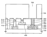
100: 반도체 기판, 210: 게이트 구조,100: semiconductor substrate, 210: gate structure,
300: 제1절연층, 305, 505: 매몰 콘택,300: first insulating layer, 305, 505: investment contact,
400: 비트 라인, 500: 제2절연층,400: bit line, 500: second insulating layer,
511, 513, 515: 제1, 제2 및 제3하부 콘택홀,511, 513, and 515: first, second and third lower contact holes,
600: 식각 종료층, 700: 제3절연층,600: etching termination layer, 700: third insulating layer,
710: 보이드, 810: 하부 전극,710: void, 810: lower electrode,
830: 유전층, 850: 상부 전극,830: dielectric layer, 850: top electrode,
900: 제4절연층, 900: fourth insulating layer,
911, 913, 915: 제1, 제2 및 제3상부 콘택홀,911, 913, and 915: first, second and third upper contact holes,
917: 제4금속 콘택홀, 1000: 금속 콘택층.917: fourth metal contact hole, 1000: metal contact layer.
본 발명은 반도체 소자 제조 방법에 관한 것으로, 특히, 커패시터 및 금속 콘택(metal contact)을 제조하는 방법에 관한 것이다. TECHNICAL FIELD The present invention relates to a method of manufacturing a semiconductor device, and more particularly, to a method of manufacturing a capacitor and a metal contact.
반도체 소자가 고집적화됨에 따라 피치 크기(pitch size)가 작아져서 사진 공정 및 식각 공정의 마진(margin)이 점차 감소하고 있다. 상세하게는 단차가 20000Å 이상의 절연층을 선택적으로 패터닝하여 금속 콘택을 형성하는 DSMC(Deep and Small Metal Contact) 공정을 적용할 경우, 사진 공정뿐만 아니라 식각 공정에서도 많은 어려움이 도출되고 있다. 이러한 DSMC 공정은 COB(Capacitor On Bit line) 구조 또는 다층 배선 구조에서 다수 채용되고 있으므로, 상기한 바와 같은 어려움을 극복하는 것이 요구되고 있다. As semiconductor devices are highly integrated, the margins of the photolithography and etching processes are gradually reduced due to the smaller pitch size. In detail, when the DSMC (Deep and Small Metal Contact) process of selectively patterning an insulating layer having a step of 20000 Å or more to form a metal contact is applied, many difficulties are induced not only in the photo process but also in the etching process. Since many DSMC processes are employed in a COB (Capacitor On Bit line) structure or a multi-layer wiring structure, it is required to overcome the above-mentioned difficulties.
이에 따라, 이러한 금속 콘택은 실질적으로 2단계에 걸쳐 이루어지고 있다. 상세하게 설명하면, 비트 라인 상부에 제1절연층을 형성하여 단차(또는 두께가 10000Å) 정도일 때 금속 콘택 공정, 예컨대, 제1콘택홀 형성 및 제1금속층 증착 등을 포함하는 제1금속 콘택 공정을 수행하여, 금속 플러그(metal plug) 또는 금속 스터드(metal stud)를 형성한다. 이때, 금속층은 일반적으로 텅스텐과 같은 금속 물질로 이루어질 수 있다. Accordingly, such metal contact is substantially made in two steps. In detail, a first metal contact process including a metal contact process, for example, forming a first contact hole and depositing a first metal layer when the first insulating layer is formed on the bit line and has a step (or a thickness of about 10000 μs), is described. To form a metal plug or a metal stud. In this case, the metal layer may generally be made of a metal material such as tungsten.
이후에, 후속 공정으로 이러한 금속 플러그 또는 금속 스터드 상에 제2금속 콘택 공정, 예컨대, 제1절연층 상에 제2절연층을 형성하고 금속 플러그 또는 금속 스터드를 노출하는 제2콘택홀 형성 및 제2금속층 증착 등을 포함하는 제2금속 콘택 공정을 수행하여 금속 플러그 또는 금속 스터드에 연결되는 금속 배선층을 형성한다. 이때, 상기한 바와 같은 제1금속 콘택 공정 및 제2금속 콘택 공정 사이에 커패시터 공정이 더 수행된다. Subsequently, a second metal contact process is formed on the metal plug or metal stud in a subsequent process, for example, a second contact hole is formed on the first insulating layer and the second contact hole is formed to expose the metal plug or metal stud. A second metal contact process including a second metal layer deposition or the like is performed to form a metal wiring layer connected to the metal plug or the metal stud. At this time, a capacitor process is further performed between the first metal contact process and the second metal contact process as described above.
이와 같은 금속 콘택 및 커패시터를 제조하는 공정은 전체적으로 공정이 복잡하여 생산성이 떨어질 수 있다. The process of manufacturing such metal contacts and capacitors may be complicated and the productivity may be reduced.
본 발명이 이루고자 하는 기술적 과제는, 단차를 극복하여 전체 공정을 단순화할 수 있는 금속 콘택 및 커패시터를 포함하는 반도체 소자 제조 방법을 제공하는 데 있다. SUMMARY OF THE INVENTION The present invention has been made in an effort to provide a method for manufacturing a semiconductor device including a metal contact and a capacitor capable of simplifying an entire process by overcoming a step.
상기의 기술적 과제를 달성하기 위한 본 발명의 일 관점은, 반도체 기판 상에 게이트 구조를 형성하고 상기 게이트 구조를 덮는 제1절연층을 형성한다. 상기 제1절연층 상에 비트 라인을 형성하고, 상기 비트 라인을 덮는 제2절연층을 형성한다. 상기 제2절연층을 관통하여 상기 게이트 구조들 간의 상기 반도체 기판에 전기적으로 연결되는 매몰 콘택을 형성하고, 상기 제2절연층을 선택적으로 식각하여 상기 반도체 기판, 상기 비트 라인 및 상기 게이트 구조의 도전 패턴을 각각 노출하는 하부 콘택홀들을 형성한다. 상기 제2절연층 상에 상기 하부 콘택홀들의 내부에 보이드를 유발하는 제3절연층을 형성한다. 상기 제3절연층을 패터닝하고 패터닝된 상기 제3절연층을 몰드로 이용하여 상기 매몰 콘택에 전기적으로 연결되는 커패시 터의 하부 전극을 형성하고 상기 하부 전극 상에 유전층 및 상부 전극을 형성하여 커패시터를 형성한다. 상기 커패시터를 덮는 제4절연층을 형성한 후 상기 제4절연층 및 하부의 절연층들을 순차적으로 선택적으로 식각하여 상기 하부 콘택홀들 각각에 정렬되도록 형성되는 상부 콘택홀들로 이루어지거나 상기 상부 전극을 노출하는 금속 콘택홀들을 형성한다. 상기 금속 콘택홀 및 상기 상부 콘택홀들 및 상기 상부 콘택홀들에 정렬된 상기 하부 콘택홀들을 모두 채워 상기 상부 전극, 상기 반도체 기판, 상기 비트 라인 및 상기 도전 패턴 각각에 전기적으로 연결되는 금속 콘택을 형성한다. An aspect of the present invention for achieving the above technical problem, to form a gate structure on a semiconductor substrate and to form a first insulating layer covering the gate structure. A bit line is formed on the first insulating layer, and a second insulating layer covering the bit line is formed. Forming a buried contact electrically connected to the semiconductor substrate between the gate structures through the second insulating layer, and selectively etching the second insulating layer to electrically conductive the semiconductor substrate, the bit line, and the gate structure. Lower contact holes respectively exposing the pattern are formed. A third insulating layer is formed on the second insulating layer to cause voids in the lower contact holes. Patterning the third insulating layer and forming a lower electrode of a capacitor electrically connected to the buried contact using the patterned third insulating layer as a mold, and forming a dielectric layer and an upper electrode on the lower electrode To form. After the fourth insulating layer covering the capacitor is formed, the fourth insulating layer and the lower insulating layers may be selectively etched sequentially to form the upper contact holes formed to be aligned with each of the lower contact holes, or the upper electrode. Form metal contact holes exposing the metal. The metal contact hole and the lower contact holes aligned with the upper contact holes and the upper contact holes are filled to fill the metal contact electrically connected to the upper electrode, the semiconductor substrate, the bit line, and the conductive pattern, respectively. Form.
상기 제3절연층은 플라즈마 강화 화학 기상 증착법에 의한 절연층을 포함한다. 상기 하부 콘택홀들은 상기 상부 콘택홀들에 비해 작은 선폭으로 형성될 수 있다. The third insulating layer includes an insulating layer by plasma enhanced chemical vapor deposition. The lower contact holes may be formed to have a smaller line width than the upper contact holes.
상술한 본 발명에 따르면, 금속 플러그 또는 금속 스터드 등을 형성하는 공정 단계를 생략할 수 있어, 전체 공정을 보다 간략화 또는 단순화할 수 있다. According to the present invention described above, the step of forming a metal plug or a metal stud and the like can be omitted, so that the entire process can be simplified or simplified.
이하, 첨부 도면을 참조하여 본 발명의 실시예를 상세히 설명한다. 그러나, 본 발명의 실시예들은 여러 가지 다른 형태로 변형될 수 있으며, 본 발명의 범위가 아래에서 상술하는 실시예들로 인해 한정되어지는 것으로 해석되어져서는 안된다. 본 발명의 실시예들은 당업계에서 평균적인 지식을 가진 자에게 본 발명을 보다 완전하게 설명하기 위해서 제공되어지는 것이다. 따라서, 도면에서의 요소의 형상 등은 보다 명확한 설명을 강조하기 위해서 과장되어진 것이며, 도면 상에서 동일한 부호로 표시된 요소는 동일한 요소를 의미한다. 또한, 어떤 층이 다른 층 또는 반 도체 기판의 "상"에 있다라고 기재되는 경우에, 상기 어떤 층은 상기 다른 층 또는 반도체 기판에 직접 접촉하여 존재할 수 있고, 또는, 그 사이에 제3의 층이 개재되어질 수 있다.Hereinafter, embodiments of the present invention will be described in detail with reference to the accompanying drawings. However, embodiments of the present invention may be modified in many different forms, and the scope of the present invention should not be construed as being limited by the embodiments described below. Embodiments of the present invention are provided to more completely explain the present invention to those skilled in the art. Accordingly, the shape and the like of the elements in the drawings are exaggerated to emphasize a more clear description, and the elements denoted by the same reference numerals in the drawings means the same elements. In addition, when a layer is described as being "on" another layer or semiconductor substrate, the layer may be in direct contact with the other layer or semiconductor substrate, or a third layer therebetween. This may be intervened.
도 1 내지 도 7은 본 발명의 제1실시예에 의한 금속 콘택 및 커패시터를 포함하는 반도체 소자 제조 방법을 설명하기 위해서 개략적으로 도시한 단면도들이다. 1 to 7 are cross-sectional views schematically illustrating a method of manufacturing a semiconductor device including a metal contact and a capacitor according to a first embodiment of the present invention.
도 1은 반도체 기판(100) 상에 매몰 콘택(buried contact:305, 505)을 형성하는 단계를 개략적으로 나타낸다. FIG. 1 schematically illustrates forming
구체적으로, 반도체 기판(100)상에 다층의 도전 패턴 및 이러한 도전 패턴을 둘러싸 보호하는 절연 물질의 보호층 등으로 이루어지는 게이트 구조(210)를 형성한 후, 게이트 구조(210)를 덮는 제1절연층(300)을 형성한다. Specifically, after forming a
이후에, 제1절연층(300) 상에 사진 식각 공정을 수행하여 게이트 구조(210) 간의 반도체 기판(100)을 노출하는 제1매몰 콘택홀을 형성한 후, 제1매몰 콘택홀을 채우는 제1매몰 콘택(305)을 형성한다. 이때, 제1매몰 콘택홀은 알려진 SAC(Self Aligned Contact) 공정을 따라 형성될 수 있다. 이후에, 제1절연층(300) 상에 도전 물질로 이루어지고 하부에 장벽층을 수반하는 비트 라인(bit line:400)을 형성하고, 비트 라인(400)을 덮는 제2절연층(500)을 형성한다. Thereafter, a first etching contact hole exposing the
제2절연층(500) 상에 사진 식각 공정을 수행하여 제1매몰 콘택(305)을 노출하는 제2매몰 콘택홀(501)을 형성한 후, 이러한 제2매몰 콘택홀(501)을 메우는 제2매몰 콘택(505)을 형성한다. 이에 따라, 제1 및 제2매몰 콘택(305, 505)으로 이루 어지는 매몰 콘택(305, 505) 구조가 이루어진다. 이러한 매몰 콘택(305, 505)은 텅스텐 또는 도전성 폴리 실리콘(poly silicon) 등으로 이루어질 수 있으며, 제1절연층(300) 및 제2절연층(500)은 실리콘 산화물 등과 같은 절연 물질로 이루어질 수 있다. 또한, 제1절연층(300) 및 제2절연층(500) 등은 대략 10000Å 정도의 단차(또는 두께)로 형성될 수 있다. After forming the second buried
상기한 제2절연층(500)을 형성한 후 제2절연층(500) 상에 식각 종료층(600)을 형성할 수 있다. 이러한 식각 종료층(600)은 후속 공정에서 식각 종료의 작용을 하며, 후속에 증착될 절연 물질과 다른 식각율을 가지는 절연 물질, 예컨대, 실리콘 질화물 등으로 이루어질 수 있다. After forming the second
한편, 상기 제1매몰 콘택홀 및 제2매몰 콘택홀(501)은 각각 매몰 콘택(305, 505)을 위한 콘택홀을 의미하는 것으로 본 발명의 실시예들에서 기술된다. Meanwhile, the first buried contact hole and the second buried
도 2는 제2 및 제1절연층(500, 300)을 순차적으로 식각하여 제1, 제2 및 제3하부 콘택홀(511, 513, 515)을 형성하는 단계를 개략적으로 나타낸다. 2 schematically illustrates the steps of sequentially etching the second and first
구체적으로, 사진 식각 공정을 이용하여 제2절연층(500) 및 제1절연층(300)을 순차적으로 식각하여 제1, 제2 및 제3하부 콘택홀(511, 513, 515)을 형성한다. 이때, 제2절연층(500) 상에 존재하는 식각 종료층(600) 또한 상기 식각 공정에 의해서 패터닝될 수 있다. In detail, the first
이때, 상기한 제1하부 콘택홀(511)은 제2절연층(500) 하부의 비트 라인(400)을 노출하도록 설정되며, 제2하부 콘택홀(513)은 게이트 구조(210)의 도전 패턴의 상측 표면을 노출하도록 설정되고, 제3하부 콘택홀(515)은 반도체 기판(100)의 활 성 영역(active region)을 노출하도록 각각 설정될 수 있다. 이러한 제1, 제2 및 제3하부 콘택홀(511, 513, 515)은 금속 콘택을 위해서 준비된다. In this case, the first
그리고, 이후의 금속 콘택에서 오믹 콘택(ohmic contact)을 구현하도록 제1, 제2 및 제3하부 콘택홀(511, 513, 515)을 형성한 후 오믹층(도시되지 않음)을 형성하는 단계를 더 수행할 수 있다. After the first, second and third lower contact holes 511, 513, and 515 are formed to realize ohmic contact in the subsequent metal contact, an ohmic layer (not shown) may be formed. More can be done.
도 3은 제2절연층(500) 상에 제3절연층(700)을 형성하는 단계를 개략적으로 나타낸다. 3 schematically illustrates a step of forming a third
구체적으로, 제2절연층(500), 실질적으로는 식각 종료층(600) 상에 제3절연층(700)을 형성한다. 이때, 제3절연층(700)은 단차 도포성(step coverage)이 열악한 절연 물질층으로 형성하여, 제1, 제2 및 제3하부 콘택홀(511, 513, 515)에 보이드(void:710)를 유발하도록 형성한다. 본 발명의 실시예에서 이러한 보이드의 정도가 극심할수록 바람직하다. 이러한 단차 도포성이 열악한 절연 물질층으로는 단차 도포성이 열악한 CVD-산화물층(Chemical Vapor Deposition-oxide layer), 예컨대, 플라즈마 강화(plasma enhanced)-CVD 절연층을 예로 들 수 있다. In detail, the third insulating
상기한 바와 같이 제3절연층(700)을 형성한 후, 사진 식각 공정을 이용하여 매몰 콘택(305, 505)을 노출하는 오픈닝(opening:705)을 형성한다. 이러한 오픈닝(705)은 상기한 제3절연층(700)이 후속에 형성되는 커패시터의 하부 전극에 컨케이브(concave) 형태의 형상을 부여하는 몰드(mold)로 이용되도록 하기 위해서 형성된다. After the third insulating
이와 같이 제3절연층(700)은 커패시터의 하부 전극의 형상을 부여하기 위한 몰드로 이용되므로, 그 두께는 커패시터의 높이에 따라 달라질 수 있다. 즉, 하부 전극의 높이에 따라 제3절연층(700)의 높이가 설정된다. 본 발명의 제1실시예에서는 대략 10000Å 정도의 두께로 제3절연층(700)이 형성될 수 있다. As such, since the third insulating
도 4는 매몰 콘택(305, 505)에 연결되는 커패시터의 하부 전극(810)을 형성하는 단계를 개략적으로 나타낸다. 4 schematically illustrates forming a
구체적으로, 오픈닝(705)에 의해서 노출되는 매몰 콘택(305, 505)에 연결되는 하부 전극층을 도전 물질, 예컨대, 도전성 폴리 실리콘층으로 형성한 후, 에치 백(etch back) 또는 CMP(Chemical Mechanical Polishing) 등으로 패터닝하여 컨케이브 형태의 하부 전극(810)을 형성한다. 이러한 하부 전극(810)은 커패시터를 이루기 위해서 형성되므로, 일반적인 커패시터의 전극 물질로 형성될 수 있다.Specifically, the lower electrode layer connected to the buried
도 5는 하부 전극(810) 상에 유전층(830) 및 상부 전극(850)을 형성하는 단계를 개략적으로 나타낸다. 5 schematically illustrates forming a
구체적으로, 하부 전극(810) 상에 유전층(830) 및 상부 전극(850)을 형성하여 커패시터를 구성한다. 유전층(830) 및 상부 전극(850)은 일반적인 커패시터에 이용되는 유전 물질 및 전극 물질로 각각 형성될 수 있다. Specifically, a capacitor is formed by forming the
도 6은 상부 전극(850) 상의 제4절연층(900)에 제1, 제2 및 제3상부 콘택홀(911, 913, 915) 및 제4금속 콘택홀(917)을 형성하는 단계를 개략적으로 나타낸다. FIG. 6 schematically illustrates forming first, second and third upper contact holes 911, 913, and 915 and a fourth
구체적으로, 상부 전극(850)이 완성된 커패시터를 절연하는 제4절연층(900)을 형성한다. 이후에, 제4절연층(900)을 사진 식각 공정으로 패터닝하여 제1하부 콘택홀(511)에 연결되는 제1상부 콘택홀(911), 제2하부 콘택홀(513)에 연결되는 제1상부 콘택홀(913) 및 제3하부 콘택홀(515)에 연결되는 제3상부 콘택홀(915)을 형성한다. In detail, the fourth insulating
이때, 제1, 제2 및 제3상부 콘택홀(911, 913, 915)은 각각 제1, 제2 및 제3하부 콘택홀(511, 513, 515) 보다 넓은 크기로 형성되는 것이 바람직하다. 이는 오정렬(misalign)이 발생하는 것을 방지하고, 제1, 제2 및 제3하부 콘택홀(511, 513, 515)들의 내부에 보이드(710)가 유발되는 것을 보다 효과적으로 유도하기 위해서이다.In this case, the first, second, and third upper contact holes 911, 913, and 915 may be formed to have a larger size than the first, second, and third lower contact holes 511, 513, and 515, respectively. This is to prevent misalignment from occurring and to more effectively induce the occurrence of the void 710 in the first, second and third lower contact holes 511, 513, and 515.
한편, 제1, 제2 및 제3상부 콘택홀(911, 913, 915)과 함께, 상부 전극(850)의 표면을 노출하는 제4금속 콘택홀(917)을 형성한다. The fourth
이때, 제1, 제2 및 제3하부 콘택홀(511, 513, 515) 내에는 보이드(710)가 유발되어 있으므로, 식각 공정은 실질적으로 제1, 제2 및 제3상부 콘택홀(911, 913, 915)을 위한 제4절연층(900) 및 제3절연층(700)을 식각하는 것과 대등한 정도로 수행될 수 있다. 즉, 제1, 제2 및 제3하부 콘택홀(511, 513, 515) 내에는 보이드(710)가 존재하므로, 이러한 보이드(710)가 노출될 때까지 식각 공정을 수행하면, 반도체 기판(100), 게이트 구조(210)의 도전 패턴 또는 비트 라인(400)을 모두 노출할 수 있다. In this case, since the
따라서, 반도체 기판(100), 게이트 구조(210)의 도전 패턴 또는 비트 라인(400)을 모두 노출하기 위해서, 제1, 제2, 제3 및 제4절연층(300, 500, 700, 900)을 한번에 식각할 필요가 없다. 만일, 단 한 차례의 식각 공정으로 제1, 제2, 제3 및 제4절연층(300, 500, 700, 900)을 식각하여 반도체 기판(100), 게이트 구조(210)의 도전 패턴 또는 비트 라인(400)을 모두 노출할 경우, 제4금속 콘택홀(917)에 의해서 노출되는 상부 전극(850)이 극심하게 식각되어 손상되는 것을 회피할 수 없게 된다. Accordingly, the first, second, third, and fourth insulating
그러나, 본 발명의 실시예에서는 하부에 유발된 보이드(710)의 존재에 의해서 제4금속 콘택홀(917)을 형성하는 식각 공정이, 실질적으로, 제3절연층(700) 및 제4절연층(900)의 두께 정도만 식각하도록 수행되므로, 상부 전극(850)이 손상되는 것을 최소화할 수 있다. 또한, 보이드(710)의 존재에 의해서 식각 공정을 수행할 때 단차를 용이하게 극복할 수 있다. 더욱이, 보이드(710)의 존재에 의해서 제1, 제2 및 제3상부 콘택홀(911, 913, 915)을 형성하는 식각 공정은 노출되는 반도체 기판(100)의 활성 영역을 과다하게 식각하는 것이 배제되므로, 반도체 기판(100)의 활성 영역이 손상되는 것을 방지할 수 있다. However, in the exemplary embodiment of the present invention, the etching process of forming the fourth
상술한 바에 따라, 제1, 제2 및 제3상부 콘택홀(911, 913, 915)과 이에 각각에 연결되는 제1, 제2 및 제3하부 콘택홀(511, 513, 515)과 제4금속 콘택홀(917)과 같은 금속 콘택홀들이 형성된다. As described above, the first, second and third upper contact holes 911, 913, and 915, and the first, second and third lower contact holes 511, 513, 515 and fourth connected thereto, respectively, Metal contact holes such as the
도 7은 금속 콘택층(1000)을 형성하는 단계를 개략적으로 나타낸다. 7 schematically illustrates forming a
구체적으로, 제4절연층(900) 상에 제1, 제2 및 제3상부 콘택홀(911, 913, 915) 및 제4금속 콘택홀(917)을 메우는 금속 콘택층(1000)을 형성한다. 이러한 금속 콘택층(1000)은 제1, 제2 및 제3상부 콘택홀(911, 913, 915) 각각의 하부에 존재하는 제1, 제2 및 제3하부 콘택홀(511, 513, 515)을 채워 각각 반도체 기판(100), 게이트 구조(210)의 도전 패턴 및 비트 라인(400)에 전기적으로 연결되도록 함으로써 금속 콘택을 형성한다.Specifically, the
이때, 금속 콘택에서 오믹 콘택(ohmic contact)을 구현하도록 제1, 제2 및 제3하부 콘택홀(511, 513, 515)을 형성한 후 오믹층(도시되지 않음)을 형성하는 단계를 더 수행할 수 있다. 또는 제1, 제2 및 제3상부 콘택홀(911, 913, 915) 및 제4금속 콘택홀(917)을 형성한 후, 오믹층(도시되지 않음)을 형성하는 단계를 더 수행할 수 있다. In this case, after the first, second and third lower contact holes 511, 513, and 515 are formed to realize ohmic contact in the metal contact, an ohmic layer (not shown) is further performed. can do. Alternatively, after forming the first, second and third upper contact holes 911, 913, and 915 and the fourth
이때, 금속 콘택층(1000)은 텅스텐 또는 구리, 알루미늄 등과 같은 도전 물질로 형성될 수 있으며, 단차 도포성이 우수한 증착 방법, 예컨대, CVD, ALD(Atomic Layered Deposition) 또는 전기 도금법(electroplating) 등으로 금속 콘택층(1000)은 형성될 수 있다. 예를 들어, 텅스텐층으로 금속 콘택층(1000)이 이루어질 때는 CVD 방법을 이용하여 높은 단차 도포성을 구현할 수 있고, 알루미늄의 경우 ALD 방법에 의해서 높은 단차 도포성을 구현할 수 있으며, 구리층의 경우 전기 도금법을 이용할 수 있다. In this case, the
이후에, 금속 콘택층(1000)을 배선의 역할을 하도록 패터닝하는 공정을 수행할 수 있다. Thereafter, a process of patterning the
상기한 바와 같은 본 발명의 실시예에서는 종래와는 달리 금속 플러그 또는 금속 스터드 등을 형성하는 중간 단계가 생략될 수 있어, 전체 공정을 보다 간략화 또는 단순화할 수 있다. Unlike the conventional embodiment of the present invention as described above, an intermediate step of forming a metal plug or a metal stud may be omitted, thereby simplifying or simplifying the entire process.
도 8 내지 도 10은 본 발명의 제2실시예에 의한 금속 콘택 및 커패시터를 포 함하는 반도체 소자 제조 방법을 설명하기 위해서 개략적으로 도시한 단면도들이다. 8 to 10 are cross-sectional views schematically illustrating a method of manufacturing a semiconductor device including a metal contact and a capacitor according to a second embodiment of the present invention.
제2실시예에서는 제1실시예에서와 달리 커패시터의 유전층(830') 및 상부 전극(850')을 형성하는 단계 및 이에 연관된 공정에서 차이가 있다. 그러나, 커패시터 공정 이전의 공정은 대등하며, 제2실시예에서 인용되는 제1실시예에서와 동일한 참조 부호는 동일한 부재를 의미한다. In the second embodiment, unlike in the first embodiment, there is a difference in the steps of forming the dielectric layer 830 'and the upper electrode 850' of the capacitor and the process associated therewith. However, the process before the capacitor process is equivalent, and the same reference numerals as in the first embodiment referred to in the second embodiment mean the same members.
구체적으로, 제1실시예에서 도 1 내지 도 4를 참조하여 설명한 바와 같이 제3절연층(700)을 형성한 후, 오프닝(705)을 이용하여 커패시터의 하부 전극(810)을 형성한다. Specifically, after the third insulating
도 8은 몰드로 이용된 제3절연층(700)을 제거하는 단계를 개략적으로 나타낸다. 8 schematically shows a step of removing the third insulating
구체적으로, 하부 전극(810)을 형성한 후에 몰드로 이용된 제3절연층(700)을 선택적으로 제거한다. 이때, 선택적인 습식 식각을 이용할 수 있으며, 이러한 식각 공정은 하부의 식각 종료층(600)에서 종료될 수 있다. 이에 따라, 하부의 제1, 제2 및 제3하부 콘택홀(511, 513, 515)의 상측 입구 부분에는 상기한 제3절연층(700)의 일부가 잔류할 수 있어 하부의 제1, 제2 및 제3하부 콘택홀(511, 513, 515)의 내부 보이드(710)가 식각 공정에 노출되는 것이 방지될 수 있다. Specifically, after the
이와 같이 제3절연층(700)이 제거됨으로써 하부 전극(810)의 외측 표면이 노출될 수 있다. As such, the outer surface of the
도 9는 하부 전극(810) 상에 유전층(830') 및 상부 전극(850')을 형성하고 제4절연층(900')을 형성하는 단계를 개략적으로 나타낸다. FIG. 9 schematically illustrates forming a dielectric layer 830 'and an upper electrode 850' on the
구체적으로, 하부 전극(810) 상에 유전층(830') 및 상부 전극(850')을 증착 및 패터닝 공정을 통해서 형성한다. 제1실시예에서와는 달리 하부 전극(810)의 외측 표면 상에도 유전층(830')이 덮고 있으므로, 구성되는 커패시터의 정전 용량을 보다 더 확보할 수 있다. 이후에, 상부 전극(850')을 덮는 제4절연층(900')을 형성한다. In detail, the dielectric layer 830 'and the upper electrode 850' are formed on the
도 10은 제4절연층(900')을 패터닝하여 제1, 제2 및 제3상부 콘택홀(911', 913', 915') 및 제4금속 콘택홀(917')을 형성하고 금속 콘택층(1000')을 형성하는 단계를 개략적으로 나타낸다. FIG. 10 illustrates the fourth insulating
구체적으로, 제4절연층(900')을 사진 식각 공정으로 선택적으로 식각하여 제1, 제2 및 제3하부 콘택홀(511, 513, 515)에 각각 정렬되어 연결되는 제1, 제2 및 제3상부 콘택홀(911', 913', 915')을 형성한다. 이때, 잔류된 제3절연층(700) 또한 제거된다. 이와 함께 상부 전극(850')의 일부를 노출하는 제4금속 콘택홀(917') 또한 형성된다. In detail, the fourth insulating
이후에, 제1, 제2 및 제3하부 콘택홀(511, 513, 515) 및 이에 각각 정렬된 제1, 제2 및 제3상부 콘택홀(911', 913', 915'), 그리고, 제4금속 콘택홀(917')과 같은 금속 콘택홀을 채우는 금속 콘택층(1000')을 형성한다. 금속 콘택층(1000')은 텅스텐 또는 구리, 알루미늄 등과 같은 도전 물질로 형성될 수 있으며, 단차 도포성이 우수한 증착 방법, 예컨대, CVD, ALD 또는 전기 도금법 등의 방법으로 형성될 수 있다. 이후에, 필요에 따라 금속 콘택층(1000')을 패터닝하여 배선으로 이용할 수 있다. Thereafter, the first, second and third lower contact holes 511, 513, and 515 and the first, second and third upper contact holes 911 ′, 913 ′, and 915 ′ aligned therewith, respectively, The
이상, 본 발명을 구체적인 실시예를 통하여 상세히 설명하였으나, 본 발명은 이에 한정되지 않고, 본 발명의 기술적 사상 내에서 당 분야의 통상의 지식을 가진 자에 의해 그 변형이나 개량이 가능함이 명백하다. As mentioned above, although this invention was demonstrated in detail through the specific Example, this invention is not limited to this, It is clear that the deformation | transformation and improvement are possible by the person of ordinary skill in the art within the technical idea of this invention.
상술한 본 발명에 따르면, 커패시터에 의한 절연층의 높은 단차를 극복하여 금속 콘택홀을 형성할 수 있으며, 금속 플러그 또는 금속 스터드 등을 형성하는 공정 단계를 생략할 수 있어, 전체 공정을 보다 간략화 또는 단순화할 수 있다. According to the present invention described above, the metal contact hole can be formed by overcoming the high step of the insulating layer by the capacitor, and the process step of forming the metal plug or the metal stud can be omitted, thereby simplifying the entire process or Can be simplified.
Claims (4)
Priority Applications (2)
| Application Number | Priority Date | Filing Date | Title |
|---|---|---|---|
| KR1020000046090A KR100630666B1 (en) | 2000-08-09 | 2000-08-09 | Method for manufacturing semiconductor device including metal contact and capacitor |
| US09/923,437 US6534361B2 (en) | 2000-08-09 | 2001-08-08 | Method of manufacturing a semiconductor device including metal contact and capacitor |
Applications Claiming Priority (1)
| Application Number | Priority Date | Filing Date | Title |
|---|---|---|---|
| KR1020000046090A KR100630666B1 (en) | 2000-08-09 | 2000-08-09 | Method for manufacturing semiconductor device including metal contact and capacitor |
Publications (2)
| Publication Number | Publication Date |
|---|---|
| KR20020012857A KR20020012857A (en) | 2002-02-20 |
| KR100630666B1 true KR100630666B1 (en) | 2006-10-02 |
Family
ID=19682432
Family Applications (1)
| Application Number | Title | Priority Date | Filing Date |
|---|---|---|---|
| KR1020000046090A Expired - Fee Related KR100630666B1 (en) | 2000-08-09 | 2000-08-09 | Method for manufacturing semiconductor device including metal contact and capacitor |
Country Status (2)
| Country | Link |
|---|---|
| US (1) | US6534361B2 (en) |
| KR (1) | KR100630666B1 (en) |
Families Citing this family (44)
| Publication number | Priority date | Publication date | Assignee | Title |
|---|---|---|---|---|
| US6974766B1 (en) * | 1998-10-01 | 2005-12-13 | Applied Materials, Inc. | In situ deposition of a low κ dielectric layer, barrier layer, etch stop, and anti-reflective coating for damascene application |
| US6620723B1 (en) | 2000-06-27 | 2003-09-16 | Applied Materials, Inc. | Formation of boride barrier layers using chemisorption techniques |
| US7405158B2 (en) | 2000-06-28 | 2008-07-29 | Applied Materials, Inc. | Methods for depositing tungsten layers employing atomic layer deposition techniques |
| US7964505B2 (en) | 2005-01-19 | 2011-06-21 | Applied Materials, Inc. | Atomic layer deposition of tungsten materials |
| US7101795B1 (en) * | 2000-06-28 | 2006-09-05 | Applied Materials, Inc. | Method and apparatus for depositing refractory metal layers employing sequential deposition techniques to form a nucleation layer |
| US7732327B2 (en) | 2000-06-28 | 2010-06-08 | Applied Materials, Inc. | Vapor deposition of tungsten materials |
| US6936538B2 (en) | 2001-07-16 | 2005-08-30 | Applied Materials, Inc. | Method and apparatus for depositing tungsten after surface treatment to improve film characteristics |
| US6551929B1 (en) | 2000-06-28 | 2003-04-22 | Applied Materials, Inc. | Bifurcated deposition process for depositing refractory metal layers employing atomic layer deposition and chemical vapor deposition techniques |
| US6849545B2 (en) * | 2001-06-20 | 2005-02-01 | Applied Materials, Inc. | System and method to form a composite film stack utilizing sequential deposition techniques |
| US7211144B2 (en) | 2001-07-13 | 2007-05-01 | Applied Materials, Inc. | Pulsed nucleation deposition of tungsten layers |
| US20070009658A1 (en) * | 2001-07-13 | 2007-01-11 | Yoo Jong H | Pulse nucleation enhanced nucleation technique for improved step coverage and better gap fill for WCVD process |
| TW581822B (en) * | 2001-07-16 | 2004-04-01 | Applied Materials Inc | Formation of composite tungsten films |
| WO2003030224A2 (en) | 2001-07-25 | 2003-04-10 | Applied Materials, Inc. | Barrier formation using novel sputter-deposition method |
| US20030029715A1 (en) | 2001-07-25 | 2003-02-13 | Applied Materials, Inc. | An Apparatus For Annealing Substrates In Physical Vapor Deposition Systems |
| US20090004850A1 (en) | 2001-07-25 | 2009-01-01 | Seshadri Ganguli | Process for forming cobalt and cobalt silicide materials in tungsten contact applications |
| US9051641B2 (en) | 2001-07-25 | 2015-06-09 | Applied Materials, Inc. | Cobalt deposition on barrier surfaces |
| US8110489B2 (en) | 2001-07-25 | 2012-02-07 | Applied Materials, Inc. | Process for forming cobalt-containing materials |
| US7049226B2 (en) | 2001-09-26 | 2006-05-23 | Applied Materials, Inc. | Integration of ALD tantalum nitride for copper metallization |
| US6936906B2 (en) | 2001-09-26 | 2005-08-30 | Applied Materials, Inc. | Integration of barrier layer and seed layer |
| TW589684B (en) * | 2001-10-10 | 2004-06-01 | Applied Materials Inc | Method for depositing refractory metal layers employing sequential deposition techniques |
| US6916398B2 (en) | 2001-10-26 | 2005-07-12 | Applied Materials, Inc. | Gas delivery apparatus and method for atomic layer deposition |
| US7780785B2 (en) | 2001-10-26 | 2010-08-24 | Applied Materials, Inc. | Gas delivery apparatus for atomic layer deposition |
| US6809026B2 (en) * | 2001-12-21 | 2004-10-26 | Applied Materials, Inc. | Selective deposition of a barrier layer on a metal film |
| US6998014B2 (en) | 2002-01-26 | 2006-02-14 | Applied Materials, Inc. | Apparatus and method for plasma assisted deposition |
| US6911391B2 (en) | 2002-01-26 | 2005-06-28 | Applied Materials, Inc. | Integration of titanium and titanium nitride layers |
| US6827978B2 (en) * | 2002-02-11 | 2004-12-07 | Applied Materials, Inc. | Deposition of tungsten films |
| US6833161B2 (en) | 2002-02-26 | 2004-12-21 | Applied Materials, Inc. | Cyclical deposition of tungsten nitride for metal oxide gate electrode |
| US6720027B2 (en) * | 2002-04-08 | 2004-04-13 | Applied Materials, Inc. | Cyclical deposition of a variable content titanium silicon nitride layer |
| US6846516B2 (en) * | 2002-04-08 | 2005-01-25 | Applied Materials, Inc. | Multiple precursor cyclical deposition system |
| US7279432B2 (en) | 2002-04-16 | 2007-10-09 | Applied Materials, Inc. | System and method for forming an integrated barrier layer |
| US6838125B2 (en) * | 2002-07-10 | 2005-01-04 | Applied Materials, Inc. | Method of film deposition using activated precursor gases |
| US6821563B2 (en) | 2002-10-02 | 2004-11-23 | Applied Materials, Inc. | Gas distribution system for cyclical layer deposition |
| US7262133B2 (en) * | 2003-01-07 | 2007-08-28 | Applied Materials, Inc. | Enhancement of copper line reliability using thin ALD tan film to cap the copper line |
| KR20060079144A (en) * | 2003-06-18 | 2006-07-05 | 어플라이드 머티어리얼스, 인코포레이티드 | Atomic Layer Deposition of Barrier Materials |
| TWI237871B (en) * | 2003-11-17 | 2005-08-11 | Nanya Technology Corp | Method of forming contacts for memory device |
| US7429402B2 (en) * | 2004-12-10 | 2008-09-30 | Applied Materials, Inc. | Ruthenium as an underlayer for tungsten film deposition |
| US20070099422A1 (en) * | 2005-10-28 | 2007-05-03 | Kapila Wijekoon | Process for electroless copper deposition |
| US7850779B2 (en) | 2005-11-04 | 2010-12-14 | Applied Materisals, Inc. | Apparatus and process for plasma-enhanced atomic layer deposition |
| KR100742281B1 (en) * | 2006-01-23 | 2007-07-24 | 삼성전자주식회사 | Semiconductor device and manufacturing method thereof |
| US7772064B2 (en) * | 2007-03-05 | 2010-08-10 | United Microelectronics Corp. | Method of fabricating self-aligned contact |
| US20160138166A1 (en) * | 2014-11-19 | 2016-05-19 | Lam Research Corporation | Systems and methods for forming selective metal electrode layers for resistive switching memories |
| TW201700761A (en) | 2015-05-13 | 2017-01-01 | 應用材料股份有限公司 | A tungsten film modified by pretreatment of an organic metal or germane through a substrate |
| US20200411635A1 (en) * | 2019-06-28 | 2020-12-31 | Intel Corporation | Air gaps and capacitors in dielectric layers |
| CN112820828B (en) * | 2019-11-15 | 2023-08-04 | 夏泰鑫半导体(青岛)有限公司 | Semiconductor device and method for manufacturing the same |
Citations (4)
| Publication number | Priority date | Publication date | Assignee | Title |
|---|---|---|---|---|
| KR19980020850A (en) * | 1996-09-12 | 1998-06-25 | 문정환 | Manufacturing method of semiconductor device |
| KR19990003905A (en) * | 1997-06-26 | 1999-01-15 | 김영환 | Method of forming a semiconductor device |
| KR20000003497A (en) * | 1998-06-29 | 2000-01-15 | 김영환 | Electric charge storing electrode forming method of semiconductor memory device |
| KR20000045324A (en) * | 1998-12-30 | 2000-07-15 | 김영환 | Method for forming fine contact hole of semiconductor device |
Family Cites Families (5)
| Publication number | Priority date | Publication date | Assignee | Title |
|---|---|---|---|---|
| US6077742A (en) * | 1998-04-24 | 2000-06-20 | Vanguard International Semiconductor Corporation | Method for making dynamic random access memory (DRAM) cells having zigzag-shaped stacked capacitors with increased capacitance |
| JP2000236076A (en) * | 1999-02-15 | 2000-08-29 | Nec Corp | Semiconductor device and manufacturing method thereof |
| US6168984B1 (en) * | 1999-10-15 | 2001-01-02 | Taiwan Semiconductor Manufacturing Company | Reduction of the aspect ratio of deep contact holes for embedded DRAM devices |
| US6251726B1 (en) * | 2000-01-21 | 2001-06-26 | Taiwan Semiconductor Manufacturing Company | Method for making an enlarged DRAM capacitor using an additional polysilicon plug as a center pillar |
| KR100382724B1 (en) * | 2000-11-21 | 2003-05-09 | 삼성전자주식회사 | Method of manufacturing semiconductor device including various contact studs |
-
2000
- 2000-08-09 KR KR1020000046090A patent/KR100630666B1/en not_active Expired - Fee Related
-
2001
- 2001-08-08 US US09/923,437 patent/US6534361B2/en not_active Expired - Lifetime
Patent Citations (4)
| Publication number | Priority date | Publication date | Assignee | Title |
|---|---|---|---|---|
| KR19980020850A (en) * | 1996-09-12 | 1998-06-25 | 문정환 | Manufacturing method of semiconductor device |
| KR19990003905A (en) * | 1997-06-26 | 1999-01-15 | 김영환 | Method of forming a semiconductor device |
| KR20000003497A (en) * | 1998-06-29 | 2000-01-15 | 김영환 | Electric charge storing electrode forming method of semiconductor memory device |
| KR20000045324A (en) * | 1998-12-30 | 2000-07-15 | 김영환 | Method for forming fine contact hole of semiconductor device |
Also Published As
| Publication number | Publication date |
|---|---|
| US20020048880A1 (en) | 2002-04-25 |
| US6534361B2 (en) | 2003-03-18 |
| KR20020012857A (en) | 2002-02-20 |
Similar Documents
| Publication | Publication Date | Title |
|---|---|---|
| KR100630666B1 (en) | Method for manufacturing semiconductor device including metal contact and capacitor | |
| US6649464B2 (en) | Method for manufacturing semiconductor device having capacitor and via contact | |
| US7220652B2 (en) | Metal-insulator-metal capacitor and interconnecting structure | |
| US7943476B2 (en) | Stack capacitor in semiconductor device and method for fabricating the same including one electrode with greater surface area | |
| JP3672752B2 (en) | Dual damascene structure and method for forming the same | |
| KR100564626B1 (en) | Large capacity MIM capacitors and manufacturing method | |
| KR100553679B1 (en) | Semiconductor device with analog capacitor and method of fabricating the same | |
| EP3979303B1 (en) | Via structure including self-aligned supervia and method for manufacturing the same | |
| US7307000B2 (en) | Method of fabricating a capacitor for a semiconductor device | |
| KR100382724B1 (en) | Method of manufacturing semiconductor device including various contact studs | |
| US8071439B2 (en) | Method for manufacturing semiconductor device | |
| US6372571B2 (en) | Method of manufacturing semiconductor device | |
| US6967150B2 (en) | Method of forming self-aligned contact in fabricating semiconductor device | |
| US20040021223A1 (en) | Semiconductor device and fabrication method thereof | |
| US7018903B2 (en) | Method of forming semiconductor device with capacitor | |
| KR20000043821A (en) | Fabrication method of semiconductor memory device | |
| KR20040007155A (en) | Method for forming the capacitor of Metal-Insulator-Metal structure | |
| KR100812298B1 (en) | MM capacitor formation method | |
| KR100338115B1 (en) | Metal layer formation method of semiconductor device | |
| KR20020086100A (en) | a forming method of a contact for multi-level interconnects | |
| KR101106049B1 (en) | Method for manufacturing semiconductor device and semiconductor device thereby | |
| KR100450244B1 (en) | Semiconductor device and fabrication method of thereof | |
| KR101173478B1 (en) | Method for fabricating semiconductor device | |
| KR100203299B1 (en) | Interconnecting method of semiconductor device | |
| KR20050009358A (en) | Method for fabricating contact hole and stack via |
Legal Events
| Date | Code | Title | Description |
|---|---|---|---|
| PA0109 | Patent application |
St.27 status event code: A-0-1-A10-A12-nap-PA0109 |
|
| PG1501 | Laying open of application |
St.27 status event code: A-1-1-Q10-Q12-nap-PG1501 |
|
| PN2301 | Change of applicant |
St.27 status event code: A-3-3-R10-R13-asn-PN2301 St.27 status event code: A-3-3-R10-R11-asn-PN2301 |
|
| R18-X000 | Changes to party contact information recorded |
St.27 status event code: A-3-3-R10-R18-oth-X000 |
|
| R18-X000 | Changes to party contact information recorded |
St.27 status event code: A-3-3-R10-R18-oth-X000 |
|
| R17-X000 | Change to representative recorded |
St.27 status event code: A-3-3-R10-R17-oth-X000 |
|
| R18-X000 | Changes to party contact information recorded |
St.27 status event code: A-3-3-R10-R18-oth-X000 |
|
| R17-X000 | Change to representative recorded |
St.27 status event code: A-3-3-R10-R17-oth-X000 |
|
| A201 | Request for examination | ||
| P11-X000 | Amendment of application requested |
St.27 status event code: A-2-2-P10-P11-nap-X000 |
|
| P13-X000 | Application amended |
St.27 status event code: A-2-2-P10-P13-nap-X000 |
|
| PA0201 | Request for examination |
St.27 status event code: A-1-2-D10-D11-exm-PA0201 |
|
| R17-X000 | Change to representative recorded |
St.27 status event code: A-3-3-R10-R17-oth-X000 |
|
| PN2301 | Change of applicant |
St.27 status event code: A-3-3-R10-R13-asn-PN2301 St.27 status event code: A-3-3-R10-R11-asn-PN2301 |
|
| PN2301 | Change of applicant |
St.27 status event code: A-3-3-R10-R13-asn-PN2301 St.27 status event code: A-3-3-R10-R11-asn-PN2301 |
|
| D13-X000 | Search requested |
St.27 status event code: A-1-2-D10-D13-srh-X000 |
|
| D14-X000 | Search report completed |
St.27 status event code: A-1-2-D10-D14-srh-X000 |
|
| E701 | Decision to grant or registration of patent right | ||
| PE0701 | Decision of registration |
St.27 status event code: A-1-2-D10-D22-exm-PE0701 |
|
| GRNT | Written decision to grant | ||
| PR0701 | Registration of establishment |
St.27 status event code: A-2-4-F10-F11-exm-PR0701 |
|
| PR1002 | Payment of registration fee |
St.27 status event code: A-2-2-U10-U11-oth-PR1002 Fee payment year number: 1 |
|
| PG1601 | Publication of registration |
St.27 status event code: A-4-4-Q10-Q13-nap-PG1601 |
|
| LAPS | Lapse due to unpaid annual fee | ||
| PC1903 | Unpaid annual fee |
St.27 status event code: A-4-4-U10-U13-oth-PC1903 Not in force date: 20090927 Payment event data comment text: Termination Category : DEFAULT_OF_REGISTRATION_FEE |
|
| PC1903 | Unpaid annual fee |
St.27 status event code: N-4-6-H10-H13-oth-PC1903 Ip right cessation event data comment text: Termination Category : DEFAULT_OF_REGISTRATION_FEE Not in force date: 20090927 |
|
| R18-X000 | Changes to party contact information recorded |
St.27 status event code: A-5-5-R10-R18-oth-X000 |
|
| P22-X000 | Classification modified |
St.27 status event code: A-4-4-P10-P22-nap-X000 |