JP4583317B2 - Method for inspecting and repairing defects in photoresist, and printed circuit board manufacturing process - Google Patents
Method for inspecting and repairing defects in photoresist, and printed circuit board manufacturing process Download PDFInfo
- Publication number
- JP4583317B2 JP4583317B2 JP2006030300A JP2006030300A JP4583317B2 JP 4583317 B2 JP4583317 B2 JP 4583317B2 JP 2006030300 A JP2006030300 A JP 2006030300A JP 2006030300 A JP2006030300 A JP 2006030300A JP 4583317 B2 JP4583317 B2 JP 4583317B2
- Authority
- JP
- Japan
- Prior art keywords
- defects
- photoresist layer
- patterned photoresist
- inspecting
- repairing
- Prior art date
- Legal status (The legal status is an assumption and is not a legal conclusion. Google has not performed a legal analysis and makes no representation as to the accuracy of the status listed.)
- Expired - Fee Related
Links
Images


Classifications
-
- H—ELECTRICITY
- H05—ELECTRIC TECHNIQUES NOT OTHERWISE PROVIDED FOR
- H05K—PRINTED CIRCUITS; CASINGS OR CONSTRUCTIONAL DETAILS OF ELECTRIC APPARATUS; MANUFACTURE OF ASSEMBLAGES OF ELECTRICAL COMPONENTS
- H05K3/00—Apparatus or processes for manufacturing printed circuits
- H05K3/22—Secondary treatment of printed circuits
- H05K3/225—Correcting or repairing of printed circuits
-
- H—ELECTRICITY
- H05—ELECTRIC TECHNIQUES NOT OTHERWISE PROVIDED FOR
- H05K—PRINTED CIRCUITS; CASINGS OR CONSTRUCTIONAL DETAILS OF ELECTRIC APPARATUS; MANUFACTURE OF ASSEMBLAGES OF ELECTRICAL COMPONENTS
- H05K3/00—Apparatus or processes for manufacturing printed circuits
- H05K3/02—Apparatus or processes for manufacturing printed circuits in which the conductive material is applied to the surface of the insulating support and is thereafter removed from such areas of the surface which are not intended for current conducting or shielding
- H05K3/06—Apparatus or processes for manufacturing printed circuits in which the conductive material is applied to the surface of the insulating support and is thereafter removed from such areas of the surface which are not intended for current conducting or shielding the conductive material being removed chemically or electrolytically, e.g. by photo-etch process
- H05K3/061—Etching masks
- H05K3/064—Photoresists
-
- H—ELECTRICITY
- H05—ELECTRIC TECHNIQUES NOT OTHERWISE PROVIDED FOR
- H05K—PRINTED CIRCUITS; CASINGS OR CONSTRUCTIONAL DETAILS OF ELECTRIC APPARATUS; MANUFACTURE OF ASSEMBLAGES OF ELECTRICAL COMPONENTS
- H05K1/00—Printed circuits
- H05K1/02—Details
- H05K1/0266—Marks, test patterns or identification means
- H05K1/0269—Marks, test patterns or identification means for visual or optical inspection
-
- H—ELECTRICITY
- H05—ELECTRIC TECHNIQUES NOT OTHERWISE PROVIDED FOR
- H05K—PRINTED CIRCUITS; CASINGS OR CONSTRUCTIONAL DETAILS OF ELECTRIC APPARATUS; MANUFACTURE OF ASSEMBLAGES OF ELECTRICAL COMPONENTS
- H05K2203/00—Indexing scheme relating to apparatus or processes for manufacturing printed circuits covered by H05K3/00
- H05K2203/01—Tools for processing; Objects used during processing
- H05K2203/0104—Tools for processing; Objects used during processing for patterning or coating
- H05K2203/013—Inkjet printing, e.g. for printing insulating material or resist
-
- H—ELECTRICITY
- H05—ELECTRIC TECHNIQUES NOT OTHERWISE PROVIDED FOR
- H05K—PRINTED CIRCUITS; CASINGS OR CONSTRUCTIONAL DETAILS OF ELECTRIC APPARATUS; MANUFACTURE OF ASSEMBLAGES OF ELECTRICAL COMPONENTS
- H05K3/00—Apparatus or processes for manufacturing printed circuits
- H05K3/0011—Working of insulating substrates or insulating layers
- H05K3/0017—Etching of the substrate by chemical or physical means
- H05K3/0026—Etching of the substrate by chemical or physical means by laser ablation
- H05K3/0032—Etching of the substrate by chemical or physical means by laser ablation of organic insulating material
Landscapes
- Engineering & Computer Science (AREA)
- Manufacturing & Machinery (AREA)
- Microelectronics & Electronic Packaging (AREA)
- Investigating Materials By The Use Of Optical Means Adapted For Particular Applications (AREA)
- Non-Metallic Protective Coatings For Printed Circuits (AREA)
- Manufacturing Of Printed Circuit Boards (AREA)
Description
本発明は、回路基板を検査および修復する方法と回路基板の製造プロセスとに関し、特に、プリント回路基板に適したフォトレジストの欠陥を検査および修復する方法と、そのプリント回路基板の製造プロセスとに関する。 The present invention relates to a method for inspecting and repairing a circuit board and a process for manufacturing a circuit board, and more particularly to a method for inspecting and repairing a defect in a photoresist suitable for a printed circuit board and a process for manufacturing the printed circuit board. .
3C業界の統合および継続的成長だけではなく科学技術の発展及び生活の質の持続的な向上に伴って、集積回路(IC)の応用分野は、例えば、ノートPC、携帯電話、デジタルカメラ、携帯情報端末(PDA)、プリンタ、ディスクプレーヤ等のような多様な電子デバイスに広がっている。その点で、集積回路に応用されるプリント回路基板は、電気的接続のために使用されるだけではなく、チップまたは他の電子的要素をサポートするために使用されても良い。 With the integration and continuous growth of the 3C industry as well as the development of science and technology and the continuous improvement of quality of life, the application fields of integrated circuits (IC) are, for example, notebook PCs, mobile phones, digital cameras, mobile phones It has spread to various electronic devices such as information terminals (PDAs), printers, disc players and the like. In that regard, printed circuit boards applied to integrated circuits are not only used for electrical connections, but may also be used to support chips or other electronic elements.
図1から図5は、プリント回路基板の従来の製造プロセスを示し、プリント回路基板のある領域内の回路の一部分の概略図である。各図の(A)の部分は概略的な平面図であり、一方、各図の(B)の部分は概略的な側面図である。プリント回路基板の従来の製造プロセスは、通常以下のステップを含む。まず、図1を参照すると、基板110が提供される。次に、銅箔120がラミネーションプロセスにより基板110上に積層される。次に、図2を参照すると、フォトレジスト層130が銅箔120上に被覆される。それから、図3を参照すると、フォトレジスト層130をマスク(不図示)により露光して、マスクのパターンに対応するフォトレジストパターン132を形成する。それ後に、図4を参照すると、現像プロセスを実行して、フォトレジスト層130の未露光部分を取り除くとともに、露光されたフォトレジストパターン132を銅箔120上に残す。
1-5 illustrate a conventional manufacturing process for a printed circuit board, and is a schematic diagram of a portion of a circuit within an area of the printed circuit board. The part (A) in each figure is a schematic plan view, while the part (B) in each figure is a schematic side view. Conventional manufacturing processes for printed circuit boards typically include the following steps. First, referring to FIG. 1, a
なお、図4を参照すると、プリント回路基板の従来の製造プロセスには多くの欠陥があるかもしれない。例えば、マスク自体がひっかき傷または汚れを有し、または、現像装置の現像タンクが清潔に洗浄されていないため、図4で図示されるフォトレジストパターン132の間隙134及び突起136として、露光及び現像の後のフォトレジスト層130のフォトレジストパターン132に多くの欠陥が残される。
Referring to FIG. 4, the conventional manufacturing process for printed circuit boards may have many defects. For example, since the mask itself has scratches or dirt, or the developing tank of the developing device is not cleaned cleanly, exposure and development are performed as the
しかしながら、図4及び図5を参照すると、プリント回路基板の従来の製造プロセスにおいては、フォトレジスト層130は露光及び現像の後に十分に検査されないので、結果として生じるフォトレジストパターン132が多くの間隙134及び突起136を有する場合には、フォトレジストパターン132を通して銅箔120をエッチングした結果生じた最終的な銅箔パターン122も多くの間隙124及び突起126を有する。
However, referring to FIGS. 4 and 5, in a conventional printed circuit board manufacturing process, the
図5を参照すると、銅箔120の間隙124が大きすぎると、銅線122aとその対応する接点122bとの間の電気的接続が遮断されることがある。それにより、これはさらに銅線122aとその対応する接点122bとの間に開回路も引き起こす。対照的に、銅箔120の突起126が大きすぎる場合、図5に図示されるような2本の隣接する銅線の間の電気的接続はこれらの突起126を介して発生することがある。それにより、2本の隣接する銅線122aの間に短絡が生じる場合がある。
Referring to FIG. 5, if the
したがって、プリント回路基板100の信頼性は深刻な影響を受ける。特に、銅箔120の欠陥が多すぎると、前述された開回路または短絡を引き起こす機会は劇的に増大される。したがって、開回路または短絡が形成された状態での領域にあるプリント回路基板100は、プリント回路基板100の製造プロセスが完了した後に捨てられなければならず、それにより、全体的なプリント回路基板100の製造コストは増加される。
Therefore, the reliability of the printed
本発明の目的は、プリント回路基板の製造コストを削減するために、フォトレジストの欠陥を検査および修復する方法を提供することである。 It is an object of the present invention to provide a method for inspecting and repairing photoresist defects to reduce printed circuit board manufacturing costs.
本発明の他の目的は、プリント回路基板の製造コストを削減するために、プリント回路基板の製造プロセスを提供することである。 Another object of the present invention is to provide a manufacturing process of a printed circuit board in order to reduce the manufacturing cost of the printed circuit board.
本発明は、プリント回路基板の製造プロセスに適した、フォトレジストの欠陥を検査および修復する方法を提供し、その方法は以下のステップを含む。先ず、少なくとも1つの膜を有する基板が提供される。それから、パターン化されたフォトレジスト層がその膜の上に形成される。次に、パターン化されたフォトレジスト層が欠陥を有するか否かを検査するために、光学検査処理が実行される。その後、パターン化されたフォトレジスト層の欠陥は、存在する場合には修復される。 The present invention provides a method for inspecting and repairing photoresist defects suitable for a printed circuit board manufacturing process, the method including the following steps. First, a substrate having at least one film is provided. A patterned photoresist layer is then formed on the film. Next, an optical inspection process is performed to inspect whether the patterned photoresist layer has defects. Thereafter, defects in the patterned photoresist layer are repaired if present.
本発明の好ましい態様において記述される、フォトレジストの欠陥を検査および修復する方法によると、パターン化されたフォトレジスト層の欠陥を検査するステップの後に、さらに上記の方法は、パターン化されたフォトレジスト層の欠陥を分類するステップと、欠陥を座標によって位置決めするステップとを含み、パターン化されたフォトレジスト層の欠陥を間隙及び突起に分類できるようなっている。 According to the method for inspecting and repairing defects in a photoresist described in a preferred embodiment of the present invention, after the step of inspecting for defects in the patterned photoresist layer, the method further comprises The method includes a step of classifying the defects in the resist layer and a step of positioning the defects by coordinates, so that the defects in the patterned photoresist layer can be classified into gaps and protrusions.
本発明の好ましい態様で記述される、フォトレジストの欠陥を検査および修復する方法によると、パターン化されたフォトレジスト層が少なくとも1つの間隙の欠陥を有する場合、インクジェット印刷方法が間隙を充填するためにパターン化されたフォトレジスト層で実行され、インクジェット印刷方法が熱気泡(サーマルバブル)及び圧電インクジェット印刷を含むようにしている。 According to the method for inspecting and repairing photoresist defects described in a preferred embodiment of the present invention, if the patterned photoresist layer has at least one gap defect, the inkjet printing method fills the gap. It is performed with a patterned photoresist layer so that the ink jet printing method includes thermal bubbles and piezoelectric ink jet printing.
本発明の好ましい態様で記述される、フォトレジストの欠陥を検査および修復する方法によると、パターン化されたフォトレジスト層が少なくとも1つの突起の欠陥がある場合、レーザ方法が突起を取り除くためにパターン化されたフォトレジスト層上で実行され、レーザ光が赤外線及び紫外線を含むようにしている。 According to the method for inspecting and repairing photoresist defects described in a preferred embodiment of the present invention, if the patterned photoresist layer has at least one protrusion defect, the laser method can be used to remove the protrusion. It is performed on the patterned photoresist layer so that the laser light includes infrared rays and ultraviolet rays.
本発明の好ましい態様で説明される、フォトレジストの欠陥を検査および修復する方法によれば、パターン化されたフォトレジスト層の欠陥を取り除いた後に、その方法は、最初に、膜をパターン化するために膜上でエッチングプロセスを実行する。それから、パターン化されたフォトレジスト層が取り除かれ、その膜が金属層にすることも可能であるようにしている。 According to the method for inspecting and repairing photoresist defects described in a preferred embodiment of the present invention, after removing the defects in the patterned photoresist layer, the method first patterns the film. For this purpose, an etching process is performed on the film. Then, the patterned photoresist layer is removed, so that the film can be a metal layer.
本発明の好ましい態様で説明される、フォトレジストの欠陥を検査および修復する方法によると、パターン化されたフォトレジスト層は、例えばインクジェット方法によって膜の上に形成可能である。 According to the method of inspecting and repairing photoresist defects described in a preferred embodiment of the present invention, a patterned photoresist layer can be formed on the film by, for example, an inkjet method.
本発明はさらにプリント回路基板の製造プロセスを提供し、以下のステップを含むものである。先ず、少なくとも1つの金属層を有する基板が提供される。それから、パターン化されたフォトレジスト層が金属層の上に形成される。次に、パターン化されたフォトレジスト層が欠陥を有するか否かを検査するために光学検査処理が実行される。それから、パターン化されたフォトレジスト層の欠陥は、存在する場合には修復される。その後、金属層をパターン化するために金属層にエッチングプロセスが実行される。それから、パターン化されたフォトレジスト層が取り除かれる。 The present invention further provides a printed circuit board manufacturing process, which includes the following steps. First, a substrate having at least one metal layer is provided. A patterned photoresist layer is then formed on the metal layer. Next, an optical inspection process is performed to inspect whether the patterned photoresist layer has defects. The defects in the patterned photoresist layer are then repaired if present. Thereafter, an etching process is performed on the metal layer to pattern the metal layer. The patterned photoresist layer is then removed.
本発明の好ましい態様で説明される、プリント回路基板の製造プロセスによると、パターン化されたフォトレジスト層の欠陥を検査するステップの後の処理は、さらに、パターン化されたフォトレジスト層の欠陥を分類し、座標によりその欠陥を位置決めし、パターン化されたフォトレジスト層の欠陥が間隙及び突起に分類可能であるようになっている。 According to the printed circuit board manufacturing process described in the preferred embodiment of the present invention, the processing after the step of inspecting the patterned photoresist layer for defects further comprises the step of inspecting the defects in the patterned photoresist layer. The defects are classified and positioned by coordinates, and the defects in the patterned photoresist layer can be classified into gaps and protrusions.
本発明の好ましい態様で説明される、プリント回路基板の製造プロセスによると、パターン化されたフォトレジスト層が少なくとも1つの間隙による欠陥を有する場合、その間隙を充填するためにインクジェット印刷方法が実行される。 According to the printed circuit board manufacturing process described in the preferred embodiment of the present invention, if the patterned photoresist layer has defects due to at least one gap, an inkjet printing method is performed to fill the gap. The
本発明の好ましい態様で説明される、プリント回路基板の製造プロセスによると、パターン化されたフォトレジスト層が少なくとも1つの突起による欠陥を有する場合、その突起を取り除くためにレーザ方法が実行される。 According to the printed circuit board manufacturing process described in the preferred embodiment of the present invention, if the patterned photoresist layer has a defect due to at least one protrusion, a laser method is performed to remove the protrusion.
本発明の好ましい態様で説明される、プリント回路基板の製造プロセスによると、パターン化されたフォトレジスト層が、例えばインクジェット印刷方法によって膜上に形成できる。 According to the printed circuit board manufacturing process described in the preferred embodiment of the present invention, a patterned photoresist layer can be formed on the film by, for example, an inkjet printing method.
本発明におけるフォトレジストの欠陥を検査および修復する方法と、プリント回路基板の製造プロセスとは、パターン化されたフォトレジスト層が欠陥を有するか否かを検査し欠陥を修復してパターン化されたフォトレジスト層の外観を確保するために、パターン化されたフォトレジスト層を形成した後に光学検査を実行する。したがって、そのようなパターン化されたフォトレジスト層を使用することによって金属層をエッチングすることから生じた金属層回路パターンは、ゼロ欠陥となることができ、従来の開回路及び短絡はほとんど発生しない。それによって、仕上げられたプリント回路基板の不良品発生率は効果的に減少し、プリント回路基板の全体的な製造コストを削減できるようにしている。 The method for inspecting and repairing photoresist defects in the present invention and the printed circuit board manufacturing process are patterned by inspecting whether a patterned photoresist layer has defects and repairing the defects. In order to ensure the appearance of the photoresist layer, an optical inspection is performed after the patterned photoresist layer is formed. Thus, the metal layer circuit pattern resulting from etching the metal layer by using such a patterned photoresist layer can be zero defects, and the conventional open circuit and short circuit hardly occur . Thereby, the defective product occurrence rate of the finished printed circuit board is effectively reduced, and the overall manufacturing cost of the printed circuit board can be reduced.
本発明の前記の及び他の目的、特徴及び利点は、添付図面を参照すると、特定の好ましい実施の形態の以下の詳細な説明からさらに明らかになる。 The foregoing and other objects, features and advantages of the present invention will become more apparent from the following detailed description of certain preferred embodiments with reference to the accompanying drawings.
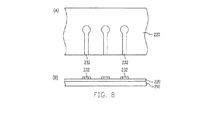
図6から図8は、本発明の実施の形態によるフォトレジストの欠点を検査および修復する方法を示し、プリント回路基板のある領域での回路の一部分の概略図であり、各図の(A)部分は概略的な平面図であり、各図の(B)部分は概略的な側面図である。本発明のフォトレジストの欠陥を検査および修復する方法は以下のステップを含む。まず、図6を参照すると、少なくとも1つの膜220を有する基板210が提供され、膜220は例えば金属層であっても良く、一方、その金属層は例えば銅箔であっても良い。そして、図7を参照すると、パターン化されたフォトレジスト層232が、例えばインクジェット印刷方法によって直接的に膜220上に形成される。次に、パターン化されたフォトレジスト層232が欠陥232aを有するか否かを例えば自動光学検査機を通して検査するために光学検査処理が実行される。その後、図7及び図8を参照すると、パターン化されたフォトレジスト層232の欠陥232aが発生すると、パターン化されたフォトレジスト層232の欠陥232aは修復され、その結果、パターン化されたフォトレジスト層232の外観はさらによくなる。
FIGS. 6 to 8 show a method for inspecting and repairing a defect of a photoresist according to an embodiment of the present invention, and is a schematic view of a part of a circuit in an area of a printed circuit board. The part is a schematic plan view, and the part (B) in each figure is a schematic side view. The method for inspecting and repairing photoresist defects of the present invention includes the following steps. First, referring to FIG. 6, a
図9から図10は、本発明の一実施の形態によるプリント回路基板の製造プロセスを示し、膜をパターン化するステップの概略図である。本発明の一実施の形態によれば、パターン化されたフォトレジスト層232の欠陥232aが修復された後で、その方法はさらに以下のステップを含んでも良い。まず、図9を参照すると、膜220を膜パターン222にパターン化するために、パターン化されたフォトレジスト層232を介して膜220の上でエッチングプロセスが実行される。次に、図10を参照すると、パターン化されたフォトレジスト層232が膜パターン222を露光するために取り除かれ、膜220が例えば金属層であるときには、本発明のプリント回路基板200の製造プロセスは完了される。すなわち、膜220が例えば金属層である場合、図6から図10は本発明の一実施の形態によるプリント回路基板の製造プロセスの概略図を示す。
9 to 10 show a manufacturing process of a printed circuit board according to an embodiment of the present invention and are schematic diagrams of steps for patterning a film. According to one embodiment of the present invention, after the defect 232a of the patterned
本発明の他の実施の形態によると、パターン化されたフォトレジスト層232の欠陥232aを検査した後に、その方法はさらに以下のステップを含む。図7を参照すると、パターン化されたフォトレジスト層232の欠陥232aは座標により分類および位置決めされる。本発明の一実施の形態によれば、パターン化されたフォトレジスト層232の欠陥232aは、例えば、間隙234及び突起236に分類されても良い。
According to another embodiment of the present invention, after inspecting the defect 232a of the patterned
図11は、本発明の一実施の形態による、フォトレジストの欠陥を検査および修復する方法を示し、パターン化されたフォトレジスト層の間隙が取り除かれた状態での概略図である。図7及び図11を参照すると、本発明の他の実施の形態によれば、パターン化されたフォトレジスト層232の欠陥232aが、例えば図7で示されるような幾つかの間隙234からなる場合、間隙234を充填するためにインクジェット印刷方法が実行され、インクジェット印刷方法は、例えば熱気泡インクジェット印刷方法または圧電インクジェット印刷方法である。パターン化されたフォトレジスト層232の欠陥232aが、例えば図7で示されるような幾つかの突起236からなる場合、突起236を取り除くためにレーザ方法が実行され、そのレーザ光は例えば赤外線または紫外線である。
FIG. 11 illustrates a method for inspecting and repairing photoresist defects, according to one embodiment of the present invention, with the patterned photoresist layer gap removed. Referring to FIGS. 7 and 11, according to another embodiment of the present invention, if a defect 232a in the patterned
なお、本発明のプリント回路基板200の製造プロセスでは、多くのプロセス欠陥(例えば、マスク自体が引っかき傷または汚れを有しまたは現像装置の現像タンクが清潔に洗浄されていないこと)によりマスク及び現像を介した露光後に、フォトレジスト層230が、図7で示されたパターン化されたフォトレジスト層232の間隙234または突起236などの多くの欠陥232aを有する可能性もある。しかしながら、本発明によれば、フォトレジスト層230が露光および現像された後で、パターン化されたフォトレジスト層232を徹底的に検査するために例えば自動光学検査機によって光学検査が実施される。パターン化されたフォトレジスト層232の欠陥232aは、パターン化されたフォトレジスト層232の間隙234を充填するために、例えばインクジェット印刷方法によって、または、例えば、パターン化されたフォトレジスト層232の突起236を取り除くレーザ方法によって修復できる。
In the manufacturing process of the printed circuit board 200 of the present invention, the mask and the development are caused by many process defects (for example, the mask itself has scratches or dirt or the developing tank of the developing device is not cleaned cleanly). After exposure via, the photoresist layer 230 may have many defects 232a, such as the
次に、修復された欠陥232aを持つパターン化されたフォトレジスト層232を介して膜220上にエッチングプロセスが実行された後、結果として生じる膜パターン222の欠点はより少なくなり、従来の開回路及び短絡はほとんど発生し得ない。それにより、プリント回路基板200の不良品発生率は効果的に減少し、プリント回路基板200の全体的な製造コストを削減できるようにしている。
Next, after the etching process is performed on the
なお、図2から図3で示される露光及び現像により形成される従来のフォトレジストパターン132と比較すると、パターン化されたフォトレジスト層232は、本発明によるインクジェット印刷方法によって膜220上に直接的に形成できるため、結果として生じる欠陥232aがフォトレジストパターン132の欠陥よりも少ない。したがって、本発明の一実施の形態によれば、パターン化されたフォトレジスト層232が本発明によるインクジェット印刷方法により形成されると、以後の光学検査により必要とされる欠陥232aの検査及び修復の時間は、そのより少ない欠陥232aのために効果的に低減されることがあり、それにより、プリント回路基板200の製造コストをさらに削減する。
Compared to the
もちろん、本発明による、フォトレジストの欠陥を検査および修復するための方法とプリント回路基板の製造プロセスとでは、パターン化されたフォトレジスト層を形成するステップは、露光及び現像によって達成することもでき、インクジェット印刷方法に限定されない。しかしながら、パターン化されたフォトレジスト層がインクジェット印刷方法によって形成されると、それ以後の欠陥検査及び欠陥修復の時間及びコストは、得られパターン化されたフォトレジスト層のより少ない欠陥のためにさらに削減できる。 Of course, in the method and the printed circuit board manufacturing process for inspecting and repairing photoresist defects according to the present invention, the step of forming the patterned photoresist layer can also be accomplished by exposure and development. The inkjet printing method is not limited. However, once the patterned photoresist layer is formed by the inkjet printing method, the time and cost of subsequent defect inspection and defect repair is further increased due to fewer defects in the resulting patterned photoresist layer. Can be reduced.
要するに、光学検査は、パターン化されたフォトレジスト層が欠陥を有するか否かを検査するためにパターン化されたフォトレジスト層を形成した後に実行され、本発明におけるフォトレジストの欠陥を検査および修復する方法とプリント回路基板の製造プロセスとに従って、欠陥は修復できる。欠陥が修復されている状態でのパターン化されたフォトレジスト層を使用することにより膜がエッチングされるので、膜の欠陥はより少なくすることができ、したがって開回路及び短絡はほとんど発生しない。プリント回路基板の不良品発生率は効果的に減少され、プリント回路基板の全体的な製造コストを削減できるようにしている。 In short, the optical inspection is performed after forming the patterned photoresist layer to inspect whether the patterned photoresist layer has defects, and inspects and repairs the defects of the photoresist in the present invention. The defect can be repaired according to the method and the printed circuit board manufacturing process. Since the film is etched by using the patterned photoresist layer with the defect repaired, the film can have fewer defects, and therefore few open circuits and shorts occur. The occurrence rate of defective products on the printed circuit board is effectively reduced, so that the overall manufacturing cost of the printed circuit board can be reduced.
さらに、パターン化されたフォトレジスト層が本発明によるインクジェット印刷方法により形成される場合、以後の欠陥検査および修復プロセスの時間及びコストは、得られたパターン化されたフォトレジスト層のさらに少ない欠陥のために効果的に削減でき、それによりプリント回路基板の製造コストはさらに削減される。 Furthermore, when the patterned photoresist layer is formed by the ink jet printing method according to the present invention, the time and cost of the subsequent defect inspection and repair process can be reduced with fewer defects in the resulting patterned photoresist layer. Therefore, the manufacturing cost of the printed circuit board can be further reduced.
本発明は好ましい実施の形態を参照して前述されたけれども、本発明がそのような記述によって制限されることを意図されず添付の請求項により定義されるような発明の趣旨及び請求の範囲から逸脱することなく変更及び変形が当業者によってなされ得ることが理解される。 Although the present invention has been described above with reference to preferred embodiments, it is not intended that the invention be limited by such description, but rather from the spirit and scope of the invention as defined by the appended claims. It will be understood that modifications and variations can be made by those skilled in the art without departing.
Claims (16)
少なくとも1つの膜を有する基板を提供するステップと、
前記膜にパターン化されたフォトレジスト層を形成するステップと、
前記パターン化されたフォトレジスト層が欠陥を有するか否かを検査するために光学検査を実行するステップと、
前記パターン化されたフォトレジスト層が前記欠陥を有する場合に前記パターン化されたフォトレジスト層の前記欠陥を修復するステップとを有し、
前記欠陥が間隙である場合には、前記間隙を充填するために熱気泡インクジェット印刷方法を実行し、
前記欠陥が突起である場合には、前記突起を取り除くためにレーザ方法を実行することを特徴とするフォトレジストの欠陥を検査および修復する方法。 A method for inspecting and repairing defects in a photoresist that is suitable for a printed circuit board manufacturing process comprising:
Providing a substrate having at least one film;
Forming a patterned photoresist layer on the film;
Performing an optical inspection to inspect whether the patterned photoresist layer has defects;
Repairing the defects in the patterned photoresist layer if the patterned photoresist layer has the defects;
If the defect is a gap, perform a hot bubble inkjet printing method to fill the gap,
A method for inspecting and repairing a defect in a photoresist, wherein if the defect is a protrusion, a laser method is performed to remove the protrusion.
少なくとも1つの膜を有する基板を提供するステップと、
前記膜にパターン化されたフォトレジスト層を形成するステップと、
前記パターン化されたフォトレジスト層が欠陥を有するか否かを検査するために光学検査を実行するステップと、
前記パターン化されたフォトレジスト層が前記欠陥を有する場合に前記パターン化されたフォトレジスト層の前記欠陥を修復するステップとを有し、
前記欠陥が間隙である場合には、前記間隙を充填するために圧電インクジェット印刷方法を実行し、
前記欠陥が突起である場合には、前記突起を取り除くためにレーザ方法を実行することを特徴とするフォトレジストの欠陥を検査および修復する方法。 A method for inspecting and repairing photoresist defects, suitable for a printed circuit board manufacturing process, comprising:
Providing a substrate having at least one film;
Forming a patterned photoresist layer on the film;
Performing an optical inspection to inspect whether the patterned photoresist layer has defects;
Repairing the defects in the patterned photoresist layer if the patterned photoresist layer has the defects;
If the defect is a gap, perform a piezoelectric inkjet printing method to fill the gap,
A method for inspecting and repairing a defect in a photoresist, wherein if the defect is a protrusion, a laser method is performed to remove the protrusion.
前記パターン化されたフォトレジスト層の前記欠陥を分類するステップと、
座標により前記パターン化されたフォトレジスト層の前記欠陥を位置決めするステップとをさらに有することを特徴とする請求項1に記載のフォトレジストの欠陥を検査および修復する方法。 After inspecting the defects in the patterned photoresist layer, the method comprises:
Classifying the defects in the patterned photoresist layer;
The method of inspecting and repairing photoresist defects according to claim 1, further comprising positioning the defects in the patterned photoresist layer by coordinates.
前記パターン化されたフォトレジスト層の前記欠陥を分類するステップと、
座標により前記パターン化されたフォトレジスト層の前記欠陥を位置決めするステップとをさらに有することを特徴とする請求項2に記載のフォトレジストの欠陥を検査および修復する方法。 After inspecting the defects in the patterned photoresist layer, the method comprises:
Classifying the defects in the patterned photoresist layer;
3. The method of inspecting and repairing photoresist defects according to claim 2, further comprising positioning the defects in the patterned photoresist layer by coordinates.
前記膜をパターン化するために前記膜の上でエッチングプロセスを実行するステップと
、
前記パターン化されたフォトレジスト層を取り除くステップとをさらに備えていることを特徴とする請求項1に記載のフォトレジストの欠陥を検査および修復する方法。 After removing the defects in the patterned photoresist layer, the method comprises:
Performing an etching process on the film to pattern the film;
The method of claim 1 further comprising the step of removing the patterned photoresist layer.
前記膜をパターン化するために前記膜の上でエッチングプロセスを実行するステップと、
前記パターン化されたフォトレジスト層を取り除くステップとをさらに備えていることを特徴とする請求項2に記載のフォトレジストの欠陥を検査および修復する方法。 After removing the defects in the patterned photoresist layer, the method comprises:
Performing an etching process on the film to pattern the film;
3. The method of inspecting and repairing a photoresist defect according to claim 2, further comprising the step of removing the patterned photoresist layer.
少なくとも1つの金属層を有する基板を提供するステップと、
前記金属層にパターン化されたフォトレジスト層を形成するステップと、
前記パターン化されたフォトレジスト層が欠陥を有するか否かを検査するために光学検査を実行するステップと、
前記パターン化されたフォトレジスト層が前記欠陥を有する場合に、前記パターン化されたフォトレジスト層の前記欠陥を修復するステップと、
前記金属層をパターン化するために前記金属層にエッチングプロセスを実行するステップと、
前記パターン化されたフォトレジスト層を取り除くステップとを含み、
前記欠陥が間隙である場合には、前記間隙を充填するために熱気泡インクジェット印刷方法または圧電インクジェット印刷方法を実行し、
前記欠陥が突起である場合には、前記突起を取り除くためにレーザ方法を実行することを特徴とするプリント回路基板の製造プロセス。 A printed circuit board manufacturing process,
Providing a substrate having at least one metal layer;
Forming a patterned photoresist layer on the metal layer;
Performing an optical inspection to inspect whether the patterned photoresist layer has defects;
Repairing the defects in the patterned photoresist layer if the patterned photoresist layer has the defects;
Performing an etching process on the metal layer to pattern the metal layer;
Removing the patterned photoresist layer;
If the defect is a gap, perform a hot bubble inkjet printing method or a piezoelectric inkjet printing method to fill the gap,
If the defect is a protrusion, a laser circuit method is performed to remove the protrusion, and the printed circuit board manufacturing process is characterized.
前記パターン化されたフォトレジスト層の前記欠陥を分類するステップと、
座標により前記パターン化されたフォトレジスト層の前記欠陥を位置決めするステップとをさらに含むことを特徴とする請求項13に記載のプリント回路基板の製造プロセス。 After inspecting the defects in the patterned photoresist layer, the process comprises:
Classifying the defects in the patterned photoresist layer;
The printed circuit board manufacturing process of claim 13, further comprising positioning the defect in the patterned photoresist layer by coordinates.
The printed circuit board manufacturing process of claim 13, wherein the patterned photoresist layer is formed on the metal layer by an inkjet printing method.
Applications Claiming Priority (1)
| Application Number | Priority Date | Filing Date | Title |
|---|---|---|---|
| TW094135481A TWI301737B (en) | 2005-10-12 | 2005-10-12 | Method for inspecting and mending defects of photo-resist and manufacturing process of printed circuit board |
Publications (2)
| Publication Number | Publication Date |
|---|---|
| JP2007110065A JP2007110065A (en) | 2007-04-26 |
| JP4583317B2 true JP4583317B2 (en) | 2010-11-17 |
Family
ID=37948617
Family Applications (1)
| Application Number | Title | Priority Date | Filing Date |
|---|---|---|---|
| JP2006030300A Expired - Fee Related JP4583317B2 (en) | 2005-10-12 | 2006-02-07 | Method for inspecting and repairing defects in photoresist, and printed circuit board manufacturing process |
Country Status (3)
| Country | Link |
|---|---|
| US (1) | US20070087457A1 (en) |
| JP (1) | JP4583317B2 (en) |
| TW (1) | TWI301737B (en) |
Families Citing this family (10)
| Publication number | Priority date | Publication date | Assignee | Title |
|---|---|---|---|---|
| JP5338214B2 (en) * | 2008-09-11 | 2013-11-13 | 凸版印刷株式会社 | Printing method |
| JP5338215B2 (en) * | 2008-09-11 | 2013-11-13 | 凸版印刷株式会社 | Printing method |
| KR101452190B1 (en) | 2013-02-20 | 2014-10-22 | 주식회사 스마트코리아피씨비 | Method for manufacturing multi-layer pcb |
| WO2016014047A1 (en) * | 2014-07-23 | 2016-01-28 | Apple Inc. | Adaptive processes for improving integrity of surfaces |
| US10649497B2 (en) | 2014-07-23 | 2020-05-12 | Apple Inc. | Adaptive processes for improving integrity of surfaces |
| JP2016054276A (en) * | 2014-09-04 | 2016-04-14 | 株式会社東芝 | Semiconductor device manufacturing method |
| CN107290353A (en) * | 2016-03-30 | 2017-10-24 | 中芯国际集成电路制造(上海)有限公司 | The bubble detection device and detection method of photoresistance pipeline |
| KR20220110861A (en) * | 2019-02-14 | 2022-08-09 | 오르보테크 엘티디. | A method and apparatus for preparing a pcb product having highly dense conductors |
| CN110824832A (en) * | 2019-11-12 | 2020-02-21 | 上海集成电路研发中心有限公司 | A kind of defect repair method of extreme ultraviolet photomask |
| CN112557417B (en) * | 2021-02-28 | 2021-05-11 | 深圳宜美智科技股份有限公司 | PCB laser repairing method and device based on image detection |
Family Cites Families (2)
| Publication number | Priority date | Publication date | Assignee | Title |
|---|---|---|---|---|
| JP2003050256A (en) * | 2001-08-08 | 2003-02-21 | Hitachi Ltd | Inspection device for printed circuit board |
| JP2005302751A (en) * | 2004-04-06 | 2005-10-27 | Mitsubishi Electric Corp | Resist pattern formation method and apparatus thereof, and display manufacturing method and apparatus thereof |
-
2005
- 2005-10-12 TW TW094135481A patent/TWI301737B/en not_active IP Right Cessation
- 2005-12-08 US US11/164,855 patent/US20070087457A1/en not_active Abandoned
-
2006
- 2006-02-07 JP JP2006030300A patent/JP4583317B2/en not_active Expired - Fee Related
Also Published As
| Publication number | Publication date |
|---|---|
| TW200715923A (en) | 2007-04-16 |
| US20070087457A1 (en) | 2007-04-19 |
| TWI301737B (en) | 2008-10-01 |
| JP2007110065A (en) | 2007-04-26 |
Similar Documents
| Publication | Publication Date | Title |
|---|---|---|
| JP4583317B2 (en) | Method for inspecting and repairing defects in photoresist, and printed circuit board manufacturing process | |
| KR100774048B1 (en) | Method for manufacturing photomask and photomask blanks, and recycling photomask | |
| CN107148159A (en) | The method for manufacturing printed substrate | |
| CN101566788A (en) | Method for repairing photoresist pattern | |
| KR101572089B1 (en) | Method of defect inspection for printed circuit board | |
| CN101203091A (en) | Circuit board repairing method | |
| JP2005142254A (en) | Wiring board and manufacturing method therefor | |
| US5902717A (en) | Method of fabricating semiconductor device using half-tone phase shift mask | |
| KR20200094587A (en) | Apparatus and method for repairing faulty solder using laser | |
| JP2008181998A (en) | Build-up substrate and manufacturing method thereof, and inspection method | |
| JP4446845B2 (en) | Printed circuit board manufacturing method and manufacturing apparatus | |
| JP2006165106A (en) | Electronic component mounting method | |
| JP4823605B2 (en) | Exposure apparatus, exposure method, and pattern manufacturing system | |
| JP2944589B2 (en) | COB mounting board and method of mounting IC chip on the board | |
| US8685631B2 (en) | Inspection method for patterning of photoresist | |
| JP7403875B1 (en) | Method for repairing printed wiring boards and method for manufacturing recycled printed wiring boards | |
| KR101022869B1 (en) | Manufacturing Method of Printed Circuit Board for Image Sensor Module | |
| JP2009105400A (en) | Manufacturing method for flexible printed circuit board, and inspection method therefor | |
| Ehsani et al. | Lasers speed up board production | |
| KR20040046194A (en) | pattern inspector structure of circuit board | |
| JP2007081293A (en) | Inspection method, method of manufacturing semiconductor device and program | |
| CN117098326A (en) | PCB green oil bridge anti-drop treatment method | |
| JP2005043793A (en) | Photomask and pattern transfer method using the same | |
| JP2000181074A (en) | Method for exposing photosensitive layer | |
| CN119342703A (en) | PCB board gold finger wiring method, device and printed circuit board |
Legal Events
| Date | Code | Title | Description |
|---|---|---|---|
| A131 | Notification of reasons for refusal |
Free format text: JAPANESE INTERMEDIATE CODE: A131 Effective date: 20071211 |
|
| A521 | Written amendment |
Free format text: JAPANESE INTERMEDIATE CODE: A523 Effective date: 20080311 |
|
| A02 | Decision of refusal |
Free format text: JAPANESE INTERMEDIATE CODE: A02 Effective date: 20080401 |
|
| A521 | Written amendment |
Free format text: JAPANESE INTERMEDIATE CODE: A523 Effective date: 20080630 |
|
| A911 | Transfer to examiner for re-examination before appeal (zenchi) |
Free format text: JAPANESE INTERMEDIATE CODE: A911 Effective date: 20080808 |
|
| A912 | Re-examination (zenchi) completed and case transferred to appeal board |
Free format text: JAPANESE INTERMEDIATE CODE: A912 Effective date: 20081107 |
|
| A521 | Written amendment |
Free format text: JAPANESE INTERMEDIATE CODE: A523 Effective date: 20100701 |
|
| A01 | Written decision to grant a patent or to grant a registration (utility model) |
Free format text: JAPANESE INTERMEDIATE CODE: A01 |
|
| A61 | First payment of annual fees (during grant procedure) |
Free format text: JAPANESE INTERMEDIATE CODE: A61 Effective date: 20100831 |
|
| R150 | Certificate of patent or registration of utility model |
Free format text: JAPANESE INTERMEDIATE CODE: R150 |
|
| FPAY | Renewal fee payment (event date is renewal date of database) |
Free format text: PAYMENT UNTIL: 20130910 Year of fee payment: 3 |
|
| R250 | Receipt of annual fees |
Free format text: JAPANESE INTERMEDIATE CODE: R250 |
|
| LAPS | Cancellation because of no payment of annual fees |