JP4238779B2 - 圧電発振器および電子機器 - Google Patents
圧電発振器および電子機器 Download PDFInfo
- Publication number
- JP4238779B2 JP4238779B2 JP2004158519A JP2004158519A JP4238779B2 JP 4238779 B2 JP4238779 B2 JP 4238779B2 JP 2004158519 A JP2004158519 A JP 2004158519A JP 2004158519 A JP2004158519 A JP 2004158519A JP 4238779 B2 JP4238779 B2 JP 4238779B2
- Authority
- JP
- Japan
- Prior art keywords
- electronic component
- piezoelectric oscillator
- piezoelectric
- lead
- mounting
- Prior art date
- Legal status (The legal status is an assumption and is not a legal conclusion. Google has not performed a legal analysis and makes no representation as to the accuracy of the status listed.)
- Expired - Fee Related
Links
- 239000000463 material Substances 0.000 claims description 43
- 239000004020 conductor Substances 0.000 claims description 33
- 239000012778 molding material Substances 0.000 claims description 10
- 239000011347 resin Substances 0.000 description 100
- 229920005989 resin Polymers 0.000 description 100
- 230000005284 excitation Effects 0.000 description 23
- 230000010355 oscillation Effects 0.000 description 23
- 239000000758 substrate Substances 0.000 description 14
- 239000003990 capacitor Substances 0.000 description 12
- 235000014676 Phragmites communis Nutrition 0.000 description 11
- 238000005452 bending Methods 0.000 description 10
- 238000010586 diagram Methods 0.000 description 10
- 238000005530 etching Methods 0.000 description 10
- 238000007747 plating Methods 0.000 description 9
- 239000002184 metal Substances 0.000 description 7
- 229910052751 metal Inorganic materials 0.000 description 7
- 238000005219 brazing Methods 0.000 description 5
- 239000000919 ceramic Substances 0.000 description 5
- 239000011521 glass Substances 0.000 description 5
- 238000000465 moulding Methods 0.000 description 5
- 230000015572 biosynthetic process Effects 0.000 description 4
- 238000005520 cutting process Methods 0.000 description 4
- 238000007789 sealing Methods 0.000 description 4
- 238000010897 surface acoustic wave method Methods 0.000 description 4
- 230000005540 biological transmission Effects 0.000 description 3
- 238000007689 inspection Methods 0.000 description 3
- 150000002500 ions Chemical class 0.000 description 3
- 238000004519 manufacturing process Methods 0.000 description 3
- 238000000034 method Methods 0.000 description 3
- 230000004048 modification Effects 0.000 description 3
- 238000012986 modification Methods 0.000 description 3
- 230000000149 penetrating effect Effects 0.000 description 3
- 238000005096 rolling process Methods 0.000 description 3
- IJGRMHOSHXDMSA-UHFFFAOYSA-N Atomic nitrogen Chemical compound N#N IJGRMHOSHXDMSA-UHFFFAOYSA-N 0.000 description 2
- PXHVJJICTQNCMI-UHFFFAOYSA-N Nickel Chemical compound [Ni] PXHVJJICTQNCMI-UHFFFAOYSA-N 0.000 description 2
- 239000000853 adhesive Substances 0.000 description 2
- 230000001070 adhesive effect Effects 0.000 description 2
- 230000007423 decrease Effects 0.000 description 2
- 230000000694 effects Effects 0.000 description 2
- 230000006870 function Effects 0.000 description 2
- 230000001678 irradiating effect Effects 0.000 description 2
- 239000007788 liquid Substances 0.000 description 2
- 229910000679 solder Inorganic materials 0.000 description 2
- 229910000881 Cu alloy Inorganic materials 0.000 description 1
- 239000004593 Epoxy Substances 0.000 description 1
- 229910000640 Fe alloy Inorganic materials 0.000 description 1
- 230000001413 cellular effect Effects 0.000 description 1
- 238000005336 cracking Methods 0.000 description 1
- 239000013078 crystal Substances 0.000 description 1
- 230000002950 deficient Effects 0.000 description 1
- 238000009713 electroplating Methods 0.000 description 1
- 239000007789 gas Substances 0.000 description 1
- PCHJSUWPFVWCPO-UHFFFAOYSA-N gold Chemical compound [Au] PCHJSUWPFVWCPO-UHFFFAOYSA-N 0.000 description 1
- 239000010931 gold Substances 0.000 description 1
- 229910052737 gold Inorganic materials 0.000 description 1
- 239000011261 inert gas Substances 0.000 description 1
- 238000002347 injection Methods 0.000 description 1
- 239000007924 injection Substances 0.000 description 1
- 238000002844 melting Methods 0.000 description 1
- 230000008018 melting Effects 0.000 description 1
- 239000007769 metal material Substances 0.000 description 1
- 229910052759 nickel Inorganic materials 0.000 description 1
- 229910052757 nitrogen Inorganic materials 0.000 description 1
- 230000002093 peripheral effect Effects 0.000 description 1
- 230000035945 sensitivity Effects 0.000 description 1
- 230000008054 signal transmission Effects 0.000 description 1
- 239000000126 substance Substances 0.000 description 1
- 229920001187 thermosetting polymer Polymers 0.000 description 1
Images


Classifications
-
- H—ELECTRICITY
- H03—ELECTRONIC CIRCUITRY
- H03H—IMPEDANCE NETWORKS, e.g. RESONANT CIRCUITS; RESONATORS
- H03H9/00—Networks comprising electromechanical or electro-acoustic elements; Electromechanical resonators
- H03H9/02—Details
- H03H9/05—Holders or supports
- H03H9/0538—Constructional combinations of supports or holders with electromechanical or other electronic elements
- H03H9/0547—Constructional combinations of supports or holders with electromechanical or other electronic elements consisting of a vertical arrangement
-
- H—ELECTRICITY
- H03—ELECTRONIC CIRCUITRY
- H03H—IMPEDANCE NETWORKS, e.g. RESONANT CIRCUITS; RESONATORS
- H03H9/00—Networks comprising electromechanical or electro-acoustic elements; Electromechanical resonators
- H03H9/02—Details
- H03H9/05—Holders or supports
- H03H9/0504—Holders or supports for bulk acoustic wave devices
- H03H9/0514—Holders or supports for bulk acoustic wave devices consisting of mounting pads or bumps
-
- H—ELECTRICITY
- H03—ELECTRONIC CIRCUITRY
- H03H—IMPEDANCE NETWORKS, e.g. RESONANT CIRCUITS; RESONATORS
- H03H9/00—Networks comprising electromechanical or electro-acoustic elements; Electromechanical resonators
- H03H9/02—Details
- H03H9/05—Holders or supports
- H03H9/10—Mounting in enclosures
- H03H9/1007—Mounting in enclosures for bulk acoustic wave [BAW] devices
- H03H9/1014—Mounting in enclosures for bulk acoustic wave [BAW] devices the enclosure being defined by a frame built on a substrate and a cap, the frame having no mechanical contact with the BAW device
-
- H—ELECTRICITY
- H01—ELECTRIC ELEMENTS
- H01L—SEMICONDUCTOR DEVICES NOT COVERED BY CLASS H10
- H01L2224/00—Indexing scheme for arrangements for connecting or disconnecting semiconductor or solid-state bodies and methods related thereto as covered by H01L24/00
- H01L2224/01—Means for bonding being attached to, or being formed on, the surface to be connected, e.g. chip-to-package, die-attach, "first-level" interconnects; Manufacturing methods related thereto
- H01L2224/10—Bump connectors; Manufacturing methods related thereto
- H01L2224/15—Structure, shape, material or disposition of the bump connectors after the connecting process
- H01L2224/16—Structure, shape, material or disposition of the bump connectors after the connecting process of an individual bump connector
- H01L2224/161—Disposition
- H01L2224/16151—Disposition the bump connector connecting between a semiconductor or solid-state body and an item not being a semiconductor or solid-state body, e.g. chip-to-substrate, chip-to-passive
- H01L2224/16221—Disposition the bump connector connecting between a semiconductor or solid-state body and an item not being a semiconductor or solid-state body, e.g. chip-to-substrate, chip-to-passive the body and the item being stacked
- H01L2224/16245—Disposition the bump connector connecting between a semiconductor or solid-state body and an item not being a semiconductor or solid-state body, e.g. chip-to-substrate, chip-to-passive the body and the item being stacked the item being metallic
-
- H—ELECTRICITY
- H01—ELECTRIC ELEMENTS
- H01L—SEMICONDUCTOR DEVICES NOT COVERED BY CLASS H10
- H01L2224/00—Indexing scheme for arrangements for connecting or disconnecting semiconductor or solid-state bodies and methods related thereto as covered by H01L24/00
- H01L2224/01—Means for bonding being attached to, or being formed on, the surface to be connected, e.g. chip-to-package, die-attach, "first-level" interconnects; Manufacturing methods related thereto
- H01L2224/42—Wire connectors; Manufacturing methods related thereto
- H01L2224/47—Structure, shape, material or disposition of the wire connectors after the connecting process
- H01L2224/48—Structure, shape, material or disposition of the wire connectors after the connecting process of an individual wire connector
- H01L2224/481—Disposition
- H01L2224/48151—Connecting between a semiconductor or solid-state body and an item not being a semiconductor or solid-state body, e.g. chip-to-substrate, chip-to-passive
- H01L2224/48221—Connecting between a semiconductor or solid-state body and an item not being a semiconductor or solid-state body, e.g. chip-to-substrate, chip-to-passive the body and the item being stacked
- H01L2224/48245—Connecting between a semiconductor or solid-state body and an item not being a semiconductor or solid-state body, e.g. chip-to-substrate, chip-to-passive the body and the item being stacked the item being metallic
- H01L2224/48247—Connecting between a semiconductor or solid-state body and an item not being a semiconductor or solid-state body, e.g. chip-to-substrate, chip-to-passive the body and the item being stacked the item being metallic connecting the wire to a bond pad of the item
Landscapes
- Physics & Mathematics (AREA)
- Acoustics & Sound (AREA)
- Oscillators With Electromechanical Resonators (AREA)
- Piezo-Electric Or Mechanical Vibrators, Or Delay Or Filter Circuits (AREA)
Description
また本発明は、薄型化を可能にした圧電発振器を搭載した電子機器を提供することを目的とする。
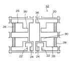
なお、実装端子形成用リード26に形成された部品接続端子30を接続端子24のように先端部分の幅を大きくしてもよい。これにより、実装端子形成用リード26と樹脂パッケージ16の接着強度を強くすることができ、実装端子形成用リード26を折り曲げる際に、実装端子形成用リード26が樹脂パッケージ16から抜けることを防ぐことができる。
また上述した圧電発振器70では、実装端子76の実装面と電子部品14の表面とが同一平面内にあるが、他の実施形態として、傾斜部80により形成される段差の距離を大きくして、電子部品14の表面をモールド樹脂で覆ってもよい。
最後に、電子部品14に搭載されている容量アレイの容量調整または可変容量ダイオードに供給される電圧を調整することにより、もう一度圧電発振器90の発振周波数が調整される。このようにして圧電発振器90が製造される。
また実装端子98は、樹脂パッケージ16の裏面全面を使用して形成できる。すなわち圧電発振器90の裏面は樹脂パッケージ16のみであり、電子部品14等が露出していないので、実装端子98と電子部品14とが上下に重ねて配置させることができる。したがって実装端子98を大きく形成でき、実装端子98と実装基板との間の接合強度を向上させることができる。
なお、第3の実施形態に係る圧電発振器90において、実装端子と接続端子を反対に形成してもよい。つまり、実装端子98はリード92により形成し、接続端子はリード92と穴部を介して接続して形成してもよい。
Claims (9)
- リードフレームから形成した複数のリードの一側面に電気的に接続した電子部品と、
前記複数のリードの一部に接続されて前記電子部品側に折り曲げて部品接続端子との間に段差を形成した複数の実装端子と、
前記複数のリードの他側面と前記複数の実装端子の実装面とを露出させて前記電子部品を封止したモールド材と、
前記リードの他側面に導電材を介して接合した圧電振動片と、
を有することを特徴とする圧電発振器。 - 前記実装端子の実装面と前記電子部品の表面とは同一面内にあることを特徴とする請求項1に記載の圧電発振器。
- リードフレームから形成した複数のリードの一側面に電気的に接続した電子部品と、
前記複数のリードの一部に接続されて前記電子部品が実装されるリード面との間に段差を形成した接続端子と、
前記複数のリードの他側面と前記接続端子の接続面とを露出させて前記電子部品を封止したモールド材と、
前記接続端子の接続面に導電材を介して接合した圧電振動片と、
を有することを特徴とする圧電発振器。 - 前記接続端子の接続面と前記電子部品の表面とは同一面内にあることを特徴とする請求項3に記載の圧電発振器。
- 前記電子部品の前記リードへの電気的接続は、フリップチップボンディングにより行うことを特徴とする請求項1ないし4のいずれかに記載の圧電発振器。
- リードフレームから形成した複数のリードの一側面に電気的に接続した電子部品と、
前記複数のリードの他側面を露出させて前記電子部品を封止したモールド材と、
前記複数のリードの他側面に、導電材を介して接合した圧電振動片と、
前記モールド材の一部に穴部が設けられ、前記穴部に形成された配線を介して前記リードと電気的に接続された実装端子と、
を有することを特徴とする圧電発振器。 - 前記圧電振動片が実装される側に向く前記モールド材の表面に耐湿材を塗布したことを特徴とする請求項1ないし6のいずれかに記載の圧電発振器。
- 前記電子部品と前記圧電振動片との間に熱伝導材を設けたことを特徴とする請求項1ないし7のいずれかに記載の圧電発振器。
- 請求項1ないし8のいずれかに記載の圧電発振器を備えたことを特徴とする電子機器。
Priority Applications (2)
| Application Number | Priority Date | Filing Date | Title |
|---|---|---|---|
| JP2004158519A JP4238779B2 (ja) | 2004-05-28 | 2004-05-28 | 圧電発振器および電子機器 |
| US11/138,288 US20050264140A1 (en) | 2004-05-28 | 2005-05-27 | Piezoelectric oscillator and electronic device |
Applications Claiming Priority (1)
| Application Number | Priority Date | Filing Date | Title |
|---|---|---|---|
| JP2004158519A JP4238779B2 (ja) | 2004-05-28 | 2004-05-28 | 圧電発振器および電子機器 |
Publications (2)
| Publication Number | Publication Date |
|---|---|
| JP2005341326A JP2005341326A (ja) | 2005-12-08 |
| JP4238779B2 true JP4238779B2 (ja) | 2009-03-18 |
Family
ID=35424413
Family Applications (1)
| Application Number | Title | Priority Date | Filing Date |
|---|---|---|---|
| JP2004158519A Expired - Fee Related JP4238779B2 (ja) | 2004-05-28 | 2004-05-28 | 圧電発振器および電子機器 |
Country Status (2)
| Country | Link |
|---|---|
| US (1) | US20050264140A1 (ja) |
| JP (1) | JP4238779B2 (ja) |
Families Citing this family (14)
| Publication number | Priority date | Publication date | Assignee | Title |
|---|---|---|---|---|
| US7694734B2 (en) * | 2005-10-31 | 2010-04-13 | Baker Hughes Incorporated | Method and apparatus for insulating a resonator downhole |
| WO2007147137A2 (en) | 2006-06-15 | 2007-12-21 | Sitime Corporation | Stacked die package for mems resonator system |
| JP5111018B2 (ja) * | 2007-08-27 | 2012-12-26 | セイコーインスツル株式会社 | 気密端子の製造方法及び圧電振動子の製造方法 |
| JP5360371B2 (ja) * | 2008-12-16 | 2013-12-04 | セイコーエプソン株式会社 | 電子デバイス |
| US8256288B2 (en) | 2008-12-16 | 2012-09-04 | Seiko Epson Corporation | Sensor device |
| DE102010039599A1 (de) * | 2010-08-20 | 2012-02-23 | Robert Bosch Gmbh | Sensormodul zur Aufnahme eines Drucksensorchips und zur Montage in einem Sensorgehäuse |
| KR20130020331A (ko) * | 2011-08-19 | 2013-02-27 | 삼성전기주식회사 | 초음파 센서 |
| US9230890B2 (en) | 2012-04-27 | 2016-01-05 | Lapis Semiconductor Co., Ltd. | Semiconductor device and measurement device |
| JP6340754B2 (ja) * | 2013-03-29 | 2018-06-13 | セイコーエプソン株式会社 | 電子デバイス、電子機器、移動体、電子デバイスの製造方法 |
| US9754803B2 (en) * | 2013-03-27 | 2017-09-05 | Seiko Epson Corporation | Electronic device, electronic apparatus, moving object, and method for manufacturing electronic device |
| JP2014207313A (ja) * | 2013-04-12 | 2014-10-30 | セイコーエプソン株式会社 | 電子部品、電子機器、および移動体 |
| JP5582323B2 (ja) * | 2013-04-22 | 2014-09-03 | セイコーエプソン株式会社 | 電子デバイス |
| JP6276338B2 (ja) * | 2016-07-25 | 2018-02-07 | ラピスセミコンダクタ株式会社 | 半導体装置及び計測機器 |
| JP7552285B2 (ja) * | 2020-11-24 | 2024-09-18 | セイコーエプソン株式会社 | 発振器および製造方法 |
Family Cites Families (6)
| Publication number | Priority date | Publication date | Assignee | Title |
|---|---|---|---|---|
| US6456168B1 (en) * | 2000-12-29 | 2002-09-24 | Cts Corporation | Temperature compensated crystal oscillator assembled on crystal base |
| US6759913B2 (en) * | 2001-06-29 | 2004-07-06 | Cts Corporation | Crystal resonator based oscillator formed by attaching two separate housings |
| DE10238523B4 (de) * | 2002-08-22 | 2014-10-02 | Epcos Ag | Verkapseltes elektronisches Bauelement und Verfahren zur Herstellung |
| JP3918794B2 (ja) * | 2002-12-10 | 2007-05-23 | セイコーエプソン株式会社 | 圧電発振器およびその製造方法並びに電子機器 |
| JP3783235B2 (ja) * | 2003-06-16 | 2006-06-07 | セイコーエプソン株式会社 | 圧電発振器とその製造方法ならびに圧電発振器を利用した携帯電話装置および圧電発振器を利用した電子機器 |
| JP2006311380A (ja) * | 2005-04-28 | 2006-11-09 | Epson Toyocom Corp | 圧電振動子及び圧電発振器 |
-
2004
- 2004-05-28 JP JP2004158519A patent/JP4238779B2/ja not_active Expired - Fee Related
-
2005
- 2005-05-27 US US11/138,288 patent/US20050264140A1/en not_active Abandoned
Also Published As
| Publication number | Publication date |
|---|---|
| US20050264140A1 (en) | 2005-12-01 |
| JP2005341326A (ja) | 2005-12-08 |
Similar Documents
| Publication | Publication Date | Title |
|---|---|---|
| JP4222147B2 (ja) | 圧電発振器及び圧電発振器を利用した携帯電話装置および圧電発振器を利用した電子機器 | |
| JP4238779B2 (ja) | 圧電発振器および電子機器 | |
| EP2012427A2 (en) | Piezoelectric vibrating pieces and piezoelectric devices | |
| JP2002335128A (ja) | 圧電デバイス | |
| JP2006279872A (ja) | 圧電振動子及びその製造方法並びにその圧電振動子を用いた圧電発振器の製造方法 | |
| EP2355341A2 (en) | Piezoelectric vibrator and oscillator using the same | |
| JP2009188483A (ja) | 圧電デバイス及び表面実装型圧電発振器 | |
| US7872401B2 (en) | Piezoelectric vibrator with hermetically closed casing and filler comprising non-spherical conductive particles | |
| US8281468B2 (en) | Method of manufacturing piezoelectric vibrators | |
| JP4692715B2 (ja) | 圧電発振器、電子機器および圧電発振器の製造方法 | |
| JP2002353766A (ja) | 圧電デバイス | |
| JPWO2010097905A1 (ja) | パッケージの製造方法及び圧電振動子、発振器、電子機器、並びに電波時計 | |
| JP5258957B2 (ja) | 圧電振動子の製造方法及び基板の製造方法 | |
| JPH11186850A (ja) | 圧電発振器 | |
| JP2009194789A (ja) | 圧電振動子の製造方法、圧電振動子、発振器、電子機器及び電波時計 | |
| JP4437694B2 (ja) | 圧電発振器の製造方法、圧電発振器および電子機器 | |
| JP2002280865A (ja) | 圧電デバイス | |
| JP2010124494A (ja) | 圧電発振器、電子機器および圧電発振器の製造方法 | |
| JP4457760B2 (ja) | 圧電発振器および電子機器 | |
| JP4472445B2 (ja) | 圧電発振器の製造方法 | |
| JP2006101181A (ja) | 圧電発振器および電子機器 | |
| JP2005094461A (ja) | 圧電デバイスとその製造方法ならびに圧電デバイスを利用した携帯電話装置および圧電デバイスを利用した電子機器 | |
| JP2006101090A (ja) | 圧電発振器の周波数調整方法、圧電発振器および電子機器 | |
| JP2005260727A (ja) | 圧電振動素子の支持構造および圧電発振器 | |
| JP2006101241A (ja) | 圧電発振器、及びその製造方法 |
Legal Events
| Date | Code | Title | Description |
|---|---|---|---|
| A621 | Written request for application examination |
Free format text: JAPANESE INTERMEDIATE CODE: A621 Effective date: 20051104 |
|
| A977 | Report on retrieval |
Free format text: JAPANESE INTERMEDIATE CODE: A971007 Effective date: 20080225 |
|
| A131 | Notification of reasons for refusal |
Free format text: JAPANESE INTERMEDIATE CODE: A131 Effective date: 20080417 |
|
| A521 | Request for written amendment filed |
Free format text: JAPANESE INTERMEDIATE CODE: A523 Effective date: 20080603 |
|
| TRDD | Decision of grant or rejection written | ||
| A01 | Written decision to grant a patent or to grant a registration (utility model) |
Free format text: JAPANESE INTERMEDIATE CODE: A01 Effective date: 20081125 |
|
| A01 | Written decision to grant a patent or to grant a registration (utility model) |
Free format text: JAPANESE INTERMEDIATE CODE: A01 |
|
| A61 | First payment of annual fees (during grant procedure) |
Free format text: JAPANESE INTERMEDIATE CODE: A61 Effective date: 20081208 |
|
| FPAY | Renewal fee payment (event date is renewal date of database) |
Free format text: PAYMENT UNTIL: 20120109 Year of fee payment: 3 |
|
| R150 | Certificate of patent or registration of utility model |
Free format text: JAPANESE INTERMEDIATE CODE: R150 |
|
| FPAY | Renewal fee payment (event date is renewal date of database) |
Free format text: PAYMENT UNTIL: 20120109 Year of fee payment: 3 |
|
| FPAY | Renewal fee payment (event date is renewal date of database) |
Free format text: PAYMENT UNTIL: 20130109 Year of fee payment: 4 |
|
| FPAY | Renewal fee payment (event date is renewal date of database) |
Free format text: PAYMENT UNTIL: 20130109 Year of fee payment: 4 |
|
| FPAY | Renewal fee payment (event date is renewal date of database) |
Free format text: PAYMENT UNTIL: 20140109 Year of fee payment: 5 |
|
| S531 | Written request for registration of change of domicile |
Free format text: JAPANESE INTERMEDIATE CODE: R313531 |
|
| R350 | Written notification of registration of transfer |
Free format text: JAPANESE INTERMEDIATE CODE: R350 |
|
| LAPS | Cancellation because of no payment of annual fees |