JP4238779B2 - Piezoelectric oscillator and electronic equipment - Google Patents
Piezoelectric oscillator and electronic equipment Download PDFInfo
- Publication number
- JP4238779B2 JP4238779B2 JP2004158519A JP2004158519A JP4238779B2 JP 4238779 B2 JP4238779 B2 JP 4238779B2 JP 2004158519 A JP2004158519 A JP 2004158519A JP 2004158519 A JP2004158519 A JP 2004158519A JP 4238779 B2 JP4238779 B2 JP 4238779B2
- Authority
- JP
- Japan
- Prior art keywords
- electronic component
- piezoelectric oscillator
- piezoelectric
- lead
- mounting
- Prior art date
- Legal status (The legal status is an assumption and is not a legal conclusion. Google has not performed a legal analysis and makes no representation as to the accuracy of the status listed.)
- Expired - Fee Related
Links
- 239000000463 material Substances 0.000 claims description 43
- 239000004020 conductor Substances 0.000 claims description 33
- 239000012778 molding material Substances 0.000 claims description 10
- 239000011347 resin Substances 0.000 description 100
- 229920005989 resin Polymers 0.000 description 100
- 230000005284 excitation Effects 0.000 description 23
- 230000010355 oscillation Effects 0.000 description 23
- 239000000758 substrate Substances 0.000 description 14
- 239000003990 capacitor Substances 0.000 description 12
- 235000014676 Phragmites communis Nutrition 0.000 description 11
- 238000005452 bending Methods 0.000 description 10
- 238000010586 diagram Methods 0.000 description 10
- 238000005530 etching Methods 0.000 description 10
- 238000007747 plating Methods 0.000 description 9
- 239000002184 metal Substances 0.000 description 7
- 229910052751 metal Inorganic materials 0.000 description 7
- 238000005219 brazing Methods 0.000 description 5
- 239000000919 ceramic Substances 0.000 description 5
- 239000011521 glass Substances 0.000 description 5
- 238000000465 moulding Methods 0.000 description 5
- 230000015572 biosynthetic process Effects 0.000 description 4
- 238000005520 cutting process Methods 0.000 description 4
- 238000007789 sealing Methods 0.000 description 4
- 238000010897 surface acoustic wave method Methods 0.000 description 4
- 230000005540 biological transmission Effects 0.000 description 3
- 238000007689 inspection Methods 0.000 description 3
- 150000002500 ions Chemical class 0.000 description 3
- 238000004519 manufacturing process Methods 0.000 description 3
- 238000000034 method Methods 0.000 description 3
- 230000004048 modification Effects 0.000 description 3
- 238000012986 modification Methods 0.000 description 3
- 230000000149 penetrating effect Effects 0.000 description 3
- 238000005096 rolling process Methods 0.000 description 3
- IJGRMHOSHXDMSA-UHFFFAOYSA-N Atomic nitrogen Chemical compound N#N IJGRMHOSHXDMSA-UHFFFAOYSA-N 0.000 description 2
- PXHVJJICTQNCMI-UHFFFAOYSA-N Nickel Chemical compound [Ni] PXHVJJICTQNCMI-UHFFFAOYSA-N 0.000 description 2
- 239000000853 adhesive Substances 0.000 description 2
- 230000001070 adhesive effect Effects 0.000 description 2
- 230000007423 decrease Effects 0.000 description 2
- 230000000694 effects Effects 0.000 description 2
- 230000006870 function Effects 0.000 description 2
- 230000001678 irradiating effect Effects 0.000 description 2
- 239000007788 liquid Substances 0.000 description 2
- 229910000679 solder Inorganic materials 0.000 description 2
- 229910000881 Cu alloy Inorganic materials 0.000 description 1
- 239000004593 Epoxy Substances 0.000 description 1
- 229910000640 Fe alloy Inorganic materials 0.000 description 1
- 230000001413 cellular effect Effects 0.000 description 1
- 238000005336 cracking Methods 0.000 description 1
- 239000013078 crystal Substances 0.000 description 1
- 230000002950 deficient Effects 0.000 description 1
- 238000009713 electroplating Methods 0.000 description 1
- 239000007789 gas Substances 0.000 description 1
- PCHJSUWPFVWCPO-UHFFFAOYSA-N gold Chemical compound [Au] PCHJSUWPFVWCPO-UHFFFAOYSA-N 0.000 description 1
- 239000010931 gold Substances 0.000 description 1
- 229910052737 gold Inorganic materials 0.000 description 1
- 239000011261 inert gas Substances 0.000 description 1
- 238000002347 injection Methods 0.000 description 1
- 239000007924 injection Substances 0.000 description 1
- 238000002844 melting Methods 0.000 description 1
- 230000008018 melting Effects 0.000 description 1
- 239000007769 metal material Substances 0.000 description 1
- 229910052759 nickel Inorganic materials 0.000 description 1
- 229910052757 nitrogen Inorganic materials 0.000 description 1
- 230000002093 peripheral effect Effects 0.000 description 1
- 230000035945 sensitivity Effects 0.000 description 1
- 230000008054 signal transmission Effects 0.000 description 1
- 239000000126 substance Substances 0.000 description 1
- 229920001187 thermosetting polymer Polymers 0.000 description 1
Images


Classifications
-
- H—ELECTRICITY
- H03—ELECTRONIC CIRCUITRY
- H03H—IMPEDANCE NETWORKS, e.g. RESONANT CIRCUITS; RESONATORS
- H03H9/00—Networks comprising electromechanical or electro-acoustic elements; Electromechanical resonators
- H03H9/02—Details
- H03H9/05—Holders or supports
- H03H9/0538—Constructional combinations of supports or holders with electromechanical or other electronic elements
- H03H9/0547—Constructional combinations of supports or holders with electromechanical or other electronic elements consisting of a vertical arrangement
-
- H—ELECTRICITY
- H03—ELECTRONIC CIRCUITRY
- H03H—IMPEDANCE NETWORKS, e.g. RESONANT CIRCUITS; RESONATORS
- H03H9/00—Networks comprising electromechanical or electro-acoustic elements; Electromechanical resonators
- H03H9/02—Details
- H03H9/05—Holders or supports
- H03H9/0504—Holders or supports for bulk acoustic wave devices
- H03H9/0514—Holders or supports for bulk acoustic wave devices consisting of mounting pads or bumps
-
- H—ELECTRICITY
- H03—ELECTRONIC CIRCUITRY
- H03H—IMPEDANCE NETWORKS, e.g. RESONANT CIRCUITS; RESONATORS
- H03H9/00—Networks comprising electromechanical or electro-acoustic elements; Electromechanical resonators
- H03H9/02—Details
- H03H9/05—Holders or supports
- H03H9/10—Mounting in enclosures
- H03H9/1007—Mounting in enclosures for bulk acoustic wave [BAW] devices
- H03H9/1014—Mounting in enclosures for bulk acoustic wave [BAW] devices the enclosure being defined by a frame built on a substrate and a cap, the frame having no mechanical contact with the BAW device
-
- H—ELECTRICITY
- H01—ELECTRIC ELEMENTS
- H01L—SEMICONDUCTOR DEVICES NOT COVERED BY CLASS H10
- H01L2224/00—Indexing scheme for arrangements for connecting or disconnecting semiconductor or solid-state bodies and methods related thereto as covered by H01L24/00
- H01L2224/01—Means for bonding being attached to, or being formed on, the surface to be connected, e.g. chip-to-package, die-attach, "first-level" interconnects; Manufacturing methods related thereto
- H01L2224/10—Bump connectors; Manufacturing methods related thereto
- H01L2224/15—Structure, shape, material or disposition of the bump connectors after the connecting process
- H01L2224/16—Structure, shape, material or disposition of the bump connectors after the connecting process of an individual bump connector
- H01L2224/161—Disposition
- H01L2224/16151—Disposition the bump connector connecting between a semiconductor or solid-state body and an item not being a semiconductor or solid-state body, e.g. chip-to-substrate, chip-to-passive
- H01L2224/16221—Disposition the bump connector connecting between a semiconductor or solid-state body and an item not being a semiconductor or solid-state body, e.g. chip-to-substrate, chip-to-passive the body and the item being stacked
- H01L2224/16245—Disposition the bump connector connecting between a semiconductor or solid-state body and an item not being a semiconductor or solid-state body, e.g. chip-to-substrate, chip-to-passive the body and the item being stacked the item being metallic
-
- H—ELECTRICITY
- H01—ELECTRIC ELEMENTS
- H01L—SEMICONDUCTOR DEVICES NOT COVERED BY CLASS H10
- H01L2224/00—Indexing scheme for arrangements for connecting or disconnecting semiconductor or solid-state bodies and methods related thereto as covered by H01L24/00
- H01L2224/01—Means for bonding being attached to, or being formed on, the surface to be connected, e.g. chip-to-package, die-attach, "first-level" interconnects; Manufacturing methods related thereto
- H01L2224/42—Wire connectors; Manufacturing methods related thereto
- H01L2224/47—Structure, shape, material or disposition of the wire connectors after the connecting process
- H01L2224/48—Structure, shape, material or disposition of the wire connectors after the connecting process of an individual wire connector
- H01L2224/481—Disposition
- H01L2224/48151—Connecting between a semiconductor or solid-state body and an item not being a semiconductor or solid-state body, e.g. chip-to-substrate, chip-to-passive
- H01L2224/48221—Connecting between a semiconductor or solid-state body and an item not being a semiconductor or solid-state body, e.g. chip-to-substrate, chip-to-passive the body and the item being stacked
- H01L2224/48245—Connecting between a semiconductor or solid-state body and an item not being a semiconductor or solid-state body, e.g. chip-to-substrate, chip-to-passive the body and the item being stacked the item being metallic
- H01L2224/48247—Connecting between a semiconductor or solid-state body and an item not being a semiconductor or solid-state body, e.g. chip-to-substrate, chip-to-passive the body and the item being stacked the item being metallic connecting the wire to a bond pad of the item
Landscapes
- Physics & Mathematics (AREA)
- Acoustics & Sound (AREA)
- Oscillators With Electromechanical Resonators (AREA)
- Piezo-Electric Or Mechanical Vibrators, Or Delay Or Filter Circuits (AREA)
Description
本発明は圧電発振器および電子機器に関するものである。 The present invention relates to a piezoelectric oscillator and an electronic device.
圧電発振器は、電子回路において一定の周波数信号を得るため等の目的で、様々な電子機器に利用されている。そして近年は、電子機器が小型化されているのに伴い、圧電発振器も薄型化および小型化されている。図17に従来技術に係る圧電発振器の断面図を示す。従来技術に係る圧電発振器200は、ICチップ201をリードフレーム202上に搭載し、ICチップ201の周囲を樹脂により被覆した回路部品203と、圧電振動片204をセラミックのパッケージベース205に搭載し、パッケージベース205を金属性の蓋体206で気密封止した圧電振動子207とを上下に配列し、回路部品203と圧電振動子207とを電気的および機械的に接続した構成である(特許文献1を参照)。
しかしながら、圧電振動片をパッケージに搭載した圧電振動子と回路部品とを上下に接続した構成の圧電発振器では、パッケージベースの厚さの分だけ薄型化できない問題点があった。すなわちパッケージベースを構成するセラミックの厚さを薄くしていくとパッケージベースの強度が落ちるので、セラミックにはこの強度を確保するための厚さが必要であり、この厚さの分だけパッケージベースを薄型化できない問題点があった。 However, a piezoelectric oscillator having a configuration in which a piezoelectric vibrator having a piezoelectric vibrating piece mounted on a package and a circuit component are vertically connected has a problem that it cannot be reduced by the thickness of the package base. In other words, the strength of the package base decreases as the ceramic thickness of the package base decreases, so the ceramic needs to be thick enough to secure this strength. There was a problem that could not be made thinner.
また圧電発振器を温度補償型圧電発振器とした場合、ICチップに内蔵された温度センサを圧電振動片の近くに配設する程、圧電振動片の温度を正確に測ることができ、より正確な温度補償を行えるが、パッケージベースによって温度センサと圧電振動片との距離が遠くなり、より正確な温度補償が困難となる問題点があった。 If the piezoelectric oscillator is a temperature-compensated piezoelectric oscillator, the temperature of the piezoelectric vibrating piece can be measured more accurately as the temperature sensor built in the IC chip is arranged closer to the piezoelectric vibrating piece. Although compensation can be performed, the package base increases the distance between the temperature sensor and the piezoelectric vibrating piece, which makes it difficult to perform more accurate temperature compensation.
さらに圧電発振器は圧電振動子とICチップとを別々に製造し、良品のみを組み合わせているが、圧電振動子とICチップとを組み合わせたときに、集積回路側の負荷容量のばらつきで圧電発振器の発振周波数が基準周波数からずれることがあった。この場合、ICチップ側で容量を調整することにより、圧電発振器の発振周波数を調整していた。しかし前記容量をICチップに設けられた容量アレイ(複数のコンデンサ)で調整する場合、ICチップの大きさに制限があるためICチップに搭載されるコンデンサの数に限界があり、発振周波数を正確に調整することができない問題点があった。 In addition, the piezoelectric oscillator is manufactured separately from the piezoelectric vibrator and the IC chip, and only non-defective products are combined. However, when the piezoelectric vibrator and the IC chip are combined, the variation of the load capacity on the integrated circuit side causes the difference in the piezoelectric oscillator. The oscillation frequency may deviate from the reference frequency. In this case, the oscillation frequency of the piezoelectric oscillator is adjusted by adjusting the capacitance on the IC chip side. However, when adjusting the capacitance with a capacitor array (multiple capacitors) provided on the IC chip, the size of the IC chip is limited, so the number of capacitors mounted on the IC chip is limited, and the oscillation frequency is accurately set. There was a problem that could not be adjusted.
本発明は、上記問題点を解決するためになされたもので、薄型化を可能にする圧電発振器を提供することを目的とする。
また本発明は、薄型化を可能にした圧電発振器を搭載した電子機器を提供することを目的とする。
The present invention has been made to solve the above-described problems, and an object of the present invention is to provide a piezoelectric oscillator that can be thinned.
Another object of the present invention is to provide an electronic device equipped with a piezoelectric oscillator that can be made thin.
本願発明に関連する圧電発振器の基本的な構成は、リードフレームから形成した複数のリードの一側面に電気的に接続した電子部品と、前記複数のリードの他側面を露出させて前記電子部品を封止したモールド材と、前記複数のリードの他側面に、導電材を介して接合した圧電振動片と、を有することを特徴としている。圧電振動片はパッケージに収容されていないので、圧電発振器の薄型化が可能になる。また圧電発振器が薄型化されたことにより、圧電振動片と電子部品との距離が短くなるので、圧電振動片と電子部品との温度差を小さくすることができる。 The basic configuration of the piezoelectric oscillator related to the present invention is that an electronic component electrically connected to one side surface of a plurality of leads formed from a lead frame, and the other side surface of the plurality of leads are exposed to dispose the electronic component. It is characterized by having a sealed mold material and a piezoelectric vibrating piece joined to the other side surface of the plurality of leads via a conductive material. Since the piezoelectric vibrating piece is not accommodated in the package, the piezoelectric oscillator can be thinned. Further, since the piezoelectric oscillator is thinned, the distance between the piezoelectric vibrating piece and the electronic component is shortened, so that the temperature difference between the piezoelectric vibrating piece and the electronic component can be reduced.
上記構成を前提としつつ、本発明に係る圧電発振器は、またリードフレームから形成した複数のリードの一側面に電気的に接続した電子部品と、前記複数のリードの一部に接続されて前記電子部品側に折り曲げて部品接続端子との間に段差を形成した複数の実装端子と、前記複数のリードの他側面と前記複数の実装端子の実装面とを露出させて前記電子部品を封止したモールド材と、前記リードの他側面に導電材を介して接合した圧電振動片と、を有することを特徴としている。前記段差は、前記リードを折り曲げることにより、リードをハーフエッチングすることにより、またはリードを圧延することにより形成される。これによってリードの他側面側に導電材を介して直接接続されているので圧電発振器を薄型化できる。また圧電発振器が薄型化されたことにより、圧電振動片と電子部品との距離が短くなるので、圧電振動片と電子部品との温度差を小さくすることができる。したがって圧電発振器を温度補償型としたときに、温度に対する周波数変化補正を正確に行うことができる。 While assuming the above configuration, the piezoelectric oscillator is also the electronic component and the electronic are connected to a part of said plurality of leads electrically connected to one side of the plurality of leads formed from the lead frame according to the present invention The electronic component is sealed by exposing a plurality of mounting terminals bent to the component side to form a step between the component connection terminals, the other side surfaces of the plurality of leads, and the mounting surfaces of the plurality of mounting terminals. It has a molding material and a piezoelectric vibrating piece bonded to the other side surface of the lead via a conductive material. The step is formed by bending the lead, half-etching the lead, or rolling the lead. As a result, the piezoelectric oscillator can be thinned because it is directly connected to the other side surface of the lead via a conductive material. Further, since the piezoelectric oscillator is thinned, the distance between the piezoelectric vibrating piece and the electronic component is shortened, so that the temperature difference between the piezoelectric vibrating piece and the electronic component can be reduced. Therefore, when the piezoelectric oscillator is a temperature compensation type, the frequency change with respect to the temperature can be accurately corrected.
また前記実装端子の実装面と前記電子部品の表面とは同一面内にあることを特徴としている。これにより樹脂パッケージの表面は、前記実装端子の実装面および前記電子部品の表面と同一面になるので、圧電発振器を薄型にすることができる。 The mounting surface of the mounting terminal and the surface of the electronic component are in the same plane. As a result, the surface of the resin package is flush with the mounting surface of the mounting terminal and the surface of the electronic component, so that the piezoelectric oscillator can be made thin.
またリードフレームから形成した複数のリードの一側面に電気的に接続した電子部品と、前記複数のリードの一部に接続されて前記電子部品が実装されるリード面との間に段差を形成した接続端子と、前記複数のリードの他側面と前記接続端子の接続面とを露出させて前記電子部品を封止したモールド材と、前記接続端子の接続面に導電材を介して接合した圧電振動片と、を有することを特徴としている。前記段差は、前記リードを折り曲げることにより、リードをハーフエッチングすることにより、またはリードを圧延することにより形成される。これにより接続端子に導電材を介して直接圧電振動片が接続されるので、圧電発振器を薄型化できる。また圧電発振器が薄型化されたことにより、圧電振動片と電子部品との距離が短くなるので、圧電振動片と電子部品との温度差を小さくすることができる。したがって圧電発振器を温度補償型としたときに、温度に対する周波数変化補正を正確に行うことができる。 Further , a step is formed between an electronic component electrically connected to one side surface of a plurality of leads formed from a lead frame and a lead surface connected to a part of the plurality of leads to mount the electronic component . A connection material, a molding material that seals the electronic component by exposing the other side surfaces of the plurality of leads and the connection surface of the connection terminal, and a piezoelectric vibration that is joined to the connection surface of the connection terminal via a conductive material And a piece. The step is formed by bending the lead, half-etching the lead, or rolling the lead. As a result, the piezoelectric vibrating reed is directly connected to the connection terminal via the conductive material, so that the piezoelectric oscillator can be thinned. Further, since the piezoelectric oscillator is thinned, the distance between the piezoelectric vibrating piece and the electronic component is shortened, so that the temperature difference between the piezoelectric vibrating piece and the electronic component can be reduced. Therefore, when the piezoelectric oscillator is a temperature compensation type, the frequency change with respect to the temperature can be accurately corrected.
また前記接続端子の接続面と前記電子部品の表面とは同一面内にあることを特徴としている。これにより樹脂パッケージの表面は、前記接続端子の接続面および前記電子部品の表面と同一面になるので、圧電発振器を薄型にすることができる。 Further, the connection surface of the connection terminal and the surface of the electronic component are in the same plane. Accordingly, the surface of the resin package is flush with the connection surface of the connection terminal and the surface of the electronic component, so that the piezoelectric oscillator can be made thin.
また前記電子部品の前記リードへの電気的接続は、フリップチップボンディングにより行うことを特徴としている。電子部品をリード上にフェイスダウンして実装できるので、圧電発振器を薄型にすることができる。 Further, the electrical connection of the electronic component to the lead is performed by flip chip bonding. Since the electronic component can be mounted face down on the lead, the piezoelectric oscillator can be made thin.
またリードフレームから形成した複数のリードと、前記複数のリード間に形成された空隙に配置して、前記複数のリードの一側面に電気的に接続した電子部品と、前記複数のリードの他側面を露出させて前記電子部品を封止したモールド材と、前記複数のリードの他側面側に、導電材を介して接合した圧電振動片と、を有するものとしている。この場合、接続端子は前記電子部品に設けられて、モールド材から露出している。また実装端子はモールド材の裏面に設けられ、このモールド材を上下に貫通する穴部(ビアホールまたはスルーホール)により、実装端子とリードとが導通している。これにより圧電発振器を小型化することができる。また樹脂パッケージの裏面の電子部品と垂直方向に重なる部分にも実装端子を形成できるので、実装端子のサイズを大きくすることができ、実装基板との接合強度を向上することができる。 A plurality of leads formed from a lead frame; an electronic component disposed in a gap formed between the plurality of leads and electrically connected to one side of the plurality of leads; and another side of the plurality of leads And a piezoelectric vibrating piece bonded to the other side surface of the plurality of leads via a conductive material . In this case, the connection terminal is provided on the electronic component and is exposed from the molding material. The mounting terminal is provided on the back surface of the molding material, and the mounting terminal and the lead are electrically connected by a hole (via hole or through hole) penetrating the molding material vertically. Thereby, a piezoelectric oscillator can be reduced in size. In addition, since the mounting terminals can be formed in the portion overlapping the electronic component on the back surface of the resin package in the vertical direction, the size of the mounting terminals can be increased and the bonding strength with the mounting substrate can be improved.
また前記圧電振動片が実装される側に向く前記モールド材の表面に耐湿材を塗布したことを特徴としている。この耐湿材は、少なくともモールド樹脂上に塗布すればよい。これにより圧電振動片が封止されている空間に、パッケージを介して湿気が入ることがないので、圧電振動片を気密封止することができる。そして圧電振動片に水分がついて発振周波数が経時変化することがないので、長期にわたって所望の周波数を得ることができる。 Further, a moisture-resistant material is applied to the surface of the mold material facing the side on which the piezoelectric vibrating piece is mounted. This moisture resistant material may be applied at least on the mold resin. Accordingly, moisture does not enter the space where the piezoelectric vibrating piece is sealed via the package, and thus the piezoelectric vibrating piece can be hermetically sealed. And since moisture does not adhere to the piezoelectric vibrating piece and the oscillation frequency does not change with time, a desired frequency can be obtained over a long period of time.
また前記電子部品と前記圧電振動片との間に熱伝導材を設けたことを特徴としている。樹脂パッケージのモールド樹脂よりも熱伝導性の優れた熱伝導材を設けたので、圧電振動片側の温度を電子部品側に伝えることができる。したがって圧電発振器を温度補償型にした場合、圧電振動片の温度をより正確に計測でき、より正確に温度補償することができる。 Further, a heat conductive material is provided between the electronic component and the piezoelectric vibrating piece. Since the heat conductive material having better heat conductivity than the mold resin of the resin package is provided, the temperature on the piezoelectric vibrating piece side can be transmitted to the electronic component side. Therefore, when the piezoelectric oscillator is a temperature compensation type, the temperature of the piezoelectric vibrating piece can be measured more accurately, and temperature compensation can be performed more accurately.
また本発明に係る圧電発振器を電子機器に搭載することにより、薄型の電子機器とすることができる。Further, by mounting the piezoelectric oscillator according to the present invention on an electronic device, a thin electronic device can be obtained.
以下に、本発明に係る圧電発振器および電子機器の好ましい実施の形態について説明する。なお以下に記載するのは本発明の実施形態の一形態にすぎず、本発明はこれらに限定されるものではない。まず第1の実施形態について説明する。図1に参考例に係る圧電発振器の説明図を示す。図1(a)は圧電発振器の平面図であり、図1(b)は同図(a)のA−A線における断面図であり、図1(c)は圧電発振器の底面図である。なお図1(c)では、実装端子および蓋体を省略して記載している。圧電発振器10は、リードフレームから形成した複数のリードの一側面に電気的に接続した電子部品14と、前記複数のリードの他側面を露出させて前記電子部品14を封止したモールド材(モールド樹脂)と、前記複数のリードの他側面に、導電材34を介して接合した圧電振動片18と、を有する構成である。
Hereinafter, preferred embodiments of the piezoelectric oscillator and the electronic device according to the present invention will be described. Note that what is described below is only one embodiment of the present invention, and the present invention is not limited thereto. First, the first embodiment will be described. FIG. 1 is an explanatory diagram of a piezoelectric oscillator according to a reference example . 1A is a plan view of the piezoelectric oscillator, FIG. 1B is a cross-sectional view taken along line AA of FIG. 1A, and FIG. 1C is a bottom view of the piezoelectric oscillator. In FIG. 1C, the mounting terminals and the lid are omitted. The
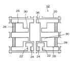
図2にリードフレーム12の平面図を示す。前記リードフレーム12は、例えば鉄合金や銅合金等の導電性を有する金属シートに井桁状の枠部20を設けるとともに、同一パターンを各枠部20の内側に形成したものである。そして前記リードは圧電発振器10の接続端子形成用リード22と実装端子形成用リード26とから構成されている。この接続端子形成用リード22と実装端子形成用リード26とは重なり合うことなく、リードフレーム12と同一面内に形成されている。前記接続端子形成用リード22は、圧電振動片18を実装する接続端子24を形成するものであり、少なくとも2つ設けられている。この接続端子形成用リード22は前記枠部20の内側端部と接続されている。そして接続端子24は圧電振動片18に設けられている接続電極32の位置に対応して設けられるとともに、導電材34を介して圧電振動片18を実装できる大きさを有している。
FIG. 2 shows a plan view of the
また前記実装端子形成用リード26は、圧電発振器10を実装基板へ実装するための端子(実装端子28)を形成するものである。この実装端子形成用リード26は前記枠部20の内側端部と接続している。そして実装端子形成用リード26は電子部品14に形成された電極に対応した位置まで延設され、その先端部に電子部品14を実装する端子(部品接続端子30)が設けられている。この部品接続端子30は、実装端子形成用リード26に切れ込みを入れることにより他の部分よりも細く形成され、他のリードに接触することなく電子部品14の前記電極に到達できるようになっている。また実装端子28は、実装端子形成用リード26の幅が広い部分に形成されるので、実装端子28と実装基板との接合強度を確保できる。
The mounting
さらに枠部20の中央部には、圧電振動片18と電子部品14との間の熱伝導を向上させるためのフレーム36が設けられている。このフレーム36は熱伝導材となり、枠部20の内側端部に接続されている。
Further, a
このような接続端子形成用リード22および実装端子形成用リード26上に、電子部品14が導電材38を介して実装される。この電子部品14は圧電振動片18を発振させるための回路であり、ICチップとなっている。この回路には、温度補償回路や電圧補償回路を付加することもできる。なお前記回路をICチップとすることなく、ディスクリートで形成してもよい。そして前記導電材38はバンプ接合材であり、電子部品14は各リード上にフリップチップボンディングされる。したがって電子部品14に設けられた前記電極と部品接続端子30と、および前記電極と接続端子24とが電気的および機械的に接続される。
The
そして電子部品14が樹脂パッケージ16の内部に封止される。すなわち電子部品14が実装されたリードフレーム12は樹脂成型金型内に載置されて、この金型内にエポキシ系等の熱硬化性樹脂を射出することにより樹脂パッケージ16が形成される。このとき、少なくとも接続端子24の主面、すなわち圧電振動片18が接続される接続面が樹脂パッケージ16から露出している。接続端子24の接続面を樹脂パッケージ16の表面に露出させるには、前記接続面を樹脂成型金型の下面に接触させた状態で樹脂を射出成型すればよい。ところで樹脂の射出圧力によって樹脂が接続端子24の接続面と樹脂成型金型との間に入り込み、樹脂が前記接続面に付着してしまう場合がある。この場合は、研磨剤入りの液体を前記接続面に向けて吹き付けて、付着した樹脂を除去すればよい。また前記接続面にレーザ光を照射して除去してもよく、薬品を塗布して除去してもよい。また実装端子形成用リード26は樹脂パッケージ16の底面にあり、樹脂パッケージ16の側方へ向けて突出している。この突出した部分に実装端子28が設けられる。なお電子部品14の上面は樹脂パッケージ16の表面に露出されてもよく(図1(b)参照)、樹脂パッケージ16の内部に封止されてもよい。
Then, the
次に、圧電振動片18が実装される側の樹脂パッケージ16表面に、モールド樹脂よりも耐湿性に優れた耐湿材40が塗布される。この耐湿材40は、接続端子24の接続面が露出されるように樹脂パッケージ16表面全体に塗布してもよく、リードの隙間からモールド樹脂が露出している箇所のみに塗布してもよい。なお、リードの隙間からモールド樹脂が露出している箇所のみだけでなく、接続端子24の周縁部をオーバーラップして耐湿材40が塗布されてもよい。この場合、耐湿材40の塗布位置が多少ずれても、モールド樹脂が露出している箇所を耐湿材40にて確実に覆うことができる。また耐湿材40は、例えばガラスが用いられ、圧電振動片18の種類によって適宜選択される。なおガラスを用いると、圧電振動片18を完全に気密封止することが可能となる。実施形態によっては、耐湿材40をパッケージに塗布しなくてもよい。なお、耐湿材40は、後で述べる圧電振動片18と接続端子24を接続するための導電材34が余分なところに流れ出すのを防止する土手の役割を担うこともできる。
Next, a moisture
この後、メッキを接続端子24の接続面および実装端子28の主面に施す。実装端子28の主面は、実装端子28を実装基板へ接合するときの実装面である。このメッキは、前記接続面と前記接続面に圧電振動片18を接合するときの導電材34と、および前記実装面と実装基板に前記実装面を接合するときの接合材との密着性を向上させるために施される。このメッキは、例えば電界メッキによりニッケルメッキや金メッキを施してもよく、また半田メッキを施してもよい。なお他の実施の形態として、メッキを前記接続面および前記実装面に施した後に、耐湿材40を樹脂パッケージ16に塗布してもよい。この場合、前記接続面の周縁部におけるメッキの表面をエッチング、研磨剤入りの液体を吹き付けて凹凸をつけておき、メッキの表面と耐湿材40との密着性を向上させるようにしてもよい。
Thereafter, plating is performed on the connection surface of the
この後、接続端子形成用リード22、実装端子形成用リード26およびフレーム36がリードフレーム12の枠部20から切断される。このとき接続端子形成用リード22およびフレーム36は、樹脂パッケージ16の外形に沿って切断されるのが好ましい。また実装端子形成用リード26は樹脂パッケージ16の外形から突出させて切断される。これにより各リードが枠部20から切断されて個々の部品にされる。
Thereafter, the connection
次に、圧電振動片18が接続端子24の接続面上に導電材34を介して実装される。図1では、圧電振動片18は片持ち状に実装されているが両持ち状に実装されてもよい。前記圧電振動片18には、厚みすべり振動を生じるATカット等の圧電振動片18を用いればよい。この圧電振動片18は、励振電極42が圧電材料からなる圧電基板48の両面に形成され、接続電極32が各励振電極42と導通して圧電基板48の角部に形成されたものである。なお圧電振動片18のかわりに、屈曲振動を生じる音叉型圧電振動片または弾性表面波を励起する弾性表面波(SAW)共振片を用いることもできる。また前記導電材34は、圧電振動片18を接続端子24に電気的および機械的に接続できるものであればよく、例えば導電性接着剤を用いることができる。
Next, the piezoelectric vibrating
この後、圧電振動片18の励振電極42の厚みをかえて、圧電発振器10の周波数調整が行われる。励振電極42の厚みの調整は、この励振電極42を削ることにより、または励振電極42に金属を成膜することにより行われる。励振電極42を削って周波数調整する場合、まず圧電振動片18が実装された樹脂パッケージ16を真空容器内に納置して、圧電振動片18を励振させる。そして励振させたときの発振周波数を計測しつつ、前記真空容器内にエッチングガスを導入してプラズマを生成し、このプラズマに励振電極42を曝してエッチングする。エッチングは所望の発振周波数に近づいたときに終了する。すなわち発振周波数をエッチングによって、ある程度追い込んでおくのである。なおプラズマを用いて励振電極42を削る場合の他に、イオンガン等でイオンを生成し、このイオンを用いてエッチングすることもできる。またレーザ光を励振電極42に照射して励振電極42を削ることもできる。ところで音叉型圧電振動片の周波数調整を行う場合は、振動腕の先端に錘が設けられているので、この錘を削ることにより周波数調整を行える。またSAW共振片の周波数調整を行う場合は、すだれ状電極(IDT)が圧電基板48表面に設けられているので、このIDTを削ることにより行われる。
Thereafter, the frequency of the
また励振電極42に金属を成膜して周波数調整する場合、マスクを励振電極42のみが露出するように圧電振動片18の上方に設け、圧電振動片18が実装された樹脂パッケージ16を成膜装置内に納置する。そして圧電振動片18を励振させて発振周波数を計測しつつ、金属を励振電極42上に成膜する。金属の成膜は所望の発振周波数に近づいたときに終了する。すなわち発振周波数を金属の成膜によって、ある程度追い込んでおくのである。なお成膜される金属材料は、励振電極42との密着性を向上させるために、励振電極42を形成する材料と同じものを用いるのが好ましい。
When adjusting the frequency by forming a metal film on the
この周波数調整後に、圧電振動片18を気密封止する蓋体44が樹脂パッケージ16に接合される。この蓋体44は金属、ガラスまたは樹脂等からなり、平面基板の周縁を立ち上げ形成した枡形状である。そして圧電振動片18が実装された樹脂パッケージ16と蓋体44とを気密容器内に納置して、気密容器内を真空にし、または窒素等の不活性ガスで充満させる。この後、蓋体44が圧電振動片18を実装した側の樹脂パッケージ16表面にロウ材を介して接合され、圧電振動片18が気密封止される。前記ロウ材は、例えば低融点ガラスや樹脂等であればよい。また耐湿材40にガラスを用いた場合は、この耐湿材40を前記ロウ材として用いることもできる。さらに蓋体44の材料に樹脂を用いた場合は、蓋体44の内面に耐湿材40を塗布してもよい。この耐湿材40は金属系であればよく、また樹脂パッケージ16表面に塗布される耐湿材40と同じものを用いてもよい。
After the frequency adjustment, the
この後、実装端子形成用リード26が折り曲げられて、実装端子28が形成される。折り曲げる方向は圧電発振器10の下方へ折り曲げられる。図1では、圧電発振器10に搭載される圧電振動片18を下方に向け、この圧電振動片18側に実装端子28が形成されている。実施の形態によっては、電子部品14を圧電発振器の下方に設け、この電子部品14側に実装端子28が形成されてもよい。
なお、実装端子形成用リード26に形成された部品接続端子30を接続端子24のように先端部分の幅を大きくしてもよい。これにより、実装端子形成用リード26と樹脂パッケージ16の接着強度を強くすることができ、実装端子形成用リード26を折り曲げる際に、実装端子形成用リード26が樹脂パッケージ16から抜けることを防ぐことができる。
Thereafter, the mounting
The
次に、圧電発振器10の発振周波数がもう一度調整される。蓋体44を封止する前工程において、励振電極42の厚みを調整して発振周波数をある程度追い込んでおいたので、本工程において圧電発振器10の発振周波数を所望の周波数に調整するのである。この調整は、電子部品14に搭載されている容量アレイの容量調整または可変容量ダイオードに供給される電圧の調整により行われる。図3に周波数調整を行う回路の説明図を示す。図3(a)は容量アレイの説明図であり、図3(b)は可変容量ダイオードを用いた回路の説明図である。なお図3(a)では、コンデンサを3つ用いた形態で記載しているが、コンデンサの数は3つに限定されることはない。図3(a)に示す容量アレイ50を用いて周波数調整する場合、容量アレイ50は電子部品14内に設けられており、容量の異なる複数のコンデンサ54が並列に接続され、これらのコンデンサ54にそれぞれスイッチ56が接続されたものである。そして電子部品14への書き込みにより、スイッチ56をON/OFFさせて負荷容量を調整し、圧電発振器10の発振周波数を所望の周波数に調整するのである。また図3(b)に示す可変容量ダイオード52を用いた回路で周波数調整する場合、この回路は電子部品14内に設けられており、可変容量ダイオード52に供給される電圧に対応して容量が調整されて、圧電発振器10の発振周波数を所望の周波数に調整するのである。このような調整は、電子部品14にプログラム等を書き込むことにより行われる。
Next, the oscillation frequency of the
このように圧電発振器10は、1枚のリードフレーム12から形成された接続端子形成用リード22上に導電材34を介して圧電振動片18を実装したので、パッケージベースを構成するセラミックの厚さ分を薄型化することができる。なお圧電振動片18をパッケージに収容した従来技術に係る圧電発振器の厚さは1.0〜1.2mmであり、パッケージベースの底板(セラミック)の厚さは0.15〜0.2mmである。したがって本実施の形態に係る圧電発振器10の厚さは、従来技術に係る圧電発振器に比べて少なくとも0.15〜0.2mm薄型化することができる。そして圧電発振器10が薄型化されたことにより、圧電振動片18と電子部品14との距離が短くなるので、圧電振動片18と電子部品14との温度差を小さくすることができる。これにより圧電発振器10を温度補償型としたときに、温度による周波数変化の補正を正確に行うことができ、周波数偏差の小さい周波数温度特性を得ることができる。
In this way, the
また圧電発振器10の周波数調整は、圧電振動片18を樹脂パッケージ16に実装した状態で、圧電振動片18に設けられた励振電極42の厚さを調整して行うことができる。そして圧電発振器10の周波数調整は、電子部品14側において負荷容量を調整して、または可変容量ダイオード52に供給される電圧を調整して行うことができる。すなわち圧電発振器10の周波数調整は、圧電振動片18の励振電極42の厚みを調整した後に、電子部品14側において負荷容量または電圧を調整する2段階の調整方法なので、電子部品14への周波数調整量を削減でき、電子部品14の小型化および圧電発振器10の小型化が可能になる。また圧電発振器10の発振周波数を細かく調整できる容量アレイ50のみ電子部品14に搭載できるので、所望の発振周波数を得ることができる。なお実施形態によっては、励振電極42の厚み調整のみで圧電発振器10の周波数調整を行ってもよい。
The frequency of the
また圧電発振器10に搭載される圧電振動片18を片持ち状に実装した場合、圧電発振器10に落下等による衝撃が加わると圧電振動片18の先端側が大きく振られ、パッケージに衝突する虞がある。この圧電振動片18が振られるのを防止するために、圧電振動片18が実装される側の樹脂パッケージ16表面に支持手段、所謂まくらを設けることができる。図4に支持手段の説明図を示す。図4は耐湿材40により支持手段58を形成した場合を示す。この支持手段58は、圧電振動片18の先端側における耐湿材40またはモールド樹脂により凸部を形成し、圧電振動片18の先端を支えればよい。またリードにより凸部を形成して支持手段58としてもよい。これにより落下等のために圧電発振器10に衝撃が加わっても、圧電振動片18が支持手段58により支えられているので大きく振られることはなく、圧電振動片18にワレやカケ等が発生することがない。したがって高信頼性の圧電発振器10を得ることができる。
Further, when the piezoelectric vibrating
上述した参考例では、熱伝導材としてリードフレーム12に設けられたフレーム36を用いた形態で説明したが、このフレーム36のかわりに熱伝導のよいシートを用いることもできる。このシートは、モールド樹脂よりも熱伝導のよい材料であればよい。そしてシートは電子部品14に貼付されてもよく、また電子部品14と圧電振動片18との間の樹脂パッケージ16に封止されて圧電発振器10に設けることもできる。なおシートが導電性の場合、実施の形態によっては圧電振動片18の励振電極42とシートとの間に容量を持つ可能性がある。この場合、非導電性の熱伝導シートを用いればよい。また実施の形態によっては、熱伝導材を用いない形態であってもよい。
In the above-described reference example, the form using the
また上述した圧電発振器10では、フリップチップボンディングにより電子部品14と接続端子24および部品接続端子30とを接続した構成であるが、ワイヤボンディングにより電子部品14と接続端子24および部品接続端子30とを接続してもよい。この場合、樹脂パッケージ16は、電子部品14およびワイヤを封止して形成されればよい。
In the
図5に調整端子を設けた圧電発振器の説明図を示す。図5(a)は平面図であり、図5(b)は同図(a)のB−B線における断面図である。上述した圧電発振器10に調整端子46を設けることもできる。この調整端子46はリードフレーム12に接続するリードによって形成され、その先端にフリップチップボンディングまたはワイヤボンディングが施されて電子部品14と接続される。なお図5はフリップチップボンディングを施した形態を示している。また接続端子形成用リードを調整端子として利用することもできる。
FIG. 5 is an explanatory diagram of a piezoelectric oscillator provided with an adjustment terminal. 5A is a plan view, and FIG. 5B is a cross-sectional view taken along the line BB in FIG. 5A. The
そして調整端子46は、電子部品14にプログラムを書き込むときに用いられる他、電子部品14の特性検査、特性調整および/または圧電振動片18と接続端子24との導通確認をするために用いられる。なお特性検査とは、モールド成型後における電子部品14の動作チェックや、圧電発振器10としての特性検査などをいう。また特性調整とは、電子部品14に温度補償回路が付加された場合に、圧電発振器10の温度による周波数変化を補正したり、入力電圧によって周波数を変化させる機能が電子部品14に付加された場合に、その変化感度を調整したりすることなどをいう。なお調整端子46は、特性検査等が行われた後に樹脂パッケージ16の外形位置で切断される。
The
図6に周波数調整用の電子部品を搭載した圧電発振器の平面図を示す。上述した実施の形態では、圧電発振器10の発振周波数は電子部品14側において負荷容量を調整して、または可変容量ダイオード52に供給される電圧を調整して行う方法について説明した。この圧電発振器の発振周波数調整の変形例として、圧電発振器にチップコンデンサ等の周波数調整用部品を搭載して調整することもできる。すなわち圧電発振器120に周波数調整用部品122を搭載するスペース124と、この周波数調整用部品122と電子部品14とを導通させるリード126とを設ければよい。前記リード126には調整用部品搭載端子128が設けられ、この端子128は樹脂パッケージ130の成型後に周波数調整用部品122を実装できるようにモールド樹脂から露出させておけばよい。この圧電発振器120の周波数調整は、まず圧電発振器120の発振周波数を測定し、この後、発振周波数の調整量に応じた容量を持つチップコンデンサを前記リード126の調整用部品搭載端子128上に実装すればよい。なお調整用部品搭載端子128は、半田等の導電材を介して調整用部品搭載端子128上に実装される。
FIG. 6 is a plan view of a piezoelectric oscillator on which electronic components for frequency adjustment are mounted. In the above-described embodiment, the method for adjusting the oscillation frequency of the
図7に樹脂パッケージ16の周縁を立ち上げ形成した圧電発振器10の断面図を示す。上述した実施形態では、圧電振動片18が実装される樹脂パッケージ16の表面は平面となっているが、図7に示すように樹脂パッケージ16の周縁を圧電振動片18側に立ち上げて側部60を形成し、圧電振動片18が実装されるキャビティ62を形成してもよい。この場合、キャビティ62を気密封止する蓋体64は平面基板とすればよい。そして蓋体64が、樹脂パッケージ16の側部60の上面にロウ材66を介して接合される。
FIG. 7 shows a cross-sectional view of the
次に、本発明の実施形態について説明する。なお参考例に係る圧電発振器と構成が同じ部分は同番号を付し、その説明を省略または簡略する。図8に第2の実施形態に係る圧電発振器の説明図を示す。図8(a)は圧電発振器の平面図であり、図8(b)は同図(a)のC−C線における断面図である。圧電発振器70は、リードフレームから形成した複数のリードの一側面に電気的に接続した電子部品14と、前記複数のリードの一部に接続されて前記電子部品側に段差を形成した複数の実装端子76と、前記複数のリードの他側面と前記複数の実装端子76の実装面とを露出させて前記電子部品14を封止したモールド材(モールド樹脂)と、前記実装端子76に接続されていない前記リードの他側面に導電材34を介して接合した圧電振動片18と、を有する構成である。
Next, an embodiment of the present invention will be described. Parts having the same configuration as those of the piezoelectric oscillator according to the reference example are denoted by the same reference numerals, and description thereof is omitted or simplified. FIG. 8 is an explanatory diagram of the piezoelectric oscillator according to the second embodiment. FIG. 8A is a plan view of the piezoelectric oscillator, and FIG. 8B is a cross-sectional view taken along the line CC in FIG. 8A. The
図9にリードフレーム72の平面図を示す。前記リードフレーム72には、接続端子形成用リード22および実装端子形成用リード74が設けられている。接続端子形成用リード22は、参考例で説明した接続端子形成用リードと同様のものである。また実装端子形成用リード74は、リードフレーム72に設けられた枠部73の内側端部から電子部品14に設けられた電極まで延設され、その先端部に幅広に形成された部品接続端子78が設けられている。この部品接続端子78のリードフレーム72側において、リードフレーム72と接続されていない部分に傾斜部80が設けられている。この傾斜部80のリードフレーム72側には、実装端子76が設けられている。そして傾斜部80は下側に折り曲げられ、この折り曲げによって部品接続端子78と実装端子76との間に上下方向の段差を生じさせている。
FIG. 9 shows a plan view of the
そして接続端子形成用リード22および実装端子形成用リード74上に導電材38を介して電子部品14が実装される。この電子部品14は、傾斜部80が折り曲げられた側に実装される。このとき電子部品14に設けられた電極と部品接続端子78と、および前記電極と接続端子24とが電気的および機械的に接続される。なお電子部品14の表面、すなわち前記電極の反対面は、実装端子76の実装面と同一平面内に位置している。この後、電子部品14の周囲がモールド樹脂で封止され、樹脂パッケージ16が形成される。このとき実装端子76の実装面および接続端子24の接続面は、樹脂パッケージ16の表面に露出させる。また実装端子76の側面を、樹脂パッケージ16の側面に露出させている。実装端子76の側面を樹脂パッケージ16の側面に露出させた場合、接合材を介して圧電発振器70が実装基板に実装されるとき、実装端子76の実装面からはみ出した前記接合材が、実装端子76の側面に沿ってせり上がり、実装基板の電極パターンから実装端子76の側面にかけてフィレットが形成される。これにより実装基板の電極パターンと圧電発振器70の実装端子76との接続を、外観から容易に確認することができる。なお実施の形態によっては、実装端子76の側面を樹脂パッケージ16の側面に露出させなくてもよい。
The
この後、圧電振動片18が実装される側の樹脂パッケージ16表面に、モールド樹脂よりも耐湿性に優れた耐湿材40が塗布される。そして接続端子24の接続面および実装端子76の実装面にメッキが施された後、接続端子形成用リード22および実装端子形成用リード74がリードフレーム72の枠部73から切断される。次に、接続端子24の接続面上に導電材34を介して圧電振動片18が実装される。そして圧電振動片18の励振電極の厚みをかえることにより周波数調整が行われた後、圧電振動片18を気密封止する蓋体44が樹脂パッケージ16に接合される。最後に、電子部品14に搭載されている容量アレイの容量調整または可変容量ダイオードに供給される電圧を調整することにより、もう一度圧電発振器70の発振周波数が調整される。
Thereafter, a moisture
このように圧電発振器70を構成することにより、第1の実施形態に係る圧電発振器10と同様の効果を奏することができる。なお上述した圧電発振器70に、第1の実施形態で説明した熱伝導材を設けてもよい。
また上述した圧電発振器70では、実装端子76の実装面と電子部品14の表面とが同一平面内にあるが、他の実施形態として、傾斜部80により形成される段差の距離を大きくして、電子部品14の表面をモールド樹脂で覆ってもよい。
By configuring the
In the
図10に接続端子を折り曲げ形成してなる圧電発振器の断面図を示す。上述した圧電発振器70では、実装端子形成用リード74に傾斜部80を設けた構成であるが、他の実施形態として、接続端子に傾斜部を設けて圧電発振器を形成してもよい。すなわち圧電発振器は、リードフレームから形成した複数のリードの一側面に電気的に接続した電子部品14と、前記複数のリードの一部に接続されて前記電子部品側に段差を形成した接続端子82と、前記複数のリードの他側面と前記接続端子82の接続面とを露出させて前記電子部品14を封止したモールド材(モールド樹脂)と、前記接続端子82の接続面に導電材を介して接合した圧電振動片18と、を有する構成である。前記段差は、リードを折り曲げた傾斜部84によって形成される。また前記接続端子82の接続面と前記電子部品14の表面とを同一面内に形成することができる。さらに電子部品14が実装されるリードの下面をハーフエッチング等により削り、このリードの下面をモールド樹脂で覆ってもよい。
FIG. 10 shows a cross-sectional view of a piezoelectric oscillator formed by bending connection terminals. In the
図11に実装端子形成用リードに段差を設けた圧電発振器の断面図を示す。図11に示すように、接続端子82を形成するリード下面が圧電発振器を実装する基板に接触させないように、実装端子形成用リード74に傾斜部84とは反対の方向に段差を形成して接続端子82を形成してもよい。したがって電子部品14が実装されるリード下面と実装端子下面とに段差を設けることができ、前記リードの下面をモールド樹脂で覆うことができる。圧電発振器が実装基板への実装される時に、不要な端子がモールド樹脂から露出していると実装基板の配線自由度がなくなるが、この形態では実装に不要な端子がモールド樹脂に覆われているので、実装基板の配線自由度を向上させることができる。
FIG. 11 shows a cross-sectional view of a piezoelectric oscillator in which a step is formed on the mounting terminal forming lead. As shown in FIG. 11, a step is formed in the mounting
図12に変形例に係る実装端子形成用リードの断面図を示す。上述した実施形態では、段差が実装端子形成用リード74または接続端子形成用リード22のいずれかを折り曲げて形成されているが、ハーフエッチングを用いて形成されてもよい。すなわちリードフレームを厚く形成しておき、エッチングによりリードフレームの上面側と下面側との厚みをかえることで、実装端子形成用リードや接続端子形成用リードを形成してもよい。実装端子形成用リード86a,86bは、図12(a),(b)に示したような形状にでき、圧電発振器の裏面に実装端子88a,88bが露出される。接続端子形成用リードも同様の形状にできる。またリードフレームを圧延することによりリードの厚みをかえて、実装端子形成用リードや接続端子形成用リードを形成してもよい。これにより圧電発振器70の幅方向の寸法を小さくすることができる。
FIG. 12 is a cross-sectional view of a mounting terminal forming lead according to a modification. In the embodiment described above, the step is formed by bending either the mounting
次に、第2の実施形態について説明する。なお参考例に係る圧電発振器と構成が同じ部分は同番号を付し、その説明を省略または簡略する。図13に第3の実施形態に係る圧電発振器の断面図を示す。圧電発振器90は、リードフレームの電子部品配置用スペースに配置して、前記リードフレームから形成した複数のリード92の一側面に電気的に接続した電子部品14と、前記複数のリード92の他側面を露出させて前記電子部品14を封止したモールド材(モールド樹脂)と、前記複数のリード92の一部に形成された接続端子93の他側面側に、導電材を介して接合した圧電振動片と、を有する構成である。また実装端子98はモールド樹脂の裏面に設けられ、このモールド樹脂を上下に貫通する穴部96に配線が設けられて(ビアホールまたはスルーホール)、実装端子98とリード92とが導通している。
Next, a second embodiment will be described. Parts having the same configuration as those of the piezoelectric oscillator according to the reference example are denoted by the same reference numerals, and description thereof is omitted or simplified. FIG. 13 shows a cross-sectional view of a piezoelectric oscillator according to the third embodiment. The piezoelectric oscillator 90 is disposed in the electronic component placement space of the lead frame and electrically connected to one side of the plurality of
図14に圧電発振器90の製造の説明図を示す。図14(a)は平面図であり、図14(b)〜(e)は断面図である。圧電発振器90の製造は次のように行われる。まず複数のリード92が形成されたリードフレームおよび電子部品14をテープシート94上に載置する。このとき電子部品14はリードフレームの電子部品配置用スペースに配置されている。そしてワイヤボンディングを電子部品14に設けられた電極とリード92とに施して電気的に接続する(図14(a),(b)参照)。なお、フリップチップボンディングにて形成してもよい。この後、電子部品14およびリード92はモールド樹脂で封止されて、樹脂パッケージ16が形成される(図14(c)参照)。このとき電子部品14とリード92とにワイヤボンディングが施された側がモールド樹脂で封止され、テープシート94が貼付されている側には樹脂パッケージ16は形成されていない。また少なくとも2つのリード92の表面から、樹脂パッケージ16を上下方向に貫通する穴部96が設けられている。この穴部96は、樹脂成型金型の内部に凸部を設けておくことにより形成される。すなわち電子部品14とリード92を樹脂成型金型に入れたときに、この金型に設けられた前記凸部の先端とリード92の表面とを接触させ、この後モールド樹脂を金型内に射出することにより穴部96が形成される。なお、貫通する穴部96は、モールド樹脂にて封止された後、レーザやエッチングにて、形成してもよい。
FIG. 14 is an explanatory diagram for manufacturing the piezoelectric oscillator 90. FIG. 14A is a plan view, and FIGS. 14B to 14E are cross-sectional views. The piezoelectric oscillator 90 is manufactured as follows. First, the lead frame on which the plurality of
この後、テープシート94が樹脂パッケージ16から剥され、樹脂パッケージ16が上下に反転される。そして圧電振動片18が、前記接続端子93に導電材34を介して実装される。また圧電振動片18が実装される側の樹脂パッケージ16表面に、耐湿材を塗布してもよい。そして圧電振動片18に設けられた励振電極の厚みをかえて周波数調整された後、圧電振動片18を気密封止する蓋体44がロウ材を介して樹脂パッケージ16に接合される(図14(d)参照)。
Thereafter, the
この後、樹脂パッケージ16に形成された穴部96と、樹脂パッケージ16(圧電発振器90)の裏面とにメッキが施されて、リード92と電気的に接続する実装端子98が樹脂パッケージ16の裏面に形成される(図14(e)参照)。なお、メッキを施す工程は、圧電振動片18が前記接続端子に実装される前に行ってもよい。
最後に、電子部品14に搭載されている容量アレイの容量調整または可変容量ダイオードに供給される電圧を調整することにより、もう一度圧電発振器90の発振周波数が調整される。このようにして圧電発振器90が製造される。
Thereafter, the
Finally, the oscillation frequency of the piezoelectric oscillator 90 is adjusted once again by adjusting the capacitance of the capacitance array mounted on the
このように圧電発振器90を構成することにより、参考例に係る圧電発振器10と同様の効果を奏することができる。なお上述した圧電発振器90に、第1の実施形態で説明した熱伝導材を設けてもよい。
また実装端子98は、樹脂パッケージ16の裏面全面を使用して形成できる。すなわち圧電発振器90の裏面は樹脂パッケージ16のみであり、電子部品14等が露出していないので、実装端子98と電子部品14とが上下に重ねて配置させることができる。したがって実装端子98を大きく形成でき、実装端子98と実装基板との間の接合強度を向上させることができる。
By configuring the piezoelectric oscillator 90 in this way, the same effects as the
The mounting
また第2の実施形態に係る圧電発振器90は、樹脂パッケージ16を上下方向に貫通して実装端子98とリード92とが導通しているので、リードフレームを折り曲げて実装端子98と電子部品14とを導通させる場合に比べて、リードフレームを折り曲げる分を小型化することができる。
In the piezoelectric oscillator 90 according to the second embodiment , since the mounting
図15に圧電発振器を製造する他の実施形態の説明図を示す。第3の実施形態に係る圧電発振器90を平面方向に複数並べて形成し、ダイシングにより個別化して製造することもできる。なおダイシングする位置は、図15において二点鎖線で示している。この場合、樹脂パッケージ16に穴部96(スルーホールまたはビアホール)を設けてリード92と実装端子98とを導通させる実施形態の他に、樹脂パッケージ16の側面にキャスタレーションを設けてリード92と実装端子98とを導通させてもよい。また、この実施形態では、圧電振動片を樹脂パッケージに実装する前に実装端子98を形成している。
なお、第3の実施形態に係る圧電発振器90において、実装端子と接続端子を反対に形成してもよい。つまり、実装端子98はリード92により形成し、接続端子はリード92と穴部を介して接続して形成してもよい。
FIG. 15 is an explanatory view of another embodiment for manufacturing a piezoelectric oscillator. A plurality of piezoelectric oscillators 90 according to the third embodiment may be formed side by side in the plane direction, and may be manufactured individually by dicing. The dicing position is indicated by a two-dot chain line in FIG. In this case, in addition to the embodiment in which the hole 96 (through hole or via hole) is provided in the
In the piezoelectric oscillator 90 according to the third embodiment, the mounting terminal and the connection terminal may be formed in the opposite manner. That is, the mounting
次に、第3の実施形態について説明する。第3の実施形態では、第1〜第3の実施形態で説明した圧電発振器10,70,90を電子機器に搭載した一例について説明する。図16にディジタル式携帯電話の概略構成図を示す。ディジタル式携帯電話100は、送受信信号の送信部102および受信部104等を有し、この送信部102および受信部104に、これらを制御する中央演算装置(CPU)106が接続されている。またCPU106は、送受信信号の変調および復調の他に表示部や情報入力のための操作キー等からなる情報の入出力部108や、RAM,ROM等からなるメモリ110の制御を行っている。このためCPU106には圧電デバイス112が取付けられ、その出力周波数をCPU106に内蔵された所定の分周回路(不図示)等により、制御内容に適合したクロック信号として利用するようにされている。
Next, a third embodiment will be described. In the third embodiment , an example in which the
本発明の実施形態に係る圧電発振器10,70,90が応用されるものとして、例えば温度補償型水晶発振器(TCXO)がある。このTCXOは、周囲の温度変化による周波数変動を小さくした圧電発振器であって、受信部や送信部の周波数基準源として広く利用されている。このTCXOは、近年の携帯電話装置の小型化に伴い、小型化への要求が高くなっており、本発明の実施形態に係る圧電発振器の小型化は極めて有用である。また、本発明の実施形態に係る圧電発振器は、例えばCPUを含む携帯電話装置に日付時刻情報を供給するリアルタイムクロックにも応用することができる。
For example, a temperature-compensated crystal oscillator (TCXO) is applied to the
また本発明の実施形態に係る圧電発振器10,70,90は、上記のディジタル式携帯電話装置に限らず、パーソナルコンピュータ、ワークステーション、PDA(Personal Digital[Data] Assistants:携帯情報端末)等の、圧電発振器により制御用のクロック信号を得る電子機器に適用することができる。このように、上述した実施形態に係る圧電発振器を電子機器に利用することにより、より小型で信頼性の高い電子機器を実現することができる。
Further, the
10………圧電発振器、14………電子部品、16………樹脂パッケージ、18………圧電振動片、24………接続端子、28………実装端子、70………圧電発振器、76………実装端子、90………圧電発振器、98………実装端子、100………ディジタル式携帯電話。
10 ......... Piezoelectric oscillator, 14 ......... Electronic components, 16 ... …… Resin package, 18 ......... Piezoelectric vibrating piece, 24 ......... Connecting terminal, 28 ......... Mounting terminal, 70 ......... Piezoelectric oscillator, 76... Mounting terminal, 90... Piezoelectric oscillator, 98... Mounting terminal, 100.
Claims (9)
前記複数のリードの一部に接続されて前記電子部品側に折り曲げて部品接続端子との間に段差を形成した複数の実装端子と、
前記複数のリードの他側面と前記複数の実装端子の実装面とを露出させて前記電子部品を封止したモールド材と、
前記リードの他側面に導電材を介して接合した圧電振動片と、
を有することを特徴とする圧電発振器。 An electronic component electrically connected to one side of a plurality of leads formed from a lead frame;
A plurality of mounting terminals connected to a part of the plurality of leads and bent to the electronic component side to form a step between the component connection terminals ;
A molding material that seals the electronic component by exposing the other side surfaces of the plurality of leads and the mounting surfaces of the plurality of mounting terminals;
A piezoelectric vibrating piece joined to the other side of the lead via a conductive material;
A piezoelectric oscillator comprising:
前記複数のリードの一部に接続されて前記電子部品が実装されるリード面との間に段差を形成した接続端子と、
前記複数のリードの他側面と前記接続端子の接続面とを露出させて前記電子部品を封止したモールド材と、
前記接続端子の接続面に導電材を介して接合した圧電振動片と、
を有することを特徴とする圧電発振器。 An electronic component electrically connected to one side of a plurality of leads formed from a lead frame;
A connection terminal that is connected to a part of the plurality of leads to form a step between the lead surface on which the electronic component is mounted ;
A molding material that seals the electronic component by exposing the other side surface of the plurality of leads and the connection surface of the connection terminal;
A piezoelectric vibrating piece joined to a connection surface of the connection terminal via a conductive material;
A piezoelectric oscillator comprising:
前記複数のリードの他側面を露出させて前記電子部品を封止したモールド材と、
前記複数のリードの他側面に、導電材を介して接合した圧電振動片と、
前記モールド材の一部に穴部が設けられ、前記穴部に形成された配線を介して前記リードと電気的に接続された実装端子と、
を有することを特徴とする圧電発振器。 An electronic component electrically connected to one side of a plurality of leads formed from a lead frame;
A molding material that seals the electronic component by exposing the other side of the leads; and
A piezoelectric vibrating piece joined to the other side of the plurality of leads via a conductive material;
A hole is provided in a part of the mold material, and a mounting terminal electrically connected to the lead via a wiring formed in the hole,
A piezoelectric oscillator comprising:
Priority Applications (2)
| Application Number | Priority Date | Filing Date | Title |
|---|---|---|---|
| JP2004158519A JP4238779B2 (en) | 2004-05-28 | 2004-05-28 | Piezoelectric oscillator and electronic equipment |
| US11/138,288 US20050264140A1 (en) | 2004-05-28 | 2005-05-27 | Piezoelectric oscillator and electronic device |
Applications Claiming Priority (1)
| Application Number | Priority Date | Filing Date | Title |
|---|---|---|---|
| JP2004158519A JP4238779B2 (en) | 2004-05-28 | 2004-05-28 | Piezoelectric oscillator and electronic equipment |
Publications (2)
| Publication Number | Publication Date |
|---|---|
| JP2005341326A JP2005341326A (en) | 2005-12-08 |
| JP4238779B2 true JP4238779B2 (en) | 2009-03-18 |
Family
ID=35424413
Family Applications (1)
| Application Number | Title | Priority Date | Filing Date |
|---|---|---|---|
| JP2004158519A Expired - Fee Related JP4238779B2 (en) | 2004-05-28 | 2004-05-28 | Piezoelectric oscillator and electronic equipment |
Country Status (2)
| Country | Link |
|---|---|
| US (1) | US20050264140A1 (en) |
| JP (1) | JP4238779B2 (en) |
Families Citing this family (14)
| Publication number | Priority date | Publication date | Assignee | Title |
|---|---|---|---|---|
| US7694734B2 (en) * | 2005-10-31 | 2010-04-13 | Baker Hughes Incorporated | Method and apparatus for insulating a resonator downhole |
| WO2007147137A2 (en) | 2006-06-15 | 2007-12-21 | Sitime Corporation | Stacked die package for mems resonator system |
| JP5111018B2 (en) * | 2007-08-27 | 2012-12-26 | セイコーインスツル株式会社 | Airtight terminal manufacturing method and piezoelectric vibrator manufacturing method |
| US8256288B2 (en) | 2008-12-16 | 2012-09-04 | Seiko Epson Corporation | Sensor device |
| JP5360371B2 (en) * | 2008-12-16 | 2013-12-04 | セイコーエプソン株式会社 | Electronic devices |
| DE102010039599A1 (en) * | 2010-08-20 | 2012-02-23 | Robert Bosch Gmbh | Sensor module for receiving a pressure sensor chip and for mounting in a sensor housing |
| KR20130020331A (en) * | 2011-08-19 | 2013-02-27 | 삼성전기주식회사 | Ultrasonic sensor |
| US9230890B2 (en) | 2012-04-27 | 2016-01-05 | Lapis Semiconductor Co., Ltd. | Semiconductor device and measurement device |
| US9754803B2 (en) * | 2013-03-27 | 2017-09-05 | Seiko Epson Corporation | Electronic device, electronic apparatus, moving object, and method for manufacturing electronic device |
| JP6340754B2 (en) * | 2013-03-29 | 2018-06-13 | セイコーエプソン株式会社 | Electronic device, electronic apparatus, moving object, and method for manufacturing electronic device |
| JP2014207313A (en) * | 2013-04-12 | 2014-10-30 | セイコーエプソン株式会社 | Electronic component, electronic apparatus and mobile |
| JP5582323B2 (en) * | 2013-04-22 | 2014-09-03 | セイコーエプソン株式会社 | Electronic devices |
| JP6276338B2 (en) * | 2016-07-25 | 2018-02-07 | ラピスセミコンダクタ株式会社 | Semiconductor device and measuring instrument |
| JP7552285B2 (en) * | 2020-11-24 | 2024-09-18 | セイコーエプソン株式会社 | Oscillator and manufacturing method |
Family Cites Families (6)
| Publication number | Priority date | Publication date | Assignee | Title |
|---|---|---|---|---|
| US6456168B1 (en) * | 2000-12-29 | 2002-09-24 | Cts Corporation | Temperature compensated crystal oscillator assembled on crystal base |
| US6759913B2 (en) * | 2001-06-29 | 2004-07-06 | Cts Corporation | Crystal resonator based oscillator formed by attaching two separate housings |
| DE10238523B4 (en) * | 2002-08-22 | 2014-10-02 | Epcos Ag | Encapsulated electronic component and method of manufacture |
| JP3918794B2 (en) * | 2002-12-10 | 2007-05-23 | セイコーエプソン株式会社 | Piezoelectric oscillator, manufacturing method thereof, and electronic apparatus |
| JP3783235B2 (en) * | 2003-06-16 | 2006-06-07 | セイコーエプソン株式会社 | Piezoelectric oscillator, manufacturing method thereof, mobile phone device using piezoelectric oscillator, and electronic device using piezoelectric oscillator |
| JP2006311380A (en) * | 2005-04-28 | 2006-11-09 | Epson Toyocom Corp | Piezoelectric vibrator and piezoelectric oscillator |
-
2004
- 2004-05-28 JP JP2004158519A patent/JP4238779B2/en not_active Expired - Fee Related
-
2005
- 2005-05-27 US US11/138,288 patent/US20050264140A1/en not_active Abandoned
Also Published As
| Publication number | Publication date |
|---|---|
| US20050264140A1 (en) | 2005-12-01 |
| JP2005341326A (en) | 2005-12-08 |
Similar Documents
| Publication | Publication Date | Title |
|---|---|---|
| JP4222147B2 (en) | Piezoelectric oscillator, mobile phone device using piezoelectric oscillator, and electronic device using piezoelectric oscillator | |
| JP4238779B2 (en) | Piezoelectric oscillator and electronic equipment | |
| EP2012427A2 (en) | Piezoelectric vibrating pieces and piezoelectric devices | |
| JP2002335128A (en) | Piezo device | |
| JP2006279872A (en) | Piezoelectric vibrator, manufacturing method thereof, and manufacturing method of piezoelectric oscillator using the piezoelectric vibrator | |
| EP2355341A2 (en) | Piezoelectric vibrator and oscillator using the same | |
| JP2009188483A (en) | Piezoelectric device and surface mount piezoelectric oscillator | |
| US7872401B2 (en) | Piezoelectric vibrator with hermetically closed casing and filler comprising non-spherical conductive particles | |
| US8281468B2 (en) | Method of manufacturing piezoelectric vibrators | |
| JP4692715B2 (en) | Piezoelectric oscillator, electronic device, and method for manufacturing piezoelectric oscillator | |
| JP2002353766A (en) | Piezo device | |
| JPWO2010097905A1 (en) | Package manufacturing method, piezoelectric vibrator, oscillator, electronic device, and radio timepiece | |
| JP5258957B2 (en) | Piezoelectric vibrator manufacturing method and substrate manufacturing method | |
| JPH11186850A (en) | Piezoelectric oscillator | |
| JP2009194789A (en) | Method of manufacturing piezoelectric vibrator, the piezoelectric vibrator, oscillator, electronic equipment, and radio-controlled clock | |
| JP4437694B2 (en) | Piezoelectric oscillator manufacturing method, piezoelectric oscillator, and electronic device | |
| JP2002280865A (en) | Piezo device | |
| JP2010124494A (en) | Piezoelectric oscillator, electronic apparatus and method of manufacturing piezoelectric oscillator | |
| JP4457760B2 (en) | Piezoelectric oscillator and electronic equipment | |
| JP4472445B2 (en) | Method for manufacturing piezoelectric oscillator | |
| JP2006101181A (en) | Piezoelectric oscillator and electronic equipment | |
| JP2005094461A (en) | Piezoelectric device, manufacturing method thereof, mobile phone device using piezoelectric device, and electronic apparatus using piezoelectric device | |
| JP2006101090A (en) | Method for adjusting frequency of piezoelectric oscillator, piezoelectric oscillator and electronic device | |
| JP2005260727A (en) | Piezo oscillating element supporting structure, and piezo oscillator | |
| JP2006101241A (en) | Piezoelectric oscillator and manufacturing method thereof |
Legal Events
| Date | Code | Title | Description |
|---|---|---|---|
| A621 | Written request for application examination |
Free format text: JAPANESE INTERMEDIATE CODE: A621 Effective date: 20051104 |
|
| A977 | Report on retrieval |
Free format text: JAPANESE INTERMEDIATE CODE: A971007 Effective date: 20080225 |
|
| A131 | Notification of reasons for refusal |
Free format text: JAPANESE INTERMEDIATE CODE: A131 Effective date: 20080417 |
|
| A521 | Request for written amendment filed |
Free format text: JAPANESE INTERMEDIATE CODE: A523 Effective date: 20080603 |
|
| TRDD | Decision of grant or rejection written | ||
| A01 | Written decision to grant a patent or to grant a registration (utility model) |
Free format text: JAPANESE INTERMEDIATE CODE: A01 Effective date: 20081125 |
|
| A01 | Written decision to grant a patent or to grant a registration (utility model) |
Free format text: JAPANESE INTERMEDIATE CODE: A01 |
|
| A61 | First payment of annual fees (during grant procedure) |
Free format text: JAPANESE INTERMEDIATE CODE: A61 Effective date: 20081208 |
|
| FPAY | Renewal fee payment (event date is renewal date of database) |
Free format text: PAYMENT UNTIL: 20120109 Year of fee payment: 3 |
|
| R150 | Certificate of patent or registration of utility model |
Free format text: JAPANESE INTERMEDIATE CODE: R150 |
|
| FPAY | Renewal fee payment (event date is renewal date of database) |
Free format text: PAYMENT UNTIL: 20120109 Year of fee payment: 3 |
|
| FPAY | Renewal fee payment (event date is renewal date of database) |
Free format text: PAYMENT UNTIL: 20130109 Year of fee payment: 4 |
|
| FPAY | Renewal fee payment (event date is renewal date of database) |
Free format text: PAYMENT UNTIL: 20130109 Year of fee payment: 4 |
|
| FPAY | Renewal fee payment (event date is renewal date of database) |
Free format text: PAYMENT UNTIL: 20140109 Year of fee payment: 5 |
|
| S531 | Written request for registration of change of domicile |
Free format text: JAPANESE INTERMEDIATE CODE: R313531 |
|
| R350 | Written notification of registration of transfer |
Free format text: JAPANESE INTERMEDIATE CODE: R350 |
|
| LAPS | Cancellation because of no payment of annual fees |