JP2004170917A - 電気光学装置及び電子機器 - Google Patents
電気光学装置及び電子機器 Download PDFInfo
- Publication number
- JP2004170917A JP2004170917A JP2003321789A JP2003321789A JP2004170917A JP 2004170917 A JP2004170917 A JP 2004170917A JP 2003321789 A JP2003321789 A JP 2003321789A JP 2003321789 A JP2003321789 A JP 2003321789A JP 2004170917 A JP2004170917 A JP 2004170917A
- Authority
- JP
- Japan
- Prior art keywords
- data line
- electro
- film
- optical device
- layer
- Prior art date
- Legal status (The legal status is an assumption and is not a legal conclusion. Google has not performed a legal analysis and makes no representation as to the accuracy of the status listed.)
- Granted
Links
- 239000010410 layer Substances 0.000 claims abstract description 355
- 150000004767 nitrides Chemical class 0.000 claims abstract description 133
- 239000000758 substrate Substances 0.000 claims abstract description 112
- 239000003990 capacitor Substances 0.000 claims abstract description 101
- 238000003860 storage Methods 0.000 claims abstract description 58
- 239000011229 interlayer Substances 0.000 claims abstract description 52
- 239000010408 film Substances 0.000 claims description 424
- 239000000463 material Substances 0.000 claims description 32
- 239000010409 thin film Substances 0.000 claims description 29
- 229910052782 aluminium Inorganic materials 0.000 claims description 26
- XAGFODPZIPBFFR-UHFFFAOYSA-N aluminium Chemical compound [Al] XAGFODPZIPBFFR-UHFFFAOYSA-N 0.000 claims description 26
- 238000000034 method Methods 0.000 claims description 25
- 229910021420 polycrystalline silicon Inorganic materials 0.000 claims description 21
- 229920005591 polysilicon Polymers 0.000 claims description 21
- 230000008569 process Effects 0.000 claims description 16
- 239000004020 conductor Substances 0.000 claims description 10
- 239000007787 solid Substances 0.000 claims description 9
- 230000000694 effects Effects 0.000 abstract description 34
- 230000008878 coupling Effects 0.000 abstract description 23
- 238000010168 coupling process Methods 0.000 abstract description 23
- 238000005859 coupling reaction Methods 0.000 abstract description 23
- 238000010586 diagram Methods 0.000 abstract description 6
- 239000004065 semiconductor Substances 0.000 description 35
- 239000004973 liquid crystal related substance Substances 0.000 description 31
- 230000006870 function Effects 0.000 description 20
- 229910052814 silicon oxide Inorganic materials 0.000 description 19
- 229910052581 Si3N4 Inorganic materials 0.000 description 17
- VYPSYNLAJGMNEJ-UHFFFAOYSA-N Silicium dioxide Chemical compound O=[Si]=O VYPSYNLAJGMNEJ-UHFFFAOYSA-N 0.000 description 17
- 238000004519 manufacturing process Methods 0.000 description 17
- HQVNEWCFYHHQES-UHFFFAOYSA-N silicon nitride Chemical compound N12[Si]34N5[Si]62N3[Si]51N64 HQVNEWCFYHHQES-UHFFFAOYSA-N 0.000 description 17
- 238000000059 patterning Methods 0.000 description 15
- 238000005530 etching Methods 0.000 description 14
- NRTOMJZYCJJWKI-UHFFFAOYSA-N Titanium nitride Chemical compound [Ti]#N NRTOMJZYCJJWKI-UHFFFAOYSA-N 0.000 description 13
- 238000002834 transmittance Methods 0.000 description 13
- 229910052751 metal Inorganic materials 0.000 description 11
- 239000002184 metal Substances 0.000 description 11
- 230000003405 preventing effect Effects 0.000 description 11
- 239000011159 matrix material Substances 0.000 description 10
- 239000005368 silicate glass Substances 0.000 description 9
- 230000007797 corrosion Effects 0.000 description 8
- 238000005260 corrosion Methods 0.000 description 8
- 230000035515 penetration Effects 0.000 description 7
- 229910045601 alloy Inorganic materials 0.000 description 6
- 239000000956 alloy Substances 0.000 description 6
- 230000015572 biosynthetic process Effects 0.000 description 6
- 239000005380 borophosphosilicate glass Substances 0.000 description 6
- 230000008859 change Effects 0.000 description 6
- 230000005684 electric field Effects 0.000 description 6
- 239000003566 sealing material Substances 0.000 description 6
- 230000006378 damage Effects 0.000 description 5
- 230000007547 defect Effects 0.000 description 5
- 238000009792 diffusion process Methods 0.000 description 5
- 239000011347 resin Substances 0.000 description 5
- 229920005989 resin Polymers 0.000 description 5
- XLYOFNOQVPJJNP-UHFFFAOYSA-N water Substances O XLYOFNOQVPJJNP-UHFFFAOYSA-N 0.000 description 5
- XUIMIQQOPSSXEZ-UHFFFAOYSA-N Silicon Chemical compound [Si] XUIMIQQOPSSXEZ-UHFFFAOYSA-N 0.000 description 4
- 230000005540 biological transmission Effects 0.000 description 4
- 239000011651 chromium Substances 0.000 description 4
- 239000013078 crystal Substances 0.000 description 4
- 230000007423 decrease Effects 0.000 description 4
- 239000011521 glass Substances 0.000 description 4
- 230000008595 infiltration Effects 0.000 description 4
- 238000001764 infiltration Methods 0.000 description 4
- 238000009413 insulation Methods 0.000 description 4
- 239000002243 precursor Substances 0.000 description 4
- 229910052710 silicon Inorganic materials 0.000 description 4
- 239000010703 silicon Substances 0.000 description 4
- 239000010936 titanium Substances 0.000 description 4
- 230000000903 blocking effect Effects 0.000 description 3
- 229910052804 chromium Inorganic materials 0.000 description 3
- 230000004048 modification Effects 0.000 description 3
- 238000012986 modification Methods 0.000 description 3
- 229910052750 molybdenum Inorganic materials 0.000 description 3
- 238000000206 photolithography Methods 0.000 description 3
- 238000005498 polishing Methods 0.000 description 3
- 239000003870 refractory metal Substances 0.000 description 3
- 229910021332 silicide Inorganic materials 0.000 description 3
- FVBUAEGBCNSCDD-UHFFFAOYSA-N silicide(4-) Chemical compound [Si-4] FVBUAEGBCNSCDD-UHFFFAOYSA-N 0.000 description 3
- 229910052715 tantalum Inorganic materials 0.000 description 3
- 229910052719 titanium Inorganic materials 0.000 description 3
- 229910052721 tungsten Inorganic materials 0.000 description 3
- 239000004988 Nematic liquid crystal Substances 0.000 description 2
- 229910003070 TaOx Inorganic materials 0.000 description 2
- 229910010413 TiO 2 Inorganic materials 0.000 description 2
- ATJFFYVFTNAWJD-UHFFFAOYSA-N Tin Chemical compound [Sn] ATJFFYVFTNAWJD-UHFFFAOYSA-N 0.000 description 2
- RTAQQCXQSZGOHL-UHFFFAOYSA-N Titanium Chemical compound [Ti] RTAQQCXQSZGOHL-UHFFFAOYSA-N 0.000 description 2
- 230000009471 action Effects 0.000 description 2
- PNEYBMLMFCGWSK-UHFFFAOYSA-N aluminium oxide Inorganic materials [O-2].[O-2].[O-2].[Al+3].[Al+3] PNEYBMLMFCGWSK-UHFFFAOYSA-N 0.000 description 2
- 230000004888 barrier function Effects 0.000 description 2
- 239000011324 bead Substances 0.000 description 2
- 238000006243 chemical reaction Methods 0.000 description 2
- 239000003086 colorant Substances 0.000 description 2
- 238000010292 electrical insulation Methods 0.000 description 2
- 238000005401 electroluminescence Methods 0.000 description 2
- 230000003628 erosive effect Effects 0.000 description 2
- 239000003365 glass fiber Substances 0.000 description 2
- 230000006872 improvement Effects 0.000 description 2
- 239000012535 impurity Substances 0.000 description 2
- AMGQUBHHOARCQH-UHFFFAOYSA-N indium;oxotin Chemical compound [In].[Sn]=O AMGQUBHHOARCQH-UHFFFAOYSA-N 0.000 description 2
- 238000010030 laminating Methods 0.000 description 2
- 230000031700 light absorption Effects 0.000 description 2
- 230000003287 optical effect Effects 0.000 description 2
- 230000002093 peripheral effect Effects 0.000 description 2
- 239000010453 quartz Substances 0.000 description 2
- 230000009467 reduction Effects 0.000 description 2
- 125000006850 spacer group Chemical group 0.000 description 2
- 239000000126 substance Substances 0.000 description 2
- 229920001187 thermosetting polymer Polymers 0.000 description 2
- 229910000838 Al alloy Inorganic materials 0.000 description 1
- ZOXJGFHDIHLPTG-UHFFFAOYSA-N Boron Chemical compound [B] ZOXJGFHDIHLPTG-UHFFFAOYSA-N 0.000 description 1
- VYZAMTAEIAYCRO-UHFFFAOYSA-N Chromium Chemical compound [Cr] VYZAMTAEIAYCRO-UHFFFAOYSA-N 0.000 description 1
- UFHFLCQGNIYNRP-UHFFFAOYSA-N Hydrogen Chemical compound [H][H] UFHFLCQGNIYNRP-UHFFFAOYSA-N 0.000 description 1
- ZOKXTWBITQBERF-UHFFFAOYSA-N Molybdenum Chemical compound [Mo] ZOKXTWBITQBERF-UHFFFAOYSA-N 0.000 description 1
- OAICVXFJPJFONN-UHFFFAOYSA-N Phosphorus Chemical compound [P] OAICVXFJPJFONN-UHFFFAOYSA-N 0.000 description 1
- 229910004298 SiO 2 Inorganic materials 0.000 description 1
- GWEVSGVZZGPLCZ-UHFFFAOYSA-N Titan oxide Chemical compound O=[Ti]=O GWEVSGVZZGPLCZ-UHFFFAOYSA-N 0.000 description 1
- GDFCWFBWQUEQIJ-UHFFFAOYSA-N [B].[P] Chemical compound [B].[P] GDFCWFBWQUEQIJ-UHFFFAOYSA-N 0.000 description 1
- WOIHABYNKOEWFG-UHFFFAOYSA-N [Sr].[Ba] Chemical compound [Sr].[Ba] WOIHABYNKOEWFG-UHFFFAOYSA-N 0.000 description 1
- 239000000853 adhesive Substances 0.000 description 1
- 230000001070 adhesive effect Effects 0.000 description 1
- 230000002411 adverse Effects 0.000 description 1
- 229910002113 barium titanate Inorganic materials 0.000 description 1
- 230000008901 benefit Effects 0.000 description 1
- 229910052796 boron Inorganic materials 0.000 description 1
- 230000015556 catabolic process Effects 0.000 description 1
- 238000004140 cleaning Methods 0.000 description 1
- 239000011248 coating agent Substances 0.000 description 1
- 238000000576 coating method Methods 0.000 description 1
- 230000000295 complement effect Effects 0.000 description 1
- 238000012790 confirmation Methods 0.000 description 1
- 238000013016 damping Methods 0.000 description 1
- 230000002950 deficient Effects 0.000 description 1
- 230000006866 deterioration Effects 0.000 description 1
- 230000002542 deteriorative effect Effects 0.000 description 1
- 238000001312 dry etching Methods 0.000 description 1
- 230000009977 dual effect Effects 0.000 description 1
- 238000001962 electrophoresis Methods 0.000 description 1
- 230000001747 exhibiting effect Effects 0.000 description 1
- 238000010304 firing Methods 0.000 description 1
- 229910000449 hafnium oxide Inorganic materials 0.000 description 1
- WIHZLLGSGQNAGK-UHFFFAOYSA-N hafnium(4+);oxygen(2-) Chemical compound [O-2].[O-2].[Hf+4] WIHZLLGSGQNAGK-UHFFFAOYSA-N 0.000 description 1
- 238000010438 heat treatment Methods 0.000 description 1
- 229910052739 hydrogen Inorganic materials 0.000 description 1
- 239000001257 hydrogen Substances 0.000 description 1
- 238000005984 hydrogenation reaction Methods 0.000 description 1
- 238000007689 inspection Methods 0.000 description 1
- 150000002500 ions Chemical class 0.000 description 1
- 230000007774 longterm Effects 0.000 description 1
- 229910001507 metal halide Inorganic materials 0.000 description 1
- 150000005309 metal halides Chemical class 0.000 description 1
- 238000002156 mixing Methods 0.000 description 1
- 239000011733 molybdenum Substances 0.000 description 1
- BPUBBGLMJRNUCC-UHFFFAOYSA-N oxygen(2-);tantalum(5+) Chemical compound [O-2].[O-2].[O-2].[O-2].[O-2].[Ta+5].[Ta+5] BPUBBGLMJRNUCC-UHFFFAOYSA-N 0.000 description 1
- RVTZCBVAJQQJTK-UHFFFAOYSA-N oxygen(2-);zirconium(4+) Chemical compound [O-2].[O-2].[Zr+4] RVTZCBVAJQQJTK-UHFFFAOYSA-N 0.000 description 1
- 230000000149 penetrating effect Effects 0.000 description 1
- 229910052698 phosphorus Inorganic materials 0.000 description 1
- 239000011574 phosphorus Substances 0.000 description 1
- 238000000016 photochemical curing Methods 0.000 description 1
- 238000005268 plasma chemical vapour deposition Methods 0.000 description 1
- 229920001721 polyimide Polymers 0.000 description 1
- 230000002265 prevention Effects 0.000 description 1
- 230000002035 prolonged effect Effects 0.000 description 1
- 238000005070 sampling Methods 0.000 description 1
- 238000007789 sealing Methods 0.000 description 1
- 239000002356 single layer Substances 0.000 description 1
- GUVRBAGPIYLISA-UHFFFAOYSA-N tantalum atom Chemical compound [Ta] GUVRBAGPIYLISA-UHFFFAOYSA-N 0.000 description 1
- 229910001936 tantalum oxide Inorganic materials 0.000 description 1
- OGIDPMRJRNCKJF-UHFFFAOYSA-N titanium oxide Inorganic materials [Ti]=O OGIDPMRJRNCKJF-UHFFFAOYSA-N 0.000 description 1
- WFKWXMTUELFFGS-UHFFFAOYSA-N tungsten Chemical compound [W] WFKWXMTUELFFGS-UHFFFAOYSA-N 0.000 description 1
- 239000010937 tungsten Substances 0.000 description 1
- YVTHLONGBIQYBO-UHFFFAOYSA-N zinc indium(3+) oxygen(2-) Chemical compound [O--].[Zn++].[In+3] YVTHLONGBIQYBO-UHFFFAOYSA-N 0.000 description 1
- 229910001928 zirconium oxide Inorganic materials 0.000 description 1
Images


Classifications
-
- G—PHYSICS
- G02—OPTICS
- G02F—OPTICAL DEVICES OR ARRANGEMENTS FOR THE CONTROL OF LIGHT BY MODIFICATION OF THE OPTICAL PROPERTIES OF THE MEDIA OF THE ELEMENTS INVOLVED THEREIN; NON-LINEAR OPTICS; FREQUENCY-CHANGING OF LIGHT; OPTICAL LOGIC ELEMENTS; OPTICAL ANALOGUE/DIGITAL CONVERTERS
- G02F1/00—Devices or arrangements for the control of the intensity, colour, phase, polarisation or direction of light arriving from an independent light source, e.g. switching, gating or modulating; Non-linear optics
- G02F1/01—Devices or arrangements for the control of the intensity, colour, phase, polarisation or direction of light arriving from an independent light source, e.g. switching, gating or modulating; Non-linear optics for the control of the intensity, phase, polarisation or colour
- G02F1/13—Devices or arrangements for the control of the intensity, colour, phase, polarisation or direction of light arriving from an independent light source, e.g. switching, gating or modulating; Non-linear optics for the control of the intensity, phase, polarisation or colour based on liquid crystals, e.g. single liquid crystal display cells
- G02F1/133—Constructional arrangements; Operation of liquid crystal cells; Circuit arrangements
- G02F1/136—Liquid crystal cells structurally associated with a semi-conducting layer or substrate, e.g. cells forming part of an integrated circuit
- G02F1/1362—Active matrix addressed cells
-
- G—PHYSICS
- G02—OPTICS
- G02F—OPTICAL DEVICES OR ARRANGEMENTS FOR THE CONTROL OF LIGHT BY MODIFICATION OF THE OPTICAL PROPERTIES OF THE MEDIA OF THE ELEMENTS INVOLVED THEREIN; NON-LINEAR OPTICS; FREQUENCY-CHANGING OF LIGHT; OPTICAL LOGIC ELEMENTS; OPTICAL ANALOGUE/DIGITAL CONVERTERS
- G02F1/00—Devices or arrangements for the control of the intensity, colour, phase, polarisation or direction of light arriving from an independent light source, e.g. switching, gating or modulating; Non-linear optics
- G02F1/01—Devices or arrangements for the control of the intensity, colour, phase, polarisation or direction of light arriving from an independent light source, e.g. switching, gating or modulating; Non-linear optics for the control of the intensity, phase, polarisation or colour
- G02F1/13—Devices or arrangements for the control of the intensity, colour, phase, polarisation or direction of light arriving from an independent light source, e.g. switching, gating or modulating; Non-linear optics for the control of the intensity, phase, polarisation or colour based on liquid crystals, e.g. single liquid crystal display cells
- G02F1/133—Constructional arrangements; Operation of liquid crystal cells; Circuit arrangements
- G02F1/136—Liquid crystal cells structurally associated with a semi-conducting layer or substrate, e.g. cells forming part of an integrated circuit
- G02F1/1362—Active matrix addressed cells
- G02F1/136218—Shield electrodes
Landscapes
- Physics & Mathematics (AREA)
- Nonlinear Science (AREA)
- Engineering & Computer Science (AREA)
- Microelectronics & Electronic Packaging (AREA)
- Mathematical Physics (AREA)
- Chemical & Material Sciences (AREA)
- Crystallography & Structural Chemistry (AREA)
- General Physics & Mathematics (AREA)
- Optics & Photonics (AREA)
- Liquid Crystal (AREA)
- Devices For Indicating Variable Information By Combining Individual Elements (AREA)
- Thin Film Transistor (AREA)
Abstract
【解決手段】 基板上に、データ線(6a)、走査線(3a)、画素電極(9a)及びTFT(30)が積層構造の一部をなして備えられている。この基板上には更に、TFT及び画素電極に電気的に接続された蓄積容量(70)と、データ線及び画素電極間に配置されたシールド層(400)と、前記画素電極の下地として配置された層間絶縁膜(43)とが、前記積層構造の一部をなして備えられている。このうちシールド層は窒化膜を含む。
【選択図】 図4
Description
すなわち、前述のような電気光学装置では、画素電極及びデータ線を、比較的狭い領域内で平面的に、あるいは立体的に、近接させて形成する場合も生じるが、このような場合、両者間に容量カップリングを生じさせるおそれがあった。つまり、いったん電圧が印加されれば、所定の期間中、本来一定であるべき画素電極の電位が、それに近接するデータ線に対する通電によって変化する可能性があるのである。これにより、画像上にはデータ線に沿うような帯状の表示ムラが生じるおそれがある。
また、第二に、前記シールド層は、前記データ線に沿い、かつ、前記データ線よりも幅広に形成されている。
この構成によれば、本発明に係る蓄積容量では、従来に比べて、電荷蓄積特性がより優れており、これにより画素電極における電位保持特性を更に向上させることができ、もってより高品質な画像を表示することが可能となる。なお、本発明にいう「高誘電率材料」としては、後述する窒化シリコンの他、TaOx(酸化タンタル)、BST(チタン酸ストロンチウムバリウム)、PZT(チタン酸ジルコン酸塩)、TiO2(酸化チタン)、ZiO2(酸化ジルコニウム)、HfO2(酸化ハフニウム)及びSiON(酸窒化シリコン)のうち少なくとも一つを含んでなる絶縁材料等を挙げることができる。特に、TaOx、BST、PZT、TiO2、ZiO2及びHfO2といった高誘電率材料を使用すれば、限られた基板上領域で容量値を増大できる。あるいは、SiO2(酸化シリコン)、SiON(酸窒化シリコン)及びSiNといったシリコンを含む材料を使用すれば、層間絶縁膜等におけるストレス発生を低減できる。
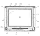
まず、本発明の第1実施形態における電気光学装置の画素部における構成について、図1から図4を参照して説明する。ここに図1は、電気光学装置の画像表示領域を構成するマトリクス状に形成された複数の画素における各種素子、配線等の等価回路である。図2は、データ線、走査線、画素電極等が形成されたTFTアレイ基板の相隣接する複数の画素群の平面図であり、図3は、図2のうち特にデータ線、シールド層及び画素電極の配置関係を示すためこれらの要素を抜き出して描いた平面図である。また、図4は、図2のA−A´断面図である。なお、図4においては、各層・各部材を図面上で認識可能な程度の大きさとするため、該各層・各部材ごとに縮尺を異ならしめてある。
このシールド層400は、画素電極9aが配置された画像表示領域10aからその周囲に延設され、定電位源と電気的に接続されることで、固定電位とされている。なお、ここに述べた「定電位源」としては、データ線駆動回路101に供給される正電源や負電源の定電位源でもよいし、対向基板20の対向電極21に供給される定電位源でも構わない。
次に、本発明の第2実施形態の電気光学装置について、図5から図8を参照しながら説明する。ここに図5は、図2と同趣旨の図であって、シールド層及びデータ線等の構成について異なる態様となるものを示すものであり、図6は、図4と同趣旨の図であって図5のA−A´断面図であり、データ線及びシールド層等の構成について異なる態様となるものを示すものである。また、図7は、データ線上に形成される窒化膜の態様を示す平面図であり、図8は、図5のB−B´断面図であり、図9は、図8の変形形態に係る図である。なお、第2実施形態の電気光学装置は、上記の第1実施形態の電気光学装置の画素部における構成と略同様な構成を備えている。したがって、以下では、第2実施形態において特徴的な部分のみについて主な説明を加えることとし、残余の部分については、その説明を適宜省略ないし簡略化することとする。
この蓄積容量70は、TFT30とデータ線6aとの間に形成されるので、図5に示すように、走査線3aの延設方向並びにデータ線6aの延設方向に十字形状に形成されている。これにより、蓄積容量を増大化でき、遮光性の容量電極300により、TFT30への遮光性を高めることができる。また、蓄積容量70は、下側遮光膜11やシールド層400が形成されている画素電極6aの角部に形成すると、より蓄積容量の増大化、遮光性を高めることができる。
また、この第2層間絶縁膜42には、前述のシールド層用中継層6a1及び第2中継層6a2に対応するように、コンタクトホール801及び前記のコンタクトホール882が開孔されている。
また、この第5層には、シールド層404と同一膜として、第3中継層406が形成されている。
以上のように構成された各実施形態における電気光学装置の全体構成を図16及び図17を参照して説明する。なお、図16は、TFTアレイ基板をその上に形成された各構成要素とともに対向基板20の側からみた平面図であり、図17は図16のH−H´断面図である。
また、対向基板20のコーナ部の少なくとも一箇所においては、TFTアレイ基板10と対向基板20との間で電気的に導通をとるための導通材106が設けられている。
次に、以上詳細に説明した電気光学装置をライトバルブとして用いた電子機器の一例たる投射型カラー表示装置の実施形態について、その全体構成、特に光学的な構成について説明する。ここに、図18は、投射型カラー表示装置の図式的断面図である。
1a´…チャネル領域
2…絶縁膜
3a…走査線
3b…水平的突出部(垂直的突出部を含む)
3c…包囲部(垂直的突出部を含む)
6a、6a1、6a2…データ線
9a…画素電極
10…TFTアレイ基板
10a…画像表示領域
16…配向膜
20…対向基板
21…対向電極
22…配向膜
30…TFT
43…第3層間絶縁膜
401、401´…窒化膜
Claims (20)
- 基板上に、第1方向に延在するデータ線及び該データ線に交差する第2方向に延在する走査線、並びに、前記データ線及び前記走査線の交差領域に対応するように配置された画素電極及び薄膜トランジスタが積層構造の一部をなして備えられた電気光学装置であって、
前記基板上には更に、
前記薄膜トランジスタ及び前記画素電極に電気的に接続された蓄積容量と、
前記データ線及び前記画素電極間に配置されたシールド層とが、前記積層構造の一部をなして備えられてなり、
前記シールド層には、窒化膜が含まれ、前記データ線に沿い、かつ、前記データ線よりも幅広に形成されていることを特徴とする電気光学装置。 - 前記画素電極の下地として配置された層間絶縁膜の表面は平坦化処理が施されていることを特徴とする請求項1記載の電気光学装置。
- 前記データ線は、前記蓄積容量を構成する一対の電極の一方と同一膜として形成されていることを特徴とする請求項1又は2に記載の電気光学装置。
- 前記データ線は、アルミニウム膜及び導電性のポリシリコン膜の積層体を構成していることを特徴とする請求項3に記載の電気光学装置。
- 前記蓄積容量を構成する一対の電極の一方と前記画素電極を電気的に接続する中継層が前記積層構造の一部として更に備えられていることを特徴とする請求項1乃至4のいずれか一項に記載の電気光学装置。
- 前記中継層は、アルミニウム膜及び窒化膜からなることを特徴とする請求項5に記載の電気光学装置。
- 前記シールド層は、前記中継層と同一膜として形成されていることを特徴とする請求項5又は6に記載の電気光学装置。
- 前記データ線の表面上には、窒化膜が備えられていることを特徴とする請求項1に記載の電気光学装置。
- 基板上に、第1方向に延在するデータ線及び該データ線に交差する第2方向に延在する走査線、並びに、前記データ線及び前記走査線の交差領域に対応するように配置された画素電極及び薄膜トランジスタが積層構造の一部をなして備えられた電気光学装置であって、
前記基板上には更に、
前記薄膜トランジスタ及び前記画素電極に電気的に接続された蓄積容量と、
前記データ線及び前記画素電極間に配置されたシールド層とが、前記積層構造の一部をなして備えられてなり、
前記データ線には、窒化膜が含まれていることを特徴とする電気光学装置。 - 前記窒化膜は、前記走査線が延在する領域に形成されていることを特徴とする請求項9に記載の電気光学装置。
- 前記窒化膜は、前記画素電極、前記データ線及び前記走査線が形成される領域として規定される画像表示領域の周囲に形成されていることを特徴とする請求項9又は10に記載の電気光学装置。
- 前記データ線上に形成される前記窒化膜の幅は、該データ線の幅よりも大きくされていることを特徴とする請求項9乃至10のいずれか一項に記載の電気光学装置。
- 前記窒化膜の縁は、前記データ線の縁よりも、その両側につきそれぞれ0.1〜2.2μmだけ大きくされていることを特徴とする請求項12に記載の電気光学装置。
- 前記窒化膜の厚さは、10〜100nmであることを特徴とする請求項9乃至13のいずれか一項に記載の電気光学装置。
- 前記基板に電気光学物質を挟んで対向する他の基板と、該他の基板上に前記走査線及び前記データ線と位置的に対応するように形成された遮光膜を更に備え、前記窒化膜の幅は、前記遮光膜の幅よりも小さくされていることを特徴とする請求項9乃至14のいずれか一項に記載の電気光学装置。
- 前記窒化膜の縁は、前記遮光膜の縁よりも、その両側につきそれぞれ1μm以内で小さく形成されていることを特徴とする請求項15に記載の電気光学装置。
- 前記基板に電気光学物質を挟んで対向する他の基板と、該他の基板上に前記走査線及び前記データ線と位置的に対応するように形成された遮光膜を更に備え、前記窒化膜の幅は、前記遮光膜の幅よりも大きくされていることを特徴とする請求項9乃至14のいずれか一項に記載の電気光学装置。
- 前記シールド層は、透明導電性材料からなるとともに、前記基板の全面に関してベタ状に形成されていることを特徴とする請求項1乃至17のいずれか一項に記載の電気光学装置。
- 基板上に、第1方向に延在するデータ線及び該データ線に交差する第2方向に延在する走査線、並びに、前記データ線及び前記走査線の交差領域に対応するように配置された画素電極及び薄膜トランジスタが積層構造の一部をなして備えられた電気光学装置であって、
前記基板上には更に、
前記薄膜トランジスタ及び前記画素電極に電気的に接続された蓄積容量と、
前記データ線及び前記画素電極間に配置された遮光膜とが、前記積層構造の一部をなして備えられてなり、
前記蓄積容量を構成する誘電体膜は、相異なる材料を含む複数の層からなるとともに、そのうちの一の層は他の層に比べて高誘電率材料からなる層を含む積層体を構成しており、
前記データ線には、窒化膜が含まれていることを特徴とする電気光学装置。 - 請求項1乃至19のいずれか一項に記載の電気光学装置を具備してなることを特徴とする電子機器。
Priority Applications (6)
| Application Number | Priority Date | Filing Date | Title |
|---|---|---|---|
| JP2003321789A JP3791517B2 (ja) | 2002-10-31 | 2003-09-12 | 電気光学装置及び電子機器 |
| US10/690,270 US7193663B2 (en) | 2002-10-31 | 2003-10-22 | Electro-optical device and electronic apparatus |
| KR1020030076263A KR100564509B1 (ko) | 2002-10-31 | 2003-10-30 | 전기 광학 장치 및 전자 기기 |
| CN2003101030862A CN1499274B (zh) | 2002-10-31 | 2003-10-30 | 电光装置和电子设备 |
| TW092130283A TWI237219B (en) | 2002-10-31 | 2003-10-30 | Opto-electronic device and electronic machine |
| US11/598,731 US7317497B2 (en) | 2002-10-31 | 2006-11-14 | Electro-optical device and electronic apparatus |
Applications Claiming Priority (2)
| Application Number | Priority Date | Filing Date | Title |
|---|---|---|---|
| JP2002318544 | 2002-10-31 | ||
| JP2003321789A JP3791517B2 (ja) | 2002-10-31 | 2003-09-12 | 電気光学装置及び電子機器 |
Related Child Applications (1)
| Application Number | Title | Priority Date | Filing Date |
|---|---|---|---|
| JP2005318082A Division JP2006065356A (ja) | 2002-10-31 | 2005-11-01 | 電気光学装置及び電子機器 |
Publications (2)
| Publication Number | Publication Date |
|---|---|
| JP2004170917A true JP2004170917A (ja) | 2004-06-17 |
| JP3791517B2 JP3791517B2 (ja) | 2006-06-28 |
Family
ID=32715877
Family Applications (1)
| Application Number | Title | Priority Date | Filing Date |
|---|---|---|---|
| JP2003321789A Expired - Lifetime JP3791517B2 (ja) | 2002-10-31 | 2003-09-12 | 電気光学装置及び電子機器 |
Country Status (5)
| Country | Link |
|---|---|
| US (2) | US7193663B2 (ja) |
| JP (1) | JP3791517B2 (ja) |
| KR (1) | KR100564509B1 (ja) |
| CN (1) | CN1499274B (ja) |
| TW (1) | TWI237219B (ja) |
Cited By (1)
| Publication number | Priority date | Publication date | Assignee | Title |
|---|---|---|---|---|
| JP2007140458A (ja) * | 2005-11-23 | 2007-06-07 | Samsung Sdi Co Ltd | 液晶表示装置アレイ基板及びその製造方法 |
Families Citing this family (20)
| Publication number | Priority date | Publication date | Assignee | Title |
|---|---|---|---|---|
| JP4319517B2 (ja) * | 2003-10-28 | 2009-08-26 | 東芝モバイルディスプレイ株式会社 | アレイ基板および平面表示装置 |
| KR100587370B1 (ko) * | 2003-10-29 | 2006-06-08 | 엘지.필립스 엘시디 주식회사 | 액정 표시 장치 |
| CN101044627B (zh) | 2004-09-15 | 2012-02-08 | 株式会社半导体能源研究所 | 半导体器件 |
| JP2006243579A (ja) * | 2005-03-07 | 2006-09-14 | Seiko Epson Corp | 電気光学装置及びその製造方法、並びに電子機器 |
| US7851989B2 (en) | 2005-03-25 | 2010-12-14 | Semiconductor Energy Laboratory Co., Ltd. | Light emitting device |
| JP4349375B2 (ja) * | 2005-04-11 | 2009-10-21 | セイコーエプソン株式会社 | 電気光学装置及び電子機器 |
| JP4442569B2 (ja) * | 2005-04-11 | 2010-03-31 | セイコーエプソン株式会社 | 電気光学装置及び電子機器 |
| JP4241777B2 (ja) * | 2006-07-25 | 2009-03-18 | セイコーエプソン株式会社 | 電気光学装置及び電子機器 |
| TWM325514U (en) * | 2007-06-26 | 2008-01-11 | Wintek Corp | Active matrix substrate and liquid crystal display thereof |
| US8144281B2 (en) * | 2007-08-09 | 2012-03-27 | Seiko Epson Corporation | Electro-optical device having a light shielding film with first, second, and third portions |
| JP5648437B2 (ja) * | 2010-11-15 | 2015-01-07 | セイコーエプソン株式会社 | 電気光学装置および投射型表示装置 |
| JP5810589B2 (ja) * | 2011-04-01 | 2015-11-11 | セイコーエプソン株式会社 | 電気光学装置、投射型表示装置、および電子機器 |
| GB2489939A (en) * | 2011-04-11 | 2012-10-17 | Plastic Logic Ltd | Control of capacitive coupling in pixel circuitry |
| TW201340181A (zh) * | 2012-03-30 | 2013-10-01 | Chunghwa Picture Tubes Ltd | 觸控面板及其觸碰感應層的製造方法 |
| KR102090713B1 (ko) | 2013-06-25 | 2020-03-19 | 삼성디스플레이 주식회사 | 가요성 표시 패널 및 상기 가요성 표시 패널의 제조 방법 |
| US9964820B2 (en) * | 2014-02-04 | 2018-05-08 | Apple Inc. | Displays with flipped panel structures |
| JP2016134388A (ja) | 2015-01-15 | 2016-07-25 | 株式会社ジャパンディスプレイ | 表示装置 |
| KR102638298B1 (ko) * | 2016-05-16 | 2024-02-20 | 삼성디스플레이 주식회사 | 디스플레이 장치 |
| JP2019518249A (ja) * | 2016-05-31 | 2019-06-27 | イー インク コーポレイション | 電気光学ディスプレイのためのバックプレーン |
| JP6813045B2 (ja) * | 2019-03-14 | 2021-01-13 | セイコーエプソン株式会社 | 電気光学装置および電子機器 |
Family Cites Families (50)
| Publication number | Priority date | Publication date | Assignee | Title |
|---|---|---|---|---|
| JPS5846644A (ja) | 1981-09-14 | 1983-03-18 | Oki Electric Ind Co Ltd | 半導体素子 |
| JPH02251172A (ja) | 1989-03-24 | 1990-10-08 | Hitachi Ltd | 半導体集積回路装置及びその製造方法 |
| JP2502789B2 (ja) | 1990-05-17 | 1996-05-29 | 松下電器産業株式会社 | 薄膜トランジスタの製造方法 |
| JP3583153B2 (ja) | 1991-09-13 | 2004-10-27 | 株式会社ルネサステクノロジ | 半導体装置及びその製造方法 |
| SG81187A1 (en) * | 1991-11-29 | 2001-06-19 | Seiko Epson Corp | Liquid crystal display device and manufacturing method therefor |
| JP3082396B2 (ja) | 1992-01-29 | 2000-08-28 | 日本電気株式会社 | 半導体装置の製造方法 |
| JP2950061B2 (ja) | 1992-11-13 | 1999-09-20 | 日本電気株式会社 | 液晶表示素子 |
| KR100268007B1 (ko) * | 1992-12-22 | 2000-10-16 | 구본준 | 액정표시소자 제조방법 |
| JP3109967B2 (ja) * | 1993-12-28 | 2000-11-20 | キヤノン株式会社 | アクティブマトリクス基板の製造方法 |
| JP3308100B2 (ja) | 1994-04-28 | 2002-07-29 | ローム株式会社 | Tft型液晶表示装置 |
| US5546204A (en) * | 1994-05-26 | 1996-08-13 | Honeywell Inc. | TFT matrix liquid crystal device having data source lines and drain means of etched and doped single crystal silicon |
| US5563727A (en) * | 1994-06-30 | 1996-10-08 | Honeywell Inc. | High aperture AMLCD with nonparallel alignment of addressing lines to the pixel edges or with distributed analog processing at the pixel level |
| JPH08306902A (ja) | 1995-04-28 | 1996-11-22 | Olympus Optical Co Ltd | 固体撮像装置 |
| JP3650405B2 (ja) * | 1995-09-14 | 2005-05-18 | 株式会社 日立製作所 | アクティブマトリクス型液晶表示装置 |
| US5978056A (en) * | 1995-10-15 | 1999-11-02 | Victor Company Of Japan, Ltd | Reflection-type display apparatus having antireflection films |
| JPH09232426A (ja) | 1996-02-23 | 1997-09-05 | Toshiba Corp | 多層配線構造を有する半導体装置の製造方法 |
| JP3708637B2 (ja) * | 1996-07-15 | 2005-10-19 | 株式会社半導体エネルギー研究所 | 液晶表示装置 |
| JPH1039336A (ja) | 1996-07-26 | 1998-02-13 | Toshiba Corp | アクティブマトリクス型液晶表示装置 |
| JP4307574B2 (ja) * | 1996-09-03 | 2009-08-05 | 株式会社半導体エネルギー研究所 | アクティブマトリクス表示装置 |
| JP3541650B2 (ja) | 1996-10-22 | 2004-07-14 | セイコーエプソン株式会社 | 液晶パネル用基板、液晶パネル、及びそれを用いた電子機器並びに投写型表示装置 |
| JPH10242268A (ja) | 1997-02-27 | 1998-09-11 | Sony Corp | 多層配線構造における接続孔の埋め込み方法 |
| JPH10307305A (ja) | 1997-03-07 | 1998-11-17 | Toshiba Corp | アレイ基板、液晶表示装置及びそれらの製造方法 |
| JP3097839B2 (ja) | 1997-09-04 | 2000-10-10 | 日本電気株式会社 | 半導体装置およびその製造方法 |
| FR2769924B1 (fr) * | 1997-10-20 | 2000-03-10 | Centre Nat Rech Scient | Procede de realisation d'une couche epitaxiale de nitrure de gallium, couche epitaxiale de nitrure de gallium et composant optoelectronique muni d'une telle couche |
| JP3288615B2 (ja) * | 1997-10-21 | 2002-06-04 | 株式会社アドバンスト・ディスプレイ | 薄膜トランジスタの製造方法 |
| JP2918875B1 (ja) | 1998-03-02 | 1999-07-12 | インターナショナル・ビジネス・マシーンズ・コーポレイション | 反射型液晶素子、製造方法およびプロジェクション表示装置 |
| JP3736122B2 (ja) | 1998-06-23 | 2006-01-18 | セイコーエプソン株式会社 | 液晶装置及び電子機器 |
| US5940718A (en) * | 1998-07-20 | 1999-08-17 | Advanced Micro Devices | Nitridation assisted polysilicon sidewall protection in self-aligned shallow trench isolation |
| JP2000094072A (ja) | 1998-09-22 | 2000-04-04 | Amada Co Ltd | 板材加工機のワーク搬入・搬出方法およびその装置 |
| CN1153180C (zh) | 1998-11-26 | 2004-06-09 | 精工爱普生株式会社 | 电光装置及其制造方法和电子装置 |
| JP4403329B2 (ja) | 1999-08-30 | 2010-01-27 | ソニー株式会社 | 液晶表示装置の製造方法 |
| JP3488681B2 (ja) * | 1999-10-26 | 2004-01-19 | シャープ株式会社 | 液晶表示装置 |
| JP2001133810A (ja) | 1999-11-08 | 2001-05-18 | Sony Corp | 液晶表示装置及びその製造方法 |
| JP3524029B2 (ja) * | 2000-01-04 | 2004-04-26 | インターナショナル・ビジネス・マシーンズ・コーポレーション | トップゲート型tft構造を形成する方法 |
| CN1227751C (zh) * | 2000-02-17 | 2005-11-16 | Lg电子株式会社 | 有机电致发光显示板及其封装方法 |
| TWI301915B (ja) * | 2000-03-17 | 2008-10-11 | Seiko Epson Corp | |
| JP3799943B2 (ja) | 2000-03-17 | 2006-07-19 | セイコーエプソン株式会社 | 電気光学装置およびプロジェクタ |
| TWI222047B (en) | 2000-04-21 | 2004-10-11 | Seiko Epson Corp | Electro-optical device |
| WO2001081994A1 (en) | 2000-04-21 | 2001-11-01 | Seiko Epson Corporation | Electrooptic device, projection type display and method for manufacturing electrooptic device |
| KR100695299B1 (ko) * | 2000-05-12 | 2007-03-14 | 삼성전자주식회사 | 액정 표시 장치용 박막 트랜지스터 기판 및 그의 제조 방법 |
| JP3731447B2 (ja) | 2000-06-15 | 2006-01-05 | セイコーエプソン株式会社 | 電気光学装置及びその製造方法 |
| JP3460706B2 (ja) * | 2000-08-07 | 2003-10-27 | セイコーエプソン株式会社 | 電気光学装置、電子機器、電気光学装置用基板および電気光学装置用基板の製造方法。 |
| JP2002122857A (ja) | 2000-08-07 | 2002-04-26 | Seiko Epson Corp | 電気光学装置、電子機器、電気光学装置用基板および電気光学装置用基板の製造方法、並びに遮光膜 |
| JP3918412B2 (ja) | 2000-08-10 | 2007-05-23 | ソニー株式会社 | 薄膜半導体装置及び液晶表示装置とこれらの製造方法 |
| US6636284B2 (en) * | 2000-08-11 | 2003-10-21 | Seiko Epson Corporation | System and method for providing an electro-optical device having light shield layers |
| JP4075299B2 (ja) | 2000-09-20 | 2008-04-16 | セイコーエプソン株式会社 | 電気光学装置用素子基板及びそれを用いた電気光学装置 |
| JP2002131778A (ja) | 2000-10-23 | 2002-05-09 | Seiko Epson Corp | 電気光学装置用基板およびこれを備えた電気光学装置並びに電子機器 |
| JP3873610B2 (ja) | 2000-11-17 | 2007-01-24 | セイコーエプソン株式会社 | 電気光学装置及びその製造方法並びにプロジェクタ |
| JP3937721B2 (ja) | 2000-11-21 | 2007-06-27 | セイコーエプソン株式会社 | 電気光学装置及びその製造方法並びにプロジェクタ |
| JP3821067B2 (ja) * | 2002-07-11 | 2006-09-13 | セイコーエプソン株式会社 | 電気光学装置及び電子機器 |
-
2003
- 2003-09-12 JP JP2003321789A patent/JP3791517B2/ja not_active Expired - Lifetime
- 2003-10-22 US US10/690,270 patent/US7193663B2/en not_active Expired - Lifetime
- 2003-10-30 TW TW092130283A patent/TWI237219B/zh not_active IP Right Cessation
- 2003-10-30 KR KR1020030076263A patent/KR100564509B1/ko not_active Expired - Fee Related
- 2003-10-30 CN CN2003101030862A patent/CN1499274B/zh not_active Expired - Lifetime
-
2006
- 2006-11-14 US US11/598,731 patent/US7317497B2/en not_active Expired - Lifetime
Cited By (1)
| Publication number | Priority date | Publication date | Assignee | Title |
|---|---|---|---|---|
| JP2007140458A (ja) * | 2005-11-23 | 2007-06-07 | Samsung Sdi Co Ltd | 液晶表示装置アレイ基板及びその製造方法 |
Also Published As
| Publication number | Publication date |
|---|---|
| TW200416640A (en) | 2004-09-01 |
| US20050088596A1 (en) | 2005-04-28 |
| CN1499274B (zh) | 2010-06-23 |
| CN1499274A (zh) | 2004-05-26 |
| US20070058102A1 (en) | 2007-03-15 |
| KR100564509B1 (ko) | 2006-03-29 |
| TWI237219B (en) | 2005-08-01 |
| US7193663B2 (en) | 2007-03-20 |
| US7317497B2 (en) | 2008-01-08 |
| JP3791517B2 (ja) | 2006-06-28 |
| KR20040038829A (ko) | 2004-05-08 |
Similar Documents
| Publication | Publication Date | Title |
|---|---|---|
| JP3870941B2 (ja) | 電気光学装置及び電子機器 | |
| JP3858880B2 (ja) | 電気光学装置及び電子機器 | |
| JP4045226B2 (ja) | 電気光学装置及び電子機器 | |
| JP3791517B2 (ja) | 電気光学装置及び電子機器 | |
| JP3767590B2 (ja) | 電気光学装置及びその製造方法並びに電子機器 | |
| JP4095518B2 (ja) | 電気光学装置及び電子機器 | |
| CN1325967C (zh) | 电光装置及电子设备 | |
| JP2004170915A (ja) | 電気光学装置及び電子機器 | |
| JP4186767B2 (ja) | 電気光学装置及び電子機器 | |
| JP2004102058A (ja) | 電気光学装置及び電子機器 | |
| JP4506133B2 (ja) | 電気光学装置及び電子機器 | |
| JP3835403B2 (ja) | 電気光学装置及び電子機器 | |
| JP2004170910A (ja) | 電気光学装置及び電子機器 | |
| JP4214741B2 (ja) | 電気光学装置及び電子機器 | |
| JP4862936B2 (ja) | 電気光学装置及び電子機器 | |
| JP4003724B2 (ja) | 電気光学装置及び電子機器 | |
| CN100480826C (zh) | 电光装置及电子设备 | |
| JP4730407B2 (ja) | 電気光学装置及び電子機器 | |
| JP3925549B2 (ja) | 電気光学装置及び電子機器 | |
| JP2004170912A (ja) | 電気光学装置及び電子機器 | |
| JP2004170918A (ja) | 電気光学装置及び電子機器 | |
| JP2004170914A (ja) | 電気光学装置及び電子機器 | |
| JP2004191930A (ja) | 電気光学装置及びその製造方法並びに電子機器 | |
| JP2006065356A (ja) | 電気光学装置及び電子機器 | |
| JP2004170920A (ja) | 電気光学装置及び電子機器 |
Legal Events
| Date | Code | Title | Description |
|---|---|---|---|
| A977 | Report on retrieval |
Free format text: JAPANESE INTERMEDIATE CODE: A971007 Effective date: 20050218 |
|
| A131 | Notification of reasons for refusal |
Free format text: JAPANESE INTERMEDIATE CODE: A131 Effective date: 20050705 |
|
| A521 | Request for written amendment filed |
Free format text: JAPANESE INTERMEDIATE CODE: A523 Effective date: 20050727 |
|
| A02 | Decision of refusal |
Free format text: JAPANESE INTERMEDIATE CODE: A02 Effective date: 20051018 |
|
| A521 | Request for written amendment filed |
Free format text: JAPANESE INTERMEDIATE CODE: A523 Effective date: 20051101 |
|
| A911 | Transfer to examiner for re-examination before appeal (zenchi) |
Free format text: JAPANESE INTERMEDIATE CODE: A911 Effective date: 20051208 |
|
| A131 | Notification of reasons for refusal |
Free format text: JAPANESE INTERMEDIATE CODE: A131 Effective date: 20060117 |
|
| A521 | Request for written amendment filed |
Free format text: JAPANESE INTERMEDIATE CODE: A523 Effective date: 20060130 |
|
| TRDD | Decision of grant or rejection written | ||
| A01 | Written decision to grant a patent or to grant a registration (utility model) |
Free format text: JAPANESE INTERMEDIATE CODE: A01 Effective date: 20060314 |
|
| A61 | First payment of annual fees (during grant procedure) |
Free format text: JAPANESE INTERMEDIATE CODE: A61 Effective date: 20060327 |
|
| R150 | Certificate of patent or registration of utility model |
Free format text: JAPANESE INTERMEDIATE CODE: R150 Ref document number: 3791517 Country of ref document: JP Free format text: JAPANESE INTERMEDIATE CODE: R150 |
|
| FPAY | Renewal fee payment (event date is renewal date of database) |
Free format text: PAYMENT UNTIL: 20090414 Year of fee payment: 3 |
|
| FPAY | Renewal fee payment (event date is renewal date of database) |
Free format text: PAYMENT UNTIL: 20100414 Year of fee payment: 4 |
|
| FPAY | Renewal fee payment (event date is renewal date of database) |
Free format text: PAYMENT UNTIL: 20110414 Year of fee payment: 5 |
|
| FPAY | Renewal fee payment (event date is renewal date of database) |
Free format text: PAYMENT UNTIL: 20110414 Year of fee payment: 5 |
|
| FPAY | Renewal fee payment (event date is renewal date of database) |
Free format text: PAYMENT UNTIL: 20120414 Year of fee payment: 6 |
|
| FPAY | Renewal fee payment (event date is renewal date of database) |
Free format text: PAYMENT UNTIL: 20130414 Year of fee payment: 7 |
|
| FPAY | Renewal fee payment (event date is renewal date of database) |
Free format text: PAYMENT UNTIL: 20130414 Year of fee payment: 7 |
|
| FPAY | Renewal fee payment (event date is renewal date of database) |
Free format text: PAYMENT UNTIL: 20140414 Year of fee payment: 8 |
|
| S531 | Written request for registration of change of domicile |
Free format text: JAPANESE INTERMEDIATE CODE: R313531 |
|
| R350 | Written notification of registration of transfer |
Free format text: JAPANESE INTERMEDIATE CODE: R350 |
|
| R250 | Receipt of annual fees |
Free format text: JAPANESE INTERMEDIATE CODE: R250 |
|
| R250 | Receipt of annual fees |
Free format text: JAPANESE INTERMEDIATE CODE: R250 |
|
| R250 | Receipt of annual fees |
Free format text: JAPANESE INTERMEDIATE CODE: R250 |
|
| R250 | Receipt of annual fees |
Free format text: JAPANESE INTERMEDIATE CODE: R250 |
|
| S111 | Request for change of ownership or part of ownership |
Free format text: JAPANESE INTERMEDIATE CODE: R313113 |
|
| R360 | Written notification for declining of transfer of rights |
Free format text: JAPANESE INTERMEDIATE CODE: R360 |
|
| R360 | Written notification for declining of transfer of rights |
Free format text: JAPANESE INTERMEDIATE CODE: R360 |
|
| R371 | Transfer withdrawn |
Free format text: JAPANESE INTERMEDIATE CODE: R371 |
|
| S111 | Request for change of ownership or part of ownership |
Free format text: JAPANESE INTERMEDIATE CODE: R313113 |
|
| R350 | Written notification of registration of transfer |
Free format text: JAPANESE INTERMEDIATE CODE: R350 |
|
| R250 | Receipt of annual fees |
Free format text: JAPANESE INTERMEDIATE CODE: R250 |
|
| EXPY | Cancellation because of completion of term |