JP2004170917A - Electro-optical devices and electronic equipment - Google Patents
Electro-optical devices and electronic equipment Download PDFInfo
- Publication number
- JP2004170917A JP2004170917A JP2003321789A JP2003321789A JP2004170917A JP 2004170917 A JP2004170917 A JP 2004170917A JP 2003321789 A JP2003321789 A JP 2003321789A JP 2003321789 A JP2003321789 A JP 2003321789A JP 2004170917 A JP2004170917 A JP 2004170917A
- Authority
- JP
- Japan
- Prior art keywords
- data line
- electro
- film
- optical device
- layer
- Prior art date
- Legal status (The legal status is an assumption and is not a legal conclusion. Google has not performed a legal analysis and makes no representation as to the accuracy of the status listed.)
- Granted
Links
- 239000010410 layer Substances 0.000 claims abstract description 355
- 150000004767 nitrides Chemical class 0.000 claims abstract description 133
- 239000000758 substrate Substances 0.000 claims abstract description 112
- 239000003990 capacitor Substances 0.000 claims abstract description 101
- 238000003860 storage Methods 0.000 claims abstract description 58
- 239000011229 interlayer Substances 0.000 claims abstract description 52
- 239000010408 film Substances 0.000 claims description 424
- 239000000463 material Substances 0.000 claims description 32
- 239000010409 thin film Substances 0.000 claims description 29
- 229910052782 aluminium Inorganic materials 0.000 claims description 26
- XAGFODPZIPBFFR-UHFFFAOYSA-N aluminium Chemical compound [Al] XAGFODPZIPBFFR-UHFFFAOYSA-N 0.000 claims description 26
- 238000000034 method Methods 0.000 claims description 25
- 229910021420 polycrystalline silicon Inorganic materials 0.000 claims description 21
- 229920005591 polysilicon Polymers 0.000 claims description 21
- 230000008569 process Effects 0.000 claims description 16
- 239000004020 conductor Substances 0.000 claims description 10
- 239000007787 solid Substances 0.000 claims description 9
- 230000000694 effects Effects 0.000 abstract description 34
- 230000008878 coupling Effects 0.000 abstract description 23
- 238000010168 coupling process Methods 0.000 abstract description 23
- 238000005859 coupling reaction Methods 0.000 abstract description 23
- 238000010586 diagram Methods 0.000 abstract description 6
- 239000004065 semiconductor Substances 0.000 description 35
- 239000004973 liquid crystal related substance Substances 0.000 description 31
- 230000006870 function Effects 0.000 description 20
- 229910052814 silicon oxide Inorganic materials 0.000 description 19
- 229910052581 Si3N4 Inorganic materials 0.000 description 17
- VYPSYNLAJGMNEJ-UHFFFAOYSA-N Silicium dioxide Chemical compound O=[Si]=O VYPSYNLAJGMNEJ-UHFFFAOYSA-N 0.000 description 17
- 238000004519 manufacturing process Methods 0.000 description 17
- HQVNEWCFYHHQES-UHFFFAOYSA-N silicon nitride Chemical compound N12[Si]34N5[Si]62N3[Si]51N64 HQVNEWCFYHHQES-UHFFFAOYSA-N 0.000 description 17
- 238000000059 patterning Methods 0.000 description 15
- 238000005530 etching Methods 0.000 description 14
- NRTOMJZYCJJWKI-UHFFFAOYSA-N Titanium nitride Chemical compound [Ti]#N NRTOMJZYCJJWKI-UHFFFAOYSA-N 0.000 description 13
- 238000002834 transmittance Methods 0.000 description 13
- 229910052751 metal Inorganic materials 0.000 description 11
- 239000002184 metal Substances 0.000 description 11
- 230000003405 preventing effect Effects 0.000 description 11
- 239000011159 matrix material Substances 0.000 description 10
- 239000005368 silicate glass Substances 0.000 description 9
- 230000007797 corrosion Effects 0.000 description 8
- 238000005260 corrosion Methods 0.000 description 8
- 230000035515 penetration Effects 0.000 description 7
- 229910045601 alloy Inorganic materials 0.000 description 6
- 239000000956 alloy Substances 0.000 description 6
- 230000015572 biosynthetic process Effects 0.000 description 6
- 239000005380 borophosphosilicate glass Substances 0.000 description 6
- 230000008859 change Effects 0.000 description 6
- 230000005684 electric field Effects 0.000 description 6
- 239000003566 sealing material Substances 0.000 description 6
- 230000006378 damage Effects 0.000 description 5
- 230000007547 defect Effects 0.000 description 5
- 238000009792 diffusion process Methods 0.000 description 5
- 239000011347 resin Substances 0.000 description 5
- 229920005989 resin Polymers 0.000 description 5
- XLYOFNOQVPJJNP-UHFFFAOYSA-N water Substances O XLYOFNOQVPJJNP-UHFFFAOYSA-N 0.000 description 5
- XUIMIQQOPSSXEZ-UHFFFAOYSA-N Silicon Chemical compound [Si] XUIMIQQOPSSXEZ-UHFFFAOYSA-N 0.000 description 4
- 230000005540 biological transmission Effects 0.000 description 4
- 239000011651 chromium Substances 0.000 description 4
- 239000013078 crystal Substances 0.000 description 4
- 230000007423 decrease Effects 0.000 description 4
- 239000011521 glass Substances 0.000 description 4
- 230000008595 infiltration Effects 0.000 description 4
- 238000001764 infiltration Methods 0.000 description 4
- 238000009413 insulation Methods 0.000 description 4
- 239000002243 precursor Substances 0.000 description 4
- 229910052710 silicon Inorganic materials 0.000 description 4
- 239000010703 silicon Substances 0.000 description 4
- 239000010936 titanium Substances 0.000 description 4
- 230000000903 blocking effect Effects 0.000 description 3
- 229910052804 chromium Inorganic materials 0.000 description 3
- 230000004048 modification Effects 0.000 description 3
- 238000012986 modification Methods 0.000 description 3
- 229910052750 molybdenum Inorganic materials 0.000 description 3
- 238000000206 photolithography Methods 0.000 description 3
- 238000005498 polishing Methods 0.000 description 3
- 239000003870 refractory metal Substances 0.000 description 3
- 229910021332 silicide Inorganic materials 0.000 description 3
- FVBUAEGBCNSCDD-UHFFFAOYSA-N silicide(4-) Chemical compound [Si-4] FVBUAEGBCNSCDD-UHFFFAOYSA-N 0.000 description 3
- 229910052715 tantalum Inorganic materials 0.000 description 3
- 229910052719 titanium Inorganic materials 0.000 description 3
- 229910052721 tungsten Inorganic materials 0.000 description 3
- 239000004988 Nematic liquid crystal Substances 0.000 description 2
- 229910003070 TaOx Inorganic materials 0.000 description 2
- 229910010413 TiO 2 Inorganic materials 0.000 description 2
- ATJFFYVFTNAWJD-UHFFFAOYSA-N Tin Chemical compound [Sn] ATJFFYVFTNAWJD-UHFFFAOYSA-N 0.000 description 2
- RTAQQCXQSZGOHL-UHFFFAOYSA-N Titanium Chemical compound [Ti] RTAQQCXQSZGOHL-UHFFFAOYSA-N 0.000 description 2
- 230000009471 action Effects 0.000 description 2
- PNEYBMLMFCGWSK-UHFFFAOYSA-N aluminium oxide Inorganic materials [O-2].[O-2].[O-2].[Al+3].[Al+3] PNEYBMLMFCGWSK-UHFFFAOYSA-N 0.000 description 2
- 230000004888 barrier function Effects 0.000 description 2
- 239000011324 bead Substances 0.000 description 2
- 238000006243 chemical reaction Methods 0.000 description 2
- 239000003086 colorant Substances 0.000 description 2
- 238000010292 electrical insulation Methods 0.000 description 2
- 238000005401 electroluminescence Methods 0.000 description 2
- 230000003628 erosive effect Effects 0.000 description 2
- 239000003365 glass fiber Substances 0.000 description 2
- 230000006872 improvement Effects 0.000 description 2
- 239000012535 impurity Substances 0.000 description 2
- AMGQUBHHOARCQH-UHFFFAOYSA-N indium;oxotin Chemical compound [In].[Sn]=O AMGQUBHHOARCQH-UHFFFAOYSA-N 0.000 description 2
- 238000010030 laminating Methods 0.000 description 2
- 230000031700 light absorption Effects 0.000 description 2
- 230000003287 optical effect Effects 0.000 description 2
- 230000002093 peripheral effect Effects 0.000 description 2
- 239000010453 quartz Substances 0.000 description 2
- 230000009467 reduction Effects 0.000 description 2
- 125000006850 spacer group Chemical group 0.000 description 2
- 239000000126 substance Substances 0.000 description 2
- 229920001187 thermosetting polymer Polymers 0.000 description 2
- 229910000838 Al alloy Inorganic materials 0.000 description 1
- ZOXJGFHDIHLPTG-UHFFFAOYSA-N Boron Chemical compound [B] ZOXJGFHDIHLPTG-UHFFFAOYSA-N 0.000 description 1
- VYZAMTAEIAYCRO-UHFFFAOYSA-N Chromium Chemical compound [Cr] VYZAMTAEIAYCRO-UHFFFAOYSA-N 0.000 description 1
- UFHFLCQGNIYNRP-UHFFFAOYSA-N Hydrogen Chemical compound [H][H] UFHFLCQGNIYNRP-UHFFFAOYSA-N 0.000 description 1
- ZOKXTWBITQBERF-UHFFFAOYSA-N Molybdenum Chemical compound [Mo] ZOKXTWBITQBERF-UHFFFAOYSA-N 0.000 description 1
- OAICVXFJPJFONN-UHFFFAOYSA-N Phosphorus Chemical compound [P] OAICVXFJPJFONN-UHFFFAOYSA-N 0.000 description 1
- 229910004298 SiO 2 Inorganic materials 0.000 description 1
- GWEVSGVZZGPLCZ-UHFFFAOYSA-N Titan oxide Chemical compound O=[Ti]=O GWEVSGVZZGPLCZ-UHFFFAOYSA-N 0.000 description 1
- GDFCWFBWQUEQIJ-UHFFFAOYSA-N [B].[P] Chemical compound [B].[P] GDFCWFBWQUEQIJ-UHFFFAOYSA-N 0.000 description 1
- WOIHABYNKOEWFG-UHFFFAOYSA-N [Sr].[Ba] Chemical compound [Sr].[Ba] WOIHABYNKOEWFG-UHFFFAOYSA-N 0.000 description 1
- 239000000853 adhesive Substances 0.000 description 1
- 230000001070 adhesive effect Effects 0.000 description 1
- 230000002411 adverse Effects 0.000 description 1
- 229910002113 barium titanate Inorganic materials 0.000 description 1
- 230000008901 benefit Effects 0.000 description 1
- 229910052796 boron Inorganic materials 0.000 description 1
- 230000015556 catabolic process Effects 0.000 description 1
- 238000004140 cleaning Methods 0.000 description 1
- 239000011248 coating agent Substances 0.000 description 1
- 238000000576 coating method Methods 0.000 description 1
- 230000000295 complement effect Effects 0.000 description 1
- 238000012790 confirmation Methods 0.000 description 1
- 238000013016 damping Methods 0.000 description 1
- 230000002950 deficient Effects 0.000 description 1
- 230000006866 deterioration Effects 0.000 description 1
- 230000002542 deteriorative effect Effects 0.000 description 1
- 238000001312 dry etching Methods 0.000 description 1
- 230000009977 dual effect Effects 0.000 description 1
- 238000001962 electrophoresis Methods 0.000 description 1
- 230000001747 exhibiting effect Effects 0.000 description 1
- 238000010304 firing Methods 0.000 description 1
- 229910000449 hafnium oxide Inorganic materials 0.000 description 1
- WIHZLLGSGQNAGK-UHFFFAOYSA-N hafnium(4+);oxygen(2-) Chemical compound [O-2].[O-2].[Hf+4] WIHZLLGSGQNAGK-UHFFFAOYSA-N 0.000 description 1
- 238000010438 heat treatment Methods 0.000 description 1
- 229910052739 hydrogen Inorganic materials 0.000 description 1
- 239000001257 hydrogen Substances 0.000 description 1
- 238000005984 hydrogenation reaction Methods 0.000 description 1
- 238000007689 inspection Methods 0.000 description 1
- 150000002500 ions Chemical class 0.000 description 1
- 230000007774 longterm Effects 0.000 description 1
- 229910001507 metal halide Inorganic materials 0.000 description 1
- 150000005309 metal halides Chemical class 0.000 description 1
- 238000002156 mixing Methods 0.000 description 1
- 239000011733 molybdenum Substances 0.000 description 1
- BPUBBGLMJRNUCC-UHFFFAOYSA-N oxygen(2-);tantalum(5+) Chemical compound [O-2].[O-2].[O-2].[O-2].[O-2].[Ta+5].[Ta+5] BPUBBGLMJRNUCC-UHFFFAOYSA-N 0.000 description 1
- RVTZCBVAJQQJTK-UHFFFAOYSA-N oxygen(2-);zirconium(4+) Chemical compound [O-2].[O-2].[Zr+4] RVTZCBVAJQQJTK-UHFFFAOYSA-N 0.000 description 1
- 230000000149 penetrating effect Effects 0.000 description 1
- 229910052698 phosphorus Inorganic materials 0.000 description 1
- 239000011574 phosphorus Substances 0.000 description 1
- 238000000016 photochemical curing Methods 0.000 description 1
- 238000005268 plasma chemical vapour deposition Methods 0.000 description 1
- 229920001721 polyimide Polymers 0.000 description 1
- 230000002265 prevention Effects 0.000 description 1
- 230000002035 prolonged effect Effects 0.000 description 1
- 238000005070 sampling Methods 0.000 description 1
- 238000007789 sealing Methods 0.000 description 1
- 239000002356 single layer Substances 0.000 description 1
- GUVRBAGPIYLISA-UHFFFAOYSA-N tantalum atom Chemical compound [Ta] GUVRBAGPIYLISA-UHFFFAOYSA-N 0.000 description 1
- 229910001936 tantalum oxide Inorganic materials 0.000 description 1
- OGIDPMRJRNCKJF-UHFFFAOYSA-N titanium oxide Inorganic materials [Ti]=O OGIDPMRJRNCKJF-UHFFFAOYSA-N 0.000 description 1
- WFKWXMTUELFFGS-UHFFFAOYSA-N tungsten Chemical compound [W] WFKWXMTUELFFGS-UHFFFAOYSA-N 0.000 description 1
- 239000010937 tungsten Substances 0.000 description 1
- YVTHLONGBIQYBO-UHFFFAOYSA-N zinc indium(3+) oxygen(2-) Chemical compound [O--].[Zn++].[In+3] YVTHLONGBIQYBO-UHFFFAOYSA-N 0.000 description 1
- 229910001928 zirconium oxide Inorganic materials 0.000 description 1
Images


Classifications
-
- G—PHYSICS
- G02—OPTICS
- G02F—OPTICAL DEVICES OR ARRANGEMENTS FOR THE CONTROL OF LIGHT BY MODIFICATION OF THE OPTICAL PROPERTIES OF THE MEDIA OF THE ELEMENTS INVOLVED THEREIN; NON-LINEAR OPTICS; FREQUENCY-CHANGING OF LIGHT; OPTICAL LOGIC ELEMENTS; OPTICAL ANALOGUE/DIGITAL CONVERTERS
- G02F1/00—Devices or arrangements for the control of the intensity, colour, phase, polarisation or direction of light arriving from an independent light source, e.g. switching, gating or modulating; Non-linear optics
- G02F1/01—Devices or arrangements for the control of the intensity, colour, phase, polarisation or direction of light arriving from an independent light source, e.g. switching, gating or modulating; Non-linear optics for the control of the intensity, phase, polarisation or colour
- G02F1/13—Devices or arrangements for the control of the intensity, colour, phase, polarisation or direction of light arriving from an independent light source, e.g. switching, gating or modulating; Non-linear optics for the control of the intensity, phase, polarisation or colour based on liquid crystals, e.g. single liquid crystal display cells
- G02F1/133—Constructional arrangements; Operation of liquid crystal cells; Circuit arrangements
- G02F1/136—Liquid crystal cells structurally associated with a semi-conducting layer or substrate, e.g. cells forming part of an integrated circuit
- G02F1/1362—Active matrix addressed cells
-
- G—PHYSICS
- G02—OPTICS
- G02F—OPTICAL DEVICES OR ARRANGEMENTS FOR THE CONTROL OF LIGHT BY MODIFICATION OF THE OPTICAL PROPERTIES OF THE MEDIA OF THE ELEMENTS INVOLVED THEREIN; NON-LINEAR OPTICS; FREQUENCY-CHANGING OF LIGHT; OPTICAL LOGIC ELEMENTS; OPTICAL ANALOGUE/DIGITAL CONVERTERS
- G02F1/00—Devices or arrangements for the control of the intensity, colour, phase, polarisation or direction of light arriving from an independent light source, e.g. switching, gating or modulating; Non-linear optics
- G02F1/01—Devices or arrangements for the control of the intensity, colour, phase, polarisation or direction of light arriving from an independent light source, e.g. switching, gating or modulating; Non-linear optics for the control of the intensity, phase, polarisation or colour
- G02F1/13—Devices or arrangements for the control of the intensity, colour, phase, polarisation or direction of light arriving from an independent light source, e.g. switching, gating or modulating; Non-linear optics for the control of the intensity, phase, polarisation or colour based on liquid crystals, e.g. single liquid crystal display cells
- G02F1/133—Constructional arrangements; Operation of liquid crystal cells; Circuit arrangements
- G02F1/136—Liquid crystal cells structurally associated with a semi-conducting layer or substrate, e.g. cells forming part of an integrated circuit
- G02F1/1362—Active matrix addressed cells
- G02F1/136218—Shield electrodes
Landscapes
- Physics & Mathematics (AREA)
- Nonlinear Science (AREA)
- Engineering & Computer Science (AREA)
- Microelectronics & Electronic Packaging (AREA)
- Mathematical Physics (AREA)
- Chemical & Material Sciences (AREA)
- Crystallography & Structural Chemistry (AREA)
- General Physics & Mathematics (AREA)
- Optics & Photonics (AREA)
- Liquid Crystal (AREA)
- Devices For Indicating Variable Information By Combining Individual Elements (AREA)
- Thin Film Transistor (AREA)
Abstract
【課題】 電気光学装置において、画素電極及びデータ線間に生じる容量カップリングの影響を極力排除するとともに、TFTの長期寿命化を図り、更には、積層構造を構成する各要素間の電気的接続を良好に実現することによって、より高品質な画像を表示する。
【解決手段】 基板上に、データ線(6a)、走査線(3a)、画素電極(9a)及びTFT(30)が積層構造の一部をなして備えられている。この基板上には更に、TFT及び画素電極に電気的に接続された蓄積容量(70)と、データ線及び画素電極間に配置されたシールド層(400)と、前記画素電極の下地として配置された層間絶縁膜(43)とが、前記積層構造の一部をなして備えられている。このうちシールド層は窒化膜を含む。
【選択図】 図4
PROBLEM TO BE SOLVED: To minimize the effect of capacitive coupling generated between a pixel electrode and a data line in an electro-optical device, to prolong the life of a TFT, and to further provide electrical connection between elements constituting a laminated structure. , A higher quality image is displayed.
SOLUTION: A data line (6a), a scanning line (3a), a pixel electrode (9a), and a TFT (30) are provided on a substrate as a part of a laminated structure. On this substrate, a storage capacitor (70) electrically connected to the TFT and the pixel electrode, a shield layer (400) arranged between the data line and the pixel electrode, and a base for the pixel electrode are provided. An interlayer insulating film (43) is provided as a part of the laminated structure. The shield layer includes a nitride film.
[Selection diagram] Fig. 4
Description
本発明は、液晶装置等の電気光学装置及び電子機器の技術分野に属する。また、本発明は電子ペーパ等の電気泳動装置やEL(エレクトロルミネッセンス)装置や電子放出素子を用いた装置(Field Emission Display 及び Surface-Conduction Electron-Emitter Display)等の技術分野にも属する。 The present invention belongs to the technical field of electro-optical devices such as liquid crystal devices and electronic devices. The present invention also belongs to the technical field such as an electrophoresis apparatus such as electronic paper, an EL (electroluminescence) apparatus, and an apparatus using an electron-emitting device (Field Emission Display and Surface-Conduction Electron-Emitter Display).
従来、一対の基板間に液晶等の電気光学物質を挟持してなり、これらを貫くように光を透過させることで、画像の表示が可能とされた液晶装置等の電気光学装置が知られている。ここで「画像の表示」とは、例えば、画素毎に、電気光学物質の状態を変化させることで、光の透過率を変化させ、画素毎に階調の異なる光が視認可能とすることにより実現される。 Conventionally, an electro-optical device such as a liquid crystal device in which an image can be displayed by interposing an electro-optical material such as a liquid crystal between a pair of substrates and transmitting light so as to penetrate them is known. I have. Here, “displaying an image” refers to, for example, changing the state of an electro-optical material for each pixel, thereby changing the light transmittance, and making light having different gradations visible for each pixel. Is achieved.
このような電気光学装置としては、前記一対の基板の一方の上に、マトリクス状に配列された画素電極、該画素電極間を縫うように設けられた走査線及びデータ線、加えて、画素スイッチング用素子としてTFT(Thin Film Transistor)等を備えることによって、アクティブマトリクス駆動可能なものが提供されている。このアクティブマトリクス駆動可能な電気光学装置では、前記のTFTは、画素電極及びデータ線間に備えられ両者間の導通を制御する。また、該TFTは、走査線及びデータ線と電気的に接続されている。これによれば、走査線を通じてTFTのON・OFFを制御するとともに、該TFTがONである場合において、データ線を通じて供給されてきた画像信号を画素電極に印加すること、すなわち画素毎に光透過率を変化させることが可能となる。 Such an electro-optical device includes, on one of the pair of substrates, pixel electrodes arranged in a matrix, scanning lines and data lines provided so as to sew between the pixel electrodes, and pixel switching. A device that can be driven in an active matrix by providing a TFT (Thin Film Transistor) or the like as an element for use is provided. In the electro-optical device capable of active matrix driving, the TFT is provided between the pixel electrode and the data line and controls conduction between the two. The TFT is electrically connected to a scanning line and a data line. According to this, ON / OFF of the TFT is controlled through the scanning line, and when the TFT is ON, the image signal supplied through the data line is applied to the pixel electrode, that is, light transmission is performed for each pixel. It is possible to change the rate.
以上のような電気光学装置では、上述のような各種構成が一方の基板上に作り込まれることになるが、これらを平面的に展開するとなると、大面積を要することとなり、画素開口率、すなわち、基板全面の領域に対する光が透過すべき領域の割合を低下せしめるおそれがある。したがって、従来においても、前述の各種要素を立体的に構成する手法、すなわち各種構成要素を層間絶縁膜を介することで積層させて構成する手法が採られていた。より具体的には、基板上に、まずTFT及び該TFTのゲート電極膜としての機能を有する走査線を形成し、その上にデータ線、更にその上に画素電極等というようである。このようにすれば、装置の小型化が達成されることに加え、各種要素の配置を適当に設定することにより、画素開口率の向上等を図ることもできる。例えば、特許文献1を参照。 In the electro-optical device as described above, the various configurations as described above are formed on one substrate, but when these are developed in a plane, a large area is required, and the pixel aperture ratio, that is, In addition, there is a possibility that the ratio of the region through which light should pass through to the entire region of the substrate may be reduced. Therefore, in the related art, a method of three-dimensionally configuring the above-described various elements, that is, a method of laminating and configuring the various elements via an interlayer insulating film has been adopted. More specifically, a TFT and a scanning line having a function as a gate electrode film of the TFT are first formed on a substrate, a data line is formed thereon, and a pixel electrode is formed thereon. In this way, the size of the device can be reduced, and the aperture ratio of the pixels can be improved by appropriately setting the arrangement of various elements. See, for example, Patent Document 1.
しかしながら、従来における電気光学装置では、次のような問題点があった。
すなわち、前述のような電気光学装置では、画素電極及びデータ線を、比較的狭い領域内で平面的に、あるいは立体的に、近接させて形成する場合も生じるが、このような場合、両者間に容量カップリングを生じさせるおそれがあった。つまり、いったん電圧が印加されれば、所定の期間中、本来一定であるべき画素電極の電位が、それに近接するデータ線に対する通電によって変化する可能性があるのである。これにより、画像上にはデータ線に沿うような帯状の表示ムラが生じるおそれがある。
However, the conventional electro-optical device has the following problems.
That is, in the above-described electro-optical device, the pixel electrode and the data line may be formed close to each other in a relatively narrow area in a two-dimensional or three-dimensional manner. There was a risk of causing capacitive coupling. In other words, once the voltage is applied, the potential of the pixel electrode, which should be constant during a predetermined period, may be changed by energizing the data line adjacent thereto. As a result, there is a possibility that band-like display unevenness along the data line may occur on the image.
また、TFTの寿命が比較的短期間であったことも問題であった。これは、TFTを構成する半導体層ないしゲート絶縁膜に対して水分が混入すると、水分子がゲート絶縁膜及び半導体層の界面に拡散することによって正電荷が発生し、比較的短期間でスレッショルド電圧Vthが上昇してしまうことによる。このような現象は、Pチャネル型TFTにおいて、より妥当する。このようにTFTが比較的短命であると、当然ながら電気光学装置全体にも影響が及び、画像品質の低下が比較的早期の段階から観察されることになり、やがては装置自体が動作しなくなるおそれすらある。 Another problem is that the life of the TFT is relatively short. This is because when moisture enters a semiconductor layer or a gate insulating film constituting a TFT, water molecules diffuse into an interface between the gate insulating film and the semiconductor layer to generate positive charges, and the threshold voltage is relatively short. This is because Vth rises. Such a phenomenon is more appropriate in a P-channel TFT. When the TFT has such a relatively short life, the entire electro-optical device is naturally affected, and a deterioration in image quality is observed from a relatively early stage, and the device itself eventually stops operating. There is even fear.
さらには、前記のような積層構造において、通常、画素電極はその最上層に形成される一方、TFTはその最下層に形成されることが一般的である。したがって、画素電極及びTFT間の電気的接続を図ろうとするためには、両者間には積層構造を構成する他の層やコンタクトホールが介されることとなる。しかしながら、この場合、例えば、画素電極を通常構成することとなるITO(Indium Tin Oxide)等の透明導電性材料と、前記の他の層たるアルミニウムとを接触させようとすると、いわゆる電蝕が生じることによって、両者間の電気的な導通を阻害するおそれがあったのである。 Further, in the above-described laminated structure, generally, the pixel electrode is generally formed on the uppermost layer, while the TFT is generally formed on the lowermost layer. Therefore, in order to achieve an electrical connection between the pixel electrode and the TFT, another layer or a contact hole constituting the laminated structure is interposed between the two. However, in this case, for example, when a transparent conductive material such as ITO (Indium Tin Oxide) which normally constitutes a pixel electrode is brought into contact with the other layer of aluminum, so-called electrolytic corrosion occurs. As a result, there is a possibility that electrical conduction between the two may be hindered.
本発明は、上記問題点に鑑みてなされたものであり、画素電極及びデータ線間に生じる容量カップリングの影響を極力排除するとともに、TFTの長期寿命化を図り、更には、積層構造を構成する各要素間の電気的接続を良好に実現することによって、より高品質な画像を表示することの可能な電気光学装置を提供することを課題とする。また、本発明は、そのような電気光学装置を具備してなる電子機器を提供することをも課題とする。 The present invention has been made in view of the above problems, and aims to eliminate the influence of capacitive coupling generated between a pixel electrode and a data line as much as possible, to prolong the life of a TFT, and to further configure a laminated structure. It is an object of the present invention to provide an electro-optical device capable of displaying a higher quality image by satisfactorily realizing electrical connection between the respective elements. Another object of the present invention is to provide an electronic apparatus including such an electro-optical device.
本発明の電気光学装置は、上記課題を解決するため、基板上に、第1方向に延在するデータ線及び該データ線に交差する第2方向に延在する走査線、並びに、前記データ線及び前記走査線の交差領域に対応するように配置された画素電極及び薄膜トランジスタが積層構造の一部をなして備えられた電気光学装置であって、前記基板上には更に、前記薄膜トランジスタ及び前記画素電極に電気的に接続された蓄積容量と、前記データ線及び前記画素電極間に配置されたシールド層とが、前記積層構造の一部をなして備えられてなり、前記シールド層には、窒化膜が含まれ前記データ線に沿い、かつ、前記データ線よりも幅広に形成されている。 In order to solve the above problem, an electro-optical device according to the present invention has a data line extending in a first direction on a substrate, a scanning line extending in a second direction intersecting the data line, and the data line. And an electro-optical device provided with a pixel electrode and a thin film transistor arranged so as to correspond to an intersection region of the scanning lines, forming a part of a laminated structure, further comprising the thin film transistor and the pixel on the substrate. A storage capacitor electrically connected to an electrode, and a shield layer disposed between the data line and the pixel electrode are provided as a part of the laminated structure, and the shield layer includes a nitride layer. A film is included and formed along the data lines and wider than the data lines.
本発明の電気光学装置によれば、まず、走査線及びデータ線並びに画素電極及び薄膜トランジスタが備えられていることにより、アクティブマトリクス駆動可能である。また、当該電気光学装置では、前記の各種構成要素が積層構造の一部をなしていることにより、装置全体の小型化等を達成することができ、また、各種構成要素の適当な配置を実現することにより、画素開口率の向上を図ることもできる。 According to the electro-optical device of the present invention, first, since the scanning lines and the data lines, the pixel electrodes, and the thin film transistors are provided, active matrix driving can be performed. Further, in the electro-optical device, since the above-mentioned various components form a part of a laminated structure, miniaturization of the entire device can be achieved, and an appropriate arrangement of the various components is realized. By doing so, the pixel aperture ratio can be improved.
そして、本発明では特に、上述の各種構成要素のほか、積層構造を構成するものとして、蓄積容量、シールド層及び層間絶縁膜が備えられている。 In the present invention, in particular, in addition to the above-described various components, a storage capacitor, a shield layer, and an interlayer insulating film are provided as components constituting a laminated structure.
第一に、シールド層が、データ線及び画素電極間に備えられていることにより、両者間で容量カップリングが生じることを未然に防止することが可能となる。すなわち、データ線の通電によって、画素電極における電位変動等が生じる可能性を低減することが可能となり、より高品質な画像を表示することが可能となる。 First, since the shield layer is provided between the data line and the pixel electrode, it is possible to prevent the occurrence of capacitive coupling between the data line and the pixel electrode. That is, it is possible to reduce the possibility of the potential fluctuation or the like occurring in the pixel electrode due to the energization of the data line, and it is possible to display a higher quality image.
しかも、本発明では、このシールド層に窒化膜が含まれており、該窒化膜は、水分の浸入ないし拡散をせき止める作用に優れていることから、薄膜トランジスタの半導体層に対する水分の浸入を極力防止することが可能となる。これにより、薄膜トランジスタのスレッショルド電圧が上昇するという不具合の発生を極力防止することが可能となり、電気光学装置の運用寿命を長期に保つことができる。
また、第二に、前記シールド層は、前記データ線に沿い、かつ、前記データ線よりも幅広に形成されている。
In addition, in the present invention, the shield film contains a nitride film, and since the nitride film has an excellent effect of preventing the intrusion or diffusion of moisture, the intrusion of moisture into the semiconductor layer of the thin film transistor is prevented as much as possible. It becomes possible. Accordingly, it is possible to prevent the occurrence of a problem that the threshold voltage of the thin film transistor is increased as much as possible, and it is possible to maintain the operating life of the electro-optical device for a long time.
Second, the shield layer is formed along the data line and wider than the data line.
この態様によれば、シールド層が沿うように形成されたデータ線と画素電極との間について、容量カップリングの影響を排除することが可能となる。すなわち、少なくとも、当該データ線と画素電極との間については、背景技術の項で述べたような不具合が発生しないのである。したがって、本態様によれば、シールド層による透過率の低下を最小限に抑えつつ、上述したような作用効果を、効率的に享受することが可能となる。 According to this aspect, it is possible to eliminate the influence of the capacitive coupling between the data line formed along the shield layer and the pixel electrode. That is, at least between the data line and the pixel electrode, the problem described in the section of the background art does not occur. Therefore, according to the present aspect, it is possible to efficiently receive the above-described operation and effect while minimizing a decrease in transmittance due to the shield layer.
この態様では特に、前記シールド層が沿って形成されるデータ線は、一時に画像信号の供給対象とされるデータ線の組のうち、当該組の両端に位置するデータ線を含むように構成するとよい。 In this aspect, in particular, the data line formed along the shield layer is configured to include data lines located at both ends of the set, out of a set of data lines to which image signals are supplied at one time. Good.
このような構成によれば、データ線を幾つかのグループに分け、該グループ毎に同時に画像信号を供給する態様において、容量カップリングの影響が最も生じてほしくないデータ線についてシールド層が形成されていることになるから、より効果的に画像の品質向上を見込むことができる。換言すれば、上述のような場合、画像信号の供給を現に受けているグループ(以下、「供給グループ」という。)と、それに隣接するグループ(以下、「非供給グループ」という。)との間において、その端境に位置に延在するデータ線にほぼ沿った表示ムラの発生を抑制することができる。これは、前記供給グループと前記非供給グループとのちょうど端境に存在する画素電極においては、画像信号に正確に対応した電界が結果的に印加されない場合が多いことによる。より詳しくは、この場合、当該画素電極の一方の端には、画像信号が供給されるデータ線が存在し、他方の端には画像信号が供給されないデータ線が存在するということになるから、当該画素電極に対して、画像信号に対応した正確な電界を印加したとしても、当該画素電極と前記画像信号が供給されないデータ線との間における容量カップリングの影響で、その電位に変動が生じるのである。 According to such a configuration, in a mode in which the data lines are divided into several groups and the image signals are simultaneously supplied to each group, a shield layer is formed for the data lines that are least likely to be affected by the capacitive coupling. Therefore, it is possible to more effectively expect improvement in image quality. In other words, in the case described above, between the group currently receiving the supply of the image signal (hereinafter, referred to as a “supply group”) and a group adjacent thereto (hereinafter, referred to as a “non-supply group”). In this case, it is possible to suppress the occurrence of display unevenness substantially along the data line extending to the position at the boundary. This is because an electric field exactly corresponding to an image signal is not applied as a result to the pixel electrode located just at the boundary between the supply group and the non-supply group. More specifically, in this case, at one end of the pixel electrode, there is a data line to which an image signal is supplied, and at the other end, there is a data line to which no image signal is supplied, Even when an accurate electric field corresponding to an image signal is applied to the pixel electrode, a change occurs in the potential due to the effect of capacitive coupling between the pixel electrode and a data line to which the image signal is not supplied. It is.
なお、「一時に画像信号の供給対象とされるデータ線の組」(すなわち、1グループを構成するデータ線の組)とは、当該画像信号が幾つのパラレル信号からなるかに応じて決まる。例えば、この画像信号が、シリアル信号を6つのパラレル信号にシリアル-パラレル変換されたものと想定するならば、前記データ線の組とは、相隣接する6本のデータ線からなる組である、というような想定が可能である。そして、この場合、「当該組の両端に位置するデータ線」とは、最初の1本目と最後の6本目のデータ線が該当することになる。 また、本発明のでは、該蓄積容量を構成する誘電体膜が、相異なる材料を含む複数の層からなるとともに、そのうちの一の層は他の層に比べて高誘電率材料からなる層を含む積層体を構成するとよい。
この構成によれば、本発明に係る蓄積容量では、従来に比べて、電荷蓄積特性がより優れており、これにより画素電極における電位保持特性を更に向上させることができ、もってより高品質な画像を表示することが可能となる。なお、本発明にいう「高誘電率材料」としては、後述する窒化シリコンの他、TaOx(酸化タンタル)、BST(チタン酸ストロンチウムバリウム)、PZT(チタン酸ジルコン酸塩)、TiO2(酸化チタン)、ZiO2(酸化ジルコニウム)、HfO2(酸化ハフニウム)及びSiON(酸窒化シリコン)のうち少なくとも一つを含んでなる絶縁材料等を挙げることができる。特に、TaOx、BST、PZT、TiO2、ZiO2及びHfO2といった高誘電率材料を使用すれば、限られた基板上領域で容量値を増大できる。あるいは、SiO2(酸化シリコン)、SiON(酸窒化シリコン)及びSiNといったシリコンを含む材料を使用すれば、層間絶縁膜等におけるストレス発生を低減できる。
The “set of data lines to which image signals are supplied at one time” (that is, the set of data lines forming one group) is determined according to the number of parallel signals included in the image signal. For example, assuming that this image signal is obtained by serial-parallel conversion of a serial signal into six parallel signals, the set of data lines is a set of six adjacent data lines. Such an assumption is possible. In this case, the “data lines located at both ends of the set” correspond to the first and last data lines. Further, according to the present invention, the dielectric film constituting the storage capacitor includes a plurality of layers including different materials, and one of the layers includes a layer formed of a material having a higher dielectric constant than the other layers. It is preferable to form a laminate including the same.
According to this configuration, in the storage capacitor according to the present invention, the charge storage characteristics are more excellent than in the related art, whereby the potential holding characteristics in the pixel electrode can be further improved. Can be displayed. As the “high dielectric constant material” in the present invention, in addition to silicon nitride described later, TaOx (tantalum oxide), BST (strontium barium titanate), PZT (zirconate titanate), TiO 2 (titanium oxide) ), ZiO 2 (zirconium oxide), HfO 2 (hafnium oxide) and SiON (silicon oxynitride). In particular, it increases TaOx, BST, PZT, if using a high dielectric constant material such as TiO 2, ZiO 2 and HfO 2, the capacitance value on a limited substrate region. Alternatively, if a material containing silicon such as SiO 2 (silicon oxide), SiON (silicon oxynitride), and SiN is used, stress generation in an interlayer insulating film or the like can be reduced.
本発明の電気光学装置の一態様では、前記画素電極の下地として配置された層間絶縁膜の表面は平坦化処理が施されている。 In one aspect of the electro-optical device of the present invention, a surface of the interlayer insulating film disposed as a base of the pixel electrode is subjected to a planarization process.
この態様によれば、画素電極下に層間絶縁膜が備えられているとともに、該層間絶縁膜の表面は例えばCMP(Chemical Mechanical Polishing)処理等の平坦化処理が施されていることにより、液晶等の電気光学物質の配向状態に乱れを生じさせる可能性を低減することができ、もってより高品質な画像を表示することが可能となる。 According to this aspect, the interlayer insulating film is provided below the pixel electrode, and the surface of the interlayer insulating film is subjected to a flattening process such as a CMP (Chemical Mechanical Polishing) process, so that the liquid crystal or the like is formed. Thus, the possibility of causing a disorder in the orientation state of the electro-optical material can be reduced, and a higher quality image can be displayed.
本発明の電気光学装置の他の態様では、前記データ線は、前記蓄積容量を構成する一対の電極の一方と同一膜として形成されている。 In another aspect of the electro-optical device of the present invention, the data line is formed as the same film as one of the pair of electrodes constituting the storage capacitor.
この態様によれば、前記データ線と前記蓄積容量を構成する一対の電極の一方とは、同一膜として、換言すれば、同一層に、あるいは製造工程段階で同時に形成されている。これにより、例えば、両者を別々の層に形成し且つ両者間を層間絶縁膜で隔てるという手段をとる必要がなく、積層構造の高層化を防止することが可能となる。この点、本発明においては、積層構造中にデータ線及び画素電極間に前記シールド層が形成され、その分の高層化が予定されていることを鑑みると、非常に有益である。なぜなら、余りに多層化した積層構造では製造容易性や製造歩留まり率を害するからである。なお、本態様のように、データ線及び前記一対の電極のうちの一方を同時に形成したとしても、該膜に対して適当なパターニング処理を実施すれば、両者間の絶縁を図ることはでき、この点について特に問題となるようなことはない。 According to this aspect, the data line and one of the pair of electrodes forming the storage capacitor are formed as the same film, in other words, in the same layer or simultaneously in the manufacturing process. Thus, for example, it is not necessary to form both in separate layers and to separate them with an interlayer insulating film, and it is possible to prevent the stacked structure from having a higher layer. In this regard, the present invention is very advantageous in view of the fact that the shield layer is formed between the data line and the pixel electrode in the laminated structure, and that a higher layer is planned. The reason is that an excessively multi-layered structure impairs manufacturability and a manufacturing yield rate. Even if one of the data line and the pair of electrodes is formed at the same time as in the present embodiment, insulation can be achieved between the two by performing an appropriate patterning process on the film. There is no particular problem in this regard.
なお、本態様の記載から逆に明らかとなるように、本発明においては、データ線と蓄積容量を構成する一対の電極の一方とを同一膜として形成する必要は必ずしもない。すなわち、両者を別々の層として形成してよい。 In addition, as will be apparent from the description of this embodiment, in the present invention, it is not always necessary to form the data line and one of the pair of electrodes constituting the storage capacitor as the same film. That is, both may be formed as separate layers.
この態様では特に、前記データ線は、アルミニウム膜及び導電性のポリシリコン膜の積層体を構成しているようにするとよい。 Particularly in this aspect, it is preferable that the data line constitutes a laminate of an aluminum film and a conductive polysilicon film.
このような構成によれば、データ線と薄膜トランジスタとの電気的接続を、該データ線を構成する導電性のポリシリコン膜と、薄膜トランジスタを構成する半導体層との接触をもって実現することができ、両者間の電気的接続を良好にすることができる。 According to such a configuration, electrical connection between the data line and the thin film transistor can be realized by contact between the conductive polysilicon film forming the data line and the semiconductor layer forming the thin film transistor. The electrical connection between them can be improved.
本発明の電気光学装置の他の態様では、前記蓄積容量を構成する一対の電極の一方と前記画素電極を電気的に接続する中継層が前記積層構造の一部として更に備えられている。 In another aspect of the electro-optical device of the present invention, a relay layer for electrically connecting one of the pair of electrodes constituting the storage capacitor and the pixel electrode is further provided as a part of the laminated structure.
この態様によれば、前記積層構造の一部をそれぞれ構成する、画素電極と蓄積容量の一対の電極の一方とは、同じく積層構造の一部を構成する中継層によって電気的に接続されることになる。具体的には、コンタクトホールの形成等によればよい。これにより、例えば、本態様に係る中継層を二層構造とするとともに、その上層は画素電極の材料として通常使用される透明導電性材料の一例たるITO(Indium Tin Oxide)と相性のよい材料で構成し、その下層は蓄積容量を構成する一対の電極の一方と相性のよい材料で構成する等の柔軟な構成を採ることが可能となり、画素電極に対する電圧の印加、あるいは該画素電極おける電位の保持をより好適に実現することができる。 According to this aspect, the pixel electrode and one of the pair of electrodes of the storage capacitor, which respectively constitute a part of the laminated structure, are electrically connected by the relay layer which also constitutes a part of the laminated structure. become. Specifically, the contact hole may be formed. Thus, for example, the relay layer according to this embodiment has a two-layer structure, and the upper layer is made of a material compatible with ITO (Indium Tin Oxide), which is an example of a transparent conductive material generally used as a material for a pixel electrode. The lower layer can adopt a flexible structure such as a material compatible with one of the pair of electrodes constituting the storage capacitor, and can apply a voltage to the pixel electrode or a potential of the pixel electrode. Holding can be realized more suitably.
この態様では特に、前記中継層は、アルミニウム膜及び窒化膜からなるようにするとよい。 In this embodiment, particularly, the relay layer is preferably made of an aluminum film and a nitride film.
このような構成によれば、例えば、画素電極がITOからなる場合において、これとアルミニウムとを直接に接触させると、両者間において電蝕が生じてしまい、アルミニウムの断線、あるいはアルミナの形成による絶縁等が発生するため、好ましくないことに鑑みるに、本態様では、ITOとアルミニウムとを直接に接触させるのではなく、ITOと、窒化膜、例えば窒化チタン膜とを接触させることにより、画素電極及び中継層、ひいては蓄積容量との電気的接続を実現することができる。このように、本構成は、上述にいう「相性のよい材料」の一例を提供している。 According to such a configuration, for example, in the case where the pixel electrode is made of ITO, if this is brought into direct contact with aluminum, electrolytic corrosion occurs between the two and disconnection of aluminum or insulation due to formation of alumina In view of the unfavorable circumstances, it is not preferable in this embodiment that the pixel electrode and the aluminum film are contacted with each other by contacting the ITO film with a nitride film, for example, a titanium nitride film. Electrical connection with the relay layer, and thus with the storage capacitor, can be realized. As described above, the present configuration provides an example of the above-mentioned “material having good compatibility”.
また、窒化物は、水分の浸入ないし拡散をせき止める作用に優れているから、薄膜トランジスタの半導体層に対する水分浸入を未然に防止することが可能となる。本態様では、中継層が窒化膜を含んでいることにより、上述の作用を得ることができ、これにより、薄膜トランジスタのスレッショルド電圧が上昇するという不具合の発生を極力防止することが可能となる。 In addition, since nitride has an excellent effect of blocking moisture intrusion or diffusion, it is possible to prevent moisture from entering a semiconductor layer of a thin film transistor. In the present aspect, the above-described operation can be obtained by including the nitride film in the relay layer, thereby making it possible to prevent the occurrence of a problem that the threshold voltage of the thin film transistor increases as much as possible.
また、中継層を備える態様では更に、前記シールド層は、前記中継層と同一膜として形成されているようにするとよい。 Further, in the aspect including the relay layer, it is preferable that the shield layer is formed as the same film as the relay layer.
このような構成によれば、中継層と前記シールド層とが同一膜として形成されていることにより、両構成を同時に形成することが可能となり、その分の製造工程の簡略化、あるいは製造コストの低廉化等を図ることができる。 According to such a configuration, since the relay layer and the shield layer are formed as the same film, it is possible to simultaneously form both configurations, thereby simplifying the manufacturing process or reducing the manufacturing cost. Cost reduction can be achieved.
また、本態様に係る構成と、前述したデータ線及び蓄積容量を構成する一対の電極の一方を同一膜として形成する態様とを併せもつ態様では、データ線、蓄積容量、中継層及び画素電極の配置態様、とりわけ積層順序等が好適となり、上述の作用効果はより効果的に享受される。 Further, in an embodiment having both the configuration according to this embodiment and the above-described embodiment in which one of the pair of electrodes forming the data line and the storage capacitor is formed as the same film, the data line, the storage capacitor, the relay layer, and the pixel electrode The arrangement mode, in particular, the stacking order and the like become suitable, and the above-described functions and effects can be more effectively enjoyed.
さらに特に、本態様に係る構成と、上述の中継層が窒化膜を含む構成とを併せもつ態様によれば、シールド層もまた、窒化膜を含むこととなる。したがって、前述したような薄膜トランジスタの半導体層に対する水分浸入作用を、基板の面についてより広範に得ることが可能となる。したがって、薄膜トランジスタの長期運用という作用効果を、より効果的に享受することが可能となる。 More particularly, according to the aspect in which the configuration according to this aspect and the configuration in which the above-described relay layer includes a nitride film, the shield layer also includes the nitride film. Therefore, the above-described action of infiltrating moisture into the semiconductor layer of the thin film transistor can be obtained more widely on the surface of the substrate. Therefore, the effect of long-term operation of the thin film transistor can be more effectively enjoyed.
なお、本態様の記載から逆に明らかとなるように、本発明においては、シールド層と中継層とを同一膜として形成する必要は必ずしもない。すなわち、両者を別々の層として形成してよい。 As will be apparent from the description of the present embodiment, in the present invention, it is not always necessary to form the shield layer and the relay layer as the same film. That is, both may be formed as separate layers.
本発明の電気光学装置の他の態様では、前記データ線の表面上には、窒化膜が備えられている。 In another aspect of the electro-optical device of the present invention, a nitride film is provided on a surface of the data line.
この態様によれば、前記データ線の表面上には窒化膜が備えられており、該窒化膜は水分の浸入乃至拡散をせき止める作用に優れていることから、薄膜トランジスタの半導体層に対する水分の浸入を極力防止することが可能となる。これにより、薄膜トランジスタのスレッショルド電圧が上昇するという不具合の発生を極力防止することが可能となり、電気光学装置の運用寿命を長期に保つことができる。 According to this aspect, a nitride film is provided on the surface of the data line, and since the nitride film has an excellent effect of blocking the infiltration or diffusion of moisture, it prevents moisture from entering the semiconductor layer of the thin film transistor. This can be prevented as much as possible. Accordingly, it is possible to prevent the occurrence of a problem that the threshold voltage of the thin film transistor is increased as much as possible, and it is possible to maintain the operating life of the electro-optical device for a long time.
また、仮に、データ線の表面上にのみ窒化膜を形成するとすれば、例えば窒化膜を基板全面に関して形成する形態と比べると明らかなように、その内部に作用する応力を低減することが可能となる。したがって、窒化膜自身がその内部応力によって破壊するといった事態を未然に回避することが可能となり、また、当該内部応力が外部に作用することによって、窒化膜周囲に存在する他の構成、例えば、層間絶縁膜等に対してクラックを発生させるといった事態をも未然に防止することが可能となる。 Also, if the nitride film is formed only on the surface of the data line, it is possible to reduce the stress acting on the inside of the nitride film, as is apparent, for example, as compared with the case where the nitride film is formed on the entire surface of the substrate. Become. Therefore, it is possible to avoid a situation in which the nitride film itself is destroyed by its internal stress, and other structures existing around the nitride film, such as interlayer It is also possible to prevent the occurrence of cracks in the insulating film or the like.
さらに、本態様では、シールド層に窒化膜が含まれるとともに、データ線の表面上にも窒化膜が備えられる形態としてよいが、このような場合では、薄膜トランジスタの半導体層は、二層の窒化膜の下に位置することとなるから、水分浸入防止作用をより確実に享受することが可能となるものと思われる。 Further, in this embodiment, the shield layer may include a nitride film, and the data line may be provided with a nitride film on the surface. In such a case, the semiconductor layer of the thin film transistor may be a two-layer nitride film. Therefore, it is considered that the water infiltration preventing effect can be more reliably enjoyed.
なお、本発明にいう「窒化膜」としては、シリコン窒化膜(SiN膜やSiON膜等)、あるいは窒化チタン膜(TiN膜)等が想定される。ただし、それ以外のものであってよいことは言うまでもない。 In addition, as the “nitride film” in the present invention, a silicon nitride film (SiN film, SiON film, or the like), a titanium nitride film (TiN film), or the like is assumed. However, it goes without saying that other things may be used.
本発明の他の電気光学装置は、上記課題を解決するために、基板上に、第1方向に延在するデータ線及び該データ線に交差する第2方向に延在する走査線、並びに、前記データ線及び前記走査線の交差領域に対応するように配置された画素電極及び薄膜トランジスタが積層構造の一部をなして備えられた電気光学装置であって、前記基板上には更に、前記薄膜トランジスタ及び前記画素電極に電気的に接続された蓄積容量と、前記データ線及び前記画素電極間に配置されたシールド層とが、前記積層構造の一部をなして備えられてなり、前記データ線には、窒化膜が含まれている。 In order to solve the above-mentioned problems, another electro-optical device of the present invention provides a data line extending in a first direction and a scanning line extending in a second direction intersecting the data line on a substrate, and An electro-optical device in which a pixel electrode and a thin film transistor arranged so as to correspond to an intersecting region of the data line and the scanning line are provided as a part of a stacked structure, and the thin film transistor is further provided on the substrate. And a storage capacitor electrically connected to the pixel electrode, and a shield layer disposed between the data line and the pixel electrode are provided as a part of the stacked structure, and the data line includes Contains a nitride film.
本発明の他の電気光学装置によれば、特に、データ線に窒化膜が含まれていることにより、該データ線の表面上に窒化膜が備えられている態様に関して既に述べたように、水分浸入防止作用、クラック等のない高信頼性の獲得等が可能となる。 According to another electro-optical device of the present invention, in particular, since the data line includes a nitride film, as described above regarding the mode in which the nitride film is provided on the surface of the data line, the moisture is reduced. It is possible to prevent penetration and obtain high reliability without cracks.
データ線に関して窒化膜が備えられている態様では特に、前記走査線の上にもまた、窒化膜が備えられているようにするとよい。 In particular, in a mode in which a nitride film is provided for the data line, it is preferable that a nitride film is provided also on the scanning line.
このような構成によれば、第1方向及び第2方向いずれの方向にも延在する窒化膜が存在することにより、前述の水分浸入防止作用はより確実に発揮されることになる。また、この場合における窒化膜は、通常、格子状に形成されることになるから、画素電極上に窒化膜は存在せず、電気光学装置全体の透明性の維持、換言すれば、光透過率の維持を図ることができる。したがって、本態様によれば、窒化膜の存在により上述したような寿命長期化という作用効果を享受することが可能であるにもかかわらず、より明るい高品質な画像を提供することもできる。ちなみに、本願発明者の研究によると、窒化膜を全面に残したままであると、窒化膜を設けない場合に比べて、4%程度透過率が低下することが確認されている。 According to such a configuration, the presence of the nitride film extending in both the first direction and the second direction makes it possible to more reliably exert the above-described water infiltration preventing action. In addition, since the nitride film in this case is usually formed in a lattice shape, there is no nitride film on the pixel electrode, and the transparency of the entire electro-optical device is maintained, in other words, the light transmittance is maintained. Can be maintained. Therefore, according to this aspect, it is possible to provide a brighter high-quality image, despite the fact that the above-described effect of extending the life can be obtained due to the presence of the nitride film. Incidentally, according to the study of the present inventor, it has been confirmed that the transmittance is reduced by about 4% when the nitride film is left on the entire surface, as compared with the case where no nitride film is provided.
このデータ線に関して窒化膜が備えられている態様では更に、前記窒化膜は、前記画素電極、前記データ線及び前記走査線が形成される領域として規定される画像表示領域の周囲に形成されているようにするとよい。 In the aspect in which a nitride film is provided for the data line, the nitride film is further formed around an image display area defined as an area where the pixel electrode, the data line, and the scan line are formed. It is good to do.
このような構成によれば、画像表示領域の周囲においても、窒化膜が形成されることから、上述の水分浸入防止作用をより確実に発揮させることが可能となる。とりわけ、画像表示領域の周囲に、例えば、データ線及び走査線をそれぞれ駆動するデータ線駆動回路及び走査線駆動回路が設けられる場合であって、これら駆動回路が、基板上に内蔵回路として作り込まれる場合においては、該駆動回路内にも、スイッチング素子としての多数の薄膜トランジスタが備えられることが一般的であるあら、該画像表示領域の周囲に形成される窒化膜は、これら多数の薄膜トランジスタの長寿命化に資することとなる。 According to such a configuration, since the nitride film is also formed around the image display area, it is possible to more reliably exert the above-described action of preventing moisture penetration. In particular, for example, when a data line driving circuit and a scanning line driving circuit for driving a data line and a scanning line are provided around the image display area, these driving circuits are built as a built-in circuit on a substrate. In such a case, it is general that a large number of thin film transistors as switching elements are also provided in the drive circuit. However, the nitride film formed around the image display region has a length of the large number of thin film transistors. This will contribute to a longer life.
ちなみに、本願発明者の確認したところによれば、窒化膜を画像表示領域の周囲及びデータ線の表面上にのみ形成する形態であっても、薄膜トランジスタないし電気光学装置の運用寿命を従前の3倍程度まで延ばすことが可能である。したがって、本態様によれば、必要最小限の窒化膜を使用するのみでもって、TFTに対する水分浸入を、効果的に防止することが可能となる。 Incidentally, according to the confirmation by the present inventor, even when the nitride film is formed only on the periphery of the image display area and on the surface of the data line, the operating life of the thin film transistor or the electro-optical device is three times longer than before. It can be extended to a degree. Therefore, according to this aspect, it is possible to effectively prevent the intrusion of moisture into the TFT by using only the minimum necessary nitride film.
また、画像表示領域の周囲に窒化膜が形成されていれば、画像表示領域内及び画像表示領域外における表面凹凸状態をほぼ同じにすることが可能となり、例えば、基板上の積層構造物の表面に対する平坦化処理を行う場合等においては、均一な平坦化処理を行うことが可能となる。 Further, if a nitride film is formed around the image display area, it is possible to make the surface irregularities in the image display area and outside the image display area substantially the same, for example, the surface of the laminated structure on the substrate. For example, in the case where the flattening process is performed, it is possible to perform a uniform flattening process.
このデータ線に関して窒化膜が形成される態様では更に、前記データ線上に形成される前記窒化膜の幅は、該データ線の幅よりも大きくされているようにするとよい。 In the aspect in which a nitride film is formed on the data line, the width of the nitride film formed on the data line may be larger than the width of the data line.
このような構成によれば、当該電気光学装置の製造工程時に発生する可能性のある、データ線に対するダメージを低減することが可能となる。 According to such a configuration, it is possible to reduce damage to the data lines, which may occur during the manufacturing process of the electro-optical device.
すなわち例えば、本発明に係る窒化膜をデータ線上にのみ形成する場合を考えてみると、具体的には、まず、基板全面に窒化膜の原膜を成膜した後、所定パターン(この場合、「データ線のみを覆うパターン」ということになる。)を有するレジストを形成し、続いて、該レジスト及び前記原膜に対するエッチングを実施する、等といった、いわゆるフォトリソグラフィ法を利用した製造方法が典型的には想定される。しかしながら、この方法においては、上述したようにエッチング工程が介在し、また、前記レジストの剥離工程が含まれていることから、これらの工程中に、データ線に無用なダメージを与える可能性があるのである。 That is, for example, when the case where the nitride film according to the present invention is formed only on the data line is considered, specifically, first, an original film of the nitride film is formed on the entire surface of the substrate, and then a predetermined pattern (in this case, A manufacturing method using a so-called photolithography method, such as forming a resist having a “pattern covering only the data lines” and then performing etching on the resist and the original film, is typical. Is assumed. However, in this method, since the etching step is interposed as described above and the resist stripping step is included, there is a possibility that the data lines may be unnecessarily damaged during these steps. It is.
しかるに、本態様においては、窒化膜の幅は、データ線の幅よりも大きくされているのであるから、前記エッチング等によるダメージは、窒化膜の辺縁部が受け持つこととなって、データ線に対するダメージを最小限に抑制することが可能となるのである。 However, in this embodiment, since the width of the nitride film is made larger than the width of the data line, the damage due to the etching or the like is covered by the peripheral portion of the nitride film, and the Damage can be minimized.
これにより、電気光学装置の安定した動作が保障されることをはじめ、高品質な画像の表示にとっても資することとなる。 Thereby, the stable operation of the electro-optical device is ensured, and this contributes to the display of high-quality images.
この窒化膜の幅がデータ線の幅よりも大きくされている構成では、前記窒化膜の縁は、前記データ線の縁よりも、その両側につきそれぞれ0.1〜2.2μmだけ大きくされているようにするとよい。このような構成によれば、データ線の幅に対して、窒化膜の幅が好適にとられることを意味し、上述したデータ線に対するダメージ防止の作用効果が、より確実に奏されることとなる。 In the configuration in which the width of the nitride film is larger than the width of the data line, the edge of the nitride film is larger than the edge of the data line by 0.1 to 2.2 μm on each side. It is good to do. According to such a configuration, it is meant that the width of the nitride film is suitably set with respect to the width of the data line, and the above-described effect of preventing damage to the data line is more reliably achieved. Become.
このデータ線に関して窒化膜が形成される態様では更に、前記窒化膜の厚さは、10〜100nmであるようにするとよい。 In a mode in which a nitride film is formed on the data line, the thickness of the nitride film may be 10 to 100 nm.
このような構成によれば、窒化膜の厚さが好適にとられることを意味し、上述した窒化膜内部における応力の影響を、より効果的に排除することが可能となる。 According to such a configuration, it means that the thickness of the nitride film is suitably set, and it is possible to more effectively eliminate the influence of the stress inside the nitride film described above.
また、窒化膜の厚さを、上述のように比較的小さくとると次のような作用効果も得られる。すなわち、基板上に何らかの素子、配線等の構成要素を形成するとともに、該構成要素の形成領域及びそれ以外の領域の上に層間絶縁膜等を形成すると、該層間絶縁膜等の表面に、いわゆる段差を生じさせることがある。これは、各構成要素がそれぞれが固有の「高さ」を有することに起因する。このような段差が生じると、液晶表示装置等の電気光学装置では通常設けられることとなる配向膜の塗布が不均一となったり、該配向膜に対するラビング処理を好適に実施することができない等といった問題が生じることとなり、その結果、コントラストの低下等の画像品質の低下をもたらすことになる。 When the thickness of the nitride film is made relatively small as described above, the following operation and effect can be obtained. That is, when some components such as wiring and the like are formed on a substrate and an interlayer insulating film or the like is formed on a region where the components are formed and other regions, a so-called surface of the interlayer insulating film or the like is formed. Steps may occur. This is due to each component having a unique “height”. When such a step occurs, the coating of an alignment film, which is usually provided in an electro-optical device such as a liquid crystal display device, becomes non-uniform, or the rubbing treatment on the alignment film cannot be suitably performed. Problems will result, which will result in reduced image quality such as reduced contrast.
しかるに、本態様においては、窒化膜の厚さが、10〜100nm程度というように比較的小さく制約されることにより、上述の段差を低めに抑えることが可能となり、コントラストの低下等といった事態を招く可能性を低減することが可能となるのである。 However, in the present embodiment, since the thickness of the nitride film is relatively small, such as about 10 to 100 nm, the above-described step can be suppressed to a low level, which causes a situation such as a decrease in contrast. The possibility can be reduced.
このデータ線に関して窒化膜が形成される態様では更に、前記基板に電気光学物質を挟んで対向する他の基板と、該他の基板上に前記走査線及び前記データ線と位置的に対応するように形成された遮光膜を更に備え、前記窒化膜の幅は、前記遮光膜の幅よりも小さくされているようにするとよい。 In the aspect in which the nitride film is formed with respect to the data line, further, another substrate opposing the substrate with an electro-optical material interposed therebetween, and a position corresponding to the scanning line and the data line on the other substrate. And a width of the nitride film may be smaller than a width of the light shielding film.
このような構成によれば、前記窒化膜の幅は前記遮光膜の幅よりも小さくされている。すなわち、平面的にみると、本態様に係る窒化膜は、遮光膜に覆い隠されるような形態となる。ここで、遮光膜とは、画素間の光の混同を防止し、画像のコントラストを向上させること等を目的として、通常、光を透過させないように設けられているものであるから、このような遮光膜に覆い隠されるように窒化膜を形成することによれば、電気光学装置全体の光透過率を好適に維持することが可能となるのである。 According to such a configuration, the width of the nitride film is smaller than the width of the light shielding film. That is, when viewed in a plan view, the nitride film according to this embodiment has a form covered by the light-shielding film. Here, the light-shielding film is usually provided so as not to transmit light for the purpose of preventing confusion of light between pixels, improving image contrast, and the like. By forming the nitride film so as to be covered by the light-shielding film, it is possible to appropriately maintain the light transmittance of the entire electro-optical device.
なお、本態様において、遮光膜は、「他の基板」上に形成されているが、本発明はこのような形態に限定されるものではない。例えば、本態様に係る遮光膜に代えて、前記基板(「他の基板」ではない。)上に設けられた他の遮光膜が、それに該当するような形態も考えることもできる。この場合更に、前記基板上には、既に述べたように、TFT、蓄積容量、走査線及びデータ線等とこれらを隔てる層間絶縁膜等が形成されるが、前記他の遮光膜は、これら各種の要素の一部を構成しているものと考えることができ、また、層間絶縁膜間に設けられることによって、いわゆる内蔵遮光膜を構成しているものと考えることができる。 In this embodiment, the light-shielding film is formed on “another substrate”, but the present invention is not limited to such an embodiment. For example, instead of the light-shielding film according to the present embodiment, another light-shielding film provided on the substrate (not the “other substrate”) may be applicable. In this case, further, as described above, the TFT, the storage capacitor, the scanning line, the data line, and the like, and the interlayer insulating film that separates them, and the like, are formed on the substrate. Can be considered as constituting a part of the elements described above, and by being provided between the interlayer insulating films, it can be considered as constituting a so-called built-in light shielding film.
また、他の基板上に設けられる遮光膜及び前記基板上に設けられる他の遮光膜を併せもつ電気光学装置においても、本態様は適用可能であることは言うまでもない。 Further, it is needless to say that this embodiment can be applied to an electro-optical device having both a light-shielding film provided on another substrate and another light-shielding film provided on the substrate.
この態様では特に、前記窒化膜の縁は、前記遮光膜の縁よりも、その両側につきそれぞれ1μm以内で小さく形成されているようにするとよい。このような構成によれば、遮光膜の幅に対して、窒化膜の幅が好適にとられることを意味し、上述した電気光学装置の透過率の維持という作用効果が、より確実に奏されることとなる。 In this embodiment, particularly, the edge of the nitride film is preferably smaller than the edge of the light-shielding film by 1 μm or less on both sides thereof. According to such a configuration, the width of the nitride film is suitably set to the width of the light-shielding film, and the above-described operation and effect of maintaining the transmittance of the electro-optical device is more reliably achieved. The Rukoto.
このデータ線に関して窒化膜が形成される態様では更に、前記基板に電気光学物質を挟んで対向する他の基板と、該他の基板上に前記走査線及び前記データ線と位置的に対応するように形成された遮光膜を更に備え、前記窒化膜の幅は、前記遮光膜の幅よりも大きくされているようにするとよい。 In the aspect in which the nitride film is formed with respect to the data line, further, another substrate opposing the substrate with an electro-optical material interposed therebetween, and a position corresponding to the scanning line and the data line on the other substrate. And a width of the nitride film may be larger than a width of the light shielding film.
このような構成によれば、画像上に現れるフリッカを減少させることが可能となる。その正確な理由は明らかではないが、窒化膜が固有に有する屈折率が、遮光膜の脇を通る入射光を屈折させるためであると考えられる。すなわち、窒化膜の比較的幅広の部分に入射した光は、該部分によって屈折してその進行経路を変え、本来であれば薄膜トランジスタに入射するはずであった光を、どこか別の箇所へと至らしめることとなると考えられるのである。したがって、本態様によれば、薄膜トランジスタに対する入射光を減少させることが可能となって、光リーク電流が減少し、これによりフリッカが減少されることとなると考えられるのである。 According to such a configuration, it is possible to reduce flicker appearing on an image. Although the exact reason is not clear, it is considered that the intrinsic refractive index of the nitride film refracts incident light passing by the side of the light-shielding film. That is, light incident on a relatively wide portion of the nitride film is refracted by the portion and changes its traveling path, and light that would otherwise have been incident on the thin film transistor is changed to somewhere else. It is thought that it will lead. Therefore, according to this aspect, it is possible to reduce the light incident on the thin film transistor, and it is considered that the light leakage current is reduced, and the flicker is thereby reduced.
なお、上述のような観点のみから言えば、窒化膜の幅は大きければ大きいほどよいとも思われるが、余りに大きくしすぎると、窒化膜が光透過領域にかかることとなって、電気光学装置全体に関する光透過率を減少させ、画像品質の低下を招くおそれがある。したがって、窒化膜の幅が遮光膜の幅よりも大きいという場合におけるその程度は、いま述べた観点から制約され、より具体的には、遮光膜の一方の縁から見て窒化膜の一方の縁に至るまでの距離が、1.7μm程度であれば好ましいと考えられる。 From the above viewpoint alone, it is considered that the larger the width of the nitride film is, the better. However, if the width is too large, the nitride film will cover the light transmitting region, and the entire electro-optical device will be damaged. The light transmittance of the image may be reduced, thereby deteriorating the image quality. Therefore, the extent to which the width of the nitride film is greater than the width of the light-shielding film is restricted from the viewpoint just described, and more specifically, one edge of the nitride film as viewed from one edge of the light-shielding film. It is considered preferable that the distance up to about 1.7 μm be reached.
また、本態様に係る作用効果は、上述した、窒化膜の幅をデータ線の幅よりも大きくとる態様においても、同様に奏されることとなるは言うまでもない。この場合においては、上述の説明において屈折を受ける光は、「データ線の脇を通る光」ということになる。 In addition, it is needless to say that the operation and effect according to this aspect are similarly exerted in the above-described aspect in which the width of the nitride film is made larger than the width of the data line. In this case, the light that is refracted in the above description is "light passing by the data line".
本発明の電気光学装置の他の態様では、前記シールド層は、透明導電性材料からなるとともに、前記基板の全面に関してベタ状に形成されている。 In another aspect of the electro-optical device according to the present invention, the shield layer is made of a transparent conductive material and is formed in a solid shape over the entire surface of the substrate.
この態様によれば、シールド層が基板の全面に関してベタ状に形成されていることにより、より確実に、データ線及び画素電極間に生じる容量カップリングの影響を排除することが可能となる。また、このようにシールド層をベタ状に形成したとしても、該シールド層は、例えばITOやIZO(Indium Zinc Oxide)等の透明導電性材料からなるから、電気光学装置における光透過について特段に支障を生じさせるわけではない。 According to this aspect, since the shield layer is formed in a solid shape over the entire surface of the substrate, it is possible to more reliably eliminate the influence of capacitive coupling generated between the data line and the pixel electrode. Even if the shield layer is formed in a solid shape in this way, the shield layer is made of a transparent conductive material such as ITO or IZO (Indium Zinc Oxide), so that light transmission in the electro-optical device is not particularly hindered. Does not cause
なお、本態様のように、シールド層をベタ状に形成する場合においては、前記画素電極及び前記薄膜トランジスタ等の間を電気的に接続するコンタクトホールの形成に対応すべく、前記シールド層には、前記コンタクトホールが形成される位置に応じた孔が形成されているようにするとよい。このようにすれば、コンタクトホールの形成を無理なく行うことができるから、本発明に係る電気光学装置を構成する、上述した各種構成間の電気的な接続を無理なく実現することができる。なお、ここにいう「孔」は、特に精度高く形成される必要はない。すなわち、当該孔は、前記コンタクトホールを貫通させるに足りるに十分な孔であればよく、製造上、特段の注意を要しないのである。ただし、本態様のように基板全面に関してベタ状にシールド層を形成する場合であっても、該シールド層と同一膜として形成される前述の「中継層」を併せもたせるようにしてよいから、この場合においては、コンタクトホールを貫通させるべき「孔」は必要ない。ただ、該シールド層(固定電位)と中継層(画素電極の電位)との間では電気的絶縁を図る必要があるから、「孔」を形成するためのパターニングは必要ないが、「中継層」を形成するためのパターニングは必要となる。本態様にいう「ベタ状」とは、このような場合を含む。 In the case where the shield layer is formed in a solid shape as in the present embodiment, the shield layer includes, in order to correspond to the formation of a contact hole for electrically connecting the pixel electrode and the thin film transistor and the like, It is preferable that holes corresponding to positions where the contact holes are formed are formed. With this configuration, the contact holes can be formed without difficulty, so that the above-described electrical connection between the various components constituting the electro-optical device according to the present invention can be realized without difficulty. The “holes” here need not be formed with particularly high precision. That is, the holes need only be holes enough to penetrate the contact holes, and no special care is required in manufacturing. However, even when the shield layer is formed in a solid pattern over the entire surface of the substrate as in this embodiment, the above-mentioned “relay layer” formed as the same film as the shield layer may be added. In some cases, there is no need for a "hole" to penetrate the contact hole. However, since it is necessary to achieve electrical insulation between the shield layer (fixed potential) and the relay layer (potential of the pixel electrode), patterning for forming “holes” is not necessary. Is necessary to form a pattern. “Solid” in the present embodiment includes such a case.
また、本態様のように、シールド層を全面に関してベタ状に形成される場合にあっては、該シールド層の厚さを、50〜500nm程度とすることが好ましい。このようにすれば、シールド層の厚さが、容量カップリングの影響を排除するに十分であって、かつ、電気光学装置全体の透明性の維持にとって、好適な範囲内に限定されることになるからである。 In the case where the shield layer is formed in a solid shape over the entire surface as in this embodiment, it is preferable that the thickness of the shield layer be about 50 to 500 nm. In this case, the thickness of the shield layer is sufficient to eliminate the influence of the capacitive coupling, and is limited to a range suitable for maintaining the transparency of the entire electro-optical device. Because it becomes.
なお、上述の本発明の各種態様においては、一の態様と別の態様とを自由に組合せることが基本的に可能である。ただし、事柄の性質上、相容れない場合もありえる。例えば、シールド層が透明導電性材料からなる場合と、データ線が蓄積容量を構成する一対の電極の一方と同一巻くとして形成されている場合とを組み合わせること等である。むろん三つ以上の態様を併せもつ電気光学装置を構成することも可能である。 Note that, in the various aspects of the present invention described above, it is basically possible to freely combine one aspect and another aspect. However, due to the nature of the matter, there may be conflicts. For example, a combination of a case where the shield layer is made of a transparent conductive material and a case where the data line is formed so as to be wound around one of a pair of electrodes constituting the storage capacitor, or the like is used. Of course, it is also possible to configure an electro-optical device having three or more aspects.
本発明の電子機器は、上記課題を解決するために、上述の本発明の電気光学装置を具備してなる。 According to another embodiment of the invention, there is provided an electronic apparatus including the above-described electro-optical device.
本発明の電子機器によれば、上述した本発明の電気光学装置を具備してなるから、画素電極及びデータ線間に生じる容量カップリングの影響を極力排除するとともに、積層構造を構成する要素間の電気的接続を良好に実現すること等によって、より高品質な画像を表示することの可能な、投射型表示装置(液晶プロジェクタ)、液晶テレビ、携帯電話、電子手帳、ワードプロセッサ、ビューファインダ型又はモニタ直視型のビデオテープレコーダ、ワークステーション、テレビ電話、POS端末、タッチパネル等の各種電子機器を実現することができる。 According to the electronic apparatus of the present invention, since the electronic apparatus includes the above-described electro-optical device of the present invention, the influence of capacitive coupling generated between the pixel electrode and the data line is eliminated as much as possible, and between the elements constituting the laminated structure. Projection display device (liquid crystal projector), liquid crystal television, mobile phone, electronic organizer, word processor, view finder type or the like which can display a higher quality image by satisfactorily realizing the electrical connection of Various electronic devices such as a monitor direct-view video tape recorder, a workstation, a videophone, a POS terminal, and a touch panel can be realized.
本発明のこのような作用及び他の利得は次に説明する実施の形態から明らかにされる。 The operation and other advantages of the present invention will become more apparent from the embodiments explained below.
以下では、本発明の実施の形態について図を参照しつつ説明する。以下の実施形態は、本発明の電気光学装置を液晶装置に適用したものである。 Hereinafter, embodiments of the present invention will be described with reference to the drawings. In the following embodiments, the electro-optical device of the present invention is applied to a liquid crystal device.
(第1実施形態)
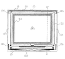
まず、本発明の第1実施形態における電気光学装置の画素部における構成について、図1から図4を参照して説明する。ここに図1は、電気光学装置の画像表示領域を構成するマトリクス状に形成された複数の画素における各種素子、配線等の等価回路である。図2は、データ線、走査線、画素電極等が形成されたTFTアレイ基板の相隣接する複数の画素群の平面図であり、図3は、図2のうち特にデータ線、シールド層及び画素電極の配置関係を示すためこれらの要素を抜き出して描いた平面図である。また、図4は、図2のA−A´断面図である。なお、図4においては、各層・各部材を図面上で認識可能な程度の大きさとするため、該各層・各部材ごとに縮尺を異ならしめてある。
(1st Embodiment)
First, the configuration of the pixel portion of the electro-optical device according to the first embodiment of the present invention will be described with reference to FIGS. Here, FIG. 1 is an equivalent circuit of various elements, wiring, and the like in a plurality of pixels formed in a matrix forming an image display area of the electro-optical device. FIG. 2 is a plan view of a plurality of pixel groups adjacent to each other on a TFT array substrate on which data lines, scanning lines, pixel electrodes, and the like are formed. FIG. FIG. 3 is a plan view of these elements extracted and drawn to show the arrangement relationship of electrodes. FIG. 4 is a sectional view taken along the line AA ′ of FIG. In FIG. 4, the scale of each layer / member is made different so that each layer / member has a size recognizable in the drawing.
図1において、本実施形態における電気光学装置の画像表示領域を構成するマトリクス状に形成された複数の画素には、それぞれ、画素電極9aと当該画素電極9aをスイッチング制御するためのTFT30とが形成されており、画像信号が供給されるデータ線6aが当該TFT30のソースに電気的に接続されている。データ線6aに書き込む画像信号S1、S2、…、Snは、この順に線順次に供給しても構わないし、相隣接する複数のデータ線6a同士に対して、グループ毎に供給するようにしてもよい。
In FIG. 1, a plurality of pixels formed in a matrix forming an image display area of the electro-optical device according to the present embodiment are each formed with a
また、TFT30のゲートに走査線3aが電気的に接続されており、所定のタイミングで、走査線3aにパルス的に走査信号G1、G2、…、Gmを、この順に線順次で印加するように構成されている。画素電極9aは、TFT30のドレインに電気的に接続されており、スイッチング素子であるTFT30を一定期間だけそのスイッチを閉じることにより、データ線6aから供給される画像信号S1、S2、…、Snを所定のタイミングで書き込む。
Also, the
画素電極9aを介して電気光学物質の一例としての液晶に書き込まれた所定レベルの画像信号S1、S2、…、Snは、対向基板に形成された対向電極との間で一定期間保持される。液晶は、印加される電圧レベルにより分子集合の配向や秩序が変化することにより、光を変調し、階調表示を可能とする。ノーマリーホワイトモードであれば、各画素の単位で印加された電圧に応じて入射光に対する透過率が減少し、ノーマリーブラックモードであれば、各画素の単位で印加された電圧に応じて入射光に対する透過率が増加され、全体として電気光学装置からは画像信号に応じたコントラストをもつ光が出射する。
The image signals S1, S2,..., Sn of a predetermined level written in the liquid crystal as an example of the electro-optical material via the
ここで保持された画像信号がリークするのを防ぐために、画素電極9aと対向電極との間に形成される液晶容量と並列に蓄積容量70を付加する。この蓄積容量70は、走査線3aに並んで設けられ、固定電位側容量電極を含むとともに定電位に固定された容量電極300を含んでいる。
In order to prevent the held image signal from leaking, a
以下では、上記データ線6a、走査線3a、TFT30等による、上述のような回路動作が実現される電気光学装置の、実際の構成について、図2ないし図4を参照して説明する。
Hereinafter, the actual configuration of the electro-optical device in which the above-described circuit operation is realized by the
まず、図2において、画素電極9aは、TFTアレイ基板10上に、マトリクス状に複数設けられており(点線部9a´により輪郭が示されている)、画素電極9aの縦横の境界に各々沿ってデータ線6a及び走査線3aが設けられている。データ線6aは、後述するようにアルミニウム膜等を含む積層構造からなり、走査線3aは、例えば導電性のポリシリコン膜等からなる。また、走査線3aは、半導体層1aのうち図中右上がりの斜線領域で示したチャネル領域1a´に対向するように配置されており、該走査線3aはゲート電極として機能する。すなわち、走査線3aとデータ線6aとの交差する箇所にはそれぞれ、チャネル領域1a´に走査線3aの本線部がゲート電極として対向配置された画素スイッチング用のTFT30が設けられている。
First, in FIG. 2, a plurality of
次に、電気光学装置は、図2のA−A´線断面図たる図4に示すように、例えば、石英基板、ガラス基板、シリコン基板からなるTFTアレイ基板10と、これに対向配置される、例えばガラス基板や石英基板からなる対向基板20とを備えている。
Next, as shown in FIG. 4, which is a cross-sectional view taken along the line AA ′ of FIG. 2, the electro-optical device is disposed to face the
TFTアレイ基板10の側には、図4に示すように、前記の画素電極9aが設けられており、その上側には、ラビング処理等の所定の配向処理が施された配向膜16が設けられている。画素電極9aは、例えばITO膜等の透明導電性膜からなる。他方、対向基板20の側には、その全面に渡って対向電極21が設けられており、その下側には、ラビング処理等の所定の配向処理が施された配向膜22が設けられている。このうち対向電極21は、上述の画素電極9aと同様に、例えばITO膜等の透明導電性膜からなり、前記の配向膜16及び22は、例えば、ポリイミド膜等の透明な有機膜からなる。このように対向配置されたTFTアレイ基板10及び対向基板20間には、後述のシール材(図16及び図17参照)により囲まれた空間に液晶等の電気光学物質が封入され、液晶層50が形成される。液晶層50は、画素電極9aからの電界が印加されていない状態で配向膜16及び22により所定の配向状態をとる。液晶層50は、例えば一種又は数種類のネマティック液晶を混合した電気光学物質からなる。シール材は、TFT基板10及び対向基板20をそれらの周辺で貼り合わせるための、例えば光硬化性樹脂や熱硬化性樹脂からなる接着剤であり、両基板間の距離を所定値とするためのグラスファイバー或いはガラスビーズ等のスペーサが混入されている。
As shown in FIG. 4, the
一方、TFTアレイ基板10上には、前記の画素電極9a及び配向膜16の他、これらを含む各種の構成が積層構造をなして備えられている。この積層構造は、図4に示すように、下から順に、下側遮光膜11aを含む第1層、TFT30及び走査線3a等を含む第2層、蓄積容量70及びデータ線6a等を含む第3層、シールド層400等を含む第4層、前記の画素電極9a及び配向膜16等を含む第5層(最上層)からなる。また、第1層及び第2層間には下地絶縁膜12が、第2層及び第3層間には第1層間絶縁膜41が、第3層及び第4層間には第2層間絶縁膜42が、第4層及び第5層間には第3層間絶縁膜43が、それぞれ設けられており、前述の各要素間が短絡することを防止している。また、これら各種の絶縁膜12、41、42及び43には、例えば、TFT30の半導体層1a中の高濃度ソース領域1dとデータ線6aとを電気的に接続するコンタクトホール等もまた設けられている。以下では、これらの各要素について、下から順に説明を行う。
On the other hand, on the
まず、第1層には、例えば、Ti(チタン)、Cr(クロム)、W(タングステン)、Ta(タンタル)、Mo(モリブデン)等の高融点金属のうちの少なくとも一つを含む、金属単体、合金、金属シリサイド、ポリシリサイド、これらを積層したもの等からなる下側遮光膜11aが設けられている。この下側遮光膜11aは、平面的にみて格子状にパターニングされており、これにより各画素の開口領域を規定している(図2参照)。下側遮光膜11aの走査線3aとデータ線6aが交差する領域では、画素電極9aの角を角取りするように突出した領域が形成されている。また、この下側遮光膜11aについては、その電位変動がTFT30に対して悪影響を及ぼすことを避けるために、画像表示領域からその周囲に延設して定電位源に接続するとよい。
First, the first layer includes, for example, a simple metal containing at least one of refractory metals such as Ti (titanium), Cr (chromium), W (tungsten), Ta (tantalum), and Mo (molybdenum). , An alloy, a metal silicide, a polysilicide, and a lower light-shielding
次に、第2層として、TFT30及び走査線3aが設けられている。TFT30は、図4に示すように、LDD(Lightly Doped Drain)構造を有しており、その構成要素としては、上述したようにゲート電極として機能する走査線3a、例えばポリシリコン膜からなり走査線3aからの電界によりチャネルが形成される半導体層1aのチャネル領域1a´、走査線3aと半導体層1aとを絶縁するゲート絶縁膜を含む絶縁膜2、半導体層1aにおける低濃度ソース領域1b及び低濃度ドレイン領域1c並びに高濃度ソース領域1d及び高濃度ドレイン領域1eを備えている。
Next, a
なお、TFT30は、好ましくは図4に示したようにLDD構造をもつが、低濃度ソース領域1b及び低濃度ドレイン領域1cに不純物の打ち込みを行わないオフセット構造をもってよいし、走査線3aの一部からなるゲート電極をマスクとして高濃度で不純物を打ち込み、自己整合的に高濃度ソース領域及び高濃度ドレイン領域を形成するセルフアライン型のTFTであってもよい。また、本実施形態では、画素スイッチング用TFT30のゲート電極を、高濃度ソース領域1d及び高濃度ドレイン領域1e間に1個のみ配置したシングルゲート構造としたが、これらの間に2個以上のゲート電極を配置してもよい。このようにデュアルゲート、あるいはトリプルゲート以上でTFTを構成すれば、チャネルとソース及びドレイン領域との接合部のリーク電流を防止でき、オフ時の電流を低減することができる。さらに、TFT30を構成する半導体層1aは非単結晶層でも単結晶層でも構わない。単結晶層の形成には、貼り合わせ法等の公知の方法を用いることができる。半導体層1aを単結晶層とすることで、特に周辺回路の高性能化を図ることができる。
The
以上説明した下側遮光膜11aの上、かつ、TFT30の下には、例えばシリコン酸化膜等からなる下地絶縁膜12が設けられている。下地絶縁膜12は、下側遮光膜11aからTFT30を層間絶縁する機能のほか、TFTアレイ基板10の全面に形成されることにより、TFTアレイ基板10の表面研磨時における荒れや、洗浄後に残る汚れ等で画素スイッチング用のTFT30の特性変化を防止する機能を有する。
Under the above-described lower light-shielding
そして、本実施形態においては特に、この下地絶縁膜12には、平面的にみて半導体層1aの両脇に、後述するデータ線6aに沿って延びる溝12cvが掘られており、この溝12cvに対応して、その上方に積層される走査線3aは下側に凹状に形成された部分を含んでいる(図2では、複雑化を避けるため不図示とした。)。また、この溝12cv全体を埋めるようにして、走査線3aが形成されていることにより、該走査線3aには、これと一体的に形成された水平的突出部3bが延設されるようになっている。これにより、TFT30の半導体層1aは、図2によく示されているように、平面的にみて側方から覆われるようになっており、少なくともこの部分からの光の入射が抑制されるようになっている。なお、水平的突出部3bは、半導体層1aの片側だけでもよい。
In the present embodiment, in particular, a groove 12cv extending along a
さて、前述の第2層に続けて第3層には、蓄積容量70及びデータ線6aが設けられている。蓄積容量70は、TFT30の高濃度ドレイン領域1e及び画素電極9aに電気的に接続された画素電位側容量電極としての第1中継層71と、固定電位側容量電極としての容量電極300とが、誘電体膜75を介して対向配置されることにより形成されている。この蓄積容量70によれば、画素電極9aにおける電位保持特性を顕著に高めることが可能となる。また、本実施形態に係る蓄積容量70は、図2の平面図を見るとわかるように、画素電極9aの形成領域にほぼ対応する光透過領域には至らないように形成されているため、換言すれば、遮光領域内に収まるように形成されている。すなわち、蓄積容量70は、隣接するデータ線6a間の走査線3aに重なる領域と、走査線3aとデータ線6aが交差する角部で下側遮光膜11が画素電極9aの角を角取りする領域に形成されている。これにより、電気光学装置全体の画素開口率は比較的大きく維持され、より明るい画像を表示することが可能となる。
Now, a
より詳細には、第1中継層71は、例えば導電性のポリシリコン膜からなり画素電位側容量電極として機能する。ただし、第1中継層71は、金属又は合金を含む単一層膜又は多層膜から構成してもよい。多層膜の場合は、下層を光吸収性の導電性のポリシリコン膜、上層を光反射性の金属又は合金にするとよい。また、この第1中継層71は、画素電位側容量電極としての機能のほか、コンタクトホール83、85及び89を介して、画素電極9aとTFT30の高濃度ドレイン領域1eとを中継接続する機能をもつ。この第1中継層71は、図2に示すように、後述する容量電極300の平面形状と略同一の形状を有するように形成されている。
More specifically, the
容量電極300は、蓄積容量70の固定電位側容量電極として機能する。第1実施形態において、容量電極300を固定電位とするためには、固定電位とされたシールド層400とコンタクトホール87を介して電気的接続が図られることによりなされている。
The
ただし、後述するように、容量電極300とデータ線6aとを別々の層として形成する形態では、好ましくは例えば、該容量電極300を、画素電極9aが配置された画像表示領域10aからその周囲に延設し定電位源と電気的に接続する等という手段をとることにより、該容量電極300を固定電位に維持するようにしてもよい。ちなみに、ここに述べた「定電位源」としては、データ線駆動回路101に供給される正電源や負電源の定電位源でもよいし、対向基板20の対向電極21に供給される定電位でも構わない。
However, in a mode in which the
そして、本実施形態では特に、この容量電極300と同一膜として、データ線6aが形成されている。ここに「同一膜」とは、同一層として、あるいは製造工程段階において同時に形成されていることを意味している。ただし、容量電極300及びデータ線6a間は平面形状的に連続して形成さているのではなく、両者間はパターニング上分断されている。
In the present embodiment, particularly, the
具体的には、図2に示すように、容量電極300は、走査線3aの形成領域に重なるように、すなわち図中X方向に沿って分断されつつ形成されており、データ線6aは、半導体層1aの長手方向に重なるように、すなわち図中Y方向に延在するように形成されている。より詳しくは、容量電極300は、走査線3aに沿って延びる本線部と、図2中、半導体層1aに隣接する領域において該半導体層1aに沿って図中上方に突出した突出部(図中略台形状のように見える部分)と、後述するコンタクトホール85に対応する個所が僅かに括れた括れ部とを備えている。このうち突出部は、蓄積容量70の形成領域の増大に貢献する。
Specifically, as shown in FIG. 2, the
他方、データ線6aは、図2中Y方向に沿って直線的に延びる本線部を有している。なお、半導体層1aの図2中上端にある高濃度ドレイン領域1eは、蓄積容量70の突出部の領域に重なるように、右方に90度直角に折り曲がるような形状を有しているが、これはデータ線6aを避けて、該半導体層1aと蓄積容量70との電気的接続を図るためである(図4参照)。
On the other hand, the
本実施形態では、以上のような形状が呈されるようにパターニング等が実施されて、容量電極300及びデータ線6aが同時に形成されることになる。
In the present embodiment, patterning or the like is performed so that the above-described shape is exhibited, and the
また、これら容量電極300及びデータ線6aは、図4に示すように、下層に導電性のポリシリコンからなる層、上層にアルミニウムからなる層の二層構造を有する膜として形成されている。このうちデータ線6aについては、後述する誘電体膜75の開口部を貫通するコンタクトホール81を介して、TFT30の半導体層1aと電気的に接続されることとなるが、該データ線6aが上述のような二層構造をとり、また前述の第1中継層71が導電性のポリシリコン膜からなることにより、該データ線6a及び半導体層1a間の電気的接続は、直接には、導電性のポリシリコン膜によって実現されることになる。すなわち、下から順に、第1中継層のポリシリコン膜、データ線6aの下層のポリシリコン膜及びその上層のアルミニウム膜ということになる。したがって、両者間の電気的接続を良好に保つことが可能となる。
Further, as shown in FIG. 4, the
また、容量電極300及びデータ線6aは、光反射性能に比較的優れたアルミニウムを含み、且つ、光吸収性能に比較的優れたポリシリコンを含むことから、遮光層として機能し得る。すなわち、これらによれば、TFT30の半導体層1aに対する入射光(図4参照)の進行を、その上側で遮ることが可能である。
Further, since the
誘電体膜75は、図4に示すように、例えば膜厚5〜200nm程度の比較的薄いHTO(High Temperature Oxide)膜、LTO(Low Temperature Oxide)膜等の酸化シリコン膜、あるいは窒化シリコン膜等から構成される。蓄積容量70を増大させる観点からは、膜の信頼性が十分に得られる限りにおいて、誘電体膜75は薄いほどよい。そして、本実施形態においては特に、この誘電体膜75は、図4に示すように、下層に酸化シリコン膜75a、上層に窒化シリコン膜75bというように二層構造を有し、TFTアレイ基板10の全面に渡って形成されている。なお、誘電体膜75の他の例として、下層の酸化シリコン膜75aは、TFTアレイ基板10の全面に渡って形成し、上層の窒化シリコン膜75bは、遮光領域(非開口領域)内で収まるようにパターンニングして、着色性のある窒化シリコン膜の存在により透過率が低くなることを防止するように構成してもよい。これにより、比較的誘電率の大きい窒化シリコン膜75bが存在することにより、蓄積容量70の容量値を増大させることが可能となる他、それにもかかわらず、酸化シリコン膜75aが存在することにより、蓄積容量70の耐圧性を低下せしめることがない。このように、誘電体膜75を二層構造とすることにより、相反する二つの作用効果を享受することが可能となる。また、窒化シリコン膜75bが存在することにより、TFT30に対する水の浸入を未然に防止することが可能となっている。これにより、本実施形態では、TFT30におけるスレッショルド電圧の上昇という事態を将来することがなく、比較的長期の装置運用が可能となる。なお、本実施形態では、誘電体膜75は、二層構造を有するものとなっているが、場合によっては、例えば酸化シリコン膜、窒化シリコン膜及び酸化シリコン膜等というような三層構造や、あるいはそれ以上の積層構造を有するように構成してもよい。
As shown in FIG. 4, the
また、本実施形態では、データ線6a及び容量電極300は、二層構造としたが、下層より、ポリシリコン膜、アルミニウム膜、窒化チタン膜の三層構造にし、窒化チタン膜をコンタクトホール87の開口時のバリアメタルとして形成しても良い。
In the present embodiment, the
以上説明したTFT30ないし走査線3aの上、かつ、蓄積容量70ないしデータ線6aの下には、例えば、NSG(ノンシリケートガラス)、PSG(リンシリケートガラス)、BSG(ボロンシリケートガラス)、BPSG(ボロンリンシリケートガラス)等のシリケートガラス膜、窒化シリコン膜や酸化シリコン膜等、あるいは好ましくはNSGからなる第1層間絶縁膜41が形成されている。そして、この第1層間絶縁膜41には、TFT30の高濃度ソース領域1dとデータ線6aとを電気的に接続するコンタクトホール81が開孔されている。また、第1層間絶縁膜41には、TFT30の高濃度ドレイン領域1eと蓄積容量70を構成する第1中継層71とを電気的に接続するコンタクトホール83が開孔されている。
Above the
なお、これら二つのコンタクトホールのうち、コンタクトホール81の形成部分では、前述の誘電体膜75が形成されないように、換言すれば、該誘電体膜75に開口部が形成されるようになっている。これは、該コンタクトホール81においては、第1中継層71を介して、高濃度ソース領域1b及びデータ線6a間の電気的導通を図る必要があるためである。ちなみに、このような開口部が誘電体膜75に設けられていれば、TFT30の半導体層1aに対する水素化処理を行うような場合において、該処理に用いる水素を、該開口部を通じて半導体層1aにまで容易に到達させることが可能となるという作用効果を得ることも可能となる。
Note that, of the two contact holes, in the portion where the
また、本実施形態では、第1層間絶縁膜41に対しては、約1000℃の焼成を行うことにより、半導体層1aや走査線3aを構成するポリシリコン膜に注入したイオンの活性化を図ってもよい。
In the present embodiment, the first
さて、前述の第3層に続けて第4層には、遮光性のシールド層400が形成されている。このシールド層400は、平面的にみると、図2及び図3に示すように、図2中X方向及びY方向それぞれに延在するように格子状に形成されている。該シールド層400のうち図2中Y方向に延在する部分については特に、データ線6aを覆うように、且つ、該データ線6aよりも幅広に形成されている。また、図2中X方向に延在する部分については、後述の第3中継電極402を形成する領域を確保するために、各画素電極9aの一辺の中央付近に切り欠き部を有している。さらには、図2中XY方向それぞれに延在するシールド層400の交差部分の角部においては、前述の容量電極300の略台形状の突出部に対応するように、略三角形状の部分が設けられている。シールド層400は、下側遮光膜11aと同じ幅でもよいし、下側遮光膜11aより幅が広くても、あるいは幅が狭くてもよい。
このシールド層400は、画素電極9aが配置された画像表示領域10aからその周囲に延設され、定電位源と電気的に接続されることで、固定電位とされている。なお、ここに述べた「定電位源」としては、データ線駆動回路101に供給される正電源や負電源の定電位源でもよいし、対向基板20の対向電極21に供給される定電位源でも構わない。
Now, a light-
The
このように、データ線6aの全体を覆うように形成されているとともに(図3参照)、固定電位とされたシールド層400の存在によれば、該データ線6a及び画素電極9a間に生じる容量カップリングの影響を排除することが可能となる。すなわち、データ線6aへの通電に応じて、画素電極9aの電位が変動するという事態を未然に回避することが可能となり、画像上に該データ線6aに沿った表示ムラ等を発生させる可能性を低減することができる。本実施形態においてはまた、シールド層400は格子状に形成されているから、走査線3aが延在する部分についても無用な容量カップリングが生じないように、これを抑制することが可能となっている。また、シールド層400における上述の三角形状の部分は、容量電極300と画素電極9aとの間に生じる容量カップリングの影響を排除することが可能であり、これによっても、上述と略同様な作用効果が得られることになる。
As described above, the capacitance formed between the
また、第4層には、このようなシールド層400と同一膜として、本発明にいう「中継層」の一例たる第2中継層402が形成されている。この第2中継層402は、後述のコンタクトホール89を介して、蓄積容量70を構成する第1中継層71及び画素電極9a間の電気的接続を中継する機能を有する。なお、これらシールド層400及び第2中継層402間は、前述の容量電極300及びデータ線6aと同様に、平面形状的に連続して形成されているのではなく、両者間はパターニング上分断されるように形成されている。
In the fourth layer, a
他方、上述のシールド層400及び第2中継層402は、下層にアルミニウムからなる層、上層に窒化チタンからなる層の二層構造を有している。これにより、まず、窒化チタンによる水分防止作用の発揮が期待される。また、第2中継層402において、下層のアルミニウムからなる層は、蓄積容量70を構成する第1中継層71と接続され、上層の窒化チタンからなる層は、ITO等からなる画素電極9aと接続されるようになっている。この場合、とりわけ後者の接続は良好に行われることになる。この点、仮に、アルミニウムとITOとを直接に接続してしまう形態をとると、両者間において電蝕が生じてしまい、アルミニウムの断線、あるいはアルミナの形成による絶縁等のため、好ましい電気的接続が実現されないこととは対照的である。また、窒化チタンは、コンタクトホール89の開口時の突きぬけ防止のためのバリアメタルとして機能する。このように、本実施形態では、第2中継層402と画素電極9aとの電気的接続を良好に実現することができることにより、該画素電極9aに対する電圧印加、あるいは該画素電極9aにおける電位保持特性を良好に維持することが可能となる。
On the other hand, the above-mentioned
さらには、シールド層400及び第2中継層402は、光反射性能に比較的優れたアルミニウムを含み、且つ、光吸収性能に比較的優れた窒化チタンを含むことから、遮光層として機能し得る。すなわち、これらによれば、TFT30の半導体層1aに対する入射光(図2参照)の進行を、その上側でさえぎることが可能である。なお、このようなことについては、既に述べたように、上述の容量電極300及びデータ線6aについても同様にいえる。本実施形態においては、これらシールド層400、第2中継層402、容量電極300及びデータ線6aが、TFTアレイ基板10上に構築される積層構造の一部をなしつつ、TFT30に対する上側からの光入射を遮る上側遮光膜(あるいは、「積層構造の一部」を構成しているという点に着目すれば「内蔵遮光膜」)として機能しうる。なお、この「上側遮光膜」ないし「内蔵遮光膜」なる概念によれば、上述の構成のほか、走査線3aや第1中継層71等もまた、それに含まれるものとして考えることができる。要は、最も広義に解する前提の下、TFTアレイ基板10上に構築される不透明な材料からなる構成であれば、「上側遮光膜」ないし「内蔵遮光膜」と呼びうる。
Further, since the
以上説明した前述のデータ線6aの上、かつ、シールド層400の下には、NSG、PSG、BSG、BPSG等のシリケートガラス膜、窒化シリコン膜や酸化シリコン膜等、あるいは好ましくはNSGからなる第2層間絶縁膜42が形成されている。この第2層間絶縁膜42には、前記のシールド層400と容量電極300とを電気的に接続するためのコンタクトホール87、及び、第2中継層402と第1中継層71とを電気的に接続するためのコンタクトホール85がそれぞれ開孔されている。
Above the above-described
なお、第2層間絶縁膜42に対しては、第1層間絶縁膜41に関して前述したような焼成を行わないことにより、容量電極300の界面付近に生じるストレスの緩和を図るようにしてもよい。
In addition, the stress generated near the interface of the
最後に、第5層には、上述したように画素電極9aがマトリクス状に形成され、該画素電極9a上に配向膜16が形成されている。この画素電極9aは、角部がカットされた形状でもよい。そして、この画素電極9a下には、NSG、PSG、BSG、BPSG等のシリケートガラス膜、窒化シリコン膜や酸化シリコン膜等、あるいは好ましくはBPSGからなる第3層間絶縁膜43が形成されている。この第3層間絶縁膜43には、画素電極9a及び前記の第2中継層402間を電気的に接続するためのコンタクトホール89が開孔されている。また、本実施形態では特に、第3層間絶縁膜43の表面は、CMP(Chemical Mechanical Polishing)処理等により平坦化されており、その下方に存在する各種配線や素子等による段差に起因する液晶層50の配向不良を低減する。ただし、このように第3層間絶縁膜43に平坦化処理を施すのに代えて、又は加えて、TFTアレイ基板10、下地絶縁膜12、第1層間絶縁膜41及び第2層間絶縁膜42のうち少なくとも一つに溝を掘って、データ線6a等の配線やTFT30等を埋め込むことにより、平坦化処理を行ってもよい。
Finally, in the fifth layer, the
以上のような構成となる第1実施形態の電気光学装置では、大きく、次のような三つの作用効果が奏される。すなわち、第一に、TFTアレイ基板10上の積層構造中にシールド層400が形成されていることにより、画素電極9a及びデータ線6a間の容量カップリングの影響を排除することが可能である。すなわち、該シールド層400は、画像表示領域10a外に設けられた定電位源に接続等されて固定電位とされるとともに、データ線6aを覆うように形成されているため、データ線6aの通電により、画素電極9aの電位が変動するという事態を未然に回避することができる。したがって、第1実施形態によれば、データ線6aに沿った画像上の表示ムラ等を発生させることが殆どない。
In the electro-optical device according to the first embodiment having the above-described configuration, the following three effects can be obtained. That is, first, since the
第二に、シールド層400が窒化チタンを含んでいたことにより、TFT30の耐湿性を向上させることが可能となる。これは、該窒化チタンを含む窒化物は、一般に、その構造が稠密であり、水分の浸入ないし拡散をせき止める作用に優れていることによる。したがって、第1実施形態によれば、TFT30の高寿命化を図ることができ、また、電気光学装置全体の比較的長期の運用が可能となる。
Second, since the
第三に、画素電極9aとTFT30とを電気的に接続するための構成として、第1実施形態では、第2中継層402が形成されていたことにより、該画素電極9aを構成するITOによる電蝕発生の危険性を回避することができる。特に、この第2中継層402は、前記のシールド層400と同一膜として形成されていることから、該第2中継層402は、ITOとより電蝕の生じにくい窒化チタンを含んでいる。したがって、第1実施形態によれば、画素電極9a及びTFT30間の電気的接続が断絶されるという事態を未然に回避することが可能となり、該画素電極9aの良好な駆動を実現することができる。
Third, as a configuration for electrically connecting the
そして、第1実施形態では更に、上述のシールド層400及び第2中継層402に関して、次のような付随的な作用効果が奏されることとなる。
Further, in the first embodiment, the following additional operation and effect can be achieved with respect to the
すなわち、第1実施形態では、データ線6aは蓄積容量70を構成する容量電極300と同一膜として形成されていた。したがって、前述のような作用効果を発揮するシールド層400を画素電極9a及びデータ線6a間に配置する構成を採るに際し、第1実施形態では、該シールド層400のために別の層を新たに設ける必要がない。すなわち、積層構造の高層化を防止することが可能となる。これにより、製造容易性の確保や製造歩留まり率を高く維持することが可能となる。
That is, in the first embodiment, the
また、同じ理由により、前述の第2中継層402の配置も無理なく行うことができる。すなわち、データ線6aが容量電極300と同一膜として形成されているのであれば、該容量電極300と画素電極9a間に第2中継層402を設けることは自然に行われ得るのである。
Further, for the same reason, the above-described arrangement of the
さらに、データ線6aがアルミニウム膜及び導電性ポリシリコン膜という二層構造をとることにより、既に述べたように、該データ線6a及びTFT30間の電気的接続を良好に図ることができる。
Further, as described above, the
以上のように、第1実施形態によれば、画素電極9a及びデータ線6a間の容量カップリングの影響を排除するとともに、TFT30の長寿命化が図られ、画素電極9a及び第2中継層402、ひいてはTFT30間の電気的接続、あるいはデータ線6a及びTFT30間の電気的接続を良好に実現することができるから、従前にも増して、より高品質な画像を表示することが可能となる。
As described above, according to the first embodiment, the effect of the capacitive coupling between the
(第2実施形態)
次に、本発明の第2実施形態の電気光学装置について、図5から図8を参照しながら説明する。ここに図5は、図2と同趣旨の図であって、シールド層及びデータ線等の構成について異なる態様となるものを示すものであり、図6は、図4と同趣旨の図であって図5のA−A´断面図であり、データ線及びシールド層等の構成について異なる態様となるものを示すものである。また、図7は、データ線上に形成される窒化膜の態様を示す平面図であり、図8は、図5のB−B´断面図であり、図9は、図8の変形形態に係る図である。なお、第2実施形態の電気光学装置は、上記の第1実施形態の電気光学装置の画素部における構成と略同様な構成を備えている。したがって、以下では、第2実施形態において特徴的な部分のみについて主な説明を加えることとし、残余の部分については、その説明を適宜省略ないし簡略化することとする。
(2nd Embodiment)
Next, an electro-optical device according to a second embodiment of the present invention will be described with reference to FIGS. FIG. 5 is a diagram having the same purpose as FIG. 2 and shows a different configuration of the shield layer and the data line, and FIG. 6 is a diagram having the same purpose as FIG. FIG. 6 is a sectional view taken along the line AA ′ of FIG. FIG. 7 is a plan view showing an aspect of the nitride film formed on the data line, FIG. 8 is a cross-sectional view taken along the line BB ′ of FIG. 5, and FIG. FIG. The electro-optical device according to the second embodiment has a configuration substantially similar to the configuration of the pixel portion of the electro-optical device according to the first embodiment. Therefore, in the following, only the main features of the second embodiment will be mainly described, and the description of the remaining portions will be omitted or simplified as appropriate.
第2実施形態では、図6に示すように、図4と比べて、蓄積容量70を構成する上部電極たる容量電極300とデータ線6aとが同一膜として構成されていない点、また、それに伴って、層間絶縁膜が増加されている。すなわち、新たにもう一層、「第4層間絶縁膜44」が設けられている点、そしてゲート電極3aaと同一膜として中継電極719が形成されている点に大きな相違がある。これにより、TFTアレイ基板10上から順に、走査線を兼ねる下側遮光膜11aを含む第1層、ゲート電極3aaを有するTFT30を含む第2層、蓄積容量70を含む第3層、データ線6a等を含む第4層、シールド層404が形成される第5層、前記の画素電極9a及び配向膜16等を含む第6層(最上層)からなる。また、第1層及び第2層間には下地絶縁膜12が、第2層及び第3層間には第1層間絶縁膜41が、第3層及び第4層間には第2層間絶縁膜42が、第4層及び第5層間には第3層間絶縁膜43が、第5層及び第6層間には第4層間絶縁膜44が、それぞれ設けられており、前述の各要素間が短絡することを防止している。本例では、第1実施形態における第2層には走査線3aが形成されていたのに代えて、第2実施形態では、走査線3aに代わるゲート電極3aaが形成されるとともに、これと同一膜として中継電極719が新たに形成されている。以下、各層における構成について、より詳しく説明する。
In the second embodiment, as shown in FIG. 6, as compared with FIG. 4, the point that the
まず、第2層には、半導体層1aのチャネル領域1a´に対向するように、ゲート電極3aaが形成されている。このゲート電極3aaは、第1実施形態の走査線3aのように線状には形成されておらず、半導体層1aないしチャネル領域1a´がTFTアレイ基板10上に島状に形成されていることに応じて、島状に形成されている。また、第2実施形態では、これに応じて、コンタクトホール成す溝12cvの底が、第1層の下側遮光膜11aの表面に接する深さを有しているとともに、該下側遮光膜11aは図5中X方向に延在するストライプ状に形成されている。これにより、溝12cv上に形成されたゲート電極3aaは、該溝12cvを介して下側遮光膜11aと電気的に接続されることになる。すなわち、第2実施形態では、ゲート電極3aaには、下側遮光膜11aを通じて走査信号が供給されるようになっている。換言すれば、第2実施形態の下側遮光膜11aは、走査線としての機能を担うことになる。
First, a gate electrode 3aa is formed in the second layer so as to face the
なお、第2実施形態における下側遮光膜11aについては、図5に示すように、データ線6aが延在する方向に沿って突出部を有している。これにより、第2実施形態の下側遮光膜11aは、第1実施形態における格子状の下側遮光膜11aと遜色ない遮光機能をも発揮することになる。ただし、相隣接する下側遮光膜11aから延びる突出部は相互に接触することはなく、互いに電気的に絶縁されている。こうしないと、下側遮光膜11aを、走査線として機能させることができないからである。また、下側遮光膜11aは、データ線6aと交差する領域では、画素電極9aの角を角取りするように突出した領域が形成されている。そして、下側遮光膜11aは、TFT30、走査線3a、データ線6a、蓄積容量70、シールド用中継層6a1、第2中継層6a2、第3中継層406を、下側から見て覆うように形成されている。
As shown in FIG. 5, the lower light-shielding
そして、第2実施形態においては特に、上述のゲート電極3aaと同一膜として中継電極719が形成されている。中継電極719は、平面的に見て、図5に示すように、各画素電極9aの一辺の略中央に位置するように、島状に形成されている。中継電極719と、ゲート電極3aaとは同一膜として形成されているから、後者が例えば導電性ポリシリコン膜等からなる場合においては、前者もまた、導電性ポリシリコン膜等からなる。
In the second embodiment, in particular, the
次に、第3層には、蓄積容量70を構成する第1中継層71、誘電体膜75及び容量電極300が形成されている。このうち第1中継層71はポリシリコンで形成される。そして、容量電極300は、もはやデータ線6aと同時に形成されるわけではないので、第1実施形態のように、該データ線6a及びTFT30間の電気的接続に対する配慮を払う意味を込めて、アルミニウム膜及び導電性のポリシリコン膜という二層構造をとる必要は必ずしもない。したがって、該容量電極300は、例えば、下側遮光膜11aと同様に、Ti、Cr、W、Ta、Mo等の高融点金属のうちの少なくとも一つを含む、金属単体、合金、金属シリサイド、ポリシリサイド、これらを積層したもの等の遮光性材料から構成するとよい。これによれば、容量電極300は、上述の「上側遮光膜」ないし「内蔵遮光膜」としての機能をよりよく発揮し得る。
Next, in the third layer, the
また、同じ理由、すなわち容量電極300とデータ線6aとが別々の層に形成されることにより、本態様では、同一平面内における両者間の電気的絶縁を図る必要はない。したがって、容量電極300は、走査線3aの方向に延在する容量線の一部として形成することが可能である。
この蓄積容量70は、TFT30とデータ線6aとの間に形成されるので、図5に示すように、走査線3aの延設方向並びにデータ線6aの延設方向に十字形状に形成されている。これにより、蓄積容量を増大化でき、遮光性の容量電極300により、TFT30への遮光性を高めることができる。また、蓄積容量70は、下側遮光膜11やシールド層400が形成されている画素電極6aの角部に形成すると、より蓄積容量の増大化、遮光性を高めることができる。
Further, for the same reason, that is, since the
Since this
以上述べた、ゲート電極3aa及び中継電極719の上、且つ、蓄積容量70の下には、第1層間絶縁膜41が形成されているが、該第1層間絶縁膜41は、上述と略同様に、NSG、PSG、BSG、BPSG等のシリケートガラス膜、窒化シリコン膜や酸化シリコン膜等で構成すればよい。また、この第1層間絶縁膜41には、第1中継層71の図6中下面に電気的接続点をもつように配置された、コンタクトホール881が開孔されている。これにより、第1中継層71及び中継電極719間の電気的接続が図られることになる。また、第1層間絶縁膜41には、後述する第2中継層6a2との電気的接続を図るため、後記第2層間絶縁膜42をも貫通するように開孔されたコンタクトホール882が開孔されている。
As described above, the first
他方、第4層にはデータ線6aが形成されるが、該データ線6aもまた、前述の容量電極300と同様に、二層構造をとる必要は必ずしもない。例えば、該データ線6aは、アルミニウム単体、あるいはアルミニウム合金その他の金属又は合金等の導電性材料で構成すればよい。ただし、このデータ線6aは、TFT30の半導体層1aと電気的に接触しなければならないことは、上記第1実施形態と変わりないから、該半導体層1aと直接的に接触する部分については、導電性ポリシリコン膜が設けられていることが好ましい。図6においては、第1中継層71と同一膜として形成された膜が、コンタクトホール81内に形成されていることにより、上のような要請は満たされている。
On the other hand, although the
そして、第2実施形態では特に、上述のようにアルミニウム等から構成されたデータ線6aの上に、かつ、該データ線6aに沿って、例えばSiN膜、SiON膜又はTiN膜等からなる窒化膜401を備えている。ただし、本実施形態に係る窒化膜401は、データ線6a上の他、マトリクス状に配列された画素電極9a並びにこれらの間隙を縫うように配置されたデータ線6a及び走査線3aが形成される領域として規定される画像表示領域10aの周囲にも、ロの字状に形成されている。なお、この窒化膜401の厚さは、例えば10〜100nm程度、より好ましくは10〜30nm程度に構成するとよい。
In the second embodiment, in particular, a nitride film made of, for example, a SiN film, a SiON film, a TiN film, or the like is formed on and along the
以上により、本実施形態に係る窒化膜401は、TFTアレイ基板10上において、全体的に図7に概略的に示すような形状で形成されていることになる。なお、図7中、画像表示領域10aの周囲に存在している窒化膜401は、後述するデータ線駆動回路101や走査線駆動回路104を構成するCMOS(Complementary MOS)型TFTに対する水分浸入防止に大きく貢献する(図16参照)。ただし、窒化物は、その他一般の材料に比べて、ドライエッチング等におけるエッチングレートが小さくなることが予測されるから、上述の画像表示領域10aの周囲の領域に窒化膜401を形成する場合であって、該領域内にコンタクトホール等を形成する必要がある場合においては、該窒化膜401内に、該コンタクトホールの位置に対応した孔を予め形成しておくとよい。これは、図7に示すようなパターニングを実施する際に併せて行っておけば、製造工程の簡略化に資する。
As described above, the
また、第4層には、データ線6aと同一膜として、シールド層用中継層6a1及び第2中継層6a2(ただし、第1実施形態における「第2中継層」とは少々意味合いが異なる。)が形成されている。このうち前者は、遮光性のシールド層404と容量電極300とを電気的に接続するための中継層であり、後者は、画素電極9aと第1中継層71とを電気的に接続するための中継層である。なお、これらは、データ線6aと同一材料により構成されることとなるのはいうまでもない。
In the fourth layer, the same layer as the
以上述べた、蓄積容量70の上、且つ、データ線6a、シールド用中継層6a1及び第2中継層6a2の下には、第2層間絶縁膜42が形成されているが、該第2層間絶縁膜42は、上述と略同様に、NSG、PSG、BSG、BPSG等のシリケートガラス膜、窒化シリコン膜や酸化シリコン膜等で構成すればよい。
また、この第2層間絶縁膜42には、前述のシールド層用中継層6a1及び第2中継層6a2に対応するように、コンタクトホール801及び前記のコンタクトホール882が開孔されている。
As described above, the second
In the second
次に、第5層には、遮光性のシールド層404が形成されている。これは例えば、上述のシールド層400と同様に、上層に窒化チタンからなる層、下層にアルミニウムからなる層という二層構造で構成してもよいし、また、場合により、ITOその他の導電性材料で構成してもよい。このシールド層404は、前述のシールド層用中継層6a1を介して、容量電極300と電気的に接続されている。これにより、シールド層404は固定電位とされており、上記第1実施形態と同様に、画素電極9a及びデータ線6a間に生じる容量カップリングの影響を排除する。遮光性のシールド層400は、下側遮光膜11aと同じ幅でもよいし、下側遮光膜11aより幅が広くても、あるいは幅が狭くてもよい。ただし、第3中継層406を除いて、TFT30、走査線3a、データ線6a、蓄積容量70を上側から見て覆うように形成されている。そして、シールド層400と下側遮光膜11とで、画素開口領域の角部、すなわち4つの角部、画素開口領域の各辺を規定することになる。
また、この第5層には、シールド層404と同一膜として、第3中継層406が形成されている。
Next, a light-
Further, a
以上述べた、データ線6aの上、且つ、シールド層404の下には、第3層間絶縁膜43が形成されている。この第3層間絶縁膜43を構成する材料等についても、上記の第2層間絶縁膜42と同様でよい。ただし、データ線6a等が、上述のようにアルミニウム等を含む場合においては、これを高温環境下に曝すことを避けるため、該第3層間絶縁膜43は、好ましくはプラズマCVD法等の低温成膜法を用いて形成することが好ましい。
The third
また、この第3層間絶縁膜43には、シールド層404と前述のシールド層用中継層6a1とを電気的に接続するためのコンタクトホール803が形成されており、前述の第2中継層6a2へと通じており、第3中継層406に対応するコンタクトホール804が形成されている。
In the third
残る構成は、第6層には画素電極9a及び配向膜16が形成されるとともに、該第6層及び第5層間には第4層間絶縁膜44が形成されており、該第4層間絶縁膜44には、画素電極9aと第3中継層406とを電気的に接続するためのコンタクトホール89が開孔されている、というものになっている。
The remaining configuration is such that the
なお、上述の構成において、第3中継層406については、ITO等からなる画素電極9aと直接的に接触することとなるから、上述した電蝕に注意すべきである。したがって、これを考慮すれば、シールド層404及び第3中継層406は、第1実施形態と同様に、アルミニウム及び窒化チタンからなる二層構造とすることが好ましい。また、シールド層404及び第3中継層406をITOから構成するのであれば、該第3中継層406と画素電極9aとの電蝕発生について心配する必要はないが、シールド層404及びシールド層用中継層6a1間、あるいは第3中継層406及び第2中継層6a2間における電蝕発生について心配する必要がある。したがって、この場合においてはITO及びアルミニウムの直接的な接触を避けるべく、シールド層用中継層6a1、第2中継層6a2、ひいてはデータ線6aについて、適当な二層構造を採用することが好ましい。
In the above-described configuration, the
あるいは、第2実施形態においては、上述のように、容量電極300は容量線の一部として構成可能であるから、該容量電極300を固定電位とするためには、該容量線を画像表示領域10a外まで延設して定電位源に接続するような形態とすればよい。この場合更に、容量電極300を含む容量線は、それ自体独自に定電位源に接続することが可能であり、シールド層404もまた、それ自体独自に定電位源に接続することが可能となるため、そのような構成を採用する場合においては、両者間を電気的に接続するコンタクトホール801及び803を設ける必要はなくなる。よって、この場合においては、シールド層404及び容量電極300を構成する材料選択や、シールド層用中継層6a1の材料選択を行う際に(そもそも当該シールド用中継層6a1はもはや不要である。)、「電蝕」の発生に配慮する必要はない。
Alternatively, in the second embodiment, as described above, since the
以上のような構成となる第2実施形態の電気光学装置においては、まず、上述の第1実施形態におけるのと略同様な作用効果が奏されることが明白である。すなわち、第1実施形態と同様に、シールド層404の存在により画素電極9a及びデータ線6a間の容量カップリングの影響を排除することが可能であり、また、第3中継層406の存在により、画素電極9aを構成するITOによる電蝕発生の危険性を回避することが可能である。
In the electro-optical device according to the second embodiment having the above-described configuration, first, it is apparent that substantially the same operation and effect as those in the above-described first embodiment are exerted. That is, as in the first embodiment, the presence of the
そして、第2実施形態では特に、データ線6a上、かつ、画像表示領域10aの周囲の上に、窒化膜401が形成されていたことにより、TFT30の耐湿性を更に向上することが可能となる。すなわち、窒化膜ないし窒化物は、既に述べたように、水分の浸入ないし拡散をせき止める作用に優れているから、TFT30の半導体層1aに対する水分浸入を未然に防止することが可能となるのである。第2実施形態では、この他、シールド層404、第3中継層406等や蓄積容量70を構成する誘電体膜75において、窒化膜が用いられ得るが、これらすべての構成について、そのような窒化膜を備えれば、水分浸入防止作用はより効果的に発揮されることになる。ただし、すべてに「窒化膜」を設けない形態としてよいことは勿論である。
In the second embodiment, in particular, since the
また、第2実施形態において、窒化膜401は、第4層において、画像表示領域10a外の領域をのぞいて、データ線6a上にのみ存在することから、大きな内部応力が集中するようなことがなく、窒化膜401自身がその内部応力によって破壊するに至ったり、また、その応力が外部に作用することによって、窒化膜401の周囲に存在する、例えば第3層間絶縁膜43等にクラックを生じさせるようなことがない。このようなことは、窒化膜がTFTアレイ基板10上の全面に設けられている場合を仮に想定するとより明白である。
In the second embodiment, since the
さらには、第2実施形態における窒化膜401は、その厚さが10〜100nm程度、より好ましくは10〜30nm程度と比較的小さくされていることから、上述のような作用効果は更に効果的に享受され得ることになる。
Furthermore, since the
更に加えて、第2実施形態では特に、中継電極719が設けられていたことにより、次のような作用効果を得ることができる。すなわち、図4においては、TFT30及び画素電極9a間の電気的接続を図るためには、同図におけるコンタクトホール85のように、蓄積容量70を構成する、より下層の電極たる第1中継層71の図中「上面」において接触を図る必要があった。
In addition, in the second embodiment, in particular, since the
しかしながら、このような形態では、容量電極300及び誘電体膜75の形成工程において、それらの前駆膜をエッチングする際には、その直下に位置する第1中継層71を健全に残存させながら、当該前駆膜のエッチングを実行するという非常に困難な製造工程を実施しなければならない。とりわけ本発明のように、誘電体膜75として高誘電率材料を使用する場合においては、一般にそのエッチングが困難であり、また、容量電極300におけるエッチングレートと該高誘電率材料におけるエッチングレートが不揃いになるなどの条件も重なるため、当該製造工程の困難性はより高まることになる。したがって、このような場合においては、第1中継層71において、いわゆる「突き抜け」等を生じさせてしまう可能性が大きい。こうなると、悪い場合には、蓄積容量70を構成する容量電極300及び第1中継層71間に短絡を生じさせるおそれ等も生じてくる。
However, in such a mode, in the step of forming the
しかるに、本形態のように、中継電極719を設けることで、第1中継層71の図中「下面」に電気的接続点をもたせることによって、TFT30及び画素電極9a間の電気的接続を実現するようにすれば、上述のような不具合は発生しないのである。なぜなら、図6からも明らかな通り、本形態では、容量電極300及び誘電体膜75の前駆膜をエッチングしつつ、第1中継層71を残存させなければならないという工程は必要ないからである。
However, by providing the
尚、誘電体膜75は、図6に示すように、下層に酸化シリコン膜75a、上層に窒化シリコン膜75bというように二層構造を有し、TFTアレイ基板10の全面に渡って形成されている。また、誘電体膜75の他の例として、下層の酸化シリコン膜75aは、TFTアレイ基板10の全面に渡って形成し、上層の窒化シリコン膜75bは、遮光領域(非開口領域)内で収まるようにパターンニングして、着色性のある窒化シリコン膜の存在により透過率が低くなることを防止するように構成してもよい。
As shown in FIG. 6, the
以上により、本形態によれば、上述のような困難なエッチング工程を経る必要がないから、第1中継層71及び画素電極9a間の電気的接続を良好に実現することができる。これは、中継電極719を介して両者間の電気的接続を実現しているからに他ならない。更にいえば、同じ理由から、本形態によれば、容量電極300及び第1中継層71間で短絡が生じるなどという可能性はきわめて小さい。すなわち、欠陥なき蓄積容量70を好適に形成することが可能なのである。
As described above, according to the present embodiment, it is not necessary to go through the difficult etching process as described above, so that the electrical connection between the
なお、第2実施形態では、上述した水分浸入防止に係る作用効果、あるいはその他の有用な作用効果を得るために、以下に述べる各種の変形形態をとることが可能である。 In the second embodiment, various modifications described below can be taken in order to obtain the above-described effects relating to the prevention of moisture penetration or other useful effects.
第一は、上述のデータ線6a及び該データ線6a上の窒化膜401の幅と、下側遮光膜11aの幅との関係を好適に設定することに関連する。まず、窒化膜401の幅をW1、データ線6aの幅をW2、下側遮光膜11aの幅をW3とすれば、W2<W1≦W3なる関係が満たされることが好ましい。この場合、当該構成は、図5のB−B´断面図たる図8に示すような構造を有していることになる。この図8において、既に述べたように、窒化膜401は、その幅W1が、データ線6aの幅W2よりも大きく、かつ、下側遮光膜11aの幅W3と同等ないしはそれよりも小さく形成されている。このことは、窒化膜401の縁が、光透過領域に至らないことを意味する。図8では、下側遮光膜11aの幅W3に対応する図中左右両側の位置に、光透過領域とそうでない領域とを画す一点鎖線が描かれているが、窒化膜401は、右側(又は左側)の一点鎖線を越えて更に右側(又は左側)には存在していない。つまり、窒化膜401の縁は、光透過領域には至っていないのである。したがって、このような形態によれば、電気光学装置全体の透過率を減少せしめるような事態を回避することができ、より明るい高品質な画像の表示が可能となる。なお、上述の場合において、窒化膜401は、データ線6aよりもその両側につきそれぞれ0.1〜0.5μmだけ大きく(つまり、(W1−W2)/2=0.1〜0.5μmである。)するようにすると好ましい。
The first relates to suitably setting the relationship between the
なお、図8(及びすぐ後に参照する図9)においては、対向基板20側の構成も示されており、該対向基板20上には、対向電極21、配向膜22が形成されているほか、対向基板側遮光膜23が形成されていることが示されている。この対向基板側遮光膜23は、前記の下側遮光膜11aと同様に、例えばTi、Cr、W、Ta、Mo等の高融点金属のうちの少なくとも一つを含む、金属単体、合金、金属シリサイド、ポリシリサイド、これらを積層したもの、あるいは樹脂ブラック等からなり、格子状にパターニングされた遮光膜である。また、本形態においては、図に示すように下側遮光膜11aの幅W3と同一の幅W3を有するものとして形成されている。
FIG. 8 (and FIG. 9 to be referred to immediately after) also shows the configuration on the
この対向基板側遮光膜23により、画素間の光の混合はより確実に防止されることとなり、また、TFT30に対する光遮蔽効果も相応に発揮されることが期待される。なお、上述では、下側遮光膜11aの幅と対向基板側遮光膜23の幅とは同一とされていたが、前者は後者よりも小さくしてもよい。このようにすれば、電気光学装置内部に斜めから進入した光が反射等することを未然に防止することができ、TFT30に対する遮光性能をより向上させることが可能となる。
The opposing substrate side light-shielding
次に、前記のW2<W1≦W3に代えて、W2<W1且つW3<W1なる関係が満たされるようにしても好ましい。この場合、当該構成は、図8と同趣旨の図である図9に示すような構造を有していることになる。この図9において、既に述べたように、窒化膜401´は、その幅W1が、データ線6aの幅W2よりも大きく、かつ、下側遮光膜11aの幅W3と比べても大きく形成されている。これにより、このような形態では、窒化膜401´が光透過領域にまで至るように形成されることになる。しかしながら、W3−W2の大きさが然程大きなものにさえならなければ、光透過率には実質的には影響を及ぼさない範囲が考えられることから、このような形態としても画像の明るさを必ずしも損なうわけではない。
Next, it is preferable that the relationships W2 <W1 and W3 <W1 be satisfied instead of the above-mentioned W2 <W1 ≦ W3. In this case, the configuration has a structure as shown in FIG. 9, which has the same effect as FIG. In FIG. 9, as described above, the nitride film 401 'is formed such that its width W1 is larger than the width W2 of the
そして、このような形態では特に、図10に示すように、画像上のフリッカを減少させることが可能となるのである。ここに図10は、突出値P=(W1−W2)/2の変化に応じて、完成した電気光学装置により表示された画像上に現れるフリッカの程度がどのように変化するかを示したグラフである。この図に示すように、従来例(図10中の左軸上)、すなわちデータ線6aに窒化膜が存在しない場合に比べて、本形態に係る窒化膜401が形成されている場合には、画像上のフリッカが低減されている様子がわかる。そして、その低減の度合いは、突出値Pの増加に応じて、より大きくなっていることもわかる。すなわち、突出値Pが大きくなる程フリッカは低減する。その正確な理由は明らかではないが、窒化膜401が固有に有する屈折率が、データ線6aの脇を通る入射光を屈折させるためであると考えられる。すなわち、窒化膜401の比較的幅広の部分に入射した光は、該部分によって屈折してその進行経路を変え、本来であればTFT30に入射するはずであった光を、どこか別の箇所へと至らしめることとなると考えられるのである。そうすると、TFT30に対する入射光は減少することとなるから、光リーク電流が減少し、これによりフリッカが減少したものと考えられる。
In particular, in such an embodiment, as shown in FIG. 10, flicker on the image can be reduced. Here, FIG. 10 is a graph showing how the degree of flicker appearing on an image displayed by the completed electro-optical device changes according to the change of the protrusion value P = (W1−W2) / 2. It is. As shown in this figure, when the
さらに、上述のいずれの場合においても、窒化膜401の幅W1は、データ線6aの幅W2よりも大きくされている。W1>W2、あるいは前記の突出値Pが0でない値をとることから、該窒化膜401の製造段階において、次のような作用効果も得られる。すなわち、該窒化膜401の製造段階においては、通常、その元となる膜を基板上の全面に形成した後、フォトリソグラフィ及びエッチング工程によってデータ線6a上のみ、あるいはこれに加えて画像表示領域10aの周囲を含むような形状の窒化膜401がパターニングで成形されることになるが、この際、エッチング工程が行われることにより、データ線6aに無用なダメージを与える可能性があるのである。しかるに、(窒化膜401の幅W1)>(データ線6aの幅W2)という関係が満たされていれば、上述のエッチングによって与えられるダメージは、当該窒化膜401の縁によって受け持たせることが可能となる。したがって、本実施形態によれば、データ線6aに関する侵食等を発生させることなく、好適に動作可能な電気光学装置を提供することができるのである。
Further, in any of the above cases, the width W1 of the
図11は、このような事情を証左する実験結果である。ここに図11は、TFTアレイ基板10の全面に、窒化膜の原膜をいったん形成した後、フォトリソグラフィ法を用いて、形状の異なる種々のパターニングを実施した結果、電気光学装置の不良率の発生がどのようになったかを示すグラフである。なお、ここにいう「不良率」とは、電気光学装置を実地に試作した結果、その全体の中でデータ線6aに破断があって正常に動作しなかったものの割合を表している。また、「形状の異なる種々のパターニング」とは、ここでは具体的には、前記の突出値Pを、P=0.45μm、2.17μm及び10μmとした三種のパターニングを意味する。この図をみるとわかるように、周囲にロの字状の窒化膜を残すのみで、他の全面について窒化膜をエッチングするようにパターニングした結果(図11中最左方)では、不良率が20%近くにも達するのに比べ、データ線6a上に窒化膜401を残し、かつ、該データ線6aの幅W2よりも大きい幅W1をもたせて窒化膜401をパターニングした結果では、いずれについても不良率は極めて小さい。このように、W1>W2とすることで、正確な動作が期待できる電気光学装置を提供することができるのである。
FIG. 11 shows an experimental result that proves such a situation. Here, FIG. 11 shows that, after an original film of a nitride film is once formed on the entire surface of the
なお、上述の第2実施形態では、窒化膜401は、データ線6aの上及び画像表示領域10aの周囲に形成されていたが、本発明においては、これに加えて、走査線3aに沿うように窒化膜を形成する形態としてもよい。これによれば、図12に示すように、窒化膜401は格子状に形成されることになり、その面積がより増大することになるから、水分浸入防止作用がより効果的に発揮されることになる。
In the second embodiment described above, the
また、上述の第2実施形態においては、シールド層404がデータ線6aに沿うように設けられていたが、本発明は、このような形態に限定されるものではない。例えば、図13に示すように、TFTアレイ基板10の全面に関して、ITO、IZO等の透明導電性材料からなるシールド層404´を形成するような形態としてもよい。なお、図13においては、シールド層404´と容量電極300との間の電気的接続が図られているが、必ずしもその必要はない。そうだとしても、両要素とも個別に定電位源に接続することが可能だから、いずれも固定電位にすることが可能である。
In the above-described second embodiment, the
このような形態によれば、データ線6aと画素電極9aとの間は、ほぼ完全に遮蔽されているということができ、より確実に、両者間に生じる容量カップリングの影響を排除し得る。また、このようにシールド層404´がベタ状に形成されているとしても、これはITO等からなるから、電気光学装置における光透過について特段の支障が生じるわけではない。
According to such an embodiment, it can be said that the space between the
なお、このようなシールド層404´に関しては、以下のような処置が施されていると好ましい。すなわち、第一に、該シールド層400´と同一膜として、コンタクトホール804の形成箇所については、パターニング上分断された第3中継層406を形成しておく。これにより、固定電位たるシールド層404´と第3中継層406の絶縁が図られる。また、場合によっては、該コンタクトホール804の形成箇所に、基板全面に関して形成されたシールド層の下層として、第3中継層406を設け、該シールド層それ自体には、前記コンタクトホール803の形成箇所に適当な径となる孔を設けておく、といった形態をとってもよい(この形態に関しては不図示)。このようにすれば、コンタクトホール803等の形成を無理なく行うことができる。ちなみに、この「孔」は、コンタクトホールの貫通を実現すればよいだけだから、精度高く形成される必要はない(いわゆる「ばか孔」でよい。)。また、第二に、該シールド層404´の厚さは、50〜500nm程度とすることが好ましい。このようにすれば、容量カップリングの影響を排除するに十分であって、かつ、電気光学装置全体の透明性の維持にとって、該シールド層404´が障害になるという事態を極力回避することが可能となる。
It is preferable that such a shield layer 404 'is subjected to the following treatment. That is, first, as the same film as the shield layer 400 ', the
また、本発明において、シールド層は、既に述べたように、データ線6aに沿うように、かつ、前記データ線6aを覆うようにこれよりも幅広に形成するとよいが、これに加えて、シールド層を形成すべきデータ線6aを好適に選択することができる。すなわち、図14に示すように、複数のデータ線の中から、一時に画像信号の供給対象とされるデータ線の組のうち、当該組の両端に位置するデータ線に対して、シールド層404´´を形成するという態様とすることができる。
In the present invention, as described above, the shield layer may be formed wider along the
このような構成によれば、データ線6aを幾つかのグループに分け、該グループ毎に同時に画像信号を供給する態様において、容量カップリングの影響が最も生じてほしくないデータ線についてシールド層404´´が形成されていることになるから、より効果的に画像の品質向上を見込むことができる。
According to such a configuration, in a mode in which the
すなわち、一般に、データ線6aに対する画像信号の供給は、複数本のデータ線6aの一まとまりに対して、同時に行われる場合がある。このような場合においては、画像信号の供給を現に受けているグループ(以下、「供給グループ」という。)601Gと、それに隣接するグループ(以下、「非供給グループ」という。)602Gとの間において、その端境に位置に延在するデータ線6a1及び6a2に沿って、画像上に表示ムラを発生させることがある。
That is, generally, the supply of the image signal to the
これは、前記供給グループ601Gと前記非供給グループ602Gとのちょうど端境に存在する画素電極9aにおいては、画像信号に正確に対応した電界が結果的に印加されない場合があることによる。より詳しくは、この場合、図15に示すように、当該画素電極9a(図15における破線91内の画素電極9a参照)の一方の端には、画像信号が供給されるデータ線6a1及び6a2が存在し、他方の端には画像信号が供給されないデータ線6a(図15では、データ線6a1の左隣のデータ線6a又はデータ線6a2の右隣のデータ線6a)が存在するということになるから、当該画素電極9aに対して、画像信号に対応した正確な電界を印加したとしても、当該画素電極9aと前記画像信号が供給されないデータ線6aとの間における容量カップリングの影響で、その電位に変動が生じるのである。なお、図15においては、これを視覚的に表すため、当該画素電極9aと当該データ線との間に、白抜き両矢印を示した。
This is because an electric field that exactly corresponds to an image signal may not be eventually applied to the
そこで、本態様では、このような供給グループ601Gの端境に位置するデータ線6aに対して、図14に示すように、シールド層400´´を設けることにより、当該位置に延在するデータ線6a1及び6a2にほぼ沿った表示ムラの発生を抑制することができるのである。
Therefore, in the present embodiment, as shown in FIG. 14, by providing a
なお、供給グループ601Gを構成するデータ線の数は、上述の図14等では6本とされていたが、基本的には、当該画像信号が幾つのパラレル信号からなるかに応じて決まる。例えば、この画像信号が、シリアル信号を6つのパラレル信号にシリアル-パラレル変換されたものと想定するならば、前記データ線の組とは、相隣接する6本のデータ線からなる組である、ということになるのである。
Note that the number of data lines constituting the
(電気光学装置の全体構成)
以上のように構成された各実施形態における電気光学装置の全体構成を図16及び図17を参照して説明する。なお、図16は、TFTアレイ基板をその上に形成された各構成要素とともに対向基板20の側からみた平面図であり、図17は図16のH−H´断面図である。
(Overall configuration of electro-optical device)
The overall configuration of the electro-optical device according to each embodiment configured as described above will be described with reference to FIGS. FIG. 16 is a plan view of the TFT array substrate together with the components formed thereon as viewed from the
図16及び図17において、本実施形態に係る電気光学装置では、TFTアレイ基板10と対向基板20とが対向配置されている。TFTアレイ基板10と対向基板20との間には、液晶50が封入されており、TFTアレイ基板10と対向基板20とは、画像表示領域10aの周囲に位置するシール領域に設けられたシール材52により相互に接着されている。
16 and 17, in the electro-optical device according to the present embodiment, the
シール材52は、両基板を貼り合わせるため、例えば紫外線硬化樹脂、熱硬化樹脂等からなり、紫外線、加熱等により硬化させられたものである。また、このシール材52中には、本実施形態における液晶装置がプロジェクタ用途のように小型で拡大表示を行う液晶装置であれば、両基板間の距離(基板間ギャップ)を所定値とするためのグラスファイバー、あるいはガラスビーズ等のギャップ材(スペーサ)が散布されている。あるいは、当該液晶装置が液晶ディスプレイや液晶テレビのように大型で等倍表示を行う液晶装置であれば、このようなギャップ材は、液晶層50中に含まれてよい。
The sealing
シール材52の外側の領域には、データ線6aに画像信号を所定のタイミングで供給することにより該データ線6aを駆動するデータ線駆動回路101及び外部回路接続端子102がTFTアレイ基板10の一辺に沿って設けられており、走査線3aに走査信号を所定のタイミングで供給することにより、走査線3aを駆動する走査線駆動回路104が、この一辺に隣接する二辺に沿って設けられている。
In a region outside the sealing
なお、走査線3aに供給される走査信号遅延が問題にならないのならば、走査線駆動回路104は片側だけでもよいことは言うまでもない。また、データ線駆動回路101を画像表示領域10aの辺に沿って両側に配列してもよい。
If the delay of the scanning signal supplied to the
TFTアレイ基板10の残る一辺には、画像表示領域10aの両側に設けられた走査線駆動回路104間をつなぐための複数の配線105が設けられている。
また、対向基板20のコーナ部の少なくとも一箇所においては、TFTアレイ基板10と対向基板20との間で電気的に導通をとるための導通材106が設けられている。
On one remaining side of the
In at least one of the corners of the
図17において、TFTアレイ基板10上には、画素スイッチング用のTFTや走査線、データ線等の配線が形成された後の画素電極9a上に、配向膜が形成されている。他方、対向基板20上には、対向電極21のほか、最上層部分に配向膜が形成されている。また、液晶層50は、例えば一種又は数種類のネマテッィク液晶を混合した液晶からなり、これら一対の配向膜間で、所定の配向状態をとる。
In FIG. 17, on the
なお、TFTアレイ基板10上には、これらのデータ線駆動回路101、走査線駆動回路104等に加えて、複数のデータ線6aに画像信号を所定のタイミングで印加するサンプリング回路、複数のデータ線6aに所定電圧レベルのプリチャージ信号を画像信号に先行して各々供給するプリチャージ回路、製造途中や出荷時の当該電気光学装置の品質、欠陥等を検査するための検査回路等を形成してもよい。
Note that, on the
(電子機器)
次に、以上詳細に説明した電気光学装置をライトバルブとして用いた電子機器の一例たる投射型カラー表示装置の実施形態について、その全体構成、特に光学的な構成について説明する。ここに、図18は、投射型カラー表示装置の図式的断面図である。
(Electronics)
Next, an overall configuration, particularly an optical configuration, of an embodiment of a projection color display device as an example of an electronic apparatus using the electro-optical device described above in detail as a light valve will be described. FIG. 18 is a schematic sectional view of the projection type color display device.
図18において、本実施形態における投射型カラー表示装置の一例たる液晶プロジェクタ1100は、駆動回路がTFTアレイ基板上に搭載された液晶装置を含む液晶モジュールを3個用意し、それぞれRGB用のライトバルブ100R、100G及び100Bとして用いたプロジェクタとして構成されている。液晶プロジェクタ1100では、メタルハライドランプ等の白色光源のランプユニット1102から投射光が発せられると、3枚のミラー1106及び2枚のダイクロックミラー1108によって、RGBの三原色に対応する光成分R、G及びBに分けられ、各色に対応するライトバルブ100R、100G及び100Bにそれぞれ導かれる。この際特に、B光は、長い光路による光損失を防ぐために、入射レンズ1122、リレーレンズ1123及び出射レンズ1124からなるリレーレンズ系1121を介して導かれる。そして、ライトバルブ100R、100G及び100Bによりそれぞれ変調された三原色に対応する光成分は、ダイクロックプリズム1112により再度合成された後、投射レンズ1114を介してスクリーン1120にカラー画像として投射される。
In FIG. 18, a
本発明は、上述した実施形態に限られるものではなく、請求の範囲及び明細書全体から読み取れる発明の要旨、あるいは思想に反しない範囲で適宜変更可能であり、そのような変更を伴う電気光学装置及び電子機器もまた、本発明の技術的範囲に含まれるものである。電気光学装置としては、電気泳動装置やEL(エレクトロルミネッセンス)装置や電子放出素子を用いた装置(Field Emission Display 及び Surface-Conduction Electron-Emitter Display等に適用できる。 The present invention is not limited to the above-described embodiment, and can be appropriately modified within the scope not departing from the gist of the invention or the idea read from the entirety of the claims and the specification, and an electro-optical device with such a modification. And electronic devices are also included in the technical scope of the present invention. As the electro-optical device, the present invention can be applied to an electrophoretic device, an EL (electroluminescence) device, a device using an electron-emitting device (Field Emission Display, Surface-Conduction Electron-Emitter Display, etc.).
1a…半導体層
1a´…チャネル領域
2…絶縁膜
3a…走査線
3b…水平的突出部(垂直的突出部を含む)
3c…包囲部(垂直的突出部を含む)
6a、6a1、6a2…データ線
9a…画素電極
10…TFTアレイ基板
10a…画像表示領域
16…配向膜
20…対向基板
21…対向電極
22…配向膜
30…TFT
43…第3層間絶縁膜
401、401´…窒化膜
3c: Surrounding part (including vertical protruding part)
6a,
43: third
Claims (20)
前記基板上には更に、
前記薄膜トランジスタ及び前記画素電極に電気的に接続された蓄積容量と、
前記データ線及び前記画素電極間に配置されたシールド層とが、前記積層構造の一部をなして備えられてなり、
前記シールド層には、窒化膜が含まれ、前記データ線に沿い、かつ、前記データ線よりも幅広に形成されていることを特徴とする電気光学装置。 A data line extending in a first direction, a scanning line extending in a second direction intersecting the data line, and an intersection area of the data line and the scanning line are arranged on the substrate. An electro-optical device in which a pixel electrode and a thin film transistor are provided as part of a stacked structure,
Further on the substrate,
A storage capacitor electrically connected to the thin film transistor and the pixel electrode;
The data line and a shield layer disposed between the pixel electrodes are provided as a part of the laminated structure,
An electro-optical device, wherein the shield layer includes a nitride film and is formed along the data line and wider than the data line.
前記基板上には更に、
前記薄膜トランジスタ及び前記画素電極に電気的に接続された蓄積容量と、
前記データ線及び前記画素電極間に配置されたシールド層とが、前記積層構造の一部をなして備えられてなり、
前記データ線には、窒化膜が含まれていることを特徴とする電気光学装置。 A data line extending in a first direction, a scanning line extending in a second direction intersecting the data line, and an intersection area of the data line and the scanning line are arranged on the substrate. An electro-optical device in which a pixel electrode and a thin film transistor are provided as part of a stacked structure,
Further on the substrate,
A storage capacitor electrically connected to the thin film transistor and the pixel electrode;
The data line and a shield layer disposed between the pixel electrodes are provided as a part of the laminated structure,
An electro-optical device, wherein the data line includes a nitride film.
前記基板上には更に、
前記薄膜トランジスタ及び前記画素電極に電気的に接続された蓄積容量と、
前記データ線及び前記画素電極間に配置された遮光膜とが、前記積層構造の一部をなして備えられてなり、
前記蓄積容量を構成する誘電体膜は、相異なる材料を含む複数の層からなるとともに、そのうちの一の層は他の層に比べて高誘電率材料からなる層を含む積層体を構成しており、
前記データ線には、窒化膜が含まれていることを特徴とする電気光学装置。 A data line extending in a first direction, a scanning line extending in a second direction intersecting the data line, and an intersection area of the data line and the scanning line are arranged on the substrate. An electro-optical device in which a pixel electrode and a thin film transistor are provided as part of a stacked structure,
Further on the substrate,
A storage capacitor electrically connected to the thin film transistor and the pixel electrode;
A light-shielding film disposed between the data line and the pixel electrode, provided as a part of the laminated structure;
The dielectric film constituting the storage capacitor is composed of a plurality of layers containing different materials, and one of the layers constitutes a laminate including a layer made of a material having a higher dielectric constant than the other layers. Yes,
An electro-optical device, wherein the data line includes a nitride film.
An electronic apparatus comprising the electro-optical device according to claim 1.
Priority Applications (6)
| Application Number | Priority Date | Filing Date | Title |
|---|---|---|---|
| JP2003321789A JP3791517B2 (en) | 2002-10-31 | 2003-09-12 | Electro-optical device and electronic apparatus |
| US10/690,270 US7193663B2 (en) | 2002-10-31 | 2003-10-22 | Electro-optical device and electronic apparatus |
| CN2003101030862A CN1499274B (en) | 2002-10-31 | 2003-10-30 | Electrooptical device and electronic appliance |
| KR1020030076263A KR100564509B1 (en) | 2002-10-31 | 2003-10-30 | Electro-optical device and electronic apparatus |
| TW092130283A TWI237219B (en) | 2002-10-31 | 2003-10-30 | Opto-electronic device and electronic machine |
| US11/598,731 US7317497B2 (en) | 2002-10-31 | 2006-11-14 | Electro-optical device and electronic apparatus |
Applications Claiming Priority (2)
| Application Number | Priority Date | Filing Date | Title |
|---|---|---|---|
| JP2002318544 | 2002-10-31 | ||
| JP2003321789A JP3791517B2 (en) | 2002-10-31 | 2003-09-12 | Electro-optical device and electronic apparatus |
Related Child Applications (1)
| Application Number | Title | Priority Date | Filing Date |
|---|---|---|---|
| JP2005318082A Division JP2006065356A (en) | 2002-10-31 | 2005-11-01 | Electro-optical device and electronic apparatus |
Publications (2)
| Publication Number | Publication Date |
|---|---|
| JP2004170917A true JP2004170917A (en) | 2004-06-17 |
| JP3791517B2 JP3791517B2 (en) | 2006-06-28 |
Family
ID=32715877
Family Applications (1)
| Application Number | Title | Priority Date | Filing Date |
|---|---|---|---|
| JP2003321789A Expired - Lifetime JP3791517B2 (en) | 2002-10-31 | 2003-09-12 | Electro-optical device and electronic apparatus |
Country Status (5)
| Country | Link |
|---|---|
| US (2) | US7193663B2 (en) |
| JP (1) | JP3791517B2 (en) |
| KR (1) | KR100564509B1 (en) |
| CN (1) | CN1499274B (en) |
| TW (1) | TWI237219B (en) |
Cited By (1)
| Publication number | Priority date | Publication date | Assignee | Title |
|---|---|---|---|---|
| JP2007140458A (en) * | 2005-11-23 | 2007-06-07 | Samsung Sdi Co Ltd | Liquid crystal display array substrate and manufacturing method thereof |
Families Citing this family (20)
| Publication number | Priority date | Publication date | Assignee | Title |
|---|---|---|---|---|
| JP4319517B2 (en) * | 2003-10-28 | 2009-08-26 | 東芝モバイルディスプレイ株式会社 | Array substrate and flat display device |
| KR100587370B1 (en) * | 2003-10-29 | 2006-06-08 | 엘지.필립스 엘시디 주식회사 | Liquid crystal display |
| CN101044627B (en) | 2004-09-15 | 2012-02-08 | 株式会社半导体能源研究所 | Semiconductor device |
| JP2006243579A (en) * | 2005-03-07 | 2006-09-14 | Seiko Epson Corp | ELECTRO-OPTICAL DEVICE, MANUFACTURING METHOD THEREOF, AND ELECTRONIC DEVICE |
| US7851989B2 (en) | 2005-03-25 | 2010-12-14 | Semiconductor Energy Laboratory Co., Ltd. | Light emitting device |
| JP4442569B2 (en) * | 2005-04-11 | 2010-03-31 | セイコーエプソン株式会社 | Electro-optical device and electronic apparatus |
| JP4349375B2 (en) * | 2005-04-11 | 2009-10-21 | セイコーエプソン株式会社 | Electro-optical device and electronic apparatus |
| JP4241777B2 (en) * | 2006-07-25 | 2009-03-18 | セイコーエプソン株式会社 | Electro-optical device and electronic apparatus |
| TWM325514U (en) * | 2007-06-26 | 2008-01-11 | Wintek Corp | Active matrix substrate and liquid crystal display thereof |
| US8144281B2 (en) * | 2007-08-09 | 2012-03-27 | Seiko Epson Corporation | Electro-optical device having a light shielding film with first, second, and third portions |
| JP5648437B2 (en) * | 2010-11-15 | 2015-01-07 | セイコーエプソン株式会社 | Electro-optical device and projection display device |
| JP5810589B2 (en) * | 2011-04-01 | 2015-11-11 | セイコーエプソン株式会社 | Electro-optical device, projection display device, and electronic apparatus |
| GB2489939A (en) * | 2011-04-11 | 2012-10-17 | Plastic Logic Ltd | Control of capacitive coupling in pixel circuitry |
| TW201340181A (en) * | 2012-03-30 | 2013-10-01 | Chunghwa Picture Tubes Ltd | Touch panel and method for manufacturing a touch sensor of the touch panel |
| KR102090713B1 (en) | 2013-06-25 | 2020-03-19 | 삼성디스플레이 주식회사 | flexible display panel and the display apparatus comprising the flexible display panel |
| US9964820B2 (en) * | 2014-02-04 | 2018-05-08 | Apple Inc. | Displays with flipped panel structures |
| JP2016134388A (en) | 2015-01-15 | 2016-07-25 | 株式会社ジャパンディスプレイ | Display device |
| KR102638298B1 (en) * | 2016-05-16 | 2024-02-20 | 삼성디스플레이 주식회사 | Display device |
| EP3465339A4 (en) * | 2016-05-31 | 2019-04-17 | E Ink Corporation | REAR PANELS FOR ELECTRO-OPTICAL DISPLAYS |
| JP6813045B2 (en) * | 2019-03-14 | 2021-01-13 | セイコーエプソン株式会社 | Electro-optics and electronic equipment |
Family Cites Families (50)
| Publication number | Priority date | Publication date | Assignee | Title |
|---|---|---|---|---|
| JPS5846644A (en) | 1981-09-14 | 1983-03-18 | Oki Electric Ind Co Ltd | Semiconductor element |
| JPH02251172A (en) | 1989-03-24 | 1990-10-08 | Hitachi Ltd | Semiconductor integrated circuit device and manufacture thereof |
| JP2502789B2 (en) | 1990-05-17 | 1996-05-29 | 松下電器産業株式会社 | Method for manufacturing thin film transistor |
| JP3583153B2 (en) | 1991-09-13 | 2004-10-27 | 株式会社ルネサステクノロジ | Semiconductor device and manufacturing method thereof |
| WO1993011455A1 (en) * | 1991-11-29 | 1993-06-10 | Seiko Epson Corporation | Liquid crystal display and method of manufacturing same |
| JP3082396B2 (en) | 1992-01-29 | 2000-08-28 | 日本電気株式会社 | Method for manufacturing semiconductor device |
| JP2950061B2 (en) | 1992-11-13 | 1999-09-20 | 日本電気株式会社 | Liquid crystal display device |
| KR100268007B1 (en) * | 1992-12-22 | 2000-10-16 | 구본준 | Fabrication method of lcd |
| JP3109967B2 (en) * | 1993-12-28 | 2000-11-20 | キヤノン株式会社 | Active matrix substrate manufacturing method |
| JP3308100B2 (en) | 1994-04-28 | 2002-07-29 | ローム株式会社 | TFT type liquid crystal display |
| US5546204A (en) * | 1994-05-26 | 1996-08-13 | Honeywell Inc. | TFT matrix liquid crystal device having data source lines and drain means of etched and doped single crystal silicon |
| US5563727A (en) * | 1994-06-30 | 1996-10-08 | Honeywell Inc. | High aperture AMLCD with nonparallel alignment of addressing lines to the pixel edges or with distributed analog processing at the pixel level |
| JPH08306902A (en) | 1995-04-28 | 1996-11-22 | Olympus Optical Co Ltd | Solid-state image sensor |
| JP3650405B2 (en) * | 1995-09-14 | 2005-05-18 | 株式会社 日立製作所 | Active matrix liquid crystal display device |
| DE69614337T2 (en) * | 1995-10-15 | 2002-06-13 | Victor Company Of Japan, Ltd. | Reflection type display device |
| JPH09232426A (en) | 1996-02-23 | 1997-09-05 | Toshiba Corp | Manufacture of semiconductor device provided with multilayered interconnection structure |
| JP3708637B2 (en) * | 1996-07-15 | 2005-10-19 | 株式会社半導体エネルギー研究所 | Liquid crystal display device |
| JPH1039336A (en) | 1996-07-26 | 1998-02-13 | Toshiba Corp | Active matrix type liquid crystal display device |
| JP4307574B2 (en) * | 1996-09-03 | 2009-08-05 | 株式会社半導体エネルギー研究所 | Active matrix display device |
| JP3541650B2 (en) | 1996-10-22 | 2004-07-14 | セイコーエプソン株式会社 | Liquid crystal panel substrate, liquid crystal panel, electronic device using the same, and projection display device |
| JPH10242268A (en) | 1997-02-27 | 1998-09-11 | Sony Corp | Method of filling connection hole in multilayer wiring structure |
| JPH10307305A (en) | 1997-03-07 | 1998-11-17 | Toshiba Corp | Array substrate, liquid crystal display device and production of those |
| JP3097839B2 (en) | 1997-09-04 | 2000-10-10 | 日本電気株式会社 | Semiconductor device and manufacturing method thereof |
| FR2769924B1 (en) * | 1997-10-20 | 2000-03-10 | Centre Nat Rech Scient | PROCESS FOR MAKING AN EPITAXIAL LAYER OF GALLIUM NITRIDE, EPITAXIAL LAYER OF GALLIUM NITRIDE AND OPTOELECTRONIC COMPONENT PROVIDED WITH SUCH A LAYER |
| JP3288615B2 (en) * | 1997-10-21 | 2002-06-04 | 株式会社アドバンスト・ディスプレイ | Method for manufacturing thin film transistor |
| JP2918875B1 (en) | 1998-03-02 | 1999-07-12 | インターナショナル・ビジネス・マシーンズ・コーポレイション | Reflection type liquid crystal element, manufacturing method and projection display device |
| JP3736122B2 (en) | 1998-06-23 | 2006-01-18 | セイコーエプソン株式会社 | Liquid crystal device and electronic device |
| US5940718A (en) * | 1998-07-20 | 1999-08-17 | Advanced Micro Devices | Nitridation assisted polysilicon sidewall protection in self-aligned shallow trench isolation |
| JP2000094072A (en) | 1998-09-22 | 2000-04-04 | Amada Co Ltd | Method for carrying-in/carrying-out work of plate working machine, and its device |
| CN1479148A (en) | 1998-11-26 | 2004-03-03 | ������������ʽ���� | Electro-optic device, manufacturing method thereof, and electronic device |
| JP4403329B2 (en) | 1999-08-30 | 2010-01-27 | ソニー株式会社 | Manufacturing method of liquid crystal display device |
| JP3488681B2 (en) * | 1999-10-26 | 2004-01-19 | シャープ株式会社 | Liquid crystal display |
| JP2001133810A (en) | 1999-11-08 | 2001-05-18 | Sony Corp | Liquid crystal display device and method of producing the same |
| JP3524029B2 (en) * | 2000-01-04 | 2004-04-26 | インターナショナル・ビジネス・マシーンズ・コーポレーション | Method of forming top gate type TFT structure |
| CN1227751C (en) * | 2000-02-17 | 2005-11-16 | Lg电子株式会社 | Organic electroluminescent display panel and packaging method thereof |
| TWI301915B (en) * | 2000-03-17 | 2008-10-11 | Seiko Epson Corp | |
| JP3799943B2 (en) | 2000-03-17 | 2006-07-19 | セイコーエプソン株式会社 | Electro-optical device and projector |
| JP3736461B2 (en) | 2000-04-21 | 2006-01-18 | セイコーエプソン株式会社 | Electro-optical device, projection display device, and method of manufacturing electro-optical device |
| JP3591513B2 (en) | 2000-04-21 | 2004-11-24 | セイコーエプソン株式会社 | Electro-optical device and projector |
| KR100695299B1 (en) * | 2000-05-12 | 2007-03-14 | 삼성전자주식회사 | Thin film transistor substrate for liquid crystal display device and manufacturing method thereof |
| JP3731447B2 (en) | 2000-06-15 | 2006-01-05 | セイコーエプソン株式会社 | Electro-optical device and manufacturing method thereof |
| JP2002122857A (en) | 2000-08-07 | 2002-04-26 | Seiko Epson Corp | Electro-optical device, electronic apparatus, substrate for electro-optical device, method for manufacturing substrate for electro-optical device, and light-shielding film |
| JP3460706B2 (en) * | 2000-08-07 | 2003-10-27 | セイコーエプソン株式会社 | Electro-optical device, electronic device, substrate for electro-optical device, and method of manufacturing substrate for electro-optical device. |
| JP3918412B2 (en) | 2000-08-10 | 2007-05-23 | ソニー株式会社 | Thin film semiconductor device, liquid crystal display device and manufacturing method thereof |
| US6636284B2 (en) * | 2000-08-11 | 2003-10-21 | Seiko Epson Corporation | System and method for providing an electro-optical device having light shield layers |
| JP4075299B2 (en) | 2000-09-20 | 2008-04-16 | セイコーエプソン株式会社 | ELECTRO-OPTICAL DEVICE ELEMENT BOARD AND ELECTRO-OPTICAL DEVICE USING THE SAME |
| JP2002131778A (en) | 2000-10-23 | 2002-05-09 | Seiko Epson Corp | Electro-optical device substrate, electro-optical device including the same, and electronic apparatus |
| JP3873610B2 (en) | 2000-11-17 | 2007-01-24 | セイコーエプソン株式会社 | Electro-optical device, manufacturing method thereof, and projector |
| JP3937721B2 (en) | 2000-11-21 | 2007-06-27 | セイコーエプソン株式会社 | Electro-optical device, manufacturing method thereof, and projector |
| JP3821067B2 (en) * | 2002-07-11 | 2006-09-13 | セイコーエプソン株式会社 | Electro-optical device and electronic apparatus |
-
2003
- 2003-09-12 JP JP2003321789A patent/JP3791517B2/en not_active Expired - Lifetime
- 2003-10-22 US US10/690,270 patent/US7193663B2/en not_active Expired - Lifetime
- 2003-10-30 KR KR1020030076263A patent/KR100564509B1/en not_active IP Right Cessation
- 2003-10-30 TW TW092130283A patent/TWI237219B/en not_active IP Right Cessation
- 2003-10-30 CN CN2003101030862A patent/CN1499274B/en not_active Expired - Lifetime
-
2006
- 2006-11-14 US US11/598,731 patent/US7317497B2/en not_active Expired - Lifetime
Cited By (1)
| Publication number | Priority date | Publication date | Assignee | Title |
|---|---|---|---|---|
| JP2007140458A (en) * | 2005-11-23 | 2007-06-07 | Samsung Sdi Co Ltd | Liquid crystal display array substrate and manufacturing method thereof |
Also Published As
| Publication number | Publication date |
|---|---|
| US20050088596A1 (en) | 2005-04-28 |
| US7317497B2 (en) | 2008-01-08 |
| TWI237219B (en) | 2005-08-01 |
| CN1499274B (en) | 2010-06-23 |
| KR100564509B1 (en) | 2006-03-29 |
| US20070058102A1 (en) | 2007-03-15 |
| TW200416640A (en) | 2004-09-01 |
| KR20040038829A (en) | 2004-05-08 |
| US7193663B2 (en) | 2007-03-20 |
| CN1499274A (en) | 2004-05-26 |
| JP3791517B2 (en) | 2006-06-28 |
Similar Documents
| Publication | Publication Date | Title |
|---|---|---|
| JP3870941B2 (en) | Electro-optical device and electronic apparatus | |
| JP3858880B2 (en) | Electro-optical device and electronic apparatus | |
| JP4045226B2 (en) | Electro-optical device and electronic apparatus | |
| JP3791517B2 (en) | Electro-optical device and electronic apparatus | |
| JP3767590B2 (en) | ELECTRO-OPTICAL DEVICE, MANUFACTURING METHOD THEREOF, AND ELECTRONIC DEVICE | |
| JP4095518B2 (en) | Electro-optical device and electronic apparatus | |
| CN1325967C (en) | Electro-optical device and electronic apparatus | |
| JP2004170915A (en) | Electro-optical devices and electronic equipment | |
| JP4186767B2 (en) | Electro-optical device and electronic apparatus | |
| JP4506133B2 (en) | Electro-optical device and electronic apparatus | |
| JP3835403B2 (en) | Electro-optical device and electronic apparatus | |
| JP2004170910A (en) | Electro-optical devices and electronic equipment | |
| JP4214741B2 (en) | Electro-optical device and electronic apparatus | |
| JP4862936B2 (en) | Electro-optical device and electronic apparatus | |
| JP4003724B2 (en) | Electro-optical device and electronic apparatus | |
| JP4730407B2 (en) | Electro-optical device and electronic apparatus | |
| CN100480826C (en) | Electro-optic device and electronic equipment | |
| JP3925549B2 (en) | Electro-optical device and electronic apparatus | |
| JP2004170912A (en) | Electro-optical devices and electronic equipment | |
| JP2004170918A (en) | Electro-optical devices and electronic equipment | |
| JP2004170914A (en) | Electro-optical devices and electronic equipment | |
| JP2004191930A (en) | Electro-optical device, method of manufacturing the same, and electronic apparatus | |
| JP2006065356A (en) | Electro-optical device and electronic apparatus | |
| JP2004170920A (en) | Electro-optical devices and electronic equipment |
Legal Events
| Date | Code | Title | Description |
|---|---|---|---|
| A977 | Report on retrieval |
Free format text: JAPANESE INTERMEDIATE CODE: A971007 Effective date: 20050218 |
|
| A131 | Notification of reasons for refusal |
Free format text: JAPANESE INTERMEDIATE CODE: A131 Effective date: 20050705 |
|
| A521 | Request for written amendment filed |
Free format text: JAPANESE INTERMEDIATE CODE: A523 Effective date: 20050727 |
|
| A02 | Decision of refusal |
Free format text: JAPANESE INTERMEDIATE CODE: A02 Effective date: 20051018 |
|
| A521 | Request for written amendment filed |
Free format text: JAPANESE INTERMEDIATE CODE: A523 Effective date: 20051101 |
|
| A911 | Transfer to examiner for re-examination before appeal (zenchi) |
Free format text: JAPANESE INTERMEDIATE CODE: A911 Effective date: 20051208 |
|
| A131 | Notification of reasons for refusal |
Free format text: JAPANESE INTERMEDIATE CODE: A131 Effective date: 20060117 |
|
| A521 | Request for written amendment filed |
Free format text: JAPANESE INTERMEDIATE CODE: A523 Effective date: 20060130 |
|
| TRDD | Decision of grant or rejection written | ||
| A01 | Written decision to grant a patent or to grant a registration (utility model) |
Free format text: JAPANESE INTERMEDIATE CODE: A01 Effective date: 20060314 |
|
| A61 | First payment of annual fees (during grant procedure) |
Free format text: JAPANESE INTERMEDIATE CODE: A61 Effective date: 20060327 |
|
| R150 | Certificate of patent or registration of utility model |
Free format text: JAPANESE INTERMEDIATE CODE: R150 Ref document number: 3791517 Country of ref document: JP Free format text: JAPANESE INTERMEDIATE CODE: R150 |
|
| FPAY | Renewal fee payment (event date is renewal date of database) |
Free format text: PAYMENT UNTIL: 20090414 Year of fee payment: 3 |
|
| FPAY | Renewal fee payment (event date is renewal date of database) |
Free format text: PAYMENT UNTIL: 20100414 Year of fee payment: 4 |
|
| FPAY | Renewal fee payment (event date is renewal date of database) |
Free format text: PAYMENT UNTIL: 20110414 Year of fee payment: 5 |
|
| FPAY | Renewal fee payment (event date is renewal date of database) |
Free format text: PAYMENT UNTIL: 20110414 Year of fee payment: 5 |
|
| FPAY | Renewal fee payment (event date is renewal date of database) |
Free format text: PAYMENT UNTIL: 20120414 Year of fee payment: 6 |
|
| FPAY | Renewal fee payment (event date is renewal date of database) |
Free format text: PAYMENT UNTIL: 20130414 Year of fee payment: 7 |
|
| FPAY | Renewal fee payment (event date is renewal date of database) |
Free format text: PAYMENT UNTIL: 20130414 Year of fee payment: 7 |
|
| FPAY | Renewal fee payment (event date is renewal date of database) |
Free format text: PAYMENT UNTIL: 20140414 Year of fee payment: 8 |
|
| S531 | Written request for registration of change of domicile |
Free format text: JAPANESE INTERMEDIATE CODE: R313531 |
|
| R350 | Written notification of registration of transfer |
Free format text: JAPANESE INTERMEDIATE CODE: R350 |
|
| R250 | Receipt of annual fees |
Free format text: JAPANESE INTERMEDIATE CODE: R250 |
|
| R250 | Receipt of annual fees |
Free format text: JAPANESE INTERMEDIATE CODE: R250 |
|
| R250 | Receipt of annual fees |
Free format text: JAPANESE INTERMEDIATE CODE: R250 |
|
| R250 | Receipt of annual fees |
Free format text: JAPANESE INTERMEDIATE CODE: R250 |
|
| S111 | Request for change of ownership or part of ownership |
Free format text: JAPANESE INTERMEDIATE CODE: R313113 |
|
| R360 | Written notification for declining of transfer of rights |
Free format text: JAPANESE INTERMEDIATE CODE: R360 |
|
| R360 | Written notification for declining of transfer of rights |
Free format text: JAPANESE INTERMEDIATE CODE: R360 |
|
| R371 | Transfer withdrawn |
Free format text: JAPANESE INTERMEDIATE CODE: R371 |
|
| S111 | Request for change of ownership or part of ownership |
Free format text: JAPANESE INTERMEDIATE CODE: R313113 |
|
| R350 | Written notification of registration of transfer |
Free format text: JAPANESE INTERMEDIATE CODE: R350 |
|
| R250 | Receipt of annual fees |
Free format text: JAPANESE INTERMEDIATE CODE: R250 |
|
| EXPY | Cancellation because of completion of term |