US7164279B2 - System for evaluating probing networks - Google Patents
System for evaluating probing networks Download PDFInfo
- Publication number
- US7164279B2 US7164279B2 US11/298,799 US29879905A US7164279B2 US 7164279 B2 US7164279 B2 US 7164279B2 US 29879905 A US29879905 A US 29879905A US 7164279 B2 US7164279 B2 US 7164279B2
- Authority
- US
- United States
- Prior art keywords
- probing
- signal
- probe
- network
- measurement
- Prior art date
- Legal status (The legal status is an assumption and is not a legal conclusion. Google has not performed a legal analysis and makes no representation as to the accuracy of the status listed.)
- Expired - Fee Related
Links
Images


Classifications
-
- G—PHYSICS
- G01—MEASURING; TESTING
- G01R—MEASURING ELECTRIC VARIABLES; MEASURING MAGNETIC VARIABLES
- G01R1/00—Details of instruments or arrangements of the types included in groups G01R5/00 - G01R13/00 and G01R31/00
- G01R1/02—General constructional details
- G01R1/06—Measuring leads; Measuring probes
- G01R1/067—Measuring probes
- G01R1/06705—Apparatus for holding or moving single probes
-
- B—PERFORMING OPERATIONS; TRANSPORTING
- B82—NANOTECHNOLOGY
- B82Y—SPECIFIC USES OR APPLICATIONS OF NANOSTRUCTURES; MEASUREMENT OR ANALYSIS OF NANOSTRUCTURES; MANUFACTURE OR TREATMENT OF NANOSTRUCTURES
- B82Y15/00—Nanotechnology for interacting, sensing or actuating, e.g. quantum dots as markers in protein assays or molecular motors
-
- G—PHYSICS
- G01—MEASURING; TESTING
- G01R—MEASURING ELECTRIC VARIABLES; MEASURING MAGNETIC VARIABLES
- G01R1/00—Details of instruments or arrangements of the types included in groups G01R5/00 - G01R13/00 and G01R31/00
- G01R1/02—General constructional details
- G01R1/06—Measuring leads; Measuring probes
- G01R1/067—Measuring probes
- G01R1/073—Multiple probes
-
- G—PHYSICS
- G01—MEASURING; TESTING
- G01R—MEASURING ELECTRIC VARIABLES; MEASURING MAGNETIC VARIABLES
- G01R31/00—Arrangements for testing electric properties; Arrangements for locating electric faults; Arrangements for electrical testing characterised by what is being tested not provided for elsewhere
- G01R31/28—Testing of electronic circuits, e.g. by signal tracer
- G01R31/2851—Testing of integrated circuits [IC]
- G01R31/2886—Features relating to contacting the IC under test, e.g. probe heads; chucks
-
- G—PHYSICS
- G01—MEASURING; TESTING
- G01R—MEASURING ELECTRIC VARIABLES; MEASURING MAGNETIC VARIABLES
- G01R35/00—Testing or calibrating of apparatus covered by the other groups of this subclass
-
- G—PHYSICS
- G01—MEASURING; TESTING
- G01R—MEASURING ELECTRIC VARIABLES; MEASURING MAGNETIC VARIABLES
- G01R35/00—Testing or calibrating of apparatus covered by the other groups of this subclass
- G01R35/005—Calibrating; Standards or reference devices, e.g. voltage or resistance standards, "golden" references
-
- G—PHYSICS
- G01—MEASURING; TESTING
- G01R—MEASURING ELECTRIC VARIABLES; MEASURING MAGNETIC VARIABLES
- G01R1/00—Details of instruments or arrangements of the types included in groups G01R5/00 - G01R13/00 and G01R31/00
- G01R1/02—General constructional details
- G01R1/06—Measuring leads; Measuring probes
- G01R1/067—Measuring probes
- G01R1/06772—High frequency probes
Definitions
- the present invention relates to a system for high-frequency evaluation of probe measurement networks and, in particular, to a system for accurately evaluating the signal conditions existing in such networks even in those ones of such networks, for example, that are of a multichannel type in which each channel communicates through a separate device-probing end and even in those ones of such multichannel networks, for example, that have their device-probing ends crowded together in a high-density coplanar probing array as suitable for the measurement of integrated circuits or other microelectronic devices.
- FIG. 1 shows a probe station 20 that includes a multichannel measurement network 21 of a type suitable for measuring high-frequency microelectronic devices at the wafer level.
- a probe station of this type is manufactured, for example, by Cascade Microtech, Inc. of Beaverton, Ore. and sold under the trade name SUMMIT 10000.
- the various devices 24 are formed on the surface of a wafer 22 in isolation from each other.
- An enlarged schematic plan view of an individual device 24 is shown in FIG. 2 .
- the surface of each device includes a predetermined pattern of bonding pads 26 that provide points of connection to the respective electrical components (not shown) formed on the central area of each device.
- each bonding pad is exaggerated for ease of illustration in FIG. 2 , but it will be recognized by one of ordinary skill in the art that there will typically be hundreds of bonding pads in the rectangular arrangement shown, each of a size that is barely visible to the eye without magnification. If a hybrid device instead of a flat wafer is being tested, then the individual devices can rise to different heights above the plane of the hybrid device's upper surface.
- a typical probe station 20 includes a wafer-receiving table or chuck 28 for supporting the wafer 22 .
- the probe measurement network 21 of the station includes a probing assembly 30 which, as shown, can take the form of a probe card with a multiconductor probe tip array for delivering signals to, and receiving signals from, the respective bonding pads of each individual device.
- One common type of probe card structure includes an open-centered rectangular-shaped frame 32 with numerous needle-like probe tips 34 that downwardly converge towards the open center of the frame.
- each tip is bent at a predetermined angle so that the lower extremities or device-probing ends of the tips, which typically have been blunted by lapping to form a coplanar array, are suitably arranged for one-to-one contact with the bonding pads 26 provided on each respective microelectronic device.
- the measurement signals provided by the network are generated within and monitored by a multichannel test instrument 36 , which is connected to the probe card via a suitable multiconductor cable 38 .
- the probe station also includes an X-Y-Z positioner (e.g., controlled by three separate micrometer knobs 40 a, b, c ) for permitting fine adjustments in the relative positions of the probe card 30 and the selected device-under-test.
- the individual elements that make up a probe measurement network can take forms other than those shown in FIG. 1 .
- the probing assembly can take the form of a multiconductor coplanar waveguide as shown in Strid et al. U.S. Pat. No. 4,827,211 or Eddison et al. UK Patent No. 2,197,081.
- the assembly can take the form of an encapsulated-tip probe card as shown in Higgins et al. U.S. Pat. No. 4,566,184, or a multiplane probe card as shown in Sorna et al. U.S. Pat. No.
- a probing station or other probing system Before using a probing station or other probing system to measure the high-frequency performance of individual devices, such as those formed on a wafer, it is desireable to first accurately evaluate the signal conditions that are actually present in the measurement network of the system with reference, in particular, to the device-probing ends of the network.
- measurements are made of the respective signals that are generated by the various sourcing units of the test instrument 36 in order to reveal how these signals actually appear in relation to each other when they arrive at the device-probing ends that correspond to the respective source channels, since the signals that actually enter the input pads of each device come directly from these ends.
- the respective signal conditions that are indicated by the various sensing units of the test instrument 36 are observed when reference signals of identical or otherwise relatively known condition are conveyed to the device-probing ends that correspond to the respective sense channels, since the signals that actually exit the output pads of each device go directly to these ends. Should any channel-to-channel differences be found to exist in the network, these differences can be compensated for so that the test instrument will only respond to those differences which actually arise from the different input/output characteristics of the device-under-test.
- FIG. 3 shows one common type of interconnect assembly that has been used to evaluate probe measurement systems of the type shown in FIG. 1 .
- This assembly includes a signal probe 42 having a single pointed transmission end 44 , which probe is connected, via a cable, to the sensing unit, for example, of a test instrument.
- This instrument can either be the same as that instrument 36 which provides the sourcing units for the probe measurement network or, as shown, can be an entirely separate instrument 46 . Viewing FIGS.
- phase offset of indeterminate amount between the signal that is being measured by the signal probe and the signal as it will actually appear in relation to the bonding pads 26 ( FIG. 2 ) of each device.
- the degree of this offset moreover, will generally vary in an arbitrary manner between the different tips, since the pointed end of the probe will normally be placed into contact with the different tips at somewhat different positions along their respective lengths.
- probe network evaluation would be to use one or more of the device-probing ends that are included on the probe card itself, instead of a separate signal probe, for establishing the reference channel back to the original test instrument.
- a different form of interconnect assembly would be used. This assembly might include a plurality of conductive paths, such as those defined by traces formed on a substrate, where the arrangement of the paths would be such that each device-probing end relative to which evaluation is to be conducted would be connected to one of the ends being used to establish the reference channel via a “through” channel formed by one or more of the paths.
- the interconnect assembly of Tompkins includes a two-prong signal probe together with a sheet-like dielectric member which is placed in a predefined position over the device-supporting or upper side of the probe card.
- Uniformly-spaced holes are formed through the dielectric member and serve as guide channels for guiding the first prong of the signal probe into tip-to-tip contact with the various rounded probing ends on the card.
- a shorter second prong of the signal probe automatically establishes contact with a conductive ground plane which is formed on the upper side of the dielectric member and which surrounds each hole on that member.
- An impedance standard substrate comprises a substrate on which there are known impedance standards, which standards are suitably configured for simultaneous probing by the device-probing ends of the network.
- the standards can include, for example, an open circuit transmission line element formed by a pair of spaced-apart pads.
- no separate reference channel is provided to receive each signal as each signal exits the tip end of a respective incoming channel.
- the impedance standard on the substrate is used for reflecting the incoming signal so that the signal is transformed at the tip to an outgoing signal which then travels back to the test instrument through its original signal channel.
- the electrical characteristics of the corresponding signal channel can then be analyzed from measurements taken at the test instrument using time-domain reflectometry.
- the differences which exist between the incoming signals at the device-probing ends of the various incoming channels are a function not only of the differences which exist in the respective circuit characteristics of those channels (i.e., the differences in the relative conditions for the signals) but are also a function of the differences which exist in the signals themselves from the moment that each is first generated within a respective sourcing unit of the test instrument (i.e., the differences in the respective conditions of the signals). Because the type of evaluation that is made with an impedance standard substrate only detects differences of the former sort and not of the latter, this type of approach, at least by itself, cannot be used to fully evaluate the differences in the incoming signals in reference to the device-probing ends of the measurement network.
- probe card evaluation system which is unsuitable for high-frequency measurements but which can be used in relation to an array of probe tips for measuring certain low frequency or DC characteristics is sold by Applied Precision, Inc., of Mercer Island, Wash., under the trade name CHECKPOINTJ.
- the design of this system is patented in Stewart et al., U.S. Pat. No. 4,918,374, and a similar system is apparently made by Integrated Technology Corporation of Tempe, Ariz., under the trade name PROBILT PB500AJ.
- the evaluating system has its own probe card holder. The probe card is transferred to this holder so that the probe card can be held in a predetermined position above a square-shaped checkplate, the upper side of which is divided into four quadrants.
- At least one of the quadrants contains a narrow conductive strip extending in either an X or Y reference direction.
- the Y directional strip is moved by incremental movements of the underlying checkplate in the X direction toward the tip until a continuity reading between the Y directional strip and the tip reveals the precise X position of that tip relative to the checkplate's original position and hence relative to the card.
- one of the quadrants contains a number of spaced-apart parallel strips that are each wired out to a separate terminal on the sides of the checkplate, thereby making it possible to discern, for purposes of positional verification, which strip is in contact with which tip.
- one of the quadrants contains a solitary conductive dot of sufficient smallness that only one probe tip at a time can be placed on the dot, thereby enabling the position of each tip to be determined in consecutive sequence.
- any other conductor on the checkplate besides the dot is confined to another quadrant of the checkplate.
- any other tip that might be tied to the tip under test including a tip on the opposite side of the card, cannot come into contact with another conductor as the tip under test approaches the dot, which would confusingly produce the same reading as if the tip under test had achieved contact with the dot.
- the conductive dot is wired out to a terminal that is separate from the terminal of any conductor in the other quadrants.
- the principal use of this system is to precisely locate the relative positions of the device-probing ends of the measurement network.
- upgrade the Stewart system to permit the evaluation of certain lower frequency characteristics (such as by adding, perhaps, a lumped capacitor divider network to the Stewart system to measure low-frequency capacitive effects)
- its structure is wholly inadquate for higher frequency measurements, such as those ranging above 50 MHZ.
- the conductor arrangement in Stewart assumes the form of several parallel strips in closely spaced relationship to each other, if the signal condition in any channel is evaluated via one of these strips, it can appear to vary depending on which strip is used (given that the electrical length between each strip and its corresponding terminal varies from strip-to-strip), on where exactly the device-probing end of the channel is placed in relation to the elongate strip, and on what types of distorting signals are present in the immediate vicinity of the device-probing end (since relatively unrestricted coupling of signals can occur between the closely neighboring strips).
- the conductor arrangement in Stewart takes the form of a solitary dot in any one quadrant, if the signal condition in any channel is evaluated via this dot, it may appear to vary due to coupling between tips and due to any movement of equipment in the vicinity of the channel, particularly since this type of conductor arrangement fails to provide adequate constraint of signal ground. That is, the one or more device-probing ends of the network that normally establish a ground return path for the high-frequency signal channels of the network by their connection, for example, with the ground pad or pads of the device under measurement, are afforded no connection sites in the quadrant of the Stewart checkplate containing the solitary dot. For the same reason, the Stewart system is not able to accurately duplicate during the evaluation session the loading conditions that are present during device measurement.
- an object of the present invention is to provide an improved system for evaluating the high-frequency characteristics of a probe measurement network with reference, in particular, to the device-probing ends of such network.
- a related object of the present invention is to provide an improved interconnect assembly for uniformly transferring high-frequency signals to and from the device-probing ends of a probe measurement network, particularly when such ends are arranged for the measurement of planar microelectronic devices.
- the present invention solves the foregoing difficulties by providing an improved assembly and method for evaluating the signal conditions in a probe measurement network.
- an improved assembly for use in evaluating network signal conditions.
- the assembly includes a base on the upper face of which are located respective first and second conductive planar probing areas. These areas are in spaced-apart mutually coplanar relationship to each other and are so arranged that a first and second device probing end of the probe network can be simultaneously placed on the first and second conductive planar probing areas, respectively.
- the improved assembly further includes a reference junction and a high-frequency transmission structure connecting the first and second probing areas to the reference junction such that for each position that the ends can occupy while on the corresponding areas, a transmission line of substantially constant high-frequency transmission characteristic is provided between these ends and the reference junction.
- an improved method for evaluating the signal conditions in a probe measurement network of the type having a plurality of separate measurement channels, where each channel communicates through a corresponding device-probing end.
- the method includes providing an assembly which includes a conductive planar probing area on the upper face of a base and a reference junction connected to the probing area by a high-frequency transmission structure.
- the method further includes placing the respective device-probing end of a first one of the measurement channels into contact with the planar probing area, transmitting a high-frequency signal through both the measurement channel and the reference junction and, thereafter, measuring the signal.
- This step is repeated for the other measurement channels and the signal conditions in the different channels are then evaluated by comparing the measured signals, where such evaluation is facilitated by maintaining, via the high-frequency transmission structure, a transmission line of substantially constant high-frequency transmission characteristic between each device-probing end coming into contact with the planar probing area and the reference junction.
- high-frequency signals can be uniformly transferred from the device-probing ends to a reference sensing unit connected to the reference junction, thereby enabling accurate calibration of the incoming or source channels of the network.
- high-frequency signals can be uniformly transferred to the device-probing ends from a reference sourcing unit connected to the reference junction, thereby enabling accurate calibration of the outgoing or sense channels of the network.
- FIG. 1 is a perspective view of a probe station, in accordance with the prior art, which includes a probe measurement network having a probe card assembly for probing various microelectronic devices on a wafer, also shown.
- FIG. 2 is an enlarged cutaway plan view of an individual planar device located on the wafer of FIG. 1 , which device is schematically represented for ease of illustration.
- FIG. 3 is a perspective view of an interconnect assembly of a type used, in accordance with the prior art, for evaluating probe measurement networks of the type shown in FIG. 1 .
- FIG. 4 is a perspective view of an exemplary interconnect assembly, constructed in accordance with the present invention, which assembly is integrated with a probe station, also shown, for enabling rapid and accurate calibration of the station's measurement network.
- FIG. 5 is a sectional view primarily of the exemplary interconnect assembly as taken along lines 5 — 5 in FIG. 4 .
- FIG. 6 is an enlarged cutaway plan view of the center portion of the exemplary interconnect assembly as taken within the dashed-line region indicated by reference number 60 in FIG. 5 .
- FIG. 7 is an enlarged sectional view of the exemplary interconnect assembly, as taken within the dashed-line region indicated by reference number 60 in FIG. 5 , together with an enlarged elevational view of certain of the device-probing ends of the probe card of FIG. 4 so as to indicate the arrangement of these ends relative to the probing areas of the assembly.
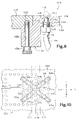
- FIG. 8 is a sectional view corresponding in viewing angle to the view of FIG. 5 of a first alternative embodiment of the interconnect assembly.
- FIG. 9 is an enlarged sectional view of the first alternative embodiment of FIG. 8 , as taken within the dashed-line region indicated by reference number 118 in FIG. 8 , together with an enlarged elevational view of certain of the device-probing ends of the probe card of FIG. 4 so as to indicate the arrangement of these ends relative to the probing areas of the assembly.
- FIG. 10 corresponds to FIG. 6 except that it shows, in solid-line view, the probing area configuration of a third alternative embodiment of the interconnect assembly especially suited for the simultaneous measurement of a pair of signal channels and further shows, in dashed-line view, different positions which the device-probing ends can occupy in relation to this probing area configuration.
- FIGS. 11 a–d are schematic plan views depicting consecutive positions of the device-probing ends of the probe card, represented in dashed-line view, on the probing areas of the exemplary interconnect assembly of FIG. 4 , represented in solid-line view, during an exemplary probe network evaluation session.
- FIG. 4 shows an exemplary interconnect assembly 48 which is constructed in accordance with the present invention and which, in accordance with a preferred method, enables accurate calibration of a multichannel probe network 21 .
- the network can include, as shown, a probe card 30 of the type having a plurality of needle-like probe tips 34 , where the lower extremities of these tips form the device-probing ends of the network and these ends are so arranged as to match the pad arrangement of a specified group of microelectronic devices 24 , such as those formed on an integrated wafer 22 .
- the assembly 48 is so configured as to enable the uniform transfer of high-frequency signals between each different end and a reference sourcing or sensing unit despite the fragility of the needle-like probe tips 34 and the closely crowded arrangement of the device-probing ends.
- the reference sourcing or sensing unit will be understood to be detachably connected to the underside of the assembly 48 by a high-frequency channel, such as a coaxial cable 49 .
- This reference unit can be provided by the same test instrument 36 which, with its different sourcing and sensing units, generates and monitors the various signals that are present in the network 21 , that is, the signals which are transferred to and from each device 24 during device measurement.
- the probe measurement network 21 includes, in addition to the probe card 30 , various sources and sensing units within the test instrument as well as the multiconductor measurement cable 38 that connects the card and instrument.
- FIG. 7 shows an enlarged elevational view of certain ones of the needle-like probe tips 34 which are included on the probe card 30 shown in FIG. 4 .
- the device-probing ends of these tips such as 50 a–b, 52 a–b and 54 a–b, are used to transfer high-frequency within the range of 100 MHZ to 2 GHz.
- the term “high-frequency” is more broadly intended, herein and in the claims, to denote any frequency within the range from 50 MHZ to 65 GHz or above.
- any device-probing end which is identified in the drawings by a reference number starting with 50 corresponds to a source channel of the probe measurement network 21 , that is, from each such end the incoming signal from a respective sourcing unit in the network 21 is directly transferred to a corresponding input pad of the device-under-test.
- any end which is identified by a reference number starting with 52 corresponds to a sense channel of the network, that is, the outgoing signal from a particular output pad of the device-under-test is directly transferred to a corresponding one of these ends for subsequent transmission to a respective sensing unit in the measurement network.
- any end which is identified by a reference number starting with 54 corresponds to a ground return line for the source and sense channels of the network, that is, during device measurement, each such end connects to a corresponding ground pad of the device-under-test so that a well-constrained ground line is established for each signal channel.
- This designation of particular ends as corresponding to either source, sense or ground return lines is conventional and is indicated herein only to clarify the operation of the exemplary interconnect assembly 48 , a portion of which is also shown in FIG. 7 in sectional view.
- the exemplary interconnect assembly 48 enables uniform transfer of high-frequency signals between the reference channel 49 and each signal-carrying end (e.g., 50 a–b and 52 a–b ). This, in turn, makes it possible to obtain accurate comparative information about the relative signal conditions in the different channels and thus, in accordance with a preferred method described hereinbelow, enables accurate calibration of the probe measurement network 21 .
- the assembly 48 includes a base assembly 56 and a movable support assembly 58 . The characteristics of the base assembly, in particular, enable signal transfer operations to be performed with substantial uniformity.
- the preferred construction of the base assembly 56 is best illustrated in FIG. 7 which, in enlarged sectional view, shows the central region of the base assembly as included within the dashed-lined area 60 identified in FIG. 5 .
- the base assembly 56 includes a base member 62 which, in the preferred embodiment shown, constitutes a plate of solid brass. A series of concentrically aligned cavities are centrally formed in this plate including a lower threaded cavity 64 within which a high-frequency coaxial adapter 68 is screwably installed.
- this adaptor is a “sparkplug” type K-connector of the type sold, for example, by Wiltron Company of Morgan Hill, Calif. under Model No. K102F.
- This adaptor enables detachable connection of different types of reference units (i.e., of sensing or sourcing type) to the base member 62 .
- Such connection can be made, as shown, through a coaxial cable 49 , the end of which includes a threaded connector 70 which is suitably dimensioned for attachment to the adapter.
- a K-connector bead 78 is mounted within the lower mounting cavity 72 .
- This bead also known in the art as a “glass” bead, is used in conventional assemblies in connection with an associated fixture in order to interconnect a K-connector of the type above described with a planar microstrip line.
- a bead of suitable type, for example, is sold by Wiltron Company under Model No. K100.
- This bead includes an inner conductor 82 that has a nominal diameter of about 12 mils.
- the first or lower end 80 of the inner conductor 82 is insertably engaged, in a conventional manner, with the tubular center conductor 84 of the K-connector 68 .
- the second or upper end 86 of the inner conductor 82 which normally extends outwardly from the bead for connection with a microstrip line, is cut short so that only a small portion of the inner conductor extends past the surrounding inner dielectric 88 of the bead, as shown.
- the inner dielectric of the bead is made of glass for low-loss transmission of high-frequency signals and the bead further includes an outer conductor or metalized rim 90 that concentrically surrounds the inner conductor 82 . This rim is soldered to the lower mounting cavity 72 so that the bead 78 is fully seated within this cavity, as shown.
- a pocket 92 is drilled into the upper end 86 of the inner conductor 82 of the bead and a length of copper wire 94 of 3 mil nominal diameter or other suitable conductor is anchored by its lower end within the pocket by a low temperature solder 95 so that the respective center axes of the wire and the inner conductor are aligned.
- An annular-shaped glass sleeve 96 of 10 mil wide outer diameter is then fitted over the wire, and the outer sides of the sleeve are epoxied to the upper mounting cavity 76 of the brass base member 62 . Within the center cavity 74 of the base member, the lower face of the glass sleeve abuts the upper end 86 of the inner conductor 82 .
- a lapping process is used to remove excess material along the upper face 104 of the base member so as to present a completely flat and smooth surface along this face.
- the upper face of the brass base member 62 and the upper end of the wire 94 are gold plated using an electroplating bath while the upper face of the glass sleeve 96 is covered by a mask.
- the plated surfaces of the wire 94 and the brass base member 62 form a first or inner planar probing area 98 and a second or outer planar probing area 100 , respectively. As shown in FIG.
- the outer probing area 100 is radially spaced apart from and completely surrounds the inner probing area 98 , and the exposed face of the glass sleeve forms an annular-shaped dielectric area or “transmission window” 102 between these two probing areas.
- the inner and outer probing areas 98 and 100 are both included on the upper face 104 of the base member 62 .
- the term “on” is intended to mean “within the outer boundaries of.” It will be seen from FIG. 7 that the inner and outer probing areas 98 and 100 and the dielectric area 102 are substantially level with each other so that there is no protruding edge along the upper face 104 of the base member that could snag and damage the delicate needle-probe tips 34 as these probe tips are being moved between different probing positions on the probing areas.
- a high-frequency transmission structure or channel 106 is formed within the base member 62 in such a manner as to be integrally connected with the respective probing areas 98 and 100 .
- the areas 98 and 100 define that section of the transmission structure which adjoins the upper surface 104 of the base member.
- This transmission structure enables high-frequency signals to travel through the base member perpendicular to the principal plane of the base member.
- the transmission structure has inner and outer boundaries where the outer boundary is formed by the upper mounting cavity 76 , the center cavity 74 and the inner surface 108 of the metalized rim 90 .
- the inner boundary of the transmission structure is formed by the respective outer surfaces of the copper wire 94 and the inner conductor 82 .
- the high-frequency transmission structure 106 is connected to the high-frequency coaxial adapter 68 at a reference junction 110 (a portion of the inner conductor 82 extends past this reference junction to mate with the tubular center conductor 84 of the coaxial adapter).
- the reference junction is suitably configured for connection to the reference sourcing or sensing unit.
- the reference unit can either be connected directly to the reference junction with its connector screwed into the lower threaded cavity 64 or, as shown in FIGS. 5 and 7 , the reference unit can be connected indirectly to the reference junction by a coaxial adapter 68 and a coaxial cable 49 .
- the advantage of using the cable is that the reference junction can, as the need arises, be flexibly connected to more than one type of reference unit.
- the reference junction 110 serves as either a presentation node or a sampling node for reference signals.
- FIG. 6 shows a plan view of the inner probing area 98 as well as that portion of the outer probing area 100 which is contained within the dashed-line area 60 indicated in FIG. 5 .
- the portions of the outer probing area that are not shown in FIG. 6 extend to the outer edges of the base member 62 ( FIG. 7 ).
- the outer probing area is considerably larger than the inner probing area and, indeed, nearly covers the entire upper side of the assembly 48 .
- the inner and outer probing areas are so arranged in relation to each other than any neighboring pair of device-probing ends of the probe assembly 30 , such as ends 50 a and 54 a , can be simultaneously placed on the inner and outer probing areas so that one end is positioned on each area.
- the compatible planar geometry of both the ends and the areas not only serves to reduce wear but also ensures that any signal exchanges between the probe assembly 30 and the interconnect assembly 48 occur uniformly through the extreme ends of the probe assembly rather than through signal exchange sites on the probe assembly that are randomly located further up along the probe tips.
- this transmission line assumes the form of a coaxial-type channel having inner and outer conductive boundaries, as previously noted, where the diameter of the inner and outer boundaries changes in a stepwise manner along the axis of the channel so as to reduce transition discontinuities.
- transmission line as used herein and in the claims is intended to denote any signal-guiding structure that includes spaced-apart boundaries, where the boundaries are capable of supporting a high-frequency field so as to enable the propagation of a high-frequency signal along the boundaries.
- boundaries can comprise, for example, reflection surfaces between which, at any section of the line, there is a predetermined spacing to ensure signal stability.
- the preferred embodiment of the transmission structure 72 has boundaries which are formed by certain portions of the metallic surfaces of the brass base member 62 , the K-connector bead 78 and the copper wire 94 , for certain applications it may be preferable to construct the transmission structure without any metallic materials.
- the term “conductive,” as used herein and in the claims, is intended to refer generally to the ability of a certain element to conduct a signal without limitation as to whether or not, for example, the element is a metal.
- the configuration of the transmission structure 106 is such that for each different position that the ends 50 a and 54 a can occupy when they are placed on the corresponding areas 98 and 100 , the transmission line which the structure provides between these ends and the reference junction 110 has a substantially constant high-frequency transmission characteristic.
- the transmission structure is so configured that a signal traveling along the structure propagates in a direction perpendicular to the plane of the probing areas rather than in a direction parallel to that plane.
- the size of the inner probing area 98 is not determined by the length of the transmission structure and hence can be reduced, as shown, to a dimension approximately corresponding to that of each device-probing end.
- FIGS. 11 a – 11 d which indicate, with directional arrows, how the exemplary interconnect assemmbly 48 is shifted in mutually perpendicular directions during a typical network evaluation session in order to consecutively position different ends of the probe array on the inner probing area 98 , including the corner ends 50 c – 50 f.
- FIGS. 11 a – 11 d indicate, with directional arrows, how the exemplary interconnect assemmbly 48 is shifted in mutually perpendicular directions during a typical network evaluation session in order to consecutively position different ends of the probe array on the inner probing area 98 , including the corner ends 50 c – 50 f.
- the device-probing ends of the network are represented in dashed-line view and the number of ends per side is considerably reduced from their actual number for ease of illustration.
- FIG. 11 a it will be recognized that when the signal-carrying end 50 c is positioned on the inner probing area 98 , the corresponding ground return end 54 c is positioned on the outer probing area 100 in a position lying to the “east” of the inner probing area.
- FIG. 11 b when the signal-carrying end 50 d is positioned on the inner probing area because of a shift by the exemplary assembly 48 in the direction indicated in FIG.
- the corresponding ground return end 54 d is positioned on the outer probing area in a position that now lies to the “north” of the inner probing area.
- the respective ground return ends it is also possible for the respective ground return ends to occupy positions on the outer probing area that lie to the west or south of the inner probing area.
- the corresponding transmission path provided by the transmission structure 106 is substantially the same for each position. Referring to FIGS. 6 and 7 together, it will be recognized that as long as the subject signal-carrying end remains in its position on the inner probing area 98 , the geometry, and hence circuit characteristic, of the outer probing area 100 will appear substantially identical to the corresponding ground return end for any angular position which that end can then occupy.
- the exemplary transmission structure 72 provides an omnidirectional transmission line which, in relation to any pair of corresponding ends, presents a substantially uniform transmission characteristic for any angle which those ends can assume while remaining on their corresponding areas.
- the exemplary transmission structure 106 therein shown not only provides a stable transmission line between the ends of the probing network and the reference junction 110 for different positions of the ends on the corresponding areas 98 and 100 , but also is so configured that high-frequency signals that are present in the environment but that are not the subject of evaluation will, as a general matter, be prevented from entering this transmission line.
- the incoming signal that is the subject of evaluation in FIG. 7 that is, the signal which is contained in the field supported by ends 50 a and 54 a, will have little difficulty passing through the energy “window” that is provided by the dielectric area 102 between the inner probing area 98 and the outer probing area 100 .
- the incoming signal that is contained in the field supported by ends 50 b and 54 a which signal is not of interest, will be reflected the moment it reaches the plane of the outer probing area 100 in a direction away from the transmission line.
- the outer surfaces of the base member 62 form an electromagnetic shield in relation to the transmission line that substantially prevents radiation from entering the line from any source adjacent the substrate's upper face 70 that is other than the device-probing end under evaluation.
- the base assembly 56 facilitates uniformity of signal transfer between the device-probing ends of the network and the reference junction 110 .
- the signals which pass between the ends and the reference junction are substantially unaffected by the type of variation in probing position that is likely to occur as the inner probing area 98 is shifted from end-to-end.
- the base assembly 56 rejects high-frequency signals, except from the subject channel, so that these signals cannot enter the evaluation path and distort the signal of interest. Accordingly, at least two distinct aspects about the base assembly 56 facilitate uniformity of signal transfer, namely its substantial immunity to normal probing position variation and its substantial immunity to spurious signals.
- the interconnect assembly 48 is shown.
- the base member 116 constitutes a substrate which is only about 5 to 25 mils thick with a nominal thickness of about 10 mils.
- This substrate is preferably made of glass or other hard dielectric material in order to reduce the flow of leakage currents within the substrate at higher frequencies.
- FIG. 9 which is an enlarged view of the dashed-line area 118 shown in FIG.
- a first or inner planar probing area 120 and a second or outer planer probing area 122 are formed by a metalization process on the upper face 124 of the base member so that these areas are in mutually coplanar relationship with each other.
- the first and second probing areas 120 and 122 define the upper end of a transmission structure 125 that enables high-frequency signals to travel through the base member perpendicular to the principal plane of such base member.
- the inner and outer boundaries of the transmission structure are formed by a first or inner conductive via 126 and a second or outer conductive via 128 , respectively, where the outer conductive via is generally annular in shape.
- Each via 126 or 128 is embedded within the substrate and extends directly beneath the corresponding probing area 120 or 122 .
- the first alternative embodiment 114 of the interconnect assembly like the exemplary interconnect assembly 48 , includes a reference junction 130 .
- this reference junction is defined by that section of the high frequency transmission structure 125 which is contiguous with the lower surface of the substrate 116 .
- the movable support assembly 131 of the first alternative interconnect assembly 114 includes a horizontal portion 132 .
- a concentrically aligned series of cavities 134 , 136 and 138 are formed in this horizontal portion, and a high-frequency “sparkplug” type connector 140 is screwably installed into the lowest cavity 134 .
- a protruding portion of an inner dielectric 142 of this connector is received by the center cavity 136 , and an exposed center conductor 144 of the connector passes through the upper cavity 138 for electrical connection with the inner via 126 .
- the outer conductive shell 146 of the connector 140 makes electrical connection with the outer via 128 through the conductive body of the movable support assembly 131 .
- Solder, conductive epoxy or other electrically conductive joining material is used to permanently bond the center conductor 144 to the inner via and the conductive body of the movable support assembly 131 to the outer via. These connections ensure continuity in the ground return path for any ground return end positioned on the outer probing area 122 and also provide a well-isolated controlled impedance path for all signals transmitted between the reference junction 130 and the reference channel 49 .
- the high-frequency connector 140 of the first alternative interconnect assembly 114 can be removed, and the connector head of a reference unit can be connected directly to the reference junction 130 .
- the outer boundaries of the inner probing area 120 and the outer probing area 122 are defined by an inner well 148 and an outer well 150 , respectively, that are formed on the upper face 124 of the substrate 116 .
- a high-definition masking process and a suitable etching agent, such as hydrofluoric acid, are used to form these wells.
- the wells are separated from each other by a narrow annular ridge 152 of substrate material.
- inner and outer sloping wall channels 154 and 156 are formed using a laser. These channels define the boundaries of the inner and outer vias 126 and 128 .
- the translucent property of the glass substrate permits the laser beam to be accurately focused directly opposite and on-center with the well 148 that was previously etched for the inner probing area.
- the inner and outer wells 148 and 150 and the corresponding sloping wall channels 154 and 156 are then filled with nickel or some other suitably hard metal (such as tungsten, iridium or rhodium) in such a manner that the metal in the wells is able to fuse with the metal in the channels.
- the sloping-wall shape of each channel facilitates this fusing process by making it easier for the metal to flow into and completely occupy each channel.
- An alternative approach is to omit the step of forming the wells 148 and 150 and to simply deposit extremely thin layers of conductive material on the substrate 116 to form the probing areas 120 and 122 .
- this alternative approach there is a significant risk that the ends of the tips 34 will punch through the thin probing areas if an excessive amount of contact force is applied between these ends and the areas.
- the upper surfaces of the inner and outer probing areas 120 and 122 are then lapped until the resulting overall surface is completely flat and smooth. As with the exemplary interconnect assembly 48 , this step ensures that there are no protruding edges left on the upper face of the assembly 114 which could snag and damage the delicate needle-like tips during repositioning of the assembly.
- the maximum edge-to-edge dimension 157 of the inner probing area 120 is nominally 4 mils while the radially-extending gap 158 between the inner and outer probing areas 120 and 122 is nominally 1 ⁇ 2 mil across.
- first alternative interconnect assembly 114 it will be recognized that the basic components of this assembly correspond to those of the exemplary interconnect assembly 48 , insofar as both assemblies include a base member 62 or 116 , first and second planar probing areas 98 and 100 or 120 and 122 on the base member, a transmission structure 106 or 125 extending perpendicular to the principal plane of the base member and a reference junction 110 or 130 that serves as a connection site for the reference unit.
- the assembly 114 is able to uniformly transfer signals despite variation in the position of the device-probing ends 34 on the probing areas and, furthermore, is able to reject spurious signals that originate outside of the channel under evaluation.
- both the exemplary interconnect assembly 48 and the first alternative interconnect assembly 114 include two probing areas on their respective upper faces consisting of the inner probing area 98 or 120 and the outer probing area 100 or 122 .
- This configuration is suitable for the closely crowded needle-like tips 34 ( FIG. 4 ) which are commonly used to test microelectronic devices, particularly since the signal field of any one channel in this type of network is supported between a corresponding signal tip and a nearby ground return tip.
- FIG. 10 shows a second alternative embodiment 160 of the assembly which includes three probing areas for use in evaluating network conditions such as cross-talk.
- This embodiment includes a base assembly comprising a substrate 162 on the upper face of which is a first inner probing area 164 , a second inner probing area 166 and a third or outer probing area 168 . If the substrate 162 were to be viewed in section along the reference line 170 , the resulting figure would correspond closely to FIG. 9 except that there would be a pair of inner vias in balanced arrangement within the outer via 128 instead of only one inner via 126 .
- the device-probing ends are represented in dashed-line view.
- the entire probing array is depicted in order to show how the square-like probing array is preferably oriented in relation to the three probing areas during evaluation of the probing network.
- the number of ends per side of the array has been reduced from their actual number for convenience and clarity.
- the two signal-carrying ends 50 a and 50 b correspond to the two channels of the network that are the subject of interest and that the corresponding ground return end is 54 a. It will be recognized that when these ends are in the center probing position illustrated, that is, when these ends are aligned with reference line 170 , then the ends are mispositioned since end 50 a, corresponding to a signal-carrying channel, properly belongs on one of the inner or signal probing areas 164 or 166 , while end 54 a, corresponding to a ground return line, properly belongs on the outer or ground probing area 168 . It is possible, however, to shift the substrate 162 so as to simultaneously position these three ends on corresponding ones of the areas.
- the substrate can be shifted so that the first signal-carrying end 50 a occupies a position on the first inner probing area 164 , the second signal-carrying end 50 b simultaneously occupies a position on the second inner probing area 166 and the ground return end 54 a simultaneously occupies a position on the third or outer probing area 168 .
- the substrate can be shifted in the ⁇ X and ⁇ Y directions indicated in order to reposition these ends to the illustrated probing position that is in alignment with reference line 172 .
- the substrate can be shifted in the +X and ⁇ Y directions indicated in order to reposition these ends to the illustrated probing position that is in alignment with reference line 174 .
- FIG. 10 also illustrates how the probing area configuration provided by the second alternative embodiment 160 accommodates the evaluation of cross-talk between two network channels even when the corresponding ends of the network are spaced widely apart, as is the case with ends 50 g and 50 h.
- each interconnect assembly provides a means through which different types of reference units can be conveniently connected to the corresponding reference junction 110 or 130 .
- various other types of connections to each reference junction are also possible.
- a pair of coaxial adapters instead of only one adapter could be connected to the junction.
- This last type of connection is the type preferably used, for example, where the interconnect assembly includes a pair of inner probing areas 164 and 166 , as shown in FIG. 10 .
- the second alternative embodiment 160 shown in FIG. 10 is configured so as to include two inner vias, thus providing sufficient attachment sites for the connection of two adapters. Such connection permits differential measurements to be made between two different signal channels of the probing network.
- any coaxial adapter that is provided on the base member would be included on the upper side of such base member (i.e., in a position that would not interfere with the placement of the device-probing ends).
- a two-section transmission line may be used, where one section extends between the reference junction and a point opposite the adapter and the second section, starting from that point, extends through the substrate to the adapter.
- Still another variation is to connect a first circuit element to the reference junction on the basis of the characteristics of a second circuit element that is connected directly between the inner and outer probing areas 98 and 100 so that a signal entering the transmission structure 106 will, in effect, see a different circuit depending on whether it enters that structure from the upper or lower end.
- the types of elements that are suitable for connection directly between the inner and outer probing areas include chip resistors, capacitors and inductors.
- Yet another variation is to utilize a connected pair of interconnect assemblies 48 and to support this pair of assemblies so that the spacing between the corresponding pair of inner probing areas 98 is adjustable so as to enable probing of the inner probing area of one of the assemblies by a selected one of the “stimulus” probe ends (e.g., 50 b ) while concurrently enabling probing of the inner probing area of the other assembly by a designated one of the “response” probe ends (e.g., 52 b ) regardless of the spacing that exists between these ends.
- the outer probing area 100 surrounding each inner probing area is reduced in size (e.g., to a nominal radius of about 20 mils) so that the respective inner probing areas of the corresponding assemblies can be moved adjacent to each other when measurements are to be taken across nearby probe ends.
- the high-frequency adapters 68 of the two assemblies are normally connected together by a short length of flexible coaxial line, although other types of circuit elements can be used as well.
- the relative positions of the two assemblies may be adjusted by providing a first mechanism for adjusting the linear separation between the two assemblies, a second mechanism for rotating both assemblies in unison, and a third mechanism for effecting X-Y-Z directional movements of the wafer stage that carries both assemblies.
- the exemplary interconnect assembly 48 hereinabove described is combined with the probe station containing the measurement network 21 so as to form an integrated self-evaluating probing system 176 .
- the exemplary interconnect assembly can either be mounted directly on the wafer-supporting chuck 178 , as shown, or can be mounted separately off to one side of the chuck.
- this mounting method also allows the probe tips to be shifted between their various device-measuring positions and their various channel-evaluating positions using the same motorized X-Y-Z positioning table 182 included in this system for positioning the chuck.
- the interconnect assembly 48 is mounted in adjoining relationship to the wafer-supporting chuck 178 , is mounted separately off to one side of the chuck, or is transported to the chuck as the need arises, it is advantageous when evaluating the probing network 21 to locate the interconnect assembly in the wafer-probing station, rather than locating it in a separate evaluation station, in order to permit in situ evaluation of the network.
- the exemplary interconnect assembly 48 was so constructed that it could not operate properly unless the signals entering through the network were first routed through an intermediate processing unit, then to use this assembly, it would be necessary to change the connections of the original measurement network in order to connect the unit between the network and the assembly.
- the probe card 30 might be disconnected from the original measurement cable 38 and removed to a separate evaluation station for connection to the processing unit.
- evaluation of the probe card portion of the network would be performed separately from evaluation of the cable and instrument portions of the network, the resulting procedure would be inherently slower and less accurate than in situ evaluation where the entire network is evaluated at the same time.
- the exemplary interconnect assembly 48 does not require a processing unit anywhere between its probing areas 98 and 100 and the probing network 21 in order for it to function properly. If, for example, the source channels of the probing network 21 are the subject of evaluation, the only connection needed to the interconnect assembly is the connection of a reference sensing unit to the reference junction 110 of the assembly. Typically, the original test instrument 36 will include at least one sensing unit that is not being used for device measurement, which can then be connected to the reference junction through the reference cable or channel 49 . On the other hand, if the sense channels of the probing network 21 are the subject of evaluation, then the only connection needed to the assembly is the connection of a sourcing unit to the same reference junction. Typically, the original test instrument will further include an unused sourcing unit which can be connected to the reference junction merely by switching the reference cable 49 to the corresponding port on the instrument, as through a switching device.
- the same piece of equipment 36 that is included in the system 176 to process the signals needed for device measurement can also be used, in conjunction with the exemplary interconnect assembly 48 , to process the signals needed for evaluating the system's own probing network, and there is no need, however the assembly is connected, to divide the network 21 into separate parts in order to use the assembly to evaluate the network.
- the interconnect assembly 48 is bidirectionally operable and hence can be used to evaluate each channel of the original probing network 21 regardless of whether the channel under evaluation is of source or sense type.
- end 54 a provides the ground return path in relation to the signal-carrying end 50 a. More generally, however, the ground return path corresponding to end 50 a may be provided by an end that is not immediately adjacent to end 50 a, such as end 54 b. In accordance with this more general situation, during device measurement, if end 50 a were to be positioned on an input pad of a device under test, then end 54 b would be positioned on a ground pad of the same device, so that a continuous ground path would be formed as a result of connection between end 54 b and the ground pad.
- This continuous ground path would have an effect on the characteristics of the circuit that is formed through ends 50 a and 54 b.
- This same continuity of ground path is provided, however, by the outer probing area 100 , since this area is connected to the ground shield of the reference cable 49 through the outer shell of the threaded connector 70 , the outer conductive shell of the coaxial adapter 68 , and the conductive body of the brass base member 62 .
- the outer probing area 100 appears the same as the ground pad of a device under measurement and thus the channel conditions present during device measurement are substantially duplicated during network evaluation.
- any end that is out of contact with the inner probing area 98 will automatically be positioned in contact with the outer probing area 100 .
- FIGS. 11 a – 11 d for example, even if the end under evaluation is at one of the four extreme corners of the probe array, as is the case with ends 50 c, d, e and f, if this end is positioned on the inner probing area 98 , then all of the other ends, which include the ground return ends 54 c, d, e and f, are automatically positioned simultaneously on the outer probing area 100 .
- the inner and outer probing areas 120 and 122 of the first alternative embodiment 114 are so arranged as to produce the same result.
- the second alternative embodiment 160 shown in FIG. 10 if two signal-carrying ends, such as 50 a and 50 b, are simultaneously positioned so that each is on a corresponding one of the inner probing areas 164 or 166 , then the other ones of the ends, such as the ground return end 54 a, are automatically positioned simultaneously on the outer probing area 168 .
- the outer probing area 100 , 122 or 168 will present the same characteristics to that end as would have been presented by the ground pad of a device during device measurement. It will be noted, on the other hand, that if any end not under evaluation corresponds to a source channel, such as end 50 b in FIG. 7 , the outer probing area will reflect the signal carried by that end away from the transmission structure 106 or 125 , thereby preventing that signal from entering the evaluation channel and distorting the signal of interest.
- the respective probing areas of the interconnect assembly 48 are continuously available for probing by the probing tips 34 free of any requirement for removal of the wafer from the chuck. This, in turn, facilitates rapid back-and-forth shifting of the probe tips 34 between various device-testing positions on the wafer and various channel-evaluating positions on the interconnect assembly.
- a programmable microprocessor 184 to control the motorized X-Y-Z positioning table 182 .
- This microprocessor is programmed to deliver, in quick succession, a series of control commands to the positioning table so that predetermined ones of the device-probing ends are positioned by the table, likewise in quick succession, on the inner probing area 98 during network evaluation.
- the reference junction 110 is connected to a reference sensing unit, and the microprocessor 183 , in response to a user-generated signal, commands the positioning table to shift so as to move the inner probing area 98 to its starting position (e.g., in contact with end 50 c ) as shown in FIG. 11 a.
- the microprocessor commands the positioning table 182 to move in specified increments along the +Y direction indicated so that, ultimately, each end along this direction that corresponds to a source channel, such as ends 50 c and 50 d, is successively positioned on the inner probing area 98 . Referring to FIG.
- the microprocessor next commands the positioning table to move by specified increments in the ⁇ X direction indicated so that each end along this direction that corresponds to a source channel, including ends 50 d and 50 e, is successively brought into contact with the inner probing area 98 .
- the same procedure is repeated in the ⁇ Y direction and the +X direction, thus successively positioning each of the ends in the probing array that corresponds to a source channel into contact with the inner probing area.
- the microprocessor 184 begins the sequence by commanding the positioning table 182 to move by specified increments in the +Y direction indicated, so that each end along that direction that corresponds to a sense channel is successively positioned on the inner probing area, including ends 52 c and 52 d. This time, ends 50 c and 50 d, which correspond to source channels, are passed over. The remainder of the sequence proceeds in similar manner with respect to the other directions.
- the microprocessor 184 can be programmed so that it will instruct the positioning table 182 to successively shift the inner probing area 98 into contact with each end that generally corresponds to a signal channel. Depending, then, on whether the end specifically corresponds to a source channel or to a sense channel, a switching device that is operated by a control line from the microprocessor will automatically connect the reference junction 110 to either a sensing unit or a sourcing unit on the test instrument 36 .
- a primary advantage to using the same probing area 98 for evaluating each signal channel is that if there are any differences detected between the signals in the different channels, these differences can be attributed directly to the signal channels themselves without further investigation required into the extent to which these differences might be based on differences in evaluation path. It may also be noted that while the primary anticipated use of the exemplary interconnect assembly 48 is for the comparative evaluation of probe measurement channels, the assembly can also be used for those situations where quick verification is needed of the quality of signal at a particular end while device measurement is in progress.
- the inner probing area 98 , the dielectric area 102 and the outer probing area 100 are substantially level with each other so that there is no protruding shoulder along the upper face of the assembly which could snag and damage the tips.
- the movable support assembly 58 of the interconnect assembly is provided with a vertical adjustment knob 186 that enables adjustable positioning of the height of the base member 62 relative to the wafer-supporting chuck 178 so that the respective probing areas 98 and 100 are arranged in adjustable parallel relationship to the imaginary plane defined by the upper surface of the chuck.
- the movable support assembly 58 defines a threadless hole 188 through which the shank of the knob bolt is inserted in order to engage the block while the end threads of this shank engage an internally threaded bore 190 on the underside of the chuck 178 .
- the interconnect assembly 48 can be raised or lowered relative to the chuck.
- the exemplary interconnect assembly 48 can be used for evaluating the signal conditions in a probe measurement network 21 of the type suitable for probing of planar microelectronic devices. More specifically, the interconnect assembly can be used not just to evaluate the network but also to calibrate the network in accordance with a preferred method that will now be described.
- the object of this calibration can include normalizing the signal conditions in the network in relation to the device-probing ends so that when measurements of a device are made through these ends, any channel-to-channel differences which are then detected are attributable solely to the characteristics of the device.
- At least some of the device-probing ends that correspond to source channels in the network 21 provide different incoming signals to the corresponding input pads of whichever device 24 is under test because each incoming signal is normally transmitted from the port of a different data generating or other sourcing unit within the test instrument 36 and travels along a different transmission path (e.g., through a different conductor in the measurement channel 38 and a different conductor in the probe card 30 ) to reach the corresponding device-probing end. Accordingly, unless the differences between these incoming signals are somehow compensated for, what is measured at the respective output pads of the device reflects not only the characteristics of the device itself but also these channel-to-channel differences in the incoming signals from the measurement network.
- a reference sensing unit on the test instrument 36 such as a spare logic analyzing unit, is connected to the interconnect assembly 48 through the reference cable or channel 49 .
- the preferred calibration method includes positioning end 50 a into contact with the inner probing area 98 and transmitting an incoming signal through the corresponding source channel. This signal enters the transmission structure 106 and, from there, is transmitted through the reference junction 110 and along the reference cable 49 to the logic analyzing unit of the test instrument. This step is then repeated with respect to end 50 b.
- the exemplary assembly 48 is preferably shifted by the automatic positioning mechanism described above so as to position the end 50 b into contact with the inner probing area 98 and a second incoming signal is then transmitted through the corresponding source channel.
- This second signal like the first signal from end 50 a, enters the transmission structure 106 and follows the same evaluation path through the reference junction 110 to the same logic analyzing unit.
- the transmission structure 106 provides a transmission line of substantially constant high-frequency transmission characteristic between each end coming into contact with the inner probing area 98 and the reference junction 110 . Accordingly, the characteristics of the entire evaluation path between each end and the logic analyzing unit are substantially the same for each signal. This means, in turn, that in the example just given, after the first and second incoming signals are measured at the logic analyzing unit, if a comparison of the resulting measured values indicates that there is a difference between the two signals, then this same difference correspondingly exists in reference to the device-probing ends 50 a and 50 b.
- either a computational approach can be used (under which, for example, a suitable numerical offset is added to the readings that are taken through each different source channel) or the probing network 21 itself can be adjusted or altered (this could include, for example, automatically tuning each data generating unit of the test instrument 36 until the incoming signals are substantially identical in reference to the reference sensing unit).
- the exemplary calibration procedure just described can be used to correct for the effects of various types of signal differences, including differences in phase delay, differences in signal level, differences in noise level and so on.
- the type of parameter that is under evaluation will determine the type of sensing unit required. If, for example, the object is to normalize noise levels in the different channels, a noise meter unit or other like sensing unit should be used instead of a logic analyzing unit.
- the exemplary interconnect assembly 48 is bidirectionally operable, it is also possible to use the assembly for accurately calibrating the sense channels of the probing network.
- Calibration of the sense channels is normally necessary because typically at least some of the sense channels provide conditions for the signals during transmission and measurement that are different than those provided in other ones of the channels. That is, each outgoing signal from a device-under-test, upon entering the corresponding device-probing end of the network, travels along a different transmission path (corresponding to a different conductor in the probe card 30 and a different conductor in the measurement channel 38 ) and is measured by a different sensing unit in the test instrument 36 , which unit has its own individual response characteristic.
- the object of calibration with respect to the source channels of the network is to compensate for these channel-to-channel transmission and measurement differences so that if identical outgoing signals are presented, for example, to the sense channels by the device-under-test, then this condition is directly and accurately detected by the test instrument.
- a reference sourcing unit on the test instrument 36 such as a spare data generating unit, is connected to the interconnect assembly 48 through the reference cable or channel 49 .
- the preferred calibration method includes positioning end 52 a into contact with the inner probing area 98 and transmitting a reference signal from the reference sourcing unit. This outgoing signal is transmitted through the reference junction 110 and then through the source channel corresponding to end 52 a until it reaches the corresponding sensing or logic analyzing unit of the test instrument, where it is measured.
- end 52 b is positioned into contact with the inner probing area 98 by the automated positioning mechanism above described.
- a second reference signal identical to the first is transmitted from the reference sourcing unit and, like the first signal, passes through the reference junction and then through the sense channel corresponding to end 52 b until it reaches the respective sensing or logic analyzing unit that corresponds to this second channel, where it is measured.
- the outgoing signal that is presented to each end 52 a and 52 b will be substantially identical. Accordingly, if the signal readings of the two sensing units that correspond to ends 52 a and 52 b are compared and any difference is found to exist between these readings, then this indicates that there are different signal conditions in the two sense channels that correspond to ends 52 a and 52 b.
- the interconnect assembly 48 instead of being mounted to a corner of the probe station chuck, could take the form of a wafer-like device that could be readily transported from chuck-to-chuck and which could be held, on each chuck, by the same vacuum lock used for holding wafers.
- the interconnect assembly instead of being mounted to a corner of the probe station chuck, could take the form of a wafer-like device that could be readily transported from chuck-to-chuck and which could be held, on each chuck, by the same vacuum lock used for holding wafers.
- different types of reference sourcing and sensing units can be connected in different ways to the reference junction of the interconnect assembly depending on what types of conditions are being evaluated. In addition to these and other variations described above, further variations will be evident to those of ordinary skill in the art from the foregoing description.
Landscapes
- General Physics & Mathematics (AREA)
- Physics & Mathematics (AREA)
- Engineering & Computer Science (AREA)
- Chemical & Material Sciences (AREA)
- Nanotechnology (AREA)
- Crystallography & Structural Chemistry (AREA)
- Molecular Biology (AREA)
- General Health & Medical Sciences (AREA)
- Life Sciences & Earth Sciences (AREA)
- Health & Medical Sciences (AREA)
- Computer Hardware Design (AREA)
- Microelectronics & Electronic Packaging (AREA)
- General Engineering & Computer Science (AREA)
- Testing Or Measuring Of Semiconductors Or The Like (AREA)
- Measuring Leads Or Probes (AREA)
- Testing Of Individual Semiconductor Devices (AREA)
- Tests Of Electronic Circuits (AREA)
Abstract
Description
Claims (13)
Priority Applications (2)
| Application Number | Priority Date | Filing Date | Title |
|---|---|---|---|
| US11/298,799 US7164279B2 (en) | 1995-04-14 | 2005-12-09 | System for evaluating probing networks |
| US11/652,788 US7321233B2 (en) | 1995-04-14 | 2007-01-11 | System for evaluating probing networks |
Applications Claiming Priority (9)
| Application Number | Priority Date | Filing Date | Title |
|---|---|---|---|
| US08/422,439 US5561377A (en) | 1995-04-14 | 1995-04-14 | System for evaluating probing networks |
| US08/669,097 US5659255A (en) | 1995-04-14 | 1996-06-26 | Method of evaluating signal conditions in a probe measurement network having a plurality of separate measurement channels |
| US08/866,165 US5869975A (en) | 1995-04-14 | 1997-05-30 | System for evaluating probing networks that have multiple probing ends |
| US09/175,062 US5973505A (en) | 1995-04-14 | 1998-10-19 | System for evaluating probing networks |
| US09/359,989 US6130544A (en) | 1995-04-14 | 1999-07-22 | System for evaluating probing networks |
| US09/611,806 US6608496B1 (en) | 1995-04-14 | 2000-07-07 | Reference transmission line junction for probing device |
| US10/459,259 US6803779B2 (en) | 1995-04-14 | 2003-06-11 | Interconnect assembly for use in evaluating probing networks |
| US10/951,917 US6987398B2 (en) | 1995-04-14 | 2004-09-28 | System for evaluating probing networks |
| US11/298,799 US7164279B2 (en) | 1995-04-14 | 2005-12-09 | System for evaluating probing networks |
Related Parent Applications (1)
| Application Number | Title | Priority Date | Filing Date |
|---|---|---|---|
| US10/951,917 Continuation US6987398B2 (en) | 1995-04-14 | 2004-09-28 | System for evaluating probing networks |
Related Child Applications (1)
| Application Number | Title | Priority Date | Filing Date |
|---|---|---|---|
| US11/652,788 Continuation US7321233B2 (en) | 1995-04-14 | 2007-01-11 | System for evaluating probing networks |
Publications (2)
| Publication Number | Publication Date |
|---|---|
| US20060103403A1 US20060103403A1 (en) | 2006-05-18 |
| US7164279B2 true US7164279B2 (en) | 2007-01-16 |
Family
ID=23674892
Family Applications (10)
| Application Number | Title | Priority Date | Filing Date |
|---|---|---|---|
| US08/422,439 Expired - Lifetime US5561377A (en) | 1995-04-14 | 1995-04-14 | System for evaluating probing networks |
| US08/669,097 Expired - Lifetime US5659255A (en) | 1992-06-11 | 1996-06-26 | Method of evaluating signal conditions in a probe measurement network having a plurality of separate measurement channels |
| US08/866,165 Expired - Fee Related US5869975A (en) | 1995-04-14 | 1997-05-30 | System for evaluating probing networks that have multiple probing ends |
| US09/175,062 Expired - Fee Related US5973505A (en) | 1995-04-14 | 1998-10-19 | System for evaluating probing networks |
| US09/359,989 Expired - Fee Related US6130544A (en) | 1995-04-14 | 1999-07-22 | System for evaluating probing networks |
| US09/611,806 Expired - Fee Related US6608496B1 (en) | 1995-04-14 | 2000-07-07 | Reference transmission line junction for probing device |
| US10/459,259 Expired - Fee Related US6803779B2 (en) | 1995-04-14 | 2003-06-11 | Interconnect assembly for use in evaluating probing networks |
| US10/951,917 Expired - Fee Related US6987398B2 (en) | 1995-04-14 | 2004-09-28 | System for evaluating probing networks |
| US11/298,799 Expired - Fee Related US7164279B2 (en) | 1995-04-14 | 2005-12-09 | System for evaluating probing networks |
| US11/652,788 Expired - Fee Related US7321233B2 (en) | 1995-04-14 | 2007-01-11 | System for evaluating probing networks |
Family Applications Before (8)
| Application Number | Title | Priority Date | Filing Date |
|---|---|---|---|
| US08/422,439 Expired - Lifetime US5561377A (en) | 1995-04-14 | 1995-04-14 | System for evaluating probing networks |
| US08/669,097 Expired - Lifetime US5659255A (en) | 1992-06-11 | 1996-06-26 | Method of evaluating signal conditions in a probe measurement network having a plurality of separate measurement channels |
| US08/866,165 Expired - Fee Related US5869975A (en) | 1995-04-14 | 1997-05-30 | System for evaluating probing networks that have multiple probing ends |
| US09/175,062 Expired - Fee Related US5973505A (en) | 1995-04-14 | 1998-10-19 | System for evaluating probing networks |
| US09/359,989 Expired - Fee Related US6130544A (en) | 1995-04-14 | 1999-07-22 | System for evaluating probing networks |
| US09/611,806 Expired - Fee Related US6608496B1 (en) | 1995-04-14 | 2000-07-07 | Reference transmission line junction for probing device |
| US10/459,259 Expired - Fee Related US6803779B2 (en) | 1995-04-14 | 2003-06-11 | Interconnect assembly for use in evaluating probing networks |
| US10/951,917 Expired - Fee Related US6987398B2 (en) | 1995-04-14 | 2004-09-28 | System for evaluating probing networks |
Family Applications After (1)
| Application Number | Title | Priority Date | Filing Date |
|---|---|---|---|
| US11/652,788 Expired - Fee Related US7321233B2 (en) | 1995-04-14 | 2007-01-11 | System for evaluating probing networks |
Country Status (3)
| Country | Link |
|---|---|
| US (10) | US5561377A (en) |
| JP (1) | JP4024324B2 (en) |
| DE (1) | DE19614506B4 (en) |
Cited By (4)
| Publication number | Priority date | Publication date | Assignee | Title |
|---|---|---|---|---|
| US20100109695A1 (en) * | 2000-09-05 | 2010-05-06 | Cascade Microtech, Inc. | Chuck for holding a device under test |
| US8319503B2 (en) | 2008-11-24 | 2012-11-27 | Cascade Microtech, Inc. | Test apparatus for measuring a characteristic of a device under test |
| US9905954B2 (en) * | 2016-02-24 | 2018-02-27 | Delta Networks, Inc. | Power transmission device and manufacturing method thereof |
| US11131699B2 (en) * | 2017-09-07 | 2021-09-28 | National Institute Of Advanced Science And Technology | Method for determining probe angle, high-frequency test system, program and storage medium |
Families Citing this family (64)
| Publication number | Priority date | Publication date | Assignee | Title |
|---|---|---|---|---|
| US5345170A (en) | 1992-06-11 | 1994-09-06 | Cascade Microtech, Inc. | Wafer probe station having integrated guarding, Kelvin connection and shielding systems |
| US6380751B2 (en) | 1992-06-11 | 2002-04-30 | Cascade Microtech, Inc. | Wafer probe station having environment control enclosure |
| US5561377A (en) * | 1995-04-14 | 1996-10-01 | Cascade Microtech, Inc. | System for evaluating probing networks |
| KR0149325B1 (en) * | 1995-05-17 | 1998-12-01 | 김광호 | How to adjust the probe |
| KR100187727B1 (en) * | 1996-02-29 | 1999-06-01 | 윤종용 | Contact check device to check processor contact failure and integrated circuit device inspection system |
| US5831443A (en) * | 1996-06-05 | 1998-11-03 | Applied Precision, Inc. | Probe card array check plate with transition zones |
| US6586954B2 (en) * | 1998-02-10 | 2003-07-01 | Celadon Systems, Inc. | Probe tile for probing semiconductor wafer |
| US6201402B1 (en) * | 1997-04-08 | 2001-03-13 | Celadon Systems, Inc. | Probe tile and platform for large area wafer probing |
| US6127831A (en) * | 1997-04-21 | 2000-10-03 | Motorola, Inc. | Method of testing a semiconductor device by automatically measuring probe tip parameters |
| US6002263A (en) | 1997-06-06 | 1999-12-14 | Cascade Microtech, Inc. | Probe station having inner and outer shielding |
| US6052807A (en) * | 1997-12-23 | 2000-04-18 | Hewlett-Packard Company | Multiple probe test equipment with channel identification |
| US6131175A (en) * | 1998-01-29 | 2000-10-10 | Hewlett Packard Co. | Automatic selection of a special mode of operation in multi-channel test equipment |
| CH694831A9 (en) * | 1998-04-24 | 2005-10-14 | Int Rectifier Corp | Device for Testing singulated semiconductor chips. |
| US6208375B1 (en) * | 1999-05-21 | 2001-03-27 | Elite Engineering Corporation | Test probe positioning method and system for micro-sized devices |
| US6445202B1 (en) | 1999-06-30 | 2002-09-03 | Cascade Microtech, Inc. | Probe station thermal chuck with shielding for capacitive current |
| US6437587B1 (en) * | 1999-11-04 | 2002-08-20 | Agilent Technologies, Inc. | ICT test fixture for fine pitch testing |
| US8214254B1 (en) | 2000-01-07 | 2012-07-03 | Home Producers Network, Llc | Method and system for compiling a consumer-based electronic database, searchable according to individual internet user-defined micro-demographics (II) |
| US7720707B1 (en) | 2000-01-07 | 2010-05-18 | Home Producers Network, Llc | Method and system for compiling a consumer-based electronic database, searchable according to individual internet user-defined micro-demographics |
| US6914423B2 (en) | 2000-09-05 | 2005-07-05 | Cascade Microtech, Inc. | Probe station |
| US20020097062A1 (en) * | 2000-10-30 | 2002-07-25 | Strom John Timothy | Method and process of applying the analysis of scrub mark morphology and location to the evaluation and correction of semiconductor testing analysis, and manufacture |
| JP4734706B2 (en) * | 2000-11-01 | 2011-07-27 | Jsr株式会社 | Electrical resistance measuring connector, circuit board electrical resistance measuring device and measuring method |
| EP1432546A4 (en) | 2001-08-31 | 2006-06-07 | Cascade Microtech Inc | OPTICAL TEST EQUIPMENT |
| US7180314B1 (en) * | 2001-12-14 | 2007-02-20 | Lecroy Corporation | Self-calibrating electrical test probe calibratable while connected to an electrical component under test |
| US20030115008A1 (en) * | 2001-12-18 | 2003-06-19 | Yutaka Doi | Test fixture with adjustable pitch for network measurement |
| US6777964B2 (en) * | 2002-01-25 | 2004-08-17 | Cascade Microtech, Inc. | Probe station |
| JP2003307552A (en) * | 2002-04-17 | 2003-10-31 | Tokyo Electron Ltd | Contact body for signal detection and signal calibration device |
| US6856129B2 (en) * | 2002-07-09 | 2005-02-15 | Intel Corporation | Current probe device having an integrated amplifier |
| US6847219B1 (en) | 2002-11-08 | 2005-01-25 | Cascade Microtech, Inc. | Probe station with low noise characteristics |
| US7250779B2 (en) | 2002-11-25 | 2007-07-31 | Cascade Microtech, Inc. | Probe station with low inductance path |
| US6861856B2 (en) | 2002-12-13 | 2005-03-01 | Cascade Microtech, Inc. | Guarded tub enclosure |
| US8466703B2 (en) * | 2003-03-14 | 2013-06-18 | Rudolph Technologies, Inc. | Probe card analysis system and method |
| US7782071B2 (en) * | 2006-12-19 | 2010-08-24 | Rudolph Technologies, Inc. | Probe card analysis system and method |
| US6804620B1 (en) * | 2003-03-21 | 2004-10-12 | Advantest Corporation | Calibration method for system performance validation of automatic test equipment |
| US7221172B2 (en) | 2003-05-06 | 2007-05-22 | Cascade Microtech, Inc. | Switched suspended conductor and connection |
| US7492172B2 (en) | 2003-05-23 | 2009-02-17 | Cascade Microtech, Inc. | Chuck for holding a device under test |
| US6911814B2 (en) * | 2003-07-01 | 2005-06-28 | Formfactor, Inc. | Apparatus and method for electromechanical testing and validation of probe cards |
| US7250626B2 (en) | 2003-10-22 | 2007-07-31 | Cascade Microtech, Inc. | Probe testing structure |
| KR100921268B1 (en) * | 2003-11-17 | 2009-10-09 | 제이에스알 가부시끼가이샤 | Anisotropic conductive sheet, manufacturing method thereof, and product using the same |
| US7187188B2 (en) | 2003-12-24 | 2007-03-06 | Cascade Microtech, Inc. | Chuck with integrated wafer support |
| DE202005021434U1 (en) | 2004-06-07 | 2008-03-20 | Cascade Microtech, Inc., Beaverton | Thermo-optical clamping device |
| US7330041B2 (en) | 2004-06-14 | 2008-02-12 | Cascade Microtech, Inc. | Localizing a temperature of a device for testing |
| CN102253251B (en) * | 2004-09-03 | 2014-04-02 | 塞莱敦体系股份有限公司 | Replaceable probe apparatus for probing semiconductor wafer |
| EP1789812A2 (en) * | 2004-09-13 | 2007-05-30 | Cascade Microtech, Inc. | Double sided probing structures |
| US7084648B2 (en) * | 2004-09-29 | 2006-08-01 | Agere Systems Inc. | Semiconductor testing |
| TWI247903B (en) * | 2004-10-22 | 2006-01-21 | Advanced Semiconductor Eng | Electrical test device having isolation slot |
| US20060169897A1 (en) * | 2005-01-31 | 2006-08-03 | Cascade Microtech, Inc. | Microscope system for testing semiconductors |
| US7535247B2 (en) | 2005-01-31 | 2009-05-19 | Cascade Microtech, Inc. | Interface for testing semiconductors |
| US7525302B2 (en) * | 2005-01-31 | 2009-04-28 | Formfactor, Inc. | Method of estimating channel bandwidth from a time domain reflectometer (TDR) measurement using rise time and maximum slope |
| US7656172B2 (en) | 2005-01-31 | 2010-02-02 | Cascade Microtech, Inc. | System for testing semiconductors |
| JP4679244B2 (en) * | 2005-05-26 | 2011-04-27 | 株式会社アドバンテスト | Contact terminal for measurement, measurement device, probe card set, and wafer prober device |
| JP4625387B2 (en) * | 2005-09-16 | 2011-02-02 | 東京エレクトロン株式会社 | Probe card clamping mechanism and probe device |
| US7274202B2 (en) * | 2005-10-07 | 2007-09-25 | Verigy (Singapore) Pte. Ltd. | Carousel device, system and method for electronic circuit tester |
| US7758709B2 (en) * | 2006-06-21 | 2010-07-20 | Autoliv Asp, Inc. | Monolithic gas generant grains |
| US7728609B2 (en) | 2007-05-25 | 2010-06-01 | Celadon Systems, Inc. | Replaceable probe apparatus for probing semiconductor wafer |
| FR2927701B1 (en) * | 2008-02-20 | 2010-04-09 | Satimo Sa | DEVICE AND METHOD FOR DETERMINING AT LEAST ONE SIZE ASSOCIATED WITH ELECTROMAGNETIC RADIATION OF AN OBJECT UNDER TEST. |
| DE202008013982U1 (en) * | 2008-10-20 | 2009-01-08 | Rosenberger Hochfrequenztechnik Gmbh & Co. Kg | Measuring system for determining scattering parameters |
| JP2010160142A (en) * | 2008-12-09 | 2010-07-22 | Renesas Electronics Corp | Signaling method, method of manufacturing semiconductor device, semiconductor device, and tester system |
| US8952711B2 (en) | 2011-10-20 | 2015-02-10 | Taiwan Semiconductor Manufacturing Company, Ltd. | Methods for probing semiconductor wafers |
| TWI467195B (en) * | 2013-06-17 | 2015-01-01 | Ardentek Corp | Testing method for contact interfaces of test system |
| US10725138B2 (en) * | 2015-12-11 | 2020-07-28 | Infineon Technologies Ag | Scattering parameter calibration to a semiconductor layer |
| WO2017203876A1 (en) | 2016-05-27 | 2017-11-30 | 国立研究開発法人産業技術総合研究所 | High-frequency-probe position correction technology |
| KR102660769B1 (en) * | 2017-11-15 | 2024-04-24 | 카프레스 에이/에스 | A probe and associated proximity detector for testing the electrical properties of a test sample. |
| KR102015788B1 (en) * | 2017-11-30 | 2019-08-29 | 리노공업주식회사 | Test device |
| CN118268418B (en) * | 2024-05-31 | 2024-08-16 | 太原精钨数控科技股份有限公司 | Slender shaft precision machining alignment tool |
Citations (454)
| Publication number | Priority date | Publication date | Assignee | Title |
|---|---|---|---|---|
| US1337866A (en) | 1917-09-27 | 1920-04-20 | Griffiths Ethel Grace | System for protecting electric cables |
| US2142625A (en) | 1932-07-06 | 1939-01-03 | Hollandsche Draad En Kabelfab | High tension cable |
| US2197081A (en) | 1937-06-14 | 1940-04-16 | Transit Res Corp | Motor support |
| US2376101A (en) | 1942-04-01 | 1945-05-15 | Ferris Instr Corp | Electrical energy transmission |
| US2389668A (en) | 1943-03-04 | 1945-11-27 | Barnes Drill Co | Indexing mechanism for machine tables |
| US2471897A (en) | 1945-01-13 | 1949-05-31 | Trico Products Corp | Fluid motor packing |
| US2812502A (en) | 1953-07-07 | 1957-11-05 | Bell Telephone Labor Inc | Transposed coaxial conductor system |
| US3176091A (en) | 1962-11-07 | 1965-03-30 | Helmer C Hanson | Controlled multiple switching unit |
| US3185927A (en) | 1961-01-31 | 1965-05-25 | Kulicke & Soffa Mfg Co | Probe instrument for inspecting semiconductor wafers including means for marking defective zones |
| US3193712A (en) | 1962-03-21 | 1965-07-06 | Clarence A Harris | High voltage cable |
| US3192844A (en) | 1963-03-05 | 1965-07-06 | Kulicke And Soffa Mfg Company | Mask alignment fixture |
| US3201721A (en) | 1963-12-30 | 1965-08-17 | Western Electric Co | Coaxial line to strip line connector |
| US3230299A (en) | 1962-07-18 | 1966-01-18 | Gen Cable Corp | Electrical cable with chemically bonded rubber layers |
| US3256484A (en) | 1962-09-10 | 1966-06-14 | Tektronix Inc | High voltage test probe containing a part gas, part liquid dielectric fluid under pressure and having a transparent housing section for viewing the presence of the liquid therein |
| US3265969A (en) | 1960-04-19 | 1966-08-09 | Ipa Anstalt | High voltage probe apparatus with a plurality of discharge tube isolating spark gaps therein |
| US3289046A (en) | 1964-05-19 | 1966-11-29 | Gen Electric | Component chip mounted on substrate with heater pads therebetween |
| US3333274A (en) | 1965-04-21 | 1967-07-25 | Micro Tech Mfg Inc | Testing device |
| US3405361A (en) | 1964-01-08 | 1968-10-08 | Signetics Corp | Fluid actuable multi-point microprobe for semiconductors |
| US3408565A (en) | 1966-03-02 | 1968-10-29 | Philco Ford Corp | Apparatus for sequentially testing electrical components under controlled environmental conditions including a component support mating test head |
| US3435185A (en) | 1966-01-11 | 1969-03-25 | Rohr Corp | Sliding vacuum seal for electron beam welder |
| US3484679A (en) | 1966-10-03 | 1969-12-16 | North American Rockwell | Electrical apparatus for changing the effective capacitance of a cable |
| US3596228A (en) | 1969-05-29 | 1971-07-27 | Ibm | Fluid actuated contactor |
| US3602845A (en) | 1970-01-27 | 1971-08-31 | Us Army | Slot line nonreciprocal phase shifter |
| US3609539A (en) | 1968-09-28 | 1971-09-28 | Ibm | Self-aligning kelvin probe |
| US3648169A (en) | 1969-05-26 | 1972-03-07 | Teledyne Inc | Probe and head assembly |
| US3654573A (en) | 1970-06-29 | 1972-04-04 | Bell Telephone Labor Inc | Microwave transmission line termination |
| US3662318A (en) | 1970-12-23 | 1972-05-09 | Comp Generale Electricite | Transition device between coaxial and microstrip lines |
| US3710251A (en) | 1971-04-07 | 1973-01-09 | Collins Radio Co | Microelectric heat exchanger pedestal |
| US3714572A (en) | 1970-08-21 | 1973-01-30 | Rca Corp | Alignment and test fixture apparatus |
| US3775644A (en) | 1972-09-20 | 1973-11-27 | Communications Satellite Corp | Adjustable microstrip substrate holder |
| US3777260A (en) | 1972-12-14 | 1973-12-04 | Ibm | Grid for making electrical contact |
| US3810017A (en) | 1972-05-15 | 1974-05-07 | Teledyne Inc | Precision probe for testing micro-electronic units |
| US3814888A (en) | 1971-11-19 | 1974-06-04 | Gen Electric | Solid state induction cooking appliance |
| US3829076A (en) | 1972-06-08 | 1974-08-13 | H Sofy | Dial index machine |
| US3863181A (en) | 1973-12-03 | 1975-01-28 | Bell Telephone Labor Inc | Mode suppressor for strip transmission lines |
| US3866093A (en) | 1972-09-18 | 1975-02-11 | Norbert L Kusters | Low leakage electrical power input circuit for electromedical and other similar apparatus |
| US3930809A (en) | 1973-08-21 | 1976-01-06 | Wentworth Laboratories, Inc. | Assembly fixture for fixed point probe card |
| US3936743A (en) | 1974-03-05 | 1976-02-03 | Electroglas, Inc. | High speed precision chuck assembly |
| US3970934A (en) | 1974-08-12 | 1976-07-20 | Akin Aksu | Printed circuit board testing means |
| US3996517A (en) | 1975-12-29 | 1976-12-07 | Monsanto Company | Apparatus for wafer probing having surface level sensing |
| US4001685A (en) | 1974-03-04 | 1977-01-04 | Electroglas, Inc. | Micro-circuit test probe |
| US4009456A (en) | 1970-10-07 | 1977-02-22 | General Microwave Corporation | Variable microwave attenuator |
| US4008900A (en) | 1976-03-15 | 1977-02-22 | John Freedom | Indexing chuck |
| US4027253A (en) | 1973-05-18 | 1977-05-31 | Societe Lignes Telegraphiques Et Telephoniques | Non-reciprocal broadband slot line device |
| US4035723A (en) | 1975-10-16 | 1977-07-12 | Xynetics, Inc. | Probe arm |
| US4038894A (en) | 1975-07-18 | 1977-08-02 | Springfield Tool And Die, Inc. | Piercing apparatus |
| US4042119A (en) | 1975-06-30 | 1977-08-16 | International Business Machines Corporation | Workpiece positioning apparatus |
| US4049252A (en) | 1976-02-04 | 1977-09-20 | Bell Theodore F | Index table |
| US4093988A (en) | 1976-11-08 | 1978-06-06 | General Electric Company | High speed frequency response measurement |
| US4099120A (en) | 1976-04-19 | 1978-07-04 | Akin Aksu | Probe head for testing printed circuit boards |
| US4115735A (en) | 1976-10-14 | 1978-09-19 | Faultfinders, Inc. | Test fixture employing plural platens for advancing some or all of the probes of the test fixture |
| US4115736A (en) | 1977-03-09 | 1978-09-19 | The United States Of America As Represented By The Secretary Of The Air Force | Probe station |
| US4116523A (en) | 1976-01-23 | 1978-09-26 | James M. Foster | High frequency probe |
| JPS5352354Y2 (en) | 1974-05-23 | 1978-12-14 | ||
| US4151465A (en) | 1977-05-16 | 1979-04-24 | Lenz Seymour S | Variable flexure test probe for microelectronic circuits |
| US4161692A (en) | 1977-07-18 | 1979-07-17 | Cerprobe Corporation | Probe device for integrated circuit wafers |
| US4172993A (en) | 1978-09-13 | 1979-10-30 | The Singer Company | Environmental hood for testing printed circuit cards |
| WO1980000101A1 (en) | 1978-06-21 | 1980-01-24 | Cerprobe Corp | Probe and interface device for integrated circuit wafers |
| US4186338A (en) | 1976-12-16 | 1980-01-29 | Genrad, Inc. | Phase change detection method of and apparatus for current-tracing the location of faults on printed circuit boards and similar systems |
| JPS567439Y2 (en) | 1975-09-20 | 1981-02-18 | ||
| US4275446A (en) | 1978-11-13 | 1981-06-23 | Siemens Aktiengesellschaft | Method and apparatus for measurement of attenuation and distortion by a test object |
| US4280112A (en) | 1979-02-21 | 1981-07-21 | Eisenhart Robert L | Electrical coupler |
| US4284033A (en) | 1979-10-31 | 1981-08-18 | Rca Corporation | Means to orbit and rotate target wafers supported on planet member |
| US4284682A (en) | 1980-04-30 | 1981-08-18 | Nasa | Heat sealable, flame and abrasion resistant coated fabric |
| US4287473A (en) | 1979-05-25 | 1981-09-01 | The United States Of America As Represented By The United States Department Of Energy | Nondestructive method for detecting defects in photodetector and solar cell devices |
| US4342958A (en) | 1980-03-28 | 1982-08-03 | Honeywell Information Systems Inc. | Automatic test equipment test probe contact isolation detection method |
| US4346355A (en) | 1980-11-17 | 1982-08-24 | Raytheon Company | Radio frequency energy launcher |
| US4352061A (en) | 1979-05-24 | 1982-09-28 | Fairchild Camera & Instrument Corp. | Universal test fixture employing interchangeable wired personalizers |
| US4357575A (en) | 1980-06-17 | 1982-11-02 | Dit-Mco International Corporation | Apparatus for use in testing printed circuit process boards having means for positioning such boards in proper juxtaposition with electrical contacting assemblies |
| DE3125552C1 (en) | 1981-06-29 | 1982-11-11 | Siemens AG, 1000 Berlin und 8000 München | Tester indicating voltage magnitude, polarity and testing continuity - has mains section and switchable reservoir enabling self-testing |
| US4365195A (en) | 1979-12-27 | 1982-12-21 | Communications Satellite Corporation | Coplanar waveguide mounting structure and test fixture for microwave integrated circuits |
| US4365109A (en) | 1980-01-25 | 1982-12-21 | The United States Of America As Represented By The Secretary Of The Air Force | Coaxial cable design |
| US4371742A (en) | 1977-12-20 | 1983-02-01 | Graham Magnetics, Inc. | EMI-Suppression from transmission lines |
| US4376920A (en) | 1981-04-01 | 1983-03-15 | Smith Kenneth L | Shielded radio frequency transmission cable |
| US4383178A (en) | 1980-04-11 | 1983-05-10 | Hitachi, Ltd. | System for driving rotary member in vacuum |
| EP0087497A2 (en) | 1982-02-15 | 1983-09-07 | Spencer Products Company | Tape measure |
| US4414638A (en) | 1981-04-30 | 1983-11-08 | Dranetz Engineering Laboratories, Inc. | Sampling network analyzer with stored correction of gain errors |
| US4419626A (en) | 1981-08-25 | 1983-12-06 | Daymarc Corporation | Broad band contactor assembly for testing integrated circuit devices |
| US4425395A (en) | 1981-04-30 | 1984-01-10 | Fujikura Rubber Works, Ltd. | Base fabrics for polyurethane-coated fabrics, polyurethane-coated fabrics and processes for their production |
| US4426619A (en) | 1981-06-03 | 1984-01-17 | Temptronic Corporation | Electrical testing system including plastic window test chamber and method of using same |
| US4480223A (en) | 1981-11-25 | 1984-10-30 | Seiichiro Aigo | Unitary probe assembly |
| US4479690A (en) | 1982-09-13 | 1984-10-30 | The United States Of America As Represented By The Secretary Of The Navy | Underwater splice for submarine coaxial cable |
| US4487996A (en) | 1982-12-02 | 1984-12-11 | Electric Power Research Institute, Inc. | Shielded electrical cable |
| US4491173A (en) | 1982-05-28 | 1985-01-01 | Temptronic Corporation | Rotatable inspection table |
| US4503335A (en) | 1981-04-13 | 1985-03-05 | Canon Kabushiki Kaisha | Semiconductor printing apparatus with multiple independent temperature control |
| US4507602A (en) | 1982-08-13 | 1985-03-26 | The United States Of America As Represented By The Secretary Of The Air Force | Measurement of permittivity and permeability of microwave materials |
| JPS6071425U (en) | 1983-10-25 | 1985-05-20 | 株式会社アマダ | Mounting structure of upper apron in press machine |
| US4528504A (en) | 1982-05-27 | 1985-07-09 | Harris Corporation | Pulsed linear integrated circuit tester |
| US4531474A (en) | 1983-06-04 | 1985-07-30 | Dainippon Screen Manufacturing Co., Ltd. | Rotary board treating apparatus |
| US4532423A (en) | 1982-05-31 | 1985-07-30 | Tokyo Shibaura Denki Kabushiki Kaisha | IC Tester using an electron beam capable of easily setting a probe card unit for wafers & packaged IC's to be tested |
| US4557599A (en) | 1984-03-06 | 1985-12-10 | General Signal Corporation | Calibration and alignment target plate |
| US4566184A (en) | 1981-08-24 | 1986-01-28 | Rockwell International Corporation | Process for making a probe for high speed integrated circuits |
| US4567321A (en) | 1984-02-20 | 1986-01-28 | Junkosha Co., Ltd. | Flexible flat cable |
| US4567908A (en) | 1983-05-31 | 1986-02-04 | Contraves Ag | Discharge system and method of operating same |
| US4575676A (en) | 1983-04-04 | 1986-03-11 | Advanced Research And Applications Corporation | Method and apparatus for radiation testing of electron devices |
| US4588970A (en) | 1984-01-09 | 1986-05-13 | Hewlett-Packard Company | Three section termination for an R.F. triaxial directional bridge |
| US4621169A (en) | 1983-06-21 | 1986-11-04 | Compagnie Francaise De Raffinage | Electric cable construction and uses therefor |
| US4626618A (en) | 1984-05-08 | 1986-12-02 | Fujikura Ltd. | DC electric power cable |
| WO1986007493A1 (en) | 1985-06-13 | 1986-12-18 | Plessey Overseas Limited | Calibration apparatus for integrated circuits |
| US4642417A (en) | 1984-07-30 | 1987-02-10 | Kraftwerk Union Aktiengesellschaft | Concentric three-conductor cable |
| US4646005A (en) | 1984-03-16 | 1987-02-24 | Motorola, Inc. | Signal probe |
| JPS6211243Y2 (en) | 1980-09-17 | 1987-03-17 | ||
| US4665360A (en) | 1985-03-11 | 1987-05-12 | Eaton Corporation | Docking apparatus |
| US4673839A (en) | 1986-09-08 | 1987-06-16 | Tektronix, Inc. | Piezoelectric pressure sensing apparatus for integrated circuit testing stations |
| US4675600A (en) | 1984-05-17 | 1987-06-23 | Geo International Corporation | Testing apparatus for plated through-holes on printed circuit boards, and probe therefor |
| US4680538A (en) | 1985-01-15 | 1987-07-14 | Cornell Research Foundation, Inc. | Millimeter wave vector network analyzer |
| US4684883A (en) | 1985-05-13 | 1987-08-04 | American Telephone And Telegraph Company, At&T Bell Laboratories | Method of manufacturing high-quality semiconductor light-emitting devices |
| US4691831A (en) | 1984-06-25 | 1987-09-08 | Takeda Riken Co., Ltd. | IC test equipment |
| US4694245A (en) | 1984-09-07 | 1987-09-15 | Precision Drilling, Inc. | Vacuum-actuated top access test probe fixture |
| US4695794A (en) | 1985-05-31 | 1987-09-22 | Santa Barbara Research Center | Voltage calibration in E-beam probe using optical flooding |
| US4697143A (en) | 1984-04-30 | 1987-09-29 | Cascade Microtech, Inc. | Wafer probe |
| US4703433A (en) | 1984-01-09 | 1987-10-27 | Hewlett-Packard Company | Vector network analyzer with integral processor |
| US4711563A (en) | 1987-02-11 | 1987-12-08 | Lass Bennett D | Portable collapsible darkroom |
| US4712370A (en) | 1986-04-24 | 1987-12-15 | The United States Of America As Represented By The Secretary Of The Air Force | Sliding duct seal |
| US4727637A (en) | 1987-01-20 | 1988-03-01 | The Boeing Company | Computer aided connector assembly method and apparatus |
| US4730158A (en) | 1986-06-06 | 1988-03-08 | Santa Barbara Research Center | Electron-beam probing of photodiodes |
| US4731577A (en) | 1987-03-05 | 1988-03-15 | Logan John K | Coaxial probe card |
| US4734872A (en) | 1985-04-30 | 1988-03-29 | Temptronic Corporation | Temperature control for device under test |
| US4739259A (en) | 1986-08-01 | 1988-04-19 | Tektronix, Inc. | Telescoping pin probe |
| US4744041A (en) | 1985-03-04 | 1988-05-10 | International Business Machines Corporation | Method for testing DC motors |
| GB2197081A (en) | 1986-11-07 | 1988-05-11 | Plessey Co Plc | Coplanar waveguide probe |
| US4755746A (en) | 1985-04-24 | 1988-07-05 | Prometrix Corporation | Apparatus and methods for semiconductor wafer testing |
| US4755874A (en) | 1987-08-31 | 1988-07-05 | Kla Instruments Corporation | Emission microscopy system |
| US4757255A (en) | 1986-03-03 | 1988-07-12 | National Semiconductor Corporation | Environmental box for automated wafer probing |
| US4758785A (en) | 1986-09-03 | 1988-07-19 | Tektronix, Inc. | Pressure control apparatus for use in an integrated circuit testing station |
| US4759712A (en) | 1986-10-17 | 1988-07-26 | Temptronic Corporation | Device for applying controlled temperature stimuli to nerve sensitive tissue |
| US4771234A (en) | 1986-11-20 | 1988-09-13 | Hewlett-Packard Company | Vacuum actuated test fixture |
| US4772846A (en) | 1986-12-29 | 1988-09-20 | Hughes Aircraft Company | Wafer alignment and positioning apparatus for chip testing by voltage contrast electron microscopy |
| JPS63143814U (en) | 1987-03-12 | 1988-09-21 | ||
| US4777434A (en) | 1985-10-03 | 1988-10-11 | Amp Incorporated | Microelectronic burn-in system |
| JPS63160355U (en) | 1987-04-08 | 1988-10-20 | ||
| US4783625A (en) | 1986-08-21 | 1988-11-08 | Tektronix, Inc. | Wideband high impedance card mountable probe |
| US4784213A (en) | 1986-04-08 | 1988-11-15 | Temptronic Corporation | Mixing valve air source |
| US4786867A (en) | 1986-09-02 | 1988-11-22 | Canon Kabushiki Kaisha | Wafer prober |
| US4787752A (en) | 1986-10-24 | 1988-11-29 | Fts Systems, Inc. | Live component temperature conditioning device providing fast temperature variations |
| US4791363A (en) | 1987-09-28 | 1988-12-13 | Logan John K | Ceramic microstrip probe blade |
| US4810981A (en) | 1987-06-04 | 1989-03-07 | General Microwave Corporation | Assembly of microwave components |
| US4812754A (en) | 1987-01-07 | 1989-03-14 | Tracy Theodore A | Circuit board interfacing apparatus |
| US4816767A (en) | 1984-01-09 | 1989-03-28 | Hewlett-Packard Company | Vector network analyzer with integral processor |
| US4818169A (en) | 1985-05-17 | 1989-04-04 | Schram Richard R | Automated wafer inspection system |
| US4827211A (en) | 1987-01-30 | 1989-05-02 | Cascade Microtech, Inc. | Wafer probe |
| EP0314481A1 (en) | 1987-10-28 | 1989-05-03 | Irish Transformers Limited | A temperature control instrument for electronic components under test |
| WO1989004001A1 (en) | 1987-10-27 | 1989-05-05 | Martin Marietta Corporation | Calibrating method for apparatus evaluating microwave/millimeter wave circuits |
| US4838802A (en) | 1987-07-08 | 1989-06-13 | Tektronix, Inc. | Low inductance ground lead |
| US4839587A (en) | 1988-03-29 | 1989-06-13 | Digital Equipment Corporation | Test fixture for tab circuits and devices |
| JPH01165968A (en) | 1987-12-22 | 1989-06-29 | Mitsubishi Electric Corp | Wafer probing apparatus |
| US4845426A (en) | 1987-05-20 | 1989-07-04 | Signatone Corporation | Temperature conditioner for tests of unpackaged semiconductors |
| US4849689A (en) | 1988-11-04 | 1989-07-18 | Cascade Microtech, Inc. | Microwave wafer probe having replaceable probe tip |
| US4856904A (en) | 1985-01-21 | 1989-08-15 | Nikon Corporation | Wafer inspecting apparatus |
| US4858160A (en) | 1988-03-18 | 1989-08-15 | Cascade Microtech, Inc. | System for setting reference reactance for vector corrected measurements |
| US4856426A (en) | 1984-05-26 | 1989-08-15 | Heidelberger Druckmaschinen Ag | Sheet-fed rotary printing machine with printing units arranged in tandem |
| US4859989A (en) | 1987-12-01 | 1989-08-22 | W. L. Gore & Associates, Inc. | Security system and signal carrying member thereof |
| JPH01209380A (en) | 1988-02-16 | 1989-08-23 | Fujitsu Ltd | Probe card |
| JPH01214038A (en) | 1988-02-22 | 1989-08-28 | Mitsubishi Electric Corp | probe card |
| JPH01219575A (en) | 1988-02-27 | 1989-09-01 | Anritsu Corp | High frequency characteristic measuring instrument |
| US4871965A (en) | 1987-03-16 | 1989-10-03 | Apex Microtechnology Corporation | Environmental testing facility for electronic components |
| US4871883A (en) | 1986-07-29 | 1989-10-03 | W. L. Gore & Associates, Inc. | Electro-magnetic shielding |
| US4884206A (en) | 1984-12-21 | 1989-11-28 | Bendix Electronics S.A. | Process and processing circuit for the analog output signal of a sensor |
| US4884026A (en) | 1987-06-24 | 1989-11-28 | Tokyo Electron Limited | Electrical characteristic measuring apparatus |
| JPH01296167A (en) | 1988-05-24 | 1989-11-29 | Mitsubishi Electric Corp | Probe card |
| US4888550A (en) | 1981-09-14 | 1989-12-19 | Texas Instruments Incorporated | Intelligent multiprobe tip |
| JPH01178872U (en) | 1988-06-04 | 1989-12-21 | ||
| US4894612A (en) | 1987-08-13 | 1990-01-16 | Hypres, Incorporated | Soft probe for providing high speed on-wafer connections to a circuit |
| US4893914A (en) | 1988-10-12 | 1990-01-16 | The Micromanipulator Company, Inc. | Test station |
| US4896109A (en) | 1987-12-07 | 1990-01-23 | The United States Of America As Represented By The Department Of Energy | Photoconductive circuit element reflectometer |
| US4899998A (en) | 1987-11-10 | 1990-02-13 | Hiroshi Teramachi | Rotational positioning device |
| US4904933A (en) | 1986-09-08 | 1990-02-27 | Tektronix, Inc. | Integrated circuit probe station |
| US4904935A (en) | 1988-11-14 | 1990-02-27 | Eaton Corporation | Electrical circuit board text fixture having movable platens |
| US4906920A (en) | 1988-10-11 | 1990-03-06 | Hewlett-Packard Company | Self-leveling membrane probe |
| US4916398A (en) | 1988-12-21 | 1990-04-10 | Spectroscopy Imaging Systems Corp. | Efficient remote transmission line probe tuning for NMR apparatus |
| US4918279A (en) | 1987-08-28 | 1990-04-17 | Charmilles Technologies, S.A. | EDM cutting machine including device for preventing transmission of sealing plate movement to guide head arm |
| US4918374A (en) | 1988-10-05 | 1990-04-17 | Applied Precision, Inc. | Method and apparatus for inspecting integrated circuit probe cards |
| US4923407A (en) | 1989-10-02 | 1990-05-08 | Tektronix, Inc. | Adjustable low inductance probe |
| US4926118A (en) | 1988-02-22 | 1990-05-15 | Sym-Tek Systems, Inc. | Test station |
| US4933634A (en) | 1988-01-22 | 1990-06-12 | Commissariat A L'energie Atomique | Device and method to measure a short radiation pulse or an electric pulse |
| JPH0222873Y2 (en) | 1981-02-09 | 1990-06-20 | ||
| JPH0222837Y2 (en) | 1983-12-26 | 1990-06-20 | ||
| JPH02220453A (en) | 1989-02-21 | 1990-09-03 | Nippon Telegr & Teleph Corp <Ntt> | Apparatus for inspecting electronic circuit on wafer |
| US4968931A (en) | 1989-11-03 | 1990-11-06 | Motorola, Inc. | Apparatus and method for burning in integrated circuit wafers |
| US4978914A (en) | 1988-03-15 | 1990-12-18 | Furukawa Denki Kogyo Kabushiki Kaisha | Laminated board for testing electronic components |
| US4978907A (en) | 1989-05-10 | 1990-12-18 | At&T Bell Laboratories | Apparatus and method for expanding the frequency range over which electrical signal amplitudes can be accurately measured |
| US4982153A (en) | 1989-02-06 | 1991-01-01 | Cray Research, Inc. | Method and apparatus for cooling an integrated circuit chip during testing |
| US4994737A (en) | 1990-03-09 | 1991-02-19 | Cascade Microtech, Inc. | System for facilitating planar probe measurements of high-speed interconnect structures |
| US5001423A (en) | 1990-01-24 | 1991-03-19 | International Business Machines Corporation | Dry interface thermal chuck temperature control system for semiconductor wafer testing |
| US5010296A (en) | 1989-12-13 | 1991-04-23 | Mitsubishi Denki Kabushiki Kaisha | Wafer prober |
| US5019692A (en) | 1990-03-29 | 1991-05-28 | Eastman Kodak Company | Thermostatic device for fuser |
| US5030907A (en) | 1989-05-19 | 1991-07-09 | Knights Technology, Inc. | CAD driven microprobe integrated circuit tester |
| US5034688A (en) | 1988-05-05 | 1991-07-23 | Ets Gourdon | Temperature conditioning support for small objects such as semi-conductor components and thermal regulation process using said support |
| JPH03175367A (en) | 1989-12-04 | 1991-07-30 | Sharp Corp | Measuring jig for dc characteristic of semiconductor device |
| US5041782A (en) | 1989-09-20 | 1991-08-20 | Design Technique International, Inc. | Microstrip probe |
| US5045781A (en) | 1989-06-08 | 1991-09-03 | Cascade Microtech, Inc. | High-frequency active probe having replaceable contact needles |
| JPH0367187B2 (en) | 1984-04-17 | 1991-10-22 | Nissan Motor | |
| US5061823A (en) | 1990-07-13 | 1991-10-29 | W. L. Gore & Associates, Inc. | Crush-resistant coaxial transmission line |
| US5065092A (en) | 1990-05-14 | 1991-11-12 | Triple S Engineering, Inc. | System for locating probe tips on an integrated circuit probe card and method therefor |
| US5065089A (en) | 1990-06-01 | 1991-11-12 | Tovex Tech, Inc. | Circuit handler with sectioned rail |
| US5066357A (en) | 1990-01-11 | 1991-11-19 | Hewlett-Packard Company | Method for making flexible circuit card with laser-contoured vias and machined capacitors |
| US5070297A (en) | 1990-06-04 | 1991-12-03 | Texas Instruments Incorporated | Full wafer integrated circuit testing device |
| EP0460911A2 (en) | 1990-06-08 | 1991-12-11 | Cascade Microtech, Inc. | Electrical probe with contact force protection |
| US5077523A (en) | 1989-11-03 | 1991-12-31 | John H. Blanz Company, Inc. | Cryogenic probe station having movable chuck accomodating variable thickness probe cards |
| US5084671A (en) | 1987-09-02 | 1992-01-28 | Tokyo Electron Limited | Electric probing-test machine having a cooling system |
| US5089774A (en) | 1989-12-26 | 1992-02-18 | Sharp Kabushiki Kaisha | Apparatus and a method for checking a semiconductor |
| US5091691A (en) | 1988-03-21 | 1992-02-25 | Semitest, Inc. | Apparatus for making surface photovoltage measurements of a semiconductor |
| US5095891A (en) | 1986-07-10 | 1992-03-17 | Siemens Aktiengesellschaft | Connecting cable for use with a pulse generator and a shock wave generator |
| US5097207A (en) | 1989-11-03 | 1992-03-17 | John H. Blanz Company, Inc. | Temperature stable cryogenic probe station |
| US5101453A (en) | 1991-07-05 | 1992-03-31 | Cascade Microtech, Inc. | Fiber optic wafer probe |
| US5101149A (en) | 1989-07-18 | 1992-03-31 | National Semiconductor Corporation | Modifiable IC board |
| US5103169A (en) | 1989-11-15 | 1992-04-07 | Texas Instruments Incorporated | Relayless interconnections in high performance signal paths |
| US5105181A (en) | 1990-08-17 | 1992-04-14 | Hydro-Quebec | Method and electrical measuring apparatus for analyzing the impedance of the source of an actual alternating voltage |
| US5105148A (en) | 1991-01-24 | 1992-04-14 | Itt Corporation | Replaceable tip test probe |
| US5107076A (en) | 1991-01-08 | 1992-04-21 | W. L. Gore & Associates, Inc. | Easy strip composite dielectric coaxial signal cable |
| US5142224A (en) | 1988-12-13 | 1992-08-25 | Comsat | Non-destructive semiconductor wafer probing system using laser pulses to generate and detect millimeter wave signals |
| US5144228A (en) | 1991-04-23 | 1992-09-01 | International Business Machines Corporation | Probe interface assembly |
| US5160883A (en) | 1989-11-03 | 1992-11-03 | John H. Blanz Company, Inc. | Test station having vibrationally stabilized X, Y and Z movable integrated circuit receiving support |
| US5159752A (en) | 1989-03-22 | 1992-11-03 | Texas Instruments Incorporated | Scanning electron microscope based parametric testing method and apparatus |
| US5164661A (en) | 1991-05-31 | 1992-11-17 | Ej Systems, Inc. | Thermal control system for a semi-conductor burn-in |
| US5166606A (en) | 1989-11-03 | 1992-11-24 | John H. Blanz Company, Inc. | High efficiency cryogenic test station |
| US5172049A (en) | 1990-10-15 | 1992-12-15 | Advantest Corporation | IC test equipment |
| US5198756A (en) | 1991-07-29 | 1993-03-30 | Atg-Electronics Inc. | Test fixture wiring integrity verification device |
| US5198753A (en) | 1990-06-29 | 1993-03-30 | Digital Equipment Corporation | Integrated circuit test fixture and method |
| US5198752A (en) | 1987-09-02 | 1993-03-30 | Tokyo Electron Limited | Electric probing-test machine having a cooling system |
| US5198758A (en) | 1991-09-23 | 1993-03-30 | Digital Equipment Corp. | Method and apparatus for complete functional testing of a complex signal path of a semiconductor chip |
| US5202558A (en) | 1992-03-04 | 1993-04-13 | Barker Lynn M | Flexible fiber optic probe for high-pressure shock experiments |
| US5210485A (en) | 1991-07-26 | 1993-05-11 | International Business Machines Corporation | Probe for wafer burn-in test system |
| US5209088A (en) | 1991-08-08 | 1993-05-11 | Rimma Vaks | Changeable code lock |
| US5214243A (en) | 1991-10-11 | 1993-05-25 | Endevco Corporation | High-temperature, low-noise coaxial cable assembly with high strength reinforcement braid |
| US5214374A (en) | 1991-12-12 | 1993-05-25 | Everett/Charles Contact Products, Inc. | Dual level test fixture |
| US5218185A (en) | 1989-08-15 | 1993-06-08 | Trustees Of The Thomas A. D. Gross 1988 Revocable Trust | Elimination of potentially harmful electrical and magnetic fields from electric blankets and other electrical appliances |
| US5220277A (en) | 1991-03-26 | 1993-06-15 | Erich Reitinger | Arrangement for testing semiconductor wafers or the like |
| US5221905A (en) | 1992-02-28 | 1993-06-22 | International Business Machines Corporation | Test system with reduced test contact interface resistance |
| JPH05157790A (en) | 1991-12-04 | 1993-06-25 | Tokyo Kasoode Kenkyusho:Kk | Device for inspecting probe card |
| JPH05166893A (en) | 1991-12-17 | 1993-07-02 | Tokyo Kasoode Kenkyusho:Kk | Probe card inspecting device |
| US5225796A (en) | 1992-01-27 | 1993-07-06 | Tektronix, Inc. | Coplanar transmission structure having spurious mode suppression |
| US5225037A (en) | 1991-06-04 | 1993-07-06 | Texas Instruments Incorporated | Method for fabrication of probe card for testing of semiconductor devices |
| US5237267A (en) | 1992-05-29 | 1993-08-17 | Cascade Microtech, Inc. | Wafer probe station having auxiliary chucks |
| US5266889A (en) | 1992-05-29 | 1993-11-30 | Cascade Microtech, Inc. | Wafer probe station with integrated environment control enclosure |
| US5278494A (en) | 1991-02-19 | 1994-01-11 | Tokyo Electron Yamanashi Limited | Wafer probing test machine |
| US5280156A (en) | 1990-12-25 | 1994-01-18 | Ngk Insulators, Ltd. | Wafer heating apparatus and with ceramic substrate and dielectric layer having electrostatic chucking means |
| US5303938A (en) | 1993-03-25 | 1994-04-19 | Miller Donald C | Kelvin chuck apparatus and method of manufacture |
| US5315237A (en) | 1990-08-06 | 1994-05-24 | Tokyo Electron Limited | Touch sensor unit of prober for testing electric circuit and electric circuit testing apparatus using the touch sensor unit |
| US5321352A (en) | 1991-08-01 | 1994-06-14 | Tokyo Electron Yamanashi Limited | Probe apparatus and method of alignment for the same |
| US5325052A (en) | 1990-11-30 | 1994-06-28 | Tokyo Electron Yamanashi Limited | Probe apparatus |
| US5334931A (en) | 1991-11-12 | 1994-08-02 | International Business Machines Corporation | Molded test probe assembly |
| US5336989A (en) | 1991-09-19 | 1994-08-09 | Audio Presicion | AC mains test apparatus and method |
| US5345170A (en) | 1992-06-11 | 1994-09-06 | Cascade Microtech, Inc. | Wafer probe station having integrated guarding, Kelvin connection and shielding systems |
| DE4316111A1 (en) | 1993-05-13 | 1994-11-17 | Ehlermann Eckhard | Integrated circuit test board suitable for high-temperature measurements |
| US5369370A (en) | 1990-06-13 | 1994-11-29 | Max-Planck-Institut Fuer Eisenforschung Gmbh | Method and apparatus for the measurement of the corrosion potential between a coated metal surface and a reference electrode |
| US5371457A (en) | 1991-02-12 | 1994-12-06 | Lipp; Robert J. | Method and apparatus to test for current in an integrated circuit |
| US5373231A (en) | 1993-06-10 | 1994-12-13 | G. G. B. Industries, Inc. | Integrated circuit probing apparatus including a capacitor bypass structure |
| US5382898A (en) | 1992-09-21 | 1995-01-17 | Cerprobe Corporation | High density probe card for testing electrical circuits |
| JPH075197Y2 (en) | 1988-04-27 | 1995-02-08 | 立川ブラインド工業株式会社 | Slat rotation device for folding shutter |
| US5397855A (en) | 1992-09-08 | 1995-03-14 | Filotex | Low noise cable |
| US5404111A (en) | 1991-08-03 | 1995-04-04 | Tokyo Electron Limited | Probe apparatus with a swinging holder for an object of examination |
| US5408189A (en) | 1990-05-25 | 1995-04-18 | Everett Charles Technologies, Inc. | Test fixture alignment system for printed circuit boards |
| US5410259A (en) | 1992-06-01 | 1995-04-25 | Tokyo Electron Yamanashi Limited | Probing device setting a probe card parallel |
| US5422574A (en) | 1993-01-14 | 1995-06-06 | Probe Technology Corporation | Large scale protrusion membrane for semiconductor devices under test with very high pin counts |
| US5451884A (en) | 1993-08-04 | 1995-09-19 | Transat Corp. | Electronic component temperature test system with flat ring revolving carriage |
| JPH07273509A (en) | 1994-04-04 | 1995-10-20 | Toshiba Corp | Method for manufacturing microwave circuit and circuit board |
| US5461328A (en) | 1992-02-07 | 1995-10-24 | Micron Technology, Inc. | Fixture for burn-in testing of semiconductor wafers |
| US5469324A (en) | 1994-10-07 | 1995-11-21 | Storage Technology Corporation | Integrated decoupling capacitive core for a printed circuit board and method of making same |
| US5475316A (en) | 1993-12-27 | 1995-12-12 | Hypervision, Inc. | Transportable image emission microscope |
| US5477011A (en) | 1994-03-03 | 1995-12-19 | W. L. Gore & Associates, Inc. | Low noise signal transmission cable |
| US5479109A (en) | 1992-06-03 | 1995-12-26 | Trw Inc. | Testing device for integrated circuits on wafer |
| US5479108A (en) | 1992-11-25 | 1995-12-26 | David Cheng | Method and apparatus for handling wafers |
| US5481936A (en) | 1993-06-29 | 1996-01-09 | Yugen Kaisha Sozoan | Rotary drive positioning system for an indexing table |
| US5486975A (en) | 1994-01-31 | 1996-01-23 | Applied Materials, Inc. | Corrosion resistant electrostatic chuck |
| US5488954A (en) | 1994-09-09 | 1996-02-06 | Georgia Tech Research Corp. | Ultrasonic transducer and method for using same |
| US5491426A (en) | 1994-06-30 | 1996-02-13 | Vlsi Technology, Inc. | Adaptable wafer probe assembly for testing ICs with different power/ground bond pad configurations |
| US5493236A (en) | 1993-06-23 | 1996-02-20 | Mitsubishi Denki Kabushiki Kaisha | Test analysis apparatus and analysis method for semiconductor wafer using OBIC analysis |
| US5493070A (en) | 1993-07-28 | 1996-02-20 | Hewlett-Packard Company | Measuring cable and measuring system |
| US5500606A (en) | 1993-09-16 | 1996-03-19 | Compaq Computer Corporation | Completely wireless dual-access test fixture |
| US5506515A (en) | 1994-07-20 | 1996-04-09 | Cascade Microtech, Inc. | High-frequency probe tip assembly |
| EP0706210A1 (en) | 1994-09-13 | 1996-04-10 | Hughes Aircraft Company | Transparent optical chuck incorporating optical monitoring |
| US5508631A (en) | 1994-10-27 | 1996-04-16 | Mitel Corporation | Semiconductor test chip with on wafer switching matrix |
| US5511010A (en) | 1994-06-10 | 1996-04-23 | Texas Instruments Incorporated | Method and apparatus of eliminating interference in an undersettled electrical signal |
| US5510792A (en) | 1993-12-27 | 1996-04-23 | Tdk Corporation | Anechoic chamber and wave absorber |
| US5517111A (en) | 1995-03-16 | 1996-05-14 | Phase Metrics | Automatic testing system for magnetoresistive heads |
| US5521522A (en) | 1992-11-13 | 1996-05-28 | Tokyo Electron Limited | Probe apparatus for testing multiple integrated circuit dies |
| US5523694A (en) | 1994-04-08 | 1996-06-04 | Cole, Jr.; Edward I. | Integrated circuit failure analysis by low-energy charge-induced voltage alteration |
| US5530371A (en) | 1994-04-15 | 1996-06-25 | International Business Machines Corporation | Probe card assembly |
| US5530372A (en) | 1994-04-15 | 1996-06-25 | Schlumberger Technologies, Inc. | Method of probing a net of an IC at an optimal probe-point |
| US5539323A (en) | 1993-05-07 | 1996-07-23 | Brooks Automation, Inc. | Sensor for articles such as wafers on end effector |
| US5550480A (en) | 1994-07-05 | 1996-08-27 | Motorola, Inc. | Method and means for controlling movement of a chuck in a test apparatus |
| US5550482A (en) | 1993-07-20 | 1996-08-27 | Tokyo Electron Kabushiki Kaisha | Probe device |
| US5552716A (en) | 1993-03-15 | 1996-09-03 | Hamamatsu Photonics K.K. | Method of positioning an electrooptic probe of an apparatus for the measurement of voltage |
| US5561585A (en) | 1993-12-20 | 1996-10-01 | International Business Machines Corporation | Electrostatic chuck with reference electrode |
| US5561377A (en) | 1995-04-14 | 1996-10-01 | Cascade Microtech, Inc. | System for evaluating probing networks |
| US5565788A (en) | 1994-07-20 | 1996-10-15 | Cascade Microtech, Inc. | Coaxial wafer probe with tip shielding |
| US5571324A (en) | 1993-07-26 | 1996-11-05 | Tokyo Ohka Kogyo Co., Ltd. | Rotary-cup coating apparatus |
| US5572398A (en) | 1994-11-14 | 1996-11-05 | Hewlett-Packard Co. | Tri-polar electrostatic chuck |
| US5583445A (en) | 1994-02-04 | 1996-12-10 | Hughes Aircraft Company | Opto-electronic membrane probe |
| US5594358A (en) | 1993-09-02 | 1997-01-14 | Matsushita Electric Industrial Co., Ltd. | Radio frequency probe and probe card including a signal needle and grounding needle coupled to a microstrip transmission line |
| US5610529A (en) | 1995-04-28 | 1997-03-11 | Cascade Microtech, Inc. | Probe station having conductive coating added to thermal chuck insulator |
| US5611946A (en) | 1994-02-18 | 1997-03-18 | New Wave Research | Multi-wavelength laser system, probe station and laser cutter system using the same |
| US5617035A (en) | 1993-11-01 | 1997-04-01 | Motorola, Inc. | Method for testing integrated devices |
| US5631571A (en) | 1996-04-03 | 1997-05-20 | The United States Of America As Represented By The Secretary Of The Air Force | Infrared receiver wafer level probe testing |
| US5640101A (en) | 1994-03-31 | 1997-06-17 | Tokyo Electron Limited | Probe system and probe method |
| US5646538A (en) | 1995-06-13 | 1997-07-08 | Measurement Systems, Inc. | Method and apparatus for fastener hole inspection with a capacitive probe |
| US5657394A (en) | 1993-06-04 | 1997-08-12 | Integrated Technology Corporation | Integrated circuit probe card inspection system |
| US5666063A (en) | 1996-10-23 | 1997-09-09 | Motorola, Inc. | Method and apparatus for testing an integrated circuit |
| US5669316A (en) | 1993-12-10 | 1997-09-23 | Sony Corporation | Turntable for rotating a wafer carrier |
| US5676360A (en) | 1995-07-11 | 1997-10-14 | Boucher; John N. | Machine tool rotary table locking apparatus |
| US5675932A (en) | 1994-09-19 | 1997-10-14 | Mauney; Terry Lee | Plant growing system |
| US5680039A (en) | 1994-02-04 | 1997-10-21 | Hewlett-Packard Company | Probe apparatus for use in both high and low frequency measurements |
| US5682337A (en) | 1995-04-13 | 1997-10-28 | Synopsys, Inc. | High speed three-state sampling |
| US5685232A (en) | 1993-10-19 | 1997-11-11 | Canon Kabushiki Kaisha | Positioning stage device exposure apparatus and device manufacturing method utilizing the same |
| DE19618717C1 (en) | 1996-05-09 | 1998-01-15 | Multitest Elektronische Syst | Electrical connection device |
| US5712571A (en) | 1995-11-03 | 1998-01-27 | Analog Devices, Inc. | Apparatus and method for detecting defects arising as a result of integrated circuit processing |
| US5729150A (en) | 1995-12-01 | 1998-03-17 | Cascade Microtech, Inc. | Low-current probe card with reduced triboelectric current generating cables |
| US5731708A (en) | 1995-10-31 | 1998-03-24 | Hughes Aircraft Company | Unpackaged semiconductor testing using an improved probe and precision X-Y table |
| JPH10116866A (en) | 1996-10-09 | 1998-05-06 | Nikon Corp | Semiconductor device and method for positioning semiconductor device and probe card |
| US5773951A (en) | 1996-03-25 | 1998-06-30 | Digital Test Corporation | Wafer prober having sub-micron alignment accuracy |
| US5777485A (en) | 1995-03-20 | 1998-07-07 | Tokyo Electron Limited | Probe method and apparatus with improved probe contact |
| US5798652A (en) | 1993-11-23 | 1998-08-25 | Semicoa Semiconductors | Method of batch testing surface mount devices using a substrate edge connector |
| US5804982A (en) | 1995-05-26 | 1998-09-08 | International Business Machines Corporation | Miniature probe positioning actuator |
| US5804983A (en) | 1993-12-22 | 1998-09-08 | Tokyo Electron Limited | Probe apparatus with tilt correction mechanisms |
| US5807107A (en) | 1995-10-20 | 1998-09-15 | Barrier Supply | Dental infection control system |
| US5828225A (en) | 1995-07-05 | 1998-10-27 | Tokyo Electron Limited | Semiconductor wafer probing apparatus |
| US5831442A (en) | 1995-05-11 | 1998-11-03 | Heigl; Helmuth | Handling device |
| US5835997A (en) | 1995-03-28 | 1998-11-10 | University Of South Florida | Wafer shielding chamber for probe station |
| US5838161A (en) | 1996-05-01 | 1998-11-17 | Micron Technology, Inc. | Semiconductor interconnect having test structures for evaluating electrical characteristics of the interconnect |
| US5847569A (en) | 1996-08-08 | 1998-12-08 | The Board Of Trustees Of The Leland Stanford Junior University | Electrical contact probe for sampling high frequency electrical signals |
| US5848500A (en) | 1997-01-07 | 1998-12-15 | Eastman Kodak Company | Light-tight enclosure and joint connectors for enclosure framework |
| JPH10339743A (en) | 1997-05-28 | 1998-12-22 | Cascade Microtech Inc | Low current measuring system |
| US5857667A (en) | 1995-10-27 | 1999-01-12 | Samsung Aerospace Industries, Ltd. | Vacuum chuck |
| US5861743A (en) | 1995-12-21 | 1999-01-19 | Genrad, Inc. | Hybrid scanner for use in an improved MDA tester |
| JPH1131724A (en) | 1997-07-10 | 1999-02-02 | Micronics Japan Co Ltd | Thermo chuck and circuit board inspection device |
| US5874361A (en) | 1992-12-02 | 1999-02-23 | Applied Materials, Inc. | Method of processing a wafer within a reaction chamber |
| US5879289A (en) | 1996-07-15 | 1999-03-09 | Universal Technologies International, Inc. | Hand-held portable endoscopic camera |
| US5883522A (en) | 1996-11-07 | 1999-03-16 | National Semiconductor Corporation | Apparatus and method for retaining a semiconductor wafer during testing |
| US5883523A (en) | 1997-04-29 | 1999-03-16 | Credence Systems Corporation | Coherent switching power for an analog circuit tester |
| US5892539A (en) | 1995-11-08 | 1999-04-06 | Alpha Innotech Corporation | Portable emission microscope workstation for failure analysis |
| US5900737A (en) | 1993-09-15 | 1999-05-04 | Intest Corporation | Method and apparatus for automated docking of a test head to a device handler |
| US5910727A (en) | 1995-11-30 | 1999-06-08 | Tokyo Electron Limited | Electrical inspecting apparatus with ventilation system |
| US5916689A (en) | 1995-01-12 | 1999-06-29 | Applied Materials, Inc. | Electrostatic chuck with an impregnated, porous layer that exhibits the Johnson-Rahbeck effect |
| US5923177A (en) | 1997-03-27 | 1999-07-13 | Hewlett-Packard Company | Portable wedge probe for perusing signals on the pins of an IC |
| US5942907A (en) | 1997-05-07 | 1999-08-24 | Industrial Technology Research Institute | Method and apparatus for testing dies |
| US5945836A (en) | 1996-10-29 | 1999-08-31 | Hewlett-Packard Company | Loaded-board, guided-probe test fixture |
| US5949579A (en) | 1995-04-03 | 1999-09-07 | Baker; Gary H. | Flexible darkness adapting viewer |
| US5952842A (en) | 1994-12-22 | 1999-09-14 | Advantest Corp. | Test head cooling system |
| US5959461A (en) | 1997-07-14 | 1999-09-28 | Wentworth Laboratories, Inc. | Probe station adapter for backside emission inspection |
| US5960411A (en) | 1997-09-12 | 1999-09-28 | Amazon.Com, Inc. | Method and system for placing a purchase order via a communications network |
| US5963027A (en) | 1997-06-06 | 1999-10-05 | Cascade Microtech, Inc. | Probe station having environment control chambers with orthogonally flexible lateral wall assembly |
| US5982166A (en) | 1997-01-27 | 1999-11-09 | Motorola, Inc. | Method for measuring a characteristic of a semiconductor wafer using cylindrical control |
| US5995914A (en) | 1991-09-20 | 1999-11-30 | Cabot; Richard C. | Method and apparatus for asynchronously measuring frequency shifted signals |
| US5998768A (en) | 1997-08-07 | 1999-12-07 | Massachusetts Institute Of Technology | Active thermal control of surfaces by steering heating beam in response to sensed thermal radiation |
| US5999268A (en) | 1996-10-18 | 1999-12-07 | Tokyo Electron Limited | Apparatus for aligning a semiconductor wafer with an inspection contactor |
| US6001760A (en) | 1996-03-29 | 1999-12-14 | Ngk Insulators, Ltd. | Aluminum nitride sintered body, metal embedded article, electronic functional material and electrostatic chuck |
| US6002263A (en) | 1997-06-06 | 1999-12-14 | Cascade Microtech, Inc. | Probe station having inner and outer shielding |
| US6002426A (en) | 1997-07-02 | 1999-12-14 | Cerprobe Corporation | Inverted alignment station and method for calibrating needles of probe card for probe testing of integrated circuits |
| US6013586A (en) | 1997-10-09 | 2000-01-11 | Dimension Polyant Sailcloth, Inc. | Tent material product and method of making tent material product |
| US6023209A (en) | 1996-07-05 | 2000-02-08 | Endgate Corporation | Coplanar microwave circuit having suppression of undesired modes |
| US6029141A (en) | 1997-06-27 | 2000-02-22 | Amazon.Com, Inc. | Internet-based customer referral system |
| US6028435A (en) | 1996-03-22 | 2000-02-22 | Nec Corporation | Semiconductor device evaluation system using optical fiber |
| US6031383A (en) | 1997-07-15 | 2000-02-29 | Wentworth Laboratories, Inc. | Probe station for low current, low voltage parametric measurements using multiple probes |
| US6034533A (en) | 1997-06-10 | 2000-03-07 | Tervo; Paul A. | Low-current pogo probe card |
| US6037785A (en) | 1990-09-20 | 2000-03-14 | Higgins; H. Dan | Probe card apparatus |
| US6037793A (en) | 1997-01-30 | 2000-03-14 | Tokyo Electron Limited | Inspecting method and apparatus for semiconductor integrated circuit |
| US6043667A (en) | 1997-04-17 | 2000-03-28 | International Business Machines Corporation | Substrate tester location clamping, sensing, and contacting method and apparatus |
| US6049216A (en) | 1997-10-27 | 2000-04-11 | Industrial Technology Research Institute | Contact type prober automatic alignment |
| US6052653A (en) | 1997-07-11 | 2000-04-18 | Solid State Measurements, Inc. | Spreading resistance profiling system |
| US6054869A (en) | 1998-03-19 | 2000-04-25 | H+W Test Products, Inc. | Bi-level test fixture for testing printed circuit boards |
| US6060888A (en) | 1998-04-24 | 2000-05-09 | Hewlett-Packard Company | Error correction method for reflection measurements of reciprocal devices in vector network analyzers |
| US6060891A (en) | 1997-02-11 | 2000-05-09 | Micron Technology, Inc. | Probe card for semiconductor wafers and method and system for testing wafers |
| US6078183A (en) | 1998-03-03 | 2000-06-20 | Sandia Corporation | Thermally-induced voltage alteration for integrated circuit analysis |
| US6091255A (en) | 1998-05-08 | 2000-07-18 | Advanced Micro Devices, Inc. | System and method for tasking processing modules based upon temperature |
| US6091236A (en) | 1997-04-28 | 2000-07-18 | Csi Technology, Inc. | System and method for measuring and analyzing electrical signals on the shaft of a machine |
| US6096567A (en) | 1997-12-01 | 2000-08-01 | Electroglas, Inc. | Method and apparatus for direct probe sensing |
| US6104203A (en) | 1995-05-16 | 2000-08-15 | Trio-Tech International | Test apparatus for electronic components |
| US6111419A (en) | 1998-05-19 | 2000-08-29 | Motorola Inc. | Method of processing a substrate including measuring for planarity and probing the substrate |
| US6114865A (en) | 1999-04-21 | 2000-09-05 | Semiconductor Diagnostics, Inc. | Device for electrically contacting a floating semiconductor wafer having an insulating film |
| US6121783A (en) | 1997-04-22 | 2000-09-19 | Horner; Gregory S. | Method and apparatus for establishing electrical contact between a wafer and a chuck |
| US6124723A (en) | 1998-08-31 | 2000-09-26 | Wentworth Laboratories, Inc. | Probe holder for low voltage, low current measurements in a water probe station |
| US6124725A (en) | 1997-11-29 | 2000-09-26 | Tokyo Electron Limited | Apparatus and method for testing semiconductor devices formed on a semiconductor wafer |
| US6127831A (en) | 1997-04-21 | 2000-10-03 | Motorola, Inc. | Method of testing a semiconductor device by automatically measuring probe tip parameters |
| US6137303A (en) | 1998-12-14 | 2000-10-24 | Sony Corporation | Integrated testing method and apparatus for semiconductor test operations processing |
| US6144212A (en) | 1997-10-21 | 2000-11-07 | Mitsubishi Denki Kabushiki Kaisha | Vertical needle type probe card, method of manufacturing thereof, method of replacing defective probe needle and test method of wafer using the probe card |
| US6147851A (en) | 1999-02-05 | 2000-11-14 | Anderson; Karl F. | Method for guarding electrical regions having potential gradients |
| US6160407A (en) | 1995-11-21 | 2000-12-12 | Nec Corporation | Inspection method and wiring current observation method for semiconductor device and apparatus of the same |
| US6194907B1 (en) | 1998-12-17 | 2001-02-27 | Mitsubishi Denki Kabushiki Kaisha | Prober and electric evaluation method of semiconductor device |
| US6198299B1 (en) | 1998-08-27 | 2001-03-06 | The Micromanipulator Company, Inc. | High Resolution analytical probe station |
| US6211663B1 (en) | 1999-05-28 | 2001-04-03 | The Aerospace Corporation | Baseband time-domain waveform measurement method |
| US6222970B1 (en) | 1995-11-20 | 2001-04-24 | Cirrex Corp. | Methods and apparatus for filtering an optical fiber |
| US6232790B1 (en) | 1999-03-08 | 2001-05-15 | Honeywell Inc. | Method and apparatus for amplifying electrical test signals from a micromechanical device |
| US6232787B1 (en) | 1999-01-08 | 2001-05-15 | Schlumberger Technologies, Inc. | Microstructure defect detection |
| US6236975B1 (en) | 1998-09-29 | 2001-05-22 | Ignite Sales, Inc. | System and method for profiling customers for targeted marketing |
| US6236977B1 (en) | 1999-01-04 | 2001-05-22 | Realty One, Inc. | Computer implemented marketing system |
| US6245692B1 (en) | 1999-11-23 | 2001-06-12 | Agere Systems Guardian Corp. | Method to selectively heat semiconductor wafers |
| US6259261B1 (en) | 1999-04-16 | 2001-07-10 | Sony Corporation | Method and apparatus for electrically testing semiconductor devices fabricated on a wafer |
| JP2001189378A (en) | 1990-12-25 | 2001-07-10 | Ngk Insulators Ltd | Wafer-chucking heating apparatus |
| US6257319B1 (en) | 1998-07-24 | 2001-07-10 | Advantest Corporation | IC testing apparatus |
| US20010010468A1 (en) | 1998-07-14 | 2001-08-02 | Reed Gleason | Membrane probing system |
| US6271673B1 (en) | 1998-03-31 | 2001-08-07 | Agilent Technologies, Inc. | Probe for measuring signals |
| US6284971B1 (en) | 1998-11-25 | 2001-09-04 | Johns Hopkins University School Of Medicine | Enhanced safety coaxial cables |
| US20010020283A1 (en) | 2000-03-03 | 2001-09-06 | Nec Corporation | Method and apparatus for sampling a power supply current of an integrated circuit, and storage medium onto which is recorded a control program therefor |
| US6292760B1 (en) | 1997-08-11 | 2001-09-18 | Texas Instruments Incorporated | Method and apparatus to measure non-coherent signals |
| US6300775B1 (en) | 1999-02-02 | 2001-10-09 | Com Dev Limited | Scattering parameter calibration system and method |
| US6310755B1 (en) | 1999-05-07 | 2001-10-30 | Applied Materials, Inc. | Electrostatic chuck having gas cavity and method |
| US6313649B2 (en) | 1992-06-11 | 2001-11-06 | Cascade Microtech, Inc. | Wafer probe station having environment control enclosure |
| US6320372B1 (en) | 1999-07-09 | 2001-11-20 | Electroglas, Inc. | Apparatus and method for testing a substrate having a plurality of terminals |
| US6320396B1 (en) | 1996-08-07 | 2001-11-20 | Nec Corporation | Parasitic MIM structural spot analysis method for semiconductor device and parasitic MIM structure spot analysis method for silicon semiconductor device |
| JP2002033374A (en) | 2000-05-03 | 2002-01-31 | Cascade Microtech Inc | Chuck for probe station |
| WO2001069656A3 (en) | 2000-03-17 | 2002-03-14 | Mattson Thermal Products Inc | Localized heating and cooling of substrates |
| US6380751B2 (en) | 1992-06-11 | 2002-04-30 | Cascade Microtech, Inc. | Wafer probe station having environment control enclosure |
| US6396296B1 (en) | 2000-05-15 | 2002-05-28 | Advanced Micro Devices, Inc. | Method and apparatus for electrical characterization of an integrated circuit package using a vertical probe station |
| JP2002164396A (en) | 2000-09-05 | 2002-06-07 | Cascade Microtech Inc | Chuck assembly for probe station |
| US20020075027A1 (en) | 2000-07-13 | 2002-06-20 | The Micromanipulator Company, Inc. | Triaxial probe assembly |
| US6424141B1 (en) | 2000-07-13 | 2002-07-23 | The Micromanipulator Company, Inc. | Wafer probe station |
| US6445202B1 (en) | 1999-06-30 | 2002-09-03 | Cascade Microtech, Inc. | Probe station thermal chuck with shielding for capacitive current |
| US6480013B1 (en) | 1999-02-18 | 2002-11-12 | Stmicroelectronics, S.A. | Method for the calibration of an RF integrated circuit probe |
| US6483327B1 (en) | 1999-09-30 | 2002-11-19 | Advanced Micro Devices, Inc. | Quadrant avalanche photodiode time-resolved detection |
| US6488405B1 (en) | 2000-03-08 | 2002-12-03 | Advanced Micro Devices, Inc. | Flip chip defect analysis using liquid crystal |
| US6501289B1 (en) | 1999-03-11 | 2002-12-31 | Tokyo Electron Limited | Inspection stage including a plurality of Z shafts, and inspection apparatus |
| US20030057513A1 (en) | 1992-04-08 | 2003-03-27 | Elm Technology | Membrane IC fabrication |
| US20030062915A1 (en) | 2001-10-02 | 2003-04-03 | Arnold Richard W. | Probe card with contact apparatus and method of manufacture |
| US6549106B2 (en) | 2001-09-06 | 2003-04-15 | Cascade Microtech, Inc. | Waveguide with adjustable backshort |
| US6549022B1 (en) | 2000-06-02 | 2003-04-15 | Sandia Corporation | Apparatus and method for analyzing functional failures in integrated circuits |
| US20030071631A1 (en) | 2001-08-22 | 2003-04-17 | Solid State Measurements, Inc. | Method and apparatus for testing semiconductor wafers |
| DE19541334C2 (en) | 1995-03-17 | 2003-05-22 | Fujitsu Ltd | Method for producing a large number of printed circuit boards and printed circuit board arrangement |
| US6573702B2 (en) | 1997-09-12 | 2003-06-03 | New Wave Research | Method and apparatus for cleaning electronic test contacts |
| US20030141861A1 (en) | 2002-01-25 | 2003-07-31 | Peter Navratil | Probe station |
| US6605955B1 (en) | 1999-01-26 | 2003-08-12 | Trio-Tech International | Temperature controlled wafer chuck system with low thermal resistance |
| US6605951B1 (en) | 2000-12-11 | 2003-08-12 | Lsi Logic Corporation | Interconnector and method of connecting probes to a die for functional analysis |
| US6608494B1 (en) | 1998-12-04 | 2003-08-19 | Advanced Micro Devices, Inc. | Single point high resolution time resolved photoemission microscopy system and method |
| US6617862B1 (en) | 2002-02-27 | 2003-09-09 | Advanced Micro Devices, Inc. | Laser intrusive technique for locating specific integrated circuit current paths |
| US6621082B2 (en) | 2001-06-19 | 2003-09-16 | Seiko Instruments Inc | Automatic focusing system for scanning electron microscope equipped with laser defect detection function |
| US6624891B2 (en) | 2001-10-12 | 2003-09-23 | Eastman Kodak Company | Interferometric-based external measurement system and method |
| US6633174B1 (en) | 1999-12-14 | 2003-10-14 | Kla-Tencor | Stepper type test structures and methods for inspection of semiconductor integrated circuits |
| US6643597B1 (en) | 2001-08-24 | 2003-11-04 | Agilent Technologies, Inc. | Calibrating a test system using unknown standards |
| US6686753B1 (en) | 1999-09-13 | 2004-02-03 | Nec Electronics Corporation | Prober and apparatus for semiconductor chip analysis |
| US6701265B2 (en) | 2002-03-05 | 2004-03-02 | Tektronix, Inc. | Calibration for vector network analyzer |
| US6710798B1 (en) | 1999-03-09 | 2004-03-23 | Applied Precision Llc | Methods and apparatus for determining the relative positions of probe tips on a printed circuit board probe card |
| US6724205B1 (en) | 2002-11-13 | 2004-04-20 | Cascade Microtech, Inc. | Probe for combined signals |
| US6724928B1 (en) | 1999-12-02 | 2004-04-20 | Advanced Micro Devices, Inc. | Real-time photoemission detection system |
| US6734687B1 (en) | 2000-02-25 | 2004-05-11 | Hitachi, Ltd. | Apparatus for detecting defect in device and method of detecting defect |
| US20040095145A1 (en) | 2002-11-14 | 2004-05-20 | Ali Boudiaf | Method and apparatus for performing multiport through-reflect-line calibration and measurement |
| US20040100276A1 (en) | 2002-11-25 | 2004-05-27 | Myron Fanton | Method and apparatus for calibration of a vector network analyzer |
| US6744268B2 (en) | 1998-08-27 | 2004-06-01 | The Micromanipulator Company, Inc. | High resolution analytical probe station |
| US20040113639A1 (en) | 2002-12-13 | 2004-06-17 | John Dunklee | Guarded tub enclosure |
| US6771806B1 (en) | 1999-12-14 | 2004-08-03 | Kla-Tencor | Multi-pixel methods and apparatus for analysis of defect information from test structures on semiconductor devices |
| US6774651B1 (en) | 1997-11-24 | 2004-08-10 | Micron Technology, Inc. | Method for aligning and connecting semiconductor components to substrates |
| US20040162689A1 (en) | 2003-02-18 | 2004-08-19 | Tiberiu Jamneala | Multiport network analyzer calibration employing reciprocity of a device |
| US6788093B2 (en) | 2002-08-07 | 2004-09-07 | International Business Machines Corporation | Methodology and apparatus using real-time optical signal for wafer-level device dielectrical reliability studies |
| US6791344B2 (en) | 2000-12-28 | 2004-09-14 | International Business Machines Corporation | System for and method of testing a microelectronic device using a dual probe technique |
| US20040193382A1 (en) | 2000-09-18 | 2004-09-30 | Adamian Vahe' A. | Method and apparatus for calibrating a multiport test system for measurement of a DUT |
| US20040199350A1 (en) | 2003-04-04 | 2004-10-07 | Blackham David V. | System and method for determining measurement errors of a testing device |
| US20040251922A1 (en) | 2003-06-12 | 2004-12-16 | Anritsu Company | Methods and computer program products for full N-port vector network analyzer calibrations |
| US6836135B2 (en) | 2001-08-31 | 2004-12-28 | Cascade Microtech, Inc. | Optical testing device |
| US6838885B2 (en) | 2003-03-05 | 2005-01-04 | Murata Manufacturing Co., Ltd. | Method of correcting measurement error and electronic component characteristic measurement apparatus |
| US6843024B2 (en) | 2001-05-31 | 2005-01-18 | Toyoda Gosei Co., Ltd. | Weather strip including core-removal slot |
| WO2004049395A3 (en) | 2002-11-25 | 2005-01-20 | Cascade Microtech Inc | Probe station with low inductance path |
| US6847219B1 (en) | 2002-11-08 | 2005-01-25 | Cascade Microtech, Inc. | Probe station with low noise characteristics |
| US6856129B2 (en) | 2002-07-09 | 2005-02-15 | Intel Corporation | Current probe device having an integrated amplifier |
| US6873167B2 (en) | 2001-10-25 | 2005-03-29 | Agilent Technologies, Inc. | Connection box, system, and method for evaluating a DUT board |
| US6927079B1 (en) | 2000-12-06 | 2005-08-09 | Lsi Logic Corporation | Method for probing a semiconductor wafer |
Family Cites Families (412)
| Publication number | Priority date | Publication date | Assignee | Title |
|---|---|---|---|---|
| US1337868A (en) | 1919-06-03 | 1920-04-20 | Arthur O White | Plow |
| US3740900A (en) | 1970-07-01 | 1973-06-26 | Signetics Corp | Vacuum chuck assembly for semiconductor manufacture |
| US3700998A (en) | 1970-08-20 | 1972-10-24 | Computer Test Corp | Sample and hold circuit with switching isolation |
| US3858212A (en) | 1972-08-29 | 1974-12-31 | L Tompkins | Multi-purpose information gathering and distribution system |
| US3952156A (en) | 1972-09-07 | 1976-04-20 | Xerox Corporation | Signal processing system |
| JPS5337077Y2 (en) | 1973-08-18 | 1978-09-08 | ||
| US3976959A (en) | 1974-07-22 | 1976-08-24 | Gaspari Russell A | Planar balun |
| JPS5750068Y2 (en) | 1974-10-31 | 1982-11-02 | ||
| JPS5166893U (en) | 1974-11-22 | 1976-05-26 | ||
| SE407115B (en) * | 1975-10-06 | 1979-03-12 | Kabi Ab | PROCEDURES AND METAL ELECTRODES FOR THE STUDY OF ENZYMATIC AND OTHER BIOCHEMICAL REACTIONS |
| US3992073A (en) | 1975-11-24 | 1976-11-16 | Technical Wire Products, Inc. | Multi-conductor probe |
| US4135131A (en) * | 1977-10-14 | 1979-01-16 | The United States Of America As Represented By The Secretary Of The Army | Microwave time delay spectroscopic methods and apparatus for remote interrogation of biological targets |
| US4383217A (en) | 1979-01-02 | 1983-05-10 | Shiell Thomas J | Collinear four-point probe head and mount for resistivity measurements |
| JPS6139597Y2 (en) | 1979-02-07 | 1986-11-13 | ||
| FI58719C (en) * | 1979-06-01 | 1981-04-10 | Instrumentarium Oy | DIAGNOSTISERINGSANORDNING FOER BROESTKANCER |
| US4277741A (en) | 1979-06-25 | 1981-07-07 | General Motors Corporation | Microwave acoustic spectrometer |
| SU843040A1 (en) | 1979-08-06 | 1981-06-30 | Физико-Технический Институт Низкихтемператур Ah Украинской Ccp | Straightway rejection filter |
| US4327180A (en) | 1979-09-14 | 1982-04-27 | Board Of Governors, Wayne State Univ. | Method and apparatus for electromagnetic radiation of biological material |
| US4330783A (en) | 1979-11-23 | 1982-05-18 | Toia Michael J | Coaxially fed dipole antenna |
| JPS6016996Y2 (en) | 1979-12-10 | 1985-05-25 | 横河電機株式会社 | Address selection device for input/output interface device |
| JPS56134590A (en) | 1980-03-18 | 1981-10-21 | Sumitomo Chemical Co | Manufacture of highly nonstatic ammonium nitrate oil explosive |
| US4552033A (en) | 1980-07-08 | 1985-11-12 | Gebr. Marzhauser Wetzlar oHG | Drive system for a microscope stage or the like |
| JPS5775480U (en) | 1980-10-24 | 1982-05-10 | ||
| JPS6238032Y2 (en) | 1981-04-06 | 1987-09-29 | ||
| US4401945A (en) | 1981-04-30 | 1983-08-30 | The Valeron Corporation | Apparatus for detecting the position of a probe relative to a workpiece |
| US4453142A (en) | 1981-11-02 | 1984-06-05 | Motorola Inc. | Microstrip to waveguide transition |
| DE3202461C1 (en) | 1982-01-27 | 1983-06-09 | Fa. Carl Zeiss, 7920 Heidenheim | Attachment of microscope objectives |
| US4468629A (en) | 1982-05-27 | 1984-08-28 | Trw Inc. | NPN Operational amplifier |
| US4705447A (en) | 1983-08-11 | 1987-11-10 | Intest Corporation | Electronic test head positioner for test systems |
| SU1392603A1 (en) | 1982-11-19 | 1988-04-30 | Физико-технический институт низких температур АН УССР | Band-rejection filter |
| JPH0685044B2 (en) | 1983-02-28 | 1994-10-26 | キヤノン株式会社 | Image reproduction output device |
| JPS6060042U (en) | 1983-09-30 | 1985-04-26 | 日本電気ホームエレクトロニクス株式会社 | disk clamp device |
| US4588950A (en) | 1983-11-15 | 1986-05-13 | Data Probe Corporation | Test system for VLSI digital circuit and method of testing |
| US4722846A (en) * | 1984-04-18 | 1988-02-02 | Kikkoman Corporation | Novel variant and process for producing light colored soy sauce using such variant |
| US4515133A (en) | 1984-05-31 | 1985-05-07 | Frank Roman | Fuel economizing device |
| US4755747A (en) | 1984-06-15 | 1988-07-05 | Canon Kabushiki Kaisha | Wafer prober and a probe card to be used therewith |
| GB8422338D0 (en) | 1984-09-04 | 1984-10-10 | Watkiss Automation Ltd | Valve mechanism |
| US4713347A (en) | 1985-01-14 | 1987-12-15 | Sensor Diagnostics, Inc. | Measurement of ligand/anti-ligand interactions using bulk conductance |
| US4651115A (en) | 1985-01-31 | 1987-03-17 | Rca Corporation | Waveguide-to-microstrip transition |
| US4780670A (en) | 1985-03-04 | 1988-10-25 | Xerox Corporation | Active probe card for high resolution/low noise wafer level testing |
| US4691163A (en) | 1985-03-19 | 1987-09-01 | Elscint Ltd. | Dual frequency surface probes |
| FR2585513B1 (en) | 1985-07-23 | 1987-10-09 | Thomson Csf | COUPLING DEVICE BETWEEN A METAL WAVEGUIDE, A DIELECTRIC WAVEGUIDE AND A SEMICONDUCTOR COMPONENT, AND MIXER USING THE SAME |
| EP0213825A3 (en) | 1985-08-22 | 1989-04-26 | Molecular Devices Corporation | Multiple chemically modulated capacitance |
| DE3531893A1 (en) * | 1985-09-06 | 1987-03-19 | Siemens Ag | METHOD FOR DETERMINING THE DISTRIBUTION OF DIELECTRICITY CONSTANTS IN AN EXAMINATION BODY, AND MEASURING ARRANGEMENT FOR IMPLEMENTING THE METHOD |
| US4746857A (en) | 1985-09-13 | 1988-05-24 | Danippon Screen Mfg. Co. Ltd. | Probing apparatus for measuring electrical characteristics of semiconductor device formed on wafer |
| JPH0326643Y2 (en) * | 1985-09-30 | 1991-06-10 | ||
| JPH06102313B2 (en) | 1985-10-31 | 1994-12-14 | メドマン株式会社 | Self-aligning mating tool |
| JPS6298634U (en) | 1985-12-12 | 1987-06-23 | ||
| JPS62139000A (en) | 1985-12-12 | 1987-06-22 | 日本電気株式会社 | Frame id check system for telemeter |
| US4853627A (en) | 1985-12-23 | 1989-08-01 | Triquint Semiconductor, Inc. | Wafer probes |
| JPS62107937U (en) | 1985-12-25 | 1987-07-10 | ||
| JPS62239050A (en) | 1986-04-10 | 1987-10-19 | Kobe Steel Ltd | Eddy current test equipment |
| US4766384A (en) | 1986-06-20 | 1988-08-23 | Schlumberger Technology Corp. | Well logging apparatus for determining dip, azimuth, and invaded zone conductivity |
| JP2609232B2 (en) * | 1986-09-04 | 1997-05-14 | 日本ヒューレット・パッカード株式会社 | Floating drive circuit |
| DE3637549A1 (en) | 1986-11-04 | 1988-05-11 | Hans Dr Med Rosenberger | Measuring device for testing the dielectric properties of biological tissues |
| US4754239A (en) | 1986-12-19 | 1988-06-28 | The United States Of America As Represented By The Secretary Of The Air Force | Waveguide to stripline transition assembly |
| JPH0625332Y2 (en) | 1987-01-06 | 1994-07-06 | ブラザー工業株式会社 | Printer |
| US4918383A (en) | 1987-01-20 | 1990-04-17 | Huff Richard E | Membrane probe with automatic contact scrub action |
| JPS63129640U (en) | 1987-02-17 | 1988-08-24 | ||
| US4864227A (en) | 1987-02-27 | 1989-09-05 | Canon Kabushiki Kaisha | Wafer prober |
| US5082627A (en) * | 1987-05-01 | 1992-01-21 | Biotronic Systems Corporation | Three dimensional binding site array for interfering with an electrical field |
| JPH07111987B2 (en) | 1987-06-22 | 1995-11-29 | 東京エレクトロン株式会社 | Probe device |
| JPH0660912B2 (en) | 1987-09-07 | 1994-08-10 | 浜松ホトニクス株式会社 | Voltage detector |
| US4929893A (en) | 1987-10-06 | 1990-05-29 | Canon Kabushiki Kaisha | Wafer prober |
| JPH0616056B2 (en) | 1988-01-08 | 1994-03-02 | 株式会社ピーエフユー | Conductor structure for grounding of signal measuring instrument |
| US4891584A (en) * | 1988-03-21 | 1990-01-02 | Semitest, Inc. | Apparatus for making surface photovoltage measurements of a semiconductor |
| JPH01165968U (en) | 1988-05-10 | 1989-11-21 | ||
| US4831494A (en) | 1988-06-27 | 1989-05-16 | International Business Machines Corporation | Multilayer capacitor |
| JPH075078Y2 (en) | 1988-09-29 | 1995-02-08 | シャープ株式会社 | Image forming apparatus having media cartridge |
| JPH02191352A (en) | 1988-10-24 | 1990-07-27 | Tokyo Electron Ltd | Probe device |
| JPH02124469A (en) | 1988-11-01 | 1990-05-11 | Nec Kyushu Ltd | Probe card |
| CA1278106C (en) | 1988-11-02 | 1990-12-18 | Gordon Glen Rabjohn | Tunable microwave wafer probe |
| US4922128A (en) | 1989-01-13 | 1990-05-01 | Ibm Corporation | Boost clock circuit for driving redundant wordlines and sample wordlines |
| US5232789A (en) | 1989-03-09 | 1993-08-03 | Mtu Motoren- Und Turbinen-Union Muenchen Gmbh | Structural component with a protective coating having a nickel or cobalt basis and method for making such a coating |
| JPH0712871Y2 (en) | 1989-03-28 | 1995-03-29 | 北斗工機株式会社 | Grain drying equipment |
| US5304924A (en) | 1989-03-29 | 1994-04-19 | Canon Kabushiki Kaisha | Edge detector |
| US5267088A (en) | 1989-11-10 | 1993-11-30 | Asahi Kogaku Kogyo Kabushiki Kaisha | Code plate mounting device |
| JP2759116B2 (en) | 1989-12-25 | 1998-05-28 | 東京エレクトロン株式会社 | Heat treatment method and heat treatment apparatus |
| JPH03209737A (en) * | 1990-01-11 | 1991-09-12 | Tokyo Electron Ltd | Probe equipment |
| US5298972A (en) | 1990-01-22 | 1994-03-29 | Hewlett-Packard Company | Method and apparatus for measuring polarization sensitivity of optical devices |
| JP2873598B2 (en) | 1990-02-02 | 1999-03-24 | 東芝セラミックス株式会社 | Vacuum chuck for semiconductor wafer |
| US5245292A (en) | 1990-06-12 | 1993-09-14 | Iniziative Marittime 1991, S.R.L. | Method and apparatus for sensing a fluid handling |
| US5187443A (en) * | 1990-07-24 | 1993-02-16 | Bereskin Alexander B | Microwave test fixtures for determining the dielectric properties of a material |
| US5569591A (en) | 1990-08-03 | 1996-10-29 | University College Of Wales Aberystwyth | Analytical or monitoring apparatus and method |
| US5363050A (en) | 1990-08-31 | 1994-11-08 | Guo Wendy W | Quantitative dielectric imaging system |
| US5091732A (en) * | 1990-09-07 | 1992-02-25 | The United States Of America As Represented By The Secretary Of The Navy | Lightweight deployable antenna system |
| JPH04130639A (en) | 1990-09-20 | 1992-05-01 | Fuji Electric Co Ltd | Method and device for detecting contact of needle of probe card with wafer |
| US5159267A (en) | 1990-09-28 | 1992-10-27 | Sematech, Inc. | Pneumatic energy fluxmeter |
| GB9021448D0 (en) | 1990-10-03 | 1990-11-14 | Renishaw Plc | Capacitance sensing probe |
| JPH04159043A (en) | 1990-10-24 | 1992-06-02 | Hitachi Ltd | vacuum chuck |
| JP2588060B2 (en) | 1990-11-30 | 1997-03-05 | 住友シチックス株式会社 | Polishing chuck for semiconductor wafer |
| JPH04340248A (en) | 1991-01-22 | 1992-11-26 | Tokyo Electron Yamanashi Kk | Wafer prober |
| US5136237A (en) | 1991-01-29 | 1992-08-04 | Tektronix, Inc. | Double insulated floating high voltage test probe |
| US5233306A (en) | 1991-02-13 | 1993-08-03 | The Board Of Regents Of The University Of Wisconsin System | Method and apparatus for measuring the permittivity of materials |
| US5172051A (en) | 1991-04-24 | 1992-12-15 | Hewlett-Packard Company | Wide bandwidth passive probe |
| US5233197A (en) | 1991-07-15 | 1993-08-03 | University Of Massachusetts Medical Center | High speed digital imaging microscope |
| US5321453A (en) | 1991-08-03 | 1994-06-14 | Tokyo Electron Limited | Probe apparatus for probing an object held above the probe card |
| US5159264A (en) | 1991-10-02 | 1992-10-27 | Sematech, Inc. | Pneumatic energy fluxmeter |
| IL103674A0 (en) | 1991-11-19 | 1993-04-04 | Houston Advanced Res Center | Method and apparatus for molecule detection |
| US5846708A (en) | 1991-11-19 | 1998-12-08 | Massachusetts Institiute Of Technology | Optical and electrical methods and apparatus for molecule detection |
| US5414565A (en) | 1991-11-27 | 1995-05-09 | Sullivan; Mark T. | Tilting kinematic mount |
| US5274336A (en) | 1992-01-14 | 1993-12-28 | Hewlett-Packard Company | Capacitively-coupled test probe |
| EP0552944B1 (en) | 1992-01-21 | 1997-03-19 | Sharp Kabushiki Kaisha | Waveguide to coaxial adaptor and converter for antenna for satellite broadcasting including such waveguide |
| US5376790A (en) | 1992-03-13 | 1994-12-27 | Park Scientific Instruments | Scanning probe microscope |
| US5672816A (en) | 1992-03-13 | 1997-09-30 | Park Scientific Instruments | Large stage system for scanning probe microscopes and other instruments |
| US5254939A (en) | 1992-03-20 | 1993-10-19 | Xandex, Inc. | Probe card system |
| US5478748A (en) | 1992-04-01 | 1995-12-26 | Thomas Jefferson University | Protein assay using microwave energy |
| DE4211362C2 (en) | 1992-04-04 | 1995-04-20 | Berthold Lab Prof Dr | Device for determining material parameters by microwave measurements |
| TW212252B (en) * | 1992-05-01 | 1993-09-01 | Martin Marietta Corp | |
| JPH0634715A (en) | 1992-07-17 | 1994-02-10 | Mitsubishi Electric Corp | High-frequency band probe head |
| US5227730A (en) | 1992-09-14 | 1993-07-13 | Kdc Technology Corp. | Microwave needle dielectric sensors |
| JPH06132709A (en) | 1992-10-20 | 1994-05-13 | Fujitsu General Ltd | Waveguide / stripline converter |
| US5512835A (en) | 1992-12-22 | 1996-04-30 | Hughes Aircraft Company | Electrical probe and method for measuring gaps and other discontinuities in enclosures using electrical inductance for RF shielding assessment |
| US5539676A (en) | 1993-04-15 | 1996-07-23 | Tokyo Electron Limited | Method of identifying probe position and probing method in prober |
| US5357211A (en) | 1993-05-03 | 1994-10-18 | Raytheon Company | Pin driver amplifier |
| US5448172A (en) | 1993-05-05 | 1995-09-05 | Auburn International, Inc. | Triboelectric instrument with DC drift compensation |
| US5467021A (en) | 1993-05-24 | 1995-11-14 | Atn Microwave, Inc. | Calibration method and apparatus |
| US5412330A (en) | 1993-06-16 | 1995-05-02 | Tektronix, Inc. | Optical module for an optically based measurement system |
| US5412866A (en) * | 1993-07-01 | 1995-05-09 | Hughes Aircraft Company | Method of making a cast elastomer/membrane test probe assembly |
| US5792668A (en) | 1993-08-06 | 1998-08-11 | Solid State Farms, Inc. | Radio frequency spectral analysis for in-vitro or in-vivo environments |
| US5494030A (en) | 1993-08-12 | 1996-02-27 | Trustees Of Dartmouth College | Apparatus and methodology for determining oxygen in biological systems |
| US5326428A (en) | 1993-09-03 | 1994-07-05 | Micron Semiconductor, Inc. | Method for testing semiconductor circuitry for operability and method of forming apparatus for testing semiconductor circuitry for operability |
| US5382289A (en) | 1993-09-17 | 1995-01-17 | Ashland Oil, Inc. | Inorganic foundry binder systems and their uses |
| US5974662A (en) | 1993-11-16 | 1999-11-02 | Formfactor, Inc. | Method of planarizing tips of probe elements of a probe card assembly |
| US6064213A (en) | 1993-11-16 | 2000-05-16 | Formfactor, Inc. | Wafer-level burn-in and test |
| US20020011859A1 (en) * | 1993-12-23 | 2002-01-31 | Kenneth R. Smith | Method for forming conductive bumps for the purpose of contrructing a fine pitch test device |
| US6064217A (en) | 1993-12-23 | 2000-05-16 | Epi Technologies, Inc. | Fine pitch contact device employing a compliant conductive polymer bump |
| US5642298A (en) | 1994-02-16 | 1997-06-24 | Ade Corporation | Wafer testing and self-calibration system |
| US5565881A (en) | 1994-03-11 | 1996-10-15 | Motorola, Inc. | Balun apparatus including impedance transformer having transformation length |
| US5528158A (en) | 1994-04-11 | 1996-06-18 | Xandex, Inc. | Probe card changer system and method |
| IL109492A (en) | 1994-05-01 | 1999-06-20 | Sirotech Ltd | Method and apparatus for evaluating bacterial populations |
| US5715819A (en) * | 1994-05-26 | 1998-02-10 | The Carolinas Heart Institute | Microwave tomographic spectroscopy system and method |
| US5505150A (en) | 1994-06-14 | 1996-04-09 | L&P Property Management Company | Method and apparatus for facilitating loop take time adjustment in multi-needle quilting machine |
| US5829437A (en) | 1994-07-01 | 1998-11-03 | Interstitial, Inc. | Microwave method and system to detect and locate cancers in heterogenous tissues |
| DE69532367T2 (en) | 1994-07-01 | 2004-10-21 | Interstitial Llc | Detection and representation of breast cancer by electromagnetic millimeter waves |
| US5704355A (en) * | 1994-07-01 | 1998-01-06 | Bridges; Jack E. | Non-invasive system for breast cancer detection |
| US5584608A (en) | 1994-07-05 | 1996-12-17 | Gillespie; Harvey D. | Anchored cable sling system |
| JPH0835987A (en) | 1994-07-21 | 1996-02-06 | Hitachi Denshi Ltd | probe |
| GB9417450D0 (en) | 1994-08-25 | 1994-10-19 | Symmetricom Inc | An antenna |
| GB9418183D0 (en) | 1994-09-09 | 1994-10-26 | Chan Tsing Y A | Non-destructive method for determination of polar molecules on rigid and semi-rigid substrates |
| US5481196A (en) * | 1994-11-08 | 1996-01-02 | Nebraska Electronics, Inc. | Process and apparatus for microwave diagnostics and therapy |
| US5583733A (en) | 1994-12-21 | 1996-12-10 | Polaroid Corporation | Electrostatic discharge protection device |
| US5731920A (en) | 1994-12-22 | 1998-03-24 | Canon Kabushiki Kaisha | Converting adapter for interchangeable lens assembly |
| DE19605214A1 (en) | 1995-02-23 | 1996-08-29 | Bosch Gmbh Robert | Ultrasonic drive element |
| JPH08261898A (en) | 1995-03-17 | 1996-10-11 | Nec Corp | Sample for transmission electron microscope and its preparation |
| JPH08330401A (en) | 1995-06-02 | 1996-12-13 | Sony Corp | Wafer chuck |
| AU691111B2 (en) | 1995-06-21 | 1998-05-07 | Google Technology Holdings LLC | Method and antenna for providing an omnidirectional pattern |
| DE19522774A1 (en) | 1995-06-27 | 1997-01-02 | Ifu Gmbh | Appliance for spectroscopic examination of specimens taken from human body |
| US5659421A (en) | 1995-07-05 | 1997-08-19 | Neuromedical Systems, Inc. | Slide positioning and holding device |
| US6002109A (en) * | 1995-07-10 | 1999-12-14 | Mattson Technology, Inc. | System and method for thermal processing of a semiconductor substrate |
| US5656942A (en) | 1995-07-21 | 1997-08-12 | Electroglas, Inc. | Prober and tester with contact interface for integrated circuits-containing wafer held docked in a vertical plane |
| JP3458586B2 (en) | 1995-08-21 | 2003-10-20 | 松下電器産業株式会社 | Microwave mixer circuit and down converter |
| US5801537A (en) * | 1995-08-30 | 1998-09-01 | Purdue Research Foundation Office Of Technology Transfer | Method and apparatus for measuring in-place soil density and moisture content |
| US5762512A (en) | 1995-10-12 | 1998-06-09 | Symbol Technologies, Inc. | Latchable battery pack for battery-operated electronic device having controlled power shutdown and turn on |
| EP0882239B1 (en) | 1996-02-06 | 2009-06-03 | Telefonaktiebolaget LM Ericsson (publ) | Assembly and method for testing integrated circuit devices |
| US5841288A (en) | 1996-02-12 | 1998-11-24 | Microwave Imaging System Technologies, Inc. | Two-dimensional microwave imaging apparatus and methods |
| US6327034B1 (en) | 1999-09-20 | 2001-12-04 | Rex Hoover | Apparatus for aligning two objects |
| US5628057A (en) | 1996-03-05 | 1997-05-06 | Motorola, Inc. | Multi-port radio frequency signal transformation network |
| US5818084A (en) | 1996-05-15 | 1998-10-06 | Siliconix Incorporated | Pseudo-Schottky diode |
| JP3388307B2 (en) | 1996-05-17 | 2003-03-17 | 東京エレクトロン株式会社 | Probe card and method for assembling the same |
| KR100471341B1 (en) | 1996-05-23 | 2005-07-21 | 제네시스 테크놀로지 가부시키가이샤 | Contact Probe and Probe Device with It |
| US5748506A (en) | 1996-05-28 | 1998-05-05 | Motorola, Inc. | Calibration technique for a network analyzer |
| JP2848451B2 (en) | 1996-07-10 | 1999-01-20 | 日本電気株式会社 | Semiconductor memory |
| US5802856A (en) | 1996-07-31 | 1998-09-08 | Stanford University | Multizone bake/chill thermal cycling module |
| US5793213A (en) | 1996-08-01 | 1998-08-11 | Motorola, Inc. | Method and apparatus for calibrating a network analyzer |
| DE19636890C1 (en) | 1996-09-11 | 1998-02-12 | Bosch Gmbh Robert | Transition from a waveguide to a strip line |
| US6181149B1 (en) * | 1996-09-26 | 2001-01-30 | Delaware Capital Formation, Inc. | Grid array package test contactor |
| US6216704B1 (en) | 1997-08-13 | 2001-04-17 | Surx, Inc. | Noninvasive devices, methods, and systems for shrinking of tissues |
| US6184845B1 (en) * | 1996-11-27 | 2001-02-06 | Symmetricom, Inc. | Dielectric-loaded antenna |
| US6603322B1 (en) | 1996-12-12 | 2003-08-05 | Ggb Industries, Inc. | Probe card for high speed testing |
| JP3364401B2 (en) | 1996-12-27 | 2003-01-08 | 東京エレクトロン株式会社 | Probe card clamp mechanism and probe device |
| US6307672B1 (en) | 1996-12-31 | 2001-10-23 | The United States Of America As Represented By The Department Of Energy | Microscope collision protection apparatus |
| US6826422B1 (en) | 1997-01-13 | 2004-11-30 | Medispectra, Inc. | Spectral volume microprobe arrays |
| JPH10204102A (en) | 1997-01-27 | 1998-08-04 | Mitsubishi Gas Chem Co Inc | Method for producing water-soluble tricarboxy polysaccharide |
| US5888075A (en) | 1997-02-10 | 1999-03-30 | Kabushiki Kaisha Nihon Micronics | Auxiliary apparatus for testing device |
| US6019612A (en) * | 1997-02-10 | 2000-02-01 | Kabushiki Kaisha Nihon Micronics | Electrical connecting apparatus for electrically connecting a device to be tested |
| US6798224B1 (en) | 1997-02-11 | 2004-09-28 | Micron Technology, Inc. | Method for testing semiconductor wafers |
| US5905421A (en) | 1997-02-18 | 1999-05-18 | Wiltron Company | Apparatus for measuring and/or injecting high frequency signals in integrated systems |
| US6064218A (en) | 1997-03-11 | 2000-05-16 | Primeyield Systems, Inc. | Peripherally leaded package test contactor |
| CN1261259A (en) | 1997-05-23 | 2000-07-26 | 卡罗莱纳心脏研究所 | Electromagnetical imaging and therpeutic (Emit) systems |
| JPH10335395A (en) * | 1997-05-28 | 1998-12-18 | Advantest Corp | Probe card contact position detection method |
| US6229327B1 (en) | 1997-05-30 | 2001-05-08 | Gregory G. Boll | Broadband impedance matching probe |
| US5981268A (en) | 1997-05-30 | 1999-11-09 | Board Of Trustees, Leland Stanford, Jr. University | Hybrid biosensors |
| SE507577C2 (en) | 1997-06-11 | 1998-06-22 | Saab Marine Electronics | Horn Antenna |
| JPH1123975A (en) | 1997-07-01 | 1999-01-29 | Nikon Corp | microscope |
| US6828566B2 (en) | 1997-07-22 | 2004-12-07 | Hitachi Ltd | Method and apparatus for specimen fabrication |
| US6215295B1 (en) | 1997-07-25 | 2001-04-10 | Smith, Iii Richard S. | Photonic field probe and calibration means thereof |
| US6104206A (en) | 1997-08-05 | 2000-08-15 | Verkuil; Roger L. | Product wafer junction leakage measurement using corona and a kelvin probe |
| US5970429A (en) | 1997-08-08 | 1999-10-19 | Lucent Technologies, Inc. | Method and apparatus for measuring electrical noise in devices |
| US6233613B1 (en) | 1997-08-18 | 2001-05-15 | 3Com Corporation | High impedance probe for monitoring fast ethernet LAN links |
| US5993611A (en) | 1997-09-24 | 1999-11-30 | Sarnoff Corporation | Capacitive denaturation of nucleic acid |
| US6278051B1 (en) | 1997-10-09 | 2001-08-21 | Vatell Corporation | Differential thermopile heat flux transducer |
| US5949383A (en) | 1997-10-20 | 1999-09-07 | Ericsson Inc. | Compact antenna structures including baluns |
| JP3112873B2 (en) | 1997-10-31 | 2000-11-27 | 日本電気株式会社 | High frequency probe |
| JPH11142433A (en) | 1997-11-10 | 1999-05-28 | Mitsubishi Electric Corp | Probe needle for vertical needle type probe card and manufacturing method thereof |
| DE19822123C2 (en) | 1997-11-21 | 2003-02-06 | Meinhard Knoll | Method and device for the detection of analytes |
| US6118287A (en) | 1997-12-09 | 2000-09-12 | Boll; Gregory George | Probe tip structure |
| US6100815A (en) | 1997-12-24 | 2000-08-08 | Electro Scientific Industries, Inc. | Compound switching matrix for probing and interconnecting devices under test to measurement equipment |
| US5944093A (en) | 1997-12-30 | 1999-08-31 | Intel Corporation | Pickup chuck with an integral heat pipe |
| US6415858B1 (en) | 1997-12-31 | 2002-07-09 | Temptronic Corporation | Temperature control system for a workpiece chuck |
| US7083985B2 (en) | 1998-02-02 | 2006-08-01 | Hefti John J | Coplanar waveguide biosensor for detecting molecular or cellular events |
| US6287874B1 (en) | 1998-02-02 | 2001-09-11 | Signature Bioscience, Inc. | Methods for analyzing protein binding events |
| US6395480B1 (en) | 1999-02-01 | 2002-05-28 | Signature Bioscience, Inc. | Computer program and database structure for detecting molecular binding events |
| US6338968B1 (en) | 1998-02-02 | 2002-01-15 | Signature Bioscience, Inc. | Method and apparatus for detecting molecular binding events |
| US6287776B1 (en) * | 1998-02-02 | 2001-09-11 | Signature Bioscience, Inc. | Method for detecting and classifying nucleic acid hybridization |
| JP3862845B2 (en) | 1998-02-05 | 2006-12-27 | セイコーインスツル株式会社 | Near-field optical probe |
| US6181144B1 (en) * | 1998-02-25 | 2001-01-30 | Micron Technology, Inc. | Semiconductor probe card having resistance measuring circuitry and method fabrication |
| DE29805631U1 (en) | 1998-03-27 | 1998-06-25 | Ebinger, Klaus, 51149 Köln | Magnetometer |
| JP3553791B2 (en) | 1998-04-03 | 2004-08-11 | 株式会社ルネサステクノロジ | CONNECTION DEVICE AND ITS MANUFACTURING METHOD, INSPECTION DEVICE, AND SEMICONDUCTOR ELEMENT MANUFACTURING METHOD |
| US6147502A (en) | 1998-04-10 | 2000-11-14 | Bechtel Bwxt Idaho, Llc | Method and apparatus for measuring butterfat and protein content using microwave absorption techniques |
| US6181416B1 (en) * | 1998-04-14 | 2001-01-30 | Optometrix, Inc. | Schlieren method for imaging semiconductor device properties |
| AU3066099A (en) | 1998-05-01 | 1999-11-23 | W.L. Gore & Associates, Inc. | Repeatably positionable nozzle assembly |
| US6257564B1 (en) | 1998-05-15 | 2001-07-10 | Applied Materials, Inc | Vacuum chuck having vacuum-nipples wafer support |
| TW440699B (en) * | 1998-06-09 | 2001-06-16 | Advantest Corp | Test apparatus for electronic parts |
| US6281691B1 (en) | 1998-06-09 | 2001-08-28 | Nec Corporation | Tip portion structure of high-frequency probe and method for fabrication probe tip portion composed by coaxial cable |
| US6251595B1 (en) | 1998-06-18 | 2001-06-26 | Agilent Technologies, Inc. | Methods and devices for carrying out chemical reactions |
| US6194720B1 (en) | 1998-06-24 | 2001-02-27 | Micron Technology, Inc. | Preparation of transmission electron microscope samples |
| US6166553A (en) | 1998-06-29 | 2000-12-26 | Xandex, Inc. | Prober-tester electrical interface for semiconductor test |
| US7304486B2 (en) | 1998-07-08 | 2007-12-04 | Capres A/S | Nano-drive for high resolution positioning and for positioning of a multi-point probe |
| JP5000803B2 (en) | 1998-07-14 | 2012-08-15 | デルタ・デザイン・インコーポレイテッド | Apparatus and method for performing rapid response temperature repetitive control of electronic device over a wide range using liquid |
| US6529844B1 (en) | 1998-09-02 | 2003-03-04 | Anritsu Company | Vector network measurement system |
| US6937341B1 (en) | 1998-09-29 | 2005-08-30 | J. A. Woollam Co. Inc. | System and method enabling simultaneous investigation of sample with two beams of electromagnetic radiation |
| GB2342148B (en) * | 1998-10-01 | 2000-12-20 | Nippon Kokan Kk | Method and apparatus for preventing snow from melting and for packing snow in artificial ski facility |
| US6175228B1 (en) | 1998-10-30 | 2001-01-16 | Agilent Technologies | Electronic probe for measuring high impedance tri-state logic circuits |
| US6236223B1 (en) | 1998-11-09 | 2001-05-22 | Intermec Ip Corp. | Method and apparatus for wireless radio frequency testing of RFID integrated circuits |
| US6169410B1 (en) * | 1998-11-09 | 2001-01-02 | Anritsu Company | Wafer probe with built in RF frequency conversion module |
| JP2000206146A (en) | 1999-01-19 | 2000-07-28 | Mitsubishi Electric Corp | Probe needle |
| GB9902765D0 (en) | 1999-02-08 | 1999-03-31 | Symmetricom Inc | An antenna |
| US6335625B1 (en) * | 1999-02-22 | 2002-01-01 | Paul Bryant | Programmable active microwave ultrafine resonance spectrometer (PAMURS) method and systems |
| US20010043073A1 (en) | 1999-03-09 | 2001-11-22 | Thomas T. Montoya | Prober interface plate |
| US6211837B1 (en) | 1999-03-10 | 2001-04-03 | Raytheon Company | Dual-window high-power conical horn antenna |
| US6236300B1 (en) | 1999-03-26 | 2001-05-22 | R. Sjhon Minners | Bistable micro-switch and method of manufacturing the same |
| US6225816B1 (en) | 1999-04-08 | 2001-05-01 | Agilent Technologies, Inc. | Split resistor probe and method |
| US6400166B2 (en) * | 1999-04-15 | 2002-06-04 | International Business Machines Corporation | Micro probe and method of fabricating same |
| US6456152B1 (en) | 1999-05-17 | 2002-09-24 | Hitachi, Ltd. | Charge pump with improved reliability |
| JP2000329664A (en) | 1999-05-18 | 2000-11-30 | Nkk Corp | Transmission electron microscope observation method and holding jig |
| US6448788B1 (en) | 1999-05-26 | 2002-09-10 | Microwave Imaging System Technologies, Inc. | Fixed array microwave imaging apparatus and method |
| US6812718B1 (en) | 1999-05-27 | 2004-11-02 | Nanonexus, Inc. | Massively parallel interface for electronic circuits |
| US6409724B1 (en) | 1999-05-28 | 2002-06-25 | Gyrus Medical Limited | Electrosurgical instrument |
| US6578264B1 (en) | 1999-06-04 | 2003-06-17 | Cascade Microtech, Inc. | Method for constructing a membrane probe using a depression |
| JP4104099B2 (en) | 1999-07-09 | 2008-06-18 | 東京エレクトロン株式会社 | Probe card transport mechanism |
| US6340895B1 (en) * | 1999-07-14 | 2002-01-22 | Aehr Test Systems, Inc. | Wafer-level burn-in and test cartridge |
| US6580283B1 (en) | 1999-07-14 | 2003-06-17 | Aehr Test Systems | Wafer level burn-in and test methods |
| US7013221B1 (en) | 1999-07-16 | 2006-03-14 | Rosetta Inpharmatics Llc | Iterative probe design and detailed expression profiling with flexible in-situ synthesis arrays |
| US6407562B1 (en) | 1999-07-29 | 2002-06-18 | Agilent Technologies, Inc. | Probe tip terminating device providing an easily changeable feed-through termination |
| EP1075042A2 (en) | 1999-08-06 | 2001-02-07 | Sony Corporation | Antenna apparatus and portable radio set |
| JP2001053517A (en) | 1999-08-06 | 2001-02-23 | Sony Corp | Antenna device and portable wireless device |
| US6275738B1 (en) | 1999-08-19 | 2001-08-14 | Kai Technologies, Inc. | Microwave devices for medical hyperthermia, thermotherapy and diagnosis |
| CN1083975C (en) | 1999-09-10 | 2002-05-01 | 北京航空工艺研究所 | Method and device for arc light sensing plasma arc welding small hole behavior |
| US6809533B1 (en) | 1999-09-10 | 2004-10-26 | University Of Maryland, College Park | Quantitative imaging of dielectric permittivity and tunability |
| US6545492B1 (en) | 1999-09-20 | 2003-04-08 | Europaisches Laboratorium Fur Molekularbiologie (Embl) | Multiple local probe measuring device and method |
| US7009415B2 (en) | 1999-10-06 | 2006-03-07 | Tokyo Electron Limited | Probing method and probing apparatus |
| JP2001124676A (en) | 1999-10-25 | 2001-05-11 | Hitachi Ltd | Sample support for electron microscope observation |
| US6528993B1 (en) | 1999-11-29 | 2003-03-04 | Korea Advanced Institute Of Science & Technology | Magneto-optical microscope magnetometer |
| JP2001174482A (en) | 1999-12-21 | 2001-06-29 | Toshiba Corp | Contact needle for electrical property evaluation, probe structure, probe card, and method of manufacturing contact needle for electrical property evaluation |
| US6459739B1 (en) | 1999-12-30 | 2002-10-01 | Tioga Technologies Inc. | Method and apparatus for RF common-mode noise rejection in a DSL receiver |
| DE10000324A1 (en) | 2000-01-07 | 2001-07-19 | Roesler Hans Joachim | Analysis apparatus for use in clinical-chemical analysis and laboratory diagnosis methods comprises equipment for simultaneous FIR- and microwave spectroscopy of vaporized liquid sample |
| US6384614B1 (en) | 2000-02-05 | 2002-05-07 | Fluke Corporation | Single tip Kelvin probe |
| US6891263B2 (en) | 2000-02-07 | 2005-05-10 | Ibiden Co., Ltd. | Ceramic substrate for a semiconductor production/inspection device |
| US6614010B2 (en) | 2000-02-25 | 2003-09-02 | Personal Chemistry I Uppsala Ab | Microwave heating apparatus |
| US6888236B2 (en) | 2000-03-07 | 2005-05-03 | Ibiden Co., Ltd. | Ceramic substrate for manufacture/inspection of semiconductor |
| EP1269206A2 (en) | 2000-03-24 | 2003-01-02 | Surgi-Vision | Apparatus, systems and methods for in vivo magnetic resonance imaging |
| DE10017698B9 (en) | 2000-04-08 | 2007-11-29 | Schott Ag | Cleaning-friendly glass ceramic body |
| US20020050828A1 (en) | 2000-04-14 | 2002-05-02 | General Dielectric, Inc. | Multi-feed microwave reflective resonant sensors |
| US6396298B1 (en) | 2000-04-14 | 2002-05-28 | The Aerospace Corporation | Active feedback pulsed measurement method |
| US20020070745A1 (en) | 2000-04-27 | 2002-06-13 | Johnson James E. | Cooling system for burn-in unit |
| US20010044152A1 (en) | 2000-05-18 | 2001-11-22 | Gale Burnett | Dual beam, pulse propagation analyzer, medical profiler interferometer |
| WO2002095378A1 (en) | 2000-05-22 | 2002-11-28 | Moore Thomas M | Method for sample separation and lift-out |
| WO2001091166A1 (en) | 2000-05-26 | 2001-11-29 | Ibiden Co., Ltd. | Semiconductor manufacturing and inspecting device |
| US6379130B1 (en) * | 2000-06-09 | 2002-04-30 | Tecumseh Products Company | Motor cover retention |
| US6768110B2 (en) | 2000-06-21 | 2004-07-27 | Gatan, Inc. | Ion beam milling system and method for electron microscopy specimen preparation |
| JP2002005960A (en) | 2000-06-21 | 2002-01-09 | Ando Electric Co Ltd | Probe card and its manufacturing method |
| JP2002022775A (en) * | 2000-07-05 | 2002-01-23 | Ando Electric Co Ltd | Electro-optic and magneto-optic probes |
| US6731128B2 (en) | 2000-07-13 | 2004-05-04 | International Business Machines Corporation | TFI probe I/O wrap test method |
| US6515494B1 (en) | 2000-07-17 | 2003-02-04 | Infrared Laboratories, Inc. | Silicon wafer probe station using back-side imaging |
| DE10034855B4 (en) * | 2000-07-18 | 2006-05-11 | Infineon Technologies Ag | System for testing fast digital integrated circuits and BOST semiconductor circuit device as a test circuit |
| JP2002039091A (en) * | 2000-07-21 | 2002-02-06 | Minebea Co Ltd | Blower |
| JP4408538B2 (en) | 2000-07-24 | 2010-02-03 | 株式会社日立製作所 | Probe device |
| DE10036127B4 (en) | 2000-07-25 | 2007-03-01 | Fraunhofer-Gesellschaft zur Förderung der angewandten Forschung e.V. | Device for supply voltage decoupling for RF amplifier circuits |
| IT1318734B1 (en) | 2000-08-04 | 2003-09-10 | Technoprobe S R L | VERTICAL PROBE MEASUREMENT HEAD. |
| DE10040988A1 (en) | 2000-08-22 | 2002-03-21 | Evotec Biosystems Ag | Measurement of chemical and/or biological samples, useful for screening interactions between two bio-molecules, comprises excitement of a marker with electromagnetic radiation of one wavelength or polarization from a pulsed transmitter |
| US6970005B2 (en) | 2000-08-24 | 2005-11-29 | Texas Instruments Incorporated | Multiple-chip probe and universal tester contact assemblage |
| GB0021975D0 (en) | 2000-09-07 | 2000-10-25 | Optomed As | Filter optic probes |
| US6731804B1 (en) | 2000-09-28 | 2004-05-04 | The United States Of America As Represented By The Secretary Of The Army | Thermal luminescence liquid monitoring system and method |
| US6418009B1 (en) | 2000-09-28 | 2002-07-09 | Nortel Networks Limited | Broadband multi-layer capacitor |
| US20030072549A1 (en) | 2000-10-26 | 2003-04-17 | The Trustees Of Princeton University | Method and apparatus for dielectric spectroscopy of biological solutions |
| DE10151288B4 (en) | 2000-11-02 | 2004-10-07 | Eads Deutschland Gmbh | Structure antenna for aircraft or aircraft |
| US6586946B2 (en) | 2000-11-13 | 2003-07-01 | Signature Bioscience, Inc. | System and method for detecting and identifying molecular events in a test sample using a resonant test structure |
| US6753699B2 (en) | 2000-11-13 | 2004-06-22 | Standard Microsystems Corporation | Integrated circuit and method of controlling output impedance |
| US6582979B2 (en) | 2000-11-15 | 2003-06-24 | Skyworks Solutions, Inc. | Structure and method for fabrication of a leadless chip carrier with embedded antenna |
| AU2002225754A1 (en) | 2000-11-29 | 2002-06-11 | Broadcom Corporation | Integrated direct conversion satellite tuner |
| US6794950B2 (en) | 2000-12-21 | 2004-09-21 | Paratek Microwave, Inc. | Waveguide to microstrip transition |
| DE20021685U1 (en) | 2000-12-21 | 2001-03-15 | Rosenberger Hochfrequenztechnik GmbH & Co, 83413 Fridolfing | High frequency probe tip |
| JP4071629B2 (en) | 2000-12-22 | 2008-04-02 | 東京エレクトロン株式会社 | Probe cartridge assembly and multi-probe assembly |
| US6541993B2 (en) | 2000-12-26 | 2003-04-01 | Ericsson, Inc. | Transistor device testing employing virtual device fixturing |
| JP3543765B2 (en) | 2000-12-28 | 2004-07-21 | Jsr株式会社 | Probe device for wafer inspection |
| US6707548B2 (en) | 2001-02-08 | 2004-03-16 | Array Bioscience Corporation | Systems and methods for filter based spectrographic analysis |
| JP2002243502A (en) | 2001-02-09 | 2002-08-28 | Olympus Optical Co Ltd | Encoder device |
| US20020168659A1 (en) | 2001-02-12 | 2002-11-14 | Signature Bioscience Inc. | System and method for characterizing the permittivity of molecular events |
| US7006046B2 (en) | 2001-02-15 | 2006-02-28 | Integral Technologies, Inc. | Low cost electronic probe devices manufactured from conductive loaded resin-based materials |
| US6628503B2 (en) | 2001-03-13 | 2003-09-30 | Nikon Corporation | Gas cooled electrostatic pin chuck for vacuum applications |
| US6512482B1 (en) * | 2001-03-20 | 2003-01-28 | Xilinx, Inc. | Method and apparatus using a semiconductor die integrated antenna structure |
| US6611417B2 (en) | 2001-03-22 | 2003-08-26 | Winbond Electronics Corporation | Wafer chuck system |
| JP2002311052A (en) | 2001-04-13 | 2002-10-23 | Agilent Technologies Japan Ltd | Blade-like connecting needle |
| US6627461B2 (en) | 2001-04-18 | 2003-09-30 | Signature Bioscience, Inc. | Method and apparatus for detection of molecular events using temperature control of detection environment |
| US6549396B2 (en) | 2001-04-19 | 2003-04-15 | Gennum Corporation | Multiple terminal capacitor structure |
| JP3979793B2 (en) | 2001-05-29 | 2007-09-19 | 日立ソフトウエアエンジニアリング株式会社 | Probe design apparatus and probe design method |
| CN1287142C (en) | 2001-05-31 | 2006-11-29 | 英特斯勘奥比格泰克尼有限公司 | Apparatus and method for microwave determination of at least one physical parameter of a substance |
| US20040021475A1 (en) | 2001-06-06 | 2004-02-05 | Atsushi Ito | Wafer prober |
| US6649402B2 (en) | 2001-06-22 | 2003-11-18 | Wisconsin Alumni Research Foundation | Microfabricated microbial growth assay method and apparatus |
| WO2003003907A2 (en) | 2001-07-06 | 2003-01-16 | Wisconsin Alumni Research Foundation | Space-time microwave imaging for cancer detection |
| CA2353024C (en) | 2001-07-12 | 2005-12-06 | Ibm Canada Limited-Ibm Canada Limitee | Anti-vibration and anti-tilt microscope stand |
| GB0117715D0 (en) | 2001-07-19 | 2001-09-12 | Mrbp Res Ltd | Microwave biochemical analysis |
| IL144806A (en) | 2001-08-08 | 2005-11-20 | Nova Measuring Instr Ltd | Method and apparatus for process control in semiconductor manufacturing |
| US20030032000A1 (en) | 2001-08-13 | 2003-02-13 | Signature Bioscience Inc. | Method for analyzing cellular events |
| US20040147034A1 (en) | 2001-08-14 | 2004-07-29 | Gore Jay Prabhakar | Method and apparatus for measuring a substance in a biological sample |
| US6481939B1 (en) | 2001-08-24 | 2002-11-19 | Robb S. Gillespie | Tool tip conductivity contact sensor and method |
| US6639461B1 (en) | 2001-08-30 | 2003-10-28 | Sierra Monolithics, Inc. | Ultra-wideband power amplifier module apparatus and method for optical and electronic communications |
| DE50213222D1 (en) | 2001-09-24 | 2009-03-05 | Jpk Instruments Ag | Apparatus and method for a scanning probe microscope |
| US20030139662A1 (en) | 2001-10-16 | 2003-07-24 | Seidman Abraham Neil | Method and apparatus for detecting, identifying and performing operations on microstructures including, anthrax spores, brain cells, cancer cells, living tissue cells, and macro-objects including stereotactic neurosurgery instruments, weapons and explosives |
| KR100442822B1 (en) | 2001-10-23 | 2004-08-02 | 삼성전자주식회사 | Methods for detecting binding of biomolecules using shear stress measurements |
| US7071714B2 (en) | 2001-11-02 | 2006-07-04 | Formfactor, Inc. | Method and system for compensating for thermally induced motion of probe cards |
| US7020360B2 (en) | 2001-11-13 | 2006-03-28 | Advantest Corporation | Wavelength dispersion probing system |
| AU2002360540A1 (en) | 2001-12-04 | 2003-06-17 | University Of Southern California | Method for intracellular modifications within living cells using pulsed electric fields |
| US6447339B1 (en) | 2001-12-12 | 2002-09-10 | Tektronix, Inc. | Adapter for a multi-channel signal probe |
| JP4123408B2 (en) | 2001-12-13 | 2008-07-23 | 東京エレクトロン株式会社 | Probe card changer |
| US6770955B1 (en) | 2001-12-15 | 2004-08-03 | Skyworks Solutions, Inc. | Shielded antenna in a semiconductor package |
| JP4148677B2 (en) | 2001-12-19 | 2008-09-10 | 富士通株式会社 | Dynamic burn-in equipment |
| US20030119057A1 (en) | 2001-12-20 | 2003-06-26 | Board Of Regents | Forming and modifying dielectrically-engineered microparticles |
| US6822463B1 (en) | 2001-12-21 | 2004-11-23 | Lecroy Corporation | Active differential test probe with a transmission line input structure |
| US6657601B2 (en) | 2001-12-21 | 2003-12-02 | Tdk Rf Solutions | Metrology antenna system utilizing two-port, sleeve dipole and non-radiating balancing network |
| US7020363B2 (en) | 2001-12-28 | 2006-03-28 | Intel Corporation | Optical probe for wafer testing |
| US7186990B2 (en) | 2002-01-22 | 2007-03-06 | Microbiosystems, Limited Partnership | Method and apparatus for detecting and imaging the presence of biological materials |
| US6771086B2 (en) | 2002-02-19 | 2004-08-03 | Lucas/Signatone Corporation | Semiconductor wafer electrical testing with a mobile chiller plate for rapid and precise test temperature control |
| KR100608521B1 (en) | 2002-02-22 | 2006-08-03 | 마츠시타 덴끼 산교 가부시키가이샤 | Helical antenna device and wireless communication device having same |
| US7015707B2 (en) | 2002-03-20 | 2006-03-21 | Gabe Cherian | Micro probe |
| US6828767B2 (en) | 2002-03-20 | 2004-12-07 | Santronics, Inc. | Hand-held voltage detection probe |
| DE10213692B4 (en) | 2002-03-27 | 2013-05-23 | Weinmann Diagnostics Gmbh & Co. Kg | Method for controlling a device and device for measuring ingredients in the blood |
| US6806697B2 (en) | 2002-04-05 | 2004-10-19 | Agilent Technologies, Inc. | Apparatus and method for canceling DC errors and noise generated by ground shield current in a probe |
| DE10216786C5 (en) | 2002-04-15 | 2009-10-15 | Ers Electronic Gmbh | Method and apparatus for conditioning semiconductor wafers and / or hybrids |
| US6737920B2 (en) | 2002-05-03 | 2004-05-18 | Atheros Communications, Inc. | Variable gain amplifier |
| DE10220343B4 (en) | 2002-05-07 | 2007-04-05 | Atg Test Systems Gmbh & Co. Kg Reicholzheim | Apparatus and method for testing printed circuit boards and probes |
| AU2003240252A1 (en) | 2002-05-16 | 2003-12-02 | Vega Grieshaber Kg | Planar antenna and antenna system |
| US6587327B1 (en) | 2002-05-17 | 2003-07-01 | Daniel Devoe | Integrated broadband ceramic capacitor array |
| US7343185B2 (en) * | 2002-06-21 | 2008-03-11 | Nir Diagnostics Inc. | Measurement of body compounds |
| KR100470970B1 (en) | 2002-07-05 | 2005-03-10 | 삼성전자주식회사 | Probe needle fixing apparatus and method for semiconductor device test equipment |
| JP4335497B2 (en) | 2002-07-12 | 2009-09-30 | エスアイアイ・ナノテクノロジー株式会社 | Ion beam apparatus and ion beam processing method |
| JP2004090534A (en) | 2002-09-02 | 2004-03-25 | Tokyo Electron Ltd | Substrate processing apparatus and processing method |
| CN1669182A (en) | 2002-09-10 | 2005-09-14 | 弗拉克托斯股份有限公司 | Coupled Multiband Antennas |
| US6784679B2 (en) | 2002-09-30 | 2004-08-31 | Teradyne, Inc. | Differential coaxial contact array for high-density, high-speed signals |
| US6881072B2 (en) | 2002-10-01 | 2005-04-19 | International Business Machines Corporation | Membrane probe with anchored elements |
| US7046025B2 (en) | 2002-10-02 | 2006-05-16 | Suss Microtec Testsystems Gmbh | Test apparatus for testing substrates at low temperatures |
| US6768328B2 (en) | 2002-10-09 | 2004-07-27 | Agilent Technologies, Inc. | Single point probe structure and method |
| US7026832B2 (en) | 2002-10-28 | 2006-04-11 | Dainippon Screen Mfg. Co., Ltd. | Probe mark reading device and probe mark reading method |
| JP2004152916A (en) | 2002-10-29 | 2004-05-27 | Nec Corp | Inspecting device and inspecting method of semiconductor device |
| US6864694B2 (en) | 2002-10-31 | 2005-03-08 | Agilent Technologies, Inc. | Voltage probe |
| JP2004205487A (en) | 2002-11-01 | 2004-07-22 | Tokyo Electron Ltd | Probe card fixing mechanism |
| US7019895B2 (en) | 2002-11-15 | 2006-03-28 | Dmetrix, Inc. | Microscope stage providing improved optical performance |
| ES2309878T3 (en) | 2002-11-27 | 2008-12-16 | Medical Device Innovations Limited | DEVICE AND PROCEDURE FOR FABRIC ALBLATION WITH MICROWAVE RADIATION. |
| US7084650B2 (en) | 2002-12-16 | 2006-08-01 | Formfactor, Inc. | Apparatus and method for limiting over travel in a probe card assembly |
| US6727716B1 (en) | 2002-12-16 | 2004-04-27 | Newport Fab, Llc | Probe card and probe needle for high frequency testing |
| JP2004199796A (en) | 2002-12-19 | 2004-07-15 | Shinka Jitsugyo Kk | Method for connecting probe pin for measuring characteristics of thin-film magnetic head and method for measuring characteristics of thin-film magnetic head |
| DE50312077D1 (en) | 2002-12-19 | 2009-12-10 | Oerlikon Trading Ag | Apparatus and method for producing electro-magnetic field distributions |
| US6753679B1 (en) | 2002-12-23 | 2004-06-22 | Nortel Networks Limited | Test point monitor using embedded passive resistance |
| WO2004065944A2 (en) | 2003-01-21 | 2004-08-05 | Evotec Technologies Gmbh | Method for analyzing the luminescence of chemical and/or biological samples |
| JP3827159B2 (en) | 2003-01-23 | 2006-09-27 | 株式会社ヨコオ | In-vehicle antenna device |
| US6970001B2 (en) | 2003-02-20 | 2005-11-29 | Hewlett-Packard Development Company, L.P. | Variable impedance test probe |
| JP2004265942A (en) | 2003-02-20 | 2004-09-24 | Okutekku:Kk | Probe pin zero point detection method and probe device |
| US6987483B2 (en) * | 2003-02-21 | 2006-01-17 | Kyocera Wireless Corp. | Effectively balanced dipole microstrip antenna |
| FR2851823B1 (en) | 2003-02-27 | 2005-09-02 | Ecole Superieure Electricite | METHOD AND SYSTEM FOR MEASURING SPECIFIC ABSORPTION RATE DAS |
| US6778140B1 (en) | 2003-03-06 | 2004-08-17 | D-Link Corporation | Atch horn antenna of dual frequency |
| US6902941B2 (en) | 2003-03-11 | 2005-06-07 | Taiwan Semiconductor Manufacturing Co., Ltd. | Probing of device elements |
| US7130756B2 (en) | 2003-03-28 | 2006-10-31 | Suss Microtec Test System Gmbh | Calibration method for carrying out multiport measurements on semiconductor wafers |
| GB2399948B (en) | 2003-03-28 | 2006-06-21 | Sarantel Ltd | A dielectrically-loaded antenna |
| US7022976B1 (en) | 2003-04-02 | 2006-04-04 | Advanced Micro Devices, Inc. | Dynamically adjustable probe tips |
| US7002133B2 (en) | 2003-04-11 | 2006-02-21 | Hewlett-Packard Development Company, L.P. | Detecting one or more photons from their interactions with probe photons in a matter system |
| US7023225B2 (en) | 2003-04-16 | 2006-04-04 | Lsi Logic Corporation | Wafer-mounted micro-probing platform |
| TWI220163B (en) | 2003-04-24 | 2004-08-11 | Ind Tech Res Inst | Manufacturing method of high-conductivity nanometer thin-film probe card |
| US6900652B2 (en) | 2003-06-13 | 2005-05-31 | Solid State Measurements, Inc. | Flexible membrane probe and method of use thereof |
| KR100523139B1 (en) | 2003-06-23 | 2005-10-20 | 주식회사 하이닉스반도체 | Semiconductor device for reducing the number of probing pad used during wafer testing and method for testing the same |
| US6956388B2 (en) | 2003-06-24 | 2005-10-18 | Agilent Technologies, Inc. | Multiple two axis floating probe assembly using split probe block |
| US7015708B2 (en) | 2003-07-11 | 2006-03-21 | Gore Enterprise Holdings, Inc. | Method and apparatus for a high frequency, impedance controlled probing device with flexible ground contacts |
| US20050026276A1 (en) | 2003-07-29 | 2005-02-03 | Northrop Grumman Corporation | Remote detection and analysis of chemical and biological aerosols |
| US7068049B2 (en) | 2003-08-05 | 2006-06-27 | Agilent Technologies, Inc. | Method and apparatus for measuring a device under test using an improved through-reflect-line measurement calibration |
| US7015703B2 (en) | 2003-08-12 | 2006-03-21 | Scientific Systems Research Limited | Radio frequency Langmuir probe |
| US7025628B2 (en) | 2003-08-13 | 2006-04-11 | Agilent Technologies, Inc. | Electronic probe extender |
| JP3812559B2 (en) | 2003-09-18 | 2006-08-23 | Tdk株式会社 | Eddy current probe |
| US7286013B2 (en) | 2003-09-18 | 2007-10-23 | Avago Technologies Wireless Ip (Singapore) Pte Ltd | Coupled-inductance differential amplifier |
| CN1871684B (en) | 2003-09-23 | 2011-08-24 | 塞威仪器公司 | Method, system and device for microscopic examination employing fib-prepared sample grasping element |
| US7009452B2 (en) | 2003-10-16 | 2006-03-07 | Solarflare Communications, Inc. | Method and apparatus for increasing the linearity and bandwidth of an amplifier |
| US7020506B2 (en) | 2003-11-06 | 2006-03-28 | Orsense Ltd. | Method and system for non-invasive determination of blood-related parameters |
| US7034553B2 (en) | 2003-12-05 | 2006-04-25 | Prodont, Inc. | Direct resistance measurement corrosion probe |
| DE10361903A1 (en) | 2003-12-22 | 2005-07-28 | Carl Zeiss Jena Gmbh | Method for the spectroscopic analysis of a biological or chemical substance |
| WO2005069428A1 (en) | 2003-12-24 | 2005-07-28 | Molex Incorporated | Transmission line having a transforming impedance |
| US7187188B2 (en) | 2003-12-24 | 2007-03-06 | Cascade Microtech, Inc. | Chuck with integrated wafer support |
| US7324086B2 (en) | 2004-01-21 | 2008-01-29 | Microsoft Corporation | Data input device and method for detecting lift-off from a tracking surface by laser doppler self-mixing effects |
| US7254425B2 (en) | 2004-01-23 | 2007-08-07 | Abbott Laboratories | Method for detecting artifacts in data |
| US7009188B2 (en) | 2004-05-04 | 2006-03-07 | Micron Technology, Inc. | Lift-out probe having an extension tip, methods of making and using, and analytical instruments employing same |
| US7015709B2 (en) | 2004-05-12 | 2006-03-21 | Delphi Technologies, Inc. | Ultra-broadband differential voltage probes |
| US7023231B2 (en) | 2004-05-14 | 2006-04-04 | Solid State Measurements, Inc. | Work function controlled probe for measuring properties of a semiconductor wafer and method of use thereof |
| US7019541B2 (en) | 2004-05-14 | 2006-03-28 | Crown Products, Inc. | Electric conductivity water probe |
| US7015690B2 (en) | 2004-05-27 | 2006-03-21 | General Electric Company | Omnidirectional eddy current probe and inspection system |
| TWI252925B (en) | 2004-07-05 | 2006-04-11 | Yulim Hitech Inc | Probe card for testing a semiconductor device |
| US7188037B2 (en) | 2004-08-20 | 2007-03-06 | Microcraft | Method and apparatus for testing circuit boards |
| US20060052075A1 (en) | 2004-09-07 | 2006-03-09 | Rajeshwar Galivanche | Testing integrated circuits using high bandwidth wireless technology |
| DE102004057215B4 (en) | 2004-11-26 | 2008-12-18 | Erich Reitinger | Method and apparatus for testing semiconductor wafers using a probe card using a tempered fluid jet |
| US7001785B1 (en) | 2004-12-06 | 2006-02-21 | Veeco Instruments, Inc. | Capacitance probe for thin dielectric film characterization |
| DE102005001163B3 (en) | 2005-01-10 | 2006-05-18 | Erich Reitinger | Semiconductor wafers` testing method, involves testing wafer by probes, and reducing heating energy with constant cooling efficiency, under consideration of detected increase of temperature of fluids flowing via tempered chuck device |
| US7005879B1 (en) | 2005-03-01 | 2006-02-28 | International Business Machines Corporation | Device for probe card power bus noise reduction |
| US7279920B2 (en) | 2005-04-06 | 2007-10-09 | Texas Instruments Incoporated | Expeditious and low cost testing of RFID ICs |
| US7096133B1 (en) | 2005-05-17 | 2006-08-22 | National Semiconductor Corporation | Method of establishing benchmark for figure of merit indicative of amplifier flicker noise |
| US7733287B2 (en) | 2005-07-29 | 2010-06-08 | Sony Corporation | Systems and methods for high frequency parallel transmissions |
-
1995
- 1995-04-14 US US08/422,439 patent/US5561377A/en not_active Expired - Lifetime
-
1996
- 1996-04-05 JP JP08365996A patent/JP4024324B2/en not_active Expired - Fee Related
- 1996-04-12 DE DE19614506A patent/DE19614506B4/en not_active Expired - Fee Related
- 1996-06-26 US US08/669,097 patent/US5659255A/en not_active Expired - Lifetime
-
1997
- 1997-05-30 US US08/866,165 patent/US5869975A/en not_active Expired - Fee Related
-
1998
- 1998-10-19 US US09/175,062 patent/US5973505A/en not_active Expired - Fee Related
-
1999
- 1999-07-22 US US09/359,989 patent/US6130544A/en not_active Expired - Fee Related
-
2000
- 2000-07-07 US US09/611,806 patent/US6608496B1/en not_active Expired - Fee Related
-
2003
- 2003-06-11 US US10/459,259 patent/US6803779B2/en not_active Expired - Fee Related
-
2004
- 2004-09-28 US US10/951,917 patent/US6987398B2/en not_active Expired - Fee Related
-
2005
- 2005-12-09 US US11/298,799 patent/US7164279B2/en not_active Expired - Fee Related
-
2007
- 2007-01-11 US US11/652,788 patent/US7321233B2/en not_active Expired - Fee Related
Patent Citations (515)
| Publication number | Priority date | Publication date | Assignee | Title |
|---|---|---|---|---|
| US1337866A (en) | 1917-09-27 | 1920-04-20 | Griffiths Ethel Grace | System for protecting electric cables |
| US2142625A (en) | 1932-07-06 | 1939-01-03 | Hollandsche Draad En Kabelfab | High tension cable |
| US2197081A (en) | 1937-06-14 | 1940-04-16 | Transit Res Corp | Motor support |
| US2376101A (en) | 1942-04-01 | 1945-05-15 | Ferris Instr Corp | Electrical energy transmission |
| US2389668A (en) | 1943-03-04 | 1945-11-27 | Barnes Drill Co | Indexing mechanism for machine tables |
| US2471897A (en) | 1945-01-13 | 1949-05-31 | Trico Products Corp | Fluid motor packing |
| US2812502A (en) | 1953-07-07 | 1957-11-05 | Bell Telephone Labor Inc | Transposed coaxial conductor system |
| US3265969A (en) | 1960-04-19 | 1966-08-09 | Ipa Anstalt | High voltage probe apparatus with a plurality of discharge tube isolating spark gaps therein |
| US3185927A (en) | 1961-01-31 | 1965-05-25 | Kulicke & Soffa Mfg Co | Probe instrument for inspecting semiconductor wafers including means for marking defective zones |
| US3193712A (en) | 1962-03-21 | 1965-07-06 | Clarence A Harris | High voltage cable |
| US3230299A (en) | 1962-07-18 | 1966-01-18 | Gen Cable Corp | Electrical cable with chemically bonded rubber layers |
| US3256484A (en) | 1962-09-10 | 1966-06-14 | Tektronix Inc | High voltage test probe containing a part gas, part liquid dielectric fluid under pressure and having a transparent housing section for viewing the presence of the liquid therein |
| US3176091A (en) | 1962-11-07 | 1965-03-30 | Helmer C Hanson | Controlled multiple switching unit |
| US3192844A (en) | 1963-03-05 | 1965-07-06 | Kulicke And Soffa Mfg Company | Mask alignment fixture |
| US3201721A (en) | 1963-12-30 | 1965-08-17 | Western Electric Co | Coaxial line to strip line connector |
| US3405361A (en) | 1964-01-08 | 1968-10-08 | Signetics Corp | Fluid actuable multi-point microprobe for semiconductors |
| US3289046A (en) | 1964-05-19 | 1966-11-29 | Gen Electric | Component chip mounted on substrate with heater pads therebetween |
| US3333274A (en) | 1965-04-21 | 1967-07-25 | Micro Tech Mfg Inc | Testing device |
| US3435185A (en) | 1966-01-11 | 1969-03-25 | Rohr Corp | Sliding vacuum seal for electron beam welder |
| US3408565A (en) | 1966-03-02 | 1968-10-29 | Philco Ford Corp | Apparatus for sequentially testing electrical components under controlled environmental conditions including a component support mating test head |
| US3484679A (en) | 1966-10-03 | 1969-12-16 | North American Rockwell | Electrical apparatus for changing the effective capacitance of a cable |
| US3609539A (en) | 1968-09-28 | 1971-09-28 | Ibm | Self-aligning kelvin probe |
| US3648169A (en) | 1969-05-26 | 1972-03-07 | Teledyne Inc | Probe and head assembly |
| US3596228A (en) | 1969-05-29 | 1971-07-27 | Ibm | Fluid actuated contactor |
| US3602845A (en) | 1970-01-27 | 1971-08-31 | Us Army | Slot line nonreciprocal phase shifter |
| US3654573A (en) | 1970-06-29 | 1972-04-04 | Bell Telephone Labor Inc | Microwave transmission line termination |
| US3714572A (en) | 1970-08-21 | 1973-01-30 | Rca Corp | Alignment and test fixture apparatus |
| US4009456A (en) | 1970-10-07 | 1977-02-22 | General Microwave Corporation | Variable microwave attenuator |
| US3662318A (en) | 1970-12-23 | 1972-05-09 | Comp Generale Electricite | Transition device between coaxial and microstrip lines |
| US3710251A (en) | 1971-04-07 | 1973-01-09 | Collins Radio Co | Microelectric heat exchanger pedestal |
| US3814888A (en) | 1971-11-19 | 1974-06-04 | Gen Electric | Solid state induction cooking appliance |
| US3810017A (en) | 1972-05-15 | 1974-05-07 | Teledyne Inc | Precision probe for testing micro-electronic units |
| US3829076A (en) | 1972-06-08 | 1974-08-13 | H Sofy | Dial index machine |
| US3866093A (en) | 1972-09-18 | 1975-02-11 | Norbert L Kusters | Low leakage electrical power input circuit for electromedical and other similar apparatus |
| US3775644A (en) | 1972-09-20 | 1973-11-27 | Communications Satellite Corp | Adjustable microstrip substrate holder |
| US3777260A (en) | 1972-12-14 | 1973-12-04 | Ibm | Grid for making electrical contact |
| US4027253A (en) | 1973-05-18 | 1977-05-31 | Societe Lignes Telegraphiques Et Telephoniques | Non-reciprocal broadband slot line device |
| US3930809A (en) | 1973-08-21 | 1976-01-06 | Wentworth Laboratories, Inc. | Assembly fixture for fixed point probe card |
| US3863181A (en) | 1973-12-03 | 1975-01-28 | Bell Telephone Labor Inc | Mode suppressor for strip transmission lines |
| US4001685A (en) | 1974-03-04 | 1977-01-04 | Electroglas, Inc. | Micro-circuit test probe |
| US4066943A (en) | 1974-03-05 | 1978-01-03 | Electroglas, Inc. | High speed precision chuck assembly |
| US3936743A (en) | 1974-03-05 | 1976-02-03 | Electroglas, Inc. | High speed precision chuck assembly |
| JPS5352354Y2 (en) | 1974-05-23 | 1978-12-14 | ||
| US3970934A (en) | 1974-08-12 | 1976-07-20 | Akin Aksu | Printed circuit board testing means |
| US4042119A (en) | 1975-06-30 | 1977-08-16 | International Business Machines Corporation | Workpiece positioning apparatus |
| US4038894A (en) | 1975-07-18 | 1977-08-02 | Springfield Tool And Die, Inc. | Piercing apparatus |
| JPS567439Y2 (en) | 1975-09-20 | 1981-02-18 | ||
| US4035723A (en) | 1975-10-16 | 1977-07-12 | Xynetics, Inc. | Probe arm |
| US3996517A (en) | 1975-12-29 | 1976-12-07 | Monsanto Company | Apparatus for wafer probing having surface level sensing |
| US4116523A (en) | 1976-01-23 | 1978-09-26 | James M. Foster | High frequency probe |
| US4049252A (en) | 1976-02-04 | 1977-09-20 | Bell Theodore F | Index table |
| US4008900A (en) | 1976-03-15 | 1977-02-22 | John Freedom | Indexing chuck |
| US4099120A (en) | 1976-04-19 | 1978-07-04 | Akin Aksu | Probe head for testing printed circuit boards |
| US4115735A (en) | 1976-10-14 | 1978-09-19 | Faultfinders, Inc. | Test fixture employing plural platens for advancing some or all of the probes of the test fixture |
| US4093988A (en) | 1976-11-08 | 1978-06-06 | General Electric Company | High speed frequency response measurement |
| US4186338A (en) | 1976-12-16 | 1980-01-29 | Genrad, Inc. | Phase change detection method of and apparatus for current-tracing the location of faults on printed circuit boards and similar systems |
| US4115736A (en) | 1977-03-09 | 1978-09-19 | The United States Of America As Represented By The Secretary Of The Air Force | Probe station |
| US4151465A (en) | 1977-05-16 | 1979-04-24 | Lenz Seymour S | Variable flexure test probe for microelectronic circuits |
| US4161692A (en) | 1977-07-18 | 1979-07-17 | Cerprobe Corporation | Probe device for integrated circuit wafers |
| US4371742A (en) | 1977-12-20 | 1983-02-01 | Graham Magnetics, Inc. | EMI-Suppression from transmission lines |
| WO1980000101A1 (en) | 1978-06-21 | 1980-01-24 | Cerprobe Corp | Probe and interface device for integrated circuit wafers |
| US4172993A (en) | 1978-09-13 | 1979-10-30 | The Singer Company | Environmental hood for testing printed circuit cards |
| US4275446A (en) | 1978-11-13 | 1981-06-23 | Siemens Aktiengesellschaft | Method and apparatus for measurement of attenuation and distortion by a test object |
| US4280112A (en) | 1979-02-21 | 1981-07-21 | Eisenhart Robert L | Electrical coupler |
| US4352061A (en) | 1979-05-24 | 1982-09-28 | Fairchild Camera & Instrument Corp. | Universal test fixture employing interchangeable wired personalizers |
| US4287473A (en) | 1979-05-25 | 1981-09-01 | The United States Of America As Represented By The United States Department Of Energy | Nondestructive method for detecting defects in photodetector and solar cell devices |
| US4284033A (en) | 1979-10-31 | 1981-08-18 | Rca Corporation | Means to orbit and rotate target wafers supported on planet member |
| US4365195A (en) | 1979-12-27 | 1982-12-21 | Communications Satellite Corporation | Coplanar waveguide mounting structure and test fixture for microwave integrated circuits |
| US4365109A (en) | 1980-01-25 | 1982-12-21 | The United States Of America As Represented By The Secretary Of The Air Force | Coaxial cable design |
| US4342958A (en) | 1980-03-28 | 1982-08-03 | Honeywell Information Systems Inc. | Automatic test equipment test probe contact isolation detection method |
| DE3114466C2 (en) | 1980-04-11 | 1986-06-12 | Hitachi, Ltd., Tokio/Tokyo | Ion implantation system |
| US4383178A (en) | 1980-04-11 | 1983-05-10 | Hitachi, Ltd. | System for driving rotary member in vacuum |
| US4284682A (en) | 1980-04-30 | 1981-08-18 | Nasa | Heat sealable, flame and abrasion resistant coated fabric |
| US4357575A (en) | 1980-06-17 | 1982-11-02 | Dit-Mco International Corporation | Apparatus for use in testing printed circuit process boards having means for positioning such boards in proper juxtaposition with electrical contacting assemblies |
| JPS6211243Y2 (en) | 1980-09-17 | 1987-03-17 | ||
| US4346355A (en) | 1980-11-17 | 1982-08-24 | Raytheon Company | Radio frequency energy launcher |
| JPH0222873Y2 (en) | 1981-02-09 | 1990-06-20 | ||
| US4376920A (en) | 1981-04-01 | 1983-03-15 | Smith Kenneth L | Shielded radio frequency transmission cable |
| US4503335A (en) | 1981-04-13 | 1985-03-05 | Canon Kabushiki Kaisha | Semiconductor printing apparatus with multiple independent temperature control |
| US4414638A (en) | 1981-04-30 | 1983-11-08 | Dranetz Engineering Laboratories, Inc. | Sampling network analyzer with stored correction of gain errors |
| US4425395A (en) | 1981-04-30 | 1984-01-10 | Fujikura Rubber Works, Ltd. | Base fabrics for polyurethane-coated fabrics, polyurethane-coated fabrics and processes for their production |
| US4426619A (en) | 1981-06-03 | 1984-01-17 | Temptronic Corporation | Electrical testing system including plastic window test chamber and method of using same |
| DE3125552C1 (en) | 1981-06-29 | 1982-11-11 | Siemens AG, 1000 Berlin und 8000 München | Tester indicating voltage magnitude, polarity and testing continuity - has mains section and switchable reservoir enabling self-testing |
| US4566184A (en) | 1981-08-24 | 1986-01-28 | Rockwell International Corporation | Process for making a probe for high speed integrated circuits |
| US4419626A (en) | 1981-08-25 | 1983-12-06 | Daymarc Corporation | Broad band contactor assembly for testing integrated circuit devices |
| US4473798A (en) | 1981-08-25 | 1984-09-25 | Daymarc Corporation | Interface assembly for testing integrated circuit devices |
| US4888550A (en) | 1981-09-14 | 1989-12-19 | Texas Instruments Incorporated | Intelligent multiprobe tip |
| US4480223A (en) | 1981-11-25 | 1984-10-30 | Seiichiro Aigo | Unitary probe assembly |
| EP0087497A2 (en) | 1982-02-15 | 1983-09-07 | Spencer Products Company | Tape measure |
| US4528504A (en) | 1982-05-27 | 1985-07-09 | Harris Corporation | Pulsed linear integrated circuit tester |
| US4491173A (en) | 1982-05-28 | 1985-01-01 | Temptronic Corporation | Rotatable inspection table |
| US4532423A (en) | 1982-05-31 | 1985-07-30 | Tokyo Shibaura Denki Kabushiki Kaisha | IC Tester using an electron beam capable of easily setting a probe card unit for wafers & packaged IC's to be tested |
| US4507602A (en) | 1982-08-13 | 1985-03-26 | The United States Of America As Represented By The Secretary Of The Air Force | Measurement of permittivity and permeability of microwave materials |
| US4479690A (en) | 1982-09-13 | 1984-10-30 | The United States Of America As Represented By The Secretary Of The Navy | Underwater splice for submarine coaxial cable |
| US4487996A (en) | 1982-12-02 | 1984-12-11 | Electric Power Research Institute, Inc. | Shielded electrical cable |
| US4575676A (en) | 1983-04-04 | 1986-03-11 | Advanced Research And Applications Corporation | Method and apparatus for radiation testing of electron devices |
| US4567908A (en) | 1983-05-31 | 1986-02-04 | Contraves Ag | Discharge system and method of operating same |
| US4531474A (en) | 1983-06-04 | 1985-07-30 | Dainippon Screen Manufacturing Co., Ltd. | Rotary board treating apparatus |
| US4621169A (en) | 1983-06-21 | 1986-11-04 | Compagnie Francaise De Raffinage | Electric cable construction and uses therefor |
| JPS6071425U (en) | 1983-10-25 | 1985-05-20 | 株式会社アマダ | Mounting structure of upper apron in press machine |
| JPH0222837Y2 (en) | 1983-12-26 | 1990-06-20 | ||
| US4588970A (en) | 1984-01-09 | 1986-05-13 | Hewlett-Packard Company | Three section termination for an R.F. triaxial directional bridge |
| US4816767A (en) | 1984-01-09 | 1989-03-28 | Hewlett-Packard Company | Vector network analyzer with integral processor |
| US4703433A (en) | 1984-01-09 | 1987-10-27 | Hewlett-Packard Company | Vector network analyzer with integral processor |
| US4567321A (en) | 1984-02-20 | 1986-01-28 | Junkosha Co., Ltd. | Flexible flat cable |
| US4557599A (en) | 1984-03-06 | 1985-12-10 | General Signal Corporation | Calibration and alignment target plate |
| US4646005A (en) | 1984-03-16 | 1987-02-24 | Motorola, Inc. | Signal probe |
| JPH0367187B2 (en) | 1984-04-17 | 1991-10-22 | Nissan Motor | |
| US4697143A (en) | 1984-04-30 | 1987-09-29 | Cascade Microtech, Inc. | Wafer probe |
| US4626618A (en) | 1984-05-08 | 1986-12-02 | Fujikura Ltd. | DC electric power cable |
| US4675600A (en) | 1984-05-17 | 1987-06-23 | Geo International Corporation | Testing apparatus for plated through-holes on printed circuit boards, and probe therefor |
| US4856426A (en) | 1984-05-26 | 1989-08-15 | Heidelberger Druckmaschinen Ag | Sheet-fed rotary printing machine with printing units arranged in tandem |
| US4691831A (en) | 1984-06-25 | 1987-09-08 | Takeda Riken Co., Ltd. | IC test equipment |
| US4642417A (en) | 1984-07-30 | 1987-02-10 | Kraftwerk Union Aktiengesellschaft | Concentric three-conductor cable |
| US4694245A (en) | 1984-09-07 | 1987-09-15 | Precision Drilling, Inc. | Vacuum-actuated top access test probe fixture |
| US4884206A (en) | 1984-12-21 | 1989-11-28 | Bendix Electronics S.A. | Process and processing circuit for the analog output signal of a sensor |
| US4680538A (en) | 1985-01-15 | 1987-07-14 | Cornell Research Foundation, Inc. | Millimeter wave vector network analyzer |
| US4856904A (en) | 1985-01-21 | 1989-08-15 | Nikon Corporation | Wafer inspecting apparatus |
| US4744041A (en) | 1985-03-04 | 1988-05-10 | International Business Machines Corporation | Method for testing DC motors |
| US4665360A (en) | 1985-03-11 | 1987-05-12 | Eaton Corporation | Docking apparatus |
| US4755746A (en) | 1985-04-24 | 1988-07-05 | Prometrix Corporation | Apparatus and methods for semiconductor wafer testing |
| EP0201205B1 (en) | 1985-04-24 | 1990-11-07 | Prometrix Corporation | Apparatus and methods for semiconductor wafer testing |
| US4734872A (en) | 1985-04-30 | 1988-03-29 | Temptronic Corporation | Temperature control for device under test |
| US4684883A (en) | 1985-05-13 | 1987-08-04 | American Telephone And Telegraph Company, At&T Bell Laboratories | Method of manufacturing high-quality semiconductor light-emitting devices |
| US4818169A (en) | 1985-05-17 | 1989-04-04 | Schram Richard R | Automated wafer inspection system |
| US4695794A (en) | 1985-05-31 | 1987-09-22 | Santa Barbara Research Center | Voltage calibration in E-beam probe using optical flooding |
| WO1986007493A1 (en) | 1985-06-13 | 1986-12-18 | Plessey Overseas Limited | Calibration apparatus for integrated circuits |
| US4777434A (en) | 1985-10-03 | 1988-10-11 | Amp Incorporated | Microelectronic burn-in system |
| US4757255A (en) | 1986-03-03 | 1988-07-12 | National Semiconductor Corporation | Environmental box for automated wafer probing |
| US4784213A (en) | 1986-04-08 | 1988-11-15 | Temptronic Corporation | Mixing valve air source |
| US4712370A (en) | 1986-04-24 | 1987-12-15 | The United States Of America As Represented By The Secretary Of The Air Force | Sliding duct seal |
| US4730158A (en) | 1986-06-06 | 1988-03-08 | Santa Barbara Research Center | Electron-beam probing of photodiodes |
| US5095891A (en) | 1986-07-10 | 1992-03-17 | Siemens Aktiengesellschaft | Connecting cable for use with a pulse generator and a shock wave generator |
| US4871883A (en) | 1986-07-29 | 1989-10-03 | W. L. Gore & Associates, Inc. | Electro-magnetic shielding |
| US4739259A (en) | 1986-08-01 | 1988-04-19 | Tektronix, Inc. | Telescoping pin probe |
| US4783625A (en) | 1986-08-21 | 1988-11-08 | Tektronix, Inc. | Wideband high impedance card mountable probe |
| US4786867A (en) | 1986-09-02 | 1988-11-22 | Canon Kabushiki Kaisha | Wafer prober |
| US4758785A (en) | 1986-09-03 | 1988-07-19 | Tektronix, Inc. | Pressure control apparatus for use in an integrated circuit testing station |
| US4673839A (en) | 1986-09-08 | 1987-06-16 | Tektronix, Inc. | Piezoelectric pressure sensing apparatus for integrated circuit testing stations |
| US4904933A (en) | 1986-09-08 | 1990-02-27 | Tektronix, Inc. | Integrated circuit probe station |
| US4759712A (en) | 1986-10-17 | 1988-07-26 | Temptronic Corporation | Device for applying controlled temperature stimuli to nerve sensitive tissue |
| US4787752A (en) | 1986-10-24 | 1988-11-29 | Fts Systems, Inc. | Live component temperature conditioning device providing fast temperature variations |
| GB2197081A (en) | 1986-11-07 | 1988-05-11 | Plessey Co Plc | Coplanar waveguide probe |
| US4771234A (en) | 1986-11-20 | 1988-09-13 | Hewlett-Packard Company | Vacuum actuated test fixture |
| US4772846A (en) | 1986-12-29 | 1988-09-20 | Hughes Aircraft Company | Wafer alignment and positioning apparatus for chip testing by voltage contrast electron microscopy |
| US4812754A (en) | 1987-01-07 | 1989-03-14 | Tracy Theodore A | Circuit board interfacing apparatus |
| US4727637A (en) | 1987-01-20 | 1988-03-01 | The Boeing Company | Computer aided connector assembly method and apparatus |
| US4827211A (en) | 1987-01-30 | 1989-05-02 | Cascade Microtech, Inc. | Wafer probe |
| US4711563A (en) | 1987-02-11 | 1987-12-08 | Lass Bennett D | Portable collapsible darkroom |
| US4731577A (en) | 1987-03-05 | 1988-03-15 | Logan John K | Coaxial probe card |
| JPS63143814U (en) | 1987-03-12 | 1988-09-21 | ||
| US4871965A (en) | 1987-03-16 | 1989-10-03 | Apex Microtechnology Corporation | Environmental testing facility for electronic components |
| JPS63160355U (en) | 1987-04-08 | 1988-10-20 | ||
| US4845426A (en) | 1987-05-20 | 1989-07-04 | Signatone Corporation | Temperature conditioner for tests of unpackaged semiconductors |
| US4810981A (en) | 1987-06-04 | 1989-03-07 | General Microwave Corporation | Assembly of microwave components |
| US4884026A (en) | 1987-06-24 | 1989-11-28 | Tokyo Electron Limited | Electrical characteristic measuring apparatus |
| US4838802A (en) | 1987-07-08 | 1989-06-13 | Tektronix, Inc. | Low inductance ground lead |
| US4894612A (en) | 1987-08-13 | 1990-01-16 | Hypres, Incorporated | Soft probe for providing high speed on-wafer connections to a circuit |
| US4918279A (en) | 1987-08-28 | 1990-04-17 | Charmilles Technologies, S.A. | EDM cutting machine including device for preventing transmission of sealing plate movement to guide head arm |
| US4755874A (en) | 1987-08-31 | 1988-07-05 | Kla Instruments Corporation | Emission microscopy system |
| US5084671A (en) | 1987-09-02 | 1992-01-28 | Tokyo Electron Limited | Electric probing-test machine having a cooling system |
| US5198752A (en) | 1987-09-02 | 1993-03-30 | Tokyo Electron Limited | Electric probing-test machine having a cooling system |
| US4791363A (en) | 1987-09-28 | 1988-12-13 | Logan John K | Ceramic microstrip probe blade |
| US4853613A (en) | 1987-10-27 | 1989-08-01 | Martin Marietta Corporation | Calibration method for apparatus evaluating microwave/millimeter wave circuits |
| WO1989004001A1 (en) | 1987-10-27 | 1989-05-05 | Martin Marietta Corporation | Calibrating method for apparatus evaluating microwave/millimeter wave circuits |
| EP0314481A1 (en) | 1987-10-28 | 1989-05-03 | Irish Transformers Limited | A temperature control instrument for electronic components under test |
| US5006796A (en) | 1987-10-28 | 1991-04-09 | Irish Transformers Limited | Temperature control instrument for electronic components under test |
| US4899998A (en) | 1987-11-10 | 1990-02-13 | Hiroshi Teramachi | Rotational positioning device |
| US4859989A (en) | 1987-12-01 | 1989-08-22 | W. L. Gore & Associates, Inc. | Security system and signal carrying member thereof |
| US4896109A (en) | 1987-12-07 | 1990-01-23 | The United States Of America As Represented By The Department Of Energy | Photoconductive circuit element reflectometer |
| JPH01165968A (en) | 1987-12-22 | 1989-06-29 | Mitsubishi Electric Corp | Wafer probing apparatus |
| US4933634A (en) | 1988-01-22 | 1990-06-12 | Commissariat A L'energie Atomique | Device and method to measure a short radiation pulse or an electric pulse |
| JPH01209380A (en) | 1988-02-16 | 1989-08-23 | Fujitsu Ltd | Probe card |
| US4926118A (en) | 1988-02-22 | 1990-05-15 | Sym-Tek Systems, Inc. | Test station |
| JPH01214038A (en) | 1988-02-22 | 1989-08-28 | Mitsubishi Electric Corp | probe card |
| JPH01219575A (en) | 1988-02-27 | 1989-09-01 | Anritsu Corp | High frequency characteristic measuring instrument |
| US4978914A (en) | 1988-03-15 | 1990-12-18 | Furukawa Denki Kogyo Kabushiki Kaisha | Laminated board for testing electronic components |
| US4858160A (en) | 1988-03-18 | 1989-08-15 | Cascade Microtech, Inc. | System for setting reference reactance for vector corrected measurements |
| EP0333521A1 (en) | 1988-03-18 | 1989-09-20 | CASCADE MICROTECH, INC. (an Oregon corporation) | System for setting reference reactance for vector corrected measurements |
| US5091691A (en) | 1988-03-21 | 1992-02-25 | Semitest, Inc. | Apparatus for making surface photovoltage measurements of a semiconductor |
| US4839587A (en) | 1988-03-29 | 1989-06-13 | Digital Equipment Corporation | Test fixture for tab circuits and devices |
| JPH075197Y2 (en) | 1988-04-27 | 1995-02-08 | 立川ブラインド工業株式会社 | Slat rotation device for folding shutter |
| US5034688A (en) | 1988-05-05 | 1991-07-23 | Ets Gourdon | Temperature conditioning support for small objects such as semi-conductor components and thermal regulation process using said support |
| JPH01296167A (en) | 1988-05-24 | 1989-11-29 | Mitsubishi Electric Corp | Probe card |
| JPH01178872U (en) | 1988-06-04 | 1989-12-21 | ||
| US4918374A (en) | 1988-10-05 | 1990-04-17 | Applied Precision, Inc. | Method and apparatus for inspecting integrated circuit probe cards |
| US4906920A (en) | 1988-10-11 | 1990-03-06 | Hewlett-Packard Company | Self-leveling membrane probe |
| US4893914A (en) | 1988-10-12 | 1990-01-16 | The Micromanipulator Company, Inc. | Test station |
| US4849689A (en) | 1988-11-04 | 1989-07-18 | Cascade Microtech, Inc. | Microwave wafer probe having replaceable probe tip |
| US4904935A (en) | 1988-11-14 | 1990-02-27 | Eaton Corporation | Electrical circuit board text fixture having movable platens |
| US5142224A (en) | 1988-12-13 | 1992-08-25 | Comsat | Non-destructive semiconductor wafer probing system using laser pulses to generate and detect millimeter wave signals |
| US4916398A (en) | 1988-12-21 | 1990-04-10 | Spectroscopy Imaging Systems Corp. | Efficient remote transmission line probe tuning for NMR apparatus |
| US4982153A (en) | 1989-02-06 | 1991-01-01 | Cray Research, Inc. | Method and apparatus for cooling an integrated circuit chip during testing |
| JPH02220453A (en) | 1989-02-21 | 1990-09-03 | Nippon Telegr & Teleph Corp <Ntt> | Apparatus for inspecting electronic circuit on wafer |
| US5159752A (en) | 1989-03-22 | 1992-11-03 | Texas Instruments Incorporated | Scanning electron microscope based parametric testing method and apparatus |
| US4978907A (en) | 1989-05-10 | 1990-12-18 | At&T Bell Laboratories | Apparatus and method for expanding the frequency range over which electrical signal amplitudes can be accurately measured |
| US5030907A (en) | 1989-05-19 | 1991-07-09 | Knights Technology, Inc. | CAD driven microprobe integrated circuit tester |
| US5045781A (en) | 1989-06-08 | 1991-09-03 | Cascade Microtech, Inc. | High-frequency active probe having replaceable contact needles |
| US5101149A (en) | 1989-07-18 | 1992-03-31 | National Semiconductor Corporation | Modifiable IC board |
| US5218185A (en) | 1989-08-15 | 1993-06-08 | Trustees Of The Thomas A. D. Gross 1988 Revocable Trust | Elimination of potentially harmful electrical and magnetic fields from electric blankets and other electrical appliances |
| US5041782A (en) | 1989-09-20 | 1991-08-20 | Design Technique International, Inc. | Microstrip probe |
| US4923407A (en) | 1989-10-02 | 1990-05-08 | Tektronix, Inc. | Adjustable low inductance probe |
| US5077523A (en) | 1989-11-03 | 1991-12-31 | John H. Blanz Company, Inc. | Cryogenic probe station having movable chuck accomodating variable thickness probe cards |
| US4968931A (en) | 1989-11-03 | 1990-11-06 | Motorola, Inc. | Apparatus and method for burning in integrated circuit wafers |
| US5166606A (en) | 1989-11-03 | 1992-11-24 | John H. Blanz Company, Inc. | High efficiency cryogenic test station |
| US5160883A (en) | 1989-11-03 | 1992-11-03 | John H. Blanz Company, Inc. | Test station having vibrationally stabilized X, Y and Z movable integrated circuit receiving support |
| US5097207A (en) | 1989-11-03 | 1992-03-17 | John H. Blanz Company, Inc. | Temperature stable cryogenic probe station |
| US5103169A (en) | 1989-11-15 | 1992-04-07 | Texas Instruments Incorporated | Relayless interconnections in high performance signal paths |
| JPH03175367A (en) | 1989-12-04 | 1991-07-30 | Sharp Corp | Measuring jig for dc characteristic of semiconductor device |
| US5010296A (en) | 1989-12-13 | 1991-04-23 | Mitsubishi Denki Kabushiki Kaisha | Wafer prober |
| US5089774A (en) | 1989-12-26 | 1992-02-18 | Sharp Kabushiki Kaisha | Apparatus and a method for checking a semiconductor |
| US5066357A (en) | 1990-01-11 | 1991-11-19 | Hewlett-Packard Company | Method for making flexible circuit card with laser-contoured vias and machined capacitors |
| US5001423A (en) | 1990-01-24 | 1991-03-19 | International Business Machines Corporation | Dry interface thermal chuck temperature control system for semiconductor wafer testing |
| US4994737A (en) | 1990-03-09 | 1991-02-19 | Cascade Microtech, Inc. | System for facilitating planar probe measurements of high-speed interconnect structures |
| US5019692A (en) | 1990-03-29 | 1991-05-28 | Eastman Kodak Company | Thermostatic device for fuser |
| US5065092A (en) | 1990-05-14 | 1991-11-12 | Triple S Engineering, Inc. | System for locating probe tips on an integrated circuit probe card and method therefor |
| US5408189A (en) | 1990-05-25 | 1995-04-18 | Everett Charles Technologies, Inc. | Test fixture alignment system for printed circuit boards |
| US5065089A (en) | 1990-06-01 | 1991-11-12 | Tovex Tech, Inc. | Circuit handler with sectioned rail |
| US5070297A (en) | 1990-06-04 | 1991-12-03 | Texas Instruments Incorporated | Full wafer integrated circuit testing device |
| EP0460911A2 (en) | 1990-06-08 | 1991-12-11 | Cascade Microtech, Inc. | Electrical probe with contact force protection |
| US5369370A (en) | 1990-06-13 | 1994-11-29 | Max-Planck-Institut Fuer Eisenforschung Gmbh | Method and apparatus for the measurement of the corrosion potential between a coated metal surface and a reference electrode |
| US5198753A (en) | 1990-06-29 | 1993-03-30 | Digital Equipment Corporation | Integrated circuit test fixture and method |
| US5061823A (en) | 1990-07-13 | 1991-10-29 | W. L. Gore & Associates, Inc. | Crush-resistant coaxial transmission line |
| US5315237A (en) | 1990-08-06 | 1994-05-24 | Tokyo Electron Limited | Touch sensor unit of prober for testing electric circuit and electric circuit testing apparatus using the touch sensor unit |
| US5105181A (en) | 1990-08-17 | 1992-04-14 | Hydro-Quebec | Method and electrical measuring apparatus for analyzing the impedance of the source of an actual alternating voltage |
| US6037785A (en) | 1990-09-20 | 2000-03-14 | Higgins; H. Dan | Probe card apparatus |
| US5172049A (en) | 1990-10-15 | 1992-12-15 | Advantest Corporation | IC test equipment |
| US5325052A (en) | 1990-11-30 | 1994-06-28 | Tokyo Electron Yamanashi Limited | Probe apparatus |
| JP2001189378A (en) | 1990-12-25 | 2001-07-10 | Ngk Insulators Ltd | Wafer-chucking heating apparatus |
| US5280156A (en) | 1990-12-25 | 1994-01-18 | Ngk Insulators, Ltd. | Wafer heating apparatus and with ceramic substrate and dielectric layer having electrostatic chucking means |
| US5107076A (en) | 1991-01-08 | 1992-04-21 | W. L. Gore & Associates, Inc. | Easy strip composite dielectric coaxial signal cable |
| US5105148A (en) | 1991-01-24 | 1992-04-14 | Itt Corporation | Replaceable tip test probe |
| US5371457A (en) | 1991-02-12 | 1994-12-06 | Lipp; Robert J. | Method and apparatus to test for current in an integrated circuit |
| US5278494A (en) | 1991-02-19 | 1994-01-11 | Tokyo Electron Yamanashi Limited | Wafer probing test machine |
| DE4109908C2 (en) | 1991-03-26 | 1994-05-05 | Erich Reitinger | Arrangement for testing semiconductor wafers |
| US5220277A (en) | 1991-03-26 | 1993-06-15 | Erich Reitinger | Arrangement for testing semiconductor wafers or the like |
| US5144228A (en) | 1991-04-23 | 1992-09-01 | International Business Machines Corporation | Probe interface assembly |
| US5164661A (en) | 1991-05-31 | 1992-11-17 | Ej Systems, Inc. | Thermal control system for a semi-conductor burn-in |
| US5225037A (en) | 1991-06-04 | 1993-07-06 | Texas Instruments Incorporated | Method for fabrication of probe card for testing of semiconductor devices |
| US5101453A (en) | 1991-07-05 | 1992-03-31 | Cascade Microtech, Inc. | Fiber optic wafer probe |
| US5210485A (en) | 1991-07-26 | 1993-05-11 | International Business Machines Corporation | Probe for wafer burn-in test system |
| US5198756A (en) | 1991-07-29 | 1993-03-30 | Atg-Electronics Inc. | Test fixture wiring integrity verification device |
| US5321352A (en) | 1991-08-01 | 1994-06-14 | Tokyo Electron Yamanashi Limited | Probe apparatus and method of alignment for the same |
| US5404111A (en) | 1991-08-03 | 1995-04-04 | Tokyo Electron Limited | Probe apparatus with a swinging holder for an object of examination |
| US5209088A (en) | 1991-08-08 | 1993-05-11 | Rimma Vaks | Changeable code lock |
| US5336989A (en) | 1991-09-19 | 1994-08-09 | Audio Presicion | AC mains test apparatus and method |
| US5995914A (en) | 1991-09-20 | 1999-11-30 | Cabot; Richard C. | Method and apparatus for asynchronously measuring frequency shifted signals |
| US5198758A (en) | 1991-09-23 | 1993-03-30 | Digital Equipment Corp. | Method and apparatus for complete functional testing of a complex signal path of a semiconductor chip |
| US5214243A (en) | 1991-10-11 | 1993-05-25 | Endevco Corporation | High-temperature, low-noise coaxial cable assembly with high strength reinforcement braid |
| US5334931A (en) | 1991-11-12 | 1994-08-02 | International Business Machines Corporation | Molded test probe assembly |
| JPH05157790A (en) | 1991-12-04 | 1993-06-25 | Tokyo Kasoode Kenkyusho:Kk | Device for inspecting probe card |
| US5214374A (en) | 1991-12-12 | 1993-05-25 | Everett/Charles Contact Products, Inc. | Dual level test fixture |
| JPH05166893A (en) | 1991-12-17 | 1993-07-02 | Tokyo Kasoode Kenkyusho:Kk | Probe card inspecting device |
| US5225796A (en) | 1992-01-27 | 1993-07-06 | Tektronix, Inc. | Coplanar transmission structure having spurious mode suppression |
| US5461328A (en) | 1992-02-07 | 1995-10-24 | Micron Technology, Inc. | Fixture for burn-in testing of semiconductor wafers |
| US5221905A (en) | 1992-02-28 | 1993-06-22 | International Business Machines Corporation | Test system with reduced test contact interface resistance |
| US5202558A (en) | 1992-03-04 | 1993-04-13 | Barker Lynn M | Flexible fiber optic probe for high-pressure shock experiments |
| US20030057513A1 (en) | 1992-04-08 | 2003-03-27 | Elm Technology | Membrane IC fabrication |
| EP0573183B2 (en) | 1992-05-29 | 2004-03-03 | Cascade Microtech, Inc. | Probe station with integrated environment control enclosure |
| US5237267A (en) | 1992-05-29 | 1993-08-17 | Cascade Microtech, Inc. | Wafer probe station having auxiliary chucks |
| US5266889A (en) | 1992-05-29 | 1993-11-30 | Cascade Microtech, Inc. | Wafer probe station with integrated environment control enclosure |
| US5410259A (en) | 1992-06-01 | 1995-04-25 | Tokyo Electron Yamanashi Limited | Probing device setting a probe card parallel |
| US5479109A (en) | 1992-06-03 | 1995-12-26 | Trw Inc. | Testing device for integrated circuits on wafer |
| US5345170A (en) | 1992-06-11 | 1994-09-06 | Cascade Microtech, Inc. | Wafer probe station having integrated guarding, Kelvin connection and shielding systems |
| US6313649B2 (en) | 1992-06-11 | 2001-11-06 | Cascade Microtech, Inc. | Wafer probe station having environment control enclosure |
| US5457398A (en) | 1992-06-11 | 1995-10-10 | Cascade Microtech, Inc. | Wafer probe station having full guarding |
| US6335628B2 (en) | 1992-06-11 | 2002-01-01 | Cascade Microtech, Inc. | Wafer probe station for low-current measurements |
| US5604444A (en) | 1992-06-11 | 1997-02-18 | Cascade Microtech, Inc. | Wafer probe station having environment control enclosure |
| US6492822B2 (en) | 1992-06-11 | 2002-12-10 | Cascade Microtech, Inc. | Wafer probe station for low-current measurements |
| US6486687B2 (en) | 1992-06-11 | 2002-11-26 | Cascade Microtech, Inc. | Wafer probe station having environment control enclosure |
| US6380751B2 (en) | 1992-06-11 | 2002-04-30 | Cascade Microtech, Inc. | Wafer probe station having environment control enclosure |
| US6636059B2 (en) | 1992-06-11 | 2003-10-21 | Cascade Microtech, Inc. | Wafer probe station having environment control enclosure |
| US5434512A (en) | 1992-06-11 | 1995-07-18 | Cascade Microtech, Inc. | Wafer probe station having integrated guarding, Kelvin connection and shielding systems |
| US5532609A (en) | 1992-06-11 | 1996-07-02 | Cascade Microtech, Inc. | Wafer probe station having environment control enclosure |
| US20010009377A1 (en) | 1992-06-11 | 2001-07-26 | Schwindt Randy J. | Wafer probe station for low-current measurements |
| US6801047B2 (en) | 1992-06-11 | 2004-10-05 | Cascade Microtech, Inc. | Wafer probe station having environment control enclosure |
| US6232788B1 (en) | 1992-06-11 | 2001-05-15 | Cascade Microtech, Inc. | Wafer probe station for low-current measurements |
| US6720782B2 (en) | 1992-06-11 | 2004-04-13 | Cascade Microtech, Inc. | Wafer probe station for low-current measurements |
| US20040061514A1 (en) | 1992-06-11 | 2004-04-01 | Schwindt Randy J. | Wafer probe station for low-current measurements |
| EP0574149B1 (en) | 1992-06-11 | 1998-11-25 | Cascade Microtech, Inc. | Wafer probe station having integrated guarding, Kelvin connection and shielding systems |
| US5663653A (en) | 1992-06-11 | 1997-09-02 | Cascade Microtech, Inc. | Wafer probe station for low-current measurements |
| US5397855A (en) | 1992-09-08 | 1995-03-14 | Filotex | Low noise cable |
| US5382898A (en) | 1992-09-21 | 1995-01-17 | Cerprobe Corporation | High density probe card for testing electrical circuits |
| US5521522A (en) | 1992-11-13 | 1996-05-28 | Tokyo Electron Limited | Probe apparatus for testing multiple integrated circuit dies |
| US5479108A (en) | 1992-11-25 | 1995-12-26 | David Cheng | Method and apparatus for handling wafers |
| US5670888A (en) | 1992-11-25 | 1997-09-23 | Cheng; David | Method for transporting and testing wafers |
| US5874361A (en) | 1992-12-02 | 1999-02-23 | Applied Materials, Inc. | Method of processing a wafer within a reaction chamber |
| US5422574A (en) | 1993-01-14 | 1995-06-06 | Probe Technology Corporation | Large scale protrusion membrane for semiconductor devices under test with very high pin counts |
| US5552716A (en) | 1993-03-15 | 1996-09-03 | Hamamatsu Photonics K.K. | Method of positioning an electrooptic probe of an apparatus for the measurement of voltage |
| US5303938A (en) | 1993-03-25 | 1994-04-19 | Miller Donald C | Kelvin chuck apparatus and method of manufacture |
| US5539323A (en) | 1993-05-07 | 1996-07-23 | Brooks Automation, Inc. | Sensor for articles such as wafers on end effector |
| DE4316111A1 (en) | 1993-05-13 | 1994-11-17 | Ehlermann Eckhard | Integrated circuit test board suitable for high-temperature measurements |
| US6118894A (en) | 1993-06-04 | 2000-09-12 | Schwartz; Rodney E. | Integrated circuit probe card inspection system |
| US5657394A (en) | 1993-06-04 | 1997-08-12 | Integrated Technology Corporation | Integrated circuit probe card inspection system |
| US5373231A (en) | 1993-06-10 | 1994-12-13 | G. G. B. Industries, Inc. | Integrated circuit probing apparatus including a capacitor bypass structure |
| US5493236A (en) | 1993-06-23 | 1996-02-20 | Mitsubishi Denki Kabushiki Kaisha | Test analysis apparatus and analysis method for semiconductor wafer using OBIC analysis |
| US5481936A (en) | 1993-06-29 | 1996-01-09 | Yugen Kaisha Sozoan | Rotary drive positioning system for an indexing table |
| US5550482A (en) | 1993-07-20 | 1996-08-27 | Tokyo Electron Kabushiki Kaisha | Probe device |
| US5571324A (en) | 1993-07-26 | 1996-11-05 | Tokyo Ohka Kogyo Co., Ltd. | Rotary-cup coating apparatus |
| US5493070A (en) | 1993-07-28 | 1996-02-20 | Hewlett-Packard Company | Measuring cable and measuring system |
| US5451884A (en) | 1993-08-04 | 1995-09-19 | Transat Corp. | Electronic component temperature test system with flat ring revolving carriage |
| US5594358A (en) | 1993-09-02 | 1997-01-14 | Matsushita Electric Industrial Co., Ltd. | Radio frequency probe and probe card including a signal needle and grounding needle coupled to a microstrip transmission line |
| US5900737A (en) | 1993-09-15 | 1999-05-04 | Intest Corporation | Method and apparatus for automated docking of a test head to a device handler |
| US5500606A (en) | 1993-09-16 | 1996-03-19 | Compaq Computer Corporation | Completely wireless dual-access test fixture |
| US5685232A (en) | 1993-10-19 | 1997-11-11 | Canon Kabushiki Kaisha | Positioning stage device exposure apparatus and device manufacturing method utilizing the same |
| US5617035A (en) | 1993-11-01 | 1997-04-01 | Motorola, Inc. | Method for testing integrated devices |
| US5798652A (en) | 1993-11-23 | 1998-08-25 | Semicoa Semiconductors | Method of batch testing surface mount devices using a substrate edge connector |
| US5669316A (en) | 1993-12-10 | 1997-09-23 | Sony Corporation | Turntable for rotating a wafer carrier |
| US5561585A (en) | 1993-12-20 | 1996-10-01 | International Business Machines Corporation | Electrostatic chuck with reference electrode |
| US5804983A (en) | 1993-12-22 | 1998-09-08 | Tokyo Electron Limited | Probe apparatus with tilt correction mechanisms |
| US5475316A (en) | 1993-12-27 | 1995-12-12 | Hypervision, Inc. | Transportable image emission microscope |
| US5510792A (en) | 1993-12-27 | 1996-04-23 | Tdk Corporation | Anechoic chamber and wave absorber |
| US5486975A (en) | 1994-01-31 | 1996-01-23 | Applied Materials, Inc. | Corrosion resistant electrostatic chuck |
| US5903143A (en) | 1994-02-04 | 1999-05-11 | Hewlett-Packard Company | Probe apparatus with RC circuit connected between ground and a guard |
| US5583445A (en) | 1994-02-04 | 1996-12-10 | Hughes Aircraft Company | Opto-electronic membrane probe |
| US5680039A (en) | 1994-02-04 | 1997-10-21 | Hewlett-Packard Company | Probe apparatus for use in both high and low frequency measurements |
| US5611946A (en) | 1994-02-18 | 1997-03-18 | New Wave Research | Multi-wavelength laser system, probe station and laser cutter system using the same |
| US5811751A (en) | 1994-02-18 | 1998-09-22 | New Wave Research | Multi-wavelength laser system, probe station and laser cutter system using the same |
| US5963364A (en) | 1994-02-18 | 1999-10-05 | New Wave Research | Multi-wavelength variable attenuator and half wave plate |
| US5477011A (en) | 1994-03-03 | 1995-12-19 | W. L. Gore & Associates, Inc. | Low noise signal transmission cable |
| US5640101A (en) | 1994-03-31 | 1997-06-17 | Tokyo Electron Limited | Probe system and probe method |
| JPH07273509A (en) | 1994-04-04 | 1995-10-20 | Toshiba Corp | Method for manufacturing microwave circuit and circuit board |
| US5523694A (en) | 1994-04-08 | 1996-06-04 | Cole, Jr.; Edward I. | Integrated circuit failure analysis by low-energy charge-induced voltage alteration |
| US5530372A (en) | 1994-04-15 | 1996-06-25 | Schlumberger Technologies, Inc. | Method of probing a net of an IC at an optimal probe-point |
| US5675499A (en) | 1994-04-15 | 1997-10-07 | Schlumberger Technologies Inc. | Optimal probe point placement |
| US5629631A (en) | 1994-04-15 | 1997-05-13 | International Business Machines Corporation | Interface card for a probe card assembly |
| US5546012A (en) | 1994-04-15 | 1996-08-13 | International Business Machines Corporation | Probe card assembly having a ceramic probe card |
| US5530371A (en) | 1994-04-15 | 1996-06-25 | International Business Machines Corporation | Probe card assembly |
| US5511010A (en) | 1994-06-10 | 1996-04-23 | Texas Instruments Incorporated | Method and apparatus of eliminating interference in an undersettled electrical signal |
| US5491426A (en) | 1994-06-30 | 1996-02-13 | Vlsi Technology, Inc. | Adaptable wafer probe assembly for testing ICs with different power/ground bond pad configurations |
| US5550480A (en) | 1994-07-05 | 1996-08-27 | Motorola, Inc. | Method and means for controlling movement of a chuck in a test apparatus |
| US5506515A (en) | 1994-07-20 | 1996-04-09 | Cascade Microtech, Inc. | High-frequency probe tip assembly |
| US5565788A (en) | 1994-07-20 | 1996-10-15 | Cascade Microtech, Inc. | Coaxial wafer probe with tip shielding |
| US5488954A (en) | 1994-09-09 | 1996-02-06 | Georgia Tech Research Corp. | Ultrasonic transducer and method for using same |
| EP0706210A1 (en) | 1994-09-13 | 1996-04-10 | Hughes Aircraft Company | Transparent optical chuck incorporating optical monitoring |
| US5515167A (en) | 1994-09-13 | 1996-05-07 | Hughes Aircraft Company | Transparent optical chuck incorporating optical monitoring |
| US5675932A (en) | 1994-09-19 | 1997-10-14 | Mauney; Terry Lee | Plant growing system |
| US5469324A (en) | 1994-10-07 | 1995-11-21 | Storage Technology Corporation | Integrated decoupling capacitive core for a printed circuit board and method of making same |
| US5508631A (en) | 1994-10-27 | 1996-04-16 | Mitel Corporation | Semiconductor test chip with on wafer switching matrix |
| US5572398A (en) | 1994-11-14 | 1996-11-05 | Hewlett-Packard Co. | Tri-polar electrostatic chuck |
| US5952842A (en) | 1994-12-22 | 1999-09-14 | Advantest Corp. | Test head cooling system |
| US5916689A (en) | 1995-01-12 | 1999-06-29 | Applied Materials, Inc. | Electrostatic chuck with an impregnated, porous layer that exhibits the Johnson-Rahbeck effect |
| US5668470A (en) | 1995-03-16 | 1997-09-16 | Phase Metrics | Automatic testing system for magnetoresistive heads |
| US5517111A (en) | 1995-03-16 | 1996-05-14 | Phase Metrics | Automatic testing system for magnetoresistive heads |
| DE19541334C2 (en) | 1995-03-17 | 2003-05-22 | Fujitsu Ltd | Method for producing a large number of printed circuit boards and printed circuit board arrangement |
| US5777485A (en) | 1995-03-20 | 1998-07-07 | Tokyo Electron Limited | Probe method and apparatus with improved probe contact |
| US5835997A (en) | 1995-03-28 | 1998-11-10 | University Of South Florida | Wafer shielding chamber for probe station |
| US5949579A (en) | 1995-04-03 | 1999-09-07 | Baker; Gary H. | Flexible darkness adapting viewer |
| US5682337A (en) | 1995-04-13 | 1997-10-28 | Synopsys, Inc. | High speed three-state sampling |
| US5869975A (en) | 1995-04-14 | 1999-02-09 | Cascade Microtech, Inc. | System for evaluating probing networks that have multiple probing ends |
| US6608496B1 (en) | 1995-04-14 | 2003-08-19 | Cascade Microtech, Inc. | Reference transmission line junction for probing device |
| US5561377A (en) | 1995-04-14 | 1996-10-01 | Cascade Microtech, Inc. | System for evaluating probing networks |
| US6130544A (en) | 1995-04-14 | 2000-10-10 | Cascade Microtech, Inc. | System for evaluating probing networks |
| US5973505A (en) | 1995-04-14 | 1999-10-26 | Cascade Microtech, Inc. | System for evaluating probing networks |
| US5659255A (en) | 1995-04-14 | 1997-08-19 | Cascade Microtech, Inc. | Method of evaluating signal conditions in a probe measurement network having a plurality of separate measurement channels |
| US5610529A (en) | 1995-04-28 | 1997-03-11 | Cascade Microtech, Inc. | Probe station having conductive coating added to thermal chuck insulator |
| DE19616212C2 (en) | 1995-04-28 | 2002-03-14 | Cascade Microtech Inc | Test probe station with conductor layer applied in addition to the thermal clamping insulator |
| US5831442A (en) | 1995-05-11 | 1998-11-03 | Heigl; Helmuth | Handling device |
| US6104203A (en) | 1995-05-16 | 2000-08-15 | Trio-Tech International | Test apparatus for electronic components |
| US5804982A (en) | 1995-05-26 | 1998-09-08 | International Business Machines Corporation | Miniature probe positioning actuator |
| US5646538A (en) | 1995-06-13 | 1997-07-08 | Measurement Systems, Inc. | Method and apparatus for fastener hole inspection with a capacitive probe |
| US5828225A (en) | 1995-07-05 | 1998-10-27 | Tokyo Electron Limited | Semiconductor wafer probing apparatus |
| US5676360A (en) | 1995-07-11 | 1997-10-14 | Boucher; John N. | Machine tool rotary table locking apparatus |
| US5807107A (en) | 1995-10-20 | 1998-09-15 | Barrier Supply | Dental infection control system |
| US5857667A (en) | 1995-10-27 | 1999-01-12 | Samsung Aerospace Industries, Ltd. | Vacuum chuck |
| US5731708A (en) | 1995-10-31 | 1998-03-24 | Hughes Aircraft Company | Unpackaged semiconductor testing using an improved probe and precision X-Y table |
| US5712571A (en) | 1995-11-03 | 1998-01-27 | Analog Devices, Inc. | Apparatus and method for detecting defects arising as a result of integrated circuit processing |
| US5892539A (en) | 1995-11-08 | 1999-04-06 | Alpha Innotech Corporation | Portable emission microscope workstation for failure analysis |
| US6222970B1 (en) | 1995-11-20 | 2001-04-24 | Cirrex Corp. | Methods and apparatus for filtering an optical fiber |
| US6160407A (en) | 1995-11-21 | 2000-12-12 | Nec Corporation | Inspection method and wiring current observation method for semiconductor device and apparatus of the same |
| US5910727A (en) | 1995-11-30 | 1999-06-08 | Tokyo Electron Limited | Electrical inspecting apparatus with ventilation system |
| US6137302A (en) | 1995-12-01 | 2000-10-24 | Cascade Microtech, Inc. | Low-current probe card with reduced triboelectric current generating cables |
| US5729150A (en) | 1995-12-01 | 1998-03-17 | Cascade Microtech, Inc. | Low-current probe card with reduced triboelectric current generating cables |
| US5861743A (en) | 1995-12-21 | 1999-01-19 | Genrad, Inc. | Hybrid scanner for use in an improved MDA tester |
| US6028435A (en) | 1996-03-22 | 2000-02-22 | Nec Corporation | Semiconductor device evaluation system using optical fiber |
| US5773951A (en) | 1996-03-25 | 1998-06-30 | Digital Test Corporation | Wafer prober having sub-micron alignment accuracy |
| US6001760A (en) | 1996-03-29 | 1999-12-14 | Ngk Insulators, Ltd. | Aluminum nitride sintered body, metal embedded article, electronic functional material and electrostatic chuck |
| US5631571A (en) | 1996-04-03 | 1997-05-20 | The United States Of America As Represented By The Secretary Of The Air Force | Infrared receiver wafer level probe testing |
| US5838161A (en) | 1996-05-01 | 1998-11-17 | Micron Technology, Inc. | Semiconductor interconnect having test structures for evaluating electrical characteristics of the interconnect |
| DE19618717C1 (en) | 1996-05-09 | 1998-01-15 | Multitest Elektronische Syst | Electrical connection device |
| US6023209A (en) | 1996-07-05 | 2000-02-08 | Endgate Corporation | Coplanar microwave circuit having suppression of undesired modes |
| US5879289A (en) | 1996-07-15 | 1999-03-09 | Universal Technologies International, Inc. | Hand-held portable endoscopic camera |
| US6320396B1 (en) | 1996-08-07 | 2001-11-20 | Nec Corporation | Parasitic MIM structural spot analysis method for semiconductor device and parasitic MIM structure spot analysis method for silicon semiconductor device |
| US5847569A (en) | 1996-08-08 | 1998-12-08 | The Board Of Trustees Of The Leland Stanford Junior University | Electrical contact probe for sampling high frequency electrical signals |
| JPH10116866A (en) | 1996-10-09 | 1998-05-06 | Nikon Corp | Semiconductor device and method for positioning semiconductor device and probe card |
| US5999268A (en) | 1996-10-18 | 1999-12-07 | Tokyo Electron Limited | Apparatus for aligning a semiconductor wafer with an inspection contactor |
| US5666063A (en) | 1996-10-23 | 1997-09-09 | Motorola, Inc. | Method and apparatus for testing an integrated circuit |
| US5945836A (en) | 1996-10-29 | 1999-08-31 | Hewlett-Packard Company | Loaded-board, guided-probe test fixture |
| US5883522A (en) | 1996-11-07 | 1999-03-16 | National Semiconductor Corporation | Apparatus and method for retaining a semiconductor wafer during testing |
| US5848500A (en) | 1997-01-07 | 1998-12-15 | Eastman Kodak Company | Light-tight enclosure and joint connectors for enclosure framework |
| US5982166A (en) | 1997-01-27 | 1999-11-09 | Motorola, Inc. | Method for measuring a characteristic of a semiconductor wafer using cylindrical control |
| US6037793A (en) | 1997-01-30 | 2000-03-14 | Tokyo Electron Limited | Inspecting method and apparatus for semiconductor integrated circuit |
| US6060891A (en) | 1997-02-11 | 2000-05-09 | Micron Technology, Inc. | Probe card for semiconductor wafers and method and system for testing wafers |
| US5923177A (en) | 1997-03-27 | 1999-07-13 | Hewlett-Packard Company | Portable wedge probe for perusing signals on the pins of an IC |
| US6043667A (en) | 1997-04-17 | 2000-03-28 | International Business Machines Corporation | Substrate tester location clamping, sensing, and contacting method and apparatus |
| US6127831A (en) | 1997-04-21 | 2000-10-03 | Motorola, Inc. | Method of testing a semiconductor device by automatically measuring probe tip parameters |
| US6121783A (en) | 1997-04-22 | 2000-09-19 | Horner; Gregory S. | Method and apparatus for establishing electrical contact between a wafer and a chuck |
| US6091236A (en) | 1997-04-28 | 2000-07-18 | Csi Technology, Inc. | System and method for measuring and analyzing electrical signals on the shaft of a machine |
| US5883523A (en) | 1997-04-29 | 1999-03-16 | Credence Systems Corporation | Coherent switching power for an analog circuit tester |
| US5942907A (en) | 1997-05-07 | 1999-08-24 | Industrial Technology Research Institute | Method and apparatus for testing dies |
| US6232789B1 (en) | 1997-05-28 | 2001-05-15 | Cascade Microtech, Inc. | Probe holder for low current measurements |
| JPH10339743A (en) | 1997-05-28 | 1998-12-22 | Cascade Microtech Inc | Low current measuring system |
| US6842024B2 (en) | 1997-06-06 | 2005-01-11 | Cascade Microtech, Inc. | Probe station having multiple enclosures |
| US6002263A (en) | 1997-06-06 | 1999-12-14 | Cascade Microtech, Inc. | Probe station having inner and outer shielding |
| US6252392B1 (en) | 1997-06-06 | 2001-06-26 | Cascade Microtech, Inc. | Probe station having environment control chamber with bendably extensible and retractable lateral wall assembly |
| US5963027A (en) | 1997-06-06 | 1999-10-05 | Cascade Microtech, Inc. | Probe station having environment control chambers with orthogonally flexible lateral wall assembly |
| US6288557B1 (en) | 1997-06-06 | 2001-09-11 | Cascade Microtech, Inc. | Probe station having inner and outer shielding |
| US6639415B2 (en) | 1997-06-06 | 2003-10-28 | Cascade Microtech, Inc. | Probe station having multiple enclosures |
| US6489789B2 (en) | 1997-06-06 | 2002-12-03 | Cascade Microtech, Inc. | Probe station having multiple enclosures |
| US6362636B1 (en) | 1997-06-06 | 2002-03-26 | Cascade Microtech, Inc. | Probe station having multiple enclosures |
| US6034533A (en) | 1997-06-10 | 2000-03-07 | Tervo; Paul A. | Low-current pogo probe card |
| US6029141A (en) | 1997-06-27 | 2000-02-22 | Amazon.Com, Inc. | Internet-based customer referral system |
| US6002426A (en) | 1997-07-02 | 1999-12-14 | Cerprobe Corporation | Inverted alignment station and method for calibrating needles of probe card for probe testing of integrated circuits |
| JPH1131724A (en) | 1997-07-10 | 1999-02-02 | Micronics Japan Co Ltd | Thermo chuck and circuit board inspection device |
| US6052653A (en) | 1997-07-11 | 2000-04-18 | Solid State Measurements, Inc. | Spreading resistance profiling system |
| US5959461A (en) | 1997-07-14 | 1999-09-28 | Wentworth Laboratories, Inc. | Probe station adapter for backside emission inspection |
| US6031383A (en) | 1997-07-15 | 2000-02-29 | Wentworth Laboratories, Inc. | Probe station for low current, low voltage parametric measurements using multiple probes |
| US5998768A (en) | 1997-08-07 | 1999-12-07 | Massachusetts Institute Of Technology | Active thermal control of surfaces by steering heating beam in response to sensed thermal radiation |
| US6292760B1 (en) | 1997-08-11 | 2001-09-18 | Texas Instruments Incorporated | Method and apparatus to measure non-coherent signals |
| US5960411A (en) | 1997-09-12 | 1999-09-28 | Amazon.Com, Inc. | Method and system for placing a purchase order via a communications network |
| US6573702B2 (en) | 1997-09-12 | 2003-06-03 | New Wave Research | Method and apparatus for cleaning electronic test contacts |
| US6013586A (en) | 1997-10-09 | 2000-01-11 | Dimension Polyant Sailcloth, Inc. | Tent material product and method of making tent material product |
| US6144212A (en) | 1997-10-21 | 2000-11-07 | Mitsubishi Denki Kabushiki Kaisha | Vertical needle type probe card, method of manufacturing thereof, method of replacing defective probe needle and test method of wafer using the probe card |
| US6049216A (en) | 1997-10-27 | 2000-04-11 | Industrial Technology Research Institute | Contact type prober automatic alignment |
| US6774651B1 (en) | 1997-11-24 | 2004-08-10 | Micron Technology, Inc. | Method for aligning and connecting semiconductor components to substrates |
| US6124725A (en) | 1997-11-29 | 2000-09-26 | Tokyo Electron Limited | Apparatus and method for testing semiconductor devices formed on a semiconductor wafer |
| US6096567A (en) | 1997-12-01 | 2000-08-01 | Electroglas, Inc. | Method and apparatus for direct probe sensing |
| US6078183A (en) | 1998-03-03 | 2000-06-20 | Sandia Corporation | Thermally-induced voltage alteration for integrated circuit analysis |
| US6054869A (en) | 1998-03-19 | 2000-04-25 | H+W Test Products, Inc. | Bi-level test fixture for testing printed circuit boards |
| US6271673B1 (en) | 1998-03-31 | 2001-08-07 | Agilent Technologies, Inc. | Probe for measuring signals |
| US6060888A (en) | 1998-04-24 | 2000-05-09 | Hewlett-Packard Company | Error correction method for reflection measurements of reciprocal devices in vector network analyzers |
| US6091255A (en) | 1998-05-08 | 2000-07-18 | Advanced Micro Devices, Inc. | System and method for tasking processing modules based upon temperature |
| US6111419A (en) | 1998-05-19 | 2000-08-29 | Motorola Inc. | Method of processing a substrate including measuring for planarity and probing the substrate |
| US20010030549A1 (en) | 1998-07-14 | 2001-10-18 | Reed Gleason | Membrane probing system |
| US20010010468A1 (en) | 1998-07-14 | 2001-08-02 | Reed Gleason | Membrane probing system |
| US6257319B1 (en) | 1998-07-24 | 2001-07-10 | Advantest Corporation | IC testing apparatus |
| US6198299B1 (en) | 1998-08-27 | 2001-03-06 | The Micromanipulator Company, Inc. | High Resolution analytical probe station |
| US20040207424A1 (en) | 1998-08-27 | 2004-10-21 | The Micromanipulator Company, Inc. | High resolution analytical probe station |
| US6744268B2 (en) | 1998-08-27 | 2004-06-01 | The Micromanipulator Company, Inc. | High resolution analytical probe station |
| US6124723A (en) | 1998-08-31 | 2000-09-26 | Wentworth Laboratories, Inc. | Probe holder for low voltage, low current measurements in a water probe station |
| US6236975B1 (en) | 1998-09-29 | 2001-05-22 | Ignite Sales, Inc. | System and method for profiling customers for targeted marketing |
| US6284971B1 (en) | 1998-11-25 | 2001-09-04 | Johns Hopkins University School Of Medicine | Enhanced safety coaxial cables |
| US6608494B1 (en) | 1998-12-04 | 2003-08-19 | Advanced Micro Devices, Inc. | Single point high resolution time resolved photoemission microscopy system and method |
| US6137303A (en) | 1998-12-14 | 2000-10-24 | Sony Corporation | Integrated testing method and apparatus for semiconductor test operations processing |
| US6194907B1 (en) | 1998-12-17 | 2001-02-27 | Mitsubishi Denki Kabushiki Kaisha | Prober and electric evaluation method of semiconductor device |
| US6236977B1 (en) | 1999-01-04 | 2001-05-22 | Realty One, Inc. | Computer implemented marketing system |
| US6232787B1 (en) | 1999-01-08 | 2001-05-15 | Schlumberger Technologies, Inc. | Microstructure defect detection |
| US6605955B1 (en) | 1999-01-26 | 2003-08-12 | Trio-Tech International | Temperature controlled wafer chuck system with low thermal resistance |
| US6300775B1 (en) | 1999-02-02 | 2001-10-09 | Com Dev Limited | Scattering parameter calibration system and method |
| US6147851A (en) | 1999-02-05 | 2000-11-14 | Anderson; Karl F. | Method for guarding electrical regions having potential gradients |
| US6480013B1 (en) | 1999-02-18 | 2002-11-12 | Stmicroelectronics, S.A. | Method for the calibration of an RF integrated circuit probe |
| US6232790B1 (en) | 1999-03-08 | 2001-05-15 | Honeywell Inc. | Method and apparatus for amplifying electrical test signals from a micromechanical device |
| US6710798B1 (en) | 1999-03-09 | 2004-03-23 | Applied Precision Llc | Methods and apparatus for determining the relative positions of probe tips on a printed circuit board probe card |
| US6501289B1 (en) | 1999-03-11 | 2002-12-31 | Tokyo Electron Limited | Inspection stage including a plurality of Z shafts, and inspection apparatus |
| US6259261B1 (en) | 1999-04-16 | 2001-07-10 | Sony Corporation | Method and apparatus for electrically testing semiconductor devices fabricated on a wafer |
| US6114865A (en) | 1999-04-21 | 2000-09-05 | Semiconductor Diagnostics, Inc. | Device for electrically contacting a floating semiconductor wafer having an insulating film |
| US6310755B1 (en) | 1999-05-07 | 2001-10-30 | Applied Materials, Inc. | Electrostatic chuck having gas cavity and method |
| US6211663B1 (en) | 1999-05-28 | 2001-04-03 | The Aerospace Corporation | Baseband time-domain waveform measurement method |
| US6642732B2 (en) | 1999-06-30 | 2003-11-04 | Cascade Microtech, Inc. | Probe station thermal chuck with shielding for capacitive current |
| US6445202B1 (en) | 1999-06-30 | 2002-09-03 | Cascade Microtech, Inc. | Probe station thermal chuck with shielding for capacitive current |
| US6320372B1 (en) | 1999-07-09 | 2001-11-20 | Electroglas, Inc. | Apparatus and method for testing a substrate having a plurality of terminals |
| US6686753B1 (en) | 1999-09-13 | 2004-02-03 | Nec Electronics Corporation | Prober and apparatus for semiconductor chip analysis |
| US6483327B1 (en) | 1999-09-30 | 2002-11-19 | Advanced Micro Devices, Inc. | Quadrant avalanche photodiode time-resolved detection |
| JP2001189285A (en) | 1999-11-23 | 2001-07-10 | Lucent Technol Inc | Method for selectively heating a semiconductor wafer |
| US6245692B1 (en) | 1999-11-23 | 2001-06-12 | Agere Systems Guardian Corp. | Method to selectively heat semiconductor wafers |
| US6724928B1 (en) | 1999-12-02 | 2004-04-20 | Advanced Micro Devices, Inc. | Real-time photoemission detection system |
| US6633174B1 (en) | 1999-12-14 | 2003-10-14 | Kla-Tencor | Stepper type test structures and methods for inspection of semiconductor integrated circuits |
| US6771806B1 (en) | 1999-12-14 | 2004-08-03 | Kla-Tencor | Multi-pixel methods and apparatus for analysis of defect information from test structures on semiconductor devices |
| US6734687B1 (en) | 2000-02-25 | 2004-05-11 | Hitachi, Ltd. | Apparatus for detecting defect in device and method of detecting defect |
| US20010020283A1 (en) | 2000-03-03 | 2001-09-06 | Nec Corporation | Method and apparatus for sampling a power supply current of an integrated circuit, and storage medium onto which is recorded a control program therefor |
| US6488405B1 (en) | 2000-03-08 | 2002-12-03 | Advanced Micro Devices, Inc. | Flip chip defect analysis using liquid crystal |
| WO2001069656A3 (en) | 2000-03-17 | 2002-03-14 | Mattson Thermal Products Inc | Localized heating and cooling of substrates |
| JP2002033374A (en) | 2000-05-03 | 2002-01-31 | Cascade Microtech Inc | Chuck for probe station |
| US6885197B2 (en) | 2000-05-03 | 2005-04-26 | Cascade Microtech, Inc. | Indexing rotatable chuck for a probe station |
| US6771090B2 (en) | 2000-05-03 | 2004-08-03 | Cascade Microtech, Inc. | Indexing rotatable chuck for a probe station |
| US6483336B1 (en) | 2000-05-03 | 2002-11-19 | Cascade Microtech, Inc. | Indexing rotatable chuck for a probe station |
| US6396296B1 (en) | 2000-05-15 | 2002-05-28 | Advanced Micro Devices, Inc. | Method and apparatus for electrical characterization of an integrated circuit package using a vertical probe station |
| US6549022B1 (en) | 2000-06-02 | 2003-04-15 | Sandia Corporation | Apparatus and method for analyzing functional failures in integrated circuits |
| US20020118009A1 (en) | 2000-07-13 | 2002-08-29 | The Micromanipulator Company, Inc. | Wafer probe station |
| US20020075027A1 (en) | 2000-07-13 | 2002-06-20 | The Micromanipulator Company, Inc. | Triaxial probe assembly |
| US6424141B1 (en) | 2000-07-13 | 2002-07-23 | The Micromanipulator Company, Inc. | Wafer probe station |
| JP2002164396A (en) | 2000-09-05 | 2002-06-07 | Cascade Microtech Inc | Chuck assembly for probe station |
| US20040193382A1 (en) | 2000-09-18 | 2004-09-30 | Adamian Vahe' A. | Method and apparatus for calibrating a multiport test system for measurement of a DUT |
| US6927079B1 (en) | 2000-12-06 | 2005-08-09 | Lsi Logic Corporation | Method for probing a semiconductor wafer |
| US6605951B1 (en) | 2000-12-11 | 2003-08-12 | Lsi Logic Corporation | Interconnector and method of connecting probes to a die for functional analysis |
| US6791344B2 (en) | 2000-12-28 | 2004-09-14 | International Business Machines Corporation | System for and method of testing a microelectronic device using a dual probe technique |
| US6843024B2 (en) | 2001-05-31 | 2005-01-18 | Toyoda Gosei Co., Ltd. | Weather strip including core-removal slot |
| US6621082B2 (en) | 2001-06-19 | 2003-09-16 | Seiko Instruments Inc | Automatic focusing system for scanning electron microscope equipped with laser defect detection function |
| US20030071631A1 (en) | 2001-08-22 | 2003-04-17 | Solid State Measurements, Inc. | Method and apparatus for testing semiconductor wafers |
| US6643597B1 (en) | 2001-08-24 | 2003-11-04 | Agilent Technologies, Inc. | Calibrating a test system using unknown standards |
| US6836135B2 (en) | 2001-08-31 | 2004-12-28 | Cascade Microtech, Inc. | Optical testing device |
| US6549106B2 (en) | 2001-09-06 | 2003-04-15 | Cascade Microtech, Inc. | Waveguide with adjustable backshort |
| US20030062915A1 (en) | 2001-10-02 | 2003-04-03 | Arnold Richard W. | Probe card with contact apparatus and method of manufacture |
| US6624891B2 (en) | 2001-10-12 | 2003-09-23 | Eastman Kodak Company | Interferometric-based external measurement system and method |
| US6873167B2 (en) | 2001-10-25 | 2005-03-29 | Agilent Technologies, Inc. | Connection box, system, and method for evaluating a DUT board |
| US6777964B2 (en) | 2002-01-25 | 2004-08-17 | Cascade Microtech, Inc. | Probe station |
| US20030141861A1 (en) | 2002-01-25 | 2003-07-31 | Peter Navratil | Probe station |
| US6617862B1 (en) | 2002-02-27 | 2003-09-09 | Advanced Micro Devices, Inc. | Laser intrusive technique for locating specific integrated circuit current paths |
| US6701265B2 (en) | 2002-03-05 | 2004-03-02 | Tektronix, Inc. | Calibration for vector network analyzer |
| US6856129B2 (en) | 2002-07-09 | 2005-02-15 | Intel Corporation | Current probe device having an integrated amplifier |
| US6788093B2 (en) | 2002-08-07 | 2004-09-07 | International Business Machines Corporation | Methodology and apparatus using real-time optical signal for wafer-level device dielectrical reliability studies |
| US6847219B1 (en) | 2002-11-08 | 2005-01-25 | Cascade Microtech, Inc. | Probe station with low noise characteristics |
| US6724205B1 (en) | 2002-11-13 | 2004-04-20 | Cascade Microtech, Inc. | Probe for combined signals |
| US6806724B2 (en) | 2002-11-13 | 2004-10-19 | Cascaded Microtech, Inc. | Probe for combined signals |
| US20050024069A1 (en) | 2002-11-13 | 2005-02-03 | Leonard Hayden | Probe for combined signals |
| US20040095145A1 (en) | 2002-11-14 | 2004-05-20 | Ali Boudiaf | Method and apparatus for performing multiport through-reflect-line calibration and measurement |
| US20040100276A1 (en) | 2002-11-25 | 2004-05-27 | Myron Fanton | Method and apparatus for calibration of a vector network analyzer |
| US20050099192A1 (en) | 2002-11-25 | 2005-05-12 | John Dunklee | Probe station with low inductance path |
| WO2004049395A3 (en) | 2002-11-25 | 2005-01-20 | Cascade Microtech Inc | Probe station with low inductance path |
| US6861856B2 (en) | 2002-12-13 | 2005-03-01 | Cascade Microtech, Inc. | Guarded tub enclosure |
| US20040113639A1 (en) | 2002-12-13 | 2004-06-17 | John Dunklee | Guarded tub enclosure |
| US20040162689A1 (en) | 2003-02-18 | 2004-08-19 | Tiberiu Jamneala | Multiport network analyzer calibration employing reciprocity of a device |
| US6838885B2 (en) | 2003-03-05 | 2005-01-04 | Murata Manufacturing Co., Ltd. | Method of correcting measurement error and electronic component characteristic measurement apparatus |
| US20040199350A1 (en) | 2003-04-04 | 2004-10-07 | Blackham David V. | System and method for determining measurement errors of a testing device |
| US20040251922A1 (en) | 2003-06-12 | 2004-12-16 | Anritsu Company | Methods and computer program products for full N-port vector network analyzer calibrations |
Non-Patent Citations (49)
| Title |
|---|
| Andrej Sali, Robert Glaeser, Thomas Earnest & Wolfgang Baumeister, "From words to literature in structural proteomics," Insight: Review Article, Nature 422, pp. 216-225, Mar. 13, 2003. |
| Brian J. Clifton, "Precision slotted-Line Impedance Measurements Using computer Simulation for Data Correction," IEEE Transactions on Instrumentation and Measurement, vol. IM-19, No. 4, Nov. 1970, pp. 358-363. |
| Cascade Microtech Technical Brief, A Guide to Better Vector Network Analyzer Calibrations for Probe-Tip Measurements, Copyright 1994, 2 pages. |
| Cascade Microtech, "Analytical Probe Station," Summit 9000 Series, Jun. 1, 1990. |
| Cascade Microtech, "Introducing the peak of analytical probe stations," MicroProbe Update, May 1990. |
| Cascade Microtech, Inc. vs. Micromanipulator Company, Inc., Applebay Exhibit 572, May 13, 1998, 2 pages. |
| Cascade Microtech, Inc. vs. Micromanipulator Company, Inc., Applebay Exhibit 585, May 13, 1998, 7 pages. |
| Cascade Microtech, Inc. vs. Micromanipulator Company, Inc., Applebay Exhibits 577A, 577B, 577C, May 13, 1998, 3 pages. |
| Cascade Microtech, Inc. vs. Micromanipulator Company, Inc., Applebay Exhibits 581A, 581B, and 581C, May 13, 1998, 3 pages. |
| Christophe Risacher, Vessen Vassilev, Alexey Pavolotsky, and Victor Belitsky, "Waveguide-to-Microstrip Transition With Integrated Bias-T," IEEE Microwae and Wireless Components Letters, vol. 13, No. 7, Jul. 2003, pp. 262-264. |
| Cletus A Hoer, "A High-Power Dual Six-Port Automatic Network Analyzer Used in Determining Biological Effects of RF and Microwave Radiation," IEEE Transactions on Microwave Theory and Techniques, vol. MTT-29, No. 12, Dec. 1981. |
| Cross Section-Signatone S-1240 Sketch, Advertised & Sold 1987-1988. |
| Design Technique International, "Adjustable Test Fixture," Copyright 1988. |
| Design Technique, "Microstrip Microwave Test Fixture," May 1986, 2 pages. |
| Eric Phizicky, Philippe I.H. Bastiaens, Heng Zhu, Michael Snyder, & Stanley Fields, "Protein analysis on a proteomic scale," Nature 422, Insight: review article, Mar. 13, 2003. |
| Eric Strid (Cascade Microtech), "Planar Impedance Standards and Accuracy Considerations in Vector Network Analysis," Jun. 1986, 8 pages. |
| Flexion Corporation, "AP-1 Cryotest Station User Manual," Applebay Exhibit 583, May 13, 1998, 187 pages. |
| Flexion Corporation, "AP-1 Cryotest Station," Applebay Exhibit 582, May 13, 1998, 20 pages. |
| Flexion Corporation, "Cryotest Station MP-3," Cascade Microtech, Inc. vs. Micromanipulator Company, Inc., Applebay Exhibit 576, May 13, 1998, 68 pages. |
| Flexion Corporation, "Cryotest Station MP-3," Cascade Microtech, Inc. vs. Micromanipulator Company, Inc., Applebay Exhibit 578, May 13, 1998, 1 page. |
| H.-J. Eul and B. Schiek, "Thru-Match-Reflect: One Result of a Rigorous Theory for De-Embedding and Network Analyzer Calibration," 18<SUP>th </SUP>European Microwave Conference '88, The International Conference Designed for the Microwave Community, Published by Microwave Exhibitions and Publishers Limited, Sep. 12-16, 1988, Stockholm, Sweden. |
| H.-J. Eul and B. Schiek, "Thru-Match-Reflect: One Result of a Rigorous Theory for De-Embedding and Network Analyzer Calibration," 18th European Microwave Conference '88, The International Conference Designed for the Microwave Community, Published by Microwave Exhibitions and Publishers Limited, Sep. 12-16, 1988, Stockholm, Sweden. |
| Hewlett Packard, "HP 4142B Modular DC source/Monitor Practical Applications-High Speed DC Characterization of Semiconductor Devices from Sub pA to 1A," Nov. 1987, pp. 1-4. |
| Hewlett Packard, "HP 4284A Precision LCR Meter Operation Manual (Including Option 001,002,006,201,202,301)," Third Edition, Dec. 1991, pp. 2-1, 6-9, 6-15. |
| J.D. Tompkins, "Evaluating High Speed AC Testers," IBM Technical Disclosure Bulletin, vol. 13, No. 7 Dec. 1970, p. 180. |
| Jim Fitzpatrick, "Error Models for Systems Measurement," Microwave Journal, May 1978, pp. 63-66. |
| John A. Modolo, Gordon Wood Anderson, Francis J. Kub, and Ingham A.G. Mack, "Wafer level high-frequency measurements of photodetector characteristics," Applied Optics, vol. 27, No. 15, Aug. 1, 1988, pp. 3059-3060. |
| Keithley Instruments, Inc. "Low-Level Measurements for Effective Low Current, Low Voltage, and High Impedance Measurements," Revised Third Edition, Printed Jun. 1984. |
| Ken Cole, "ThermoChuck Performance (Fax)," 2 pages, Mar. 10, 1995. |
| L. L. Sohn, O. A. Saleh, G. R. Facer, A. J. Beavis, R. S. Allan, & D. A. Notterman, "Capacitance Cytometry: Measuring biological cells one by one," PNAS vol. 97, No. 20 Sep. 26, 2000, pp. 10687-10690. |
| Mark S. Boguski & Martin W. Mcintosh, "Biomedical informatics for proteomics," Insight: review article, Nature 422, Mar. 13, 2003, pp. 233-237. |
| Maury Microwave Corporation, "MT950 Series Transistor Test Fixture (TTF) Notice! Notice! Notice!," May 31, 1985. |
| Maury Microwave Corporation, "MT950D Series, Transistor Test Fixture Software, Software Application Packs," Sep. 20, 1982 |
| Maury Microwave Corporation, MT950 Series Transistor Test Fixture (TTF), Oct. 7, 1982, 4 pages. |
| Micromanipulator Sales and Services Inc., "Test Station Accessories," Copyright 1983, 1984, 1 page. |
| Microwave Products, Microwave Journal, Sep. 1988, 1 page. |
| Mike Tyers & Matthias Mann, "From genomics to proteomics," Insight overview, Nature vol. 422 Mar. 2003, pp. 193-197. |
| PHOTO: Micromanipulator Probe Station 1994. |
| R. Y. Koyama & M. G. Buehler, "Semiconductor Measurement Technology: A Wafer Chuck for Use Between-196 and 350° C.," U.S. Department of Commerce, National Technical Information Service, PB-293 298, Issued Jan. 1979. |
| Ronald F. Bauer & Paul Penfield, Jr., "De-Embedding and Unterminating," IEEE Transactions on Microwave Theory and Techniques, vol. MTT-22, No. 3, Mar. 1974, pp. 282-288. |
| Ruedi Aebersold & Matthias Mann, "Insight Review Articles, Mass spectrometry-based proteomics," Nature, vol. 422, Mar. 13, 2003, pp. 198-207. |
| S. Beck & E. Tomann, "Chip Tester," IBM Technical Disclosure Bulletin, Jan. 1985. |
| Sam Hanash, "Disease proteomics," Insight Review Articles, Nature, vol. 422, Mar. 13, 2003, pp. 226-232. |
| Saswata Basu & Leonard Hayden, "An SOLR Calibration for Accurate Measurement of Orthogonal On-Wafer Duts," IEEE MTT-S Digest, 1997, pp. 1335-1336, 1338. |
| TEMPTRONIC, "Guarded" Chuck Sketch, Nov. 15, 1989. |
| The Micromanipulator Company, Inc. "Model 8000 Test Station," 1988, 1 page. |
| The Micromanipulator Company, Inc., "Model 8000 Test Station," 1986, 1 page. |
| William Knauer, "Fixturing for Low-Current/Low-Voltage Parametric Testing," Evaluation Engineering, Nov. 1990, pp. 9-12. |
| Yousuke Yamamoto, "A Compact Self-Shielding Prober for Accurate Measurement of On-Wafer Electron Devices," IEEE Transactions on Instrumentation and Measurement, vol. 38, No. 6, Dec. 1989, pp. 1088-1093. |
Cited By (5)
| Publication number | Priority date | Publication date | Assignee | Title |
|---|---|---|---|---|
| US20100109695A1 (en) * | 2000-09-05 | 2010-05-06 | Cascade Microtech, Inc. | Chuck for holding a device under test |
| US7969173B2 (en) | 2000-09-05 | 2011-06-28 | Cascade Microtech, Inc. | Chuck for holding a device under test |
| US8319503B2 (en) | 2008-11-24 | 2012-11-27 | Cascade Microtech, Inc. | Test apparatus for measuring a characteristic of a device under test |
| US9905954B2 (en) * | 2016-02-24 | 2018-02-27 | Delta Networks, Inc. | Power transmission device and manufacturing method thereof |
| US11131699B2 (en) * | 2017-09-07 | 2021-09-28 | National Institute Of Advanced Science And Technology | Method for determining probe angle, high-frequency test system, program and storage medium |
Also Published As
| Publication number | Publication date |
|---|---|
| JP4024324B2 (en) | 2007-12-19 |
| US7321233B2 (en) | 2008-01-22 |
| US6987398B2 (en) | 2006-01-17 |
| US5869975A (en) | 1999-02-09 |
| JPH08288342A (en) | 1996-11-01 |
| US6608496B1 (en) | 2003-08-19 |
| US6130544A (en) | 2000-10-10 |
| US20070109001A1 (en) | 2007-05-17 |
| US5561377A (en) | 1996-10-01 |
| US20030210033A1 (en) | 2003-11-13 |
| US6803779B2 (en) | 2004-10-12 |
| US20050040837A1 (en) | 2005-02-24 |
| DE19614506A1 (en) | 1996-10-17 |
| US5659255A (en) | 1997-08-19 |
| US20060103403A1 (en) | 2006-05-18 |
| US5973505A (en) | 1999-10-26 |
| DE19614506B4 (en) | 2006-01-12 |
Similar Documents
| Publication | Publication Date | Title |
|---|---|---|
| US7164279B2 (en) | System for evaluating probing networks | |
| US6194739B1 (en) | Inline ground-signal-ground (GSG) RF tester | |
| US4749942A (en) | Wafer probe head | |
| US6856153B2 (en) | Low-current pogo probe card | |
| US7876115B2 (en) | Chuck for holding a device under test | |
| US6724181B2 (en) | Method of calibrating a test system for semiconductor components, and test substrate | |
| US7414390B2 (en) | Signal detection contactor and signal calibration system | |
| JPS623385B2 (en) | ||
| EP0220830A2 (en) | Wafer probe head, and method of assembling a wafer probe head | |
| US5434502A (en) | Calibration device for hyper-frequency adjustment of the reference planes of an apparatus for measuring the dispersion parameters of elements of integrated circuits | |
| US20030162310A1 (en) | Characteristics evaluation of intermediate layer circuit | |
| GB2316534A (en) | Probe head and method for measuring electrical properties of multi-port circuit |
Legal Events
| Date | Code | Title | Description |
|---|---|---|---|
| AS | Assignment |
Owner name: CASCADE MICROTECH, INC., OREGON Free format text: ASSIGNMENT OF ASSIGNORS INTEREST;ASSIGNORS:STRID, ERIC W.;SCHAPPACHER, JERRY W.;CARLSON, DALE E.;AND OTHERS;REEL/FRAME:017352/0938;SIGNING DATES FROM 19950328 TO 19950524 |
|
| CC | Certificate of correction | ||
| REMI | Maintenance fee reminder mailed | ||
| FPAY | Fee payment |
Year of fee payment: 4 |
|
| SULP | Surcharge for late payment | ||
| FPAY | Fee payment |
Year of fee payment: 8 |
|
| FEPP | Fee payment procedure |
Free format text: MAINTENANCE FEE REMINDER MAILED (ORIGINAL EVENT CODE: REM.); ENTITY STATUS OF PATENT OWNER: SMALL ENTITY |
|
| LAPS | Lapse for failure to pay maintenance fees |
Free format text: PATENT EXPIRED FOR FAILURE TO PAY MAINTENANCE FEES (ORIGINAL EVENT CODE: EXP.); ENTITY STATUS OF PATENT OWNER: SMALL ENTITY |
|
| STCH | Information on status: patent discontinuation |
Free format text: PATENT EXPIRED DUE TO NONPAYMENT OF MAINTENANCE FEES UNDER 37 CFR 1.362 |
|
| FP | Lapsed due to failure to pay maintenance fee |
Effective date: 20190116 |