KR102795816B1 - 발광 소자 유닛 - Google Patents
발광 소자 유닛 Download PDFInfo
- Publication number
- KR102795816B1 KR102795816B1 KR1020207024933A KR20207024933A KR102795816B1 KR 102795816 B1 KR102795816 B1 KR 102795816B1 KR 1020207024933 A KR1020207024933 A KR 1020207024933A KR 20207024933 A KR20207024933 A KR 20207024933A KR 102795816 B1 KR102795816 B1 KR 102795816B1
- Authority
- KR
- South Korea
- Prior art keywords
- light
- electrode
- layer
- emitting element
- emitting
- Prior art date
- Legal status (The legal status is an assumption and is not a legal conclusion. Google has not performed a legal analysis and makes no representation as to the accuracy of the status listed.)
- Active
Links
Images


Classifications
-
- H—ELECTRICITY
- H10—SEMICONDUCTOR DEVICES; ELECTRIC SOLID-STATE DEVICES NOT OTHERWISE PROVIDED FOR
- H10K—ORGANIC ELECTRIC SOLID-STATE DEVICES
- H10K59/00—Integrated devices, or assemblies of multiple devices, comprising at least one organic light-emitting element covered by group H10K50/00
- H10K59/30—Devices specially adapted for multicolour light emission
- H10K59/32—Stacked devices having two or more layers, each emitting at different wavelengths
-
- G—PHYSICS
- G09—EDUCATION; CRYPTOGRAPHY; DISPLAY; ADVERTISING; SEALS
- G09F—DISPLAYING; ADVERTISING; SIGNS; LABELS OR NAME-PLATES; SEALS
- G09F9/00—Indicating arrangements for variable information in which the information is built-up on a support by selection or combination of individual elements
- G09F9/30—Indicating arrangements for variable information in which the information is built-up on a support by selection or combination of individual elements in which the desired character or characters are formed by combining individual elements
- G09F9/302—Indicating arrangements for variable information in which the information is built-up on a support by selection or combination of individual elements in which the desired character or characters are formed by combining individual elements characterised by the form or geometrical disposition of the individual elements
-
- H—ELECTRICITY
- H05—ELECTRIC TECHNIQUES NOT OTHERWISE PROVIDED FOR
- H05B—ELECTRIC HEATING; ELECTRIC LIGHT SOURCES NOT OTHERWISE PROVIDED FOR; CIRCUIT ARRANGEMENTS FOR ELECTRIC LIGHT SOURCES, IN GENERAL
- H05B33/00—Electroluminescent light sources
- H05B33/12—Light sources with substantially two-dimensional radiating surfaces
- H05B33/22—Light sources with substantially two-dimensional radiating surfaces characterised by the chemical or physical composition or the arrangement of auxiliary dielectric or reflective layers
- H05B33/24—Light sources with substantially two-dimensional radiating surfaces characterised by the chemical or physical composition or the arrangement of auxiliary dielectric or reflective layers of metallic reflective layers
-
- H—ELECTRICITY
- H05—ELECTRIC TECHNIQUES NOT OTHERWISE PROVIDED FOR
- H05B—ELECTRIC HEATING; ELECTRIC LIGHT SOURCES NOT OTHERWISE PROVIDED FOR; CIRCUIT ARRANGEMENTS FOR ELECTRIC LIGHT SOURCES, IN GENERAL
- H05B33/00—Electroluminescent light sources
- H05B33/12—Light sources with substantially two-dimensional radiating surfaces
- H05B33/26—Light sources with substantially two-dimensional radiating surfaces characterised by the composition or arrangement of the conductive material used as an electrode
- H05B33/28—Light sources with substantially two-dimensional radiating surfaces characterised by the composition or arrangement of the conductive material used as an electrode of translucent electrodes
-
- H—ELECTRICITY
- H10—SEMICONDUCTOR DEVICES; ELECTRIC SOLID-STATE DEVICES NOT OTHERWISE PROVIDED FOR
- H10K—ORGANIC ELECTRIC SOLID-STATE DEVICES
- H10K50/00—Organic light-emitting devices
- H10K50/10—OLEDs or polymer light-emitting diodes [PLED]
- H10K50/11—OLEDs or polymer light-emitting diodes [PLED] characterised by the electroluminescent [EL] layers
- H10K50/125—OLEDs or polymer light-emitting diodes [PLED] characterised by the electroluminescent [EL] layers specially adapted for multicolour light emission, e.g. for emitting white light
- H10K50/13—OLEDs or polymer light-emitting diodes [PLED] characterised by the electroluminescent [EL] layers specially adapted for multicolour light emission, e.g. for emitting white light comprising stacked EL layers within one EL unit
- H10K50/131—OLEDs or polymer light-emitting diodes [PLED] characterised by the electroluminescent [EL] layers specially adapted for multicolour light emission, e.g. for emitting white light comprising stacked EL layers within one EL unit with spacer layers between the electroluminescent layers
-
- H—ELECTRICITY
- H10—SEMICONDUCTOR DEVICES; ELECTRIC SOLID-STATE DEVICES NOT OTHERWISE PROVIDED FOR
- H10K—ORGANIC ELECTRIC SOLID-STATE DEVICES
- H10K50/00—Organic light-emitting devices
- H10K50/80—Constructional details
- H10K50/805—Electrodes
- H10K50/82—Cathodes
- H10K50/822—Cathodes characterised by their shape
-
- H—ELECTRICITY
- H10—SEMICONDUCTOR DEVICES; ELECTRIC SOLID-STATE DEVICES NOT OTHERWISE PROVIDED FOR
- H10K—ORGANIC ELECTRIC SOLID-STATE DEVICES
- H10K50/00—Organic light-emitting devices
- H10K50/80—Constructional details
- H10K50/805—Electrodes
- H10K50/82—Cathodes
- H10K50/828—Transparent cathodes, e.g. comprising thin metal layers
-
- H—ELECTRICITY
- H10—SEMICONDUCTOR DEVICES; ELECTRIC SOLID-STATE DEVICES NOT OTHERWISE PROVIDED FOR
- H10K—ORGANIC ELECTRIC SOLID-STATE DEVICES
- H10K50/00—Organic light-emitting devices
- H10K50/80—Constructional details
- H10K50/84—Passivation; Containers; Encapsulations
- H10K50/844—Encapsulations
-
- H—ELECTRICITY
- H10—SEMICONDUCTOR DEVICES; ELECTRIC SOLID-STATE DEVICES NOT OTHERWISE PROVIDED FOR
- H10K—ORGANIC ELECTRIC SOLID-STATE DEVICES
- H10K59/00—Integrated devices, or assemblies of multiple devices, comprising at least one organic light-emitting element covered by group H10K50/00
- H10K59/10—OLED displays
- H10K59/12—Active-matrix OLED [AMOLED] displays
- H10K59/121—Active-matrix OLED [AMOLED] displays characterised by the geometry or disposition of pixel elements
-
- H—ELECTRICITY
- H10—SEMICONDUCTOR DEVICES; ELECTRIC SOLID-STATE DEVICES NOT OTHERWISE PROVIDED FOR
- H10K—ORGANIC ELECTRIC SOLID-STATE DEVICES
- H10K59/00—Integrated devices, or assemblies of multiple devices, comprising at least one organic light-emitting element covered by group H10K50/00
- H10K59/10—OLED displays
- H10K59/12—Active-matrix OLED [AMOLED] displays
- H10K59/123—Connection of the pixel electrodes to the thin film transistors [TFT]
-
- H—ELECTRICITY
- H10—SEMICONDUCTOR DEVICES; ELECTRIC SOLID-STATE DEVICES NOT OTHERWISE PROVIDED FOR
- H10K—ORGANIC ELECTRIC SOLID-STATE DEVICES
- H10K59/00—Integrated devices, or assemblies of multiple devices, comprising at least one organic light-emitting element covered by group H10K50/00
- H10K59/30—Devices specially adapted for multicolour light emission
- H10K59/38—Devices specially adapted for multicolour light emission comprising colour filters or colour changing media [CCM]
-
- H—ELECTRICITY
- H10—SEMICONDUCTOR DEVICES; ELECTRIC SOLID-STATE DEVICES NOT OTHERWISE PROVIDED FOR
- H10K—ORGANIC ELECTRIC SOLID-STATE DEVICES
- H10K59/00—Integrated devices, or assemblies of multiple devices, comprising at least one organic light-emitting element covered by group H10K50/00
- H10K59/80—Constructional details
- H10K59/805—Electrodes
- H10K59/8051—Anodes
- H10K59/80515—Anodes characterised by their shape
-
- H—ELECTRICITY
- H10—SEMICONDUCTOR DEVICES; ELECTRIC SOLID-STATE DEVICES NOT OTHERWISE PROVIDED FOR
- H10K—ORGANIC ELECTRIC SOLID-STATE DEVICES
- H10K59/00—Integrated devices, or assemblies of multiple devices, comprising at least one organic light-emitting element covered by group H10K50/00
- H10K59/80—Constructional details
- H10K59/805—Electrodes
- H10K59/8051—Anodes
- H10K59/80517—Multilayers, e.g. transparent multilayers
-
- H—ELECTRICITY
- H10—SEMICONDUCTOR DEVICES; ELECTRIC SOLID-STATE DEVICES NOT OTHERWISE PROVIDED FOR
- H10K—ORGANIC ELECTRIC SOLID-STATE DEVICES
- H10K59/00—Integrated devices, or assemblies of multiple devices, comprising at least one organic light-emitting element covered by group H10K50/00
- H10K59/80—Constructional details
- H10K59/805—Electrodes
- H10K59/8052—Cathodes
- H10K59/80521—Cathodes characterised by their shape
-
- H—ELECTRICITY
- H10—SEMICONDUCTOR DEVICES; ELECTRIC SOLID-STATE DEVICES NOT OTHERWISE PROVIDED FOR
- H10K—ORGANIC ELECTRIC SOLID-STATE DEVICES
- H10K59/00—Integrated devices, or assemblies of multiple devices, comprising at least one organic light-emitting element covered by group H10K50/00
- H10K59/80—Constructional details
- H10K59/805—Electrodes
- H10K59/8052—Cathodes
- H10K59/80524—Transparent cathodes, e.g. comprising thin metal layers
-
- H—ELECTRICITY
- H10—SEMICONDUCTOR DEVICES; ELECTRIC SOLID-STATE DEVICES NOT OTHERWISE PROVIDED FOR
- H10K—ORGANIC ELECTRIC SOLID-STATE DEVICES
- H10K59/00—Integrated devices, or assemblies of multiple devices, comprising at least one organic light-emitting element covered by group H10K50/00
- H10K59/80—Constructional details
- H10K59/87—Passivation; Containers; Encapsulations
- H10K59/873—Encapsulations
-
- H—ELECTRICITY
- H10—SEMICONDUCTOR DEVICES; ELECTRIC SOLID-STATE DEVICES NOT OTHERWISE PROVIDED FOR
- H10K—ORGANIC ELECTRIC SOLID-STATE DEVICES
- H10K59/00—Integrated devices, or assemblies of multiple devices, comprising at least one organic light-emitting element covered by group H10K50/00
- H10K59/80—Constructional details
- H10K59/875—Arrangements for extracting light from the devices
- H10K59/876—Arrangements for extracting light from the devices comprising a resonant cavity structure, e.g. Bragg reflector pair
-
- H—ELECTRICITY
- H10—SEMICONDUCTOR DEVICES; ELECTRIC SOLID-STATE DEVICES NOT OTHERWISE PROVIDED FOR
- H10K—ORGANIC ELECTRIC SOLID-STATE DEVICES
- H10K59/00—Integrated devices, or assemblies of multiple devices, comprising at least one organic light-emitting element covered by group H10K50/00
- H10K59/80—Constructional details
- H10K59/875—Arrangements for extracting light from the devices
- H10K59/878—Arrangements for extracting light from the devices comprising reflective means
-
- H—ELECTRICITY
- H10—SEMICONDUCTOR DEVICES; ELECTRIC SOLID-STATE DEVICES NOT OTHERWISE PROVIDED FOR
- H10K—ORGANIC ELECTRIC SOLID-STATE DEVICES
- H10K2102/00—Constructional details relating to the organic devices covered by this subclass
- H10K2102/10—Transparent electrodes, e.g. using graphene
- H10K2102/101—Transparent electrodes, e.g. using graphene comprising transparent conductive oxides [TCO]
- H10K2102/103—Transparent electrodes, e.g. using graphene comprising transparent conductive oxides [TCO] comprising indium oxides, e.g. ITO
-
- H—ELECTRICITY
- H10—SEMICONDUCTOR DEVICES; ELECTRIC SOLID-STATE DEVICES NOT OTHERWISE PROVIDED FOR
- H10K—ORGANIC ELECTRIC SOLID-STATE DEVICES
- H10K50/00—Organic light-emitting devices
- H10K50/10—OLEDs or polymer light-emitting diodes [PLED]
- H10K50/11—OLEDs or polymer light-emitting diodes [PLED] characterised by the electroluminescent [EL] layers
- H10K50/125—OLEDs or polymer light-emitting diodes [PLED] characterised by the electroluminescent [EL] layers specially adapted for multicolour light emission, e.g. for emitting white light
- H10K50/13—OLEDs or polymer light-emitting diodes [PLED] characterised by the electroluminescent [EL] layers specially adapted for multicolour light emission, e.g. for emitting white light comprising stacked EL layers within one EL unit
Landscapes
- Physics & Mathematics (AREA)
- Engineering & Computer Science (AREA)
- Microelectronics & Electronic Packaging (AREA)
- Optics & Photonics (AREA)
- Geometry (AREA)
- Electroluminescent Light Sources (AREA)
- Devices For Indicating Variable Information By Combining Individual Elements (AREA)
- Optical Filters (AREA)
- General Physics & Mathematics (AREA)
- Theoretical Computer Science (AREA)
Abstract
Description
도 2A 및 도 2B는, 실시례1의 발광 소자 유닛의 변형례(1) 및 변형례(2)의 개념도
도 3A 및 도 3B는, 실시례2의 발광 소자 유닛 및 그 변형례(1)의 개념도.
도 4A, 도 4B 및 도 4C는, 실시례2의 발광 소자 유닛의 변형례(2), 변형례(3) 및 변형례(4)의 개념도.
도 5A 및 도 5B는, 실시례3의 발광 소자 유닛 및 그 변형례(1)의 개념도.
도 6A 및 도 6B는, 실시례3의 발광 소자 유닛의 변형례(2) 및 변형례(3)의 개념도.
도 7은, 실시례3의 발광 소자 유닛의 변형례(4)의 개념도.
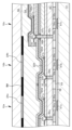
도 8은, 실시례1의 발광 소자 유닛의 모식적인 일부 단면도.
도 9는, 실시례1의 발광 소자 유닛의 변형례(1)의 모식적인 일부 단면도.
도 10A, 도 10B, 도 10C 및 도 10D는, 실시례1의 발광 소자 유닛에서의 제1 전극 및 콘택트 홀부의 배치 상태를 설명하기 위한 도면.
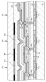
도 11은, 실시례2의 발광 소자 유닛의 모식적인 일부 단면도.
도 12는, 실시례2의 발광 소자 유닛의 변형례(1)의 모식적인 일부 단면도.
도 13은, 실시례2의 발광 소자 유닛의 변형례(2)의 모식적인 일부 단면도.
도 14는, 실시례2의 발광 소자 유닛의 변형례(3)의 모식적인 일부 단면도.
도 15는, 실시례3의 발광 소자 유닛의 모식적인 일부 단면도.
도 16은, 실시례3의 발광 소자 유닛의 변형례(1)의 모식적인 일부 단면도.
도 17은, 실시례3의 발광 소자 유닛의 변형례(2)의 모식적인 일부 단면도.
도 18은, 실시례3의 발광 소자 유닛의 변형례(3)의 모식적인 일부 단면도.
도 19A 및 도 19B는, 실시례1의 발광 소자 유닛의 제조 방법을 설명하기 위한 제1 기판 등의 모식적인 단면도.
도 20A 및 도 20B는, 도 19B에 이어, 실시례1의 발광 소자 유닛의 제조 방법을 설명하기 위한 제1 기판 등의 모식적인 단면도.
도 21은, 도 20B에 이어, 실시례1의 발광 소자 유닛의 제조 방법을 설명하기 위한 제1 기판 등의 모식적인 단면도.
도 22는, 도 21에 이어, 실시례1의 발광 소자 유닛의 제조 방법을 설명하기 위한 제1 기판 등의 모식적인 단면도.
도 23은, 도 22에 이어, 실시례1의 발광 소자 유닛의 제조 방법을 설명하기 위한 제1 기판 등의 모식적인 단면도.
도 24는, 도 23에 이어, 실시례1의 발광 소자 유닛의 제조 방법을 설명하기 위한 제1 기판 등의 모식적인 단면도.
도 25는, 도 24에 이어, 실시례1의 발광 소자 유닛의 제조 방법을 설명하기 위한 제1 기판 등의 모식적인 단면도.
도 26은, 도 25에 이어, 실시례1의 발광 소자 유닛의 제조 방법을 설명하기 위한 제1 기판 등의 모식적인 단면도.
도 27A 및 도 27B는, 본 개시에서의 표시 장치를 렌즈 교환 일안 리플렉스 타입의 디지털 스틸 카메라에 적용한 예로서, 도 27A는 디지털 스틸 카메라의 정면도, 도 27B는 디지털 스틸 카메라의 배면도.
도 28은, 본 개시에서의 표시 장치를 헤드 마운트 디스플레이에 적용한 예를 도시하는 헤드 마운트 디스플레이의 외관도.
10a : 제1 발광 소자
10b : 제2 발광 소자
10c : 제3 발광 소자
21a : 제1a 전극
21b : 제1b 전극
21c : 제1c 전극
22a : 제2a 전극
22b : 제2b 전극
22c : 제2c 전극
22d :공통 제2 전극(제2a 전극 및 제2b 전극)
23a : 제1 발광층을 포함하는 제1 유기층
23b : 제2 발광층을 포함하는 제2 유기층
23c : 제3 발광층을 포함하는 제3 유기층
23d : 제1 유기층 및 제2 유기층
24a, 24b :컬러 필터
25a, 25b, 25c :광반사층
BM :블랙 매트릭스층
31, 32, 33, 34, 35, 36, 37, 38 :층간 절연층
41 : 제1 기판
42 : 제2 기판
43 :절연층
44 :보호막
51a, 51b, 51c :게이트 전극
52 :게이트 절연막
53 :실리콘층(반도체층)
54a, 54b, 54c :채널 형성 영역
55a, 55b, 55c :소스/드레인 영역
56a, 56b, 56c, 57b, 57c, 58c, 66, 67, 68, 69 :콘택트 홀부
59a, 59b :절연막
Claims (13)
- 3개의 발광 소자를 포함하는 발광 소자 유닛으로서,
제1 발광 소자는, 제1a 전극, 제1 발광층을 포함하는 제1 유기층, 제2a 전극, 제2 발광층을 포함하는 제2 유기층, 및, 제3 발광층을 포함하는 제3 유기층의 순서로 적층되어 이루어지고,
제2 발광 소자는, 상기 제1 유기층, 제1b 전극, 상기 제2 유기층, 제2b 전극, 및, 상기 제3 유기층의 순서로 적층되어 이루어지고,
제3 발광 소자는, 상기 제1 유기층, 상기 제2 유기층, 제1c 전극, 상기 제3 유기층, 및, 제2c 전극의 순서로 적층되어 이루어지고,
상기 제1 발광 소자에 있어서, 상기 제1a 전극의 하방에 마련된 제1 광반사층에 의해 구성된 제1a 계면과, 상기 제2a 전극과 상기 제1 유기층의 계면에 의해 구성된 제2a 계면과의 사이에서, 상기 제1 발광층에서 발광한 광을 공진시켜서, 그 일부를 상기 제2a 전극으로부터 출사시키고,
상기 제2 발광 소자에 있어서, 상기 제1b 전극의 하방에 마련된 제2 광반사층에 의해 구성된 제1b 계면과, 상기 제2b 전극과 상기 제2 유기층의 계면에 의해 구성된 제2b 계면과의 사이에서, 상기 제2 발광층에서 발광한 광을 공진시켜서, 그 일부를 상기 제2b 전극으로부터 출사시키고,
상기 제3 발광 소자에 있어서, 상기 제1c 전극의 하방에 마련된 제3 광반사층에 의해 구성된 제1c 계면과, 상기 제2c 전극과 상기 제3 유기층의 계면에 의해 구성된 제2c 계면과의 사이에서, 상기 제3 발광층에서 발광한 광을 공진시켜서, 그 일부를 상기 제2c 전극으로부터 출사시키고,
상기 발광 소자 유닛의 단면시에 있어서, 상기 제2a 전극, 상기 제2b 전극, 및 상기 제2c 전극은, 서로 중합하고 있지 않는 것을 특징으로 하는 발광 소자 유닛. - 제1항에 있어서,
상기 제2a 전극, 상기 제2b 전극 및 상기 제2c 전극은, 공통의 제2 전극으로 구성되어 있는 것을 특징으로 하는 발광 소자 유닛. - 제1항에 있어서,
상기 제2a 전극, 상기 제2b 전극 및 상기 제2c 전극에는, 동일한 전위가 주어지는 것을 특징으로 하는 발광 소자 유닛. - 제1항에 있어서,
상기 제2a 전극, 상기 제2b 전극 및 상기 제2c 전극은, 투명 도전층과 반투과 도전층의 적층 구조를 갖는 것을 특징으로 하는 발광 소자 유닛. - 제4항에 있어서,
상기 투명 도전층은, 인듐과 아연의 산화물로 이루어지는 것을 특징으로 하는 발광 소자 유닛. - 제4항에 있어서,
상기 반투과 도전층은, 마그네슘 및 은의 합금으로 이루어지는 것을 특징으로 하는 발광 소자 유닛. - 제6항에 있어서,
상기 제1 발광층의 최대 발광 위치에서 상기 제1a 계면까지의 거리를 L1A, 광학 거리를 OL1A, 상기 제1 발광층의 최대 발광 위치에서 상기 제2a 계면까지의 거리를 L2A, 광학 거리를 OL2A 로 하고, m1A 및 m2A 를 정수로 하였을 때, 이하의 식(A-1), 식(A-2), 식(A-3) 및 식(A-4)을 충족시키고 있고,
상기 제2 발광층의 최대 발광 위치에서 상기 제1b 계면까지의 거리를 L1B, 광학 거리를 OL1B, 상기 제2 발광층의 최대 발광 위치에서 상기 제2b 계면까지의 거리를 L2B, 광학 거리를 OL2B 로 하고, m1B 및 m2B 를 정수로 하였을 때, 이하의 식(B-1), 식(B-2), 식(B-3) 및 식(B-4)을 충족시키고 있고,
상기 제3 발광층의 최대 발광 위치에서 상기 제1c 계면까지의 거리를 L1C, 광학 거리를 OL1C, 상기 제3 발광층의 최대 발광 위치에서 상기 제2c 계면까지의 거리를 L2C, 광학 거리를 OL2C 로 하고, m1C 및 m2C 를 정수로 하였을 때, 이하의 식(C-1), 식(C-2), 식(C-3) 및 식(C-4)을 충족시키고 있는 것을 특징으로 하는 발광 소자 유닛.
0.7{-Φ1A/(2π)+m1A}≤2×OL1A/λA≤1.2{-Φ1A/(2π)+m1A} (A-1)
0.7{-Φ2A/(2π)+m2A}≤2×OL2A/λA≤1.2{-Φ2A/(2π)+m2A} (A-2)
L1A<L2A (A-3)
m1A<m2A (A-4)
0.7{-Φ1B/(2π)+m1B}≤2×OL1B/λB≤1.2{-Φ1B/(2π)+m1B} (B-1)
0.7{-Φ2B/(2π)+m2B}≤2×OL2B/λB≤1.2{-Φ2B/(2π)+m2B} (B-2)
L1B<L2B (B-3)
m1B<m2B (B-4)
0.7{-Φ1C/(2π)+m1C}≤2×OL1C/λC≤1.2{-Φ1C/(2π)+m1C} (C-1)
0.7{-Φ2C/(2π)+m2C}≤2×OL2C/λC≤1.2{-Φ2C/(2π)+m2C} (C-2)
L1C<L2C (C-3)
m1C<m2C (C-4)
여기서,
λA : 상기 제1 발광층에서 발생한 광의 스펙트럼의 최대 피크 파장(또는, 상기 제1 발광층에서 발생한 광 내의 파장)
Φ1A : 상기 제1a 계면에서 반사하는 광의 위상 시프트량(단위:라디안)
단, -2π<Φ1A≤0
Φ2A : 상기 제2a 계면에서 반사되는 광의 위상 시프트량(단위:라디안)
단, -2π<Φ2A≤0
λB : 상기 제2 발광층에서 발생한 광의 스펙트럼의 최대 피크 파장(또는, 제2 발광층에서 발생한 광 내의 파장)
Φ1B: : 상기 제1b 계면에서 반사되는 광의 위상 시프트량(단위:라디안)
단, -2π<Φ1B≤0
Φ2B: : 상기 제2b 계면에서 반사되는 광의 위상 시프트량(단위:라디안)
단, -2π<Φ2B≤0
λC : 상기 제3 발광층에서 발생한 광의 스펙트럼의 최대 피크 파장(또는, 상기 제3 발광층에서 발생한 광 내의 파장)
Φ1C : 상기 제1c 계면에서 반사되는 광의 위상 시프트량(단위:라디안)
단, -2π<Φ1C≤0
Φ2C : 상기 제2c 계면에서 반사되는 광의 위상 시프트량(단위:라디안)
단, -2π<Φ2C≤0
이다. - 제7항에 있어서,
m1A=0, m2A =1, m1B=0, m2B =1, m1C=0, m2C =1인 것을 특징으로 하는 발광 소자 유닛. - 제1항 내지 제8항 중 어느 한 항에 있어서,
상기 발광 소자 유닛의 단면시에 있어서, 상기 제1a 전극, 상기 제1b 전극, 및 상기 제1c 전극은, 서로 중합하고 있지 않는 것을 특징으로 하는 발광 소자 유닛. - 삭제
- 삭제
- 삭제
- 삭제
Priority Applications (1)
| Application Number | Priority Date | Filing Date | Title |
|---|---|---|---|
| KR1020257011521A KR20250053986A (ko) | 2018-03-06 | 2019-03-01 | 발광 소자 유닛 |
Applications Claiming Priority (3)
| Application Number | Priority Date | Filing Date | Title |
|---|---|---|---|
| JP2018039598 | 2018-03-06 | ||
| JPJP-P-2018-039598 | 2018-03-06 | ||
| PCT/JP2019/008109 WO2019172121A1 (ja) | 2018-03-06 | 2019-03-01 | 発光素子ユニット |
Related Child Applications (1)
| Application Number | Title | Priority Date | Filing Date |
|---|---|---|---|
| KR1020257011521A Division KR20250053986A (ko) | 2018-03-06 | 2019-03-01 | 발광 소자 유닛 |
Publications (2)
| Publication Number | Publication Date |
|---|---|
| KR20200127184A KR20200127184A (ko) | 2020-11-10 |
| KR102795816B1 true KR102795816B1 (ko) | 2025-04-16 |
Family
ID=67846053
Family Applications (2)
| Application Number | Title | Priority Date | Filing Date |
|---|---|---|---|
| KR1020207024933A Active KR102795816B1 (ko) | 2018-03-06 | 2019-03-01 | 발광 소자 유닛 |
| KR1020257011521A Pending KR20250053986A (ko) | 2018-03-06 | 2019-03-01 | 발광 소자 유닛 |
Family Applications After (1)
| Application Number | Title | Priority Date | Filing Date |
|---|---|---|---|
| KR1020257011521A Pending KR20250053986A (ko) | 2018-03-06 | 2019-03-01 | 발광 소자 유닛 |
Country Status (6)
| Country | Link |
|---|---|
| US (2) | US11362306B2 (ko) |
| JP (3) | JP7261220B2 (ko) |
| KR (2) | KR102795816B1 (ko) |
| CN (1) | CN111819909B (ko) |
| DE (1) | DE112019001178T5 (ko) |
| WO (1) | WO2019172121A1 (ko) |
Families Citing this family (5)
| Publication number | Priority date | Publication date | Assignee | Title |
|---|---|---|---|---|
| KR102676592B1 (ko) * | 2019-01-18 | 2024-06-21 | 삼성디스플레이 주식회사 | 표시 장치 및 그 제조 방법 |
| CN110854302B (zh) * | 2019-10-31 | 2021-02-26 | 深圳市华星光电半导体显示技术有限公司 | Oled显示面板及其制备方法、oled显示装置 |
| KR102670023B1 (ko) * | 2020-03-04 | 2024-05-27 | 주식회사 디비하이텍 | 유기발광 표시장치 및 제조방법 |
| JP7176552B2 (ja) * | 2020-08-31 | 2022-11-22 | セイコーエプソン株式会社 | 電気光学装置および電子機器 |
| KR200497443Y1 (ko) * | 2021-10-27 | 2023-11-09 | 김진성 | 보조 투명 디스플레이 장치 및 이를 포함하는 언더 디스플레이 카메라 |
Citations (2)
| Publication number | Priority date | Publication date | Assignee | Title |
|---|---|---|---|---|
| JP2009049135A (ja) * | 2007-08-17 | 2009-03-05 | Sony Corp | 表示装置 |
| US20130341659A1 (en) * | 2012-06-22 | 2013-12-26 | Industrial Technology Research Institute | Display panel |
Family Cites Families (68)
| Publication number | Priority date | Publication date | Assignee | Title |
|---|---|---|---|---|
| US5424560A (en) * | 1994-05-31 | 1995-06-13 | Motorola, Inc. | Integrated multicolor organic led array |
| US5707745A (en) * | 1994-12-13 | 1998-01-13 | The Trustees Of Princeton University | Multicolor organic light emitting devices |
| AU5621598A (en) * | 1996-12-23 | 1998-07-17 | Trustees Of Princeton University, The | Light emitting articles with light reflecting structures |
| US5917280A (en) * | 1997-02-03 | 1999-06-29 | The Trustees Of Princeton University | Stacked organic light emitting devices |
| US5953587A (en) * | 1997-11-24 | 1999-09-14 | The Trustees Of Princeton University | Method for deposition and patterning of organic thin film |
| JPH11312585A (ja) * | 1998-04-28 | 1999-11-09 | Tdk Corp | 有機el素子 |
| JP4182467B2 (ja) * | 2001-12-27 | 2008-11-19 | セイコーエプソン株式会社 | 回路基板、電気光学装置及び電子機器 |
| JP4378767B2 (ja) * | 2002-09-26 | 2009-12-09 | セイコーエプソン株式会社 | 発光装置及び電子機器 |
| KR101079820B1 (ko) * | 2003-09-19 | 2011-11-04 | 소니 가부시키가이샤 | 유기 발광 장치 및 그 제조 방법과 표시 장치 |
| KR100635056B1 (ko) * | 2004-02-19 | 2006-10-16 | 삼성에스디아이 주식회사 | 유기전계 발광표시장치의 제조방법 |
| KR100721554B1 (ko) * | 2004-07-22 | 2007-05-23 | 삼성에스디아이 주식회사 | 유기 전계 발광 소자 및 그의 제조 방법 |
| JP2006278257A (ja) * | 2005-03-30 | 2006-10-12 | Sony Corp | 有機発光装置およびその製造方法 |
| JP4507964B2 (ja) | 2005-04-15 | 2010-07-21 | ソニー株式会社 | 表示装置および表示装置の製造方法 |
| JP4677822B2 (ja) * | 2005-04-22 | 2011-04-27 | セイコーエプソン株式会社 | エレクトロルミネッセンス装置、エレクトロルミネッセンス装置の製造方法、電子機器 |
| JP2007012359A (ja) * | 2005-06-29 | 2007-01-18 | Hitachi Displays Ltd | 有機el表示装置 |
| US7327081B2 (en) * | 2005-08-31 | 2008-02-05 | Chunghwa Picture Tubes, Ltd. | Stacked organic electroluminescent device and method for manufacturing thereof |
| JP4462155B2 (ja) * | 2005-09-27 | 2010-05-12 | セイコーエプソン株式会社 | 発光装置、発光装置の製造方法および電子機器 |
| JP5147320B2 (ja) * | 2006-07-21 | 2013-02-20 | 株式会社半導体エネルギー研究所 | 半導体装置 |
| US7498603B2 (en) * | 2006-12-06 | 2009-03-03 | General Electric Company | Color tunable illumination source and method for controlled illumination |
| KR101429933B1 (ko) * | 2007-07-03 | 2014-08-14 | 엘지디스플레이 주식회사 | 유기전계발광표시장치 및 그 제조방법 |
| JP2009064703A (ja) | 2007-09-07 | 2009-03-26 | Sony Corp | 有機発光表示装置 |
| US8063552B2 (en) * | 2007-10-22 | 2011-11-22 | Global Oled Technology Llc | LED device having improved light output |
| KR101458905B1 (ko) * | 2008-02-12 | 2014-11-07 | 삼성디스플레이 주식회사 | 유기 발광 표시 장치 및 그 제조 방법 |
| JP5522991B2 (ja) * | 2008-07-11 | 2014-06-18 | キヤノン株式会社 | 有機el表示装置 |
| JP2010056075A (ja) * | 2008-07-29 | 2010-03-11 | Sony Corp | 発光素子及び有機エレクトロルミネッセンス表示装置 |
| KR101582937B1 (ko) * | 2008-12-02 | 2016-01-08 | 삼성디스플레이 주식회사 | 유기 발광 표시 장치 및 그 제조 방법 |
| KR20100071539A (ko) * | 2008-12-19 | 2010-06-29 | 삼성전자주식회사 | 유기 발광 표시 장치 및 그 제조 방법 |
| JP5463882B2 (ja) * | 2009-12-01 | 2014-04-09 | ソニー株式会社 | 発光素子及びその製造方法 |
| JP5759760B2 (ja) * | 2011-03-16 | 2015-08-05 | 株式会社Joled | 表示装置および電子機器 |
| TWI562424B (en) * | 2011-03-25 | 2016-12-11 | Semiconductor Energy Lab Co Ltd | Light-emitting panel, light-emitting device, and method for manufacturing the light-emitting panel |
| JP5644677B2 (ja) * | 2011-05-31 | 2014-12-24 | セイコーエプソン株式会社 | 有機el装置 |
| KR101825642B1 (ko) * | 2011-08-18 | 2018-02-06 | 삼성디스플레이 주식회사 | 유기 발광 표시 장치 및 그 제조 방법 |
| KR101407309B1 (ko) * | 2011-11-15 | 2014-06-16 | 엘지디스플레이 주식회사 | 유기 전계 발광 표시 패널 및 그의 제조 방법 |
| TW201324761A (zh) * | 2011-12-08 | 2013-06-16 | Au Optronics Corp | 電激發光顯示面板之畫素結構 |
| KR20230015519A (ko) * | 2012-10-30 | 2023-01-31 | 가부시키가이샤 한도오따이 에네루기 켄큐쇼 | 발광 패널, 디스플레이 장치, 및 발광 패널을 제작하는 방법 |
| KR102037850B1 (ko) * | 2013-02-27 | 2019-10-29 | 엘지디스플레이 주식회사 | 유기 발광 표시 장치 및 그 제조 방법 |
| KR102178256B1 (ko) * | 2013-03-27 | 2020-11-12 | 가부시키가이샤 한도오따이 에네루기 켄큐쇼 | 발광 소자, 발광 장치, 전자 기기, 및 조명 장치 |
| JP6263337B2 (ja) * | 2013-05-31 | 2018-01-17 | 株式会社ジャパンディスプレイ | 表示装置及びその製造方法 |
| KR102090709B1 (ko) * | 2013-05-31 | 2020-03-19 | 삼성디스플레이 주식회사 | 백색 유기 발광 표시 장치 |
| KR102053443B1 (ko) * | 2013-10-23 | 2019-12-06 | 엘지디스플레이 주식회사 | 유기전계발광소자 |
| JP6656817B2 (ja) * | 2014-04-25 | 2020-03-04 | 株式会社半導体エネルギー研究所 | 発光装置 |
| JP2016048602A (ja) * | 2014-08-27 | 2016-04-07 | 株式会社ジャパンディスプレイ | 表示装置 |
| KR102226726B1 (ko) * | 2014-09-30 | 2021-03-12 | 엘지디스플레이 주식회사 | 유기발광표시장치 |
| JP6629505B2 (ja) * | 2014-11-18 | 2020-01-15 | 株式会社Joled | 発光素子およびそれを備えた表示装置 |
| JP6358946B2 (ja) * | 2014-12-18 | 2018-07-18 | 株式会社ジャパンディスプレイ | 有機el表示装置 |
| KR102369674B1 (ko) * | 2015-02-17 | 2022-03-04 | 삼성디스플레이 주식회사 | 디스플레이 장치, 및 이를 포함하는 전자 기기 |
| JP2016195070A (ja) | 2015-04-01 | 2016-11-17 | ソニー株式会社 | 表示装置、表示装置の製造方法、及び、電子機器 |
| JP2017027872A (ja) * | 2015-07-27 | 2017-02-02 | ソニー株式会社 | 表示装置 |
| JP6601047B2 (ja) * | 2015-08-07 | 2019-11-06 | ソニー株式会社 | 発光素子及びその製造方法、並びに、表示装置 |
| JP2017062884A (ja) | 2015-09-24 | 2017-03-30 | ソニー株式会社 | 表示装置及び発光装置 |
| JP2017062941A (ja) | 2015-09-25 | 2017-03-30 | ソニー株式会社 | 表示装置及びその製造方法 |
| KR102406606B1 (ko) * | 2015-10-08 | 2022-06-09 | 삼성디스플레이 주식회사 | 유기 발광 소자, 이를 포함하는 유기 발광 표시 장치, 및 이의 제조 방법 |
| KR102626853B1 (ko) * | 2015-10-30 | 2024-01-18 | 삼성디스플레이 주식회사 | 유기 발광 표시 장치 |
| US10170521B2 (en) * | 2015-12-30 | 2019-01-01 | Lg Display Co., Ltd. | Organic light-emitting diode display device |
| US10797113B2 (en) * | 2016-01-25 | 2020-10-06 | Semiconductor Energy Laboratory Co., Ltd. | Light-emitting device with layered electrode structures |
| JP2017174553A (ja) * | 2016-03-22 | 2017-09-28 | 株式会社ジャパンディスプレイ | 表示装置 |
| KR102457437B1 (ko) * | 2016-03-31 | 2022-10-24 | 소니그룹주식회사 | 표시 장치 및 전자 기기 |
| US10256277B2 (en) * | 2016-04-11 | 2019-04-09 | Abl Ip Holding Llc | Luminaire utilizing a transparent organic light emitting device display |
| US10141377B2 (en) * | 2016-07-29 | 2018-11-27 | Lg Display Co., Ltd. | Electroluminescent display device |
| WO2018061987A1 (ja) * | 2016-09-28 | 2018-04-05 | シャープ株式会社 | 表示装置およびその製造方法 |
| KR102758804B1 (ko) * | 2016-10-31 | 2025-01-23 | 엘지디스플레이 주식회사 | 발광 영역들을 포함하는 디스플레이 장치 |
| KR102642304B1 (ko) * | 2016-11-28 | 2024-02-28 | 삼성전자주식회사 | 광전자 소자 및 전자 장치 |
| KR102656795B1 (ko) * | 2016-11-30 | 2024-04-11 | 엘지디스플레이 주식회사 | 유기발광 표시장치와 그의 제조방법 |
| KR102611794B1 (ko) * | 2016-11-30 | 2023-12-07 | 엘지디스플레이 주식회사 | 유기발광 표시장치와 그의 제조방법 |
| US10330993B2 (en) * | 2016-12-23 | 2019-06-25 | Semiconductor Energy Laboratory Co., Ltd. | Display device |
| KR102783429B1 (ko) * | 2017-01-25 | 2025-03-18 | 삼성디스플레이 주식회사 | 표시 장치 |
| CN109216329B (zh) * | 2017-07-07 | 2020-09-08 | 鸿富锦精密工业(深圳)有限公司 | 微型led显示面板及其制备方法 |
| KR102513769B1 (ko) * | 2018-11-29 | 2023-03-23 | 엘지디스플레이 주식회사 | 전계 발광 표시 장치 |
-
2019
- 2019-03-01 KR KR1020207024933A patent/KR102795816B1/ko active Active
- 2019-03-01 CN CN201980015710.2A patent/CN111819909B/zh active Active
- 2019-03-01 KR KR1020257011521A patent/KR20250053986A/ko active Pending
- 2019-03-01 WO PCT/JP2019/008109 patent/WO2019172121A1/ja not_active Ceased
- 2019-03-01 JP JP2020504986A patent/JP7261220B2/ja active Active
- 2019-03-01 US US16/970,280 patent/US11362306B2/en active Active
- 2019-03-01 DE DE112019001178.2T patent/DE112019001178T5/de active Pending
-
2022
- 2022-05-16 US US17/745,306 patent/US12041813B2/en active Active
- 2022-07-04 JP JP2022107996A patent/JP7356545B2/ja active Active
- 2022-12-13 JP JP2022198911A patent/JP7509860B2/ja active Active
Patent Citations (2)
| Publication number | Priority date | Publication date | Assignee | Title |
|---|---|---|---|---|
| JP2009049135A (ja) * | 2007-08-17 | 2009-03-05 | Sony Corp | 表示装置 |
| US20130341659A1 (en) * | 2012-06-22 | 2013-12-26 | Industrial Technology Research Institute | Display panel |
Also Published As
| Publication number | Publication date |
|---|---|
| US20230006176A1 (en) | 2023-01-05 |
| DE112019001178T5 (de) | 2020-12-10 |
| JPWO2019172121A1 (ja) | 2021-04-08 |
| KR20250053986A (ko) | 2025-04-22 |
| JP7261220B2 (ja) | 2023-04-19 |
| JP2023036701A (ja) | 2023-03-14 |
| KR20200127184A (ko) | 2020-11-10 |
| US12041813B2 (en) | 2024-07-16 |
| US20210143367A1 (en) | 2021-05-13 |
| JP7356545B2 (ja) | 2023-10-04 |
| JP2022128510A (ja) | 2022-09-01 |
| WO2019172121A1 (ja) | 2019-09-12 |
| JP7509860B2 (ja) | 2024-07-02 |
| CN111819909B (zh) | 2025-01-17 |
| CN111819909A (zh) | 2020-10-23 |
| US11362306B2 (en) | 2022-06-14 |
Similar Documents
| Publication | Publication Date | Title |
|---|---|---|
| KR102796410B1 (ko) | 발광 소자 및 표시 장치 | |
| US20230126274A1 (en) | Light emission element and display device | |
| KR102752849B1 (ko) | 표시 장치 | |
| US12069880B2 (en) | Light emitting element, method for manufacturing the same, and display device | |
| CN108029175B (zh) | 显示装置以及用于制造其的方法 | |
| JP6844620B2 (ja) | 表示装置 | |
| KR102795816B1 (ko) | 발광 소자 유닛 | |
| WO2021261262A1 (ja) | 表示装置 | |
| JP7525403B2 (ja) | 表示装置 | |
| WO2020110944A1 (ja) | 発光素子、表示装置及び電子機器 |
Legal Events
| Date | Code | Title | Description |
|---|---|---|---|
| PA0105 | International application |
St.27 status event code: A-0-1-A10-A15-nap-PA0105 |
|
| PG1501 | Laying open of application |
St.27 status event code: A-1-1-Q10-Q12-nap-PG1501 |
|
| PA0201 | Request for examination |
St.27 status event code: A-1-2-D10-D11-exm-PA0201 |
|
| P22-X000 | Classification modified |
St.27 status event code: A-2-2-P10-P22-nap-X000 |
|
| P22-X000 | Classification modified |
St.27 status event code: A-2-2-P10-P22-nap-X000 |
|
| E902 | Notification of reason for refusal | ||
| PE0902 | Notice of grounds for rejection |
St.27 status event code: A-1-2-D10-D21-exm-PE0902 |
|
| E13-X000 | Pre-grant limitation requested |
St.27 status event code: A-2-3-E10-E13-lim-X000 |
|
| P11-X000 | Amendment of application requested |
St.27 status event code: A-2-2-P10-P11-nap-X000 |
|
| P13-X000 | Application amended |
St.27 status event code: A-2-2-P10-P13-nap-X000 |
|
| E701 | Decision to grant or registration of patent right | ||
| PE0701 | Decision of registration |
St.27 status event code: A-1-2-D10-D22-exm-PE0701 |
|
| PA0104 | Divisional application for international application |
St.27 status event code: A-0-1-A10-A16-div-PA0104 |
|
| PR0701 | Registration of establishment |
St.27 status event code: A-2-4-F10-F11-exm-PR0701 |
|
| PR1002 | Payment of registration fee |
St.27 status event code: A-2-2-U10-U12-oth-PR1002 |
|
| PG1601 | Publication of registration |
St.27 status event code: A-4-4-Q10-Q13-nap-PG1601 |
|
| P22-X000 | Classification modified |
St.27 status event code: A-4-4-P10-P22-nap-X000 |