KR102795816B1 - Light-emitting element unit - Google Patents
Light-emitting element unit Download PDFInfo
- Publication number
- KR102795816B1 KR102795816B1 KR1020207024933A KR20207024933A KR102795816B1 KR 102795816 B1 KR102795816 B1 KR 102795816B1 KR 1020207024933 A KR1020207024933 A KR 1020207024933A KR 20207024933 A KR20207024933 A KR 20207024933A KR 102795816 B1 KR102795816 B1 KR 102795816B1
- Authority
- KR
- South Korea
- Prior art keywords
- light
- electrode
- layer
- emitting element
- emitting
- Prior art date
- Legal status (The legal status is an assumption and is not a legal conclusion. Google has not performed a legal analysis and makes no representation as to the accuracy of the status listed.)
- Active
Links
Images


Classifications
-
- H—ELECTRICITY
- H10—SEMICONDUCTOR DEVICES; ELECTRIC SOLID-STATE DEVICES NOT OTHERWISE PROVIDED FOR
- H10K—ORGANIC ELECTRIC SOLID-STATE DEVICES
- H10K59/00—Integrated devices, or assemblies of multiple devices, comprising at least one organic light-emitting element covered by group H10K50/00
- H10K59/30—Devices specially adapted for multicolour light emission
- H10K59/32—Stacked devices having two or more layers, each emitting at different wavelengths
-
- G—PHYSICS
- G09—EDUCATION; CRYPTOGRAPHY; DISPLAY; ADVERTISING; SEALS
- G09F—DISPLAYING; ADVERTISING; SIGNS; LABELS OR NAME-PLATES; SEALS
- G09F9/00—Indicating arrangements for variable information in which the information is built-up on a support by selection or combination of individual elements
- G09F9/30—Indicating arrangements for variable information in which the information is built-up on a support by selection or combination of individual elements in which the desired character or characters are formed by combining individual elements
- G09F9/302—Indicating arrangements for variable information in which the information is built-up on a support by selection or combination of individual elements in which the desired character or characters are formed by combining individual elements characterised by the form or geometrical disposition of the individual elements
-
- H—ELECTRICITY
- H05—ELECTRIC TECHNIQUES NOT OTHERWISE PROVIDED FOR
- H05B—ELECTRIC HEATING; ELECTRIC LIGHT SOURCES NOT OTHERWISE PROVIDED FOR; CIRCUIT ARRANGEMENTS FOR ELECTRIC LIGHT SOURCES, IN GENERAL
- H05B33/00—Electroluminescent light sources
- H05B33/12—Light sources with substantially two-dimensional radiating surfaces
- H05B33/22—Light sources with substantially two-dimensional radiating surfaces characterised by the chemical or physical composition or the arrangement of auxiliary dielectric or reflective layers
- H05B33/24—Light sources with substantially two-dimensional radiating surfaces characterised by the chemical or physical composition or the arrangement of auxiliary dielectric or reflective layers of metallic reflective layers
-
- H—ELECTRICITY
- H05—ELECTRIC TECHNIQUES NOT OTHERWISE PROVIDED FOR
- H05B—ELECTRIC HEATING; ELECTRIC LIGHT SOURCES NOT OTHERWISE PROVIDED FOR; CIRCUIT ARRANGEMENTS FOR ELECTRIC LIGHT SOURCES, IN GENERAL
- H05B33/00—Electroluminescent light sources
- H05B33/12—Light sources with substantially two-dimensional radiating surfaces
- H05B33/26—Light sources with substantially two-dimensional radiating surfaces characterised by the composition or arrangement of the conductive material used as an electrode
- H05B33/28—Light sources with substantially two-dimensional radiating surfaces characterised by the composition or arrangement of the conductive material used as an electrode of translucent electrodes
-
- H—ELECTRICITY
- H10—SEMICONDUCTOR DEVICES; ELECTRIC SOLID-STATE DEVICES NOT OTHERWISE PROVIDED FOR
- H10K—ORGANIC ELECTRIC SOLID-STATE DEVICES
- H10K50/00—Organic light-emitting devices
- H10K50/10—OLEDs or polymer light-emitting diodes [PLED]
- H10K50/11—OLEDs or polymer light-emitting diodes [PLED] characterised by the electroluminescent [EL] layers
- H10K50/125—OLEDs or polymer light-emitting diodes [PLED] characterised by the electroluminescent [EL] layers specially adapted for multicolour light emission, e.g. for emitting white light
- H10K50/13—OLEDs or polymer light-emitting diodes [PLED] characterised by the electroluminescent [EL] layers specially adapted for multicolour light emission, e.g. for emitting white light comprising stacked EL layers within one EL unit
- H10K50/131—OLEDs or polymer light-emitting diodes [PLED] characterised by the electroluminescent [EL] layers specially adapted for multicolour light emission, e.g. for emitting white light comprising stacked EL layers within one EL unit with spacer layers between the electroluminescent layers
-
- H—ELECTRICITY
- H10—SEMICONDUCTOR DEVICES; ELECTRIC SOLID-STATE DEVICES NOT OTHERWISE PROVIDED FOR
- H10K—ORGANIC ELECTRIC SOLID-STATE DEVICES
- H10K50/00—Organic light-emitting devices
- H10K50/80—Constructional details
- H10K50/805—Electrodes
- H10K50/82—Cathodes
- H10K50/822—Cathodes characterised by their shape
-
- H—ELECTRICITY
- H10—SEMICONDUCTOR DEVICES; ELECTRIC SOLID-STATE DEVICES NOT OTHERWISE PROVIDED FOR
- H10K—ORGANIC ELECTRIC SOLID-STATE DEVICES
- H10K50/00—Organic light-emitting devices
- H10K50/80—Constructional details
- H10K50/805—Electrodes
- H10K50/82—Cathodes
- H10K50/828—Transparent cathodes, e.g. comprising thin metal layers
-
- H—ELECTRICITY
- H10—SEMICONDUCTOR DEVICES; ELECTRIC SOLID-STATE DEVICES NOT OTHERWISE PROVIDED FOR
- H10K—ORGANIC ELECTRIC SOLID-STATE DEVICES
- H10K50/00—Organic light-emitting devices
- H10K50/80—Constructional details
- H10K50/84—Passivation; Containers; Encapsulations
- H10K50/844—Encapsulations
-
- H—ELECTRICITY
- H10—SEMICONDUCTOR DEVICES; ELECTRIC SOLID-STATE DEVICES NOT OTHERWISE PROVIDED FOR
- H10K—ORGANIC ELECTRIC SOLID-STATE DEVICES
- H10K59/00—Integrated devices, or assemblies of multiple devices, comprising at least one organic light-emitting element covered by group H10K50/00
- H10K59/10—OLED displays
- H10K59/12—Active-matrix OLED [AMOLED] displays
- H10K59/121—Active-matrix OLED [AMOLED] displays characterised by the geometry or disposition of pixel elements
-
- H—ELECTRICITY
- H10—SEMICONDUCTOR DEVICES; ELECTRIC SOLID-STATE DEVICES NOT OTHERWISE PROVIDED FOR
- H10K—ORGANIC ELECTRIC SOLID-STATE DEVICES
- H10K59/00—Integrated devices, or assemblies of multiple devices, comprising at least one organic light-emitting element covered by group H10K50/00
- H10K59/10—OLED displays
- H10K59/12—Active-matrix OLED [AMOLED] displays
- H10K59/123—Connection of the pixel electrodes to the thin film transistors [TFT]
-
- H—ELECTRICITY
- H10—SEMICONDUCTOR DEVICES; ELECTRIC SOLID-STATE DEVICES NOT OTHERWISE PROVIDED FOR
- H10K—ORGANIC ELECTRIC SOLID-STATE DEVICES
- H10K59/00—Integrated devices, or assemblies of multiple devices, comprising at least one organic light-emitting element covered by group H10K50/00
- H10K59/30—Devices specially adapted for multicolour light emission
- H10K59/38—Devices specially adapted for multicolour light emission comprising colour filters or colour changing media [CCM]
-
- H—ELECTRICITY
- H10—SEMICONDUCTOR DEVICES; ELECTRIC SOLID-STATE DEVICES NOT OTHERWISE PROVIDED FOR
- H10K—ORGANIC ELECTRIC SOLID-STATE DEVICES
- H10K59/00—Integrated devices, or assemblies of multiple devices, comprising at least one organic light-emitting element covered by group H10K50/00
- H10K59/80—Constructional details
- H10K59/805—Electrodes
- H10K59/8051—Anodes
- H10K59/80515—Anodes characterised by their shape
-
- H—ELECTRICITY
- H10—SEMICONDUCTOR DEVICES; ELECTRIC SOLID-STATE DEVICES NOT OTHERWISE PROVIDED FOR
- H10K—ORGANIC ELECTRIC SOLID-STATE DEVICES
- H10K59/00—Integrated devices, or assemblies of multiple devices, comprising at least one organic light-emitting element covered by group H10K50/00
- H10K59/80—Constructional details
- H10K59/805—Electrodes
- H10K59/8051—Anodes
- H10K59/80517—Multilayers, e.g. transparent multilayers
-
- H—ELECTRICITY
- H10—SEMICONDUCTOR DEVICES; ELECTRIC SOLID-STATE DEVICES NOT OTHERWISE PROVIDED FOR
- H10K—ORGANIC ELECTRIC SOLID-STATE DEVICES
- H10K59/00—Integrated devices, or assemblies of multiple devices, comprising at least one organic light-emitting element covered by group H10K50/00
- H10K59/80—Constructional details
- H10K59/805—Electrodes
- H10K59/8052—Cathodes
- H10K59/80521—Cathodes characterised by their shape
-
- H—ELECTRICITY
- H10—SEMICONDUCTOR DEVICES; ELECTRIC SOLID-STATE DEVICES NOT OTHERWISE PROVIDED FOR
- H10K—ORGANIC ELECTRIC SOLID-STATE DEVICES
- H10K59/00—Integrated devices, or assemblies of multiple devices, comprising at least one organic light-emitting element covered by group H10K50/00
- H10K59/80—Constructional details
- H10K59/805—Electrodes
- H10K59/8052—Cathodes
- H10K59/80524—Transparent cathodes, e.g. comprising thin metal layers
-
- H—ELECTRICITY
- H10—SEMICONDUCTOR DEVICES; ELECTRIC SOLID-STATE DEVICES NOT OTHERWISE PROVIDED FOR
- H10K—ORGANIC ELECTRIC SOLID-STATE DEVICES
- H10K59/00—Integrated devices, or assemblies of multiple devices, comprising at least one organic light-emitting element covered by group H10K50/00
- H10K59/80—Constructional details
- H10K59/87—Passivation; Containers; Encapsulations
- H10K59/873—Encapsulations
-
- H—ELECTRICITY
- H10—SEMICONDUCTOR DEVICES; ELECTRIC SOLID-STATE DEVICES NOT OTHERWISE PROVIDED FOR
- H10K—ORGANIC ELECTRIC SOLID-STATE DEVICES
- H10K59/00—Integrated devices, or assemblies of multiple devices, comprising at least one organic light-emitting element covered by group H10K50/00
- H10K59/80—Constructional details
- H10K59/875—Arrangements for extracting light from the devices
- H10K59/876—Arrangements for extracting light from the devices comprising a resonant cavity structure, e.g. Bragg reflector pair
-
- H—ELECTRICITY
- H10—SEMICONDUCTOR DEVICES; ELECTRIC SOLID-STATE DEVICES NOT OTHERWISE PROVIDED FOR
- H10K—ORGANIC ELECTRIC SOLID-STATE DEVICES
- H10K59/00—Integrated devices, or assemblies of multiple devices, comprising at least one organic light-emitting element covered by group H10K50/00
- H10K59/80—Constructional details
- H10K59/875—Arrangements for extracting light from the devices
- H10K59/878—Arrangements for extracting light from the devices comprising reflective means
-
- H—ELECTRICITY
- H10—SEMICONDUCTOR DEVICES; ELECTRIC SOLID-STATE DEVICES NOT OTHERWISE PROVIDED FOR
- H10K—ORGANIC ELECTRIC SOLID-STATE DEVICES
- H10K2102/00—Constructional details relating to the organic devices covered by this subclass
- H10K2102/10—Transparent electrodes, e.g. using graphene
- H10K2102/101—Transparent electrodes, e.g. using graphene comprising transparent conductive oxides [TCO]
- H10K2102/103—Transparent electrodes, e.g. using graphene comprising transparent conductive oxides [TCO] comprising indium oxides, e.g. ITO
-
- H—ELECTRICITY
- H10—SEMICONDUCTOR DEVICES; ELECTRIC SOLID-STATE DEVICES NOT OTHERWISE PROVIDED FOR
- H10K—ORGANIC ELECTRIC SOLID-STATE DEVICES
- H10K50/00—Organic light-emitting devices
- H10K50/10—OLEDs or polymer light-emitting diodes [PLED]
- H10K50/11—OLEDs or polymer light-emitting diodes [PLED] characterised by the electroluminescent [EL] layers
- H10K50/125—OLEDs or polymer light-emitting diodes [PLED] characterised by the electroluminescent [EL] layers specially adapted for multicolour light emission, e.g. for emitting white light
- H10K50/13—OLEDs or polymer light-emitting diodes [PLED] characterised by the electroluminescent [EL] layers specially adapted for multicolour light emission, e.g. for emitting white light comprising stacked EL layers within one EL unit
Landscapes
- Physics & Mathematics (AREA)
- Engineering & Computer Science (AREA)
- Microelectronics & Electronic Packaging (AREA)
- Optics & Photonics (AREA)
- Geometry (AREA)
- Electroluminescent Light Sources (AREA)
- Devices For Indicating Variable Information By Combining Individual Elements (AREA)
- Optical Filters (AREA)
- General Physics & Mathematics (AREA)
- Theoretical Computer Science (AREA)
Abstract
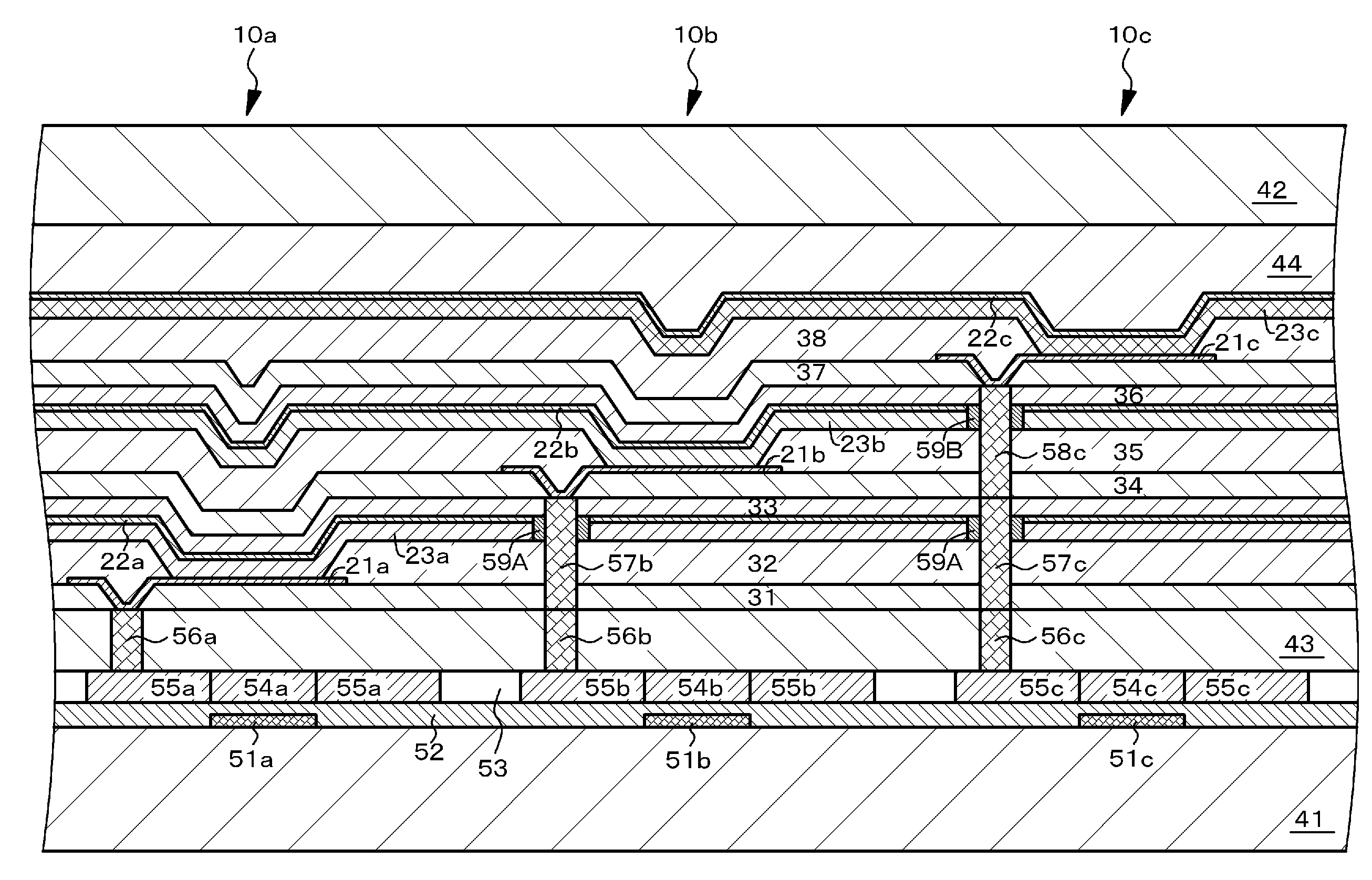
발광 소자 유닛은, 3개의 발광 소자로 구성되어 있고, 제1 발광 소자(10a)는, 제1a 전극(21a), 제1 발광층을 포함하는 제1 유기층(23a), 제2a 전극(22a), 제2 발광층을 포함하는 제2 유기층(23b), 및, 제3 발광층을 포함하는 제3 유기층(23c)이 적층되어 이루어지며, 제2 발광 소자(10b)는, 제1 유기층(23a), 제1b 전극(21b), 제2 유기층(23b), 제2b 전극(22b), 및, 제3 유기층(23c)이 적층되어 이루어지며, 제3 발광 소자(10c)는, 제1 유기층(23a), 제2 유기층(23b), 제1c 전극(21c), 제3 유기층(23c), 및, 제2c 전극(22c)이 적층되어 이루어진다. The light emitting element unit is composed of three light emitting elements, and the first light emitting element (10a) is formed by laminating a first a electrode (21a), a first organic layer (23a) including a first light emitting layer, a second a electrode (22a), a second organic layer (23b) including a second light emitting layer, and a third organic layer (23c) including a third light emitting layer, and the second light emitting element (10b) is formed by laminating a first organic layer (23a), a first b electrode (21b), a second organic layer (23b), a second b electrode (22b), and a third organic layer (23c), and the third light emitting element (10c) is formed by laminating a first organic layer (23a), a second organic layer (23b), a first c electrode (21c), a third organic layer (23c), and a second c electrode (22c).
Description
본 개시는, 발광 소자 유닛에 관한 것이다. The present disclosure relates to a light emitting element unit.
근래, 모니터 장치 등의 직시형 디스플레이 뿐만 아니라, 수 미크론의 화소 피치가 요구되는 초소형 디스플레이(마이크로 디스플레이)에까지, 유기 일렉트로루미네선스 현상(유기 EL 현상)을 통하여 화상을 표시하는 유기 EL 표시 장치가 적용되어 있다. 그리고, 유기 EL 표시 장치에 있어서는, 효율성 있게 광을 취출하는 기술의 개발이 강하게 요구되고 있다. 광 취출 효율이 낮으면, 유기 EL 소자에서의 실제의 발광량을 유효하게 활용하고 있지 않는 것이 되고, 소비 전력 등의 점에서 큰 손실이 생기는 원인이 되기 때문이다.Recently, organic EL display devices that display images through the organic electroluminescence phenomenon (organic EL phenomenon) have been applied not only to direct-view displays such as monitor devices but also to ultra-small displays (micro displays) that require a pixel pitch of several microns. In addition, in organic EL display devices, there is a strong demand for the development of technology for efficiently extracting light. This is because if the light extraction efficiency is low, the actual light emission amount from the organic EL element is not effectively utilized, which causes large losses in terms of power consumption, etc.
종래의 직시형 유기 EL 표시 장치에 있어서는, 종종, 마스크 증착 프로세스에 의해, 적색 발광 소자, 녹색 발광 소자 및 청색 발광 소자를 제조한다. 즉, RGB 분류 도색 구조를 실현하고 있다. 그렇지만, 미세한 화소 피치를 갖는 유기 EL 표시 장치에서 RGB 분류 도색 구조를 채용하는 것은, 마스크 위치 조정의 정밀도 등에 기인하여 곤란하다. 따라서, 적색 발광층, 녹색 발광층 및 청색 발광층의 3 층의 발광층을 전 화소에 걸쳐서 적층하고, 각 발광 소자에서 백색광을 출사시키는 「백색 방식」의 구조가 채용되고 있고, 각 발광 소자에는 컬러 필터가 마련되어 있다. 그리고, 발광 소자로부터 출사된 백색광을 컬러 필터를 통과시킴에 의해, 적색광, 녹색광 또는 청색광을 얻고 있다.In a conventional direct-view organic EL display device, a red light-emitting element, a green light-emitting element, and a blue light-emitting element are often manufactured by a mask deposition process. That is, an RGB classification coating structure is realized. However, it is difficult to adopt an RGB classification coating structure in an organic EL display device having a fine pixel pitch due to the precision of mask position adjustment, etc. Therefore, a "white method" structure is adopted in which three light-emitting layers of a red light-emitting layer, a green light-emitting layer, and a blue light-emitting layer are laminated over all pixels, and white light is emitted from each light-emitting element, and a color filter is provided for each light-emitting element. Then, by passing the white light emitted from the light-emitting element through the color filter, red light, green light, or blue light is obtained.
그렇지만 백색 방식에서는, 발광 소자로부터 출사되는 백색광을 컬러 필터로 색분해하기 때문에, 컬러 필터에서의 광의 흡수(로스)가 크고, RGB 분류 도색 방식과 비교하여 1/3 이하까지 발광 효율이 저하된다는 문제가 있다. 이것에 대해, 발광 소자에 반사막을 마련하고, 발광 소자에 마련된 투명 전극과 반사막의 사이에서 마이크로 캐비티(공진기 구조)를 형성한다. 그리고, 적색 발광층, 녹색 발광층 및 청색 발광층의 3층의 발광층을 갖는 발광 소자에 있어서, 적색 발광에 관한 마이크로 캐비티의 최적화를 도모함에 의해, 적색광을 선택적으로 출사하는 적색 발광 소자를 마련하고, 마찬가지로, 녹색 발광에 관한 마이크로 캐비티의 최적화를 도모함에 의해, 녹색광을 선택적으로 출사하는 녹색 발광 소자를 마련하고, 청색 발광에 관한 마이크로 캐비티의 최적화를 도모함에 의해, 청색광을 선택적으로 출사하는 청색 발광 소자를 마련하는 기술이, 예를 들면, 특개2006-278257호 공보로부터 주지이다. 그렇지만, 이 기술에 있어서는, 광 취출 효율은 개선되지만, RGB 분류 도색 방식과 비교하여 발광 효율이나 색 순도가 낮다는 문제가 있다. However, in the white method, since the white light emitted from the light-emitting element is color-separated by a color filter, there is a problem that the light absorption (loss) in the color filter is large, and the light emission efficiency is reduced to 1/3 or less compared to the RGB classification painting method. In response to this, a reflective film is provided on the light-emitting element, and a micro cavity (resonator structure) is formed between the transparent electrode provided on the light-emitting element and the reflective film. Then, in a light-emitting element having three light-emitting layers of a red light-emitting layer, a green light-emitting layer, and a blue light-emitting layer, by seeking to optimize the micro cavity for red light emission, a red light-emitting element that selectively emits red light is provided, and similarly, by seeking to optimize the micro cavity for green light emission, a green light-emitting element that selectively emits green light is provided, and by seeking to optimize the micro cavity for blue light emission, a blue light-emitting element that selectively emits blue light is provided. This technology is known, for example, from Japanese Patent Application Laid-Open No. 2006-278257. However, in this technology, although the light extraction efficiency is improved, there is a problem that the luminous efficiency and color purity are low compared to the RGB classification painting method.
따라서, 본 개시의 목적은, 높은 발광 효율, 색 순도를 달성할 수 있는 구성, 구조의 발광 소자 유닛을 제공하는 것에 있다. Accordingly, the purpose of the present disclosure is to provide a light emitting element unit having a configuration and structure capable of achieving high luminous efficiency and color purity.
상기의 목적을 달성하기 위한 본 개시의 제1의 양태에 관한 발광 소자 유닛은, 3개의 발광 소자로 구성되어 있고,The light emitting element unit according to the first aspect of the present disclosure for achieving the above purpose is composed of three light emitting elements,
제1 발광 소자는, 제1a 전극, 제1 발광층을 포함하는 제1 유기층, 제2a 전극, 제2 발광층을 포함하는 제2 유기층, 및, 제3 발광층을 포함하는 제3 유기층이 적층되어 이루어지고,The first light-emitting element is formed by laminating a first organic layer including a first a electrode, a first light-emitting layer, a second organic layer including a second a electrode, a second light-emitting layer, and a third organic layer including a third light-emitting layer.
제2 발광 소자는, 제1 유기층, 제1b 전극, 제2 유기층, 제2b 전극, 및, 제3 유기층이 적층되어 이루어지고,The second light-emitting element is formed by laminating a first organic layer, a first b electrode, a second organic layer, a second b electrode, and a third organic layer.
제3 발광 소자는, 제1 유기층, 제2 유기층, 제1c 전극, 제3 유기층, 및, 제2c 전극이 적층되어 이루어진다. The third light-emitting element is formed by stacking a first organic layer, a second organic layer, a first c electrode, a third organic layer, and a second c electrode.
상기의 목적을 달성하기 위한 본 개시의 제2의 양태에 관한 발광 소자 유닛은, 3개의 발광 소자로터 구성되어 있고,The light emitting element unit according to the second aspect of the present disclosure for achieving the above purpose is composed of three light emitting elements,
제1 발광 소자 및 제2 발광 소자는 병설되어 있고, 제1 발광 소자는, 제1a 전극, 제1 발광층을 포함하는 제1 유기층 및 제2a 전극으로 이루어지고, 제2 발광 소자는, 제1b 전극, 제1 유기층 및 제2b 전극으로 이루어지고,The first light-emitting element and the second light-emitting element are arranged in parallel, and the first light-emitting element is composed of a first a electrode, a first organic layer including a first light-emitting layer, and a second a electrode, and the second light-emitting element is composed of a first b electrode, a first organic layer, and a second b electrode.
제3 발광 소자는, 제1 유기층, 제1c 전극, 제3 발광층을 포함하는 제3 유기층, 및, 제2c 전극이 적층되어 이루어지고,The third light-emitting element is formed by stacking a first organic layer, a first c electrode, a third organic layer including a third light-emitting layer, and a second c electrode.
제1 발광 소자의 광출사측에는 제1 컬러 필터가 배설되어 있고,A first color filter is disposed on the light-emitting side of the first light-emitting element.
제2 발광 소자의 광출사측에는 제2 컬러 필터가 배설되어 있다.A second color filter is disposed on the light-emitting side of the second light-emitting element.
상기의 목적을 달성하기 위한 본 개시의 제3의 양태에 관한 발광 소자 유닛은, 3개의 발광 소자로 구성되어 있고,The light emitting element unit according to the third aspect of the present disclosure for achieving the above purpose is composed of three light emitting elements,
제1 발광 소자는, 제1a 전극, 제1 발광층을 포함하는 제1 유기층, 및, 제2a 전극이 적층되어 이루어지고, The first light-emitting element is formed by laminating a first organic layer including a first a electrode, a first light-emitting layer, and a second a electrode.
제2 발광 소자는, 제1 유기층, 제1b 전극, 제2 발광층을 포함하는 제2 유기층, 및, 제2b 전극이 적층되어 이루어지고, The second light-emitting element is formed by laminating a first organic layer, a firstb electrode, a second organic layer including a second light-emitting layer, and a secondb electrode.
제3 발광 소자는, 제1 유기층, 제2 유기층, 제1c 전극, 제3 발광층을 포함하는 제3 유기층, 및, 제2c 전극이 적층되어 이루어진다. The third light-emitting element is formed by stacking a first organic layer, a second organic layer, a first c electrode, a third organic layer including a third light-emitting layer, and a second c electrode.
상기의 목적을 달성하기 위한 본 개시의 제4의 양태에 관한 발광 소자 유닛은, The light emitting element unit according to the fourth aspect of the present disclosure for achieving the above purpose is:
복수의 발광층을 포함하는 유기층이 적층된 적층 구조를 갖는 발광 소자의 복수로 구성되어 있고, It is composed of a plurality of light-emitting elements having a laminated structure in which organic layers including a plurality of light-emitting layers are laminated,
각 발광 소자는, 제1 전극, 복수의 유기층 내의 어느 한 층의 유기층, 및, 제2 전극으로 구성되어 있고, Each light emitting element comprises a first electrode, one organic layer within a plurality of organic layers, and a second electrode.
각 발광 소자를 구성하는 제1 전극은, 발광 소자의 사이에서 중합하고 않고 있다. The first electrode constituting each light-emitting element is not polymerized between the light-emitting elements.
본 발명에 따르면 높은 발광 효율, 색 순도를 달성할 수 있는 구성, 구조의 발광 소자 유닛을 제공할 수 있다. According to the present invention, a light emitting element unit having a configuration and structure capable of achieving high luminous efficiency and color purity can be provided.
도 1A 및 도 1B는, 실시례1의 발광 소자 유닛의 개념도.
도 2A 및 도 2B는, 실시례1의 발광 소자 유닛의 변형례(1) 및 변형례(2)의 개념도
도 3A 및 도 3B는, 실시례2의 발광 소자 유닛 및 그 변형례(1)의 개념도.
도 4A, 도 4B 및 도 4C는, 실시례2의 발광 소자 유닛의 변형례(2), 변형례(3) 및 변형례(4)의 개념도.
도 5A 및 도 5B는, 실시례3의 발광 소자 유닛 및 그 변형례(1)의 개념도.
도 6A 및 도 6B는, 실시례3의 발광 소자 유닛의 변형례(2) 및 변형례(3)의 개념도.
도 7은, 실시례3의 발광 소자 유닛의 변형례(4)의 개념도.
도 8은, 실시례1의 발광 소자 유닛의 모식적인 일부 단면도.
도 9는, 실시례1의 발광 소자 유닛의 변형례(1)의 모식적인 일부 단면도.
도 10A, 도 10B, 도 10C 및 도 10D는, 실시례1의 발광 소자 유닛에서의 제1 전극 및 콘택트 홀부의 배치 상태를 설명하기 위한 도면.
도 11은, 실시례2의 발광 소자 유닛의 모식적인 일부 단면도.
도 12는, 실시례2의 발광 소자 유닛의 변형례(1)의 모식적인 일부 단면도.
도 13은, 실시례2의 발광 소자 유닛의 변형례(2)의 모식적인 일부 단면도.
도 14는, 실시례2의 발광 소자 유닛의 변형례(3)의 모식적인 일부 단면도.
도 15는, 실시례3의 발광 소자 유닛의 모식적인 일부 단면도.
도 16은, 실시례3의 발광 소자 유닛의 변형례(1)의 모식적인 일부 단면도.
도 17은, 실시례3의 발광 소자 유닛의 변형례(2)의 모식적인 일부 단면도.
도 18은, 실시례3의 발광 소자 유닛의 변형례(3)의 모식적인 일부 단면도.
도 19A 및 도 19B는, 실시례1의 발광 소자 유닛의 제조 방법을 설명하기 위한 제1 기판 등의 모식적인 단면도.
도 20A 및 도 20B는, 도 19B에 이어, 실시례1의 발광 소자 유닛의 제조 방법을 설명하기 위한 제1 기판 등의 모식적인 단면도.
도 21은, 도 20B에 이어, 실시례1의 발광 소자 유닛의 제조 방법을 설명하기 위한 제1 기판 등의 모식적인 단면도.
도 22는, 도 21에 이어, 실시례1의 발광 소자 유닛의 제조 방법을 설명하기 위한 제1 기판 등의 모식적인 단면도.
도 23은, 도 22에 이어, 실시례1의 발광 소자 유닛의 제조 방법을 설명하기 위한 제1 기판 등의 모식적인 단면도.
도 24는, 도 23에 이어, 실시례1의 발광 소자 유닛의 제조 방법을 설명하기 위한 제1 기판 등의 모식적인 단면도.
도 25는, 도 24에 이어, 실시례1의 발광 소자 유닛의 제조 방법을 설명하기 위한 제1 기판 등의 모식적인 단면도.
도 26은, 도 25에 이어, 실시례1의 발광 소자 유닛의 제조 방법을 설명하기 위한 제1 기판 등의 모식적인 단면도.
도 27A 및 도 27B는, 본 개시에서의 표시 장치를 렌즈 교환 일안 리플렉스 타입의 디지털 스틸 카메라에 적용한 예로서, 도 27A는 디지털 스틸 카메라의 정면도, 도 27B는 디지털 스틸 카메라의 배면도.
도 28은, 본 개시에서의 표시 장치를 헤드 마운트 디스플레이에 적용한 예를 도시하는 헤드 마운트 디스플레이의 외관도. Figures 1A and 1B are conceptual diagrams of the light emitting element unit of Example 1.
Figures 2A and 2B are conceptual diagrams of modified examples (1) and (2) of the light-emitting element unit of Example 1.
Figures 3A and 3B are conceptual diagrams of the light-emitting element unit of Example 2 and its modified example (1).
Figures 4A, 4B and 4C are conceptual diagrams of modified examples (2), (3) and (4) of the light emitting element unit of Example 2.
Figures 5A and 5B are conceptual diagrams of the light-emitting element unit of Example 3 and its modified example (1).
Figures 6A and 6B are conceptual diagrams of modified examples (2) and (3) of the light emitting element unit of Example 3.
Figure 7 is a conceptual diagram of a modified example (4) of the light-emitting element unit of Example 3.
Fig. 8 is a schematic cross-sectional view of a portion of the light-emitting element unit of Example 1.
Fig. 9 is a schematic cross-sectional view of a modified example (1) of the light-emitting element unit of Example 1.
FIG. 10A, FIG. 10B, FIG. 10C, and FIG. 10D are drawings for explaining the arrangement state of the first electrode and contact hole portion in the light emitting element unit of Example 1.
Fig. 11 is a schematic cross-sectional view of a portion of the light-emitting element unit of Example 2.
Fig. 12 is a schematic cross-sectional view of a modified example (1) of the light-emitting element unit of Example 2.
Fig. 13 is a schematic cross-sectional view of a modified example (2) of the light-emitting element unit of Example 2.
Fig. 14 is a schematic cross-sectional view of a modified example (3) of the light-emitting element unit of Example 2.
Figure 15 is a schematic cross-sectional view of a portion of the light-emitting element unit of Example 3.
Fig. 16 is a schematic cross-sectional view of a modified example (1) of the light-emitting element unit of Example 3.
Fig. 17 is a schematic cross-sectional view of a modified example (2) of the light-emitting element unit of Example 3.
Fig. 18 is a schematic cross-sectional view of a modified example (3) of the light-emitting element unit of Example 3.
Figures 19A and 19B are schematic cross-sectional views of a first substrate, etc. for explaining a method for manufacturing a light-emitting element unit of Example 1.
FIGS. 20A and 20B are schematic cross-sectional views of a first substrate, etc., for explaining a method for manufacturing a light-emitting element unit of Example 1, following FIG. 19B.
Fig. 21 is a schematic cross-sectional view of a first substrate, etc., for explaining a method for manufacturing a light-emitting element unit of Example 1, following Fig. 20B.
Fig. 22 is a schematic cross-sectional view of a first substrate, etc., for explaining a method for manufacturing a light-emitting element unit of Example 1, following Fig. 21.
Fig. 23 is a schematic cross-sectional view of a first substrate, etc., for explaining a method for manufacturing a light-emitting element unit of Example 1, following Fig. 22.
Fig. 24 is a schematic cross-sectional view of a first substrate, etc., for explaining a method for manufacturing a light-emitting element unit of Example 1, following Fig. 23.
Fig. 25 is a schematic cross-sectional view of a first substrate, etc., for explaining a method for manufacturing a light-emitting element unit of Example 1, following Fig. 24.
Fig. 26 is a schematic cross-sectional view of the first substrate, etc., for explaining the manufacturing method of the light emitting element unit of Example 1, following Fig. 25.
FIGS. 27A and 27B are examples of applying the display device of the present disclosure to a digital still camera of a single-lens reflex type with interchangeable lenses. FIG. 27A is a front view of the digital still camera, and FIG. 27B is a rear view of the digital still camera.
Fig. 28 is an external view of a head mounted display showing an example of applying the display device of the present disclosure to a head mounted display.
이하, 도면을 참조하여, 실시례에 의거하여 본 개시를 설명하지만, 본 개시는 실시례로 한정되는 것이 아니고, 실시례에서의 여러 가지의 수치나 재료는 예시이다. 또한, 설명은, 이하의 순서로 행한다. Hereinafter, the present disclosure will be described based on embodiments with reference to the drawings, but the present disclosure is not limited to the embodiments, and various numbers and materials in the embodiments are examples. In addition, the description is performed in the following order.
1. 본 개시의 제1의 양태∼제4의 양태에 관한 발광 소자 유닛, 전반에 관한 설명 1. Description of the light-emitting element unit according to the first to fourth aspects of the present disclosure, and overall
2. 실시례1(본 개시의 제1의 양태, 제4의 양태에 관한 발광 소자 유닛) 2. Embodiment 1 (Light-emitting element unit according to the first aspect and the fourth aspect of the present disclosure)
3. 실시례2(본 개시의 제2의 양태, 제4의 양태에 관한 발광 소자 유닛) 3. Embodiment 2 (Light-emitting element unit according to the second aspect and the fourth aspect of the present disclosure)
4. 실시례3(본 개시의 제3의 양태, 제4의 양태에 관한 발광 소자 유닛) 4. Embodiment 3 (Light-emitting element unit according to the third aspect and the fourth aspect of the present disclosure)
5. 기타 5. Others
〈본 개시의 제1의 양태∼제4의 양태에 관한 발광 소자 유닛, 전반에 관한 설명〉 〈Description of the light-emitting element unit, overall, regarding the first to fourth aspects of the present disclosure〉
본 개시의 제1의 양태에 관한 발광 소자 유닛에 있어서, 제2a 전극, 제2b 전극 및 제2c 전극은, 공통의 제2 전극으로 구성되어 있는 형태라고 할 수 있다. In the light emitting element unit according to the first aspect of the present disclosure, it can be said that the second a electrode, the second b electrode, and the second c electrode are configured as a common second electrode.
상기의 바람직한 형태를 포함하는 본 개시의 제1의 양태에 관한 발광 소자 유닛에 있어, 제2a 전극, 제2b 전극 및 제2c 전극에는, 동일한 전위가 주어지는 형태로 할 수 있다. In the light emitting element unit according to the first aspect of the present disclosure including the above preferred form, the second a electrode, the second b electrode, and the second c electrode may be provided with the same potential.
이상에 설명한 각종의 바람직한 형태를 포함하는 본 개시의 제1의 양태에 관한 발광 소자 유닛에 있어서, 제2a 전극, 제2b 전극 및 제2c 전극은, 예를 들면, 투명 도전층과 반투과 도전층의 적층 구조를 갖는 형태로 할 수 있다. 또한, 투명 도전층을 상층으로 하고 (즉, 제2 기판측에 위치하고), 반투과 도전층을 하층으로 하여도 좋고 (즉, 제1 기판측에 위치시켜도 좋고), 투명 도전층을 하층으로 하여, 반투과 도전층을 상층으로 하여도 좋다. 그리고, 이 경우, 예를 들면, 투명 도전층은 인듐과 아연의 산화물(IZO)로 이루어지고, 반투과 도전층은 마그네슘(Mg) 및 은(Ag)의 합금으로 이루어지는 형태로 할 수 있다. 나아가서는, 반투과 도전층을 적층 구조로 하여도 좋고, 이 경우, 상층(제2 기판측에 위치하는 층)을 마그네슘(Mg) 및 은(Ag)의 합금으로 구성하고, 하층(제1 기판측에 위치하는 층)을 칼슘(Ca)으로 구성할 수도 있다. 본 개시의 제3의 양태에 관한 발광 소자 유닛에서의 제2a 전극, 제2b 전극 및 제2c 전극, 및, 본 개시의 제4의 양태에 관한 발광 소자 유닛에서의 제2 전극에 있어서도, 마찬가지라고 할 수 있다. 또한, 본 개시의 제2의 양태에 관한 발광 소자 유닛에서의 제2a 전극 및 제2b 전극은, 상술한 바와 같이, 투명 도전층과 반투과 도전층과의 적층 구조를 가지고 있어도 좋고, 경우에 따라서는, 또한, 반투과 도전층을 적층 구조로 하여도 좋고, 또한, 제2c 전극은, 반투과 도전층, 구체적으로는, 마그네슘(Mg) 및 은(Ag)으로 이루어지는 반투과 도전층으로 하여도 좋다. 즉, 본 개시의 제2의 양태에 관한 발광 소자 유닛에 있어서, 발광 소자를 구성하는 제2 전극의 재료를 발광 소자에 의해 바꾸어도 좋고, 제2a 전극 및 제2b 전극이 갖는 구조와 제2c 전극이 갖는 구조를 다르게 하여도 좋다. In the light emitting element unit according to the first aspect of the present disclosure including the various preferable forms described above, the second a electrode, the second b electrode, and the second c electrode can have, for example, a laminated structure of a transparent conductive layer and a semi-transparent conductive layer. In addition, the transparent conductive layer may be the upper layer (i.e., located on the second substrate side) and the semi-transparent conductive layer may be the lower layer (i.e., located on the first substrate side), or the transparent conductive layer may be the lower layer and the semi-transparent conductive layer may be the upper layer. And, in this case, for example, the transparent conductive layer may be made of an oxide of indium and zinc (IZO), and the semi-transparent conductive layer may be made of an alloy of magnesium (Mg) and silver (Ag). Furthermore, the semi-transparent conductive layer may have a laminated structure, and in this case, the upper layer (the layer located on the second substrate side) may be composed of an alloy of magnesium (Mg) and silver (Ag), and the lower layer (the layer located on the first substrate side) may be composed of calcium (Ca). The same can be said for the second electrode, the second electrode, and the second c electrode in the light emitting element unit according to the third aspect of the present disclosure, and the second electrode in the light emitting element unit according to the fourth aspect of the present disclosure. In addition, the second electrode and the second b electrode in the light emitting element unit according to the second aspect of the present disclosure may have a laminated structure of a transparent conductive layer and a semi-transparent conductive layer, as described above, and in some cases, the semi-transparent conductive layer may also have a laminated structure, and further, the 2c electrode may be a semi-transparent conductive layer, specifically, a semi-transparent conductive layer made of magnesium (Mg) and silver (Ag). That is, in the light-emitting element unit according to the second aspect of the present disclosure, the material of the second electrode constituting the light-emitting element may be changed depending on the light-emitting element, and the structures of the second a electrode and the second b electrode may be different from the structures of the second c electrode.
나아가서는, 이상에 설명한 각종의 바람직한 형태를 포함하는 본 개시의 제1의 양태에 관한 발광 소자 유닛에 있어서는, Furthermore, in the light emitting element unit according to the first aspect of the present disclosure including various preferable forms described above,
제1 발광 소자에 있어서, 제1a 전극과 제1 유기층의 계면 또는 제1 광반사층에 의해 구성된 제1a계면과, 제2a 전극과 제1 유기층의 계면에 의해 구성된 제2a계면과의 사이에서, 제1 발광층에서 발광한 광을 공진시켜서, 그 일부를 제2a 전극으로부터 출사시키고, In the first light-emitting element, between the first a interface formed by the first a electrode and the first organic layer or the first light-reflecting layer and the second a interface formed by the second a electrode and the first organic layer, light emitted from the first light-emitting layer is resonated, and a portion of the light is emitted from the second a electrode.
제2 발광 소자에 있어서, 제1b 전극과 제2 유기층과의 계면 또는 제2 광반사층에 의해 구성된 제1b계면과, 제2b 전극과 제2 유기층의 계면에 의해 구성된 제2b계면과의 사이에서, 제2 발광층에서 발광한 광을 공진시켜서, 그 일부를 제2b 전극으로부터 출사시키고, In the second light-emitting element, between the interface between the first b electrode and the second organic layer or the first b interface formed by the second light-reflecting layer and the second b interface formed by the interface between the second b electrode and the second organic layer, light emitted from the second light-emitting layer is resonated, and a portion of the light is emitted from the second b electrode.
제3 발광 소자에 있어서, 제1c 전극과 제3 유기층의 계면 또는 제3 광반사층에 의해 구성된 제1c계면과, 제2c 전극과 제3 유기층과의 계면에 의해 구성된 제2c계면과의 사이에서, 제3 발광층에서 발광한 광을 공진시켜서, 그 일부를 제2c 전극으로부터 출사시키는 형태로 할 수 있다. 즉, 각 발광 소자는 공진기 구조를 갖는 것이 바람직하다. In the third light-emitting element, the light emitted from the third light-emitting layer can be made to resonate between the first c interface formed by the interface between the first c electrode and the third organic layer or the third light-reflecting layer and the second c interface formed by the interface between the second c electrode and the third organic layer, and a portion of the light emitted from the third light-emitting layer is emitted from the second c electrode. That is, it is preferable that each light-emitting element have a resonator structure.
본 개시의 제2의 양태에 관한 발광 소자 유닛에서의 제3 발광 소자, 또는 또한, 본 개시의 제3의 양태에 관한 발광 소자 유닛에서도 마찬가지라고 할 수 있고, 본 개시의 제4의 양태에 관한 발광 소자 유닛에 있어서는, 제1 전극과 유기층의 계면 또는 광반사층에 의해 구성된 제1계면과, 제2 전극과 유기층과의 계면에 의해 구성된 제2계면과의 사이에서, 발광층에서 발광한 광을 공진시켜서, 그 일부를 제2 전극으로부터 출사시키는 형태로 할 수 있다. The same can be said of the third light emitting element in the light emitting element unit according to the second aspect of the present disclosure, or also, in the light emitting element unit according to the third aspect of the present disclosure, in the light emitting element unit according to the fourth aspect of the present disclosure, light emitted from the light emitting layer can be resonated between the interface between the first electrode and the organic layer or the first interface formed by the light reflection layer, and the second interface formed by the interface between the second electrode and the organic layer, and a portion of the light emitted from the light emitting layer can be emitted from the second electrode.
그리고, 이 경우, 구체적으로는, And, in this case, specifically,
제1 발광층의 최대 발광 위치에서 제1a계면까지의 거리를 L1A, 광학 거리를 OL1A, 제1 발광층의 최대 발광 위치에서 제2a계면까지의 거리를 L2A, 광학 거리를 OL2A 로 하고, m1A 및 m2A 를 정수로 하였을 때, 이하의 식(A-1), 식(A-2), 식(A-3) 및 식(A-4)을 충족시키고 있고,When the distance from the maximum emission position of the first light-emitting layer to the first a interface is L 1A , the optical distance is OL 1A , the distance from the maximum emission position of the first light-emitting layer to the second a interface is L 2A , the optical distance is OL 2A , and m 1A and m 2A are integers, the following equations (A-1), (A-2), (A-3) and (A-4) are satisfied,
제2 발광층의 최대 발광 위치에서 제1b계면까지의 거리를 L1B, 광학 거리를 OL1B, 제2 발광층의 최대 발광 위치에서 제2b계면까지의 거리를 L2B, 광학 거리를 OL2B 로 하고, m1B 및 m2B 를 정수로 하였을 때, 이하의 식(B-1), 식(B-2), 식(B-3) 및 식(B-4)을 충족시키고 있고, When the distance from the maximum emission position of the second light-emitting layer to the first b interface is L 1B , the optical distance is OL 1B , the distance from the maximum emission position of the second light-emitting layer to the second b interface is L 2B , the optical distance is OL 2B , and m 1B and m 2B are integers, the following equations (B-1), (B-2), (B-3) and (B-4) are satisfied.
제3 발광층의 최대 발광 위치에서 제1c계면까지의 거리를 L1C, 광학 거리를 OL1C, 제3 발광층의 최대 발광 위치에서 제2c계면까지의 거리를 L2C, 광학 거리를 OL2C 로 하고, m1C 및 m2C 를 정수로 하였을 때, 이하의 식(C-1), 식(C-2), 식(C-3) 및 식(C-4)을 충족시키고 있는 형태로 할 수 있다. When the distance from the maximum emission position of the third light-emitting layer to the first c interface is L 1C , the optical distance is OL 1C , the distance from the maximum emission position of the third light-emitting layer to the second c interface is L 2C , the optical distance is OL 2C , and m 1C and m 2C are integers, the following formulas (C-1), (C-2), (C-3) and (C-4) can be satisfied.
0.7{-Φ1A/(2π)+m1A}≤2×OL1A/λA≤1.2{-Φ1A/(2π)+m1A} (A-1)0.7{-Φ 1A /(2π)+m 1A }≤2×OL 1A /λ A ≤1.2{-Φ 1A /(2π)+m 1A } (A-1)
0.7{-Φ2A/(2π)+m2A}≤2×OL2A/λA≤1.2{-Φ2A/(2π)+m2A} (A-2) 0.7{-Φ 2A /(2π)+m 2A }≤2×OL 2A /λ A ≤1.2{-Φ 2A /(2π)+m 2A } (A-2)
L1A<L2A (A-3) L 1A <L 2A (A-3)
m1A<m2A (A-4) m 1A <m 2A (A-4)
0.7{-Φ1B/(2π)+m1B}≤2×OL1B/λB≤1.2{-Φ1B/(2π)+m1B} (B-1) 0.7{-Φ 1B /(2π)+m 1B }≤2×OL 1B /λ B ≤1.2{-Φ 1B /(2π)+m 1B } (B-1)
0.7{-Φ2B/(2π)+m 2B}≤2×OL2B/λB≤1.2{-Φ2B/(2π)+m2B} (B-2) 0.7{-Φ 2B /(2π)+m 2B}≤2×OL 2B /λ B ≤1.2{-Φ 2B /(2π)+m 2B } (B-2)
L1B<L2B (B-3) L 1B <L 2B (B-3)
m1B<m2B (B-4) m 1B <m 2B (B-4)
0.7{-Φ1C/(2π)+m1C}≤2×OL1C/λC≤1.2{-Φ1C/(2π)+m1C} (C-1) 0.7{-Φ 1C /(2π)+m 1C }≤2×OL 1C /λ C ≤1.2{-Φ 1C /(2π)+m 1C } (C-1)
0.7{-Φ2C/(2π)+m2C}≤2×OL2C/λC≤1.2{-Φ2C/(2π)+m2C} (C-2) 0.7{-Φ 2C /(2π)+m 2C }≤2×OL 2C /λ C ≤1.2{-Φ 2C /(2π)+m 2C } (C-2)
L1C<L2C (C-3) L 1C <L 2C (C-3)
m1C<m2C (C-4) m 1C <m 2C (C-4)
여기서, Here,
λA : 제1 발광층에서 발생한 광의 스펙트럼의 최대 피크 파장(또는, 제1 발광층에서 발생한 광 내의 소망의 파장) λ A : The maximum peak wavelength of the spectrum of light generated from the first light-emitting layer (or, the desired wavelength within the light generated from the first light-emitting layer).
Φ1A : 제1a계면에서 반사되는 광의 위상 시프트량(단위:라디안) Φ 1A : The amount of phase shift of light reflected from the 1a interface (unit: radians)
단, -2π<Φ1A≤0 However, -2π<Φ 1A ≤0
Φ2A : 제2a계면에서 반사되는 광의 위상 시프트량(단위:라디안) Φ 2A : The amount of phase shift of light reflected from the 2a interface (unit: radians)
단, -2π<Φ2A≤0 However, -2π<Φ 2A ≤0
λB : 제2 발광층에서 발생한 광의 스펙트럼의 최대 피크 파장(또는, 제2 발광층에서 발생한 광 내의 소망의 파장) λ B : The maximum peak wavelength of the spectrum of light generated from the second light-emitting layer (or, the desired wavelength within the light generated from the second light-emitting layer).
Φ1B : 제1b계면에서 반사되는 광의 위상 시프트량(단위:라디안) Φ 1B : The amount of phase shift of light reflected from the 1b interface (unit: radians)
단, -2π<Φ1B≤0 However, -2π<Φ 1B ≤0
Φ2B : 제2b계면에서 반사되는 광의 위상 시프트량(단위:라디안) Φ 2B : The amount of phase shift of light reflected from the 2b interface (unit: radians)
단, -2π<Φ2B≤0 However, -2π<Φ 2B ≤0
λC : 제3 발광층에서 발생한 광의 스펙트럼의 최대 피크 파장(또는, 제3 발광층에서 발생한 광 내의 소망의 파장) λ C : The maximum peak wavelength of the spectrum of light generated from the third light-emitting layer (or, the desired wavelength within the light generated from the third light-emitting layer).
Φ1C : 제1c계면에서 반사되는 반사된 광의 위상 시프트량(단위:라디안) Φ 1C : The phase shift of the reflected light reflected at the 1c interface (unit: radians)
단, -2π<Φ1C≤0 However, -2π<Φ 1C ≤0
Φ2C : 제2c계면에서 반사되는 광의 위상 시프트량(단위:라디안) Φ 2C : The amount of phase shift of light reflected at the 2c interface (unit: radians)
단, -2π<Φ2C≤0 However, -2π<Φ 2C ≤0
이다. am.
나아가서는, 이 경우, m1A=0, m2A =1, m1B=0, m2B =1, m1C=0, m2C =1인 것이 바람직하다. Furthermore, in this case, it is desirable that m 1A =0, m 2A =1, m 1B =0, m 2B =1, m 1C =0, m 2C =1.
일반적으로, 투명한 재료로 이루어지는 층 α와 층 β에 의해 구성되는 반사 계면에서는, 입사한 광의 일부가 통과하고, 나머지는 반사된다. 따라서, 반사광에 위상 변화(위상 시프트)가 생긴다. 층 α와 층 β에 의해 구성되는 반사 계면에서 반사될 때의 광의 위상 변화 φAB는, 층 α의 복소(複素) 굴절율(nA, kA)과 층 β의 복소 굴절율(nB, kB)을 측정하고, 이러한 값에 의거하여 계산을 행함에 의해 구할 수 있다(예를 들면, Principles of Optics, Max Born and Emil Wolf, 1974 (PERGAMON PRESS) 등을 참조). 발광층이나 유기층의 굴절율은, 분광 엘립소미트리 측정 장치를 이용하여 측정 가능하다. In general, at a reflective interface composed of layers α and β made of transparent materials, a portion of the incident light passes through and the remainder is reflected. Therefore, a phase change (phase shift) occurs in the reflected light. The phase change φ AB of light reflected at the reflective interface composed of layers α and β can be obtained by measuring the complex refractive index of layer α (n A , k A ) and the complex refractive index of layer β (n B , k B ) and performing calculations based on these values (see, e.g., Principles of Optics, Max Born and Emil Wolf, 1974 (PERGAMON PRESS)). The refractive index of the emitting layer or the organic layer can be measured using a spectroscopic ellipsometry measuring device.
발광층의 최대 발광 위치에서 제1계면까지의 거리 L1이란, 발광층의 최대 발광 위치에서 제1계면까지의 실제의 거리(물리적 거리)를 가리키며, 발광층의 최대 발광 위치에서 제2계면까지의 거리 L2와는, 발광층의 최대 발광 위치에서 제2계면까지의 실제의 거리(물리적 거리)를 가리킨다. 또한, 광학 거리란, 광로 길이라고도 불리며, 일반적으로, 굴절율n의 매질 중을 거리 L만큼 광선이 통과하였을 때의 n×L을 가리킨다. 이하에 있어서도, 마찬가지이다. 따라서, 평균 굴절율을 nave로 하였을 때, The distance L 1 from the maximum light emission position of the light emitting layer to the first interface refers to the actual distance (physical distance) from the maximum light emission position of the light emitting layer to the first interface, and the distance L 2 from the maximum light emission position of the light emitting layer to the second interface refers to the actual distance (physical distance) from the maximum light emission position of the light emitting layer to the second interface. In addition, the optical distance is also called the optical path length, and generally refers to n × L when light passes through a medium with a refractive index of n for a distance L. The same applies below. Therefore, when the average refractive index is n ave ,
OL1 =L1×nave OL 1 =L 1 ×n ave
OL2=L2 ×nave OL 2 =L 2 ×n ave
의 관계가 있다. 여기서, 평균 굴절율 nave란, 유기층(또는, 유기층 및 층간 절연층)을 구성하는 각 층의 굴절율과 두께의 곱을 합계하여, 유기층(또는, 유기층 및 층간 절연층)의 두께로 나눈 것이다. There is a relationship of . Here, the average refractive index n ave is the sum of the products of the refractive indices and thicknesses of each layer constituting the organic layer (or the organic layer and the interlayer insulating layer) divided by the thickness of the organic layer (or the organic layer and the interlayer insulating layer).
본 개시의 제2의 양태에 관한 발광 소자 유닛에 있어서, 제2a 전극 및 제2b 전극에는, 동일한 전위가 주어지는 형태로 할 수 있고, 나아가서는, 제2a 전극, 제2b 전극 및 제2c 전극에는, 동일한 전위가 주어지는 형태로 할 수 있다. In the light-emitting element unit according to the second aspect of the present disclosure, the 2a electrode and the 2b electrode may be provided with the same potential, and further, the 2a electrode, the 2b electrode, and the 2c electrode may be provided with the same potential.
본 개시의 제2의 양태에 관한 발광 소자 유닛에서의 제1 발광 소자 및 제2 발광 소자에 있어서는, 제2a 전극 및 제2b 전극의 위(또는 상방)에 제3 유기층이 형성되어 있어도 좋다. In the first light-emitting element and the second light-emitting element in the light-emitting element unit according to the second aspect of the present disclosure, a third organic layer may be formed on (or above) the second a electrode and the second b electrode.
본 개시의 제3의 양태에 관한 발광 소자 유닛에서의 제1 발광 소자에 있어서는, 제2a 전극의 위(또는 상방)에 제2 유기층이 형성되어 있어도 좋다. In the first light-emitting element in the light-emitting element unit according to the third aspect of the present disclosure, a second organic layer may be formed on (or above) the second a electrode.
이상에 설명한 각종의 바람직한 형태를 포함하는 본 개시의 제1의 양태∼제4의 양태에 관한 발광 소자 유닛을, 총칭하여, [본 개시의 발광 소자 유닛 등]이라고 부르는 경우가 있고, 본 개시의 발광 소자 유닛 등을 구성하는 발광 소자를, 편의상, [본 개시의 발광 소자 등]이라고 부르는 경우가 있다. The light emitting element units according to the first to fourth aspects of the present disclosure, including the various preferable forms described above, may be collectively referred to as “the light emitting element unit, etc. of the present disclosure,” and the light emitting elements constituting the light emitting element unit, etc. of the present disclosure may be referred to, for convenience, as “the light emitting element, etc. of the present disclosure.”
본 개시의 발광 소자 유닛 등에 있어서, 1개의 발광 소자에 의해1개의 화소(또는 부화소)가 구성되어 있는 형태에 있어서는, 한정하는 것이 아니지만, 화소(또는 부화소)의 배열로서, 스트라이프 배열, 다이애거널 배열, 델타 배열, 또는, 렉탱글 배열을 들 수 있다. 또한, 복수의 발광 소자가 집합하여 1개의 화소(또는 부화소)가 구성되어 있는 형태에 있어서는, 한정하는 것이 아니지만, 화소(또는 부화소)의 배열로서, 스트라이프 배열을 들 수 있다. In the light-emitting element unit of the present disclosure, in a form in which one pixel (or subpixel) is formed by one light-emitting element, examples thereof include, but are not limited to, a stripe array, a diagonal array, a delta array, or a rectangular array as the arrangement of the pixels (or subpixels). In addition, in a form in which a plurality of light-emitting elements are gathered to form one pixel (or subpixel), examples thereof include, but are not limited to, a stripe array as the arrangement of the pixels (or subpixels).
적색 유기 EL 발광 소자는, 예를 들면, 홀 주입층, 홀 수송층, 적색 발광층 및 전자 수송층이 제1 전극 측에서 순차적으로 적층된 구조를 갖는다. 적색 발광층에 있어서는, 전계가 추가됨에 의해, 제1 전극으로부터 홀 주입층 및 홀 수송층을 통하여 주입된 홀의 일부와, 제2 전극으로부터 전자 수송층을 통하여 주입된 전자의 일부가 재결합하여, 적색광이 발생한다. 적색 발광층은, 예를 들면, 적색 발광 재료, 홀 수송성 재료, 전자 수송성 재료 및 양전하 수송성 재료 중, 적어도 1 종을 포함하고 있다. 적색 발광 재료는, 형광성의 것이라도 인광성의 것이라도 좋고, 예를 들면, 적색 발광층은, 유기 EL 현상을 이용하여 적색광을 발생시키는 것이고, 예를 들면, 4,4-비스(2,2-지페닐비닌)비페닐(DPVBi)에 2,6-비스[(4'-메톡시 디페닐 아미노)스티릴]-1,5-디시아노 나프탈렌(BSN)을 30질량% 혼합한 것으로 이루어진다. A red organic EL light-emitting element has, for example, a structure in which a hole injection layer, a hole transport layer, a red emitting layer, and an electron transport layer are sequentially laminated on the first electrode side. In the red emitting layer, by adding an electric field, a part of holes injected from the first electrode through the hole injection layer and the hole transport layer and a part of electrons injected from the second electrode through the electron transport layer recombine to generate red light. The red emitting layer contains, for example, at least one of a red emitting material, a hole transport material, an electron transport material, and a positive charge transport material. The red emitting material may be fluorescent or phosphorescent, and for example, the red emitting layer generates red light by utilizing an organic EL phenomenon, and is formed by mixing, for example, 30 mass% of 2,6-bis[(4'-methoxy diphenyl amino) styryl]-1,5-dicyano naphthalene (BSN) into 4,4-bis(2,2-diphenylvinylene)biphenyl (DPVBi).
녹색 유기 EL 발광 소자는, 예를 들면, 홀 주입층, 홀 수송층, 녹색 발광층 및 전자 수송층이 제1 전극 측에서 순차적으로 적층된 구조를 갖는다. 녹색 발광층에 있어서는, 전계가 추가됨에 의해, 제1 전극으로부터 홀 주입층, 홀 수송층 및 발광 분리층을 통하여 주입된 홀의 일부와, 제2 전극으로부터 전자 수송층을 통하여 주입된 전자의 일부가 재결합하여, 녹색광이 발생한다. 녹색 발광층은, 예를 들면, 녹색 발광 재료, 홀 수송성 재료, 전자 수송성 재료 및 양전하 수송성 재료 중, 적어도 1 종을 포함하고 있다. 녹색 발광 재료는, 형광성의 것이라도 인광성의 것이라도 좋고, 예를 들면, 녹색 발광층은, 유기 EL 현상을 이용하여 녹색광을 발생시키는 것이고, 예를 들면, DPVBi에 쿠마린6을 5질량% 혼합한 것으로 이루어진다.A green organic EL light-emitting element has, for example, a structure in which a hole injection layer, a hole transport layer, a green light-emitting layer, and an electron transport layer are sequentially laminated on the first electrode side. In the green light-emitting layer, by adding an electric field, some of the holes injected from the first electrode through the hole injection layer, the hole transport layer, and the light-emitting separation layer and some of the electrons injected from the second electrode through the electron transport layer recombine, thereby generating green light. The green light-emitting layer contains, for example, at least one of a green light-emitting material, a hole-transport material, an electron-transport material, and a positive charge-transport material. The green light-emitting material may be fluorescent or phosphorescent, and for example, the green light-emitting layer generates green light by utilizing an organic EL phenomenon, and is made of, for example, 5 mass% of coumarin 6 mixed with DPVBi.
청색 유기 EL 발광 소자는, 예를 들면, 홀 주입층, 홀 수송층, 청색 발광층 및 전자 수송층이 제1 전극 측에서 순차적으로 적층된 구조를 갖는다. 청색 발광층에 있어서는, 전계가 추가됨에 의해, 제1 전극으로부터 홀 주입층, 홀 수송층 및 발광 분리층을 통하여 주입된 홀의 일부와, 제2 전극으로부터 전자 수송층을 통하여 주입된 전자의 일부가 재결합하여, 청색광이 발생한다. 청색 발광층은, 예를 들면, 청색 발광 재료, 홀 수송성 재료, 전자 수송성 재료 및 양전하 수송성 재료 중, 적어도 1 종을 포함하고 있다. 청색 발광 재료는, 형광성의 것이라도 인광성의 것이라도 좋고, 예를 들면, 청색 발광층은, 유기 EL 현상을 이용하여 청색광을 발생시키는 것이고, 예를 들면, DPVBi에 4,4'-비스[2-{4-(N,N-디페닐 아미노)페닐}비닐]비페닐(DPAVBi)을 2.5질량% 혼합한 것으로 이루어진다. A blue organic EL light-emitting element has, for example, a structure in which a hole injection layer, a hole transport layer, a blue light-emitting layer, and an electron transport layer are sequentially laminated on the first electrode side. In the blue light-emitting layer, by adding an electric field, a part of holes injected from the first electrode through the hole injection layer, the hole transport layer, and the light-emitting separation layer and a part of electrons injected from the second electrode through the electron transport layer recombine to generate blue light. The blue light-emitting layer contains, for example, at least one of a blue light-emitting material, a hole-transporting material, an electron-transporting material, and a positive charge-transporting material. The blue light-emitting material may be fluorescent or phosphorescent, and for example, the blue light-emitting layer generates blue light by utilizing an organic EL phenomenon, and is formed by mixing 2.5 mass% of 4,4'-bis[2-{4-(N,N-diphenylamino)phenyl}vinyl]biphenyl (DPAVBi) into DPVBi.
홀 주입층은, 홀 수송층에 홀(정공)을 주입한 것이고, 예를 들면, 헥사아자트리페닐렌(HAT)유도체로 이루어진다. 홀 수송층은, 홀 주입층으로부터 주입된 홀을 발광층에 수송한 것이고, 예를 들면, 4,4',4"-트리스(3-메틸페닐페닐아미노)트리페닐 아민(m-MTDATA)이나, α-나프틸페닐디아민(αNPD)으로 이루어진다.The hole injection layer injects holes into the hole transport layer, and is made of, for example, a hexaazatriphenylene (HAT) derivative. The hole transport layer transports holes injected from the hole injection layer to the light-emitting layer, and is made of, for example, 4,4',4"-tris(3-methylphenylphenylamino)triphenyl amine (m-MTDATA) or α-naphthylphenyldiamine (αNPD).
전자 수송층은, 전자를 발광층에 수송하는 것이고, 예를 들면, 8-히드록시퀴놀린알루미늄(Alq3), BCP(2,9-디메틸-4,7-디페닐-1,10-페난트롤린), 바소페난트롤린(BPhen)으로 이루어진다. 전자 수송층은, 적어도 1층 이상으로 이루어지고, 알칼리 금속 또는 알칼리 토류 금속을 도프한 전자 수송층을 포함하여도 좋다. 알칼리 금속 또는 알칼리 토류 금속을 도프한 전자 수송층에 있어서, 호스트 재료로서, 예를 들면, BCP(2,9-디메틸-4,7-디페닐-1,10-페난트롤린), Alq3, 바소페난트롤린(BPhen) 등을 들 수 있고, 도펀트 재료로서, 리튬(Li), 나트륨(Na), 칼륨(K), 루비듐(Rb), 세슘(Cs) 등의 알칼리 금속 또는 마그네슘(Mg), 칼슘(Ca), 스트론튬(Sr), 바륨(Ba) 등의 알칼리 토류 금속을 들 수 있다. 그리고, 호스트 재료와 도펀트 재료를 공증착함에 의해, 예를 들면 0.5질량% 내지 15질량% 도펀트 재료가 도프된 전자 수송층을 얻을 수 있다. The electron transport layer transports electrons to the light-emitting layer and is composed of, for example, 8-hydroxyquinoline aluminum (Alq3), BCP (2,9-dimethyl-4,7-diphenyl-1,10-phenanthroline), and bathophenanthroline (BPhen). The electron transport layer is composed of at least one layer, and may include an electron transport layer doped with an alkali metal or an alkaline earth metal. In the electron transport layer doped with an alkali metal or alkaline earth metal, examples of the host material include BCP (2,9-dimethyl-4,7-diphenyl-1,10-phenanthroline), Alq3, bathophenanthroline (BPhen), and examples of the dopant material include alkali metals such as lithium (Li), sodium (Na), potassium (K), rubidium (Rb), and cesium (Cs), or alkaline earth metals such as magnesium (Mg), calcium (Ca), strontium (Sr), and barium (Ba). Then, by co-depositing the host material and the dopant material, an electron transport layer doped with, for example, 0.5 mass% to 15 mass% of the dopant material can be obtained.
전자 수송층과 제2 전극의 사이에 전자 주입층을 마련하여도 좋다. 전자 주입층은, 캐소드 전극으로부터의 전자 주입을 높이기 위한 것이고, 예를 들면, 불화 리튬(LiF) 등으로 구성된다. An electron injection layer may be provided between the electron transport layer and the second electrode. The electron injection layer is intended to increase electron injection from the cathode electrode and is composed of, for example, lithium fluoride (LiF).
단, 각 층을 구성하는 재료는 예시이고, 이러한 재료로 한정하는 것이 아니다. 또한, 예를 들면, 발광층은, 청색 발광층과 황색 발광층으로 구성되어 있어도 좋고, 청색 발광층과 오렌지색 발광층으로 구성되어 있어도 좋다. 홀 주입층의 두께로서 1nm 내지 20nm, 홀 수송층의 두께로서 10nm 내지 200nm, 발광층의 두께로서 5nm 내지 50nm, 전자 수송층의 두께로서 10nm 내지 200nm를 들 수 있다. However, the materials constituting each layer are examples and are not limited to these materials. In addition, for example, the light-emitting layer may be composed of a blue light-emitting layer and a yellow light-emitting layer, or may be composed of a blue light-emitting layer and an orange light-emitting layer. The thickness of the hole injection layer may be 1 nm to 20 nm, the thickness of the hole transport layer may be 10 nm to 200 nm, the thickness of the light-emitting layer may be 5 nm to 50 nm, and the thickness of the electron transport layer may be 10 nm to 200 nm.
본 개시의 제1의 양태 또는 제3의 양태에 관한 발광 소자 유닛에 있어서, 제1 발광 소자를 적색 발광 소자(적색 유기 EL 발광 소자)로 구성할 수 있고, 제2 발광 소자를 녹색 발광 소자(녹색 유기 EL 발광 소자)로 구성할 수 있고, 제3 발광 소자를 청색 발광 소자(청색 유기 EL 발광 소자)로 구성할 수 있다. 본 개시의 제2의 양태에 관한 발광 소자 유닛에 있어서, 제1 발광 소자 및 제2 발광 소자를 황색 발광 소자(황색 유기 EL 발광 소자)로 구성할 수 있고, 또한, 오렌지색 발광 소자(오렌지색 유기 EL 발광 소자)로 구성할 수 있다. 그리고, 이 경우, 제1 컬러 필터는 적색을 선택적으로 통과시키는 필터로 하면 되고, 제2 컬러 필터는 녹색을 선택적으로 통과시키는 필터로 하면 된다. 또한, 제3 발광 소자는 청색 발광 소자(청색 유기 EL 발광 소자)로 구성하면 된다. In the light emitting element unit according to the first aspect or the third aspect of the present disclosure, the first light emitting element may be configured as a red light emitting element (red organic EL light emitting element), the second light emitting element may be configured as a green light emitting element (green organic EL light emitting element), and the third light emitting element may be configured as a blue light emitting element (blue organic EL light emitting element). In the light emitting element unit according to the second aspect of the present disclosure, the first light emitting element and the second light emitting element may be configured as yellow light emitting elements (yellow organic EL light emitting elements), and further, may be configured as orange light emitting elements (orange organic EL light emitting elements). In this case, the first color filter may be a filter that selectively passes red, and the second color filter may be a filter that selectively passes green. In addition, the third light emitting element may be configured as a blue light emitting element (blue organic EL light emitting element).
본 개시의 발광 소자 등에 있어서, 제1 전극을 구성하는 재료(광반사 재료)로서, 제1 전극을 애노드 전극으로서 기능시키는 경우, 예를 들면, 백금(Pt), 금(Au), 은(Ag), 크롬(Cr), 텅스텐(W), 니켈(Ni), 동(Cu), 철(Fe), 코발트(Co), 탄탈륨(Ta)이라는 일함수가 높은 금속 또는 합금(예를 들면, 은을 주성분으로 하여, 0.3 질량% 내지 1 질량%의 팔라듐(Pd)과, 0.3 질량% 내지 1 질량%의 동(Cu)을 포함하는 Ag-Pd-Cu 합금이나, Al-Nd 합금)을 들 수 있다. 나아가서는, 알루미늄(Al) 및 알루미늄을 포함하는 합금 등의 일함수의 값이 작고, 또한, 광반사율이 높은 도전 재료를 이용하는 경우에는, 적절한 정공 주입층을 마련하는 등으로 정공 주입성을 향상시킴에 의해, 애노드 전극으로서 이용할 수 있다. 제1 전극의 두께로서, 0.1μm 내지 1μm를 예시할 수 있다. 또한, 유전체 다층막이나 알루미늄(Al)이라는 광반사성이 높은 반사막상에, 인듐과 주석의 산화물(ITO)이나 인듐과 아연의 산화물(IZO) 등의 정공 주입 특성에 우수한 투명 도전 재료를 적층한 구조로 할 수도 있다. 한편, 제1 전극을 캐소드 전극으로서 기능시키는 경우, 일함수의 값이 작고, 또한, 광반사율이 높은 도전 재료로부터 구성하는 것이 바람직하지만, 애노드 전극으로서 이용되는 광반사율이 높은 도전 재료에 적절한 전자 주입층을 마련하는 등으로 전자 주입성을 향상시킴에 의해, 캐소드 전극으로서 이용할 수도 있다. In the light-emitting element of the present disclosure, when the first electrode functions as an anode electrode, examples of the material (light reflecting material) constituting the first electrode include a metal or alloy having a high work function, such as platinum (Pt), gold (Au), silver (Ag), chromium (Cr), tungsten (W), nickel (Ni), copper (Cu), iron (Fe), cobalt (Co), or tantalum (Ta) (for example, an Ag-Pd-Cu alloy containing silver as the main component, 0.3 to 1 mass% of palladium (Pd), and 0.3 to 1 mass% of copper (Cu), or an Al-Nd alloy). Furthermore, when a conductive material having a small work function value and high light reflectivity, such as aluminum (Al) and an alloy containing aluminum, is used, the hole injection property can be improved by providing an appropriate hole injection layer, etc., thereby enabling use as an anode electrode. As the thickness of the first electrode, a range of 0.1 μm to 1 μm can be exemplified. In addition, a structure may be adopted in which a transparent conductive material with excellent hole injection characteristics, such as indium tin oxide (ITO) or indium zinc oxide (IZO), is laminated on a dielectric multilayer film or a highly reflective film such as aluminum (Al). On the other hand, when the first electrode functions as a cathode electrode, it is preferable to configure it from a conductive material having a small work function value and high light reflectivity; however, by improving the electron injection characteristics, such as by providing an appropriate electron injection layer on a conductive material with high light reflectivity used as an anode electrode, it can also be used as a cathode electrode.
한편, 제2 전극을 구성하는 재료(반광투과 재료 또는 광투과 재료)로서, 제2 전극을 캐소드 전극으로서 기능시키는 경우, 발광광을 투과하고, 게다가, 발광층에 대해 전자를 효율적으로 주입할 수 있도록 일함수의 값의 작은 도전 재료로 구성하는 것이 바람직하고, 예를 들면, 알루미늄(Al), 은(Ag), 마그네슘(Mg), 칼슘(Ca), 나트륨(Na), 스트론튬(Sr), 알칼리 금속 또는 알칼리 토류 금속과 은(Ag)[예를 들면, 마그네슘(Mg)과 은(Ag)의 합금(Mg-Ag 합금)], 마그네슘-칼슘의 합금(Mg-Ca 합금), 알루미늄(Al)과 리튬(Li)의 합금(Al-Li 합금) 등의 일함수가 작은 금속 또는 합금을 들 수 있고, 그 중에서도, Mg-Ag 합금이 바람직하고, 마그네슘과 은의 체적비로서, Mg:Ag=2:1∼30:1을 예시할 수 있다. 또한, 마그네슘과 칼슘의 체적비로서, Mg:Ca=2:1∼10:1을 예시할 수 있다. 그리고, 이들 재료로 구성된 층의 적층 구조(하층 : 칼슘(Ca), 바륨(Ba), 리튬(Li), 세슘(Cs), 인듐(In), 마그네슘(Mg), 은(Ag)/상층 : 마그네슘(Mg), 은(Ag) 또는 그러한 합금)로 할 수도 있다. 제2 전극의 두께로서, 3nm 내지 50nm, 바람직하게는, 4nm 내지 20nm, 보다 바람직하게는 6nm 내지 12nm를 예시할 수 있다. 또한, 제2 전극을, 유기층 측에서, 상술한 재료층과, 예를 들어 ITO나 IZO로 이루어지는 이른바 투명 전극(예를 들면, 두께 3×10⁻⁸m내지 1×10⁻⁶m)과의 적층 구조로 할 수도 있다. 적층 구조로 하였을 경우, 상술한 재료층의 두께를 1nm 내지 4nm로 얇게 할 수도 있다. 또한, 투명 전극만으로 구성할 수도 있다. 한편, 제2 전극을 애노드 전극으로서 기능 시키는 경우, 발광광을 투과하고, 게다가, 일함수의 값의 큰 도전 재료로 구성하는 것이 바람직하다. Meanwhile, when the second electrode functions as a cathode electrode, it is preferable to configure the material (semi-transparent material or light-transmitting material) constituting the second electrode with a conductive material having a small work function value so as to transmit luminescent light and, furthermore, efficiently inject electrons into the luminescent layer. Examples thereof include metals or alloys having a small work function, such as aluminum (Al), silver (Ag), magnesium (Mg), calcium (Ca), sodium (Na), strontium (Sr), an alkali metal or an alkaline earth metal and silver (Ag) [for example, an alloy of magnesium (Mg) and silver (Ag) (Mg-Ag alloy)], an alloy of magnesium-calcium (Mg-Ca alloy), an alloy of aluminum (Al) and lithium (Li) (Al-Li alloy), and among these, an Mg-Ag alloy is preferable. As for the volume ratio of magnesium and silver, for example, Mg:Ag = 2:1 to 30:1 can be exemplified. In addition, as a volume ratio of magnesium and calcium, Mg:Ca = 2:1 to 10:1 can be exemplified. And, it can also be a laminated structure of layers composed of these materials (lower layer: calcium (Ca), barium (Ba), lithium (Li), cesium (Cs), indium (In), magnesium (Mg), silver (Ag) / upper layer: magnesium (Mg), silver (Ag) or an alloy thereof). As a thickness of the second electrode, it can be exemplified as 3 nm to 50 nm, preferably 4 nm to 20 nm, more preferably 6 nm to 12 nm. In addition, the second electrode can also be a laminated structure of, on the organic layer side, the above-described material layer and a so-called transparent electrode (for example, having a thickness of 3×10 -8 m to 1×10 -6 m) made of, for example, ITO or IZO. In the case of a laminated structure, the thickness of the above-described material layer can be made thin to 1 nm to 4 nm. In addition, it can be composed of only a transparent electrode. On the other hand, when the second electrode functions as an anode electrode, it is preferable to compose it of a conductive material that transmits luminescent light and, furthermore, has a large work function value.
또한, 제2 전극에 대하여, 알루미늄, 알루미늄 합금, 은, 은 합금, 동, 동합금, 금, 금합금 등의 저저항 재료로 이루어지는 버스 전극(보조 전극)을 마련하고, 제2 전극 전체로서 저저항화를 도모하여도 좋다. In addition, for the second electrode, a bus electrode (auxiliary electrode) made of a low-resistance material such as aluminum, an aluminum alloy, silver, a silver alloy, copper, a copper alloy, gold, or a gold alloy may be provided, and the entire second electrode may be made to have a low resistance.
제1 전극이나 제2 전극의 형성 방법으로서, 예를 들면, 전자 빔 증착법이나 열 필라멘트 증착법, 진공 증착법을 포함하는 증착법, 스패터링법, 화학적 기상 성장법(CVD법)이나 MOCVD법, 이온 도금법과 에칭법의 조합; 스크린 인쇄법이나 잉크젯 인쇄법, 메탈 마스크 인쇄법이라는 각종 인쇄법; 도금법(전기 도금법이나 무전해 도금법); 리프트 오프법; 레이저 어블레이션법; 솔·겔법 등을 들 수 있다. 각종 인쇄법이나 도금법에 의하면, 직접, 원하는 형상(패턴)을 갖는 제1 전극이나 제2 전극을 형성하는 것이 가능하다. 또한, 유기층을 형성한 후, 제1 전극이나 제2 전극을 형성하는 경우, 특히 진공 증착법과 같은 성막 입자의 에너지가 작은 성막 방법, 또한, MOCVD법이라는 성막 방법에 의거하여 형성하는 것이, 유기층의 데미지 발생을 방지한다는 관점에서 바람직하다. 유기층에 데미지가 발생하면, 리크 전류의 발생에 의한 [멸점]이라고 불리는 비 발광 화소(또는 비 발광부화소)가 생길 우려가 있다. 또한, 유기층의 형성에서 이러한 전극의 형성까지를 대기에 폭로하는 일 없이 실행하는 것이, 대기중의 수분에 의한 유기층의 열화를 방지한다는 관점에서 바람직하다. 제2 전극은 패터닝하지 않아도 좋다. As a method for forming the first electrode or the second electrode, examples thereof include a deposition method including an electron beam deposition method, a thermal filament deposition method, a vacuum deposition method, a sputtering method, a chemical vapor deposition method (CVD method), a MOCVD method, a combination of an ion plating method and an etching method; various printing methods such as a screen printing method, an inkjet printing method, and a metal mask printing method; a plating method (an electroplating method or an electroless plating method); a lift-off method; a laser ablation method; and a sol-gel method. According to various printing methods or plating methods, it is possible to directly form a first electrode or a second electrode having a desired shape (pattern). In addition, in the case where the first electrode or the second electrode is formed after forming an organic layer, it is preferable to form based on a deposition method having a small energy of the deposition particles, such as a vacuum deposition method, or a deposition method such as an MOCVD method, from the viewpoint of preventing damage to the organic layer. If damage occurs to the organic layer, there is a risk that a non-emitting pixel (or non-emitting sub-pixel) called a "blind spot" may occur due to the occurrence of leakage current. In addition, it is preferable to perform the process from the formation of the organic layer to the formation of these electrodes without exposing it to the atmosphere, from the viewpoint of preventing deterioration of the organic layer due to moisture in the atmosphere. The second electrode does not have to be patterned.
광반사층을 구성하는 재료로서, 알루미늄, 알루미늄 합금(예를 들면, Al-Nd나 Al-Cu), Al/Ti 적층 구조, Al-Cu/Ti 적층 구조, 크롬(Cr), 은(Ag), 은 합금(예를 들면, Ag-Pd-Cu, Ag-Sm-Cu), 백금(Pt), 금(Au), 텅스텐(W)을 들 수 있고, 예를 들면, 전자 빔 증착법이나 열 필라멘트 증착법, 진공 증착법을 포함하는 증착법, 스패터링법, CVD법이나 이온 도금법; 도금법(전기 도금법이나 무전해 도금법); 리프트 오프법; 레이저 어블레이션법; 솔·겔법 등에 의해 형성할 수 있다. As materials constituting the light reflecting layer, aluminum, aluminum alloys (e.g., Al-Nd or Al-Cu), Al/Ti laminated structures, Al-Cu/Ti laminated structures, chromium (Cr), silver (Ag), silver alloys (e.g., Ag-Pd-Cu, Ag-Sm-Cu), platinum (Pt), gold (Au), and tungsten (W) can be mentioned, and can be formed by, for example, a deposition method including an electron beam deposition method, a thermal filament deposition method, a vacuum deposition method, a sputtering method, a CVD method, or an ion plating method; a plating method (electroplating method or electroless plating method); a lift-off method; a laser ablation method; a sol-gel method, etc.
유기층은, 예를 들면, 유기 발광 재료로 이루어지는 발광층을 구비하고 있는데, 구체적으로는, 전술한 바와 같이, 유기층은, 예를 들면, 정공 수송층과 발광층과 전자 수송층의 적층 구조, 정공 수송층과 전자 수송층을 겸한 발광층과의 적층 구조, 정공 주입층과 정공 수송층과 발광층과 전자 수송층과 전자 주입층과의 적층 구조 등으로 구성할 수 있다. 발광층이나 유기층의 형성 방법으로서, 진공 증착법 등의 물리적 기상 성장법(PVD법); 스크린 인쇄법이나 잉크젯 인쇄법이라는 인쇄법; 전사용 기판상에 형성된 레이저 흡수층과 유기층의 적층 구조에 대하여 레이저를 조사함에 의해 레이저 흡수층상의 유기층을 분리하여, 유기층을 전사한다는 레이저 전사법, 각종의 도포법을 예시할 수 있다. 발광층이나 유기층을, 소망에 따라, 패터닝하는 일 없이, 전면에 형성하여도 좋다. The organic layer comprises, for example, a light-emitting layer made of an organic light-emitting material, and specifically, as described above, the organic layer can be configured by, for example, a laminated structure of a hole transport layer, a light-emitting layer, and an electron transport layer, a laminated structure of a light-emitting layer that also serves as a hole transport layer and an electron transport layer, a laminated structure of a hole injection layer, a hole transport layer, a light-emitting layer, an electron transport layer, and an electron injection layer, etc. As a method for forming the light-emitting layer or the organic layer, there can be exemplified a physical vapor deposition (PVD) method such as a vacuum deposition method; a printing method such as a screen printing method or an inkjet printing method; a laser transfer method in which the organic layer on the laser-absorbing layer is separated by irradiating a laser onto the laminated structure of the laser-absorbing layer and the organic layer formed on a transfer substrate, and the organic layer is transferred; and various coating methods. The light-emitting layer or the organic layer may be formed on the entire surface without patterning, as desired.
본 개시의 발광 소자 유닛 등에 있어서는, 복수의 발광 소자는 제1 기판상에 형성되어 있다. 여기서, 제1 기판으로서, 또한, 제2 기판으로서, 고왜곡점 유리 기판, 탄산나트륨 유리(Na2O·CaO·SiO2)기판, 붕규산 유리(Na2O·B2O3·SiO2)기판, 포르스테라이트(2MgO·SiO2)기판, 납유리(Na2O·PbO·SiO2)기판, 무알칼리 유리, 표면에 절연막이 형성된 각종 유리 기판, 석영 기판, 표면에 절연막이 형성된 석영 기판, 표면에 절연막이 형성된 실리콘 기판, 폴리메틸메타크릴레이트(폴리메타크릴산메틸, PMMA)나 폴리비닐알코올(PVA), 폴리비닐페놀(PVP), 폴리에테르술폰(PES), 폴리이미드, 폴리카보네이트, 폴리에틸렌테레프탈레이트(PET)에 예시되는 유기 폴리머(고분자 재료로 구성된 가요성을 갖는 플라스틱·필름이나 플라스틱·시트, 플라스틱 기판 이라는 고분자 재료의 형태를 갖다)를 들 수 있다. 제1 기판과 제2 기판을 구성하는 재료는, 동일하여도, 달라도 좋다. 단, 제2 기판을 통하여 광이 출사되는 상면 발광형에 있어서는, 제2 기판은, 발광 소자가 출사하는 광에 대하여 투명한 것이 요구되고, 제1 기판을 통하여 광이 출사되는 하면 발광형에 있어서는, 제1 기판은, 발광 소자가 출사하는 광에 대하여 투명한 것이 요구된다. In the light-emitting element unit of the present disclosure, a plurality of light-emitting elements are formed on a first substrate. Here, as the first substrate, and also as the second substrate, a high -strain point glass substrate, a sodium carbonate glass ( Na2O ·CaO· SiO2 ) substrate, a borosilicate glass ( Na2O · B2O3 · SiO2 ) substrate, a forsterite (2MgO· SiO2 ) substrate, a lead glass ( Na2O ·PbO· SiO2 ) substrate, an alkali-free glass, various glass substrates having an insulating film formed on the surface, a quartz substrate, a quartz substrate having an insulating film formed on the surface, a silicon substrate having an insulating film formed on the surface, an organic polymer (a flexible plastic film or plastic sheet composed of a polymer material, a plastic substrate) exemplified by polymethyl methacrylate (polymethyl methacrylate, PMMA), polyvinyl alcohol (PVA), polyvinyl phenol (PVP), polyether sulfone (PES), polyimide, polycarbonate, and polyethylene terephthalate (PET) (having the form of a material) can be mentioned. The materials constituting the first substrate and the second substrate may be the same or different. However, in the case of the top-emitting type in which light is emitted through the second substrate, the second substrate is required to be transparent to the light emitted from the light-emitting element, and in the case of the bottom-emitting type in which light is emitted through the first substrate, the first substrate is required to be transparent to the light emitted from the light-emitting element.
본 개시의 제2의 양태에 관한 발광 소자 유닛에 있어, 컬러 필터는, 제2 기판측에 구비되어 있어도 좋고, 제1 기판측에 구비되어 있어도 좋다. 제1 기판측에 구비된 컬러 필터는, OCCF(온·칩·컬러 필터)라고도 불린다. 컬러 필터는 주지의 재료로 구성하면 되고, 구체적으로는, 컬러 필터는, 원하는 안료나 염료로 이루어지는 착색제를 첨가한 수지에 의해 구성되어 있고, 안료나 염료를 선택함에 의해, 목적으로 하는 색의 파장역에서의 광투과율이 높고, 다른 파장역에서의 광투과율이 낮아지도록 조정되어 있다. 차광층이, 제2 기판측에 구비되어 있어도 좋고, 제1 기판측에 구비되어 있어도 좋다. 차광층을 구성하는 차광 재료로서, 구체적으로는, 티탄(Ti)이나 크롬(Cr), 텅스텐(W), 탄탈륨(Ta), 알루미늄(Al), MoSi2 등의 광을 차광할 수 있는 재료를 들 수 있다. 차광층은, 전자 빔 증착법이나 열 필라멘트 증착법, 진공 증착법을 포함하는 증착법, 스패터링법, CVD법이나 이온 도금법 등에 의해 형성할 수 있다. 블랙 매트릭스층이, 제2 기판측에 구비되어 있어도 좋고, 제1 기판측에 구비되어 있어도 좋다. 블랙 매트릭스층은, 예를 들면, 흑색의 착색제를 혼입된 광학 농도가 1이상의 흑색의 수지막(구체적으로는, 예를 들면, 흑색의 폴리이미드계 수지)으로 이루어지고, 또한, 박막의 간섭을 이용한 박막 필터로 구성되어 있다. 박막 필터는, 예를 들면, 금속, 금속 질화물 또는 금속 산화물로 이루어지는 박막을 2층 이상 적층하여 이루어지고, 박막의 간섭을 이용하여 광을 감쇠시킨다. 박막 필터로서, 구체적으로는, Cr과 산화크롬(III)(Cr2O3)를 교대로 적층한 것을 들 수 있다. In the light-emitting element unit according to the second aspect of the present disclosure, the color filter may be provided on the second substrate side or may be provided on the first substrate side. The color filter provided on the first substrate side is also called an OCCF (on-chip color filter). The color filter may be composed of a known material, and specifically, the color filter is composed of a resin to which a coloring agent made of a desired pigment or dye is added, and by selecting the pigment or dye, the light transmittance in the wavelength range of the target color is adjusted to be high and the light transmittance in other wavelength ranges to be low. The light-shielding layer may be provided on the second substrate side or may be provided on the first substrate side. Specific examples of the light-shielding material constituting the light-shielding layer include materials capable of shielding light, such as titanium (Ti), chromium (Cr), tungsten (W), tantalum (Ta), aluminum (Al), and MoSi2 . The light-shielding layer can be formed by a deposition method including an electron beam deposition method, a thermal filament deposition method, a vacuum deposition method, a sputtering method, a CVD method, an ion plating method, or the like. The black matrix layer may be provided on the second substrate side or may be provided on the first substrate side. The black matrix layer is made of, for example, a black resin film (specifically, for example, a black polyimide-based resin) having an optical density of 1 or more and containing a black colorant, and is further configured as a thin film filter utilizing thin film interference. The thin film filter is made by laminating two or more thin films made of, for example, a metal, a metal nitride, or a metal oxide, and attenuates light utilizing thin film interference. Specific examples of the thin film filter include one in which Cr and chromium (III) oxide (Cr 2 O 3 ) are alternately laminated.
상면 발광형에 있어서, 제1 전극은, 예를 들면, 층간 절연층상에 마련되어 있고, 또한, 층간 절연층의 상방에 마련되어 있다. 제1 발광 소자와 제2 발광 소자의 사이, 제2 발광 소자와 제3 발광 소자의 사이에도, 층간 절연층이 마련되어 있다. 제1 기판상에 형성된 발광 소자 구동부는 절연층에 의해 덮여 있고, 절연층의 위에 층간 절연층이 형성되어 있다. In the top-emitting type, the first electrode is provided, for example, on an interlayer insulating layer, and further provided above the interlayer insulating layer. An interlayer insulating layer is also provided between the first light-emitting element and the second light-emitting element, and between the second light-emitting element and the third light-emitting element. The light-emitting element driving section formed on the first substrate is covered with an insulating layer, and the interlayer insulating layer is formed on the insulating layer.
발광 소자 구동부는, 1 또는 복수의 박막 트랜지스터(TFT)로 구성되어 있고, TFT와 제1 전극은, 층간 절연층에 마련된 콘택트 플러그를 통하여 전기적으로 접속되어 있다. 게이트 전극은, 예를 들면, 알루미늄(Al) 등의 금속, 폴리실리콘 등으로 형성할 수 있다. 게이트 절연막은, 게이트 전극을 덮도록 제1 기판의 전면에 마련된다. 게이트 절연막은, 예를 들면, 산화 실리콘(SiO2), 질화 실리콘(SiN) 등으로 형성할 수 있다. 반도체층은, 예를 들면, 비정질 실리콘, 다결정 실리콘, 산화물 반도체 등으로 이루어지고, 게이트 절연막상에 형성하면 된다. 반도체층의 일부의 영역에 의해 소스/드레인 영역이 구성된다. 드레인 영역과 소스 영역의 사이이며 게이트 전극의 상방의 반도체층의 영역은, 채널 형성 영역에 상당한다. 이것에 의해, 제1 기판상에는, 보텀 게이트형의 박막 트랜지스터가 마련된다. 단, 발광 소자 구동부는, 보텀 게이트형의 박막 트랜지스터에 한정되지 않고, 톱 게이트형의 박막 트랜지스터로 할 수도 있다. The light-emitting element driving unit is composed of one or more thin film transistors (TFTs), and the TFTs and the first electrode are electrically connected via a contact plug provided in the interlayer insulating layer. The gate electrode can be formed of, for example, a metal such as aluminum (Al), polysilicon, etc. The gate insulating film is provided on the entire surface of the first substrate so as to cover the gate electrode. The gate insulating film can be formed of, for example, silicon oxide (SiO 2 ), silicon nitride (SiN), etc. The semiconductor layer is made of, for example, amorphous silicon, polycrystalline silicon, an oxide semiconductor, etc., and may be formed on the gate insulating film. A source/drain region is formed by a part of the region of the semiconductor layer. The region of the semiconductor layer between the drain region and the source region and above the gate electrode corresponds to a channel formation region. Thereby, a bottom-gate type thin film transistor is provided on the first substrate. However, the light-emitting element driving unit is not limited to a bottom-gate type thin film transistor, and may also be a top-gate type thin film transistor.
층간 절연층 또는 절연층, 절연막의 구성 재료로서, SiO2, NSG(논 도프·실리케이트·유리), BPSG(붕소·인·실리케이트·유리), PSG, BSG, AsSG, SbSG, PbSG, SOG(스핀 온 글라스), LTO(Low Temperature Oxide, 저온 CVD-SiO2), 저융점 유리, 유리 페이스트라는 SiOX계 재료(실리콘계 산화막을 구성하는 재료); SiON계 재료를 포함하는 SiN계 재료; SiOC;SiOF;SiCN을 들 수 있다. 또한, 산화티탄(TiO2), 산화탄탈륨(Ta2O5), 산화알루미늄(Al2O3), 산화마그네슘(MgO), 산화크롬(CrOx), 산화지르코늄(ZrO2), 산화니오브(Nb2O5), 산화주석(SnO2), 산화바나듐(VOx)이라는 무기물 절연 재료를 들 수 있다. 또한, 에폭시계 수지, 아크릴계 수지, 폴리이미드계 수지, 노볼락계 수지라는 각종 수지나, SiOCH, 유기 SOG, 불소계 수지라는 저유전율 절연 재료(예를 들면, 유전율k(=ε/ε0)가 예를 들면 3.5 이하의 재료이고, 구체적으로는, 예를 들면, 플루오로카본, 시클로퍼플루오로카본폴리머, 벤조시클로부텐, 환상불소계수지, 폴리테트라플루오르에틸렌, 어모퍼스테트라플루오르에틸렌, 폴리 아릴 에테르, 불화아릴에테르, 불화폴리이미드, 어모퍼스카본, 파릴렌(폴리팔라듐크실렌), 불화풀러렌)을 들 수 있고, Silk(The Dow Chemical Co. 의 상표이고, 도포형 저유전율 층간 절연막 재료), Flare(Honeywell Electronic Materials Co. 의 상표이고, 폴리 알릴 에테르(PAE)계 재료)를 예시할 수도 있다. 그리고, 이들을, 단독 또는 적절히 조합시켜서 사용할 수 있다. 경우에 따라서는, 층간 절연층이나 절연층, 절연막은, 각종 CVD법, 각종 도포법, 스패터링법이나 진공 증착법을 포함하는 각종 PVD법, 크린 인쇄법이라는 각종 인쇄법, 도금법, 전착법, 침지법, 솔-겔법 등의 공지인 방법에 의거하여 형성할 수 있다. 발광 소자로부터의 광이 층간 절연층을 통과하는 구성, 구조의 하면 발광형에 있어서는, 층간 절연층은, 발광 소자로부터의 광에 대하여 투명한 재료로 구성할 필요가 있고, 발광 소자 구동부는 발광 소자로부터의 광을 차단하지 않도록 형성할 필요가 있다. 하면 발광형에 있어서는, 제1 전극의 상방에 발광 소자 구동부를 마련하는 것도 가능하다. As constituent materials of an interlayer insulating layer or insulating layer, or insulating film, there may be mentioned SiO 2 , NSG (non-doped silicate glass), BPSG (boron phosphorus silicate glass), PSG, BSG, AsSG, SbSG, PbSG, SOG (spin on glass), LTO (Low Temperature Oxide, low-temperature CVD-SiO 2 ), low-melting-point glass, glass paste, SiO X -based materials (materials constituting a silicon-based oxide film); SiN-based materials including SiON-based materials; SiOC; SiOF; SiCN. In addition, inorganic insulating materials such as titanium oxide (TiO 2 ), tantalum oxide (Ta 2 O 5 ), aluminum oxide (Al 2 O 3 ), magnesium oxide (MgO), chromium oxide (CrO x ), zirconium oxide (ZrO 2 ), niobium oxide (Nb 2 O 5 ), tin oxide (SnO 2 ), and vanadium oxide (VO x ) can be mentioned. In addition, various resins such as epoxy resins, acrylic resins, polyimide resins, and novolak resins, and low-k insulating materials such as SiOCH, organic SOG, and fluorine resins (for example, materials having a dielectric constant k (= ε / ε 0 ) of, for example, 3.5 or less, specifically, for example, fluorocarbons, cycloperfluorocarbon polymers, benzocyclobutene, cyclic fluorine resins, polytetrafluoroethylene, amorphous tetrafluoroethylene, polyaryl ethers, fluorinated aryl ethers, fluorinated polyimides, amorphous carbons, parylene (polypalladium xylene), and fluorinated fullerenes) can be mentioned, and Silk (a trademark of The Dow Chemical Co., a coating-type low-k interlayer insulating film material) and Flare (a trademark of Honeywell Electronic Materials Co., a polyallyl ether (PAE)-based material) can also be mentioned. And, these can be used alone or in appropriate combinations. In some cases, the interlayer insulating layer, insulating layer, or insulating film can be formed by a known method such as various CVD methods, various coating methods, various PVD methods including sputtering methods or vacuum deposition methods, various printing methods called clean printing methods, plating methods, electrodeposition methods, immersion methods, or sol-gel methods. In the bottom-emitting type having a configuration and structure in which light from a light-emitting element passes through the interlayer insulating layer, the interlayer insulating layer needs to be composed of a material that is transparent to the light from the light-emitting element, and the light-emitting element driving section needs to be formed so as not to block the light from the light-emitting element. In the bottom-emitting type, it is also possible to provide the light-emitting element driving section above the first electrode.
유기층의 상방에는, 유기층에의 수분의 도달 방지를 목적으로 하고, 절연성 또는 도전성의 보호막을 마련하는 것이 바람직하다. 보호막은, 특히 진공 증착법과 같은 성막 입자의 에너지가 작은 성막 방법, 또한, CVD법이나 MOCVD법이라는 성막 방법에 의거하여 형성하는 것이, 바탕(下地)에 대하여 미치는 영향을 작게 할 수 있기 때문에 바람직하다. 또한, 유기층의 열화에 의한 휘도의 저하를 방지하기 위해, 성막 온도를 상온으로 설정하고, 나아가서는, 보호막의 벗겨짐을 방지하기 위해 보호막의 스트레스가 최소가 되는 조건으로 보호막을 성막하는 것이 바람직하다. 또한, 보호막의 형성은, 이미 형성되어 있는 전극을 대기에 폭로하는 일 없이 형성하는 것이 바람직하고, 이것에 의해ㅔ, 대기중의 수분이나 산소에 의한 유기층의 열화를 방지할 수 있다. 나아가서는, 상면 발광형인 경우, 보호막은, 유기층에서 발생한 광을 예를 들어 80% 이상, 투과하는 재료로 구성하는 것이 바람직하고, 구체적으로는, 무기 어모퍼스무성의 절연성 재료, 예를 들면, 이하에 나타내는 재료를 예시할 수 있다. 이와 같은 무기 어모퍼스성의 절연성 재료는, 그레인을 생성하지 않기 때문에, 투수성이 낮고, 양호한 보호막을 구성한다. 구체적으로는, 보호막을 구성하는 재료로서, 발광층에서 발광한 광에 대하여 투명하고, 치밀하고, 수분을 투과시키지 않는 재료를 이용하는 것이 바람직하고, 보다 구체적으로는, 예를 들면, 어모퍼스 실리콘(α-Si), 어모퍼스 탄화 실리콘(α-SiC), 어모퍼스 질화 실리콘(α-Si1-xNx), 어모퍼스 산화 실리콘(α-Si1-yOy), 어모퍼스카본(α-C), 어모퍼스 산화·질화 실리콘(α-SiON), Al2O3, TiO2를 들 수 있다. 보호막의 두께로서, 1μm 내지 8μm를 예시할 수 있는데, 이러한 값으로 한정하는 것은 아니다. 또한, 보호막을 도전 재료로 구성하는 경우, 보호막을, ITO나 IZO와 같은 것인 투명 도전 재료로 구성하면 된다. Above the organic layer, it is preferable to provide an insulating or conductive protective film for the purpose of preventing moisture from reaching the organic layer. The protective film is preferably formed by a film forming method in which the energy of the film forming particles is small, such as a vacuum deposition method, or a film forming method such as a CVD method or an MOCVD method, because this can minimize the influence on the substrate. In addition, in order to prevent a decrease in brightness due to deterioration of the organic layer, it is preferable to set the film forming temperature to room temperature, and furthermore, to form the protective film under conditions in which the stress of the protective film is minimized in order to prevent peeling of the protective film. In addition, it is preferable to form the protective film without exposing the already formed electrode to the atmosphere, and this can prevent deterioration of the organic layer due to moisture or oxygen in the atmosphere. Furthermore, in the case of the top emission type, the protective film is preferably composed of a material that transmits, for example, 80% or more of the light generated in the organic layer, and specifically, an inorganic amorphous insulating material, for example, the materials shown below can be exemplified. Since such an inorganic amorphous insulating material does not generate grains, it has low water permeability and constitutes a good protective film. Specifically, as the material constituting the protective film, it is preferable to use a material that is transparent to the light emitted from the light-emitting layer, is dense, and does not transmit moisture, and more specifically, examples thereof include amorphous silicon (α-Si), amorphous silicon carbide (α-SiC), amorphous silicon nitride (α-Si 1-x N x ), amorphous silicon oxide (α-Si 1-y O y ), amorphous carbon (α-C), amorphous silicon oxide-nitride (α-SiON), Al 2 O 3 , and TiO 2 . As for the thickness of the protective film, examples thereof include 1 μm to 8 μm, but are not limited to such values. In addition, when the protective film is composed of a conductive material, the protective film may be composed of a transparent conductive material such as ITO or IZO.
제1 기판과 제2 기판은, 접착층(봉지층)에 의해 접착(봉지)할 수 있다. 접착층(봉지층)을 구성하는 재료로서, 아크릴계 접착제, 에폭시계 접착제, 우레탄계 접착제, 실리콘계 접착제, 시아노 아크릴레이트계 접착제라는 열 경화형 접착제나, 자외선 경화형 접착제를 들 수 있다. 또한, 하면 발광형의 유기 EL 표시 장치에 있어서도, 제2 전극의 상방에 제2 기판을 배치하고, 제1 전극과 제2 기판의 사이에는, 제1 전극측에서, 상술한 보호막 및 접착층이 형성되어 있는 형태로 할 수 있다. The first substrate and the second substrate can be bonded (sealed) by an adhesive layer (sealing layer). Examples of materials constituting the adhesive layer (sealing layer) include heat-curable adhesives such as acrylic adhesives, epoxy adhesives, urethane adhesives, silicone adhesives, and cyanoacrylate adhesives, and ultraviolet-curable adhesives. In addition, in a bottom-emitting organic EL display device, the second substrate may be arranged above the second electrode, and the above-described protective film and adhesive layer may be formed between the first electrode and the second substrate on the first electrode side.
본 개시의 발광 소자 유닛 등으로 표시 장치를 구성하는 경우, 표시 장치로서, 유기 일렉트로루미네선스 표시 장치(유기 EL 표시 장치라고 약칭한다)를 들 수 있고, 유기 EL 표시 장치를 컬러 표시의 유기 EL 표시 장치로 하였을 때, 유기 EL 표시 장치를 구성하는 유기 EL 소자의 각각에 의해, 상술한 바와 같이, 부화소가 구성된다. 여기서, 1 화소는, 예를 들면, 적색광을 발광하는 적색 발광 부화소, 녹색광을 발광하는 녹색 발광 부화소, 및, 청색을 발광하는 청색 발광 부화소의 3 종류의 부화소로 구성되어 있다. 따라서, 이 경우, 유기 EL 표시 장치를 구성하는 유기 EL 소자의 수를 N×M 개로 하였을 경우, 화소수는 (N×M)/3이다. 표시 장치의 광을 출사하는 최외면(구체적으로는, 제2 기판의 외면)에는, 자외선 흡수층, 오염 방지층, 하드 코트층, 대전 방지층을 형성하여도 좋고, 보호 부재(예를 들면, 커버 유리)를 배치하여도 좋다. 유기 EL 표시 장치는, 예를 들면, 퍼스널 컴퓨터를 구성하는 모니터 장치로서 사용할 수 있고, 텔레비전 수상기나 휴대 전화, PDA(휴대 정보 단말, Personal Digital Assistant), 게임기기에 장착된 모니터 장치로서 사용할 수 있다. 또한, 전자 뷰 파인더(Electronic View Finder, EVF)나 두부(頭部) 장착형 디스플레이(Head Mounted Display, HMD)에 적용할 수 있다. 또한, 전자 북, 전자 신문 등의 전자 페이퍼, 간판, 포스터, 칠판 등의 게시판, 프린터 용지 대체의 리라이터블 페이퍼, 가전 제품의 표시부, 포인트 카드 등의 카드 표시부, 전자 광고, 전자 POP에거의 화상 표시 장치를 구성할 수 있다. 또한, 본 개시의 발광 소자 유닛 등으로 조명 장치를 구성할 수도 있고, 조명 장치로서, 액정 표시 장치용의 백라이트 장치나 면상 광원 장치를 포함하는 각종 조명 장치를 들 수 있다. 두부 장착형 디스플레이는, 예를 들면, When configuring a display device with the light-emitting element unit of the present disclosure, an organic electroluminescence display device (abbreviated as an organic EL display device) can be exemplified as the display device, and when the organic EL display device is an organic EL display device for color display, a subpixel is configured by each of the organic EL elements configuring the organic EL display device as described above. Here, one pixel is configured with, for example, three types of subpixels: a red-emitting subpixel that emits red light, a green-emitting subpixel that emits green light, and a blue-emitting subpixel that emits blue light. Therefore, in this case, when the number of organic EL elements configuring the organic EL display device is N × M, the number of pixels is (N × M)/3. On the outermost surface of the display device that emits light (specifically, the outer surface of the second substrate), an ultraviolet absorption layer, an anti-contamination layer, a hard coat layer, and an anti-static layer may be formed, and a protective member (for example, a cover glass) may be arranged. The organic EL display device can be used, for example, as a monitor device constituting a personal computer, and can be used as a monitor device mounted on a television receiver, a mobile phone, a PDA (Personal Digital Assistant), or a game device. In addition, it can be applied to an electronic view finder (EVF) or a head mounted display (HMD). In addition, it can be used to configure an image display device such as electronic paper such as electronic books and electronic newspapers, bulletin boards such as signboards, posters, and blackboards, rewritable paper as a substitute for printer paper, display sections of home appliances, card display sections such as point cards, electronic advertisements, and electronic POPs. In addition, a lighting device can be configured using the light-emitting element unit of the present disclosure, and as the lighting device, various lighting devices including a backlight device for a liquid crystal display device or a surface light source device can be mentioned. The head-mounted display is, for example,
(ㄱ) 관찰자의 두부에 장착되는 프레임, 및, (a) a frame mounted on the observer's head, and,
(ㄹ) 프레임에 장착된 화상 표시 장치, (ㄹ) a picture display device mounted on a frame,
를 구비하고 있으며, It is equipped with,
화상 표시 장치는, The image display device is,
(A) 본 개시에서의 표시 장치, 및, (A) A display device in the present disclosure, and
(B) 본 개시에서의 표시 장치로부터 출사된 광이 입사되고, 출사되는 광학 장치, (B) An optical device into which light emitted from the display device of the present disclosure is incident and emitted,
를 구비하고 있으며, It is equipped with,
광학 장치는, The optical device is,
(B-1) 본 개시에서의 표시 장치로부터 입사된 광이 내부를 전반사에 의해 전파된 후, 관찰자를 향하여 출사되는 도광판, (B-1) A light guide plate through which light incident on the display device in the present disclosure is transmitted internally by total reflection and then emitted toward the observer.
(B-2) 도광판에 입사된 광이 도광판의 내부에서 전반사되도록, 도광판에 입사된 광을 편향시키는 제1 편향 수단(예를 들면, 체적 홀로그램 회절 격자막으로 이루어지다), 및, (B-2) A first deflection means (e.g., made of a volume holographic diffraction grating film) for deflecting light incident on the light guide plate so that the light incident on the light guide plate is totally reflected inside the light guide plate, and
(B-3) 도광판의 내부를 전반사에 의해 전파된 광을 도광판으로부터 출사시키기 위해, 도광판의 내부를 전반사에 의해 전파된 광을 여러 차례에 걸쳐서 편향시키는 제2 편향 수단(예를 들면, 체적 홀로그램 회절 격자막으로 이루어지다), (B-3) A second deflection means (e.g., made of a volume hologram diffraction grating) that deflects the light propagated by total reflection through the interior of the light guide plate several times to emit the light propagated by total reflection from the light guide plate.
으로 이루어진다. It consists of.
실시례 1 Example 1
실시례1은, 본 개시의 제1의 양태 및 제4의 양태에 관한 발광 소자 유닛에 관한 것이다. 실시례1의 발광 소자 유닛의 개념도를 도 1B에 나타내고, 실시례1의 발광 소자 유닛의 모식적인 일부 단면도를 도 8에 나타내고, 실시례1의 발광 소자 유닛에서의 제1 전극 등의 모식적인 평면도를 도 10A에 나타낸다. Embodiment 1 relates to a light emitting element unit according to the first aspect and the fourth aspect of the present disclosure. A conceptual diagram of the light emitting element unit of Embodiment 1 is shown in Fig. 1B, a schematic partial cross-sectional view of the light emitting element unit of Embodiment 1 is shown in Fig. 8, and a schematic plan view of a first electrode or the like in the light emitting element unit of Embodiment 1 is shown in Fig. 10A.
실시례1의 발광 소자 유닛은, 본 개시의 제1의 양태에 관한 발광 소자 유닛에 따라 설명하면, The light emitting element unit of Example 1 is described according to the light emitting element unit according to the first aspect of the present disclosure.
3개의 발광 소자(10(10a, 10b, 10c))로 구성되어 있고, It consists of three light-emitting elements (10(10a, 10b, 10c)).
제1 발광 소자(10a)는, 제1a 전극(21a), 제1 발광층을 포함하는 제1 유기층(23a), 제2a 전극(22a), 제2 발광층을 포함하는 제2 유기층(23b), 및, 제3 발광층을 포함하는 제3 유기층(23c)이 적층되어 이루어지고, The first light-emitting element (10a) is formed by laminating a first a electrode (21a), a first organic layer (23a) including a first light-emitting layer, a second a electrode (22a), a second organic layer (23b) including a second light-emitting layer, and a third organic layer (23c) including a third light-emitting layer.
제2 발광 소자(10b)는, 제1 유기층(23a), 제1b 전극(21b), 제2 유기층(23b), 제2b 전극(22b), 및, 제3 유기층(23c)이 적층되어 이루어지고, The second light-emitting element (10b) is formed by laminating a first organic layer (23a), a first b electrode (21b), a second organic layer (23b), a second b electrode (22b), and a third organic layer (23c).
제3 발광 소자(10c)는, 제1 유기층(23a), 제2 유기층(23b), 제1c 전극(21c), 제3 유기층(23c), 및, 제2c 전극(22c)이 적층되어 이루어진다. The third light-emitting element (10c) is formed by stacking a first organic layer (23a), a second organic layer (23b), a first c electrode (21c), a third organic layer (23c), and a second c electrode (22c).
또한, 실시례1의 발광 소자 유닛은, 본 개시의 제4의 양태에 관한 발광 소자 유닛에 따라 설명하면, In addition, the light emitting element unit of Example 1 is described according to the light emitting element unit according to the fourth aspect of the present disclosure.
복수의 발광층을 포함하는 유기층(23(23a, 23b, 23c))이 적층된 적층 구조를 갖는 발광 소자(10(10a, 10b, 10c))의 복수로 구성되어 있고, It is composed of a plurality of light-emitting elements (10 (10a, 10b, 10c)) having a laminated structure in which organic layers (23 (23a, 23b, 23c)) including a plurality of light-emitting layers are laminated,
각 발광 소자(10(10a, 10b, 10c))는, 제1 전극(21(21a, 21b, 21c)), 복수의 유기층(23(23a, 23b, 23c)) 중의 어느 한 층의 유기층, 및, 제2 전극(22(22a, 22b, 22c))으로 구성되어 있고, Each light emitting element (10 (10a, 10b, 10c)) is composed of a first electrode (21 (21a, 21b, 21c)), an organic layer of one of a plurality of organic layers (23 (23a, 23b, 23c)), and a second electrode (22 (22a, 22b, 22c)).
각 발광 소자(10(10a, 10b, 10c))를 구성하는 제1 전극(21(21a, 21b, 21c))은, 발광 소자의 사이에서 중합되어 있지 않다. 즉, 제1 전극(21(21a, 21b, 21c))의 정사(正射) 영상(제1 기판에의 정사 영상)은 서로 중합되어 있지 않다. The first electrodes (21 (21a, 21b, 21c)) constituting each light-emitting element (10 (10a, 10b, 10c)) are not overlapped between the light-emitting elements. That is, the orthogonal images (orthogonal images onto the first substrate) of the first electrodes (21 (21a, 21b, 21c)) are not overlapped with each other.
또한, 실시례1 또는 후술하는 실시례3의 발광 소자 유닛에 있어서, 구체적으로는, 제1 발광 소자(10a)는 적색 발광 소자(적색 유기 EL 발광 소자)로 구성되고, 제2 발광 소자(10b)는 녹색 발광 소자(녹색 유기 EL 발광 소자)로 구성되고, 제3 발광 소자(10c)는 청색 발광 소자(청색 유기 EL 발광 소자)로 구성되어 있다. In addition, in the light-emitting element unit of Example 1 or Example 3 described below, specifically, the first light-emitting element (10a) is configured as a red light-emitting element (red organic EL light-emitting element), the second light-emitting element (10b) is configured as a green light-emitting element (green organic EL light-emitting element), and the third light-emitting element (10c) is configured as a blue light-emitting element (blue organic EL light-emitting element).
그리고, 실시례1 또는 후술하는 실시례2∼실시례3에서의 유기 EL 표시 장치는, 이와 같은 발광 소자 유닛이 2 차원 매트릭스 형상으로 배열되어 이루어진다. 제1 기판(41)의 상방에, 제1 전극(21(21a, 21b, 21c)), 유기층(23(23a, 23b, 23c)) 및 제2 전극(22(22a, 22b, 22c))이, 이 순서로 적층되어 있다. 발광층에서의 광은, 제2 기판(42)을 경유하여 외부에 출사된다. 즉, 실시례1의 표시 장치는, 상면 발광형의 표시 장치이다. And, the organic EL display device of Embodiment 1 or Embodiments 2 to 3 described below is formed by arranging such light-emitting element units in a two-dimensional matrix shape. A first electrode (21 (21a, 21b, 21c)), an organic layer (23 (23a, 23b, 23c)) and a second electrode (22 (22a, 22b, 22c)) are laminated in this order on the upper side of a first substrate (41). Light from the light-emitting layer is emitted to the outside via the second substrate (42). That is, the display device of Embodiment 1 is a top-emitting display device.
실시례1 또는 후술하는 실시례2∼실시례3에서의 유기 EL 표시 장치는, 예를 들면, 전자 뷰 파인더(EVF)나 두부 장착형 디스플레이(HMD)에 적용되다, 고정밀 표시 장치이다. 또한, 예를 들면, 텔레비전 수상기라는 대형의 유기 EL 표시 장치이다. 화소수는, 예를 들면 1920×1080이고, 1개의 발광 소자(10)는 1개의 부화소를 구성하고, 발광 소자(구체적으로는 유기 EL 소자)(10)는 화소수의 3배이다. 발광 소자 유닛의 수는 화소수와 같다. The organic EL display device of Embodiment 1 or Embodiments 2 to 3 described below is a high-precision display device applied to, for example, an electronic viewfinder (EVF) or a head-mounted display (HMD). In addition, it is a large organic EL display device such as a television receiver, for example. The number of pixels is, for example, 1920×1080, one light-emitting element (10) constitutes one subpixel, and the number of light-emitting elements (specifically, organic EL elements) (10) is three times the number of pixels. The number of light-emitting element units is equal to the number of pixels.
실시례1 또는 후술하는 실시례2∼실시례3에 있어서는, 제1 전극(21(21a, 21b, 21c))을 애노드 전극으로서 이용하고, 제2 전극(22(22a, 22b, 22c))을 캐소드 전극으로서 이용한다. 제1 전극(21)은, 광반사 재료, 구체적으로는, Al-Nd 합금으로 이루어진다. 제2 전극(22)은, 투명 도전층과 반투과 도전층의 적층 구조를 갖고, 구체적으로는, 투명 도전층은 IZO로 이루어지고, 반투과 도전층은 마그네슘(Mg) 및 은(Ag)의 합금으로 이루어진다. 반투과 도전층을 적층 구조로 하여도 좋고, 이 경우, 상층(제2 기판측에 위치하는 층)을 마그네슘(Mg) 및 은(Ag)의 합금으로부터 구성하고, 하층(제1 기판측에 위치하는 층)을 칼슘(Ca)으로부터 구성할 수 있다. 또한, 제2 전극(22)을 도면에서는 1 층로 나타낸다. 제1 전극(21)은, 진공 증착법과 에칭법의 조합에 의거하여 형성되어 있다. 또한, 제2 전극(22)은, 특히 진공 증착법과 같은 성막 입자의 에너지가 작은 성막 방법에 의해 성막되어 있고, 패터닝은 되어 있지 않지만(도 1B의 개념도를 참조), 경우에 따라서는, 개념도를 도 1A에 나타내도록, 일부가 패터닝되어 있어도 좋다. In Embodiment 1 or Embodiments 2 to 3 described below, the first electrode (21 (21a, 21b, 21c)) is used as an anode electrode, and the second electrode (22 (22a, 22b, 22c)) is used as a cathode electrode. The first electrode (21) is made of a light-reflecting material, specifically, an Al-Nd alloy. The second electrode (22) has a laminated structure of a transparent conductive layer and a semi-transparent conductive layer, and specifically, the transparent conductive layer is made of IZO, and the semi-transparent conductive layer is made of an alloy of magnesium (Mg) and silver (Ag). The semi-transparent conductive layer may have a laminated structure, and in this case, the upper layer (the layer located on the second substrate side) can be made of an alloy of magnesium (Mg) and silver (Ag), and the lower layer (the layer located on the first substrate side) can be made of calcium (Ca). In addition, the second electrode (22) is shown as a single layer in the drawing. The first electrode (21) is formed by a combination of a vacuum deposition method and an etching method. In addition, the second electrode (22) is formed by a film deposition method in which the energy of the film particles is small, such as a vacuum deposition method, and is not patterned (see the conceptual diagram in Fig. 1B). However, in some cases, a part of the film may be patterned as shown in the conceptual diagram in Fig. 1A.
실시례1 또는 후술하는 실시례2∼실시례3에 있어서, 제1 발광 소자(10a)를 구동하기 위한 유기 EL 소자 구동부는 TFT로 구성되어 있고, 이 TFT는, 게이트 전극(51a), 게이트 절연막(52), 실리콘층(반도체층)(53), 실리콘층(53)에 마련된 채널 형성 영역(54a) 및 소스/드레인 영역(55a)로 이루어진다. 소스/드레인 영역(55a)의 사이이고, 게이트 전극(51a)의 상방에 위치하는 실리콘층(53)의 부분이, 채널 형성 영역(54a)에 상당한다. 제2 발광 소자(10b)를 구동하기 위한 유기 EL 소자 구동부도 TFT로 구성되어 있고, 이 TFT는, 게이트 전극(51b), 게이트 절연막(52), 실리콘층(53), 실리콘층(53)에 마련된 채널 형성 영역(54b) 및 소스/드레인 영역(55b)으로 이루어진다. 소스/드레인 영역(55b)의 사이이고, 게이트 전극(51b)의 상방에 위치하는 실리콘층(53)의 부분이, 채널 형성 영역(54b)에 상당한다. 제3 발광 소자(10c)를 구동하기 위한 유기 EL 소자 구동부도 TFT로 구성되어 있고, 이 TFT는, 게이트 전극(51c), 게이트 절연막(52), 실리콘층(53), 실리콘층(53)에 마련된 채널 형성 영역(54c) 및 소스/드레인 영역(55c)으로 이루어진다. 소스/드레인 영역(55c)의 사이이고, 게이트 전극(51c)의 상방에 위치하는 실리콘층(53)의 부분이, 채널 형성 영역(54c)에 상당한다. In Embodiment 1 or Embodiments 2 to 3 described below, the organic EL element driving section for driving the first light-emitting element (10a) is composed of a TFT, and this TFT is composed of a gate electrode (51a), a gate insulating film (52), a silicon layer (semiconductor layer) (53), a channel formation region (54a) provided in the silicon layer (53), and a source/drain region (55a). The portion of the silicon layer (53) located between the source/drain regions (55a) and above the gate electrode (51a) corresponds to the channel formation region (54a). The organic EL element driving section for driving the second light-emitting element (10b) is also composed of a TFT, and this TFT is composed of a gate electrode (51b), a gate insulating film (52), a silicon layer (53), a channel formation region (54b) provided in the silicon layer (53), and a source/drain region (55b). A portion of the silicon layer (53) located between the source/drain regions (55b) and above the gate electrode (51b) corresponds to a channel formation region (54b). An organic EL element driving section for driving the third light-emitting element (10c) is also configured by a TFT, and this TFT is configured by a gate electrode (51c), a gate insulating film (52), a silicon layer (53), a channel formation region (54c) provided in the silicon layer (53), and a source/drain region (55c). A portion of the silicon layer (53) located between the source/drain regions (55c) and above the gate electrode (51c) corresponds to a channel formation region (54c).
또한, 도시한 예에 있어서는, TFT를 보텀 게이트형이라고 하였지만, 톱 게이트형이라도 좋다. TFT의 게이트 전극은, 주사 회로(도시 생략)에 접속되어 있다. 도면에 있어서는, 1개의 유기 EL 소자 구동부에 관하여, 1개의 TFT를 도시하였다. 유기 EL 소자 구동부는 절연층(43)에 의해 덮여 있다. In addition, in the illustrated example, the TFT is referred to as a bottom gate type, but it may also be a top gate type. The gate electrode of the TFT is connected to a scanning circuit (not illustrated). In the drawing, one TFT is illustrated with respect to one organic EL element driving section. The organic EL element driving section is covered with an insulating layer (43).
제1 발광 소자(10a)를 구성하는 제1a 전극(21a)은, 절연층(43)의 위에 마련된 층간 절연층(31)의 위에 형성되어 있고, 제1 발광 소자(10a)를 구동하기 위한 TFT의 한편의 소스/드레인 영역(55a)과, 절연층(43)에 형성된 콘택트 홀부(56a)를 통하여 접속되어 있다. 제1a 전극(21a)을 둘러싸도록 개구부를 갖는 층간 절연층(32)이 형성되어 있고, 개구부의 바닥부에 노출한 제1a 전극(21a) 위에서 층간 절연층(32) 위에 걸쳐서, 제1 발광층을 포함하는 제1 유기층(23a)이 형성되어 있다. 나아가서는, 제1 유기층(23a)의 위에, 제2a 전극(22a)이 형성되어 있다. 제1 유기층(23a) 및 제2a 전극(22a)은, 패터닝되어 있지 않는, 이른바 베타막이다. 또한, 제2a 전극(22a)의 상방에는, 제2 발광층을 포함하는 제2 유기층(23b), 및, 제3 발광층을 포함하는 제3 유기층(23c)이 적층되어 있다. 또한, 제2a 전극(22a)의 위에는, 층간 절연층(33)이 형성되어 있다. The first a electrode (21a) constituting the first light-emitting element (10a) is formed on an interlayer insulating layer (31) provided on an insulating layer (43), and is connected to one side of a source/drain region (55a) of a TFT for driving the first light-emitting element (10a) through a contact hole (56a) formed in the insulating layer (43). An interlayer insulating layer (32) having an opening is formed to surround the first a electrode (21a), and a first organic layer (23a) including a first light-emitting layer is formed over the interlayer insulating layer (32) over the first a electrode (21a) exposed at the bottom of the opening. Furthermore, a second a electrode (22a) is formed over the first organic layer (23a). The first organic layer (23a) and the second a electrode (22a) are so-called beta films that are not patterned. In addition, a second organic layer (23b) including a second light-emitting layer and a third organic layer (23c) including a third light-emitting layer are laminated above the second a electrode (22a). In addition, an interlayer insulating layer (33) is formed above the second a electrode (22a).
제2 발광 소자(10b)를 구성하는 제1b 전극(21b)은, 층간 절연층(33)의 위에 마련된 층간 절연층(34)의 위에 형성되어 있고, 제2 발광 소자(10b)를 구동하기 위한 TFT의 한편의 소스/드레인 영역(55b)과, 절연층(43), 층간 절연층(31, 32, 33)에 형성된 콘택트 홀부(56b, 57b)를 통하여 접속되어 있다. 콘택트 홀부(57b, 57c)와 제2a 전극(22a)이 단락하지 않도록 절연막(59a)이 콘택트 홀부(57b, 57c)의 내면의 일부에 형성되어 있다. 제1b 전극(21b)을 둘러싸도록 개구부를 갖는 층간 절연층(35)이 형성되어 있고, 개구부의 바닥부에 노출한 제1b 전극(21b) 위에서 층간 절연층(35) 위에 걸쳐서, 제2 발광층을 포함하는 제2 유기층(23b)이 형성되어 있다. 나아가서는, 제2 유기층(23b)의 위에, 제2b 전극(22b)이 형성되어 있다. 제2 유기층(23b) 및 제2b 전극(22b)은, 패터닝되어 있지 않다, 이른바 베타막이다. 또한, 제2b 전극(22b)의 상방에는, 제3 발광층을 포함하는 제3 유기층(23c)이 적층되어 있다. 또한, 제1b 전극(21b)의 하방에는, 제1 발광층을 포함하는 제1 유기층(23a)이 위치하고 있다. 제2b 전극(22b)의 위에는, 층간 절연층(36)이 형성되어 있다. The first b electrode (21b) constituting the second light emitting element (10b) is formed on an interlayer insulating layer (34) provided on an interlayer insulating layer (33), and is connected to one side of a source/drain region (55b) of a TFT for driving the second light emitting element (10b) through a contact hole portion (56b, 57b) formed in the insulating layer (43) and the interlayer insulating layer (31, 32, 33). An insulating film (59a) is formed on a part of the inner surface of the contact hole portion (57b, 57c) to prevent the contact hole portion (57b, 57c) and the second a electrode (22a) from being short-circuited. An interlayer insulating layer (35) having an opening is formed to surround the first b electrode (21b), and a second organic layer (23b) including a second light-emitting layer is formed over the interlayer insulating layer (35) over the first b electrode (21b) exposed at the bottom of the opening. Furthermore, a second b electrode (22b) is formed over the second organic layer (23b). The second organic layer (23b) and the second b electrode (22b) are not patterned, that is, they are so-called beta films. In addition, a third organic layer (23c) including a third light-emitting layer is laminated above the second b electrode (22b). In addition, a first organic layer (23a) including a first light-emitting layer is positioned below the first b electrode (21b). An interlayer insulating layer (36) is formed over the second b electrode (22b).
제3 발광 소자(10c)를 구성하는 제1c 전극(21c)은, 층간 절연층(36)의 위에 마련된 층간 절연층(37)의 위에 형성되어 있고, 제3 발광 소자(10c)를 구동하기 위한 TFT의 한편의 소스/드레인 영역(55c)과, 절연층(43), 층간 절연층(31, 32, 33, 34, 35, 36)에 형성된 콘택트 홀부(56c, 57c, 58c)를 통하여 접속되어 있다. 콘택트 홀부(58c)와 제2b 전극(22b)이 단락하지 않도록 절연막(59b)이 콘택트 홀부(58c)의 내면의 일부에 형성되어 있다. 제1c 전극(21c)을 둘러싸도록 개구부를 갖는 층간 절연층(38)이 형성되어 있고, 개구부의 바닥부에 노출한 제1c 전극(21c) 위에서 층간 절연층(38) 위에 걸쳐서, 제3 발광층을 포함하는 제3 유기층(23c)이 형성되어 있다. 나아가서는, 제3 유기층(23c)의 위에, 제2c 전극(22c)이 형성되어 있다. 제3 유기층(23c) 및 제2c 전극(22c)은, 패터닝되어 있지 않다, 이른바 베타막이다. 제1c 전극(21c)의 하방에는, 제2 발광층을 포함하는 제2 유기층(23b) 및 제1 발광층을 포함하는 제1 유기층(23a)이 위치하고 있다. The first c electrode (21c) constituting the third light-emitting element (10c) is formed on an interlayer insulating layer (37) provided on an interlayer insulating layer (36), and is connected to one side of a source/drain region (55c) of a TFT for driving the third light-emitting element (10c) through contact holes (56c, 57c, 58c) formed in the insulating layer (43) and the interlayer insulating layers (31, 32, 33, 34, 35, 36). An insulating film (59b) is formed on a portion of the inner surface of the contact hole (58c) to prevent the contact hole (58c) and the second b electrode (22b) from being short-circuited. An interlayer insulating layer (38) having an opening is formed to surround the first c electrode (21c), and a third organic layer (23c) including a third light-emitting layer is formed over the interlayer insulating layer (38) on the first c electrode (21c) exposed at the bottom of the opening. Furthermore, a second c electrode (22c) is formed over the third organic layer (23c). The third organic layer (23c) and the second c electrode (22c) are not patterned, that is, they are so-called beta films. Below the first c electrode (21c), a second organic layer (23b) including a second light-emitting layer and a first organic layer (23a) including a first light-emitting layer are positioned.
실시례1의 발광 소자 유닛에 있어서, 한정하는 것은 아니지만, 제2a 전극(22a), 제2b 전극(22b) 및 제2c 전극(22c)은, 예를 들면, 도시하지 않는 유기 EL 표시 장치의 외주 영역에서 접속되어 있으며, 동일한 전위가 주어진다. In the light-emitting element unit of Example 1, although not limited, the second a electrode (22a), the second b electrode (22b), and the second c electrode (22c) are connected, for example, in an outer peripheral area of an organic EL display device (not shown), and are given the same potential.
그리고, 실시례1 또는 실시례3의 발광 소자 유닛에 있어서는, And, in the light emitting element unit of Example 1 or Example 3,
제1 발광 소자(10a)에 있어서, 제1a 전극(21a)과 제1 유기층(23a)의 계면 또는 제1 광반사층(25a)에 의해 구성된 제1a계면과, 제2a 전극(22a)과 제1 유기층(23a)과의 계면에 의해 구성된 제2a계면과의 사이에서, 제1 발광층에서 발광한 광을 공진시켜서, 그 일부를 제2a 전극(22a)으로부터 출사시키고, In the first light-emitting element (10a), the light emitted from the first light-emitting layer is resonated between the first a interface formed by the interface between the first a electrode (21a) and the first organic layer (23a) or the first light-reflecting layer (25a) and the second a interface formed by the interface between the second a electrode (22a) and the first organic layer (23a), and a part of the light is emitted from the second a electrode (22a).
제2 발광 소자(10b)에 있어서, 제1b 전극(21b)과 제2 유기층(23b)의 계면 또는 제2 광반사층(25b)에 의해 구성된 제1b계면과, 제2b 전극(22b)과 제2 유기층(23b)의 계면에 의해 구성된 제2b계면과의 사이에서, 제2 발광층에서 발광한 광을 공진시켜서, 그 일부를 제2b 전극(22b)으로부터 출사시키고, In the second light-emitting element (10b), between the first b interface formed by the interface of the first b electrode (21b) and the second organic layer (23b) or the second light-reflecting layer (25b) and the second b interface formed by the interface of the second b electrode (22b) and the second organic layer (23b), light emitted from the second light-emitting layer is resonated, and a portion of the light is emitted from the second b electrode (22b).
제3 발광 소자(10c)에 있어서, 제1c 전극(21c)과 제3 유기층(23c)의 계면 또는 제3 광반사층(25c)에 의해 구성된 제1c계면과, 제2c 전극(22c)과 제3 유기층(23c)의 계면에 의해 구성된 제2c계면과의 사이에서, 제3 발광층에서 발광한 광을 공진시켜서, 그 일부를 제2c 전극(22c)으로부터 출사시키다. 또한, 후술하는 실시례2에 있어서는, 제3 발광 소자(10c)에 있어서, 제1c 전극(21c)과 제3 유기층(23c)의 계면 또는 제3 광반사층(25c)에 의해 구성된 제1c계면과, 제2c 전극(22c)과 제3 유기층(23c)의 계면에 의해 구성된 제2c계면과의 사이에서, 제3 발광층에서 발광한 광을 공진시켜서, 그 일부를 제2c 전극(22c)으로부터 출사시킨다. 즉, 각 발광 소자는 공진기 구조를 갖는다. 도 1A, 도 1B, 후술하는 도 2B, 도 3A, 도 4C, 도 5A, 도 7에 있어서, 공진기 구조를 백색의 화살표로 나타낸다. In the third light-emitting element (10c), light emitted from the third light-emitting layer is resonated between the first c interface formed by the interface between the first c electrode (21c) and the third organic layer (23c) or the third light-reflecting layer (25c) and the second c interface formed by the interface between the second c electrode (22c) and the third organic layer (23c), and a portion of the light is emitted from the second c electrode (22c). In addition, in the embodiment 2 described later, in the third light-emitting element (10c), the light emitted from the third light-emitting layer is resonated between the first c interface formed by the interface between the first c electrode (21c) and the third organic layer (23c) or the third light-reflecting layer (25c) and the second c interface formed by the interface between the second c electrode (22c) and the third organic layer (23c), and a portion of the light is emitted from the second c electrode (22c). That is, each light-emitting element has a resonator structure. In FIGS. 1A and 1B, and FIGS. 2B, 3A, 4C, 5A, and 7 described later, the resonator structure is indicated by a white arrow.
구체적으로는, Specifically,
제1 발광층의 최대 발광 위치에서 제1a계면까지의 거리를 L1A, 광학 거리를 OL1A, 제1 발광층의 최대 발광 위치에서 제2a계면까지의 거리를 L2A, 광학 거리를 OL2A 로 하고, m1A 및 m2A 를 정수로 하였을 때, 이하의 식(A-1), 식(A-2), 식(A-3) 및 식(A-4)을 충족시키고 있고, When the distance from the maximum emission position of the first light-emitting layer to the first a interface is L 1A , the optical distance is OL 1A , the distance from the maximum emission position of the first light-emitting layer to the second a interface is L 2A , the optical distance is OL 2A , and m 1A and m 2A are integers, the following equations (A-1), (A-2), (A-3) and (A-4) are satisfied,
제2 발광층의 최대 발광 위치에서 제1b계면까지의 거리를 L1B, 광학 거리를 OL1B, 제2 발광층의 최대 발광 위치에서 제2b계면까지의 거리를 L2B, 광학 거리를 OL2B 로 하고, m1B 및 m2B 를 정수로 하였을 때, 이하의 식(B-1), 식(B-2), 식(B-3) 및 식(B-4)을 충족시키고 있고, When the distance from the maximum emission position of the second light-emitting layer to the first b interface is L 1B , the optical distance is OL 1B , the distance from the maximum emission position of the second light-emitting layer to the second b interface is L 2B , the optical distance is OL 2B , and m 1B and m 2B are integers, the following equations (B-1), (B-2), (B-3) and (B-4) are satisfied.
제3 발광층의 최대 발광 위치에서 제1c계면까지의 거리를 L1C, 광학 거리를 OL1C, 제3 발광층의 최대 발광 위치에서 제2c계면까지의 거리를 L2C, 광학 거리를 OL2C 로 하고, m1C 및 m2C 를 정수로 하였을 때, 이하의 식(C-1), 식(C-2), 식(C-3) 및 식(C-4)을 충족시키고 있다. When the distance from the maximum emission position of the third light-emitting layer to the first c interface is L 1C , the optical distance is OL 1C , the distance from the maximum emission position of the third light-emitting layer to the second c interface is L 2C , the optical distance is OL 2C , and m 1C and m 2C are integers, the following equations (C-1), (C-2), (C-3), and (C-4) are satisfied.
0.7{-Φ1A/(2π)+m1A}≤2×OL1A/λA≤1.2{-Φ1A/(2π)+m1A} (A-1) 0.7{-Φ 1A /(2π)+m 1A }≤2×OL 1A /λ A ≤1.2{-Φ 1A /(2π)+m 1A } (A-1)
0.7{-Φ2A/(2π)+m2A}≤2×OL2A/λA≤1.2{-Φ2A/(2π)+m2A} (A-2)0.7{-Φ 2A /(2π)+m 2A }≤2×OL 2A /λ A ≤1.2{-Φ 2A /(2π)+m 2A } (A-2)
L1A<L2A (A-3) L 1A <L 2A (A-3)
m1A<m2A (A-4) m 1A <m 2A (A-4)
0.7{-Φ1B/(2π)+m1B}≤2×OL1B/λB≤1.2{-Φ1B/(2π)+m1B} (B-1) 0.7{-Φ 1B /(2π)+m 1B }≤2×OL 1B /λ B ≤1.2{-Φ 1B /(2π)+m 1B } (B-1)
0.7{-Φ2B/(2π)+m2B}≤2×OL2B/λB≤1.2{-Φ2B/(2π)+m2B} (B-2) 0.7{-Φ 2B /(2π)+m 2B }≤2×OL 2B /λ B ≤1.2{-Φ 2B /(2π)+m 2B } (B-2)
L1B<L2B (B-3) L 1B <L 2B (B-3)
m1B<m2B (B-4) m 1B <m 2B (B-4)
0.7{-Φ1C/(2π)+m1C}≤2×OL1C/λC≤1.2{-Φ1C/(2π)+m1C} (C-1) 0.7{-Φ 1C /(2π)+m 1C }≤2×OL 1C /λ C ≤1.2{-Φ 1C /(2π)+m 1C } (C-1)
0.7{-Φ2C/(2π)+m2C}≤2×OL2C/λC≤1.2{-Φ2C/(2π)+m2C} (C-2) 0.7{-Φ 2C /(2π)+m 2C }≤2×OL 2C /λ C ≤1.2{-Φ 2C /(2π)+m 2C } (C-2)
L1C<L2C (C-3) L 1C <L 2C (C-3)
m1C<m2C (C-4) m 1C <m 2C (C-4)
여기서, Here,
λA : 제1 발광층에서 발생한 광의 스펙트럼의 최대 피크 파장(또는, 제1 발광층에서 발생한 광 내의 소망의 파장) λ A : The maximum peak wavelength of the spectrum of light generated from the first light-emitting layer (or, the desired wavelength within the light generated from the first light-emitting layer).
Φ1A : 제1a계면에서 반사되는 광의 위상 시프트량(단위:라디안) Φ 1A : The amount of phase shift of light reflected from the 1a interface (unit: radians)
단, -2π<Φ1A≤0 However, -2π<Φ 1A ≤0
Φ2A : 제2a계면에서 반사되는 광의 위상 시프트량(단위:라디안) Φ 2A : The amount of phase shift of light reflected from the 2a interface (unit: radians)
단, -2π<Φ2A≤0 However, -2π<Φ 2A ≤0
λB : 제2 발광층에서 발생한 광의 스펙트럼의 최대 피크 파장(또는, 제2 발광층에서 발생한 광 내의 소망의 파장) λ B : The maximum peak wavelength of the spectrum of light generated from the second light-emitting layer (or, the desired wavelength within the light generated from the second light-emitting layer).
Φ1B : 제1b계면에서 반사되는 광의 위상 시프트량(단위:라디안) Φ 1B : The amount of phase shift of light reflected from the 1b interface (unit: radians)
단, -2π<Φ1B≤0 However, -2π<Φ 1B ≤0
Φ2B : 제2b계면에서 반사되는 광의 위상 시프트량(단위:라디안) Φ 2B : The amount of phase shift of light reflected from the 2b interface (unit: radians)
단, -2π<Φ2B≤0 However, -2π<Φ 2B ≤0
λC : 제3 발광층에서 발생한 광의 스펙트럼의 최대 피크 파장(또는, 제3 발광층에서 발생한 광 내의 소망의 파장) λ C : The maximum peak wavelength of the spectrum of light generated from the third light-emitting layer (or, the desired wavelength within the light generated from the third light-emitting layer).
Φ1C : 제1c계면에서 반사되는 광의 위상 시프트량(단위:라디안) Φ 1C : The amount of phase shift of light reflected at the 1c interface (unit: radians)
단, -2π<Φ1C≤0 However, -2π<Φ 1C ≤0
Φ2C : 제2c계면에서 반사되는 광의 위상 시프트량(단위:라디안) Φ 2C : The amount of phase shift of light reflected at the 2c interface (unit: radians)
단, -2π<Φ2C≤0 However, -2π<Φ 2C ≤0
이다. am.
그리고, 이 경우, 한정하는 것은 아니지만, m1A=0, m2A =1, m1B=0, m2B =1, m1C=0, m2C =1이다. And, in this case, but not limited to, m 1A =0, m 2A =1, m 1B =0, m 2B =1, m 1C =0, m 2C =1.
또한, 도 1A, 도 1B, 도 5A(실시례3)에 나타내는 예에서는, 제1a계면을 제1a 전극(21a)과 제1 유기층(23a)의 계면으로 구성하고, 제2a계면을 제1b 전극(21b)과 제2 유기층(23b)의 계면으로 구성하고, 제3a계면을 제1c 전극(21c)과 제3 유기층(23c)의 계면으로부터 구성하였지만, 대체적으로, 도 2B[실시례1의 변형례(2)], 도 7[실시례3의 변형례(4)]에 나타내는 것 처럼, 제1a 전극(21a)의 하방의 층간 절연층(31)에 제1 광반사층(25a)을 형성하고, 제1b 전극(21b)의 하방의 층간 절연층(34)에 제2 광반사층(25b)을 형성하고, 제1c 전극(21c)의 하방의 층간 절연층(37)에 제3 광반사층(25c)을 형성하고, 제1a계면을 제1 광반사층(25a)으로 구성하고, 제2a계면을 제2 광반사층(25b)으로 구성하고, 제3a계면을 제3 광반사층(25c)으로 구성하여도 좋다. 또한, 도 4C(실시례2의 변형례(4))에 나타내는 것 처럼, 제1c 전극(21c)의 하방의 층간 절연층(37)에 제3 광반사층(25c)을 형성하고, 제1a계면을 제1 광반사층(25a)으로 구성하고, 제2a계면을 제2 광반사층(25b)으로 구성하고, 제3a계면을 제3 광반사층(25c)으로 구성하여도 좋다. 제1 광반사층(25a), 2 광반사층(25b), 제3 광반사층(25c)은, 예를 들면, 알루미늄(Al)층으로 구성할 수 있고, 제1a 전극(21a), 제1b 전극(21b), 제1c 전극(21c)은, 투명 도전 재료로 구성하면 된다. In addition, in the examples shown in FIG. 1A, FIG. 1B, and FIG. 5A (Example 3), the first a interface is formed by the interface between the first a electrode (21a) and the first organic layer (23a), the second a interface is formed by the interface between the first b electrode (21b) and the second organic layer (23b), and the third a interface is formed by the interface between the first c electrode (21c) and the third organic layer (23c). However, generally, as shown in FIG. 2B [Modification Example (2) of Example 1] and FIG. 7 [Modification Example (4) of Example 3], the first light-reflecting layer (25a) is formed on the interlayer insulating layer (31) below the first a electrode (21a), the second light-reflecting layer (25b) is formed on the interlayer insulating layer (34) below the first b electrode (21b), and the first c A third light-reflecting layer (25c) may be formed on the interlayer insulating layer (37) below the electrode (21c), the first a interface may be configured with the first light-reflecting layer (25a), the second a interface may be configured with the second light-reflecting layer (25b), and the third a interface may be configured with the third light-reflecting layer (25c). In addition, as shown in Fig. 4C (modification example (4) of embodiment 2), a third light-reflecting layer (25c) may be formed on the interlayer insulating layer (37) below the first c electrode (21c), the first a interface may be configured with the first light-reflecting layer (25a), the second a interface may be configured with the second light-reflecting layer (25b), and the third a interface may be configured with the third light-reflecting layer (25c). The first light reflecting layer (25a), the second light reflecting layer (25b), and the third light reflecting layer (25c) may be composed of, for example, an aluminum (Al) layer, and the first a electrode (21a), the first b electrode (21b), and the first c electrode (21c) may be composed of a transparent conductive material.
실시례1 또는 후술하는 실시례2∼실시례3에 있어서, 제1 기판(41)은 실리콘 기판, 무알칼리 유리 또는 석영 유리로 구성되어 있고, 제2 기판(42)는, 무알칼리 유리 또는 석영 유리로 구성되어 있다. 제2c 전극(22c)의 위에는, SiN으로 이루어지는 보호막(44)이 형성되어 있고, 제1 기판(41)과 제2 기판(42)은, 도시하지 않는 접착층(봉지층)에 의해 접착되어 있다(접합되어 있다). 제1 발광 소자(10a)와 제2 발광 소자(10b)의 사이에 대응하는 제2 기판(42)의 영역, 제1 발광 소자(10a)와 제3 발광 소자(10c)의 사이에 대응하는 제2 기판(42)의 영역, 제2 발광 소자(10b)와 제3 발광 소자(10c)의 사이에 대응하는 제2 기판(42)의 영역에, 블랙 매트릭스층(BM)을 형성하여도 좋다. In Embodiment 1 or Embodiments 2 to 3 described below, the first substrate (41) is made of a silicon substrate, alkali-free glass, or quartz glass, and the second substrate (42) is made of alkali-free glass or quartz glass. A protective film (44) made of SiN is formed on the 2c electrode (22c), and the first substrate (41) and the second substrate (42) are bonded (joined) by an adhesive layer (sealing layer) not shown. A black matrix layer (BM) may be formed in a region of the second substrate (42) corresponding between the first light-emitting element (10a) and the second light-emitting element (10b), a region of the second substrate (42) corresponding between the first light-emitting element (10a) and the third light-emitting element (10c), and a region of the second substrate (42) corresponding between the second light-emitting element (10b) and the third light-emitting element (10c).
이하, 제1 기판 등의 모식적인 일부 단면도인, 도 19A, 도 19B, 도 20A, 도 20B, 도 21, 도 22, 도 23, 도 24, 도 25 및 도 26을 참조하여, 실시례1의 발광 소자 유닛, 유기 EL 표시 장치의 제조 방법을 설명한다. Hereinafter, with reference to some schematic cross-sectional views of the first substrate, etc., FIG. 19A, FIG. 19B, FIG. 20A, FIG. 20B, FIG. 21, FIG. 22, FIG. 23, FIG. 24, FIG. 25 and FIG. 26, a method for manufacturing a light-emitting element unit and an organic EL display device of Example 1 will be described.
[공정-100][Process-100]
우선, 제1 기판(41)을 준비하고, 제1 기판(41) 위에, 주지의 방법으로, 제1 발광 소자(10a), 제2 발광 소자(10b) 및 제3 발광 소자(10c)를 구동하기 위한 TFT를 포함하는 유기 EL 소자 구동부를 마련하고, 이어서, 전면에 절연층(43)을 주지의 방법으로 형성한다. First, a first substrate (41) is prepared, and on the first substrate (41), an organic EL element driving unit including a TFT for driving a first light-emitting element (10a), a second light-emitting element (10b), and a third light-emitting element (10c) is provided using a known method, and then an insulating layer (43) is formed on the front surface using a known method.
[공정-110][Process-110]
그 후, 제1 발광 소자(10a)를 형성한다. After that, the first light-emitting element (10a) is formed.
[공정-110A][Process-110A]
구체적으로는, 레이저 에칭법에 의해, 절연층(43)에 구멍부를 형성하고, 구멍부의 바닥부에 한편의 소스/드레인 영역(55a, 55b, 55c)을 노출시킨다. 그리고, 구멍부 내를 포함하는 절연층(43)의 위에 도전 재료막을 형성하고, 도전 재료막을 패터닝함에 의해, 콘택트 홀부(56a, 56b, 56c)를 형성한다. 뒤이어, 전면에 층간 절연층(31)을 주지의 방법으로 형성하고, 콘택트 홀부(56a)의 상방의 층간 절연층(31)에, 콘택트 홀부(56a)가 노출한 홈부를 형성한다(도 19A 참조). Specifically, a hole is formed in an insulating layer (43) by a laser etching method, and one source/drain region (55a, 55b, 55c) is exposed at the bottom of the hole. Then, a conductive material film is formed on the insulating layer (43) including the inside of the hole, and a contact hole (56a, 56b, 56c) is formed by patterning the conductive material film. Subsequently, an interlayer insulating layer (31) is formed on the entire surface by a known method, and a groove is formed in which the contact hole (56a) is exposed in the interlayer insulating layer (31) above the contact hole (56a) (see Fig. 19A).
[공정-110B][Process-110B]
이어서, 홈부를 포함하는 층간 절연층(31)의 위에, 제1a 전극(21a)을 형성하기 위한 도전 재료막을 형성하고, 도전 재료막을 패터닝함에 의해, 제1a 전극(21a)을 형성한다. 제1a 전극(21a)과 한편의 소스/드레인 영역(55a)은, 콘택트 홀부(56a)에 의해 전기적으로 접속되어 있다. Next, a conductive material film for forming a first electrode (21a) is formed on the interlayer insulating layer (31) including the home portion, and the first electrode (21a) is formed by patterning the conductive material film. The first electrode (21a) and one side of the source/drain region (55a) are electrically connected by a contact hole portion (56a).
[공정-110C][Process-110C]
다음으로, 예를 들면, 산질화 실리콘(SiON)으로 이루어지는 층간 절연층(32)을 스패터링법이나 CVD법에 의거하여 형성하고, 포토 리소그래피법 및 에칭 기술에 의거하여 층간 절연층(32)에 개구부를 형성한다. 개구부의 바닥부에 제1a 전극(21a)이 노출하고 있다. Next, an interlayer insulating layer (32) made of, for example, silicon nitride (SiON) is formed by a sputtering method or a CVD method, and an opening is formed in the interlayer insulating layer (32) by a photolithography method and an etching technique. A first electrode (21a) is exposed at the bottom of the opening.
[공정-110D][Process-110D]
그 후, 제1a 전극(21a)으로부터 층간 절연층(32)의 위에 걸쳐서, 홀 주입층, 홀 수송층, 적색 발광층, 전자 수송층, 전자 주입층을, 이 순서로, 예를 들면, 증착법에 의해 형성하고, 제1 유기층(23a)를 얻을 수 있다. Thereafter, a hole injection layer, a hole transport layer, a red light-emitting layer, an electron transport layer, and an electron injection layer are formed in this order, for example, by a deposition method, over the interlayer insulating layer (32) from the first electrode (21a), and the first organic layer (23a) can be obtained.
[공정-110E][Process-110E]
이어서, 전면에, 제2a 전극(22a)을, 예를 들면, 증착법에 의해 형성한다(도 19B 참조). 그리고, 다음으로 설명하는 콘택트 홀부(57b, 57c)와 제2a 전극(22a)의 사이의 단락 발생을 방지하기 위해, 절연막(59a)을 형성한 후(도 20A 참조), SiN으로 이루어지는 층간 절연층(33)을 예를 들어 CVD법에 의해 전면에 형성한다. Next, a second electrode (22a) is formed on the front surface by, for example, a deposition method (see Fig. 19B). Then, in order to prevent a short circuit between the contact hole portion (57b, 57c) described below and the second electrode (22a), an insulating film (59a) is formed (see Fig. 20A), and then an interlayer insulating layer (33) made of SiN is formed on the front surface by, for example, a CVD method.
[공정-110][Process-110]
다음으로, 제2 발광 소자(10b)를 형성한다. Next, a second light-emitting element (10b) is formed.
[공정-120A][Process-120A]
구체적으로는, 레이저 에칭법에 의해, 층간 절연층(33), 절연막(59a), 층간 절연층(32, 31)에 구멍부를 형성하고, 구멍부의 바닥부에 콘택트 홀부(56b, 56c)를 노출시킨다. 그리고, 구멍부 내를 포함하는 층간 절연층(33)의 위에 도전 재료막을 형성하고, 도전 재료막을 패터닝함에 의해, 콘택트 홀부(57b, 57c)를 형성한다(도 20B 참조). Specifically, a hole is formed in an interlayer insulating layer (33), an insulating film (59a), and an interlayer insulating layer (32, 31) by a laser etching method, and a contact hole (56b, 56c) is exposed at the bottom of the hole. Then, a conductive material film is formed on the interlayer insulating layer (33) including the inside of the hole, and a contact hole (57b, 57c) is formed by patterning the conductive material film (see Fig. 20B).
[공정-120B][Process-120B]
이어서, 전면에 층간 절연층(34)을 주지의 방법으로 형성하고, 콘택트 홀부(57b)의 상방의 층간 절연층(34)에, 콘택트 홀부(57b)가 노출한 홈부를 형성한다. 그리고, 홈부를 포함하는 층간 절연층(34)의 위에, 제1b 전극(21b)을 형성하기 위한 도전 재료막을 형성하고, 도전 재료막을 패터닝함에 의해, 제1b 전극(21b)을 형성한다(도 21 참조). 제1b 전극(21b)과 한편의 소스/드레인 영역(55b)은, 콘택트 홀부(57b, 56b)에 의해 전기적으로 접속되어 있다. Next, an interlayer insulating layer (34) is formed on the front surface by a known method, and a groove portion where the contact hole portion (57b) is exposed is formed in the interlayer insulating layer (34) above the contact hole portion (57b). Then, a conductive material film for forming a first b electrode (21b) is formed on the interlayer insulating layer (34) including the groove portion, and the first b electrode (21b) is formed by patterning the conductive material film (see Fig. 21). The first b electrode (21b) and one source/drain region (55b) are electrically connected by the contact hole portion (57b, 56b).
[공정-120C][Process-120C]
다음으로, 예를 들면, 산질화 실리콘(SiON)으로 이루어지는 층간 절연층(35)을 스패터링법이나 CVD법에 의거하여 형성하고, 포토 리소그래피법 및 에칭 기술에 의거하여 층간 절연층(35)에 개구부를 형성한다. 개구부의 바닥부에 제1b 전극(21b)이 노출하고 있다. Next, an interlayer insulating layer (35) made of, for example, silicon nitride (SiON) is formed by a sputtering method or a CVD method, and an opening is formed in the interlayer insulating layer (35) by a photolithography method and an etching technique. The first electrode (21b) is exposed at the bottom of the opening.
[공정-120D][Process-120D]
그 후, 제1b 전극(21b)으로부터 층간 절연층(35)의 위에 걸쳐서, 홀 주입층, 홀 수송층, 녹색 발광층, 전자 수송층, 전자 주입층을, 이 순서로, 예를 들면, 증착법에 의해 형성하고, 제2 유기층(23b)을 얻을 수 있다. Thereafter, a hole injection layer, a hole transport layer, a green light-emitting layer, an electron transport layer, and an electron injection layer are formed in this order, for example, by a deposition method, over the interlayer insulating layer (35) from the first b electrode (21b), and a second organic layer (23b) can be obtained.
[공정-120E][Process-120E]
이어서, 전면에, 제2b 전극(22b)을, 예를 들면, 증착법에 의해 형성한다(도 22 참조). 그리고, 다음에 설명할 콘택트 홀부(58c)와 제2b 전극(22b)의 사이의 단락 발생을 방지하기 위해, 절연막(59b)을 형성한다(도 23 참조). 다음으로, SiN으로 이루어지는 층간 절연층(36)을 예를 들어 CVD법에 의해 전면에 형성한다(도 24 참조).Next, a second electrode (22b) is formed on the front surface by, for example, a deposition method (see Fig. 22). Then, in order to prevent a short circuit between the contact hole portion (58c) to be described later and the second electrode (22b), an insulating film (59b) is formed (see Fig. 23). Next, an interlayer insulating layer (36) made of SiN is formed on the front surface by, for example, a CVD method (see Fig. 24).
[공정-130][Process-130]
다음으로, 제3 발광 소자(10c)를 형성한다. Next, a third light-emitting element (10c) is formed.
[공정-130A][Process-130A]
구체적으로는, 레이저 에칭법에 의해, 층간 절연층(36), 절연막(59b), 층간 절연층(35, 34)에 구멍부를 형성하고, 구멍부의 바닥부에 콘택트 홀부(57c)를 노출시킨다. 그리고, 구멍부 내를 포함하는 층간 절연층(36)의 위에 도전 재료막을 형성하고, 도전 재료막을 패터닝함에 의해, 콘택트 홀부(58c)를 형성한다. Specifically, a hole is formed in the interlayer insulating layer (36), the insulating film (59b), and the interlayer insulating layer (35, 34) by a laser etching method, and a contact hole (57c) is exposed at the bottom of the hole. Then, a conductive material film is formed on the interlayer insulating layer (36) including the inside of the hole, and a contact hole (58c) is formed by patterning the conductive material film.
[공정-130B][Process-130B]
이어서, 전면에 층간 절연층(37)을 주지의 방법으로 형성하고, 콘택트 홀부(58c)의 상방의 층간 절연층(37)에, 콘택트 홀부(58c)가 노출한 홈부를 형성한다. 그리고, 홈부를 포함하는 층간 절연층(37)의 위에, 제1c 전극(21c)을 형성하기 위한 도전 재료막을 형성하고, 도전 재료막을 패터닝함에 의해, 제1c 전극(21c)을 형성한다(도 25 참조). 제1c 전극(21c)과 한편의 소스/드레인 영역(55c)은, 콘택트 홀부(58c, 57c, 56c)에 의해 전기적으로 접속되어 있다. Next, an interlayer insulating layer (37) is formed on the front surface by a known method, and a groove portion where the contact hole portion (58c) is exposed is formed in the interlayer insulating layer (37) above the contact hole portion (58c). Then, a conductive material film for forming a first c electrode (21c) is formed on the interlayer insulating layer (37) including the groove portion, and the first c electrode (21c) is formed by patterning the conductive material film (see Fig. 25). The first c electrode (21c) and one source/drain region (55c) are electrically connected by the contact hole portions (58c, 57c, 56c).
[공정-130C][Process-130C]
다음으로 예를 들면, 산질화 실리콘(SiON)으로 이루어지는 층간 절연층(38)을 스패터링법이나 CVD법에 의거하여 형성하고, 포토 리소그래피법 및 에칭 기술에 의거하여 층간 절연층(38)에 개구부를 형성한다. 개구부의 바닥부에 제1c 전극(21c)이 노출하고 있다. Next, for example, an interlayer insulating layer (38) made of silicon nitride (SiON) is formed by a sputtering method or a CVD method, and an opening is formed in the interlayer insulating layer (38) by a photolithography method and an etching technique. A first c electrode (21c) is exposed at the bottom of the opening.
[공정-130D][Process-130D]
그 후, 제1c 전극(21c)으로부터 층간 절연층(37)의 위에 걸쳐서, 홀 주입층, 홀 수송층, 청색 발광층, 전자 수송층, 전자 주입층을, 이 순서로, 예를 들면, 증착법에 의해 형성하고, 제3 유기층(23c)을 얻을 수 있다. Thereafter, a hole injection layer, a hole transport layer, a blue light-emitting layer, an electron transport layer, and an electron injection layer are formed in this order, for example, by a deposition method, over the interlayer insulating layer (37) from the first c electrode (21c), and a third organic layer (23c) can be obtained.
[공정-130E][Process-130E]
이어서, 전면에, 제2c 전극(22c)을, 예를 들면, 증착법에 의해 형성한다(도 26 참조). Next, a second c electrode (22c) is formed on the front side, for example, by a deposition method (see Fig. 26).
[공정-140][Process-140]
그 후, 전면에 SiN으로 이루어지는 보호막(44)을 형성하고, 이어서, 제1 기판(41)과 제2 기판(42)을, 도시하지 않는 접착층(봉지층)에 의해 접착한다(접합한다). 이상에 의해, 유기 EL 표시 장치를 완성할 수 있다. After that, a protective film (44) made of SiN is formed on the front surface, and then the first substrate (41) and the second substrate (42) are bonded (joined) by an adhesive layer (sealing layer) not shown. In this way, the organic EL display device can be completed.
이상에 설명한 실시례1의 발광 소자 유닛에 있어서, 각 발광 소자는, 제1 유기층, 제2 유기층 및 제3 유기층이 적층되어 이루어지기 때문에, 즉, 유기층을 증착용 마스크를 이용하는 일 없이 증착한 것이 가능하기 때문에, RGB 분류 도색 구조와 같은 마스크 위치 조정이 불필요하고, 미세한 화소 피치를 갖는 유기 EL 표시 장치라는 마이크로 디스플레이나, 증착용 마스크가 적용하기 어려운 대형의 유기 EL 표시 장치라는 대형 디스플레이 등, 각종 표시 장치의 제조를 용이하게 한다. 게다가, 제1 발광 소자는, 제1a 전극, 제1 유기층 및 제2a 전극으로 이루어지는 제1 발광부를 갖고, 제2 발광 소자는, 제1b 전극, 제2 유기층 및 제2b 전극으로 이루어지는 제2 발광부를 갖고, 제3 발광 소자는, 제1c 전극, 제3 유기층 및 제2c 전극으로 이루어지는 제3 발광부를 갖고, 각 발광부의 각각에서 마이크로 캐비티(공진기 구조)의 최적화를 도모할 수 있기 때문에, 또한, 각 발광 소자는, 각 발광 소자를 구성하는 제1 전극이 발광 소자의 사이에서 중합하고 있지 않는 제1 전극, 유기층 및 제2 전극의 발광부를 갖기 때문에, 각 발광부의 각각에서 마이크로 캐비티(공진기 구조)의 최적화를 도모할 수 있기 때문에, 광 취출 효율의 향상을 도모할 수 있고, 게다가, 높은 발광 효율, 색 순도를 달성할 수 있다. In the light-emitting element unit of Embodiment 1 described above, since each light-emitting element is formed by laminating a first organic layer, a second organic layer, and a third organic layer, that is, since the organic layers can be deposited without using a deposition mask, mask position adjustment such as an RGB classification painting structure is unnecessary, and the manufacture of various display devices such as micro displays, which are organic EL display devices having a fine pixel pitch, and large displays, which are large organic EL display devices to which it is difficult to apply a deposition mask, is facilitated. In addition, since the first light-emitting element has a first light-emitting portion formed by a first a electrode, a first organic layer, and a second a electrode, the second light-emitting element has a second light-emitting portion formed by a first b electrode, a second organic layer, and a second b electrode, and the third light-emitting element has a third light-emitting portion formed by a first c electrode, a third organic layer, and a second c electrode, and since optimization of the micro cavity (resonator structure) can be sought in each of the light-emitting portions, and further, since each light-emitting element has a light-emitting portion of the first electrode, the organic layer, and the second electrode in which the first electrode constituting each light-emitting element is not polymerized between the light-emitting elements, optimization of the micro cavity (resonator structure) can be sought in each of the light-emitting portions, improvement of the light extraction efficiency can be sought, and furthermore, high luminous efficiency and color purity can be achieved.
실시례1의 발광 소자 유닛의 변형례(1)의 개념도를 도 2A에 나타내고, 모식적인 일부 단면도를 도 9에 나타내는 것 처럼, 제2a 전극(22a), 제2b 전극(22b) 및 제2c 전극(22c)을, 공통의 제2 전극(22)으로 구성할 수도 있다. 또한, 제2a 전극(22a)과 제2b 전극(22b)을 연결하는 제2 전극(22)의 부분, 및, 제2b 전극(22b)과 제2c 전극(22c)을 연결하는 제2 전극(22)의 부분을 구성하는 재료는, 제2a 전극(22a), 제2b 전극(22b) 및 제2c 전극(22c)을 구성하는 재료와 동일한 재료라도 좋고, 다른 재료라도 좋다. As shown in the conceptual diagram of a modification example (1) of the light emitting element unit of Example 1 in Fig. 2A and as shown in a schematic partial cross-sectional diagram in Fig. 9, the second a electrode (22a), the second b electrode (22b), and the second c electrode (22c) may be configured as a common second electrode (22). In addition, the material constituting the portion of the second electrode (22) connecting the second a electrode (22a) and the second b electrode (22b), and the portion of the second electrode (22) connecting the second b electrode (22b) and the second c electrode (22c) may be the same material as the material constituting the second a electrode (22a), the second b electrode (22b), and the second c electrode (22c), or may be a different material.
상술한 실시례1에 있어서는, 도 10A에 나타낸 바와 같이, 제1a 전극(21a), 제1b 전극(21b), 제1c 전극(21c)에 인접하여, 콘택트 홀부(56a, 57b, 58c)를 형성하였다. 단, 콘택트 홀부의 형성은 이것에 한정하는 것이 아니고, 예를 들면, 도 10B에 나타낸 바와 같이, 제1a 전극(21a), 제1b 전극(21b), 제1c 전극(21c)의 아래에 콘택트 홀부(56a, 57b, 58c)를 형성하여도 좋다. 또한, 제2a 전극(22a), 제2b 전극(22b), 제2c 전극(22c)을, 도시하지 않는 유기 EL 표시 장치의 외주 영역에서 접속하는 대신에, 도 10C에 나타낸 바와 같이, 콘택트 홀부(66, 67, 68)를 통하여 유기 EL 소자 구동부에 접속하여도 좋고, 도 10D에 나타낸 바와 같이, 콘택트 홀부(69)를 통하여, 발광 소자 유닛마다, 유기 EL 소자 구동부에 접속하여도 좋다. 이하에 설명하는 실시례2∼실시례3에 있어서도 마찬가지라고 할 수 있다. In the above-described embodiment 1, as shown in Fig. 10A, contact holes (56a, 57b, 58c) were formed adjacent to the first a electrode (21a), the first b electrode (21b), and the first c electrode (21c). However, the formation of the contact holes is not limited to this, and for example, as shown in Fig. 10B, the contact holes (56a, 57b, 58c) may be formed beneath the first a electrode (21a), the first b electrode (21b), and the first c electrode (21c). In addition, instead of connecting the second electrode (22a), the second electrode (22b), and the second electrode (22c) in the outer peripheral area of the organic EL display device (not shown), as shown in Fig. 10C, they may be connected to the organic EL element driving unit through the contact hole portions (66, 67, 68), or as shown in Fig. 10D, they may be connected to the organic EL element driving unit for each light-emitting element unit through the contact hole portion (69). The same can be said for Embodiments 2 to 3 described below.
실시례 2 Example 2
실시례2는, 본 개시의 제2의 양태 및 제4의 양태에 관한 발광 소자 유닛에 관한 것이다. 실시례2의 발광 소자 유닛의 개념도를 도 3A에 나타내고, 실시례2의 발광 소자 유닛의 모식적인 일부 단면도를 도 11에 나타낸다. Embodiment 2 relates to a light-emitting element unit according to the second and fourth aspects of the present disclosure. A conceptual diagram of the light-emitting element unit of Embodiment 2 is shown in Fig. 3A, and a schematic partial cross-sectional view of the light-emitting element unit of Embodiment 2 is shown in Fig. 11.
실시례2의 발광 소자 유닛은, 3개의 발광 소자(10(10a, 10b, 10c))로 구성되어 있고, The light emitting element unit of Example 2 is composed of three light emitting elements (10 (10a, 10b, 10c)).
제1 발광 소자(10a) 및 제2 발광 소자(10b)는 병설되어 있고, 제1 발광 소자(10a)는, 제1a 전극(21a), 제1 발광층을 포함하는 제1 유기층(23d) 및 제2a 전극(22a)로 이루어지고, 제2 발광 소자(10b)는, 제1b 전극(21b), 제1 유기층(23d) 및 제2b 전극(22b)으로 이루어지고, The first light-emitting element (10a) and the second light-emitting element (10b) are arranged in parallel, and the first light-emitting element (10a) is composed of a first a electrode (21a), a first organic layer (23d) including a first light-emitting layer, and a second a electrode (22a), and the second light-emitting element (10b) is composed of a first b electrode (21b), a first organic layer (23d), and a second b electrode (22b).
제3 발광 소자(10c)는, 제1 유기층(23d), 제1c 전극(21c), 제3 발광층을 포함하는 제3 유기층(23c), 및, 제2c 전극(22c)이 적층되어 이루어지고, The third light-emitting element (10c) is formed by stacking a first organic layer (23d), a first c electrode (21c), a third organic layer (23c) including a third light-emitting layer, and a second c electrode (22c).
제1 발광 소자(10a)의 광출사측에는 제1 컬러 필터(24a)가 배설되어 있고, A first color filter (24a) is disposed on the light-emitting side of the first light-emitting element (10a).
제2 발광 소자(10b)의 광출사측에는 제2 컬러 필터(24b)가 배설되어 있다. A second color filter (24b) is disposed on the light-emitting side of the second light-emitting element (10b).
여기서, 제2a 전극(22a)과 제2b 전극(22b)은 공통이고, 이하, [공통 제2 전극(22d)]이라고 표현하는 경우가 있다. Here, the second electrode (22a) and the second electrode (22b) are common, and are hereinafter sometimes referred to as [common second electrode (22d)].
또한, 실시례2의 발광 소자 유닛은, 본 개시의 제4의 양태에 관한 발광 소자 유닛에 따라 설명하면, In addition, the light emitting element unit of Example 2 is described according to the light emitting element unit according to the fourth aspect of the present disclosure.
복수의 발광층을 포함하는 유기층(23(23d, 23d, 23c))이 적층된 적층 구조를 갖는 발광 소자(10(10a, 10b, 10c))의 복수로부터 구성되어 있고, It is composed of a plurality of light-emitting elements (10 (10a, 10b, 10c)) having a laminated structure in which organic layers (23 (23d, 23d, 23c)) including a plurality of light-emitting layers are laminated,
각 발광 소자(10(10a, 10b, 10c))는, 제1 전극(21(21a, 21b, 21c)), 복수의 유기층(23(23d, 23d, 23c)) 중의 어느 한 층의 유기층, 및, 제2 전극(22(22a, 22b, 22c))으로 구성되어 있고, Each light emitting element (10 (10a, 10b, 10c)) is composed of a first electrode (21 (21a, 21b, 21c)), an organic layer of one of a plurality of organic layers (23 (23d, 23d, 23c)), and a second electrode (22 (22a, 22b, 22c)).
각 발광 소자(10(10a, 10b, 10c))를 구성하는 제1 전극(21(21a, 21b, 21c))은, 발광 소자의 사이에서 중합하고 있지 않다. 즉, 제1 전극(21(21a, 21b, 21c))의 정사 영상(제1 기판(41)에의 정사 영상)은 서로 중합하고 있지 않다. The first electrodes (21 (21a, 21b, 21c)) constituting each light-emitting element (10 (10a, 10b, 10c)) are not superimposed between the light-emitting elements. That is, the orthogonal images (orthogonal images on the first substrate (41)) of the first electrodes (21 (21a, 21b, 21c)) are not superimposed with each other.
실시례2의 발광 소자 유닛에 있어서, 제1 발광 소자(10a) 및 제2 발광 소자(10b)를 황색 발광 소자(황색 유기 EL 발광 소자)로 구성할 수 있고, 또한, 오렌지색 발광 소자(오렌지색 유기 EL 발광 소자)로 구성할 수 있다. 즉, 유기층(23d)은 황색광 또는 오렌지색광을 출사한다. 그리고, 이 경우, 제1 컬러 필터(24a)는 적색을 선택적으로 통과시키는 필터로 하면 되고, 제2 컬러 필터(24b)는 녹색을 선택적으로 통과시키는 필터로 하면 된다. 또한, 제3 발광 소자(10c)는 청색 발광 소자(청색 유기 EL 발광 소자)로 구성하면 좋고, 유기층(23c)은 청색광을 출사한다. 컬러 필터와 컬러 필터의 사이에, 블랙 매트릭스층(BM)을 구비하고 있어도 좋다. In the light-emitting element unit of Embodiment 2, the first light-emitting element (10a) and the second light-emitting element (10b) may be configured as yellow light-emitting elements (yellow organic EL light-emitting elements), and may also be configured as orange light-emitting elements (orange organic EL light-emitting elements). That is, the organic layer (23d) emits yellow light or orange light. In this case, the first color filter (24a) may be a filter that selectively passes red, and the second color filter (24b) may be a filter that selectively passes green. In addition, the third light-emitting element (10c) may be configured as a blue light-emitting element (blue organic EL light-emitting element), and the organic layer (23c) emits blue light. A black matrix layer (BM) may be provided between the color filters.
제1 발광 소자(10a)를 구성하는 제1a 전극(21a)은, 절연층(43)의 위에 마련된 층간 절연층(31)의 위에 형성되어 있고, 제1 발광 소자(10a)를 구동하기 위한 TFT의 한편의 소스/드레인 영역(55a)과, 절연층(43)에 형성된 콘택트 홀부(56a)를 통하여 접속되어 있다. 제2 발광 소자(10b)를 구성하는 제1a 전극(21a)도, 절연층(43)의 위에 마련된 층간 절연층(31)의 위에 형성되어 있고, 제2 발광 소자(10b)를 구동하기 위한 TFT의 한편의 소스/드레인 영역(55b)과, 절연층(43)에 형성된 콘택트 홀부(56b)를 통하여 접속되어 있다. 제1a 전극(21a) 및 제1b 전극(21b)을 둘러싸도록 개구부를 갖는 층간 절연층(32)이 형성되어 있고, 개구부의 바닥부에 노출한 제1a 전극(21a) 및 제1b 전극(21b)의 위에서 층간 절연층(32) 위에 걸쳐서, 제1 발광층을 포함하는 제1 유기층(23d)이 형성되어 있다. 나아가서는, 제1 유기층(23d)의 위에, 공통 제2 전극(22d)이 형성되어 있다. 제1 유기층(23d) 및 공통 제2 전극(22d)은, 패터닝되어 있지 않는, 이른바 베타막이다. 또한, 제1 발광 소자(10a)의 영역 및 제2 발광 소자(10b)의 영역 이외의 영역에 위치하는 공통 제2 전극(22d)의 상방에, 제3 발광층을 포함하는 제3 유기층(23c)이 적층되어 있다. 또한, 공통 제2 전극(22d)의 위에는, 층간 절연층(33)이 형성되어 있다. The first a electrode (21a) constituting the first light-emitting element (10a) is formed on an interlayer insulating layer (31) provided on an insulating layer (43), and is connected to one side of a source/drain region (55a) of a TFT for driving the first light-emitting element (10a) through a contact hole portion (56a) formed in the insulating layer (43). The first a electrode (21a) constituting the second light-emitting element (10b) is also formed on an interlayer insulating layer (31) provided on an insulating layer (43), and is connected to one side of a source/drain region (55b) of a TFT for driving the second light-emitting element (10b) through a contact hole portion (56b) formed in the insulating layer (43). An interlayer insulating layer (32) having an opening is formed to surround the first a electrode (21a) and the first b electrode (21b), and a first organic layer (23d) including a first light-emitting layer is formed over the interlayer insulating layer (32) over the first a electrode (21a) and the first b electrode (21b) exposed at the bottom of the opening. Furthermore, a common second electrode (22d) is formed over the first organic layer (23d). The first organic layer (23d) and the common second electrode (22d) are so-called beta films that are not patterned. In addition, a third organic layer (23c) including a third light-emitting layer is laminated over the common second electrode (22d) located in an area other than the area of the first light-emitting element (10a) and the area of the second light-emitting element (10b). Additionally, an interlayer insulating layer (33) is formed on top of the common second electrode (22d).
제3 발광 소자(10c)를 구성한 제1c 전극(21c)은, 층간 절연층(33)의 위에 마련된 층간 절연층(34)의 위에 형성되어 있고, 제3 발광 소자(10c)를 구동하기 위한 TFT의 한편의 소스/드레인 영역(55c)과, 절연층(43), 층간 절연층(31, 32, 33, 34)에 형성된 콘택트 홀부(56c, 57c)를 통하여 접속되어 있다. 콘택트 홀부(57c)와 공통 제2 전극(22d)이 단락하지 않도록 절연막(59a)이 콘택트 홀부(57c)의 내면의 일부에 형성되어 있다. 제1c 전극(21c)을 둘러싸도록 개구부를 갖는 층간 절연층(35)이 형성되어 있고, 개구부의 바닥부에 노출한 제1c 전극(21c) 위에서 층간 절연층(35) 위에 걸쳐서, 제3 발광층을 포함하는 제3 유기층(23c)이 형성되어 있다. 나아가서는, 제3 유기층(23c)의 위에, 제2c 전극(22c)이 형성되어 있다. 제3 유기층(23c) 및 제2c 전극(22c)은, 패터닝되어 있다. The first c electrode (21c) constituting the third light-emitting element (10c) is formed on an interlayer insulating layer (34) provided on an interlayer insulating layer (33), and is connected to one side of a source/drain region (55c) of a TFT for driving the third light-emitting element (10c) through a contact hole portion (56c, 57c) formed in the insulating layer (43) and the interlayer insulating layer (31, 32, 33, 34). An insulating film (59a) is formed on a part of the inner surface of the contact hole portion (57c) to prevent the contact hole portion (57c) and the common second electrode (22d) from being short-circuited. An interlayer insulating layer (35) having an opening is formed to surround the first c electrode (21c), and a third organic layer (23c) including a third light-emitting layer is formed over the interlayer insulating layer (35) over the first c electrode (21c) exposed at the bottom of the opening. Furthermore, a second c electrode (22c) is formed over the third organic layer (23c). The third organic layer (23c) and the second c electrode (22c) are patterned.
실시례2의 발광 소자 유닛에 있어서도, 한정하는 것은 아니지만, 공통 제2 전극(22d) 및 제2c 전극(22c)은, 예를 들면, 도시하지 않는 유기 EL 표시 장치의 외주 영역에서 접속되어 있고, 동일한 전위가 주어진다. In the light-emitting element unit of Example 2, although not limited thereto, the common second electrode (22d) and the second c electrode (22c) are connected, for example, in an outer peripheral area of an organic EL display device (not shown), and are given the same potential.
실시례2의 발광 소자 유닛, 유기 EL 표시 장치는, 실시례1에서 설명한 발광 소자 유닛, 유기 EL 표시 장치의 제조 방법과, 실질적으로 마찬가지라고 할 수 있기 때문에, 상세한 설명은 생략한다. Since the light-emitting element unit and organic EL display device of Example 2 can be said to be substantially the same as the manufacturing method of the light-emitting element unit and organic EL display device described in Example 1, a detailed description is omitted.
이상에 설명한 실시례2의 발광 소자 유닛에 있어서, 제1 발광 소자 및 제2 발광 소자는 제1 유기층으로 이루어지고, 제3 발광 소자는 제1 유기층 및 제3 유기층이 적층되어 이루어지기 때문에, 즉, 유기층을 증착용 마스크를 이용하는 일 없이 증착한 것이 가능하기 때문에, RGB 분류 도색 구조와 같은 마스크 위치 조정이 불필요하고, 미세한 화소 피치를 갖는 유기 EL 표시 장치하는 마이크로 디스플레이나, 증착용 마스크가 적용하기 어려운 대형의 유기 EL 표시 장치라는 대형 디스플레이 등, 각종 표시 장치의 제조를 용이하게 한다. 게다가, 제1 발광 소자와 제2 발광 소자는 제1 유기층을 공유하고 있기 때문에, 제1 발광 소자 및 제2 발광 소자의 구조의 간소화를 도모할 수 있고, 제조가 용이하다. 또한, 제3 발광 소자는, 제1c 전극, 제3 유기층 및 제2c 전극으로 이루어지는 제3 발광부를 갖고, 제3 발광부에서 마이크로 캐비티(공진기 구조)의 최적화를 도모할 수 있기 때문에, 광 취출 효율의 향상을 도모할 수 있고, 게다가, 높은 발광 효율, 색 순도를 달성할 수 있다. 또한, 컬러 필터는 2 종류로 되기 때문에, 발광 효율의 저하를 보다 적게 할 수 있다. In the light-emitting element unit of Embodiment 2 described above, since the first light-emitting element and the second light-emitting element are formed by a first organic layer, and the third light-emitting element is formed by laminating the first organic layer and the third organic layer, that is, since the organic layers can be deposited without using a deposition mask, mask position adjustment such as an RGB classification painting structure is unnecessary, and the manufacture of various display devices such as micro displays such as organic EL display devices having a fine pixel pitch, and large displays such as large organic EL display devices to which a deposition mask is difficult to apply, is facilitated. In addition, since the first light-emitting element and the second light-emitting element share the first organic layer, the structure of the first light-emitting element and the second light-emitting element can be simplified, and manufacture is facilitated. In addition, the third light-emitting element has a third light-emitting portion formed of a first c electrode, a third organic layer, and a second c electrode, and since optimization of a micro cavity (resonator structure) in the third light-emitting portion can be attempted, improvement of light extraction efficiency can be attempted, and furthermore, high light-emitting efficiency and color purity can be achieved. In addition, since there are two types of color filters, reduction in light-emitting efficiency can be further reduced.
또한, 실시례2의 발광 소자 유닛의 변형례(1)의 개념도를 도 3B에 나타내고, 모식적인 일부 단면도를 도 12에 나타낸 바와 같이, 제1 발광 소자(10a)의 영역 및 제2 발광 소자(10b)의 영역에 위치하는 공통 제2 전극(22d)의 상방에, 제3 발광층을 포함하는 제3 유기층(23c)이 적층되어 있어도 좋다. In addition, as shown in the conceptual diagram of a modified example (1) of the light-emitting element unit of Example 2 in Fig. 3B and as shown in a schematic partial cross-sectional diagram in Fig. 12, a third organic layer (23c) including a third light-emitting layer may be laminated above the common second electrode (22d) located in the region of the first light-emitting element (10a) and the region of the second light-emitting element (10b).
또한, 실시례2의 발광 소자 유닛의 변형례(2)의 개념도를 도 4A에 나타내고, 모식적인 일부 단면도를 도 13에 나타낸 바와 같이, 제2a 전극(22a) 및 제2b 전극(22b)에는, 동일한 전위가 주어지는 형태로 할 수 있고, 나아가서는, 제2a 전극(22a), 제2b 전극(22b) 및 제2c 전극(22c)에는, 동일한 전위가 주어지는 형태로 할 수 있다. 구체적으로는, 제2a 전극(22a), 제2b 전극(22b) 및 제2c 전극(22c)을, 공통의 제2 전극(22)으로 구성할 수도 있다. 또한, 제2a 전극(22a), 제2b 전극(22b)과 제2c 전극(22c)을 연결하는 제2 전극(22)의 부분을 구성하는 재료는, 제2a 전극(22a), 제2b 전극(22b) 및 제2c 전극(22c)을 구성하는 재료와 동일한 재료라도 좋고, 다른 재료라도 좋다. In addition, as shown in the conceptual diagram of a modified example (2) of the light-emitting element unit of Example 2 in Fig. 4A and as shown in a schematic partial cross-sectional diagram in Fig. 13, the same potential can be applied to the second a electrode (22a) and the second b electrode (22b), and further, the same potential can be applied to the second a electrode (22a), the second b electrode (22b), and the second c electrode (22c). Specifically, the second a electrode (22a), the second b electrode (22b), and the second c electrode (22c) can be configured as a common second electrode (22). In addition, the material constituting the portion of the second electrode (22) connecting the second a electrode (22a), the second b electrode (22b), and the second c electrode (22c) may be the same material as the material constituting the second a electrode (22a), the second b electrode (22b), and the second c electrode (22c), or may be a different material.
나아가서는, 실시례2의 발광 소자 유닛의 변형례(1) 및 변형례(2)의 변형례인 변형례(3)의 개념도를 도 4B에 나타내고, 모식적인 일부 단면도를 도 14에 나타낸 바와 같이, 제1 발광 소자(10a)의 영역 및 제2 발광 소자(10b)의 영역에 위치하는 제2a 전극(22a) 및 제2b 전극(22b)의 상방에, 제3 발광층을 포함하는 제3 유기층(23c)이 적층되어 있어도 좋다. Furthermore, as shown in Fig. 4B as a conceptual diagram of a modified example (3), which is a modified example (1) of the light-emitting element unit of Embodiment 2 and a modified example (2), and as shown in a schematic partial cross-sectional view of Fig. 14, a third organic layer (23c) including a third light-emitting layer may be laminated above the second a electrode (22a) and the second b electrode (22b) located in the region of the first light-emitting element (10a) and the region of the second light-emitting element (10b).
실시례3Example 3
실시례3은, 본 개시의 제3의 양태 및 제4의 양태에 관한 발광 소자 유닛에 관한 것이다. 실시례3의 발광 소자 유닛의 개념도를 도 5A에 나타내고, 실시례3의 발광 소자 유닛의 모식적인 일부 단면도를 도 15에 나타낸다. Embodiment 3 relates to a light-emitting element unit according to the third and fourth aspects of the present disclosure. A conceptual diagram of the light-emitting element unit of Embodiment 3 is shown in Fig. 5A, and a schematic partial cross-sectional view of the light-emitting element unit of Embodiment 3 is shown in Fig. 15.
실시례3의 발광 소자 유닛은, 3개의 발광 소자(10(10a, 10b, 10c))로 구성되어 있고, The light emitting element unit of Example 3 is composed of three light emitting elements (10 (10a, 10b, 10c)).
제1 발광 소자(10a)는, 제1a 전극(21a), 제1 발광층을 포함하는 제1 유기층(23a), 및, 제2a 전극(22a)이 적층되어 이루어지고, The first light-emitting element (10a) is formed by laminating a first a electrode (21a), a first organic layer (23a) including a first light-emitting layer, and a second a electrode (22a).
제2 발광 소자(10b)는, 제1 유기층(23a), 제1b 전극(21b), 제2 발광층을 포함하는 제2 유기층(23b), 및, 제2b 전극(22b)이 적층되어 이루어지고, The second light-emitting element (10b) is formed by laminating a first organic layer (23a), a first b electrode (21b), a second organic layer (23b) including a second light-emitting layer, and a second b electrode (22b).
제3 발광 소자(10c)는, 제1 유기층(23a), 제2 유기층(23b), 제1c 전극(21c), 제3 발광층을 포함하는 제3 유기층(23c), 및, 제2c 전극(22c)이 적층되어 이루어진다. The third light-emitting element (10c) is formed by stacking a first organic layer (23a), a second organic layer (23b), a first c electrode (21c), a third organic layer (23c) including a third light-emitting layer, and a second c electrode (22c).
또한, 실시례3의 발광 소자 유닛은, 본 개시의 제4의 양태에 관한 발광 소자 유닛에 따라 설명하면, In addition, the light emitting element unit of Example 3 is described according to the light emitting element unit according to the fourth aspect of the present disclosure.
복수의 발광층을 포함하는 유기층(23(23a, 23b, 23c))이 적층된 적층 구조를 갖는 발광 소자(10(10a, 10b, 10c))의 복수로 구성되어 있고, It is composed of a plurality of light-emitting elements (10 (10a, 10b, 10c)) having a laminated structure in which organic layers (23 (23a, 23b, 23c)) including a plurality of light-emitting layers are laminated,
각 발광 소자(10(10a, 10b, 10c))는, 제1 전극(21(21a, 21b, 21c)), 복수의 유기층(23(23a, 23b, 23c)) 중의 어느 한 층의 유기층, 및, 제2 전극(22(22a, 22b, 22c))으로 구성되어 있고, Each light emitting element (10 (10a, 10b, 10c)) is composed of a first electrode (21 (21a, 21b, 21c)), an organic layer of one of a plurality of organic layers (23 (23a, 23b, 23c)), and a second electrode (22 (22a, 22b, 22c)).
각 발광 소자(10(10a, 10b, 10c))를 구성하는 제1 전극(21(21a, 21b, 21c))은, 발광 소자의 사이에서 중합하고 있지 않다. 즉, 제1 전극(21(21a, 21b, 21c))의 정사 영상(제1 기판(41)에의 정사 영상)은 서로 중합하고 있지 않다. The first electrodes (21 (21a, 21b, 21c)) constituting each light-emitting element (10 (10a, 10b, 10c)) are not superimposed between the light-emitting elements. That is, the orthogonal images (orthogonal images on the first substrate (41)) of the first electrodes (21 (21a, 21b, 21c)) are not superimposed with each other.
제1 발광 소자(10a)를 구성하는 제1a 전극(21a)은, 절연층(43)의 위에 마련된 층간 절연층(31)의 위에 형성되어 있고, 제1 발광 소자(10a)를 구동하기 위한 TFT의 한편의 소스/드레인 영역(55a)과, 절연층(43)에 형성된 콘택트 홀부(56a)를 통하여 접속되어 있다. 제1a 전극(21a)을 둘러싸도록 개구부를 갖는 층간 절연층(32)이 형성되어 있고, 개구부의 바닥부에 노출한 제1a 전극(21a) 위에서 층간 절연층(32) 위에 걸쳐서, 제1 발광층을 포함하는 제1 유기층(23a)이 형성되어 있다. 나아가서는, 제1 유기층(23a)의 위에, 제2a 전극(22a)이 형성되어 있다. 제1 유기층(23a) 및 제2a 전극(22a)은, 패터닝되어 있지 않는, 이른바 베타막이다. 또한, 제2a 전극(22a)의 상방에는, 제2 발광층을 포함하는 제2 유기층(23b), 및, 제3 발광층을 포함하는 제3 유기층(23c)이 마련되어 있지 않다. 또한, 제2a 전극(22a)의 일부의 위에는, 층간 절연층(33)이 형성되어 있다. The first a electrode (21a) constituting the first light-emitting element (10a) is formed on an interlayer insulating layer (31) provided on an insulating layer (43), and is connected to one side of a source/drain region (55a) of a TFT for driving the first light-emitting element (10a) through a contact hole (56a) formed in the insulating layer (43). An interlayer insulating layer (32) having an opening is formed to surround the first a electrode (21a), and a first organic layer (23a) including a first light-emitting layer is formed over the interlayer insulating layer (32) over the first a electrode (21a) exposed at the bottom of the opening. Furthermore, a second a electrode (22a) is formed over the first organic layer (23a). The first organic layer (23a) and the second a electrode (22a) are so-called beta films that are not patterned. In addition, a second organic layer (23b) including a second light-emitting layer and a third organic layer (23c) including a third light-emitting layer are not provided above the second a electrode (22a). In addition, an interlayer insulating layer (33) is formed on a part of the second a electrode (22a).
제2 발광 소자(10b)를 구성하는 제1b 전극(21b)은, 층간 절연층(33)의 위에 마련된 층간 절연층(34)의 위에 형성되어 있고, 제2 발광 소자(10b)를 구동하기 위한 TFT의 한편의 소스/드레인 영역(55b)과, 절연층(43), 층간 절연층(31, 32, 33)에 형성된 콘택트 홀부(56b, 57b)를 통하여 접속되어 있다. 콘택트 홀부(57b, 57c)와 제2a 전극(22a)이 단락하지 않도록 절연막(59a)이 콘택트 홀부(57b, 57c)의 내면의 일부에 형성되어 있다. 제1b 전극(21b)을 둘러싸도록 개구부를 갖는 층간 절연층(35)이 형성되어 있고, 개구부의 바닥부에 노출한 제1b 전극(21b) 위에서 층간 절연층(35) 위에 걸쳐서, 제2 발광층을 포함하는 제2 유기층(23b)이 형성되어 있다. 나아가서는, 제2 유기층(23b)의 위에, 제2b 전극(22b)이 형성되어 있다. 제2 유기층(23b) 및 제2b 전극(22b)은, 패터닝되어 있다. 제2b 전극(22b)의 상방에는, 제3 발광층을 포함하는 제3 유기층(23c)이 마련되어 있지 않다. 또한, 제1b 전극(21b)의 하방에는, 제1 발광층을 포함하는 제1 유기층(23a)이 위치하고 있다. 제2b 전극(22b)의 일부의 위에는, 층간 절연층(36)이 형성되어 있다. The first b electrode (21b) constituting the second light emitting element (10b) is formed on an interlayer insulating layer (34) provided on an interlayer insulating layer (33), and is connected to one side of a source/drain region (55b) of a TFT for driving the second light emitting element (10b) through a contact hole portion (56b, 57b) formed in the insulating layer (43) and the interlayer insulating layer (31, 32, 33). An insulating film (59a) is formed on a part of the inner surface of the contact hole portion (57b, 57c) to prevent the contact hole portion (57b, 57c) and the second a electrode (22a) from being short-circuited. An interlayer insulating layer (35) having an opening is formed to surround the first b electrode (21b), and a second organic layer (23b) including a second light-emitting layer is formed over the interlayer insulating layer (35) over the first b electrode (21b) exposed at the bottom of the opening. Furthermore, a second b electrode (22b) is formed over the second organic layer (23b). The second organic layer (23b) and the second b electrode (22b) are patterned. A third organic layer (23c) including a third light-emitting layer is not provided above the second b electrode (22b). In addition, a first organic layer (23a) including a first light-emitting layer is positioned below the first b electrode (21b). An interlayer insulating layer (36) is formed over a portion of the second b electrode (22b).
제3 발광 소자(10c)를 구성하는 제1c 전극(21c)은, 층간 절연층(36)의 위에 마련된 층간 절연층(37)의 위에 형성되어 있고, 제3 발광 소자(10c)를 구동하기 위한 TFT의 한편의 소스/드레인 영역(55c)과, 절연층(43), 층간 절연층(31, 32, 33, 34, 35, 36)에 형성된 콘택트 홀부(56c, 57c, 58c)를 통하여 접속되어 있다. 콘택트 홀부(58c)와 제2b 전극(22b)이 단락하지 않도록 절연막(59b)이 콘택트 홀부(58c)의 내면의 일부에 형성되어 있다. 제1c 전극(21c)을 둘러싸도록 개구부를 갖는 층간 절연층(38)이 형성되어 있고, 개구부의 바닥부에 노출한 제1c 전극(21c) 위에서 층간 절연층(38) 위에 걸쳐서, 제3 발광층을 포함하는 제3 유기층(23c)이 형성되어 있다. 나아가서는, 제3 유기층(23c)의 위에, 제2c 전극(22c)이 형성되어 있다. 제3 유기층(23c) 및 제2c 전극(22c)은, 패터닝되어 있다. 제1c 전극(21c)의 하방에는, 제2 발광층을 포함하는 제2 유기층(23b) 및 제1 발광층을 포함하는 제1 유기층(23a)이 위치하고 있다. The first c electrode (21c) constituting the third light-emitting element (10c) is formed on an interlayer insulating layer (37) provided on an interlayer insulating layer (36), and is connected to one side of a source/drain region (55c) of a TFT for driving the third light-emitting element (10c) through contact holes (56c, 57c, 58c) formed in the insulating layer (43) and the interlayer insulating layers (31, 32, 33, 34, 35, 36). An insulating film (59b) is formed on a portion of the inner surface of the contact hole (58c) to prevent the contact hole (58c) and the second b electrode (22b) from being short-circuited. An interlayer insulating layer (38) having an opening is formed to surround the first c electrode (21c), and a third organic layer (23c) including a third light-emitting layer is formed over the interlayer insulating layer (38) on the first c electrode (21c) exposed at the bottom of the opening. Furthermore, a second c electrode (22c) is formed over the third organic layer (23c). The third organic layer (23c) and the second c electrode (22c) are patterned. Below the first c electrode (21c), a second organic layer (23b) including a second light-emitting layer and a first organic layer (23a) including a first light-emitting layer are positioned.
실시례3의 발광 소자 유닛에 있어서도, 한정하는 것은 아니지만, 제2a 전극(22a), 제2b 전극(22b) 및 제2c 전극(22c)은, 예를 들면, 도시하지 않는 유기 EL 표시 장치의 외주 영역에서 접속되어 있고, 동일한 전위가 주어진다. In the light-emitting element unit of Example 3, although not limited, the second a electrode (22a), the second b electrode (22b), and the second c electrode (22c) are connected, for example, in an outer peripheral area of an organic EL display device (not shown), and are given the same potential.
실시례3의 발광 소자 유닛, 유기 EL 표시 장치는, 실시례1에서 설명한 발광 소자 유닛, 유기 EL 표시 장치의 제조 방법과, 실질적으로 마찬가지라고 할 수 있기 때문에, 자세한 설명은 생략한다. Since the light-emitting element unit and organic EL display device of Example 3 can be said to be substantially the same as the manufacturing method of the light-emitting element unit and organic EL display device described in Example 1, a detailed description is omitted.
이상에 설명한 실시례3의 발광 소자 유닛에 있어서도, 유기층을 증착용 마스크를 이용하는 일 없이 증착한 것이 가능하기 때문에, RGB 분류 도색 구조와 같은 마스크 위치 조정은 불필요하고, 미세한 화소 피치를 갖는 유기 EL 표시 장치라는 마이크로 디스플레이나, 증착용 마스크가 적용하기 어려운 대형의 유기 EL 표시 장치라는 대형 디스플레이 등, 각종 표시 장치의 제조를 용이하게 한다. 게다가, 제1 발광 소자는, 제1a 전극, 제1 유기층 및 제2a 전극으로 이루어지는 제1 발광부를 갖고, 제2 발광 소자는, 제1b 전극, 제2 유기층 및 제2b 전극으로 이루어지는 제2 발광부를 갖고, 제3 발광 소자는, 제1c 전극, 제3 유기층 및 제2c 전극으로 이루어지는 제3 발광부를 갖고, 각 발광부의 각각에서 마이크로 캐비티(공진기 구조)의 최적화를 도모할 수 있기 때문에, 광 취출 효율의 향상을 도모할 수 있고, 게다가, 높은 발광 효율, 색 순도를 달성할 수 있다. In the light-emitting element unit of Embodiment 3 described above, since the organic layer can be deposited without using a deposition mask, mask position adjustment such as an RGB classification painting structure is unnecessary, and the manufacture of various display devices such as micro displays, which are organic EL display devices having a fine pixel pitch, and large displays, which are large organic EL display devices to which a deposition mask is difficult to apply, is facilitated. In addition, the first light-emitting element has a first light-emitting portion formed by a first a electrode, a first organic layer, and a second a electrode, the second light-emitting element has a second light-emitting portion formed by a first b electrode, a second organic layer, and a second b electrode, and the third light-emitting element has a third light-emitting portion formed by a first c electrode, a third organic layer, and a second c electrode, and since optimization of the micro cavity (resonator structure) in each of the light-emitting portions can be sought, the light extraction efficiency can be sought to be improved, and furthermore, high luminous efficiency and color purity can be achieved.
또한, 실시례3의 발광 소자 유닛의 변형례(1)의 개념도를 도 5B에 나타내고, 모식적인 일부 단면도를 도 16에 나타내는 바와 같이, 제2a 전극(22a)의 위(또는 상방)에 제2 유기층(23b)이 형성되어 있어도 좋다. 즉, 제1 발광 소자(10a)의 영역의 영역에 위치하는 제2a 전극(22a)의 상방에, 제2 발광층을 포함하는 제2 유기층(23b)이 적층되어 있어도 좋다. In addition, as shown in the conceptual diagram of the modified example (1) of the light-emitting element unit of Example 3 in Fig. 5B and as shown in a schematic partial cross-sectional diagram in Fig. 16, the second organic layer (23b) may be formed on (or above) the second a electrode (22a). That is, the second organic layer (23b) including the second light-emitting layer may be laminated above the second a electrode (22a) located in the area of the area of the first light-emitting element (10a).
또한, 실시례3의 발광 소자 유닛의 변형례(2)의 개념도를 도 6A에 나타내고, 모식적인 일부 단면도를 도 17에 나타내는 바와 같이, 또한, 실시례3의 발광 소자 유닛의 변형례(1) 및 변형례(2)의 변형례(3)의 개념도를 도 6B에 나타내고, 모식적인 일부 단면도를 도 18에 나타내는 바와 같이, 제2a 전극(22a), 제2b 전극(22b) 및 제2c 전극(22c)을, 공통의 제2 전극(22)으로 구성할 수도 있다. 또한, 제2a 전극(22a)과 제2b 전극(22b)을 연결하는 제2 전극(22)의 부분, 및, 제2b 전극(22b)과 제2c 전극(22c)을 연결하는 제2 전극(22)의 부분을 구성하는 재료는, 제2a 전극(22a), 제2b 전극(22b) 및 제2c 전극(22c)을 구성하는 재료와 동일한 재료라도 좋고, 다른 재료라도 좋다. In addition, as shown in the conceptual diagram of a modified example (2) of the light-emitting element unit of Example 3 in Fig. 6A and in a schematic partial cross-sectional diagram in Fig. 17, and as shown in the conceptual diagram of a modified example (3) of the modified examples (1) and (2) of the light-emitting element unit of Example 3 in Fig. 6B and in a schematic partial cross-sectional diagram in Fig. 18, the second a electrode (22a), the second b electrode (22b), and the second c electrode (22c) may be configured as a common second electrode (22). In addition, the material constituting the portion of the second electrode (22) connecting the second a electrode (22a) and the second b electrode (22b), and the portion of the second electrode (22) connecting the second b electrode (22b) and the second c electrode (22c) may be the same material as the material constituting the second a electrode (22a), the second b electrode (22b), and the second c electrode (22c), or may be a different material.
이상, 본 개시를 바람직한 실시례에 의거하여 설명하였지만, 본 개시는 이러한 실시례로 한정되는 것은 아니다. 실시례에서 설명한 발광 소자 유닛, 발광 소자, 유기 EL 표시 장치의 구성, 구조는 예시이고, 적절히, 변경할 수 있다. 실시례1, 실시례3에 있어서는, (제1 발광 소자, 제2 발광 소자, 제3 발광 소자)를, (적색 발광 소자, 녹색 발광 소자, 청색 발광 소자)로 구성하였지만, 대체적으로, (적색 발광 소자, 청색 발광 소자, 녹색 발광 소자), (녹색 발광 소자, 적색 발광 소자, 청색 발광 소자), (녹색 발광 소자, 청색 발광 소자, 적색 발광 소자), (청색 발광 소자, 적색 발광 소자, 녹색 발광 소자), (청색 발광 소자, 녹색 발광 소자, 적색 발광 소자)의 조합으로 할 수도 있다. 제1 유기층, 제2 유기층 및 제3 유기층을, 소망에 따라, 예를 들면, 띠 형상으로 패터닝하여도 좋다. Hereinafter, although the present disclosure has been described based on preferred embodiments, the present disclosure is not limited to these embodiments. The configuration and structure of the light-emitting element unit, the light-emitting element, and the organic EL display device described in the embodiments are examples and may be appropriately changed. In Embodiments 1 and 3, the (first light-emitting element, the second light-emitting element, and the third light-emitting element) are configured as (red light-emitting element, green light-emitting element, blue light-emitting element), but alternatively, a combination of (red light-emitting element, blue light-emitting element, green light-emitting element), (green light-emitting element, red light-emitting element, blue light-emitting element), (green light-emitting element, blue light-emitting element, red light-emitting element), (blue light-emitting element, red light-emitting element, green light-emitting element), (blue light-emitting element, green light-emitting element, red light-emitting element). The first organic layer, the second organic layer, and the third organic layer may be patterned, for example, in a band shape, as desired.
어느 발광 소자에 인접한 발광 소자에, 어느 발광 소자로부터 출사한 광이 침입하고, 광학적 크로스토크가 발생하는 것을 방지하기 위해, 발광 소자와 발광 소자의 사이에 차광층을 마련하여도 좋다. 즉, 발광 소자와 발광 소자의 사이에 홈부를 형성하고, 이 홈부를 차광 재료로 매입하여 차광층을 형성하여도 좋다. 이와 같이 차광층을 마련하면, 어느 발광 소자로부터 출사한 광이 인접 발광 소자에 침입하는 비율을 절감시킬 수 있고, 혼색이 발생하여, 화소 전체의 색도가 원하는 색도에서 벗어나 버린다는 현상의 발생을 억제할 수 있다. 그리고, 혼색을 방지할 수 있기 때문에, 화소를 단색 발광시켰을 때의 색 순도가 증가하고, 색도점이 깊어진다. 그러므로, 색역이 넓어지고, 표시 장치의 색 표현의 폭이 넓어진다. 또한, 블랙 매트릭스층(BM)에 차광성을 부여하여도 좋다. In order to prevent light emitted from a certain light emitting element from penetrating into a light emitting element adjacent to another light emitting element and causing optical crosstalk, a light-shielding layer may be provided between the light emitting elements. That is, a groove may be formed between the light emitting elements and the groove may be filled with a light-shielding material to form a light-shielding layer. By providing the light-shielding layer in this way, the rate at which light emitted from a certain light emitting element penetrates into an adjacent light emitting element can be reduced, and the occurrence of a phenomenon in which color mixing occurs and the chromaticity of the entire pixel deviates from the desired chromaticity can be suppressed. In addition, since color mixing can be prevented, the color purity when the pixel emits a single color increases, and the chromaticity point deepens. Therefore, the color gamut is widened, and the range of color expression of the display device is widened. In addition, light-shielding properties may be imparted to the black matrix layer (BM).
본 개시에서의 표시 장치를 렌즈 교환 일안 리플렉스 타입의 디지털 스틸 카메라에 적용할 수 있다. 디지털 스틸 카메라의 정면도를 도 27A에 나타내고, 배면도를 도 27B에 나타낸다. 이 렌즈 교환 일안 리플렉스 타입의 디지털 스틸 카메라는, 예를 들면, 카메라 본체부(카메라 바디)(211)의 정면 우측에 교환식의 촬영 렌즈 유닛(교환 렌즈)(212)을 갖고, 정면 좌측에 촬영자가 파지하기 위한 그립부(213)를 갖고 있다. 그리고, 카메라 본체부(211)의 배면 개략 중앙에는 모니터(214)가 마련되어 있다. 모니터(214)의 상부에는, 전자 뷰 파인더(접안 창)(215)가 마련되어 있다. 촬영자는, 전자 뷰 파인더(215)를 엿봄에 의해, 촬영 렌즈 유닛(212)로부터 도출된 피사체의 광상을 시인하고 구도 결정을 행하는 것이 가능하다. 이와 같은 구성의 렌즈 교환 일안 리플렉스 타입의 디지털 스틸 카메라에 있어서, 전자 뷰 파인더(215)로서 본 개시에서의 표시 장치를 이용할 수 있다. The display device of the present disclosure can be applied to a digital still camera of a single-lens reflex type with an interchangeable lens. A front view of the digital still camera is shown in Fig. 27A, and a back view is shown in Fig. 27B. This digital still camera of a single-lens reflex type with an interchangeable lens has, for example, an interchangeable shooting lens unit (interchangeable lens) (212) on the front right side of a camera body (camera body) (211), and a grip portion (213) for a photographer to hold on the front left side. Further, a monitor (214) is provided at the approximate center of the back surface of the camera body (211). An electronic viewfinder (eyepiece window) (215) is provided on the upper portion of the monitor (214). By looking through the electronic viewfinder (215), the photographer can recognize the optical image of the subject derived from the shooting lens unit (212) and determine the composition. In a digital still camera of the interchangeable lens single-lens reflex type having such a configuration, the display device of the present disclosure can be used as an electronic viewfinder (215).
또한, 본 개시에서의 표시 장치를 헤드 마운트 디스플레이에 적용할 수 있다. 도 28에 외관도를 나타내는 바와 같이, 헤드 마운트 디스플레이(300)는, 본체부(301), 암부(302) 및 경통(303)을 갖는 투과식 헤드 마운트 디스플레이로 구성되어 있다. 본체부(301)는, 암부(302) 및 안경(310)과 접속되어 있다. 구체적으로는, 본체부(301)의 긴 변 방향의 단부는 암부(302)에 장착되어 있다. 또한, 본체부(301)의 측면의 일방측은, 접속 부재(도시 생략)를 통하여 안경(310)에 연결되어 있다. 또한, 본체부(301)는, 직접적으로 인체의 두부에 장착되어도 좋다. 본체부(301)는, 헤드 마운트 디스플레이(300)의 동작을 제어하기 위한 제어 기판이나 표시부를 내장하고 있다. 암부(302)는, 본체부(301)와 경통(303)을 연결시킴에 의해, 본체부(301)에 대하여 경통(303)을 지지한다. 구체적으로는, 암부(302)는, 본체부(301)의 단부 및 경통(303)의 단부와 결합됨에 의해, 본체부(301)에 대하여 경통(303)을 고정한다. 또한, 암부(302)는, 본체부(301)로부터 경통(303)에 제공되는 화상에 관한 데이터를 통신하기 위한 신호선을 내장하고 있다. 경통(303)은, 본체부(301)으로부터 암부(302)를 경유하여 제공되는 화상광을, 안경(310)의 렌즈(311)을 투과시켜서, 헤드 마운트 디스플레이(300)를 장착하는 유저의 눈을 향하여 투사한다. 상기의 구성의 헤드 마운트 디스플레이(300)에 있어서, 본체부(301)에 내장되는 표시부로서, 본 개시에서의 표시 장치를 이용할 수 있다. In addition, the display device of the present disclosure can be applied to a head mounted display. As shown in the external view in Fig. 28, the head mounted display (300) is composed of a transmissive head mounted display having a main body (301), an arm portion (302), and a barrel (303). The main body (301) is connected to the arm portion (302) and glasses (310). Specifically, the long side end of the main body (301) is attached to the arm portion (302). In addition, one side of the side of the main body (301) is connected to the glasses (310) via a connecting member (not shown). In addition, the main body (301) may be directly attached to the head of a human body. The main body (301) incorporates a control board or a display portion for controlling the operation of the head mounted display (300). The arm (302) supports the barrel (303) relative to the main body (301) by connecting the main body (301) and the barrel (303). Specifically, the arm (302) fixes the barrel (303) relative to the main body (301) by being connected to an end of the main body (301) and an end of the barrel (303). In addition, the arm (302) has a built-in signal line for communicating data regarding an image provided from the main body (301) to the barrel (303). The barrel (303) projects image light provided from the main body (301) via the arm (302) toward the eyes of a user who wears the head mounted display (300) by transmitting the image light through the lens (311) of the glasses (310). In the head mounted display (300) of the above configuration, the display device of the present disclosure can be used as the display unit built into the main body (301).
또한, 본 개시는, 이하와 같은 구성을 취할 수도 있다. In addition, the present disclosure may take the following configuration.
[A01]《발광 소자 유닛: 제1의 양태》 [A01]《Light-emitting element unit: first form》
3개의 발광 소자로 구성되어 있고, It consists of three light-emitting elements,
제1 발광 소자는, 제1a 전극, 제1 발광층을 포함하는 제1 유기층, 제2a 전극, 제2 발광층을 포함하는 제2 유기층, 및, 제3 발광층을 포함하는 제3 유기층이 적층되어 이루어지고, The first light-emitting element is formed by laminating a first organic layer including a first a electrode, a first light-emitting layer, a second organic layer including a second a electrode, a second light-emitting layer, and a third organic layer including a third light-emitting layer.
제2 발광 소자는, 제1 유기층, 제1b 전극, 제2 유기층, 제2b 전극, 및, 제3 유기층이 적층되어 이루어지고, The second light-emitting element is formed by laminating a first organic layer, a first b electrode, a second organic layer, a second b electrode, and a third organic layer.
제3 발광 소자는, 제1 유기층, 제2 유기층, 제1c 전극, 제3 유기층, 및, 제2c 전극이 적층되어 이루어지는 발광 소자 유닛. The third light-emitting element is a light-emitting element unit formed by stacking a first organic layer, a second organic layer, a first c electrode, a third organic layer, and a second c electrode.
[A02] 제2a 전극, 제2b 전극 및 제2c 전극은, 공통의 제2 전극으로 구성되어 있는 [A01]에 기재된 발광 소자 유닛. [A02] The light emitting element unit described in [A01], wherein the second a electrode, the second b electrode, and the second c electrode are configured as a common second electrode.
[A03] 제2a 전극, 제2b 전극 및 제2c 전극에는, 동일한 전위가 주어지는 [A01] 또는 [A02]에 기재된 발광 소자 유닛. [A03] A light emitting element unit described in [A01] or [A02], wherein the same potential is given to the second a electrode, the second b electrode, and the second c electrode.
[A04] 제2a 전극, 제2b 전극 및 제2c 전극은, 투명 도전층과 반투과 도전층의 적층 구조를 갖는 [A01] 내지 [A03]의 어느 1항에 기재된 발광 소자 유닛. [A04] The light emitting element unit according to any one of [A01] to [A03], wherein the second electrode, the second electrode, and the second electrode have a laminated structure of a transparent conductive layer and a semi-transparent conductive layer.
[A05] 투명 도전층은, 인듐과 아연의 산화물(IZO)로 이루어지는 [A04]에 기재된 발광 소자 유닛. [A05] The light-emitting element unit described in [A04], wherein the transparent conductive layer is made of indium and zinc oxide (IZO).
[A06] 반투과 도전층은, 마그네슘 및 은의 합금으로 이루어지는 [A04] 또는 [A05] 에 기재된 발광 소자 유닛. [A06] A light-emitting element unit as described in [A04] or [A05], wherein the semi-transparent conductive layer is made of an alloy of magnesium and silver.
[A07] 제1 발광 소자에 있어서, 제1a 전극과 제1 유기층의 계면 또는 제1 광반사층에 의해 구성된 제1a계면과, 제2a 전극과 제1 유기층과의 계면에 의해 구성된 제2a계면의 사이에서, 제1 발광층에서 발광한 광을 공진시켜서, 그 일부를 제2a 전극으로부터 출사시키고, [A07] In the first light-emitting element, between the first a interface formed by the first a electrode and the first organic layer or the first light-reflecting layer and the second a interface formed by the interface between the second a electrode and the first organic layer, light emitted from the first light-emitting layer is resonated, and a portion of the light is emitted from the second a electrode.
제2 발광 소자에 있어서, 제1b 전극과 제2 유기층과의 계면 또는 제2 광반사층에 의해 구성된 제1b계면과, 제2b 전극과 제2 유기층의 계면에 의해 구성된 제2b계면의 사이에서, 제2 발광층에서 발광한 광을 공진시켜서, 그 일부를 제2b 전극으로부터 출사시키고, In the second light-emitting element, between the interface between the first b electrode and the second organic layer or the first b interface formed by the second light-reflecting layer and the second b interface formed by the interface between the second b electrode and the second organic layer, light emitted from the second light-emitting layer is resonated, and a portion of the light is emitted from the second b electrode.
제3 발광 소자에 있어서, 제1c 전극과 제3 유기층의 계면 또는 제3 광반사층에 의해 구성된 제1c계면과, 제2c 전극과 제3 유기층의 계면에 의해 구성된 제2c계면과의 사이에서, 제3 발광층에서 발광한 광을 공진시켜서, 그 일부를 제2c 전극으로부터 출사시키는 [A01] 내지 [A06]의 어느 한 항에 기재된 발광 소자 유닛. A light emitting element unit according to any one of [A01] to [A06], which causes light emitted from the third light emitting layer to resonate between the interface between the first c electrode and the third organic layer or the first c interface formed by the third light reflecting layer and the second c interface formed by the interface between the second c electrode and the third organic layer, and emits a portion of the light from the second c electrode.
[A08] 제1 발광층의 최대 발광 위치에서 제1a계면까지의 거리를 L1A, 광학 거리를 OL1A, 제1 발광층의 최대 발광 위치에서 제2a계면까지의 거리를 L2A, 광학 거리를 OL2A 로 하고, m1A 및 m2A 를 정수로 하였을 때, 이하의 식(A-1), 식(A-2), 식(A-3) 및 식(A-4)을 충족시키고 있고, [A08] When the distance from the maximum emission position of the first light-emitting layer to the first a interface is L 1A , the optical distance is OL 1A , the distance from the maximum emission position of the first light-emitting layer to the second a interface is L 2A , the optical distance is OL 2A , and m 1A and m 2A are integers, the following equations (A-1), (A-2), (A-3) and (A-4) are satisfied,
제2 발광층의 최대 발광 위치에서 제1b계면까지의 거리를 L1B, 광학 거리를 OL1B, 제2 발광층의 최대 발광 위치에서 제2b계면까지의 거리를 L2B, 광학 거리를 OL2B 로 하고, m1B 및 m2B 를 정수로 하였을 때, 이하의 식(B-1), 식(B-2), 식(B-3) 및 식(B-4)을 충족시키고 있고, When the distance from the maximum emission position of the second light-emitting layer to the first b interface is L 1B , the optical distance is OL 1B , the distance from the maximum emission position of the second light-emitting layer to the second b interface is L 2B , the optical distance is OL 2B , and m 1B and m 2B are integers, the following equations (B-1), (B-2), (B-3) and (B-4) are satisfied.
제3 발광층의 최대 발광 위치에서 제1c계면까지의 거리를 L1C, 광학 거리를 OL1C, 제3 발광층의 최대 발광 위치에서 제2c계면까지의 거리를 L2C, 광학 거리를 OL2C 로 하고, m1C 및 m2C 를 정수로 하였을 때, 이하의 식(C-1), 식(C-2), 식(C-3) 및 식(C-4)을 충족시키고 있는[A07]에 기재된 발광 소자 유닛. A light emitting element unit as described in [A07], which satisfies the following equations (C -1) , (C- 2 ), (C- 3 ), and (C- 4 ), when the distance from the maximum emission position of the third light emitting layer to the first c interface is L 1C , the optical distance is OL 1C , the distance from the maximum emission position of the third light emitting layer to the second c interface is L 2C , the optical distance is OL 2C , and m 1C and m 2C are integers.
0.7{-Φ1A/(2π)+m1A}≤2×OL1A/λA≤1.2{-Φ1A/(2π)+m1A} (A-1) 0.7{-Φ 1A /(2π)+m 1A }≤2×OL 1A /λ A ≤1.2{-Φ 1A /(2π)+m 1A } (A-1)
0.7{-Φ2A/(2π)+m2A}≤2×OL2A/λA≤1.2{-Φ 2A/(2π)+m2A} (A-2) 0.7{-Φ 2A /(2π)+m 2A }≤2×OL 2A /λ A ≤1.2{-Φ 2A/(2π)+m 2A } (A-2)
L1A<L2A (A-3) L 1A <L 2A (A-3)
m1A<m2A (A-4) m 1A <m 2A (A-4)
0.7{-Φ1B/(2π)+m1B}≤2×OL1B/λB≤1.2{-Φ1B/(2π)+m1B} (B-1) 0.7{-Φ 1B /(2π)+m 1B }≤2×OL 1B /λ B ≤1.2{-Φ 1B /(2π)+m 1B } (B-1)
0.7{-Φ2B/(2π)+m2B}≤2×OL2B/λB≤1.2{-Φ2B/(2π)+m2B} (B-2) 0.7{-Φ 2B /(2π)+m 2B }≤2×OL 2B /λ B ≤1.2{-Φ 2B /(2π)+m 2B } (B-2)
L1B<L2B (B-3) L 1B <L 2B (B-3)
m1B<m2B (B-4) m 1B <m 2B (B-4)
0.7{-Φ1C/(2π)+m1C}≤2×OL1C/λC≤1.2{-Φ1C/(2π)+m1C} (C-1) 0.7{-Φ 1C /(2π)+m 1C }≤2×OL 1C /λ C ≤1.2{-Φ 1C /(2π)+m 1C } (C-1)
0.7{-Φ2C/(2π)+m2C}≤2×OL2C/λC≤1.2{-Φ2C/(2π)+m2C} (C-2) 0.7{-Φ 2C /(2π)+m 2C }≤2×OL 2C /λ C ≤1.2{-Φ 2C /(2π)+m 2C } (C-2)
L1C<L2C (C-3) L 1C <L 2C (C-3)
m1C<m2C (C-4) m 1C <m 2C (C-4)
여기서, Here,
λA : 제1 발광층에서 발생한 광의 스펙트럼의 최대 피크 파장(또는, 제1 발광층에서 발생한 광 내의 소망의 파장) λ A : The maximum peak wavelength of the spectrum of light generated from the first light-emitting layer (or, the desired wavelength within the light generated from the first light-emitting layer).
Φ1A : 제1a계면에서 반사되는 광의 위상 시프트량(단위:라디안) Φ 1A : The amount of phase shift of light reflected from the 1a interface (unit: radians)
단, -2π<Φ1A≤0 However, -2π<Φ 1A ≤0
Φ2A : 제2a계면에서 반사되는 광의 위상 시프트량(단위:라디안) Φ 2A : The amount of phase shift of light reflected from the 2a interface (unit: radians)
단, -2π<Φ2A≤0 However, -2π<Φ 2A ≤0
λB : 제2 발광층에서 발생한 광의 스펙트럼의 최대 피크 파장(또는, 제2 발광층에서 발생한 광 내의 소망의 파장) λ B : The maximum peak wavelength of the spectrum of light generated from the second light-emitting layer (or, the desired wavelength within the light generated from the second light-emitting layer).
Φ1B : 제1b계면에서 반사되는 광의 위상 시프트량(단위:라디안) Φ 1B : The amount of phase shift of light reflected from the 1b interface (unit: radians)
단, -2π<Φ1B≤0 However, -2π<Φ 1B ≤0
Φ2B : 제2b계면에서 반사되는 광의 위상 시프트량(단위:라디안) Φ 2B : The amount of phase shift of light reflected from the 2b interface (unit: radians)
단, -2π<Φ2B≤0 However, -2π<Φ 2B ≤0
λC : 제3 발광층에서 발생한 광의 스펙트럼의 최대 피크 파장(또는, 제3 발광층에서 발생한 광 내의 소망의 파장) λ C : The maximum peak wavelength of the spectrum of light generated from the third light-emitting layer (or, the desired wavelength within the light generated from the third light-emitting layer).
Φ1C : 제1c계면에서 반사되는 광의 위상 시프트량(단위:라디안) Φ 1C : The amount of phase shift of light reflected at the 1c interface (unit: radians)
단, -2π<Φ1C≤0 However, -2π<Φ 1C ≤0
Φ2C : 제2c계면에서 반사되는 광의 위상 시프트량(단위:라디안) Φ 2C : The amount of phase shift of light reflected at the 2c interface (unit: radians)
단, -2π<Φ2C≤0 However, -2π<Φ 2C ≤0
이다. am.
[A09] m1A =0, m2A=1, m1B =0, m2B=1, m1C =0, m2C=1인 [A08]에 기재된 발광 소자 유닛. [A09] A light emitting element unit described in [A08], wherein m 1A =0, m 2A =1, m 1B =0, m 2B =1, m 1C =0, m 2C =1.
[B01]《발광 소자 유닛: 제2의 양태》 [B01]《Light-emitting element unit: Second form》
3개의 발광 소자로 구성되어 있고, It consists of three light-emitting elements,
제1 발광 소자 및 제2 발광 소자는 병설되어 있고, 제1 발광 소자는, 제1a 전극, 제1 발광층을 포함하는 제1 유기층 및 제2a 전극으로 이루어지고, 제2 발광 소자는, 제1b 전극, 제1 유기층 및 제2b 전극으로 이루어지고, The first light-emitting element and the second light-emitting element are arranged in parallel, and the first light-emitting element is composed of a first a electrode, a first organic layer including a first light-emitting layer, and a second a electrode, and the second light-emitting element is composed of a first b electrode, a first organic layer, and a second b electrode.
제3 발광 소자는, 제1 유기층, 제1c 전극, 제3 발광층을 포함하는 제3 유기층, 및, 제2c 전극이 적층되어 이루어지고, The third light-emitting element is formed by stacking a first organic layer, a first c electrode, a third organic layer including a third light-emitting layer, and a second c electrode.
제1 발광 소자의 광출사측에는 제1 컬러 필터가 배설되어 있고, A first color filter is disposed on the light-emitting side of the first light-emitting element.
제2 발광 소자의 광출사측에는 제2 컬러 필터가 배설되어 있는 발광 소자 유닛. A light emitting element unit in which a second color filter is disposed on the light emitting side of the second light emitting element.
[B02] 제2a 전극, 제2b 전극 및 제2c 전극은, 공통의 제2 전극으로 구성되어 있는 [B01]에 기재된 발광 소자 유닛. [B02] The light emitting element unit described in [B01], wherein the second a electrode, the second b electrode, and the second c electrode are configured as a common second electrode.
[B03] 제2a 전극, 제2b 전극 및 제2c 전극에는, 동일한 전위가 주어지는 [B01] 또는 [B02]에 기재된 발광 소자 유닛. [B03] A light emitting element unit described in [B01] or [B02], wherein the same potential is applied to the second a electrode, the second b electrode, and the second c electrode.
[B04] 제2a 전극 및 제2b 전극은, 투명 도전층과 반투과 도전층의 적층 구조를 갖는[B1] 내지 [B03]의 어느 한 항에 기재된 발광 소자 유닛. [B04] The light emitting element unit according to any one of [B1] to [B03], wherein the second electrode and the second electrode have a laminated structure of a transparent conductive layer and a semi-transparent conductive layer.
[B05] 투명 도전층은, 인듐과 아연의 산화물(IZO)로 이루어지는[B04]에 기재된 발광 소자 유닛. [B05] The light-emitting element unit described in [B04], wherein the transparent conductive layer is made of indium and zinc oxide (IZO).
[B06] 반투과 도전층은, 마그네슘 및 은의 합금으로 이루어지는 [B04] 또는 [B05]에 기재된 발광 소자 유닛. [B06] A light-emitting element unit described in [B04] or [B05], wherein the semi-transparent conductive layer is made of an alloy of magnesium and silver.
[B07] 제2c 전극은, 마그네슘 및 은의 합금으로 이루어지는 [B1] 내지 [B03]의 어느 한 항에 기재된 발광 소자 유닛. [B07] The second c electrode is a light emitting element unit according to any one of [B1] to [B03], made of an alloy of magnesium and silver.
[B08] 제2a 전극 및 제2b 전극이 갖는 구조와, 제2c 전극이 갖는 구조와는 다른 [B1] 내지 [B03]의 어느 한 항에 기재된 발광 소자 유닛. [B08] A light emitting element unit according to any one of [B1] to [B03], wherein the structure of the second a electrode and the second b electrode is different from the structure of the second c electrode.
[B09] 제3 발광 소자에 있어, 제1c 전극과 제3 유기층과의 계면 또는 제3 광반사층에 의해 구성된 제1c계면과, 제2c 전극과 제3 유기층과의 계면에 의해 구성된 제2c계면과의 사이에서, 제3 발광층에서 발광한 광을 공진시켜서, 그 일부를 제2c 전극으로부터 출사시키는[B01] 내지 [B06]의 어느 한 항에 기재된 발광 소자 유닛. [B09] A light emitting element unit according to any one of [B01] to [B06], which causes light emitted from the third light emitting layer to resonate between the interface between the first c electrode and the third organic layer or the first c interface formed by the third light reflecting layer and the second c interface formed by the interface between the second c electrode and the third organic layer, and emits a portion of the light from the second c electrode.
[B10] 제3 발광층의 최대 발광 위치에서 제1c계면까지의 거리를 L 1C, 광학 거리를 OL 1C, 제3 발광층의 최대 발광 위치에서 제2c계면까지의 거리를 L 2C, 광학 거리를 OL 2C로 하고, m 1C 및 m 2C를 정수로 하였을 때, 이하의 식(C-1), 식(C-2), 식(C-3) 및 식(C-4)을 충족시키고 있는 [B09]에 기재된 발광 소자 유닛. [B10] A light emitting element unit described in [B09], which satisfies the following formulas (C-1), (C-2), (C-3), and (C-4), when the distance from the maximum light emitting position of the third light emitting layer to the first c interface is L 1C, the optical distance is OL 1C, the distance from the maximum light emitting position of the third light emitting layer to the second c interface is L 2C, the optical distance is OL 2C, and m 1C and m 2C are integers.
0.7{-Φ1C/(2π)+m1C}≤2×OL1C/λC≤1.2{-Φ1C/(2π)+m1C} (C-1) 0.7{-Φ 1C /(2π)+m 1C }≤2×OL 1C /λ C ≤1.2{-Φ 1C /(2π)+m 1C } (C-1)
0.7{-Φ2C/(2π)+m2C}≤2×OL2C/λC≤1.2{-Φ2C/(2π)+m2C} (C-2) 0.7{-Φ 2C /(2π)+m 2C }≤2×OL 2C /λ C ≤1.2{-Φ 2C /(2π)+m 2C } (C-2)
L1C <L2C (C-3) L 1C <L 2C (C-3)
m1C <m2C (C-4) m 1C <m 2C (C-4)
여기서, Here,
λC : 제3 발광층에서 발생한 광의 스펙트럼의 최대 피크 파장(또는, 제3 발광층에서 발생한 광 내의 소망의 파장) λ C : The maximum peak wavelength of the spectrum of light generated from the third light-emitting layer (or, the desired wavelength within the light generated from the third light-emitting layer).
Φ1C: 제1c계면에서 반사되는 광의 위상 시프트량(단위:라디안) Φ 1C: The amount of phase shift of light reflected from the 1c interface (unit: radians)
단, -2π<Φ1C≤0 However, -2π<Φ 1C ≤0
Φ2C: 제2c계면에서 반사되는 광의 위상 시프트량(단위:라디안) Φ 2C: The amount of phase shift of light reflected at the 2c interface (unit: radians)
단, -2π<Φ2C≤0 However, -2π<Φ 2C ≤0
이다. am.
[B11] m1C=0, m2C =1인 [B10]에 기재된 발광 소자 유닛. [B11] A light emitting element unit described in [B10] where m 1C =0 and m 2C =1.
[C01]《발광 소자 유닛: 제3의 양태》 [C01]《Light-emitting element unit: Third aspect》
3개의 발광 소자로 구성되어 있고, It consists of three light-emitting elements,
제1 발광 소자는, 제1a 전극, 제1 발광층을 포함하는 제1 유기층, 및, 제2a 전극이 적층되어 이루어지고, The first light-emitting element is formed by laminating a first organic layer including a first a electrode, a first light-emitting layer, and a second a electrode.
제2 발광 소자는, 제1 유기층, 제1b 전극, 제2 발광층을 포함하는 제2 유기층, 및, 제2b 전극이 적층되어 이루어지고, The second light-emitting element is formed by laminating a first organic layer, a firstb electrode, a second organic layer including a second light-emitting layer, and a secondb electrode.
제3 발광 소자는, 제1 유기층, 제2 유기층, 제1c 전극, 제3 발광층을 포함하는 제3 유기층, 및, 제2c 전극이 적층되어 이루어지는 발광 소자 유닛. The third light-emitting element is a light-emitting element unit formed by stacking a first organic layer, a second organic layer, a 1c electrode, a third organic layer including a third light-emitting layer, and a 2c electrode.
[C02] 제2a 전극, 제2b 전극 및 제2c 전극은, 공통의 제2 전극으로 구성되어 있는 [C01]에 기재된 발광 소자 유닛. [C02] A light emitting element unit described in [C01], wherein the second a electrode, the second b electrode, and the second c electrode are configured as a common second electrode.
[C03] 제2a 전극, 제2b 전극 및 제2c 전극에는, 동일한 전위가 주어지는 [C01] 또는 [C02]에 기재된 발광 소자 유닛. [C03] A light emitting element unit described in [C01] or [C02], wherein the same potential is applied to the second a electrode, the second b electrode, and the second c electrode.
[C04] 제2a 전극, 제2b 전극 및 제2c 전극은, 투명 도전층과 반투과 도전층과의 적층 구조를 갖는 [C01] 내지 [C03]의 어느 한 항에 기재된 발광 소자 유닛. [C04] The light emitting element unit according to any one of [C01] to [C03], wherein the second electrode, the second electrode, and the second electrode have a laminated structure of a transparent conductive layer and a semi-transparent conductive layer.
[C05] 투명 도전층은, 인듐과 아연의 산화물(IZO)으로 이루어지는 [C04]에 기재된 발광 소자 유닛. [C05] A light-emitting element unit described in [C04], wherein the transparent conductive layer is made of indium and zinc oxide (IZO).
[C06] 반투과 도전층은, 마그네슘 및 은의 합금으로 이루어지는 [C04] 또는 [C05]에 기재된 발광 소자 유닛. [C06] A light-emitting element unit described in [C04] or [C05], wherein the semi-transparent conductive layer is made of an alloy of magnesium and silver.
[C07] 제1 발광 소자에 있어서, 제1a 전극과 제1 유기층과의 계면 또는 제1 광반사층에 의해 구성된 제1a계면과, 제2a 전극과 제1 유기층의 계면에 의해 구성된 제2a계면과의 사이에서, 제1 발광층에서 발광한 광을 공진시켜서, 그 일부를 제2a 전극으로부터 출사시키고, [C07] In the first light-emitting element, between the interface between the first a electrode and the first organic layer or the first a interface formed by the first light-reflecting layer and the second a interface formed by the interface between the second a electrode and the first organic layer, light emitted from the first light-emitting layer is resonated, and a portion of the light is emitted from the second a electrode.
제2 발광 소자에 있어서, 제1b 전극과 제2 유기층의 계면 또는 제2 광반사층에 의해 구성된 제1b계면과, 제2b 전극과 제2 유기층의 계면에 의해 구성된 제2b계면과의 사이에서, 제2 발광층에서 발광한 광을 공진시켜서, 그 일부를 제2b 전극으로부터 출사시키고, In the second light-emitting element, between the interface of the first b electrode and the second organic layer or the first b interface formed by the second light-reflecting layer and the second b interface formed by the interface of the second b electrode and the second organic layer, light emitted from the second light-emitting layer is resonated, and a portion of the light is emitted from the second b electrode.
제3 발광 소자에 있어서, 제1c 전극과 제3 유기층의 계면 또는 제3 광반사층에 의해 구성된 제1c계면과, 제2c 전극과 제3 유기층의 계면에 의해 구성된 제2c계면과의 사이에서, 제3 발광층에서 발광한 광을 공진시켜서, 그 일부를 제2c 전극으로부터 출사시키는 [C01] 내지 [C06]의 어느 한 항에 기재된 발광 소자 유닛. A light emitting element unit according to any one of [C01] to [C06], which causes light emitted from the third light emitting layer to resonate between the interface between the first c electrode and the third organic layer or the first c interface formed by the third light reflecting layer and the second c interface formed by the interface between the second c electrode and the third organic layer, and emits a portion of the light from the second c electrode.
[C08] 제1 발광층의 최대 발광 위치에서 제1a계면까지의 거리를 L1A, 광학 거리를 OL1A, 제1 발광층의 최대 발광 위치에서 제2a계면까지의 거리를 L2A, 광학 거리를 OL2A 로 하고, m1A 및 m2A 를 정수로 하였을 때, 이하의 식(A-1), 식(A-2), 식(A-3) 및 식(A-4)을 충족시키고 있고, [C08] When the distance from the maximum emission position of the first light-emitting layer to the first a interface is L 1A , the optical distance is OL 1A , the distance from the maximum emission position of the first light-emitting layer to the second a interface is L 2A , the optical distance is OL 2A , and m 1A and m 2A are integers, the following equations (A-1), (A-2), (A-3) and (A-4) are satisfied,
제2 발광층의 최대 발광 위치에서 제1b계면까지의 거리를 L1B, 광학 거리를 OL1B, 제2 발광층의 최대 발광 위치에서 제2b계면까지의 거리를 L2B, 광학 거리를 OL2B 로 하고, m1B 및 m2B 를 정수로 하였을 때, 이하의 식(B-1), 식(B-2), 식(B-3) 및 식(B-4)을 충족시키고 있고, When the distance from the maximum emission position of the second light-emitting layer to the first b interface is L 1B , the optical distance is OL 1B , the distance from the maximum emission position of the second light-emitting layer to the second b interface is L 2B , the optical distance is OL 2B , and m 1B and m 2B are integers, the following equations (B-1), (B-2), (B-3) and (B-4) are satisfied.
제3 발광층의 최대 발광 위치에서 제1c계면까지의 거리를 L1C, 광학 거리를 OL1C, 제3 발광층의 최대 발광 위치에서 제2c계면까지의 거리를 L2C, 광학 거리를 OL2C 로 하고, m1C 및 m2C 를 정수로 하였을 때, 이하의 식(C-1), 식(C-2), 식(C-3) 및 식(C-4)을 충족시키고 있는 [C07]에 기재된 발광 소자 유닛. A light emitting element unit described in [C07], which satisfies the following formulas (C -1) , (C- 2) , (C-3), and (C- 4 ), when the distance from the maximum light emitting position of the third light emitting layer to the first c interface is L 1C , the optical distance is OL 1C , the distance from the maximum light emitting position of the third light emitting layer to the second c interface is L 2C , the optical distance is OL 2C , and m 1C and m 2C are integers.
0.7{-Φ1A/(2π)+m1A}≤2×OL1A/λA≤1.2{-Φ1A/(2π)+m1A} (A-1) 0.7{-Φ 1A /(2π)+m 1A }≤2×OL 1A /λ A ≤1.2{-Φ 1A /(2π)+m 1A } (A-1)
0.7{-Φ2A/(2π)+m2A}≤2×OL2A/λA≤1.2{-Φ2A/(2π)+m2A} (A-2) 0.7{-Φ 2A /(2π)+m 2A }≤2×OL 2A /λ A ≤1.2{-Φ 2A /(2π)+m 2A } (A-2)
L1A<L2A (A-3) L 1A <L 2A (A-3)
m1A<m2A (A-4) m 1A <m 2A (A-4)
0.7{-Φ1B/(2π)+m1B}≤2×OL1B/λB≤1.2{-Φ1B/(2π)+m1B} (B-1) 0.7{-Φ 1B /(2π)+m 1B }≤2×OL 1B /λ B ≤1.2{-Φ 1B /(2π)+m 1B } (B-1)
0.7{-Φ2B/(2π)+m2B}≤2×OL2B/λB≤1.2{-Φ2B/(2π)+m2B} (B-2) 0.7{-Φ 2B /(2π)+m 2B }≤2×OL 2B /λ B ≤1.2{-Φ 2B /(2π)+m 2B } (B-2)
L1B<L2B (B-3) L 1B <L 2B (B-3)
m1B<m2B (B-4) m 1B <m 2B (B-4)
0.7{-Φ1C/(2π)+m1C}≤2×OL1C/λC≤1.2{-Φ1C/(2π)+m1C} (C-1) 0.7{-Φ 1C /(2π)+m 1C }≤2×OL 1C /λ C ≤1.2{-Φ 1C /(2π)+m 1C } (C-1)
0.7{-Φ2C/(2π)+m2C}≤2×OL2C/λC≤1.2{-Φ2C/(2π)+m2C} (C-2) 0.7{-Φ 2C /(2π)+m 2C }≤2×OL 2C /λ C ≤1.2{-Φ 2C /(2π)+m 2C } (C-2)
L1C<L2C (C-3) L 1C <L 2C (C-3)
m1C<m2C (C-4) m 1C <m 2C (C-4)
여기서, Here,
λA : 제1 발광층에서 발생한 광의 스펙트럼의 최대 피크 파장(또는, 제1 발광층에서 발생한 광 내의 소망의 파장) λ A : The maximum peak wavelength of the spectrum of light generated from the first light-emitting layer (or, the desired wavelength within the light generated from the first light-emitting layer).
Φ1A : 제1a계면에서 반사되는 광의 위상 시프트량(단위:라디안) Φ 1A : The amount of phase shift of light reflected from the 1a interface (unit: radians)
단, -2π<Φ1A≤0 However, -2π<Φ 1A ≤0
Φ2A : 제2a계면에서 반사되는 광의 위상 시프트량(단위:라디안) Φ 2A : The amount of phase shift of light reflected from the 2a interface (unit: radians)
단, -2π<Φ2A≤0 However, -2π<Φ 2A ≤0
λB : 제2 발광층에서 발생한 광의 스펙트럼의 최대 피크 파장(또는, 제2 발광층에서 발생한 광 내의 소망의 파장) λ B : The maximum peak wavelength of the spectrum of light generated from the second light-emitting layer (or, the desired wavelength within the light generated from the second light-emitting layer).
Φ1B : 제1b계면에서 반사되는 광의 위상 시프트량(단위:라디안) Φ 1B : The amount of phase shift of light reflected from the 1b interface (unit: radians)
단, -2π<Φ1B≤0 However, -2π<Φ 1B ≤0
Φ2B : 제2b계면에서 반사되는 광의 위상 시프트량(단위:라디안) Φ 2B : The amount of phase shift of light reflected from the 2b interface (unit: radians)
단, -2π<Φ2B≤0 However, -2π<Φ 2B ≤0
λC : 제3 발광층에서 발생한 광의 스펙트럼의 최대 피크 파장(또는, 제3 발광층에서 발생한 광 내의 소망의 파장) λ C : The maximum peak wavelength of the spectrum of light generated from the third light-emitting layer (or, the desired wavelength within the light generated from the third light-emitting layer).
Φ1C : 제1c계면에서 반사되는 광의 위상 시프트량(단위:라디안) Φ 1C : The amount of phase shift of light reflected at the 1c interface (unit: radians)
단, -2π<Φ1C≤0 However, -2π<Φ 1C ≤0
Φ2C : 제2c계면에서 반사되는 광의 위상 시프트량(단위:라디안) Φ 2C : The amount of phase shift of light reflected at the 2c interface (unit: radians)
단, -2π<Φ2C≤0 However, -2π<Φ 2C ≤0
이다. am.
[C09] m1A =0, m2A=1, m1B =0, m2B=1, m1C =0, m2C=1인 [C08]에 기재된 발광 소자 유닛. [C09] A light emitting element unit described in [C08], wherein m 1A =0, m 2A =1, m 1B =0, m 2B =1, m 1C =0, m 2C =1.
[D01]《발광 소자 유닛: 제4의 양태》 [D01]《Light-emitting element unit: 4th form》
복수의 발광층을 포함하는 유기층이 적층된 적층 구조를 갖는 발광 소자의 복수로 구성되어 있고, It is composed of a plurality of light-emitting elements having a laminated structure in which organic layers including a plurality of light-emitting layers are laminated,
각 발광 소자는, 제1 전극, 복수의 유기층 중의 어느 한 층의 유기층, 및, 제2 전극으로 구성되어 있고, Each light-emitting element comprises a first electrode, one of a plurality of organic layers, and a second electrode.
각 발광 소자를 구성하는 제1 전극은, 발광 소자의 사이에서 중합하고 있지 않는 발광 소자 유닛. The first electrode constituting each light-emitting element is a light-emitting element unit that is not polymerized between light-emitting elements.
[E01]《유기 일렉트로루미네선스 표시 장치》 [E01]《Organic Electroluminescence Display Device》
[A01] 내지 [D01]의 어느 한 항에 기재된 발광 소자 유닛이 2 차원 매트릭스 형상으로 배열되어 이루어지는 유기 일렉트로루미네선스 표시 장치. An organic electroluminescence display device in which the light emitting element units described in any one of [A01] to [D01] are arranged in a two-dimensional matrix shape.
[E02]《표시 장치》 [E02]《Display Device》
[A01] 내지 [D01]의 어느 한 항에 기재된 발광 소자 유닛이 2 차원 매트릭스 형상으로 배열되어 이루어지는 표시 장치. A display device in which the light emitting element units described in any one of [A01] to [D01] are arranged in a two-dimensional matrix shape.
10(10a, 10b, 10c) :발광 소자
10a : 제1 발광 소자
10b : 제2 발광 소자
10c : 제3 발광 소자
21a : 제1a 전극
21b : 제1b 전극
21c : 제1c 전극
22a : 제2a 전극
22b : 제2b 전극
22c : 제2c 전극
22d :공통 제2 전극(제2a 전극 및 제2b 전극)
23a : 제1 발광층을 포함하는 제1 유기층
23b : 제2 발광층을 포함하는 제2 유기층
23c : 제3 발광층을 포함하는 제3 유기층
23d : 제1 유기층 및 제2 유기층
24a, 24b :컬러 필터
25a, 25b, 25c :광반사층
BM :블랙 매트릭스층
31, 32, 33, 34, 35, 36, 37, 38 :층간 절연층
41 : 제1 기판
42 : 제2 기판
43 :절연층
44 :보호막
51a, 51b, 51c :게이트 전극
52 :게이트 절연막
53 :실리콘층(반도체층)
54a, 54b, 54c :채널 형성 영역
55a, 55b, 55c :소스/드레인 영역
56a, 56b, 56c, 57b, 57c, 58c, 66, 67, 68, 69 :콘택트 홀부
59a, 59b :절연막10(10a, 10b, 10c): Light-emitting element
10a: First light emitting element
10b: Second light emitting element
10c: 3rd light emitting element
21a : Electrode 1a
21b: 1st electrode
21c: 1st electrode
22a : 2nd electrode
22b: 2nd electrode
22c: 2nd electrode
22d: Common second electrode (2a electrode and 2b electrode)
23a: First organic layer including first light-emitting layer
23b: Second organic layer including second light-emitting layer
23c: Third organic layer including third light-emitting layer
23d: First organic layer and second organic layer
24a, 24b: Color filter
25a, 25b, 25c: Light reflective layer
BM: Black matrix layer
31, 32, 33, 34, 35, 36, 37, 38: Interlayer insulation
41: 1st substrate
42: Second substrate
43: Insulating layer
44 :Shield
51a, 51b, 51c: Gate electrode
52: Gate insulation film
53: Silicon layer (semiconductor layer)
54a, 54b, 54c: Channel formation area
55a, 55b, 55c: Source/Drain Area
56a, 56b, 56c, 57b, 57c, 58c, 66, 67, 68, 69 : Contact hole
59a, 59b : Insulating film
Claims (13)
제1 발광 소자는, 제1a 전극, 제1 발광층을 포함하는 제1 유기층, 제2a 전극, 제2 발광층을 포함하는 제2 유기층, 및, 제3 발광층을 포함하는 제3 유기층의 순서로 적층되어 이루어지고,
제2 발광 소자는, 상기 제1 유기층, 제1b 전극, 상기 제2 유기층, 제2b 전극, 및, 상기 제3 유기층의 순서로 적층되어 이루어지고,
제3 발광 소자는, 상기 제1 유기층, 상기 제2 유기층, 제1c 전극, 상기 제3 유기층, 및, 제2c 전극의 순서로 적층되어 이루어지고,
상기 제1 발광 소자에 있어서, 상기 제1a 전극의 하방에 마련된 제1 광반사층에 의해 구성된 제1a 계면과, 상기 제2a 전극과 상기 제1 유기층의 계면에 의해 구성된 제2a 계면과의 사이에서, 상기 제1 발광층에서 발광한 광을 공진시켜서, 그 일부를 상기 제2a 전극으로부터 출사시키고,
상기 제2 발광 소자에 있어서, 상기 제1b 전극의 하방에 마련된 제2 광반사층에 의해 구성된 제1b 계면과, 상기 제2b 전극과 상기 제2 유기층의 계면에 의해 구성된 제2b 계면과의 사이에서, 상기 제2 발광층에서 발광한 광을 공진시켜서, 그 일부를 상기 제2b 전극으로부터 출사시키고,
상기 제3 발광 소자에 있어서, 상기 제1c 전극의 하방에 마련된 제3 광반사층에 의해 구성된 제1c 계면과, 상기 제2c 전극과 상기 제3 유기층의 계면에 의해 구성된 제2c 계면과의 사이에서, 상기 제3 발광층에서 발광한 광을 공진시켜서, 그 일부를 상기 제2c 전극으로부터 출사시키고,
상기 발광 소자 유닛의 단면시에 있어서, 상기 제2a 전극, 상기 제2b 전극, 및 상기 제2c 전극은, 서로 중합하고 있지 않는 것을 특징으로 하는 발광 소자 유닛.A light emitting element unit comprising three light emitting elements,
The first light-emitting element is formed by sequentially stacking a first organic layer including a first a electrode, a first light-emitting layer, a second organic layer including a second a electrode, a second light-emitting layer, and a third organic layer including a third light-emitting layer.
The second light-emitting element is formed by laminating the first organic layer, the 1b electrode, the second organic layer, the 2b electrode, and the third organic layer in that order.
The third light-emitting element is formed by laminating the first organic layer, the second organic layer, the 1c electrode, the third organic layer, and the 2c electrode in that order.
In the first light-emitting element, between the first a interface formed by the first light-reflecting layer provided below the first a electrode and the second a interface formed by the interface between the second a electrode and the first organic layer, light emitted from the first light-emitting layer is resonated, and a portion of the light is emitted from the second a electrode.
In the second light-emitting element, between the first b interface formed by the second light-reflecting layer provided below the first b electrode and the second b interface formed by the interface between the second b electrode and the second organic layer, light emitted from the second light-emitting layer is resonated, and a portion of the light is emitted from the second b electrode.
In the third light-emitting element, between the first c interface formed by the third light-reflecting layer provided below the first c electrode and the second c interface formed by the interface between the second c electrode and the third organic layer, light emitted from the third light-emitting layer is resonated, and a portion of the light is emitted from the second c electrode.
A light emitting element unit, characterized in that in a cross-sectional view of the light emitting element unit, the second a electrode, the second b electrode, and the second c electrode do not polymerize with each other.
상기 제2a 전극, 상기 제2b 전극 및 상기 제2c 전극은, 공통의 제2 전극으로 구성되어 있는 것을 특징으로 하는 발광 소자 유닛. In the first paragraph,
A light emitting element unit, characterized in that the second a electrode, the second b electrode, and the second c electrode are configured as a common second electrode.
상기 제2a 전극, 상기 제2b 전극 및 상기 제2c 전극에는, 동일한 전위가 주어지는 것을 특징으로 하는 발광 소자 유닛. In the first paragraph,
A light emitting element unit, characterized in that the same potential is applied to the second a electrode, the second b electrode, and the second c electrode.
상기 제2a 전극, 상기 제2b 전극 및 상기 제2c 전극은, 투명 도전층과 반투과 도전층의 적층 구조를 갖는 것을 특징으로 하는 발광 소자 유닛. In the first paragraph,
A light emitting element unit, characterized in that the above 2a electrode, the 2b electrode, and the 2c electrode have a laminated structure of a transparent conductive layer and a semi-transparent conductive layer.
상기 투명 도전층은, 인듐과 아연의 산화물로 이루어지는 것을 특징으로 하는 발광 소자 유닛. In paragraph 4,
A light emitting element unit, characterized in that the above transparent conductive layer is made of oxides of indium and zinc.
상기 반투과 도전층은, 마그네슘 및 은의 합금으로 이루어지는 것을 특징으로 하는 발광 소자 유닛. In paragraph 4,
A light emitting element unit, characterized in that the above semi-transparent conductive layer is made of an alloy of magnesium and silver.
상기 제1 발광층의 최대 발광 위치에서 상기 제1a 계면까지의 거리를 L1A, 광학 거리를 OL1A, 상기 제1 발광층의 최대 발광 위치에서 상기 제2a 계면까지의 거리를 L2A, 광학 거리를 OL2A 로 하고, m1A 및 m2A 를 정수로 하였을 때, 이하의 식(A-1), 식(A-2), 식(A-3) 및 식(A-4)을 충족시키고 있고,
상기 제2 발광층의 최대 발광 위치에서 상기 제1b 계면까지의 거리를 L1B, 광학 거리를 OL1B, 상기 제2 발광층의 최대 발광 위치에서 상기 제2b 계면까지의 거리를 L2B, 광학 거리를 OL2B 로 하고, m1B 및 m2B 를 정수로 하였을 때, 이하의 식(B-1), 식(B-2), 식(B-3) 및 식(B-4)을 충족시키고 있고,
상기 제3 발광층의 최대 발광 위치에서 상기 제1c 계면까지의 거리를 L1C, 광학 거리를 OL1C, 상기 제3 발광층의 최대 발광 위치에서 상기 제2c 계면까지의 거리를 L2C, 광학 거리를 OL2C 로 하고, m1C 및 m2C 를 정수로 하였을 때, 이하의 식(C-1), 식(C-2), 식(C-3) 및 식(C-4)을 충족시키고 있는 것을 특징으로 하는 발광 소자 유닛.
0.7{-Φ1A/(2π)+m1A}≤2×OL1A/λA≤1.2{-Φ1A/(2π)+m1A} (A-1)
0.7{-Φ2A/(2π)+m2A}≤2×OL2A/λA≤1.2{-Φ2A/(2π)+m2A} (A-2)
L1A<L2A (A-3)
m1A<m2A (A-4)
0.7{-Φ1B/(2π)+m1B}≤2×OL1B/λB≤1.2{-Φ1B/(2π)+m1B} (B-1)
0.7{-Φ2B/(2π)+m2B}≤2×OL2B/λB≤1.2{-Φ2B/(2π)+m2B} (B-2)
L1B<L2B (B-3)
m1B<m2B (B-4)
0.7{-Φ1C/(2π)+m1C}≤2×OL1C/λC≤1.2{-Φ1C/(2π)+m1C} (C-1)
0.7{-Φ2C/(2π)+m2C}≤2×OL2C/λC≤1.2{-Φ2C/(2π)+m2C} (C-2)
L1C<L2C (C-3)
m1C<m2C (C-4)
여기서,
λA : 상기 제1 발광층에서 발생한 광의 스펙트럼의 최대 피크 파장(또는, 상기 제1 발광층에서 발생한 광 내의 파장)
Φ1A : 상기 제1a 계면에서 반사하는 광의 위상 시프트량(단위:라디안)
단, -2π<Φ1A≤0
Φ2A : 상기 제2a 계면에서 반사되는 광의 위상 시프트량(단위:라디안)
단, -2π<Φ2A≤0
λB : 상기 제2 발광층에서 발생한 광의 스펙트럼의 최대 피크 파장(또는, 제2 발광층에서 발생한 광 내의 파장)
Φ1B: : 상기 제1b 계면에서 반사되는 광의 위상 시프트량(단위:라디안)
단, -2π<Φ1B≤0
Φ2B: : 상기 제2b 계면에서 반사되는 광의 위상 시프트량(단위:라디안)
단, -2π<Φ2B≤0
λC : 상기 제3 발광층에서 발생한 광의 스펙트럼의 최대 피크 파장(또는, 상기 제3 발광층에서 발생한 광 내의 파장)
Φ1C : 상기 제1c 계면에서 반사되는 광의 위상 시프트량(단위:라디안)
단, -2π<Φ1C≤0
Φ2C : 상기 제2c 계면에서 반사되는 광의 위상 시프트량(단위:라디안)
단, -2π<Φ2C≤0
이다. In Article 6,
When the distance from the maximum emission position of the first light-emitting layer to the 1a interface is L1A, the optical distance is OL1A , the distance from the maximum emission position of the first light-emitting layer to the 2a interface is L2A, the optical distance is OL2A , and m1A and m2A are integers, the following equations (A-1), (A-2), (A-3), and (A-4) are satisfied,
When the distance from the maximum emission position of the second light-emitting layer to the first b interface is L1B, the optical distance is OL1B , the distance from the maximum emission position of the second light-emitting layer to the second b interface is L2B , the optical distance is OL2B, and m1B and m2B are integers, the following equations (B-1), (B-2), (B-3), and (B-4) are satisfied,
A light emitting element unit characterized in that when the distance from the maximum light emitting position of the third light emitting layer to the first c interface is L1C, the optical distance is OL1C , the distance from the maximum light emitting position of the third light emitting layer to the second c interface is L2C , the optical distance is OL2C, and m1C and m2C are integers, the following equations (C-1), (C-2), (C-3), and (C-4) are satisfied.
0.7{-Φ 1A /(2π)+m 1A }≤2×OL 1A /λ A ≤1.2{-Φ 1A /(2π)+m 1A } (A-1)
0.7{-Φ 2A /(2π)+m 2A }≤2×OL 2A /λ A ≤1.2{-Φ 2A /(2π)+m 2A } (A-2)
L 1A <L 2A (A-3)
m 1A <m 2A (A-4)
0.7{-Φ 1B /(2π)+m 1B }≤2×OL 1B /λ B ≤1.2{-Φ 1B /(2π)+m 1B } (B-1)
0.7{-Φ 2B /(2π)+m 2B }≤2×OL 2B /λ B ≤1.2{-Φ 2B /(2π)+m 2B } (B-2)
L 1B <L 2B (B-3)
m 1B <m 2B (B-4)
0.7{-Φ 1C /(2π)+m 1C }≤2×OL 1C /λ C ≤1.2{-Φ 1C /(2π)+m 1C } (C-1)
0.7{-Φ 2C /(2π)+m 2C }≤2×OL 2C /λ C ≤1.2{-Φ 2C /(2π)+m 2C } (C-2)
L 1C <L 2C (C-3)
m 1C <m 2C (C-4)
Here,
λ A : The maximum peak wavelength of the spectrum of light generated from the first light-emitting layer (or, the wavelength within the light generated from the first light-emitting layer)
Φ 1A : The amount of phase shift of light reflected from the above 1a interface (unit: radians)
However, -2π<Φ 1A ≤0
Φ 2A : The amount of phase shift of light reflected from the above 2a interface (unit: radians)
However, -2π<Φ 2A ≤0
λ B : The maximum peak wavelength of the spectrum of light generated from the second light-emitting layer (or, the wavelength within the light generated from the second light-emitting layer)
Φ 1B: : The amount of phase shift of light reflected from the above 1b interface (unit: radians)
However, -2π<Φ 1B ≤0
Φ 2B: : The amount of phase shift of light reflected from the above 2b interface (unit: radians)
However, -2π<Φ 2B ≤0
λ C : The maximum peak wavelength of the spectrum of light generated from the third light-emitting layer (or, the wavelength within the light generated from the third light-emitting layer)
Φ 1C : The amount of phase shift of light reflected from the above 1c interface (unit: radians)
However, -2π<Φ 1C ≤0
Φ 2C : The amount of phase shift of light reflected from the above 2c interface (unit: radians)
However, -2π<Φ 2C ≤0
am.
m1A=0, m2A =1, m1B=0, m2B =1, m1C=0, m2C =1인 것을 특징으로 하는 발광 소자 유닛. In Article 7,
A light emitting element unit characterized in that m 1A = 0, m 2A = 1, m 1B = 0, m 2B = 1, m 1C = 0, m 2C = 1.
상기 발광 소자 유닛의 단면시에 있어서, 상기 제1a 전극, 상기 제1b 전극, 및 상기 제1c 전극은, 서로 중합하고 있지 않는 것을 특징으로 하는 발광 소자 유닛. In any one of claims 1 to 8,
A light emitting element unit, characterized in that in a cross-sectional view of the light emitting element unit, the first a electrode, the first b electrode, and the first c electrode do not polymerize with each other.
Priority Applications (1)
| Application Number | Priority Date | Filing Date | Title |
|---|---|---|---|
| KR1020257011521A KR20250053986A (en) | 2018-03-06 | 2019-03-01 | Light emitting element unit |
Applications Claiming Priority (3)
| Application Number | Priority Date | Filing Date | Title |
|---|---|---|---|
| JP2018039598 | 2018-03-06 | ||
| JPJP-P-2018-039598 | 2018-03-06 | ||
| PCT/JP2019/008109 WO2019172121A1 (en) | 2018-03-06 | 2019-03-01 | Light emitting element unit |
Related Child Applications (1)
| Application Number | Title | Priority Date | Filing Date |
|---|---|---|---|
| KR1020257011521A Division KR20250053986A (en) | 2018-03-06 | 2019-03-01 | Light emitting element unit |
Publications (2)
| Publication Number | Publication Date |
|---|---|
| KR20200127184A KR20200127184A (en) | 2020-11-10 |
| KR102795816B1 true KR102795816B1 (en) | 2025-04-16 |
Family
ID=67846053
Family Applications (2)
| Application Number | Title | Priority Date | Filing Date |
|---|---|---|---|
| KR1020207024933A Active KR102795816B1 (en) | 2018-03-06 | 2019-03-01 | Light-emitting element unit |
| KR1020257011521A Pending KR20250053986A (en) | 2018-03-06 | 2019-03-01 | Light emitting element unit |
Family Applications After (1)
| Application Number | Title | Priority Date | Filing Date |
|---|---|---|---|
| KR1020257011521A Pending KR20250053986A (en) | 2018-03-06 | 2019-03-01 | Light emitting element unit |
Country Status (6)
| Country | Link |
|---|---|
| US (2) | US11362306B2 (en) |
| JP (3) | JP7261220B2 (en) |
| KR (2) | KR102795816B1 (en) |
| CN (1) | CN111819909B (en) |
| DE (1) | DE112019001178T5 (en) |
| WO (1) | WO2019172121A1 (en) |
Families Citing this family (5)
| Publication number | Priority date | Publication date | Assignee | Title |
|---|---|---|---|---|
| KR102676592B1 (en) * | 2019-01-18 | 2024-06-21 | 삼성디스플레이 주식회사 | Display apparatus and manufacturing method thereof |
| CN110854302B (en) * | 2019-10-31 | 2021-02-26 | 深圳市华星光电半导体显示技术有限公司 | OLED display panel and preparation method thereof, and OLED display device |
| KR102670023B1 (en) * | 2020-03-04 | 2024-05-27 | 주식회사 디비하이텍 | Organic light emitting diode display device and manufacturing method thereof |
| JP7176552B2 (en) * | 2020-08-31 | 2022-11-22 | セイコーエプソン株式会社 | electro-optical devices and electronics |
| KR200497443Y1 (en) * | 2021-10-27 | 2023-11-09 | 김진성 | An auxiliary transparent display device and an under display camera including the same |
Citations (2)
| Publication number | Priority date | Publication date | Assignee | Title |
|---|---|---|---|---|
| JP2009049135A (en) * | 2007-08-17 | 2009-03-05 | Sony Corp | Display device |
| US20130341659A1 (en) * | 2012-06-22 | 2013-12-26 | Industrial Technology Research Institute | Display panel |
Family Cites Families (68)
| Publication number | Priority date | Publication date | Assignee | Title |
|---|---|---|---|---|
| US5424560A (en) * | 1994-05-31 | 1995-06-13 | Motorola, Inc. | Integrated multicolor organic led array |
| US5707745A (en) * | 1994-12-13 | 1998-01-13 | The Trustees Of Princeton University | Multicolor organic light emitting devices |
| AU5621598A (en) * | 1996-12-23 | 1998-07-17 | Trustees Of Princeton University, The | Light emitting articles with light reflecting structures |
| US5917280A (en) * | 1997-02-03 | 1999-06-29 | The Trustees Of Princeton University | Stacked organic light emitting devices |
| US5953587A (en) * | 1997-11-24 | 1999-09-14 | The Trustees Of Princeton University | Method for deposition and patterning of organic thin film |
| JPH11312585A (en) * | 1998-04-28 | 1999-11-09 | Tdk Corp | Organic EL device |
| JP4182467B2 (en) * | 2001-12-27 | 2008-11-19 | セイコーエプソン株式会社 | Circuit board, electro-optical device and electronic apparatus |
| JP4378767B2 (en) * | 2002-09-26 | 2009-12-09 | セイコーエプソン株式会社 | LIGHT EMITTING DEVICE AND ELECTRONIC DEVICE |
| KR101079820B1 (en) * | 2003-09-19 | 2011-11-04 | 소니 가부시키가이샤 | Organic light emitting device, and manufacturing method thereof, display device |
| KR100635056B1 (en) * | 2004-02-19 | 2006-10-16 | 삼성에스디아이 주식회사 | Manufacturing method of organic light emitting display device |
| KR100721554B1 (en) * | 2004-07-22 | 2007-05-23 | 삼성에스디아이 주식회사 | Organic electroluminescent device and manufacturing method thereof |
| JP2006278257A (en) * | 2005-03-30 | 2006-10-12 | Sony Corp | Organic light emitting device and method for manufacturing the same |
| JP4507964B2 (en) | 2005-04-15 | 2010-07-21 | ソニー株式会社 | Display device and manufacturing method of display device |
| JP4677822B2 (en) * | 2005-04-22 | 2011-04-27 | セイコーエプソン株式会社 | ELECTROLUMINESCENT DEVICE, ELECTROLUMINESCENT DEVICE MANUFACTURING METHOD, ELECTRONIC DEVICE |
| JP2007012359A (en) * | 2005-06-29 | 2007-01-18 | Hitachi Displays Ltd | Organic EL display device |
| US7327081B2 (en) * | 2005-08-31 | 2008-02-05 | Chunghwa Picture Tubes, Ltd. | Stacked organic electroluminescent device and method for manufacturing thereof |
| JP4462155B2 (en) * | 2005-09-27 | 2010-05-12 | セイコーエプソン株式会社 | LIGHT EMITTING DEVICE, LIGHT EMITTING DEVICE MANUFACTURING METHOD, AND ELECTRONIC DEVICE |
| JP5147320B2 (en) * | 2006-07-21 | 2013-02-20 | 株式会社半導体エネルギー研究所 | Semiconductor device |
| US7498603B2 (en) * | 2006-12-06 | 2009-03-03 | General Electric Company | Color tunable illumination source and method for controlled illumination |
| KR101429933B1 (en) * | 2007-07-03 | 2014-08-14 | 엘지디스플레이 주식회사 | Organic Light Emitting Display Device And Method For Fabricating Of The Same |
| JP2009064703A (en) | 2007-09-07 | 2009-03-26 | Sony Corp | Organic light emitting display |
| US8063552B2 (en) * | 2007-10-22 | 2011-11-22 | Global Oled Technology Llc | LED device having improved light output |
| KR101458905B1 (en) * | 2008-02-12 | 2014-11-07 | 삼성디스플레이 주식회사 | Organic light emitting display and manufacturing method thereof |
| JP5522991B2 (en) * | 2008-07-11 | 2014-06-18 | キヤノン株式会社 | Organic EL display device |
| JP2010056075A (en) * | 2008-07-29 | 2010-03-11 | Sony Corp | Light-emitting element and organic electroluminescent display device |
| KR101582937B1 (en) * | 2008-12-02 | 2016-01-08 | 삼성디스플레이 주식회사 | Organic light emitting diode display and method for manufacturing the same |
| KR20100071539A (en) * | 2008-12-19 | 2010-06-29 | 삼성전자주식회사 | Organic light emitting device and method for manufacturing the same |
| JP5463882B2 (en) * | 2009-12-01 | 2014-04-09 | ソニー株式会社 | Light emitting device and manufacturing method thereof |
| JP5759760B2 (en) * | 2011-03-16 | 2015-08-05 | 株式会社Joled | Display device and electronic device |
| TWI562424B (en) * | 2011-03-25 | 2016-12-11 | Semiconductor Energy Lab Co Ltd | Light-emitting panel, light-emitting device, and method for manufacturing the light-emitting panel |
| JP5644677B2 (en) * | 2011-05-31 | 2014-12-24 | セイコーエプソン株式会社 | Organic EL device |
| KR101825642B1 (en) * | 2011-08-18 | 2018-02-06 | 삼성디스플레이 주식회사 | Organic light emitting diode display and manufacturing method thereof |
| KR101407309B1 (en) * | 2011-11-15 | 2014-06-16 | 엘지디스플레이 주식회사 | Organic electro-luminesence display panel and manufacturing method of the same |
| TW201324761A (en) * | 2011-12-08 | 2013-06-16 | Au Optronics Corp | Pixel structure of electroluminescent display panel |
| KR20230015519A (en) * | 2012-10-30 | 2023-01-31 | 가부시키가이샤 한도오따이 에네루기 켄큐쇼 | Light-emitting panel, display device, and method for manufacturing light-emitting panel |
| KR102037850B1 (en) * | 2013-02-27 | 2019-10-29 | 엘지디스플레이 주식회사 | Organic light emitting display and manufactucring method of the same |
| KR102178256B1 (en) * | 2013-03-27 | 2020-11-12 | 가부시키가이샤 한도오따이 에네루기 켄큐쇼 | Light-emitting element, light-emitting device, electronic appliance, and lighting device |
| JP6263337B2 (en) * | 2013-05-31 | 2018-01-17 | 株式会社ジャパンディスプレイ | Display device and manufacturing method thereof |
| KR102090709B1 (en) * | 2013-05-31 | 2020-03-19 | 삼성디스플레이 주식회사 | White organic light emitting display device |
| KR102053443B1 (en) * | 2013-10-23 | 2019-12-06 | 엘지디스플레이 주식회사 | Organic light emitting device |
| JP6656817B2 (en) * | 2014-04-25 | 2020-03-04 | 株式会社半導体エネルギー研究所 | Light emitting device |
| JP2016048602A (en) * | 2014-08-27 | 2016-04-07 | 株式会社ジャパンディスプレイ | Display device |
| KR102226726B1 (en) * | 2014-09-30 | 2021-03-12 | 엘지디스플레이 주식회사 | Organic light emitting display |
| JP6629505B2 (en) * | 2014-11-18 | 2020-01-15 | 株式会社Joled | Light emitting element and display device having the same |
| JP6358946B2 (en) * | 2014-12-18 | 2018-07-18 | 株式会社ジャパンディスプレイ | Organic EL display device |
| KR102369674B1 (en) * | 2015-02-17 | 2022-03-04 | 삼성디스플레이 주식회사 | Display device and electric equipment using the same |
| JP2016195070A (en) | 2015-04-01 | 2016-11-17 | ソニー株式会社 | Display device, display device manufacturing method and electronic equipment |
| JP2017027872A (en) * | 2015-07-27 | 2017-02-02 | ソニー株式会社 | Display device |
| JP6601047B2 (en) * | 2015-08-07 | 2019-11-06 | ソニー株式会社 | LIGHT EMITTING ELEMENT, MANUFACTURING METHOD THEREOF, AND DISPLAY DEVICE |
| JP2017062884A (en) | 2015-09-24 | 2017-03-30 | ソニー株式会社 | Display device and light emitting device |
| JP2017062941A (en) | 2015-09-25 | 2017-03-30 | ソニー株式会社 | Display device and manufacturing method thereof |
| KR102406606B1 (en) * | 2015-10-08 | 2022-06-09 | 삼성디스플레이 주식회사 | Organic light emitting device, organic light emitting display device having the same and fabricating method of the same |
| KR102626853B1 (en) * | 2015-10-30 | 2024-01-18 | 삼성디스플레이 주식회사 | Organic light emitting diode display |
| US10170521B2 (en) * | 2015-12-30 | 2019-01-01 | Lg Display Co., Ltd. | Organic light-emitting diode display device |
| US10797113B2 (en) * | 2016-01-25 | 2020-10-06 | Semiconductor Energy Laboratory Co., Ltd. | Light-emitting device with layered electrode structures |
| JP2017174553A (en) * | 2016-03-22 | 2017-09-28 | 株式会社ジャパンディスプレイ | Display device |
| KR102457437B1 (en) * | 2016-03-31 | 2022-10-24 | 소니그룹주식회사 | Display device and electronic apparatus |
| US10256277B2 (en) * | 2016-04-11 | 2019-04-09 | Abl Ip Holding Llc | Luminaire utilizing a transparent organic light emitting device display |
| US10141377B2 (en) * | 2016-07-29 | 2018-11-27 | Lg Display Co., Ltd. | Electroluminescent display device |
| WO2018061987A1 (en) * | 2016-09-28 | 2018-04-05 | シャープ株式会社 | Display device and production method for same |
| KR102758804B1 (en) * | 2016-10-31 | 2025-01-23 | 엘지디스플레이 주식회사 | Display device having emitting areas |
| KR102642304B1 (en) * | 2016-11-28 | 2024-02-28 | 삼성전자주식회사 | Optoelectronic diode and electronic device |
| KR102656795B1 (en) * | 2016-11-30 | 2024-04-11 | 엘지디스플레이 주식회사 | Organic light emitting display device and method for manufacturing the same |
| KR102611794B1 (en) * | 2016-11-30 | 2023-12-07 | 엘지디스플레이 주식회사 | Organic light emitting display device and method for manufacturing the same |
| US10330993B2 (en) * | 2016-12-23 | 2019-06-25 | Semiconductor Energy Laboratory Co., Ltd. | Display device |
| KR102783429B1 (en) * | 2017-01-25 | 2025-03-18 | 삼성디스플레이 주식회사 | Display device |
| CN109216329B (en) * | 2017-07-07 | 2020-09-08 | 鸿富锦精密工业(深圳)有限公司 | Micro LED display panel and preparation method thereof |
| KR102513769B1 (en) * | 2018-11-29 | 2023-03-23 | 엘지디스플레이 주식회사 | Electroluminescent Display Device |
-
2019
- 2019-03-01 KR KR1020207024933A patent/KR102795816B1/en active Active
- 2019-03-01 CN CN201980015710.2A patent/CN111819909B/en active Active
- 2019-03-01 KR KR1020257011521A patent/KR20250053986A/en active Pending
- 2019-03-01 WO PCT/JP2019/008109 patent/WO2019172121A1/en not_active Ceased
- 2019-03-01 JP JP2020504986A patent/JP7261220B2/en active Active
- 2019-03-01 US US16/970,280 patent/US11362306B2/en active Active
- 2019-03-01 DE DE112019001178.2T patent/DE112019001178T5/en active Pending
-
2022
- 2022-05-16 US US17/745,306 patent/US12041813B2/en active Active
- 2022-07-04 JP JP2022107996A patent/JP7356545B2/en active Active
- 2022-12-13 JP JP2022198911A patent/JP7509860B2/en active Active
Patent Citations (2)
| Publication number | Priority date | Publication date | Assignee | Title |
|---|---|---|---|---|
| JP2009049135A (en) * | 2007-08-17 | 2009-03-05 | Sony Corp | Display device |
| US20130341659A1 (en) * | 2012-06-22 | 2013-12-26 | Industrial Technology Research Institute | Display panel |
Also Published As
| Publication number | Publication date |
|---|---|
| US20230006176A1 (en) | 2023-01-05 |
| DE112019001178T5 (en) | 2020-12-10 |
| JPWO2019172121A1 (en) | 2021-04-08 |
| KR20250053986A (en) | 2025-04-22 |
| JP7261220B2 (en) | 2023-04-19 |
| JP2023036701A (en) | 2023-03-14 |
| KR20200127184A (en) | 2020-11-10 |
| US12041813B2 (en) | 2024-07-16 |
| US20210143367A1 (en) | 2021-05-13 |
| JP7356545B2 (en) | 2023-10-04 |
| JP2022128510A (en) | 2022-09-01 |
| WO2019172121A1 (en) | 2019-09-12 |
| JP7509860B2 (en) | 2024-07-02 |
| CN111819909B (en) | 2025-01-17 |
| CN111819909A (en) | 2020-10-23 |
| US11362306B2 (en) | 2022-06-14 |
Similar Documents
| Publication | Publication Date | Title |
|---|---|---|
| KR102796410B1 (en) | Light-emitting elements and display devices | |
| US20230126274A1 (en) | Light emission element and display device | |
| KR102752849B1 (en) | Display device | |
| US12069880B2 (en) | Light emitting element, method for manufacturing the same, and display device | |
| CN108029175B (en) | Display device and method for manufacturing the same | |
| JP6844620B2 (en) | Display device | |
| KR102795816B1 (en) | Light-emitting element unit | |
| WO2021261262A1 (en) | Display device | |
| JP7525403B2 (en) | Display device | |
| WO2020110944A1 (en) | Light-emitting element, display device, and electronic apparatus |
Legal Events
| Date | Code | Title | Description |
|---|---|---|---|
| PA0105 | International application |
St.27 status event code: A-0-1-A10-A15-nap-PA0105 |
|
| PG1501 | Laying open of application |
St.27 status event code: A-1-1-Q10-Q12-nap-PG1501 |
|
| PA0201 | Request for examination |
St.27 status event code: A-1-2-D10-D11-exm-PA0201 |
|
| P22-X000 | Classification modified |
St.27 status event code: A-2-2-P10-P22-nap-X000 |
|
| P22-X000 | Classification modified |
St.27 status event code: A-2-2-P10-P22-nap-X000 |
|
| E902 | Notification of reason for refusal | ||
| PE0902 | Notice of grounds for rejection |
St.27 status event code: A-1-2-D10-D21-exm-PE0902 |
|
| E13-X000 | Pre-grant limitation requested |
St.27 status event code: A-2-3-E10-E13-lim-X000 |
|
| P11-X000 | Amendment of application requested |
St.27 status event code: A-2-2-P10-P11-nap-X000 |
|
| P13-X000 | Application amended |
St.27 status event code: A-2-2-P10-P13-nap-X000 |
|
| E701 | Decision to grant or registration of patent right | ||
| PE0701 | Decision of registration |
St.27 status event code: A-1-2-D10-D22-exm-PE0701 |
|
| PA0104 | Divisional application for international application |
St.27 status event code: A-0-1-A10-A16-div-PA0104 |
|
| PR0701 | Registration of establishment |
St.27 status event code: A-2-4-F10-F11-exm-PR0701 |
|
| PR1002 | Payment of registration fee |
St.27 status event code: A-2-2-U10-U12-oth-PR1002 |
|
| PG1601 | Publication of registration |
St.27 status event code: A-4-4-Q10-Q13-nap-PG1601 |
|
| P22-X000 | Classification modified |
St.27 status event code: A-4-4-P10-P22-nap-X000 |