JP7343477B2 - 統合相互接続構造を備えた電子機器パッケージおよびその製造方法 - Google Patents
統合相互接続構造を備えた電子機器パッケージおよびその製造方法 Download PDFInfo
- Publication number
- JP7343477B2 JP7343477B2 JP2020505444A JP2020505444A JP7343477B2 JP 7343477 B2 JP7343477 B2 JP 7343477B2 JP 2020505444 A JP2020505444 A JP 2020505444A JP 2020505444 A JP2020505444 A JP 2020505444A JP 7343477 B2 JP7343477 B2 JP 7343477B2
- Authority
- JP
- Japan
- Prior art keywords
- wiring layer
- insulating
- insulating substrate
- electrical component
- electronics package
- Prior art date
- Legal status (The legal status is an assumption and is not a legal conclusion. Google has not performed a legal analysis and makes no representation as to the accuracy of the status listed.)
- Active
Links
- 238000000034 method Methods 0.000 title claims description 56
- 238000004519 manufacturing process Methods 0.000 title claims description 36
- 239000000758 substrate Substances 0.000 claims description 132
- 239000000463 material Substances 0.000 claims description 51
- 239000011810 insulating material Substances 0.000 claims description 33
- 238000009413 insulation Methods 0.000 claims description 10
- 230000003287 optical effect Effects 0.000 claims description 7
- 238000003384 imaging method Methods 0.000 claims description 6
- 239000011248 coating agent Substances 0.000 claims description 4
- 238000000576 coating method Methods 0.000 claims description 4
- 230000008878 coupling Effects 0.000 claims 6
- 238000010168 coupling process Methods 0.000 claims 6
- 238000005859 coupling reaction Methods 0.000 claims 6
- 239000004065 semiconductor Substances 0.000 description 118
- 230000008569 process Effects 0.000 description 23
- 230000001070 adhesive effect Effects 0.000 description 22
- 239000011347 resin Substances 0.000 description 22
- 229920005989 resin Polymers 0.000 description 22
- 239000004020 conductor Substances 0.000 description 21
- 239000000853 adhesive Substances 0.000 description 20
- 229910052751 metal Inorganic materials 0.000 description 19
- 239000002184 metal Substances 0.000 description 18
- 239000011162 core material Substances 0.000 description 17
- 238000000059 patterning Methods 0.000 description 8
- 229910000679 solder Inorganic materials 0.000 description 8
- 238000013459 approach Methods 0.000 description 6
- 238000000151 deposition Methods 0.000 description 6
- 238000004806 packaging method and process Methods 0.000 description 6
- RYGMFSIKBFXOCR-UHFFFAOYSA-N Copper Chemical compound [Cu] RYGMFSIKBFXOCR-UHFFFAOYSA-N 0.000 description 5
- 239000004593 Epoxy Substances 0.000 description 5
- 229910052802 copper Inorganic materials 0.000 description 5
- 239000010949 copper Substances 0.000 description 5
- 238000001465 metallisation Methods 0.000 description 5
- PXHVJJICTQNCMI-UHFFFAOYSA-N Nickel Chemical compound [Ni] PXHVJJICTQNCMI-UHFFFAOYSA-N 0.000 description 4
- VYPSYNLAJGMNEJ-UHFFFAOYSA-N Silicium dioxide Chemical compound O=[Si]=O VYPSYNLAJGMNEJ-UHFFFAOYSA-N 0.000 description 4
- 229910052782 aluminium Inorganic materials 0.000 description 4
- XAGFODPZIPBFFR-UHFFFAOYSA-N aluminium Chemical compound [Al] XAGFODPZIPBFFR-UHFFFAOYSA-N 0.000 description 4
- 230000004888 barrier function Effects 0.000 description 4
- 239000003990 capacitor Substances 0.000 description 4
- 239000000919 ceramic Substances 0.000 description 4
- 230000008021 deposition Effects 0.000 description 4
- 238000005516 engineering process Methods 0.000 description 4
- 229910010272 inorganic material Inorganic materials 0.000 description 4
- 239000011147 inorganic material Substances 0.000 description 4
- 229920000106 Liquid crystal polymer Polymers 0.000 description 3
- 239000004977 Liquid-crystal polymers (LCPs) Substances 0.000 description 3
- 239000000654 additive Substances 0.000 description 3
- 238000013461 design Methods 0.000 description 3
- 239000003989 dielectric material Substances 0.000 description 3
- 238000005553 drilling Methods 0.000 description 3
- 238000002955 isolation Methods 0.000 description 3
- 238000012986 modification Methods 0.000 description 3
- 230000004048 modification Effects 0.000 description 3
- 239000011368 organic material Substances 0.000 description 3
- 229920001721 polyimide Polymers 0.000 description 3
- HBMJWWWQQXIZIP-UHFFFAOYSA-N silicon carbide Chemical compound [Si+]#[C-] HBMJWWWQQXIZIP-UHFFFAOYSA-N 0.000 description 3
- PIGFYZPCRLYGLF-UHFFFAOYSA-N Aluminum nitride Chemical compound [Al]#N PIGFYZPCRLYGLF-UHFFFAOYSA-N 0.000 description 2
- OAICVXFJPJFONN-UHFFFAOYSA-N Phosphorus Chemical compound [P] OAICVXFJPJFONN-UHFFFAOYSA-N 0.000 description 2
- 239000004642 Polyimide Substances 0.000 description 2
- XUIMIQQOPSSXEZ-UHFFFAOYSA-N Silicon Chemical compound [Si] XUIMIQQOPSSXEZ-UHFFFAOYSA-N 0.000 description 2
- BQCADISMDOOEFD-UHFFFAOYSA-N Silver Chemical compound [Ag] BQCADISMDOOEFD-UHFFFAOYSA-N 0.000 description 2
- RTAQQCXQSZGOHL-UHFFFAOYSA-N Titanium Chemical compound [Ti] RTAQQCXQSZGOHL-UHFFFAOYSA-N 0.000 description 2
- 238000004891 communication Methods 0.000 description 2
- 239000002131 composite material Substances 0.000 description 2
- 238000010276 construction Methods 0.000 description 2
- 238000001816 cooling Methods 0.000 description 2
- 239000012777 electrically insulating material Substances 0.000 description 2
- 239000000945 filler Substances 0.000 description 2
- 239000011521 glass Substances 0.000 description 2
- PCHJSUWPFVWCPO-UHFFFAOYSA-N gold Chemical compound [Au] PCHJSUWPFVWCPO-UHFFFAOYSA-N 0.000 description 2
- 229910052737 gold Inorganic materials 0.000 description 2
- 239000010931 gold Substances 0.000 description 2
- 238000001746 injection moulding Methods 0.000 description 2
- 238000005304 joining Methods 0.000 description 2
- 238000000465 moulding Methods 0.000 description 2
- 229910052759 nickel Inorganic materials 0.000 description 2
- 230000003071 parasitic effect Effects 0.000 description 2
- 229920002120 photoresistant polymer Polymers 0.000 description 2
- 229920002577 polybenzoxazole Polymers 0.000 description 2
- 229920000642 polymer Polymers 0.000 description 2
- 229920001343 polytetrafluoroethylene Polymers 0.000 description 2
- 239000004810 polytetrafluoroethylene Substances 0.000 description 2
- 238000007650 screen-printing Methods 0.000 description 2
- 229910052710 silicon Inorganic materials 0.000 description 2
- 239000010703 silicon Substances 0.000 description 2
- 239000000377 silicon dioxide Substances 0.000 description 2
- 229910052709 silver Inorganic materials 0.000 description 2
- 239000004332 silver Substances 0.000 description 2
- 239000010936 titanium Substances 0.000 description 2
- 229910052719 titanium Inorganic materials 0.000 description 2
- 238000012546 transfer Methods 0.000 description 2
- 239000012780 transparent material Substances 0.000 description 2
- FRWYFWZENXDZMU-UHFFFAOYSA-N 2-iodoquinoline Chemical compound C1=CC=CC2=NC(I)=CC=C21 FRWYFWZENXDZMU-UHFFFAOYSA-N 0.000 description 1
- 238000010146 3D printing Methods 0.000 description 1
- JBRZTFJDHDCESZ-UHFFFAOYSA-N AsGa Chemical compound [As]#[Ga] JBRZTFJDHDCESZ-UHFFFAOYSA-N 0.000 description 1
- JMASRVWKEDWRBT-UHFFFAOYSA-N Gallium nitride Chemical compound [Ga]#N JMASRVWKEDWRBT-UHFFFAOYSA-N 0.000 description 1
- 229920004738 ULTEM® Polymers 0.000 description 1
- 238000002679 ablation Methods 0.000 description 1
- 230000000996 additive effect Effects 0.000 description 1
- LTPBRCUWZOMYOC-UHFFFAOYSA-N beryllium oxide Inorganic materials O=[Be] LTPBRCUWZOMYOC-UHFFFAOYSA-N 0.000 description 1
- 230000015572 biosynthetic process Effects 0.000 description 1
- 229910010293 ceramic material Inorganic materials 0.000 description 1
- 238000003486 chemical etching Methods 0.000 description 1
- 238000000748 compression moulding Methods 0.000 description 1
- 229920001940 conductive polymer Polymers 0.000 description 1
- PMHQVHHXPFUNSP-UHFFFAOYSA-M copper(1+);methylsulfanylmethane;bromide Chemical compound Br[Cu].CSC PMHQVHHXPFUNSP-UHFFFAOYSA-M 0.000 description 1
- 238000005137 deposition process Methods 0.000 description 1
- 238000011982 device technology Methods 0.000 description 1
- 230000009977 dual effect Effects 0.000 description 1
- 238000004146 energy storage Methods 0.000 description 1
- 230000005669 field effect Effects 0.000 description 1
- 239000003365 glass fiber Substances 0.000 description 1
- 239000004519 grease Substances 0.000 description 1
- 230000017525 heat dissipation Effects 0.000 description 1
- 238000007641 inkjet printing Methods 0.000 description 1
- 238000003698 laser cutting Methods 0.000 description 1
- 239000007788 liquid Substances 0.000 description 1
- 238000003701 mechanical milling Methods 0.000 description 1
- 239000012528 membrane Substances 0.000 description 1
- 229910044991 metal oxide Inorganic materials 0.000 description 1
- 150000004706 metal oxides Chemical class 0.000 description 1
- 239000013212 metal-organic material Substances 0.000 description 1
- 239000000203 mixture Substances 0.000 description 1
- 239000002245 particle Substances 0.000 description 1
- 230000037361 pathway Effects 0.000 description 1
- 238000000206 photolithography Methods 0.000 description 1
- 238000001020 plasma etching Methods 0.000 description 1
- 229920003223 poly(pyromellitimide-1,4-diphenyl ether) Polymers 0.000 description 1
- 229920001296 polysiloxane Polymers 0.000 description 1
- -1 polytetrafluoroethylene Polymers 0.000 description 1
- 238000012545 processing Methods 0.000 description 1
- 238000004080 punching Methods 0.000 description 1
- 230000005855 radiation Effects 0.000 description 1
- 229910010271 silicon carbide Inorganic materials 0.000 description 1
- 239000000243 solution Substances 0.000 description 1
- 239000002904 solvent Substances 0.000 description 1
- 239000007921 spray Substances 0.000 description 1
- 238000005507 spraying Methods 0.000 description 1
- 238000006467 substitution reaction Methods 0.000 description 1
- 238000001721 transfer moulding Methods 0.000 description 1
- 239000003039 volatile agent Substances 0.000 description 1
- XLYOFNOQVPJJNP-UHFFFAOYSA-N water Substances O XLYOFNOQVPJJNP-UHFFFAOYSA-N 0.000 description 1
Images


Classifications
-
- H—ELECTRICITY
- H01—ELECTRIC ELEMENTS
- H01L—SEMICONDUCTOR DEVICES NOT COVERED BY CLASS H10
- H01L21/00—Processes or apparatus adapted for the manufacture or treatment of semiconductor or solid state devices or of parts thereof
- H01L21/02—Manufacture or treatment of semiconductor devices or of parts thereof
- H01L21/04—Manufacture or treatment of semiconductor devices or of parts thereof the devices having potential barriers, e.g. a PN junction, depletion layer or carrier concentration layer
- H01L21/48—Manufacture or treatment of parts, e.g. containers, prior to assembly of the devices, using processes not provided for in a single one of the groups H01L21/18 - H01L21/326 or H10D48/04 - H10D48/07
- H01L21/4814—Conductive parts
- H01L21/4846—Leads on or in insulating or insulated substrates, e.g. metallisation
- H01L21/485—Adaptation of interconnections, e.g. engineering charges, repair techniques
-
- H—ELECTRICITY
- H01—ELECTRIC ELEMENTS
- H01L—SEMICONDUCTOR DEVICES NOT COVERED BY CLASS H10
- H01L24/00—Arrangements for connecting or disconnecting semiconductor or solid-state bodies; Methods or apparatus related thereto
- H01L24/01—Means for bonding being attached to, or being formed on, the surface to be connected, e.g. chip-to-package, die-attach, "first-level" interconnects; Manufacturing methods related thereto
- H01L24/42—Wire connectors; Manufacturing methods related thereto
- H01L24/44—Structure, shape, material or disposition of the wire connectors prior to the connecting process
- H01L24/46—Structure, shape, material or disposition of the wire connectors prior to the connecting process of a plurality of wire connectors
-
- H—ELECTRICITY
- H01—ELECTRIC ELEMENTS
- H01L—SEMICONDUCTOR DEVICES NOT COVERED BY CLASS H10
- H01L24/00—Arrangements for connecting or disconnecting semiconductor or solid-state bodies; Methods or apparatus related thereto
- H01L24/91—Methods for connecting semiconductor or solid state bodies including different methods provided for in two or more of groups H01L24/80 - H01L24/90
- H01L24/92—Specific sequence of method steps
-
- H—ELECTRICITY
- H01—ELECTRIC ELEMENTS
- H01L—SEMICONDUCTOR DEVICES NOT COVERED BY CLASS H10
- H01L21/00—Processes or apparatus adapted for the manufacture or treatment of semiconductor or solid state devices or of parts thereof
- H01L21/02—Manufacture or treatment of semiconductor devices or of parts thereof
- H01L21/04—Manufacture or treatment of semiconductor devices or of parts thereof the devices having potential barriers, e.g. a PN junction, depletion layer or carrier concentration layer
- H01L21/48—Manufacture or treatment of parts, e.g. containers, prior to assembly of the devices, using processes not provided for in a single one of the groups H01L21/18 - H01L21/326 or H10D48/04 - H10D48/07
- H01L21/4814—Conductive parts
- H01L21/4846—Leads on or in insulating or insulated substrates, e.g. metallisation
- H01L21/4853—Connection or disconnection of other leads to or from a metallisation, e.g. pins, wires, bumps
-
- H—ELECTRICITY
- H01—ELECTRIC ELEMENTS
- H01L—SEMICONDUCTOR DEVICES NOT COVERED BY CLASS H10
- H01L21/00—Processes or apparatus adapted for the manufacture or treatment of semiconductor or solid state devices or of parts thereof
- H01L21/02—Manufacture or treatment of semiconductor devices or of parts thereof
- H01L21/04—Manufacture or treatment of semiconductor devices or of parts thereof the devices having potential barriers, e.g. a PN junction, depletion layer or carrier concentration layer
- H01L21/48—Manufacture or treatment of parts, e.g. containers, prior to assembly of the devices, using processes not provided for in a single one of the groups H01L21/18 - H01L21/326 or H10D48/04 - H10D48/07
- H01L21/4814—Conductive parts
- H01L21/4846—Leads on or in insulating or insulated substrates, e.g. metallisation
- H01L21/4857—Multilayer substrates
-
- H—ELECTRICITY
- H01—ELECTRIC ELEMENTS
- H01L—SEMICONDUCTOR DEVICES NOT COVERED BY CLASS H10
- H01L21/00—Processes or apparatus adapted for the manufacture or treatment of semiconductor or solid state devices or of parts thereof
- H01L21/02—Manufacture or treatment of semiconductor devices or of parts thereof
- H01L21/04—Manufacture or treatment of semiconductor devices or of parts thereof the devices having potential barriers, e.g. a PN junction, depletion layer or carrier concentration layer
- H01L21/48—Manufacture or treatment of parts, e.g. containers, prior to assembly of the devices, using processes not provided for in a single one of the groups H01L21/18 - H01L21/326 or H10D48/04 - H10D48/07
- H01L21/4814—Conductive parts
- H01L21/4846—Leads on or in insulating or insulated substrates, e.g. metallisation
- H01L21/486—Via connections through the substrate with or without pins
-
- H—ELECTRICITY
- H01—ELECTRIC ELEMENTS
- H01L—SEMICONDUCTOR DEVICES NOT COVERED BY CLASS H10
- H01L21/00—Processes or apparatus adapted for the manufacture or treatment of semiconductor or solid state devices or of parts thereof
- H01L21/02—Manufacture or treatment of semiconductor devices or of parts thereof
- H01L21/04—Manufacture or treatment of semiconductor devices or of parts thereof the devices having potential barriers, e.g. a PN junction, depletion layer or carrier concentration layer
- H01L21/48—Manufacture or treatment of parts, e.g. containers, prior to assembly of the devices, using processes not provided for in a single one of the groups H01L21/18 - H01L21/326 or H10D48/04 - H10D48/07
- H01L21/4814—Conductive parts
- H01L21/4885—Wire-like parts or pins
- H01L21/4889—Connection or disconnection of other leads to or from wire-like parts, e.g. wires
-
- H—ELECTRICITY
- H01—ELECTRIC ELEMENTS
- H01L—SEMICONDUCTOR DEVICES NOT COVERED BY CLASS H10
- H01L21/00—Processes or apparatus adapted for the manufacture or treatment of semiconductor or solid state devices or of parts thereof
- H01L21/02—Manufacture or treatment of semiconductor devices or of parts thereof
- H01L21/04—Manufacture or treatment of semiconductor devices or of parts thereof the devices having potential barriers, e.g. a PN junction, depletion layer or carrier concentration layer
- H01L21/50—Assembly of semiconductor devices using processes or apparatus not provided for in a single one of the groups H01L21/18 - H01L21/326 or H10D48/04 - H10D48/07 e.g. sealing of a cap to a base of a container
- H01L21/52—Mounting semiconductor bodies in containers
-
- H—ELECTRICITY
- H01—ELECTRIC ELEMENTS
- H01L—SEMICONDUCTOR DEVICES NOT COVERED BY CLASS H10
- H01L21/00—Processes or apparatus adapted for the manufacture or treatment of semiconductor or solid state devices or of parts thereof
- H01L21/02—Manufacture or treatment of semiconductor devices or of parts thereof
- H01L21/04—Manufacture or treatment of semiconductor devices or of parts thereof the devices having potential barriers, e.g. a PN junction, depletion layer or carrier concentration layer
- H01L21/50—Assembly of semiconductor devices using processes or apparatus not provided for in a single one of the groups H01L21/18 - H01L21/326 or H10D48/04 - H10D48/07 e.g. sealing of a cap to a base of a container
- H01L21/56—Encapsulations, e.g. encapsulation layers, coatings
-
- H—ELECTRICITY
- H01—ELECTRIC ELEMENTS
- H01L—SEMICONDUCTOR DEVICES NOT COVERED BY CLASS H10
- H01L23/00—Details of semiconductor or other solid state devices
- H01L23/12—Mountings, e.g. non-detachable insulating substrates
-
- H—ELECTRICITY
- H01—ELECTRIC ELEMENTS
- H01L—SEMICONDUCTOR DEVICES NOT COVERED BY CLASS H10
- H01L23/00—Details of semiconductor or other solid state devices
- H01L23/16—Fillings or auxiliary members in containers or encapsulations, e.g. centering rings
-
- H—ELECTRICITY
- H01—ELECTRIC ELEMENTS
- H01L—SEMICONDUCTOR DEVICES NOT COVERED BY CLASS H10
- H01L23/00—Details of semiconductor or other solid state devices
- H01L23/28—Encapsulations, e.g. encapsulating layers, coatings, e.g. for protection
-
- H—ELECTRICITY
- H01—ELECTRIC ELEMENTS
- H01L—SEMICONDUCTOR DEVICES NOT COVERED BY CLASS H10
- H01L23/00—Details of semiconductor or other solid state devices
- H01L23/28—Encapsulations, e.g. encapsulating layers, coatings, e.g. for protection
- H01L23/31—Encapsulations, e.g. encapsulating layers, coatings, e.g. for protection characterised by the arrangement or shape
- H01L23/3107—Encapsulations, e.g. encapsulating layers, coatings, e.g. for protection characterised by the arrangement or shape the device being completely enclosed
- H01L23/3114—Encapsulations, e.g. encapsulating layers, coatings, e.g. for protection characterised by the arrangement or shape the device being completely enclosed the device being a chip scale package, e.g. CSP
-
- H—ELECTRICITY
- H01—ELECTRIC ELEMENTS
- H01L—SEMICONDUCTOR DEVICES NOT COVERED BY CLASS H10
- H01L23/00—Details of semiconductor or other solid state devices
- H01L23/28—Encapsulations, e.g. encapsulating layers, coatings, e.g. for protection
- H01L23/31—Encapsulations, e.g. encapsulating layers, coatings, e.g. for protection characterised by the arrangement or shape
- H01L23/3107—Encapsulations, e.g. encapsulating layers, coatings, e.g. for protection characterised by the arrangement or shape the device being completely enclosed
- H01L23/3135—Double encapsulation or coating and encapsulation
-
- H—ELECTRICITY
- H01—ELECTRIC ELEMENTS
- H01L—SEMICONDUCTOR DEVICES NOT COVERED BY CLASS H10
- H01L23/00—Details of semiconductor or other solid state devices
- H01L23/34—Arrangements for cooling, heating, ventilating or temperature compensation ; Temperature sensing arrangements
- H01L23/36—Selection of materials, or shaping, to facilitate cooling or heating, e.g. heatsinks
- H01L23/367—Cooling facilitated by shape of device
- H01L23/3677—Wire-like or pin-like cooling fins or heat sinks
-
- H—ELECTRICITY
- H01—ELECTRIC ELEMENTS
- H01L—SEMICONDUCTOR DEVICES NOT COVERED BY CLASS H10
- H01L23/00—Details of semiconductor or other solid state devices
- H01L23/552—Protection against radiation, e.g. light or electromagnetic waves
-
- H—ELECTRICITY
- H01—ELECTRIC ELEMENTS
- H01L—SEMICONDUCTOR DEVICES NOT COVERED BY CLASS H10
- H01L23/00—Details of semiconductor or other solid state devices
- H01L23/562—Protection against mechanical damage
-
- H—ELECTRICITY
- H01—ELECTRIC ELEMENTS
- H01L—SEMICONDUCTOR DEVICES NOT COVERED BY CLASS H10
- H01L24/00—Arrangements for connecting or disconnecting semiconductor or solid-state bodies; Methods or apparatus related thereto
- H01L24/01—Means for bonding being attached to, or being formed on, the surface to be connected, e.g. chip-to-package, die-attach, "first-level" interconnects; Manufacturing methods related thereto
- H01L24/02—Bonding areas ; Manufacturing methods related thereto
- H01L24/04—Structure, shape, material or disposition of the bonding areas prior to the connecting process
- H01L24/06—Structure, shape, material or disposition of the bonding areas prior to the connecting process of a plurality of bonding areas
-
- H—ELECTRICITY
- H01—ELECTRIC ELEMENTS
- H01L—SEMICONDUCTOR DEVICES NOT COVERED BY CLASS H10
- H01L24/00—Arrangements for connecting or disconnecting semiconductor or solid-state bodies; Methods or apparatus related thereto
- H01L24/01—Means for bonding being attached to, or being formed on, the surface to be connected, e.g. chip-to-package, die-attach, "first-level" interconnects; Manufacturing methods related thereto
- H01L24/18—High density interconnect [HDI] connectors; Manufacturing methods related thereto
- H01L24/23—Structure, shape, material or disposition of the high density interconnect connectors after the connecting process
- H01L24/24—Structure, shape, material or disposition of the high density interconnect connectors after the connecting process of an individual high density interconnect connector
-
- H—ELECTRICITY
- H01—ELECTRIC ELEMENTS
- H01L—SEMICONDUCTOR DEVICES NOT COVERED BY CLASS H10
- H01L24/00—Arrangements for connecting or disconnecting semiconductor or solid-state bodies; Methods or apparatus related thereto
- H01L24/01—Means for bonding being attached to, or being formed on, the surface to be connected, e.g. chip-to-package, die-attach, "first-level" interconnects; Manufacturing methods related thereto
- H01L24/18—High density interconnect [HDI] connectors; Manufacturing methods related thereto
- H01L24/23—Structure, shape, material or disposition of the high density interconnect connectors after the connecting process
- H01L24/25—Structure, shape, material or disposition of the high density interconnect connectors after the connecting process of a plurality of high density interconnect connectors
-
- H—ELECTRICITY
- H01—ELECTRIC ELEMENTS
- H01L—SEMICONDUCTOR DEVICES NOT COVERED BY CLASS H10
- H01L24/00—Arrangements for connecting or disconnecting semiconductor or solid-state bodies; Methods or apparatus related thereto
- H01L24/01—Means for bonding being attached to, or being formed on, the surface to be connected, e.g. chip-to-package, die-attach, "first-level" interconnects; Manufacturing methods related thereto
- H01L24/42—Wire connectors; Manufacturing methods related thereto
- H01L24/43—Manufacturing methods
-
- H—ELECTRICITY
- H01—ELECTRIC ELEMENTS
- H01L—SEMICONDUCTOR DEVICES NOT COVERED BY CLASS H10
- H01L24/00—Arrangements for connecting or disconnecting semiconductor or solid-state bodies; Methods or apparatus related thereto
- H01L24/80—Methods for connecting semiconductor or other solid state bodies using means for bonding being attached to, or being formed on, the surface to be connected
- H01L24/82—Methods for connecting semiconductor or other solid state bodies using means for bonding being attached to, or being formed on, the surface to be connected by forming build-up interconnects at chip-level, e.g. for high density interconnects [HDI]
-
- H—ELECTRICITY
- H10—SEMICONDUCTOR DEVICES; ELECTRIC SOLID-STATE DEVICES NOT OTHERWISE PROVIDED FOR
- H10F—INORGANIC SEMICONDUCTOR DEVICES SENSITIVE TO INFRARED RADIATION, LIGHT, ELECTROMAGNETIC RADIATION OF SHORTER WAVELENGTH OR CORPUSCULAR RADIATION
- H10F39/00—Integrated devices, or assemblies of multiple devices, comprising at least one element covered by group H10F30/00, e.g. radiation detectors comprising photodiode arrays
- H10F39/80—Constructional details of image sensors
- H10F39/804—Containers or encapsulations
-
- H—ELECTRICITY
- H10—SEMICONDUCTOR DEVICES; ELECTRIC SOLID-STATE DEVICES NOT OTHERWISE PROVIDED FOR
- H10F—INORGANIC SEMICONDUCTOR DEVICES SENSITIVE TO INFRARED RADIATION, LIGHT, ELECTROMAGNETIC RADIATION OF SHORTER WAVELENGTH OR CORPUSCULAR RADIATION
- H10F99/00—Subject matter not provided for in other groups of this subclass
-
- H—ELECTRICITY
- H10—SEMICONDUCTOR DEVICES; ELECTRIC SOLID-STATE DEVICES NOT OTHERWISE PROVIDED FOR
- H10H—INORGANIC LIGHT-EMITTING SEMICONDUCTOR DEVICES HAVING POTENTIAL BARRIERS
- H10H20/00—Individual inorganic light-emitting semiconductor devices having potential barriers, e.g. light-emitting diodes [LED]
- H10H20/80—Constructional details
- H10H20/85—Packages
- H10H20/8506—Containers
-
- H—ELECTRICITY
- H10—SEMICONDUCTOR DEVICES; ELECTRIC SOLID-STATE DEVICES NOT OTHERWISE PROVIDED FOR
- H10H—INORGANIC LIGHT-EMITTING SEMICONDUCTOR DEVICES HAVING POTENTIAL BARRIERS
- H10H20/00—Individual inorganic light-emitting semiconductor devices having potential barriers, e.g. light-emitting diodes [LED]
- H10H20/80—Constructional details
- H10H20/85—Packages
- H10H20/857—Interconnections, e.g. lead-frames, bond wires or solder balls
-
- H—ELECTRICITY
- H01—ELECTRIC ELEMENTS
- H01L—SEMICONDUCTOR DEVICES NOT COVERED BY CLASS H10
- H01L2224/00—Indexing scheme for arrangements for connecting or disconnecting semiconductor or solid-state bodies and methods related thereto as covered by H01L24/00
- H01L2224/01—Means for bonding being attached to, or being formed on, the surface to be connected, e.g. chip-to-package, die-attach, "first-level" interconnects; Manufacturing methods related thereto
- H01L2224/02—Bonding areas; Manufacturing methods related thereto
- H01L2224/04—Structure, shape, material or disposition of the bonding areas prior to the connecting process
- H01L2224/04105—Bonding areas formed on an encapsulation of the semiconductor or solid-state body, e.g. bonding areas on chip-scale packages
-
- H—ELECTRICITY
- H01—ELECTRIC ELEMENTS
- H01L—SEMICONDUCTOR DEVICES NOT COVERED BY CLASS H10
- H01L2224/00—Indexing scheme for arrangements for connecting or disconnecting semiconductor or solid-state bodies and methods related thereto as covered by H01L24/00
- H01L2224/01—Means for bonding being attached to, or being formed on, the surface to be connected, e.g. chip-to-package, die-attach, "first-level" interconnects; Manufacturing methods related thereto
- H01L2224/02—Bonding areas; Manufacturing methods related thereto
- H01L2224/04—Structure, shape, material or disposition of the bonding areas prior to the connecting process
- H01L2224/06—Structure, shape, material or disposition of the bonding areas prior to the connecting process of a plurality of bonding areas
- H01L2224/061—Disposition
- H01L2224/0618—Disposition being disposed on at least two different sides of the body, e.g. dual array
- H01L2224/06181—On opposite sides of the body
-
- H—ELECTRICITY
- H01—ELECTRIC ELEMENTS
- H01L—SEMICONDUCTOR DEVICES NOT COVERED BY CLASS H10
- H01L2224/00—Indexing scheme for arrangements for connecting or disconnecting semiconductor or solid-state bodies and methods related thereto as covered by H01L24/00
- H01L2224/01—Means for bonding being attached to, or being formed on, the surface to be connected, e.g. chip-to-package, die-attach, "first-level" interconnects; Manufacturing methods related thereto
- H01L2224/18—High density interconnect [HDI] connectors; Manufacturing methods related thereto
- H01L2224/23—Structure, shape, material or disposition of the high density interconnect connectors after the connecting process
- H01L2224/24—Structure, shape, material or disposition of the high density interconnect connectors after the connecting process of an individual high density interconnect connector
- H01L2224/2401—Structure
- H01L2224/24011—Deposited, e.g. MCM-D type
-
- H—ELECTRICITY
- H01—ELECTRIC ELEMENTS
- H01L—SEMICONDUCTOR DEVICES NOT COVERED BY CLASS H10
- H01L2224/00—Indexing scheme for arrangements for connecting or disconnecting semiconductor or solid-state bodies and methods related thereto as covered by H01L24/00
- H01L2224/01—Means for bonding being attached to, or being formed on, the surface to be connected, e.g. chip-to-package, die-attach, "first-level" interconnects; Manufacturing methods related thereto
- H01L2224/18—High density interconnect [HDI] connectors; Manufacturing methods related thereto
- H01L2224/23—Structure, shape, material or disposition of the high density interconnect connectors after the connecting process
- H01L2224/24—Structure, shape, material or disposition of the high density interconnect connectors after the connecting process of an individual high density interconnect connector
- H01L2224/2405—Shape
-
- H—ELECTRICITY
- H01—ELECTRIC ELEMENTS
- H01L—SEMICONDUCTOR DEVICES NOT COVERED BY CLASS H10
- H01L2224/00—Indexing scheme for arrangements for connecting or disconnecting semiconductor or solid-state bodies and methods related thereto as covered by H01L24/00
- H01L2224/01—Means for bonding being attached to, or being formed on, the surface to be connected, e.g. chip-to-package, die-attach, "first-level" interconnects; Manufacturing methods related thereto
- H01L2224/18—High density interconnect [HDI] connectors; Manufacturing methods related thereto
- H01L2224/23—Structure, shape, material or disposition of the high density interconnect connectors after the connecting process
- H01L2224/24—Structure, shape, material or disposition of the high density interconnect connectors after the connecting process of an individual high density interconnect connector
- H01L2224/241—Disposition
- H01L2224/24151—Connecting between a semiconductor or solid-state body and an item not being a semiconductor or solid-state body, e.g. chip-to-substrate, chip-to-passive
- H01L2224/24153—Connecting between a semiconductor or solid-state body and an item not being a semiconductor or solid-state body, e.g. chip-to-substrate, chip-to-passive the body and the item being arranged next to each other, e.g. on a common substrate
- H01L2224/24195—Connecting between a semiconductor or solid-state body and an item not being a semiconductor or solid-state body, e.g. chip-to-substrate, chip-to-passive the body and the item being arranged next to each other, e.g. on a common substrate the item being a discrete passive component
-
- H—ELECTRICITY
- H01—ELECTRIC ELEMENTS
- H01L—SEMICONDUCTOR DEVICES NOT COVERED BY CLASS H10
- H01L2224/00—Indexing scheme for arrangements for connecting or disconnecting semiconductor or solid-state bodies and methods related thereto as covered by H01L24/00
- H01L2224/01—Means for bonding being attached to, or being formed on, the surface to be connected, e.g. chip-to-package, die-attach, "first-level" interconnects; Manufacturing methods related thereto
- H01L2224/18—High density interconnect [HDI] connectors; Manufacturing methods related thereto
- H01L2224/23—Structure, shape, material or disposition of the high density interconnect connectors after the connecting process
- H01L2224/24—Structure, shape, material or disposition of the high density interconnect connectors after the connecting process of an individual high density interconnect connector
- H01L2224/241—Disposition
- H01L2224/24151—Connecting between a semiconductor or solid-state body and an item not being a semiconductor or solid-state body, e.g. chip-to-substrate, chip-to-passive
- H01L2224/24221—Connecting between a semiconductor or solid-state body and an item not being a semiconductor or solid-state body, e.g. chip-to-substrate, chip-to-passive the body and the item being stacked
- H01L2224/24225—Connecting between a semiconductor or solid-state body and an item not being a semiconductor or solid-state body, e.g. chip-to-substrate, chip-to-passive the body and the item being stacked the item being non-metallic, e.g. insulating substrate with or without metallisation
- H01L2224/24226—Connecting between a semiconductor or solid-state body and an item not being a semiconductor or solid-state body, e.g. chip-to-substrate, chip-to-passive the body and the item being stacked the item being non-metallic, e.g. insulating substrate with or without metallisation the HDI interconnect connecting to the same level of the item at which the semiconductor or solid-state body is mounted, e.g. the item being planar
-
- H—ELECTRICITY
- H01—ELECTRIC ELEMENTS
- H01L—SEMICONDUCTOR DEVICES NOT COVERED BY CLASS H10
- H01L2224/00—Indexing scheme for arrangements for connecting or disconnecting semiconductor or solid-state bodies and methods related thereto as covered by H01L24/00
- H01L2224/01—Means for bonding being attached to, or being formed on, the surface to be connected, e.g. chip-to-package, die-attach, "first-level" interconnects; Manufacturing methods related thereto
- H01L2224/18—High density interconnect [HDI] connectors; Manufacturing methods related thereto
- H01L2224/23—Structure, shape, material or disposition of the high density interconnect connectors after the connecting process
- H01L2224/24—Structure, shape, material or disposition of the high density interconnect connectors after the connecting process of an individual high density interconnect connector
- H01L2224/2499—Auxiliary members for HDI interconnects, e.g. spacers, alignment aids
- H01L2224/24996—Auxiliary members for HDI interconnects, e.g. spacers, alignment aids being formed on an item to be connected not being a semiconductor or solid-state body
- H01L2224/24998—Reinforcing structures, e.g. ramp-like support
-
- H—ELECTRICITY
- H01—ELECTRIC ELEMENTS
- H01L—SEMICONDUCTOR DEVICES NOT COVERED BY CLASS H10
- H01L2224/00—Indexing scheme for arrangements for connecting or disconnecting semiconductor or solid-state bodies and methods related thereto as covered by H01L24/00
- H01L2224/01—Means for bonding being attached to, or being formed on, the surface to be connected, e.g. chip-to-package, die-attach, "first-level" interconnects; Manufacturing methods related thereto
- H01L2224/18—High density interconnect [HDI] connectors; Manufacturing methods related thereto
- H01L2224/23—Structure, shape, material or disposition of the high density interconnect connectors after the connecting process
- H01L2224/25—Structure, shape, material or disposition of the high density interconnect connectors after the connecting process of a plurality of high density interconnect connectors
- H01L2224/251—Disposition
- H01L2224/2518—Disposition being disposed on at least two different sides of the body, e.g. dual array
-
- H—ELECTRICITY
- H01—ELECTRIC ELEMENTS
- H01L—SEMICONDUCTOR DEVICES NOT COVERED BY CLASS H10
- H01L2224/00—Indexing scheme for arrangements for connecting or disconnecting semiconductor or solid-state bodies and methods related thereto as covered by H01L24/00
- H01L2224/01—Means for bonding being attached to, or being formed on, the surface to be connected, e.g. chip-to-package, die-attach, "first-level" interconnects; Manufacturing methods related thereto
- H01L2224/26—Layer connectors, e.g. plate connectors, solder or adhesive layers; Manufacturing methods related thereto
- H01L2224/28—Structure, shape, material or disposition of the layer connectors prior to the connecting process
- H01L2224/29—Structure, shape, material or disposition of the layer connectors prior to the connecting process of an individual layer connector
- H01L2224/29001—Core members of the layer connector
- H01L2224/29099—Material
- H01L2224/2919—Material with a principal constituent of the material being a polymer, e.g. polyester, phenolic based polymer, epoxy
-
- H—ELECTRICITY
- H01—ELECTRIC ELEMENTS
- H01L—SEMICONDUCTOR DEVICES NOT COVERED BY CLASS H10
- H01L2224/00—Indexing scheme for arrangements for connecting or disconnecting semiconductor or solid-state bodies and methods related thereto as covered by H01L24/00
- H01L2224/01—Means for bonding being attached to, or being formed on, the surface to be connected, e.g. chip-to-package, die-attach, "first-level" interconnects; Manufacturing methods related thereto
- H01L2224/26—Layer connectors, e.g. plate connectors, solder or adhesive layers; Manufacturing methods related thereto
- H01L2224/31—Structure, shape, material or disposition of the layer connectors after the connecting process
- H01L2224/32—Structure, shape, material or disposition of the layer connectors after the connecting process of an individual layer connector
- H01L2224/321—Disposition
- H01L2224/32151—Disposition the layer connector connecting between a semiconductor or solid-state body and an item not being a semiconductor or solid-state body, e.g. chip-to-substrate, chip-to-passive
- H01L2224/32221—Disposition the layer connector connecting between a semiconductor or solid-state body and an item not being a semiconductor or solid-state body, e.g. chip-to-substrate, chip-to-passive the body and the item being stacked
- H01L2224/32225—Disposition the layer connector connecting between a semiconductor or solid-state body and an item not being a semiconductor or solid-state body, e.g. chip-to-substrate, chip-to-passive the body and the item being stacked the item being non-metallic, e.g. insulating substrate with or without metallisation
-
- H—ELECTRICITY
- H01—ELECTRIC ELEMENTS
- H01L—SEMICONDUCTOR DEVICES NOT COVERED BY CLASS H10
- H01L2224/00—Indexing scheme for arrangements for connecting or disconnecting semiconductor or solid-state bodies and methods related thereto as covered by H01L24/00
- H01L2224/73—Means for bonding being of different types provided for in two or more of groups H01L2224/10, H01L2224/18, H01L2224/26, H01L2224/34, H01L2224/42, H01L2224/50, H01L2224/63, H01L2224/71
- H01L2224/732—Location after the connecting process
- H01L2224/73251—Location after the connecting process on different surfaces
- H01L2224/73267—Layer and HDI connectors
-
- H—ELECTRICITY
- H01—ELECTRIC ELEMENTS
- H01L—SEMICONDUCTOR DEVICES NOT COVERED BY CLASS H10
- H01L2224/00—Indexing scheme for arrangements for connecting or disconnecting semiconductor or solid-state bodies and methods related thereto as covered by H01L24/00
- H01L2224/80—Methods for connecting semiconductor or other solid state bodies using means for bonding being attached to, or being formed on, the surface to be connected
- H01L2224/82—Methods for connecting semiconductor or other solid state bodies using means for bonding being attached to, or being formed on, the surface to be connected by forming build-up interconnects at chip-level, e.g. for high density interconnects [HDI]
- H01L2224/82009—Pre-treatment of the connector or the bonding area
- H01L2224/8203—Reshaping, e.g. forming vias
-
- H—ELECTRICITY
- H01—ELECTRIC ELEMENTS
- H01L—SEMICONDUCTOR DEVICES NOT COVERED BY CLASS H10
- H01L2224/00—Indexing scheme for arrangements for connecting or disconnecting semiconductor or solid-state bodies and methods related thereto as covered by H01L24/00
- H01L2224/80—Methods for connecting semiconductor or other solid state bodies using means for bonding being attached to, or being formed on, the surface to be connected
- H01L2224/83—Methods for connecting semiconductor or other solid state bodies using means for bonding being attached to, or being formed on, the surface to be connected using a layer connector
- H01L2224/83053—Bonding environment
- H01L2224/8309—Vacuum
-
- H—ELECTRICITY
- H01—ELECTRIC ELEMENTS
- H01L—SEMICONDUCTOR DEVICES NOT COVERED BY CLASS H10
- H01L2224/00—Indexing scheme for arrangements for connecting or disconnecting semiconductor or solid-state bodies and methods related thereto as covered by H01L24/00
- H01L2224/80—Methods for connecting semiconductor or other solid state bodies using means for bonding being attached to, or being formed on, the surface to be connected
- H01L2224/83—Methods for connecting semiconductor or other solid state bodies using means for bonding being attached to, or being formed on, the surface to be connected using a layer connector
- H01L2224/83053—Bonding environment
- H01L2224/83091—Under pressure
-
- H—ELECTRICITY
- H01—ELECTRIC ELEMENTS
- H01L—SEMICONDUCTOR DEVICES NOT COVERED BY CLASS H10
- H01L2224/00—Indexing scheme for arrangements for connecting or disconnecting semiconductor or solid-state bodies and methods related thereto as covered by H01L24/00
- H01L2224/80—Methods for connecting semiconductor or other solid state bodies using means for bonding being attached to, or being formed on, the surface to be connected
- H01L2224/83—Methods for connecting semiconductor or other solid state bodies using means for bonding being attached to, or being formed on, the surface to be connected using a layer connector
- H01L2224/838—Bonding techniques
- H01L2224/8385—Bonding techniques using a polymer adhesive, e.g. an adhesive based on silicone, epoxy, polyimide, polyester
- H01L2224/83855—Hardening the adhesive by curing, i.e. thermosetting
- H01L2224/83862—Heat curing
-
- H—ELECTRICITY
- H01—ELECTRIC ELEMENTS
- H01L—SEMICONDUCTOR DEVICES NOT COVERED BY CLASS H10
- H01L2224/00—Indexing scheme for arrangements for connecting or disconnecting semiconductor or solid-state bodies and methods related thereto as covered by H01L24/00
- H01L2224/80—Methods for connecting semiconductor or other solid state bodies using means for bonding being attached to, or being formed on, the surface to be connected
- H01L2224/83—Methods for connecting semiconductor or other solid state bodies using means for bonding being attached to, or being formed on, the surface to be connected using a layer connector
- H01L2224/838—Bonding techniques
- H01L2224/8385—Bonding techniques using a polymer adhesive, e.g. an adhesive based on silicone, epoxy, polyimide, polyester
- H01L2224/83855—Hardening the adhesive by curing, i.e. thermosetting
- H01L2224/83865—Microwave curing
-
- H—ELECTRICITY
- H01—ELECTRIC ELEMENTS
- H01L—SEMICONDUCTOR DEVICES NOT COVERED BY CLASS H10
- H01L2224/00—Indexing scheme for arrangements for connecting or disconnecting semiconductor or solid-state bodies and methods related thereto as covered by H01L24/00
- H01L2224/80—Methods for connecting semiconductor or other solid state bodies using means for bonding being attached to, or being formed on, the surface to be connected
- H01L2224/83—Methods for connecting semiconductor or other solid state bodies using means for bonding being attached to, or being formed on, the surface to be connected using a layer connector
- H01L2224/838—Bonding techniques
- H01L2224/8385—Bonding techniques using a polymer adhesive, e.g. an adhesive based on silicone, epoxy, polyimide, polyester
- H01L2224/83855—Hardening the adhesive by curing, i.e. thermosetting
- H01L2224/83874—Ultraviolet [UV] curing
-
- H—ELECTRICITY
- H01—ELECTRIC ELEMENTS
- H01L—SEMICONDUCTOR DEVICES NOT COVERED BY CLASS H10
- H01L2224/00—Indexing scheme for arrangements for connecting or disconnecting semiconductor or solid-state bodies and methods related thereto as covered by H01L24/00
- H01L2224/91—Methods for connecting semiconductor or solid state bodies including different methods provided for in two or more of groups H01L2224/80 - H01L2224/90
- H01L2224/92—Specific sequence of method steps
- H01L2224/921—Connecting a surface with connectors of different types
- H01L2224/9212—Sequential connecting processes
- H01L2224/92142—Sequential connecting processes the first connecting process involving a layer connector
- H01L2224/92144—Sequential connecting processes the first connecting process involving a layer connector the second connecting process involving a build-up interconnect
-
- H—ELECTRICITY
- H01—ELECTRIC ELEMENTS
- H01L—SEMICONDUCTOR DEVICES NOT COVERED BY CLASS H10
- H01L2224/00—Indexing scheme for arrangements for connecting or disconnecting semiconductor or solid-state bodies and methods related thereto as covered by H01L24/00
- H01L2224/91—Methods for connecting semiconductor or solid state bodies including different methods provided for in two or more of groups H01L2224/80 - H01L2224/90
- H01L2224/92—Specific sequence of method steps
- H01L2224/922—Connecting different surfaces of the semiconductor or solid-state body with connectors of different types
- H01L2224/9222—Sequential connecting processes
- H01L2224/92242—Sequential connecting processes the first connecting process involving a layer connector
- H01L2224/92244—Sequential connecting processes the first connecting process involving a layer connector the second connecting process involving a build-up interconnect
-
- H—ELECTRICITY
- H01—ELECTRIC ELEMENTS
- H01L—SEMICONDUCTOR DEVICES NOT COVERED BY CLASS H10
- H01L2224/00—Indexing scheme for arrangements for connecting or disconnecting semiconductor or solid-state bodies and methods related thereto as covered by H01L24/00
- H01L2224/93—Batch processes
- H01L2224/95—Batch processes at chip-level, i.e. with connecting carried out on a plurality of singulated devices, i.e. on diced chips
- H01L2224/97—Batch processes at chip-level, i.e. with connecting carried out on a plurality of singulated devices, i.e. on diced chips the devices being connected to a common substrate, e.g. interposer, said common substrate being separable into individual assemblies after connecting
-
- H—ELECTRICITY
- H01—ELECTRIC ELEMENTS
- H01L—SEMICONDUCTOR DEVICES NOT COVERED BY CLASS H10
- H01L23/00—Details of semiconductor or other solid state devices
- H01L23/12—Mountings, e.g. non-detachable insulating substrates
- H01L23/14—Mountings, e.g. non-detachable insulating substrates characterised by the material or its electrical properties
- H01L23/145—Organic substrates, e.g. plastic
-
- H—ELECTRICITY
- H01—ELECTRIC ELEMENTS
- H01L—SEMICONDUCTOR DEVICES NOT COVERED BY CLASS H10
- H01L23/00—Details of semiconductor or other solid state devices
- H01L23/34—Arrangements for cooling, heating, ventilating or temperature compensation ; Temperature sensing arrangements
- H01L23/42—Fillings or auxiliary members in containers or encapsulations selected or arranged to facilitate heating or cooling
-
- H—ELECTRICITY
- H01—ELECTRIC ELEMENTS
- H01L—SEMICONDUCTOR DEVICES NOT COVERED BY CLASS H10
- H01L23/00—Details of semiconductor or other solid state devices
- H01L23/48—Arrangements for conducting electric current to or from the solid state body in operation, e.g. leads, terminal arrangements ; Selection of materials therefor
- H01L23/488—Arrangements for conducting electric current to or from the solid state body in operation, e.g. leads, terminal arrangements ; Selection of materials therefor consisting of soldered or bonded constructions
- H01L23/495—Lead-frames or other flat leads
- H01L23/49541—Geometry of the lead-frame
- H01L23/49548—Cross section geometry
-
- H—ELECTRICITY
- H01—ELECTRIC ELEMENTS
- H01L—SEMICONDUCTOR DEVICES NOT COVERED BY CLASS H10
- H01L23/00—Details of semiconductor or other solid state devices
- H01L23/52—Arrangements for conducting electric current within the device in operation from one component to another, i.e. interconnections, e.g. wires, lead frames
- H01L23/538—Arrangements for conducting electric current within the device in operation from one component to another, i.e. interconnections, e.g. wires, lead frames the interconnection structure between a plurality of semiconductor chips being formed on, or in, insulating substrates
- H01L23/5389—Arrangements for conducting electric current within the device in operation from one component to another, i.e. interconnections, e.g. wires, lead frames the interconnection structure between a plurality of semiconductor chips being formed on, or in, insulating substrates the chips being integrally enclosed by the interconnect and support structures
-
- H—ELECTRICITY
- H01—ELECTRIC ELEMENTS
- H01L—SEMICONDUCTOR DEVICES NOT COVERED BY CLASS H10
- H01L24/00—Arrangements for connecting or disconnecting semiconductor or solid-state bodies; Methods or apparatus related thereto
- H01L24/01—Means for bonding being attached to, or being formed on, the surface to be connected, e.g. chip-to-package, die-attach, "first-level" interconnects; Manufacturing methods related thereto
- H01L24/26—Layer connectors, e.g. plate connectors, solder or adhesive layers; Manufacturing methods related thereto
- H01L24/28—Structure, shape, material or disposition of the layer connectors prior to the connecting process
- H01L24/29—Structure, shape, material or disposition of the layer connectors prior to the connecting process of an individual layer connector
-
- H—ELECTRICITY
- H01—ELECTRIC ELEMENTS
- H01L—SEMICONDUCTOR DEVICES NOT COVERED BY CLASS H10
- H01L24/00—Arrangements for connecting or disconnecting semiconductor or solid-state bodies; Methods or apparatus related thereto
- H01L24/01—Means for bonding being attached to, or being formed on, the surface to be connected, e.g. chip-to-package, die-attach, "first-level" interconnects; Manufacturing methods related thereto
- H01L24/26—Layer connectors, e.g. plate connectors, solder or adhesive layers; Manufacturing methods related thereto
- H01L24/31—Structure, shape, material or disposition of the layer connectors after the connecting process
- H01L24/32—Structure, shape, material or disposition of the layer connectors after the connecting process of an individual layer connector
-
- H—ELECTRICITY
- H01—ELECTRIC ELEMENTS
- H01L—SEMICONDUCTOR DEVICES NOT COVERED BY CLASS H10
- H01L24/00—Arrangements for connecting or disconnecting semiconductor or solid-state bodies; Methods or apparatus related thereto
- H01L24/80—Methods for connecting semiconductor or other solid state bodies using means for bonding being attached to, or being formed on, the surface to be connected
- H01L24/83—Methods for connecting semiconductor or other solid state bodies using means for bonding being attached to, or being formed on, the surface to be connected using a layer connector
-
- H—ELECTRICITY
- H01—ELECTRIC ELEMENTS
- H01L—SEMICONDUCTOR DEVICES NOT COVERED BY CLASS H10
- H01L2924/00—Indexing scheme for arrangements or methods for connecting or disconnecting semiconductor or solid-state bodies as covered by H01L24/00
- H01L2924/10—Details of semiconductor or other solid state devices to be connected
- H01L2924/102—Material of the semiconductor or solid state bodies
- H01L2924/1025—Semiconducting materials
- H01L2924/10251—Elemental semiconductors, i.e. Group IV
- H01L2924/10253—Silicon [Si]
-
- H—ELECTRICITY
- H01—ELECTRIC ELEMENTS
- H01L—SEMICONDUCTOR DEVICES NOT COVERED BY CLASS H10
- H01L2924/00—Indexing scheme for arrangements or methods for connecting or disconnecting semiconductor or solid-state bodies as covered by H01L24/00
- H01L2924/10—Details of semiconductor or other solid state devices to be connected
- H01L2924/102—Material of the semiconductor or solid state bodies
- H01L2924/1025—Semiconducting materials
- H01L2924/1026—Compound semiconductors
- H01L2924/1027—IV
- H01L2924/10272—Silicon Carbide [SiC]
-
- H—ELECTRICITY
- H01—ELECTRIC ELEMENTS
- H01L—SEMICONDUCTOR DEVICES NOT COVERED BY CLASS H10
- H01L2924/00—Indexing scheme for arrangements or methods for connecting or disconnecting semiconductor or solid-state bodies as covered by H01L24/00
- H01L2924/10—Details of semiconductor or other solid state devices to be connected
- H01L2924/102—Material of the semiconductor or solid state bodies
- H01L2924/1025—Semiconducting materials
- H01L2924/1026—Compound semiconductors
- H01L2924/1032—III-V
- H01L2924/10329—Gallium arsenide [GaAs]
-
- H—ELECTRICITY
- H01—ELECTRIC ELEMENTS
- H01L—SEMICONDUCTOR DEVICES NOT COVERED BY CLASS H10
- H01L2924/00—Indexing scheme for arrangements or methods for connecting or disconnecting semiconductor or solid-state bodies as covered by H01L24/00
- H01L2924/10—Details of semiconductor or other solid state devices to be connected
- H01L2924/102—Material of the semiconductor or solid state bodies
- H01L2924/1025—Semiconducting materials
- H01L2924/1026—Compound semiconductors
- H01L2924/1032—III-V
- H01L2924/1033—Gallium nitride [GaN]
-
- H—ELECTRICITY
- H01—ELECTRIC ELEMENTS
- H01L—SEMICONDUCTOR DEVICES NOT COVERED BY CLASS H10
- H01L2924/00—Indexing scheme for arrangements or methods for connecting or disconnecting semiconductor or solid-state bodies as covered by H01L24/00
- H01L2924/10—Details of semiconductor or other solid state devices to be connected
- H01L2924/11—Device type
- H01L2924/13—Discrete devices, e.g. 3 terminal devices
- H01L2924/1304—Transistor
- H01L2924/1305—Bipolar Junction Transistor [BJT]
- H01L2924/13055—Insulated gate bipolar transistor [IGBT]
-
- H—ELECTRICITY
- H01—ELECTRIC ELEMENTS
- H01L—SEMICONDUCTOR DEVICES NOT COVERED BY CLASS H10
- H01L2924/00—Indexing scheme for arrangements or methods for connecting or disconnecting semiconductor or solid-state bodies as covered by H01L24/00
- H01L2924/10—Details of semiconductor or other solid state devices to be connected
- H01L2924/11—Device type
- H01L2924/13—Discrete devices, e.g. 3 terminal devices
- H01L2924/1304—Transistor
- H01L2924/1306—Field-effect transistor [FET]
- H01L2924/13091—Metal-Oxide-Semiconductor Field-Effect Transistor [MOSFET]
-
- H—ELECTRICITY
- H01—ELECTRIC ELEMENTS
- H01L—SEMICONDUCTOR DEVICES NOT COVERED BY CLASS H10
- H01L2924/00—Indexing scheme for arrangements or methods for connecting or disconnecting semiconductor or solid-state bodies as covered by H01L24/00
- H01L2924/10—Details of semiconductor or other solid state devices to be connected
- H01L2924/11—Device type
- H01L2924/14—Integrated circuits
- H01L2924/141—Analog devices
- H01L2924/142—HF devices
- H01L2924/1421—RF devices
-
- H—ELECTRICITY
- H01—ELECTRIC ELEMENTS
- H01L—SEMICONDUCTOR DEVICES NOT COVERED BY CLASS H10
- H01L2924/00—Indexing scheme for arrangements or methods for connecting or disconnecting semiconductor or solid-state bodies as covered by H01L24/00
- H01L2924/10—Details of semiconductor or other solid state devices to be connected
- H01L2924/11—Device type
- H01L2924/14—Integrated circuits
- H01L2924/143—Digital devices
- H01L2924/1433—Application-specific integrated circuit [ASIC]
-
- H—ELECTRICITY
- H01—ELECTRIC ELEMENTS
- H01L—SEMICONDUCTOR DEVICES NOT COVERED BY CLASS H10
- H01L2924/00—Indexing scheme for arrangements or methods for connecting or disconnecting semiconductor or solid-state bodies as covered by H01L24/00
- H01L2924/10—Details of semiconductor or other solid state devices to be connected
- H01L2924/11—Device type
- H01L2924/14—Integrated circuits
- H01L2924/143—Digital devices
- H01L2924/1434—Memory
-
- H—ELECTRICITY
- H01—ELECTRIC ELEMENTS
- H01L—SEMICONDUCTOR DEVICES NOT COVERED BY CLASS H10
- H01L2924/00—Indexing scheme for arrangements or methods for connecting or disconnecting semiconductor or solid-state bodies as covered by H01L24/00
- H01L2924/10—Details of semiconductor or other solid state devices to be connected
- H01L2924/146—Mixed devices
- H01L2924/1461—MEMS
-
- H—ELECTRICITY
- H01—ELECTRIC ELEMENTS
- H01L—SEMICONDUCTOR DEVICES NOT COVERED BY CLASS H10
- H01L2924/00—Indexing scheme for arrangements or methods for connecting or disconnecting semiconductor or solid-state bodies as covered by H01L24/00
- H01L2924/15—Details of package parts other than the semiconductor or other solid state devices to be connected
- H01L2924/181—Encapsulation
- H01L2924/1815—Shape
-
- H—ELECTRICITY
- H01—ELECTRIC ELEMENTS
- H01L—SEMICONDUCTOR DEVICES NOT COVERED BY CLASS H10
- H01L2924/00—Indexing scheme for arrangements or methods for connecting or disconnecting semiconductor or solid-state bodies as covered by H01L24/00
- H01L2924/19—Details of hybrid assemblies other than the semiconductor or other solid state devices to be connected
- H01L2924/1901—Structure
- H01L2924/1904—Component type
- H01L2924/19041—Component type being a capacitor
-
- H—ELECTRICITY
- H01—ELECTRIC ELEMENTS
- H01L—SEMICONDUCTOR DEVICES NOT COVERED BY CLASS H10
- H01L2924/00—Indexing scheme for arrangements or methods for connecting or disconnecting semiconductor or solid-state bodies as covered by H01L24/00
- H01L2924/19—Details of hybrid assemblies other than the semiconductor or other solid state devices to be connected
- H01L2924/1901—Structure
- H01L2924/1904—Component type
- H01L2924/19042—Component type being an inductor
-
- H—ELECTRICITY
- H01—ELECTRIC ELEMENTS
- H01L—SEMICONDUCTOR DEVICES NOT COVERED BY CLASS H10
- H01L2924/00—Indexing scheme for arrangements or methods for connecting or disconnecting semiconductor or solid-state bodies as covered by H01L24/00
- H01L2924/19—Details of hybrid assemblies other than the semiconductor or other solid state devices to be connected
- H01L2924/1901—Structure
- H01L2924/1904—Component type
- H01L2924/19043—Component type being a resistor
-
- H—ELECTRICITY
- H01—ELECTRIC ELEMENTS
- H01L—SEMICONDUCTOR DEVICES NOT COVERED BY CLASS H10
- H01L2924/00—Indexing scheme for arrangements or methods for connecting or disconnecting semiconductor or solid-state bodies as covered by H01L24/00
- H01L2924/19—Details of hybrid assemblies other than the semiconductor or other solid state devices to be connected
- H01L2924/191—Disposition
- H01L2924/19101—Disposition of discrete passive components
- H01L2924/19105—Disposition of discrete passive components in a side-by-side arrangement on a common die mounting substrate
-
- H—ELECTRICITY
- H01—ELECTRIC ELEMENTS
- H01L—SEMICONDUCTOR DEVICES NOT COVERED BY CLASS H10
- H01L2924/00—Indexing scheme for arrangements or methods for connecting or disconnecting semiconductor or solid-state bodies as covered by H01L24/00
- H01L2924/30—Technical effects
- H01L2924/301—Electrical effects
- H01L2924/3025—Electromagnetic shielding
-
- H—ELECTRICITY
- H01—ELECTRIC ELEMENTS
- H01L—SEMICONDUCTOR DEVICES NOT COVERED BY CLASS H10
- H01L2924/00—Indexing scheme for arrangements or methods for connecting or disconnecting semiconductor or solid-state bodies as covered by H01L24/00
- H01L2924/30—Technical effects
- H01L2924/35—Mechanical effects
- H01L2924/351—Thermal stress
- H01L2924/3511—Warping
-
- H—ELECTRICITY
- H10—SEMICONDUCTOR DEVICES; ELECTRIC SOLID-STATE DEVICES NOT OTHERWISE PROVIDED FOR
- H10H—INORGANIC LIGHT-EMITTING SEMICONDUCTOR DEVICES HAVING POTENTIAL BARRIERS
- H10H20/00—Individual inorganic light-emitting semiconductor devices having potential barriers, e.g. light-emitting diodes [LED]
- H10H20/01—Manufacture or treatment
- H10H20/036—Manufacture or treatment of packages
- H10H20/0364—Manufacture or treatment of packages of interconnections
-
- H—ELECTRICITY
- H10—SEMICONDUCTOR DEVICES; ELECTRIC SOLID-STATE DEVICES NOT OTHERWISE PROVIDED FOR
- H10H—INORGANIC LIGHT-EMITTING SEMICONDUCTOR DEVICES HAVING POTENTIAL BARRIERS
- H10H20/00—Individual inorganic light-emitting semiconductor devices having potential barriers, e.g. light-emitting diodes [LED]
- H10H20/80—Constructional details
- H10H20/85—Packages
- H10H20/852—Encapsulations
- H10H20/853—Encapsulations characterised by their shape
-
- H—ELECTRICITY
- H10—SEMICONDUCTOR DEVICES; ELECTRIC SOLID-STATE DEVICES NOT OTHERWISE PROVIDED FOR
- H10H—INORGANIC LIGHT-EMITTING SEMICONDUCTOR DEVICES HAVING POTENTIAL BARRIERS
- H10H20/00—Individual inorganic light-emitting semiconductor devices having potential barriers, e.g. light-emitting diodes [LED]
- H10H20/80—Constructional details
- H10H20/85—Packages
- H10H20/855—Optical field-shaping means, e.g. lenses
Landscapes
- Engineering & Computer Science (AREA)
- Microelectronics & Electronic Packaging (AREA)
- Computer Hardware Design (AREA)
- Power Engineering (AREA)
- Physics & Mathematics (AREA)
- Condensed Matter Physics & Semiconductors (AREA)
- General Physics & Mathematics (AREA)
- Manufacturing & Machinery (AREA)
- Ceramic Engineering (AREA)
- Chemical & Material Sciences (AREA)
- Materials Engineering (AREA)
- Electromagnetism (AREA)
- Health & Medical Sciences (AREA)
- Toxicology (AREA)
- Production Of Multi-Layered Print Wiring Board (AREA)
- Structures Or Materials For Encapsulating Or Coating Semiconductor Devices Or Solid State Devices (AREA)
- Led Device Packages (AREA)
- Light Receiving Elements (AREA)
- Internal Circuitry In Semiconductor Integrated Circuit Devices (AREA)
Description
Claims (17)
- 電子機器パッケージであって、
第1の表面と前記第1の表面に対向する第2の表面を備える絶縁基板と、
活性表面、前記活性表面に対向する裏面、および前記活性表面と前記裏面との間に延びる複数の側壁を有する電気部品であって、
前記裏面は前記絶縁基板の前記第1の表面に結合され、
前記活性表面上に少なくとも1つの接触パッドを有する、電気部品と、
前記複数の側壁によって形成される前記電気部品の周囲の少なくとも一部を封入する絶縁構造であって、前記絶縁構造は前記電気部品と前記絶縁基板との間の領域には存在せず、傾斜側面を備える、絶縁構造と、
前記絶縁基板の前記第1の表面から前記絶縁構造の前記傾斜側面に沿って延びて、前記電気部品の前記活性表面上の前記少なくとも1つの接触パッドと電気的に結合する第1の配線層と、
前記絶縁基板の前記第2の表面上に形成され、前記絶縁基板の中の少なくとも1つのビアを通って延びて、前記第1の配線層と電気的に結合する第2の配線層と、
前記絶縁基板の一部の上に形成され、かつ前記第1の配線層および前記絶縁構造を取り囲む絶縁材料と、を備え、
前記電気部品の前記活性表面の一部の上方の前記絶縁材料内に開口部が形成される、電子機器パッケージ。 - 前記絶縁構造は、前記電気部品の周囲を完全に取り囲み、前記活性表面の少なくとも一部を覆う、請求項1に記載の電子機器パッケージ。
- 前記電気部品および前記絶縁材料は、前記絶縁基板と別の絶縁基板との間に配置される、請求項1に記載の電子機器パッケージ。
- 前記第1の配線層は、前記電気部品の前記少なくとも1つの接触パッドのうち複数の接触パッドに電気的に結合された複数の電気トレースを含む、請求項1に記載の電子機器パッケージ。
- 前記第2の配線層は、
前記絶縁基板の第1のビアを通って延びて、前記複数の電気トレースのうち第1の電気トレースと電気的に結合する第1の電気トレースと、
前記絶縁基板の第2のビアを通って延びて、前記複数の電気トレースのうち第2の電気トレースと電気的に結合する第2の電気トレースと
を備える、請求項4に記載の電子機器パッケージ。 - 前記第2の電気トレースは、前記絶縁基板内の第3のビアを通って前記電気部品の前記裏面に電気的に結合される、請求項5に記載の電子機器パッケージ。
- 前記第1の配線層は、前記絶縁構造内の少なくとも1つのビアを通って延びて、前記電気部品の前記少なくとも1つの接触パッドと電気的に結合する、請求項1に記載の電子機器パッケージ。
- 前記第1の配線層および前記絶縁構造の露出表面に塗布される接合層と、
前記接合層に結合された第1の表面を有する熱伝導性構造と
をさらに備える、請求項1に記載の電子機器パッケージ。 - 前記第1の配線層を介して前記電気部品に電気的に結合された受動部品をさらに備える、請求項1に記載の電子機器パッケージ。
- 電子機器パッケージの製造方法であって、
電気部品の裏面を絶縁基板の第1の表面に結合するステップであって、
前記絶縁基板は第1の表面と前記第1の表面に対向する第2の表面を備え、
前記電気部品は
前記裏面に対向する活性表面、
前記活性表面上の少なくとも1つの接触パッド、および
前記活性表面と前記裏面との間に延びる複数の側壁
を備える、ステップと、
前記複数の側壁によって形成される前記電気部品の周囲の少なくとも一部を封入する絶縁構造であって、前記絶縁構造は前記電気部品と前記絶縁基板との間の領域には存在せず、傾斜側面を備える、絶縁構造、を形成するステップと、
前記絶縁基板の前記第1の表面の一部の上および前記絶縁構造の前記傾斜側面に沿って第1の配線層を形成して、前記少なくとも1つの接触パッドと電気的に結合するステップと、
前記第1の配線層を、前記絶縁基板に形成された少なくとも1つのビアを通って、前記絶縁基板の前記第2の表面に配置された第2の配線層に電気的に結合するステップと、
前記第1の配線層および前記絶縁構造を絶縁材料で取り囲むステップと、
前記電気部品の前記活性表面の一部の上方の前記絶縁材料内に開口部を形成するステップと、
を含む、方法。 - 前記絶縁構造の前記傾斜側面上に延びる電気トレースのパターンを有する前記第1の配線層を形成して、前記電気部品のそれぞれの接触パッドを前記第2の配線層のそれぞれの部分に電気的に結合するステップをさらに含む、請求項10に記載の方法。
- 前記絶縁基板を貫通する複数のビアを形成するステップと、
前記絶縁基板の前記第2の表面に前記第2の配線層を配置して、前記複数のビアのうち少なくとも1つのビアを通って延びて前記第1の配線層と電気的に結合し、前記複数のビアのうち別のビアを通って延びて前記電気部品の裏面と電気的および熱的に結合するステップと
をさらに含む、請求項10に記載の方法。 - 前記電気部品を取り囲むサイズに合うように開口部が形成されている支持基板を前記絶縁基板に結合するステップと、
前記開口部内に前記絶縁材料を配置するステップと
をさらに含む、請求項10に記載の方法。 - 前記第1の配線層および前記絶縁構造の露出部分および前記絶縁基板の前記第1の表面を接合材料でコーティングするステップと、
前記接合材料の上に熱伝導構造を配置するステップと、
前記絶縁基板内の少なくとも1つのビアを通って、前記第2の配線層を前記熱伝導構造に結合するステップと
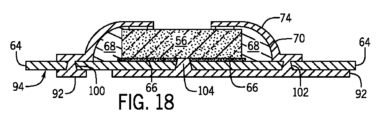
をさらに含む、請求項10に記載の方法。 - 電子機器パッケージであって、
絶縁基板の第1の表面に結合された裏面、前記絶縁基板とは反対側を向く活性表面、および前記活性表面と前記裏面との間に延びる複数の側壁を有する電気部品であって、前記活性表面は、撮像機能および光学機能の少なくとも一方を有する前記電気部品と、
前記複数の側壁によって形成される前記電気部品の周囲を封入し、その前記活性表面の一部を覆う絶縁構造であって、前記絶縁構造は前記電気部品と前記絶縁基板との間の領域には存在しない、絶縁構造と、
前記絶縁構造の傾斜側壁上に形成されて、前記電気部品の前記活性表面上の少なくとも1つの接触パッドに電気的に結合される第1の配線層と、
前記第1の表面に対向する前記絶縁基板の第2の表面に形成されて、前記絶縁基板に形成された少なくとも1つのビアを通って前記第1の配線層に電気的に結合された第2の配線層と、
前記絶縁構造および前記第1の配線層の少なくとも一部を取り囲む絶縁材料と、
を備え、
前記電気部品の前記活性表面の一部の上方の前記絶縁材料内に開口部が形成される、電子機器パッケージ。 - 前記電気部品の前記活性表面の上に配置された少なくとも1つのレンズをさらに備える、請求項15に記載の電子機器パッケージ。
- 前記第2の配線層は、前記絶縁基板に形成された別のビアを通って前記電気部品の前記裏面に結合される、請求項15に記載の電子機器パッケージ。
Applications Claiming Priority (3)
| Application Number | Priority Date | Filing Date | Title |
|---|---|---|---|
| US15/668,468 | 2017-08-03 | ||
| US15/668,468 US10541153B2 (en) | 2017-08-03 | 2017-08-03 | Electronics package with integrated interconnect structure and method of manufacturing thereof |
| PCT/US2018/043044 WO2019027698A1 (en) | 2017-08-03 | 2018-07-20 | ELECTRONIC HOUSING WITH INTEGRATED INTERCONNECTION STRUCTURE AND METHOD FOR MANUFACTURING THE SAME |
Publications (2)
| Publication Number | Publication Date |
|---|---|
| JP2020529734A JP2020529734A (ja) | 2020-10-08 |
| JP7343477B2 true JP7343477B2 (ja) | 2023-09-12 |
Family
ID=65229950
Family Applications (1)
| Application Number | Title | Priority Date | Filing Date |
|---|---|---|---|
| JP2020505444A Active JP7343477B2 (ja) | 2017-08-03 | 2018-07-20 | 統合相互接続構造を備えた電子機器パッケージおよびその製造方法 |
Country Status (6)
| Country | Link |
|---|---|
| US (2) | US10541153B2 (ja) |
| EP (1) | EP3662507A4 (ja) |
| JP (1) | JP7343477B2 (ja) |
| KR (1) | KR102622109B1 (ja) |
| CN (1) | CN110998828B (ja) |
| WO (1) | WO2019027698A1 (ja) |
Families Citing this family (11)
| Publication number | Priority date | Publication date | Assignee | Title |
|---|---|---|---|---|
| EP3355667A1 (de) * | 2017-01-30 | 2018-08-01 | Siemens Aktiengesellschaft | Verfahren zur herstellung einer elektrischen schaltung und elektrische schaltung |
| DE102017120168A1 (de) * | 2017-09-01 | 2019-03-07 | Osram Opto Semiconductors Gmbh | Verfahren zur Herstellung eines optoelektronischen Bauelements, optoelektronisches Bauelement und IR-Detektor |
| US10825782B2 (en) * | 2018-12-27 | 2020-11-03 | Micron Technology, Inc. | Semiconductor packages and associated methods with solder mask opening(s) for in-package ground and conformal coating contact |
| JP7402706B2 (ja) * | 2020-02-10 | 2023-12-21 | アオイ電子株式会社 | 発光装置の製造方法、および発光装置 |
| JP7502141B2 (ja) * | 2020-10-07 | 2024-06-18 | 伊東電機株式会社 | 発光素子モジュール、防爆照明器具、及び発光素子モジュールの製造方法 |
| US12230594B2 (en) * | 2020-12-31 | 2025-02-18 | Texas Instruments Incorporated | Printed package and method of making the same |
| US11829697B2 (en) * | 2021-08-06 | 2023-11-28 | International Business Machines Corporation | Region-based layout routing |
| US11935878B2 (en) * | 2021-09-10 | 2024-03-19 | Vanguard International Semiconductor Corporation | Package structure and method for manufacturing the same |
| US12034033B2 (en) | 2022-01-25 | 2024-07-09 | Ge Aviation Systems Llc | Semiconductor device package and method of forming |
| EP4465345A1 (en) * | 2023-05-17 | 2024-11-20 | Nexperia B.V. | Semiconductor device package interconnect and manufacturing method thereof |
| CN116435201B (zh) * | 2023-06-12 | 2023-09-12 | 四川遂宁市利普芯微电子有限公司 | 一种塑封封装方法以及器件封装结构 |
Citations (5)
| Publication number | Priority date | Publication date | Assignee | Title |
|---|---|---|---|---|
| US20040155322A1 (en) | 2003-02-07 | 2004-08-12 | Sung-Dae Cho | Semiconductor package with pattern leads and method for manufacturing the same |
| JP2004241493A (ja) | 2003-02-04 | 2004-08-26 | Kingpak Technology Inc | 位置ずれワイヤボンディング式イメージセンサ |
| JP2008205083A (ja) | 2007-02-19 | 2008-09-04 | Toshiba Corp | 半導体装置および取出し電極用ストラップ |
| JP2009076530A (ja) | 2007-09-19 | 2009-04-09 | Seiko Epson Corp | 配線パターンの形成方法 |
| JP2009200163A (ja) | 2008-02-20 | 2009-09-03 | Toyoda Gosei Co Ltd | Ledランプモジュール |
Family Cites Families (123)
| Publication number | Priority date | Publication date | Assignee | Title |
|---|---|---|---|---|
| JPH0951020A (ja) * | 1995-08-08 | 1997-02-18 | Hitachi Ltd | 半導体装置およびその製造方法ならびにicカード |
| US6284563B1 (en) | 1995-10-31 | 2001-09-04 | Tessera, Inc. | Method of making compliant microelectronic assemblies |
| JPH09254575A (ja) * | 1996-03-19 | 1997-09-30 | Denso Corp | 電子製品の製造方法 |
| JP3032964B2 (ja) * | 1996-12-30 | 2000-04-17 | アナムインダストリアル株式会社 | ボールグリッドアレイ半導体のパッケージ及び製造方法 |
| JPH10313071A (ja) * | 1997-05-09 | 1998-11-24 | Sony Corp | 電子部品及び配線基板装置 |
| US6306680B1 (en) | 1999-02-22 | 2001-10-23 | General Electric Company | Power overlay chip scale packages for discrete power devices |
| JP2001267473A (ja) * | 2000-03-17 | 2001-09-28 | Hitachi Ltd | 半導体装置およびその製造方法 |
| US6635971B2 (en) | 2001-01-11 | 2003-10-21 | Hitachi, Ltd. | Electronic device and optical transmission module |
| US7245500B2 (en) | 2002-02-01 | 2007-07-17 | Broadcom Corporation | Ball grid array package with stepped stiffener layer |
| US6861288B2 (en) | 2003-01-23 | 2005-03-01 | St Assembly Test Services, Ltd. | Stacked semiconductor packages and method for the fabrication thereof |
| JP3772984B2 (ja) | 2003-03-13 | 2006-05-10 | セイコーエプソン株式会社 | 電子装置及びその製造方法、回路基板並びに電子機器 |
| TWI233172B (en) | 2003-04-02 | 2005-05-21 | Siliconware Precision Industries Co Ltd | Non-leaded semiconductor package and method of fabricating the same |
| WO2005031861A1 (en) | 2003-09-26 | 2005-04-07 | Tessera, Inc. | Structure and method of making capped chips including a flowable conductive medium |
| US9029196B2 (en) | 2003-11-10 | 2015-05-12 | Stats Chippac, Ltd. | Semiconductor device and method of self-confinement of conductive bump material during reflow without solder mask |
| US7060601B2 (en) * | 2003-12-17 | 2006-06-13 | Tru-Si Technologies, Inc. | Packaging substrates for integrated circuits and soldering methods |
| JP4252019B2 (ja) * | 2004-09-01 | 2009-04-08 | 三洋電機株式会社 | 回路装置およびその製造方法 |
| JP4613590B2 (ja) * | 2004-11-16 | 2011-01-19 | セイコーエプソン株式会社 | 実装基板及び電子機器 |
| JP4400441B2 (ja) * | 2004-12-14 | 2010-01-20 | 三菱電機株式会社 | 半導体装置 |
| JPWO2006095834A1 (ja) | 2005-03-09 | 2008-08-21 | 旭化成エレクトロニクス株式会社 | 光デバイス及び光デバイスの製造方法 |
| TW200641969A (en) * | 2005-05-27 | 2006-12-01 | Siliconware Precision Industries Co Ltd | Sensor type semiconductor device and method for fabricating thereof |
| TWI251922B (en) * | 2005-07-14 | 2006-03-21 | Siliconware Precision Industries Co Ltd | Multichip stack structure |
| US7605476B2 (en) | 2005-09-27 | 2009-10-20 | Stmicroelectronics S.R.L. | Stacked die semiconductor package |
| US7902660B1 (en) * | 2006-05-24 | 2011-03-08 | Amkor Technology, Inc. | Substrate for semiconductor device and manufacturing method thereof |
| WO2007142052A1 (ja) | 2006-06-06 | 2007-12-13 | Nec Corporation | 半導体パッケージ、その製造方法、半導体装置、及び電子機器 |
| JP2008098478A (ja) * | 2006-10-13 | 2008-04-24 | Renesas Technology Corp | 半導体装置及びその製造方法 |
| KR100809718B1 (ko) | 2007-01-15 | 2008-03-06 | 삼성전자주식회사 | 이종 칩들을 갖는 적층형 반도체 칩 패키지 및 그 제조방법 |
| DE102007020656B4 (de) | 2007-04-30 | 2009-05-07 | Infineon Technologies Ag | Werkstück mit Halbleiterchips, Halbleiterbauteil und Verfahren zur Herstellung eines Werkstücks mit Halbleiterchips |
| US7750452B2 (en) | 2007-05-04 | 2010-07-06 | Stats Chippac, Ltd. | Same size die stacked package having through-hole vias formed in organic material |
| US7648858B2 (en) | 2007-06-19 | 2010-01-19 | Freescale Semiconductor, Inc. | Methods and apparatus for EMI shielding in multi-chip modules |
| JP4955488B2 (ja) * | 2007-09-05 | 2012-06-20 | 新光電気工業株式会社 | 半導体装置及びその製造方法 |
| US7651889B2 (en) | 2007-09-13 | 2010-01-26 | Freescale Semiconductor, Inc. | Electromagnetic shield formation for integrated circuit die package |
| US7777351B1 (en) * | 2007-10-01 | 2010-08-17 | Amkor Technology, Inc. | Thin stacked interposer package |
| JP5171288B2 (ja) | 2008-01-28 | 2013-03-27 | シャープ株式会社 | 固体撮像装置、固体撮像装置の実装方法、固体撮像装置の製造方法、および電子情報機器 |
| JP5690466B2 (ja) | 2008-01-31 | 2015-03-25 | インヴェンサス・コーポレイション | 半導体チップパッケージの製造方法 |
| US7752751B2 (en) | 2008-03-31 | 2010-07-13 | General Electric Company | System and method of forming a low profile conformal shield |
| JP2009246104A (ja) | 2008-03-31 | 2009-10-22 | Kyushu Institute Of Technology | 配線用電子部品及びその製造方法 |
| US8742558B2 (en) | 2008-05-21 | 2014-06-03 | General Electric Company | Component protection for advanced packaging applications |
| JP5345363B2 (ja) | 2008-06-24 | 2013-11-20 | シャープ株式会社 | 発光装置 |
| US20100073894A1 (en) * | 2008-09-22 | 2010-03-25 | Russell Mortensen | Coreless substrate, method of manufacturing same, and package for microelectronic device incorporating same |
| US8276268B2 (en) | 2008-11-03 | 2012-10-02 | General Electric Company | System and method of forming a patterned conformal structure |
| US8592992B2 (en) * | 2011-12-14 | 2013-11-26 | Stats Chippac, Ltd. | Semiconductor device and method of forming vertical interconnect structure with conductive micro via array for 3-D Fo-WLCSP |
| US8008125B2 (en) | 2009-03-06 | 2011-08-30 | General Electric Company | System and method for stacked die embedded chip build-up |
| US8358000B2 (en) | 2009-03-13 | 2013-01-22 | General Electric Company | Double side cooled power module with power overlay |
| US8097489B2 (en) | 2009-03-23 | 2012-01-17 | Stats Chippac, Ltd. | Semiconductor device and method of mounting pre-fabricated shielding frame over semiconductor die |
| US8115117B2 (en) | 2009-06-22 | 2012-02-14 | General Electric Company | System and method of forming isolated conformal shielding areas |
| US20110024899A1 (en) | 2009-07-28 | 2011-02-03 | Kenji Masumoto | Substrate structure for cavity package |
| US8263434B2 (en) | 2009-07-31 | 2012-09-11 | Stats Chippac, Ltd. | Semiconductor device and method of mounting die with TSV in cavity of substrate for electrical interconnect of Fi-PoP |
| US8183678B2 (en) * | 2009-08-04 | 2012-05-22 | Amkor Technology Korea, Inc. | Semiconductor device having an interposer |
| US8564133B2 (en) * | 2009-08-20 | 2013-10-22 | Ying-Nan Wen | Chip package and method for forming the same |
| JP5330184B2 (ja) * | 2009-10-06 | 2013-10-30 | 新光電気工業株式会社 | 電子部品装置 |
| US8630326B2 (en) | 2009-10-13 | 2014-01-14 | Skorpios Technologies, Inc. | Method and system of heterogeneous substrate bonding for photonic integration |
| US8319318B2 (en) | 2010-04-06 | 2012-11-27 | Intel Corporation | Forming metal filled die back-side film for electromagnetic interference shielding with coreless packages |
| US8531027B2 (en) | 2010-04-30 | 2013-09-10 | General Electric Company | Press-pack module with power overlay interconnection |
| US8946886B1 (en) * | 2010-05-13 | 2015-02-03 | Amkor Technology, Inc. | Shielded electronic component package and method |
| KR101855294B1 (ko) | 2010-06-10 | 2018-05-08 | 삼성전자주식회사 | 반도체 패키지 |
| US20110316140A1 (en) | 2010-06-29 | 2011-12-29 | Nalla Ravi K | Microelectronic package and method of manufacturing same |
| US8372666B2 (en) | 2010-07-06 | 2013-02-12 | Intel Corporation | Misalignment correction for embedded microelectronic die applications |
| TWI398943B (zh) * | 2010-08-25 | 2013-06-11 | Advanced Semiconductor Eng | 半導體封裝結構及其製程 |
| US9059187B2 (en) * | 2010-09-30 | 2015-06-16 | Ibiden Co., Ltd. | Electronic component having encapsulated wiring board and method for manufacturing the same |
| KR101711048B1 (ko) | 2010-10-07 | 2017-03-02 | 삼성전자 주식회사 | 차폐막을 포함하는 반도체 장치 및 제조 방법 |
| US20120112336A1 (en) | 2010-11-05 | 2012-05-10 | Guzek John S | Encapsulated die, microelectronic package containing same, and method of manufacturing said microelectronic package |
| JP2012114173A (ja) | 2010-11-23 | 2012-06-14 | Shinko Electric Ind Co Ltd | 半導体装置の製造方法及び半導体装置 |
| US20120139095A1 (en) | 2010-12-03 | 2012-06-07 | Manusharow Mathew J | Low-profile microelectronic package, method of manufacturing same, and electronic assembly containing same |
| US8508037B2 (en) | 2010-12-07 | 2013-08-13 | Intel Corporation | Bumpless build-up layer and laminated core hybrid structures and methods of assembling same |
| US20120146214A1 (en) | 2010-12-09 | 2012-06-14 | Mehdi Frederik Soltan | Semiconductor device with vias and flip-chip |
| KR101128063B1 (ko) * | 2011-05-03 | 2012-04-23 | 테세라, 인코포레이티드 | 캡슐화 층의 표면에 와이어 본드를 구비하는 패키지 적층형 어셈블리 |
| US8530277B2 (en) * | 2011-06-16 | 2013-09-10 | Stats Chippac Ltd. | Integrated circuit packaging system with package on package support and method of manufacture thereof |
| JP5837339B2 (ja) | 2011-06-20 | 2015-12-24 | 新光電気工業株式会社 | 半導体装置の製造方法及び半導体装置 |
| US8653635B2 (en) | 2011-08-16 | 2014-02-18 | General Electric Company | Power overlay structure with leadframe connections |
| KR101829392B1 (ko) | 2011-08-23 | 2018-02-20 | 삼성전자주식회사 | 반도체 패키지 및 그 제조 방법 |
| KR101800440B1 (ko) * | 2011-08-31 | 2017-11-23 | 삼성전자주식회사 | 다수의 반도체 칩들을 가진 반도체 패키지 및 그 형성 방법 |
| US8643148B2 (en) * | 2011-11-30 | 2014-02-04 | Taiwan Semiconductor Manufacturing Company, Ltd. | Chip-on-Wafer structures and methods for forming the same |
| US20130234317A1 (en) * | 2012-03-09 | 2013-09-12 | Taiwan Semiconductor Manufacturing Company, Ltd. | Packaging Methods and Packaged Semiconductor Devices |
| US8810024B2 (en) | 2012-03-23 | 2014-08-19 | Stats Chippac Ltd. | Semiconductor method and device of forming a fan-out PoP device with PWB vertical interconnect units |
| US9082780B2 (en) | 2012-03-23 | 2015-07-14 | Stats Chippac, Ltd. | Semiconductor device and method of forming a robust fan-out package including vertical interconnects and mechanical support layer |
| US9842798B2 (en) | 2012-03-23 | 2017-12-12 | STATS ChipPAC Pte. Ltd. | Semiconductor device and method of forming a PoP device with embedded vertical interconnect units |
| JP2013211407A (ja) * | 2012-03-30 | 2013-10-10 | J Devices:Kk | 半導体モジュール |
| US9548283B2 (en) | 2012-07-05 | 2017-01-17 | Taiwan Semiconductor Manufacturing Company, Ltd. | Package redistribution layer structure and method of forming same |
| US9299630B2 (en) | 2012-07-30 | 2016-03-29 | General Electric Company | Diffusion barrier for surface mount modules |
| US8941208B2 (en) | 2012-07-30 | 2015-01-27 | General Electric Company | Reliable surface mount integrated power module |
| US20140048951A1 (en) | 2012-08-14 | 2014-02-20 | Bridge Semiconductor Corporation | Semiconductor assembly with dual connecting channels between interposer and coreless substrate |
| US9443797B2 (en) | 2012-09-14 | 2016-09-13 | STATS ChipPAC Pte. Ltd. | Semiconductor device having wire studs as vertical interconnect in FO-WLP |
| KR101419597B1 (ko) * | 2012-11-06 | 2014-07-14 | 앰코 테크놀로지 코리아 주식회사 | 반도체 디바이스 및 그 제조 방법 |
| US9337163B2 (en) | 2012-11-13 | 2016-05-10 | General Electric Company | Low profile surface mount package with isolated tab |
| US9048222B2 (en) * | 2013-03-06 | 2015-06-02 | Taiwan Semiconductor Manufacturing Company, Ltd. | Method of fabricating interconnect structure for package-on-package devices |
| US8987876B2 (en) | 2013-03-14 | 2015-03-24 | General Electric Company | Power overlay structure and method of making same |
| US10269688B2 (en) | 2013-03-14 | 2019-04-23 | General Electric Company | Power overlay structure and method of making same |
| KR102226140B1 (ko) | 2013-03-15 | 2021-03-11 | 셀가드 엘엘씨 | 리튬 이온 이차 전지용 다층 하이브리드 전지 분리막 |
| KR20140126598A (ko) * | 2013-04-23 | 2014-10-31 | 삼성전자주식회사 | 반도체 패키지 및 그 제조 방법 |
| US8980691B2 (en) | 2013-06-28 | 2015-03-17 | Stats Chippac, Ltd. | Semiconductor device and method of forming low profile 3D fan-out package |
| US9368458B2 (en) * | 2013-07-10 | 2016-06-14 | Taiwan Semiconductor Manufacturing Company, Ltd. | Die-on-interposer assembly with dam structure and method of manufacturing the same |
| TW201438155A (zh) * | 2013-07-16 | 2014-10-01 | King Dragon Internat Inc | 具有傾斜結構之半導體元件封裝 |
| TWI525863B (zh) * | 2013-09-10 | 2016-03-11 | The wafer package structure is packaged using a wafer package structure A module, and a method of manufacturing the wafer package structure | |
| US9455211B2 (en) * | 2013-09-11 | 2016-09-27 | Taiwan Semiconductor Manufacturing Company, Ltd. | Integrated fan-out structure with openings in buffer layer |
| US9209151B2 (en) | 2013-09-26 | 2015-12-08 | General Electric Company | Embedded semiconductor device package and method of manufacturing thereof |
| KR20150042362A (ko) | 2013-10-10 | 2015-04-21 | 삼성전자주식회사 | 발광다이오드 패키지 및 그 제조방법 |
| US9209048B2 (en) * | 2013-12-30 | 2015-12-08 | Taiwan Semiconductor Manufacturing Company, Ltd. | Two step molding grinding for packaging applications |
| US9583411B2 (en) * | 2014-01-17 | 2017-02-28 | Invensas Corporation | Fine pitch BVA using reconstituted wafer with area array accessible for testing |
| US9583420B2 (en) * | 2015-01-23 | 2017-02-28 | Taiwan Semiconductor Manufacturing Company, Ltd. | Semiconductor device and method of manufactures |
| US9806051B2 (en) | 2014-03-04 | 2017-10-31 | General Electric Company | Ultra-thin embedded semiconductor device package and method of manufacturing thereof |
| US9281297B2 (en) * | 2014-03-07 | 2016-03-08 | Taiwan Semiconductor Manufacturing Company, Ltd. | Solution for reducing poor contact in info packages |
| US9735134B2 (en) | 2014-03-12 | 2017-08-15 | Taiwan Semiconductor Manufacturing Company, Ltd. | Packages with through-vias having tapered ends |
| US9627285B2 (en) | 2014-07-25 | 2017-04-18 | Dyi-chung Hu | Package substrate |
| US9496171B2 (en) * | 2014-09-26 | 2016-11-15 | Texas Instruments Incorporated | Printed interconnects for semiconductor packages |
| KR102165024B1 (ko) * | 2014-09-26 | 2020-10-13 | 인텔 코포레이션 | 와이어-접합 멀티-다이 스택을 구비한 집적 회로 패키지 |
| US9640521B2 (en) * | 2014-09-30 | 2017-05-02 | Taiwan Semiconductor Manufacturing Company, Ltd. | Multi-die package with bridge layer and method for making the same |
| US9613843B2 (en) | 2014-10-13 | 2017-04-04 | General Electric Company | Power overlay structure having wirebonds and method of manufacturing same |
| US9941207B2 (en) | 2014-10-24 | 2018-04-10 | STATS ChipPAC Pte. Ltd. | Semiconductor device and method of fabricating 3D package with short cycle time and high yield |
| US9812337B2 (en) | 2014-12-03 | 2017-11-07 | Taiwan Semiconductor Manufacturing Company, Ltd. | Integrated circuit package pad and methods of forming |
| US9548277B2 (en) * | 2015-04-21 | 2017-01-17 | Honeywell International Inc. | Integrated circuit stack including a patterned array of electrically conductive pillars |
| US9748212B2 (en) | 2015-04-30 | 2017-08-29 | Taiwan Semiconductor Manufacturing Company, Ltd. | Shadow pad for post-passivation interconnect structures |
| US9520385B1 (en) * | 2015-06-29 | 2016-12-13 | Taiwan Semiconductor Manufacturing Company, Ltd. | Package structure and method for forming same |
| US9786632B2 (en) * | 2015-07-30 | 2017-10-10 | Mediatek Inc. | Semiconductor package structure and method for forming the same |
| JP6569375B2 (ja) * | 2015-08-11 | 2019-09-04 | 株式会社ソシオネクスト | 半導体装置、半導体装置の製造方法及び電子装置 |
| KR101787832B1 (ko) | 2015-10-22 | 2017-10-19 | 앰코 테크놀로지 코리아 주식회사 | 반도체 패키지 제조 방법 및 이를 이용한 반도체 패키지 |
| US9786614B2 (en) * | 2015-11-16 | 2017-10-10 | Taiwan Semiconductor Manufacturing Company, Ltd. | Integrated fan-out structure and method of forming |
| KR101762627B1 (ko) * | 2015-11-17 | 2017-08-14 | 하나 마이크론(주) | 반도체 패키지 및 그 제조 방법 |
| CN106816431B (zh) * | 2015-11-30 | 2019-08-30 | 讯芯电子科技(中山)有限公司 | 一种电磁屏蔽封装结构及其制造方法 |
| KR102420125B1 (ko) * | 2015-12-10 | 2022-07-13 | 삼성전자주식회사 | 반도체 패키지 및 이의 제조방법 |
| US10351419B2 (en) * | 2016-05-20 | 2019-07-16 | Invensense, Inc. | Integrated package containing MEMS acoustic sensor and pressure sensor |
| US10276542B2 (en) * | 2016-07-21 | 2019-04-30 | Taiwan Semiconductor Manufacturing Co., Ltd. | Package structure and manufacturing method thereof |
| US10068879B2 (en) * | 2016-09-19 | 2018-09-04 | General Electric Company | Three-dimensional stacked integrated circuit devices and methods of assembling the same |
| US9953904B1 (en) * | 2016-10-25 | 2018-04-24 | Nxp Usa, Inc. | Electronic component package with heatsink and multiple electronic components |
-
2017
- 2017-08-03 US US15/668,468 patent/US10541153B2/en active Active
-
2018
- 2018-07-20 JP JP2020505444A patent/JP7343477B2/ja active Active
- 2018-07-20 CN CN201880050365.1A patent/CN110998828B/zh active Active
- 2018-07-20 EP EP18841174.8A patent/EP3662507A4/en active Pending
- 2018-07-20 KR KR1020207006027A patent/KR102622109B1/ko active Active
- 2018-07-20 WO PCT/US2018/043044 patent/WO2019027698A1/en unknown
-
2019
- 2019-10-29 US US16/667,018 patent/US10804116B2/en active Active
Patent Citations (5)
| Publication number | Priority date | Publication date | Assignee | Title |
|---|---|---|---|---|
| JP2004241493A (ja) | 2003-02-04 | 2004-08-26 | Kingpak Technology Inc | 位置ずれワイヤボンディング式イメージセンサ |
| US20040155322A1 (en) | 2003-02-07 | 2004-08-12 | Sung-Dae Cho | Semiconductor package with pattern leads and method for manufacturing the same |
| JP2008205083A (ja) | 2007-02-19 | 2008-09-04 | Toshiba Corp | 半導体装置および取出し電極用ストラップ |
| JP2009076530A (ja) | 2007-09-19 | 2009-04-09 | Seiko Epson Corp | 配線パターンの形成方法 |
| JP2009200163A (ja) | 2008-02-20 | 2009-09-03 | Toyoda Gosei Co Ltd | Ledランプモジュール |
Also Published As
| Publication number | Publication date |
|---|---|
| EP3662507A1 (en) | 2020-06-10 |
| EP3662507A4 (en) | 2021-09-29 |
| CN110998828B (zh) | 2021-04-13 |
| US20190043733A1 (en) | 2019-02-07 |
| KR20200028031A (ko) | 2020-03-13 |
| CN110998828A (zh) | 2020-04-10 |
| US20200066544A1 (en) | 2020-02-27 |
| KR102622109B1 (ko) | 2024-01-09 |
| JP2020529734A (ja) | 2020-10-08 |
| US10541153B2 (en) | 2020-01-21 |
| US10804116B2 (en) | 2020-10-13 |
| WO2019027698A1 (en) | 2019-02-07 |
Similar Documents
| Publication | Publication Date | Title |
|---|---|---|
| JP7343477B2 (ja) | 統合相互接続構造を備えた電子機器パッケージおよびその製造方法 | |
| US10497648B2 (en) | Embedded electronics package with multi-thickness interconnect structure and method of making same | |
| US10892231B2 (en) | Electronics package including integrated electromagnetic interference shield and method of manufacturing thereof | |
| US10804115B2 (en) | Electronics package with integrated interconnect structure and method of manufacturing thereof | |
| US20190043794A1 (en) | Electronics package including integrated structure with backside functionality and method of manufacturing thereof | |
| US10312194B2 (en) | Stacked electronics package and method of manufacturing thereof | |
| US10770444B2 (en) | Electronics package having a multi-thickness conductor layer and method of manufacturing thereof | |
| US10700035B2 (en) | Stacked electronics package and method of manufacturing thereof | |
| US20180130732A1 (en) | Electronics package having a multi-thickness conductor layer and method of manufacturing thereof | |
| US10553556B2 (en) | Electronics package having a multi-thickness conductor layer and method of manufacturing thereof | |
| US20180130731A1 (en) | Electronics package having a multi-thickness conductor layer and method of manufacturing thereof |
Legal Events
| Date | Code | Title | Description |
|---|---|---|---|
| A621 | Written request for application examination |
Free format text: JAPANESE INTERMEDIATE CODE: A621 Effective date: 20210622 |
|
| A977 | Report on retrieval |
Free format text: JAPANESE INTERMEDIATE CODE: A971007 Effective date: 20220523 |
|
| A131 | Notification of reasons for refusal |
Free format text: JAPANESE INTERMEDIATE CODE: A131 Effective date: 20220705 |
|
| A521 | Request for written amendment filed |
Free format text: JAPANESE INTERMEDIATE CODE: A523 Effective date: 20221004 |
|
| A131 | Notification of reasons for refusal |
Free format text: JAPANESE INTERMEDIATE CODE: A131 Effective date: 20230201 |
|
| A521 | Request for written amendment filed |
Free format text: JAPANESE INTERMEDIATE CODE: A523 Effective date: 20230424 |
|
| TRDD | Decision of grant or rejection written | ||
| A01 | Written decision to grant a patent or to grant a registration (utility model) |
Free format text: JAPANESE INTERMEDIATE CODE: A01 Effective date: 20230808 |
|
| A61 | First payment of annual fees (during grant procedure) |
Free format text: JAPANESE INTERMEDIATE CODE: A61 Effective date: 20230831 |
|
| R150 | Certificate of patent or registration of utility model |
Ref document number: 7343477 Country of ref document: JP Free format text: JAPANESE INTERMEDIATE CODE: R150 |