JP6268035B2 - 液晶表示装置及び電子機器 - Google Patents
液晶表示装置及び電子機器 Download PDFInfo
- Publication number
- JP6268035B2 JP6268035B2 JP2014098530A JP2014098530A JP6268035B2 JP 6268035 B2 JP6268035 B2 JP 6268035B2 JP 2014098530 A JP2014098530 A JP 2014098530A JP 2014098530 A JP2014098530 A JP 2014098530A JP 6268035 B2 JP6268035 B2 JP 6268035B2
- Authority
- JP
- Japan
- Prior art keywords
- liquid crystal
- crystal display
- substrate
- display device
- pixel
- Prior art date
- Legal status (The legal status is an assumption and is not a legal conclusion. Google has not performed a legal analysis and makes no representation as to the accuracy of the status listed.)
- Active
Links
- 239000004973 liquid crystal related substance Substances 0.000 title claims description 206
- 239000000758 substrate Substances 0.000 claims description 107
- 230000005684 electric field Effects 0.000 claims description 27
- 230000004044 response Effects 0.000 claims description 26
- 230000005540 biological transmission Effects 0.000 claims description 18
- 239000002861 polymer material Substances 0.000 claims description 7
- 229920000642 polymer Polymers 0.000 description 62
- 239000010408 film Substances 0.000 description 25
- 239000011159 matrix material Substances 0.000 description 21
- 238000010586 diagram Methods 0.000 description 17
- 238000011156 evaluation Methods 0.000 description 11
- 239000011521 glass Substances 0.000 description 10
- 238000000034 method Methods 0.000 description 10
- 239000004065 semiconductor Substances 0.000 description 10
- 230000006870 function Effects 0.000 description 9
- 239000010409 thin film Substances 0.000 description 9
- 229920001721 polyimide Polymers 0.000 description 5
- 239000004642 Polyimide Substances 0.000 description 4
- 239000003086 colorant Substances 0.000 description 4
- 239000000470 constituent Substances 0.000 description 4
- 229910052751 metal Inorganic materials 0.000 description 4
- 239000002184 metal Substances 0.000 description 4
- 239000000126 substance Substances 0.000 description 4
- 229910052782 aluminium Inorganic materials 0.000 description 3
- XAGFODPZIPBFFR-UHFFFAOYSA-N aluminium Chemical compound [Al] XAGFODPZIPBFFR-UHFFFAOYSA-N 0.000 description 3
- 239000003990 capacitor Substances 0.000 description 3
- 210000004027 cell Anatomy 0.000 description 3
- 239000011810 insulating material Substances 0.000 description 3
- 238000004873 anchoring Methods 0.000 description 2
- 238000004891 communication Methods 0.000 description 2
- 210000002858 crystal cell Anatomy 0.000 description 2
- 230000004927 fusion Effects 0.000 description 2
- 238000010030 laminating Methods 0.000 description 2
- 239000000463 material Substances 0.000 description 2
- 238000012986 modification Methods 0.000 description 2
- 230000004048 modification Effects 0.000 description 2
- 230000008569 process Effects 0.000 description 2
- 238000004088 simulation Methods 0.000 description 2
- ZOKXTWBITQBERF-UHFFFAOYSA-N Molybdenum Chemical compound [Mo] ZOKXTWBITQBERF-UHFFFAOYSA-N 0.000 description 1
- 229910052581 Si3N4 Inorganic materials 0.000 description 1
- 229910004205 SiNX Inorganic materials 0.000 description 1
- VYPSYNLAJGMNEJ-UHFFFAOYSA-N Silicium dioxide Chemical compound O=[Si]=O VYPSYNLAJGMNEJ-UHFFFAOYSA-N 0.000 description 1
- 238000010521 absorption reaction Methods 0.000 description 1
- 229910021417 amorphous silicon Inorganic materials 0.000 description 1
- 238000013459 approach Methods 0.000 description 1
- 230000000903 blocking effect Effects 0.000 description 1
- 239000004020 conductor Substances 0.000 description 1
- 238000001514 detection method Methods 0.000 description 1
- 230000006866 deterioration Effects 0.000 description 1
- 230000006872 improvement Effects 0.000 description 1
- AMGQUBHHOARCQH-UHFFFAOYSA-N indium;oxotin Chemical compound [In].[Sn]=O AMGQUBHHOARCQH-UHFFFAOYSA-N 0.000 description 1
- 238000009434 installation Methods 0.000 description 1
- 230000031700 light absorption Effects 0.000 description 1
- 229910044991 metal oxide Inorganic materials 0.000 description 1
- 150000004706 metal oxides Chemical class 0.000 description 1
- 229910052750 molybdenum Inorganic materials 0.000 description 1
- 239000011733 molybdenum Substances 0.000 description 1
- 230000002093 peripheral effect Effects 0.000 description 1
- 229910021420 polycrystalline silicon Inorganic materials 0.000 description 1
- 239000009719 polyimide resin Substances 0.000 description 1
- 229920005591 polysilicon Polymers 0.000 description 1
- 238000012545 processing Methods 0.000 description 1
- 239000011347 resin Substances 0.000 description 1
- 229920005989 resin Polymers 0.000 description 1
- HQVNEWCFYHHQES-UHFFFAOYSA-N silicon nitride Chemical compound N12[Si]34N5[Si]62N3[Si]51N64 HQVNEWCFYHHQES-UHFFFAOYSA-N 0.000 description 1
- 229910052814 silicon oxide Inorganic materials 0.000 description 1
- 238000006467 substitution reaction Methods 0.000 description 1
Images


Classifications
-
- G—PHYSICS
- G02—OPTICS
- G02F—OPTICAL DEVICES OR ARRANGEMENTS FOR THE CONTROL OF LIGHT BY MODIFICATION OF THE OPTICAL PROPERTIES OF THE MEDIA OF THE ELEMENTS INVOLVED THEREIN; NON-LINEAR OPTICS; FREQUENCY-CHANGING OF LIGHT; OPTICAL LOGIC ELEMENTS; OPTICAL ANALOGUE/DIGITAL CONVERTERS
- G02F1/00—Devices or arrangements for the control of the intensity, colour, phase, polarisation or direction of light arriving from an independent light source, e.g. switching, gating or modulating; Non-linear optics
- G02F1/01—Devices or arrangements for the control of the intensity, colour, phase, polarisation or direction of light arriving from an independent light source, e.g. switching, gating or modulating; Non-linear optics for the control of the intensity, phase, polarisation or colour
- G02F1/13—Devices or arrangements for the control of the intensity, colour, phase, polarisation or direction of light arriving from an independent light source, e.g. switching, gating or modulating; Non-linear optics for the control of the intensity, phase, polarisation or colour based on liquid crystals, e.g. single liquid crystal display cells
- G02F1/133—Constructional arrangements; Operation of liquid crystal cells; Circuit arrangements
- G02F1/1333—Constructional arrangements; Manufacturing methods
- G02F1/1343—Electrodes
- G02F1/134309—Electrodes characterised by their geometrical arrangement
-
- G—PHYSICS
- G02—OPTICS
- G02F—OPTICAL DEVICES OR ARRANGEMENTS FOR THE CONTROL OF LIGHT BY MODIFICATION OF THE OPTICAL PROPERTIES OF THE MEDIA OF THE ELEMENTS INVOLVED THEREIN; NON-LINEAR OPTICS; FREQUENCY-CHANGING OF LIGHT; OPTICAL LOGIC ELEMENTS; OPTICAL ANALOGUE/DIGITAL CONVERTERS
- G02F1/00—Devices or arrangements for the control of the intensity, colour, phase, polarisation or direction of light arriving from an independent light source, e.g. switching, gating or modulating; Non-linear optics
- G02F1/01—Devices or arrangements for the control of the intensity, colour, phase, polarisation or direction of light arriving from an independent light source, e.g. switching, gating or modulating; Non-linear optics for the control of the intensity, phase, polarisation or colour
- G02F1/13—Devices or arrangements for the control of the intensity, colour, phase, polarisation or direction of light arriving from an independent light source, e.g. switching, gating or modulating; Non-linear optics for the control of the intensity, phase, polarisation or colour based on liquid crystals, e.g. single liquid crystal display cells
- G02F1/133—Constructional arrangements; Operation of liquid crystal cells; Circuit arrangements
- G02F1/1333—Constructional arrangements; Manufacturing methods
- G02F1/133377—Cells with plural compartments or having plurality of liquid crystal microcells partitioned by walls, e.g. one microcell per pixel
-
- G—PHYSICS
- G02—OPTICS
- G02F—OPTICAL DEVICES OR ARRANGEMENTS FOR THE CONTROL OF LIGHT BY MODIFICATION OF THE OPTICAL PROPERTIES OF THE MEDIA OF THE ELEMENTS INVOLVED THEREIN; NON-LINEAR OPTICS; FREQUENCY-CHANGING OF LIGHT; OPTICAL LOGIC ELEMENTS; OPTICAL ANALOGUE/DIGITAL CONVERTERS
- G02F1/00—Devices or arrangements for the control of the intensity, colour, phase, polarisation or direction of light arriving from an independent light source, e.g. switching, gating or modulating; Non-linear optics
- G02F1/01—Devices or arrangements for the control of the intensity, colour, phase, polarisation or direction of light arriving from an independent light source, e.g. switching, gating or modulating; Non-linear optics for the control of the intensity, phase, polarisation or colour
- G02F1/13—Devices or arrangements for the control of the intensity, colour, phase, polarisation or direction of light arriving from an independent light source, e.g. switching, gating or modulating; Non-linear optics for the control of the intensity, phase, polarisation or colour based on liquid crystals, e.g. single liquid crystal display cells
- G02F1/133—Constructional arrangements; Operation of liquid crystal cells; Circuit arrangements
- G02F1/13306—Circuit arrangements or driving methods for the control of single liquid crystal cells
-
- G—PHYSICS
- G02—OPTICS
- G02F—OPTICAL DEVICES OR ARRANGEMENTS FOR THE CONTROL OF LIGHT BY MODIFICATION OF THE OPTICAL PROPERTIES OF THE MEDIA OF THE ELEMENTS INVOLVED THEREIN; NON-LINEAR OPTICS; FREQUENCY-CHANGING OF LIGHT; OPTICAL LOGIC ELEMENTS; OPTICAL ANALOGUE/DIGITAL CONVERTERS
- G02F1/00—Devices or arrangements for the control of the intensity, colour, phase, polarisation or direction of light arriving from an independent light source, e.g. switching, gating or modulating; Non-linear optics
- G02F1/01—Devices or arrangements for the control of the intensity, colour, phase, polarisation or direction of light arriving from an independent light source, e.g. switching, gating or modulating; Non-linear optics for the control of the intensity, phase, polarisation or colour
- G02F1/13—Devices or arrangements for the control of the intensity, colour, phase, polarisation or direction of light arriving from an independent light source, e.g. switching, gating or modulating; Non-linear optics for the control of the intensity, phase, polarisation or colour based on liquid crystals, e.g. single liquid crystal display cells
- G02F1/133—Constructional arrangements; Operation of liquid crystal cells; Circuit arrangements
- G02F1/1333—Constructional arrangements; Manufacturing methods
- G02F1/1334—Constructional arrangements; Manufacturing methods based on polymer dispersed liquid crystals, e.g. microencapsulated liquid crystals
-
- G—PHYSICS
- G02—OPTICS
- G02F—OPTICAL DEVICES OR ARRANGEMENTS FOR THE CONTROL OF LIGHT BY MODIFICATION OF THE OPTICAL PROPERTIES OF THE MEDIA OF THE ELEMENTS INVOLVED THEREIN; NON-LINEAR OPTICS; FREQUENCY-CHANGING OF LIGHT; OPTICAL LOGIC ELEMENTS; OPTICAL ANALOGUE/DIGITAL CONVERTERS
- G02F1/00—Devices or arrangements for the control of the intensity, colour, phase, polarisation or direction of light arriving from an independent light source, e.g. switching, gating or modulating; Non-linear optics
- G02F1/01—Devices or arrangements for the control of the intensity, colour, phase, polarisation or direction of light arriving from an independent light source, e.g. switching, gating or modulating; Non-linear optics for the control of the intensity, phase, polarisation or colour
- G02F1/13—Devices or arrangements for the control of the intensity, colour, phase, polarisation or direction of light arriving from an independent light source, e.g. switching, gating or modulating; Non-linear optics for the control of the intensity, phase, polarisation or colour based on liquid crystals, e.g. single liquid crystal display cells
- G02F1/133—Constructional arrangements; Operation of liquid crystal cells; Circuit arrangements
- G02F1/1333—Constructional arrangements; Manufacturing methods
- G02F1/1343—Electrodes
- G02F1/134309—Electrodes characterised by their geometrical arrangement
- G02F1/134336—Matrix
-
- G—PHYSICS
- G02—OPTICS
- G02F—OPTICAL DEVICES OR ARRANGEMENTS FOR THE CONTROL OF LIGHT BY MODIFICATION OF THE OPTICAL PROPERTIES OF THE MEDIA OF THE ELEMENTS INVOLVED THEREIN; NON-LINEAR OPTICS; FREQUENCY-CHANGING OF LIGHT; OPTICAL LOGIC ELEMENTS; OPTICAL ANALOGUE/DIGITAL CONVERTERS
- G02F1/00—Devices or arrangements for the control of the intensity, colour, phase, polarisation or direction of light arriving from an independent light source, e.g. switching, gating or modulating; Non-linear optics
- G02F1/01—Devices or arrangements for the control of the intensity, colour, phase, polarisation or direction of light arriving from an independent light source, e.g. switching, gating or modulating; Non-linear optics for the control of the intensity, phase, polarisation or colour
- G02F1/13—Devices or arrangements for the control of the intensity, colour, phase, polarisation or direction of light arriving from an independent light source, e.g. switching, gating or modulating; Non-linear optics for the control of the intensity, phase, polarisation or colour based on liquid crystals, e.g. single liquid crystal display cells
- G02F1/137—Devices or arrangements for the control of the intensity, colour, phase, polarisation or direction of light arriving from an independent light source, e.g. switching, gating or modulating; Non-linear optics for the control of the intensity, phase, polarisation or colour based on liquid crystals, e.g. single liquid crystal display cells characterised by the electro-optical or magneto-optical effect, e.g. field-induced phase transition, orientation effect, guest-host interaction or dynamic scattering
-
- G—PHYSICS
- G02—OPTICS
- G02F—OPTICAL DEVICES OR ARRANGEMENTS FOR THE CONTROL OF LIGHT BY MODIFICATION OF THE OPTICAL PROPERTIES OF THE MEDIA OF THE ELEMENTS INVOLVED THEREIN; NON-LINEAR OPTICS; FREQUENCY-CHANGING OF LIGHT; OPTICAL LOGIC ELEMENTS; OPTICAL ANALOGUE/DIGITAL CONVERTERS
- G02F1/00—Devices or arrangements for the control of the intensity, colour, phase, polarisation or direction of light arriving from an independent light source, e.g. switching, gating or modulating; Non-linear optics
- G02F1/01—Devices or arrangements for the control of the intensity, colour, phase, polarisation or direction of light arriving from an independent light source, e.g. switching, gating or modulating; Non-linear optics for the control of the intensity, phase, polarisation or colour
- G02F1/13—Devices or arrangements for the control of the intensity, colour, phase, polarisation or direction of light arriving from an independent light source, e.g. switching, gating or modulating; Non-linear optics for the control of the intensity, phase, polarisation or colour based on liquid crystals, e.g. single liquid crystal display cells
- G02F1/133—Constructional arrangements; Operation of liquid crystal cells; Circuit arrangements
- G02F1/1333—Constructional arrangements; Manufacturing methods
- G02F1/1335—Structural association of cells with optical devices, e.g. polarisers or reflectors
- G02F1/133509—Filters, e.g. light shielding masks
- G02F1/133512—Light shielding layers, e.g. black matrix
-
- G—PHYSICS
- G02—OPTICS
- G02F—OPTICAL DEVICES OR ARRANGEMENTS FOR THE CONTROL OF LIGHT BY MODIFICATION OF THE OPTICAL PROPERTIES OF THE MEDIA OF THE ELEMENTS INVOLVED THEREIN; NON-LINEAR OPTICS; FREQUENCY-CHANGING OF LIGHT; OPTICAL LOGIC ELEMENTS; OPTICAL ANALOGUE/DIGITAL CONVERTERS
- G02F1/00—Devices or arrangements for the control of the intensity, colour, phase, polarisation or direction of light arriving from an independent light source, e.g. switching, gating or modulating; Non-linear optics
- G02F1/01—Devices or arrangements for the control of the intensity, colour, phase, polarisation or direction of light arriving from an independent light source, e.g. switching, gating or modulating; Non-linear optics for the control of the intensity, phase, polarisation or colour
- G02F1/13—Devices or arrangements for the control of the intensity, colour, phase, polarisation or direction of light arriving from an independent light source, e.g. switching, gating or modulating; Non-linear optics for the control of the intensity, phase, polarisation or colour based on liquid crystals, e.g. single liquid crystal display cells
- G02F1/133—Constructional arrangements; Operation of liquid crystal cells; Circuit arrangements
- G02F1/1333—Constructional arrangements; Manufacturing methods
- G02F1/1343—Electrodes
- G02F1/134309—Electrodes characterised by their geometrical arrangement
- G02F1/134372—Electrodes characterised by their geometrical arrangement for fringe field switching [FFS] where the common electrode is not patterned
-
- G—PHYSICS
- G02—OPTICS
- G02F—OPTICAL DEVICES OR ARRANGEMENTS FOR THE CONTROL OF LIGHT BY MODIFICATION OF THE OPTICAL PROPERTIES OF THE MEDIA OF THE ELEMENTS INVOLVED THEREIN; NON-LINEAR OPTICS; FREQUENCY-CHANGING OF LIGHT; OPTICAL LOGIC ELEMENTS; OPTICAL ANALOGUE/DIGITAL CONVERTERS
- G02F1/00—Devices or arrangements for the control of the intensity, colour, phase, polarisation or direction of light arriving from an independent light source, e.g. switching, gating or modulating; Non-linear optics
- G02F1/01—Devices or arrangements for the control of the intensity, colour, phase, polarisation or direction of light arriving from an independent light source, e.g. switching, gating or modulating; Non-linear optics for the control of the intensity, phase, polarisation or colour
- G02F1/13—Devices or arrangements for the control of the intensity, colour, phase, polarisation or direction of light arriving from an independent light source, e.g. switching, gating or modulating; Non-linear optics for the control of the intensity, phase, polarisation or colour based on liquid crystals, e.g. single liquid crystal display cells
- G02F1/133—Constructional arrangements; Operation of liquid crystal cells; Circuit arrangements
- G02F1/1333—Constructional arrangements; Manufacturing methods
- G02F1/1343—Electrodes
- G02F1/134309—Electrodes characterised by their geometrical arrangement
- G02F1/134381—Hybrid switching mode, i.e. for applying an electric field with components parallel and orthogonal to the substrates
Landscapes
- Physics & Mathematics (AREA)
- Nonlinear Science (AREA)
- Chemical & Material Sciences (AREA)
- Crystallography & Structural Chemistry (AREA)
- General Physics & Mathematics (AREA)
- Optics & Photonics (AREA)
- Mathematical Physics (AREA)
- Geometry (AREA)
- Liquid Crystal (AREA)
- Dispersion Chemistry (AREA)
Description
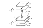
図1は、本実施形態に係る液晶表示装置の一例を表す説明図である。図2は、図1の液晶表示装置のシステム例を表すブロック図である。図1は模式的に表したものであり、実際の寸法、形状と同一とは限らない。なお、表示装置1が本発明の「液晶表示装置」の一具体例に相当する。
画素基板60は、透光性基板71に各種回路が形成されたTFT基板であり、この画素基板60上にマトリクス状に配設された複数の画素電極72と、共通電極comと、を含む。図6に示すように、画素電極72と共通電極comとは、絶縁層74で絶縁され、画素基板60の表面に垂直な方向において、対向している。画素電極72及び共通電極comは、ITO(Indium Tin Oxide)等の透光性導電材料(透光性導電酸化物)で形成される透光性電極である。
図16は、実施形態2に係る液晶表示部の画素と高分子壁との位置関係を説明するための平面模式図である。上述した実施形態で説明したものと同じ構成要素には同一の符号を付して重複する説明は省略する。
図17は、実施形態3に係る液晶表示部の遮光部を説明するための断面模式図である。上述した実施形態で説明したものと同じ構成要素には同一の符号を付して重複する説明は省略する。
評価例1乃至評価例3について、以下、評価した結果を説明する。これら評価例で、本発明は限定されるものではない。図18は、実施形態1に係る液晶表示部の評価例1において、画素の応答速度と高分子壁との関係を説明するための説明図である。隣り合う高分子壁55間の平均間隔lが無限大の電圧OFF時の基準応答時間Tfを1として、評価例1の副画素Vpixの開口幅、セル厚d、高分子壁55の幅wを同一の条件とした場合における平均間隔lが2μm、3μm、5μm、10μm、20μm、100μmの基準応答時間に対する電圧OFF時応答時間τの相対値をシミュレーションした。図18は、シミュレーション結果を示している。図18に示すように、平均間隔lが10μm以下の場合、液晶表示装置1は、電圧OFF時応答時間τを早くすることができる。その結果、表示装置1は、液晶の応答速度を早くすることができる。
次に、図20及び図21を参照して、実施形態1から実施形態3で説明した表示装置1の適用例について説明する。図20及び図21は、本実施形態に係る液晶表示装置を適用する電子機器の一例を示す図である。本実施形態に係る表示装置1は、図20に示すカーナビゲーションシステム、テレビジョン装置、デジタルカメラ、ノート型パーソナルコンピュータ、図21に示す携帯電話等の携帯端末装置あるいはビデオカメラなどのあらゆる分野の電子機器に適用することが可能である。言い換えると、本実施形態に係る表示装置1は、外部から入力された映像信号あるいは内部で生成した映像信号を、画像あるいは映像として表示するあらゆる分野の電子機器に適用することが可能である。電子機器は、液晶表示装置に映像信号を供給し、液晶表示装置の動作を制御する制御装置4(図2参照)を備える。
2 液晶表示部
4 制御装置
6 バックライト
11 ガラス基板
21 表示エリア部
54 液晶層
55、56 高分子壁
60 画素基板
64 対向基板
66 カラーフィルタ
72 画素電極(第1電極)
74 絶縁層
76a ブラックマトリクス
76b 開口部
90 半導体層
BM1、BM2 遮光部
com 共通電極(第2電極)
Vpix 副画素
Claims (10)
- 第1基板と、
前記第1基板に対向配置された第2基板と、
前記第1基板と前記第2基板との間に配置される液晶分子を含む液晶層と、
第1方向に延在する走査線と、
第2方向に延在する信号線と、
隣接する2本の走査線と隣接する2本の信号線で囲われた画素領域と、
画素領域毎に配置される第1電極と、
前記第1電極と対向する位置に配置された第2電極と、
前記第1方向に延在し、前記第2方向に配列される前記液晶分子の回転が抑制された複数の無透過領域を有し、
前記無透過領域に挟まれて、前記第1電極と前記第2電極との間で作用する電界に応じて前記液晶分子が回転する透過領域と、を有し、
隣接する2つの画素領域において、複数の前記無透過領域の第2方向の配置位置は、同一であって、
1つの画素領域に含まれる前記無透過領域間の第2方向における平均間隔は10μm以下である、
液晶表示装置。 - 前記画素領域において、無透過領域は、前記第1方向に延びる複数の第1部分領域と、前記複数の第1部分領域と交差する第2方向に延在する少なくとも1つの第2部分領域を有する、
請求項1に記載の液晶表示装置。 - 前記画素領域において、前記第2部分領域は複数配置され、第1部分領域と第2部分領域で格子状に形成される、
請求項2に記載の液晶表示装置。 - 前記画素領域において、前記第2部分領域は複数配置され、前記第2部分領域間の距離は10μm以下である、
請求項2に記載の液晶表示装置。 - 前記第1方向は、電圧無印加時の液晶分子の配向方向である、
請求項1乃至4のいずれか1項に記載の液晶表示装置。 - 前記無透過領域には、前記液晶分子と、前記液晶分子を囲む高分子材料とを含み、前記高分子材料は、前記第1基板及び前記第2基板の一方から他方へ立設する高分子壁となっている、請求項1又は5に記載の液晶表示装置。
- 遮光部をさらに備え、前記第1基板の垂直方向において、前記第1基板又は前記第2基板の、前記無透過領域と重なる領域に配置されている、請求項1乃至6のいずれか1項に記載の液晶表示装置。
- 前記遮光部は、前記画素を囲う遮光部と接続している、請求項7に記載の液晶表示装置。
- 前記遮光部は、前記第1電極又は前記第2電極を作用させる配線である、請求項7に記載の液晶表示装置。
- 請求項1乃至9のいずれか1項に記載の液晶表示装置と、前記液晶表示装置に映像信号を供給し、前記液晶表示装置の動作を制御する制御装置とを備える、電子機器。
Priority Applications (4)
| Application Number | Priority Date | Filing Date | Title |
|---|---|---|---|
| JP2014098530A JP6268035B2 (ja) | 2014-05-12 | 2014-05-12 | 液晶表示装置及び電子機器 |
| CN201510232309.8A CN105093597B (zh) | 2014-05-12 | 2015-05-08 | 液晶显示装置及电子设备 |
| US14/707,171 US9891456B2 (en) | 2014-05-12 | 2015-05-08 | Liquid crystal display device and electronic apparatus |
| US15/861,918 US10371978B2 (en) | 2014-05-12 | 2018-01-04 | Liquid crystal display device and electronic apparatus |
Applications Claiming Priority (1)
| Application Number | Priority Date | Filing Date | Title |
|---|---|---|---|
| JP2014098530A JP6268035B2 (ja) | 2014-05-12 | 2014-05-12 | 液晶表示装置及び電子機器 |
Publications (2)
| Publication Number | Publication Date |
|---|---|
| JP2015215492A JP2015215492A (ja) | 2015-12-03 |
| JP6268035B2 true JP6268035B2 (ja) | 2018-01-24 |
Family
ID=54367755
Family Applications (1)
| Application Number | Title | Priority Date | Filing Date |
|---|---|---|---|
| JP2014098530A Active JP6268035B2 (ja) | 2014-05-12 | 2014-05-12 | 液晶表示装置及び電子機器 |
Country Status (3)
| Country | Link |
|---|---|
| US (2) | US9891456B2 (ja) |
| JP (1) | JP6268035B2 (ja) |
| CN (1) | CN105093597B (ja) |
Families Citing this family (6)
| Publication number | Priority date | Publication date | Assignee | Title |
|---|---|---|---|---|
| WO2019060033A1 (en) * | 2017-09-21 | 2019-03-28 | Apple Inc. | LIQUID CRYSTAL DISPLAY |
| JP7083102B2 (ja) * | 2017-11-29 | 2022-06-10 | Tianma Japan株式会社 | 光線方向制御デバイス及び表示装置 |
| JP7109957B2 (ja) * | 2018-03-27 | 2022-08-01 | 株式会社ジャパンディスプレイ | 表示装置 |
| JP7118722B2 (ja) | 2018-04-25 | 2022-08-16 | 株式会社ジャパンディスプレイ | 液晶表示装置 |
| CN108957814B (zh) * | 2018-08-29 | 2021-08-13 | 南京京东方显示技术有限公司 | 一种液晶显示装置及电路补偿方法 |
| JP2020160322A (ja) * | 2019-03-27 | 2020-10-01 | 株式会社ジャパンディスプレイ | 表示装置 |
Family Cites Families (27)
| Publication number | Priority date | Publication date | Assignee | Title |
|---|---|---|---|---|
| US5148302A (en) * | 1986-04-10 | 1992-09-15 | Akihiko Nagano | Optical modulation element having two-dimensional phase type diffraction grating |
| JP2937684B2 (ja) | 1992-11-30 | 1999-08-23 | シャープ株式会社 | 液晶表示素子及びその製造方法 |
| US5579140A (en) * | 1993-04-22 | 1996-11-26 | Sharp Kabushiki Kaisha | Multiple domain liquid crystal display element and a manufacturing method of the same |
| JP2933816B2 (ja) * | 1993-07-15 | 1999-08-16 | シャープ株式会社 | 液晶表示素子及びその製造方法 |
| US5668651A (en) * | 1994-03-18 | 1997-09-16 | Sharp Kabushiki Kaisha | Polymer-wall LCD having liquid crystal molecules having a plane-symmetrical bend orientation |
| JP2002244137A (ja) * | 2001-02-13 | 2002-08-28 | Matsushita Electric Ind Co Ltd | 液晶表示パネルおよび画像表示応用機器 |
| JP3875125B2 (ja) * | 2001-04-11 | 2007-01-31 | シャープ株式会社 | 液晶表示装置 |
| US6924870B1 (en) * | 2002-04-30 | 2005-08-02 | Kent State University | Liquid crystal on silicon diffractive light valve |
| KR100951348B1 (ko) * | 2003-04-04 | 2010-04-08 | 삼성전자주식회사 | 다중 도메인 액정 표시 장치 및 그 박막 트랜지스터 기판 |
| JP4684808B2 (ja) * | 2005-08-29 | 2011-05-18 | 株式会社 日立ディスプレイズ | 液晶表示装置及びそれを備えた情報端末機器 |
| KR101229053B1 (ko) * | 2006-05-15 | 2013-02-04 | 엘지디스플레이 주식회사 | 액정 표시 장치 및 그의 제조 방법 |
| JP2008039910A (ja) * | 2006-08-02 | 2008-02-21 | Hitachi Displays Ltd | 液晶表示装置 |
| JP2008052161A (ja) | 2006-08-28 | 2008-03-06 | Epson Imaging Devices Corp | 液晶装置及び電子機器 |
| WO2009069249A1 (ja) | 2007-11-30 | 2009-06-04 | Sharp Kabushiki Kaisha | 液晶表示装置 |
| JP2010008842A (ja) * | 2008-06-30 | 2010-01-14 | Seiko Epson Corp | 液晶装置、液晶装置の製造方法、及び電子機器 |
| WO2010044246A1 (ja) * | 2008-10-15 | 2010-04-22 | シャープ株式会社 | 液晶表示装置およびその製造方法 |
| KR101742529B1 (ko) * | 2010-12-23 | 2017-06-16 | 삼성디스플레이 주식회사 | 액정 표시 장치 및 액정 표시 장치의 제조 방법 |
| US20140168581A1 (en) * | 2011-08-02 | 2014-06-19 | Sharp Kabushiki Kaisha | Lcd panel, electronic device, and method for producing lcd panel |
| JP5937389B2 (ja) | 2011-10-25 | 2016-06-22 | 株式会社ジャパンディスプレイ | 表示装置、電子機器、および、表示装置の製造方法 |
| JP5767186B2 (ja) | 2012-09-28 | 2015-08-19 | 株式会社ジャパンディスプレイ | 表示装置及び電子機器 |
| US9746706B2 (en) | 2012-10-26 | 2017-08-29 | Japan Display Inc. | Display device and electronic apparatus |
| JP2014209228A (ja) | 2013-03-29 | 2014-11-06 | 株式会社ジャパンディスプレイ | 液晶表示装置及び電子機器 |
| JP2014209213A (ja) | 2013-03-29 | 2014-11-06 | 株式会社ジャパンディスプレイ | 液晶表示装置及び電子機器 |
| JP2014209212A (ja) | 2013-03-29 | 2014-11-06 | 株式会社ジャパンディスプレイ | 液晶表示装置及び電子機器 |
| JP2014206639A (ja) | 2013-04-12 | 2014-10-30 | 株式会社ジャパンディスプレイ | 液晶表示装置 |
| JP2014215444A (ja) | 2013-04-25 | 2014-11-17 | 株式会社ジャパンディスプレイ | 液晶表示装置 |
| JP6014552B2 (ja) | 2013-05-28 | 2016-10-25 | 株式会社ジャパンディスプレイ | 表示装置及び電子機器 |
-
2014
- 2014-05-12 JP JP2014098530A patent/JP6268035B2/ja active Active
-
2015
- 2015-05-08 US US14/707,171 patent/US9891456B2/en active Active
- 2015-05-08 CN CN201510232309.8A patent/CN105093597B/zh active Active
-
2018
- 2018-01-04 US US15/861,918 patent/US10371978B2/en active Active
Also Published As
| Publication number | Publication date |
|---|---|
| US10371978B2 (en) | 2019-08-06 |
| US20150323841A1 (en) | 2015-11-12 |
| CN105093597B (zh) | 2018-06-26 |
| US9891456B2 (en) | 2018-02-13 |
| JP2015215492A (ja) | 2015-12-03 |
| US20180129097A1 (en) | 2018-05-10 |
| CN105093597A (zh) | 2015-11-25 |
Similar Documents
| Publication | Publication Date | Title |
|---|---|---|
| US11754897B2 (en) | Liquid crystal display | |
| US10371978B2 (en) | Liquid crystal display device and electronic apparatus | |
| US9377658B2 (en) | Liquid crystal display device and electronic apparatus | |
| US10578932B2 (en) | Liquid crystal display device and electronic apparatus | |
| US9188824B2 (en) | Display device | |
| JP2016029475A (ja) | 液晶表示装置及び電子機器 | |
| US20140146094A1 (en) | Display device and electronic apparatus | |
| US9857613B2 (en) | Liquid crystal display device and electronic apparatus | |
| JP2014149322A (ja) | 液晶表示パネル及び電子機器 | |
| JP6630068B2 (ja) | 液晶表示装置 | |
| JP2015118189A (ja) | 液晶表示装置及び電子機器 | |
| JP2016051145A (ja) | 液晶表示装置及び電子機器 | |
| JP2014178629A (ja) | 液晶表示パネル及び電子機器 | |
| JP6326518B2 (ja) | 液晶表示装置 | |
| JP2014235420A (ja) | 液晶表示パネル、電子機器及び画素基板製造方法 |
Legal Events
| Date | Code | Title | Description |
|---|---|---|---|
| A621 | Written request for application examination |
Free format text: JAPANESE INTERMEDIATE CODE: A621 Effective date: 20161128 |
|
| A131 | Notification of reasons for refusal |
Free format text: JAPANESE INTERMEDIATE CODE: A131 Effective date: 20170815 |
|
| A977 | Report on retrieval |
Free format text: JAPANESE INTERMEDIATE CODE: A971007 Effective date: 20170816 |
|
| A521 | Request for written amendment filed |
Free format text: JAPANESE INTERMEDIATE CODE: A523 Effective date: 20171011 |
|
| A131 | Notification of reasons for refusal |
Free format text: JAPANESE INTERMEDIATE CODE: A131 Effective date: 20171031 |
|
| A521 | Request for written amendment filed |
Free format text: JAPANESE INTERMEDIATE CODE: A523 Effective date: 20171128 |
|
| TRDD | Decision of grant or rejection written | ||
| A01 | Written decision to grant a patent or to grant a registration (utility model) |
Free format text: JAPANESE INTERMEDIATE CODE: A01 Effective date: 20171205 |
|
| R150 | Certificate of patent or registration of utility model |
Ref document number: 6268035 Country of ref document: JP Free format text: JAPANESE INTERMEDIATE CODE: R150 |
|
| R250 | Receipt of annual fees |
Free format text: JAPANESE INTERMEDIATE CODE: R250 |
|
| R250 | Receipt of annual fees |
Free format text: JAPANESE INTERMEDIATE CODE: R250 |
|
| R250 | Receipt of annual fees |
Free format text: JAPANESE INTERMEDIATE CODE: R250 |
|
| R250 | Receipt of annual fees |
Free format text: JAPANESE INTERMEDIATE CODE: R250 |
|
| R250 | Receipt of annual fees |
Free format text: JAPANESE INTERMEDIATE CODE: R250 |