EP1168430B1 - Semiconductor device and method of manufacturing the same - Google Patents
Semiconductor device and method of manufacturing the same Download PDFInfo
- Publication number
- EP1168430B1 EP1168430B1 EP00128270A EP00128270A EP1168430B1 EP 1168430 B1 EP1168430 B1 EP 1168430B1 EP 00128270 A EP00128270 A EP 00128270A EP 00128270 A EP00128270 A EP 00128270A EP 1168430 B1 EP1168430 B1 EP 1168430B1
- Authority
- EP
- European Patent Office
- Prior art keywords
- region
- insulating film
- semiconductor layer
- semiconductor
- film
- Prior art date
- Legal status (The legal status is an assumption and is not a legal conclusion. Google has not performed a legal analysis and makes no representation as to the accuracy of the status listed.)
- Expired - Lifetime
Links
Images


Classifications
-
- H—ELECTRICITY
- H01—ELECTRIC ELEMENTS
- H01L—SEMICONDUCTOR DEVICES NOT COVERED BY CLASS H10
- H01L21/00—Processes or apparatus adapted for the manufacture or treatment of semiconductor or solid state devices or of parts thereof
- H01L21/70—Manufacture or treatment of devices consisting of a plurality of solid state components formed in or on a common substrate or of parts thereof; Manufacture of integrated circuit devices or of parts thereof
- H01L21/71—Manufacture of specific parts of devices defined in group H01L21/70
- H01L21/76—Making of isolation regions between components
- H01L21/762—Dielectric regions, e.g. EPIC dielectric isolation, LOCOS; Trench refilling techniques, SOI technology, use of channel stoppers
- H01L21/7624—Dielectric regions, e.g. EPIC dielectric isolation, LOCOS; Trench refilling techniques, SOI technology, use of channel stoppers using semiconductor on insulator [SOI] technology
- H01L21/76264—SOI together with lateral isolation, e.g. using local oxidation of silicon, or dielectric or polycristalline material refilled trench or air gap isolation regions, e.g. completely isolated semiconductor islands
-
- H—ELECTRICITY
- H10—SEMICONDUCTOR DEVICES; ELECTRIC SOLID-STATE DEVICES NOT OTHERWISE PROVIDED FOR
- H10D—INORGANIC ELECTRIC SEMICONDUCTOR DEVICES
- H10D86/00—Integrated devices formed in or on insulating or conducting substrates, e.g. formed in silicon-on-insulator [SOI] substrates or on stainless steel or glass substrates
- H10D86/01—Manufacture or treatment
-
- H—ELECTRICITY
- H01—ELECTRIC ELEMENTS
- H01L—SEMICONDUCTOR DEVICES NOT COVERED BY CLASS H10
- H01L21/00—Processes or apparatus adapted for the manufacture or treatment of semiconductor or solid state devices or of parts thereof
- H01L21/02—Manufacture or treatment of semiconductor devices or of parts thereof
- H01L21/02104—Forming layers
- H01L21/02107—Forming insulating materials on a substrate
- H01L21/02109—Forming insulating materials on a substrate characterised by the type of layer, e.g. type of material, porous/non-porous, pre-cursors, mixtures or laminates
- H01L21/02112—Forming insulating materials on a substrate characterised by the type of layer, e.g. type of material, porous/non-porous, pre-cursors, mixtures or laminates characterised by the material of the layer
- H01L21/02123—Forming insulating materials on a substrate characterised by the type of layer, e.g. type of material, porous/non-porous, pre-cursors, mixtures or laminates characterised by the material of the layer the material containing silicon
- H01L21/02126—Forming insulating materials on a substrate characterised by the type of layer, e.g. type of material, porous/non-porous, pre-cursors, mixtures or laminates characterised by the material of the layer the material containing silicon the material containing Si, O, and at least one of H, N, C, F, or other non-metal elements, e.g. SiOC, SiOC:H or SiONC
- H01L21/02129—Forming insulating materials on a substrate characterised by the type of layer, e.g. type of material, porous/non-porous, pre-cursors, mixtures or laminates characterised by the material of the layer the material containing silicon the material containing Si, O, and at least one of H, N, C, F, or other non-metal elements, e.g. SiOC, SiOC:H or SiONC the material being boron or phosphorus doped silicon oxides, e.g. BPSG, BSG or PSG
-
- H—ELECTRICITY
- H01—ELECTRIC ELEMENTS
- H01L—SEMICONDUCTOR DEVICES NOT COVERED BY CLASS H10
- H01L21/00—Processes or apparatus adapted for the manufacture or treatment of semiconductor or solid state devices or of parts thereof
- H01L21/02—Manufacture or treatment of semiconductor devices or of parts thereof
- H01L21/02104—Forming layers
- H01L21/02107—Forming insulating materials on a substrate
- H01L21/02109—Forming insulating materials on a substrate characterised by the type of layer, e.g. type of material, porous/non-porous, pre-cursors, mixtures or laminates
- H01L21/02112—Forming insulating materials on a substrate characterised by the type of layer, e.g. type of material, porous/non-porous, pre-cursors, mixtures or laminates characterised by the material of the layer
- H01L21/02123—Forming insulating materials on a substrate characterised by the type of layer, e.g. type of material, porous/non-porous, pre-cursors, mixtures or laminates characterised by the material of the layer the material containing silicon
- H01L21/02164—Forming insulating materials on a substrate characterised by the type of layer, e.g. type of material, porous/non-porous, pre-cursors, mixtures or laminates characterised by the material of the layer the material containing silicon the material being a silicon oxide, e.g. SiO2
-
- H—ELECTRICITY
- H01—ELECTRIC ELEMENTS
- H01L—SEMICONDUCTOR DEVICES NOT COVERED BY CLASS H10
- H01L21/00—Processes or apparatus adapted for the manufacture or treatment of semiconductor or solid state devices or of parts thereof
- H01L21/02—Manufacture or treatment of semiconductor devices or of parts thereof
- H01L21/02104—Forming layers
- H01L21/02107—Forming insulating materials on a substrate
- H01L21/02109—Forming insulating materials on a substrate characterised by the type of layer, e.g. type of material, porous/non-porous, pre-cursors, mixtures or laminates
- H01L21/02112—Forming insulating materials on a substrate characterised by the type of layer, e.g. type of material, porous/non-porous, pre-cursors, mixtures or laminates characterised by the material of the layer
- H01L21/02123—Forming insulating materials on a substrate characterised by the type of layer, e.g. type of material, porous/non-porous, pre-cursors, mixtures or laminates characterised by the material of the layer the material containing silicon
- H01L21/0217—Forming insulating materials on a substrate characterised by the type of layer, e.g. type of material, porous/non-porous, pre-cursors, mixtures or laminates characterised by the material of the layer the material containing silicon the material being a silicon nitride not containing oxygen, e.g. SixNy or SixByNz
-
- H—ELECTRICITY
- H01—ELECTRIC ELEMENTS
- H01L—SEMICONDUCTOR DEVICES NOT COVERED BY CLASS H10
- H01L21/00—Processes or apparatus adapted for the manufacture or treatment of semiconductor or solid state devices or of parts thereof
- H01L21/02—Manufacture or treatment of semiconductor devices or of parts thereof
- H01L21/02104—Forming layers
- H01L21/02107—Forming insulating materials on a substrate
- H01L21/02109—Forming insulating materials on a substrate characterised by the type of layer, e.g. type of material, porous/non-porous, pre-cursors, mixtures or laminates
- H01L21/022—Forming insulating materials on a substrate characterised by the type of layer, e.g. type of material, porous/non-porous, pre-cursors, mixtures or laminates the layer being a laminate, i.e. composed of sublayers, e.g. stacks of alternating high-k metal oxides
-
- H—ELECTRICITY
- H01—ELECTRIC ELEMENTS
- H01L—SEMICONDUCTOR DEVICES NOT COVERED BY CLASS H10
- H01L21/00—Processes or apparatus adapted for the manufacture or treatment of semiconductor or solid state devices or of parts thereof
- H01L21/02—Manufacture or treatment of semiconductor devices or of parts thereof
- H01L21/02104—Forming layers
- H01L21/02107—Forming insulating materials on a substrate
- H01L21/02225—Forming insulating materials on a substrate characterised by the process for the formation of the insulating layer
- H01L21/0226—Forming insulating materials on a substrate characterised by the process for the formation of the insulating layer formation by a deposition process
- H01L21/02263—Forming insulating materials on a substrate characterised by the process for the formation of the insulating layer formation by a deposition process deposition from the gas or vapour phase
- H01L21/02271—Forming insulating materials on a substrate characterised by the process for the formation of the insulating layer formation by a deposition process deposition from the gas or vapour phase deposition by decomposition or reaction of gaseous or vapour phase compounds, i.e. chemical vapour deposition
- H01L21/02274—Forming insulating materials on a substrate characterised by the process for the formation of the insulating layer formation by a deposition process deposition from the gas or vapour phase deposition by decomposition or reaction of gaseous or vapour phase compounds, i.e. chemical vapour deposition in the presence of a plasma [PECVD]
-
- H—ELECTRICITY
- H01—ELECTRIC ELEMENTS
- H01L—SEMICONDUCTOR DEVICES NOT COVERED BY CLASS H10
- H01L21/00—Processes or apparatus adapted for the manufacture or treatment of semiconductor or solid state devices or of parts thereof
- H01L21/02—Manufacture or treatment of semiconductor devices or of parts thereof
- H01L21/04—Manufacture or treatment of semiconductor devices or of parts thereof the devices having potential barriers, e.g. a PN junction, depletion layer or carrier concentration layer
- H01L21/18—Manufacture or treatment of semiconductor devices or of parts thereof the devices having potential barriers, e.g. a PN junction, depletion layer or carrier concentration layer the devices having semiconductor bodies comprising elements of Group IV of the Periodic Table or AIIIBV compounds with or without impurities, e.g. doping materials
- H01L21/30—Treatment of semiconductor bodies using processes or apparatus not provided for in groups H01L21/20 - H01L21/26
- H01L21/31—Treatment of semiconductor bodies using processes or apparatus not provided for in groups H01L21/20 - H01L21/26 to form insulating layers thereon, e.g. for masking or by using photolithographic techniques; After treatment of these layers; Selection of materials for these layers
- H01L21/314—Inorganic layers
- H01L21/3143—Inorganic layers composed of alternated layers or of mixtures of nitrides and oxides or of oxinitrides, e.g. formation of oxinitride by oxidation of nitride layers
-
- H—ELECTRICITY
- H01—ELECTRIC ELEMENTS
- H01L—SEMICONDUCTOR DEVICES NOT COVERED BY CLASS H10
- H01L21/00—Processes or apparatus adapted for the manufacture or treatment of semiconductor or solid state devices or of parts thereof
- H01L21/02—Manufacture or treatment of semiconductor devices or of parts thereof
- H01L21/04—Manufacture or treatment of semiconductor devices or of parts thereof the devices having potential barriers, e.g. a PN junction, depletion layer or carrier concentration layer
- H01L21/18—Manufacture or treatment of semiconductor devices or of parts thereof the devices having potential barriers, e.g. a PN junction, depletion layer or carrier concentration layer the devices having semiconductor bodies comprising elements of Group IV of the Periodic Table or AIIIBV compounds with or without impurities, e.g. doping materials
- H01L21/30—Treatment of semiconductor bodies using processes or apparatus not provided for in groups H01L21/20 - H01L21/26
- H01L21/31—Treatment of semiconductor bodies using processes or apparatus not provided for in groups H01L21/20 - H01L21/26 to form insulating layers thereon, e.g. for masking or by using photolithographic techniques; After treatment of these layers; Selection of materials for these layers
- H01L21/314—Inorganic layers
- H01L21/318—Inorganic layers composed of nitrides
- H01L21/3185—Inorganic layers composed of nitrides of siliconnitrides
-
- H—ELECTRICITY
- H01—ELECTRIC ELEMENTS
- H01L—SEMICONDUCTOR DEVICES NOT COVERED BY CLASS H10
- H01L21/00—Processes or apparatus adapted for the manufacture or treatment of semiconductor or solid state devices or of parts thereof
- H01L21/70—Manufacture or treatment of devices consisting of a plurality of solid state components formed in or on a common substrate or of parts thereof; Manufacture of integrated circuit devices or of parts thereof
- H01L21/71—Manufacture of specific parts of devices defined in group H01L21/70
- H01L21/76—Making of isolation regions between components
- H01L21/762—Dielectric regions, e.g. EPIC dielectric isolation, LOCOS; Trench refilling techniques, SOI technology, use of channel stoppers
- H01L21/7624—Dielectric regions, e.g. EPIC dielectric isolation, LOCOS; Trench refilling techniques, SOI technology, use of channel stoppers using semiconductor on insulator [SOI] technology
- H01L21/76264—SOI together with lateral isolation, e.g. using local oxidation of silicon, or dielectric or polycristalline material refilled trench or air gap isolation regions, e.g. completely isolated semiconductor islands
- H01L21/76283—Lateral isolation by refilling of trenches with dielectric material
Definitions
- the present invention relates to a semiconductor device having an SOI (Silicon On Insulator) structure and a method of manufacturing the same, and more particularly to a semiconductor device having an isolation insulating film (hereinafter, referred to as a PTI (Partial Trench Isolation) which does not reach a buried oxide film and a method of manufacturing the same.
- SOI Silicon On Insulator
- PTI Partial Trench Isolation
- a semiconductor device having an SOI (Silicon On Insulator) structure consisting of a semiconductor substrate, a buried oxide film and a semiconductor layer has no possibility of causing a latch up even if a CMOS transistor is formed since an active region is surrounded by the buried oxide film and a device isolation (hereinafter, referred to as an FTI (Full Trench Isolation) which reach the buried oxide film).
- FTI Full Trench Isolation
- the semiconductor device of SOI structure in which a transistor is formed on the thin semiconductor layer, has a smaller junction capacitance and allows a faster operation with lower power consumption as compared with a semiconductor device in which a transistor is formed directly on a surface of the semiconductor substrate. Therefore, it is recently expected that the semiconductor device of SOI structure should be applied to an LSI for portable device.
- the semiconductor device of SOI structure in the background art has various problems caused by the floating-body effect since the semiconductor layer is electrically isolated from the semiconductor substrate by the buried oxide film. For example, a kink in operation characteristics is caused and the drain breakdown voltage is deteriorated by carriers (positive hole in an nMOS and electrons in a pMOS) which are generated through impact ionization phenomenon in the active region and accumulated inside the semiconductor layer in a lower portion of a channel formation region, and frequency dependency of delay time is caused by instability of a potential in a channel region. To solve these problems, it is effective to fix the potential in the channel formation region.
- Japanese Patent Application Laid Open Gazette No. 58-124243 discloses a semiconductor device in which the potential is fixed in the channel formation region.
- Fig. 22 is a cross section showing a semiconductor device in the background art.
- the semiconductor device of Fig. 22 comprises a semiconductor substrate 101, a buried oxide film 102, a p-type semiconductor layer 103, an isolation oxide film 104, a gate insulating film 105, a gate electrode 106, n-type source/drain regions 107 and 108, a sidewall insulating film 109, a wire 1010, an interlayer insulating film 1011, a p-type impurity region 1012 and a contact hole 1013.
- the p-type semiconductor layer 103 below the isolation oxide film 104 is particularly represented as 103a. As shown in Fig.
- the isolation insulating films 104 between adjacent two transistors and between the p-type impurity region 1012 and the transistor do not reach the buried oxide film 102 and channel formation regions of the two transistors are connected to the p-type impurity region 1012 through the p-type semiconductor layer 103a and the wire 1010 to fix potentials of the channel formation regions in a plurality of transistors of the same conductivity type is connected to the p-type impurity region 1012.
- the p-type impurity region 1012 has a low resistance, containing an impurity which has a concentration higher than that of the p-type semiconductor layer 103.
- the wire 1010 is so formed as to extend onto over a surface of the isolation oxide film 104 (hereinafter, such a structure will be referred to as "borderless contact structure"), to improve the element density.
- Fig. 23 is a cross section showing another semiconductor device in the background art. Referring to Fig. 23, the wires 1010 connected to the source/drain regions 107 and 108 are so formed as to extend onto over the surface of the isolation oxide film 104.
- the isolation oxide film 104 should be also etched when the contact hole 1013 is formed in the interlayer insulating film 1011 since the isolation oxide film 104 and the interlayer insulating film 1011 consisting of a TEOS (tetraethyl orthosilicate) oxide film and the like are of the same quality.
- TEOS tetraethyl orthosilicate
- Fig. 24 is a cross section showing a semiconductor device in the background art. As shown in Fig. 24, when the isolation oxide film 104 is etched, the distance from a pn junction between the p-type semiconductor layer 103a below the isolation oxide film 104 and the source region or drain region 107 or 108 to the wire 1010 becomes shorter, to cause an increase in junction leak current.
- a semiconductor manufacturing method which includes a step of depositing a BPSG film on a semiconductor bulk substrate, a step of flattening the film, a step of depositing a silicon nitride film and a BPSG film on the flattened film, and a step of forming contact holes through the silicon nitride film and the BPSG film.
- a method of depositing a premetal dielectric layer on a semiconductor substrate can be taken, wherein a dielectric layer insulates the premetal layer from underlying polysilicon so that all of the devices underlying the metal interconnect layer are electrically isolated.
- the semiconductor device of claim 1 comprises the silicon nitride film formed on a surface of an element with the first interlayer insulating film interposed therebetween, there is also the advantage that micro-defects which develop into lifetime killers are generated in the first semiconductor region which is the semiconductor layer below the isolation insulating film by a stress of the silicon nitride film and this shorten the lifetime of carriers (positive holes in an nMOS and electrons in a pMOS).
- the film thickness of the first semiconductor region below the isolation insulating film becomes thinner, a potential of the first active region can be stably fixed and a floating-body effect, such as the frequency dependency of delay time of an element to be formed in the first active region, e.g., a transistor, can be suppressed, whereby the reliability of the semiconductor device can be improved.
- the semiconductor device of claim 1 in which an element is formed on the main surface of the SOI substrate consisting the semiconductor substrate, the buried insulating film provided entirely over the surface of the semiconductor substrate and the semiconductor layer provided on the surface of the buried insulating film, comprises the silicon nitride film formed on a surface of the element with the first interlayer insulating film interposed therebetween, there is also the advantage that micro-defects which develop into lifetime killers are generated in the first semiconductor region which is the semiconductor layer below the isolation insulating film by a stress of the silicon nitride film and this shorten the lifetime of carriers (positive hole in an nMOS and electrons in a pMOS).
- the breakdown voltage increases between a pMOS transistor and an nMOS transistor which are adjacent to each other by micro-defects generated in the third semiconductor region below the isolation insulating film and therefore the reliability of the semiconductor device can be improved.
- the semiconductor device of claim 1 which has a borderless contact structure in which the first and second wires connected to the first source/drain regions are formed across the adjacent isolation insulating films, comprises the silicon nitride film between the interlayer insulating films, the isolation insulating film is prevented from being etched when the contact holes reaching the first source/drain regions are formed and sufficient distances from the pn junctions between the first semiconductor region below the isolation insulating film and the first source/drain regions to the wires can be ensured, whereby a semiconductor device of higher element density and higher reliability can be obtained.
- the exposed isolation insulating film is likely to be etched when the contact holes of borderless contact structure are formed. In such a case, however, a sufficient distance between the wire and the region of the first conductivity type in the first semiconductor region below the isolation insulating film can be ensured and it becomes possible to eliminate the possibility of generating a junction leak current in this portion.
- the semiconductor device manufactured by the method of claim 5 comprises the silicon nitride film formed on an element with the first interlayer insulating film interposed therebetween, there is also the advantage that micro-defects which develop into lifetime killers are generated in the first semiconductor region which is the semiconductor layer below the isolation insulating film by a stress of the silicon nitride film and this shorten the lifetime of carriers (positive hole in an nMOS and electrons in a pMOS).
- the film thickness of the first semiconductor region below the isolation insulating film becomes thinner, a potential of the first active region can be stably fixed and a floating-body effect, such as the frequency dependency of delay time of an element to be formed in the first active region, e.g., a transistor, can be suppressed, whereby the reliability of the semiconductor device can be improved.
- the silicon nitride film is formed on a surface of an element with the first interlayer insulating film interposed therebetween in the semiconductor device in which the element is formed on the main surface of the SOI substrate consisting the semiconductor substrate, the buried insulating film provided entirely over the surface of the semiconductor substrate and the semiconductor layer provided on the surface of the buried insulating film, there is also the advantage that micro-defects which develop into lifetime killers are generated in the first semiconductor region which is the semiconductor layer below the isolation insulating film by a stress of the silicon nitride film and this shorten the lifetime of carriers (positive hole in an nMOS and electrons in a pMOS).
- the silicon nitride film is formed between the first and second interlayer insulating films when the device has a CMOS structure in which transistors of reverse conductivity types are provided adjacently to each other with a PTI interposed therebetween, micro-defects are generated in the semiconductor layer below the isolation insulating film and the breakdown voltage increases between a pMOS transistor and an nMOS transistor which are adjacent to each other and therefore the reliability of the semiconductor device can be improved.
- the overetching of the semiconductor layer can be prevented by controlling the etching condition of the first interlayer insulating film and therefore a semiconductor device which has no possibility of generating a junction leak current can be obtained.
- An object of the present invention is to provide a semiconductor device comprising an isolation insulating film of PTI structure to collectively fix voltages of channel formation regions in a plurality of transistors, which suppresses the floating-body effect to improve isolation characteristics and breakdown voltage, in a borderless contact structure which reduces the junction leak current to ensure downsizing and lower power consumption, and a method of manufacturing the same.
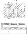
- Fig. 1 is a cross section showing a semiconductor device in accordance with the first example.
- the semiconductor device of Fig. 1 comprises a semiconductor substrate 1, a buried oxide film 2, a semiconductor layer 3, an isolation insulating film 4, a gate insulating film 5, a gate electrode 6, source/drain regions 7, 71, 8, and 81, pocket implantation regions 72 and 82, a sidewall insulating film 9, wires 10 and 110, interlayer insulating films 11 and 111, a p-type impurity region 12, a contact hole 13 and a silicon nitride film 14.
- the semiconductor layer 3 (the first semiconductor region) below the isolation insulating film 4 is particularly represented as 3a.
- Fig. 2 is a plan view showing the semiconductor device in accordance with the first example.
- Fig. 1 is the cross section taken along the section A-A of Fig. 2.
- the interlayer insulating films 11 and 111, the silicon nitride film 14, the wire 10, the sidewall insulating film 9, the source/drain regions 71 and 81 and the pocket implantation regions 72 and 82 are omitted for convenience of illustration.
- a structure in which the semiconductor layer 3 is formed entirely over the semiconductor substrate 1 with the buried oxide film 2 interposed therebetween is termed an SOI substrate, which can be formed by any method of bonding method, the SIMOX method and the like.
- the buried oxide film 2 has a thickness of about 100 to 500 nm
- the semiconductor layer 3 has a thickness of about 30 to 400 nm containing a p-type impurity such as boron of about 1 ⁇ 10 15 to 1 ⁇ 10 18 /cm 3 .
- Active regions in which the transistors are formed are surrounded by a partial isolation region consisting of the p-type impurity region 12 and the isolation insulating film 4 (PTI) which is a silicon oxide film or the like, being isolated from one another.
- a minimum isolation width is about 200 nm.
- the isolation insulating film 4 has a thickness of about half to one third of that of the semiconductor layer 3, and is set so that the thickness of the semiconductor layer 3a therebelow should be about 15 to 200 nm.
- the level of an upper surface of the isolation insulating film 4 should be equal to that of a surface of the semiconductor layer 3, when the semiconductor layer 3 is thin, making the level of the upper surface of the isolation insulating film 4 higher than that of the surface of the semiconductor layer 3 improves isolation performance since it becomes difficult to ensure the thickness sufficient for isolation if sufficient thickness of the semiconductor layer 3a below the isolation insulating film 4 is left.
- a silicon oxide film is used as the isolation insulating film 4 herein, other insulating films, such a silicon nitride film, a silicon oxynitride film, a silicon oxide film containing fluorine and a porous silicon oxide film, may be used.
- a silicon oxide film having a thickness of about 5 to 30 nm as needed (not shown).
- the source/drain regions 7, 8, 71 and 81, the pocket implantation regions 72 and 82 and the p-type impurity region 12 are formed by implanting an impurity into the p-type semiconductor layer 3, and the p-type impurity region 12 contains boron or the like of about 1 ⁇ 10 17 to 1 ⁇ 10 18 /cm 3 . Further, the pocket implantation regions 72 and 82 each contains B, BF 2 or In of about 1 ⁇ 10 17 to 1 ⁇ 10 19 /cm 3 . The pocket implantation regions 72 and 82 serve to suppress a short channel effect and are not needed if the depth of junction of the gate insulating film and the source/drain regions is optimized.
- the source/drain regions 7 and 8 each containing an n-type impurity such as arsenic of about 1 ⁇ 10 19 to 1 ⁇ 10 21 /cm 3 and the source/drain regions 71 and 81 each containing an n-type impurity such as phosphorus of about 1 ⁇ 10 18 to 1 ⁇ 10 20 /cm 3 constitute an LDD (Lightly Doped Drain) structure.
- the LDD structure is formed as needed. Further, though Fig. 1 shows the source/drain regions 7 and 8 reaching the buried oxide film 2, these may not reach the buried oxide film 2.
- SiO 2 , SiON a layered film consisting of SiO 2 , Si 3 N 4 and SiO 2 (ONO), Ta 2 O 5 , Al 2 O 3 , a BST film (Ba x Sr 1-x TiO 3 : Barium Strontium Titanium) or the like may be used.
- the gate electrode 6 contains an n-type impurity such as phosphorus of about 2 to 15 ⁇ 10 20 /cm 3 and is made of polysilicon having a thickness of about 100 to 400nm, it may be made of, instead of polysilicon, a layered structure consisting of a polysilicon containing an impurity and a metal silicide layer such as TiSi 2 , CoSi 2 , NiSi 2 , WSi 2 , TaSi 2 , MoSi 2 , HfSi 2 , Pd 2 Si, PtSi 2 or ZrSi 2 , or a metal such as W, Mo, Cu or Al, and further may be made of a metal such as W, Mo, Cu or Al.
- a metal silicide layer such as TiSi 2 , CoSi 2 , NiSi 2 , WSi 2 , TaSi 2 , MoSi 2 , HfSi 2 , Pd 2 Si, PtSi 2 or ZrSi
- a metal silicide such as TiSi 2 , CoSi 2 , NiSi 2 , WSi 2 , TaSi 2 , MoSi 2 , HfSi 2 , Pd 2 Si, PtSi 2 or ZrSi 2 may be formed (not shown).
- the sidewall insulating film 9 is made of a silicon oxide film, a TEOS film, a Si 3 N 4 film or a layered film consisting of Si 3 N 4 and SiO 2 , and a film containing nitrogen, such as the Si 3 N 4 film or the layered film consisting of Si 3 N 4 and SiO 2 eliminates the possibility of being etched even through a mask displacement in forming the contact hole 13.
- the synergistic effect with the silicon nitride film 14 it is possible to improve the density of micro-defects caused by stress in the semiconductor layer 3 which is to become a channel formation region near the source/drain regions 7 and 71 serving as a source region or the source/drain regions 8 and 81 and carriers (positive hole in an nMOS and electrons in a pMOS) are not easily accumulated near the source region, to further suppress the floating-body effect.
- the interlayer insulating films 11 and 111 are each made of a silicon oxide film formed by the plasma CVD method, the LPCVD (Low Pressure Chemical Vapor Deposition) method, the atmospheric pressure CVD method or the like.
- the interlayer insulating film 11 has a thickness of about 10 to 300 nm and the interlayer insulating film 111 has a thickness of about 100 to 2000 nm.
- the interlayer insulating films 11 and 111 may be made of a TEOS film or a SOG (Spin On Glass) film, and further may be made of a PSG (Phospho Silicate Glass), a BSG (Boro silicate Glass), a BPSG (Boro Phospho Silicate Glass) or a BPTEOS (Boro Phospho TEOS), all of which contain an impurity, instead of the silicon oxide film.
- the silicon nitride film 14 has a thickness of about 50 to 100 nm and is entirely formed except a portion where the contact holes 13 each having a diameter of 0.1 to 0.5 ⁇ m are formed. With the presence of the silicon nitride film 14, micro-defects are formed in the semiconductor layer 3 below the isolation insulating film 4.
- Fig. 3 is a cross section showing the semiconductor device in accordance with the first example and an enlarged view of a portion enclosed by the broken line B in Fig. 1. As shown in Fig. 3, the micro-defect is formed in the semiconductor layer 3a below the isolation insulating film 4.
- the silicon nitride film is made of Si 3 N 4 having a stress of about 1 ⁇ 10 11 dyn/cm 2 , and the film stress can be controlled depending on the ratio of N to Si of Si x N y . Further, since the film stress can be also controlled by adding O to change the composition ratio of O and N, a silicon oxynitride film (SiON) may be formed, instead of the silicon nitride film.
- SiON silicon oxynitride film
- a gate voltage V G is about 1.8 V
- a drain voltage V D is about 1.8 V
- a source voltage V S is about 0 V
- a body voltage (the voltage to be applied to the wire 110) V B is about 0 V.
- a channel is formed in a surface of the semiconductor layer 3 below the gate electrode 6, and one of the source/drain region 7 or 71 and the source/drain region 8 or 81 serves as the source region and the other serves as the drain region, which operates as a circuit.
- the semiconductor layer 3a below the isolation insulating film 4 contains a p-type impurity like the semiconductor layer 3 below the gate electrode 6 and the impurity region 12 and is electrically connected to the semiconductor layer 3 below the gate electrode 6 and provided adjacently to these two, a voltage is applied to the semiconductor layer 3 below the gate electrode 6 from the wire 110 through the impurity region 12.
- Those voltage values are examples, and can vary depending on the thickness of the gate insulating film and the gate length.
- the semiconductor layer 3 contains an n-type impurity such as phosphorus or arsenic
- the source/drain regions 7, 8, 71 and 81 contain a p-type such as boron
- pocket implantation regions 72 and 82 contain an n-type impurity such as arsenic (As), phosphorus (P) or antimony (Sb)
- the gate electrode 6 contains a p-type impurity such as boron.
- an n-type impurity region is formed, instead of the p-type impurity region 12.
- the gate voltage V G is about 0 V
- the drain voltage V D is about 0 V
- the source voltage V S is about 1.8 V
- the body voltage V B is about 1.8 V.
- the number of layers of the interlayer insulating films formed between the wire and the transistor and the arrangement are changed depending on the circuit configuration. Further, though the discussion is made taking an example of the semiconductor device in which one transistor is formed in one active region, the configuration is not limited to this.
- the isolation performance can be improved only if the silicon nitride film 14 is formed in a region in which the PTI is used as device isolation in a semiconductor device in which the PTI and the FTI are used together (not shown).
- Fig. 4 is a cross section showing another semiconductor device in accordance with the first example, showing a silicon nitride film 141.
- the sidewall insulating film 9 is formed of a film containing nitrogen such as the Si 3 N 4 film or the layered film consisting of Si 3 N 4 and the SiO 2 and as shown in Fig. 4, the silicon nitride film 141 is formed on a surface of the gate electrode 6, it is possible to more surely eliminate the possibility of electrical connection between the gate electrode 6 and the wire 10 even if the wire 10 is formed near the gate electrode 6.
- Fig. 5 is a cross section showing still another semiconductor device in accordance with the first example.
- Fig. 6 is a plan view showing this semiconductor device in accordance with the first example.
- the cross section of Fig. 5 is taken along the section C-C of Fig. 6.
- the semiconductor device comprises the wire 10 connected to both the gate electrode 6 and the source/drain region 7, and the diameter of the contact hole in this portion is twice as large as that in other portions.
- This structure of the semiconductor device is generally referred to as a shared contact structure and is used for an SRAM memory in which the gate electrode 6 and the source/drain region 7 always operate at the same potential.
- the semiconductor device of Figs. 5 and 6 has the same structure as that of Fig. 1 except this interconnection structure.
- Fig. 7 is a cross section showing yet another semiconductor device in accordance with the first example, and the semiconductor device of Fig. 7 comprises an interlayer insulating film 113, a contact hole 131 and a wire 210.
- the wire 210 is connected to the gate electrode 6 through the contact hole 131 formed in the interlayer insulating film 113, and a region where the contact hole 131 is formed has the same structure as that in the semiconductor device of Figs. 1 and 2 except that the isolation insulating film 4 is the FTI reaching the buried oxide film 2.
- Fig. 8 is a plan view showing the semiconductor device of Fig. 7, and Fig. 7 is the cross section taken along the section D-D of Fig. 8. Referring to 8, a portion enclosed by the broken line E is the FTI. In Fig. 8, the interlayer insulating film is not shown for simple illustration.
- the semiconductor device in which the element is formed on the main surface of the SOI substrate consisting of the semiconductor substrate 1 the buried oxide film 2 provided entirely over the surface of the semiconductor substrate 1 and the semiconductor layer 3 provided on the surface of the buried oxide film 2 comprises the silicon nitride film 14 formed on a surface of the element with the interlayer insulating film 11 interposed therebetween, micro-defects which develop into lifetime killers are generated in the semiconductor layer 3a below the isolation insulating film 4 by a stress of the silicon nitride film 14 and this shorten the lifetime of carriers (positive hole in an nMOS and electrons in a pMOS).
- the hot carrier tolerance is deteriorated if the hydrogen enters the gate insulating film 5 and the hydrogen termination occurs at the interface of the semiconductor layer 3, the gate insulating film 5 and the buried oxide film 2 when an annealing under a hydrogen atmosphere in the last step is executed, since the silicon nitride film 14 is formed in the semiconductor device of this example, it is possible to prevent entry of hydrogen into the gate insulating film 5 and the buried oxide film 2 and this improves the hot carrier resistance.
- the film stress of the silicon nitride film or the silicon oxynitride film can be increased and the density of micro-defects generated in the semiconductor layer below the isolation insulating film of PTI can be increased, whereby the function of the lifetime killer can be improved.
- Figs. 9 to 13 are cross sections each showing a process step in the method of manufacturing the semiconductor device in accordance with the first example.
- Fig. 9 shows a silicon oxide film 31, a silicon nitride film 32 and a trench 41.
- the silicon oxide film 31 having a thickness of about 5 to 40 nm is formed on the surface of the semiconductor layer 3 in the SOI substrate which comprises the buried oxide film 2 and the semiconductor layer 3 on the surface of the semiconductor substrate 1.
- a thermal oxidation method a method of forming the TEOS oxide film by the CVD and the like may be used.
- the silicon nitride film 32 having a thickness of about 50 to 300 nm is formed on the silicon oxide film 31 by the LPCVD method or the plasma nitride film CVD method, and the silicon nitride film 32 and the silicon oxide film 31 on an isolation region are selectively removed through anisotropic etching by RIE (Reactive Ion Etching) or ECR (Electron Cyclotron Resonance) device with a photoresist mask (not shown).
- RIE Reactive Ion Etching
- ECR Electro Cyclotron Resonance
- the semiconductor layer 3 is anisotropically etched with the silicon nitride film 32 used as a mask by using RIE or the ECR device, to form the trench 41 having a depth of about 20 to 300 nm in the surface of the semiconductor layer 3.
- the trench 41 has a width of about 100 to 500 nm and is formed so that the semiconductor layer 3 of about 10 to 100 nm should be left therebelow.
- Fig. 9 is the cross
- Fig. 10 shows a trench 42 and a photoresist mask 301.
- the photoresist mask 301 having an opening at a portion in which the FTI is to be formed is formed and a bottom surface of the trench 41 is etched therewith, to form the trench 42 reaching the buried oxide film 2.
- the photoresist mask 301 may be formed inside the trench 41 or may be formed on the surface of the silicon nitride film 32.
- a silicon oxide film is entirely formed to have a thickness of about 100 to 500 nm (not shown) by a plasma TEOS or an HDP (High Density Plasma) apparatus, and thermally treated at about 1000° to 1100 °C, to enhance the film quality. Then, the silicon oxide film on the surface of the silicon nitride film 32 is removed by the CMP (Chemical Mechanical Polishing) method with the silicon nitride film 32 used as a stopper, to leave the silicon oxide film only inside an opening constituted of the trench 41, the silicon oxide film 31 and the silicon nitride film 32.
- CMP Chemical Mechanical Polishing
- the silicon oxide film is etched in order to eliminate the level difference between a surface of the silicon oxide film inside the opening and the surface of the semiconductor layer 3, and then the silicon nitride film 32 is removed by wet etching with thermal phosphoric acid and the silicon oxide film 31 is removed, to form the isolation insulating film 4.
- the semiconductor layer 3 below the isolation insulating film 4 corresponds to the semiconductor layer 3a.
- Fig. 11 is the cross section showing the state at the end of this step. Figs. 11 to 13 show only the PTI structure.
- a corner of the silicon formed by the bottom surface and side surface of the trench 41 and a corner of the silicon formed by the side surface of the trench 41 and the surface of the semiconductor layer 3 are rounded, and this relieves the stress in this portion.
- a silicon oxide film is entirely formed by the thermal oxidation (not shown), and then a photoresist mask (not shown) having an opening at a portion in which the wires are to be formed to fix the potential of the channel formation region is formed.
- a p-type impurity such as B, BF 2 or In is ion-implanted to form the p-type impurity region 12 having an impurity concentration of about 1 ⁇ 10 17 to ⁇ 10 18 /cm 3 .
- an n-type impurity such as P, As or Sb is ion-implanted to form an n-type impurity region.
- an impurity such as boron or boron fluoride in the case of nMOS or an impurity such as phosphorus or arsenic in the pMOS, is entirely ion-implanted at an energy of 10 to 20 keV at a dose of about 1 ⁇ 10 12 to 5 ⁇ 10 12 /cm 2 , to introduce the impurity into the channel formation region for controlling the threshold value (not shown).
- the silicon oxide film is formed in order to protect the surface of the semiconductor substrate from a damage in ion-implantation and removed after this ion implantation.
- a silicon oxide film for example, is formed as the gate insulating film 5 entirely over the surface of the semiconductor layer 3 by the thermal oxidation to have a thickness of about 7 to 10 nm, and a polysilicon layer for the gate electrode 6 is deposited entirely by the LPCVD method to have a thickness of about 100 to 400 nm and patterned with a photoresist mask (not shown) by using an anisotropic etching device such as RIE or ECR, to form the gate electrode 6.
- RIE anisotropic etching device
- a silicon oxide film or a layered film consisting of a silicon nitride film and a silicon oxide film is formed on a surface of the polysilicon layer, this film is once patterned with the photoresist mask, and then the polysilicon layer is processed with the patterned film. Further, there may another case where the metal silicide layer such as WSi is deposited on the surface of the polysilicon layer, and then this film is patterned.
- an impurity such as boron or boron fluoride in the case of nMOS or an impurity such as phosphorus or arsenic in the pMOS, is ion-implanted at a dose of about 1 ⁇ 10 12 to 1 X 10 14 /cm 2 , to form the pocket implantation regions 72 and 82.
- an impurity such as phosphorus or arsenic in the case of nMOS or an impurity such as boron or boron fluoride in the pMOS, is ion-implanted at an energy of 20 to 40 keV at a dose of about 10 14 to 10 15 /cm 2 , to form the source/drain regions 71 and 81.
- a silicon oxide film is entirely deposited by the plasma CVD method to have a thickness of about 30 to 100 nm and etched back, to form the sidewall insulating film 9, and after that, an impurity such as arsenic in the case of nMOS or an impurity such as boron or boron fluoride in the pMOS, is ion-implanted at an energy of 10 keV at a dose of about 1 ⁇ 10 14 to 1 ⁇ 10 16 /cm 2 , to form the source/drain regions 7 and 8.
- Fig. 12 is the cross section showing the element of the semiconductor device at the end of this step.
- the TEOS film may be used, or the Si 3 N 4 or the layered film consisting of Si 3 N 4 and SiO 2 may be formed by the LPCVD method or the plasma CVD method.
- the Si 3 N 4 or the layered film consisting of Si 3 N 4 and SiO 2 may be formed by the LPCVD method or the plasma CVD method.
- the layered film a silicon oxide film is formed by RTO (Rapid Thermal Oxidation) and a silicon nitride film is deposited thereon by the CVD method and etched back.
- the source/drain regions may have an LDD structure as needed, in some cases, no source/drain region 7 or 8 is formed.
- the implanted impurity is annealed at about 800° to 1150 °C for about 10 to 30 minutes to be activated.
- metal silicide layer such as CoSi 2 is formed on the surfaces of the gate electrode 6 and the source/drain regions 7 and 8
- cobalt should be entirely deposited and the RTA (Rapid Thermal Anneal) is performed in this stage. This causes the silicon to react on the exposed surfaces of the gate electrode 6 and the source/drain regions 7 and 8, whereby the metal silicide layer is formed in this portion. After that, the unreacted cobalt is removed (not shown).
- metal silicides such as TiSi 2 , Nisi 2 , WSi 2 , TaSi 2 , MoSi 2 , HfSi 2 , PdSi, PtSi 2 and ZrSi 2 may be used.
- Fig. 13 shows a photoresist mask 302.
- a silicon oxide film for the interlayer insulating film 11 is deposited by the plasma CVD method, the LPCVD method, the atmospheric pressure CVD method or the like to have a thickness of about 10 to 300 nm
- the interlayer insulating film 11 may be made of a TEOS film, a SOG film, and further may be made of a PSG, a BSG, a BPSG or a BPTEOS, all of which contain an impurity, instead of the silicon oxide film.
- the above steps of depositing an oxide film can be omitted as needed.
- the silicon nitride film 14 is formed by the LPCVD method (at 600° to 800 the plasma CVD method (at 300° to 500 °C), the atmospheric pressure CVD method (at 300° to 500 °C) or the like to have a thickness of about 50 to 100 nm.
- the silicon nitride film Si 3 N 4 SiO x N y may be used, and the composition of Si and N may be made different from that of Si 3 N 4 .
- a film formed by the LPCVD method has advantages of good uniformity in film thickness and high denseness and chemical stability.
- a film formed by the plasma CVD method or the atmospheric pressure CVD method which can be formed at low temperature, can advantageously suppress the TED (Transient Enhanced Diffusion) of the impurity and therefore improve the current driving capability of a transistor. Further, in the plasma CVD method, it is easy to control the composition ratio of Si and N of the silicon nitride film and therefore it becomes easy to control the stress.
- TED Transient Enhanced Diffusion
- the interlayer insulating film 111 is formed to have a thickness of about 100 to 2000 nm in the same manner as the interlayer insulating film 11 and then planarized by the CMP method. After the planarization, to eliminate the raggedness in the surface through the CMP, a silicon oxide film is deposited again to have a thickness of about 50 to 200 nm in the same manner as the interlayer insulating film 11 is formed (not shown).
- H 2 and CO may be used as an additive gas.
- Fig. 13 is the cross section showing the element of the semiconductor device at the end of this step.
- the remaining silicon nitride film 14 and interlayer insulating film 11 are etched under the condition of lower selection ratio of the silicon nitride film and the silicon oxide film, to dig the trench 13 deeper, whereby the contact hole 13 is formed.
- tungsten (W) is deposited by the blanket CVD method, to fill the inside of the contact hole 13 and etched back for planarization.
- aluminum (Al) is entirely deposited and patterned, to form the wires 10 and 110 made of W and Al, whereby the semiconductor device shown in Fig. 1 is obtained.
- an interlayer insulating film and a wire are further layered in the same process as the interlayer insulating film 111 and the wires 10 and 110 are formed (not shown).
- the method of depositing W for the wires 10 and 110 may be a selective CVD method, or instead of W, Al may be deposited by high-temperature sputtering or reflow sputtering, or TiN or doped polysilicon may be deposited by the LPCVD method. Instead of Al, AlCuSi, Cu or doped polysilicon may be used.
- a barrier metal made of TiN or the like is formed on an inner wall of each contact hole to prevent the metal from diffusing onto the semiconductor layer 3.
- the contact holes and the wires connected to the source/drain regions and the p-type impurity region are formed in the same process step in this example, the contact holes and the wires may be formed in different steps according to a circuit configuration and the order of formation may be changed as needed.
- the metal silicide layer when the metal silicide layer is formed on the surfaces of the source/drain regions 7 and 8 by salicide method, the metal silicide layer serves as an etching stopper in etching the interlayer insulating film 11 and therefore the etching margin increases.
- the semiconductor device in which the element is formed on the main surface of the SOI substrate consisting of the semiconductor substrate 1 the buried oxide film 2 provided entirely over the surface of the semiconductor substrate 1 and the semiconductor layer 3 provided on the surface of the buried oxide film 2 comprises the silicon nitride film 14 formed on a surface of the element with the interlayer insulating film 11 interposed therebetween, micro-defects which develop into lifetime killers are generated in the semiconductor layer 3a below the isolation insulating film 4 by a stress of the silicon nitride film 14 and this shorten the lifetime of carriers (positive hole in an nMOS and electrons in a pMOS).
- the hot carrier resistance is deteriorated if the hydrogen enters the gate insulating film 5 and the hydrogen termination occurs at the interface of the semiconductor layer 3 and the gate insulating film 5, since the silicon nitride film 14 is formed in the semiconductor device of this example, it is possible to prevent entry of hydrogen into the gate insulating film 5 and the buried oxide film 2, whereby the semiconductor device of improved hot carrier resistance can be manufactured.
- the above feature has a high degree of effectiveness on a SOI substrate comprising two oxide films (gate insulating film and buried oxide film) having an effect on device properties as compared to a bulk substrate.
- the thick interlayer insulating film 111 on the silicon nitride film 14 and the thin interlayer insulating film 11 below the silicon nitride film 14 are separately etched with the silicon nitride film 14 to form the contact holes, it is possible to prevent overetching of the semiconductor layer by controlling the etching condition of the interlayer insulating film below the silicon nitride film, whereby the semiconductor device which has no possibility of generating the junction leak current can be obtained.
- Figs. 14 and 15 are cross sections each showing a semiconductor device in accordance with the second example.
- Fig. 14 shows a p well 33, an n well 34, n-type source/drain regions 73, 74, 83 and 84, p-type pocket implantation regions 75 and 85, p-type source/drain regions 76, 77, 86 and 87, n-type pocket implantation regions 78 and a p-type impurity region 121 and an n-type impurity region 122.
- the p well 33 and the n well 34 below the isolation insulating film 4 are particularly represented as 33a and 34a, respectively.
- an nMOS transistor is formed in the p well 33 which is formed by implanting ions into the semiconductor layer and a pMOS transistor is formed in the n well 34, forming a CMOS structure.
- the nMOS transistor and the pMOS transistor are isolated from each other by a PTI and the channel formation regions of the nMOS transistor and the pMOS transistor are connected to the p-type impurity region 121 and the n-type impurity region 122, respectively, through the semiconductor layer below the PTI and the potentials thereof are fixed.
- the p well 33 contains an impurity such as B, BF 2 or In of about 1 ⁇ 10 15 to 1x 10 19 /cm 3
- the n well 34 contains an impurity such as P, AS or Sb of about 1 ⁇ 10 15 to 1 ⁇ 10 19 /cm 3 .
- the polysilicon layer contains an n-type impurity such as phosphorus of about 2 to 15 ⁇ 10 20 /cm 3 , like in the first example, while the impurity contained in the polysilicon of the gate electrode 6 in the pMOS transistor may be a p-type impurity such as boron in some cases (Dual Gate structure) and may be an n-type impurity in other cases (Single Gate structure).
- the film thicknesses and impurity concentrations of constituent elements, other than the above, are the same as those in the semiconductor device of the first example.
- the semiconductor device in which the element is formed on the main surface of the SOI substrate consisting of the semiconductor substrate 1 the buried oxide film 2 provided entirely over the surface of the semiconductor substrate 1 and the semiconductor layer 3 provided on the surface of the buried oxide film 2 comprises the silicon nitride film 14 formed on a surface of the element with the interlayer insulating film 11 interposed therebetween, micro-defects which develop into lifetime killers are generated in the semiconductor layer 3a below the isolation insulating film 4 by a stress of the silicon nitride film 14 and this shorten the lifetime of carriers (positive hole in an nMOS and electrons in a pMOS).
- the thickness of the semiconductor layer 3 (p well region 33 (the first semiconductor region), n well region 34 (the second semiconductor region)) below the isolation insulating film 4 becomes thinner, a potential of the channel formation region below the gate electrode 6 can be stably fixed and a floating-body effect, such as the frequency dependency of delay time, can be suppressed, whereby the reliability of the semiconductor device can be improved.
- the breakdown voltage between the p well 33 and the n well 34 which are adjacent to each other increases due to micro-defects which are generated in the third semiconductor region below the isolation insulating film 4 and develops into a lifetime killer, whereby the reliability of the semiconductor device can be advantageously improved.
- the hot carrier resistance is deteriorated if the hydrogen enters the gate insulating film 5 (the buried oxide film 2) and the hydrogen termination occurs at the interface of the semiconductor layer 3 and the gate insulating film 5, since the silicon nitride film 14 is formed in the semiconductor device of this preferred embodiment, it is possible to prevent entry of hydrogen into the gate insulating film 5 and the buried oxide film 2 and this improves the hot carrier resistance.
- the latch-up resistance can be improved though the manufacturing process becomes complicated.
- Fig. 16 is a cross section showing a process step in a method of manufacturing a semiconductor device in accordance with the second example.
- Fig. 16 shows a photoresist mask 303.
- the isolation insulating film 4 is formed on the surface of the SOI substrate in which the semiconductor layer 3 is provided on the surface of the semiconductor substrate 1 with the buried oxide film 2 interposed therebetween.
- the photoresist mask 303 having an opening for the nMOS region is formed and a p-type impurity such as B, BF 2 or In is ion-implanted, to form the p well 33 having an impurity concentration of about 1 ⁇ 10 15 to 1 ⁇ 10 19 /cm 3 .
- Fig. 16 is the cross section showing the element of the semiconductor device at the end of this step. After that, the photoresist mask 303 is removed.
- a photoresist mask having an opening for the pMOS region is formed and an n-type impurity such as P, As or Sb is entirely ion-implanted, to form the n well 34 having an impurity concentration of about 1 ⁇ 10 15 to 1 ⁇ 10 19 /cm 3 (not shown). After that, the photoresist mask is removed.
- the p-type impurity region 121 and the n-type impurity region 122 are formed.
- the semiconductor device in which the element is formed on the main surface of the SOI substrate consisting of the semiconductor substrate 1 the buried oxide film 2 provided entirely over the surface of the semiconductor substrate 1 and the semiconductor layer 3 provided on the surface of the buried oxide film 2 comprises the silicon nitride film 14 formed on a surface of the element with the interlayer insulating film 11 interposed therebetween, micro-defects which develop into lifetime killers are generated in the semiconductor layer 3a below the isolation insulating film 4 by a stress of the silicon nitride film 14 and this shorten the lifetime of carriers (positive hole in an nMOS and electrons in a pMOS).
- the breakdown voltage between the p well 33 and the n well 34 which are adjacent to each other increases due to micro-defects generated in the semiconductor layer below the isolation insulating film, to increase latch-up resistance, whereby the reliability of the semiconductor device can be advantageously improved.
- the hot carrier resistance is deteriorated if the hydrogen enters the gate insulating film 5 and the hydrogen termination occurs at the interface of the semiconductor layer 3 and the gate insulating film 5, since the silicon nitride film 14 is formed in the semiconductor device of this preferred embodiment, it is possible to prevent entry of hydrogen into the gate insulating film 5 and the buried oxide film 2, whereby the method of manufacturing the semiconductor device of increased hot carrier resistance can be obtained.
- the thick interlayer insulating film 111 on the silicon nitride film 14 and the thin interlayer insulating film 11 below the silicon nitride film 14 are separately etched with the silicon nitride film 14 to form the contact holes, it is possible to prevent overetching of the semiconductor layer by controlling the etching condition of the interlayer insulating film 1I below the silicon nitride film 14, whereby the semiconductor device which has no possibility of generating the junction leak current can be obtained.
- Fig. 17 is a cross section showing a semiconductor device in accordance with the preferred embodiment of the present invention.
- Fig. 17 shows contact holes 132 and wires 310.
- the interlayer insulating films 11 and 111 and the contact holes 132 formed in the silicon nitride film 14 are formed across the surfaces of the source/drain regions 7 and 8 and the isolation insulating film 4, and the wires 310 connected to the source/drain regions 7 and 8 through the contact holes 132 are also formed on th surface of the isolation insulating film 4.
- the present structure of the preferred embodiment is the same as that of the first example.
- Fig. 18 is a plan view showing the semiconductor device in accordance with the preferred embodiment of the present invention, and Fig. 17 is the cross section taken along the section F-F of Fig. 18.
- the interlayer insulating films 11 and 111, the silicon nitride film 14, the wires 110 and 310, the sidewall insulating film 9, the source/drain regions 71 and 81 and the pocket implantation regions 72 and 82 are omitted, for convenience of illustration.
- the semiconductor device of the preferred embodiment which has a borderless contact structure in which the wires 310 connected to the source/drain regions 7 and 8 are formed across the adjacent isolation insulating films 4, comprises the silicon nitride film 14, the isolation insulating film 4 is prevented from being etched when the contact holes 132 reaching the source/drain regions 7 and 8 are formed and sufficient distances from the pn junctions between the semiconductor layer 3a and the source/drain regions 7 and 8 to the wires 310 can be ensured, whereby the semiconductor device of higher element density and higher reliability can be obtained.
- the semiconductor device in which the element is formed on the main surface of the SOI substrate consisting of the semiconductor substrate 1 the buried oxide film 2 provided entirely over the surface of the semiconductor substrate 1 and the semiconductor layer 3 provided on the surface of the buried oxide film 2 comprises the silicon nitride film 14 formed on a surface of the element with the interlayer insulating film 11 interposed therebetween, micro-defects which develop into lifetime killers are generated in the semiconductor layer 3a below the isolation insulating film 4 by a stress of the silicon nitride film 14 and this shorten the lifetime of carriers (positive hole in an nMOS and electrons in a pMOS).
- the thickness of the semiconductor layer 3a below the isolation insulating film 4 becomes thinner, a potential of the channel formation region below the gate electrode 6 can be stably fixed and a floating-body effect, such as the frequency dependency of delay time, can be suppressed, whereby the reliability of the semiconductor device can be improved.
- the hot carrier resistance is deteriorated if the hydrogen enters the gate insulating film 5 and the hydrogen termination occurs at the interface of the semiconductor layer 3 and the gate insulating film 5, since the silicon nitride film 14 is formed in the semiconductor device of this preferred embodiment, it is possible to prevent entry of hydrogen into the gate insulating film 5 and the buried oxide film 2 and this improves the hot carrier resistance.
- Fig. 19 is a cross section showing another semiconductor device in accordance with the preferred embodiment of the present invention, showing an n-type partial impurity region 123.
- the n-type impurity region 123 contains an impurity such as P, As or Sb of about 1 ⁇ 10 15 to 1 ⁇ 10 19 /cm 3 , and is connected to the source/drain region 7 and extends towards the central portion of the isolation insulating film 4 relative to a region where the contact hole 132 is formed on the isolation insulating film 4.
- the n-type impurity region 123 can be formed by diagonally implanting ions after forming the contact hole 132.
- the present structure of the preferred embodiment is the same as that of the semiconductor device of Fig. 17.
- the exposed isolation insulating film 4 is likely to be etched in forming the contact hole 132.
- the n-type impurity region 123 it is possible to ensure sufficient distance between the wire 310 and the p-type semiconductor layer 3 and eliminate the possibility of generating the leak current at a junction between the semiconductor layer 3a and the n-type impurity region 123.
- Fig. 20 is a plan view showing still another semiconductor device in accordance with the preferred embodiment of the present invention.
- the structure of this semiconductor device is the same as that of the semiconductor device shown in Fig. 17, except that the isolation insulating film 4 is an FTI reaching the buried oxide film 2 in a portion enclosed by the broken line G.
- the isolation insulating film 4 is an FTI reaching the buried oxide film 2 in a portion enclosed by the broken line G.
- the isolation insulating film 4 is an FTI reaching the buried oxide film 2 in a portion enclosed by the broken line G.
- the isolation performance can be improved only if the silicon nitride film 14 is formed in a region in which the PTI is used as device isolation in a semiconductor device in which the PTI and the FTI are used together.
- the shape of the isolation insulating film 4 can be kept only if the silicon nitride film 14 is formed on a surface of a portion where the wire 310 is formed across the surfaces of the source/drain regions 7 and 8 and the isolation insulating film 4.
- borderless contact structure can be applied to the semiconductor devices in the first and second examples and produce the same effect.
- Fig. 21 is a cross section showing a process step in a method of manufacturing a semiconductor device in accordance with the preferred embodiment of the present invention.
- Fig. 21 shows a photoresist mask 304.
- the isolation insulating film 4, the p-type impurity region (n-type impurity region in the case of pMOS), the gate insulating film 5, the gate electrode 6, the pocket implantation regions 72 and 82, the source/drain regions 71 and 81, the sidewall insulating film 9 and the source/drain regions 7 and 8 are formed on the surface of the SOI substrate in which the semiconductor layer 3 is formed on the surface of the semiconductor substrate 1 with the buried oxide film 2 interposed therebetween.
- the interlayer insulating film 11, the silicon nitride film 14 and the interlayer insulating film 111 are formed in the same manner as in the first example, and these are planarized by the CMP method.
- a silicon oxide film is deposited again to have a thickness of about 50 to 200 nm in the same manner as the interlayer insulating film 1I is formed (not shown).
- the interlayer insulating film 111 is etched in the same manner as in the first example.
- the photoresist mask 304 is patterned so that the contact hole 132 can be formed not only on the surface of the source/drain regions 7 and 8 but also on the surface of the isolation insulating film 4.
- Fig. 21 is the cross section showing the element of the semiconductor device at the end of this step.
- the remaining silicon nitride film 14 and interlayer insulating film 11 are etched under the condition of lower selection ratio of the silicon nitride film and the silicon oxide film, to form the contact holes 132 and 13.
- the wires 110 and 310 are formed in the same manner as in the first preferred embodiment, to form the semiconductor device shown in Fig. 17.
- the thick interlayer insulating film 111 on the silicon nitride film 14 and the thin interlayer insulating film 11 below the silicon nitride film 14 are separately etched with the silicon nitride film 14 to form the contact holes in the semiconductor device having a borderless contact structure in which the wires connected to the source/drain regions are formed across the adjacent isolation insulating films, the overetching of the semiconductor layer can be prevented by controlling the etching condition of the interlayer insulating film below the silicon nitride film 14 and therefore a semiconductor device which has no possibility of generating a junction leak current can be obtained.
- the isolation insulating film 4 is prevented from being etched when the contact holes 132 reaching the source/drain regions 7 and 8 are formed and sufficient distances from the pn junctions between the semiconductor layer 3a and the source/drain regions 7 and 8 to the wires can be ensured, whereby the semiconductor device of higher element density and higher reliability can be obtained.
- the semiconductor device in which the element is formed on the main surface of the SOI substrate consisting of the semiconductor substrate 1 the buried oxide film 2 provided entirely over the surface of the semiconductor substrate 1 and the semiconductor layer 3 provided on the surface of the buried oxide film 2 comprises the silicon nitride film 14 formed on a surface of the element with the interlayer insulating film interposed therebetween, micro-defects which develop into lifetime killers are generated in the semiconductor layer 3 a below the isolation insulating film 4 by a stress of the silicon nitride film 14 and this shorten the lifetime of carriers (positive hole in an nMOS and electrons in a pMOS).
- the hot carrier resistance is deteriorated if the hydrogen enters the gate insulating film 5 and the hydrogen termination occurs at the interface of the semiconductor layer 3 and the gate insulating film 5, since the silicon nitride film 14 is formed in the semiconductor device of this preferred embodiment, it is possible to prevent entry of hydrogen into the gate insulating film 5 and the buried oxide film 2, whereby the method of manufacturing the semiconductor device of improved hot carrier resistance can be obtained.
Landscapes
- Engineering & Computer Science (AREA)
- Physics & Mathematics (AREA)
- Condensed Matter Physics & Semiconductors (AREA)
- General Physics & Mathematics (AREA)
- Manufacturing & Machinery (AREA)
- Computer Hardware Design (AREA)
- Microelectronics & Electronic Packaging (AREA)
- Power Engineering (AREA)
- Thin Film Transistor (AREA)
- Element Separation (AREA)
- Internal Circuitry In Semiconductor Integrated Circuit Devices (AREA)
- Metal-Oxide And Bipolar Metal-Oxide Semiconductor Integrated Circuits (AREA)
Applications Claiming Priority (2)
| Application Number | Priority Date | Filing Date | Title |
|---|---|---|---|
| JP2000171818 | 2000-06-08 | ||
| JP2000171818A JP4776755B2 (ja) | 2000-06-08 | 2000-06-08 | 半導体装置およびその製造方法 |
Publications (2)
| Publication Number | Publication Date |
|---|---|
| EP1168430A1 EP1168430A1 (en) | 2002-01-02 |
| EP1168430B1 true EP1168430B1 (en) | 2005-05-04 |
Family
ID=18674322
Family Applications (1)
| Application Number | Title | Priority Date | Filing Date |
|---|---|---|---|
| EP00128270A Expired - Lifetime EP1168430B1 (en) | 2000-06-08 | 2000-12-22 | Semiconductor device and method of manufacturing the same |
Country Status (7)
| Country | Link |
|---|---|
| US (3) | US6933565B2 (zh) |
| EP (1) | EP1168430B1 (zh) |
| JP (1) | JP4776755B2 (zh) |
| KR (1) | KR100385666B1 (zh) |
| CN (2) | CN1252830C (zh) |
| DE (1) | DE60019913T2 (zh) |
| TW (1) | TW510055B (zh) |
Families Citing this family (39)
| Publication number | Priority date | Publication date | Assignee | Title |
|---|---|---|---|---|
| JP3575408B2 (ja) | 2000-08-15 | 2004-10-13 | セイコーエプソン株式会社 | トレンチ素子分離領域を有する半導体装置の製造方法 |
| US6787422B2 (en) * | 2001-01-08 | 2004-09-07 | Chartered Semiconductor Manufacturing Ltd. | Method of body contact for SOI mosfet |
| JP2003045874A (ja) * | 2001-07-27 | 2003-02-14 | Semiconductor Energy Lab Co Ltd | 金属配線およびその作製方法、並びに金属配線基板およびその作製方法 |
| US7022561B2 (en) * | 2002-12-02 | 2006-04-04 | Taiwan Semiconductor Manufacturing Company, Ltd. | CMOS device |
| JP2004260073A (ja) * | 2003-02-27 | 2004-09-16 | Seiko Epson Corp | 半導体装置およびその製造方法 |
| JP2004281631A (ja) * | 2003-03-14 | 2004-10-07 | Renesas Technology Corp | 半導体装置の設計方法 |
| JP2004348044A (ja) * | 2003-05-26 | 2004-12-09 | Seiko Epson Corp | 表示装置、表示方法及び表示装置の製造方法 |
| US6905941B2 (en) * | 2003-06-02 | 2005-06-14 | International Business Machines Corporation | Structure and method to fabricate ultra-thin Si channel devices |
| TWI244729B (en) * | 2003-08-28 | 2005-12-01 | Renesas Tech Corp | Semiconductor memory device and method of manufacturing the same |
| US7135373B2 (en) * | 2003-09-23 | 2006-11-14 | Texas Instruments Incorporated | Reduction of channel hot carrier effects in transistor devices |
| JP4610982B2 (ja) * | 2003-11-11 | 2011-01-12 | シャープ株式会社 | 半導体装置の製造方法 |
| JP2005183686A (ja) | 2003-12-19 | 2005-07-07 | Renesas Technology Corp | 半導体装置およびその製造方法 |
| JP4065855B2 (ja) * | 2004-01-21 | 2008-03-26 | 株式会社日立製作所 | 生体および化学試料検査装置 |
| US7442598B2 (en) * | 2005-06-09 | 2008-10-28 | Freescale Semiconductor, Inc. | Method of forming an interlayer dielectric |
| US7651935B2 (en) * | 2005-09-27 | 2010-01-26 | Freescale Semiconductor, Inc. | Process of forming an electronic device including active regions and gate electrodes of different compositions overlying the active regions |
| US7504289B2 (en) * | 2005-10-26 | 2009-03-17 | Freescale Semiconductor, Inc. | Process for forming an electronic device including transistor structures with sidewall spacers |
| US7420202B2 (en) * | 2005-11-08 | 2008-09-02 | Freescale Semiconductor, Inc. | Electronic device including a transistor structure having an active region adjacent to a stressor layer and a process for forming the electronic device |
| US7884030B1 (en) | 2006-04-21 | 2011-02-08 | Advanced Micro Devices, Inc. and Spansion LLC | Gap-filling with uniform properties |
| US20080054361A1 (en) * | 2006-08-30 | 2008-03-06 | Infineon Technologies Ag | Method and apparatus for reducing flicker noise in a semiconductor device |
| DE102006040762B4 (de) * | 2006-08-31 | 2009-05-07 | Advanced Micro Devices, Inc., Sunnyvale | N-Kanalfeldeffekttransistor mit einer Kontaktätzstoppschicht in Verbindung mit einer Zwischenschichtdielektrikumsteilschicht mit der gleichen Art an innerer Verspannung |
| US8569858B2 (en) * | 2006-12-20 | 2013-10-29 | Freescale Semiconductor, Inc. | Semiconductor device including an active region and two layers having different stress characteristics |
| US7843011B2 (en) * | 2007-01-31 | 2010-11-30 | Freescale Semiconductor, Inc. | Electronic device including insulating layers having different strains |
| JP5117740B2 (ja) * | 2007-03-01 | 2013-01-16 | ルネサスエレクトロニクス株式会社 | 半導体装置の製造方法 |
| DE102007057682A1 (de) * | 2007-11-30 | 2009-06-04 | Advanced Micro Devices, Inc., Sunnyvale | Hybridkontaktstruktur mit Kontakt mit kleinem Aspektverhältnis in einem Halbleiterbauelement |
| US7932152B2 (en) * | 2008-02-05 | 2011-04-26 | Chartered Semiconductor Manufacturing, Ltd. | Method of forming a gate stack structure |
| US7668010B2 (en) * | 2008-02-27 | 2010-02-23 | Macronix International Co., Ltd. | Flash memory having insulating liners between source/drain lines and channels |
| JP5465907B2 (ja) * | 2009-03-27 | 2014-04-09 | ラピスセミコンダクタ株式会社 | 半導体装置 |
| US8680617B2 (en) * | 2009-10-06 | 2014-03-25 | International Business Machines Corporation | Split level shallow trench isolation for area efficient body contacts in SOI MOSFETS |
| CN102110644A (zh) * | 2009-12-23 | 2011-06-29 | 中芯国际集成电路制造(上海)有限公司 | Pmos器件自对准硅化物阻挡膜制程方法 |
| KR101734936B1 (ko) * | 2010-08-27 | 2017-05-15 | 삼성전자주식회사 | 소자분리 막 아래에 저 저항 영역을 갖는 반도체 소자 |
| US8652929B2 (en) * | 2011-12-23 | 2014-02-18 | Peking University | CMOS device for reducing charge sharing effect and fabrication method thereof |
| US9525057B2 (en) | 2012-05-15 | 2016-12-20 | Mitsubishi Electric Corporation | Semiconductor device |
| EP2743965B1 (en) * | 2012-12-13 | 2015-07-08 | Imec | Method for manufacturing semiconductor devices |
| US9472507B2 (en) | 2013-06-17 | 2016-10-18 | Samsung Display Co., Ltd. | Array substrate and organic light-emitting display including the same |
| KR20160034492A (ko) * | 2014-09-19 | 2016-03-30 | 삼성전자주식회사 | 반도체 소자의 패턴 형성 방법 및 이를 이용하여 형성된 반도체 소자 |
| FR3048126B1 (fr) * | 2016-02-18 | 2018-03-09 | Commissariat A L'energie Atomique Et Aux Energies Alternatives | Structure du type photodiode, composant et procede de fabrication d'une structure |
| US10707330B2 (en) * | 2018-02-15 | 2020-07-07 | Globalfoundries Inc. | Semiconductor device with interconnect to source/drain |
| CN109545802B (zh) * | 2018-12-14 | 2021-01-12 | 上海微阱电子科技有限公司 | 一种绝缘体上半导体器件结构和形成方法 |
| US11164740B2 (en) * | 2019-10-09 | 2021-11-02 | Newport Fab, Llc | Semiconductor structure having porous semiconductor layer for RF devices |
Family Cites Families (31)
| Publication number | Priority date | Publication date | Assignee | Title |
|---|---|---|---|---|
| JPS56150853A (en) | 1980-04-25 | 1981-11-21 | Hitachi Ltd | Manufacture of semiconductor device |
| JPS5856450A (ja) | 1981-09-30 | 1983-04-04 | Nec Corp | 相補型mos半導体装置 |
| JPS58124243A (ja) | 1982-01-21 | 1983-07-23 | Toshiba Corp | 半導体装置の製造方法 |
| JP3061907B2 (ja) | 1991-10-01 | 2000-07-10 | 日本電気株式会社 | 半導体装置及びその製造方法 |
| JPH0621373A (ja) | 1992-07-03 | 1994-01-28 | Nec Corp | 半導体装置の製造方法 |
| JPH06347830A (ja) * | 1993-06-07 | 1994-12-22 | Canon Inc | 光透過型半導体装置及びその製造方法 |
| JPH06244180A (ja) | 1993-02-19 | 1994-09-02 | Matsushita Electric Ind Co Ltd | 半導体装置およびその製造方法 |
| JPH0997833A (ja) * | 1995-07-22 | 1997-04-08 | Ricoh Co Ltd | 半導体装置とその製造方法 |
| US5899712A (en) | 1995-08-21 | 1999-05-04 | Hyundai Electronics Industries Co., Ltd. | Method for fabricating silicon-on-insulator device |
| JPH0969610A (ja) | 1995-08-31 | 1997-03-11 | Hitachi Ltd | 集積半導体装置およびその製造方法 |
| US6127261A (en) | 1995-11-16 | 2000-10-03 | Advanced Micro Devices, Inc. | Method of fabricating an integrated circuit including a tri-layer pre-metal interlayer dielectric compatible with advanced CMOS technologies |
| JPH09172072A (ja) * | 1995-12-18 | 1997-06-30 | Nec Corp | 半導体装置及びその製造方法 |
| US5767549A (en) | 1996-07-03 | 1998-06-16 | International Business Machines Corporation | SOI CMOS structure |
| JPH1032266A (ja) | 1996-07-17 | 1998-02-03 | Sony Corp | 半導体装置の製造方法 |
| JP3445495B2 (ja) * | 1997-07-23 | 2003-09-08 | 株式会社東芝 | 半導体装置 |
| JPH1154758A (ja) * | 1997-08-01 | 1999-02-26 | Hitachi Ltd | 半導体集積回路装置およびその製造方法 |
| US6080655A (en) * | 1997-08-21 | 2000-06-27 | Micron Technology, Inc. | Method for fabricating conductive components in microelectronic devices and substrate structures thereof |
| JPH1187723A (ja) | 1997-09-10 | 1999-03-30 | Hitachi Ltd | 半導体集積回路装置の製造方法 |
| JPH11109406A (ja) * | 1997-09-30 | 1999-04-23 | Sanyo Electric Co Ltd | 表示装置とその製造方法 |
| JP4810712B2 (ja) * | 1997-11-05 | 2011-11-09 | ソニー株式会社 | 不揮発性半導体記憶装置及びその読み出し方法 |
| KR100562539B1 (ko) * | 1997-12-19 | 2006-03-22 | 어드밴스드 마이크로 디바이시즈, 인코포레이티드 | 벌크 씨모스 구조와 양립 가능한 에스오아이 구조 |
| US6153043A (en) * | 1998-02-06 | 2000-11-28 | International Business Machines Corporation | Elimination of photo-induced electrochemical dissolution in chemical mechanical polishing |
| JP3382844B2 (ja) * | 1998-04-07 | 2003-03-04 | 日本電気株式会社 | 半導体装置の製造方法 |
| US6025259A (en) * | 1998-07-02 | 2000-02-15 | Advanced Micro Devices, Inc. | Dual damascene process using high selectivity boundary layers |
| JP2000133811A (ja) * | 1998-10-28 | 2000-05-12 | Sony Corp | 薄膜トランジスタの製造方法 |
| JP3506025B2 (ja) * | 1998-11-30 | 2004-03-15 | セイコーエプソン株式会社 | 半導体記憶装置及びその製造方法 |
| TW424314B (en) * | 1999-07-09 | 2001-03-01 | Taiwan Semiconductor Mfg | Interconnection lines for improving thermal conductivity in integrated circuits and method for fabricating the same |
| US6083822A (en) * | 1999-08-12 | 2000-07-04 | Industrial Technology Research Institute | Fabrication process for copper structures |
| US6127228A (en) * | 1999-11-06 | 2000-10-03 | United Silicon Incorporated | Method of forming buried bit line |
| US6372569B1 (en) * | 2000-01-18 | 2002-04-16 | Chartered Semiconductor Manufacturing Ltd. | Selective formation of hydrogen rich PECVD silicon nitride for improved NMOS transistor performance |
| US6362508B1 (en) * | 2000-04-03 | 2002-03-26 | Tower Semiconductor Ltd. | Triple layer pre-metal dielectric structure for CMOS memory devices |
-
2000
- 2000-06-08 JP JP2000171818A patent/JP4776755B2/ja not_active Expired - Fee Related
- 2000-12-06 US US09/729,816 patent/US6933565B2/en not_active Expired - Fee Related
- 2000-12-22 DE DE60019913T patent/DE60019913T2/de not_active Expired - Lifetime
- 2000-12-22 EP EP00128270A patent/EP1168430B1/en not_active Expired - Lifetime
-
2001
- 2001-02-07 TW TW090102669A patent/TW510055B/zh not_active IP Right Cessation
- 2001-02-12 KR KR10-2001-0006688A patent/KR100385666B1/ko not_active IP Right Cessation
- 2001-02-13 CN CNB011034599A patent/CN1252830C/zh not_active Expired - Fee Related
- 2001-02-13 CN CNA2006100095736A patent/CN1832178A/zh active Pending
-
2005
- 2005-06-21 US US11/156,554 patent/US7393731B2/en not_active Expired - Fee Related
-
2008
- 2008-06-02 US US12/131,826 patent/US7838349B2/en not_active Expired - Fee Related
Also Published As
| Publication number | Publication date |
|---|---|
| US6933565B2 (en) | 2005-08-23 |
| US20010050397A1 (en) | 2001-12-13 |
| DE60019913T2 (de) | 2005-09-29 |
| CN1832178A (zh) | 2006-09-13 |
| EP1168430A1 (en) | 2002-01-02 |
| US20080274596A1 (en) | 2008-11-06 |
| KR100385666B1 (ko) | 2003-05-27 |
| US7393731B2 (en) | 2008-07-01 |
| DE60019913D1 (de) | 2005-06-09 |
| CN1252830C (zh) | 2006-04-19 |
| TW510055B (en) | 2002-11-11 |
| JP4776755B2 (ja) | 2011-09-21 |
| KR20010111449A (ko) | 2001-12-19 |
| US7838349B2 (en) | 2010-11-23 |
| CN1329367A (zh) | 2002-01-02 |
| JP2001352042A (ja) | 2001-12-21 |
| US20050253219A1 (en) | 2005-11-17 |
Similar Documents
| Publication | Publication Date | Title |
|---|---|---|
| EP1168430B1 (en) | Semiconductor device and method of manufacturing the same | |
| US6251763B1 (en) | Semiconductor device and method for manufacturing same | |
| US5950090A (en) | Method for fabricating a metal-oxide semiconductor transistor | |
| US6335249B1 (en) | Salicide field effect transistors with improved borderless contact structures and a method of fabrication | |
| US6737308B2 (en) | Semiconductor device having LDD-type source/drain regions and fabrication method thereof | |
| US6624496B2 (en) | Method of forming T-shaped isolation layer, method of forming elevated salicide source/drain region using the same, and semiconductor device having T-shaped isolation layer | |
| KR100296004B1 (ko) | 반도체장치및그제조방법 | |
| US6214656B1 (en) | Partial silicide gate in sac (self-aligned contact) process | |
| US6815300B2 (en) | Method for manufacturing semiconductor device having increased effective channel length | |
| JP2000040797A (ja) | 半導体素子を有する半導体構造体とその形成方法 | |
| US6323103B1 (en) | Method for fabricating transistors | |
| JP3530026B2 (ja) | 半導体装置及びその製造方法 | |
| US6184114B1 (en) | MOS transistor formation | |
| US5753548A (en) | Method for preventing fluorine outgassing-induced interlevel dielectric delamination on P-channel FETS | |
| US6639282B2 (en) | Semiconductor device on silicon-on-insulator and method for manufacturing the semiconductor device | |
| US6699746B2 (en) | Method for manufacturing semiconductor device | |
| US6534393B1 (en) | Method for fabricating local metal interconnections with low contact resistance and gate electrodes with improved electrical conductivity | |
| US5707896A (en) | Method for preventing delamination of interlevel dielectric layer over FET P+ doped polysilicon gate electrodes on semiconductor integrated circuits | |
| US6211021B1 (en) | Method for forming a borderless contact | |
| US7119017B2 (en) | Method for improving interlevel dielectric gap filling over semiconductor structures having high aspect ratios | |
| KR100983514B1 (ko) | 반도체소자 제조 방법 | |
| US6511890B2 (en) | Method of fabricating a semiconductor device | |
| JP2006202860A (ja) | 半導体装置及びその製造方法 | |
| JPH09321287A (ja) | 半導体装置の製造方法 |
Legal Events
| Date | Code | Title | Description |
|---|---|---|---|
| PUAI | Public reference made under article 153(3) epc to a published international application that has entered the european phase |
Free format text: ORIGINAL CODE: 0009012 |
|
| 17P | Request for examination filed |
Effective date: 20010831 |
|
| AK | Designated contracting states |
Kind code of ref document: A1 Designated state(s): DE FR GB Kind code of ref document: A1 Designated state(s): AT BE CH CY DE DK ES FI FR GB GR IE IT LI LU MC NL PT SE TR |
|
| AX | Request for extension of the european patent |
Free format text: AL;LT;LV;MK;RO;SI |
|
| AKX | Designation fees paid |
Free format text: DE FR GB |
|
| GRAP | Despatch of communication of intention to grant a patent |
Free format text: ORIGINAL CODE: EPIDOSNIGR1 |
|
| GRAS | Grant fee paid |
Free format text: ORIGINAL CODE: EPIDOSNIGR3 |
|
| GRAA | (expected) grant |
Free format text: ORIGINAL CODE: 0009210 |
|
| AK | Designated contracting states |
Kind code of ref document: B1 Designated state(s): DE FR GB |
|
| REG | Reference to a national code |
Ref country code: GB Ref legal event code: FG4D |
|
| REG | Reference to a national code |
Ref country code: IE Ref legal event code: FG4D |
|
| REF | Corresponds to: |
Ref document number: 60019913 Country of ref document: DE Date of ref document: 20050609 Kind code of ref document: P |
|
| PG25 | Lapsed in a contracting state [announced via postgrant information from national office to epo] |
Ref country code: GB Free format text: LAPSE BECAUSE OF NON-PAYMENT OF DUE FEES Effective date: 20051222 |
|
| PLBE | No opposition filed within time limit |
Free format text: ORIGINAL CODE: 0009261 |
|
| STAA | Information on the status of an ep patent application or granted ep patent |
Free format text: STATUS: NO OPPOSITION FILED WITHIN TIME LIMIT |
|
| ET | Fr: translation filed | ||
| 26N | No opposition filed |
Effective date: 20060207 |
|
| GBPC | Gb: european patent ceased through non-payment of renewal fee |
Effective date: 20051222 |
|
| REG | Reference to a national code |
Ref country code: FR Ref legal event code: TP |
|
| REG | Reference to a national code |
Ref country code: DE Ref legal event code: R082 Ref document number: 60019913 Country of ref document: DE Representative=s name: PRUEFER & PARTNER GBR, DE |
|
| REG | Reference to a national code |
Ref country code: DE Ref legal event code: R082 Ref document number: 60019913 Country of ref document: DE Representative=s name: PRUEFER & PARTNER GBR, DE Effective date: 20140915 Ref country code: DE Ref legal event code: R081 Ref document number: 60019913 Country of ref document: DE Owner name: RENESAS ELECTRONICS CORPORATION, KAWASAKI-SHI, JP Free format text: FORMER OWNER: MITSUBISHI DENKI K.K., TOKYO, JP Effective date: 20140915 Ref country code: DE Ref legal event code: R082 Ref document number: 60019913 Country of ref document: DE Representative=s name: PRUEFER & PARTNER MBB PATENTANWAELTE RECHTSANW, DE Effective date: 20140915 |
|
| REG | Reference to a national code |
Ref country code: FR Ref legal event code: PLFP Year of fee payment: 16 |
|
| PGFP | Annual fee paid to national office [announced via postgrant information from national office to epo] |
Ref country code: DE Payment date: 20151215 Year of fee payment: 16 |
|
| PGFP | Annual fee paid to national office [announced via postgrant information from national office to epo] |
Ref country code: FR Payment date: 20151110 Year of fee payment: 16 |
|
| REG | Reference to a national code |
Ref country code: FR Ref legal event code: TP Owner name: RENESAS ELECTRONICS CORPORATION, JP Effective date: 20160217 Ref country code: FR Ref legal event code: CA Effective date: 20160217 |
|
| REG | Reference to a national code |
Ref country code: DE Ref legal event code: R119 Ref document number: 60019913 Country of ref document: DE |
|
| REG | Reference to a national code |
Ref country code: FR Ref legal event code: ST Effective date: 20170831 |
|
| PG25 | Lapsed in a contracting state [announced via postgrant information from national office to epo] |
Ref country code: FR Free format text: LAPSE BECAUSE OF NON-PAYMENT OF DUE FEES Effective date: 20170102 |
|
| PG25 | Lapsed in a contracting state [announced via postgrant information from national office to epo] |
Ref country code: DE Free format text: LAPSE BECAUSE OF NON-PAYMENT OF DUE FEES Effective date: 20170701 |