KR102181010B1 - Apparatus and methods for micro-transfer printing - Google Patents
Apparatus and methods for micro-transfer printing Download PDFInfo
- Publication number
- KR102181010B1 KR102181010B1 KR1020207006010A KR20207006010A KR102181010B1 KR 102181010 B1 KR102181010 B1 KR 102181010B1 KR 1020207006010 A KR1020207006010 A KR 1020207006010A KR 20207006010 A KR20207006010 A KR 20207006010A KR 102181010 B1 KR102181010 B1 KR 102181010B1
- Authority
- KR
- South Korea
- Prior art keywords
- delete delete
- semiconductor device
- certain embodiments
- substrate
- transfer device
- Prior art date
- Legal status (The legal status is an assumption and is not a legal conclusion. Google has not performed a legal analysis and makes no representation as to the accuracy of the status listed.)
- Active
Links
Images


Classifications
-
- B—PERFORMING OPERATIONS; TRANSPORTING
- B41—PRINTING; LINING MACHINES; TYPEWRITERS; STAMPS
- B41F—PRINTING MACHINES OR PRESSES
- B41F16/00—Transfer printing apparatus
-
- H—ELECTRICITY
- H01—ELECTRIC ELEMENTS
- H01L—SEMICONDUCTOR DEVICES NOT COVERED BY CLASS H10
- H01L21/00—Processes or apparatus adapted for the manufacture or treatment of semiconductor or solid state devices or of parts thereof
- H01L21/02—Manufacture or treatment of semiconductor devices or of parts thereof
- H01L21/04—Manufacture or treatment of semiconductor devices or of parts thereof the devices having potential barriers, e.g. a PN junction, depletion layer or carrier concentration layer
- H01L21/50—Assembly of semiconductor devices using processes or apparatus not provided for in a single one of the groups H01L21/18 - H01L21/326 or H10D48/04 - H10D48/07 e.g. sealing of a cap to a base of a container
- H01L21/52—Mounting semiconductor bodies in containers
-
- B—PERFORMING OPERATIONS; TRANSPORTING
- B25—HAND TOOLS; PORTABLE POWER-DRIVEN TOOLS; MANIPULATORS
- B25J—MANIPULATORS; CHAMBERS PROVIDED WITH MANIPULATION DEVICES
- B25J15/00—Gripping heads and other end effectors
-
- B—PERFORMING OPERATIONS; TRANSPORTING
- B41—PRINTING; LINING MACHINES; TYPEWRITERS; STAMPS
- B41F—PRINTING MACHINES OR PRESSES
- B41F16/00—Transfer printing apparatus
- B41F16/0006—Transfer printing apparatus for printing from an inked or preprinted foil or band
- B41F16/004—Presses of the reciprocating type
- B41F16/0046—Presses of the reciprocating type with means for applying print under heat and pressure, e.g. using heat activable adhesive
-
- B—PERFORMING OPERATIONS; TRANSPORTING
- B41—PRINTING; LINING MACHINES; TYPEWRITERS; STAMPS
- B41F—PRINTING MACHINES OR PRESSES
- B41F16/00—Transfer printing apparatus
- B41F16/0006—Transfer printing apparatus for printing from an inked or preprinted foil or band
- B41F16/006—Arrangements for moving, supporting or positioning the printing foil or band
-
- B—PERFORMING OPERATIONS; TRANSPORTING
- B41—PRINTING; LINING MACHINES; TYPEWRITERS; STAMPS
- B41F—PRINTING MACHINES OR PRESSES
- B41F16/00—Transfer printing apparatus
- B41F16/0006—Transfer printing apparatus for printing from an inked or preprinted foil or band
- B41F16/0073—Transfer printing apparatus for printing from an inked or preprinted foil or band with means for printing on specific materials or products
-
- B—PERFORMING OPERATIONS; TRANSPORTING
- B41—PRINTING; LINING MACHINES; TYPEWRITERS; STAMPS
- B41K—STAMPS; STAMPING OR NUMBERING APPARATUS OR DEVICES
- B41K3/00—Apparatus for stamping articles having integral means for supporting the articles to be stamped
- B41K3/02—Apparatus for stamping articles having integral means for supporting the articles to be stamped with stamping surface located above article-supporting surface
- B41K3/04—Apparatus for stamping articles having integral means for supporting the articles to be stamped with stamping surface located above article-supporting surface and movable at right angles to the surface to be stamped
-
- B—PERFORMING OPERATIONS; TRANSPORTING
- B41—PRINTING; LINING MACHINES; TYPEWRITERS; STAMPS
- B41K—STAMPS; STAMPING OR NUMBERING APPARATUS OR DEVICES
- B41K3/00—Apparatus for stamping articles having integral means for supporting the articles to be stamped
- B41K3/02—Apparatus for stamping articles having integral means for supporting the articles to be stamped with stamping surface located above article-supporting surface
- B41K3/12—Apparatus for stamping articles having integral means for supporting the articles to be stamped with stamping surface located above article-supporting surface with curved stamping surface for stamping by rolling contact
-
- H—ELECTRICITY
- H01—ELECTRIC ELEMENTS
- H01L—SEMICONDUCTOR DEVICES NOT COVERED BY CLASS H10
- H01L21/00—Processes or apparatus adapted for the manufacture or treatment of semiconductor or solid state devices or of parts thereof
- H01L21/02—Manufacture or treatment of semiconductor devices or of parts thereof
- H01L21/04—Manufacture or treatment of semiconductor devices or of parts thereof the devices having potential barriers, e.g. a PN junction, depletion layer or carrier concentration layer
- H01L21/18—Manufacture or treatment of semiconductor devices or of parts thereof the devices having potential barriers, e.g. a PN junction, depletion layer or carrier concentration layer the devices having semiconductor bodies comprising elements of Group IV of the Periodic Table or AIIIBV compounds with or without impurities, e.g. doping materials
- H01L21/30—Treatment of semiconductor bodies using processes or apparatus not provided for in groups H01L21/20 - H01L21/26
- H01L21/302—Treatment of semiconductor bodies using processes or apparatus not provided for in groups H01L21/20 - H01L21/26 to change their surface-physical characteristics or shape, e.g. etching, polishing, cutting
- H01L21/306—Chemical or electrical treatment, e.g. electrolytic etching
- H01L21/3065—Plasma etching; Reactive-ion etching
-
- H—ELECTRICITY
- H01—ELECTRIC ELEMENTS
- H01L—SEMICONDUCTOR DEVICES NOT COVERED BY CLASS H10
- H01L21/00—Processes or apparatus adapted for the manufacture or treatment of semiconductor or solid state devices or of parts thereof
- H01L21/02—Manufacture or treatment of semiconductor devices or of parts thereof
- H01L21/04—Manufacture or treatment of semiconductor devices or of parts thereof the devices having potential barriers, e.g. a PN junction, depletion layer or carrier concentration layer
- H01L21/50—Assembly of semiconductor devices using processes or apparatus not provided for in a single one of the groups H01L21/18 - H01L21/326 or H10D48/04 - H10D48/07 e.g. sealing of a cap to a base of a container
- H01L21/56—Encapsulations, e.g. encapsulation layers, coatings
- H01L21/565—Moulds
-
- H—ELECTRICITY
- H01—ELECTRIC ELEMENTS
- H01L—SEMICONDUCTOR DEVICES NOT COVERED BY CLASS H10
- H01L21/00—Processes or apparatus adapted for the manufacture or treatment of semiconductor or solid state devices or of parts thereof
- H01L21/02—Manufacture or treatment of semiconductor devices or of parts thereof
- H01L21/04—Manufacture or treatment of semiconductor devices or of parts thereof the devices having potential barriers, e.g. a PN junction, depletion layer or carrier concentration layer
- H01L21/50—Assembly of semiconductor devices using processes or apparatus not provided for in a single one of the groups H01L21/18 - H01L21/326 or H10D48/04 - H10D48/07 e.g. sealing of a cap to a base of a container
- H01L21/56—Encapsulations, e.g. encapsulation layers, coatings
- H01L21/568—Temporary substrate used as encapsulation process aid
-
- H—ELECTRICITY
- H01—ELECTRIC ELEMENTS
- H01L—SEMICONDUCTOR DEVICES NOT COVERED BY CLASS H10
- H01L21/00—Processes or apparatus adapted for the manufacture or treatment of semiconductor or solid state devices or of parts thereof
- H01L21/67—Apparatus specially adapted for handling semiconductor or electric solid state devices during manufacture or treatment thereof; Apparatus specially adapted for handling wafers during manufacture or treatment of semiconductor or electric solid state devices or components ; Apparatus not specifically provided for elsewhere
- H01L21/67005—Apparatus not specifically provided for elsewhere
- H01L21/67011—Apparatus for manufacture or treatment
- H01L21/67098—Apparatus for thermal treatment
- H01L21/67103—Apparatus for thermal treatment mainly by conduction
-
- H—ELECTRICITY
- H01—ELECTRIC ELEMENTS
- H01L—SEMICONDUCTOR DEVICES NOT COVERED BY CLASS H10
- H01L21/00—Processes or apparatus adapted for the manufacture or treatment of semiconductor or solid state devices or of parts thereof
- H01L21/67—Apparatus specially adapted for handling semiconductor or electric solid state devices during manufacture or treatment thereof; Apparatus specially adapted for handling wafers during manufacture or treatment of semiconductor or electric solid state devices or components ; Apparatus not specifically provided for elsewhere
- H01L21/683—Apparatus specially adapted for handling semiconductor or electric solid state devices during manufacture or treatment thereof; Apparatus specially adapted for handling wafers during manufacture or treatment of semiconductor or electric solid state devices or components ; Apparatus not specifically provided for elsewhere for supporting or gripping
- H01L21/6835—Apparatus specially adapted for handling semiconductor or electric solid state devices during manufacture or treatment thereof; Apparatus specially adapted for handling wafers during manufacture or treatment of semiconductor or electric solid state devices or components ; Apparatus not specifically provided for elsewhere for supporting or gripping using temporarily an auxiliary support
-
- H—ELECTRICITY
- H10—SEMICONDUCTOR DEVICES; ELECTRIC SOLID-STATE DEVICES NOT OTHERWISE PROVIDED FOR
- H10F—INORGANIC SEMICONDUCTOR DEVICES SENSITIVE TO INFRARED RADIATION, LIGHT, ELECTROMAGNETIC RADIATION OF SHORTER WAVELENGTH OR CORPUSCULAR RADIATION
- H10F71/00—Manufacture or treatment of devices covered by this subclass
- H10F71/139—Manufacture or treatment of devices covered by this subclass using temporary substrates
-
- H10P50/242—
-
- H10P72/0432—
-
- H10P72/70—
-
- H10P72/74—
-
- H10W72/071—
-
- H10W74/016—
-
- H10W74/019—
-
- H10W74/137—
-
- H10W74/47—
-
- H10W90/00—
-
- H10P72/7412—
-
- H10P72/7428—
-
- H10P72/7434—
-
- H10P72/7438—
-
- H10P72/744—
-
- H10W72/013—
-
- H10W72/01371—
-
- H10W72/0198—
-
- H10W72/0711—
-
- H10W72/07141—
-
- H10W72/07304—
-
- H10W72/07311—
-
- H10W72/07331—
-
- H10W90/734—
-
- H10W90/736—
Landscapes
- Engineering & Computer Science (AREA)
- Mechanical Engineering (AREA)
- Microelectronics & Electronic Packaging (AREA)
- Computer Hardware Design (AREA)
- Power Engineering (AREA)
- Physics & Mathematics (AREA)
- Condensed Matter Physics & Semiconductors (AREA)
- General Physics & Mathematics (AREA)
- Manufacturing & Machinery (AREA)
- Robotics (AREA)
- Plasma & Fusion (AREA)
- Container, Conveyance, Adherence, Positioning, Of Wafer (AREA)
- Die Bonding (AREA)
- Thin Film Transistor (AREA)
- Encapsulation Of And Coatings For Semiconductor Or Solid State Devices (AREA)
- Electroluminescent Light Sources (AREA)
- Photovoltaic Devices (AREA)
- Printing Methods (AREA)
- Solid State Image Pick-Up Elements (AREA)
- Shaping Of Tube Ends By Bending Or Straightening (AREA)
- Internal Circuitry In Semiconductor Integrated Circuit Devices (AREA)
- Recrystallisation Techniques (AREA)
- Ink Jet (AREA)
- Dicing (AREA)
Abstract
일 양상에서는, 목적지 기판의 수신 표면 상에 반도체 디바이스를 어셈블링하기 위한 시스템 및 방법이 개시된다. 다른 양상에서는, 토포그래픽 특징들을 갖는 목적지 기판 상에 반도체 디바이스를 어셈블링하기 위한 시스템 및 방법이 개시된다. 다른 양상에서는, 반도체 디바이스를 인쇄하기 위한 중력-보조 분리 시스템 및 방법이 개시된다. 다른 양상에서는, 반도체 디바이스들을 인쇄하기 위한 전사 디바이스의 다양한 특징들이 개시된다.In one aspect, systems and methods are disclosed for assembling a semiconductor device on a receiving surface of a destination substrate. In another aspect, a system and method is disclosed for assembling a semiconductor device on a destination substrate having topographic features. In another aspect, a gravity-assisted separation system and method for printing a semiconductor device is disclosed. In another aspect, various features of a transfer device for printing semiconductor devices are disclosed.
Description
본 출원은 "Apparatus and Method for Micro-Transfer Printing"이란 명칭으로 2014년 7월 20일에 출원된 미국 가특허 출원 제62/026,694호, 및 "Methods and Tools for Micro-Transfer Printing"이란 명칭으로 2014년 7월 21일에 출원된 미국 가특허 출원 제62/027,166호의 우선권을 주장하며, 이 출원들 각각의 내용은 그 전체가 인용에 의해 본원에 통합된다.This application is a US Provisional Patent Application No. 62/026,694 filed on July 20, 2014 under the name "Apparatus and Method for Micro-Transfer Printing", and 2014 under the name "Methods and Tools for Micro-Transfer Printing" US Provisional Patent Application No. 62/027,166, filed on July 21, 2014, the contents of each of which are incorporated herein by reference in their entirety.
본 발명은 목적지 기판들에 인쇄가능 디바이스들을 마이크로-전사-인쇄하기 위한 방법들 및 도구들에 관한 것이다.The present invention relates to methods and tools for micro-transfer-printing printable devices to destination substrates.
개시된 기술은 일반적으로 마이크로-전사 인쇄를 위한 방법들 및 도구들에 관한 것이다. 이러한 기술을 사용하여 아주 얇은 그리고/또는 작은 디바이스들을 픽업하여 배치하는 것은 종종 어렵다. 마이크로 전사 인쇄는 이러한 아주 얇고 부서지기 쉬우며 그리고/또는 작은 디바이스들 그 자체에 손상을 유발하지 않고 그 디바이스들을 선택하여 적용하는 것을 가능하게 한다.The disclosed technology generally relates to methods and tools for micro-transfer printing. It is often difficult to pick up and place very thin and/or small devices using this technique. Micro transfer printing makes it possible to select and apply these very thin and brittle and/or small devices without causing damage to themselves.
마이크로-전사 인쇄는 마이크로-규모 고성능 디바이스들의 어레이들을 비-네이티브(non-native) 기판들 상에 결정론적으로 어셈블링하고 집적하는 것을 가능하게 한다. 이의 가장 단순한 실시예에서, 마이크로-전사 인쇄는 액체-기반 잉크들을 잉크-패드로부터 종이 상으로 전사하기 위하여 고무 스탬프를 사용하는 것과 유사하다. 그러나, 마이크로-전사 인쇄에서는 "잉크들"이 고성능 고체-상태 반도체 디바이스들로 구성되며 "종이"가 플라스틱들 및 다른 반도체들을 포함하는 기판들일 수 있다. 마이크로-전사-인쇄 프로세스는 비-네이티브 목적지 기판들 상에 마이크로-규모 디바이스들의 큰 어레이들을 선택적으로 픽업하여 인쇄하기 위하여 고-정밀 모션-제어 인쇄-헤드들과 커플링된 엔지니어링 탄성중합체 스탬프들을 레버리지(leverage)한다.Micro-transfer printing makes it possible to deterministically assemble and integrate arrays of micro-scale high-performance devices on non-native substrates. In its simplest embodiment, micro-transfer printing is similar to using a rubber stamp to transfer liquid-based inks from the ink-pad onto paper. However, in micro-transfer printing, “inks” are composed of high-performance solid-state semiconductor devices and “paper” may be substrates including plastics and other semiconductors. The micro-transfer-print process leverages engineering elastomer stamps coupled with high-precision motion-control print-heads to selectively pick up and print large arrays of micro-scale devices on non-native destination substrates. (leverage).
탄성중합체 전사 디바이스와 인쇄가능 엘리먼트 간의 접착은 인쇄-헤드의 속도를 변경함으로써 선택적으로 튜닝될 수 있다. 이러한 레이트-종속 접착은 전사 디바이스를 구성하기 위하여 사용되는 탄성중합체의 점탄성 특성의 결과이다. 전사 디바이스가 본딩된 인터페이스로부터 멀리 빠르게 이동할 때 접착은 인쇄가능 엘리먼트들의 네이티브 기판들로부터 멀리 인쇄가능 엘리먼트들을 "피크(pick)"하기에 충분히 높으며, 역으로 전사 디바이스가 본딩된 인터페이스로부터 느리게 멀리 이동할 때 접착은 이질 표면에 대해 엘리먼트를 "분리(let go)"하거나 또는 "인쇄"하기에 충분히 낮다. 이러한 프로세스는 스탬프들이 단일 픽업 및 인쇄 동작에서 예컨대 수백 내지 수천 개의 이산 구조들을 전사하는 초병렬 동작들에서 수행될 수 있다.The adhesion between the elastomeric transfer device and the printable element can be selectively tuned by changing the speed of the print-head. This rate-dependent adhesion is a result of the viscoelastic properties of the elastomers used to construct the transfer device. When the transfer device moves quickly away from the bonded interface the adhesion is high enough to “pick” the printable elements away from the native substrates of the printable elements, and conversely when the transfer device moves slowly away from the bonded interface. The adhesion is low enough to "let go" or "print" the elements to the disparate surface. This process can be performed in super-parallel operations in which stamps transfer eg hundreds to thousands of discrete structures in a single pick-up and print operation.
마이크로 전사 인쇄는 또한 유리, 플라스틱들, 금속들 또는 다른 반도체들을 포함하는 사실상 임의의 기판 재료 상에 고-성능 반도체 디바이스들의 병렬 어셈블리를 가능하게 한다. 기판들은 가요성일 수 있으며, 따라서 가요성 전자 디바이스들의 생산을 가능하게 한다. 가요성 기판들은 브리틀 실리콘-기반 전자 디바이스들에서 가능하지 않은 구성들을 포함하는 많은 수의 구성들로 집적될 수 있다. 부가적으로, 플라스틱 기판들은 예컨대 기계적으로 강인하며, 기계적 응력에 의해 유발되는 손상 또는 전자 성능 열화에 덜 취약한 전자 디바이스들을 제공하기 위하여 사용될 수 있다. 따라서, 이 재료들은 큰 기판 영역들에 걸쳐 저비용으로 전자 디바이스들을 생성할 수 있는 연속하는 고속 인쇄 기법들(예컨대, 롤 투 롤 제조(roll to roll manufacturing))에 의해 전자 디바이스들을 제조하기 위하여 사용될 수 있다.Micro transfer printing also enables parallel assembly of high-performance semiconductor devices on virtually any substrate material including glass, plastics, metals or other semiconductors. The substrates can be flexible, thus allowing the production of flexible electronic devices. Flexible substrates can be integrated into a large number of configurations, including configurations not possible in Brittle silicon-based electronic devices. Additionally, plastic substrates can be used to provide electronic devices that are, for example, mechanically robust and less susceptible to damage or electronic performance degradation caused by mechanical stress. Thus, these materials can be used to manufacture electronic devices by continuous high-speed printing techniques (e.g., roll to roll manufacturing) that can produce electronic devices at low cost over large substrate areas. have.
게다가, 이 마이크로 전사 인쇄 기법들은 플라스틱 폴리머 기판들 상의 어셈블리와 양립할 수 있는 온도들에서 반도체 디바이스들을 인쇄할 수 있다. 부가적으로, 반도체 재료들은 기판들의 큰 영역들 상에 인쇄될 수 있어서, 큰 기판 영역들에 걸쳐 복잡한 집적 전기 회로들의 연속적인 고속 인쇄가 가능하게 될 수 있다. 게다가, 다양한 가요성 전자 디바이스들을 가능하게 하도록, 구부러지거나 변형된 디바이스 배향들에서 양호한 전자 성능을 가진 완전 가요성 전자 디바이스들이 제공될 수 있다.In addition, these micro transfer printing techniques are capable of printing semiconductor devices at temperatures compatible with assembly on plastic polymer substrates. Additionally, semiconductor materials can be printed on large areas of substrates, enabling continuous high-speed printing of complex integrated electrical circuits over large substrate areas. In addition, fully flexible electronic devices with good electronic performance in bent or deformed device orientations can be provided to enable a variety of flexible electronic devices.
마이크로-구조 스탬프들은 마이크로 디바이스들을 픽업하고, 마이크로 디바이스들을 목적지로 이송하며, 그리고 마이크로 디바이스들을 목적지 기판 상에 인쇄하기 위하여 사용될 수 있다. 전사 디바이스(예컨대, 마이크로-구조 스탬프)는 다양한 재료들을 사용하여 생성될 수 있다. 전사 디바이스 상의 포스트들은 포스트들이 피크-가능 오브젝트로부터 재료를 픽업하고 이후 재료를 타겟 기판에 인쇄하도록 생성될 수 있다. 포스트들은 어레이 형식으로 생성될 수 있으며, 인쇄가능 재료의 사이즈에 따라 다양한 높이들을 가질 수 있다. 전사 디바이스의 (z 방향에서) 압축은 인쇄가능 오브젝트들의 어레이를 전사 디바이스의 포스트들에 완전히 적층하기 위하여 사용될 수 있다. 부가적으로, 압축은 수식 ![]()
![]()
그러나, 전사 디바이스의 압축은 여러 문제점들을 내포한다. 특히, 포스트들 간의 새깅(sagging) 가능성이 존재한다. 이러한 새그는 원치않는 재료들이 소스 기판으로부터 픽업되게 한다. 인접한 포스트들 간의 폭이 증가함에 따라, 문제들을 유발하는 새그의 위험이 증가한다. 부가적으로, 예컨대 도 22에 도시된 바와같이, 벌크 재료와 하드-플레이트 인터페이스(예컨대, 유리) 간의 열 팽창 계수(CTE) 미스매치에 의해 유발되는, 전사 디바이스 벌크 재료의 에지에서 유의해야 하는 크라우닝 현상(crowning effect)이 존재한다. 따라서, 적어도 이 문제들을 최소화하거나 또는 제거하며 디바이스들이 인쇄될 때 본딩을 증가시키는 기법들의 필요성이 존재한다.However, compression of the transfer device poses several problems. In particular, there is a possibility of sagging between posts. This sag causes unwanted materials to be picked up from the source substrate. As the width between adjacent posts increases, the risk of sag causing problems increases. Additionally, attention should be paid to the edge of the transfer device bulk material, caused by a coefficient of thermal expansion (CTE) mismatch between the bulk material and the hard-plate interface (e.g., glass), e.g. as shown in FIG. There is a crowning effect. Thus, there is a need for techniques that at least minimize or eliminate these problems and increase bonding when devices are printed.
점탄성 스탬프 재료의 전사 인쇄는 칩들을 "피크"하기 위하여 스탬프와 소스 재료 간의 고속 분리를 필요로 한다. 통상적인 애플리케이션들은 칩 또는 다이 "피크" 프로세스 단계를 달성하기 위하여 대략 1g의 가속도를 사용한다. 그러나, 분리시 속도는 적층시 스탬프의 압축에 의존하여 짧은 거리들(예컨대, 수십 미크론 또는 그 미만)에서 발생한다. 따라서, 보다 높은 가속도가 짧은 거리들에서 더 높은 분리 속도들을 야기할 필요성이 존재하며, 이는 결국 스탬프와 소스 간의 접착을 증가시킨다.Transfer printing of viscoelastic stamp material requires high speed separation between the stamp and the source material in order to "peak" the chips. Typical applications use an acceleration of approximately 1 gram to achieve a chip or die "peak" process step. However, the speed upon separation occurs at short distances (eg, tens of microns or less) depending on the compression of the stamp upon lamination. Thus, there is a need for higher acceleration to lead to higher separation velocities at short distances, which in turn increases the adhesion between the stamp and the source.
본원에서 설명된 바와 같이, 본 개시내용은 마이크로 전사 인쇄를 위한 방법들 및 도구들을 제공한다. 소정의 실시예들에서, 개시된 기술은 소스 웨이퍼로부터 칩들을 픽업할 때 높은 가속도를 활용한다. "피크" 프로세스의 종래의 방법들은 기판으로부터 멀리 상향으로 빠르게 스탬프를 이동시키는 수직 스테이지(부착된 스탬프를 가짐)를 활용한다. 통상적으로 대략 1g의 가속도는 네이티브 기판으로부터 디바이스들을 픽업하기 위하여 사용된다. 소정의 실시예들에서, 픽 프로세스 동안 더 높은 속도들을 달성하기 위하여 초기 가속도(5-100 g)를 증가시키는 것이 유리하다. 분리시 속도는 적층에서 스탬프의 압축에 따라 매우 작은 이동 거리들로 발생한다. 더 높은 가속도는 작은 거리들에서 더 높은 분리 속도들을 생성할 수 있고, 결국 스탬프와 소스 간의 접착을 증가시킨다. "피크" 프로세스 동안 소스 기판으로 멀리 하향 방향으로 스탬프의 이동은 중력을 통해 이동시킴으로써 전체 가속도를 증가시킬 수 있고, 그러므로 부가적인 1 g의 가속도를 전달에 부가할 수 있다.As described herein, the present disclosure provides methods and tools for micro transfer printing. In certain embodiments, the disclosed technique utilizes high acceleration when picking up chips from a source wafer. Conventional methods of the "peak" process utilize a vertical stage (with a stamp attached) that rapidly moves the stamp upward away from the substrate. Typically an acceleration of approximately 1 gram is used to pick up devices from the native substrate. In certain embodiments, it is advantageous to increase the initial acceleration (5-100 g) to achieve higher velocities during the pick process. Separation speed occurs with very small travel distances due to compression of the stamp in the lamination. Higher acceleration can produce higher separation velocities at small distances, resulting in increased adhesion between the stamp and the source. The movement of the stamp in a direction far downward to the source substrate during the "peak" process can increase the overall acceleration by moving through gravity, thus adding an additional 1 gram of acceleration to the transfer.
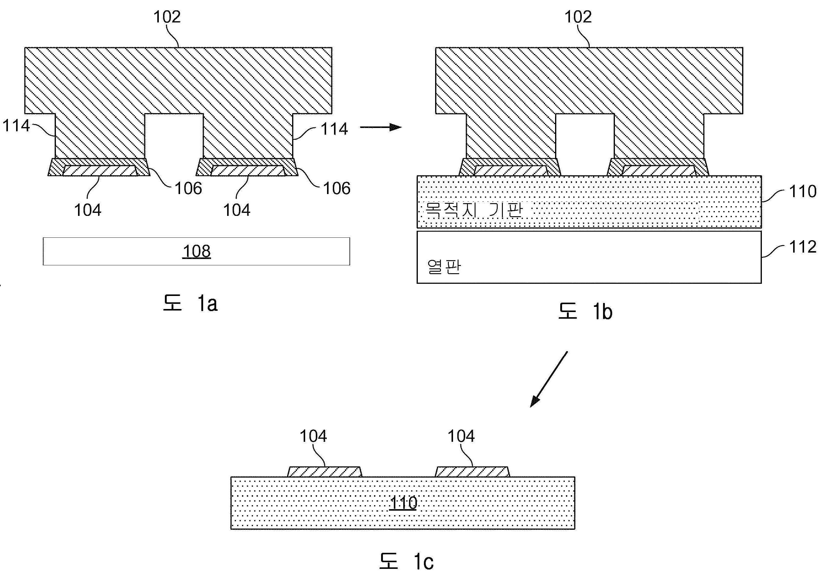
소정의 실시예들에서, 열-보조 마이크로-전사-인쇄가 비접착성 표면들 및 토포그래픽 표면들에 대해 수행된다. 폴리머 캡슐화부들은, 폴리머가 압축되도록 디자인될 때 비-네이티브 기판들에 반도체 디바이스들의 전사를 강화하고 그 다음으로 목적지 기판과 접촉하는 동안 리플로우하기 위하여 사용될 수 있다. 폴리머 층은 비-네이티브 기판 상에 전사된 디바이스 남겨 두면서 나중에 제거될 수 있다. 이것은 또한 토포그래픽 표면들로의 마이크로-전사-인쇄에 대한 능력을 개선시킨다.In certain embodiments, heat-assisted micro-transfer-printing is performed on non-adhesive surfaces and topographic surfaces. Polymer encapsulations can be used to enhance the transfer of semiconductor devices to non-native substrates when the polymer is designed to be compressed and then to reflow during contact with the destination substrate. The polymer layer can be removed later, leaving the device transferred onto the non-native substrate. This also improves the ability for micro-transfer-printing to topographic surfaces.
플라즈마 처리(예컨대, 진공이 요구되지 않음)는 마이크로 전사 인쇄 동안 수행될 수 있다. 플라즈마는 탄성중합체 전사-엘리먼트에 부착된 디바이스들의 하단 표면들에 적용될 수 있다. 하단 표면들의 이런 처리는 (i) 디바이스들과 목적지 기판 간의 개선된 본딩을 제공하고, (ii) 에피택셜 리프트-오프 방법들을 사용하여 제조되었던 디바이스들의 하단 표면을 세정하고, 그리고 (iii) 하단 표면으로부터 산화물들의 얇은 층들(예컨대, Cu-Cu, CuSn-Cu, Cu-Sn-Sn-Cu, Au-Au)을 제거(예컨대, 가스, 암모니아, 포름산 등을 형성하는 것과 같은 환원성 가스가 플라즈마에 부가되면)하기 위하여 사용될 수 있다. 처리는, 디바이스들이 분배되지 않는(예컨대, 스탬프를 떨어뜨리지 않음) 방식으로 디바이스들이 전사 디바이스 상에 있는 동안, 디바이스들에 적용될 수 있다.Plasma treatment (e.g., no vacuum is required) can be performed during micro transfer printing. Plasma can be applied to the bottom surfaces of devices attached to the elastomeric transfer-element. This treatment of the bottom surfaces (i) provides improved bonding between the devices and the destination substrate, (ii) cleans the bottom surface of the devices that were manufactured using epitaxial lift-off methods, and (iii) the bottom surface. Remove thin layers of oxides (e.g., Cu-Cu, CuSn-Cu, Cu-Sn-Sn-Cu, Au-Au) from (e.g., gas, ammonia, formic acid, etc.) Can be used to do). The processing can be applied to the devices while they are on the transfer device in a way that the devices are not dispensed (eg, do not drop a stamp).
소정의 실시예들에서, 플라즈마 처리는 전사 디바이스에 부착된 디바이스들의 하단 표면들에 적용될 수 있다. 처리는 디바이스들과 목적지 기판 간의 본딩을 개선하기 위하여 사용될 수 있다. 처리는 하단 표면들을 세정하고 및/또는 하단 표면들로부터 산화물들의 임의의 층들을 제거하기 위하여 사용될 수 있다. 디바이스들이 후면 금속을 가지면, 플라즈마는 금속의 표면으로부터 산화물들을 제거하기 위하여 사용될 수 있다.In certain embodiments, plasma treatment may be applied to the bottom surfaces of devices attached to the transfer device. The process can be used to improve the bonding between the devices and the destination substrate. The treatment can be used to clean the bottom surfaces and/or to remove any layers of oxides from the bottom surfaces. If the devices have a backside metal, plasma can be used to remove oxides from the surface of the metal.
소정의 실시예들에서, 디바이스들이 후면 금속을 가지면, 반도체 엘리먼트들은 플럭스로 코팅된 메이팅(mating) 금속 패드들을 가진 목적지 기판에 인쇄된다. 디바이스들을 전달한 후, 플럭스는 리플로우될 수 있고 이에 의해 패드들과 디바이스들 상의 후면 금속 간에 우수한 금속 연결이 남겨진다.In certain embodiments, if the devices have a backside metal, the semiconductor elements are printed on a destination substrate with mating metal pads coated with flux. After transferring the devices, the flux can be reflowed thereby leaving a good metal connection between the pads and the backside metal on the devices.
크라우닝(crowning) 효과는 종래 기술 방법들을 사용하여 제조된 전사 디바이스 벌크 재료의 에지에서 주목될 수 있다. 크라우닝은 예컨대 도 22에 도시된 바와 같이 벌크 재료와 하드-플레이트 인터페이스(예컨대, 유리) 간의 열 팽창 계수(CTE) 미스매칭에 의해 유발된다. 소정의 실시예들에서, 개시된 기술은 크라우닝에 관련된 문제들을 제거하거나 감소시키도록 디자인된 전사 디바이스들을 포함한다. 소정의 실시예들에서, 크라운은, 인쇄가능 반도체 엘리먼트들이 인쇄 동작 동안 크라운에 의해 픽업되지 않도록 면도기로 절단된다.The crowning effect can be noted at the edge of the transfer device bulk material manufactured using prior art methods. Crowning is caused, for example, by a coefficient of thermal expansion (CTE) mismatch between the bulk material and the hard-plate interface (eg, glass) as shown in FIG. 22. In certain embodiments, the disclosed technique includes transfer devices designed to eliminate or reduce problems related to crowning. In certain embodiments, the crown is cut with a razor such that printable semiconductor elements are not picked up by the crown during a printing operation.
소정의 실시예들에서, 제 2 재료는 벌크 볼륨과 하드-플레이트 인터페이스 간에 배치된다. 결과적으로, 제 2 재료 바로 위의 벌크 볼륨 재료는 그렇지 않은 경우보다 더 얇다. 이것은 크라운을 형성하기 위하여 재료가 더 적게 변형 및 블록해지기 때문에 더 작은 크라운을 형성한다. In certain embodiments, the second material is disposed between the bulk volume and the hard-plate interface. As a result, the bulk volume material directly above the second material is thinner than otherwise. This creates a smaller crown because less material is deformed and blocked to form the crown.
일부 실시예들에서, 벌크 볼륨의 베젤 또는 측벽은, 크라우닝이 최소화되도록 한다. 아래에 설명된 바와 같이, 소정의 형상의 측벽들은 더 적은 크라우닝을 가지는 전사 디바이스를 초래한다.In some embodiments, the bulk volume bezel or sidewall allows crowning to be minimized. As explained below, the sidewalls of a predetermined shape result in a transfer device with less crowning.
소정의 실시예들에서, 다수의 벌크 재료 층들(예컨대, 점탄성 재료)이 제공된다. 제 1 벌크 재료 층은 하드-플레이트 인터페이스 상에 있고, 통상적으로 보통 문제의 크라운인 것을 가진다. 제 2 벌크 재료 층은 제 1 벌크 재료 층 상에 제공된다. 제 2 벌크 재료 층은 제 1 벌크 재료 층보다 얇다. 제 2 벌크 재료 층이 더 얇아짐에 따라, 그것은 더 작은 크라운을 가질 것이다. 포스트들은 제 2 벌크 재료 층 상에 배치되고 벌크 재료의 제 2 층 상의 크라운에 비해 두드러진다. 부가적으로, 포스트들은 제 1 벌크 재료 층에 비해 두드러지는데, 그 이유는 제 2 벌크 재료 층의 두께 및 결합된 포스트들의 높이가 벌크 재료의 제 1 층 상의 크라운보다 더 크기 때문이다.In certain embodiments, multiple bulk material layers (eg, viscoelastic material) are provided. The first layer of bulk material is on the hard-plate interface and typically has what is the crown in question. A second bulk material layer is provided on the first bulk material layer. The second bulk material layer is thinner than the first bulk material layer. As the second bulk material layer gets thinner, it will have a smaller crown. The posts are disposed on the second layer of bulk material and stand out compared to the crown on the second layer of bulk material. Additionally, the posts stand out compared to the first layer of bulk material because the thickness of the second layer of bulk material and the height of the joined posts are greater than the crown on the first layer of bulk material.
소정의 실시예들에서, 전사 디바이스들은 포스트들의 연속적인 티어들 상에 연속적으로 더 작은 단면들을 가지는 다중-티어드 포스트들을 가진다. 마이크로-포스트는 포스트 상에 형성된다. 마이크로-포스트는 인쇄가능 반도체 디바이스들에 물리적으로 접촉하기 위하여 사용된다. 마이크로-포스트는 통상적으로 포스트보다 더 짧고 더 좁다. 다중-티어드 포스트들의 사용은 여전히 작은 디바이스들이 픽업되게 하면서 포스트들에 대해 원하는 종횡비들이 유지되게 한다. 다중-티어드 포스트에 의해 얻어진 높이는 포스트의 높이가 증가됨에 따라 크라우닝 문제들의 위험을 감소시킬 수 있다. 부가적으로, 다중-티어드 포스트들은 새깅(sagging)에 관련된 문제들을 감소시킬 수 있다.In certain embodiments, transfer devices have multi-tiered posts with continuously smaller cross sections on successive tiers of the posts. The micro-post is formed on the post. Micro-posts are used to physically contact printable semiconductor devices. Micro-posts are typically shorter and narrower than posts. The use of multi-tiered posts allows the desired aspect ratios to be maintained for the posts while still allowing small devices to be picked up. The height obtained by the multi-tiered post can reduce the risk of crowning problems as the height of the post increases. Additionally, multi-tiered posts can reduce problems related to sagging.
전사 디바이스가 픽업 동작 동안 압축될 때, 포스트들 간의 새깅 가능성이 있다. 이런 새그는 소스 기판으로부터 원하지 않은 재료들이 픽업되게 한다. 인접한 포스트들 사이의 경간(span)이 증가됨에 따라, 문제들을 유발하는 새그의 위험은 증가한다.When the transfer device is compressed during the pickup operation, there is a possibility of sagging between the posts. This sag causes unwanted materials to be picked up from the source substrate. As the span between adjacent posts increases, the risk of sags causing problems increases.
다중-티어드 포스트들은 포스트들에 대해 원하는 종횡비들을 유지하면서 포스트들의 높이를 증가시키기 위하여 사용될 수 있고, 따라서 새깅 및 크라우닝에 관련된 문제들이 감소된다. 소정의 실시예들에서, 새그-방지 특징들은 전사 디바이스 상의 포스트들 간에 제공된다. 새그-방지 특징들은, 그들이 디바이스들이 픽업을 하지 못하도록 하는 종횡비를 가질 수 있다. 이런 방식으로, 새그-방지 포스트들은 전사 디바이스의 벌크 재료의 보디가 소스 기판에 접촉하는 것을 방지하고, 이에 의해 새깅에 관련된 문제들을 감소시킨다.Multi-tiered posts can be used to increase the height of the posts while maintaining the desired aspect ratios for the posts, thus reducing problems related to sagging and crowning. In certain embodiments, anti-sag features are provided between the posts on the transfer device. Anti-sag features can have an aspect ratio that prevents devices from picking up. In this way, the anti-sag posts prevent the body of the bulk material of the transfer device from contacting the source substrate, thereby reducing problems related to sagging.
소정의 실시예들에서, 전사 디바이스에는 포스트들 간에 거친 표면이 제공된다. 거친 표면은, 거친 표면이 접착을 감소시키기 때문에 새깅이 발생하면 인쇄가능 반도체 엘리먼트들이 픽업될 위험을 감소시킨다.In certain embodiments, the transfer device is provided with a rough surface between the posts. The rough surface reduces the risk of picking up printable semiconductor elements if sagging occurs because the rough surface reduces adhesion.
일 양상에서, 본 개시된 기술은 목적지 기판의 수신 표면 상에 반도체 디바이스를 어셈블링하기 위한 방법을 포함하고, 방법은 네이티브 기판 상에 형성되는 반도체 디바이스를 제공하는 단계; 접촉 표면을 갖는 등각 전사 디바이스와 반도체 디바이스의 상단 표면을 접촉시키는 단계 ― 접촉 표면과 반도체 디바이스의 상단 표면 간의 접촉은 반도체 디바이스를 등각 전사 디바이스에 적어도 일시적으로 바인딩(bind)함 ―; 반도체 디바이스가 네이티브 기판으로부터 탈착되는 경우에 등각 전사 디바이스의 접촉 표면이 그 위에 배치되는 반도체 디바이스를 갖도록, 반도체 디바이스를 네이티브 기판으로부터 분리하는 단계; 반도체 디바이스를 목적지 기판의 수신 표면과 접촉시키기 이전에, 네이티브 기판으로부터의 분리에 이어서 반도체 디바이스의 후면 표면을 플라즈마(예컨대, 대기압 플라즈마)에 노출시키는 단계; 접촉 표면 상에 배치되는 반도체 디바이스를 목적지 기판의 수신 표면과 접촉시키는 단계; 및 목적지 기판의 수신 표면 상에 반도체 디바이스를 어셈블링하기 위해서, 등각 전사 디바이스의 접촉 표면을 반도체 디바이스로부터 분리하는 단계를 포함한다.In one aspect, the disclosed technology includes a method for assembling a semiconductor device on a receiving surface of a destination substrate, the method comprising: providing a semiconductor device formed on a native substrate; Contacting a top surface of the semiconductor device with a conformal transfer device having a contact surface, the contact between the contact surface and the top surface of the semiconductor device at least temporarily binding the semiconductor device to the conformal transfer device; Separating the semiconductor device from the native substrate so that when the semiconductor device is detached from the native substrate, the contact surface of the conformal transfer device has the semiconductor device disposed thereon; Exposing the back surface of the semiconductor device to a plasma (eg, atmospheric plasma) following separation from the native substrate prior to contacting the semiconductor device with the receiving surface of the destination substrate; Contacting a semiconductor device disposed on the contact surface with a receiving surface of the destination substrate; And separating the contact surface of the conformal transfer device from the semiconductor device to assemble the semiconductor device on the receiving surface of the destination substrate.
소정의 실시예들에서, 후면 표면을 플라즈마에 노출시키는 단계는 반도체 디바이스와 목적지 기판의 수신 표면 간의 본딩(bonding)을 개선시킨다.In certain embodiments, exposing the back surface to the plasma improves bonding between the semiconductor device and the receiving surface of the destination substrate.
소정의 실시예들에서, 후면 표면을 플라즈마에 노출시키는 단계는 반도체 디바이스의 후면 표면을 세정한다. In certain embodiments, exposing the back surface to a plasma cleans the back surface of the semiconductor device.
소정의 실시예들에서, 후면 표면을 플라즈마에 노출시키는 단계는 반도체 디바이스의 후면 표면으로부터 산화물들의 얇은 층들을 제거한다. In certain embodiments, exposing the back surface to the plasma removes thin layers of oxides from the back surface of the semiconductor device.
소정의 실시예들에서, 목적지 기판은 폴리머, 플라스틱, 수지, 폴리이미드, PEN, PET, 금속, 금속 포일, 유리, 반도체 및 사파이어로 구성되는 그룹으로부터 선택되는 부재이다.In certain embodiments, the destination substrate is a member selected from the group consisting of polymer, plastic, resin, polyimide, PEN, PET, metal, metal foil, glass, semiconductor, and sapphire.
소정의 실시예들에서, 목적지 기판은 가시 광에 대해 50%, 80%, 90%, 또는 95% 보다 크거나 동일한 투명성을 갖는다.In certain embodiments, the destination substrate has greater than or equal to 50%, 80%, 90%, or 95% transparency for visible light.
소정의 실시예들에서, 네이티브 기판은 무기 반도체 재료, 단결정 실리콘 웨이퍼들, 실리콘 온 절연체 웨이퍼들, 다결정 실리콘 웨이퍼들, GaAs 웨이퍼들, Si(1 1 1), InAlP, InP, GaAs, InGaAs, AlGaAs, GaSb, GaAlSb, AlSb, InSb, InGaAlSbAs, InAlSb, 및 InGaP로 구성되는 그룹으로부터 선택되는 부재를 포함한다. In certain embodiments, the native substrate is an inorganic semiconductor material, single crystal silicon wafers, silicon on insulator wafers, polycrystalline silicon wafers, GaAs wafers, Si(1 1 1), InAlP, InP, GaAs, InGaAs, AlGaAs , GaSb, GaAlSb, AlSb, InSb, InGaAlSbAs, InAlSb, and a member selected from the group consisting of InGaP.
소정의 실시예들에서, 플라즈마는 환원성 가스를 포함한다. In certain embodiments, the plasma comprises a reducing gas.
소정의 실시예들에서, 방법은, 등각 전사 디바이스의 접촉 표면으로부터 반도체 디바이스들의 전단(shearing) 및 박리(delamination)를 방지하기 위해서, 듀티 사이클, 체류 시간, 플라즈마의 전력, 및 반도체 디바이스까지의 플라즈마의 거리 중 적어도 하나를 제어하는 단계를 포함한다.In certain embodiments, the method includes the duty cycle, residence time, power of the plasma, and plasma to the semiconductor device to prevent shearing and delamination of semiconductor devices from the contact surface of the conformal transfer device. And controlling at least one of the distances.
소정의 실시예들에서, 반도체 디바이스의 후면 표면은 금속을 포함한다. In certain embodiments, the back surface of the semiconductor device comprises a metal.
소정의 실시예들에서, 금속은 구리, 주석, 알루미늄 및 이들의 혼합물 중 적어도 하나이다. In certain embodiments, the metal is at least one of copper, tin, aluminum, and mixtures thereof.
소정의 실시예들에서, 목적지 기판의 수신 표면은 적어도 부분적으로 금속을 포함한다. In certain embodiments, the receiving surface of the destination substrate at least partially comprises metal.
소정의 실시예들에서, 금속은 구리, 주석, 알루미늄 및 이들의 혼합물 중 적어도 하나이다. In certain embodiments, the metal is at least one of copper, tin, aluminum, and mixtures thereof.
소정의 실시예들에서, 등각 전사 디바이스는 점탄성 스탬프 및 탄성 스탬프 중 적어도 하나를 포함한다. In certain embodiments, the conformal transfer device includes at least one of a viscoelastic stamp and an elastic stamp.
소정의 실시예들에서, 방법은 접촉 표면 상에 배치되는 반도체 디바이스를 목적지 기판의 수신 표면과 접촉시키기 이전에, 네이티브 기판으로부터 반도체 디바이스를 픽업하기 위해서 등각 전사 디바이스를 네이티브 기판으로부터 분리하는 단계를 포함한다. In certain embodiments, the method includes separating the conformal transfer device from the native substrate to pick up the semiconductor device from the native substrate prior to contacting the semiconductor device disposed on the contact surface with the receiving surface of the destination substrate. do.
소정의 실시예들에서, 등각 전사 디바이스를 네이티브 기판으로부터 분리하는 단계는 5g 이상(예컨대, 5-100g)의 초기 가속도로 수행된다. In certain embodiments, the step of separating the conformal transfer device from the native substrate is performed with an initial acceleration of 5 g or more (eg, 5-100 g).
소정의 실시예들에서, 등각 전사 디바이스를 네이티브 기판으로부터 분리하는 단계는, (i) 등각 전사 디바이스를 네이티브 기판으로부터 멀리 이동시키는 단계; 및 (ii) 네이티브 기판을 등각 전사 디바이스로부터 멀리 이동시키는 단계 중 하나 또는 둘 모두를 포함한다. In certain embodiments, separating the conformal transfer device from the native substrate comprises: (i) moving the conformal transfer device away from the native substrate; And (ii) moving the native substrate away from the conformal transfer device.
소정의 실시예들에서, 등각 전사 디바이스는 원통형 포스트, 삼각형 포스트, 직사각형 포스트, 오각형 포스트, 육각형 포스트, 칠각형 포스트 및 팔각형 포스트 중 적어도 하나를 포함한다. In certain embodiments, the conformal transfer device includes at least one of a cylindrical post, a triangular post, a rectangular post, a pentagonal post, a hexagonal post, a heptagonal post, and an octagonal post.
소정의 실시예들에서, 목적지 기판의 수신 표면 상에 반도체 디바이스들의 어레이를 어셈블링하기 위해서, 등각 전사 디바이스는 네이티브 기판 상의 개별 반도체 디바이스와 접촉하도록 각각 성형된 복수의 포스트들을 가진 전사 디바이스 층을 포함한다. In certain embodiments, to assemble an array of semiconductor devices on a receiving surface of a destination substrate, the conformal transfer device includes a transfer device layer having a plurality of posts each shaped to contact a respective semiconductor device on the native substrate. do.
소정의 실시예들에서, 등각 전사 디바이스는 복수의 포스트들 중 두 개의 인접한 포스트들 간에 위치되는 하나 또는 그 초과의 새그-방지 포스트들을 포함한다. In certain embodiments, the conformal transfer device includes one or more anti-sag posts positioned between two adjacent ones of the plurality of posts.
소정의 실시예들에서, 새그-방지 포스트들은 포스트들 중 하나 또는 그 초과의 포스트의 높이보다 작은 높이를 갖는다. In certain embodiments, the anti-sag posts have a height less than the height of one or more of the posts.
소정의 실시예들에서, 복수의 포스트들의 각각의 포스트 간의 전사 디바이스의 표면은 거친 표면이다. In certain embodiments, the surface of the transfer device between each post of the plurality of posts is a rough surface.
소정의 실시예들에서, 전사 디바이스의 벌크 볼륨은 제 1 재료를 포함하고, 복수의 포스트들은 제 2 재료를 포함하며, 복수의 포스트들은 벌크 볼륨 상에 배치된다. In certain embodiments, the bulk volume of the transfer device comprises a first material, a plurality of posts comprises a second material, and the plurality of posts is disposed on the bulk volume.
소정의 실시예들에서, 방법은 접촉 표면 상에 배치되는 반도체 디바이스를 목적지 기판의 수신 표면과 접촉시킨 이후에, 가열 엘리먼트에 의해서 폴리머 층을 가열하는 단계를 포함한다. In certain embodiments, the method includes heating the polymer layer by means of a heating element after contacting the semiconductor device disposed on the contact surface with the receiving surface of the destination substrate.
소정의 실시예들에서, 방법은 네이티브 기판 상에 형성된 반도체 디바이스를 제공한 이후에, 반도체 디바이스와 네이티브 기판 간에 형성되는 탈착 층의 적어도 일부를 에칭하는 단계를 포함한다. In certain embodiments, the method includes, after providing the semiconductor device formed on the native substrate, etching at least a portion of the detachment layer formed between the semiconductor device and the native substrate.
소정의 실시예들에서, 반도체 디바이스는 유니터리(unitary) 무기 반도체 구조를 포함한다. In certain embodiments, the semiconductor device comprises a unitary inorganic semiconductor structure.
소정의 실시예들에서, 목적지 기판은 Si를 포함한다. In certain embodiments, the destination substrate comprises Si.
소정의 실시예들에서, 반도체 디바이스는 캡슐화 폴리머 층을 포함한다.In certain embodiments, the semiconductor device includes an encapsulating polymer layer.
소정의 실시예들에서, 등각 전사 디바이스는 복수의 포스트들과 동일한 높이의 하나 또는 그 초과의 새그-방지 포스트들을 포함하고, 각각의 새그-방지 포스트는 복수의 포스트들 중 적어도 두 개의 포스트들 간에 위치된다. In certain embodiments, the conformal transfer device comprises one or more anti-sag posts of the same height as the plurality of posts, each anti-sag post between at least two of the plurality of posts. Is located.
소정의 실시예들에서, 반도체 디바이스의 금속 후면 표면이 목적지 기판 상의 플럭스 층에 적어도 부분적으로 접촉하도록, 반도체 디바이스는 목적지 기판의 수신 표면 상에 어셈블링된다. In certain embodiments, the semiconductor device is assembled on the receiving surface of the destination substrate such that the metal back surface of the semiconductor device at least partially contacts the flux layer on the destination substrate.
소정의 실시예들에서, 방법은 목적지 기판의 수신 표면 상에 반도체 디바이스를 어셈블링한 이후에, 금속 후면 표면을 금속 패드에 고정하기 위해서 플럭스 층을 열적으로 처리하는 단계를 포함한다. In certain embodiments, the method includes, after assembling the semiconductor device on the receiving surface of the destination substrate, thermally treating the flux layer to secure the metal back surface to the metal pad.
소정의 실시예들에서, 반도체 디바이스는 반도체 디바이스의 상단 표면 상에 배치되는 폴리머 층을 갖는다. In certain embodiments, the semiconductor device has a polymer layer disposed on the top surface of the semiconductor device.
다른 양상에서, 개시된 기술은 목적지 기판의 수신 표면 상에 반도체 디바이스를 어셈블링하기 위한 방법을 포함하며, 방법은 네이티브 기판 상에 형성되는 반도체 디바이스를 제공하는 단계 ― 반도체 디바이스의 상단 표면 상에 폴리머 층이 배치됨 ―; 접촉 표면을 갖는 등각 전사 디바이스와 반도체 디바이스의 폴리머 층을 접촉시키는 단계 ― 접촉 표면과 반도체 디바이스 간의 접촉은 반도체 디바이스를 등각 전사 디바이스에 적어도 일시적으로 바인딩함 ―; 반도체 디바이스가 등각 전사 디바이스의 접촉 표면 상에 배치되고 네이티브 기판으로부터 탈착되도록, 반도체 디바이스를 네이티브 기판으로부터 분리하는 단계; 접촉 표면 상에 배치되는 반도체 디바이스를 목적지 기판의 수신 표면에 접촉시키는 단계; 가열 엘리먼트에 의해서 폴리머 층을 가열하는 단계; 및 목적지 기판의 수신 표면 상에 반도체 디바이스를 어셈블링하기 위해서, 반도체 디바이스가 수신 표면 상에 전사되도록 등각 전사 디바이스의 접촉 표면을 반도체 디바이스로부터 분리하는 단계를 포함한다. In another aspect, the disclosed technique includes a method for assembling a semiconductor device on a receiving surface of a destination substrate, the method comprising providing a semiconductor device formed on a native substrate-a polymer layer on a top surface of the semiconductor device. Is placed -; Contacting the polymer layer of the semiconductor device with a conformal transfer device having a contact surface, the contact between the contact surface and the semiconductor device at least temporarily binding the semiconductor device to the conformal transfer device; Separating the semiconductor device from the native substrate such that the semiconductor device is disposed on the contact surface of the conformal transfer device and detached from the native substrate; Contacting the semiconductor device disposed on the contact surface with the receiving surface of the destination substrate; Heating the polymer layer by means of a heating element; And separating the contact surface of the conformal transfer device from the semiconductor device such that the semiconductor device is transferred onto the receiving surface to assemble the semiconductor device on the receiving surface of the destination substrate.
소정의 실시예들에서, 가열 엘리먼트는 열판이다. In certain embodiments, the heating element is a hot plate.
소정의 실시예들에서, 가열 엘리먼트는 반도체 디바이스에 대향하는 목적지 기판의 측면 상에 배치된다. In certain embodiments, the heating element is disposed on the side of the destination substrate opposite the semiconductor device.
소정의 실시예들에서, 목적지 기판은 반도체 디바이스들에 대해 비-네이티브적이다. In certain embodiments, the destination substrate is non-native for semiconductor devices.
소정의 실시예들에서, 상기 방법은, 폴리머 층을 가열한 이후에, 폴리머를 적어도 부분적으로 제거하는 단계를 포함한다. In certain embodiments, the method includes, after heating the polymer layer, at least partially removing the polymer.
소정의 실시예들에서, 가열 엘리먼트로부터의 열은 폴리머 층의 점성을 감소시키고, 폴리머 층으로 하여금 유동하게 한다.In certain embodiments, heat from the heating element reduces the viscosity of the polymer layer and causes the polymer layer to flow.
소정의 실시예들에서, 폴리머 층은 반도체 디바이스의 상단 표면 및 반도체 디바이스의 하나 또는 그 초과의 측면들 상에 배치된다. In certain embodiments, the polymer layer is disposed on the top surface of the semiconductor device and on one or more sides of the semiconductor device.
소정의 실시예들에서, 폴리머 층은 인쇄가능 반도체의 적어도 일부를 네이티브 기판 상에 캡슐화한다. In certain embodiments, the polymer layer encapsulates at least a portion of the printable semiconductor on the native substrate.
소정의 실시예들에서, 목적지 기판의 수신 표면은 비-평면 토포그래피컬 표면을 포함한다. In certain embodiments, the receiving surface of the destination substrate comprises a non-planar topographical surface.
소정의 실시예들에서, 목적지 기판은 폴리머, 플라스틱, 수지, 폴리이미드, PEN, PET, 금속, 금속 포일, 유리, 반도체 및 사파이어로 구성되는 그룹으로부터 선택되는 부재이다. In certain embodiments, the destination substrate is a member selected from the group consisting of polymer, plastic, resin, polyimide, PEN, PET, metal, metal foil, glass, semiconductor, and sapphire.
소정의 실시예들에서, 목적지 기판은 가시 광에 대해 50%, 80%, 90%, 또는 95% 보다 크거나 동일한 투명성을 갖는다. In certain embodiments, the destination substrate has greater than or equal to 50%, 80%, 90%, or 95% transparency for visible light.
소정의 실시예들에서, 네이티브 기판은 무기 반도체 재료, 단결정 실리콘 웨이퍼들, 실리콘 온 절연체 웨이퍼들, 다결정 실리콘 웨이퍼들, GaAs 웨이퍼들, Si(1 1 1), InAlP, InP, GaAs, InGaAs, AlGaAs, GaSb, GaAlSb, AlSb, InSb, InGaAlSbAs, InAlSb, 및 InGaP로 구성되는 그룹으로부터 선택되는 부재를 포함한다. In certain embodiments, the native substrate is an inorganic semiconductor material, single crystal silicon wafers, silicon on insulator wafers, polycrystalline silicon wafers, GaAs wafers, Si(1 1 1), InAlP, InP, GaAs, InGaAs, AlGaAs , GaSb, GaAlSb, AlSb, InSb, InGaAlSbAs, InAlSb, and a member selected from the group consisting of InGaP.
소정의 실시예들에서, 반도체 디바이스의 금속 후면 표면이 목적지 기판 상의 플럭스 층에 적어도 부분적으로 접촉하도록, 반도체 디바이스는 목적지 기판의 수신 표면 상에 어셈블링된다. In certain embodiments, the semiconductor device is assembled on the receiving surface of the destination substrate such that the metal back surface of the semiconductor device at least partially contacts the flux layer on the destination substrate.
소정의 실시예들에서, 방법은 목적지 기판의 수신 표면 상에 반도체 디바이스를 어셈블링한 이후에, 금속 후면 표면을 금속 패드에 고정하기 위해서 플럭스 층을 열적으로 처리하는 단계를 포함한다. In certain embodiments, the method includes, after assembling the semiconductor device on the receiving surface of the destination substrate, thermally treating the flux layer to secure the metal back surface to the metal pad.
소정의 실시예들에서, 방법은 반도체 디바이스를 목적지 기판의 수신 표면과 접촉시키기 이전에, 반도체 디바이스의 상단 표면에 대향하는 반도체 디바이스의 후면 표면을 네이티브 기판으로부터의 분리에 이어서 플라즈마에 노출시키는 단계를 포함한다. In certain embodiments, the method includes, prior to contacting the semiconductor device with the receiving surface of the destination substrate, exposing the back surface of the semiconductor device opposite the top surface of the semiconductor device to the plasma following separation from the native substrate. Include.
다른 양상에서, 개시되는 기술은 목적지 기판의 수신 표면 상에 반도체 디바이스를 어셈블링하기 위한 방법을 포함하며, 방법은 네이티브 기판 상에 형성되는 반도체 디바이스를 제공하는 단계 ― 반도체 디바이스는 금속 후면 표면을 포함함 ―; 접촉 표면을 갖는 등각 전사 디바이스와 반도체 디바이스의 상단 표면을 접촉시키는 단계 ― 접촉 표면과 반도체 디바이스 간의 접촉은 반도체 디바이스를 등각 전사 디바이스에 적어도 일시적으로 바인딩함 ―; 반도체 디바이스가 네이티브 기판으로부터 탈착되는 경우에 등각 전사 디바이스의 접촉 표면이 그 위에 배치되는 반도체 디바이스를 갖도록, 반도체 디바이스를 네이티브 기판으로부터 분리하는 단계; 접촉 표면 상에 배치되는 반도체 디바이스를 목적지 기판의 수신 표면과 접촉시키는 단계 ― 수신 표면은 목적지 기판 상에 배치되는 금속 패드 상의 플럭스 층을 포함함 ―; 반도체 디바이스의 금속 후면 표면이 플럭스 층에 적어도 부분적으로 접촉하도록 목적지 기판의 수신 표면 상에 반도체 디바이스를 어셈블링하기 위해서, 등각 전사 디바이스의 접촉 표면을 반도체 디바이스로부터 분리하는 단계; 및 금속 후면 표면을 금속 패드에 고정하기 위해서 플럭스 층을 열에 노출시키는 단계를 포함한다. In another aspect, the disclosed technique includes a method for assembling a semiconductor device on a receiving surface of a destination substrate, the method comprising providing a semiconductor device formed on a native substrate, the semiconductor device comprising a metal back surface. Ham -; Contacting a top surface of the semiconductor device with a conformal transfer device having a contact surface, the contact between the contact surface and the semiconductor device at least temporarily binding the semiconductor device to the conformal transfer device; Separating the semiconductor device from the native substrate so that when the semiconductor device is detached from the native substrate, the contact surface of the conformal transfer device has the semiconductor device disposed thereon; Contacting a semiconductor device disposed on the contact surface with a receiving surface of the destination substrate, the receiving surface comprising a layer of flux on a metal pad disposed on the destination substrate; Separating the contact surface of the conformal transfer device from the semiconductor device to assemble the semiconductor device on the receiving surface of the destination substrate such that the metal back surface of the semiconductor device at least partially contacts the flux layer; And exposing the flux layer to heat to secure the metal back surface to the metal pad.
소정의 실시예들에서, 플럭스 층을 열적으로 처리하는 것은 플럭스 층을 열에 노출시키는 것을 포함한다. In certain embodiments, thermally treating the flux layer includes exposing the flux layer to heat.
소정의 실시예들에서, 플럭스 층은 가열 엘리먼트를 사용하여 열에 노출된다. In certain embodiments, the flux layer is exposed to heat using a heating element.
소정의 실시예들에서, 가열 엘리먼트는 열판이다. In certain embodiments, the heating element is a hot plate.
소정의 실시예들에서, 가열 엘리먼트는 인쇄가능 반도체 디바이스에 대향하는 목적지 기판의 측면 상에 배치된다. In certain embodiments, the heating element is disposed on the side of the destination substrate opposite the printable semiconductor device.
소정의 실시예들에서, 네이티브 기판 상에 형성되는 반도체 디바이스를 제공하는 단계는 네이티브 기판 상에 형성되는 반도체 디바이스를 제공하는 단계를 포함하며, 반도체 디바이스의 상단 표면 상에 폴리머 층이 배치된다. In certain embodiments, providing a semiconductor device formed on a native substrate includes providing a semiconductor device formed on the native substrate, with a polymer layer disposed on a top surface of the semiconductor device.
소정의 실시예들에서, 목적지 기판은 폴리머, 플라스틱, 수지, 폴리이미드, PEN, PET, 금속, 금속 포일, 유리, 반도체 및 사파이어로 구성되는 그룹으로부터 선택되는 부재이다. In certain embodiments, the destination substrate is a member selected from the group consisting of polymer, plastic, resin, polyimide, PEN, PET, metal, metal foil, glass, semiconductor, and sapphire.
소정의 실시예들에서, 목적지 기판은 가시 광에 대해 50%, 80%, 90%, 또는 95% 보다 크거나 동일한 투명성을 갖는다. In certain embodiments, the destination substrate has greater than or equal to 50%, 80%, 90%, or 95% transparency for visible light.
소정의 실시예들에서, 네이티브 기판은 무기 반도체 재료, 단결정 실리콘 웨이퍼들, 실리콘 온 절연체 웨이퍼들, 다결정 실리콘 웨이퍼들, GaAs 웨이퍼들, Si(1 1 1), InAlP, InP, GaAs, InGaAs, AlGaAs, GaSb, GaAlSb, AlSb, InSb, InGaAlSbAs, InAlSb, 및 InGaP로 구성되는 그룹으로부터 선택되는 부재를 포함한다. In certain embodiments, the native substrate is an inorganic semiconductor material, single crystal silicon wafers, silicon on insulator wafers, polycrystalline silicon wafers, GaAs wafers, Si(1 1 1), InAlP, InP, GaAs, InGaAs, AlGaAs , GaSb, GaAlSb, AlSb, InSb, InGaAlSbAs, InAlSb, and a member selected from the group consisting of InGaP.
소정의 실시예들에서, 네이티브 기판 상에 형성되는 반도체 디바이스를 제공하는 단계는 네이티브 기판 상에 반도체 디바이스를 형성하는 단계; 및 인쇄가능 반도체를 적어도 부분적으로 폴리머 층과 함께 캡슐화하는 단계를 포함한다. In certain embodiments, providing a semiconductor device formed on a native substrate includes forming a semiconductor device on the native substrate; And encapsulating the printable semiconductor at least partially with the polymer layer.
소정의 실시예들에서, 네이티브 기판 상에 형성되는 반도체 디바이스는 폴리머 층과 함께 캡슐화된다. In certain embodiments, a semiconductor device formed on a native substrate is encapsulated with a polymer layer.
소정의 실시예들에서, 목적지 기판의 수신 표면은 하나 또는 그 초과의 비-평면 토포그래피컬 특징들을 포함한다. In certain embodiments, the receiving surface of the destination substrate includes one or more non-planar topographical features.
소정의 실시예들에서, 하나 또는 그 초과의 비-평면 토포그래피컬 특징들은 메사들, v-형상 채널들 및 트렌치들로 구성되는 그룹으로부터 선택되는 적어도 하나의 부재를 포함한다. In certain embodiments, the one or more non-planar topographical features include at least one member selected from the group consisting of mesas, v-shaped channels and trenches.
소정의 실시예들에서, 반도체 디바이스는 반도체 디바이스의 상단 표면 상에 배치되는 폴리머 층을 갖는다. In certain embodiments, the semiconductor device has a polymer layer disposed on the top surface of the semiconductor device.
소정의 실시예들에서, 방법은 접촉 표면 상에 배치되는 반도체 디바이스를 목적지 기판의 수신 표면과 접촉시킨 이후에, 가열 엘리먼트에 의해서 폴리머 층을 가열하는 단계를 포함한다. In certain embodiments, the method includes heating the polymer layer by means of a heating element after contacting the semiconductor device disposed on the contact surface with the receiving surface of the destination substrate.
소정의 실시예들에서, 방법은 네이티브 기판으로부터의 분리에 이어서 그리고 반도체 디바이스를 목적지 기판의 수신 표면과 접촉시키기 이전에, 반도체 디바이스의 상단 표면에 대향하는 반도체 디바이스의 후면 표면을 플라즈마에 노출시키는 단계를 포함한다. In certain embodiments, the method further comprises exposing a back surface of the semiconductor device opposite the top surface of the semiconductor device to a plasma following separation from the native substrate and prior to contacting the semiconductor device with the receiving surface of the destination substrate. Includes.
다른 양상에서, 개시되는 기술은 감소된 크라우닝을 갖는 등각 전사 디바이스를 포함하며, 전사 디바이스는 제 1 표면 및 제 1 표면에 대향하는 제 2 표면, 및 제 1 표면과 제 2 표면 간의 측면을 갖는 벌크 볼륨 ― 벌크 볼륨은 측면을 제 1 표면에 연결하는 테이퍼링된 표면을 포함함 ―; 및 인쇄가능 재료를 픽업하기 위해 벌크 볼륨의 제 1 표면 상에 배치되는 복수의 인쇄 포스트들을 포함하고, 복수의 인쇄 포스트들 및 벌크 볼륨은 벌크 볼륨의 제 2 표면에 적용되는 힘이 복수의 인쇄 포스트들에 전송되도록 배열된다. In another aspect, the disclosed technology includes a conformal transfer device with reduced crowning, the transfer device having a first surface and a second surface opposite the first surface, and a side surface between the first surface and the second surface. Bulk volume, the bulk volume comprising a tapered surface connecting the side surface to the first surface; And a plurality of print posts disposed on the first surface of the bulk volume to pick up the printable material, wherein the plurality of print posts and the bulk volume are applied to the second surface of the bulk volume by a force applied to the plurality of print posts. Arranged to be transmitted to the field.
소정의 실시예들에서, 복수의 포스트들의 각각의 포스트의 종횡비(높이-대-폭)는 4:1보다 작거나 동일하다(예컨대, 2:1 내지 4:1). In certain embodiments, the aspect ratio (height-to-width) of each post of the plurality of posts is less than or equal to 4:1 (eg, 2:1 to 4:1).
소정의 실시예들에서, 복수의 인쇄 포스트들의 각각의 포스트는 제 1 표면에 대향하는 포스트의 단부 상에 접촉 표면을 포함하고, 복수의 포스트들의 접촉 표면들은 실질적으로 동일 평면에 있다. In certain embodiments, each post of the plurality of printing posts includes a contact surface on an end of the post opposite the first surface, the contact surfaces of the plurality of posts being substantially coplanar.
소정의 실시예들에서, 복수의 인쇄 포스트들의 두께는 1 미크론 내지 100 미크론(예컨대, 1 내지 5 미크론, 5 내지 10 미크론, 10 내지 15 미크론, 50 내지 25 미크론, 25 내지 40 미크론, 40 내지 60 미크론, 60 내지 80 미크론, 또는 80 내지 100 미크론)이다. In certain embodiments, the thickness of the plurality of printing posts is 1 micron to 100 microns (e.g., 1 to 5 microns, 5 to 10 microns, 10 to 15 microns, 50 to 25 microns, 25 to 40 microns, 40 to 60 microns). Microns, 60 to 80 microns, or 80 to 100 microns).
소정의 실시예들에서, 벌크 볼륨의 두께는 0.5 mm 내지 5 mm(예컨대, 0.5 내지 1 mm, 1 내지 2 mm, 2 내지 3 mm, 3 내지 4 mm, 또는 4 내지 5 mm)이다.In certain embodiments, the thickness of the bulk volume is 0.5 mm to 5 mm (eg, 0.5 to 1 mm, 1 to 2 mm, 2 to 3 mm, 3 to 4 mm, or 4 to 5 mm).
소정의 실시예들에서, 복수의 인쇄 포스트들의 두께와 벌크 볼륨의 두께의 비율은 1:1 내지 1:10(예컨대, 1:1 내지 1:2, 1:2 내지 1:4, 1:4 내지 1:6, 1:6 내지 1:8, 또는 1:8 내지 1:10)이다. In certain embodiments, the ratio of the thickness of the plurality of printing posts to the thickness of the bulk volume is 1:1 to 1:10 (e.g., 1:1 to 1:2, 1:2 to 1:4, 1:4 To 1:6, 1:6 to 1:8, or 1:8 to 1:10).
소정의 실시예들에서, 벌크 볼륨은 1 GPa 내지 10 GPa(예컨대, 1 내지 4 GPa, 4 내지 7 GPa, 7 내지 10 GPa)의 영률을 갖는다. In certain embodiments, the bulk volume has a Young's modulus of 1 GPa to 10 GPa (eg, 1 to 4 GPa, 4 to 7 GPa, 7 to 10 GPa).
소정의 실시예들에서, 복수의 인쇄 포스트들은 1 MPa 내지 10 MPa(예컨대, 1 내지 4 MPa, 4 내지 7 MPa, 7 내지 10 MPa)의 영률을 갖는다. In certain embodiments, the plurality of print posts have a Young's modulus of 1 MPa to 10 MPa (eg, 1 to 4 MPa, 4 to 7 MPa, 7 to 10 MPa).
소정의 실시예들에서, 복수의 인쇄 포스트들은 제 1 영률을 갖고, 기저부는 제 1 영률보다 큰 제 2 영률을 갖는다. In certain embodiments, the plurality of printing posts have a first Young's modulus, and the base portion has a second Young's modulus that is greater than the first Young's modulus.
소정의 실시예들에서, 벌크 볼륨은 14.5 ppm보다 작거나 동일한 열 팽창 계수를 갖는 폴리머를 포함한다. In certain embodiments, the bulk volume comprises a polymer having a coefficient of thermal expansion less than or equal to 14.5 ppm.
소정의 실시예들에서, 복수의 인쇄 포스트들은 10 cm2 내지 260 cm2(예컨대, 10 cm2 내지 40 cm2, 40 cm2 내지 80 cm2, 120 cm2 내지 160 cm2, 160 cm2 내지 200 cm2, 200 cm2 내지 240 cm2, 또는 240 cm2 내지 260 cm2)의 선택되는 영역을 점유한다. In certain embodiments, the plurality of printing posts are 10 cm 2 to 260 cm 2 (eg, 10 cm 2 to 40 cm 2 , 40 cm 2 to 80 cm 2 , 120 cm 2 to 160 cm 2 , 160 cm 2 to 200 cm 2 , 200 cm 2 to 240 cm 2 , or 240 cm 2 to 260 cm 2 ).
소정의 실시예들에서, 복수의 인쇄 포스트들의 각각의 인쇄 포스트는 50 nm 내지 10 ㎛(예컨대, 50 nm 내지 100 nm, 100 nm 내지 200 nm, 200 nm 내지 400 nm, 400 nm 내지 600 nm, 600 nm 내지 800 nm, 800 nm 내지 1 미크론, 1 미크론 내지 5 미크론, 또는 5 미크론 내지 10 미크론)의 폭, 길이 및 높이 중 적어도 하나를 갖는다. In certain embodiments, each print post of the plurality of print posts is 50 nm to 10 μm (e.g., 50 nm to 100 nm, 100 nm to 200 nm, 200 nm to 400 nm, 400 nm to 600 nm, 600 nm to 800 nm, 800 nm to 1 micron, 1 micron to 5 micron, or 5 micron to 10 micron) of at least one of width, length and height.
소정의 실시예들에서, 복수의 인쇄 포스트들은 연속적인 유니터리 층에 형성된다. In certain embodiments, a plurality of printing posts are formed in a continuous unitary layer.
소정의 실시예들에서, 복수의 인쇄 포스트들은 폴리머를 포함한다. In certain embodiments, the plurality of print posts includes a polymer.
소정의 실시예들에서, 벌크 볼륨은 폴리디메틸실록산(PDMS)이다. In certain embodiments, the bulk volume is polydimethylsiloxane (PDMS).
소정의 실시예들에서, 벌크 볼륨 및 복수의 인쇄 포스트들은 단일 재료로 형성된다. In certain embodiments, the bulk volume and the plurality of printing posts are formed from a single material.
소정의 실시예들에서, 포스트들 중 적어도 일부는 제 1 표면의 에지로부터 1 mm 내지 15 mm(예컨대, 에지로부터 1 mm 내지 5 mm 또는 5 mm 내지 10 mm, 10 mm 내지 15 mm) 떨어져서 제 1 표면 상에 배열된다. In certain embodiments, at least some of the posts are 1 mm to 15 mm from the edge of the first surface (e.g., 1 mm to 5 mm or 5 mm to 10 mm, 10 mm to 15 mm from the edge) Arranged on the surface.
소정의 실시예들에서, 벌크 볼륨은 제 1 및 제 2 표면들 간의 측면 표면을 갖는다. In certain embodiments, the bulk volume has a side surface between the first and second surfaces.
소정의 실시예들에서, 측면 표면은 베벨형 및/또는 라운드형 에지를 갖는다. In certain embodiments, the side surface has a beveled and/or rounded edge.
소정의 실시예들에서, 측면 표면은 라운드형 프로파일(예컨대, 볼록하거나 오목함)을 갖는다. In certain embodiments, the side surface has a rounded profile (eg, convex or concave).
소정의 실시예들에서, 측면 표면은 75°이하(예컨대, 60°이하, 45°이하, 30°이하, 또는 15°이하)인 수평(제 1 표면에 평행)으로부터의 각도를 형성하는 베벨형 에지를 갖는다.In certain embodiments, the side surface is beveled to form an angle from horizontal (parallel to the first surface) that is 75° or less (e.g., 60° or less, 45° or less, 30° or less, or 15° or less). Has an edge.
다른 양상에서, 개시된 기술은 복수의 포스트들(예컨대, 포스트들의 어레이)이 배치되는 표면을 가진 메사 구성을 갖는 탄성중합체(예컨대, PDMS) 슬래브(예컨대, 벌크 볼륨)를 포함하는 등각 전사 디바이스를 포함하며, (i) 메사의 에지가 표면의 왜곡을 감소시키고 복수의 포스트들의 정확한 간격을 허용하기 위해서 베벨형 및/또는 라운드형 에지들을 갖는 것; (ii) 복수의 포스트들이 에지로부터 적어도 1 mm(예컨대, 에지로부터 1 mm 내지 5 mm 또는 5 mm 내지 20 mm) 떨어져서 표면 상에 배열되는 것; 및 (iii) 메사가 10 mm 이하(예컨대, 1 내지 5 mm)의 두께를 갖는 것 중 하나 또는 그 초과[(i), (ii) 및/또는 (iii) 중 임의의 것]가 유지된다.In another aspect, the disclosed technology includes a conformal transfer device comprising an elastomeric (e.g., PDMS) slab (e.g., bulk volume) having a mesa configuration with a surface on which a plurality of posts (e.g., an array of posts) are disposed. And, (i) the edge of the mesa has beveled and/or rounded edges to reduce surface distortion and allow precise spacing of the plurality of posts; (ii) a plurality of posts are arranged on the surface at least 1 mm from the edge (eg, 1 mm to 5 mm or 5 mm to 20 mm from the edge); And (iii) one or more of the mesas having a thickness of 10 mm or less (eg, 1 to 5 mm) [any of (i), (ii) and/or (iii)] are maintained.
소정의 실시예들에서, 메사의 에지는 75°이하(예컨대, 60°이하, 45°이하, 30°이하, 또는 15°이하)인 수평(표면에 평행)으로부터의 각도를 형성하는 베벨형 에지를 갖는다. In certain embodiments, the edge of the mesa is a beveled edge forming an angle from horizontal (parallel to the surface) that is 75° or less (e.g., 60° or less, 45° or less, 30° or less, or 15° or less). Has.
소정의 실시예들에서, 메사의 에지는 라운드형 프로파일(예컨대, 볼록하거나 오목함)을 갖는다. In certain embodiments, the edge of the mesa has a rounded profile (eg, convex or concave).
소정의 실시예들에서, 디바이스는 탄성중합체 슬래브가 배치되는 기판(예컨대, 유리)을 포함한다. In certain embodiments, the device includes a substrate (eg, glass) on which an elastomeric slab is disposed.
소정의 실시예들에서, 복수의 포스트들의 각각의 포스트의 종횡비(높이-대-폭)는 4:1보다 작거나 동일(예컨대, 2:1 내지 4:1)하다. In certain embodiments, the aspect ratio (height-to-width) of each post of the plurality of posts is less than or equal to 4:1 (eg, 2:1 to 4:1).
소정의 실시예들에서, 복수의 인쇄 포스트들의 각각의 포스트는 제 1 표면에 대향하는 포스트의 단부 상에 접촉 표면을 포함하고, 복수의 포스트들의 접촉 표면들은 실질적으로 동일 평면에 있다. In certain embodiments, each post of the plurality of printing posts includes a contact surface on an end of the post opposite the first surface, the contact surfaces of the plurality of posts being substantially coplanar.
소정의 실시예들에서, 포스트들의 두께는 1 미크론 내지 100 미크론(예컨대, 1 내지 5 미크론, 5 내지 10 미크론, 10 내지 15 미크론, 50 내지 25 미크론, 25 내지 40 미크론, 40 내지 60 미크론, 60 내지 80 미크론, 또는 80 내지 100 미크론)이다. In certain embodiments, the thickness of the posts is 1 micron to 100 microns (e.g., 1 to 5 microns, 5 to 10 microns, 10 to 15 microns, 50 to 25 microns, 25 to 40 microns, 40 to 60 microns, 60 To 80 microns, or 80 to 100 microns).
소정의 실시예들에서, 메사의 두께는 0.5 mm 내지 5 mm(예컨대, 0.5 내지 1 mm, 1 내지 2 mm, 2 내지 3 mm, 3 내지 4 mm, 또는 4 내지 5 mm)이다. In certain embodiments, the thickness of the mesa is 0.5 mm to 5 mm (eg, 0.5 to 1 mm, 1 to 2 mm, 2 to 3 mm, 3 to 4 mm, or 4 to 5 mm).
소정의 실시예들에서, 복수의 포스트들의 두께 대 메사의 두께의 비율은 1:1 내지 1:10(예컨대, 1:1 내지 1:2, 1:2 내지 1:4, 1:4 내지 1:6, 1:6 내지 1:8, 또는 1:8 내지 1:10)이다. In certain embodiments, the ratio of the thickness of the plurality of posts to the thickness of the mesa is 1:1 to 1:10 (e.g., 1:1 to 1:2, 1:2 to 1:4, 1:4 to 1 :6, 1:6 to 1:8, or 1:8 to 1:10).
소정의 실시예들에서, 메사는 1 GPa 내지 10 GPa(예컨대, 1 내지 4 GPa, 4 내지 7 GPa, 7 내지 10 GPa)의 영률을 갖는다. In certain embodiments, the mesa has a Young's modulus of 1 GPa to 10 GPa (eg, 1 to 4 GPa, 4 to 7 GPa, 7 to 10 GPa).
소정의 실시예들에서, 포스트들은 1 MPa 내지 10 MPa(예컨대, 1 내지 4 MPa, 4 내지 7 MPa, 7 내지 10 MPa)의 영률을 갖는다. In certain embodiments, the posts have a Young's modulus of 1 MPa to 10 MPa (eg, 1 to 4 MPa, 4 to 7 MPa, 7 to 10 MPa).
소정의 실시예들에서, 포스트들은 제 1 영률을 갖고, 메사는 제 1 영률보다 큰 제 2 영률을 갖는다. In certain embodiments, the posts have a first Young's modulus and the mesa has a second Young's modulus that is greater than the first Young's modulus.
소정의 실시예들에서, 포스트들은 1 MPa 내지 5 MPa의 영률을 갖는다. In certain embodiments, the posts have a Young's modulus of 1 MPa to 5 MPa.
소정의 실시예들에서, 메사는 14.5 ppm보다 작거나 동일한 열 팽창 계수를 갖는 폴리머를 포함한다. In certain embodiments, the mesa comprises a polymer having a coefficient of thermal expansion less than or equal to 14.5 ppm.
소정의 실시예들에서, 포스트들은 10 cm2 내지 260 cm2(예컨대, 10 cm2 내지 40 cm2, 40 cm2 내지 80 cm2, 120 cm2 내지 160 cm2, 160 cm2 내지 200 cm2, 200 cm2 내지 240 cm2, 또는 240 cm2 내지 260 cm2)의 선택되는 영역을 점유한다. In certain embodiments, the posts are 10 cm 2 to 260 cm 2 (e.g., 10 cm 2 to 40 cm 2 , 40 cm 2 to 80 cm 2 , 120 cm 2 to 160 cm 2 , 160 cm 2 to 200 cm 2 , 200 cm 2 to 240 cm 2 , or 240 cm 2 to 260 cm 2 ).
소정의 실시예들에서, 포스트들의 각각의 포스트는 50 nm 내지 10 ㎛(예컨대, 50 nm 내지 100 nm, 100 nm 내지 200 nm, 200 nm 내지 400 nm, 400 nm 내지 600 nm, 600 nm 내지 800 nm, 800 nm 내지 1 미크론, 1 미크론 내지 5 미크론, 또는 5 미크론 내지 10 미크론)의 폭, 길이 및 높이 중 적어도 하나를 갖는다. In certain embodiments, each post of the posts is 50 nm to 10 μm (e.g., 50 nm to 100 nm, 100 nm to 200 nm, 200 nm to 400 nm, 400 nm to 600 nm, 600 nm to 800 nm). , 800 nm to 1 micron, 1 micron to 5 micron, or 5 micron to 10 micron) of at least one of a width, length and height.
소정의 실시예들에서, 포스트들은 연속적인 유니터리 층에 형성된다. In certain embodiments, the posts are formed in a continuous unitary layer.
소정의 실시예들에서, 포스트들은 폴리머를 포함한다. In certain embodiments, the posts comprise a polymer.
*소정의 실시예들에서, 메사는 폴리디메틸실록산(PDMS)이다. *In certain embodiments, mesa is polydimethylsiloxane (PDMS).
소정의 실시예들에서, 메사 및 포스트들은 단일 재료로 형성된다.In certain embodiments, the mesa and posts are formed from a single material.
다른 양상에서, 개시된 기술은 등각 전사 디바이스를 포함하며, 전사 디바이스는 제 1 표면 및 제 1 표면에 대향하는 제 2 표면을 갖는 벌크 볼륨; 벌크 볼륨 상에 배치되는 메사; 인쇄가능 재료를 픽업하기 위해 벌크 볼륨에 대향하는 메사 상에 배치되는 복수의 포스트들(예컨대, 포스트들의 어레이)을 포함하는 층을 포함하고, 복수의 포스트들, 메사 및 벌크 볼륨은 벌크 볼륨의 제 2 표면에 적용되는 힘이 복수의 포스트들에 전송되도록 배열된다.In another aspect, the disclosed technique includes a conformal transfer device, the transfer device comprising: a bulk volume having a first surface and a second surface opposite the first surface; A mesa disposed on the bulk volume; And a layer comprising a plurality of posts (e.g., an array of posts) disposed on a mesa opposite the bulk volume to pick up the printable material, wherein the plurality of posts, mesa and
소정의 실시예들에서, 메사의 두께는 포스트들의 두께보다 크다. In certain embodiments, the thickness of the mesa is greater than the thickness of the posts.
소정의 실시예들에서, 복수의 포스트들의 각각의 포스트의 종횡비(높이-대-폭)는 4:1보다 작거나 동일하다(예컨대, 2:1 내지 4:1). In certain embodiments, the aspect ratio (height-to-width) of each post of the plurality of posts is less than or equal to 4:1 (eg, 2:1 to 4:1).
소정의 실시예들에서, 복수의 인쇄 포스트들의 각각의 포스트는 제 1 표면에 대향하는 포스트의 단부 상에 접촉 표면을 포함하고, 복수의 포스트들의 접촉 표면들은 실질적으로 동일 평면에 있다. In certain embodiments, each post of the plurality of printing posts includes a contact surface on an end of the post opposite the first surface, the contact surfaces of the plurality of posts being substantially coplanar.
소정의 실시예들에서, 인쇄 포스트들의 두께는 1 미크론 내지 100 미크론(예컨대, 1 내지 5 미크론, 5 내지 10 미크론, 10 내지 15 미크론, 50 내지 25 미크론, 25 내지 40 미크론, 40 내지 60 미크론, 60 내지 80 미크론, 또는 80 내지 100 미크론)이다. In certain embodiments, the thickness of the printing posts is 1 micron to 100 microns (e.g., 1 to 5 microns, 5 to 10 microns, 10 to 15 microns, 50 to 25 microns, 25 to 40 microns, 40 to 60 microns, 60 to 80 microns, or 80 to 100 microns).
소정의 실시예들에서, 벌크 볼륨의 두께는 0.5 mm 내지 5 mm(예컨대, 0.5 내지 1 mm, 1 내지 2 mm, 2 내지 3 mm, 3 내지 4 mm, 또는 4 내지 5 mm)이다. In certain embodiments, the thickness of the bulk volume is 0.5 mm to 5 mm (eg, 0.5 to 1 mm, 1 to 2 mm, 2 to 3 mm, 3 to 4 mm, or 4 to 5 mm).
소정의 실시예들에서, 포스트들의 두께와 벌크 볼륨의 두께의 비율은 1:1 내지 1:10(예컨대, 1:1 내지 1:2, 1:2 내지 1:4, 1:4 내지 1:6, 1:6 내지 1:8, 또는 1:8 내지 1:10)이다. In certain embodiments, the ratio of the thickness of the posts to the thickness of the bulk volume is 1:1 to 1:10 (e.g., 1:1 to 1:2, 1:2 to 1:4, 1:4 to 1: 6, 1:6 to 1:8, or 1:8 to 1:10).
소정의 실시예들에서, 벌크 볼륨은 1 GPa 내지 10 GPa(예컨대, 1 내지 4 GPa, 4 내지 7 GPa, 7 내지 10 GPa)의 영률을 갖는다. In certain embodiments, the bulk volume has a Young's modulus of 1 GPa to 10 GPa (eg, 1 to 4 GPa, 4 to 7 GPa, 7 to 10 GPa).
소정의 실시예들에서, 포스트들은 1 MPa 내지 10 MPa(예컨대, 1 내지 4 MPa, 4 내지 7 MPa, 7 내지 10 MPa)의 영률을 갖는다. In certain embodiments, the posts have a Young's modulus of 1 MPa to 10 MPa (eg, 1 to 4 MPa, 4 to 7 MPa, 7 to 10 MPa).
소정의 실시예들에서, 포스트들은 제 1 영률을 갖고, 벌크 볼륨은 제 1 영률보다 큰 제 2 영률을 갖는다. In certain embodiments, the posts have a first Young's modulus and the bulk volume has a second Young's modulus that is greater than the first Young's modulus.
소정의 실시예들에서, 메사는 제 1 영률을 갖는다. In certain embodiments, the mesa has a first Young's modulus.
소정의 실시예들에서, 메사는 제 2 영률을 갖는다. In certain embodiments, the mesa has a second Young's modulus.
소정의 실시예들에서, 벌크 볼륨은 14.5 ppm보다 작거나 동일한 열 팽창 계수를 갖는 폴리머를 포함한다. In certain embodiments, the bulk volume comprises a polymer having a coefficient of thermal expansion less than or equal to 14.5 ppm.
소정의 실시예들에서, 포스트들은 10 cm2 내지 260 cm2(예컨대, 10 cm2 내지 40 cm2, 40 cm2 내지 80 cm2, 120 cm2 내지 160 cm2, 160 cm2 내지 200 cm2, 200 cm2 내지 240 cm2, 또는 240 cm2 내지 260 cm2)의 선택되는 영역을 점유한다. In certain embodiments, the posts are 10 cm 2 to 260 cm 2 (e.g., 10 cm 2 to 40 cm 2 , 40 cm 2 to 80 cm 2 , 120 cm 2 to 160 cm 2 , 160 cm 2 to 200 cm 2 , 200 cm 2 to 240 cm 2 , or 240 cm 2 to 260 cm 2 ).
소정의 실시예들에서, 복수의 포스트들의 각각의 포스트는 50 nm 내지 10 ㎛(예컨대, 50 nm 내지 100 nm, 100 nm 내지 200 nm, 200 nm 내지 400 nm, 400 nm 내지 600 nm, 600 nm 내지 800 nm, 800 nm 내지 1 미크론, 1 미크론 내지 5 미크론, 또는 5 미크론 내지 10 미크론)의 폭, 길이 및 높이 중 적어도 하나를 갖는다. In certain embodiments, each post of the plurality of posts is 50 nm to 10 μm (e.g., 50 nm to 100 nm, 100 nm to 200 nm, 200 nm to 400 nm, 400 nm to 600 nm, 600 nm to 800 nm, 800 nm to 1 micron, 1 micron to 5 micron, or 5 micron to 10 micron) of at least one of a width, length and height.
소정의 실시예들에서, 포스트들은 연속적인 유니터리 층에 형성된다. In certain embodiments, the posts are formed in a continuous unitary layer.
소정의 실시예들에서, 포스트들은 폴리머를 포함한다. In certain embodiments, the posts comprise a polymer.
소정의 실시예들에서, 벌크 볼륨은 폴리디메틸실록산(PDMS)이다. In certain embodiments, the bulk volume is polydimethylsiloxane (PDMS).
소정의 실시예들에서, 벌크 볼륨 및 포스트들은 단일 재료로 형성된다. In certain embodiments, the bulk volume and posts are formed from a single material.
소정의 실시예들에서, 포스트들 중 적어도 일부는 제 1 표면의 에지로부터 1 mm 내지 15 mm(예컨대, 에지로부터 1 mm 내지 5 mm 또는 5 mm 내지 10 mm, 10 mm 내지 15 mm) 떨어져서 제 1 표면 상에 배열된다. In certain embodiments, at least some of the posts are 1 mm to 15 mm from the edge of the first surface (e.g., 1 mm to 5 mm or 5 mm to 10 mm, 10 mm to 15 mm from the edge) Arranged on the surface.
소정의 실시예들에서, 벌크 볼륨은 제 1 및 제 2 표면들 간의 측면 표면을 갖는다. In certain embodiments, the bulk volume has a side surface between the first and second surfaces.
소정의 실시예들에서, 측면 표면은 베벨형 및/또는 라운드형 에지를 갖는다. In certain embodiments, the side surface has a beveled and/or rounded edge.
소정의 실시예들에서, 측면 표면은 라운드형 프로파일(예컨대, 볼록하거나 오목함)을 갖는다. In certain embodiments, the side surface has a rounded profile (eg, convex or concave).
소정의 실시예들에서, 측면 표면은 75°이하(예컨대, 60°이하, 45°이하, 30°이하, 또는 15°이하)인 수평(제 1 표면에 평행)으로부터의 각도를 형성하는 베벨형 에지를 갖는다.In certain embodiments, the side surface is beveled to form an angle from horizontal (parallel to the first surface) that is 75° or less (e.g., 60° or less, 45° or less, 30° or less, or 15° or less). Has an edge.
다른 양상에서, 개시된 기술은 크라우닝을 감소시키기 위해 등각 전사 디바이스를 수정하는 방법을 포함하고, 방법은 전사 디바이스를 제공하는 단계 ― 전사 디바이스는 제 1 표면 및 제 1 표면에 대향하는 제 2 표면, 및 제 1 표면과 제 2 표면 간의 하나 또는 그 초과의 측면들을 갖는 벌크 볼륨, 및 인쇄가능 재료를 픽업하기 위해 벌크 볼륨의 제 1 표면 상에 배치되는 복수의 인쇄 포스트들을 포함하고, 복수의 인쇄 포스트들 및 벌크 볼륨은 벌크 볼륨의 제 2 표면에 적용되는 힘이 복수의 인쇄 포스트들에 전송되도록 배열됨 ―; 및 벌크 볼륨의 제 1 표면의 에지에서 크라우닝을 감소시키기 위해서, 제 1 표면에 대해 비-제로 각도로 에지를 절단하는 단계를 포함한다.In another aspect, the disclosed technique includes a method of modifying a conformal transfer device to reduce crowning, the method comprising providing a transfer device, the transfer device comprising a first surface and a second surface opposite the first surface, And a bulk volume having one or more sides between the first surface and the second surface, and a plurality of printing posts disposed on the first surface of the bulk volume to pick up the printable material, the plurality of printing posts. The field and the bulk volume are arranged such that a force applied to the second surface of the bulk volume is transmitted to the plurality of printing posts; And cutting the edge at a non-zero angle relative to the first surface to reduce crowning at the edge of the first surface of the bulk volume.
소정의 실시예들에서, 복수의 포스트들의 각각의 포스트의 종횡비(높이-대-폭)는 4:1보다 작거나 동일하다(예컨대, 2:1 내지 4:1). In certain embodiments, the aspect ratio (height-to-width) of each post of the plurality of posts is less than or equal to 4:1 (eg, 2:1 to 4:1).
소정의 실시예들에서, 복수의 인쇄 포스트들의 각각의 포스트는 제 1 표면에 대향하는 포스트의 단부 상에 접촉 표면을 포함하고, 복수의 포스트들의 접촉 표면들은 실질적으로 동일 평면에 있다. In certain embodiments, each post of the plurality of printing posts includes a contact surface on an end of the post opposite the first surface, the contact surfaces of the plurality of posts being substantially coplanar.
소정의 실시예들에서, 복수의 인쇄 포스트들의 두께는 1 미크론 내지 100 미크론(예컨대, 1 내지 5 미크론, 5 내지 10 미크론, 10 내지 15 미크론, 50 내지 25 미크론, 25 내지 40 미크론, 40 내지 60 미크론, 60 내지 80 미크론, 또는 80 내지 100 미크론)이다. In certain embodiments, the thickness of the plurality of printing posts is 1 micron to 100 microns (e.g., 1 to 5 microns, 5 to 10 microns, 10 to 15 microns, 50 to 25 microns, 25 to 40 microns, 40 to 60 microns). Microns, 60 to 80 microns, or 80 to 100 microns).
소정의 실시예들에서, 벌크 볼륨의 두께는 0.5 mm 내지 5 mm(예컨대, 0.5 내지 1 mm, 1 내지 2 mm, 2 내지 3 mm, 3 내지 4 mm, 또는 4 내지 5 mm)이다. In certain embodiments, the thickness of the bulk volume is 0.5 mm to 5 mm (eg, 0.5 to 1 mm, 1 to 2 mm, 2 to 3 mm, 3 to 4 mm, or 4 to 5 mm).
소정의 실시예들에서, 복수의 인쇄 포스트들의 두께와 벌크 볼륨의 두께의 비율은 1:1 내지 1:10(예컨대, 1:1 내지 1:2, 1:2 내지 1:4, 1:4 내지 1:6, 1:6 내지 1:8, 또는 1:8 내지 1:10)이다. In certain embodiments, the ratio of the thickness of the plurality of printing posts to the thickness of the bulk volume is 1:1 to 1:10 (e.g., 1:1 to 1:2, 1:2 to 1:4, 1:4 To 1:6, 1:6 to 1:8, or 1:8 to 1:10).
소정의 실시예들에서, 벌크 볼륨은 1 GPa 내지 10 GPa(예컨대, 1 내지 4 GPa, 4 내지 7 GPa, 7 내지 10 GPa)의 영률을 갖는다. In certain embodiments, the bulk volume has a Young's modulus of 1 GPa to 10 GPa (eg, 1 to 4 GPa, 4 to 7 GPa, 7 to 10 GPa).
소정의 실시예들에서, 복수의 인쇄 포스트들은 1 MPa 내지 10 MPa(예컨대, 1 내지 4 MPa, 4 내지 7 MPa, 7 내지 10 MPa)의 영률을 갖는다. In certain embodiments, the plurality of print posts have a Young's modulus of 1 MPa to 10 MPa (eg, 1 to 4 MPa, 4 to 7 MPa, 7 to 10 MPa).
소정의 실시예들에서, 복수의 인쇄 포스트들은 제 1 영률을 갖고, 벌크 볼륨은 제 1 영률보다 큰 제 2 영률을 갖는다. In certain embodiments, the plurality of print posts has a first Young's modulus, and the bulk volume has a second Young's modulus that is greater than the first Young's modulus.
소정의 실시예들에서, 벌크 볼륨은 14.5 ppm보다 작거나 동일한 열 팽창 계수를 갖는 폴리머를 포함한다. In certain embodiments, the bulk volume comprises a polymer having a coefficient of thermal expansion less than or equal to 14.5 ppm.
소정의 실시예들에서, 복수의 인쇄 포스트들은 10 cm2 내지 260 cm2(예컨대, 10 cm2 내지 40 cm2, 40 cm2 내지 80 cm2, 120 cm2 내지 160 cm2, 160 cm2 내지 200 cm2, 200 cm2 내지 240 cm2, 또는 240 cm2 내지 260 cm2)의 선택되는 영역을 점유한다. In certain embodiments, the plurality of printing posts are 10 cm 2 to 260 cm 2 (eg, 10 cm 2 to 40 cm 2 , 40 cm 2 to 80 cm 2 , 120 cm 2 to 160 cm 2 , 160 cm 2 to 200 cm 2 , 200 cm 2 to 240 cm 2 , or 240 cm 2 to 260 cm 2 ).
소정의 실시예들에서, 복수의 인쇄 포스트들의 각각의 인쇄 포스트는 50 nm 내지 10 ㎛(예컨대, 50 nm 내지 100 nm, 100 nm 내지 200 nm, 200 nm 내지 400 nm, 400 nm 내지 600 nm, 600 nm 내지 800 nm, 800 nm 내지 1 미크론, 1 미크론 내지 5 미크론, 또는 5 미크론 내지 10 미크론)의 폭, 길이 및 높이 중 적어도 하나를 갖는다. In certain embodiments, each print post of the plurality of print posts is 50 nm to 10 μm (e.g., 50 nm to 100 nm, 100 nm to 200 nm, 200 nm to 400 nm, 400 nm to 600 nm, 600 nm to 800 nm, 800 nm to 1 micron, 1 micron to 5 micron, or 5 micron to 10 micron) of at least one of width, length and height.
소정의 실시예들에서, 복수의 인쇄 포스트들은 연속적인 유니터리 층에 형성된다. In certain embodiments, a plurality of printing posts are formed in a continuous unitary layer.
소정의 실시예들에서, 복수의 인쇄 포스트들은 폴리머를 포함한다.In certain embodiments, the plurality of print posts includes a polymer.
소정의 실시예들에서, 벌크 볼륨은 폴리디메틸실록산(PDMS)이다. In certain embodiments, the bulk volume is polydimethylsiloxane (PDMS).
소정의 실시예들에서, 벌크 볼륨 및 복수의 인쇄 포스트들은 단일 재료로 형성된다. In certain embodiments, the bulk volume and the plurality of printing posts are formed from a single material.
소정의 실시예들에서, 포스트들 중 적어도 일부는 제 1 표면의 에지로부터 1 mm 내지 15 mm(예컨대, 에지로부터 1 mm 내지 5 mm 또는 5 mm 내지 10 mm, 10 mm 내지 15 mm) 떨어져서 제 1 표면 상에 배열된다. In certain embodiments, at least some of the posts are 1 mm to 15 mm from the edge of the first surface (e.g., 1 mm to 5 mm or 5 mm to 10 mm, 10 mm to 15 mm from the edge) Arranged on the surface.
소정의 실시예들에서, 벌크 볼륨은 제 1 및 제 2 표면들 간의 측면 표면을 갖는다. In certain embodiments, the bulk volume has a side surface between the first and second surfaces.
소정의 실시예들에서, 측면 표면은 베벨형 및/또는 라운드형 에지를 갖는다. In certain embodiments, the side surface has a beveled and/or rounded edge.
소정의 실시예들에서, 측면 표면은 라운드형 프로파일(예컨대, 볼록하거나 오목함)을 갖는다. In certain embodiments, the side surface has a rounded profile (eg, convex or concave).
소정의 실시예들에서, 측면 표면은 75°이하(예컨대, 60°이하, 45°이하, 30°이하, 또는 15°이하)인 수평(제 1 표면에 평행)으로부터의 각도를 형성하는 베벨형 에지를 갖는다.In certain embodiments, the side surface is beveled to form an angle from horizontal (parallel to the first surface) that is 75° or less (e.g., 60° or less, 45° or less, 30° or less, or 15° or less). Has an edge.
다른 양상에서, 개시된 기술은 등각 전사 디바이스를 포함하고, 전사 디바이스는 제 1 표면 및 제 1 표면에 대향하는 제 2 표면을 갖는 벌크 볼륨; 및 인쇄가능 재료를 픽업하기 위해 벌크 볼륨의 제 1 표면 상에 배치되는 복수의 포스트들을 포함하고, 각각의 포스트들은 기저부 및 상단부를 포함하며, 상단부는 기저부보다 작은(예컨대, 기저부의 단면 영역의 50%, 30%, 25%, 10% 미만) 단면 영역을 갖는다.In another aspect, the disclosed technique includes a conformal transfer device, the transfer device comprising: a bulk volume having a first surface and a second surface opposite the first surface; And a plurality of posts disposed on the first surface of the bulk volume to pick up the printable material, each of the posts including a base and an upper end, the upper end being smaller than the base (e.g., 50 %, 30%, 25%, 10%) cross-sectional area.
소정의 실시예들에서, 복수의 포스트들의 각각의 포스트는 제 1 표면에 대향하는 포스트의 단부 상에 접촉 표면을 포함하고, 복수의 포스트들의 접촉 표면들은 실질적으로 동일 평면에 있다.In certain embodiments, each post of the plurality of posts includes a contact surface on an end of the post opposite the first surface, and the contact surfaces of the plurality of posts are substantially coplanar.
소정의 실시예들에서, 포스트들의 두께는 1 미크론 내지 100 미크론(예컨대, 1 내지 5 미크론, 5 내지 10 미크론, 10 내지 15 미크론, 50 내지 25 미크론, 25 내지 40 미크론, 40 내지 60 미크론, 60 내지 80 미크론, 또는 80 내지 100 미크론)의 범위에 있다.In certain embodiments, the thickness of the posts is 1 micron to 100 microns (e.g., 1 to 5 microns, 5 to 10 microns, 10 to 15 microns, 50 to 25 microns, 25 to 40 microns, 40 to 60 microns, 60 To 80 microns, or 80 to 100 microns).
소정의 실시예들에서, 벌크 볼륨의 두께는 0.5 mm 내지 5 mm(예컨대, 0.5 내지 1 mm, 1 내지 2 mm, 2 내지 3 mm, 3 내지 4 mm, 또는 4 내지 5 mm)이다.In certain embodiments, the thickness of the bulk volume is 0.5 mm to 5 mm (eg, 0.5 to 1 mm, 1 to 2 mm, 2 to 3 mm, 3 to 4 mm, or 4 to 5 mm).
소정의 실시예들에서, 포스트들의 두께 대 벌크 볼륨의 두께의 비율은 1:1 내지 1:10(예컨대, 1:1 내지 1:2, 1:2 내지 1:4, 1:4 내지 1:6, 1:6 내지 1:8, 또는 1:8 내지 1:10)이다.In certain embodiments, the ratio of the thickness of the posts to the thickness of the bulk volume is 1:1 to 1:10 (e.g., 1:1 to 1:2, 1:2 to 1:4, 1:4 to 1: 6, 1:6 to 1:8, or 1:8 to 1:10).
소정의 실시예들에서, 벌크 볼륨은 1 GPa 내지 10 GPa(예컨대, 1 내지 4 GPa, 4 내지 7 GPa, 7 내지 10 GPa)의 영률을 갖는다.In certain embodiments, the bulk volume has a Young's modulus of 1 GPa to 10 GPa (eg, 1 to 4 GPa, 4 to 7 GPa, 7 to 10 GPa).
소정의 실시예들에서, 포스트들은 1 MPa 내지 10 MPa(예컨대, 1 내지 4 MPa, 4 내지 7 MPa, 7 내지 10 MPa)의 영률을 갖는다.In certain embodiments, the posts have a Young's modulus of 1 MPa to 10 MPa (eg, 1 to 4 MPa, 4 to 7 MPa, 7 to 10 MPa).
소정의 실시예들에서, 포스트들은 제 1 영률을 갖고, 기저부는 제 1 영률보다 더 큰 제 2 영률을 갖는다.In certain embodiments, the posts have a first Young's modulus and the base has a second Young's modulus that is greater than the first Young's modulus.
소정의 실시예들에서, 벌크 볼륨은 14.5 ppm보다 더 작거나 동일한 열 팽창 계수를 갖는 폴리머를 포함한다. In certain embodiments, the bulk volume comprises a polymer having a coefficient of thermal expansion less than or equal to 14.5 ppm.
소정의 실시예들에서, 포스트들은 10 cm2 내지 260 cm2(예컨대, 10 cm2 내지 40 cm2, 40 cm2 내지 80 cm2, 120 cm2 내지 160 cm2, 160 cm2 내지 200 cm2, 200 cm2 내지 240 cm2, 또는 240 cm2 내지 260 cm2)의 선택되는 영역을 점유한다. In certain embodiments, the posts are 10 cm 2 to 260 cm 2 (e.g., 10 cm 2 to 40 cm 2 , 40 cm 2 to 80 cm 2 , 120 cm 2 to 160 cm 2 , 160 cm 2 to 200 cm 2 , 200 cm 2 to 240 cm 2 , or 240 cm 2 to 260 cm 2 ).
소정의 실시예들에서, 복수의 포스트들의 각각의 포스트는 50 nm 내지 10 ㎛(예컨대, 50 nm 내지 100 nm, 100 nm 내지 200 nm, 200 nm 내지 400 nm, 400 nm 내지 600 nm, 600 nm 내지 800 nm, 800 nm 내지 1 미크론, 1 미크론 내지 5 미크론, 또는 5 미크론 내지 10 미크론)의 폭, 길이 및 높이 중 적어도 하나를 갖는다.In certain embodiments, each post of the plurality of posts is 50 nm to 10 μm (e.g., 50 nm to 100 nm, 100 nm to 200 nm, 200 nm to 400 nm, 400 nm to 600 nm, 600 nm to 800 nm, 800 nm to 1 micron, 1 micron to 5 micron, or 5 micron to 10 micron) of at least one of a width, length and height.
소정의 실시예들에서, 포스트들은 연속적인 유니터리 층에 형성된다.In certain embodiments, the posts are formed in a continuous unitary layer.
소정의 실시예들에서, 포스트들은 폴리머를 포함한다.In certain embodiments, the posts comprise a polymer.
소정의 실시예들에서, 벌크 볼륨은 폴리디메틸실록산(PDMS)이다.In certain embodiments, the bulk volume is polydimethylsiloxane (PDMS).
소정의 실시예들에서, 벌크 볼륨 및 포스트들은 단일 재료로 형성된다.In certain embodiments, the bulk volume and posts are formed from a single material.
소정의 실시예들에서, 복수의 포스트들의 각각의 포스트의 종횡비(높이-대-폭)는 4:1보다 더 작거나 동일하다(예컨대, 2:1 내지 4:1).In certain embodiments, the aspect ratio (height-to-width) of each post of the plurality of posts is less than or equal to 4:1 (eg, 2:1 to 4:1).
소정의 실시예들에서, 벌크 볼륨은 제 1 및 제 2 표면들 간의 측면 표면을 갖는다.In certain embodiments, the bulk volume has a side surface between the first and second surfaces.
소정의 실시예들에서, 측면 표면은 베벨형 및/또는 라운드형 에지를 갖는다.In certain embodiments, the side surface has a beveled and/or rounded edge.
소정의 실시예들에서, 측면 표면은 라운드형 프로파일(예컨대, 볼록하거나 오목함)을 갖는다.In certain embodiments, the side surface has a rounded profile (eg, convex or concave).
소정의 실시예들에서, 측면 표면은 75°이하(예컨대, 60°이하, 45°이하, 30°이하, 또는 15°이하)인 수평(제 1 표면에 평행)으로부터의 각도를 형성하는 베벨형 에지를 갖는다.In certain embodiments, the side surface is beveled to form an angle from horizontal (parallel to the first surface) that is 75° or less (e.g., 60° or less, 45° or less, 30° or less, or 15° or less). Has an edge.
소정의 실시예들에서, 포스트들 중 적어도 일부는 제 1 표면의 에지로부터 1 mm 내지 15 mm(예컨대, 에지로부터 1 mm 내지 5 mm 또는 5 mm 내지 10 mm, 10 mm 내지 15 mm) 떨어져서 제 1 표면 상에 배열된다. In certain embodiments, at least some of the posts are 1 mm to 15 mm from the edge of the first surface (e.g., 1 mm to 5 mm or 5 mm to 10 mm, 10 mm to 15 mm from the edge) Arranged on the surface.
다른 양상에서, 개시된 기술은 등각 전사 디바이스를 포함하고, 전사 디바이스는 제 1 표면 및 제 1 표면에 대향하는 제 2 표면을 갖는 벌크 볼륨; 인쇄가능 재료를 픽업하기 위해 벌크 볼륨의 제 1 표면 상에 배치되는 복수의 인쇄 포스트들; 인쇄가능 재료가 복수의 인쇄 포스트들에 의해 픽업될 때 벌크 볼륨의 제 1 표면이 인쇄 재료를 새깅하고 부주의하게 픽업하는 것을 방지하기 위해서 벌크 볼륨의 제 1 표면 상에 배치되는 복수의 새그-방지 포스트들을 포함하고, 복수의 인쇄 포스트들 및 벌크 볼륨은 벌크 볼륨의 제 2 표면에 적용되는 힘이 복수의 인쇄 포스트들에 전송되도록 배열된다.In another aspect, the disclosed technique includes a conformal transfer device, the transfer device comprising: a bulk volume having a first surface and a second surface opposite the first surface; A plurality of printing posts disposed on the first surface of the bulk volume to pick up the printable material; A plurality of anti-sag posts disposed on the first surface of the bulk volume to prevent the first surface of the bulk volume from sagging and inadvertently picking up the print material when the printable material is picked up by the plurality of print posts. And the plurality of printing posts and the bulk volume are arranged such that a force applied to the second surface of the bulk volume is transmitted to the plurality of printing posts.
소정의 실시예들에서, 복수의 인쇄 포스트들 및 복수의 새그-방지 포스트들은 복수의 인쇄 포스트들과 복수의 새그-방지 포스트들 간에 포지셔닝되는 연결 층 상에 배치된다.In certain embodiments, a plurality of print posts and a plurality of anti-sag posts are disposed on a connection layer positioned between the plurality of print posts and the plurality of anti-sag posts.
소정의 실시예들에서, 연결 층은 얇은 금속 층을 포함한다.In certain embodiments, the connection layer comprises a thin metal layer.
소정의 실시예들에서, 복수의 포스트들 각각은 제 1 표면에 대향하는 포스트의 단부 상에 접촉 표면을 포함하고, 복수의 포스트들의 접촉 표면들은 실질적으로 동일 평면에 있다.In certain embodiments, each of the plurality of posts includes a contact surface on an end of the post opposite the first surface, and the contact surfaces of the plurality of posts are substantially coplanar.
소정의 실시예들에서, 인쇄 포스트들의 두께는 1 미크론 내지 100 미크론(예컨대, 1 내지 5 미크론, 5 내지 10 미크론, 10 내지 15 미크론, 50 내지 25 미크론, 25 내지 40 미크론, 40 내지 60 미크론, 60 내지 80 미크론, 또는 80 내지 100 미크론)이다.In certain embodiments, the thickness of the printing posts is 1 micron to 100 microns (e.g., 1 to 5 microns, 5 to 10 microns, 10 to 15 microns, 50 to 25 microns, 25 to 40 microns, 40 to 60 microns, 60 to 80 microns, or 80 to 100 microns).
소정의 실시예들에서, 벌크 볼륨의 두께는 0.5 mm 내지 5 mm(예컨대, 0.5 내지 1 mm, 1 내지 2 mm, 2 내지 3 mm, 3 내지 4 mm, 또는 4 내지 5 mm)이다.In certain embodiments, the thickness of the bulk volume is 0.5 mm to 5 mm (eg, 0.5 to 1 mm, 1 to 2 mm, 2 to 3 mm, 3 to 4 mm, or 4 to 5 mm).
소정의 실시예들에서, 인쇄 포스트들의 두께 대 벌크 볼륨의 두께의 비율은 1:1 내지 1:10(예컨대, 1:1 내지 1:2, 1:2 내지 1:4, 1:4 내지 1:6, 1:6 내지 1:8, 또는 1:8 내지 1:10)이다.In certain embodiments, the ratio of the thickness of the printing posts to the thickness of the bulk volume is 1:1 to 1:10 (e.g., 1:1 to 1:2, 1:2 to 1:4, 1:4 to 1). :6, 1:6 to 1:8, or 1:8 to 1:10).
소정의 실시예들에서, 벌크 볼륨은 1 GPa 내지 10 GPa(예컨대, 1 내지 4 GPa, 4 내지 7 GPa, 7 내지 10 GPa)의 영률을 갖는다.In certain embodiments, the bulk volume has a Young's modulus of 1 GPa to 10 GPa (eg, 1 to 4 GPa, 4 to 7 GPa, 7 to 10 GPa).
소정의 실시예들에서, 인쇄 포스트들은 1 MPa 내지 10 MPa(예컨대, 1 내지 4 MPa, 4 내지 7 MPa, 7 내지 10 MPa)의 영률을 갖는다.In certain embodiments, the print posts have a Young's modulus of 1 MPa to 10 MPa (eg, 1 to 4 MPa, 4 to 7 MPa, 7 to 10 MPa).
소정의 실시예들에서, 인쇄 포스트들은 제 1 영률을 갖고, 벌크 볼륨은 제 1 영률보다 더 큰 제 2 영률을 갖는다. In certain embodiments, the print posts have a first Young's modulus and the bulk volume has a second Young's modulus that is greater than the first Young's modulus.
소정의 실시예들에서, 벌크 볼륨은 14.5 ppm보다 더 작거나 동일한 열 팽창 계수를 갖는 폴리머를 포함한다. In certain embodiments, the bulk volume comprises a polymer having a coefficient of thermal expansion less than or equal to 14.5 ppm.
소정의 실시예들에서, 인쇄 포스트들은 10 cm2 내지 260 cm2(예컨대, 10 cm2 내지 40 cm2, 40 cm2 내지 80 cm2, 120 cm2 내지 160 cm2, 160 cm2 내지 200 cm2, 200 cm2 내지 240 cm2, 또는 240 cm2 내지 260 cm2)의 선택되는 영역을 점유한다.In certain embodiments, the printing posts are 10 cm 2 to 260 cm 2 (e.g., 10 cm 2 to 40 cm 2 , 40 cm 2 to 80 cm 2 , 120 cm 2 to 160 cm 2 , 160 cm 2 to 200 cm 2 , 200 cm 2 to 240 cm 2 , or 240 cm 2 to 260 cm 2 ).
소정의 실시예들에서, 인쇄 포스트들 각각은 50 nm 내지 10 ㎛(예컨대, 50 nm 내지 100 nm, 100 nm 내지 200 nm, 200 nm 내지 400 nm, 400 nm 내지 600 nm, 600 nm 내지 800 nm, 800 nm 내지 1 미크론, 1 미크론 내지 5 미크론, 또는 5 미크론 내지 10 미크론)의 폭, 길이 및 높이 중 적어도 하나를 갖는다.In certain embodiments, each of the printing posts is 50 nm to 10 μm (e.g., 50 nm to 100 nm, 100 nm to 200 nm, 200 nm to 400 nm, 400 nm to 600 nm, 600 nm to 800 nm, 800 nm to 1 micron, 1 micron to 5 microns, or 5 microns to 10 microns) in width, length and height.
소정의 실시예들에서, 인쇄 포스트들은 연속적인 유니터리 층에 형성된다.In certain embodiments, printing posts are formed in a continuous unitary layer.
소정의 실시예들에서, 인쇄 포스트들은 폴리머를 포함한다.In certain embodiments, the print posts comprise a polymer.
소정의 실시예들에서, 벌크 볼륨은 폴리디메틸실록산(PDMS)이다.In certain embodiments, the bulk volume is polydimethylsiloxane (PDMS).
소정의 실시예들에서, 벌크 볼륨 및 인쇄 포스트들은 단일 재료로 형성된다.In certain embodiments, the bulk volume and print posts are formed of a single material.
소정의 실시예들에서, 새그-방지 포스트들은 인쇄 포스트들 간에 배치된다. In certain embodiments, anti-sag posts are disposed between the print posts.
소정의 실시예들에서, 복수의 새그-방지 포스트들은 인쇄 포스트들보다 더 큰 모듈러스(modulus)를 갖는다.In certain embodiments, the plurality of anti-sag posts have a greater modulus than the print posts.
소정의 실시예들에서, 포스트들의 각각의 포스트의 종횡비(높이-대-폭)는 4:1보다 더 작거나 동일하다(예컨대, 2:1 내지 4:1).In certain embodiments, the aspect ratio (height-to-width) of each post of the posts is less than or equal to 4:1 (eg, 2:1 to 4:1).
소정의 실시예들에서, 포스트들 중 적어도 일부는 제 1 표면의 에지로부터 1 mm 내지 15 mm(예컨대, 에지로부터 1 mm 내지 5 mm 또는 5 mm 내지 10 mm, 10 mm 내지 15 mm) 떨어져서 제 1 표면 상에 배열된다.In certain embodiments, at least some of the posts are 1 mm to 15 mm from the edge of the first surface (e.g., 1 mm to 5 mm or 5 mm to 10 mm, 10 mm to 15 mm from the edge) Arranged on the surface.
소정의 실시예들에서, 벌크 볼륨은 제 1 및 제 2 표면들 간의 측면 표면을 갖는다.In certain embodiments, the bulk volume has a side surface between the first and second surfaces.
소정의 실시예들에서, 측면 표면은 베벨형(beveled) 및/또는 라운드형(rounded) 에지를 갖는다.In certain embodiments, the side surface has a beveled and/or rounded edge.
소정의 실시예들에서, 측면 표면은 라운드형 프로파일(예컨대, 볼록하거나 오목함)을 갖는다.In certain embodiments, the side surface has a rounded profile (eg, convex or concave).
소정의 실시예들에서, 측면 표면은 75°이하(예컨대, 60°이하, 45°이하, 30°이하, 또는 15°이하)인 수평(제 1 표면에 평행)으로부터의 각도를 형성하는 베벨형 에지를 갖는다.In certain embodiments, the side surface is beveled to form an angle from horizontal (parallel to the first surface) that is 75° or less (e.g., 60° or less, 45° or less, 30° or less, or 15° or less). Has an edge.
다른 양상에서, 개시된 기술은 등각 전사 디바이스를 포함하며, 등각 전사 디바이스는 제 1 표면 및 제 1 표면에 대향하는 제 2 표면을 갖는 벌크 볼륨; 및 인쇄가능 재료를 픽업하기 위해 벌크 볼륨의 제 1 표면 상에 배치되는 복수의 포스트들을 포함하고, 복수의 포스트들 및 벌크 볼륨은 벌크 볼륨의 제 2 표면에 적용되는 힘이 복수의 포스트들에 전송되도록 배열되며, 복수의 포스트들에 의해 점유되지 않는 제 1 표면의 영역의 일부는 거친 영역을 포함한다(예컨대, 이로 인해서 새깅-방지함).In another aspect, the disclosed technique includes a conformal transfer device, the conformal transfer device comprising: a bulk volume having a first surface and a second surface opposite the first surface; And a plurality of posts disposed on the first surface of the bulk volume to pick up the printable material, wherein the plurality of posts and the bulk volume transmit a force applied to the second surface of the bulk volume to the plurality of posts. And a portion of the area of the first surface that is not occupied by the plurality of posts comprises a rough area (eg, thereby preventing sagging).
소정의 실시예들에서, 거친 영역은 복수의 특징들을 포함하고, 각각의 특징은 각각의 포스트의 폭보다 작은 폭 및 각각의 포스트의 높이보다 작은 높이를 갖다. In certain embodiments, the rough area includes a plurality of features, each feature having a width less than the width of each post and a height less than the height of each post.
소정의 실시예들에서, 거친 영역은 포스트들 간의 제 1 표면 상에 위치된다.In certain embodiments, the rough area is located on the first surface between the posts.
소정의 실시예들에서, 거친 영역은 특징들의 패터닝된 어레이를 포함한다. In certain embodiments, the rough area comprises a patterned array of features.
소정의 실시예들에서, 거친 영역은 특징들의 랜덤한 어레이를 포함한다. In certain embodiments, the rough area comprises a random array of features.
소정의 실시예들에서, 복수의 포스트들 각각은 제 1 표면에 대향하는 포스트의 단부 상에 접촉 표면을 포함하고, 복수의 포스트들의 접촉 표면들은 실질적으로 동일 평면에 있다. In certain embodiments, each of the plurality of posts includes a contact surface on an end of the post opposite the first surface, and the contact surfaces of the plurality of posts are substantially coplanar.
소정의 실시예들에서, 포스트들의 두께는 1 미크론 내지 100 미크론(예컨대, 1 내지 5 미크론, 5 내지 10 미크론, 10 내지 15 미크론, 50 내지 25 미크론, 25 내지 40 미크론, 40 내지 60 미크론, 60 내지 80 미크론, 또는 80 내지 100 미크론)이다. In certain embodiments, the thickness of the posts is 1 micron to 100 microns (e.g., 1 to 5 microns, 5 to 10 microns, 10 to 15 microns, 50 to 25 microns, 25 to 40 microns, 40 to 60 microns, 60 To 80 microns, or 80 to 100 microns).
소정의 실시예들에서, 벌크 볼륨의 두께는 0.5 mm 내지 5 mm(예컨대, 0.5 내지 1 mm, 1 내지 2 mm, 2 내지 3 mm, 3 내지 4 mm, 또는 4 내지 5 mm)이다. In certain embodiments, the thickness of the bulk volume is 0.5 mm to 5 mm (eg, 0.5 to 1 mm, 1 to 2 mm, 2 to 3 mm, 3 to 4 mm, or 4 to 5 mm).
소정의 실시예들에서, 포스트들의 두께와 벌크 볼륨의 두께의 비율은 1:1 내지 1:10(예컨대, 1:1 내지 1:2, 1:2 내지 1:4, 1:4 내지 1:6, 1:6 내지 1:8, 또는 1:8 내지 1:10)이다. In certain embodiments, the ratio of the thickness of the posts to the thickness of the bulk volume is 1:1 to 1:10 (e.g., 1:1 to 1:2, 1:2 to 1:4, 1:4 to 1: 6, 1:6 to 1:8, or 1:8 to 1:10).
소정의 실시예들에서, 벌크 볼륨은 1 GPa 내지 10 GPa(예컨대, 1 내지 4 GPa, 4 내지 7 GPa, 7 내지 10 GPa)의 영률을 갖는다. In certain embodiments, the bulk volume has a Young's modulus of 1 GPa to 10 GPa (eg, 1 to 4 GPa, 4 to 7 GPa, 7 to 10 GPa).
소정의 실시예들에서, 포스트들은 1 MPa 내지 10 MPa(예컨대, 1 내지 4 MPa, 4 내지 7 MPa, 7 내지 10 MPa)의 영률을 갖는다.In certain embodiments, the posts have a Young's modulus of 1 MPa to 10 MPa (eg, 1 to 4 MPa, 4 to 7 MPa, 7 to 10 MPa).
소정의 실시예들에서, 포스트들은 제 1 영률을 갖고, 벌크 볼륨은 제 1 영률보다 큰 제 2 영률을 갖는다. In certain embodiments, the posts have a first Young's modulus and the bulk volume has a second Young's modulus that is greater than the first Young's modulus.
소정의 실시예들에서, 벌크 볼륨은 14.5 ppm보다 작거나 동일한 열 팽창 계수를 갖는 폴리머를 포함한다. In certain embodiments, the bulk volume comprises a polymer having a coefficient of thermal expansion less than or equal to 14.5 ppm.
소정의 실시예들에서, 포스트들은 10 cm2 내지 260 cm2(예컨대, 10 cm2 내지 40 cm2, 40 cm2 내지 80 cm2, 120 cm2 내지 160 cm2, 160 cm2 내지 200 cm2, 200 cm2 내지 240 cm2, 또는 240 cm2 내지 260 cm2)의 선택되는 영역을 점유한다. In certain embodiments, the posts are 10 cm 2 to 260 cm 2 (e.g., 10 cm 2 to 40 cm 2 , 40 cm 2 to 80 cm 2 , 120 cm 2 to 160 cm 2 , 160 cm 2 to 200 cm 2 , 200 cm 2 to 240 cm 2 , or 240 cm 2 to 260 cm 2 ).
소정의 실시예들에서, 포스트들 각각은 50 nm 내지 10 ㎛의 폭, 길이 및 높이 중 적어도 하나를 갖는다. In certain embodiments, each of the posts has at least one of a width, length and height of 50 nm to 10 μm.
소정의 실시예들에서, 포스트들은 연속적인 유니터리 층에 형성된다. In certain embodiments, the posts are formed in a continuous unitary layer.
소정의 실시예들에서, 포스트들은 폴리머를 포함한다. In certain embodiments, the posts comprise a polymer.
소정의 실시예들에서, 벌크 볼륨은 PDMS이다. In certain embodiments, the bulk volume is PDMS.
소정의 실시예들에서, 벌크 볼륨 및 포스트들은 단일 재료로 형성된다. In certain embodiments, the bulk volume and posts are formed from a single material.
소정의 실시예들에서, 등각 전사 디바이스는 점탄성 스탬프이다.In certain embodiments, the conformal transfer device is a viscoelastic stamp.
소정의 실시예들에서, 등각 전사 디바이스는 탄성중합체 스탬프이다. In certain embodiments, the conformal transfer device is an elastomeric stamp.
소정의 실시예들에서, 탄성중합체 스탬프는 폴리디메틸실록산(PDMS)으로 제조된다. In certain embodiments, the elastomeric stamp is made of polydimethylsiloxane (PDMS).
소정의 실시예들에서, 포스트들의 각각의 포스트의 종횡비(높이-대-폭)는 4:1보다 작거나 동일하다(예컨대, 2:1 내지 4:1). In certain embodiments, the aspect ratio (height-to-width) of each post of the posts is less than or equal to 4:1 (eg, 2:1 to 4:1).
소정의 실시예들에서, 포스트들은 제 1 표면의 에지로부터 1 mm 내지 15 mm(예컨대, 에지로부터 1 mm 내지 5 mm 또는 5 mm 내지 10 mm, 10 mm 내지 15 mm) 떨어져서 제 1 표면 상에 배열된다. In certain embodiments, the posts are arranged on the first surface 1 mm to 15 mm (e.g., 1 mm to 5 mm or 5 mm to 10 mm, 10 mm to 15 mm from the edge) from the edge of the first surface. do.
소정의 실시예들에서, 벌크 볼륨은 제 1 및 제 2 표면들 간의 측면 표면을 갖는다. In certain embodiments, the bulk volume has a side surface between the first and second surfaces.
소정의 실시예들에서, 측면 표면은 베벨형(beveled) 및/또는 라운드형(rounded) 에지를 갖는다. In certain embodiments, the side surface has a beveled and/or rounded edge.
소정의 실시예들에서, 측면 표면은 라운드형 프로파일(예컨대, 볼록하거나 오목함)을 갖는다. In certain embodiments, the side surface has a rounded profile (eg, convex or concave).
소정의 실시예들에서, 측면 표면은 75°이하(예컨대, 60°이하, 45°이하, 30°이하, 또는 15°이하)인 수평(제 1 표면에 평행)으로부터의 각도를 형성하는 베벨형 에지를 갖는다. In certain embodiments, the side surface is beveled to form an angle from horizontal (parallel to the first surface) that is 75° or less (e.g., 60° or less, 45° or less, 30° or less, or 15° or less). Has an edge.
개시된 기술의 다른 양상은 등각 전사 디바이스를 포함하며, 전사 디바이스는 제 1 재료를 포함하는 기저부; 제 2 재료를 포함하고 기저부 상에 배치되는 서브-기저부(예컨대, 서브-기저부는 기저부보다 작은 단면 영역을 가짐); 기저부 및 서브-기저부와 상이한 재료를 포함하고, 서브-기저부 상에 적어도 부분적으로(예컨대, 그리고 또한 기저부에 적어도 부분적으로) 배치되는 벌크 볼륨 ― 서브-기저부 상에 배치되는 벌크 볼륨의 일부의 두께는 서브-기저부의 두께보다 작음 ―; 및 인쇄가능 재료를 픽업하기 위해 서브-기저부에 대향하여 서브-기저부 위에서 벌크 볼륨 상에 배치되는 복수의 포스트들을 포함하고, 복수의 포스트들, 기저부, 서브-기저부 및 벌크 볼륨은 서브-기저부에 대향하는 기저부의 표면에 적용되는 힘이 복수의 포스트들에 전송되도록 배열된다. Another aspect of the disclosed technology includes a conformal transfer device, the transfer device comprising: a base comprising a first material; A sub-base comprising a second material and disposed on the base (eg, the sub-base has a smaller cross-sectional area than the base); A bulk volume comprising a base and a different material than the sub-base and disposed at least partially on the sub-base (e.g., and also at least partially at the base)-the thickness of a portion of the bulk volume disposed on the sub-base Less than the thickness of the sub-base -; And a plurality of posts disposed on the bulk volume above the sub-base opposite to the sub-base to pick up the printable material, wherein the plurality of posts, the base, sub-base and the bulk volume are opposite the sub-base. The force applied to the surface of the base is arranged to be transmitted to the plurality of posts.
소정의 실시예들에서, 제 1 재료는 유리를 포함한다. In certain embodiments, the first material comprises glass.
소정의 실시예들에서, 제 1 및 제 2 재료들은 동일하다. In certain embodiments, the first and second materials are the same.
소정의 실시예들에서, 벌크 볼륨 및 복수의 포스트들은 단일 재료로 형성된다. In certain embodiments, the bulk volume and the plurality of posts are formed from a single material.
소정의 실시예들에서, 벌크 볼륨은 폴리머를 포함한다. In certain embodiments, the bulk volume comprises a polymer.
소정의 실시예들에서, 제 1 재료는 투명하다. In certain embodiments, the first material is transparent.
소정의 실시예들에서, 제 2 재료는 투명하다. In certain embodiments, the second material is transparent.
소정의 실시예들에서, 복수의 포스트들 각각은 벌크 볼륨에 대향하는 포스트의 단부 상에 접촉 표면을 포함하고, 복수의 포스트들의 접촉 표면들은 실질적으로 동일 평면에 있다. In certain embodiments, each of the plurality of posts includes a contact surface on an end of the post opposite the bulk volume, the contact surfaces of the plurality of posts being substantially coplanar.
소정의 실시예들에서, 포스트들의 두께는 1 미크론 내지 100 미크론(예컨대, 1 내지 5 미크론, 5 내지 10 미크론, 10 내지 15 미크론, 50 내지 25 미크론, 25 내지 40 미크론, 40 내지 60 미크론, 60 내지 80 미크론, 또는 80 내지 100 미크론)이다. In certain embodiments, the thickness of the posts is 1 micron to 100 microns (e.g., 1 to 5 microns, 5 to 10 microns, 10 to 15 microns, 50 to 25 microns, 25 to 40 microns, 40 to 60 microns, 60 To 80 microns, or 80 to 100 microns).
소정의 실시예들에서, 벌크 볼륨의 두께는 0.5 mm 내지 5 mm(예컨대, 0.5 내지 1 mm, 1 내지 2 mm, 2 내지 3 mm, 3 내지 4 mm, 또는 4 내지 5 mm)이다. In certain embodiments, the thickness of the bulk volume is 0.5 mm to 5 mm (eg, 0.5 to 1 mm, 1 to 2 mm, 2 to 3 mm, 3 to 4 mm, or 4 to 5 mm).
소정의 실시예들에서, 포스트들의 두께 대 벌크 볼륨의 두께의 비율은 1:1 내지 1:10(예컨대, 1:1 내지 1:2, 1:2 내지 1:4, 1:4 내지 1:6, 1:6 내지 1:8, 또는 1:8 내지 1:10)이다. In certain embodiments, the ratio of the thickness of the posts to the thickness of the bulk volume is 1:1 to 1:10 (e.g., 1:1 to 1:2, 1:2 to 1:4, 1:4 to 1: 6, 1:6 to 1:8, or 1:8 to 1:10).
소정의 실시예들에서, 벌크 볼륨은 1 GPa 내지 10 GPa(예컨대, 1 내지 4 GPa, 4 내지 7 GPa, 7 내지 10 GPa)의 영률을 갖는다. In certain embodiments, the bulk volume has a Young's modulus of 1 GPa to 10 GPa (eg, 1 to 4 GPa, 4 to 7 GPa, 7 to 10 GPa).
소정의 실시예들에서, 포스트들은 1 MPa 내지 10 MPa(예컨대, 1 내지 4 MPa, 4 내지 7 MPa, 7 내지 10 MPa)의 영률을 갖는다. In certain embodiments, the posts have a Young's modulus of 1 MPa to 10 MPa (eg, 1 to 4 MPa, 4 to 7 MPa, 7 to 10 MPa).
소정의 실시예들에서, 포스트들은 제 1 영률을 갖고, 기저부는 제 1 영률보다 큰 제 2 영률을 갖는다. In certain embodiments, the posts have a first Young's modulus and the base has a second Young's modulus that is greater than the first Young's modulus.
소정의 실시예들에서, 벌크 볼륨은 14.5 ppm보다 작거나 동일한 열 팽창 계수를 갖는 폴리머를 포함한다. In certain embodiments, the bulk volume comprises a polymer having a coefficient of thermal expansion less than or equal to 14.5 ppm.
소정의 실시예들에서, 포스트들은 10 cm2 내지 260 cm2(예컨대, 10 cm2 내지 40 cm2, 40 cm2 내지 80 cm2, 120 cm2 내지 160 cm2, 160 cm2 내지 200 cm2, 200 cm2 내지 240 cm2, 또는 240 cm2 내지 260 cm2)의 선택되는 영역을 점유한다. In certain embodiments, the posts are 10 cm 2 to 260 cm 2 (e.g., 10 cm 2 to 40 cm 2 , 40 cm 2 to 80 cm 2 , 120 cm 2 to 160 cm 2 , 160 cm 2 to 200 cm 2 , 200 cm 2 to 240 cm 2 , or 240 cm 2 to 260 cm 2 ).
소정의 실시예들에서, 복수의 포스트들의 각각의 포스트는 50 nm 내지 10 ㎛(예컨대, 50 nm 내지 100 nm, 100 nm 내지 200 nm, 200 nm 내지 400 nm, 400 nm 내지 600 nm, 600 nm 내지 800 nm, 800 nm 내지 1 미크론, 1 미크론 내지 5 미크론, 또는 5 미크론 내지 10 미크론)의 폭, 길이 및 높이 중 적어도 하나를 갖는다.In certain embodiments, each post of the plurality of posts is 50 nm to 10 μm (e.g., 50 nm to 100 nm, 100 nm to 200 nm, 200 nm to 400 nm, 400 nm to 600 nm, 600 nm to 800 nm, 800 nm to 1 micron, 1 micron to 5 micron, or 5 micron to 10 micron) of at least one of a width, length and height.
소정의 실시예들에서, 포스트들은 연속적인 유니터리 층에 형성된다.In certain embodiments, the posts are formed in a continuous unitary layer.
소정의 실시예들에서, 포스트들은 폴리머를 포함한다.In certain embodiments, the posts comprise a polymer.
소정의 실시예들에서, 벌크 볼륨은 폴리디메틸실록산(PDMS)이다.In certain embodiments, the bulk volume is polydimethylsiloxane (PDMS).
소정의 실시예들에서, 벌크 볼륨은 포스트들보다 큰 모듈러스를 갖는다.In certain embodiments, the bulk volume has a greater modulus than the posts.
소정의 실시예들에서, 포스트들의 각각의 포스트의 종횡비(높이-대-폭)는 4:1보다 작거나 동일하다(예컨대, 2:1 내지 4:1).In certain embodiments, the aspect ratio (height-to-width) of each post of the posts is less than or equal to 4:1 (eg, 2:1 to 4:1).
소정의 실시예들에서, 포스트들 중 적어도 일부는 제 1 표면의 에지로부터 1 mm 내지 15 mm(예컨대, 에지로부터 1 mm 내지 5 mm 또는 5 mm 내지 10 mm, 10 mm 내지 15 mm) 떨어져서 제 1 표면 상에 배열된다.In certain embodiments, at least some of the posts are 1 mm to 15 mm from the edge of the first surface (e.g., 1 mm to 5 mm or 5 mm to 10 mm, 10 mm to 15 mm from the edge) Arranged on the surface.
소정의 실시예들에서, 벌크 볼륨은 제 1 및 제 2 표면들 간의 측면 표면을 갖는다.In certain embodiments, the bulk volume has a side surface between the first and second surfaces.
소정의 실시예들에서, 측면 표면은 베벨형 및/또는 라운드형 에지를 갖는다.In certain embodiments, the side surface has a beveled and/or rounded edge.
소정의 실시예들에서, 측면 표면은 라운드형 프로파일(예컨대, 볼록하거나 오목함)을 갖는다.In certain embodiments, the side surface has a rounded profile (eg, convex or concave).
소정의 실시예들에서, 측면 표면은 75°이하(예컨대, 60°이하, 45°이하, 30°이하, 또는 15°이하)의 수평(제 1 표면에 평행)으로부터의 각도를 형성하는 베벨형 에지를 갖는다.In certain embodiments, the side surface is beveled forming an angle from the horizontal (parallel to the first surface) of 75° or less (e.g., 60° or less, 45° or less, 30° or less, or 15° or less). Has an edge.
소정의 실시예들에서, 개시된 기술은 등각 전사 디바이스를 포함하며, 전사 디바이스는 제 1 표면 및 제 1 표면에 대향하는 제 2 표면을 갖는 벌크 볼륨 ― 벌크 볼륨은 제 1 조성물을 가짐 ―; 및 인쇄가능 재료를 픽업하기 위해 벌크 볼륨의 제 1 표면 상에 배치되는 복수의 포스트들을 포함하고, 복수의 포스트들 및 벌크 볼륨은 기저부에 의해서 기저부의 제 2 표면에 적용되는 힘이 복수의 포스트들에 전송되도록 배열되며, 각각의 포스트의 적어도 일부(예컨대, 각각의 포스트의 모두 또는 각각의 포스트의 상단 부분)는 제 1 조성물과 상이한 제 2 조성물을 갖는다.In certain embodiments, the disclosed technique includes a conformal transfer device, wherein the transfer device has a bulk volume having a first surface and a second surface opposite the first surface, the bulk volume having a first composition; And a plurality of posts disposed on the first surface of the bulk volume for picking up the printable material, wherein the plurality of posts and the bulk volume are applied by the base to the second surface of the base. And at least a portion of each post (eg, all of each post or a top portion of each post) has a second composition different from the first composition.
소정의 실시예들에서, 각각의 포스트의 적어도 일부는 제 2 조성물을 갖는다.In certain embodiments, at least a portion of each post has a second composition.
소정의 실시예들에서, 벌크 볼륨에 가장 근접한 각각의 포스트의 하단 부분은 제 2 조성물을 갖는다.In certain embodiments, the bottom portion of each post closest to the bulk volume has a second composition.
소정의 실시예들에서, 제 1 조성물은 폴리머를 포함한다.In certain embodiments, the first composition comprises a polymer.
소정의 실시예들에서, 제 2 조성물은 폴리머를 포함한다.In certain embodiments, the second composition comprises a polymer.
소정의 실시예들에서, 제 1 조성물은 경화제를 포함한다.In certain embodiments, the first composition includes a curing agent.
소정의 실시예들에서, 제 2 조성물은 경화제를 포함한다.In certain embodiments, the second composition includes a curing agent.
소정의 실시예들에서, 기저부는 유리이다.In certain embodiments, the base is glass.
소정의 실시예들에서, 복수의 포스트들의 각각의 포스트는 제 1 표면에 대향하는 포스트의 단부 상에 접촉 표면을 포함하고, 복수의 포스트들의 접촉 표면들은 실질적으로 동일 평면에 있다.In certain embodiments, each post of the plurality of posts includes a contact surface on an end of the post opposite the first surface, and the contact surfaces of the plurality of posts are substantially coplanar.
소정의 실시예들에서, 포스트들의 두께는 1 미크론 내지 100 미크론(예컨대, 1 내지 5 미크론, 5 내지 10 미크론, 10 내지 15 미크론, 50 내지 25 미크론, 25 내지 40 미크론, 40 내지 60 미크론, 60 내지 80 미크론, 또는 80 내지 100 미크론)이다.In certain embodiments, the thickness of the posts is 1 micron to 100 microns (e.g., 1 to 5 microns, 5 to 10 microns, 10 to 15 microns, 50 to 25 microns, 25 to 40 microns, 40 to 60 microns, 60 To 80 microns, or 80 to 100 microns).
소정의 실시예들에서, 벌크 볼륨의 두께는 0.5 mm 내지 5 mm(예컨대, 0.5 내지 1 mm, 1 내지 2 mm, 2 내지 3 mm, 3 내지 4 mm, 또는 4 내지 5 mm)이다.In certain embodiments, the thickness of the bulk volume is 0.5 mm to 5 mm (eg, 0.5 to 1 mm, 1 to 2 mm, 2 to 3 mm, 3 to 4 mm, or 4 to 5 mm).
소정의 실시예들에서, 포스트들의 두께와 벌크 볼륨의 두께의 비율은 1:1 내지 1:10(예컨대, 1:1 내지 1:2, 1:2 내지 1:4, 1:4 내지 1:6, 1:6 내지 1:8, 또는 1:8 내지 1:10)이다.In certain embodiments, the ratio of the thickness of the posts to the thickness of the bulk volume is 1:1 to 1:10 (e.g., 1:1 to 1:2, 1:2 to 1:4, 1:4 to 1: 6, 1:6 to 1:8, or 1:8 to 1:10).
소정의 실시예들에서, 벌크 볼륨은 1 GPa 내지 10 GPa(예컨대, 1 내지 4 GPa, 4 내지 7 GPa, 7 내지 10 GPa)의 영률을 갖는다.In certain embodiments, the bulk volume has a Young's modulus of 1 GPa to 10 GPa (eg, 1 to 4 GPa, 4 to 7 GPa, 7 to 10 GPa).
소정의 실시예들에서, 포스트들은 1 MPa 내지 10 MPa(예컨대, 1 내지 4 MPa, 4 내지 7 MPa, 7 내지 10 MPa)의 영률을 갖는다.In certain embodiments, the posts have a Young's modulus of 1 MPa to 10 MPa (eg, 1 to 4 MPa, 4 to 7 MPa, 7 to 10 MPa).
소정의 실시예들에서, 포스트들은 제 1 영률을 갖고, 기저부는 제 1 영률보다 큰 제 2 영률을 갖는다.In certain embodiments, the posts have a first Young's modulus and the base has a second Young's modulus that is greater than the first Young's modulus.
소정의 실시예들에서, 벌크 볼륨은 14.5 ppm보다 작거나 동일한 열 팽창 계수를 갖는 폴리머를 포함한다.In certain embodiments, the bulk volume comprises a polymer having a coefficient of thermal expansion less than or equal to 14.5 ppm.
소정의 실시예들에서, 포스트들은 10 cm2 내지 260 cm2(예컨대, 10 cm2 내지 40 cm2, 40 cm2 내지 80 cm2, 120 cm2 내지 160 cm2, 160 cm2 내지 200 cm2, 200 cm2 내지 240 cm2, 또는 240 cm2 내지 260 cm2)의 선택되는 영역을 점유한다.In certain embodiments, the posts are 10 cm 2 to 260 cm 2 (e.g., 10 cm 2 to 40 cm 2 , 40 cm 2 to 80 cm 2 , 120 cm 2 to 160 cm 2 , 160 cm 2 to 200 cm 2 , 200 cm 2 to 240 cm 2 , or 240 cm 2 to 260 cm 2 ).
소정의 실시예들에서, 복수의 포스트들의 각각의 포스트는 50 nm 내지 10 ㎛(예컨대, 50 nm 내지 100 nm, 100 nm 내지 200 nm, 200 nm 내지 400 nm, 400 nm 내지 600 nm, 600 nm 내지 800 nm, 800 nm 내지 1 미크론, 1 미크론 내지 5 미크론, 또는 5 미크론 내지 10 미크론)의 폭, 길이 및 높이 중 적어도 하나를 갖는다.In certain embodiments, each post of the plurality of posts is 50 nm to 10 μm (e.g., 50 nm to 100 nm, 100 nm to 200 nm, 200 nm to 400 nm, 400 nm to 600 nm, 600 nm to 800 nm, 800 nm to 1 micron, 1 micron to 5 micron, or 5 micron to 10 micron) of at least one of a width, length and height.
소정의 실시예들에서, 포스트들은 연속적인 유니터리 층에 형성된다.In certain embodiments, the posts are formed in a continuous unitary layer.
소정의 실시예들에서, 복수의 포스트들의 각각의 포스트의 종횡비(높이-대-폭)는 4:1보다 작거나 동일하다(예컨대, 2:1 내지 4:1).In certain embodiments, the aspect ratio (height-to-width) of each post of the plurality of posts is less than or equal to 4:1 (eg, 2:1 to 4:1).
소정의 실시예들에서, 포스트들 중 적어도 일부는 제 1 표면의 에지로부터 1 mm 내지 15 mm(예컨대, 에지로부터 1 mm 내지 5 mm 또는 5 mm 내지 10 mm, 10 mm 내지 15 mm) 떨어져서 제 1 표면 상에 배열된다.In certain embodiments, at least some of the posts are 1 mm to 15 mm from the edge of the first surface (e.g., 1 mm to 5 mm or 5 mm to 10 mm, 10 mm to 15 mm from the edge) Arranged on the surface.
소정의 실시예들에서, 벌크 볼륨은 제 1 및 제 2 표면들 간의 측면 표면을 갖는다.In certain embodiments, the bulk volume has a side surface between the first and second surfaces.
소정의 실시예들에서, 측면 표면은 베벨형 및/또는 라운드형 에지를 갖는다.In certain embodiments, the side surface has a beveled and/or rounded edge.
소정의 실시예들에서, 측면 표면은 라운드형 프로파일(예컨대, 볼록하거나 오목함)을 갖는다.In certain embodiments, the side surface has a rounded profile (eg, convex or concave).
소정의 실시예들에서, 측면 표면은 75°이하(예컨대, 60°이하, 45°이하, 30°이하, 또는 15°이하)의 수평(제 1 표면에 평행)으로부터의 각도를 형성하는 베벨형 에지를 갖는다.In certain embodiments, the side surface is beveled forming an angle from the horizontal (parallel to the first surface) of 75° or less (e.g., 60° or less, 45° or less, 30° or less, or 15° or less). Has an edge.
본 개시내용의 위의 및 다른 목적들, 양상들, 특징들, 및 이점들이 첨부된 도면들과 함께 취하여지는 다음 설명을 참조함으로써 더욱 명확해 지고 더 잘 이해될 것이다.
도 1a 내지 1c는 포토레지스트 캡슐화를 갖는 열-보조 마이크로-전사-인쇄의 예시이다.
도 2a 및 2b는 토포그래픽 특징들을 갖는 목적지, 비-네이티브 기판 상의 반도체 엘리먼트들의 열-보조 인쇄의 예이다.
도 3a는 비-네이티브 기판 상에 인쇄된 예시적인 반도체 엘리먼트들의 SEM 이미지이다.
도 3b는 토포그래픽 특징들을 갖는 비-네이티브 기판 상에 인쇄된 예시적인 반도체 엘리먼트들이 SEM 이미지이다.
도 4는 반도체 엘리먼트들의 접촉 표면으로 플라즈마의 적용을 예시한 예시적인 다이어그램이다.
도 5a는 반도체 엘리먼트들의 접촉 표면으로 플라즈마의 적용을 예시한 예시적인 다이어그램이다.
도 5b는 반도체 엘리먼트들의 접촉 표면에 플라즈마를 적용한 이후에 반도체 디바이스들의 목적지 기판으로의 금속-금속 접합의 예시이다.
도 6은 반도체 디바이스들의 접촉 표면으로 플라즈마의 적용을 예시한 예시적인 다이어그램이다.
도 7a 내지 7d는 플라즈마 소스의 출력들의 형상들의 예들이다.
도 8a 내지 8c는 상부에 플럭스 층을 갖는 목적지 기판에 반도체 엘리먼트들을 인쇄하는 예시들이다.
도 9a 내지 9c는 반도체 엘리먼트들을 픽업하는 통상적인 방법을 예시한다.
도 10a 및 10b는 네이티브 기판으로부터 반도체 엘리먼트들의 중력-보조 분리의 예를 예시한다.
도 11a 및 11b는 네이티브 기판으로부터 반도체 엘리먼트들의 중력-보조 분리의 다른 예를 예시한 다이어그램들이다.
도 12는 포스트들의 어레이를 갖는 예시적인 전사 디바이스의 다이어그램이다.
도 13a 및 13b는 통상적인 전사 디바이스, 및 압축 동안 발생하는 새그의 예시들이다.
도 14a 및 14b는 다중-티어드(tiered) 스탬프의 예시들이다.
도 15는 다중-티어드 스탬프의 예시이다.
도 16은 다중-층 포스트들을 이용하여 전사 디바이스를 형성하기 위한 캐스팅의 예시이다.
도 17a 내지 17c는 어레이로 구성된 다중-층 포스트들의 SEM 이미지들이다.
도 18 및 19는 새그-방지 특성들의 예들의 다이어그램들이다.
도 20a 및 20b는 포스트들 간의 전사 디바이스 상에 통합된 거친 영역들을 예시한 다이어그램들이다.
도 21a 및 21b는 예시적인 복합 전사 디바이스들의 예시들이다.
도 22는 스탬프의 벌크 재료(예컨대, PDMS 층)의 에지에서 크라우닝의 예시이다.
도 23은 탄성중합체의 피스 상에서 발생하는 크라우닝의 예시이다.
도 24는 상당한 크라우닝을 갖는 예시적인 전사 디바이스의 예시이다.
도 25는 크라우닝을 감소시키기 위해 다수의 컴포넌트들을 이용하여 제조된 예시적인 전사 디바이스의 예시이다.
도 26은 감소된 크라우닝을 갖는 예시적인 전사 디바이스의 예시이다.
도 27은 감소된 크라우닝을 갖는 예시적인 전사 디바이스의 예시이다.
도 28a 및 28b는 메사 및 메사 상에 포스트들의 어레이를 갖는 예시적인 전사 디바이스의 예시들이다.
도 29는 감소된 크라우닝을 갖는 예시적인 전사 디바이스의 예시이다.
도 30a 내지 30b는 전사 디바이스 상에서 크라우닝을 감소시키는 방법의 예시들이다.
도 31a 내지 31g는 전사 디바이스와 사용하기 위한 예시적인 측벽 프로파일들을 예시한다.
도 32는, 도 31a 내지 31g에 도시된 측벽 프로파일들 각각에 대한 탄성중합체 측벽의 상단 표면 상의 측면 포지션 좌표의 함수로서 탄성중합체의 상단 표면으로부터의 크라우닝 높이의 플롯이다.
도 33은, 도 31a 내지 31g에 도시된 측벽 프로파일들을 갖는 전사 디바이스들의 형성 동안 제조된 크라운 높이의 플롯이다.
본 개시내용의 특성들 및 이점들은, 도면들과 함께 취해진 경우, 아래에 기재된 상세한 설명으로부터 더 명백해질 것이며, 도면에서 동일한 참조 부호들은 전반에 걸쳐 대응하는 엘리먼트들을 식별한다. 도면들에서, 동일한 참조 번호들은 일반적으로, 동일한, 기능적으로 유사한, 그리고/또는 구조적으로 유사한 엘리먼트들을 표시한다.The above and other objects, aspects, features, and advantages of the present disclosure will become more apparent and better understood by reference to the following description, which is taken in conjunction with the accompanying drawings.
1A-1C are examples of heat-assisted micro-transfer-printing with photoresist encapsulation.
2A and 2B are examples of thermal-assisted printing of semiconductor elements on a destination, non-native substrate with topographic features.
3A is an SEM image of exemplary semiconductor elements printed on a non-native substrate.
3B is an SEM image of exemplary semiconductor elements printed on a non-native substrate with topographic features.
4 is an exemplary diagram illustrating the application of plasma to the contact surface of semiconductor elements.
5A is an exemplary diagram illustrating the application of plasma to the contact surface of semiconductor elements.
5B is an illustration of a metal-to-metal bonding of semiconductor devices to a destination substrate after applying a plasma to the contact surface of the semiconductor elements.
6 is an exemplary diagram illustrating the application of plasma to the contact surface of semiconductor devices.
7A-7D are examples of shapes of outputs of a plasma source.
8A to 8C are examples of printing semiconductor elements on a destination substrate having a flux layer thereon.
9A-9C illustrate a typical method of picking up semiconductor elements.
10A and 10B illustrate an example of gravity-assisted separation of semiconductor elements from a native substrate.
11A and 11B are diagrams illustrating another example of gravity-assisted separation of semiconductor elements from a native substrate.
12 is a diagram of an exemplary transfer device having an array of posts.
13A and 13B are examples of a typical transfer device and sag that occurs during compression.
14A and 14B are examples of a multi-tiered stamp.
15 is an example of a multi-tiered stamp.
16 is an illustration of a casting to form a transfer device using multi-layer posts.
17A-17C are SEM images of multi-layer posts configured in an array.
18 and 19 are diagrams of examples of anti-sag properties.
20A and 20B are diagrams illustrating rough areas integrated on the transfer device between posts.
21A and 21B are examples of exemplary composite transfer devices.
22 is an illustration of crowning at the edge of the bulk material (eg, PDMS layer) of the stamp.
23 is an example of crowning occurring on a piece of elastomer.
24 is an illustration of an exemplary transfer device with significant crowning.
25 is an illustration of an exemplary transfer device manufactured using multiple components to reduce crowning.
26 is an illustration of an exemplary transfer device with reduced crowning.
27 is an illustration of an exemplary transfer device with reduced crowning.
28A and 28B are illustrations of an exemplary transfer device having a mesa and an array of posts on the mesa.
29 is an illustration of an exemplary transfer device with reduced crowning.
30A-30B are examples of a method of reducing crowning on a transfer device.
31A-31G illustrate exemplary sidewall profiles for use with a transfer device.
FIG. 32 is a plot of the crowning height from the top surface of the elastomer as a function of the lateral position coordinates on the top surface of the elastomeric sidewall for each of the sidewall profiles shown in FIGS. 31A-31G.
33 is a plot of the crown height manufactured during formation of transfer devices with sidewall profiles shown in FIGS. 31A-31G.
Features and advantages of the present disclosure, when taken in conjunction with the drawings, will become more apparent from the detailed description set forth below, in which like reference numerals identify corresponding elements throughout. In the drawings, the same reference numbers generally indicate identical, functionally similar, and/or structurally similar elements.
본원에서 사용된 바와 같이, 표현 "반도체 엘리먼트" 및 "반도체 구조"는 동의어로 사용되며, 반도체 재료, 구조, 디바이스, 또는 디바이스의 컴포넌트를 광범위하게 지칭한다. 반도체 엘리먼트들은 고품질 단결정 및 다결정 반도체들, 고온 프로세싱을 통해 제조된 반도체 재료들, 도핑된 반도체 재료들, 유기 및 무기 반도체들, 및 하나 또는 그 초과의 부가적인 반도체 컴포넌트들 또는 비-반도체 컴포넌트들, 이를테면 유전체 층들 또는 재료들 또는 전도 층들 또는 재료들을 갖는 복합 반도체 재료들 및 구조들을 포함한다. 반도체 엘리먼트들은, 트랜지스터들, 태양 전지들을 포함한 광전지들, 다이오드들, 발광 다이오드들, 레이저들, p-n 접합들, 광다이오드들, 집적 회로들, 및 센서들을 포함하는(그러나 이들로 제한되지 않음) 반도체 디바이스들 및 디바이스 컴포넌트들을 포함한다. 부가적으로, 반도체 엘리먼트는 기능적인 반도체 디바이스 또는 제품을 형성하는 부분 또는 일부를 지칭할 수 있다.As used herein, the expressions “semiconductor element” and “semiconductor structure” are used synonymously and broadly refer to a semiconductor material, structure, device, or component of a device. The semiconductor elements include high-quality monocrystalline and polycrystalline semiconductors, semiconductor materials manufactured through high temperature processing, doped semiconductor materials, organic and inorganic semiconductors, and one or more additional semiconductor components or non-semiconductor components, Such as dielectric layers or materials or composite semiconductor materials and structures having conductive layers or materials. Semiconductor elements include, but are not limited to, transistors, photovoltaic cells including solar cells, diodes, light emitting diodes, lasers, pn junctions, photodiodes, integrated circuits, and sensors. It includes devices and device components. Additionally, a semiconductor element may refer to a portion or portion that forms a functional semiconductor device or product.
"반도체"는, 매우 낮은 온도에서는 절연체이지만 약 300 Kevin의 온도들에서는 상당한 전기 전도성을 갖는 재료인 임의의 재료를 지칭한다. 반도체의 전기 특성들은 불순물들 또는 도펀트들의 첨가에 의해 변형되고 전기장들의 사용에 의해 제어될 수 있다. 본 설명에서, 반도체란 용어의 사용은 마이크로전자공학 및 전자 디바이스들의 분야에서의 이러한 용어의 사용에 부합하도록 의도된다. 본 발명에서 유용한 반도체들은 엘리먼트 반도체, 이를테면, 실리콘, 게르마늄 및 다이아몬드, 및 화합물 반도체들, 예컨대 IV 족 화합물 반도체들, 이를테면 SiC 및 SiGe, III-V 족 반도체들, 이를테면 AlSb, AlAs, Aln, AlP, BN, GaSb, GaAs, GaN, GaP, InSb, InAs, InN, 및 InP, III-V 족 3원 반도체 합금들, 이를테면 AlxGa1-xAs, II-VI 반도체들, 이를테면 CsSe, CdS, CdTe, ZnO, ZnSe, ZnS, 및 ZnTe, I-VII 반도체 CuCl, IV-VI 족 반도체들, 이를테면 PbS, PbTe 및 SnS, 층 반도체들, 이를테면 PbI2, MoS2 및 GaSe, 산화물 반도체들, 이를테면 CuO 및 Cu2O를 포함할 수 있다. 반도체란 용어는, 소정의 애플리케이션 또는 디바이스에 대해 유용한 유익한 전자 특성들을 제공하기 위해, p-타입 도핑 재료들 및 n-타입 도핑 재료들을 갖는 반도체를 포함하는 하나 또는 그 초과의 선택된 재료들로 도핑되는 진성 반도체들 및 외래 반도체들을 포함한다. 반도체란 용어는, 반도체들 또는 도펀트들의 혼합물을 포함하는 복합 재료들을 포함한다. 본 발명의 일부 애플리케이션들에서 유용한 특정 반도체 재료들은 Si, Ge, SiC, AlP, AlAs, AlSb, GaN, GaP, GaAs, GaSb, InP, InAs, GaSb, InP, InAs, InSb, ZnO, ZnSe, ZnTe, CdS, CdSe, ZnSe, ZnTe, CdS, CdSe, CdTe, HgS, PbS, PbSe, PbTe, AlGaAs, AlInAs, AlInP, GaAsP, GaInAs, GaInP, AlGaAsSb, AlGaInP, 및 GaInAsP을 포함하지만 이들로 제한되지는 않는다. 다공성 실리콘 반도체 재료들은 센서들 및 발광 재료들의 분야, 이를테면 발광 다이오드(LED)들 및 고체-상태 레이저들에서 본 발명의 애플리케이션들에 대해 유용하다. 반도체 재료들의 불순물들은 반도체 재료(들) 그 자체들 또는 반도체 재료에서 제공되는 임의의 도펀트들 이외의 원자들, 엘리먼트들, 이온들 또는 분자들이다. 불순물들은 반도체 재료들의 전자 특성들에 악영향을 줄 수 있는 반도체 재료들에 존재하는 바람직하지 않은 재료들이며, 산소, 탄소, 및 중금속들을 포함한 금속들을 포함하지만 이들로 제한되지는 않는다. 중금속 불순물들은 주기율 표 상의 구리와 납 사이의 엘리먼트들의 그룹, 칼슘, 나트륨, 및 모든 이온들, 화합물들 및/또는 이것들의 복합물들을 포함하지만 이들로 제한되지는 않는다."Semiconductor" refers to any material that is an insulator at very low temperatures but is a material that has significant electrical conductivity at temperatures of about 300 Kevin. The electrical properties of the semiconductor can be modified by the addition of impurities or dopants and controlled by the use of electric fields. In this description, the use of the term semiconductor is intended to coincide with the use of this term in the field of microelectronics and electronic devices. Semiconductors useful in the present invention include element semiconductors such as silicon, germanium and diamond, and compound semiconductors such as group IV compound semiconductors such as SiC and SiGe, group III-V semiconductors such as AlSb, AlAs, Aln, AlP, BN, GaSb, GaAs, GaN, GaP, InSb, InAs, InN, and InP, III-V group ternary semiconductor alloys, such as AlxGa1- x As, II-VI semiconductors, such as CsSe, CdS, CdTe, ZnO, ZnSe, ZnS, and ZnTe, I-VII semiconductor CuCl, IV-VI group semiconductors, such as PbS, PbTe and SnS, layer semiconductors, such as PbI 2 , MoS 2 and GaSe, oxide semiconductors, such as CuO and Cu 2 O It may include. The term semiconductor is doped with one or more selected materials, including semiconductors with p-type doping materials and n-type doping materials, to provide beneficial electronic properties useful for a given application or device. Intrinsic semiconductors and foreign semiconductors are included. The term semiconductor includes composite materials comprising a mixture of semiconductors or dopants. Certain semiconductor materials useful in some applications of the present invention include Si, Ge, SiC, AlP, AlAs, AlSb, GaN, GaP, GaAs, GaSb, InP, InAs, GaSb, InP, InAs, InSb, ZnO, ZnSe, ZnTe, CdS, CdSe, ZnSe, ZnTe, CdS, CdSe, CdTe, HgS, PbS, PbSe, PbTe, AlGaAs, AlInAs, AlInP, GaAsP, GaInAs, GaInP, AlGaAsSb, AlGaInP, and GaInAsP. Porous silicon semiconductor materials are useful for applications of the present invention in the field of sensors and light-emitting materials, such as light-emitting diodes (LEDs) and solid-state lasers. Impurities in semiconductor materials are atoms, elements, ions or molecules other than the semiconductor material(s) themselves or any dopants provided in the semiconductor material. Impurities are undesirable materials present in semiconductor materials that can adversely affect the electronic properties of the semiconductor materials, and include, but are not limited to, metals including oxygen, carbon, and heavy metals. Heavy metal impurities include, but are not limited to, a group of elements between copper and lead on the periodic table, calcium, sodium, and all ions, compounds, and/or combinations thereof.
"기판"은, 프로세스, 이를테면 반도체 엘리먼트들의 패터닝, 어셈블리 또는 집적이 그 상에서 또는 그 내에서 수행되는(또는 수행된) 구조 또는 재료를 지칭한다. 기판들은, (i) 반도체 엘리먼트들이 제작, 증착, 전사 또는 지지되게 하는 구조(네이티브 기판으로 또한 지칭됨); (ⅱ) 디바이스 기판, 예컨대, 전자 디바이스 기판; (ⅲ) 후속 전사, 어셈블리 또는 집적을 위한 엘리먼트들, 이를테면 반도체 엘리먼트들을 갖는 도너 기판; 및 (ⅳ) 인쇄가능 구조들, 이를테면 반도체 엘리먼트들을 수용하기 위한 타겟 기판을 포함하지만, 이들로 제한되지는 않는다. 도너 기판이 네이티브 기판일 수 있지만, 반드시 네이티브 기판은 아니다.“Substrate” refers to a structure or material in which a process, such as patterning, assembly or integration of semiconductor elements, is performed on or within. The substrates may include (i) a structure in which semiconductor elements are fabricated, deposited, transferred or supported (also referred to as a native substrate); (Ii) a device substrate, such as an electronic device substrate; (Iii) a donor substrate with elements for subsequent transfer, assembly or integration, such as semiconductor elements; And (iv) a target substrate for receiving printable structures, such as semiconductor elements, but is not limited thereto. The donor substrate may be a native substrate, but not necessarily a native substrate.
본원에 사용된 "목적지 기판"은 인쇄가능 구조들, 이를테면, 반도체 엘리먼트들을 수용하기 위한 타겟 기판(비-네이티브 기판으로 또한 지칭됨)을 지칭한다. 디스플레이 기판 재료들의 예들은 폴리머, 플라스틱, 수지, 폴리이미드, 폴리에틸렌 나프탈레이트, 폴리에틸렌 테레프탈레이트, 금속, 금속 포일, 유리, 가요성 유리, 반도체, 및 사파이어를 포함한다.As used herein, “destination substrate” refers to a target substrate (also referred to as a non-native substrate) for receiving printable structures, such as semiconductor elements. Examples of display substrate materials include polymer, plastic, resin, polyimide, polyethylene naphthalate, polyethylene terephthalate, metal, metal foil, glass, flexible glass, semiconductor, and sapphire.
"인쇄가능"은, 고온들에(예컨대, 약 섭씨 400도, 200도, 또는 150도와 동일하거나 또는 그 미만의 온도들에서) 기판을 노출하지 않고 기판들 상으로의 또는 기판들 안으로의 전사, 어셈블리, 패터닝, 조직화, 또는 집적이 가능한 재료들, 구조들, 디바이스 컴포넌트들, 또는 통합 기능 디바이스들에 관련된다. 본 발명의 일 실시예에서, 인쇄가능 재료들, 엘리먼트들, 디바이스 컴포넌트들, 또는 디바이스들은 솔루션 인쇄, 마이크로-전사 인쇄, 또는 건식 전사 접촉 인쇄를 통해 기판들 상으로의 또는 기판들 안으로의 전사, 어셈블리, 패터닝, 조직화 또는 집적이 가능하다.“Printable” means transfer onto or into substrates without exposing the substrate to high temperatures (eg, at temperatures equal to or less than about 400 degrees Celsius, 200 degrees Celsius, or 150 degrees Celsius), It relates to materials, structures, device components, or integrated functional devices capable of assembly, patterning, organization, or integration. In one embodiment of the invention, printable materials, elements, device components, or devices are transferred onto or into substrates via solution printing, micro-transfer printing, or dry transfer contact printing, It can be assembled, patterned, organized or integrated.
본 발명의 "인쇄가능 반도체 엘리먼트들"은 예컨대, 건식 전사 접촉 인쇄, 마이크로-전사 인쇄, 또는 솔루션 인쇄 방법들을 사용함으로써 기판 표면들 상으로 어셈블링되거나 또는 집적될 수 있는 반도체 구조들을 포함한다. 일 실시예에서, 본 발명의 인쇄가능 반도체 엘리먼트들은 유니터리 단결정, 다결정 또는 미정질 무기 반도체 구조들이다. 본 설명의 맥락에서, 유니터리 구조는 기계적으로 연결되는 특징들을 갖는 모놀리식 엘리먼트이다. 본 발명의 반도체 엘리먼트들은 미도핑되거나 또는 도핑될 수 있거나, 도펀트들의 선택된 공간 분포를 가질 수 있거나, 또는 p-형 및 n-형 도펀트들을 포함하는 복수의 상이한 도펀트 재료들로 도핑될 수 있다. 본 발명은 약 1 미크론과 동일하거나 또는 그 초과의 적어도 하나의 단면 치수를 갖는 마이크로구조 인쇄가능 반도체 엘리먼트들, 그리고 약 1 미크론과 동일하거나 또는 그 미만의 적어도 하나의 단면 치수를 갖는 나노구조 인쇄가능 반도체 엘리먼트들을 포함한다. 많은 애플리케이션들에서 유용한 인쇄가능 반도체 엘리먼트들은 고순도 벌크 재료들의 "하향식" 프로세싱으로부터 도출되는 엘리먼트들, 이를테면 통상적인 고온 프로세싱 기술들을 사용하여 생성되는 고순도 결정 반도체 웨이퍼들을 포함한다. 일 실시예에서, 본 발명의 인쇄가능 반도체 엘리먼트들은 적어도 하나의 부가적인 디바이스 컴포넌트 또는 구조, 이를테면 전도 층, 유전체 층, 전극, 부가적인 반도체 구조, 또는 이들의 임의의 조합에 동작가능하게 연결되는 반도체를 갖는 복합 구조들을 포함한다. 일 실시예에서, 본 발명의 인쇄가능 반도체 엘리먼트들은 스트레처블 반도체 엘리먼트들 또는 이종 반도체 엘리먼트들을 포함한다. The “printable semiconductor elements” of the present invention include semiconductor structures that can be assembled or integrated onto substrate surfaces, for example by using dry transfer contact printing, micro-transfer printing, or solution printing methods. In one embodiment, the printable semiconductor elements of the present invention are unitary single crystal, polycrystalline or microcrystalline inorganic semiconductor structures. In the context of this description, a unitary structure is a monolithic element with mechanically connected features. The semiconductor elements of the present invention may be undoped or doped, may have a selected spatial distribution of dopants, or may be doped with a plurality of different dopant materials, including p-type and n-type dopants. The present invention provides microstructured printable semiconductor elements having at least one cross-sectional dimension equal to or greater than about 1 micron, and nanostructured printable semiconductor elements having at least one cross-sectional dimension equal to or less than about 1 micron. It includes semiconductor elements. Printable semiconductor elements useful in many applications include elements derived from "top-down" processing of high-purity bulk materials, such as high-purity crystalline semiconductor wafers produced using conventional high-temperature processing techniques. In one embodiment, the printable semiconductor elements of the present invention are semiconductors operably connected to at least one additional device component or structure, such as a conductive layer, a dielectric layer, an electrode, an additional semiconductor structure, or any combination thereof. It includes complex structures with In one embodiment, the printable semiconductor elements of the present invention include stretchable semiconductor elements or heterogeneous semiconductor elements.
"플라스틱"은, 일반적으로 가열될 때 몰딩되거나 또는 형상화되고 그리고 원하는 형상으로 경화될 수 있는 임의의 합성 또는 자연 발생 재료 또는 재료들의 조합을 지칭한다. 본 발명의 디바이스들 및 방법들에서 유용한 예시적 플라스틱들은 폴리머들, 수지들 및 셀룰로스 유도체들을 포함하지만, 이들로 제한되지는 않는다. 본 설명에서, 플라스틱이란 용어는 하나 또는 그 초과의 첨가제들, 이를테면 구조적 개선제들, 충진제들, 섬유들, 가소제들, 안정제들 또는 원하는 화학적 또는 물리적 특성들을 제공할 수 있는 첨가제들을 갖는 하나 또는 그 초과의 플라스틱들을 포함하는 복합 플라스틱 재료들을 포함하는 것으로 의도된다. “Plastic” generally refers to any synthetic or naturally occurring material or combination of materials that can be molded or shaped and cured to a desired shape when heated. Exemplary plastics useful in the devices and methods of the present invention include, but are not limited to polymers, resins and cellulose derivatives. In the present description, the term plastic refers to one or more additives, such as structural improvers, fillers, fibers, plasticizers, stabilizers or one or more additives capable of providing the desired chemical or physical properties. It is intended to include composite plastic materials including plastics of
"유전체"와 "유전체 재료"는 본 설명에서 동의어로 사용되며, 그리고 전류의 흐름에 매우 저항성이 있으며 인가되는 전기장에 의해 분극될 수 있는 물질을 지칭한다. 유용한 유전체 재료들은 SiO2, Ta2O5, TiO2, ZrO2, Y2O3, SiN4, STO, BST, PLZT, PMN, 및 PZT를 포함하지만, 이들로 제한되지는 않는다."Dielectric" and "dielectric material" are used synonymously in this description, and refer to a material that is highly resistant to the flow of current and can be polarized by an applied electric field. Useful dielectric materials include, but are not limited to, SiO 2 , Ta 2 O 5 , TiO 2 , ZrO 2 , Y 2 O 3 , SiN 4 , STO, BST, PLZT, PMN, and PZT.
"폴리머"는, 통상적으로 모노너들로 지칭되는 복수의 반복되는 화학적 그룹들을 포함하는 분자를 지칭한다. 폴리머들은 높은 분자 질량들에 의해 종종 특성화된다. 본 발명에서 유용한 폴리머들은 유기 폴리머들 또는 무기 폴리머들일 수 있으며, 비정질, 반-정형(semi-amorphous), 결정 또는 부분 결정 상태들로 있을 수 있다. 폴리머들은 동일한 화학적 조성물을 갖는 모노너들을 포함할 수 있거나, 또는 상이한 화학적 조성물들을 갖는 복수의 모노너들, 이를테면, 코폴리머를 포함할 수 있다. 연결된 모노머 체인들을 갖는 가교 폴리머들이 본 발명의 몇몇 애플리케이션들에 특히 유용하다. 본 발명의 방법들, 디바이스들 및 디바이스 컴포넌트들에서 유용한 폴리머들은 플라스틱들, 탄성중합체들, 열가소성 탄성중합체들, 엘라스토플라스틱들, 서모스탯들, 서모플라스틱들 및 아크릴레이트들을 포함하지만, 이들로 제한되지는 않는다. 예시적 폴리머들은 아세탈 폴리머들, 생분해성 폴리머들, 셀룰로오스 폴리머들, 플루오르폴리머들, 나일론들, 폴리아크릴로니트릴 폴리머들, 폴리아미드-이미드 폴리머들, 폴리이미드들, 폴리아릴레이트들, 폴리벤즈이미다졸, 폴리부틸렌, 폴리카보네이트, 폴리에스테르들, 폴리에터이미드, 폴리에틸렌, 폴리에틸렌 공중합체들 및 변성 폴리에틸렌들, 폴리케톤들, 폴리메틸 메타크릴레이트, 폴리메틸펜텐, 폴리페닐렌 산화물들 및 폴리페닐렌 술피드들, 폴리프탈아미드, 폴리프로필렌, 폴리우레탄들, 스티레닉 수지들, 술폰계 수지들, 비닐계 수지들 또는 이들의 임의의 조합들을 포함하지만, 이들로 제한되지는 않는다.“Polymer” refers to a molecule comprising a plurality of repeating chemical groups, commonly referred to as mononers. Polymers are often characterized by high molecular masses. Polymers useful in the present invention may be organic polymers or inorganic polymers, and may be in amorphous, semi-amorphous, crystalline or partially crystalline states. The polymers may comprise mononers having the same chemical composition, or may comprise a plurality of mononers having different chemical compositions, such as a copolymer. Crosslinked polymers with linked monomer chains are particularly useful for some applications of the present invention. Polymers useful in the methods, devices and device components of the invention include, but are limited to, plastics, elastomers, thermoplastic elastomers, elastoplastics, thermostats, thermoplastics and acrylates. It doesn't work. Exemplary polymers are acetal polymers, biodegradable polymers, cellulose polymers, fluoropolymers, nylons, polyacrylonitrile polymers, polyamide-imide polymers, polyimides, polyarylates, polybenz Imidazole, polybutylene, polycarbonate, polyesters, polyetherimide, polyethylene, polyethylene copolymers and modified polyethylenes, polyketones, polymethyl methacrylate, polymethylpentene, polyphenylene oxides and Polyphenylene sulfides, polyphthalamide, polypropylene, polyurethanes, styrenic resins, sulfone resins, vinyl resins, or any combination thereof.
본원에 사용된 "마이크로-전사 인쇄"는, 이차원 및 삼차원 레이아웃들을 갖는 공간적으로 조직화된 기능 어레인지먼트들로의 마이크로-재료 및 나노-재료, 디바이스들, 및 반도체 엘리먼트들의 결정론적 어셈블리를 위한 시스템들, 방법들, 및 기술들을 지칭한다. 극박 또는 작은 디바이스들을 픽업하여 배치하는 것은 종종 어렵지만, 마이크로-전사 인쇄는 디바이스들 자체에 손상을 유발하지 않고, 극박이거나, 부서지기 쉽거나, 또는 작은 이들 디바이스들, 이를테면, 마이크로-LED들의 선택 및 적용을 허용한다. As used herein, “micro-transfer printing” refers to systems for deterministic assembly of micro- and nano-materials, devices, and semiconductor elements into spatially organized functional arrangements with two-dimensional and three-dimensional layouts, Methods, and techniques. It is often difficult to pick up and place ultra-thin or small devices, but micro-transfer printing does not cause damage to the devices themselves, and these devices are ultra-thin, fragile, or small, such as the selection of micro-LEDs and Allow application.
마이크로 디바이스들을 픽업하고, 이 마이크로 디바이스들을 목적지 기판으로 이송하며, 그리고 이 마이크로 디바이스들을 목적지 기판 상에 인쇄하기 위해, 마이크로구조 스탬프들(예컨대, 탄성중합체 스탬프들, 정전 스탬프들, 또는 하이브리드 탄성중합체/정전 스탬프들)이 사용될 수 있다. 일부 실시예들에서, 이들 디바이스들의 선택 및 목적지 기판 상으로의 인쇄를 제어하기 위해, 표면 접착력들이 사용된다. 이 프로세스는 대량으로 병렬로 수행될 수 있다. 스탬프들은, 단일 픽업-앤드-인쇄 동작에서 단일 디바이스 또는 수백 내지 수천 개의 이산 구조들을 전사시키도록 설계될 수 있다. 일반적으로, 마이크로-전사 인쇄의 논의에 대해, 미국 특허 번호 제 7,622,367호 및 미국 특허 번호 제 8,506,867호를 참조하라(이들 각각은 이로써 인용에 의해 그 전체가 통합됨).To pick up the micro devices, transfer the micro devices to the destination substrate, and print these micro devices on the destination substrate, microstructure stamps (e.g., elastomeric stamps, electrostatic stamps, or hybrid elastomer/ Electrostatic stamps) can be used. In some embodiments, surface adhesion forces are used to control the selection of these devices and printing onto the destination substrate. This process can be performed in parallel in large quantities. The stamps can be designed to transfer hundreds to thousands of discrete structures or a single device in a single pick-and-print operation. In general, for a discussion of micro-transfer printing, see US Pat. No. 7,622,367 and US Pat. No. 8,506,867, each of which is hereby incorporated in its entirety by reference.
비접착성 표면들 및 토포그래픽 표면들로의 열-보조 마이크로-전사-인쇄Heat-assisted micro-transfer-printing to non-adhesive surfaces and topographic surfaces
도 1a 내지 1c는 열-보조 마이크로-전사-인쇄의 예시들이다. 전사 디바이스(102)(예컨대, 등각 전사 디바이스, 이를테면 탄성중합체 또는 점탄성 엘라스토머 스탬프(예컨대, PDMS(polydimethylsiloxane) 스탬프))는, (i) 인쇄가능 반도체 엘리먼트들(104)을 네이티브 기판(108)(예컨대, 이 인쇄가능 반도체 엘리먼트들(104)에 대해 네이티브이며, 이 인쇄가능 반도체 엘리먼트들(104)을 제작하기 위해 사용됨)으로부터 픽업하고, 그리고 (ⅱ) 이 인쇄가능 반도체 엘리먼트들(104)을 비-네이티브 목적지 기판(110)으로 전사시키기 위해 포스트들(114)의 어레이를 포함한다. 소정의 실시예들에서, 인쇄가능 반도체 엘리먼트들(104)은, 그들이 픽업되기 이전에 폴리머 층(106)(예컨대, 포토레지스트)에 캡슐화된다.1A to 1C are examples of heat-assisted micro-transfer-printing. The transfer device 102 (e.g., a conformal transfer device, such as an elastomeric or viscoelastic elastomer stamp (e.g., a polydimethylsiloxane (PDMS) stamp)) includes (i)
소정의 실시예들에서, 인쇄가능 반도체 엘리먼트들(104)은 벌크 반도체 기판 상에서 또는 그로부터 제조된다. 이러한 실시예들에서, 비-네이티브 목적지 기판(110)은 (i) 비-반도체 및/또는 비-금속성 재료(예컨대, 그 상에 전도성 상호연결성이 제조됨) 또는 (ii) 목적지 기판과 상이한 타입들의 하나 또는 그 초과의 반도체 재료로 만들어진다. 비-네이티브 기판(110)의 예들은 유리, 사파이어, 플라스틱, 금속 및/또는 다른 반도체들을 포함하지만, 이들로 제한되는 것은 아니다. 네이티브 기판(108)의 예들은 단결정 실리콘 웨이퍼들, 실리콘 온 절연체 웨이퍼들, 다결정 실리콘 웨이퍼들, GaAs 웨이퍼들, Si(1 1 1), InAlP, InP, GaAs, InGaAs, AlGaAs, GaSb, GaAlSb, AlSb, InSb, InGaAlSbAs, InAlSb 및 InGaP와 같은 무기 반도체 재료를 포함하지만, 이들로 제한되는 것은 아니다.In certain embodiments,
도 1a는 네이티브 기판(108)으로부터 인쇄가능 반도체 엘리먼트들(104)을 픽업한 이후이지만 인쇄가능 반도체 엘리먼트들(104)을 목적지 기판(110) 상에 증착시키기 전의 전사 디바이스(102)를 예시한다. 소정의 실시예들에서, 인쇄가능 반도체 엘리먼트들(104)은 네이티브 기판(108) 상에 제조되며, 그 다음, 전사 디바이스(102)가 네이티브 기판(108)으로부터 인쇄가능 반도체 엘리먼트들(104)을 픽업하기 전에 폴리머 층(106)으로 코팅된다. 소정의 실시예들에서, 폴리머(106)는 인쇄가능 반도체 엘리먼트(104)의 상단 표면 및 측면들 상에 있다. 소정의 실시예들에서, 폴리머(106)는 폴리머(106) 및 인쇄가능 반도체 엘리먼트(104)의 하단 둘 모두가 도 1b에 도시된 바와 같은 인쇄 동안 목적지 기판(110)과 접촉하도록 인쇄가능 반도체 엘리먼트(104)의 하단과 동일 평면에 있다.1A illustrates the
소정의 실시예들에서, 인쇄가능 반도체 엘리먼트들(104)이 네이티브 기판(108)으로부터 픽업되기 전에, 폴리머 층(106)은 층(106)이 네이티브 기판(108) 상의 인쇄가능 반도체 엘리먼트(104)를 유지하기 위하여 인쇄가능 반도체 엘리먼트들(104)을 캡슐화한다는 점에서 인쇄가능 반도체 엘리먼트(104)에 대한 앵커 또는 테더로서 기능한다. 앵커링의 예시적 세부사항들은, 그 전체 내용이 본원에서 인용에 의해 포함되는 2015년 6월 18일자로 출원된 Systems and Methods for Controlling Release of Transferable Semiconductor Structures라는 명칭의 미국 특허 출원 번호 제14/743,988호에서 설명된다. 소정의 실시예들에서, 폴리머 층(106)은 포토레지스트이다.In certain embodiments, prior to the
도 1b는 인쇄가능 반도체 엘리먼트들(104)을 목적지 기판(110)에 전사하는 전사 디바이스(102)를 예시한다. 전사(예컨대, 인쇄 프로세스) 동안, 폴리머 층(106)은, 소정의 실시예들에서, 전사 디바이스(102)와 인쇄가능 반도체 엘리먼트들(104) 간에 위치되며, 인쇄가능 반도체 엘리먼트들(104)이 전사 디바이스(102)에 의해 픽업되는 경우 전사 디바이스(102)와 목적지 기판(110) 간의 분리를 위한 인터페이스로서 기능한다. 소정의 실시예들에서, 폴리머 층들(106)은 전사 디바이스(102)에 의한 인쇄가능 반도체 엘리먼트들(104)의 픽업 동안 전사 디바이스(102)에의 접착을 증가시킨다. 소정의 실시예들에서, 목적지 기판(110)으로부터 전사 디바이스(102)의 분리에 후속하여, 폴리머 층(106)은 후속적으로 제거되고, 그에 의해, 목적지 기판(110) 상의 전사된 인쇄가능 반도체 엘리먼트들(104)이 남는다.1B illustrates a
소정의 실시예들에서, 전사 디바이스(102)는 목적지 기판(110)의 표면 상에 인쇄가능 반도체 엘리먼트들(104) 및 폴리머 층들(106)을 배치하며, 폴리머 층(106)이 플로우하게 하도록 미리-정의된 시간 동안 그 배치 포지션에 남아 있고, 그에 의해, 전사 디바이스(102)로부터 분리되거나, 또는 전사 디바이스(102)와의 감소된 접착을 가진다. 폴리머(106) 및 인쇄가능 반도체 엘리먼트(104)의 하단을 목적지 기판(110)에 접촉시킨 이후, 폴리머(106)가 (직접적으로 또는 간접적으로) 가열될 수 있다. 예컨대, 소정의 실시예들에서, 열판(112)은 목적지 기판(110)을 가열하는데 사용된다. 열판(112)은, 소정의 실시예들에서, 목적지 기판(110)과 직접 열 접촉한다. 목적지 기판(110)은 인쇄가능 반도체 엘리먼트들(104)이 기판(110)에 전사되기 전에 평형 온도로 가열될 수 있다. 이 평형 온도는, 예컨대, 폴리머 층(106)으로 하여금 리플로우하게 하기에 충분할 수 있고(예컨대, 열 엘리먼트로부터의 열은 폴리머 층(106)의 점성을 감소시키거나 또는 폴리머 층(106)으로 하여금 상기 접촉 동안 플로우하게 함), 그에 의해 전사 디바이스(102)와 폴리머 층(106) 간의 접착력을 감소시킨다. 소정의 실시예들에서, 비-접촉 열 소스는 목적지 기판(110)과의 직접적인 물리적 접촉 수행하지 않는 소스로부터 채용된다.In certain embodiments, the
소정의 실시예들에서, 폴리머(106)를 가열하는 것은 인쇄를 가능하게 한다. 인쇄가능 반도체 엘리먼트(104)가 도 1a 및 도 1b에 도시되는 바와 같이 폴리머(106) 내에 임베딩되고, 폴리머(106)가 가열되는 경우, 폴리머는 플로우할 수 있고, 그에 의해, 인쇄(즉, 전사 디바이스(102)로부터 인쇄가능 반도체 엘리먼트(104)의 탈착)를 가능하게 한다. 소정의 실시예들에서, 열은 또한 전사 디바이스(102) 그 자체(예컨대, PDMS 전사 디바이스와 같은 점탄성 전사 디바이스)로 하여금 (CTE로 인하여) 칩보다 많이 확장하게 하고, 그에 의해 인쇄를 가능하게 하는 인쇄가능 반도체 엘리먼트(104)와 전사 디바이스(102) 간의 전단력들로 이어진다.In certain embodiments, heating the
도 1c는 폴리머 층들(106)이 제거된 이후에 목적지 비-네이티브 기판(110) 상의 마이크로-전사-인쇄 반도체 엘리먼트들(104)을 예시한다. 예컨대, 인쇄 이후, 플라즈마 애싱(ashing)은 폴리머 층들(106)을 제거하기 위하여 수행될 수 있고, 그에 의해, 목적지 기판(110) 상에 인쇄된 반도체 엘리먼트들(104)이 남는다.1C illustrates micro-transfer-printed
소정의 실시예들에서, 목적지 기판(110)은 인쇄가능 반도체 엘리먼트들(104) 및 폴리머 층들(106)과 접촉하기 위하여 목적지 기판(110)의 표면(204) 상의 토포그래픽 특징들(202)을 포함한다. 도 2a 및 도 2b는 토포그래픽 특징들(202)을 가지는 목적지 비-네이티브 기판(110)의 표면(204) 상에 반도체 엘리먼트들(104)을 인쇄하기 위한 열-보조 마이크로-전사 디바이스(102)를 예시한다. 소정의 실시예들에서, 토포그래픽 특징들은 홈들, v-형상 채널들, 트렌치들, 메사들 또는 커낼(canal)들이다. 토포그래픽 특징들은 다양한 깊이들 및 다양한 단면 영역들을 가질 수 있다. 도 2a는 목적지 기판(110)의 토포그래픽 특징들(202) 상의 폴리머 층들(106)을 가지는 인쇄가능 반도체 엘리먼트들(104)을 배치하는 전사 디바이스(102)를 도시한다. 도 2b는 폴리머 층들(106)이 도 1a 내지 도 1c와 관련하여 설명되는 바와 같이 제거된 이후 목적지 기판(110)의 토포그래픽 특징들(202) 상에 위치된 인쇄가능 반도체 엘리먼트들(104)을 도시한다. 소정의 실시예들에서, 인쇄가능 반도체 엘리먼트들(104)의 하단 상의 더 적은 표면 영역이 토포그래픽 표면(202)으로 인하여 목적지 기판(110)과 접촉하기 때문에, 토포그래픽 표면들(202)로의 인쇄는 어렵다. 다른 것들 중에서도, 토포그래픽 표면들(202)을 가지는 목적지 기판들(110)로 인쇄하는 경우, 그것이 전사 디바이스들과 폴리머 층 그 자체 간의 접착을 감소시키므로, 본원에서 설명되는 바와 같은 폴리머 층(106)의 사용이 유익하다. 따라서, 인쇄 동안 목적지 기판(110)의 표면이 반도체 엘리먼트들(104)과 접촉하는 것이 적더라도 반도체 엘리먼트들(104)은 인쇄될 수 있다.In certain embodiments,
도 3a는 비-네이티브 기판(310) 상에 인쇄된 예시적 반도체 디바이스들(304)의 SEM 이미지이다. 예에서, 디바이스들(304)은 InP 기판으로부터 제조되는 InP 디바이스들이다. 비-네이티브 기판(310)은 Si로 만들어진다. 소정의 실시예들에서, 예컨대, InGaAs로 만들어지는 제거가능 층은, 네이티브 기판으로부터의 디바이스(304)의 분리 시 허용 또는 보조하기 위하여 InP 디바이스(304)와 InP 벌크 기판 간에 채용된다.3A is an SEM image of
도 3b는 토포그래픽 특징들(302)을 가지는 비-네이티브 기판(310) 상에 인쇄되는 예시적 반도체 디바이스(304)의 SEM 이미지이다. 도시되는 바와 같이, InP 디바이스(304)는 Si 목적지 기판(310)의 표면 상에 인쇄된다. 이 예에서, 토포그래픽 특징들(302)은 목적지 기판(310)의 표면 상에 형성되는 U-형상 채널들을 포함한다.3B is an SEM image of an
마이크로-전사-인쇄 동안의 플라즈마 처리Plasma treatment during micro-transfer-print
도 4는 목적지 기판(110)에 인쇄될 반도체 엘리먼트들(104)의 접촉 표면(404)에 플라즈마(402)가 적용되는 것을 예시하는 예시적인 도면이다. 소정의 실시예들에서, 반도체 엘리먼트들(104)이 전사 디바이스(102) 상에 있으면서, 플라즈마(402)가 목적지 기판(110)에 인쇄될 반도체 엘리먼트들(104)의 접촉 표면(404)에 적용된다. 예컨대, 플라즈마(402)는 탄성중합체 전사 디바이스(102)에 부착된 디바이스들의 하단 표면들(404)에 적용될 수 있다.4 is an exemplary diagram illustrating application of a
플라즈마(402)는 반도체 엘리먼트들(104)과 목적지 기판(110) 사이의 본딩을 개선하기 위해 반도체 엘리먼트들(104)의 접촉 표면(404)을 처리한다. 소정의 실시예들에서, 플라즈마(402)는 에피택셜 리프트-오프의 일부 방법을 사용하여 제작된 디바이스들의 하단 표면(404)을 세정하기 위해 사용된다. 예컨대, 플라즈마(402)는 반도체 엘리먼트들(104)의 접촉 표면(404)에서 접촉 표면(404)에 형성된 산화물 층을 세정한다. 접촉 표면들(404)로부터의 산화물들의 얇은 층들의 제거는 플라즈마(402)에 환원성 가스(포밍 가스, 암모니아, 포름산 등)를 부가함으로써 개선될 수 있다. 예컨대, 에피택셜 리프트-오프의 특정한 방법들을 사용하여 제작된 반도체 엘리먼트들(104)은 산화제(예컨대, 공기)에 노출되는 표면들에서 산화물 층들을 형성할 수 있다. 플라즈마(402)는 목적지 기판(110)과의 인쇄가능 반도체 엘리먼트(104)의 접촉 표면으로부터 산화물들의 얇은 층을 제거하기에 충분한 온도를 갖는다. 소정의 실시예들에서, 환원성 가스(예컨대, 포밍 가스, 암모니아, 포름산 등)가 플라즈마에 부가된다.The
플라즈마(402)는, 처리가 수행되는 동안에, 전사 디바이스(102) 상의 반도체 엘리먼트들(104)이 분배되지 않는(즉, 스탬프로부터 떨어지지 않는) 방식으로 반도체 엘리먼트들(104)에 적용될 수 있다. 구체적으로, 플라즈마(402)는 주어진 인쇄가능 반도체 엘리먼트(104)가 전사 디바이스(102)로부터 떨어지게 하지 않는 방식으로 장착된 전사 디바이스(102)에 적용된다. 예컨대, 전사 디바이스(102)가 고 열 팽창 계수(CTE)를 갖는 소정의 실시예들에서, 전사 디바이스(102)의 온도는 전사 디바이스(102)로부터의 반도체 엘리먼트들(104)의 전단 및 박리를 야기할 레벨 미만으로 유지된다. 이러한 경우에서, 반도체 엘리먼트들(104)이 전사 디바이스(102) 상에 있게 되면, 제어되지 않는 탈착은 바람직하지 않다. 스탬프의 임의의 가열은 전사 디바이스(102)가 효과적으로 성장(예컨대, 팽창)되게 한다. 일부 경우들에서, 전사 디바이스(102)는 인쇄가능 반도체 엘리먼트(104)보다 더 많이 성장된다. 이는, 반도체 엘리먼트들(104)이 전사 디바이스(102)로부터 "떨어지게" 하는, 전사 디바이스(102)와 인쇄가능 반도체 엘리먼트(104) 사이의 전단력들을 초래할 수 있다. 그러나, 이러한 경우에서, 플라즈마(402)가 장착된 전사 디바이스(102)에 적용되는 경우에, 인쇄가능 반도체 엘리먼트(104)의 전단력들 및 탈착은 바람직하지 않다. 전사 디바이스(102)로부터의 반도체 엘리먼트들(104)의 전단 및 박리를 야기할 레벨 미만으로 전사 디바이스(102)의 온도를 유지하기 위해, 다수의 기법들이 사용될 수 있다. 소정의 실시예들에서, 플라즈마 출력의 듀티 사이클, 체류 시간(예컨대, 0.5 내지 5 mm/sec, 0.5 내지 1 mm/sec, 1 내지 2 mm/sec, 2 내지 5 mm/sec의 스캔 속도들), 플라즈마(402)의 전력(예컨대, 25-150 와트 또는 80-100 와트), 및 반도체 엘리먼트들(104)의 후면 표면과 플라즈마(402) 간의 거리(예컨대, 0.5 내지 5 mm, 0.5 내지 1 mm, 1 내지 2 mm, 2 내지 5 mm)는, 원하는 레벨미만(예컨대, 섭씨 50, 75, 또는 100도 미만; 예컨대, 섭씨 100도를 초과하는 짧은 피크들을 갖는 섭씨 50도 미만)으로 전사 디바이스(102)의 온도를 유지하기 위해 조절될 수 있다. 예컨대, 소정의 실시예들에서, 플라즈마의 전력은 80 내지 100 와트이고, 칩까지의 거리는 0.5 내지 1 mm(예컨대, 1 mm)이고, 스캔 속도는 0.5 내지 1 mm/sec이다. 이는, 섭씨 100도 초과의 짧은 피크들을 갖는 섭씨 50도 미만과 같은 원하는 온도로 스탬프를 유지한다. 소정의 실시예들에서, 이러한 타입의 고장 모드(칩으로부터 떨어지는 칩들)를 방지할 정도로 충분히 낮게 전사 디바이스(102)의 온도를 유지하기 위해, 실온 플라즈마(402)가 사용된다.The
도 5a는 목적지 기판(110)에 인쇄될 반도체 엘리먼트들(104)의 접촉 표면(404)에 플라즈마(402)가 적용되는 것을 예시하는 예시적인 도면이다. 소정의 실시예들에서, 반도체 엘리먼트들(104)은 후면 금속(504)을 갖고, 그리고 플라즈마(402)는 금속(504)의 표면으로부터 산화물들을 제거하기 위해 사용될 수 있다. 이는, 도 5b에서 도시된 바와 같이, 목적지 기판(110) 상의 금속(506)과 반도체 엘리먼트들(104) 상의 후면 금속(504)의 금속-금속 접합을 개선한다. 디바이스들 상의 금속(504) 및 목적지 기판(110) 상의 금속(506)을 위한 금속-금속 재료들의 예들은 Cu-Cu, CuSn-Cu, Cu-Sn-Sn-Cu, 및 Au-Au를 포함하지만, 이들로 제한되지는 않는다.5A is an exemplary diagram illustrating the application of
도 6은 반도체 디바이스들의 접촉 표면에 대한 플라즈마(402)의 적용을 예시하는 예시적인 포토마이크로그래프이다.6 is an exemplary photomicrograph illustrating the application of
도 7a 내지 7d는 플라즈마 소스의 출력 형상들의 예들이다. 플라즈마 출력들의 형상들은 포인트 소스, 빔 소스, 좁은 원형 소스, 및 넓은 소스(그러나 이들로 제한되지는 않음)로서 도시된다.7A to 7D are examples of output shapes of a plasma source. The shapes of the plasma outputs are shown as, but not limited to, a point source, a beam source, a narrow circular source, and a wide source.
도 8a 내지 8c는 목적지 기판(110) 상에 금속 층-금속 연결(808)을 가지면서 반도체 엘리먼트들(104)을 인쇄하는 것의 예시들이다. 소정의 실시예들에서, 반도체 엘리먼트들(104)은 후면 금속(802)을 갖는다. 반도체 엘리먼트들(104)은 반도체 엘리먼트들(104)을 인쇄하기 전에 플럭스(806)로 코팅된 메이팅 금속 패드들(808)을 갖는 목적지 기판(110)에 인쇄될 수 있다. 플럭스(806)는 단지 금속 패드들(808), 금속 패드들(808)이 그 위에 있는 목적지 기판(110)의 전체 표면, 또는 금속 패드들(808)이 그 위에 있는 목적지 기판(110)의 (금속 패드들(808)을 포함하는) 부분을 코팅할 수 있다.8A-8C are examples of
도 8a는 반도체 엘리먼트들(104)의 하단 상에 배치된 금속 층(802)을 가진 반도체 엘리먼트들(104)을 갖는 전사 디바이스(102)의 예시이다. 도 8b는 목적지 기판(110)에 인쇄된 반도체 엘리먼트들(104)의 예시이다. 반도체 엘리먼트들(104)은 플럭스(806)가 그 위에 있는 금속 패드들(808) 상에 인쇄된다. 플러스 층(806)은 목적지 기판(110) 상의 금속 패드들(808)과 반도체 엘리먼트들(104)의 금속 층(802) 간에 채용된다. 플럭스의 제거는 금속 패드들(808) 상의 금속 산화물들을 감소시키고, 그에 의해, 금속들 간의 우수한 접합 또는 본딩을 야기한다. 소정의 실시예들에서, 플럭스(806)는 수지이다. 소정의 실시예들에서, 플럭스(806)는 비-세정 플럭스 또는 수용성 플럭스이다. 예컨대, 소정의 실시예들에서, 플럭스(806)는 물(예컨대, 가열된 물 린스)을 사용하여 제거될 수 있다.8A is an illustration of a
소정의 실시예들에서, 플럭스는 산화물들의 제거를 위한 환원제들을 함유하는 접착성 층이다. 반도체 엘리먼트들(104)이 인쇄된 후에, 플럭스(806)가 리플로우될 수 있고, 그에 의해, 반도체 엘리먼트들(104)의 후면 금속(802)과 목적지 기판(110) 상의 금속 패드들(808) 간에 우수한 금속 연결이 생성될 수 있다.In certain embodiments, the flux is an adhesive layer containing reducing agents for removal of oxides. After the
인쇄가능 반도체 엘리먼트(104) 및 목적지 기판(110)을 열적으로 처리하기 위해, 가열 챔버 또는 가열 환경이 사용될 수 있다. 도 8c에서 도시된 바와 같이, 처리는 플럭스 층(806)이 리플로우되게 하고, 그에 의해, 금속 층(802)이 금속 접촉 패드들(808)과 접촉하게 허용한다.To thermally process the
디바이스 픽업 동안의 고 가속도에 의한 마이크로-전사-인쇄Micro-transfer-print by high acceleration during device pickup
도 9a 내지 9c는 반도체 엘리먼트들(104)을 픽업하는 통상적인 방법을 예시한다. 도 9a에서 도시된 바와 같이, 디바이스들(904)은 이들의 네이티브 기판(108) 상에 형성된다. 이러한 예에서, 도 9b에서 도시된 바와 같이, 전사 디바이스(102)는 반도체 엘리먼트들(104)과 접촉하게 된다. 그 후에, 전사 디바이스가 소스 기판(108)으로부터 멀리 (상향 방향(902)으로) 이동되고, 그에 의해, 도 9c에서 도시된 바와 같이, 전사 디바이스(102)에 반도체 엘리먼트들(104)이 일시적으로 접착된다.9A-9C illustrate a typical method of picking up
도 10a-b 및 도 11a-b와 관련하여 설명된 방법들은 초기 가속도를 (예컨대, 1 또는 그 초과의 g만큼) 증가시키기(예컨대, 5 내지 100g까지) 위해 사용되고, 이에 의해 픽업 프로세스 동안 더 높은 속도들이 달성될 수 있다. 분리 시의 속도는 적층에서의 전사 디바이스(102)의 압축에 따라 매우 작은 이동 거리들(예컨대, 수십 미크론 또는 그 미만)에서 발생한다. 더 높은 가속도는 작은 거리들에서 더 높은 분리 속도들을 생성할 수 있고, 이는 결국 스탬프와 소스 간의 접착을 증가시킨다.The methods described in connection with FIGS. 10A-B and 11A-B are used to increase the initial acceleration (e.g., by 1 or more g) (e.g., up to 5 to 100 g), whereby a higher Speeds can be achieved. The speed upon separation occurs at very small travel distances (eg, tens of microns or less) depending on the compression of the
탄성 스탬프 재료의 전사 인쇄와 같은 소정의 실시예들에서, 전사 디바이스(102)는 인쇄가능 엘리먼트들(예컨대, 반도체 엘리먼트들(104) 및 네이티브 기판(108))의 소스와 전사 디바이스(102) 간의 고속 분리를 이용한다. 더 높은 가속도는 더 작은 거리에 걸쳐 더 높은 분리 속도들을 생성할 수 있고, 그에 따라 전사 디바이스(102)와 인쇄가능 엘리먼트(예컨대, 인쇄가능 반도체 엘리먼트(104)) 간의 접착을 증가시킬 수 있다는 것이 확인되었다. 분리를 돕기 위해 중력을 사용하기 위하여, 소정의 실시예들에서, 소스 기판(108)은 분리 프로세스 동안 부가적인 1g의 가속도를 제공하기 위해 하향 방향으로 이동하도록 구성된다.In certain embodiments, such as transfer printing of an elastic stamp material, the
소정의 실시예들에서, 전사 디바이스(102)는 5 내지 100g의 초기 가속도로 인쇄가능 엘리먼트들(예컨대, 반도체 엘리먼트들(104) 및 네이티브 기판(108))의 소스를 가속하도록 구성된다. 초기 가속도는, 전사 디바이스(102)에 의해 픽업될 때 전사 디바이스(102)가 반도체 엘리먼트들(104)의 더 높은 속도를 달성하도록 허용한다. 주어진 전사 디바이스(102)와 주어진 인쇄가능 엘리먼트(예컨대, 반도체 엘리먼트들(104)) 간의 접착은, 전사 디바이스의 점탄성 특성으로 인해 전사 디바이스(102)와 네이티브 기판(108) 간의 분리의 속도에 따라 변한다. 이를 위해, 전사 디바이스(102) 및 인쇄가능 반도체 엘리먼트(104)가 충분한 속도로 멀리 이동할 때, 전사 디바이스(102)와 인쇄가능 반도체 엘리먼트(104) 간의 본드 인터페이스에서의 접착은, 인쇄가능 엘리먼트(예컨대, 인쇄가능 반도체 엘리먼트(104))를 그것의 네이티브 기판(108)으로부터 멀리 "픽업"하기에 충분히 크다. 역으로, 전사 디바이스(102)가 더 느린 속도로 이동할 때, 전사 디바이스(102)와 인쇄가능 반도체 엘리먼트(104) 간의 본드 인터페이스에서의 접착은, 인쇄가능 반도체 엘리먼트(104)를 비-네이티브 목적지 기판(110) 상에 "놓아두기"에 또는 "인쇄"하기에 충분히 낮다.In certain embodiments, the
소정의 실시예들에서, 분리는 (수십 미크론 또는 그 미만의) 이동 거리에 걸쳐 발생한다. 분리 거리는 적층에서의 전사 디바이스(102)의 압축의 기능일 수 있다. 소정의 실시예들에서, 전사 디바이스(102)는, 픽업 프로세스에서 소스(예컨대, 인쇄가능 반도체 엘리먼트(104) 및 네이티브 기판(108))를 이동시키는 수직 스테이지를 이용한다.In certain embodiments, separation occurs over a travel distance (tens of microns or less). The separation distance may be a function of compression of the
도 10a 및 10b는 네이티브 기판(108)으로부터의 반도체 엘리먼트들(104)의 중력-보조 분리의 예를 예시한다. 이 예에서, 전사 디바이스(102)는, 전사 디바이스(102)를 이동시킴으로써, 기판(108)을 이동시킴으로써, 또는 이들의 조합으로 도 10a에 도시된 바와 같이 반도체 엘리먼트들(104)과 접촉하게 된다. 이 예에서, 어레인지먼트 및 방법은 반도체 엘리먼트들(104)을 네이티브 기판(108)으로부터 픽업하는 것을 돕기 위해 중력을 활용한다. 도시된 바와 같이, 네이티브 기판(108)은 분리 동안 하향 방향(1002)으로 이동하도록 구성된다. 이를 위해, 도 10b에 도시된 바와 같이 픽업 동작 동안 전사 디바이스(102)에 부착된 인쇄가능 반도체 엘리먼트(104)에 더 높은 가속도가 제공된다(예컨대, 중력을 통해 이동하기 때문임).10A and 10B illustrate an example of gravity-assisted separation of
도 11a 및 11b는 네이티브 기판(108)으로부터의 인쇄가능 반도체 엘리먼트(104)의 중력-보조 분리의 다른 예를 예시한다. 도시된 바와 같이, 전사 디바이스(102)는 소스 기판(108) 아래에 배향되고, 도 11a에 도시된 바와 같이 반도체 엘리먼트들(104)은 소스 기판(108)의 하단에 위치된다. 이는, 기판(108)의 하단 상에 디바이스들을 형성함으로써, 또는 반도체 엘리먼트들(104)이 기판(108) 상에 형성된 후에 반도체 엘리먼트들(104)과 함께 기판(108)을 뒤집음으로써, 달성될 수 있다. 분리 동안 전사 디바이스(102)가 하향 방향(1102)으로 이동하고, 이에 의해 반도체 엘리먼트들(104)을 픽업하며, 그에 따라 그들은 도 11b에 도시된 바와 같이 전사 디바이스(102)의 포스트들 상에 있게 된다. 또한, (예컨대, 중력을 통해 이동하기 때문에) 인쇄가능 반도체 엘리먼트(104)를 픽업하는 것을 돕기 위해 더 높은 가속도가 제공된다.11A and 11B illustrate another example of gravity-assisted separation of
소정의 실시예들에서, 소스 기판(108) 및 전사 디바이스(102) 둘 모두가 (수직 방향으로) 서로 멀리 이동되도록, 도 10a 및 10b에 도시된 방법 및 도 11a 및 11b에 도시된 방법이 조합된다. 이러한 실시예들에서, 분리 가속도는 전사 디바이스(102) 및 인쇄가능 엘리먼트들(예컨대, 반도체 엘리먼트들(104) 및 네이티브 기판(108))의 소스 둘 모두에 적용된다.In certain embodiments, the method shown in FIGS. 10A and 10B and the method shown in FIGS. 11A and 11B are combined such that both the
새그로 인한 엘리먼트들의 우발적 픽업을 방지하도록 설계된 전사 디바이스들Transfer devices designed to prevent accidental pickup of elements due to sag
도 12는 포스트들(1202)(예컨대, 포스트들(1202)의 어레이)을 갖는 예시적 전사 디바이스(102)의 도면이다. 통상적으로, 각각의 포스트(1202)는 전사 디바이스(102)에 의해 픽업될 주어진 인쇄가능 반도체 엘리먼트(104)와 접촉하도록 배열된다. 포스트들(1202)은, 예컨대 전사 디바이스(102)에 의해 픽업될 소스(예컨대, 인쇄가능 반도체 엘리먼트(104)와 같은 인쇄가능 재료)의 사이즈에 의존하는 다양한 범위들의 높이들을 가질 수 있다. 소정의 실시예들에서, 포스트들(1202)은 원통형 포스트, 삼각형 포스트, 직사각형 포스트, 오각형 포스트, 육각형 포스트, 칠각형 포스트, 및 팔각형 포스트를 포함한다.12 is a diagram of an
소정의 실시예들에서, 네이티브 기판(108)으로부터의 인쇄가능 반도체 엘리먼트(104)의 픽업 동안, 전사 디바이스(102)는 전사 디바이스(102)를 소스(예컨대, 인쇄가능 반도체 엘리먼트(104) 및 네이티브 기판(108))에 대해 압축한다. 소정의 실시예들에서, (예컨대, z-방향의) 압축은, 소스 기판 상의 인쇄가능 엘리먼트들 상으로의 포스트들(1202)의 어레이의 적층을 허용한다. 부가적으로, 압축은 전사 디바이스(102)와 인쇄가능 반도체 엘리먼트들(104) 간의 더 작은 간격 내에서 (픽업이 발생할) 임계 속도에 도달하도록 허용한다. 이를 위해, 전사 디바이스(102)는 더 작은 초기 가속도를 적용할 수 있다. 소정의 실시예들에서, 전사 디바이스(102)는 인쇄 사이클의 픽업 단계에서 압축 동안 새깅(sag)된다. 새그는 반도체 엘리먼트들(104)의 비의도적인 픽업을 야기할 수 있다.In certain embodiments, during pickup of the
도 13a는 전사 디바이스(1302)(예컨대, 도 12에 도시된 전사 디바이스와 동일하거나 유사함)를 예시하고, 도 13b는 전사 디바이스(1302)의 압축 동안(예컨대, 픽업 동안) 발생하는 새그(1304)를 예시한다. 이 새그(1304)는 불필요한 재료들이 소스 기판으로부터 픽업되는 것을 야기한다. 개별 전사(예컨대, 단일 픽업 및 인쇄) 동안 인쇄가능 디바이스들이 의도적으로 네이티브 기판(1306) 상에 남겨지도록, 네이티브 기판(1306) 상의 인쇄가능 반도체 디바이스들의 어레이(도시되지 않음)는 전사 디바이스(1302) 상의 포스트들(1308)보다 더 조밀할 수 있다. 그러나, 새그(1304)가 충분히 큰 경우, 새그(1304)가 인쇄가능 반도체 디바이스들과 접촉하여, 이들 디바이스들의 비의도적인 픽업이 초래될 수 있다. 다중-티어드 포스트들, 새그-방지 포스트들 또는 둘 모두를 갖는 전사 디바이스들을 포함하여, 새그로 인한 디바이스들의 비의도적인 픽업의 가능성을 감소시키기(또는 제거하기) 위한 다양한 솔루션들이 본원에서 개시된다.13A illustrates a transfer device 1302 (e.g., the same or similar to the transfer device shown in FIG. 12), and FIG. 13B shows a
다중-티어드 포스트들을 갖는 전사 디바이스들Transfer devices with multi-tiered posts
도 14a 및 14b는 예시의 다중-티어드 포스트(1400)를 예시한다. 소정의 실시예들에서, 다중-티어드 포스트는 도 13a 및 13b와 관련하여 앞서 설명된 새그가 갖는 문제들을 제거(또는 감소)하는데 사용될 수 있다. 도 13b와 비교하여 도 14b에 도시된 바와 같이, 도 14b에서의 전사 디바이스가 도 13b(새그(1304))에서의 전사 디바이스와 동일한 양의 새그(1404)를 경험한다고 하더라도, 도 14b에 도시된 전사 디바이스의 새그(1404)는 인쇄가능 디바이스와 인터페이싱할 포스트(예컨대, 마이크로-포스트)의 일부에 대해 적절한 종횡비를 유지하면서 포스트의 전체 높이를 증가시키는 다중-티어드 구조로 인해 반도체 디바이스들을 픽업하지 않을 것이다. 14A and 14B illustrate an example
도 14a에 도시된 바와 같이, 소정의 실시예들에서, 각각의 포스트(1422)는 기저부 포스트(1412) 및 마이크로-포스트(1410)를 포함한다. 기저부 포스트(1412)는 마이크로-포스트(1410)보다 더 넓다. 예컨대, 소정의 실시예들에서, 각각의 기저부 포스트(1412) 및 각각의 마이크로-포스트(1410)에 대한 원하는 종횡비는 4:1 미만(예컨대, 4:1 내지 2:1)이다. 예컨대, 기저부 포스트(1412)는 20 미크론 폭 및 80 미크론 높이를 가질 것이고, 마이크로-포스트(1410)는 5 미크론 폭 및 20 미크론 높이를 가질 것이다. 따라서, 결과적인 다중-층 포스트는 5 미크론 디바이스들을 픽업할 수 있는 20 미크론 폭 및 100 미크론 높이를 갖는다. 기저부 포스트(1412)는, 예컨대 5, 10, 15, 20, 25, 30 또는 40 미크론의 폭, 및 10, 15, 20, 25, 30, 40, 50, 60, 70, 80, 90, 100, 110, 120, 130, 140, 150 또는 160 미크론의 높이를 가질 수 있다. 마이크로-포스트(1410)는, 예컨대 1, 2, 3, 4, 5, 10, 또는 15 미크론의 폭 및 2, 4, 6, 8, 10, 15, 20, 25, 30, 40, 50 또는 60 미크론의 높이를 가질 수 있다.As shown in FIG. 14A, in certain embodiments, each
도 15는 다중-티어드 포스트들(1522)을 갖는 전사 디바이스(1500)의 예이다. 이 예에서, 마이크로-포스트(1510)는, 동일한 점탄성 재료로 형성되는 포스트(1512) 및 벌크 영역(1502) 둘 다(즉, 마이크로-포스트보다 더 높은 영률(Young’s modulus)을 가짐)보다 더 낮은 영률을 갖는 점탄성 재료로 형성된다. 마이크로-포스트들(1510)에서 더 낮은 영률을 사용하는 것은 인쇄가능 디바이스 픽업이 그에 따라 튜닝되도록 허용한다. 마이크로 포스트(1510)(또는 이 기법이 다중-티어드 포스트들을 갖지 않는 전사 디바이스에 적용되는 경우 포스트들)가 인쇄가능 디바이스들을 픽업하도록 튜닝될 수 있는 한편, 벌크 볼륨(1502)은 더 높은 영률을 가지는데, 이는 인쇄 동작 동안 벌크 영역(1502)이 인쇄가능 디바이스들을 의도치않게 픽업할 가능성을 감소시킨다. 소정의 실시예들에서, 전체 포스트(1522)는 벌크 영역(1502)보다 더 낮은 영률을 갖는 점탄성 재료로 형성된다. 15 is an example of a
도 16은 다중-티어드 전사 디바이스(예컨대, 전사 디바이스(1400 또는 1500))에 대한 캐스팅의 예시이다. 소정의 실시예들에서, 다중-층 포스트들(1602)(즉, 마이크로-포스트(1610) 및 포스트(1612)를 포함함)은 다수의 층들(1614, 1606, 1608)을 갖는 다중 티어드 마스터(1604)를 사용하여 생성된다. 이러한 층들은 상이한 두께들을 가질 수 있고 상이한 재료들로 이루어질 수 있다. 기저부(1614)는 층이며, 그 층 상에 마스터가 제조된다. 소정의 실시예들에서, 기저부(1614)는 실리콘 웨이퍼이다. 소정의 실시예들에서, 층들(1606 및 1608)은 폴리머 층들(예컨대, 포토-이미지가능 폴리머 재료들)이며, 스핀-코팅 및 포토리소그래피 기법들을 사용하여 형성될 수 있다. 다중-티어드 마스터(1604)는, 표준-사이즈의 기저부 포스트와 필적할만한 종횡비들을 유지하면서 더 작은 인쇄가능 오브젝트들을 픽업하기 위한 마이크로-포스트들을 갖고, 도 14a-14b 및 도 15에 도시된 것들과 같은 전사 디바이스들을 형성하는데 사용될 수 있다. 16 is an illustration of casting for a multi-tiered transfer device (eg,
소정의 실시예들에서, 포스트(1602)는 기저부 포스트(1612) 및 마이크로-포스트(1610)를 포함한다. 기저부 포스트(1612)는 마이크로-포스트(1610)보다 더 넓다. 기저부 포스트(1612)는 마이크로-포스트(1610)로 하여금 작은 인쇄가능 디바이스들에 접촉하기 위한 더 작은 단면 영역을 갖도록 허용하면서, 전사 디바이스로 하여금 주어진 포스트 종횡비를 유지시키도록 허용한다. 다른 실시예들에서, 각각의 기저부 포스트(1612)는 그 위에 마이크로-포스트들(1610)의 어레이를 포함한다. In certain embodiments,
소정의 실시예들에서, 전사 디바이스는 단일 유리 시트 및 폴리머의 벌크 볼륨으로 구성된다. 전사 디바이스는 패턴이 생성되게 하는 실리콘을 커버하는 이미지가능 재료를 갖는 표준 실리콘 웨이퍼에 대해 캐스팅된다. 실리콘 웨이퍼는 마스터로서 지칭된다. In certain embodiments, the transfer device consists of a single glass sheet and a bulk volume of polymer. The transfer device is cast on a standard silicon wafer with an imageable material covering the silicon from which the pattern is created. The silicon wafer is referred to as the master.
소정의 실시예들에서, 유리 전사 디바이스 및 실리콘 마스터는, 그 2개의 재료들 사이의 CTE 차이가 상승된 온도들에서 수행되는, 예컨대, 경화 단계 동안 최소화되거나 또는 제거되도록, 유리하게 구성된다. CTE 매칭은, 전사 디바이스(102)의 에지에 있는 풀백의 양이 감소되도록 허용하고, 이에 의해 벌크 구역의 에지에서 형성될 수 있는 크라우닝의 양을 감소시킬 뿐만 아니라 포스트마다 주목되는 임의의 종류의 전반적인 문제들을 감소시킨다. 소정의 실시예들에서, 실온 경화는 전사 디바이스의 에지에 있는 풀백을 최소화하는데 사용된다. 소정의 실시예들에서, 전사 디바이스(102)는 아래 설명된 바와 같은 복합 구조로 형성된다. 예컨대, 제 2 재료는 (예컨대, 크라우닝을 감소시키기 위해) 폴리머 층의 얇은 층 아래에 사용될 수 있다. In certain embodiments, the glass transfer device and the silicon master are advantageously configured such that the CTE difference between the two materials is performed at elevated temperatures, eg, minimized or eliminated during the curing step. CTE matching allows the amount of pullback at the edge of the
다중-티어드 포스트들의 예는 도 17a-17c에 도시된다. 도 17a-17c는 어레이 내에 구성된 다중-층 포스트들(1702)의 SEM 이미지들이다. 포스트들(1702)은 PDMS 또는 다른 점탄성 재료들로 형성될 수 있다. 일부 실시예들에서, 포스트들(1702) 및 벌크 볼륨(1702)은 동일한 재료로 형성된다. 다른 실시예들에서, 마이크로-포스트들(1710)은 기저부 포스트들(1712) 및 벌크 볼륨(1702)보다 더 낮은 영률을 갖는 재료로 형성될 수 있다. 다른 실시예들에서, 마이크로-포스트들(1710) 및 기저부 포스트들(1712)은 벌크 볼륨(1702)보다 더 낮은 영률을 갖는 재료로 형성될 수 있다. 다중-재료의 다중-티어드 포스트들을 포함하는 실시예들은, 예컨대, 도 16에 도시된 캐스트 내부로의 재료들의 선택적인 증착에 의해 달성될 수 있다. 예컨대, 재료는 캐스트의 마이크로-포스트(1610) 구역들 내부로 스크린 인쇄될 수 있고, 그 후 (예컨대, 기저부 포스트(1612) 내의) 상단 및 벌크 볼륨 영역(1702) 상에 더 높은 영률 재료로 사출 성형될 수 있다. Examples of multi-tiered posts are shown in FIGS. 17A-17C. 17A-17C are SEM images of
소정의 실시예들에서, 다중-티어드 포스트들은 또한 아래 설명되는 바와 같은 벌크 볼륨 상의 크라우닝과 관련된 문제들을 해결하는데 사용된다. 위에 설명된 바와 같은 다중-티어의 사용은 다중-티어드 포스트가 더 높도록(예컨대, 벌크 볼륨 상의 크라운보다 더 높음) 허용하면서, 또한 적합한 종횡비(들)를 유지하며 (예컨대, 마이크로-포스트의 작은 접촉 표면 영역으로 인해) 작은 디바이스들의 전사를 가능하게 한다.In certain embodiments, multi-tiered posts are also used to solve problems related to crowning on bulk volumes as described below. The use of a multi-tier as described above allows the multi-tiered post to be higher (e.g., higher than a crown on a bulk volume), while also maintaining a suitable aspect ratio(s) (e.g., a small micro-post Due to the contact surface area) it enables transfer of small devices.
새그-방지 특징들을 갖는 전사 디바이스들Transfer devices with anti-sag features
새그-방지 특징들(1802)의 예시들이 도 18 및 19에 예시된다. 소정의 실시예들에서, 포스트들(예컨대, 도 12에 도시된 것과 같은 포스트들(1202)) 간의 전사 디바이스(102)의 새깅을 최소화하거나 또는 방지하기 위해, 전사 디바이스(102)는 새그-방지 특징들(1802)을 포함한다. 새그-방지 특징들(1802)은 전사 디바이스(102)의 압축 동안 벌크 볼륨이 새깅되는 것을 방지하고, 이에 의해 네이티브 기판(108)의 표면으로부터 의도되지 않은 또는 원치 않은 재료(예컨대, 픽업을 위해 선택되지 않은 반도체 엘리먼트들(104) 또는 네이티브 기판(108)의 표면에 위치된 잔해)의 비의도적인 픽업을 방지한다. 따라서, 새그-방지 특징들(1802)은 전사 디바이스(102)의 선택성을 개선시키도록 동작한다. Examples of
도 18에 도시된 바와 같이, 전사 디바이스(102)는 픽업 동작 동안 인쇄가능 구역들 사이에서 소스 기판(108)의 표면상의 새그-방지 구역들에 접촉할 수 있는 하나 또는 그 초과의 새그-방지 특징들(1802)을 포함한다. 포스트들(1806)은 픽업 동작 동안 인쇄가능 디바이스들을 픽업할 것이다. 스탬프의 구역들(1808)은 포스트들(1806) 또는 새그-방지 포스트들(1802)에 접촉하지 않는다. 이러한 지역들(1808)은, 인쇄가능 디바이스들이 위치되는, 소스 기판 상의 위치들(또는, 이미 픽업되었다면 이전에 위치되었던 위치들)에 해당한다. 새그-방지 특징들(1802)의 압축성 및/또는 사이즈는, 인쇄가능 오브젝트들(예컨대, 인쇄가능 반도체 엘리먼트(104))을 픽업하고 그리고 전사 디바이스(102)의 벌크 볼륨이 인쇄가능 기판을 새깅하고 터칭하는 것을 방지하는데 불충분하다. As shown in FIG. 18, the
새그-방지 특징들(1802)은 구역(1808)과 포스트들(1806)을 갖는 구역들 간의 새그-방지 구역들에 배치된다. 소정의 실시예들에서, 새그-방지 특징들(1802)은 전사 디바이스(102)의 픽업 포스트(1806)의 어레이보다 더 낮은 집합 접촉 단면 영역을 갖는다.Anti-sag features 1802 are disposed in the anti-sag zones between
새그-방지 특징들(1802)은 임의의 사이즈 또는 형상으로 이루어질 수 있다. 소정의 실시예들에서, 새그-방지 특징들(1802)은 포스트들(1806)과 동일한 높이로 이루어진다. 소정의 실시예들에서, 새그-방지 특징들은 포스트들(1806)보다 더 높다. 새그-방지 특징들은, 예컨대, 원통형 포스트, 삼각형 포스트, 직사각형 포스트, 오각형 포스트, 육각형 포스트, 칠각형 포스트, 및 팔각형 포스트와 같이 성형될 수 있다.The anti-sag features 1802 can be of any size or shape. In certain embodiments, the anti-sag features 1802 are made flush with the
도 19는, 소스(예컨대, 반도체 엘리먼트들(104) 및 네이티브 기판(108)) 상의 인쇄가능 구역들에 접촉하기 위해 새그-방지 특징들(1802)을 포함하는 예시적인 전사 디바이스(102)의 다이어그램이다. 도 19의 새그-방지 포스트들(1802)은 도 18에 도시된 것들뿐만 아니라 구역들(1808)과 동일한 위치에 있다. 따라서, 새그-방지 포스트들(1802) 중 일부는, 인쇄가능 오브젝트들이 위치되거나 이전에 위치되었던, 네이티브 기판 상의 위치들에 접촉할 것이다. 소정의 실시예들에서, 새그-방지 특징들(1802)은 픽업 능력을 갖지 않을 정도로 충분히 작다. 소정의 실시예들에서, 새그-방지 특징들(1802)은 픽업 능력을 갖기에 불충분한 압축성을 갖는다.19 is a diagram of an
포스트들 간에 거친 영역들을 갖는 전사 디바이스들Transfer devices with rough areas between posts
소정의 실시예들에서, 소스로부터 인쇄가능 재료 또는 원하지 않는 재료의 비의도적인 픽업을 최소화하거나 또는 방지하기 위해, 전사 디바이스(102)는 전사 디바이스 포스트들(114) 사이에 위치된 영역에 거친 필드를 포함한다.In certain embodiments, to minimize or prevent unintentional pickup of printable or undesired material from the source, the
도 20a 및 20b는, 전사 디바이스(102) 상에 통합된 예시적인 거친 영역들(2002)을 예시하는 다이어그램들이다. 거친 필드(2002)는 전사 디바이스 포스트들(104) 간의 전사 디바이스(102)의 영역에 부가된다. 이러한 거친 영역(2002)은, 프로세스 포스트들(104) 사이에 새그가 존재하는 경우에, 인쇄가능 재료의 피크를 방지하는 것을 도울 것이다. 영역(2002)은 특정 패턴 어레이 또는 랜덤 패턴 어레이에 위치될 수 있는 작은 특징들로 구성될 수 있다. 소정의 실시예들에서, 거친 필드(2002)는 전사 디바이스 포스트들(104)보다 더 작은 특징들을 포함한다. 예컨대, 소정의 실시예들에서, 거친 특징들은 원통형 구조들, 프리즘 구조들, 오목한 구조들 및 절두-원추형 구조들을 포함할 수 있다. 소정의 실시예들에서, 거친 필드들(2002)은 균일한 또는 규칙적인 패턴화된 어레이에 배치된다. 다른 실시예들에서, 거친 필드들(2002)은 랜덤 패턴화된 어레이에 배치된다.20A and 20B are diagrams illustrating exemplary
복합 전사 디바이스들Complex transfer devices
도 21a는 복합 전사 디바이스(2100)를 도시하고, 도 21b는 복합 전사 디바이스(2150)를 도시한다. 복합 전사 디바이스들(예컨대, 2100 및 2150)은 전사 디바이스의 다양한 부분들에서 상이한 점탄성 재료들을 사용하여 구성될 수 있다. 예컨대, PDMS는, 수지에서 경화제의 양을 변화시키는 것에 의해 또는 경화 온도를 제어하는 것에 의해 튜닝되는 튜닝가능한 영률을 갖는다. 폴리머 형성은, 함께 사용되는 여러 가지 상이한 재료들을 포함할 수 있거나, 또는 상이한 비율의 폴리머 및 경화제를 포함할 수 있다. 또한, 재료들(A & B)은 상이한 가교 밀도들을 가질 수 있다.21A shows a
소정의 실시예들에서, 전사 디바이스(2100)는, 주어진 전사 디바이스(2100)와 인쇄가능 엘리먼트(예컨대, 인쇄가능 반도체 엘리먼트(104)) 간의 접착을 개선하기 위해, 포스트들(2104)에서 제 2 폴리머 형성이 채용되는 복합 재료로 만들어진다. 또한, 벌크 전사 디바이스에 대한 상이한 폴리머 형성은, 포스트들 간에 새깅이 발생하는 경우에 더 적은 접착을 허용하며, 이로써, 인쇄가능 오브젝트들을 픽업하지 않으면서 새깅을 허용한다. 예컨대, 점탄성 폴리머들 또는 점탄성 탄성중합체들이 포스트(2104) 또는 벌크 볼륨(2102)에서 사용될 수 있다. 소정의 실시예들에서, 포스트들(2104)은 벌크 볼륨(2012)과 비교하여 더 낮은 영률을 갖는다.In certain embodiments, the
소정의 실시예들에서, 포스트(2104)는 포스트(2104)보다 더 높은 영률을 갖는 기저부(2106)를 포함한다. 기저부(2106)는, 도 21b에 도시된 바와 같이, 벌크 영역(2102)과 동일한 영률을 가질 수 있다.In certain embodiments,
전형적으로, 전사 디바이스는 단일 유리 시트 및 폴리머의 벌크 볼륨으로 구성된다. 전사 디바이스는, 마스터 패턴이 생성되는 것을 허용하는 실리콘을 덮는 이미지가능 재료(예컨대, 패터닝된 포토레지스트, 또는 SU8 또는 BCB와 같은 다른 포토-이미지가능 폴리머들)를 이용하여 표준 실리콘 웨이퍼에 대해 주조된다. 유리와 폴리머 양자 모두는, 상승된 온도들에서의 경화 단계 동안 그 둘 간의 CTE 차이가 감소되거나 제거될 수 있도록, 최적화될 수 있다. 이는, 벌크 구역의 에지에서 주목되는 크라우닝의 양을 감소시키고 포스트마다의 차이들을 감소시키는, 전사 디바이스의 에지에서의 풀백의 양을 감소시킨다. 실온 경화는 또한, 전사 디바이스의 에지에서의 풀백을 최소화할 수 있다.Typically, the transfer device consists of a single sheet of glass and a bulk volume of polymer. The transfer device is cast onto a standard silicon wafer using an imageable material (e.g., patterned photoresist, or other photo-imageable polymers such as SU8 or BCB) overlying the silicon that allows the master pattern to be created. . Both the glass and the polymer can be optimized so that the CTE difference between the two during the curing step at elevated temperatures can be reduced or eliminated. This reduces the amount of pullback at the edge of the transfer device, reducing the amount of crowning noticed at the edge of the bulk region and reducing the differences from post to post. Room temperature curing can also minimize pullback at the edge of the transfer device.
감소된 크라운을 갖는 전사 디바이스들Transfer devices with reduced crown
도 22는, 전사 디바이스의 벌크 볼륨(2206)(예컨대, PDMS 층)의 에지(2204)에서의 크라우닝(2202)의 예시이다. 벌크 볼륨(2206)(예컨대, 이 예에서는, PDMS 층)은 다양한 형상들 및 형태들을 취할 수 있다. 소정의 실시예들에서, 벌크 볼륨(2206)은 형상이 원통형, 삼각형, 직사각형, 오각형, 육각형, 칠각형 또는 팔각형이다. 크라우닝(2202)은, 벌크 볼륨(2206)과 하드-플레이트 인터페이스(2208)(예컨대, 이 예에서는, 유리) 간의 열 팽창 계수들(CTE)의 미스매치에 의해 야기될 수 있다.22 is an illustration of crowning 2202 at the
도 23은, 벌크 볼륨(2206)(예컨대, 점탄성 재료) 상에서 발생하는 크라우닝(2202)의 예시이다. 도 23은, 전사 디바이스의 벌크 볼륨(2206)의 절반의 단면도이다. 이러한 예시의 목적들을 위해, 포스트들은 생략되었다. 소정의 실시예들에서, 벌크 볼륨(2206)이 하드-플레이트 인터페이스(2208)(예컨대, 유리 기판) 상에서 냉각될 때, 벌크 볼륨(2206)이 왜곡된다. 이는 특히, 벌크 볼륨(2206)의 에지들(예컨대, 에지(2204))을 향하여 널리 퍼져있다. 도 22 및 23에 도시된 바와 같이, 왜곡은 크라운(2202)으로 하여금 탄성중합체(2206)의 상단 상에 형성되도록 할 수 있다. 크라우닝(2202)은 문제점을 만드는데, 그 이유는 크라우닝 자체가 전사 프로세스 동안 의도하지 않게 디바이스들을 픽업할 수 있기 때문이다.23 is an illustration of crowning 2202 occurring on a bulk volume 2206 (eg, a viscoelastic material). 23 is a half sectional view of the
도 24에 도시된 바와 같이, 크라우닝(2202)은 포스트들(2402)보다 더 높을 수 있다. 부가적으로, 왜곡은 또한 x 및 y 방향으로도 일어난다(즉, 측면 왜곡). 이로써, 왜곡이 발생할 때 포스트들(2402)의 간격이 변할 수 있기 때문에 측면 왜곡이 발생하는 벌크 볼륨(2206)의 영역 상에 포스트들을 위치시키는 것은 바람직하지 않다(즉, 인쇄가 올바르게 수행되는 것을 보장하기 위해, 포스트들의 간격은 알려지고 제어되어야 한다). 측면 왜곡들을 피하기 위해 포스트 어레이가 벌크 볼륨(2206)의 에지로부터 떨어져서 배치되는 통상적인 거리 "d"는 5 내지 20mm이다.As shown in FIG. 24, the crowning 2202 may be higher than the
복합 구조를 갖는 전사 디바이스들Transfer devices with complex structure
도 25는, 복합 구조를 갖는 예시적인 전사 디바이스(2500)의 예시이다. 통상적으로, 전사 디바이스(2500)는 단일 유리 시트(2208)(유리 외에 하드-플레이트 인터페이스(2208)를 위해 다른 재료들이 사용될 수 있음) 및 벌크 볼륨의 점탄성 재료(예컨대, PDMS)로 구성된다. 소정의 실시예들에서, 점탄성 재료(2506)의 얇은 층(2518)이 부가적인 층(2514)의 상단 상에 형성되는 것을 허용하기 위해, 부가적인 재료 층(2514)이 유리판(2208)과 점탄성 재료(2506) 간에 부가된다. 예컨대, 얇은 층(2518)은, 크라운을 형성할 재료가 에지에 더 적게 있기 때문에 에지들에서 더 적은 크라우닝을 갖는 전사 디바이스(2500)가 제조될 수 있게 할 수 있다.25 is an illustration of an
소정의 실시예들에서, 제 2 재료(2514)는 제 1 재료(2208)에 영구적으로 본딩된다. 제 2 재료(2514)는 투명할 수 있으며, 그에 의해, 전사 디바이스(2500)를 통해 더 명확한 이미지를 보는 것이 허용된다. 제 2 재료(2514)는 더 얇은 벌크 재료의 사용을 허용하며, 그에 의해, 전사 디바이스(2500)가 더 적은 압축을 이용하여 인쇄가능 영역을 완전히 적층시키게 한다.In certain embodiments, the
소정의 실시예들에서, 하드-플레이트 인터페이스(2208)(예컨대, 유리)와 전사 디바이스 벌크 볼륨(2506) 간의 제 2 재료(2514)로서 유리 디스크가 사용된다. 제 2 재료(2514)는 임의의 사이즈 또는 형상일 수 있다. 소정의 실시예들에서, 마이크로-포스트들(2520)의 어레이가 제 2 재료(2514)의 영역 위에 배치된다.In certain embodiments, a glass disk is used as the
도 26 및 27은, 감소된 크라우닝을 갖는 복합 구조로 형성된 예시적인 전사 디바이스들의 예시들이다. 포스트들 아래의 탄성중합체의 볼륨(두께)을 감소시키는 것은, 더 작은 왜곡 구역들(크라운 및 측면)을 초래한다. 도 26은, 전사 디바이스의 절반의 단면도이다. 도 23과 비교하면, 도 26의 전사 디바이스는, 위에 설명된 바와 같은 제 2 재료(2514)의 사용으로 인해 더 적은 크라우닝을 갖는다. 도 27에 도시된 바와 같이, 크라운(2702)은 도 24에 도시된 크라운보다 작고, 전사 디바이스(2700)의 포스트들(2720)보다 작다. 이러한 예에서, 거리 "d"는 1 내지 5 mm로 감소될 수 있다. 부가적으로, 측면 왜곡은 더 적다.26 and 27 are examples of exemplary transfer devices formed with a composite structure with reduced crowning. Reducing the volume (thickness) of the elastomer under the posts results in smaller distortion zones (crown and side). 26 is a half sectional view of the transfer device. Compared to FIG. 23, the transfer device of FIG. 26 has less crowning due to the use of the
포스트들의 어레이 주변의 전사 디바이스 메사Transfer device mesa around an array of posts
도 28a 및 28b는 그 위에 형성된 포스트들의 어레이(2804)를 갖는 예시적인 전사 디바이스 메사(2806)의 예시들이다. 작은 인쇄가능 오브젝트들을 픽업하는데 필요한 더 작은 포스트 사이즈들로 인해, 원하는 포스트 종횡비들을 고수하기 위해 전사 디바이스 포스트의 높이가 감소된다. 위에 설명된 바와 같이, 포스트(예컨대, 1202)의 길이가 포스트의 폭에 비해 너무 크면, 포스트는 압축 동안(예컨대, 디바이스를 픽업하는 경우) 구부러질 것이다. 그러나, 전사 디바이스의 에지 상의 크라우닝은, 포스트의 폭에 대한 포스트의 길이가 압축 동안 적합하게(예컨대, 원하지 않는 포스트 종횡비) 구부러지지 않게 이루어지는 경우, 디바이스들로 하여금 의도하지 않게 픽업되게 할 수 있다. 전사 디바이스의 더 작은 부분이 웨이퍼 표면에 노출되게 하는 것을 허용하는 메사(2806)가 전사 디바이스 어레이(2804) 주변에 현상된다. 메사 재료는, 어레이(2804)와 벌크 층(2808) 간의 큰 스텝을 허용할 수 있다. 소정의 실시예들에서, 메사(2806)의 두께는 벌크 재료(2808) 상의 크라우닝의 높이보다 크다. 이것은, 벌크 재료(2808) 상의 크라우닝이 전사 프로세스 동안 디바이스들을 의도하지 않게 픽업할 위험을 제거한다(또는 상당히 감소시킴). 부가적으로, 소정의 실시예들에서, 메사(2806)의 두께는 벌크 재료(2808)의 두께보다 작다. 그러므로, (존재한다면) 메사(2806) 상의 크라우닝은 벌크 재료(2808) 상의 크라우닝보다 작다.28A and 28B are illustrations of an exemplary
메사(2806)는 전체 전사 디바이스 어레이(2804)를 포함하는 한 임의의 형상일 수 있다. 전사 디바이스 메사(2806)는, 그 자체가 단일 유리 시트(2802) 상에 있는, 폴리머(2808)의 벌크 볼륨 상에 제조될 수 있다.
도 29는 감소된 크라우닝(2920)을 갖는 예시적인 전사 디바이스(2900)의 예시이다. 메사(2806)는, 포스트들(2804) 주변/아래에 포지셔닝된다. 메사(2806)의 두께는 (예컨대, 메사(2806)의 두께 및 포스트들(2804)의 높이로 인해) 벌크 볼륨(2808)의 두께보다 작다. 그러므로, (존재한다면) 메사(2806) 상의 크라우닝(2920)은 벌크 재료(2808) 상의 크라우닝(2930)보다 작다. 메사(2806)의 두께는 메사(2806) 상의 크라우닝(2920) 및 벌크 볼륨(2808) 상의 크라우닝(2930) 둘 모두에 비해 포스트들(2804)이 두드러지도록 이루어진다. 따라서, 크라우닝(2920 및 2930)에 의해 디바이스들을 우연히 픽업하는 위험이 감소되거나 또는 제거된다. 29 is an illustration of an
크라운이 적어도 부분적으로 제거된 전사 디바이스들Transfer devices with the crown at least partially removed
크라우닝 효과를 감소시키기 위해, 에지들(1504)이 부분적으로 제거되어 각진 에지를 생성할 수 있다. 도 30a 및 30b는, 전사 디바이스의 측면/단면도로부터 도시된, 벌크 재료(2206) 상의 크라우닝(2202)을 감소시키는 방법의 예시들이다. (예컨대, 전사 디바이스들이 주조될 때 그리고 PDMS가 전사 디바이스 재료의 중심을 향해 풀링하는 경우 형성되는) 크라우닝의 양을 감소시키기 위해, 전사 디바이스의 에지(2204)에 대해 각진 절단들(3002)이 이루어질 수 있다. 절단들(3002)은 면도기(3004)를 사용하여 이루어질 수 있다. 이들 절단들(3002)은, 일정한 인터벌들로 전사 디바이스의 에지(2204) 주변에서 이루어져, 존재하는 크라우닝(2202)의 양을 상당히 감소시킬 수 있다. 소정의 실시예들에서, 이것은, 어레이가 완전히 적층되기 이전에 스탬프의 벌크 재료(2206)가 전사 디바이스의 에지에 접촉할 기회를 감소시키거나 또는 제거한다.To reduce the crowning effect, edges 1504 may be partially removed to create an angled edge. 30A and 30B are examples of a method of reducing crowning 2202 on
전사 디바이스 측벽 형상들Transfer device sidewall shapes
소정의 실시예들에서, 탄성중합체 측벽의 형상은 스탬프의 에지 주변에서의 왜곡들을 제어하기 위해 사용될 수 있다. 탄성중합체 측벽의 형상이 스탬프의 에지 주변의 왜곡들에 어떻게 영향을 미치는지를 이해하기 위해 유한적인 엘리먼트 모델링이 수행되었다. 아래에 설명되는 예에서는, 평면 스트레인(strain)에서, 3 mm 유리 상의 두께가 1 mm이고 폭이 20 mm인 PDMS 슬래브가 사용되었다. 유리의 CTE는 7 ppm/K였고, PDMS의 CTE는 300 ppm/K였다. 델타 T는 333 K(경화 온도) 내지 295 K(랩(lab) 온도)였다. PDMS 슬래브의 베벨(즉, 측벽)이 변형되었다. 다음의 베벨들/측벽들, 즉, 도 31a 내지 31g에 도시된 바와 같은 15도 베벨, 30도 베벨, 45도 베벨, 60도 베벨, 75도 베벨, 라운드 베벨, 세장형 라운드 베젤, 및 정사각형 베벨 각각을 갖는 전사 디바이스가 테스팅되었다.In certain embodiments, the shape of the elastomeric sidewall can be used to control distortions around the edge of the stamp. Finite element modeling was performed to understand how the shape of the elastomeric sidewall affects distortions around the edge of the stamp. In the example described below, in planar strain, a PDMS slab with a thickness of 1 mm and a width of 20 mm on a 3 mm glass was used. The CTE of the glass was 7 ppm/K, and the CTE of the PDMS was 300 ppm/K. Delta T was between 333 K (curing temperature) and 295 K (lab temperature). The bevel (ie, sidewall) of the PDMS slab is deformed. The following bevels/side walls, i.e., 15 degree bevel, 30 degree bevel, 45 degree bevel, 60 degree bevel, 75 degree bevel, round bevel, elongate round bezel, and square bevel as shown in FIGS. 31A-31G The transfer device with each was tested.
도 32는, 도 31a 내지 31g에 도시된 측벽 프로파일들 각각에 대해서와 같은, 탄성중합체 측벽의 상단 표면 상에서의 측방향 위치 좌표의 함수로써 탄성중합체의 상단 표면으로부터의 크라우닝 높이의 플롯이다. 도 33은, 도 31a 내지 도 31g에 도시된 측벽 프로파일들을 갖는 전사 디바이스들의 형성 동안 생성되는 크라운 높이의 플롯이다.FIG. 32 is a plot of the crowning height from the top surface of the elastomer as a function of the lateral positional coordinates on the top surface of the elastomeric sidewall, such as for each of the sidewall profiles shown in FIGS. 31A-31G. 33 is a plot of the crown height created during formation of transfer devices with sidewall profiles shown in FIGS. 31A-31G.
이러한 분석은, 감소된 크라우닝을 초래하는 측벽 형상들을 예시한다. 도 32 및 33에 도시된 바와 같이, 15도 베벨, 30도 베벨, 45도 베벨, 60도 베벨, 75도 베벨, 라운드 베벨, 및 세장형 라운드 베젤 모두는 정사각형 베벨보다 적은 크라운을 갖는다.This analysis exemplifies sidewall shapes leading to reduced crowning. As shown in Figures 32 and 33, the 15 degree bevel, 30 degree bevel, 45 degree bevel, 60 degree bevel, 75 degree bevel, round bevel, and elongate round bezel all have fewer crowns than square bevels.
소정의 실시예들에서, 위에 논의된 상이한 전사 디바이스들의 특징들은, 단일 전사 디바이스로 결합된다. 예컨대, 전사 디바이스는, 하나 또는 그 초과의 크라운-방지 특징들, 하나 또는 그 초과의 새그 픽업 감소 특징들 등을 포함할 수 있다. 또한, 본원에서 개시되는 방법들은, 단일 방법으로 결합될 수 있다. 예컨대, 방법은 반도체 엘리먼트들을 플라즈마 처리하는 단계 및 열-보조 인쇄하는 단계를 포함할 수 있다.In certain embodiments, the features of the different transfer devices discussed above are combined into a single transfer device. For example, the transfer device may include one or more anti-crown features, one or more sag pickup reduction features, and the like. In addition, the methods disclosed herein can be combined in a single method. For example, the method may include plasma treating the semiconductor elements and thermally-assisted printing.
본 개시내용의 기술의 다양한 실시예들을 설명하였지만, 이제, 그 개념들을 포함하는 다른 실시예들이 사용될 수 있음이 당업자에게 명백해질 것이다. 따라서, 이들 실시예들은 개시된 실시예들로 제한되어서는 안되며, 오히려, 다음의 청구항들의 사상 및 범위에 의해서만 제한되어야 함을 알 수 있다.While various embodiments of the technology of the present disclosure have been described, it will now be apparent to those skilled in the art that other embodiments, including the concepts, may be used. Accordingly, it can be understood that these embodiments should not be limited to the disclosed embodiments, but rather, should be limited only by the spirit and scope of the following claims.
장치 및 시스템들이 특정 컴포넌트들을 갖거나, 포함하거나, 또는 구비하는 것으로 설명되거나, 또는 프로세스들 및 방법들이 특정 단계들을 갖거나, 포함하거나, 또는 구비하는 것으로 설명되는 설명 전체에 걸쳐, 부가적으로, 인용된 컴포넌트들로 이루어지거나 또는 본질적으로 그들로 이루어지는 개시된 기술의 장치 및 시스템들이 존재하고, 그리고 인용된 프로세싱 단계들로 이루어지거나 또는 본질적으로 그들로 이루어지는 개시된 기술에 따른 프로세스들 및 방법들이 존재한다는 것이 고려된다.Throughout the description in which apparatus and systems are described as having, including, or including specific components, or processes and methods are described as having, including, or including specific steps, additionally, It is noted that there are devices and systems of the disclosed technology that consist of or consist essentially of the recited components, and that there are processes and methods according to the disclosed technology that consist of or consist essentially of the recited processing steps. Is considered.
개시된 기술이 동작가능하게 유지되는 한, 소정의 액션을 수행하기 위한 순서 또는 단계들의 순서는 중요하지 않다는 것이 이해되어야 한다. 더욱이, 2개 또는 그 초과의 단계들 또는 액션들이 동시적으로 실시될 수 있다.It should be understood that the order or order of steps for performing a given action is not critical as long as the disclosed technique remains operative. Moreover, two or more steps or actions may be performed simultaneously.
본 발명의 다양한 설명된 실시예들은, 기술적으로 호환가능하지 않은 것이 아닌 한 다른 실시예들 중 하나 또는 그 초과와 함께 사용될 수 있다.The various described embodiments of the present invention may be used with one or more of the other embodiments, unless technically compatible.
일 양상에서는, 목적지 기판의 수신 표면 상에 반도체 디바이스를 어셈블링하기 위한 시스템 및 방법이 개시된다. 다른 양상에서는, 토포그래픽 특징들을 갖는 목적지 기판 상에 반도체 디바이스를 어셈블링하기 위한 시스템 및 방법이 개시된다. 다른 양상에서는, 반도체 디바이스를 인쇄하기 위한 중력-보조 분리 시스템 및 방법이 개시된다. 다른 양상에서는, 반도체 디바이스들을 인쇄하기 위한 전사 디바이스의 다양한 특징들이 개시된다.In one aspect, systems and methods are disclosed for assembling a semiconductor device on a receiving surface of a destination substrate. In another aspect, a system and method is disclosed for assembling a semiconductor device on a destination substrate having topographic features. In another aspect, a gravity-assisted separation system and method for printing a semiconductor device is disclosed. In another aspect, various features of a transfer device for printing semiconductor devices are disclosed.
Claims (275)
네이티브(native) 기판 상에 형성된 상기 복수의 반도체 디바이스들을 제공하는 단계 ― 상기 반도체 디바이스들의 상단 표면 상에 폴리머 층이 배치됨 ―;
각각의 반도체 디바이스 상의 상기 폴리머 층을, 등각 전사 디바이스의 복수의 포스트들의 각각의 하나의 포스트와 접촉시키는 단계 ― 각각의 포스트는 상기 반도체 디바이스들 중 하나에 대응하는 접촉 표면을 갖고, 각각의 포스트의 상기 접촉 표면과 각각의 반도체 디바이스 상의 대응하는 폴리머 층 간의 접촉은 각각의 반도체 디바이스를 상기 등각 전사 디바이스의 대응하는 포스트들 중 하나에 적어도 일시적으로 바인딩함 ―;
상기 반도체 디바이스가 상기 등각 전사 디바이스의 대응하는 포스트의 접촉 표면 상에 배치되고 상기 네이티브 기판으로부터 떨어지도록, 상기 반도체 디바이스들을 상기 네이티브 기판으로부터 분리하는 단계;
상기 포스트들의 상기 접촉 표면들 상에 배치된 상기 반도체 디바이스들을 상기 목적지 기판의 수신 표면에 접촉시키는 단계;
상기 반도체 디바이스들을 상기 목적지 기판의 수신 표면에 접촉시킨 이후에, 가열 엘리먼트에 의해서 상기 폴리머 층을 가열하고, 이로 인해, 상기 폴리머 층과 상기 접촉 표면들 사이의 접착을 감소시키는 단계; 및
상기 반도체 디바이스들이 상기 수신 표면 상으로 전사됨으로써 상기 목적지 기판의 수신 표면 상에 상기 반도체 디바이스들을 어셈블링하도록, 상기 등각 전사 디바이스의 상기 포스트들의 접촉 표면들을 상기 반도체 디바이스들로부터 분리하는 단계를 포함하는, 방법.A method for assembling a plurality of semiconductor devices on a receiving surface of a destination substrate, comprising:
Providing the plurality of semiconductor devices formed on a native substrate, with a polymer layer disposed on top surfaces of the semiconductor devices;
Contacting the polymer layer on each semiconductor device with each one of a plurality of posts of a conformal transfer device, wherein each post has a contact surface corresponding to one of the semiconductor devices, and Contact between the contact surface and a corresponding polymer layer on each semiconductor device at least temporarily binds each semiconductor device to one of the corresponding posts of the conformal transfer device;
Separating the semiconductor devices from the native substrate such that the semiconductor device is disposed on a contact surface of a corresponding post of the conformal transfer device and away from the native substrate;
Contacting the semiconductor devices disposed on the contact surfaces of the posts to a receiving surface of the destination substrate;
After contacting the semiconductor devices with the receiving surface of the destination substrate, heating the polymer layer by means of a heating element, thereby reducing adhesion between the polymer layer and the contact surfaces; And
Separating contact surfaces of the posts of the conformal transfer device from the semiconductor devices such that the semiconductor devices are transferred onto the receiving surface, thereby assembling the semiconductor devices onto the receiving surface of the destination substrate, Way.
상기 가열 엘리먼트는 열판인, 방법.The method of claim 1,
Wherein the heating element is a hot plate.
상기 가열 엘리먼트는 상기 반도체 디바이스의 반대측의 상기 목적지 기판의 면에 배치되는, 방법.The method of claim 1,
The heating element is disposed on a side of the destination substrate opposite the semiconductor device.
상기 목적지 기판은 상기 반도체 디바이스들에 대해 비-선천적(non-native)인, 방법.The method of claim 1,
Wherein the destination substrate is non-native to the semiconductor devices.
상기 폴리머 층을 가열한 이후에, 상기 폴리머 층을 적어도 부분적으로 제거하는 단계를 포함하는, 방법.The method of claim 1,
After heating the polymer layer, at least partially removing the polymer layer.
상기 가열 엘리먼트로부터의 열은 상기 폴리머 층의 점성을 감소시키고, 상기 폴리머 층으로 하여금 유동하게 하는, 방법.The method of claim 1,
The heat from the heating element reduces the viscosity of the polymer layer and causes the polymer layer to flow.
상기 폴리머 층은 상기 반도체 디바이스의 상단 표면 및 상기 반도체 디바이스의 하나 이상의 측면들 상에 배치되는, 방법.The method of claim 1,
Wherein the polymeric layer is disposed on a top surface of the semiconductor device and on one or more sides of the semiconductor device.
상기 폴리머 층은 인쇄가능 반도체의 적어도 일부를 상기 네이티브 기판 상에 캡슐화하는, 방법.The method of claim 1,
Wherein the polymeric layer encapsulates at least a portion of the printable semiconductor on the native substrate.
상기 목적지 기판의 수신 표면은 비-평면 토포그래피컬(topographical) 표면을 포함하는, 방법.The method of claim 1,
Wherein the receiving surface of the destination substrate comprises a non-planar topographical surface.
상기 목적지 기판은 폴리머, 플라스틱, 수지, 폴리이미드, PEN, PET, 금속, 금속 포일, 유리, 반도체, 및 사파이어로 구성되는 그룹으로부터 선택되는 부재인, 방법.The method of claim 1,
Wherein the destination substrate is a member selected from the group consisting of polymer, plastic, resin, polyimide, PEN, PET, metal, metal foil, glass, semiconductor, and sapphire.
상기 목적지 기판은 가시 광에 대해 50% 보다 크거나 같은 투명성을 갖는, 방법.The method of claim 1,
Wherein the destination substrate has a transparency of greater than or equal to 50% for visible light.
상기 네이티브 기판은 무기 반도체 재료, 단결정 실리콘 웨이퍼들, 실리콘 온 절연체 웨이퍼들, 다결정 실리콘 웨이퍼들, GaAs 웨이퍼들, Si(1 1 1), InAlP, InP, GaAs, InGaAs, AlGaAs, GaSb, GaAlSb, AlSb, InSb, InGaAlSbAs, InAlSb, 및 InGaP로 구성되는 그룹으로부터 선택되는 부재를 포함하는, 방법.The method of claim 1,
The native substrate is an inorganic semiconductor material, single crystal silicon wafers, silicon on insulator wafers, polycrystalline silicon wafers, GaAs wafers, Si(1 1 1), InAlP, InP, GaAs, InGaAs, AlGaAs, GaSb, GaAlSb, AlSb , InSb, InGaAlSbAs, InAlSb, and a member selected from the group consisting of InGaP.
네이티브 기판 상에 형성된 반도체 디바이스를 제공하는 단계 ― 상기 반도체 디바이스는 금속 후면 표면을 포함함 ―;
접촉 표면을 갖는 등각 전사 디바이스와 상기 반도체 디바이스의 상단 표면을 접촉시키는 단계 ― 상기 접촉 표면과 상기 반도체 디바이스 간의 접촉은 상기 반도체 디바이스를 상기 등각 전사 디바이스에 적어도 일시적으로 바인딩함 ―;
상기 반도체 디바이스가 상기 네이티브 기판으로부터 떨어진 채로 상기 등각 전사 디바이스의 접촉 표면 상에 상기 반도체 디바이스가 배치되도록, 상기 반도체 디바이스를 상기 네이티브 기판으로부터 분리하는 단계;
상기 접촉 표면 상에 배치된 상기 반도체 디바이스를 상기 목적지 기판의 수신 표면과 접촉시키는 단계 ― 상기 수신 표면은 상기 목적지 기판 상에 배치된 금속 패드 상의 플럭스(flux) 층을 포함하고, 상기 플럭스 층은 환원제를 포함함 ―;
상기 등각 전사 디바이스의 접촉 표면을 상기 반도체 디바이스로부터 분리함으로써, 상기 반도체 디바이스의 금속 후면 표면이 상기 플럭스 층에 적어도 부분적으로 접촉하도록 상기 목적지 기판의 수신 표면 상에 상기 반도체 디바이스를 어셈블링하는 단계; 및
상기 플럭스 층을 열에 노출시킴으로써, 상기 금속 후면 표면을 상기 금속 패드에 고정하고 상기 금속 후면과 상기 금속 패드 사이에 전기적 연결을 형성하는 단계를 포함하는, 방법.A method for assembling a semiconductor device on a receiving surface of a destination substrate, comprising:
Providing a semiconductor device formed on a native substrate, the semiconductor device comprising a metal back surface;
Contacting a top surface of the semiconductor device with a conformal transfer device having a contact surface, the contact between the contact surface and the semiconductor device at least temporarily binding the semiconductor device to the conformal transfer device;
Separating the semiconductor device from the native substrate such that the semiconductor device is disposed on a contact surface of the conformal transfer device with the semiconductor device away from the native substrate;
Contacting the semiconductor device disposed on the contact surface with a receiving surface of the destination substrate, the receiving surface comprising a layer of flux on a metal pad disposed on the destination substrate, wherein the flux layer is a reducing agent Including -;
Assembling the semiconductor device on the receiving surface of the destination substrate such that the metal rear surface of the semiconductor device at least partially contacts the flux layer by separating the contact surface of the conformal transfer device from the semiconductor device; And
Securing the metal back surface to the metal pad and forming an electrical connection between the metal back surface and the metal pad by exposing the flux layer to heat.
상기 플럭스 층을 열적으로 처리하는 것은 상기 플럭스 층을 열에 노출시키는 것을 포함하는, 방법.The method of claim 13,
The method, wherein thermally treating the flux layer comprises exposing the flux layer to heat.
상기 플럭스 층은 가열 엘리먼트를 사용하여 열에 노출되는, 방법.The method of claim 13,
Wherein the flux layer is exposed to heat using a heating element.
상기 가열 엘리먼트는 열판인, 방법.The method of claim 15,
Wherein the heating element is a hot plate.
상기 가열 엘리먼트는 인쇄가능 반도체 디바이스에 대향하는 상기 목적지 기판의 면에 배치되는, 방법.The method of claim 15,
Wherein the heating element is disposed on a side of the destination substrate opposite the printable semiconductor device.
상기 네이티브 기판 상에 형성된 상기 반도체 디바이스를 제공하는 단계는, 상기 반도체 디바이스의 상단 표면 상에 배치된 폴리머 층을 갖는, 상기 네이티브 기판 상에 형성된 상기 반도체 디바이스를 제공하는 단계를 포함하는,
방법.The method of claim 16,
Providing the semiconductor device formed on the native substrate comprises providing the semiconductor device formed on the native substrate having a polymer layer disposed on a top surface of the semiconductor device,
Way.
상기 목적지 기판은 폴리머, 플라스틱, 수지, 폴리이미드, PEN, PET, 금속, 금속 포일, 유리, 반도체 및 사파이어로 구성되는 그룹으로부터 선택되는 부재인, 방법.The method of claim 13,
Wherein the destination substrate is a member selected from the group consisting of polymer, plastic, resin, polyimide, PEN, PET, metal, metal foil, glass, semiconductor and sapphire.
상기 목적지 기판은 가시 광에 대해 50% 보다 크거나 같은 투명성을 갖는, 방법.The method of claim 13,
Wherein the destination substrate has a transparency of greater than or equal to 50% for visible light.
상기 반도체 디바이스들을 상기 목적지 기판의 수신 표면과 접촉시킨 이후에, 상기 폴리머 층은 상기 목적지 기판의 상기 수신 표면에 접촉하는, 방법.The method of claim 1,
After contacting the semiconductor devices with the receiving surface of the destination substrate, the polymer layer contacts the receiving surface of the destination substrate.
상기 폴리머 층은 앵커(anchor) 또는 테더(tether)의 일부분을 형성하는, 방법.The method of claim 1,
Wherein the polymeric layer forms part of an anchor or tether.
네이티브 기판 상에 형성된 상기 반도체 디바이스를 제공하는 단계;
접촉 표면을 갖는 등각 전사 디바이스와 상기 반도체 디바이스의 상단 표면을 접촉시키는 단계 ― 상기 접촉 표면과 상기 반도체 디바이스의 상단 표면 간의 접촉은 상기 반도체 디바이스를 상기 등각 전사 디바이스에 적어도 일시적으로 바인딩(bind)함 ―;
상기 반도체 디바이스가 상기 네이티브 기판으로부터 떨어진 채로 상기 등각 전사 디바이스의 접촉 표면 상에 상기 반도체 디바이스가 배치되도록, 상기 반도체 디바이스를 상기 네이티브 기판으로부터 분리하는 단계;
상기 반도체 디바이스를 상기 목적지 기판의 수신 표면과 접촉시키기 이전에, 상기 네이티브 기판으로부터 분리한 후 상기 반도체 디바이스의 후면 표면을 환원성 가스를 포함하는 플라즈마에 노출시키는 단계;
상기 접촉 표면 상에 배치된 상기 반도체 디바이스를 상기 목적지 기판의 수신 표면과 접촉시키는 단계; 및
상기 등각 전사 디바이스의 상기 접촉 표면을 상기 반도체 디바이스로부터 분리함으로써 상기 목적지 기판의 수신 표면 상에 상기 반도체 디바이스를 마이크로-전사 인쇄 어셈블링하는 단계 ― 상기 반도체 디바이스는, 상기 반도체 디바이스의 금속 후면 표면이 상기 목적지 기판 상에 배치된 금속 패드 상의 플럭스 층과 적어도 부분적으로 접촉하도록, 상기 목적지 기판의 수신 표면 상으로 마이크로-전사 인쇄됨 ―; 및
상기 목적지 기판의 수신 표면 상에 상기 반도체 디바이스를 어셈블링한 이후에, 상기 플럭스 층을 열적으로 처리함으로써 상기 금속 후면 표면을 상기 금속 패드에 고정하는 단계를 포함하는, 방법.A method for assembling a semiconductor device on a receiving surface of a destination substrate by micro-transfer printing, comprising:
Providing the semiconductor device formed on a native substrate;
Contacting a top surface of the semiconductor device with a conformal transfer device having a contact surface, the contact between the contact surface and the top surface of the semiconductor device at least temporarily binding the semiconductor device to the conformal transfer device; ;
Separating the semiconductor device from the native substrate such that the semiconductor device is disposed on a contact surface of the conformal transfer device with the semiconductor device away from the native substrate;
Exposing the rear surface of the semiconductor device to a plasma containing a reducing gas after separating from the native substrate prior to contacting the semiconductor device with the receiving surface of the destination substrate;
Contacting the semiconductor device disposed on the contact surface with a receiving surface of the destination substrate; And
Micro-transfer printing assembling the semiconductor device on the receiving surface of the destination substrate by separating the contact surface of the conformal transfer device from the semiconductor device, wherein the semiconductor device has a metal rear surface of the semiconductor device Micro-transfer printed onto the receiving surface of the destination substrate, at least partially in contact with the flux layer on the metal pad disposed on the destination substrate; And
After assembling the semiconductor device on the receiving surface of the destination substrate, fixing the metal back surface to the metal pad by thermally treating the flux layer.
상기 후면 표면을 플라즈마에 노출시키는 단계는 상기 반도체 디바이스와 상기 목적지 기판의 상기 수신 표면 간의 본딩(bonding)을 개선시키는, 방법.The method of claim 23,
Wherein exposing the back surface to a plasma improves bonding between the semiconductor device and the receiving surface of the destination substrate.
상기 후면 표면을 플라즈마에 노출시키는 단계는 상기 반도체 디바이스의 상기 후면 표면을 세정하는, 방법.The method of claim 23,
Wherein exposing the back surface to a plasma cleans the back surface of the semiconductor device.
상기 후면 표면을 플라즈마에 노출시키는 단계는 상기 반도체 디바이스의 상기 후면 표면으로부터 산화물들의 얇은 층들을 제거하는, 방법.The method of claim 23,
Wherein exposing the back surface to a plasma removes thin layers of oxides from the back surface of the semiconductor device.
상기 목적지 기판은 폴리머, 플라스틱, 수지, 폴리이미드, PEN, PET, 금속, 금속 포일, 유리, 반도체, 및 사파이어로 구성되는 그룹으로부터 선택되는 부재인, 방법.The method of claim 23,
Wherein the destination substrate is a member selected from the group consisting of polymer, plastic, resin, polyimide, PEN, PET, metal, metal foil, glass, semiconductor, and sapphire.
상기 목적지 기판은 가시 광에 대해 50% 보다 크거나 같은 투명성을 갖는, 방법.The method of claim 23,
Wherein the destination substrate has a transparency of greater than or equal to 50% for visible light.
상기 네이티브 기판은 무기 반도체 재료, 단결정 실리콘 웨이퍼들, 실리콘 온 절연체 웨이퍼들, 다결정 실리콘 웨이퍼들, GaAs 웨이퍼들, Si(1 1 1), InAlP, InP, GaAs, InGaAs, AlGaAs, GaSb, GaAlSb, AlSb, InSb, InGaAlSbAs, InAlSb, 및 InGaP로 구성되는 그룹으로부터 선택되는 부재를 포함하는, 방법.The method of claim 23,
The native substrate is an inorganic semiconductor material, single crystal silicon wafers, silicon on insulator wafers, polycrystalline silicon wafers, GaAs wafers, Si(1 1 1), InAlP, InP, GaAs, InGaAs, AlGaAs, GaSb, GaAlSb, AlSb , InSb, InGaAlSbAs, InAlSb, and a member selected from the group consisting of InGaP.
상기 등각 전사 디바이스의 상기 접촉 표면으로부터 반도체 디바이스들의 전단(shearing) 및 박리(delamination)를 방지하기 위해서, 듀티 사이클, 체류 시간, 상기 플라즈마의 전력, 및 상기 반도체 디바이스까지의 상기 플라즈마의 거리 중 적어도 하나를 제어하는 단계를 포함하는, 방법.The method of claim 23,
In order to prevent shearing and delamination of semiconductor devices from the contact surface of the conformal transfer device, at least one of duty cycle, residence time, power of the plasma, and distance of the plasma to the semiconductor device The method comprising the step of controlling.
상기 접촉 표면 상에 배치되는 상기 반도체 디바이스를 상기 목적지 기판의 수신 표면과 접촉시키기 이전에, 상기 등각 전사 디바이스를 상기 네이티브 기판으로부터 분리함으로써 상기 네이티브 기판으로부터 상기 반도체 디바이스를 픽업하는 단계를 포함하는, 방법.The method of claim 23,
Prior to contacting the semiconductor device disposed on the contact surface with the receiving surface of the destination substrate, picking up the semiconductor device from the native substrate by separating the conformal transfer device from the native substrate. .
상기 등각 전사 디바이스를 상기 네이티브 기판으로부터 분리하는 단계는 5g 이상의 초기 가속도로 수행되는, 방법.The method of claim 32,
And separating the conformal transfer device from the native substrate is performed with an initial acceleration of 5 g or greater.
상기 등각 전사 디바이스를 상기 네이티브 기판으로부터 분리하는 단계는:
(i) 상기 등각 전사 디바이스를 상기 네이티브 기판으로부터 멀리 이동시키는 단계; 및
(ii) 상기 네이티브 기판을 상기 등각 전사 디바이스로부터 멀리 이동시키는 단계
중 하나 또는 둘 모두를 포함하는, 방법.The method of claim 23,
Separating the conformal transfer device from the native substrate comprises:
(i) moving the conformal transfer device away from the native substrate; And
(ii) moving the native substrate away from the conformal transfer device
Method comprising one or both of.
상기 반도체 디바이스는 상기 반도체 디바이스의 상단 표면 상에 배치된 폴리머 층을 갖는, 방법.The method of claim 23,
Wherein the semiconductor device has a polymer layer disposed on a top surface of the semiconductor device.
상기 접촉 표면 상에 배치된 상기 반도체 디바이스를 상기 목적지 기판의 수신 표면과 접촉시킨 이후에, 가열 엘리먼트에 의해 상기 폴리머 층을 가열하는 단계를 포함하는, 방법.The method of claim 35,
Heating the polymer layer by a heating element after contacting the semiconductor device disposed on the contact surface with the receiving surface of the destination substrate.
상기 네이티브 기판 상에 형성된 상기 반도체 디바이스를 제공한 이후에, 상기 반도체 디바이스와 상기 네이티브 기판 간에 형성되는 탈착 층의 적어도 일부를 에칭하는 단계를 포함하는, 방법.The method of claim 23,
After providing the semiconductor device formed on the native substrate, etching at least a portion of the detachment layer formed between the semiconductor device and the native substrate.
상기 반도체 디바이스는 유니터리(unitary) 무기 반도체 구조를 포함하는, 방법.The method of claim 23,
Wherein the semiconductor device comprises a unitary inorganic semiconductor structure.
상기 반도체 디바이스는 캡슐화 폴리머 층을 포함하는, 방법.The method of claim 23,
The method of claim 1, wherein the semiconductor device comprises an encapsulating polymer layer.
상기 등각 전사 디바이스는 복수의 전사 포스트들과 동일한 높이의 하나 이상의 새그-방지 포스트들을 포함하고, 각각의 새그-방지 포스트는 상기 복수의 전사 포스트들 중 적어도 두 개의 포스트들 사이에 위치되는, 방법.The method of claim 23,
Wherein the conformal transfer device comprises one or more anti-sag posts of the same height as a plurality of transfer posts, each anti-sag post positioned between at least two of the plurality of transfer posts.
네이티브 기판 상에 형성된 상기 반도체 디바이스를 제공하는 단계 ― 상기 반도체 디바이스는 상대적으로 낮은 열적 팽창 계수를 가짐 ―;
접촉 표면을 갖는 돌출된 포스트를 포함하는 엘라스토머 스탬프를 포함하는 등각 전사 디바이스와 상기 반도체 디바이스의 상단 표면을 접촉시키는 단계 ― 상기 접촉 표면과 상기 반도체 디바이스의 상단 표면 간의 접촉은 상기 반도체 디바이스를 상기 등각 전사 디바이스에 적어도 일시적으로 바인딩하고, 상기 등각 전사 디바이스는 상기 반도체 디바이스의 상대적으로 낮은 열적 팽창 계수보다 높은 상대적으로 높은 열적 팽창 계수를 가짐 ―;
상기 반도체 디바이스가 상기 네이티브 기판으로부터 탈착되는 경우에 상기 등각 전사 디바이스의 접촉 표면이 그 위에 배치되는 상기 반도체 디바이스를 갖도록, 상기 반도체 디바이스를 상기 네이티브 기판으로부터 분리하는 단계;
상기 접촉 표면 상에 배치된 상기 반도체 디바이스를 상기 목적지 기판의 수신 표면과 접촉시키는 단계;
상기 등각 전사 디바이스로 하여금 상기 반도체 디바이스보다 더 팽창하도록 상기 목적지 기판 및 상기 등각 전사 디바이스를 가열하는 단계; 및
상기 등각 전사 디바이스의 상기 접촉 표면을 상기 반도체 디바이스로부터 분리하고, 이로 인해, 상기 목적지 기판의 수신 표면 상에 상기 반도체 디바이스를 마이크로-전사 인쇄하는 단계를 포함하는, 방법.A method for assembling a semiconductor device on a receiving surface of a destination substrate by micro-transfer printing, comprising:
Providing the semiconductor device formed on a native substrate, the semiconductor device having a relatively low coefficient of thermal expansion;
Contacting a top surface of the semiconductor device with a conformal transfer device comprising an elastomeric stamp comprising a protruding post having a contact surface; contact between the contact surface and the top surface of the semiconductor device transfers the semiconductor device to the conformal transfer device. At least temporarily binding to a device, the conformal transfer device having a relatively high coefficient of thermal expansion higher than the relatively low coefficient of thermal expansion of the semiconductor device;
Separating the semiconductor device from the native substrate such that when the semiconductor device is detached from the native substrate, a contact surface of the conformal transfer device has the semiconductor device disposed thereon;
Contacting the semiconductor device disposed on the contact surface with a receiving surface of the destination substrate;
Heating the destination substrate and the conformal transfer device to cause the conformal transfer device to expand more than the semiconductor device; And
Separating the contact surface of the conformal transfer device from the semiconductor device, thereby micro-transfer printing the semiconductor device onto a receiving surface of the destination substrate.
상기 목적지 기판 및 상기 등각 전사 디바이스를 가열하기 위한 열은 가열 엘리먼트에 의해 제공되는, 방법.The method of claim 41,
The method, wherein heat for heating the destination substrate and the conformal transfer device is provided by a heating element.
상기 가열 엘리먼트는 상기 수신 표면에 대향하는 상기 목적지 기판의 면에 배치되는, 방법.The method of claim 42,
Wherein the heating element is disposed on a side of the destination substrate opposite the receiving surface.
상기 가열 엘리먼트는 상기 목적지 기판과 직접 물리적 접촉을 하지 않는 비-접촉 열원인, 방법.The method of claim 42,
Wherein the heating element is a non-contact heat source that does not have direct physical contact with the destination substrate.
상기 목적지 기판은 가열되는, 방법.The method of claim 41,
Wherein the destination substrate is heated.
상기 가열 엘리먼트는 열판인, 방법.The method of claim 42,
Wherein the heating element is a hot plate.
상기 열판은 상기 목적지 기판과 직접 열적 접촉하는, 방법.The method of claim 46,
Wherein the hot plate is in direct thermal contact with the destination substrate.
인쇄가능 반도체 엘리먼트들이 상기 목적지 기판에 전사되기 이전에 상기 목적지 기판은 평형 온도로 가열되는, 방법.The method of claim 41,
Wherein the destination substrate is heated to an equilibrium temperature before printable semiconductor elements are transferred to the destination substrate.
Applications Claiming Priority (5)
| Application Number | Priority Date | Filing Date | Title |
|---|---|---|---|
| US201462026694P | 2014-07-20 | 2014-07-20 | |
| US62/026,694 | 2014-07-20 | ||
| US201462027166P | 2014-07-21 | 2014-07-21 | |
| US62/027,166 | 2014-07-21 | ||
| PCT/EP2015/066566 WO2016012409A2 (en) | 2014-07-20 | 2015-07-20 | Apparatus and methods for micro-transfer printing |
Related Parent Applications (1)
| Application Number | Title | Priority Date | Filing Date |
|---|---|---|---|
| KR1020177004506A Division KR102085212B1 (en) | 2014-07-20 | 2015-07-20 | Apparatus and methods for micro-transfer printing |
Publications (2)
| Publication Number | Publication Date |
|---|---|
| KR20200024368A KR20200024368A (en) | 2020-03-06 |
| KR102181010B1 true KR102181010B1 (en) | 2020-11-20 |
Family
ID=53794193
Family Applications (2)
| Application Number | Title | Priority Date | Filing Date |
|---|---|---|---|
| KR1020207006010A Active KR102181010B1 (en) | 2014-07-20 | 2015-07-20 | Apparatus and methods for micro-transfer printing |
| KR1020177004506A Expired - Fee Related KR102085212B1 (en) | 2014-07-20 | 2015-07-20 | Apparatus and methods for micro-transfer printing |
Family Applications After (1)
| Application Number | Title | Priority Date | Filing Date |
|---|---|---|---|
| KR1020177004506A Expired - Fee Related KR102085212B1 (en) | 2014-07-20 | 2015-07-20 | Apparatus and methods for micro-transfer printing |
Country Status (8)
| Country | Link |
|---|---|
| US (7) | US9550353B2 (en) |
| EP (1) | EP3170197B1 (en) |
| JP (1) | JP6453437B2 (en) |
| KR (2) | KR102181010B1 (en) |
| CN (5) | CN110265344B (en) |
| MY (1) | MY182253A (en) |
| TW (1) | TWI659475B (en) |
| WO (1) | WO2016012409A2 (en) |
Families Citing this family (173)
| Publication number | Priority date | Publication date | Assignee | Title |
|---|---|---|---|---|
| CN102388464B (en) | 2009-02-09 | 2016-09-07 | 森普留斯公司 | Concentrator photovoltaic (CPV) modules, receivers and sub-receivers and methods of forming same |
| US8877648B2 (en) | 2009-03-26 | 2014-11-04 | Semprius, Inc. | Methods of forming printable integrated circuit devices by selective etching to suspend the devices from a handling substrate and devices formed thereby |
| US9161448B2 (en) | 2010-03-29 | 2015-10-13 | Semprius, Inc. | Laser assisted transfer welding process |
| WO2012027458A1 (en) | 2010-08-26 | 2012-03-01 | Semprius, Inc. | Structures and methods for testing printable integrated circuits |
| US9899329B2 (en) | 2010-11-23 | 2018-02-20 | X-Celeprint Limited | Interconnection structures and methods for transfer-printed integrated circuit elements with improved interconnection alignment tolerance |
| US9412727B2 (en) | 2011-09-20 | 2016-08-09 | Semprius, Inc. | Printing transferable components using microstructured elastomeric surfaces with pressure modulated reversible adhesion |
| US9929053B2 (en) | 2014-06-18 | 2018-03-27 | X-Celeprint Limited | Systems and methods for controlling release of transferable semiconductor structures |
| CN113035850B (en) | 2014-06-18 | 2022-12-06 | 艾克斯展示公司技术有限公司 | Micro-assembly LED display |
| EP3157858B1 (en) | 2014-06-18 | 2018-12-26 | X-Celeprint Limited | Systems and methods for controlling release of transferable semiconductor structures |
| US9761754B2 (en) | 2014-06-18 | 2017-09-12 | X-Celeprint Limited | Systems and methods for preparing GaN and related materials for micro assembly |
| KR102181010B1 (en) | 2014-07-20 | 2020-11-20 | 엑스-셀레프린트 리미티드 | Apparatus and methods for micro-transfer printing |
| US9799719B2 (en) | 2014-09-25 | 2017-10-24 | X-Celeprint Limited | Active-matrix touchscreen |
| US9640715B2 (en) | 2015-05-15 | 2017-05-02 | X-Celeprint Limited | Printable inorganic semiconductor structures |
| CN104849914B (en) * | 2015-05-26 | 2017-12-01 | 京东方科技集团股份有限公司 | A kind of transfer printing board |
| US11061276B2 (en) | 2015-06-18 | 2021-07-13 | X Display Company Technology Limited | Laser array display |
| US9704821B2 (en) | 2015-08-11 | 2017-07-11 | X-Celeprint Limited | Stamp with structured posts |
| US10255834B2 (en) | 2015-07-23 | 2019-04-09 | X-Celeprint Limited | Parallel redundant chiplet system for controlling display pixels |
| US9640108B2 (en) | 2015-08-25 | 2017-05-02 | X-Celeprint Limited | Bit-plane pulse width modulated digital display system |
| US10468363B2 (en) | 2015-08-10 | 2019-11-05 | X-Celeprint Limited | Chiplets with connection posts |
| US10380930B2 (en) | 2015-08-24 | 2019-08-13 | X-Celeprint Limited | Heterogeneous light emitter display system |
| US10364035B2 (en) * | 2015-08-25 | 2019-07-30 | The Boeing Company | Synergetic noise absorption and anti-icing for aircrafts |
| US10442523B2 (en) * | 2015-08-25 | 2019-10-15 | The Boeing Company | Synergetic noise absorption and anti-icing for aircrafts |
| KR102465382B1 (en) | 2015-08-31 | 2022-11-10 | 삼성디스플레이 주식회사 | Diplay apparatus and manufacturing method for the same |
| US10600823B2 (en) | 2015-09-02 | 2020-03-24 | Facebook Technologies, Llc | Assembly of semiconductor devices |
| GB2549734B (en) | 2016-04-26 | 2020-01-01 | Facebook Tech Llc | A display |
| GB2541970B (en) * | 2015-09-02 | 2020-08-19 | Facebook Tech Llc | Display manufacture |
| GB2544728B (en) | 2015-11-17 | 2020-08-19 | Facebook Tech Llc | Redundancy in inorganic light emitting diode displays |
| US10230048B2 (en) | 2015-09-29 | 2019-03-12 | X-Celeprint Limited | OLEDs for micro transfer printing |
| US10418501B2 (en) | 2015-10-02 | 2019-09-17 | X-Celeprint Limited | Wafer-integrated, ultra-low profile concentrated photovoltaics (CPV) for space applications |
| JP6278942B2 (en) * | 2015-10-21 | 2018-02-14 | 日本航空電子工業株式会社 | Method for forming an insulating film by flexographic printing |
| US10066819B2 (en) | 2015-12-09 | 2018-09-04 | X-Celeprint Limited | Micro-light-emitting diode backlight system |
| US11230471B2 (en) | 2016-02-05 | 2022-01-25 | X-Celeprint Limited | Micro-transfer-printed compound sensor device |
| US10632736B2 (en) * | 2016-02-05 | 2020-04-28 | The Procter & Gamble Company | Systems and methods of applying compositions to webs |
| US10200013B2 (en) | 2016-02-18 | 2019-02-05 | X-Celeprint Limited | Micro-transfer-printed acoustic wave filter device |
| US10361677B2 (en) | 2016-02-18 | 2019-07-23 | X-Celeprint Limited | Transverse bulk acoustic wave filter |
| TWI681508B (en) | 2016-02-25 | 2020-01-01 | 愛爾蘭商艾克斯瑟樂普林特有限公司 | Efficiently micro-transfer printing micro-scale devices onto large-format substrates |
| US10150325B2 (en) | 2016-02-29 | 2018-12-11 | X-Celeprint Limited | Hybrid banknote with electronic indicia |
| US10153256B2 (en) | 2016-03-03 | 2018-12-11 | X-Celeprint Limited | Micro-transfer printable electronic component |
| US10917953B2 (en) | 2016-03-21 | 2021-02-09 | X Display Company Technology Limited | Electrically parallel fused LEDs |
| US10103069B2 (en) * | 2016-04-01 | 2018-10-16 | X-Celeprint Limited | Pressure-activated electrical interconnection by micro-transfer printing |
| US10199546B2 (en) | 2016-04-05 | 2019-02-05 | X-Celeprint Limited | Color-filter device |
| US10008483B2 (en) | 2016-04-05 | 2018-06-26 | X-Celeprint Limited | Micro-transfer printed LED and color filter structure |
| US10622700B2 (en) | 2016-05-18 | 2020-04-14 | X-Celeprint Limited | Antenna with micro-transfer-printed circuit element |
| US10453826B2 (en) | 2016-06-03 | 2019-10-22 | X-Celeprint Limited | Voltage-balanced serial iLED pixel and display |
| US11137641B2 (en) | 2016-06-10 | 2021-10-05 | X Display Company Technology Limited | LED structure with polarized light emission |
| EP3258748A1 (en) | 2016-06-13 | 2017-12-20 | Melexis Technologies NV | Package of light emitting diodes |
| US10533080B2 (en) | 2016-07-26 | 2020-01-14 | The Board Of Trustees Of The University Of Illinois | Transfer printing using shape memory polymers |
| US10222698B2 (en) | 2016-07-28 | 2019-03-05 | X-Celeprint Limited | Chiplets with wicking posts |
| US11064609B2 (en) | 2016-08-04 | 2021-07-13 | X Display Company Technology Limited | Printable 3D electronic structure |
| US10157880B2 (en) | 2016-10-03 | 2018-12-18 | X-Celeprint Limited | Micro-transfer printing with volatile adhesive layer |
| EP3484688A4 (en) | 2016-10-10 | 2020-04-01 | Hewlett-Packard Development Company, L.P. | MICRO STRUCTURE TRANSFER SYSTEM |
| US10782002B2 (en) | 2016-10-28 | 2020-09-22 | X Display Company Technology Limited | LED optical components |
| US10347168B2 (en) | 2016-11-10 | 2019-07-09 | X-Celeprint Limited | Spatially dithered high-resolution |
| US10224231B2 (en) | 2016-11-15 | 2019-03-05 | X-Celeprint Limited | Micro-transfer-printable flip-chip structures and methods |
| US10600671B2 (en) | 2016-11-15 | 2020-03-24 | X-Celeprint Limited | Micro-transfer-printable flip-chip structures and methods |
| US10395966B2 (en) | 2016-11-15 | 2019-08-27 | X-Celeprint Limited | Micro-transfer-printable flip-chip structures and methods |
| EP3324437B1 (en) | 2016-11-16 | 2019-03-13 | Melexis Technologies NV | Device with light emitting diodes |
| TWI624929B (en) * | 2016-12-02 | 2018-05-21 | 英屬開曼群島商錼創科技股份有限公司 | Display manufacturing method |
| US10297502B2 (en) | 2016-12-19 | 2019-05-21 | X-Celeprint Limited | Isolation structure for micro-transfer-printable devices |
| US10438859B2 (en) | 2016-12-19 | 2019-10-08 | X-Celeprint Limited | Transfer printed device repair |
| US10752809B2 (en) | 2016-12-23 | 2020-08-25 | The Board Of Trustees Of The University Of Illinois | Reusable attaching apparatus and methods of making and using a reusable attaching apparatus |
| US10832609B2 (en) | 2017-01-10 | 2020-11-10 | X Display Company Technology Limited | Digital-drive pulse-width-modulated output system |
| DE102017101536B4 (en) * | 2017-01-26 | 2022-06-02 | OSRAM Opto Semiconductors Gesellschaft mit beschränkter Haftung | Process for selecting semiconductor chips |
| US10468391B2 (en) | 2017-02-08 | 2019-11-05 | X-Celeprint Limited | Inorganic light-emitting-diode displays with multi-ILED pixels |
| US10396137B2 (en) | 2017-03-10 | 2019-08-27 | X-Celeprint Limited | Testing transfer-print micro-devices on wafer |
| US10576268B2 (en) | 2017-03-22 | 2020-03-03 | International Business Machines Corporation | High resolution brain-electronics interface |
| US11024608B2 (en) | 2017-03-28 | 2021-06-01 | X Display Company Technology Limited | Structures and methods for electrical connection of micro-devices and substrates |
| CN108695412B (en) * | 2017-04-10 | 2021-08-24 | 英属开曼群岛商錼创科技股份有限公司 | Methods of transporting tiny components |
| US10468397B2 (en) | 2017-05-05 | 2019-11-05 | X-Celeprint Limited | Matrix addressed tiles and arrays |
| US10804880B2 (en) | 2018-12-03 | 2020-10-13 | X-Celeprint Limited | Device structures with acoustic wave transducers and connection posts |
| US11227787B2 (en) | 2017-07-14 | 2022-01-18 | Industrial Technology Research Institute | Transfer support and transfer module |
| US10431483B2 (en) | 2017-07-14 | 2019-10-01 | Industrial Technology Research Institute | Transfer support and transfer module |
| US10943946B2 (en) | 2017-07-21 | 2021-03-09 | X Display Company Technology Limited | iLED displays with substrate holes |
| CN109390267B (en) * | 2017-08-09 | 2023-03-21 | 创新服务股份有限公司 | Method and apparatus for transferring micro-components in batches |
| US10832935B2 (en) | 2017-08-14 | 2020-11-10 | X Display Company Technology Limited | Multi-level micro-device tethers |
| KR102609560B1 (en) | 2017-09-08 | 2023-12-04 | 삼성전자주식회사 | Semiconductor manufacturing apparatus |
| EP3689593B1 (en) * | 2017-09-26 | 2022-06-08 | LG Chem, Ltd. | Patterned film for transferring display pixels and method for preparing display using same |
| KR102560796B1 (en) * | 2017-09-29 | 2023-07-28 | 신에쓰 가가꾸 고교 가부시끼가이샤 | UV-curable silicone pressure-sensitive adhesive composition and cured product thereof |
| TWI676228B (en) * | 2017-10-11 | 2019-11-01 | 博隆精密科技股份有限公司 | Micro component transposition device |
| US10748792B2 (en) | 2017-10-13 | 2020-08-18 | Maven Optronics Co., Ltd. | Method and system for mass arrangement of micro-component devices |
| TWI641072B (en) * | 2017-10-18 | 2018-11-11 | 友達光電股份有限公司 | Micro pickup array and manufacturing method thereof |
| CN107799455B (en) * | 2017-10-24 | 2020-06-19 | 上海天马微电子有限公司 | Transfer head, manufacturing method thereof, transfer printing method and manufacturing method of display panel |
| US10836200B2 (en) | 2017-11-13 | 2020-11-17 | X Display Company Technology Limited | Rigid micro-modules with ILED and light conductor |
| CN107978548B (en) * | 2017-11-20 | 2019-07-05 | 厦门市三安光电科技有限公司 | The flood tide transfer method of microcomponent |
| TWI637481B (en) | 2017-11-29 | 2018-10-01 | 財團法人工業技術研究院 | Semiconductor structure, light emitting device and method of manufacturing same |
| JP6842404B2 (en) | 2017-12-08 | 2021-03-17 | 信越化学工業株式会社 | Manufacturing method of adhesive base material |
| US10236195B1 (en) * | 2017-12-20 | 2019-03-19 | Mikro Mesa Technology Co., Ltd. | Method for transferring device |
| CN108231653B (en) * | 2018-01-04 | 2020-08-04 | 厦门大学 | Micro L ED chip transfer printing method and device |
| CN110071062B (en) * | 2018-01-24 | 2021-01-26 | 宏碁股份有限公司 | Microcomponent transfer apparatus and related method |
| KR102433873B1 (en) | 2018-01-29 | 2022-08-19 | 삼성전자주식회사 | Light emitting diode panel and manufacturing method of the light emitting diode panel |
| DE102018104936A1 (en) | 2018-03-05 | 2019-09-05 | Osram Opto Semiconductors Gmbh | Semiconductor component and method for producing a semiconductor component |
| US10636936B2 (en) | 2018-03-05 | 2020-04-28 | Sharp Kabushiki Kaisha | MEMS array system and method of manipulating objects |
| TWI659486B (en) * | 2018-04-18 | 2019-05-11 | 英屬開曼群島商錼創科技股份有限公司 | Transfer carrier and die carrier |
| CN110391165B (en) * | 2018-04-18 | 2021-09-14 | 英属开曼群岛商镎创科技股份有限公司 | Transfer carrier and die carrier |
| CN110391146B (en) * | 2018-04-20 | 2021-10-22 | 台湾积体电路制造股份有限公司 | Bonding using pre-deoxidation process and its implementation |
| US11342302B2 (en) | 2018-04-20 | 2022-05-24 | Taiwan Semiconductor Manufacturing Company, Ltd. | Bonding with pre-deoxide process and apparatus for performing the same |
| US10505079B2 (en) | 2018-05-09 | 2019-12-10 | X-Celeprint Limited | Flexible devices and methods using laser lift-off |
| CN114093857A (en) * | 2018-05-25 | 2022-02-25 | 群创光电股份有限公司 | Electronic device and method for manufacturing the same |
| US10832934B2 (en) | 2018-06-14 | 2020-11-10 | X Display Company Technology Limited | Multi-layer tethers for micro-transfer printing |
| US10714001B2 (en) | 2018-07-11 | 2020-07-14 | X Display Company Technology Limited | Micro-light-emitting-diode displays |
| KR102377684B1 (en) * | 2018-07-12 | 2022-03-22 | 주식회사 엘지화학 | Pattern film for transferring display pixel and method for manufacturing display using the same |
| JP6983123B2 (en) | 2018-07-24 | 2021-12-17 | 信越化学工業株式会社 | Adhesive substrate, transfer device having adhesive substrate, and method for manufacturing the adhesive substrate |
| US10796971B2 (en) | 2018-08-13 | 2020-10-06 | X Display Company Technology Limited | Pressure-activated electrical interconnection with additive repair |
| WO2020040605A1 (en) * | 2018-08-23 | 2020-02-27 | 엘지디스플레이 주식회사 | Transportation head for microchip transfer device, microchip transfer device having same, and transfer method thereby |
| CN109166811A (en) * | 2018-08-28 | 2019-01-08 | 安徽星宇生产力促进中心有限公司 | A kind of microelectronic device package mechanism |
| US10573544B1 (en) | 2018-10-17 | 2020-02-25 | X-Celeprint Limited | Micro-transfer printing with selective component removal |
| US10796938B2 (en) | 2018-10-17 | 2020-10-06 | X Display Company Technology Limited | Micro-transfer printing with selective component removal |
| US11274035B2 (en) | 2019-04-24 | 2022-03-15 | X-Celeprint Limited | Overhanging device structures and related methods of manufacture |
| US10790173B2 (en) | 2018-12-03 | 2020-09-29 | X Display Company Technology Limited | Printed components on substrate posts |
| US12162747B2 (en) | 2018-12-03 | 2024-12-10 | X-Celeprint Limited | Enclosed cavity structures |
| US11528808B2 (en) | 2018-12-03 | 2022-12-13 | X Display Company Technology Limited | Printing components to substrate posts |
| US11482979B2 (en) * | 2018-12-03 | 2022-10-25 | X Display Company Technology Limited | Printing components over substrate post edges |
| US11282786B2 (en) | 2018-12-12 | 2022-03-22 | X Display Company Technology Limited | Laser-formed interconnects for redundant devices |
| US11483937B2 (en) | 2018-12-28 | 2022-10-25 | X Display Company Technology Limited | Methods of making printed structures |
| US11251139B2 (en) | 2019-01-22 | 2022-02-15 | X-Celeprint Limited | Secure integrated-circuit systems |
| US11322460B2 (en) | 2019-01-22 | 2022-05-03 | X-Celeprint Limited | Secure integrated-circuit systems |
| US11088121B2 (en) | 2019-02-13 | 2021-08-10 | X Display Company Technology Limited | Printed LED arrays with large-scale uniformity |
| US10748793B1 (en) | 2019-02-13 | 2020-08-18 | X Display Company Technology Limited | Printing component arrays with different orientations |
| US11094870B2 (en) | 2019-03-12 | 2021-08-17 | X Display Company Technology Limited | Surface-mountable pixel packages and pixel engines |
| US11164934B2 (en) | 2019-03-12 | 2021-11-02 | X Display Company Technology Limited | Tiled displays with black-matrix support screens |
| KR102710097B1 (en) * | 2019-03-15 | 2024-09-26 | 주식회사 루멘스 | Method for making micro LED display module |
| JP7228130B2 (en) * | 2019-04-10 | 2023-02-24 | 大日本印刷株式会社 | Holding member, transfer member, method for manufacturing transfer member, and method for manufacturing light-emitting substrate |
| US11246251B2 (en) | 2019-05-02 | 2022-02-08 | Seagate Technology Llc | Micro-component transfer systems, methods, and devices |
| US10714374B1 (en) | 2019-05-09 | 2020-07-14 | X Display Company Technology Limited | High-precision printed structures |
| US10923378B2 (en) | 2019-05-13 | 2021-02-16 | Seagate Technology Llc | Micro-component batch transfer systems, methods, and devices |
| FR3096172A1 (en) | 2019-05-13 | 2020-11-20 | X-Fab France SAS | Transfer Printing for RF Applications |
| JP7340365B2 (en) * | 2019-06-26 | 2023-09-07 | 株式会社ジャパンディスプレイ | Transfer substrate |
| JP6696036B1 (en) * | 2019-08-01 | 2020-05-20 | 信越エンジニアリング株式会社 | Work transfer device, work transfer chuck, and work transfer method |
| US11652082B2 (en) | 2019-08-05 | 2023-05-16 | X Display Company Technology Limited | Particle capture using transfer stamp |
| KR102870782B1 (en) * | 2019-08-06 | 2025-10-13 | 엘지전자 주식회사 | Method for manufacturing display device and transfer substrate for manufacturing display device |
| US11101417B2 (en) | 2019-08-06 | 2021-08-24 | X Display Company Technology Limited | Structures and methods for electrically connecting printed components |
| CN110328978B (en) * | 2019-08-14 | 2020-06-19 | 四川大学 | Transfer printing device and method integrating printing and shaping |
| US11637540B2 (en) | 2019-10-30 | 2023-04-25 | X-Celeprint Limited | Non-linear tethers for suspended devices |
| US11127889B2 (en) | 2019-10-30 | 2021-09-21 | X Display Company Technology Limited | Displays with unpatterned layers of light-absorbing material |
| US11626856B2 (en) | 2019-10-30 | 2023-04-11 | X-Celeprint Limited | Non-linear tethers for suspended devices |
| KR102203205B1 (en) * | 2019-11-04 | 2021-01-14 | 주식회사 기가레인 | Transfer apparatus and method of manufacturing a transferred wafer using the same |
| US11302561B2 (en) * | 2019-11-12 | 2022-04-12 | Palo Alto Research Center Incorporated | Transfer elements that selectably hold and release objects based on changes in stiffness |
| US11062936B1 (en) | 2019-12-19 | 2021-07-13 | X Display Company Technology Limited | Transfer stamps with multiple separate pedestals |
| US11315909B2 (en) | 2019-12-20 | 2022-04-26 | X Display Company Technology Limited | Displays with embedded light emitters |
| CN111048458B (en) * | 2019-12-26 | 2022-06-07 | 浙江大学 | Octopus bionic programmable sucker type transfer seal and transfer method |
| US11194063B2 (en) * | 2019-12-30 | 2021-12-07 | Rayence Co., Ltd. | X-ray detector having driver micro integrated chips printed on photodiode layer |
| US11037912B1 (en) | 2020-01-31 | 2021-06-15 | X Display Company Technology Limited | LED color displays with multiple LEDs connected in series and parallel in different sub-pixels of a pixel |
| US11850874B2 (en) | 2020-03-30 | 2023-12-26 | X Display Company Technology Limited | Micro-transfer printing stamps and components |
| KR102557337B1 (en) * | 2020-04-13 | 2023-07-20 | 재단법인 파동에너지 극한제어 연구단 | Zero stiffness pad for transferring device, method of manufacturing the same and zero stiffness pad group including zero stiffness pad for transferring device |
| US11088007B1 (en) | 2020-05-07 | 2021-08-10 | X-Celeprint Limited | Component tethers with spacers |
| US11538849B2 (en) | 2020-05-28 | 2022-12-27 | X Display Company Technology Limited | Multi-LED structures with reduced circuitry |
| US11699677B2 (en) | 2020-06-30 | 2023-07-11 | Openlight Photonics, Inc. | Die-to-wafer bonding utilizing micro-transfer printing |
| US12009347B1 (en) | 2020-07-13 | 2024-06-11 | Apple Inc. | Nano-tether micro LED structure |
| US11952266B2 (en) | 2020-10-08 | 2024-04-09 | X-Celeprint Limited | Micro-device structures with etch holes |
| US12006205B2 (en) | 2020-10-08 | 2024-06-11 | X-Celeprint Limited | Micro-device structures with etch holes |
| US11495635B2 (en) * | 2020-10-30 | 2022-11-08 | Taiwan Semiconductor Manufacturing Company, Ltd. | Polydimethylsiloxane antireflective layer for an image sensor |
| US12057340B2 (en) | 2020-12-04 | 2024-08-06 | X-Celeprint Limited | Hybrid tethers for micro-transfer printing |
| US11949053B2 (en) * | 2020-12-14 | 2024-04-02 | Lumileds Llc | Stencil printing flux for attaching light emitting diodes |
| CN112509958B (en) * | 2021-02-02 | 2021-04-27 | 度亘激光技术(苏州)有限公司 | A semiconductor device disassembly device and its disassembly method |
| US12074583B2 (en) | 2021-05-11 | 2024-08-27 | X Display Company Technology Limited | Printing components to adhesive substrate posts |
| US11862607B2 (en) | 2021-08-16 | 2024-01-02 | Micron Technology, Inc. | Composite dielectric structures for semiconductor die assemblies and associated systems and methods |
| US20240404865A1 (en) * | 2021-10-14 | 2024-12-05 | Shin-Etsu Chemical Co., Ltd. | Receptor substrate, method for manufacturing receptor substrate, transfer method, method for manufacturing led panel, and stamper |
| GB2612986B (en) * | 2021-11-18 | 2024-07-31 | Rockley Photonics Ltd | Stamp for micro-transfer printing |
| US12438015B2 (en) | 2021-12-17 | 2025-10-07 | X-Celeprint Limited | Stamps with structured microposts |
| US12016131B2 (en) | 2021-12-30 | 2024-06-18 | X Display Company Technology Limited | Transfer printing high-precision devices |
| DE102022100661A1 (en) | 2022-01-12 | 2023-07-13 | Forschungsverbund Berlin E.V. | Method and device for producing a semiconductor structure |
| KR20250008856A (en) * | 2022-05-09 | 2025-01-16 | 뷰리얼 인크. | Cartridge with internal filler |
| TWI825727B (en) | 2022-05-19 | 2023-12-11 | 友達光電股份有限公司 | Light-emitting diode element and method for manufacturing display apparatus |
| DE102022122478A1 (en) * | 2022-09-05 | 2024-03-07 | Ams-Osram International Gmbh | TRANSFER STAMP AND METHOD FOR PRODUCING A TRANSFER STAMP |
| EP4599279A1 (en) | 2022-10-07 | 2025-08-13 | X-Celeprint Limited | Transfer-printed micro-optical components |
| US20250160088A1 (en) * | 2022-12-12 | 2025-05-15 | Vuereal Inc. | Optoelectronic microdevice |
| JPWO2024209537A1 (en) * | 2023-04-04 | 2024-10-10 | ||
| WO2025024924A1 (en) * | 2023-07-28 | 2025-02-06 | Vuereal Inc. | Backplane pad |
| KR102848128B1 (en) * | 2023-08-04 | 2025-08-19 | 포항공과대학교 산학협력단 | Ultrathin film shadow mask for lithography and lithography method using the same |
| KR102894265B1 (en) * | 2023-10-04 | 2025-12-02 | 서울과학기술대학교 산학협력단 | Micro led transfer device, manufacturing method thereof and transferring method of micro led |
| KR102898856B1 (en) * | 2024-01-25 | 2025-12-12 | 광주과학기술원 | Transferring appadatus an transferring method |
| WO2025203397A1 (en) * | 2024-03-27 | 2025-10-02 | 信越化学工業株式会社 | Stamp, holding part, transfer method, method for manufacturing electric/electronic application product, and method for manufacturing display |
| CN118431075B (en) * | 2024-06-07 | 2025-05-30 | 北京怀柔实验室 | Method for manufacturing semiconductor device and semiconductor device |
Citations (2)
| Publication number | Priority date | Publication date | Assignee | Title |
|---|---|---|---|---|
| JP2005167040A (en) * | 2003-12-04 | 2005-06-23 | Matsushita Electric Ind Co Ltd | Electronic component mounting device |
| JP2009152387A (en) * | 2007-12-20 | 2009-07-09 | Sony Corp | Electronic device manufacturing method, transfer electronic device substrate, and display device |
Family Cites Families (230)
| Publication number | Priority date | Publication date | Assignee | Title |
|---|---|---|---|---|
| US4934267A (en) | 1987-03-03 | 1990-06-19 | Dainippon Screen Mfg. Co., Ltd. | Printing plate for flexographic printing and method of making |
| SE463196B (en) | 1989-04-10 | 1990-10-22 | Svantesson Ake | STONE PRINTING MACHINE WITH RAKEL AND STENCIL IN MOTIVATED MOVEMENT |
| US5205032A (en) | 1990-09-28 | 1993-04-27 | Kabushiki Kaisha Toshiba | Electronic parts mounting apparatus |
| EP0909972A3 (en) | 1992-03-13 | 1999-06-09 | Kopin Corporation | Method of forming a high resolution liquid crystal display device |
| JPH06302630A (en) * | 1993-04-16 | 1994-10-28 | Sumitomo Electric Ind Ltd | Die bonding method and device |
| US6180239B1 (en) | 1993-10-04 | 2001-01-30 | President And Fellows Of Harvard College | Microcontact printing on surfaces and derivative articles |
| US5900160A (en) * | 1993-10-04 | 1999-05-04 | President And Fellows Of Harvard College | Methods of etching articles via microcontact printing |
| KR100343376B1 (en) | 1993-12-31 | 2002-11-23 | 고려화학 주식회사 | Manufacturing method of hardening agent for semiconductor device encapsulation and resin composition for semiconductor device encapsulation |
| US5550066A (en) | 1994-12-14 | 1996-08-27 | Eastman Kodak Company | Method of fabricating a TFT-EL pixel |
| US5882532A (en) | 1996-05-31 | 1999-03-16 | Hewlett-Packard Company | Fabrication of single-crystal silicon structures using sacrificial-layer wafer bonding |
| KR100384314B1 (en) * | 1996-12-27 | 2003-05-16 | 마츠시타 덴끼 산교 가부시키가이샤 | Method and device for mounting electronic component on circuit board |
| US6025730A (en) | 1997-03-17 | 2000-02-15 | Micron Technology, Inc. | Direct connect interconnect for testing semiconductor dice and wafers |
| US6142358A (en) | 1997-05-31 | 2000-11-07 | The Regents Of The University Of California | Wafer-to-wafer transfer of microstructures using break-away tethers |
| US5815303A (en) | 1997-06-26 | 1998-09-29 | Xerox Corporation | Fault tolerant projective display having redundant light modulators |
| JP3406207B2 (en) | 1997-11-12 | 2003-05-12 | シャープ株式会社 | Method of forming transistor array panel for display |
| JP3326382B2 (en) * | 1998-03-26 | 2002-09-24 | 松下電器産業株式会社 | Method for manufacturing semiconductor device |
| US6143672A (en) * | 1998-05-22 | 2000-11-07 | Advanced Micro Devices, Inc. | Method of reducing metal voidings in 0.25 μm AL interconnect |
| US6555408B1 (en) | 1999-02-05 | 2003-04-29 | Alien Technology Corporation | Methods for transferring elements from a template to a substrate |
| US7411211B1 (en) | 1999-07-22 | 2008-08-12 | Semiconductor Energy Laboratory Co., Ltd. | Contact structure and semiconductor device |
| KR100671211B1 (en) | 2000-01-12 | 2007-01-18 | 엘지.필립스 엘시디 주식회사 | Manufacturing method of array substrate for liquid crystal display device |
| US6387778B1 (en) | 2000-02-11 | 2002-05-14 | Seagate Technology Llc | Breakable tethers for microelectromechanical system devices utilizing reactive ion etching lag |
| US6278242B1 (en) | 2000-03-20 | 2001-08-21 | Eastman Kodak Company | Solid state emissive display with on-demand refresh |
| DE10051465A1 (en) | 2000-10-17 | 2002-05-02 | Osram Opto Semiconductors Gmbh | Method for producing a GaN-based semiconductor component |
| JP3631956B2 (en) | 2000-05-12 | 2005-03-23 | 富士通株式会社 | Semiconductor chip mounting method |
| EP1158775A1 (en) | 2000-05-15 | 2001-11-28 | EASTMAN KODAK COMPANY (a New Jersey corporation) | Self-illuminating colour imaging device |
| JP3906653B2 (en) * | 2000-07-18 | 2007-04-18 | ソニー株式会社 | Image display device and manufacturing method thereof |
| WO2002014078A2 (en) | 2000-08-14 | 2002-02-21 | Surface Logix, Inc. | Deformable stamp for patterning three-dimensional surfaces |
| US6756576B1 (en) | 2000-08-30 | 2004-06-29 | Micron Technology, Inc. | Imaging system having redundant pixel groupings |
| JP4461616B2 (en) | 2000-12-14 | 2010-05-12 | ソニー株式会社 | Element transfer method, element holding substrate forming method, and element holding substrate |
| JP4803884B2 (en) | 2001-01-31 | 2011-10-26 | キヤノン株式会社 | Method for manufacturing thin film semiconductor device |
| JP4649745B2 (en) * | 2001-02-01 | 2011-03-16 | ソニー株式会社 | Light-emitting element transfer method |
| JP4801278B2 (en) | 2001-04-23 | 2011-10-26 | 株式会社半導体エネルギー研究所 | Light emitting device and manufacturing method thereof |
| US6703169B2 (en) | 2001-07-23 | 2004-03-09 | Applied Materials, Inc. | Method of preparing optically imaged high performance photomasks |
| US6998644B1 (en) | 2001-08-17 | 2006-02-14 | Alien Technology Corporation | Display device with an array of display drivers recessed onto a substrate |
| JP3719182B2 (en) * | 2001-09-28 | 2005-11-24 | 松下電器産業株式会社 | Electronic component mounting apparatus and electronic component mounting method |
| US6608370B1 (en) | 2002-01-28 | 2003-08-19 | Motorola, Inc. | Semiconductor wafer having a thin die and tethers and methods of making the same |
| JP2003273111A (en) | 2002-03-14 | 2003-09-26 | Seiko Epson Corp | Film forming method, device manufactured using the method, and device manufacturing method |
| JP4411575B2 (en) | 2002-04-25 | 2010-02-10 | セイコーエプソン株式会社 | Electronic device manufacturing equipment |
| WO2004022338A2 (en) | 2002-09-09 | 2004-03-18 | International Business Machines Corporation | Printing method using rubber stamp |
| DE60328131D1 (en) | 2002-12-13 | 2009-08-06 | Wispry Inc | VARACTORY DEVICES AND METHOD |
| US8222072B2 (en) | 2002-12-20 | 2012-07-17 | The Trustees Of Princeton University | Methods of fabricating devices by low pressure cold welding |
| US7964439B2 (en) | 2002-12-20 | 2011-06-21 | The Trustees Of Princeton University | Methods of fabricating devices by transfer of organic material |
| EP1434264A3 (en) | 2002-12-27 | 2017-01-18 | Semiconductor Energy Laboratory Co., Ltd. | Semiconductor device and manufacturing method using the transfer technique |
| JP3972825B2 (en) | 2003-01-28 | 2007-09-05 | セイコーエプソン株式会社 | Manufacturing method of active matrix display device |
| CN100524619C (en) * | 2003-01-31 | 2009-08-05 | 奥斯兰姆奥普托半导体有限责任公司 | Thin film semiconductor device and method for manufacturing the same |
| US7176528B2 (en) | 2003-02-18 | 2007-02-13 | Corning Incorporated | Glass-based SOI structures |
| JP4340086B2 (en) | 2003-03-20 | 2009-10-07 | 株式会社日立製作所 | Nanoprinting stamper and fine structure transfer method |
| US6943117B2 (en) | 2003-03-27 | 2005-09-13 | Korea Institute Of Machinery & Materials | UV nanoimprint lithography process using elementwise embossed stamp and selectively additive pressurization |
| US6933532B2 (en) | 2003-03-28 | 2005-08-23 | Eastman Kodak Company | OLED display with photosensor |
| US6913985B2 (en) * | 2003-06-20 | 2005-07-05 | Oki Data Corporation | Method of manufacturing a semiconductor device |
| JP3915985B2 (en) | 2003-08-22 | 2007-05-16 | セイコーエプソン株式会社 | Pixel element substrate, display device, electronic device, and manufacturing method of pixel element substrate |
| US7479318B2 (en) | 2003-09-08 | 2009-01-20 | E.I. Du Pont De Nemours And Company | Fibrillar microstructure and processes for the production thereof |
| JP4141927B2 (en) | 2003-09-25 | 2008-08-27 | 株式会社東芝 | Flexible matrix substrate and flexible display device |
| US20060024974A1 (en) | 2003-10-02 | 2006-02-02 | Texas Instruments, Inc. | Surface treatment for oxidation removal in integrated circuit package assemblies |
| WO2005054119A2 (en) | 2003-12-01 | 2005-06-16 | The Board Of Trustees Of The University Of Illinois | Methods and devices for fabricating three-dimensional nanoscale structures |
| US20050133241A1 (en) | 2003-12-18 | 2005-06-23 | Taiwan Semiconductor Manufacturing Co., Ltd. | Chip orientation and attachment method |
| US6981445B2 (en) * | 2003-12-24 | 2006-01-03 | Axela Biosensors Inc. | Method and apparatus for micro-contact printing |
| WO2005088704A1 (en) | 2004-03-12 | 2005-09-22 | Semiconductor Energy Laboratory Co., Ltd. | Semiconductor device |
| US20070090387A1 (en) * | 2004-03-29 | 2007-04-26 | Articulated Technologies, Llc | Solid state light sheet and encapsulated bare die semiconductor circuits |
| EP1742893B1 (en) | 2004-04-27 | 2012-10-10 | The Board Of Trustees Of The University Of Illinois | Composite patterning devices for soft lithography |
| US20080055581A1 (en) | 2004-04-27 | 2008-03-06 | Rogers John A | Devices and methods for pattern generation by ink lithography |
| US7288753B2 (en) | 2004-05-05 | 2007-10-30 | Eastman Kodak Company | OLED display with composite photosensor |
| US7943491B2 (en) | 2004-06-04 | 2011-05-17 | The Board Of Trustees Of The University Of Illinois | Pattern transfer printing by kinetic control of adhesion to an elastomeric stamp |
| KR101307481B1 (en) | 2004-06-04 | 2013-09-26 | 더 보오드 오브 트러스티스 오브 더 유니버시티 오브 일리노이즈 | Methods and devices for fabricating and assembling printable semiconductor elements |
| US7521292B2 (en) | 2004-06-04 | 2009-04-21 | The Board Of Trustees Of The University Of Illinois | Stretchable form of single crystal silicon for high performance electronics on rubber substrates |
| US7799699B2 (en) | 2004-06-04 | 2010-09-21 | The Board Of Trustees Of The University Of Illinois | Printable semiconductor structures and related methods of making and assembling |
| US8217381B2 (en) | 2004-06-04 | 2012-07-10 | The Board Of Trustees Of The University Of Illinois | Controlled buckling structures in semiconductor interconnects and nanomembranes for stretchable electronics |
| US7453157B2 (en) | 2004-06-25 | 2008-11-18 | Tessera, Inc. | Microelectronic packages and methods therefor |
| JP4653447B2 (en) | 2004-09-09 | 2011-03-16 | Okiセミコンダクタ株式会社 | Manufacturing method of semiconductor device |
| JP2006086469A (en) * | 2004-09-17 | 2006-03-30 | Matsushita Electric Ind Co Ltd | Semiconductor light emitting device, illumination module, illumination device, and method for manufacturing semiconductor light emitting device |
| JP4801337B2 (en) | 2004-09-21 | 2011-10-26 | 株式会社半導体エネルギー研究所 | Method for manufacturing semiconductor device |
| CN1755495A (en) * | 2004-09-27 | 2006-04-05 | Idc公司 | Method of making prestructure for MEMS systems |
| US7662545B2 (en) | 2004-10-14 | 2010-02-16 | The Board Of Trustees Of The University Of Illinois | Decal transfer lithography |
| US7259391B2 (en) | 2004-12-22 | 2007-08-21 | General Electric Company | Vertical interconnect for organic electronic devices |
| US8871547B2 (en) | 2005-01-11 | 2014-10-28 | SemiLEDs Optoelectronics Co., Ltd. | Method for fabricating vertical light emitting diode (VLED) structure using a laser pulse to remove a carrier substrate |
| US8685764B2 (en) | 2005-01-11 | 2014-04-01 | SemiLEDs Optoelectronics Co., Ltd. | Method to make low resistance contact |
| KR101256383B1 (en) * | 2005-05-03 | 2013-04-25 | 코닌클리케 필립스 일렉트로닉스 엔.브이. | Method and device for transferring a pattern from a stamp to a substrate |
| TWI402935B (en) * | 2005-05-17 | 2013-07-21 | Koninkl Philips Electronics Nv | Color active matrix display |
| JP5164833B2 (en) * | 2005-06-02 | 2013-03-21 | ザ ボード オブ トラスティーズ オブ ザ ユニヴァーシティー オブ イリノイ | Method for manufacturing a printable semiconductor structure |
| MY145225A (en) * | 2005-06-02 | 2012-01-13 | Univ Illinois | Pattern transfer printing by kinetic control of adhesion to an elastomeric stamp |
| CN102016814B (en) | 2005-06-17 | 2013-10-23 | 北卡罗来纳大学查珀尔希尔分校 | Nanoparticle fabrication methods, systems, and materials |
| KR20070004331A (en) * | 2005-07-04 | 2007-01-09 | 삼성전자주식회사 | Chip bonding device for semiconductor package manufacturing with center pad type semiconductor chip |
| US20100224317A1 (en) | 2005-07-29 | 2010-09-09 | Fujifilm Corporation | Method for forming graft polymer pattern and method for forming electrically conductive pattern |
| US8138502B2 (en) | 2005-08-05 | 2012-03-20 | Semiconductor Energy Laboratory Co., Ltd. | Light-emitting device and manufacturing method thereof |
| KR101113850B1 (en) | 2005-08-11 | 2012-02-29 | 삼성테크윈 주식회사 | Method for flip chip bonding and flip chip bonder implementing the same |
| JP5175003B2 (en) | 2005-09-07 | 2013-04-03 | 光正 小柳 | Manufacturing method of integrated circuit device having three-dimensional laminated structure |
| US20070068404A1 (en) * | 2005-09-29 | 2007-03-29 | Edwin Hirahara | Systems and methods for additive deposition of materials onto a substrate |
| US7626268B2 (en) | 2005-10-12 | 2009-12-01 | Infineon Technologies Ag | Support structures for semiconductor devices |
| US7586497B2 (en) | 2005-12-20 | 2009-09-08 | Eastman Kodak Company | OLED display with improved power performance |
| US20080185705A1 (en) | 2005-12-23 | 2008-08-07 | Tessera, Inc. | Microelectronic packages and methods therefor |
| JP2007220782A (en) | 2006-02-15 | 2007-08-30 | Shin Etsu Chem Co Ltd | SOI substrate and method for manufacturing SOI substrate |
| US7785938B2 (en) | 2006-04-28 | 2010-08-31 | Semiconductor Energy Laboratory Co., Ltd | Semiconductor integrated circuit, manufacturing method thereof, and semiconductor device using semiconductor integrated circuit |
| US20080280085A1 (en) | 2006-06-25 | 2008-11-13 | Oren Livne | Dynamically Tunable Fibrillar Structures |
| CN1883957A (en) * | 2006-06-29 | 2006-12-27 | 何名升 | Method and device for plateless transfer printing |
| KR101612749B1 (en) * | 2006-09-06 | 2016-04-27 | 더 보오드 오브 트러스티스 오브 더 유니버시티 오브 일리노이즈 | A two-dimensional stretchable and bendable device |
| JP5319533B2 (en) | 2006-09-20 | 2013-10-16 | ザ ボード オブ トラスティーズ オブ ザ ユニヴァーシティー オブ イリノイ | Transferable semiconductor structures, devices, and stripping methods for making device components |
| JP5309436B2 (en) * | 2006-10-16 | 2013-10-09 | 日立化成株式会社 | Resin microstructure, method for producing the same, and polymerizable resin composition |
| US7649247B2 (en) * | 2006-11-09 | 2010-01-19 | Great Wall Semiconductor Corporation | Radiation hardened lateral MOSFET structure |
| TW200823965A (en) | 2006-11-30 | 2008-06-01 | Nat Univ Tsing Hua | Manufacturing method for imprinting lithograph template |
| WO2008076391A2 (en) | 2006-12-14 | 2008-06-26 | Carnegie Mellon University | Dry adhesives and methods for making dry adhesives |
| WO2008076390A2 (en) | 2006-12-14 | 2008-06-26 | Carnegie Mellon University | Dry adhesives and methods for making dry adhesives |
| JP4345808B2 (en) | 2006-12-15 | 2009-10-14 | エルピーダメモリ株式会社 | Manufacturing method of semiconductor device |
| KR101636750B1 (en) | 2007-01-17 | 2016-07-06 | 더 보오드 오브 트러스티스 오브 더 유니버시티 오브 일리노이즈 | Optical systems fabricated by printing-based assembly |
| US20080204873A1 (en) | 2007-02-23 | 2008-08-28 | Strategic Patent Acquisitions Llc | Techniques for three dimensional displays |
| US8110425B2 (en) * | 2007-03-20 | 2012-02-07 | Luminus Devices, Inc. | Laser liftoff structure and related methods |
| US7875313B2 (en) | 2007-04-05 | 2011-01-25 | E. I. Du Pont De Nemours And Company | Method to form a pattern of functional material on a substrate using a mask material |
| KR101165029B1 (en) | 2007-04-24 | 2012-07-13 | 삼성테크윈 주식회사 | Apparatus for heating chip, flip chip bonder having the same and method for bonding flip chip using the same |
| US7687812B2 (en) * | 2007-06-15 | 2010-03-30 | Tpo Displays Corp. | Light-emitting diode arrays and methods of manufacture |
| DE102007043877A1 (en) * | 2007-06-29 | 2009-01-08 | Osram Opto Semiconductors Gmbh | Process for the production of optoelectronic components and optoelectronic component |
| JP5032231B2 (en) | 2007-07-23 | 2012-09-26 | リンテック株式会社 | Manufacturing method of semiconductor device |
| US8201325B2 (en) | 2007-11-22 | 2012-06-19 | International Business Machines Corporation | Method for producing an integrated device |
| US8029139B2 (en) | 2008-01-29 | 2011-10-04 | Eastman Kodak Company | 2D/3D switchable color display apparatus with narrow band emitters |
| US7893612B2 (en) | 2008-02-27 | 2011-02-22 | Global Oled Technology Llc | LED device having improved light output |
| TWI723953B (en) | 2008-03-05 | 2021-04-11 | 美國伊利諾大學理事會 | Stretchable and foldable electronic devices |
| US8470701B2 (en) | 2008-04-03 | 2013-06-25 | Advanced Diamond Technologies, Inc. | Printable, flexible and stretchable diamond for thermal management |
| TWI377383B (en) | 2008-05-05 | 2012-11-21 | Au Optronics Corp | Pixel, display and the driving method thereof |
| JP4479827B2 (en) * | 2008-05-12 | 2010-06-09 | ソニー株式会社 | Light emitting diode display device and manufacturing method thereof |
| US8012866B2 (en) * | 2008-05-30 | 2011-09-06 | Asm Assembly Automation Ltd | Method of bonding semiconductor devices utilizing solder balls |
| US7927976B2 (en) | 2008-07-23 | 2011-04-19 | Semprius, Inc. | Reinforced composite stamp for dry transfer printing of semiconductor elements |
| US7999454B2 (en) | 2008-08-14 | 2011-08-16 | Global Oled Technology Llc | OLED device with embedded chip driving |
| JP4609562B2 (en) | 2008-09-10 | 2011-01-12 | 日立電線株式会社 | Stamper for fine structure transfer and manufacturing method thereof |
| US8398909B1 (en) | 2008-09-18 | 2013-03-19 | Carnegie Mellon University | Dry adhesives and methods of making dry adhesives |
| US8679888B2 (en) | 2008-09-24 | 2014-03-25 | The Board Of Trustees Of The University Of Illinois | Arrays of ultrathin silicon solar microcells |
| US7854365B2 (en) * | 2008-10-27 | 2010-12-21 | Asm Assembly Automation Ltd | Direct die attach utilizing heated bond head |
| JP5697842B2 (en) | 2008-11-18 | 2015-04-08 | ラピスセミコンダクタ株式会社 | Manufacturing method of semiconductor device and SOQ substrate used therefor |
| WO2010059781A1 (en) * | 2008-11-19 | 2010-05-27 | Semprius, Inc. | Printing semiconductor elements by shear-assisted elastomeric stamp transfer |
| JP5215833B2 (en) | 2008-12-11 | 2013-06-19 | 株式会社日立ハイテクノロジーズ | Stamper for fine pattern transfer and manufacturing method thereof |
| EP2199082B1 (en) * | 2008-12-19 | 2013-09-04 | Agfa Graphics N.V. | Method for making flexographic printing masters |
| WO2010088765A1 (en) * | 2009-02-04 | 2010-08-12 | The Governing Council Of The University Of Toronto | Method for producing a stamp for hot embossing |
| CN102448692B (en) | 2009-02-17 | 2014-07-23 | 伊利诺伊大学评议会 | Methods of Fabricating Microstructures |
| WO2010096023A1 (en) | 2009-02-17 | 2010-08-26 | Agency For Science, Technology And Research | A high aspect ratio adhesive structure and a method of forming the same |
| US7816856B2 (en) | 2009-02-25 | 2010-10-19 | Global Oled Technology Llc | Flexible oled display with chiplets |
| US8854294B2 (en) | 2009-03-06 | 2014-10-07 | Apple Inc. | Circuitry for independent gamma adjustment points |
| US8877648B2 (en) | 2009-03-26 | 2014-11-04 | Semprius, Inc. | Methods of forming printable integrated circuit devices by selective etching to suspend the devices from a handling substrate and devices formed thereby |
| WO2010132552A1 (en) | 2009-05-12 | 2010-11-18 | The Board Of Trustees Of The University Of Illinois | Printed assemblies of ultrathin, microscale inorganic light emitting diodes for deformable and semitransparent displays |
| WO2010141303A1 (en) | 2009-06-02 | 2010-12-09 | Hsio Technologies, Llc | Resilient conductive electrical interconnect |
| CN101923282B (en) | 2009-06-09 | 2012-01-25 | 清华大学 | Nano-imprint resist and nano-imprint method adopting same |
| US8207547B2 (en) | 2009-06-10 | 2012-06-26 | Brudgelux, Inc. | Thin-film LED with P and N contacts electrically isolated from the substrate |
| KR101729799B1 (en) | 2009-06-16 | 2017-04-24 | 쓰리엠 이노베이티브 프로퍼티즈 컴파니 | Debondable Adhesive Article |
| US20110021997A1 (en) * | 2009-07-21 | 2011-01-27 | Kurt Kyvik | Catheter securement device |
| US8261660B2 (en) | 2009-07-22 | 2012-09-11 | Semprius, Inc. | Vacuum coupled tool apparatus for dry transfer printing semiconductor elements |
| JP5356952B2 (en) | 2009-08-31 | 2013-12-04 | レムセン イノベーション、リミティッド ライアビリティー カンパニー | Display device |
| JP5590837B2 (en) * | 2009-09-15 | 2014-09-17 | キヤノン株式会社 | Relocation of functional areas |
| US9165989B2 (en) | 2009-09-16 | 2015-10-20 | Semprius, Inc. | High-yield fabrication of large-format substrates with distributed, independent control elements |
| CA2717633C (en) | 2009-10-14 | 2018-06-19 | Simon Fraser University | Biomimetic dry adhesives and methods of production therefor |
| US9209059B2 (en) | 2009-12-17 | 2015-12-08 | Cooledge Lighting, Inc. | Method and eletrostatic transfer stamp for transferring semiconductor dice using electrostatic transfer printing techniques |
| US8502192B2 (en) | 2010-01-12 | 2013-08-06 | Varian Semiconductor Equipment Associates, Inc. | LED with uniform current spreading and method of fabrication |
| US8480942B2 (en) | 2010-01-27 | 2013-07-09 | The Board Of Trustees Of The University Of Illinois | Method of forming a patterned layer of a material on a substrate |
| WO2011093357A1 (en) | 2010-01-29 | 2011-08-04 | Hoya株式会社 | Mold for imprinting and production method thereof |
| US8334545B2 (en) | 2010-03-24 | 2012-12-18 | Universal Display Corporation | OLED display architecture |
| JP5555025B2 (en) | 2010-03-25 | 2014-07-23 | 株式会社日立ハイテクノロジーズ | Stamper for fine pattern transfer and manufacturing method thereof |
| WO2011123285A1 (en) | 2010-03-29 | 2011-10-06 | Semprius, Inc. | Selective transfer of active components |
| DE112011101135B4 (en) | 2010-03-29 | 2021-02-11 | X-Celeprint Limited | Electrically connected fields of active components in transfer printing technology |
| US9161448B2 (en) | 2010-03-29 | 2015-10-13 | Semprius, Inc. | Laser assisted transfer welding process |
| FR2959162B3 (en) | 2010-04-26 | 2012-03-23 | Innopsys | SOFT LITHOGRAPHY DEVICE AND METHOD |
| US20110266670A1 (en) | 2010-04-30 | 2011-11-03 | Luke England | Wafer level chip scale package with annular reinforcement structure |
| WO2012018997A2 (en) | 2010-08-06 | 2012-02-09 | Semprius, Inc. | Materials and processes for releasing printable compound semiconductor devices |
| WO2012027458A1 (en) | 2010-08-26 | 2012-03-01 | Semprius, Inc. | Structures and methods for testing printable integrated circuits |
| US8263435B2 (en) | 2010-10-28 | 2012-09-11 | Stats Chippac, Ltd. | Semiconductor device and method of stacking semiconductor die in mold laser package interconnected by bumps and conductive vias |
| US9899329B2 (en) | 2010-11-23 | 2018-02-20 | X-Celeprint Limited | Interconnection structures and methods for transfer-printed integrated circuit elements with improved interconnection alignment tolerance |
| KR20120060498A (en) * | 2010-12-02 | 2012-06-12 | 주식회사 케이씨텍 | Transfer device for large area substrate |
| JP5898690B2 (en) | 2010-12-07 | 2016-04-06 | エスピーティーエス テクノロジーズ リミティド | Process for manufacturing electro-mechanical systems |
| US9956743B2 (en) * | 2010-12-20 | 2018-05-01 | The Regents Of The University Of California | Superhydrophobic and superoleophobic nanosurfaces |
| KR101762173B1 (en) * | 2011-01-13 | 2017-08-04 | 삼성전자 주식회사 | Wafer level light emitting device package and method of manufacturing the same |
| US8449285B2 (en) * | 2011-01-21 | 2013-05-28 | Hepregen Corporation | Systems and methods for micro-contact stamping |
| US8803857B2 (en) | 2011-02-10 | 2014-08-12 | Ronald S. Cok | Chiplet display device with serial control |
| JP5754173B2 (en) | 2011-03-01 | 2015-07-29 | ソニー株式会社 | Light emitting unit and display device |
| US20130337608A1 (en) | 2011-03-10 | 2013-12-19 | Sumitomo Bakelite Co., Ltd. | Semiconductor device, and process for manufacturing semiconductor device |
| RU2563217C2 (en) | 2011-05-13 | 2015-09-20 | Майлан Груп | Dry adhesives |
| US9765934B2 (en) | 2011-05-16 | 2017-09-19 | The Board Of Trustees Of The University Of Illinois | Thermally managed LED arrays assembled by printing |
| US8889485B2 (en) | 2011-06-08 | 2014-11-18 | Semprius, Inc. | Methods for surface attachment of flipped active componenets |
| WO2013010113A1 (en) * | 2011-07-14 | 2013-01-17 | The Board Of Trustees Of The University Of Illinois | Non-contact transfer printing |
| JP2013065725A (en) | 2011-09-16 | 2013-04-11 | Toshiba Corp | Pattern formation method |
| US9412727B2 (en) | 2011-09-20 | 2016-08-09 | Semprius, Inc. | Printing transferable components using microstructured elastomeric surfaces with pressure modulated reversible adhesion |
| US8691925B2 (en) | 2011-09-23 | 2014-04-08 | Az Electronic Materials (Luxembourg) S.A.R.L. | Compositions of neutral layer for directed self assembly block copolymers and processes thereof |
| US20140242744A1 (en) * | 2011-09-26 | 2014-08-28 | Solarity, Inc. | Substrate and superstrate design and process for nano-imprinting lithography of light and carrier collection management devices |
| GB2495507A (en) | 2011-10-11 | 2013-04-17 | Cambridge Display Tech Ltd | OLED display circuit |
| US8573469B2 (en) * | 2011-11-18 | 2013-11-05 | LuxVue Technology Corporation | Method of forming a micro LED structure and array of micro LED structures with an electrically insulating layer |
| US8794501B2 (en) * | 2011-11-18 | 2014-08-05 | LuxVue Technology Corporation | Method of transferring a light emitting diode |
| US8912024B2 (en) * | 2011-11-18 | 2014-12-16 | Invensas Corporation | Front facing piggyback wafer assembly |
| US8333860B1 (en) | 2011-11-18 | 2012-12-18 | LuxVue Technology Corporation | Method of transferring a micro device |
| KR101979354B1 (en) | 2011-12-01 | 2019-08-29 | 더 보오드 오브 트러스티스 오브 더 유니버시티 오브 일리노이즈 | Transient devices designed to undergo programmable transformations |
| US9368546B2 (en) | 2012-02-15 | 2016-06-14 | Microsoft Technology Licensing, Llc | Imaging structure with embedded light sources |
| JP2013187380A (en) * | 2012-03-08 | 2013-09-19 | Nippon Mektron Ltd | Elastic flexible circuit board and manufacturing method of the same |
| WO2013149181A1 (en) | 2012-03-30 | 2013-10-03 | The Board Of Trustees Of The University Of Illinois | Appendage mountable electronic devices conformable to surfaces |
| US9548332B2 (en) | 2012-04-27 | 2017-01-17 | Apple Inc. | Method of forming a micro LED device with self-aligned metallization stack |
| US20130309792A1 (en) | 2012-05-21 | 2013-11-21 | Michael A. Tischler | Light-emitting dies incorporating wavelength-conversion materials and related methods |
| CN103764385B (en) * | 2012-06-13 | 2016-02-17 | 旭化成电子材料株式会社 | Functional transfer body, transfer method of functional layer, package, and functional transfer film roll |
| US8933433B2 (en) | 2012-07-30 | 2015-01-13 | LuxVue Technology Corporation | Method and structure for receiving a micro device |
| JP2014033051A (en) * | 2012-08-02 | 2014-02-20 | Toshiba Corp | Method for forming pattern and method for manufacturing semiconductor device |
| JP2014049658A (en) * | 2012-08-31 | 2014-03-17 | Toshiba Corp | Pattern formation method and template |
| US8941215B2 (en) | 2012-09-24 | 2015-01-27 | LuxVue Technology Corporation | Micro device stabilization post |
| US8835940B2 (en) | 2012-09-24 | 2014-09-16 | LuxVue Technology Corporation | Micro device stabilization post |
| US8946052B2 (en) | 2012-09-26 | 2015-02-03 | Sandia Corporation | Processes for multi-layer devices utilizing layer transfer |
| DE102012217957B4 (en) | 2012-10-01 | 2014-10-09 | Fraunhofer-Gesellschaft zur Förderung der angewandten Forschung e.V. | Method for producing a micro-LED matrix |
| US9558721B2 (en) | 2012-10-15 | 2017-01-31 | Apple Inc. | Content-based adaptive refresh schemes for low-power displays |
| US9029880B2 (en) | 2012-12-10 | 2015-05-12 | LuxVue Technology Corporation | Active matrix display panel with ground tie lines |
| DE102012112030A1 (en) * | 2012-12-10 | 2014-06-12 | Ev Group E. Thallner Gmbh | Method for microcontact embossing |
| US9178123B2 (en) | 2012-12-10 | 2015-11-03 | LuxVue Technology Corporation | Light emitting device reflective bank structure |
| US9166114B2 (en) | 2012-12-11 | 2015-10-20 | LuxVue Technology Corporation | Stabilization structure including sacrificial release layer and staging cavity |
| US9105714B2 (en) | 2012-12-11 | 2015-08-11 | LuxVue Technology Corporation | Stabilization structure including sacrificial release layer and staging bollards |
| US9153171B2 (en) | 2012-12-17 | 2015-10-06 | LuxVue Technology Corporation | Smart pixel lighting and display microcontroller |
| EP2950330B1 (en) * | 2013-01-24 | 2019-03-20 | Soken Chemical & Engineering Co., Ltd. | Light-transmitting imprinting mold and method for manufacturing large-area mold |
| JP2014157955A (en) * | 2013-02-18 | 2014-08-28 | Hitachi Media Electoronics Co Ltd | Fine structure formation method and fine structure body |
| US9308649B2 (en) | 2013-02-25 | 2016-04-12 | LuxVue Techonology Corporation | Mass transfer tool manipulator assembly |
| US9252375B2 (en) | 2013-03-15 | 2016-02-02 | LuxVue Technology Corporation | Method of fabricating a light emitting diode display with integrated defect detection test |
| US8791474B1 (en) | 2013-03-15 | 2014-07-29 | LuxVue Technology Corporation | Light emitting diode display with redundancy scheme |
| US9362113B2 (en) | 2013-03-15 | 2016-06-07 | Semprius, Inc. | Engineered substrates for semiconductor epitaxy and methods of fabricating the same |
| US20140327132A1 (en) | 2013-05-03 | 2014-11-06 | National Center For Advanced Packaging (Ncap China) | TSV Backside Reveal Structure and Exposing Process |
| US9217541B2 (en) | 2013-05-14 | 2015-12-22 | LuxVue Technology Corporation | Stabilization structure including shear release posts |
| US9484504B2 (en) | 2013-05-14 | 2016-11-01 | Apple Inc. | Micro LED with wavelength conversion layer |
| US8987765B2 (en) | 2013-06-17 | 2015-03-24 | LuxVue Technology Corporation | Reflective bank structure and method for integrating a light emitting device |
| US9111464B2 (en) | 2013-06-18 | 2015-08-18 | LuxVue Technology Corporation | LED display with wavelength conversion layer |
| US9367094B2 (en) | 2013-12-17 | 2016-06-14 | Apple Inc. | Display module and system applications |
| US9583533B2 (en) | 2014-03-13 | 2017-02-28 | Apple Inc. | LED device with embedded nanowire LEDs |
| US9690192B2 (en) * | 2014-04-21 | 2017-06-27 | Jsr Corporation | Composition for base, and directed self-assembly lithography method |
| US9761754B2 (en) | 2014-06-18 | 2017-09-12 | X-Celeprint Limited | Systems and methods for preparing GaN and related materials for micro assembly |
| US9929053B2 (en) | 2014-06-18 | 2018-03-27 | X-Celeprint Limited | Systems and methods for controlling release of transferable semiconductor structures |
| EP3157858B1 (en) | 2014-06-18 | 2018-12-26 | X-Celeprint Limited | Systems and methods for controlling release of transferable semiconductor structures |
| JP5944445B2 (en) | 2014-07-18 | 2016-07-05 | Towa株式会社 | Manufacturing method of resin-encapsulated electronic component, plate-like member with protruding electrode, resin-encapsulated electronic component, and manufacturing method of plate-like member with protruding electrode |
| US20170207193A1 (en) | 2014-07-20 | 2017-07-20 | X-Celeprint Limited | Apparatus and methods for micro-transfer-printing |
| KR102181010B1 (en) | 2014-07-20 | 2020-11-20 | 엑스-셀레프린트 리미티드 | Apparatus and methods for micro-transfer printing |
| WO2016030422A1 (en) | 2014-08-26 | 2016-03-03 | X-Celeprint Limited | Micro assembled hybrid displays and lighting elements |
| US9478583B2 (en) | 2014-12-08 | 2016-10-25 | Apple Inc. | Wearable display having an array of LEDs on a conformable silicon substrate |
| US9640715B2 (en) | 2015-05-15 | 2017-05-02 | X-Celeprint Limited | Printable inorganic semiconductor structures |
| WO2016183845A1 (en) | 2015-05-21 | 2016-11-24 | Goertek.Inc | Transferring method, manufacturing method, device and electronic apparatus of micro-led |
| US9704821B2 (en) | 2015-08-11 | 2017-07-11 | X-Celeprint Limited | Stamp with structured posts |
| US10468363B2 (en) | 2015-08-10 | 2019-11-05 | X-Celeprint Limited | Chiplets with connection posts |
| US10153256B2 (en) | 2016-03-03 | 2018-12-11 | X-Celeprint Limited | Micro-transfer printable electronic component |
| US11062936B1 (en) | 2019-12-19 | 2021-07-13 | X Display Company Technology Limited | Transfer stamps with multiple separate pedestals |
-
2015
- 2015-07-20 KR KR1020207006010A patent/KR102181010B1/en active Active
- 2015-07-20 CN CN201910398916.XA patent/CN110265344B/en active Active
- 2015-07-20 WO PCT/EP2015/066566 patent/WO2016012409A2/en not_active Ceased
- 2015-07-20 EP EP15747992.4A patent/EP3170197B1/en active Active
- 2015-07-20 CN CN202010752627.8A patent/CN112331604B/en active Active
- 2015-07-20 JP JP2017502984A patent/JP6453437B2/en active Active
- 2015-07-20 TW TW104123504A patent/TWI659475B/en active
- 2015-07-20 KR KR1020177004506A patent/KR102085212B1/en not_active Expired - Fee Related
- 2015-07-20 US US14/804,047 patent/US9550353B2/en active Active
- 2015-07-20 CN CN201580039312.6A patent/CN106796911B/en active Active
- 2015-07-20 US US14/803,980 patent/US9358775B2/en active Active
- 2015-07-20 US US14/804,077 patent/US11472171B2/en active Active
- 2015-07-20 CN CN202311161364.3A patent/CN117198903A/en active Pending
- 2015-07-20 CN CN202311161301.8A patent/CN117198902A/en active Pending
- 2015-07-20 US US14/803,997 patent/US9434150B2/en active Active
- 2015-07-20 US US14/804,031 patent/US20160020131A1/en not_active Abandoned
- 2015-07-20 MY MYPI2017000080A patent/MY182253A/en unknown
-
2016
- 2016-12-21 US US15/387,389 patent/US10252514B2/en active Active
-
2017
- 2017-09-15 US US15/705,755 patent/US20180001614A1/en not_active Abandoned
Patent Citations (2)
| Publication number | Priority date | Publication date | Assignee | Title |
|---|---|---|---|---|
| JP2005167040A (en) * | 2003-12-04 | 2005-06-23 | Matsushita Electric Ind Co Ltd | Electronic component mounting device |
| JP2009152387A (en) * | 2007-12-20 | 2009-07-09 | Sony Corp | Electronic device manufacturing method, transfer electronic device substrate, and display device |
Also Published As
| Publication number | Publication date |
|---|---|
| TW201612991A (en) | 2016-04-01 |
| CN106796911A (en) | 2017-05-31 |
| US9550353B2 (en) | 2017-01-24 |
| WO2016012409A3 (en) | 2016-03-24 |
| US9358775B2 (en) | 2016-06-07 |
| US20180001614A1 (en) | 2018-01-04 |
| MY182253A (en) | 2021-01-18 |
| US20160020130A1 (en) | 2016-01-21 |
| JP6453437B2 (en) | 2019-01-16 |
| EP3170197A2 (en) | 2017-05-24 |
| EP3170197B1 (en) | 2021-09-01 |
| CN110265344B (en) | 2023-09-12 |
| WO2016012409A2 (en) | 2016-01-28 |
| KR20170063528A (en) | 2017-06-08 |
| TWI659475B (en) | 2019-05-11 |
| JP2017524250A (en) | 2017-08-24 |
| CN117198903A (en) | 2023-12-08 |
| US20160020120A1 (en) | 2016-01-21 |
| CN110265344A (en) | 2019-09-20 |
| US10252514B2 (en) | 2019-04-09 |
| US20160016399A1 (en) | 2016-01-21 |
| KR102085212B1 (en) | 2020-03-05 |
| CN112331604A (en) | 2021-02-05 |
| US20160020131A1 (en) | 2016-01-21 |
| CN112331604B (en) | 2024-09-06 |
| CN117198902A (en) | 2023-12-08 |
| US20170103964A1 (en) | 2017-04-13 |
| US9434150B2 (en) | 2016-09-06 |
| CN106796911B (en) | 2021-01-01 |
| KR20200024368A (en) | 2020-03-06 |
| US11472171B2 (en) | 2022-10-18 |
| US20160020127A1 (en) | 2016-01-21 |
Similar Documents
| Publication | Publication Date | Title |
|---|---|---|
| KR102181010B1 (en) | Apparatus and methods for micro-transfer printing | |
| US20170207193A1 (en) | Apparatus and methods for micro-transfer-printing | |
| US11276603B2 (en) | Transfer method using deformable film | |
| KR102174266B1 (en) | Systems and methods for controlling release of transferable semiconductor structures | |
| JP2017531915A (en) | Composite microassembly strategies and devices |
Legal Events
| Date | Code | Title | Description |
|---|---|---|---|
| A107 | Divisional application of patent | ||
| PA0104 | Divisional application for international application |
St.27 status event code: A-0-1-A10-A18-div-PA0104 St.27 status event code: A-0-1-A10-A16-div-PA0104 |
|
| A201 | Request for examination | ||
| A302 | Request for accelerated examination | ||
| E13-X000 | Pre-grant limitation requested |
St.27 status event code: A-2-3-E10-E13-lim-X000 |
|
| P11-X000 | Amendment of application requested |
St.27 status event code: A-2-2-P10-P11-nap-X000 |
|
| P13-X000 | Application amended |
St.27 status event code: A-2-2-P10-P13-nap-X000 |
|
| PA0201 | Request for examination |
St.27 status event code: A-1-2-D10-D11-exm-PA0201 |
|
| PA0302 | Request for accelerated examination |
St.27 status event code: A-1-2-D10-D17-exm-PA0302 St.27 status event code: A-1-2-D10-D16-exm-PA0302 |
|
| PG1501 | Laying open of application |
St.27 status event code: A-1-1-Q10-Q12-nap-PG1501 |
|
| E902 | Notification of reason for refusal | ||
| PE0902 | Notice of grounds for rejection |
St.27 status event code: A-1-2-D10-D21-exm-PE0902 |
|
| T11-X000 | Administrative time limit extension requested |
St.27 status event code: U-3-3-T10-T11-oth-X000 |
|
| E13-X000 | Pre-grant limitation requested |
St.27 status event code: A-2-3-E10-E13-lim-X000 |
|
| P11-X000 | Amendment of application requested |
St.27 status event code: A-2-2-P10-P11-nap-X000 |
|
| P13-X000 | Application amended |
St.27 status event code: A-2-2-P10-P13-nap-X000 |
|
| E701 | Decision to grant or registration of patent right | ||
| PE0701 | Decision of registration |
St.27 status event code: A-1-2-D10-D22-exm-PE0701 |
|
| PR0701 | Registration of establishment |
St.27 status event code: A-2-4-F10-F11-exm-PR0701 |
|
| PR1002 | Payment of registration fee |
St.27 status event code: A-2-2-U10-U12-oth-PR1002 Fee payment year number: 1 |
|
| PG1601 | Publication of registration |
St.27 status event code: A-4-4-Q10-Q13-nap-PG1601 |
|
| R18-X000 | Changes to party contact information recorded |
St.27 status event code: A-5-5-R10-R18-oth-X000 |
|
| PR1001 | Payment of annual fee |
St.27 status event code: A-4-4-U10-U11-oth-PR1001 Fee payment year number: 4 |
|
| PR1001 | Payment of annual fee |
St.27 status event code: A-4-4-U10-U11-oth-PR1001 Fee payment year number: 5 |
|
| P22-X000 | Classification modified |
St.27 status event code: A-4-4-P10-P22-nap-X000 |