US10714001B2 - Micro-light-emitting-diode displays - Google Patents
Micro-light-emitting-diode displays Download PDFInfo
- Publication number
- US10714001B2 US10714001B2 US16/033,159 US201816033159A US10714001B2 US 10714001 B2 US10714001 B2 US 10714001B2 US 201816033159 A US201816033159 A US 201816033159A US 10714001 B2 US10714001 B2 US 10714001B2
- Authority
- US
- United States
- Prior art keywords
- micro
- pixel
- light
- emitting
- pixels
- Prior art date
- Legal status (The legal status is an assumption and is not a legal conclusion. Google has not performed a legal analysis and makes no representation as to the accuracy of the status listed.)
- Active
Links
Images


Classifications
-
- H10W90/00—
-
- G—PHYSICS
- G09—EDUCATION; CRYPTOGRAPHY; DISPLAY; ADVERTISING; SEALS
- G09G—ARRANGEMENTS OR CIRCUITS FOR CONTROL OF INDICATING DEVICES USING STATIC MEANS TO PRESENT VARIABLE INFORMATION
- G09G3/00—Control arrangements or circuits, of interest only in connection with visual indicators other than cathode-ray tubes
- G09G3/20—Control arrangements or circuits, of interest only in connection with visual indicators other than cathode-ray tubes for presentation of an assembly of a number of characters, e.g. a page, by composing the assembly by combination of individual elements arranged in a matrix no fixed position being assigned to or needed to be assigned to the individual characters or partial characters
- G09G3/22—Control arrangements or circuits, of interest only in connection with visual indicators other than cathode-ray tubes for presentation of an assembly of a number of characters, e.g. a page, by composing the assembly by combination of individual elements arranged in a matrix no fixed position being assigned to or needed to be assigned to the individual characters or partial characters using controlled light sources
- G09G3/30—Control arrangements or circuits, of interest only in connection with visual indicators other than cathode-ray tubes for presentation of an assembly of a number of characters, e.g. a page, by composing the assembly by combination of individual elements arranged in a matrix no fixed position being assigned to or needed to be assigned to the individual characters or partial characters using controlled light sources using electroluminescent panels
- G09G3/32—Control arrangements or circuits, of interest only in connection with visual indicators other than cathode-ray tubes for presentation of an assembly of a number of characters, e.g. a page, by composing the assembly by combination of individual elements arranged in a matrix no fixed position being assigned to or needed to be assigned to the individual characters or partial characters using controlled light sources using electroluminescent panels semiconductive, e.g. using light-emitting diodes [LED]
- G09G3/3208—Control arrangements or circuits, of interest only in connection with visual indicators other than cathode-ray tubes for presentation of an assembly of a number of characters, e.g. a page, by composing the assembly by combination of individual elements arranged in a matrix no fixed position being assigned to or needed to be assigned to the individual characters or partial characters using controlled light sources using electroluminescent panels semiconductive, e.g. using light-emitting diodes [LED] organic, e.g. using organic light-emitting diodes [OLED]
- G09G3/3225—Control arrangements or circuits, of interest only in connection with visual indicators other than cathode-ray tubes for presentation of an assembly of a number of characters, e.g. a page, by composing the assembly by combination of individual elements arranged in a matrix no fixed position being assigned to or needed to be assigned to the individual characters or partial characters using controlled light sources using electroluminescent panels semiconductive, e.g. using light-emitting diodes [LED] organic, e.g. using organic light-emitting diodes [OLED] using an active matrix
-
- H01L25/048—
-
- H—ELECTRICITY
- H01—ELECTRIC ELEMENTS
- H01L—SEMICONDUCTOR DEVICES NOT COVERED BY CLASS H10
- H01L25/00—Assemblies consisting of a plurality of semiconductor or other solid state devices
- H01L25/03—Assemblies consisting of a plurality of semiconductor or other solid state devices all the devices being of a type provided for in a single subclass of subclasses H10B, H10D, H10F, H10H, H10K or H10N, e.g. assemblies of rectifier diodes
- H01L25/04—Assemblies consisting of a plurality of semiconductor or other solid state devices all the devices being of a type provided for in a single subclass of subclasses H10B, H10D, H10F, H10H, H10K or H10N, e.g. assemblies of rectifier diodes the devices not having separate containers
- H01L25/065—Assemblies consisting of a plurality of semiconductor or other solid state devices all the devices being of a type provided for in a single subclass of subclasses H10B, H10D, H10F, H10H, H10K or H10N, e.g. assemblies of rectifier diodes the devices not having separate containers the devices being of a type provided for in group H10D89/00
- H01L25/0655—Assemblies consisting of a plurality of semiconductor or other solid state devices all the devices being of a type provided for in a single subclass of subclasses H10B, H10D, H10F, H10H, H10K or H10N, e.g. assemblies of rectifier diodes the devices not having separate containers the devices being of a type provided for in group H10D89/00 the devices being arranged next to each other
-
- H—ELECTRICITY
- H01—ELECTRIC ELEMENTS
- H01L—SEMICONDUCTOR DEVICES NOT COVERED BY CLASS H10
- H01L25/00—Assemblies consisting of a plurality of semiconductor or other solid state devices
- H01L25/03—Assemblies consisting of a plurality of semiconductor or other solid state devices all the devices being of a type provided for in a single subclass of subclasses H10B, H10D, H10F, H10H, H10K or H10N, e.g. assemblies of rectifier diodes
- H01L25/04—Assemblies consisting of a plurality of semiconductor or other solid state devices all the devices being of a type provided for in a single subclass of subclasses H10B, H10D, H10F, H10H, H10K or H10N, e.g. assemblies of rectifier diodes the devices not having separate containers
- H01L25/075—Assemblies consisting of a plurality of semiconductor or other solid state devices all the devices being of a type provided for in a single subclass of subclasses H10B, H10D, H10F, H10H, H10K or H10N, e.g. assemblies of rectifier diodes the devices not having separate containers the devices being of a type provided for in group H10H20/00
- H01L25/0753—Assemblies consisting of a plurality of semiconductor or other solid state devices all the devices being of a type provided for in a single subclass of subclasses H10B, H10D, H10F, H10H, H10K or H10N, e.g. assemblies of rectifier diodes the devices not having separate containers the devices being of a type provided for in group H10H20/00 the devices being arranged next to each other
-
- H—ELECTRICITY
- H01—ELECTRIC ELEMENTS
- H01L—SEMICONDUCTOR DEVICES NOT COVERED BY CLASS H10
- H01L25/00—Assemblies consisting of a plurality of semiconductor or other solid state devices
- H01L25/16—Assemblies consisting of a plurality of semiconductor or other solid state devices the devices being of types provided for in two or more different subclasses of H10B, H10D, H10F, H10H, H10K or H10N, e.g. forming hybrid circuits
- H01L25/167—Assemblies consisting of a plurality of semiconductor or other solid state devices the devices being of types provided for in two or more different subclasses of H10B, H10D, H10F, H10H, H10K or H10N, e.g. forming hybrid circuits comprising optoelectronic devices, e.g. LED, photodiodes
-
- H01L27/156—
-
- H01L27/3218—
-
- H01L27/3255—
-
- H01L27/326—
-
- H01L27/3276—
-
- H—ELECTRICITY
- H10—SEMICONDUCTOR DEVICES; ELECTRIC SOLID-STATE DEVICES NOT OTHERWISE PROVIDED FOR
- H10H—INORGANIC LIGHT-EMITTING SEMICONDUCTOR DEVICES HAVING POTENTIAL BARRIERS
- H10H29/00—Integrated devices, or assemblies of multiple devices, comprising at least one light-emitting semiconductor element covered by group H10H20/00
- H10H29/10—Integrated devices comprising at least one light-emitting semiconductor component covered by group H10H20/00
- H10H29/14—Integrated devices comprising at least one light-emitting semiconductor component covered by group H10H20/00 comprising multiple light-emitting semiconductor components
- H10H29/142—Two-dimensional arrangements, e.g. asymmetric LED layout
-
- H—ELECTRICITY
- H10—SEMICONDUCTOR DEVICES; ELECTRIC SOLID-STATE DEVICES NOT OTHERWISE PROVIDED FOR
- H10K—ORGANIC ELECTRIC SOLID-STATE DEVICES
- H10K59/00—Integrated devices, or assemblies of multiple devices, comprising at least one organic light-emitting element covered by group H10K50/00
- H10K59/10—OLED displays
- H10K59/12—Active-matrix OLED [AMOLED] displays
- H10K59/121—Active-matrix OLED [AMOLED] displays characterised by the geometry or disposition of pixel elements
-
- H—ELECTRICITY
- H10—SEMICONDUCTOR DEVICES; ELECTRIC SOLID-STATE DEVICES NOT OTHERWISE PROVIDED FOR
- H10K—ORGANIC ELECTRIC SOLID-STATE DEVICES
- H10K59/00—Integrated devices, or assemblies of multiple devices, comprising at least one organic light-emitting element covered by group H10K50/00
- H10K59/10—OLED displays
- H10K59/12—Active-matrix OLED [AMOLED] displays
- H10K59/129—Chiplets
-
- H—ELECTRICITY
- H10—SEMICONDUCTOR DEVICES; ELECTRIC SOLID-STATE DEVICES NOT OTHERWISE PROVIDED FOR
- H10K—ORGANIC ELECTRIC SOLID-STATE DEVICES
- H10K59/00—Integrated devices, or assemblies of multiple devices, comprising at least one organic light-emitting element covered by group H10K50/00
- H10K59/10—OLED displays
- H10K59/12—Active-matrix OLED [AMOLED] displays
- H10K59/131—Interconnections, e.g. wiring lines or terminals
-
- H—ELECTRICITY
- H10—SEMICONDUCTOR DEVICES; ELECTRIC SOLID-STATE DEVICES NOT OTHERWISE PROVIDED FOR
- H10K—ORGANIC ELECTRIC SOLID-STATE DEVICES
- H10K59/00—Integrated devices, or assemblies of multiple devices, comprising at least one organic light-emitting element covered by group H10K50/00
- H10K59/30—Devices specially adapted for multicolour light emission
- H10K59/35—Devices specially adapted for multicolour light emission comprising red-green-blue [RGB] subpixels
- H10K59/353—Devices specially adapted for multicolour light emission comprising red-green-blue [RGB] subpixels characterised by the geometrical arrangement of the RGB subpixels
-
- H—ELECTRICITY
- H10—SEMICONDUCTOR DEVICES; ELECTRIC SOLID-STATE DEVICES NOT OTHERWISE PROVIDED FOR
- H10K—ORGANIC ELECTRIC SOLID-STATE DEVICES
- H10K59/00—Integrated devices, or assemblies of multiple devices, comprising at least one organic light-emitting element covered by group H10K50/00
- H10K59/90—Assemblies of multiple devices comprising at least one organic light-emitting element
-
- G—PHYSICS
- G09—EDUCATION; CRYPTOGRAPHY; DISPLAY; ADVERTISING; SEALS
- G09G—ARRANGEMENTS OR CIRCUITS FOR CONTROL OF INDICATING DEVICES USING STATIC MEANS TO PRESENT VARIABLE INFORMATION
- G09G2300/00—Aspects of the constitution of display devices
- G09G2300/04—Structural and physical details of display devices
- G09G2300/0439—Pixel structures
- G09G2300/0443—Pixel structures with several sub-pixels for the same colour in a pixel, not specifically used to display gradations
-
- G—PHYSICS
- G09—EDUCATION; CRYPTOGRAPHY; DISPLAY; ADVERTISING; SEALS
- G09G—ARRANGEMENTS OR CIRCUITS FOR CONTROL OF INDICATING DEVICES USING STATIC MEANS TO PRESENT VARIABLE INFORMATION
- G09G2300/00—Aspects of the constitution of display devices
- G09G2300/04—Structural and physical details of display devices
- G09G2300/0439—Pixel structures
- G09G2300/0452—Details of colour pixel setup, e.g. pixel composed of a red, a blue and two green components
-
- G—PHYSICS
- G09—EDUCATION; CRYPTOGRAPHY; DISPLAY; ADVERTISING; SEALS
- G09G—ARRANGEMENTS OR CIRCUITS FOR CONTROL OF INDICATING DEVICES USING STATIC MEANS TO PRESENT VARIABLE INFORMATION
- G09G2300/00—Aspects of the constitution of display devices
- G09G2300/04—Structural and physical details of display devices
- G09G2300/0439—Pixel structures
- G09G2300/0465—Improved aperture ratio, e.g. by size reduction of the pixel circuit, e.g. for improving the pixel density or the maximum displayable luminance or brightness
-
- G—PHYSICS
- G09—EDUCATION; CRYPTOGRAPHY; DISPLAY; ADVERTISING; SEALS
- G09G—ARRANGEMENTS OR CIRCUITS FOR CONTROL OF INDICATING DEVICES USING STATIC MEANS TO PRESENT VARIABLE INFORMATION
- G09G2300/00—Aspects of the constitution of display devices
- G09G2300/08—Active matrix structure, i.e. with use of active elements, inclusive of non-linear two terminal elements, in the pixels together with light emitting or modulating elements
- G09G2300/0804—Sub-multiplexed active matrix panel, i.e. wherein one active driving circuit is used at pixel level for multiple image producing elements
-
- G—PHYSICS
- G09—EDUCATION; CRYPTOGRAPHY; DISPLAY; ADVERTISING; SEALS
- G09G—ARRANGEMENTS OR CIRCUITS FOR CONTROL OF INDICATING DEVICES USING STATIC MEANS TO PRESENT VARIABLE INFORMATION
- G09G2300/00—Aspects of the constitution of display devices
- G09G2300/08—Active matrix structure, i.e. with use of active elements, inclusive of non-linear two terminal elements, in the pixels together with light emitting or modulating elements
- G09G2300/0809—Several active elements per pixel in active matrix panels
- G09G2300/0842—Several active elements per pixel in active matrix panels forming a memory circuit, e.g. a dynamic memory with one capacitor
- G09G2300/0857—Static memory circuit, e.g. flip-flop
-
- G—PHYSICS
- G09—EDUCATION; CRYPTOGRAPHY; DISPLAY; ADVERTISING; SEALS
- G09G—ARRANGEMENTS OR CIRCUITS FOR CONTROL OF INDICATING DEVICES USING STATIC MEANS TO PRESENT VARIABLE INFORMATION
- G09G3/00—Control arrangements or circuits, of interest only in connection with visual indicators other than cathode-ray tubes
- G09G3/20—Control arrangements or circuits, of interest only in connection with visual indicators other than cathode-ray tubes for presentation of an assembly of a number of characters, e.g. a page, by composing the assembly by combination of individual elements arranged in a matrix no fixed position being assigned to or needed to be assigned to the individual characters or partial characters
- G09G3/2003—Display of colours
-
- H—ELECTRICITY
- H01—ELECTRIC ELEMENTS
- H01L—SEMICONDUCTOR DEVICES NOT COVERED BY CLASS H10
- H01L2224/00—Indexing scheme for arrangements for connecting or disconnecting semiconductor or solid-state bodies and methods related thereto as covered by H01L24/00
- H01L2224/01—Means for bonding being attached to, or being formed on, the surface to be connected, e.g. chip-to-package, die-attach, "first-level" interconnects; Manufacturing methods related thereto
- H01L2224/26—Layer connectors, e.g. plate connectors, solder or adhesive layers; Manufacturing methods related thereto
- H01L2224/31—Structure, shape, material or disposition of the layer connectors after the connecting process
- H01L2224/32—Structure, shape, material or disposition of the layer connectors after the connecting process of an individual layer connector
- H01L2224/321—Disposition
- H01L2224/32135—Disposition the layer connector connecting between different semiconductor or solid-state bodies, i.e. chip-to-chip
- H01L2224/32145—Disposition the layer connector connecting between different semiconductor or solid-state bodies, i.e. chip-to-chip the bodies being stacked
-
- H—ELECTRICITY
- H01—ELECTRIC ELEMENTS
- H01L—SEMICONDUCTOR DEVICES NOT COVERED BY CLASS H10
- H01L2224/00—Indexing scheme for arrangements for connecting or disconnecting semiconductor or solid-state bodies and methods related thereto as covered by H01L24/00
- H01L2224/01—Means for bonding being attached to, or being formed on, the surface to be connected, e.g. chip-to-package, die-attach, "first-level" interconnects; Manufacturing methods related thereto
- H01L2224/26—Layer connectors, e.g. plate connectors, solder or adhesive layers; Manufacturing methods related thereto
- H01L2224/31—Structure, shape, material or disposition of the layer connectors after the connecting process
- H01L2224/32—Structure, shape, material or disposition of the layer connectors after the connecting process of an individual layer connector
- H01L2224/321—Disposition
- H01L2224/32151—Disposition the layer connector connecting between a semiconductor or solid-state body and an item not being a semiconductor or solid-state body, e.g. chip-to-substrate, chip-to-passive
- H01L2224/32221—Disposition the layer connector connecting between a semiconductor or solid-state body and an item not being a semiconductor or solid-state body, e.g. chip-to-substrate, chip-to-passive the body and the item being stacked
- H01L2224/32225—Disposition the layer connector connecting between a semiconductor or solid-state body and an item not being a semiconductor or solid-state body, e.g. chip-to-substrate, chip-to-passive the body and the item being stacked the item being non-metallic, e.g. insulating substrate with or without metallisation
-
- H—ELECTRICITY
- H01—ELECTRIC ELEMENTS
- H01L—SEMICONDUCTOR DEVICES NOT COVERED BY CLASS H10
- H01L24/00—Arrangements for connecting or disconnecting semiconductor or solid-state bodies; Methods or apparatus related thereto
- H01L24/01—Means for bonding being attached to, or being formed on, the surface to be connected, e.g. chip-to-package, die-attach, "first-level" interconnects; Manufacturing methods related thereto
- H01L24/26—Layer connectors, e.g. plate connectors, solder or adhesive layers; Manufacturing methods related thereto
- H01L24/31—Structure, shape, material or disposition of the layer connectors after the connecting process
- H01L24/32—Structure, shape, material or disposition of the layer connectors after the connecting process of an individual layer connector
-
- H—ELECTRICITY
- H01—ELECTRIC ELEMENTS
- H01L—SEMICONDUCTOR DEVICES NOT COVERED BY CLASS H10
- H01L25/00—Assemblies consisting of a plurality of semiconductor or other solid state devices
- H01L25/50—Multistep manufacturing processes of assemblies consisting of devices, the devices being individual devices of subclass H10D or integrated devices of class H10
-
- H01L27/3213—
-
- H—ELECTRICITY
- H10—SEMICONDUCTOR DEVICES; ELECTRIC SOLID-STATE DEVICES NOT OTHERWISE PROVIDED FOR
- H10K—ORGANIC ELECTRIC SOLID-STATE DEVICES
- H10K59/00—Integrated devices, or assemblies of multiple devices, comprising at least one organic light-emitting element covered by group H10K50/00
- H10K59/30—Devices specially adapted for multicolour light emission
- H10K59/35—Devices specially adapted for multicolour light emission comprising red-green-blue [RGB] subpixels
- H10K59/351—Devices specially adapted for multicolour light emission comprising red-green-blue [RGB] subpixels comprising more than three subpixels, e.g. red-green-blue-white [RGBW]
-
- H10W72/07352—
-
- H10W72/321—
-
- H10W90/732—
-
- H10W90/734—
Definitions
- the present invention relates generally to micro-light-emitting diode flat-panel displays and, in some embodiments, particularly to active-matrix displays.
- Flat-panel displays are widely used in a variety of applications, for example in conjunction with computers, in portable hand-held devices, and for entertainment devices such as televisions.
- Such flat-panel displays typically employ an array of picture elements (pixels) distributed in rows and columns on a display substrate in a display area to display images, graphics, or text.
- each pixel includes light emitters, transmitters, or reflectors that control light of different colors, such as red, green, and blue visible light.
- LCDs liquid crystal displays
- OLED organic light-emitting diode
- Displays using inorganic light emitting diodes (iLEDs) are also in widespread use for outdoor signage and have been demonstrated in a 55-inch television.
- Pixels in a display are often controlled through a matrix-addressing scheme in which rows of pixels are connected to a common row-select line and columns of pixels are connected to a common column-data line.
- each pixel in the enabled row of pixels receives data from a corresponding column-data line at the same time.
- Each row of pixels is sequentially enabled to provide data to all of the display pixels.
- the row-select lines are typically controlled by a row controller and the column-data lines by a column controller. In conventional passive-matrix displays, each row emits, transmits, or reflects light sequentially as it is selected.
- a pixel control circuit is provided with each pixel that receives the row-select signals and column data signals, stores the data, and then controls the pixel to emit, transmit, or reflect light corresponding to the data even when the pixel's row is not selected.
- the pixel control circuits are provided in thin-film transistors patterned in a thin layer of amorphous or polycrystalline silicon on a display substrate.
- the pixels are typically provided in a layer above the thin-film layer and are as large as possible to provide a high fill factor for a bright display.
- the pixels can be provided in the same layer as the OLEDs (typically for a bottom emitter) or are provided in a layer above the thin-film layer (typically for a top emitter) and are in any case as large as possible to provide a high fill factor with reduced current density for a bright display with a good lifetime.
- pixels are controlled by micro-integrated circuits transfer printed to the display substrate.
- iLEDs inorganic light-emitting diodes
- iLEDs are typically large (for example having a characteristic dimension of greater than one millimeter) and therefore limit the display resolution.
- Micro-iLEDs are known that have an area less than 1 mm square, less than 100 microns square, or less than 50 microns square or have an area small enough that it is not visible to an unaided observer of the display at a designed viewing distance.
- U.S. Pat. No. 8,722,458 entitled Optical Systems Fabricated by Printing-Based Assembly teaches transferring light-emitting, light-sensing, or light-collecting semiconductor elements from a wafer substrate to a destination substrate such as a display substrate.
- an active-matrix micro-light-emitting-diode display comprises a display substrate, pixels disposed in a pixel array on the display substrate, wherein each of the pixels comprises two or more micro-light-emitting elements that emit different colors of light, and pixel micro-controllers disposed in a controller array on the display substrate.
- Each of the pixel micro-controllers is electrically connected to and controls the two or more micro-light-emitting elements in each of two or more adjacent pixels in the pixel array.
- a spatial separation between pixels in each adjacent pair of pixels in the pixel array controlled by a common pixel micro-controller or between adjacent pairs of pixels in the pixel array controlled by different micro-controllers is greater than a spatial separation between the micro-light-emitting elements in at least one of the pixels in the pixel array and is greater than a size of each of the two or more micro-light-emitting elements in at least one of the pixels in the pixel array.
- All of the two or more micro-light-emitting elements in each of the pixels are disposed in a common pixel direction orthogonal to a center line of the pixel micro-controller an element distance substantially equal to or greater than one quarter of the extent of the pixel micro-controller in the pixel direction from the center line and the pixel direction for each pixel controlled by a common pixel micro-controller is different.
- the at least one dimension is two dimensions.
- the pixel micro-controllers are digital integrated circuit controllers.
- Each of the pixels can comprise two micro-light-emitting elements that each emit a different color of light from any other micro-light-emitting element in the pixel, three micro-light-emitting elements that each emit a different color of light from any other micro-light-emitting element in the pixel, or four micro-light-emitting elements that each emit a different color of light from any other micro-light-emitting element in the pixel.
- not all of the micro-light-emitting elements of the two or more micro-light-emitting elements emit a different color of light.
- Those micro-light-emitting elements that emit a same color of light can have different attributes, such as different efficiencies, ranges, or luminance.
- the two or more pixels electrically connected to be controlled by each of the pixel micro-controllers can comprise a first pixel and a second pixel, wherein the first pixel comprises only two micro-light-emitting elements, wherein the two micro-light-emitting elements of the first pixel are a first green micro-light-emitting element that emits green light and a red micro-light-emitting element that emits red light and the second pixel comprises only two micro-light-emitting elements, wherein the two micro-light-emitting elements of the second pixel are a second green micro-light-emitting element that emits green light and a blue micro-light-emitting element that emits blue light.
- the two or more of the pixels are two pixels, are three pixels, or are four pixels.
- each of the pixel micro-controllers has a substantially rectangular shape with a center and a length greater than a width over the extent or a surface of the display substrate, the substantially rectangular shape comprising a first side opposing a second side in the length direction, the two or more pixels electrically connected to the pixel micro-controller comprise a first pixel and a second pixel, the first pixel is closer to the first side than to the center or to a point mid-way between the center and the first side, and the second pixel is closer to the second side than to the center or to a point mid-way between the center and the second side.
- each of the pixel micro-controllers has a substantially rectangular shape or a plus shape with a center and a length and a width over the extent of the display substrate.
- the substantially rectangular shape or plus shape comprises a first side opposing a second side in a first dimension, for example a length direction
- the two or more pixels electrically connected to the pixel micro-controller comprise a first pixel and a second pixel, the first pixel is closer to the first side than to the center or to a point mid-way between the center and the first side, and the second pixel is closer to the second side than to the center or to a point mid-way between the center and the second side.
- the substantially rectangular shape or plus shape further comprises a third side opposing a fourth side in a second dimension orthogonal to the first dimension, for example a width direction
- the two or more pixels further comprise a third pixel and a fourth pixel
- the third pixel is closer to the third side than to the center or to a point mid-way between the center and the third side
- the fourth pixel is closer to the fourth side than to the center or to a point mid-way between the center and the fourth side
- a distance between the first and second pixels is substantially the same as a distance between the third and fourth pixels.
- each of the pixel micro-controllers and the two or more micro-light-emitting elements of each of the pixels are disposed directly on or adhered directly to the display substrate or a layer formed on the display substrate, for example an adhesive layer or layer of adhesive.
- the micro-light-emitting-diode display comprises pixel substrates arranged in an array on the display substrate.
- the two or more micro-light-emitting elements and the pixel micro-controller electrically connected to control the pixel are disposed directly on or adhered directly to the pixel substrate or to a layer formed on the pixel substrate, such as an adhesive layer or layer of adhesive.
- each of the pixel substrates comprises a fractured or separated tether.
- each of the pixel micro-controllers comprises a fractured or separated tether or each of the micro-light-emitting elements comprises a broken or separated tether, or both.
- the pixel micro-controller and the two or more micro-light-emitting elements of the two or more pixels electrically connected to and controlled by the pixel micro-controller are a pixel unit and each pixel unit is separated from an adjacent pixel unit in a separation direction by a distance greater than or equal to a size of the pixel unit in the separation direction so that space is provided for a redundant pixel unit location between the pixel unit and the adjacent pixel unit over the display substrate in the separation direction.
- the pixel micro-controller and the two or more micro-light-emitting elements of the two or more pixels electrically connected to and controlled by the pixel micro-controller are a pixel unit and the pixel units are closer together than the pixels over the display substrate in a same direction.
- each of the pixel micro-controllers has an area over the display substrate that is larger than a combined area of each micro-light-emitting element of the two or more pixels electrically connected to and controlled by the pixel micro-controller. According to certain embodiments of the present invention, each of the pixel micro-controllers has an area over the display substrate that is larger than a combined area of the two or more pixels electrically connected to and controlled by the pixel micro-controller.
- the pixels each have a non-unitary aspect ratio and some of the pixels are rotated with respect to others of the pixels.
- Each of the micro-light-emitting elements in the pixels can have a non-unitary aspect ratio and some of the micro-light-emitting elements in the pixels can be rotated with respect to others of the micro-light-emitting elements in the pixels.
- Each of the pixel micro-controllers and the micro-light-emitting elements in the pixels electrically connected to and controlled by the micro-controller can have a non-unitary aspect ratio and at least some of the micro-light-emitting elements in the pixels or the pixels can be rotated with respect to the pixel micro-controller.
- the pixels in the array are disposed in aligned rows and aligned columns. According to certain embodiments of the present invention, the pixels in the array are disposed in rows and columns and alternating rows are offset in a row direction or alternating columns are offset in a column direction, or both.
- each of the pixel micro-controllers and the pixels and micro-light-emitting elements in the pixels electrically connected to and controlled by the pixel micro-controller are a pixel unit, and the pixels in the pixel array are disposed in rows and columns, each column of pixels forms a zigzag pattern, adjacent columns are mirror reflections of each other, and a distance between pixels in a pixel unit is less than a distance between pixels in adjacent pixel units in a same direction.
- the two or more adjacent pixels comprise first and second pixels
- the micro-light-emitting-diode display comprises contact pads disposed substantially in a line between the first and second pixels.
- each pixel micro-controller comprises pixel portions that each exclusively controls a pixel electrically connected to the pixel micro-controller, and a shared portion that provides control in common to all of the pixels electrically connected to the pixel micro-controller.
- the shared portion can comprise contact pads for receiving or providing electrical control signals.
- each micro-light-emitting element has at least one of (i) a width from 2 to 100 ⁇ m (e.g., 2 to no more than 5 ⁇ m, 5 to no more than 10 ⁇ m, 10 to no more than 20 ⁇ m, 20 to no more than 50 ⁇ m, or 50 to no more than 100 ⁇ m), (ii) a length from 2 to 250 ⁇ m (e.g., 2 to no more than 5 ⁇ m, 5 to no more than 10 ⁇ m, 10 to no more than 20 ⁇ m, 20 to no more than 50 ⁇ m, 50 to no more than 100 ⁇ m, 100 to no more than 250 ⁇ m), and (iii) a thickness from 2 to 50 ⁇ m (e.g., 2 to no more than 5 ⁇ m, 5 to no more than 10 ⁇ m, 10 to no more than 20 ⁇ m, or 20 to no more than 50 ⁇ m).
- a width from 2 to 100 ⁇ m (e.g., 2 to no more than 5 ⁇ m
- each micro-light-emitting element of the two or more micro-light-emitting elements in at least one of the two or more pixels is an inorganic micro-light-emitting diode.
- each micro-light-emitting element of the two or more micro-light-emitting elements in at least one of the two or more pixels is an organic light-emitting diode.
- At least one of the micro-light-emitting elements of the two or more micro-light-emitting elements in at least one of the two or more pixels is an inorganic micro-light-emitting diode and at least one of the micro-light-emitting elements of the two or more micro-light-emitting elements in the pixel or another pixel commonly controlled by a pixel micro-controller is an organic micro-light-emitting diode.
- the pixels each comprise three micro-light-emitting elements, a micro-light-emitting element that is a red organic micro-light-emitting diode that emits red light, a micro-light-emitting element that is a green organic micro-light-emitting diode that emits green light, and a micro-light-emitting element that is a blue inorganic micro-light-emitting diode that emits blue light.
- Each pixel micro-controller can control a first pixel and a second pixel of the two or more pixels.
- the first pixel can comprise a red organic micro-light-emitting diode that emits red light and a green organic micro-light-emitting diode that emits green light and the second pixel can comprise a blue inorganic micro-light-emitting diode that emits blue light and a green organic micro-light-emitting diode that emits green light.
- the first pixel comprises only two micro-light-emitting elements, wherein the two micro-light-emitting elements of the first pixel are the red organic micro-light-emitting diode and the green organic micro-light-emitting diode, wherein the second pixel comprises only two micro-light-emitting elements, wherein the two micro-light-emitting elements of the second pixel are the blue inorganic micro-light-emitting diode and the green organic micro-light-emitting diode.
- Certain embodiments of the present invention provide improved image display architectures for light-emitting diode displays having improved resolution, fewer or smaller micro-integrated circuits with reduced material costs, higher yields with reduced manufacturing costs, and improved visual quality.
- FIG. 1A is a schematic plan view illustrating an exemplary micro-light-emitting diode display comprising pixels that each comprise two micro-light-emitting elements and pixel micro-controllers that each control two pixels in a configuration providing space for redundant pixels and pixel micro-controllers, according to illustrative embodiments of the present invention
- FIG. 1B is a detail schematic of the exemplary micro-light-emitting diode display illustrated in FIG. 1A and according to illustrative embodiments of the present invention
- FIG. 2A is a schematic plan view illustrating an exemplary micro-light-emitting-diode display in a high-resolution configuration comprising pixels that each comprise two micro-light-emitting elements and pixel micro-controllers that each control two pixels, according to illustrative embodiments of the present invention
- FIG. 2B is a detail schematic of the exemplary micro-light-emitting-diode display illustrated in FIG. 2A and according to illustrative embodiments of the present invention
- FIG. 3A is a schematic plan view illustrating an exemplary micro-light-emitting-diode display comprising pixels that each comprise three micro-light-emitting elements and pixel micro-controllers that each control two pixels in a configuration providing space for redundant pixels and pixel micro-controllers, according to illustrative embodiments of the present invention
- FIG. 3B is a detail schematic of the exemplary micro-light-emitting-diode display illustrated in FIG. 3A and according to illustrative embodiments of the present invention
- FIG. 4A is a schematic plan view illustrating an exemplary micro-light-emitting-diode display in a high-resolution configuration comprising pixel micro-controllers that each control two pixels and pixels that each comprise three micro-light-emitting elements, according to illustrative embodiments of the present invention
- FIG. 4B is a detail schematic of the exemplary micro-light-emitting-diode display illustrated in FIG. 4A and according to illustrative embodiments of the present invention
- FIG. 5A is a schematic plan view illustrating an exemplary micro-light-emitting-diode display in a high-resolution configuration comprising pixel micro-controllers that each control four pixels and pixels that each comprise three light-emitting elements disposed at the corners of the pixel micro-controllers, according to illustrative embodiments of the present invention
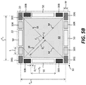
- FIG. 5B is a detail schematic of the exemplary micro-light-emitting-diode display illustrated in FIG. 5A and according to illustrative embodiments of the present invention
- FIG. 5C is a schematic plan view illustrating an exemplary micro-light-emitting-diode display in a high-resolution configuration comprising pixel micro-controllers that each control four pixels and pixels that each comprise three light-emitting elements disposed at the edges of the pixel micro-controllers, according to illustrative embodiments of the present invention
- FIG. 5D is a detail schematic of the exemplary micro-light-emitting-diode display illustrated in FIG. 5C and according to illustrative embodiments of the present invention.
- FIG. 6A is a schematic plan view illustrating a micro-light-emitting-diode display in a configuration comprising pixels that each comprise three light-emitting elements and pixel micro-controllers that each control one pixel, according to illustrative embodiments of the present invention
- FIG. 6B is a detail schematic of the micro-light-emitting-diode display illustrated in FIG. 6A and according to illustrative embodiments of the present invention
- FIG. 7 is an electrical schematic illustrating an exemplary pixel unit in a configuration comprising pixels that each comprise three light-emitting elements and pixel micro-controllers that each control two pixels, according to illustrative embodiments of the present invention
- FIG. 8 is a schematic plan view illustrating an exemplary arrangement of pixels in a configuration comprising pixels arranged in aligned rows and aligned columns, according to illustrative embodiments of the present invention
- FIG. 9 is a schematic plan view illustrating an exemplary arrangement of pixels in a configuration comprising pixels arranged in alternating offset rows and aligned columns, according to illustrative embodiments of the present invention.
- FIG. 10 is a schematic plan view corresponding to FIG. 9 with pixel units having a plus-shape indicated, according to illustrative embodiments of the present invention.
- FIG. 11A is a schematic plan view illustrating an exemplary arrangement of pixels in a configuration comprising pixels arranged in alternating offset rows and aligned columns wherein adjacent columns are disposed in a mirrored zigzag pattern arrangement, according to illustrative embodiments of the present invention
- FIG. 11B is a detail schematic of the exemplary micro-light-emitting-diode display illustrated in FIG. 11A and according to illustrative embodiments of the present invention
- FIG. 11C is a schematic plan view illustrating an exemplary arrangement of pixels using the pixel unit configuration of FIG. 11B , according to illustrative embodiments of the present invention.
- FIG. 12A is a schematic cross section illustrating an exemplary arrangement of pixels and a pixel micro-controller comprising micro-light-emitting elements and a pixel micro-controller disposed directly on a display substrate, according to illustrative embodiments of the present invention
- FIG. 12B is a schematic cross section illustrating an exemplary arrangement of pixels and a pixel micro-controller comprising micro-light-emitting elements and a pixel micro-controller adhered directly to a display substrate with an adhesive layer, according to illustrative embodiments of the present invention
- FIG. 12C is a schematic perspective illustrating an exemplary arrangement of pixels and a pixel micro-controller according to illustrative embodiments of the present invention in accordance with FIG. 12A ;
- FIG. 13A is a schematic cross section illustrating an exemplary arrangement of pixels and a pixel micro-controller comprising micro-light-emitting elements and the pixel micro-controller disposed directly on a pixel substrate, the pixel substrate disposed directly on a display substrate, according to illustrative embodiments of the present invention
- FIG. 13B is a schematic cross section illustrating an exemplary arrangement of pixels and a pixel micro-controller comprising micro-light-emitting elements and the pixel micro-controller adhered directly to a pixel substrate with an adhesive layer, the pixel substrate adhered directly to a display substrate with an adhesive layer, according to illustrative embodiments of the present invention
- FIG. 13C is a schematic perspective illustrating an exemplary arrangement of pixels and a pixel micro-controller according to illustrative embodiments of the present invention in accordance with FIG. 13A ;
- FIG. 14A is a schematic cross section illustrating an exemplary arrangement of pixels and a pixel micro-controller comprising micro-light-emitting elements disposed directly on a pixel micro-controller, the pixel micro-controller disposed directly on a display substrate, according to illustrative embodiments of the present invention
- FIG. 14B is a schematic cross section illustrating an exemplary arrangement of pixels and a pixel micro-controller comprising micro-light-emitting elements adhered directly to a pixel micro-controller with an adhesive layer, the pixel micro-controller adhered directly to a display substrate with an adhesive layer, according to illustrative embodiments of the present invention
- FIG. 14C is a schematic perspective illustrating an exemplary arrangement of pixels and a pixel micro-controller according to illustrative embodiments of the present invention in accordance with FIG. 14A ;
- FIGS. 14D, 14E, and 14F are schematic perspectives corresponding to either of the embodiments of FIGS. 14A and 14B illustrating exemplary arrangements of pixels according to illustrative embodiments of the present invention, where FIGS. 14D and 14E illustrate a rectangular pixel micro-controller and FIG. 14F has a plus-shaped or cross-shaped pixel micro-controller;
- FIG. 15A is a schematic plan view illustrating an exemplary active-matrix micro-light-emitting-diode display in a configuration comprising pixel micro-controllers that each control two pixels and pixels that each comprise three micro-light-emitting elements, together with row, column, and display controllers, according to illustrative embodiments of the present invention
- FIG. 15B is an electrical schematic illustrating an exemplary pixel unit corresponding to FIG. 15A , according to illustrative embodiments of the present invention.
- FIGS. 16A and 16B illustrate different pixel arrangements in one dimension on a pixel micro-controller, according to illustrative embodiments of the present invention
- FIGS. 17A-17D illustrate different pixel layouts in two dimensions on a pixel micro-controller, according to illustrative embodiments of the present invention.
- FIG. 18 is a schematic plan view illustrating an exemplary micro-light-emitting-diode display in a configuration comprising pixel units that each comprise two pixels and a pixel micro-controller with contact pads provided in a linear array on the pixel unit to facilitate electrical connections, according to illustrative embodiments of the present invention.
- Certain embodiments of the present invention provide an active-matrix micro-light-emitting-diode display with pixels and pixel micro-controllers disposed on or over a display substrate.
- Pixel micro-controllers control and drive two or more pixels that each comprise two or more micro-light-emitting elements, such as inorganic micro-light-emitting diodes.
- Shared control circuitry reduces a size of the pixel micro-controller, thereby reducing materials costs and a display fill factor.
- Pixels can comprise micro-light-emitting elements that are much smaller than a pixel micro-controller and can be located close together towards the ends of a pixel micro-controller.
- micro-light-emitting elements in a pixel can be much smaller than a pixel spacing and can be disposed close together, forming small pixels that are clearly separated, increasing resolution and improving pixel color integration for the human visual system during viewing, as well as providing space over a display substrate for redundant pixels (e.g., without sacrificing resolution).
- Pixels or components thereof, such as light-emitting elements
- Pixels can be mounted directly on or adhered directly to a display substrate, a pixel substrate, or a pixel micro-controller, further increasing resolution and providing space for redundant pixels and pixel controllers over a display substrate.
- an active-matrix micro-light-emitting-diode display 99 comprises a display substrate 10 , pixels 20 disposed in a pixel array on or over the display substrate 10 , and pixel micro-controllers 40 disposed in a controller array on the display substrate 10 .
- Pixels 20 in the pixel array can be arranged in rows of pixels 20 and columns of pixels 20 , as shown in FIG. 1A .
- Each pixel 20 comprises two or more micro-light-emitting elements 30 that emit different colors of light.
- Micro-light-emitting elements 30 can each have an element substrate that is independent, distinct, and separate from a display substrate 10 .
- Each pixel micro-controller 40 is electrically connected to control two or more micro-light-emitting elements 30 in each of two or more adjacent pixels 20 in a dimension in the pixel array, for example exclusively control (e.g., such that all micro-light-emitting elements 30 in a pixel are exclusively connected to one pixel micro-controller 40 ).
- Adjacent pixels 20 in a dimension are pixels 20 that have no intervening pixels 20 between the adjacent pixels 20 in the direction or dimension.
- a spatial separation between pixels 20 in each adjacent pair of pixels 20 in the pixel array controlled by a common pixel micro-controller 40 or between adjacent pairs of pixels 20 in the pixel array controlled by different pixel micro-controllers 40 is greater than a spatial separation between micro-light-emitting elements 30 in at least one pixel 20 in the pixel array
- the spatial separation between pixels 20 in each adjacent pair of pixels 20 in the pixel array controlled by a common pixel micro-controller 40 or between adjacent pairs of pixels 20 in the pixel array controlled by different pixel micro-controllers 40 is greater than a size of each of two or more micro-light-emitting elements 30 in at least one pixel 20 in the pixel array.
- a dimension can be a direction over an extent of the display substrate 10 , for example a surface of the display substrate 10 on or over which components (such as micro-light-emitting elements 30 or pixel micro-controllers 40 ) are disposed.
- a dimension is substantially parallel to one or more edges of a substrate (e.g., a display substrate 10 ).
- a dimension is not substantially parallel to any edge of a substrate (e.g., a display substrate 10 ).
- Two dimensions can be, but are not necessarily, orthogonal.
- all micro-light-emitting elements 30 in each pixel 20 are disposed in a common pixel direction P D orthogonal to a center line C L of a pixel micro-controller 40 and disposed an element distance D E substantially equal to or greater than one half of the extent or distance of the pixel micro-controller 40 in pixel direction P D from the center line C L .
- a pixel direction P D for each pixel 20 controlled by a common pixel micro-controller 40 from a center C of common pixel micro-controller 40 is different.
- each pixel 20 is disposed in a different pixel direction P D from a center C or center line C L of pixel micro-controller 40 that controls pixel 20 .
- Micro-light-emitting elements 30 in a common pixel 20 can be disposed in a common pixel direction P D from a center C or center line C L of pixel micro-controller 40 that controls the micro-light-emitting elements 30 in common pixel 20 .
- micro-light-emitting elements 30 in different pixels 20 controlled by a common pixel micro-controller 40 will be disposed in different pixel directions P D from a center C or center line C L of common pixel micro-controller 40 .
- a center line C L is a line through the center C of a pixel micro-controller 40 , for example, but not necessarily a line of symmetry for pixel micro-controller 40 .
- An element distance D E for each micro-light-emitting element 30 in a pixel 20 can be the same (as shown in FIG. 1B ) or different (not shown in FIG. 1B but illustrated, for example, in FIGS. 11B, 15B and discussed below).
- the at least one dimension is two dimensions, for example two orthogonal dimensions over an extent of the display substrate 10 , such as horizontal H and vertical V dimensions.
- each pixel micro-controller 40 controls at least two pixels 20 , for example two pixels 20 comprising a first pixel 20 and a second pixel 20 , each pixel 20 comprising two micro-light-emitting elements 30 .
- Micro-light-emitting elements 30 can have a width W and a length L over an extent of a display substrate 10 , for example a surface of display substrate 10 on or over which components such as micro-light-emitting elements 30 or pixel micro-controllers 40 are disposed.
- Micro-light-emitting elements 30 can be square with an aspect ratio of one so that W equals L or can have a non-unitary aspect ratio so that the width W and length L are different. Conventionally, and as used herein, the longer dimension is referred to arbitrarily as the length L.
- a first pixel 20 comprises only two micro-light-emitting elements 30 : a red micro-light-emitting element 30 R that emits red light and a green micro-light-emitting element 30 G that emits green light.
- a second pixel 20 comprises only two micro-light-emitting elements 30 : a blue micro-light-emitting element 30 B that emits blue light and a green micro-light-emitting element 30 G that emits green light.
- Red, green, or blue micro-light-emitting elements 30 R, 30 G, 30 B are collectively or generally referred to as micro-light-emitting elements 30 .
- Red, green, or blue micro-light-emitting elements 30 R, 30 G, 30 B in a pixel can be inorganic micro-light-emitting diodes ( ⁇ ILEDs), organic micro-light-emitting diodes ( ⁇ OLEDs), or any combination of ⁇ ILEDs and ⁇ OLEDs.
- adjacent pixels 20 in a pixel array are separated in a dimension by a distance D P and are disposed on a pixel pitch P.
- a dimension can be a horizontal dimension H or a vertical dimension V over display substrate 10 .
- a pixel pitch P is a distance defining the spatial frequency or repetition distance or spatial rate of pixels 20 in an array of pixels 20 in a direction or dimension.
- a pixel 20 can have a center or a centroid and a distance P between the centers or centroids of adjacent pixels 20 in a dimension can be a pixel pitch P in that dimension.
- the separation distance between pixels 20 is measured from an edge (e.g., a closest edge for adjacent pixels 20 ) of a pixel 20 .
- a pixel pitch P refers generically to a pixel pitch P H in the horizontal dimension H or a pixel pitch P V in the vertical dimension V.
- Adjacent pixels 20 in a pixel array can be separated by a distance (pixel spacing D P ) in both of two orthogonal dimensions (for example horizontal H and vertical V).
- a pixel spacing D P in both of the two orthogonal dimensions (e.g., H and V) can be the same, for example when horizontal and vertical pixel pitches P H and P V are the same and micro-light-emitting elements 30 are square.
- pixel spacing D P is not the same in both dimensions, but pixel pitch P is the same (P H equals P V ), for example if the micro-light-emitting elements 30 and pixels 20 are not square but the pixels 20 have equal pitches in two orthogonal dimensions (so that P H equals P V , for example, as shown in FIG. 1A ).
- a pixel unit 22 A comprises a single pixel micro-controller 40 together with the pixels 20 and micro-light-emitting elements 30 electrically connected to and controlled by the single pixel micro-controller 40 .
- a spatial separation D P between adjacent pixels 20 electrically connected to and controlled by a common pixel micro-controller 40 in a dimension is the same as a spatial separation D P between adjacent pixels 20 electrically connected to and controlled by different pixel micro-controllers 40 in the dimension, as indicated in FIG. 1A .
- Micro-light-emitting elements 30 in a pixel 20 are spatially separated by a distance D L , and can be spatially separated within a pixel 20 in a same direction as pixels 20 are separated in a pixel unit 22 or are spatially separated in a different direction, e.g., horizontal and vertical directions H, V, as also shown in FIG. 1A .
- a spatial separation D P between pixels 20 in each adjacent pair of pixels 20 in a common pixel unit 22 or between pixels 20 in adjacent different pixel units 22 in at least one dimension over an extent (e.g., surface) of a display substrate 10 is greater than a spatial separation D L between micro-light-emitting elements 30 in at least one pixel 20 in the pixel array, in either the same dimension or a different dimension.
- a spatial separation D P can be greater than a size (e.g., width W or length L) of each of two or more micro-light-emitting elements 30 in at least one pixel 20 in a pixel array.
- a spatial separation D P between adjacent pairs of pixels 20 is greater in a same dimension as the size of the two or more micro-light-emitting elements 30 .
- all micro-light-emitting elements 30 in each pixel 20 are disposed in a common pixel direction P D with respect to pixel micro-controller 40 that controls the pixel 20 .
- the direction P D is orthogonal to a center line C L of pixel micro-controller 40 .
- All micro-light-emitting elements 30 in each pixel 20 are disposed an element distance D E that is substantially equal to or greater than one half of an extent distance of a pixel micro-controller 40 in a pixel direction P D from a center line C L .
- Pixel direction P D for each pixel 20 controlled by a common pixel micro-controller 40 is different.
- some of the pixel directions P D are orthogonal to, or extend in an opposite direction from, other pixel directions P D .
- a pixel 20 A is disposed in a direction P DA an element distance D EA from center line C L and pixel 20 B is disposed in an opposite direction P DB an element distance D EB from center line C L .
- element distance D EA and element distance D EB are collectively referred to as element distances D E .
- Element distance D EA is equal to element distance D EB and both are greater than one quarter of a length of the pixel micro-controller 40 and greater than one half of the pixel micro-controller 40 from the center line C L .
- micro-light-emitting elements 30 of each pixel 20 By disposing micro-light-emitting elements 30 of each pixel 20 an element distance D E greater than one quarter of the length of pixel micro-controller 40 and greater than one half of the pixel micro-controller 40 from the center line C L , micro-light-emitting elements 30 in a pixel 20 are closer to an edge of pixel micro-controller 40 than to a center C or center line C L of the pixel micro-controller 40 .
- the pixel direction P D of each pixel 20 (pixel direction P DA for pixel 20 A and pixel direction P DB for pixel 20 B) is different. In the exemplary embodiment shown in FIG.
- micro-light-emitting elements 30 are disposed beyond an edge of pixel micro-controller 40 from a center C or center line C L of pixel micro-controller 40 , providing greater separation between pixels 20 in a common pixel unit 22 .
- a greater pixel separation D P and a smaller micro-light-emitting element separation D L provides improved color integration for a human viewer of the pixel 20 , so that the separate micro-light-emitting elements 30 in a common pixel 20 are less likely to be distinguished by the human visual system of a viewer (e.g., in certain embodiments, are not distinguishable).
- all micro-light-emitting elements 30 of a pixel 20 are disposed in a line, as shown in FIG. 1A .
- the line can be parallel to a pixel direction P D for the pixel 20 (as shown in FIG. 11B , discussed below), or the line can extend in a different direction, for example an orthogonal direction, as shown in FIG. 1B .
- micro-light-emitting elements 30 of a pixel 20 are disposed in a two-dimensional arrangement, for example at the corners of a triangle (e.g., as shown in FIG. 15A and discussed further below).
- a pixel micro-controller 40 can have a length greater than a width over a display substrate 10 and pixels 20 can be disposed at edges of a pixel micro-controller 40 in a length direction over an extent (e.g., surface) of the display substrate 10 , for example adjacent to or beyond the edges in the length direction, as shown in FIG. 1B .
- pixels 20 can be disposed within the width of the pixel micro-controller 40 so that the pixels 20 do not extend in the width direction a distance farther than one half the width of the pixel micro-controller 40 from a center C or a center line C L of the pixel micro-controller 40 (e.g., a horizontal center line C L , not shown in FIG. 1B ).
- pixel micro-controllers 40 are digital integrated circuit controllers that each include (e.g., incorporate) a digital circuit.
- Pixel units 22 can comprise contact pads 50 that provide an electrical contact and electrical connection to the digital circuits in the pixel micro-controllers 40 .
- Contact pads 50 can be disposed on or be a part of pixel micro-controllers 40 or disposed adjacent to pixel micro-controllers 40 as a part of pixel units 22 .
- a display substrate 10 can be any substrate capable of supporting pixels 20 and pixel micro-controllers 40 , for example glass, plastic, ceramic, sapphire, or quartz substrates.
- Display substrates 10 found in the display industry, for example as used in liquid crystal displays or organic light-emitting diode displays are suitable.
- Display substrates 10 can be rigid or flexible.
- a display substrate 10 has a substantially planar surface with a much smaller thickness.
- a display substrate 10 can have an area of 100 cm 2 to 10 m 2 and/or a thickness of 1 cm or less, 1 mm or less, 0.7 mm or less, 0.5 mm or less, or less.
- the extent of a display substrate 10 is taken over the larger substantially planar surface area on or over which the pixels 20 and pixel micro-controllers 40 are disposed.
- Micro-light-emitting elements 30 in pixels 20 can be any suitable electrically controllable light emitter.
- micro-light-emitting elements 30 are inorganic micro-light-emitting diodes ( ⁇ ILEDs), organic micro-light-emitting diodes ( ⁇ OLEDs), or any combination of ⁇ ILEDs and ⁇ OLEDs.
- micro-light-emitting elements 30 are ⁇ ILEDs formed in compound semiconductor materials such as GaN or GaAs or similar materials with doped additives such as, for example, aluminum or phosphide and having micron-sized dimensions, for example at least one of (i) a width from 2 to 100 ⁇ m (e.g., 2 to no more than 5 ⁇ m, 5 to no more than 10 ⁇ m, 10 to no more than 20 ⁇ m, 20 to no more than 50 ⁇ m, or 50 to no more than 100 ⁇ m), (ii) a length from 2 to 250 ⁇ m (e.g., 2 to no more than 5 ⁇ m, 5 to no more than 10 ⁇ m, 10 to no more than 20 ⁇ m, 20 to no more than 50 ⁇ m, 50 to no more than 100 ⁇ m, 100 to no more than 250 ⁇ m), and (iii) a thickness from 2 to 50 ⁇ m (e.g., 2 to no more than 5 ⁇ m, 5
- Light-emitting diodes with such dimensions can be assembled using micro-transfer printing and can have an element substrate that is independent, distinct, and separate from a display substrate 10 .
- Suitable ⁇ ILEDs can be vertical ⁇ ILEDs with electrode contacts on opposite sides of the ⁇ ILED or horizontal ⁇ ILEDs with electrode contacts on a same side of the ⁇ ILED.
- light-emitting elements 30 such as ⁇ ILEDs can be disposed on (e.g., directly on), adhered to, or over a display substrate 10 .
- light-emitting elements 30 such as ⁇ ILEDs are provided and disposed on or over display substrate 10 as unpackaged semiconductor integrated circuit devices, enabling smaller pixel unit 22 structures with better electronic and optical performance at higher resolution and with superior perceptual quality for active-matrix micro-light-emitting-diode displays 99 .
- Pixel micro-controllers 40 can be any circuit that controls two or more pixels 20 that each have two or more micro-light-emitting elements 30 .
- Pixel micro-controllers 40 can be integrated circuits, for example silicon complementary metal-oxide semiconductors (CMOS), can be mixed-signal circuits incorporating both digital and analog circuits, or can be analog circuits, and can also be micron-sized, for example having dimensions over the extent of a display substrate 10 (e.g., a length or width) of less than or equal to 100, 80, 60, 40, or 20 microns and/or a thickness of less than or equal to 40, 20, 15, 10, 8, or 5 microns.
- CMOS silicon complementary metal-oxide semiconductors
- Pixel micro-controllers 40 can be digital integrated circuit controllers, for example responsive to digital control signals and providing digital control to the micro-light-emitting elements 30 , for example using temporal pulse width modulation at a constant current.
- pixel micro-controllers 40 can be formed in, on (e.g., directly on), adhered to, or over a display substrate 10 , for example in a thin-film semiconductor layer disposed on the display substrate 10 .
- pixel micro-controllers 40 can be formed in a micro-controller substrate that is separate, distinct, and independent from a display substrate 10 , for example as an integrated circuit.
- Such integrated circuits can be formed in crystalline semiconductor materials that have a much greater electron mobility and much smaller transistors, providing electronic performance that is much superior to thin-film electronic devices and enabling much more complex and capable control of micro-light-emitting elements 30 in smaller devices.
- pixel micro-controllers 40 are provided and disposed on or over a display substrate 10 as unpackaged semiconductor integrated circuit devices, enabling smaller pixel unit 22 structures with better electronic and optical performance at higher resolution and with superior perceptual quality for active-matrix micro-light-emitting-diode displays 99 .
- micro-light emitting elements 30 are disposed at the ends of a pixel micro-controller 40 in the length direction so that pixel units 22 have a length much greater than a width so that more space is provided over a display substrate 10 between pixel units 22 in a vertical direction V than in a horizontal direction H.
- each pixel unit 22 is separated from an adjacent pixel unit 22 in a separation direction (e.g., vertical direction V) by a space greater than or equal to a size of pixel unit 22 in the separation direction so that space is provided for a redundant pixel unit location 24 between pixel unit 22 and an adjacent pixel unit 22 over the display substrate 10 in the separation direction (e.g., vertical direction V in FIG. 1A ).
- a redundant pixel unit 22 can be provided in the redundant pixel location 24 and electrically connected in parallel with the failed pixel unit 22 to provide light output from the redundant pixel unit 22 in place of the failed pixel unit 22 , thus improving manufacturing yields for micro-light-emitting-diode displays 99 .
- a redundant pixel unit 22 can be provided initially (e.g., prior to determining failure of a pixel unit 22 ) or after a failed pixel unit 22 has been determined.
- a redundant pixel unit 22 is a pixel unit 22 that is meant to behave substantially identically to another pixel unit 22 .
- pixel micro-controllers 40 having a different aspect ratio but substantially the same area as the exemplary embodiments illustrated in FIGS. 1A and 1B are disposed on or over a display substrate 10 .
- the aspect ratio of the different pixel micro-controller 40 shown in FIGS. 2A and 2B is more square than a substantially longer aspect ratio of pixel micro-controllers 40 in FIGS. 1A and 1B , enabling a higher density of pixel units 22 and a higher-resolution micro-light-emitting-diode display 99 .
- pixel units 22 are closer together than pixels 20 over a display substrate 10 in a same direction.
- FIGS. 1A and 1B are substantially the same as the illustrated areas of pixel micro-controllers 40 in FIGS. 2A and 2B .
- contact pads 50 in FIGS. 2A and 2B are also the same size as in FIGS. 1A and 1B , but those knowledgeable in the electronic layout arts will appreciate that the unused area in pixel units 22 of FIGS. 2A and 2B can be used to increase a size of contact pads 50 or pixel micro-controllers 40 or even to permit the use of larger micro-light-emitting elements 30 .
- each pixel micro-controller 40 in a micro-light-emitting-diode display 99 has a substantially rectangular shape with a center C and a length greater than a width over an extent (e.g., surface) of a display substrate 10 .
- the substantially rectangular shape comprises a first side opposing a second side in the length direction, where the length is greater than or equal to the width.
- Two or more pixels 20 electrically connected to a pixel micro-controller 40 can comprise a first pixel 20 and a second pixel 20 .
- First pixel 20 can be closer to the first side than to a point M mid-way between the center C and the first side, and second pixel 20 can be closer to the second side than to a point M mid-way between the center C and the second side. Locating the first and second pixels 20 closer to the mid-point M can increase the density and resolution of pixels 20 on or over a display substrate 10 .
- pixels 20 are relatively small and their micro-light-emitting elements 30 are spaced close together (D L ) compared to pixel micro-controller 40 , pixel pitch P, and pixel spacing D P .
- each pixel micro-controller 40 can have an area over a display substrate 10 that is larger than a combined area of each micro-light-emitting element 30 of the two or more pixels 20 electrically connected to and controlled by pixel micro-controller 40 .
- each pixel micro-controller 40 can have an area over a display substrate 10 that is larger than a combined area of the two or more pixels 20 electrically connected to and controlled by pixel micro-controller 40 , providing relatively smaller pixels 20 with improved visual response for viewers.
- FIGS. 1A, 1B, 2A, and 2B comprise two pixels 20 in each pixel unit 22 and two micro-light-emitting elements 30 in each pixel 20 .
- each of the two micro-light-emitting elements 30 in each pixel 20 emit different colors of light.
- each pixel micro-controller 40 is electrically connected to and controls at least a first pixel 20 A and a second pixel 20 B.
- First pixel 20 A can comprise a first green micro-light-emitting element 30 G that emits green light and a red micro-light-emitting element 30 R that emits red light and second pixel 20 B can comprise a second green micro-light-emitting element 30 G that emits green light and a blue micro-light-emitting element 30 B that emits blue light. Since the human visual system perceives high-frequency luminance primarily with green light and red and blue colors are not perceived with the same frequency response, two-color pixels 20 , each with a green emitter can provide a spatially efficient display system with a reduced number of micro-light emitting elements 30 and an increased number of pixels 20 and pixel units 22 in micro-light-emitting-diode displays 99 .
- each pixel 20 comprises three micro-light-emitting elements 30 , for example a red micro-light-emitting element 30 R that emits red light, a green micro-light-emitting element 30 G that emits green light, and a blue micro-light-emitting elements 30 B that emits blue light.
- each pixel 20 comprises four micro-light-emitting elements 30 , for example emitting red, green, blue, and white light respectively, or emitting red, green, blue, and yellow light respectively, or emitting red, green, blue, and cyan light respectively.
- pixels 20 can comprise any number of micro-light-emitting elements 30 .
- Micro-light-emitting elements 30 within a pixel 20 can each emit a different color of light than any others of the micro-light-emitting elements 30 within a pixel 20 .
- some micro-light-emitting elements 30 within a common pixel 20 can emit a same color of light as another of the micro-light-emitting elements 30 within the pixel 20 , for example to increase light output of a particular color or to provide redundancy.
- Those micro-light-emitting elements 30 in the common pixel 20 that emit a same color of light can have different attributes, such as different efficiencies, ranges, or luminance.
- a pixel 20 in a pixel unit 22 can have two green micro-light-emitting elements 30 G that are slightly different in a central frequency of emission, comprise different materials, have different external quantum efficiencies (EQEs), are driven at different currents, or have different structures, optical reflectors, or optical absorbers, or any combination of these.
- EQEs external quantum efficiencies
- the exemplary embodiment of FIG. 3A and the detail of FIG. 3B comprises pixels 20 with three micro-light-emitting elements 30 in each pixel 20 and a pixel micro-controller 40 with a substantially non-unitary aspect ratio, corresponding to the illustrative embodiments of FIGS. 1A and 1B , thereby providing redundant pixel unit locations 24 between adjacent pixel units 22 in the vertical dimension V.
- the illustrative embodiments of FIG. 4A and the detail of FIG. 4B are examples of micro-light-emitting-diode displays 99 with increased resolution, but without any redundant pixel unit locations 24 .
- FIGS. 1A, 1B, 2A, 2B and FIGS. 3A, 3B, 4A, 4B all comprise pixel units 22 having two pixels 20 electrically connected to and controlled by each pixel micro-controller 40 .
- a pixel micro-controller 40 can control three or four, or more, pixels 20 . Referring to the illustrative embodiments of FIGS.
- each pixel unit 22 comprises a pixel micro-controller 40 that controls four pixels 20 with three micro-light-emitting elements 30 each: a red micro-light-emitting element 30 R that emits red light, a green micro-light-emitting element 30 G that emits green light, and a blue micro-light-emitting element 30 B that emits blue light (totaling twelve micro-light-emitting elements 30 ).
- micro-light-emitting elements 30 are disposed at the corners of a pixel micro-controller 40 .
- micro-light-emitting elements 30 are disposed at the sides of a pixel micro-controller 40 .
- FIGS. 5A, 5B and FIGS. 5C, 5D comprise three micro-light-emitting elements 30 in each of four pixels 20
- a pixel 20 in accordance with any four of these exemplary embodiments could comprise only two micro-light-emitting elements 30 (e.g., as shown in FIGS. 1A and 1B ).
- pixel micro-controllers 40 have a rectangular and substantially square shape with each pixel 20 disposed adjacent to each of the four corners ( FIGS. 5A, 5B ) or sides ( FIGS. 5C, 5D ) of the pixel micro-controllers 40 . In some embodiments (e.g., as shown in FIG.
- pixel micro-controllers 40 are plus-shaped (having a shape similar to a plus ‘+’ sign or character), cross-shaped, or x-shaped (having a shape similar to an ‘x’ letter or character that is a rotated version of a plus sign shape) with each pixel 20 disposed adjacent to each of the four extended portions of the pixel micro-controllers 40 farthest from a center C or center-line C L of the pixel micro-controllers 40 .
- the substantially rectangular shape or plus shape of FIGS. 5A and 5B comprises a first side opposing a second side in a first dimension (e.g., horizontal dimension H) and the two or more pixels 20 electrically connected to a pixel micro-controller 40 comprise a first pixel 20 and a second pixel 20 .
- First pixel 20 can be closer to the first side than to a point M mid-way between a center C (or center line C L ) and the first side.
- second pixel 20 can be closer to the second side than to a point M mid-way between a center C (or center line C L ) and the second side.
- a substantially rectangular shape or plus shape can further comprise a third side opposing a fourth side in a second dimension orthogonal to the first dimension (e.g., a vertical dimension V) and two or more pixels 20 further comprise a third pixel 20 and a fourth pixel 20 .
- the third pixel 20 can be closer to the third side than to a center C (or center line C L ), and the fourth pixel 20 can be closer to the fourth side than to the center C (or center line C L ).
- first, second, third, and fourth pixels 20 have an aspect ratio greater than one but, since first and second pixels 20 are rotated with respect to third and fourth pixels so that the distance between first and second pixels 20 is substantially the same as a distance between third and fourth pixels 20 , horizontal pixel pitch P H is substantially equal to vertical pixel pitch P V .
- a spatial separation between pixels 20 for each adjacent pair of pixels 20 in a pixel array is greater than a spatial separation between micro-light-emitting elements 30 in at least one pixel 20 in the pixel array in at least one dimension over the extent of a display substrate 10 .
- the spatial separation between pixels 20 in a pixel unit 22 or between pixels 20 in adjacent pixel units 22 is greater than a size of each of the two or more micro-light-emitting elements 30 in at least one pixel 20 in the pixel array.
- All of the two or more micro-light-emitting elements 30 in each pixel 20 are disposed in a common pixel direction P D orthogonal to a center line C L of pixel micro-controller 40 an element distance D E substantially equal to or greater than one quarter of the extent of pixel micro-controller 40 in pixel direction P D from a center line C L .
- Pixel direction P D for each pixel 20 controlled by a common pixel micro-controller 40 is different. As shown in FIGS.
- the pixel 20 on the left side of a pixel unit 22 has a pixel direction P D from a vertical center line C L that is horizontal to the left
- the pixel 20 on the right side of the pixel unit 22 has a pixel direction P D from a vertical center line C L that is horizontal to the right
- the pixel 20 on the top side of the pixel unit 22 has a pixel direction P D from a horizontal center line C L that is vertical and up (towards the top)
- the pixel 20 on the bottom side of the pixel unit 22 has a pixel direction P D from a horizontal center line C L that is vertical and down (towards the bottom).
- the element distances D E for pixels 20 are substantially the same magnitude, but each has a different direction P D .
- a micro-light-emitting-diode display comprises pixels 20 in which independent micro-controllers 41 each control a single pixel 20 comprising a red micro-light-emitting element 30 R, a green, micro-light-emitting element 30 G, and a blue micro-light-emitting element 30 B. Because the independent micro-controllers 41 control only three micro-light-emitting elements 30 in a single pixel 20 , they each require less circuitry and area than pixel micro-controllers 40 of FIGS.
- pixel micro-controllers 40 that each drive multiple pixels 20 each comprising multiple micro-light-emitting elements 30 have a reduced area compared to the combined area of multiple pixel micro-controllers 40 that each control a single pixel 20 or micro-light-emitting element 30 .
- micro-light-emitting-diode displays 99 with greater pixel density and increased resolution together with smaller control circuits, reduced costs, and improved visual color integration are provided.
- a digital pixel micro-controller 40 has been designed, constructed, and put into use that increases in size by approximately 12% for each additional micro-light-emitting element 30 to be controlled by the digital pixel micro-controller 40 .
- pixel micro-controllers 40 in accordance with the exemplary embodiments illustrated in FIGS. 1A, 1B, 2A, 2B ) that control two pixels 20 each having two micro-light-emitting elements 30 require approximately 40% less area than two micro-controllers 41 illustrated in FIGS. 6A and 6B that each control only a single pixel 20 .
- Pixel micro-controllers 40 in accordance with the exemplary embodiments illustrated in FIGS. 3A, 3B, 4A, 4B that control two pixels 20 each having three micro-light-emitting elements 30 require approximately 33% less area than two micro-controllers 41 .
- FIGS. 1A, 1B and FIGS. 2A, 2B include four micro-light-emitting elements 30 , for clarity the illustrated area of pixel micro-controller 40 is increased by approximately 12% compared to micro-controllers 41 of FIGS. 6A and 6B that control three micro-light-emitting elements 30 .
- 4A, 4B include two pixels 20 with six micro-light-emitting elements 30 and, for clarity the illustrated area of pixel micro-controller 40 is increased by approximately 50% compared to micro-controllers 41 of FIGS. 6A, 6B .
- pixel micro-controller 40 of FIGS. 5A and 5B are approximately increased by approximately 200% so as to illustrate the size increase for pixel micro-controllers 40 that control four pixels 20 and twelve micro-light-emitting elements 30 .
- a pixel micro-controller 40 can be provided in a digital integrated circuit with mixed-signal drive circuitry (driver 46 ) and digital control circuitry (control circuit 42 , memory 44 ).
- a single control circuit 42 can be used to control all of the micro-light-emitting elements 30 electrically connected to the pixel micro-controller 40 (e.g., a red micro-light-emitting element 30 R, a green micro-light-emitting element 30 G, and a blue micro-light-emitting element 30 B for each of two pixels 20 ).
- a memory 44 can store signals specifying the light output of each micro-light-emitting element 30 .
- the pixel micro-controller 40 comprises pixel portions that each exclusively controls a pixel 20 electrically connected to the pixel micro-controller 40 (e.g., drivers 46 , and portions of the memory 44 ), and a shared portion that provides control in common to all pixels 20 electrically connected to the pixel micro-controller 40 (e.g., control circuit 42 and contact pads 50 ).
- an external display controller 18 (e.g., as shown in FIG. 15A and including row controller 16 and column controller 14 , discussed below) provides power 56 , ground 58 , column data signals 52 , and row control signals 54 through wires 62 formed on a display substrate 10 to contact pads 50 .
- Contact pads 50 are electrically connected to a pixel micro-controller 40 .
- the pixel micro-controller 40 receives the signals and stores the column data information in a memory 44 using a control circuit 42 . Once the column data information is stored, control circuit 42 provide signals to drivers 46 that drive the respective two or more micro-light-emitting elements 30 of each pixel 20 .
- Each micro-light-emitting element 30 receives a current signal at a desired voltage from a respective driver 46 and is connected to a ground 58 line so that a voltage differential is provided across micro-light-emitting elements 30 and micro-light-emitting elements 30 emit light.
- pixels 20 are distributed in a strictly regular array with aligned rows and aligned columns of pixels 20 so that all of the rows are spaced a common distance from an edge of a display substrate 10 and all of the columns are spaced a common distance from another edge of the display substrate 10 , for example an edge that is orthogonal to the edge from which the rows are commonly spaced.
- Such an arrangement is readily constructed in accordance with the embodiments illustrated in FIGS. 1A, 1B, 2A, 2B, 3A, 3B, 4A, 4B, and 5A, 5B .
- pixels 20 in an array are disposed in rows and columns and alternating rows are offset in a row direction or alternating columns are offset in a column direction (not shown), or both, for example constructed in accordance with embodiments illustrated in FIGS. 1A, 1B, 2A, 2B, 3A, 3B , and 4 A, 4 B (e.g., having similar pixel units).
- FIG. 10 illustrates an exemplary embodiment comprising offset alternating rows using plus-shaped pixel micro-controllers 40 (e.g., as illustrated in FIG. 14F ).
- the embodiments of FIGS. 5C and 5D can have alternating sets of three rows that are offset from adjacent sets of three rows. The center row of each set of three has twice the number of pixels 20 . This arrangement, with suitable pixel processing, can provide increased display resolution.
- pixel micro-controller 40 and micro-light-emitting elements 30 or pixels 20 in a pixel unit 22 are disposed in a line, for example a line that passes through each of pixel micro-controller 40 and micro-light-emitting elements 30 or a line that passes through the center C or centroid of pixel micro-controller 40 and micro-light-emitting elements 30 or pixels 20 .
- contact pads 50 , centers of contact pads 50 , or centroids of contact pads 50 are in a same line.
- Pixels 20 can each comprise two or three micro-light-emitting elements 30 , or more.
- contact pads 50 are disposed between a pixel micro-controller 40 and micro-light-emitting elements 30 or between a pixel micro-controller 40 and only some micro-light-emitting elements 30 .
- micro-light-emitting elements 30 are between contact pads 50 and a pixel micro-controller 40 , so that contact pads 50 are at the ends of the pixel micro-controller 40 .
- pixels 20 in a dimension are spaced further apart, so that pixels 20 in a common pixel unit 22 are closer together than pixels 20 in different pixel units 22 .
- pixels 20 in the pixel array are disposed in rows and columns, each column of pixels 20 forms a zigzag pattern 26 , adjacent columns are mirror reflections of each other, and a distance D 2 between pixels 20 in a pixel unit 22 is less than a distance D 1 between pixels 20 in adjacent pixel units 22 in a same dimension.
- Adjacent pixel columns that are mirror reflections have pixels 20 that are alternately closer together and farther apart in each row in the columns. (The micro-light-emitting elements 30 in pixels 20 are not necessarily disposed in a mirrored arrangement but can have the same arrangement in every pixel 20 , regardless of row or offset.)
- Disposing pixel units 22 over a display substrate 10 with a common orientation and contact pads 50 disposed in a line with pixel micro-controller 40 and micro-light-emitting elements 30 enables a straightforward arrangement of wires 62 that provide power 56 , ground 58 , and control signals (e.g., row control signals 54 and column data signals 52 ) on or over the display substrate 10 (e.g., as shown in FIG. 18 ).
- wires 62 carry power 56 , ground 58 , column data signals 52 , and row control signals 54 to contact pads 50 and thence to a pixel micro-controller 40 that controls the pixels 20 .
- Wires 62 can be arranged in a vertical parallel arrangement that reduces cross-overs on a display substrate 10 .
- pixel units 22 can be arranged in different orientations over a display substrate 10 .
- Certain embodiments of the present invention can be constructed using micro-transfer printing.
- devices or components such as micro-inorganic light-emitting diodes or pixel micro-controllers 40 are formed on a native source substrate using photolithographic methods.
- the devices are then released from the native source substrate by removing a sacrificial portion from beneath each device or component, leaving the devices or components attached to anchor portions of the native source substrate with tethers.
- a stamp then contacts the devices, breaking or separating the tethers and adhering the devices to the stamp.
- the stamp is moved to a destination substrate and the devices with a broken or separated tether are contacted to the destination substrate, a layer on the destination substrate, or an adhesive layer disposed on the destination substrate.
- the devices with a broken or separated tether are adhered to the destination substrate, destination substrate layer, or destination substrate adhesive layer, and the stamp removed.
- Micro-transfer printing methods can be employed to make a variety of structures in a corresponding variety of embodiments.
- each pixel micro-controller 40 and the two or more micro-light-emitting elements 30 of each of pixels 20 controlled by the pixel micro-controller 40 are disposed directly on or adhered directly to a display substrate 10 or a layer formed on the display substrate 10 , for example an adhesive layer.
- an adhesive layer 12 is disposed on a display substrate 10 or layer formed on the display substrate 10 to facilitate adhesion between the display substrate 10 and pixel micro-controllers 40 and between the display substrate 10 and the two or more micro-light-emitting elements 30 of each pixel 20 .
- Adhesive layer 12 can be a curable layer that is cured after the pixel micro-controllers 40 and the two or more micro-light-emitting elements 30 of each pixel 20 are disposed on (e.g., micro-transfer printed to) adhesive layer 12 .
- the display substrate 10 , pixel micro-controllers 40 , and the two or more micro-light-emitting elements 30 of each pixel 20 can then be photolithographically processed to provide wires 62 (e.g., as shown in FIG. 12C ) to electrically connect pixel units 22 to a row controller 16 and column controller 14 , for example through contact pads 50 .
- pixel micro-controllers 40 and micro-light-emitting elements 30 can each have a broken or separated tether (e.g., as shown in FIGS. 13A and 13B ).
- pixel micro-controllers 40 and inorganic micro-light-emitting elements 30 can be independent structures that are individually mounted on a display substrate 10 , for example by micro-transfer printing the independent structures onto the display substrate 10 .
- a micro-light-emitting-diode display 99 comprises pixel substrates 60 arranged in an array on a display substrate 10 .
- a pixel substrate 60 can be any substrate capable of supporting pixels 20 and pixel micro-controllers 40 , for example glass, plastic, ceramic, sapphire, quartz, or a semiconductor, such as a silicon wafer, and is separate, distinct, and independent of a display substrate 10 or any micro-light-emitting element 30 substrate.
- a pixel substrate 60 can comprise or be the same material as is used in a display substrate 10 and, independently, can be rigid or flexible.
- a pixel substrate 60 has a substantially planar surface with a much smaller thickness.
- a pixel substrate 60 can have an area of 10 cm 2 or less and thicknesses in the range of 1 mm to 0.01 mm, or less.
- the two or more micro-light-emitting elements 30 and pixel micro-controller 40 electrically connected to control pixel 20 are disposed directly on or adhered directly to a pixel substrate 60 or a layer formed on pixel substrate 60 , for example by micro-transfer printing from one or more source substrates or wafers to the pixel substrates 60 .
- an adhesive layer 12 adheres the two or more micro-light-emitting elements 30 of each pixel 20 and a pixel micro-controller 40 to a pixel substrate 60 .
- Pixel substrates 60 can themselves be prepared on a source wafer or substrate, for example silicon or glass, with micro-light-emitting elements 30 electrically connected by wires 62 to pixel micro-controller 40 in a pixel unit 22 and then micro-transfer printed to a display substrate 10 .
- pixel substrates 60 can comprise a broken or separated tether 64 as well as pixel micro-controller 40 and micro-light-emitting elements 30 (e.g., as shown in FIGS. 13A and 13B ).
- pixel micro-controllers 40 and the two or more micro-light-emitting elements 30 of each pixel 20 can be disposed directly on or adhered directly to a pixel substrate 60 or adhered to an adhesive layer 12 disposed on the pixel substrate 60 .
- pixel substrate 60 can be disposed directly on or adhered directly to a display substrate 10 or adhered to an adhesive layer 12 disposed on a display substrate 10 .
- pixel micro-controllers 40 and inorganic micro-light-emitting elements 30 can be independent structures that are individually mounted on a pixel substrate 60 , for example by micro-transfer printing the independent structures onto the pixel substrate 60 .
- a micro-light-emitting-diode display 99 comprises two or more micro-light-emitting elements 30 of each pixel 20 disposed directly on ( FIG. 14A ) or adhered directly to pixel micro-controller 40 ( FIG. 14B ) or are disposed directly on or adhered directly to a layer formed on pixel micro-controller 40 .
- an adhesive layer 12 adheres two or more micro-light-emitting elements 30 of each pixel 20 to a pixel micro-controller 40 . As illustrated in FIGS.
- pixels 20 and micro-light-emitting elements 30 can be disposed in various locations on or over a pixel micro-controller 40 .
- FIG. 14D shows pixels 20 disposed near edges of a rectangular pixel micro-controller 40
- FIG. 14E shows pixels 20 near corners of a rectangular pixel micro-controller 40
- FIG. 14F shows pixels 20 near edges of a plus-shaped pixel micro-controller 40 .
- plus-shaped pixel micro-controllers 40 can closely tile a display substrate 10 , increasing display resolution and reducing native source wafer costs by reducing waste.
- pixels 20 comprising micro-light-emitting elements 30 electrically connected to and controlled by pixel micro-controllers 40 comprising pixel units 22 can be disposed in a variety of configurations over display substrate 10 .
- any combination of pixel micro-controllers 40 , pixel units 22 , pixels 20 , and micro-light-emitting elements 30 can have a non-unitary aspect ratio and a length greater than a width over a display substrate 10 .
- any pixel micro-controllers 40 , pixel units 22 , pixels 20 , and micro-light-emitting elements 30 with respect to any other pixel micro-controllers 40 , pixel units 22 , pixels 20 , and micro-light-emitting elements 30 can be different.
- some of pixels 20 can be rotated with respect to others of pixels 20 over or on a display substrate 10 , either within a pixel unit 22 (for example as shown in FIGS. 5A-5D, 14D, and 14E ) or between pixel units 22 (for example as additionally shown in FIG. 11C ).
- At least some of the micro-light-emitting elements 30 in a pixel 20 are rotated with respect to other micro-light-emitting elements 30 in the same pixel 20 (for example as shown in FIGS. 5A-5D ) over a display substrate 10 .
- at least some micro-light-emitting elements 30 in pixels 20 are rotated with respect to a pixel micro-controller 40 (for example as shown in FIGS. 2A-2B, 4A-4B, and 11B ) over the display substrate 10 . Two or more devices or components are rotated when the longest dimensions of the devices or components are not aligned in the same direction.
- micro-light-emitting elements 30 within a pixel 20 are disposed in a line over a display substrate 10 (for example as shown in FIGS. 1A-4D and FIGS. 11A-14F ). In some other embodiments, micro-light-emitting elements 30 within a pixel 20 are not disposed in a line over a display substrate 10 . Referring to FIG. 15A and the detail of FIG. 15B , micro-light-emitting elements 30 within a pixel 20 are disposed at the corners of a triangle over a display substrate 10 (also as shown in FIGS. 5A-5B ). Contact pads 50 are disposed adjacent to the sides of a pixel micro-controller 40 (as in FIG.
- Each contact pad 50 is electrically connected to one of power 56 , ground 58 , row control signals 54 , and column data signals 52 distributed on wires 62 on a display substrate 10 from a display controller 18 , column controller 14 , and row controller 16 .
- column controller 14 and row controller 16 can be considered as a part of a larger display controller 18 .
- Contact pads 50 are electrically connected to pixel micro-controller 40 with wires 62 and micro-light-emitting elements 30 (e.g., red micro-light-emitting element 30 R, green micro-light-emitting element 30 G, and blue micro-light-emitting element 30 B for each pixel 20 in a pixel unit 22 ).
- micro-light-emitting elements 30 e.g., red micro-light-emitting element 30 R, green micro-light-emitting element 30 G, and blue micro-light-emitting element 30 B for each pixel 20 in a pixel unit 22 .
- each pixel 20 in a pixel unit 22 is disposed closer to an edge of a pixel micro-controller 40 that controls the pixel 20 than a mid-point M between the edge and a center C of the pixel micro-controller 40 or even on a side of the edge opposite the mid-point M or center C.
- pixel separation and color integration are increased, for example, as shown in FIG. 16A (for two pixels 20 in a pixel unit 22 ) and FIGS.
- each pixel 20 in a pixel unit 22 is disposed closer to a mid-point M between the edge and a center C of the pixel micro-controller 40 , as shown in FIG. 16B (for two pixels 20 in a pixel unit 22 ) and FIGS. 17B, 17D (for four pixels 20 in a pixel unit 22 ) for any of the configurations shown in FIGS. 12A-14E .
- This arrangement has the effect of reducing the pixel spacing and pixel pitch P and increasing the resolution.
- the arrangement of FIG. 16B is particularly useful for pixel 20 configurations such as those shown in FIG. 11A and, in two dimensions, the arrangements of FIGS. 17B and 17D .
- each micro-light-emitting element 30 of two or more micro-light-emitting elements 30 in at least one pixel 20 is an inorganic micro-light-emitting diode, for example all micro-light-emitting elements 30 in a micro-light-emitting diode display 99 are inorganic micro-light-emitting diodes.
- each micro-light-emitting element 30 of two or more micro-light-emitting elements 30 in at least one pixel 20 is an organic light-emitting diode, for example all micro-light-emitting elements 30 in a micro-light-emitting diode display 99 are organic micro-light-emitting diodes.
- At least one of the micro-light-emitting elements 30 of two or more micro-light-emitting elements 30 in at least one pixel 20 is an inorganic micro-light-emitting diode and at least one micro-light-emitting element 30 of two or more micro-light-emitting elements 30 in a pixel 20 or another pixel 20 commonly controlled by a pixel micro-controller 40 is an organic micro-light-emitting diode.
- a micro-light-emitting-diode display 99 in accordance with certain embodiments of the present invention can include both organic and inorganic micro-light-emitting diodes in any combination.
- pixels 20 can each comprise three micro-light-emitting elements 30 , a micro-light-emitting element 30 that is a red organic micro-light-emitting diode that emits red light, a micro-light-emitting element 30 that is a green organic micro-light-emitting diode that emits green light, and a micro-light-emitting element 30 that is a blue inorganic micro-light-emitting diode that emits blue light.
- each pixel micro-controller 40 controls two or more pixels 20 comprising a first pixel 20 and a second pixel 20 .
- a first pixel 20 comprises a red organic micro-light-emitting diode that emits red light and a green organic micro-light-emitting diode that emits green light and a second pixel 20 comprises a blue inorganic micro-light-emitting diode that emits blue light and a green organic micro-light-emitting diode that emits green light.
- the first pixel 20 comprises only two micro-light-emitting elements 30 : the red organic micro-light-emitting diode and the green organic micro-light-emitting diode.
- the second pixel 20 comprises only two micro-light-emitting elements 30 : the green organic micro-light-emitting diode and the blue inorganic micro-light-emitting diode.
- the first pixel 20 comprises only two micro-light-emitting elements 30 , the red organic micro-light-emitting diode and the green organic micro-light-emitting diode
- the second pixel 20 comprises only two micro-light-emitting elements 30 , the green organic micro-light-emitting diode and the blue inorganic micro-light-emitting diode.
- micro-light-emitting elements 30 can emit light in a direction away from a display substrate 10 (a top emitter) and the display substrate 10 can be substantially opaque (for example less than 50%, 30%, 20%, or 10% transparent to visible light) or substantially transparent (for example greater than 50%, 70%, 80%, or 90% transparent to visible light).
- micro-light-emitting elements 30 can emit light in a direction toward a display substrate 10 (a bottom emitter) and the display substrate 10 can be substantially transparent (for example greater than 50%, 70%, 80%, 90%, or 95% transparent to visible light).
- any pixel substrate 60 can be substantially opaque (for example less than 50%, 30%, 20%, or 10% transparent to visible light) or substantially transparent (for example greater than 50%, 70%, 80%, 90%, or 95% transparent to visible light). If visible light is emitted through a pixel substrate 60 from micro-light-emitting elements 30 , pixel substrates 60 are preferably substantially transparent (for example greater than 50%, 70%, 80%, 90%, or 95% transparent to visible light).
- a display substrate 10 and pixel substrates 60 can be either flexible or rigid.
- a micro-light-emitting-diode display 99 is a substantially single-layer display in which wires 62 (e.g., row control signals 54 , column data signals 52 , power 56 , and ground 58 wires 62 ) are disposed substantially in a single layer in, on, or over a display substrate 10 and pixel units 22 are also disposed in, on, or over display substrate 10 , for example in or on the same single layer.
- wires 62 e.g., row control signals 54 , column data signals 52 , power 56 , and ground 58 wires 62
- pixel units 22 are also disposed in, on, or over display substrate 10 , for example in or on the same single layer.
- wires 62 intersect on, in, or over display substrate 10
- a jumper wire or via connection can be provided but these jumper wires or connections represent only a small fraction of the area of display substrate 10 , so that wires 62 are substantially disposed in a single layer, for example a single patterned layer of metal lines that provide electrical connections to pixel units 22 .
- manufacturing costs and materials for a micro-light-emitting-diode display 99 can be substantially reduced (e.g., due to a reduced number of photolithographic processing steps).
- Certain embodiments of the present invention provide improved image display architectures for displays (for example light-emitting diode displays) having improved resolution, fewer or smaller micro-integrated circuits with reduced material costs, higher yields with reduced manufacturing costs, and improved visual quality.
- a column controller 14 is electrically connected to each column data signal 52 wire 62 and is disposed on a display substrate 10 .
- a column controller 14 for all of the column data signal 52 wires 62 can be a single integrated circuit, for example having a single column-controller substrate separate, distinct, and independent from a display substrate 10 , from pixel micro-controller 40 substrates, from pixel substrates 60 , and from micro-light-emitting element 30 substrates in pixels 20 .
- a column controller 14 comprises a plurality of column-controller integrated circuits, each electrically connected to one or more column data signal 52 wires 62 , and each having a column-controller substrate separate, distinct, and independent from a display substrate 10 , from micro-light-emitting element 30 substrates in pixels 20 , and from any other column-driver integrated circuit.
- a row controller 16 is electrically connected to each row control signal 54 wire 62 and is disposed on a display substrate 10 .
- a row controller 16 for all of the row control signal 54 wires 62 can be a single integrated circuit, for example having a single row-controller substrate separate, distinct, and independent from a display substrate 10 , from pixel micro-controller 40 substrates, from pixel substrates 60 , and from micro-light-emitting element 30 substrates in pixels 20 .
- a row controller 16 comprises a plurality of row-controller integrated circuits, each electrically connected to one or more row control signal 54 wires 62 , and each having a row-controller substrate separate, distinct, and independent from a display substrate 10 , from pixel substrates 60 , from micro-light-emitting element 30 substrates in pixels 20 , and from any other column-driver integrated circuit.
- pixel micro-controllers 40 in pixel units 22 are electrically connected to and control two or more micro-light-emitting elements 30 in two or more pixels 20 .
- the information for driving micro-light-emitting elements 30 of two or more pixels 20 can be transmitted through a single contact pad 50 connected to a single column data signal 52 wire 62 .
- row control signals 54 can be transmitted through a single contact pad 50 connected to a single row control signal 54 wire 62 .
- a single column data signal 52 wire 62 can provide information for multiple pixels 20 or for multiple micro-light-emitting elements 30 in one or more columns of pixels 20 and a single row control signal 54 wire 62 can provide control for multiple pixels 20 or for multiple micro-light-emitting elements 30 in one or more rows of pixels 20 .
- a micro-light-emitting-diode display 99 can have fewer column data signal 52 wires 62 than columns of pixels 20 or columns of micro-light-emitting elements 30 .
- a micro-light-emitting-diode display 99 can have fewer row control signal 54 wires 62 than rows of pixels 20 or rows of micro-light-emitting elements 30 .
- a pixel micro-controller 40 is a micro-integrated circuit, for example comprising a controller substrate separate, distinct, and independent of any micro-light-emitting element 30 substrates and display substrate 10 , made using photolithographic methods and materials found in the integrated circuit industry.
- Column data signal 52 wires 62 and row control signal 54 wires 62 (and power 56 and ground 58 wires 62 ) are electrically conductive wires, e.g., traces, for conducting electrical power and signals to pixel units 22 and can be made, for example, using photolithographic, screen printing, or printed-circuit board materials and methods on or in the display substrate 10 .
- Inorganic micro-light-emitting diodes can comprise a semiconductor diode substrate, for example a compound semiconductor such as GaN, InGaN, GaAs, or other compound semiconductors useful for inorganic micro-light-emitting diodes made using photolithographic processes and materials.
- a semiconductor diode substrate for example a compound semiconductor such as GaN, InGaN, GaAs, or other compound semiconductors useful for inorganic micro-light-emitting diodes made using photolithographic processes and materials.
- each inorganic micro-light-emitting diode has at least one (e.g., any combination) of (i) a width from 2 to 100 ⁇ m (e.g., 2 to no more than 5 ⁇ m, 5 to no more than 10 ⁇ m, 10 to no more than 20 ⁇ m, 20 to no more than 50 ⁇ m, or 50 to no more than 100 ⁇ m), (ii) a length from 2 to 250 ⁇ m (e.g., 2 to no more than 5 ⁇ m, 5 to no more than 10 ⁇ m, 10 to no more than 20 ⁇ m, 20 to no more than 50 ⁇ m, 50 to no more than 100 ⁇ m, or 100 to no more than 250 ⁇ m), and (iii) a thickness from 2 to 50 ⁇ m (e.g., 2 to no more than 5 ⁇ m, 5 to no more than 10 ⁇ m, 10 to no more than 20 ⁇ m, or 20 to no more than 50 ⁇ m).
- a width from 2 to 100 ⁇ m
- micro-light-emitting elements 30 inorganic or organic micro-light-emitting diodes, row controllers 16 , column controllers 14 , pixel micro-controllers 40 , or pixel substrates 60 can be micro-devices micro-transfer printed from a native source wafer to a display substrate 10 , another substrate, or to a substrate disposed on the display substrate 10 such as a pixel substrate 60 .
- Any organic or inorganic micro-light-emitting diodes, micro-light-emitting elements 30 , row controllers 16 , column controllers 14 , pixel micro-controllers 40 , or pixel substrates 60 can comprise a broken (e.g., fractured) or separated tether 64 as a consequence of the micro-transfer printing process.
- a pixel substrate 60 is micro-transfer printed from a pixel source wafer onto a display substrate 10 and a pixel substrate 60 comprises a broken (e.g., fractured) or separated pixel tether 64 .
- a pixel substrate 60 can have at least one of (i) an area of 10 to no more than 1 square mm (e.g., 10 to no more than 50 square microns, 50 to no more than 100 square microns, 100 to no more than 500 square microns, or 500 square microns to no more than 1 square mm) and (ii) a thickness of 1 to no more than 50 microns (e.g., 1 to no more than 5 microns, 5 to no more than 10 microns, 10 to no more than 20 microns, or 20 to no more than 50 microns).
- Such small pixel substrates 60 can be more readily micro-transfer printed and constructed using high-resolution photolithographic techniques.
- pixel-substrate wires 62 or other electrical conductors disposed on the pixel substrates 60 can be formed using, for example, photolithographic methods and materials and have a small width, can be disposed closer together, and can have a higher resolution than wires 62 or other electrical conductors such as row control signal 54 wires 62 and column data signal 52 wires 62 formed on a display substrate 10 , for example by large-format photolithography, screen printing, or printed-circuit board construction and assembly techniques.
- pixel-substrate wires 62 on a pixel substrate 60 can be relatively fine, high-resolution wires 62 and wires 62 on a display substrate 10 (e.g., row control signal 54 wires 62 , column data signal 52 wires 62 , power 56 wires 62 , and ground 58 wires 62 ) can be relatively coarse, low-resolution wires 62 compared to the relatively fine, high-resolution wires 62 on the pixel substrate 60 .
- Pixel substrate 60 wires 62 can be fine interconnections, for example having a width of less than 50 ⁇ m, less than 20 ⁇ m, less than 10 ⁇ m, less than five ⁇ m, less than two ⁇ m, or less than one ⁇ m.
- Row control signal 54 wires 62 , column data signal 52 wires 62 , power 56 wires 62 , and ground 58 wires 62 can include one or more crude lithography interconnections having a width from 2 ⁇ m to 2 mm. Therefore, in some embodiments of the present invention, high-resolution pixel substrates 60 are individually mounted on a display substrate 10 and micro-light-emitting elements 30 and pixel micro-controllers 40 are micro-devices individually mounted on each high-resolution pixel substrate 60 .
- Row control signal 54 wires 62 , column data signal 52 wires 62 , power 56 wires 62 , and ground 58 wires 62 can each, separately, comprise metal or metal alloys or transparent metal oxides (for example deposited on the display substrate 10 or pixel substrate 60 by evaporation or sputtering and patterned using photolithographic methods).
- Row control signal 54 wires 62 , column data signal 52 wires 62 , power 56 wires 62 , and ground 58 wires 62 can each, separately, be disposed on or in a single layer or on or in multiple (e.g., different) substrate layers of a display substrate 10 or pixel substrate 60 so that they do not electrically short on a surface of a display substrate 10 or pixel substrate 60 .
- Vias can be provided to make electrical connections between devices or structures disposed on a display substrate 10 or pixel substrate 60 surface and row control signal 54 wires 62 , column data signal 52 wires 62 , power 56 wires 62 , and ground 58 wires 62 in a display- or pixel-substrate layer below a display substrate 10 or a pixel substrate 60 surface.
- Micro-transfer printing has the advantage of enabling use of a crystalline silicon substrate for a pixel micro-controller 40 that provides smaller higher-performance integrated circuit components than can be made in a layer of amorphous or polysilicon semiconductor available on a pixel substrate 60 or a large substrate such as a display substrate 10 .
- a display substrate 10 can include material, for example glass or plastic, different from a material in a semiconductor substrate (e.g., a pixel micro-controller 40 substrate), for example a semiconductor material such as silicon or a compound semiconductor.
- Such arrangements also have an advantage in that pixels 20 can be separately tested before they are located on the surface of a display substrate 10 , thus improving yields and reducing costs.
- micro-light-emitting elements 30 e.g., inorganic micro-light-emitting diodes, ⁇ ILEDs
- the combined light-emitting area of micro-light-emitting elements 30 or micro-light-emitting elements 30 themselves is less than or equal to 25%, 10%, 5%, 2%, 1%, 0.5%, 0.1%, 0.05%, or 0.01% of the display area or the minimum contiguous convex hull display area including all micro-light-emitting elements 30 on or over a display substrate 10 .
- ⁇ ILEDs have been constructed having a planar size of 8 ⁇ 15 ⁇ m and area of 120 ⁇ m 2 .
- a 4 k ⁇ 2 k full color display can have 4096 ⁇ 2048 ⁇ 3 ⁇ ILEDs (each having an area of 120 ⁇ m 2 ) equaling a total ⁇ ILED area of 3020 mm 2 .
- An exemplary 8 k ⁇ 4 k display of the same size with same-sized ⁇ ILEDs will still have less than 1% of the display substrate 10 area covered by ⁇ ILEDs. Larger display areas or smaller ⁇ ILEDs will result in smaller percentages. Thus, relatively small pixels 20 are well suited for use in displays according to certain embodiments of the present invention by providing a relatively large amount of free space in the display area of a display substrate 10 .
- ⁇ ILEDs have light-emissive areas or a size of less than 10, 20, 50, or 100 square microns. Such ⁇ ILEDs have the advantage of a small light-emissive area compared to their brightness as well as color purity providing highly saturated display colors and a substantially Lambertian emission providing a wide viewing angle for a micro-light-emitting-diode display 99 according to certain embodiments of the present invention.
- a display area of a display substrate 10 is greater than or equal to eight times, ten times, twenty times, fifty times, one hundred times, two hundred times, five hundred times, one thousand, or ten thousand times the combined light-emissive areas of the ⁇ ILEDs or areas of the ⁇ ILEDs.
- micro-transfer printable structures are described, for example, in the paper Inorganic light - emitting diode displays using micro - transfer printing (Journal of the Society for Information Display, 2017, DOI #10.1002/jsid.610, 1071-0922/17/2510-0610, pages 589-609) and U.S. Pat. No. 8,889,485.
- Micro-transfer printing using compound micro-assembly structures and methods can also be used with certain embodiments of the present invention, for example, as described in U.S. patent application Ser. No. 14/822,868, filed Aug. 10, 2015, entitled Compound Micro-Assembly Strategies and Devices, the disclosure of which is hereby incorporated by reference in its entirety.
- An array of micro-light-emitting elements 30 or pixels 20 can define a display area on a display substrate surface, for example a convex hull area that includes all of the micro-light-emitting elements 30 or pixels 20 , for example a rectangular display area.
- a first layer on a second layer in some embodiments means a first layer directly on and in contact with a second layer. In other embodiments, a first layer on a second layer can include another layer there between.
- the designations of “row” or “column” with respect to matrix addressing are arbitrary and can be exchanged.
Landscapes
- Engineering & Computer Science (AREA)
- Physics & Mathematics (AREA)
- Microelectronics & Electronic Packaging (AREA)
- Computer Hardware Design (AREA)
- General Physics & Mathematics (AREA)
- Theoretical Computer Science (AREA)
- Power Engineering (AREA)
- Condensed Matter Physics & Semiconductors (AREA)
- Geometry (AREA)
- Devices For Indicating Variable Information By Combining Individual Elements (AREA)
- Electroluminescent Light Sources (AREA)
Abstract
Description
- C center
- CL center line
- DE, DEA, DEB element distance
- DL distance between adjacent micro-light-emitting elements in a pixel
- DP pixel spacing/pixel separation/distance between adjacent pixels
- D1 first distance
- D2 second distance
- H horizontal direction
- L micro-light-emitting element length
- M mid-point
- P pixel pitch
- PD, PDA, PDB pixel direction
- PH horizontal pixel pitch
- PV vertical pixel pitch
- V vertical direction
- W micro-light-emitting element width
- 10 display substrate
- 12 adhesive layer
- 14 column controller
- 16 row controller
- 18 display controller
- 20 pixel
- 20A first pixel
- 20B second pixel
- 22 pixel unit
- 24 redundant pixel unit location
- 26 zigzag pattern
- 30 micro-light-emitting element
- 30R red micro-light-emitting element
- 30G green micro-light-emitting element
- 30B blue micro-light-emitting element
- 40 pixel micro-controller
- 41 micro-controller
- 42 control circuit
- 44 memory
- 46 driver
- 50 contact pad
- 52 column data signal
- 54 row control signal
- 56 power
- 58 ground
- 60 pixel substrate
- 62 wire
- 64 tether
- 99 micro-light-emitting-diode display
Claims (35)
Priority Applications (1)
| Application Number | Priority Date | Filing Date | Title |
|---|---|---|---|
| US16/033,159 US10714001B2 (en) | 2018-07-11 | 2018-07-11 | Micro-light-emitting-diode displays |
Applications Claiming Priority (1)
| Application Number | Priority Date | Filing Date | Title |
|---|---|---|---|
| US16/033,159 US10714001B2 (en) | 2018-07-11 | 2018-07-11 | Micro-light-emitting-diode displays |
Publications (2)
| Publication Number | Publication Date |
|---|---|
| US20200020676A1 US20200020676A1 (en) | 2020-01-16 |
| US10714001B2 true US10714001B2 (en) | 2020-07-14 |
Family
ID=69138531
Family Applications (1)
| Application Number | Title | Priority Date | Filing Date |
|---|---|---|---|
| US16/033,159 Active US10714001B2 (en) | 2018-07-11 | 2018-07-11 | Micro-light-emitting-diode displays |
Country Status (1)
| Country | Link |
|---|---|
| US (1) | US10714001B2 (en) |
Cited By (10)
| Publication number | Priority date | Publication date | Assignee | Title |
|---|---|---|---|---|
| US11011585B2 (en) * | 2018-10-24 | 2021-05-18 | Shanghai Tianma Micro-electronics Co., Ltd. | Display panel and display device having an array of sub-pixels and transparent areas, and driving method thereof |
| US11164502B2 (en) * | 2019-01-24 | 2021-11-02 | Boe Technology Group Co., Ltd. | Display panel and driving method thereof and display device |
| US20220231209A1 (en) * | 2021-01-19 | 2022-07-21 | Innostar Service Inc. | Led display |
| US11475829B2 (en) * | 2018-12-05 | 2022-10-18 | Osram Opto Semiconductors Gmbh | Optoelectronic light emitting device with a PWM transistor and method for manufacturing or controlling an optoelectronic light emitting device |
| US20220352236A1 (en) * | 2021-04-30 | 2022-11-03 | Samsung Display Co., Ltd. | Display device |
| US20230029972A1 (en) * | 2019-12-25 | 2023-02-02 | Foshan Nationstar Optoelectronics Co., Ltd. | Integrated chip and manufacturing method therefor, and full-color integrated chip and display panel |
| US11837151B2 (en) | 2020-11-30 | 2023-12-05 | Samsung Electronics Co., Ltd. | Display module and display apparatus having the same |
| US12073763B2 (en) * | 2022-05-23 | 2024-08-27 | BOE MLED Technology Co., Ltd. | Pixel unit, display substrate and driving method thereof, and display apparatus |
| US12288773B2 (en) | 2021-08-03 | 2025-04-29 | Samsung Electronics Co., Ltd. | Display apparatus |
| US12518676B2 (en) * | 2023-02-15 | 2026-01-06 | X Display Company Technology Limited | Memory architectures for hybrid cluster displays |
Families Citing this family (24)
| Publication number | Priority date | Publication date | Assignee | Title |
|---|---|---|---|---|
| US10153256B2 (en) | 2016-03-03 | 2018-12-11 | X-Celeprint Limited | Micro-transfer printable electronic component |
| TWI708382B (en) * | 2018-07-25 | 2020-10-21 | 錼創顯示科技股份有限公司 | Micro led display panel |
| WO2020027230A1 (en) * | 2018-07-31 | 2020-02-06 | ソニーセミコンダクタソリューションズ株式会社 | Layered type light-receiving sensor, and on-vehicle imaging device |
| TWI679756B (en) * | 2019-02-20 | 2019-12-11 | 友達光電股份有限公司 | Light emitting diode panel and manufacturing method thereof |
| KR102866754B1 (en) | 2019-03-04 | 2025-09-30 | 삼성디스플레이 주식회사 | Carrier, apparatus for manufacturing a display apparatus having the same and method for manufacturing a display apparatus |
| US11557635B2 (en) | 2019-12-10 | 2023-01-17 | Samsung Display Co., Ltd. | Display device, mask assembly, and apparatus for manufacturing the display device |
| US12419175B2 (en) | 2019-12-10 | 2025-09-16 | Samsung Display Co., Ltd. | Display device, mask assembly, and apparatus for manufacturing display device |
| TWI717217B (en) * | 2020-02-18 | 2021-01-21 | 友達光電股份有限公司 | Display apparatus |
| GB2593193B (en) * | 2020-03-18 | 2022-03-23 | Plessey Semiconductors Ltd | Light Emitting Diode Structure and High Resolution Monolithic RGB Arrays |
| CN111627346A (en) * | 2020-06-16 | 2020-09-04 | 武汉华星光电技术有限公司 | A display panel and display device |
| TWI757996B (en) * | 2020-08-24 | 2022-03-11 | 錼創顯示科技股份有限公司 | Micro light emitting diode display matrix module |
| US11640784B2 (en) | 2020-08-24 | 2023-05-02 | PlayNitride Display Co., Ltd. | Micro light emitting diode display and controller thereof |
| EP4167218A4 (en) | 2020-11-06 | 2023-07-26 | Samsung Electronics Co., Ltd. | Display module, display device, and manufacturing method therefor |
| KR102766455B1 (en) | 2020-11-19 | 2025-02-12 | 삼성전자주식회사 | Display module, display apparatus and method for manufacturing the same |
| KR20220069690A (en) | 2020-11-20 | 2022-05-27 | 삼성전자주식회사 | Display module, display apparatus and method for manufacturing the same |
| TWI900695B (en) * | 2020-11-23 | 2025-10-11 | 美商思娜公司 | Display system having pixel circuitry and pixel driving circuit |
| US11588075B2 (en) * | 2020-11-24 | 2023-02-21 | X Display Company Technology Limited | Displays with interpolated pixels |
| US12132037B2 (en) * | 2021-01-12 | 2024-10-29 | Samsung Electronics Co., Ltd. | Display apparatus |
| CN114863829A (en) * | 2021-01-20 | 2022-08-05 | 创新服务股份有限公司 | Miniature LED display device |
| US12185608B2 (en) * | 2021-01-28 | 2024-12-31 | Innolux Corporation | Light emitting device |
| US12315858B2 (en) * | 2021-05-31 | 2025-05-27 | Kyocera Corporation | Display device |
| WO2023019598A1 (en) * | 2021-08-20 | 2023-02-23 | 京东方科技集团股份有限公司 | Display device, display panel and driving method therefor |
| US12431071B2 (en) * | 2023-12-04 | 2025-09-30 | Novatek Microelectronics Corp. | Operational method for memories |
| US20250209968A1 (en) * | 2023-12-22 | 2025-06-26 | X Display Company Technology Limited | Power-saving displays |
Citations (166)
| Publication number | Priority date | Publication date | Assignee | Title |
|---|---|---|---|---|
| US5550066A (en) | 1994-12-14 | 1996-08-27 | Eastman Kodak Company | Method of fabricating a TFT-EL pixel |
| US5748161A (en) | 1996-03-04 | 1998-05-05 | Motorola, Inc. | Integrated electro-optical package with independent menu bar |
| US5815303A (en) | 1997-06-26 | 1998-09-29 | Xerox Corporation | Fault tolerant projective display having redundant light modulators |
| US5886401A (en) | 1997-09-02 | 1999-03-23 | General Electric Company | Structure and fabrication method for interconnecting light emitting diodes with metallization extending through vias in a polymer film overlying the light emitting diodes |
| US5994722A (en) | 1996-10-31 | 1999-11-30 | Siemens Aktiengesellschaft | Image display device that emits multicolored light |
| US6142358A (en) | 1997-05-31 | 2000-11-07 | The Regents Of The University Of California | Wafer-to-wafer transfer of microstructures using break-away tethers |
| US20010022564A1 (en) | 1998-07-27 | 2001-09-20 | John S. Youngquist | Led display assembly |
| US20020096994A1 (en) | 2000-07-18 | 2002-07-25 | Toshiaki Iwafuchi | Image display unit and method of producing image display unit |
| US6552740B1 (en) | 2000-08-01 | 2003-04-22 | Eastman Kodak Company | Method and apparatus for printing monochromatic imaging using a spatial light modulator |
| US6574032B1 (en) | 2002-01-23 | 2003-06-03 | Eastman Kodak Company | Imaging apparatus using dither to minimize pixel effects |
| US6756576B1 (en) | 2000-08-30 | 2004-06-29 | Micron Technology, Inc. | Imaging system having redundant pixel groupings |
| US20050194606A1 (en) | 2001-12-03 | 2005-09-08 | Sony Corporation | Transferring semiconductor crystal from a substrate to a resin |
| US20050264472A1 (en) | 2002-09-23 | 2005-12-01 | Rast Rodger H | Display methods and systems |
| US20050275615A1 (en) | 2004-06-09 | 2005-12-15 | Eastman Kodak Company | Display device using vertical cavity laser arrays |
| US7012382B2 (en) | 2004-04-30 | 2006-03-14 | Tak Meng Cheang | Light emitting diode based light system with a redundant light source |
| WO2006027730A1 (en) | 2004-09-09 | 2006-03-16 | Philips Intellectual Property & Standards Gmbh | Light-generating body |
| US20060063309A1 (en) | 2004-09-21 | 2006-03-23 | Eiji Sugiyama | Method for manufacturing semiconductor device |
| US20060289972A1 (en) | 2005-06-28 | 2006-12-28 | Fujitsu Limited | Semiconductor device |
| US7195733B2 (en) | 2004-04-27 | 2007-03-27 | The Board Of Trustees Of The University Of Illinois | Composite patterning devices for soft lithography |
| US20080108171A1 (en) | 2006-09-20 | 2008-05-08 | Rogers John A | Release strategies for making transferable semiconductor structures, devices and device components |
| US20080211734A1 (en) | 2005-06-14 | 2008-09-04 | Koninklijke Philips Electronics, N.V. | Combined Single/Multiple View-Display |
| US7521292B2 (en) | 2004-06-04 | 2009-04-21 | The Board Of Trustees Of The University Of Illinois | Stretchable form of single crystal silicon for high performance electronics on rubber substrates |
| US20090146921A1 (en) | 2007-12-11 | 2009-06-11 | Nichia Corporation | Display devices |
| US7557367B2 (en) | 2004-06-04 | 2009-07-07 | The Board Of Trustees Of The University Of Illinois | Stretchable semiconductor elements and stretchable electrical circuits |
| US20090278142A1 (en) | 2008-05-12 | 2009-11-12 | Sony Corporation | Light-emitting diode display and method for manufacturing the same |
| US7629955B2 (en) | 2004-12-15 | 2009-12-08 | Canon Kabushiki Kaisha | Color display device |
| US7662545B2 (en) | 2004-10-14 | 2010-02-16 | The Board Of Trustees Of The University Of Illinois | Decal transfer lithography |
| US20100060553A1 (en) | 2008-08-21 | 2010-03-11 | Zimmerman Scott M | LED display utilizing freestanding epitaxial LEDs |
| US7704684B2 (en) | 2003-12-01 | 2010-04-27 | The Board Of Trustees Of The University Of Illinois | Methods and devices for fabricating three-dimensional nanoscale structures |
| JP2010103186A (en) | 2008-10-21 | 2010-05-06 | Sony Corp | Method of manufacturing semiconductor light emitting apparatus |
| US20100123268A1 (en) | 2008-11-19 | 2010-05-20 | Etienne Menard | Printing Semiconductor Elements by Shear-Assisted Elastomeric Stamp Transfer |
| US20100148198A1 (en) | 2008-12-12 | 2010-06-17 | Kabushiki Kaisha Toshiba | Light emitting device and method for manufacturing same |
| US20100149117A1 (en) | 2008-12-11 | 2010-06-17 | Au Optronics Corporation | Color filter touch sensing substrate and display panel and manufacturing methods of the same |
| US20100186883A1 (en) | 2009-01-29 | 2010-07-29 | Sony Corporation | Method of transferring a device and method of manufacturing a display apparatus |
| US20100201253A1 (en) | 2009-02-11 | 2010-08-12 | Cok Ronald S | Display device with chiplets and light shields |
| US20100207852A1 (en) | 2009-02-13 | 2010-08-19 | Cok Ronald S | Dividing pixels between chiplets in display device |
| US7799699B2 (en) | 2004-06-04 | 2010-09-21 | The Board Of Trustees Of The University Of Illinois | Printable semiconductor structures and related methods of making and assembling |
| US20100248484A1 (en) | 2009-03-26 | 2010-09-30 | Christopher Bower | Methods of Forming Printable Integrated Circuit Devices and Devices Formed Thereby |
| US7816856B2 (en) | 2009-02-25 | 2010-10-19 | Global Oled Technology Llc | Flexible oled display with chiplets |
| US20100270912A1 (en) | 2009-04-28 | 2010-10-28 | Jung-Woo Ko | Organic light emitting display apparatus |
| WO2010132552A1 (en) | 2009-05-12 | 2010-11-18 | The Board Of Trustees Of The University Of Illinois | Printed assemblies of ultrathin, microscale inorganic light emitting diodes for deformable and semitransparent displays |
| US20100321414A1 (en) | 2007-09-27 | 2010-12-23 | Takao Muroi | Display device |
| US20100328268A1 (en) | 2009-06-29 | 2010-12-30 | Sony Corporation | Information input device and display device |
| US20110032277A1 (en) | 2009-05-27 | 2011-02-10 | Se-Hee Lee | Monochrome light emitting display device and method for fabricating the same |
| US20110043435A1 (en) | 2009-08-20 | 2011-02-24 | Hebenstreit Joseph J | Amalgamated Display comprising Dissimilar Display Devices |
| US7927976B2 (en) | 2008-07-23 | 2011-04-19 | Semprius, Inc. | Reinforced composite stamp for dry transfer printing of semiconductor elements |
| US7943491B2 (en) | 2004-06-04 | 2011-05-17 | The Board Of Trustees Of The University Of Illinois | Pattern transfer printing by kinetic control of adhesion to an elastomeric stamp |
| US7972875B2 (en) | 2007-01-17 | 2011-07-05 | The Board Of Trustees Of The University Of Illinois | Optical systems fabricated by printing-based assembly |
| US7990058B2 (en) | 2006-02-24 | 2011-08-02 | Global Oled Technology Llc | Top-emitting OLED device with light-scattering layer and color-conversion |
| US8058663B2 (en) | 2007-09-26 | 2011-11-15 | Iii-N Technology, Inc. | Micro-emitter array based full-color micro-display |
| US20110309378A1 (en) | 2009-12-09 | 2011-12-22 | Nano And Advanced Materials Institute Limited | Method for manufacturing a monolithic led micro-display on an active matrix panel using flip-chip technology and display apparatus having the monolithic led micro-display |
| US20120018745A1 (en) | 2010-07-20 | 2012-01-26 | Epistar Corporation | Integrated lighting apparatus and method of manufacturing the same |
| US8179401B2 (en) | 2009-05-21 | 2012-05-15 | Spatial Photonics, Inc. | Reducing image artifacts in a color sequential display system |
| US20120126229A1 (en) | 2010-11-23 | 2012-05-24 | Christopher Bower | Interconnection structures and methods for transfer-printed integrated circuit elements with improved interconnection alignment tolerance |
| US20120193652A1 (en) | 2011-02-01 | 2012-08-02 | Ncku Research And Development Foundation | Led array formed by interconnected and surrounded led chips |
| US20120206428A1 (en) | 2011-02-16 | 2012-08-16 | Cok Ronald S | Chiplet display with electrode connectors |
| US20120206499A1 (en) | 2011-02-10 | 2012-08-16 | Cok Ronald S | Chiplet display device with serial control |
| US20120212465A1 (en) | 2011-02-17 | 2012-08-23 | White Christopher J | Electroluminescent display device with optically communicating chiplets |
| US20120228669A1 (en) | 2009-09-16 | 2012-09-13 | Christopher Bower | High-yield fabrication of large-format substrates with distributed, independent control elements |
| US20120314388A1 (en) | 2011-06-08 | 2012-12-13 | Semprius, Inc. | Substrates with transferable chiplets |
| US20120320308A1 (en) | 2011-06-20 | 2012-12-20 | Jong-Souk Yeo | Transflective displays |
| US20120320581A1 (en) | 2011-05-16 | 2012-12-20 | Rogers John A | Thermally Managed LED Arrays Assembled by Printing |
| US20130010405A1 (en) | 2011-07-06 | 2013-01-10 | Rothkopf Fletcher R | Flexible display devices |
| US20130015483A1 (en) | 2011-07-12 | 2013-01-17 | Kabushiki Kaisha Toshiba | Semiconductor light emitting device |
| WO2013011415A1 (en) | 2011-07-15 | 2013-01-24 | Koninklijke Philips Electronics N.V. | Method of bonding a semiconductor device to a support substrate |
| US20130036928A1 (en) | 2011-07-14 | 2013-02-14 | John A. Rogers | Non-contact transfer printing |
| US20130069275A1 (en) | 2011-09-20 | 2013-03-21 | Etienne Menard | Printing transferable components using microstructured elastomeric surfaces with pressure modulated reversible adhesion |
| WO2013064800A1 (en) | 2011-11-05 | 2013-05-10 | Optovate Limited | Illumination apparatus |
| US20130128585A1 (en) | 2011-11-18 | 2013-05-23 | LuxVue Technology Corporation | Micro device array |
| US20130153934A1 (en) | 2010-06-07 | 2013-06-20 | Matthew Meitl | Photovoltaic devices with off-axis image display |
| US20130153277A1 (en) | 2010-03-29 | 2013-06-20 | Etienne Menard | Electrically bonded arrays of transfer printed active components |
| US20130161667A1 (en) | 2011-12-21 | 2013-06-27 | Phostek, Inc. | Patterned reflective layer on dielectric layer for led array |
| US20130196474A1 (en) | 2010-08-06 | 2013-08-01 | Matthew Meitl | Materials and processes for releasing printable compound semiconductor devices |
| US20130221355A1 (en) | 2010-08-26 | 2013-08-29 | Christopher Bower | Structures and methods for testing printable integrated circuits |
| US20130248889A1 (en) | 2012-03-22 | 2013-09-26 | Kun Hsin Technology Inc. | Light emitting device |
| US20130249375A1 (en) | 2012-03-21 | 2013-09-26 | George W. Panagotacos | Anti-icing solid state aircraft lamp assembly with defroster apparatus, system, and method |
| US20130273695A1 (en) | 2010-03-29 | 2013-10-17 | Semprius, Inc. | Selective transfer of active components |
| JP2013221965A (en) | 2012-04-13 | 2013-10-28 | Seiko Epson Corp | Electro-optic device |
| US20140014960A1 (en) | 2012-07-12 | 2014-01-16 | Semiconductor Energy Laboratory Co., Ltd. | Display Device and Method for Manufacturing Display Device |
| US20140027709A1 (en) | 2012-07-30 | 2014-01-30 | John A. Higginson | Method and structure for receiving a micro device |
| US20140082934A1 (en) | 2012-08-16 | 2014-03-27 | Ronald Steven Cok | Making display device with pixel-aligned electrode |
| US20140084482A1 (en) | 2012-09-24 | 2014-03-27 | LuxVue Technology Corporation | Micro device stabilization post |
| US20140085214A1 (en) | 2012-09-26 | 2014-03-27 | Ronal Steven Cok | Display apparatus with pixel-aligned ground micro-wire |
| US20140094878A1 (en) | 2012-10-01 | 2014-04-03 | Albert-Ludwigs-Universitat Freiburg | Method for producing a micro-led matrix, micro-led matrix and use of a micro-led matrix |
| US20140111442A1 (en) | 2012-09-26 | 2014-04-24 | Ronald Steven Cok | Display apparatus with pixel-aligned ground mesh |
| US20140159043A1 (en) | 2012-12-10 | 2014-06-12 | LuxVue Technology Corporation | Active matrix display panel with ground tie lines |
| US20140159065A1 (en) | 2012-12-11 | 2014-06-12 | LuxVue Technology Corporation | Stabilization structure including sacrificial release layer and staging cavity |
| US8766970B2 (en) | 2008-05-05 | 2014-07-01 | Au Optronics Corporation | Pixel circuit, display panel, and driving method thereof |
| US20140192079A1 (en) | 2013-01-04 | 2014-07-10 | Qualcomm Mems Technologies, Inc. | Adaptive temporal dither scheme for display devices |
| US20140198373A1 (en) | 2013-01-17 | 2014-07-17 | Nthdegree Technologies Worldwide Inc. | Reflective color display |
| US8791474B1 (en) | 2013-03-15 | 2014-07-29 | LuxVue Technology Corporation | Light emitting diode display with redundancy scheme |
| US20140240617A1 (en) | 2013-02-22 | 2014-08-28 | Semiconductor Energy Laboratory Co., Ltd. | Display device |
| US8835940B2 (en) | 2012-09-24 | 2014-09-16 | LuxVue Technology Corporation | Micro device stabilization post |
| US20140264763A1 (en) | 2013-03-15 | 2014-09-18 | Semprius, Inc. | Engineered substrates for semiconductor epitaxy and methods of fabricating the same |
| US20140267683A1 (en) | 2013-03-15 | 2014-09-18 | LuxVue Technology Corporation | Method of fabricating a light emitting diode display with integrated defect detection test |
| WO2014149864A1 (en) | 2013-03-15 | 2014-09-25 | LuxVue Technology Corporation | Light emitting diode display with redundancy scheme and method of fabricating a light emitting diode display with integrated defect detection test |
| US20140306248A1 (en) | 2012-04-30 | 2014-10-16 | Pukyong National University Industry- University Cooperation Foundation | Light emitting diode package and method for manufacturing the same |
| US20140319486A1 (en) | 2013-04-24 | 2014-10-30 | Samsung Display Co., Ltd. | Organic light-emitting display |
| US20140339495A1 (en) | 2013-05-14 | 2014-11-20 | LuxVue Technology Corporation | Micro led with wavelength conversion layer |
| US20140340900A1 (en) | 2013-05-14 | 2014-11-20 | LuxVue Technology Corporation | Stabilization structure including shear release posts |
| US8896505B2 (en) | 2009-06-12 | 2014-11-25 | Global Oled Technology Llc | Display with pixel arrangement |
| US8912020B2 (en) | 2011-11-23 | 2014-12-16 | International Business Machines Corporation | Integrating active matrix inorganic light emitting diodes for display devices |
| US20140367633A1 (en) | 2013-06-18 | 2014-12-18 | LuxVue Technology Corporation | Led display with wavelength conversion layer |
| US20140367705A1 (en) | 2013-06-17 | 2014-12-18 | LuxVue Technology Corporation | Reflective bank structure and method for integrating a light emitting device |
| US20150015517A1 (en) | 2013-05-30 | 2015-01-15 | Boe Technology Group Co., Ltd. | Touch panel and display device |
| US20150169011A1 (en) | 2013-12-17 | 2015-06-18 | LuxVue Technology Corporation | Display module and system applications |
| US20150170602A1 (en) | 2013-12-18 | 2015-06-18 | Samsung Electro-Mechanics Co., Ltd. | Apparatus and method for stabilizing image of display |
| US9105714B2 (en) | 2012-12-11 | 2015-08-11 | LuxVue Technology Corporation | Stabilization structure including sacrificial release layer and staging bollards |
| US20150255438A1 (en) | 2014-03-04 | 2015-09-10 | Nthdegree Technologies Worldwide Inc. | Multi-layer conductive backplane for led light sheet segments |
| US9153171B2 (en) | 2012-12-17 | 2015-10-06 | LuxVue Technology Corporation | Smart pixel lighting and display microcontroller |
| US9161448B2 (en) | 2010-03-29 | 2015-10-13 | Semprius, Inc. | Laser assisted transfer welding process |
| US20150308634A1 (en) | 2014-04-23 | 2015-10-29 | Cree, Inc. | Solid state light-emitting devices with improved contrast |
| US9178123B2 (en) | 2012-12-10 | 2015-11-03 | LuxVue Technology Corporation | Light emitting device reflective bank structure |
| WO2015193434A2 (en) | 2014-06-18 | 2015-12-23 | X-Celeprint Limited | Micro assembled led displays and lighting elements |
| US20150372187A1 (en) | 2014-06-18 | 2015-12-24 | X-Celeprint Limited | Systems and methods for preparing gan and related materials for micro assembly |
| US20160064363A1 (en) | 2014-08-26 | 2016-03-03 | X-Celeprint Limited | Micro assembled hybrid displays and lighting elements |
| WO2016046283A2 (en) | 2014-09-25 | 2016-03-31 | X-Celeprint Limited | Compound micro-assembly strategies and devices |
| US20160103547A1 (en) | 2014-10-10 | 2016-04-14 | Shanghai Tianma Micro-electronics Co., Ltd. | Array substrate, display panel and display device |
| US9358775B2 (en) | 2014-07-20 | 2016-06-07 | X-Celeprint Limited | Apparatus and methods for micro-transfer-printing |
| US9362348B2 (en) | 2007-05-31 | 2016-06-07 | Nthdegree Technologies Worldwide Inc | Method of manufacturing a light emitting, power generating or other electronic apparatus |
| US9368683B1 (en) | 2015-05-15 | 2016-06-14 | X-Celeprint Limited | Printable inorganic semiconductor method |
| US20160211245A1 (en) | 2013-07-09 | 2016-07-21 | Psi Co., Ltd. | Display comprising ultra-small leds and method for manufacturing same |
| US20160260388A1 (en) | 2015-03-02 | 2016-09-08 | Japan Display Inc. | Display device |
| US9478583B2 (en) | 2014-12-08 | 2016-10-25 | Apple Inc. | Wearable display having an array of LEDs on a conformable silicon substrate |
| US20160351539A1 (en) | 2015-06-01 | 2016-12-01 | X-Celeprint Limited | Inorganic-light-emitter display with integrated black matrix |
| US20160370855A1 (en) | 2015-06-17 | 2016-12-22 | Microsoft Technology Licensing, Llc | Hybrid display system |
| US9537069B1 (en) | 2014-09-25 | 2017-01-03 | X-Celeprint Limited | Inorganic light-emitting diode with encapsulating reflector |
| US20170025484A1 (en) | 2013-11-27 | 2017-01-26 | The Regents Of The University Of Michigan | Devices Combining Thin Film Inorganic LEDs with Organic LEDs and Fabrication Thereof |
| US20170025075A1 (en) | 2015-07-23 | 2017-01-26 | X-Celeprint Limited | Parallel redundant chiplet system |
| US20170048976A1 (en) | 2015-08-10 | 2017-02-16 | X-Celeprint Limited | Chiplets with connection posts |
| US20170047393A1 (en) | 2014-09-25 | 2017-02-16 | X-Celeprint Limited | Display tile structure and tiled display |
| US9583533B2 (en) | 2014-03-13 | 2017-02-28 | Apple Inc. | LED device with embedded nanowire LEDs |
| US20170061842A1 (en) | 2015-08-24 | 2017-03-02 | X-Celeprint Limited | Heterogeneous light emitter display system |
| US20170068362A1 (en) | 2015-06-18 | 2017-03-09 | X-Celeprint Limited | Display with micro-led front light |
| US9601356B2 (en) | 2014-06-18 | 2017-03-21 | X-Celeprint Limited | Systems and methods for controlling release of transferable semiconductor structures |
| US20170092863A1 (en) | 2015-09-29 | 2017-03-30 | X-Celeprint Limited | Oleds for micro transfer printing |
| WO2017060487A2 (en) | 2015-10-08 | 2017-04-13 | X-Celeprint Limited | Display with integrated electrodes |
| US20170133818A1 (en) | 2015-06-18 | 2017-05-11 | X-Celeprint Limited | Laser array display |
| US20170167703A1 (en) | 2015-12-09 | 2017-06-15 | X-Celeprint Limited | Micro-light-emitting diode backlight system |
| US20170187976A1 (en) * | 2015-12-23 | 2017-06-29 | X-Celeprint Limited | Serial row-select matrix-addressed system |
| US20170186740A1 (en) | 2015-12-23 | 2017-06-29 | X-Celeprint Limited | Matrix-addressed device repair |
| US20170221266A1 (en) | 2016-02-03 | 2017-08-03 | Google Inc. | Super-resolution virtual reality head-mounted displays and methods of operating the same |
| US20170250167A1 (en) | 2016-02-25 | 2017-08-31 | X-Celeprint Limited | Efficiently micro-transfer printing micro-scale devices onto large-format substrates |
| US20170250219A1 (en) | 2016-02-29 | 2017-08-31 | X-Celeprint Limited | Inorganic led pixel structure |
| US20170256522A1 (en) | 2016-03-03 | 2017-09-07 | X-Celeprint Limited | Micro-printed display |
| US20170256521A1 (en) | 2016-03-03 | 2017-09-07 | X-Celeprint Limited | Micro-transfer printable electronic component |
| US20170287882A1 (en) | 2016-04-05 | 2017-10-05 | X-Celeprint Limited | Micro-Transfer Printed LED and Color Filter Structure |
| US20170338374A1 (en) | 2015-05-21 | 2017-11-23 | Goertek, Inc. | Transferring Method, Manufacturing Method, Device and Electronic Apparatus of Micro-LED |
| US20170352646A1 (en) | 2016-06-01 | 2017-12-07 | X-Celeprint Limited | Micro-transfer-printed light-emitting diode device |
| US20170352647A1 (en) | 2016-06-03 | 2017-12-07 | X-Celeprint Limited | Voltage-balanced serial iled pixel and display |
| US20170358717A1 (en) | 2016-04-05 | 2017-12-14 | X-Celeprint Limited | Color-filter device |
| US20170357127A1 (en) | 2016-06-10 | 2017-12-14 | X-Celeprint Limited | Led structure with polarized light emission |
| US9847047B2 (en) | 2015-12-04 | 2017-12-19 | Industrial Technology Research Institute | Display pixel with redundant element and display panel |
| US9860955B2 (en) | 2015-09-02 | 2018-01-02 | Samsung Electronics Co., Ltd. | LED driving apparatus and lighting apparatus including same |
| US9871345B2 (en) | 2015-06-09 | 2018-01-16 | X-Celeprint Limited | Crystalline color-conversion device |
| US20180033853A1 (en) | 2016-07-26 | 2018-02-01 | X-Celeprint Limited | Devices with a single metal layer |
| US20180084614A1 (en) | 2016-09-22 | 2018-03-22 | X-Celeprint Limited | Multi-led components |
| US9929053B2 (en) | 2014-06-18 | 2018-03-27 | X-Celeprint Limited | Systems and methods for controlling release of transferable semiconductor structures |
| US20180119931A1 (en) | 2016-10-28 | 2018-05-03 | X-Celeprint Limited | Led optical components |
| US20180130400A1 (en) | 2016-11-10 | 2018-05-10 | X-Celeprint Limited | Spatially dithered high-resolution displays |
| US20180174932A1 (en) | 2016-12-19 | 2018-06-21 | X-Celeprint Limited | Transfer printed device repair |
| US20180197471A1 (en) | 2017-01-10 | 2018-07-12 | X-Celeprint Limited | Digital-drive pulse-width-modulated output system |
| US20180211945A1 (en) | 2017-01-26 | 2018-07-26 | X-Celeprint Limited | Stacked pixel structures |
| US20180226386A1 (en) | 2017-02-08 | 2018-08-09 | X-Celeprint Limited | Inorganic light-emitting-diode displays with multi-iled pixels |
| US10078239B2 (en) | 2014-04-28 | 2018-09-18 | Sharp Kabushiki Kaisha | Sensor-equipped display device |
| US20180323180A1 (en) | 2017-05-05 | 2018-11-08 | X-Celeprint Limited | Matrix-addressed tiles and arrays |
-
2018
- 2018-07-11 US US16/033,159 patent/US10714001B2/en active Active
Patent Citations (223)
| Publication number | Priority date | Publication date | Assignee | Title |
|---|---|---|---|---|
| US5550066A (en) | 1994-12-14 | 1996-08-27 | Eastman Kodak Company | Method of fabricating a TFT-EL pixel |
| US5748161A (en) | 1996-03-04 | 1998-05-05 | Motorola, Inc. | Integrated electro-optical package with independent menu bar |
| US5994722A (en) | 1996-10-31 | 1999-11-30 | Siemens Aktiengesellschaft | Image display device that emits multicolored light |
| US6142358A (en) | 1997-05-31 | 2000-11-07 | The Regents Of The University Of California | Wafer-to-wafer transfer of microstructures using break-away tethers |
| US5815303A (en) | 1997-06-26 | 1998-09-29 | Xerox Corporation | Fault tolerant projective display having redundant light modulators |
| US5886401A (en) | 1997-09-02 | 1999-03-23 | General Electric Company | Structure and fabrication method for interconnecting light emitting diodes with metallization extending through vias in a polymer film overlying the light emitting diodes |
| US20010022564A1 (en) | 1998-07-27 | 2001-09-20 | John S. Youngquist | Led display assembly |
| US20020096994A1 (en) | 2000-07-18 | 2002-07-25 | Toshiaki Iwafuchi | Image display unit and method of producing image display unit |
| JP2002261335A (en) | 2000-07-18 | 2002-09-13 | Sony Corp | Image display device and method of manufacturing image display device |
| US6552740B1 (en) | 2000-08-01 | 2003-04-22 | Eastman Kodak Company | Method and apparatus for printing monochromatic imaging using a spatial light modulator |
| US6756576B1 (en) | 2000-08-30 | 2004-06-29 | Micron Technology, Inc. | Imaging system having redundant pixel groupings |
| US20050194606A1 (en) | 2001-12-03 | 2005-09-08 | Sony Corporation | Transferring semiconductor crystal from a substrate to a resin |
| US6574032B1 (en) | 2002-01-23 | 2003-06-03 | Eastman Kodak Company | Imaging apparatus using dither to minimize pixel effects |
| US20050264472A1 (en) | 2002-09-23 | 2005-12-01 | Rast Rodger H | Display methods and systems |
| US7704684B2 (en) | 2003-12-01 | 2010-04-27 | The Board Of Trustees Of The University Of Illinois | Methods and devices for fabricating three-dimensional nanoscale structures |
| US7195733B2 (en) | 2004-04-27 | 2007-03-27 | The Board Of Trustees Of The University Of Illinois | Composite patterning devices for soft lithography |
| US7012382B2 (en) | 2004-04-30 | 2006-03-14 | Tak Meng Cheang | Light emitting diode based light system with a redundant light source |
| US8039847B2 (en) | 2004-06-04 | 2011-10-18 | The Board Of Trustees Of The University Of Illinois | Printable semiconductor structures and related methods of making and assembling |
| US8440546B2 (en) | 2004-06-04 | 2013-05-14 | The Board Of Trustees Of The University Of Illinois | Methods and devices for fabricating and assembling printable semiconductor elements |
| US7982296B2 (en) | 2004-06-04 | 2011-07-19 | The Board Of Trustees Of The University Of Illinois | Methods and devices for fabricating and assembling printable semiconductor elements |
| US7799699B2 (en) | 2004-06-04 | 2010-09-21 | The Board Of Trustees Of The University Of Illinois | Printable semiconductor structures and related methods of making and assembling |
| US7943491B2 (en) | 2004-06-04 | 2011-05-17 | The Board Of Trustees Of The University Of Illinois | Pattern transfer printing by kinetic control of adhesion to an elastomeric stamp |
| US7521292B2 (en) | 2004-06-04 | 2009-04-21 | The Board Of Trustees Of The University Of Illinois | Stretchable form of single crystal silicon for high performance electronics on rubber substrates |
| US8394706B2 (en) | 2004-06-04 | 2013-03-12 | The Board Of Trustees Of The University Of Illinois | Printable semiconductor structures and related methods of making and assembling |
| US7557367B2 (en) | 2004-06-04 | 2009-07-07 | The Board Of Trustees Of The University Of Illinois | Stretchable semiconductor elements and stretchable electrical circuits |
| US8754396B2 (en) | 2004-06-04 | 2014-06-17 | The Board Of Trustees Of The University Of Illinois | Stretchable form of single crystal silicon for high performance electronics on rubber substrates |
| US7622367B1 (en) | 2004-06-04 | 2009-11-24 | The Board Of Trustees Of The University Of Illinois | Methods and devices for fabricating and assembling printable semiconductor elements |
| US8198621B2 (en) | 2004-06-04 | 2012-06-12 | The Board Of Trustees Of The University Of Illinois | Stretchable form of single crystal silicon for high performance electronics on rubber substrates |
| US8664699B2 (en) | 2004-06-04 | 2014-03-04 | The Board Of Trustees Of The University Of Illinois | Methods and devices for fabricating and assembling printable semiconductor elements |
| US20050275615A1 (en) | 2004-06-09 | 2005-12-15 | Eastman Kodak Company | Display device using vertical cavity laser arrays |
| WO2006027730A1 (en) | 2004-09-09 | 2006-03-16 | Philips Intellectual Property & Standards Gmbh | Light-generating body |
| US20060063309A1 (en) | 2004-09-21 | 2006-03-23 | Eiji Sugiyama | Method for manufacturing semiconductor device |
| US7662545B2 (en) | 2004-10-14 | 2010-02-16 | The Board Of Trustees Of The University Of Illinois | Decal transfer lithography |
| US7629955B2 (en) | 2004-12-15 | 2009-12-08 | Canon Kabushiki Kaisha | Color display device |
| US20080211734A1 (en) | 2005-06-14 | 2008-09-04 | Koninklijke Philips Electronics, N.V. | Combined Single/Multiple View-Display |
| US20060289972A1 (en) | 2005-06-28 | 2006-12-28 | Fujitsu Limited | Semiconductor device |
| US7990058B2 (en) | 2006-02-24 | 2011-08-02 | Global Oled Technology Llc | Top-emitting OLED device with light-scattering layer and color-conversion |
| US8895406B2 (en) | 2006-09-20 | 2014-11-25 | The Board Of Trustees Of The University Of Illinois | Release strategies for making transferable semiconductor structures, devices and device components |
| US7932123B2 (en) | 2006-09-20 | 2011-04-26 | The Board Of Trustees Of The University Of Illinois | Release strategies for making transferable semiconductor structures, devices and device components |
| US20080108171A1 (en) | 2006-09-20 | 2008-05-08 | Rogers John A | Release strategies for making transferable semiconductor structures, devices and device components |
| US8722458B2 (en) | 2007-01-17 | 2014-05-13 | The Board Of Trustees Of The University Of Illinois | Optical systems fabricated by printing-based assembly |
| US7972875B2 (en) | 2007-01-17 | 2011-07-05 | The Board Of Trustees Of The University Of Illinois | Optical systems fabricated by printing-based assembly |
| US9362348B2 (en) | 2007-05-31 | 2016-06-07 | Nthdegree Technologies Worldwide Inc | Method of manufacturing a light emitting, power generating or other electronic apparatus |
| US8058663B2 (en) | 2007-09-26 | 2011-11-15 | Iii-N Technology, Inc. | Micro-emitter array based full-color micro-display |
| US20100321414A1 (en) | 2007-09-27 | 2010-12-23 | Takao Muroi | Display device |
| US20090146921A1 (en) | 2007-12-11 | 2009-06-11 | Nichia Corporation | Display devices |
| US8766970B2 (en) | 2008-05-05 | 2014-07-01 | Au Optronics Corporation | Pixel circuit, display panel, and driving method thereof |
| US20090278142A1 (en) | 2008-05-12 | 2009-11-12 | Sony Corporation | Light-emitting diode display and method for manufacturing the same |
| US7927976B2 (en) | 2008-07-23 | 2011-04-19 | Semprius, Inc. | Reinforced composite stamp for dry transfer printing of semiconductor elements |
| US20100060553A1 (en) | 2008-08-21 | 2010-03-11 | Zimmerman Scott M | LED display utilizing freestanding epitaxial LEDs |
| JP2010103186A (en) | 2008-10-21 | 2010-05-06 | Sony Corp | Method of manufacturing semiconductor light emitting apparatus |
| US8506867B2 (en) | 2008-11-19 | 2013-08-13 | Semprius, Inc. | Printing semiconductor elements by shear-assisted elastomeric stamp transfer |
| US20100123268A1 (en) | 2008-11-19 | 2010-05-20 | Etienne Menard | Printing Semiconductor Elements by Shear-Assisted Elastomeric Stamp Transfer |
| US20100149117A1 (en) | 2008-12-11 | 2010-06-17 | Au Optronics Corporation | Color filter touch sensing substrate and display panel and manufacturing methods of the same |
| US20100148198A1 (en) | 2008-12-12 | 2010-06-17 | Kabushiki Kaisha Toshiba | Light emitting device and method for manufacturing same |
| US20100186883A1 (en) | 2009-01-29 | 2010-07-29 | Sony Corporation | Method of transferring a device and method of manufacturing a display apparatus |
| US20100201253A1 (en) | 2009-02-11 | 2010-08-12 | Cok Ronald S | Display device with chiplets and light shields |
| US20100207852A1 (en) | 2009-02-13 | 2010-08-19 | Cok Ronald S | Dividing pixels between chiplets in display device |
| US7816856B2 (en) | 2009-02-25 | 2010-10-19 | Global Oled Technology Llc | Flexible oled display with chiplets |
| US8877648B2 (en) | 2009-03-26 | 2014-11-04 | Semprius, Inc. | Methods of forming printable integrated circuit devices by selective etching to suspend the devices from a handling substrate and devices formed thereby |
| US20100248484A1 (en) | 2009-03-26 | 2010-09-30 | Christopher Bower | Methods of Forming Printable Integrated Circuit Devices and Devices Formed Thereby |
| WO2010111601A2 (en) | 2009-03-26 | 2010-09-30 | Semprius, Inc. | Methods of forming printable integrated circuit devices and devices formed thereby |
| US20100270912A1 (en) | 2009-04-28 | 2010-10-28 | Jung-Woo Ko | Organic light emitting display apparatus |
| WO2010132552A1 (en) | 2009-05-12 | 2010-11-18 | The Board Of Trustees Of The University Of Illinois | Printed assemblies of ultrathin, microscale inorganic light emitting diodes for deformable and semitransparent displays |
| US20100317132A1 (en) | 2009-05-12 | 2010-12-16 | Rogers John A | Printed Assemblies of Ultrathin, Microscale Inorganic Light Emitting Diodes for Deformable and Semitransparent Displays |
| US8179401B2 (en) | 2009-05-21 | 2012-05-15 | Spatial Photonics, Inc. | Reducing image artifacts in a color sequential display system |
| US20110032277A1 (en) | 2009-05-27 | 2011-02-10 | Se-Hee Lee | Monochrome light emitting display device and method for fabricating the same |
| US8896505B2 (en) | 2009-06-12 | 2014-11-25 | Global Oled Technology Llc | Display with pixel arrangement |
| US20100328268A1 (en) | 2009-06-29 | 2010-12-30 | Sony Corporation | Information input device and display device |
| US20110043435A1 (en) | 2009-08-20 | 2011-02-24 | Hebenstreit Joseph J | Amalgamated Display comprising Dissimilar Display Devices |
| US20120228669A1 (en) | 2009-09-16 | 2012-09-13 | Christopher Bower | High-yield fabrication of large-format substrates with distributed, independent control elements |
| US20110309378A1 (en) | 2009-12-09 | 2011-12-22 | Nano And Advanced Materials Institute Limited | Method for manufacturing a monolithic led micro-display on an active matrix panel using flip-chip technology and display apparatus having the monolithic led micro-display |
| US20130273695A1 (en) | 2010-03-29 | 2013-10-17 | Semprius, Inc. | Selective transfer of active components |
| US9161448B2 (en) | 2010-03-29 | 2015-10-13 | Semprius, Inc. | Laser assisted transfer welding process |
| US20150327388A1 (en) | 2010-03-29 | 2015-11-12 | Semprius, Inc. | Electrically Bonded Arrays of Transfer Printed Active Components |
| US20130153277A1 (en) | 2010-03-29 | 2013-06-20 | Etienne Menard | Electrically bonded arrays of transfer printed active components |
| US20130153934A1 (en) | 2010-06-07 | 2013-06-20 | Matthew Meitl | Photovoltaic devices with off-axis image display |
| US20120018745A1 (en) | 2010-07-20 | 2012-01-26 | Epistar Corporation | Integrated lighting apparatus and method of manufacturing the same |
| US20130196474A1 (en) | 2010-08-06 | 2013-08-01 | Matthew Meitl | Materials and processes for releasing printable compound semiconductor devices |
| US20130221355A1 (en) | 2010-08-26 | 2013-08-29 | Christopher Bower | Structures and methods for testing printable integrated circuits |
| US20120126229A1 (en) | 2010-11-23 | 2012-05-24 | Christopher Bower | Interconnection structures and methods for transfer-printed integrated circuit elements with improved interconnection alignment tolerance |
| US20120193652A1 (en) | 2011-02-01 | 2012-08-02 | Ncku Research And Development Foundation | Led array formed by interconnected and surrounded led chips |
| US20120206499A1 (en) | 2011-02-10 | 2012-08-16 | Cok Ronald S | Chiplet display device with serial control |
| US8803857B2 (en) | 2011-02-10 | 2014-08-12 | Ronald S. Cok | Chiplet display device with serial control |
| US20120206428A1 (en) | 2011-02-16 | 2012-08-16 | Cok Ronald S | Chiplet display with electrode connectors |
| US20120212465A1 (en) | 2011-02-17 | 2012-08-23 | White Christopher J | Electroluminescent display device with optically communicating chiplets |
| US20120320581A1 (en) | 2011-05-16 | 2012-12-20 | Rogers John A | Thermally Managed LED Arrays Assembled by Printing |
| US20120314388A1 (en) | 2011-06-08 | 2012-12-13 | Semprius, Inc. | Substrates with transferable chiplets |
| US20150135525A1 (en) | 2011-06-08 | 2015-05-21 | Semprius, Inc. | Methods for surface attachment of flipped active components |
| US8889485B2 (en) | 2011-06-08 | 2014-11-18 | Semprius, Inc. | Methods for surface attachment of flipped active componenets |
| US20120320308A1 (en) | 2011-06-20 | 2012-12-20 | Jong-Souk Yeo | Transflective displays |
| US20130010405A1 (en) | 2011-07-06 | 2013-01-10 | Rothkopf Fletcher R | Flexible display devices |
| US20130015483A1 (en) | 2011-07-12 | 2013-01-17 | Kabushiki Kaisha Toshiba | Semiconductor light emitting device |
| US20130036928A1 (en) | 2011-07-14 | 2013-02-14 | John A. Rogers | Non-contact transfer printing |
| WO2013011415A1 (en) | 2011-07-15 | 2013-01-24 | Koninklijke Philips Electronics N.V. | Method of bonding a semiconductor device to a support substrate |
| US20130069275A1 (en) | 2011-09-20 | 2013-03-21 | Etienne Menard | Printing transferable components using microstructured elastomeric surfaces with pressure modulated reversible adhesion |
| WO2013064800A1 (en) | 2011-11-05 | 2013-05-10 | Optovate Limited | Illumination apparatus |
| US20130128585A1 (en) | 2011-11-18 | 2013-05-23 | LuxVue Technology Corporation | Micro device array |
| US8794501B2 (en) | 2011-11-18 | 2014-08-05 | LuxVue Technology Corporation | Method of transferring a light emitting diode |
| US8912020B2 (en) | 2011-11-23 | 2014-12-16 | International Business Machines Corporation | Integrating active matrix inorganic light emitting diodes for display devices |
| US20130161667A1 (en) | 2011-12-21 | 2013-06-27 | Phostek, Inc. | Patterned reflective layer on dielectric layer for led array |
| US20130249375A1 (en) | 2012-03-21 | 2013-09-26 | George W. Panagotacos | Anti-icing solid state aircraft lamp assembly with defroster apparatus, system, and method |
| US20130248889A1 (en) | 2012-03-22 | 2013-09-26 | Kun Hsin Technology Inc. | Light emitting device |
| JP2013221965A (en) | 2012-04-13 | 2013-10-28 | Seiko Epson Corp | Electro-optic device |
| US20140306248A1 (en) | 2012-04-30 | 2014-10-16 | Pukyong National University Industry- University Cooperation Foundation | Light emitting diode package and method for manufacturing the same |
| US20140014960A1 (en) | 2012-07-12 | 2014-01-16 | Semiconductor Energy Laboratory Co., Ltd. | Display Device and Method for Manufacturing Display Device |
| US20140027709A1 (en) | 2012-07-30 | 2014-01-30 | John A. Higginson | Method and structure for receiving a micro device |
| US20140082934A1 (en) | 2012-08-16 | 2014-03-27 | Ronald Steven Cok | Making display device with pixel-aligned electrode |
| US20140084482A1 (en) | 2012-09-24 | 2014-03-27 | LuxVue Technology Corporation | Micro device stabilization post |
| US8835940B2 (en) | 2012-09-24 | 2014-09-16 | LuxVue Technology Corporation | Micro device stabilization post |
| US20140085214A1 (en) | 2012-09-26 | 2014-03-27 | Ronal Steven Cok | Display apparatus with pixel-aligned ground micro-wire |
| US20140111442A1 (en) | 2012-09-26 | 2014-04-24 | Ronald Steven Cok | Display apparatus with pixel-aligned ground mesh |
| US20140094878A1 (en) | 2012-10-01 | 2014-04-03 | Albert-Ludwigs-Universitat Freiburg | Method for producing a micro-led matrix, micro-led matrix and use of a micro-led matrix |
| US9178123B2 (en) | 2012-12-10 | 2015-11-03 | LuxVue Technology Corporation | Light emitting device reflective bank structure |
| US20140159043A1 (en) | 2012-12-10 | 2014-06-12 | LuxVue Technology Corporation | Active matrix display panel with ground tie lines |
| US20140159065A1 (en) | 2012-12-11 | 2014-06-12 | LuxVue Technology Corporation | Stabilization structure including sacrificial release layer and staging cavity |
| US9105714B2 (en) | 2012-12-11 | 2015-08-11 | LuxVue Technology Corporation | Stabilization structure including sacrificial release layer and staging bollards |
| US9626908B2 (en) | 2012-12-17 | 2017-04-18 | Apple Inc. | Smart pixel lighting and display microcontroller |
| US20170206845A1 (en) | 2012-12-17 | 2017-07-20 | Apple Inc. | Smart pixel lighting and display microcontroller |
| US9153171B2 (en) | 2012-12-17 | 2015-10-06 | LuxVue Technology Corporation | Smart pixel lighting and display microcontroller |
| US20140192079A1 (en) | 2013-01-04 | 2014-07-10 | Qualcomm Mems Technologies, Inc. | Adaptive temporal dither scheme for display devices |
| US20140198373A1 (en) | 2013-01-17 | 2014-07-17 | Nthdegree Technologies Worldwide Inc. | Reflective color display |
| US20140240617A1 (en) | 2013-02-22 | 2014-08-28 | Semiconductor Energy Laboratory Co., Ltd. | Display device |
| US20140267683A1 (en) | 2013-03-15 | 2014-09-18 | LuxVue Technology Corporation | Method of fabricating a light emitting diode display with integrated defect detection test |
| US20140264763A1 (en) | 2013-03-15 | 2014-09-18 | Semprius, Inc. | Engineered substrates for semiconductor epitaxy and methods of fabricating the same |
| US8791474B1 (en) | 2013-03-15 | 2014-07-29 | LuxVue Technology Corporation | Light emitting diode display with redundancy scheme |
| WO2014149864A1 (en) | 2013-03-15 | 2014-09-25 | LuxVue Technology Corporation | Light emitting diode display with redundancy scheme and method of fabricating a light emitting diode display with integrated defect detection test |
| US20150318328A1 (en) | 2013-03-15 | 2015-11-05 | LuxVue Technology Corporation | Light emitting diode display with redundancy scheme |
| US20140319486A1 (en) | 2013-04-24 | 2014-10-30 | Samsung Display Co., Ltd. | Organic light-emitting display |
| US20140340900A1 (en) | 2013-05-14 | 2014-11-20 | LuxVue Technology Corporation | Stabilization structure including shear release posts |
| US20140339495A1 (en) | 2013-05-14 | 2014-11-20 | LuxVue Technology Corporation | Micro led with wavelength conversion layer |
| US20150015517A1 (en) | 2013-05-30 | 2015-01-15 | Boe Technology Group Co., Ltd. | Touch panel and display device |
| US20140367705A1 (en) | 2013-06-17 | 2014-12-18 | LuxVue Technology Corporation | Reflective bank structure and method for integrating a light emitting device |
| US20150137153A1 (en) | 2013-06-17 | 2015-05-21 | LuxVue Technology Corporation | Method for integrating a light emitting device |
| US8987765B2 (en) | 2013-06-17 | 2015-03-24 | LuxVue Technology Corporation | Reflective bank structure and method for integrating a light emitting device |
| US20140367633A1 (en) | 2013-06-18 | 2014-12-18 | LuxVue Technology Corporation | Led display with wavelength conversion layer |
| US20160211245A1 (en) | 2013-07-09 | 2016-07-21 | Psi Co., Ltd. | Display comprising ultra-small leds and method for manufacturing same |
| US20170025484A1 (en) | 2013-11-27 | 2017-01-26 | The Regents Of The University Of Michigan | Devices Combining Thin Film Inorganic LEDs with Organic LEDs and Fabrication Thereof |
| US20150169011A1 (en) | 2013-12-17 | 2015-06-18 | LuxVue Technology Corporation | Display module and system applications |
| US20150170602A1 (en) | 2013-12-18 | 2015-06-18 | Samsung Electro-Mechanics Co., Ltd. | Apparatus and method for stabilizing image of display |
| US20150255438A1 (en) | 2014-03-04 | 2015-09-10 | Nthdegree Technologies Worldwide Inc. | Multi-layer conductive backplane for led light sheet segments |
| US9583533B2 (en) | 2014-03-13 | 2017-02-28 | Apple Inc. | LED device with embedded nanowire LEDs |
| US20150308634A1 (en) | 2014-04-23 | 2015-10-29 | Cree, Inc. | Solid state light-emitting devices with improved contrast |
| US10078239B2 (en) | 2014-04-28 | 2018-09-18 | Sharp Kabushiki Kaisha | Sensor-equipped display device |
| US9437782B2 (en) | 2014-06-18 | 2016-09-06 | X-Celeprint Limited | Micro assembled LED displays and lighting elements |
| US20150372051A1 (en) | 2014-06-18 | 2015-12-24 | X-Celeprint Limited | Micro assembled led displays and lighting elements |
| US20160018094A1 (en) | 2014-06-18 | 2016-01-21 | X-Celeprint Limited | Micro assembled led displays and lighting elements |
| US20150373793A1 (en) | 2014-06-18 | 2015-12-24 | X-Celeprint Limited | Micro assembled led displays and lighting elements |
| US20160005721A1 (en) | 2014-06-18 | 2016-01-07 | X-Celeprint Limited | Micro assembled led displays and lighting elements |
| WO2015193434A2 (en) | 2014-06-18 | 2015-12-23 | X-Celeprint Limited | Micro assembled led displays and lighting elements |
| US9705042B2 (en) | 2014-06-18 | 2017-07-11 | X-Celeprint Limited | Micro assembled LED displays and lighting elements |
| US9698308B2 (en) | 2014-06-18 | 2017-07-04 | X-Celeprint Limited | Micro assembled LED displays and lighting elements |
| US20150371974A1 (en) | 2014-06-18 | 2015-12-24 | X-Celeprint Limited | Micro assembled led displays and lighting elements |
| US20150372187A1 (en) | 2014-06-18 | 2015-12-24 | X-Celeprint Limited | Systems and methods for preparing gan and related materials for micro assembly |
| US20170122502A1 (en) | 2014-06-18 | 2017-05-04 | X-Celeprint Limited | Display with color conversion |
| US20150371585A1 (en) | 2014-06-18 | 2015-12-24 | X-Celeprint Limited | Micro assembled led displays and lighting elements |
| US9929053B2 (en) | 2014-06-18 | 2018-03-27 | X-Celeprint Limited | Systems and methods for controlling release of transferable semiconductor structures |
| US20150372052A1 (en) | 2014-06-18 | 2015-12-24 | X-Celeprint Limited | Micro assembled led displays and lighting elements |
| US9444015B2 (en) | 2014-06-18 | 2016-09-13 | X-Celeprint Limited | Micro assembled LED displays and lighting elements |
| US9601356B2 (en) | 2014-06-18 | 2017-03-21 | X-Celeprint Limited | Systems and methods for controlling release of transferable semiconductor structures |
| US20160343772A1 (en) | 2014-06-18 | 2016-11-24 | X-Celeprint Limited | Micro assembled led displays and lighting elements |
| US20150372053A1 (en) | 2014-06-18 | 2015-12-24 | X-Celeprint Limited | Micro assembled led displays and lighting elements |
| US9520537B2 (en) | 2014-06-18 | 2016-12-13 | X-Celeprint Limited | Micro assembled LED displays and lighting elements |
| US9358775B2 (en) | 2014-07-20 | 2016-06-07 | X-Celeprint Limited | Apparatus and methods for micro-transfer-printing |
| US9716082B2 (en) | 2014-08-26 | 2017-07-25 | X-Celeprint Limited | Micro assembled hybrid displays and lighting elements |
| WO2016030422A1 (en) | 2014-08-26 | 2016-03-03 | X-Celeprint Limited | Micro assembled hybrid displays and lighting elements |
| US20160064363A1 (en) | 2014-08-26 | 2016-03-03 | X-Celeprint Limited | Micro assembled hybrid displays and lighting elements |
| US20170005244A1 (en) | 2014-09-25 | 2017-01-05 | X-Celeprint Limited | Inorganic light-emitting diode with encapsulating reflector |
| US20170047393A1 (en) | 2014-09-25 | 2017-02-16 | X-Celeprint Limited | Display tile structure and tiled display |
| US9537069B1 (en) | 2014-09-25 | 2017-01-03 | X-Celeprint Limited | Inorganic light-emitting diode with encapsulating reflector |
| WO2016046283A2 (en) | 2014-09-25 | 2016-03-31 | X-Celeprint Limited | Compound micro-assembly strategies and devices |
| US20160093600A1 (en) | 2014-09-25 | 2016-03-31 | X-Celeprint Limited | Compound micro-assembly strategies and devices |
| US9741785B2 (en) | 2014-09-25 | 2017-08-22 | X-Celeprint Limited | Display tile structure and tiled display |
| US20160103547A1 (en) | 2014-10-10 | 2016-04-14 | Shanghai Tianma Micro-electronics Co., Ltd. | Array substrate, display panel and display device |
| US9478583B2 (en) | 2014-12-08 | 2016-10-25 | Apple Inc. | Wearable display having an array of LEDs on a conformable silicon substrate |
| US20160260388A1 (en) | 2015-03-02 | 2016-09-08 | Japan Display Inc. | Display device |
| US9640715B2 (en) | 2015-05-15 | 2017-05-02 | X-Celeprint Limited | Printable inorganic semiconductor structures |
| US9368683B1 (en) | 2015-05-15 | 2016-06-14 | X-Celeprint Limited | Printable inorganic semiconductor method |
| US20170338374A1 (en) | 2015-05-21 | 2017-11-23 | Goertek, Inc. | Transferring Method, Manufacturing Method, Device and Electronic Apparatus of Micro-LED |
| US20160351539A1 (en) | 2015-06-01 | 2016-12-01 | X-Celeprint Limited | Inorganic-light-emitter display with integrated black matrix |
| US9818725B2 (en) | 2015-06-01 | 2017-11-14 | X-Celeprint Limited | Inorganic-light-emitter display with integrated black matrix |
| US9871345B2 (en) | 2015-06-09 | 2018-01-16 | X-Celeprint Limited | Crystalline color-conversion device |
| US20180041005A1 (en) | 2015-06-09 | 2018-02-08 | X-Celeprint Limited | Crystalline color-conversion device |
| US20160370855A1 (en) | 2015-06-17 | 2016-12-22 | Microsoft Technology Licensing, Llc | Hybrid display system |
| US20170102797A1 (en) | 2015-06-18 | 2017-04-13 | X-Celeprint Limited | Display with integrated electrodes |
| US20170133818A1 (en) | 2015-06-18 | 2017-05-11 | X-Celeprint Limited | Laser array display |
| US20170068362A1 (en) | 2015-06-18 | 2017-03-09 | X-Celeprint Limited | Display with micro-led front light |
| US20170025075A1 (en) | 2015-07-23 | 2017-01-26 | X-Celeprint Limited | Parallel redundant chiplet system |
| WO2017042252A1 (en) | 2015-08-10 | 2017-03-16 | X-Celeprint Limited | Display with micro-led front light |
| US20170048976A1 (en) | 2015-08-10 | 2017-02-16 | X-Celeprint Limited | Chiplets with connection posts |
| US20170061842A1 (en) | 2015-08-24 | 2017-03-02 | X-Celeprint Limited | Heterogeneous light emitter display system |
| US9860955B2 (en) | 2015-09-02 | 2018-01-02 | Samsung Electronics Co., Ltd. | LED driving apparatus and lighting apparatus including same |
| US20170092863A1 (en) | 2015-09-29 | 2017-03-30 | X-Celeprint Limited | Oleds for micro transfer printing |
| WO2017060487A2 (en) | 2015-10-08 | 2017-04-13 | X-Celeprint Limited | Display with integrated electrodes |
| US9847047B2 (en) | 2015-12-04 | 2017-12-19 | Industrial Technology Research Institute | Display pixel with redundant element and display panel |
| US20170167703A1 (en) | 2015-12-09 | 2017-06-15 | X-Celeprint Limited | Micro-light-emitting diode backlight system |
| US20180340681A1 (en) | 2015-12-09 | 2018-11-29 | X-Celeprint Limited | Micro-light-emitting diode backlight system |
| US20170186740A1 (en) | 2015-12-23 | 2017-06-29 | X-Celeprint Limited | Matrix-addressed device repair |
| US20170187976A1 (en) * | 2015-12-23 | 2017-06-29 | X-Celeprint Limited | Serial row-select matrix-addressed system |
| US20170221266A1 (en) | 2016-02-03 | 2017-08-03 | Google Inc. | Super-resolution virtual reality head-mounted displays and methods of operating the same |
| US20170250167A1 (en) | 2016-02-25 | 2017-08-31 | X-Celeprint Limited | Efficiently micro-transfer printing micro-scale devices onto large-format substrates |
| US20170250219A1 (en) | 2016-02-29 | 2017-08-31 | X-Celeprint Limited | Inorganic led pixel structure |
| WO2017149067A1 (en) | 2016-03-03 | 2017-09-08 | X-Celeprint Limited | Micro-transfer printable electronic component |
| US20170256521A1 (en) | 2016-03-03 | 2017-09-07 | X-Celeprint Limited | Micro-transfer printable electronic component |
| US20170256522A1 (en) | 2016-03-03 | 2017-09-07 | X-Celeprint Limited | Micro-printed display |
| WO2017174632A1 (en) | 2016-04-05 | 2017-10-12 | X-Celeprint Limited | Micro-transfer printed led and color filter structure |
| US20170287882A1 (en) | 2016-04-05 | 2017-10-05 | X-Celeprint Limited | Micro-Transfer Printed LED and Color Filter Structure |
| US20170358717A1 (en) | 2016-04-05 | 2017-12-14 | X-Celeprint Limited | Color-filter device |
| US20180277525A1 (en) | 2016-04-05 | 2018-09-27 | X-Celeprint Limited | Micro-transfer printed led and color filter structures |
| US9997501B2 (en) | 2016-06-01 | 2018-06-12 | X-Celeprint Limited | Micro-transfer-printed light-emitting diode device |
| US20170352646A1 (en) | 2016-06-01 | 2017-12-07 | X-Celeprint Limited | Micro-transfer-printed light-emitting diode device |
| US20170352647A1 (en) | 2016-06-03 | 2017-12-07 | X-Celeprint Limited | Voltage-balanced serial iled pixel and display |
| US20170357127A1 (en) | 2016-06-10 | 2017-12-14 | X-Celeprint Limited | Led structure with polarized light emission |
| US20180033853A1 (en) | 2016-07-26 | 2018-02-01 | X-Celeprint Limited | Devices with a single metal layer |
| US9980341B2 (en) | 2016-09-22 | 2018-05-22 | X-Celeprint Limited | Multi-LED components |
| US20180084614A1 (en) | 2016-09-22 | 2018-03-22 | X-Celeprint Limited | Multi-led components |
| US20180119931A1 (en) | 2016-10-28 | 2018-05-03 | X-Celeprint Limited | Led optical components |
| US20180130400A1 (en) | 2016-11-10 | 2018-05-10 | X-Celeprint Limited | Spatially dithered high-resolution displays |
| US20180174932A1 (en) | 2016-12-19 | 2018-06-21 | X-Celeprint Limited | Transfer printed device repair |
| US20180197471A1 (en) | 2017-01-10 | 2018-07-12 | X-Celeprint Limited | Digital-drive pulse-width-modulated output system |
| US20180211945A1 (en) | 2017-01-26 | 2018-07-26 | X-Celeprint Limited | Stacked pixel structures |
| US20180226386A1 (en) | 2017-02-08 | 2018-08-09 | X-Celeprint Limited | Inorganic light-emitting-diode displays with multi-iled pixels |
| US20180323180A1 (en) | 2017-05-05 | 2018-11-08 | X-Celeprint Limited | Matrix-addressed tiles and arrays |
Non-Patent Citations (17)
| Title |
|---|
| Bower, C. A. et al., Transfer Printing: An Approach for Massively Parallel Assembly of Microscale Devices, IEE, Electronic Components and Technology Conference, (2008). |
| Choi, H. W. et al., Efficient GaN-based Micro-LED Arrays, Mat. Res. Soc. Symp. Proc. 743:L6.28.1-L6.28.6 (2003). |
| Cok, R. S. et al., 60.3: AMOLED Displays Using Transfer-Printed Integrated Circuits, Society for Information Display, 10:902-904, (2010). |
| Cok, R. S. et al., AMOLED displays with transfer-printed integrated circuits, Journal of SID, 19(4):335-341 (2011). |
| Cok, R. S. et al., Inorganic light-emitting diode displays using micro-transfer printing, Journal of the SID, 25(10):589-609, (2017). |
| Feng, X. et al., Competing Fracture in Kinetically Controlled Transfer Printing, Langmuir, 23(25):12555-12560, (2007). |
| Gent, A.N., Adhesion and Strength of Viscoelastic Solids. Is There a Relationship between Adhesion and Bulk Properties?, American Chemical Society, Langmuir, 12(19):4492-4496, (1996). |
| Hamer et al., 63.2: AMOLED Displays Using Transfer-Printed Integrated Circuits, SID 09 Digest, 40(2):947-950 (2009). |
| Kim, Dae-Hyeong et al., Optimized Structural Designs for Stretchable Silicon Integrated Circuits, Small, 5(24):2841-2847, (2009). |
| Kim, Dae-Hyeong et al., Stretchable and Foldable Silicon Integrated Circuits, Science, 320:507-511, (2008). |
| Kim, S. et al., Microstructured elastomeric surfaces with reversible adhesion and examples of their use in deterministic assembly by transfer printing, PNAS, 107(40):17095-17100, (2010). |
| Kim, T. et al., Kinetically controlled, adhesiveless transfer printing using microstructured stamps, Applied Physics Letters, 94(11):113502-1-113502-3, (2009). |
| Meitl, M. A. et al., Transfer printing by kinetic control of adhesion to an elastomeric stamp, Nature Material, 5:33-38, (2006). |
| Michel, B. et al., Printing meets lithography: Soft approaches to high-resolution patterning, J. Res. & Dev. 45(5):697-708, (2001). |
| Ogihara, Mitsuhiko, Latest Trend of High Definition LED Printheads, Oki Technical Review, 208(73)(4):28-31, 2006. |
| Trindade, A.J. et al., Precision transfer printing of ultra-thin AlInGaN micron-size light-emitting diodes, Crown, pp. 217-218, (2012). |
| Yoon, J. et al., Heterogeneously Integrated Optoelectronic Devices Enabled by MicroTransfer Printing, Adv. Optical Mater. 3:1313-1335 (2015). |
Cited By (12)
| Publication number | Priority date | Publication date | Assignee | Title |
|---|---|---|---|---|
| US11011585B2 (en) * | 2018-10-24 | 2021-05-18 | Shanghai Tianma Micro-electronics Co., Ltd. | Display panel and display device having an array of sub-pixels and transparent areas, and driving method thereof |
| US11475829B2 (en) * | 2018-12-05 | 2022-10-18 | Osram Opto Semiconductors Gmbh | Optoelectronic light emitting device with a PWM transistor and method for manufacturing or controlling an optoelectronic light emitting device |
| US11164502B2 (en) * | 2019-01-24 | 2021-11-02 | Boe Technology Group Co., Ltd. | Display panel and driving method thereof and display device |
| US20230029972A1 (en) * | 2019-12-25 | 2023-02-02 | Foshan Nationstar Optoelectronics Co., Ltd. | Integrated chip and manufacturing method therefor, and full-color integrated chip and display panel |
| US12183868B2 (en) * | 2019-12-25 | 2024-12-31 | Foshan Nationstar Optoelecronics Co., Ltd. | Integrated chip and manufacturing method therefor, and full-color integrated chip and display panel |
| US11837151B2 (en) | 2020-11-30 | 2023-12-05 | Samsung Electronics Co., Ltd. | Display module and display apparatus having the same |
| US20220231209A1 (en) * | 2021-01-19 | 2022-07-21 | Innostar Service Inc. | Led display |
| US20220352236A1 (en) * | 2021-04-30 | 2022-11-03 | Samsung Display Co., Ltd. | Display device |
| US12256584B2 (en) * | 2021-04-30 | 2025-03-18 | Samsung Display Co., Ltd. | Display device |
| US12288773B2 (en) | 2021-08-03 | 2025-04-29 | Samsung Electronics Co., Ltd. | Display apparatus |
| US12073763B2 (en) * | 2022-05-23 | 2024-08-27 | BOE MLED Technology Co., Ltd. | Pixel unit, display substrate and driving method thereof, and display apparatus |
| US12518676B2 (en) * | 2023-02-15 | 2026-01-06 | X Display Company Technology Limited | Memory architectures for hybrid cluster displays |
Also Published As
| Publication number | Publication date |
|---|---|
| US20200020676A1 (en) | 2020-01-16 |
Similar Documents
| Publication | Publication Date | Title |
|---|---|---|
| US10714001B2 (en) | Micro-light-emitting-diode displays | |
| US11430774B2 (en) | Bezel-free displays | |
| US10468391B2 (en) | Inorganic light-emitting-diode displays with multi-ILED pixels | |
| US10690920B2 (en) | Displays with transparent bezels | |
| US10381430B2 (en) | Redistribution layer for substrate contacts | |
| US10332868B2 (en) | Stacked pixel structures | |
| US9991163B2 (en) | Small-aperture-ratio display with electrical component | |
| US10380930B2 (en) | Heterogeneous light emitter display system | |
| US10468397B2 (en) | Matrix addressed tiles and arrays | |
| US10943946B2 (en) | iLED displays with substrate holes | |
| US10395582B2 (en) | Parallel redundant chiplet system with printed circuits for reduced faults | |
| US10091446B2 (en) | Active-matrix displays with common pixel control | |
| CN102365671B (en) | Chiplet display device with serial control | |
| CN102282675B (en) | Display device with chiplets and hybrid drive | |
| US11189605B2 (en) | Displays with transparent bezels | |
| JP5275510B2 (en) | Display device with polygonal chiplet | |
| US12198616B2 (en) | Pixel group and column token display architectures | |
| CN102396015A (en) | Dividing pixels between chiplets in display device | |
| US20230055746A1 (en) | Displays with dual-pixel drivers | |
| US12261248B2 (en) | Displays with interpolated pixels | |
| US11817434B2 (en) | Displays with embedded light emitters |
Legal Events
| Date | Code | Title | Description |
|---|---|---|---|
| FEPP | Fee payment procedure |
Free format text: ENTITY STATUS SET TO UNDISCOUNTED (ORIGINAL EVENT CODE: BIG.); ENTITY STATUS OF PATENT OWNER: LARGE ENTITY |
|
| AS | Assignment |
Owner name: X-CELEPRINT LIMITED, IRELAND Free format text: ASSIGNMENT OF ASSIGNORS INTEREST;ASSIGNORS:COK, RONALD S.;MEITL, MATTHEW ALEXANDER;BOWER, CHRISTOPHER ANDREW;REEL/FRAME:047213/0010 Effective date: 20180917 |
|
| STPP | Information on status: patent application and granting procedure in general |
Free format text: NON FINAL ACTION MAILED |
|
| STPP | Information on status: patent application and granting procedure in general |
Free format text: RESPONSE TO NON-FINAL OFFICE ACTION ENTERED AND FORWARDED TO EXAMINER |
|
| AS | Assignment |
Owner name: X DISPLAY COMPANY TECHNOLOGY LIMITED, IRELAND Free format text: CHANGE OF NAME;ASSIGNOR:X-CELEPRINT LIMITED;REEL/FRAME:052631/0800 Effective date: 20191223 |
|
| STPP | Information on status: patent application and granting procedure in general |
Free format text: NOTICE OF ALLOWANCE MAILED -- APPLICATION RECEIVED IN OFFICE OF PUBLICATIONS |
|
| STPP | Information on status: patent application and granting procedure in general |
Free format text: PUBLICATIONS -- ISSUE FEE PAYMENT VERIFIED |
|
| STCF | Information on status: patent grant |
Free format text: PATENTED CASE |
|
| AS | Assignment |
Owner name: X DISPLAY COMPANY TECHNOLOGY LIMITED, IRELAND Free format text: CHANGE OF NAME;ASSIGNOR:X-CELEPRINT LIMITED;REEL/FRAME:057499/0314 Effective date: 20191223 |
|
| MAFP | Maintenance fee payment |
Free format text: PAYMENT OF MAINTENANCE FEE, 4TH YEAR, LARGE ENTITY (ORIGINAL EVENT CODE: M1551); ENTITY STATUS OF PATENT OWNER: LARGE ENTITY Year of fee payment: 4 |