KR102008769B1 - Semiconductor device and method for manufacturing the same - Google Patents
Semiconductor device and method for manufacturing the same Download PDFInfo
- Publication number
- KR102008769B1 KR102008769B1 KR1020187033560A KR20187033560A KR102008769B1 KR 102008769 B1 KR102008769 B1 KR 102008769B1 KR 1020187033560 A KR1020187033560 A KR 1020187033560A KR 20187033560 A KR20187033560 A KR 20187033560A KR 102008769 B1 KR102008769 B1 KR 102008769B1
- Authority
- KR
- South Korea
- Prior art keywords
- electrode
- layer
- region
- transistor
- semiconductor layer
- Prior art date
- Legal status (The legal status is an assumption and is not a legal conclusion. Google has not performed a legal analysis and makes no representation as to the accuracy of the status listed.)
- Active
Links
Images


Classifications
-
- H—ELECTRICITY
- H10—SEMICONDUCTOR DEVICES; ELECTRIC SOLID-STATE DEVICES NOT OTHERWISE PROVIDED FOR
- H10H—INORGANIC LIGHT-EMITTING SEMICONDUCTOR DEVICES HAVING POTENTIAL BARRIERS
- H10H20/00—Individual inorganic light-emitting semiconductor devices having potential barriers, e.g. light-emitting diodes [LED]
- H10H20/062—Light-emitting semiconductor devices having field effect type light-emitting regions, e.g. light-emitting High-Electron Mobility Transistors
-
- H01L29/7869—
-
- H—ELECTRICITY
- H10—SEMICONDUCTOR DEVICES; ELECTRIC SOLID-STATE DEVICES NOT OTHERWISE PROVIDED FOR
- H10D—INORGANIC ELECTRIC SEMICONDUCTOR DEVICES
- H10D30/00—Field-effect transistors [FET]
- H10D30/60—Insulated-gate field-effect transistors [IGFET]
- H10D30/67—Thin-film transistors [TFT]
- H10D30/674—Thin-film transistors [TFT] characterised by the active materials
- H10D30/6755—Oxide semiconductors, e.g. zinc oxide, copper aluminium oxide or cadmium stannate
-
- H01L27/1214—
-
- H01L27/1225—
-
- H01L27/3262—
-
- H01L29/45—
-
- H01L29/4908—
-
- H01L29/78606—
-
- H—ELECTRICITY
- H10—SEMICONDUCTOR DEVICES; ELECTRIC SOLID-STATE DEVICES NOT OTHERWISE PROVIDED FOR
- H10D—INORGANIC ELECTRIC SEMICONDUCTOR DEVICES
- H10D30/00—Field-effect transistors [FET]
- H10D30/60—Insulated-gate field-effect transistors [IGFET]
- H10D30/67—Thin-film transistors [TFT]
- H10D30/6704—Thin-film transistors [TFT] having supplementary regions or layers in the thin films or in the insulated bulk substrates for controlling properties of the device
-
- H—ELECTRICITY
- H10—SEMICONDUCTOR DEVICES; ELECTRIC SOLID-STATE DEVICES NOT OTHERWISE PROVIDED FOR
- H10D—INORGANIC ELECTRIC SEMICONDUCTOR DEVICES
- H10D30/00—Field-effect transistors [FET]
- H10D30/60—Insulated-gate field-effect transistors [IGFET]
- H10D30/67—Thin-film transistors [TFT]
- H10D30/6729—Thin-film transistors [TFT] characterised by the electrodes
- H10D30/6737—Thin-film transistors [TFT] characterised by the electrodes characterised by the electrode materials
- H10D30/6739—Conductor-insulator-semiconductor electrodes
-
- H—ELECTRICITY
- H10—SEMICONDUCTOR DEVICES; ELECTRIC SOLID-STATE DEVICES NOT OTHERWISE PROVIDED FOR
- H10D—INORGANIC ELECTRIC SEMICONDUCTOR DEVICES
- H10D86/00—Integrated devices formed in or on insulating or conducting substrates, e.g. formed in silicon-on-insulator [SOI] substrates or on stainless steel or glass substrates
- H10D86/40—Integrated devices formed in or on insulating or conducting substrates, e.g. formed in silicon-on-insulator [SOI] substrates or on stainless steel or glass substrates characterised by multiple TFTs
- H10D86/421—Integrated devices formed in or on insulating or conducting substrates, e.g. formed in silicon-on-insulator [SOI] substrates or on stainless steel or glass substrates characterised by multiple TFTs having a particular composition, shape or crystalline structure of the active layer
- H10D86/423—Integrated devices formed in or on insulating or conducting substrates, e.g. formed in silicon-on-insulator [SOI] substrates or on stainless steel or glass substrates characterised by multiple TFTs having a particular composition, shape or crystalline structure of the active layer comprising semiconductor materials not belonging to the Group IV, e.g. InGaZnO
-
- H—ELECTRICITY
- H10—SEMICONDUCTOR DEVICES; ELECTRIC SOLID-STATE DEVICES NOT OTHERWISE PROVIDED FOR
- H10D—INORGANIC ELECTRIC SEMICONDUCTOR DEVICES
- H10D86/00—Integrated devices formed in or on insulating or conducting substrates, e.g. formed in silicon-on-insulator [SOI] substrates or on stainless steel or glass substrates
- H10D86/40—Integrated devices formed in or on insulating or conducting substrates, e.g. formed in silicon-on-insulator [SOI] substrates or on stainless steel or glass substrates characterised by multiple TFTs
- H10D86/441—Interconnections, e.g. scanning lines
-
- H—ELECTRICITY
- H10—SEMICONDUCTOR DEVICES; ELECTRIC SOLID-STATE DEVICES NOT OTHERWISE PROVIDED FOR
- H10D—INORGANIC ELECTRIC SEMICONDUCTOR DEVICES
- H10D86/00—Integrated devices formed in or on insulating or conducting substrates, e.g. formed in silicon-on-insulator [SOI] substrates or on stainless steel or glass substrates
- H10D86/40—Integrated devices formed in or on insulating or conducting substrates, e.g. formed in silicon-on-insulator [SOI] substrates or on stainless steel or glass substrates characterised by multiple TFTs
- H10D86/60—Integrated devices formed in or on insulating or conducting substrates, e.g. formed in silicon-on-insulator [SOI] substrates or on stainless steel or glass substrates characterised by multiple TFTs wherein the TFTs are in active matrices
-
- G—PHYSICS
- G02—OPTICS
- G02F—OPTICAL DEVICES OR ARRANGEMENTS FOR THE CONTROL OF LIGHT BY MODIFICATION OF THE OPTICAL PROPERTIES OF THE MEDIA OF THE ELEMENTS INVOLVED THEREIN; NON-LINEAR OPTICS; FREQUENCY-CHANGING OF LIGHT; OPTICAL LOGIC ELEMENTS; OPTICAL ANALOGUE/DIGITAL CONVERTERS
- G02F1/00—Devices or arrangements for the control of the intensity, colour, phase, polarisation or direction of light arriving from an independent light source, e.g. switching, gating or modulating; Non-linear optics
- G02F1/01—Devices or arrangements for the control of the intensity, colour, phase, polarisation or direction of light arriving from an independent light source, e.g. switching, gating or modulating; Non-linear optics for the control of the intensity, phase, polarisation or colour
- G02F1/13—Devices or arrangements for the control of the intensity, colour, phase, polarisation or direction of light arriving from an independent light source, e.g. switching, gating or modulating; Non-linear optics for the control of the intensity, phase, polarisation or colour based on liquid crystals, e.g. single liquid crystal display cells
- G02F1/133—Constructional arrangements; Operation of liquid crystal cells; Circuit arrangements
- G02F1/136—Liquid crystal cells structurally associated with a semi-conducting layer or substrate, e.g. cells forming part of an integrated circuit
- G02F1/1362—Active matrix addressed cells
- G02F1/1368—Active matrix addressed cells in which the switching element is a three-electrode device
-
- H—ELECTRICITY
- H10—SEMICONDUCTOR DEVICES; ELECTRIC SOLID-STATE DEVICES NOT OTHERWISE PROVIDED FOR
- H10K—ORGANIC ELECTRIC SOLID-STATE DEVICES
- H10K59/00—Integrated devices, or assemblies of multiple devices, comprising at least one organic light-emitting element covered by group H10K50/00
- H10K59/10—OLED displays
- H10K59/12—Active-matrix OLED [AMOLED] displays
- H10K59/121—Active-matrix OLED [AMOLED] displays characterised by the geometry or disposition of pixel elements
- H10K59/1213—Active-matrix OLED [AMOLED] displays characterised by the geometry or disposition of pixel elements the pixel elements being TFTs
Landscapes
- Thin Film Transistor (AREA)
- Physics & Mathematics (AREA)
- Nonlinear Science (AREA)
- Electroluminescent Light Sources (AREA)
- Crystallography & Structural Chemistry (AREA)
- General Physics & Mathematics (AREA)
- Microelectronics & Electronic Packaging (AREA)
- Optics & Photonics (AREA)
- Mathematical Physics (AREA)
- Chemical & Material Sciences (AREA)
- Liquid Crystal (AREA)
- Engineering & Computer Science (AREA)
- Electrodes Of Semiconductors (AREA)
- Metal-Oxide And Bipolar Metal-Oxide Semiconductor Integrated Circuits (AREA)
- Devices For Indicating Variable Information By Combining Individual Elements (AREA)
- Bipolar Transistors (AREA)
- Physical Deposition Of Substances That Are Components Of Semiconductor Devices (AREA)
- Dram (AREA)
- Mechanical Treatment Of Semiconductor (AREA)
- Noodles (AREA)
Abstract
본 발명은 배선 저항에 따른 전압 강하나 신호 지연으로 인한 트랜지스터로의 신호 기록불량을 방지한 반도체 장치를 제공하는 것을 과제 중 하나로 한다. 예를 들면, 표시장치의 화소에 마련된 트랜지스터로의 기록불량이 야기하는 계조 불량 등을 방지하여 표시품질이 높은 표시장치를 제공하는 것을 과제 중 하나로 한다. 배선 저항이 낮은 구리를 포함하는 배선에, 밴드 갭이 넓고, 또한 캐리어 농도가 낮은 고순도화된 산화물 반도체를 접속하여 트랜지스터를 제작하면 된다. 밴드 갭이 넓은 산화물 반도체를 사용하여, 트랜지스터의 오프 전류를 저감시킬 뿐만 아니라, 캐리어 농도가 낮은 고순도화된 산화물 반도체를 이용하여 양의 문턱전압(threshold voltage)을 가지며, 소위 노멀리 오프(normally-off) 특성의 트랜지스터로 하여, 오프 전류와 온 전류의 비를 크게 할 수 있다.One object of the present invention is to provide a semiconductor device which prevents a signal write failure to a transistor due to a voltage drop due to a wiring resistance or a signal delay. For example, it is one of the problems to provide a display device with high display quality by preventing a gradation defect or the like caused by a poor writing to a transistor provided in a pixel of the display device. The transistor may be fabricated by connecting a highly purified oxide semiconductor having a wide band gap and a low carrier concentration to a wiring including copper having low wiring resistance. Oxide semiconductors with a wide band gap not only reduce the off current of the transistor, but also have a positive threshold voltage by using a highly purified oxide semiconductor having a low carrier concentration, so-called normally-off. By using the off) transistor, the ratio of the off current to the on current can be increased.
Description
본 발명은 반도체 소자를 사용한 반도체 장치, 및 반도체 장치의 제작방법에 관한 것이다.TECHNICAL FIELD This invention relates to the semiconductor device using a semiconductor element, and the manufacturing method of a semiconductor device.
또한, 본 명세서 중에서, 반도체 장치란, 반도체 특성을 이용함으로써 기능할 수 있는 장치 전반을 가리키며, 트랜지스터 등의 반도체 소자, 반도체 소자를 사용한 반도체 회로, 전기광학장치, 및 전자기기는 모두 반도체 장치이다.In addition, in this specification, the semiconductor device refers to the general apparatus which can function by utilizing semiconductor characteristics, and semiconductor devices, such as a transistor, the semiconductor circuit using a semiconductor element, an electro-optical device, and an electronic device are all semiconductor devices.
근래, 반도체 재료로서 산화물 반도체를 사용하여 트랜지스터를 제작하고, 그 트랜지스터를 반도체 회로, IC, 전기광학장치, 및 전자기기 등에 응용하는 기술이 주목을 받고 있다.In recent years, the technique which manufactures a transistor using an oxide semiconductor as a semiconductor material, and applies this transistor to a semiconductor circuit, an IC, an electro-optical device, an electronic device, etc. attracts attention.
예를 들면, 절연 표면을 갖는 기판 위에 산화아연, In-Ga-Zn-O계 산화물 반도체 등을 포함하는 반도체 박막(수~수백nm 정도의 두께)을 사용하여 박막 트랜지스터(TFT: Thin Film Transistor라고도 함)를 제작하여 영상표시장치의 스위칭 소자 등에 사용하는 기술이 특허문헌 1 및 특허문헌 2에 개시되어 있다.For example, a thin film transistor (TFT: Thin Film Transistor) is formed by using a semiconductor thin film (thickness of several to several hundred nm) including zinc oxide, In-Ga-Zn-O-based oxide semiconductor, and the like on a substrate having an insulating surface.
종래의 트랜지스터는 주로 비정질 실리콘(amorphous silicon) 또는 다결정 실리콘 등의 반도체 재료를 사용하여 제작된다. 비정질 실리콘을 사용한 TFT는 전계효과이동도가 낮지만, 유리기판 등의 제작기판의 대면적화에 대응하는 것은 비교적 용이하다. 한편, 다결정 실리콘을 사용한 TFT는 전계효과이동도가 높지만 레이저 어닐링 등의 결정화 공정이 필요하기 때문에, 유리기판 등의 제작기판의 대면적화에 반드시 적합한 것은 아니라는 특성을 갖고 있다.Conventional transistors are fabricated mainly using semiconductor materials such as amorphous silicon or polycrystalline silicon. Although TFTs using amorphous silicon have low field effect mobility, it is relatively easy to cope with the large area of manufacturing substrates such as glass substrates. On the other hand, TFTs using polycrystalline silicon have a high field effect mobility, but because they require crystallization processes such as laser annealing, they are not necessarily suitable for large-area manufacturing substrates such as glass substrates.
이에 반해, 산화물 반도체에 채널형성영역(채널영역이라고도 함)을 형성한 TFT는 비정질 실리콘을 사용한 TFT보다도 높은 전계효과이동도가 얻어지고 있다. 또한, 산화물 반도체막은 스퍼터링법 등에 의해 막 형성이 가능하며, 다결정 실리콘을 사용한 TFT보다도 제조공정이 간단하여 제작기판의 대형화에 대응하기 쉽다.On the other hand, the TFT in which the channel formation region (also called the channel region) is formed in the oxide semiconductor has a higher field effect mobility than the TFT using amorphous silicon. In addition, the oxide semiconductor film can be formed by a sputtering method or the like, and the manufacturing process is simpler than that of a TFT using polycrystalline silicon, and it is easy to cope with the enlargement of the production substrate.
이와 같이 유리 기판이나 플라스틱 기판 등에 고성능의 트랜지스터를 형성할 수 있는 산화물 반도체는 액정 디스플레이, 일렉트로 루미네센스 디스플레이(EL 디스플레이라고도 함) 또는 전자페이퍼와 같은 표시장치로의 응용이 기대되고 있다.As such, oxide semiconductors capable of forming high-performance transistors on glass substrates, plastic substrates, and the like are expected to be applied to display devices such as liquid crystal displays, electroluminescent displays (also referred to as EL displays), or electronic paper.
특히, 액정표시장치로 대표되는 액티브 매트릭스형 반도체 장치에서는 화면 사이즈가 대각 60인치 이상으로 대형화되는 추세에 있으며, 대각 120인치 이상의 화면 사이즈도 시야에 넣는 개발이 이루어지고 있다. 뿐만 아니라, 화면의 해상도도 하이비젼 화질(HD, 1366×768), 풀 하이비젼 화질(FHD, 1920×1080)로 고화질화되는 추세에 있어, 해상도가 3840×2048 또는 4096×2180 등인 소위 4K 디지털 시네마용 표시장치의 개발도 박차가 가해지고 있다.In particular, active matrix semiconductor devices represented by liquid crystal display devices have tended to be enlarged to 60 inches or more diagonally, and screen sizes larger than 120 inches diagonally have been developed. In addition, the resolution of the screen is also high-definition (HD, 1366 × 768), full high-definition (FHD, 1920 × 1080), so that the resolution is 3840 × 2048 or 4096 × 2180, so-called 4K digital cinema The development of display devices for displays is also being spurred.
표시장치가 대형화와 고화질화됨에 따라 필요로 되는 화소 수가 현저하게 증가하고 있다. 그 결과, 1화소당 기록시간이 짧아져서, 화소에 배치되는 트랜지스터에는 빠른 동작특성과 커다란 온 전류 등이 요구되고 있다. 한편으로 근래의 에너지 고갈문제도 있어, 소비전력을 억제한 표시장치가 요구되며, 오프 전류가 낮고 불필요한 누설전류가 억제된 트랜지스터가 요구되고 있다.As display devices become larger and higher in quality, the number of pixels required increases significantly. As a result, the write time per pixel is shortened, and fast operation characteristics, large on-current, and the like are required for transistors arranged in pixels. On the other hand, there is also a problem of energy depletion in recent years, and a display device with low power consumption is required, and a transistor with low off current and unnecessary leakage current is required.
이와 같이, 온 전류와 오프 전류의 비가 큰 트랜지스터가 요망되고 있다. 산화물 반도체를 이용한 트랜지스터에서도 온 전류와 오프 전류의 비를 103 정도로 높인 트랜지스터에 관한 기술이 특허문헌 3에 개시되어 있다.As described above, a transistor having a large ratio of on current to off current is desired.
또한, 화면 사이즈의 대형화나 고화질화는 표시부 내의 배선 저항을 증대시키는 추세에 있다. 배선 저항의 증대는 신호선 종단으로의 신호 전달 지연이나 전원선의 전압강하 등을 야기하며, 결과적으로 표시 불균일이나 계조 불량 등의 표시품질의 저하나 소비전력의 증가를 초래하게 된다.In addition, the increase in screen size and the increase in image quality tend to increase wiring resistance in the display unit. Increasing the wiring resistance causes a delay in signal transmission to the signal line termination, a voltage drop in the power supply line, and the like, resulting in a decrease in display quality such as display unevenness or poor gradation, and an increase in power consumption.
그 결과, 배선 저항의 증대를 억제하기 위해, 구리(Cu)를 사용하여 저저항의 배선층을 형성하는 기술이 검토되고 있다(예를 들면, 특허문헌 4 및 특허문헌 5 참조).As a result, in order to suppress the increase of wiring resistance, the technique of forming the wiring layer of low resistance using copper (Cu) is examined (for example, refer
대형 표시장치와 같이 지연저항을 문제로 삼는 반도체 장치에서는 배선 저항의 저감이 요망되어, 예를 들어 구리 배선을 사용하는 방법이 검토되고 있다. 그러나, 제작기판의 대면적화에 대응하기 쉽고 높은 전계효과이동도를 갖는 산화물 반도체와, 배선 저항이 낮은 구리 배선을 접속한 트랜지스터의 온 전류와 오프 전류의 비가 103 정도에 지나지 않아 충분하지 않다는 문제가 있었다.In semiconductor devices in which delay resistance is a problem, such as large display devices, a reduction in wiring resistance is desired. For example, a method of using copper wiring has been studied. However, the ratio of the on current and the off current of an oxide semiconductor having high field effect mobility and easy to cope with large-area manufacturing substrates and a transistor having low wiring resistance is only about 10 3, which is not sufficient. There was.
또한, 장기간의 사용에 따라 트랜지스터의 내부에 외부로부터 불순물이 침입하여, 문턱값(threshold value) 등 트랜지스터 특성이 변화되는 문제가 있었다.In addition, with long-term use, impurities enter the inside of the transistor from the outside, causing a problem in that transistor characteristics such as a threshold value change.
본 발명의 일 양태는 배선 저항에 수반되는 전압 강하나 신호 지연으로 인해 발생하는, 트랜지스터의 신호 기록불량을 방지한 반도체 장치를 제공하는 것을 과제 중 하나로 한다. 예를 들면, 표시장치의 화소에 형성된 트랜지스터의 기록 불량이 야기하는 계조 불량 등을 방지하여 표시품질이 높은 표시장치를 제공하는 것을 과제 중 하나로 한다.One aspect of the present invention is to provide a semiconductor device which prevents a signal write failure of a transistor caused by voltage drop or signal delay accompanying wiring resistance. For example, it is one of the problems to provide a display device having high display quality by preventing a gradation defect or the like caused by a poor writing of a transistor formed in a pixel of the display device.
또한, 본 발명의 일 양태는 반도체 장치의 고속 동작을 실현하는 것을 과제 중 하나로 한다.Another object of one embodiment of the present invention is to realize a high speed operation of a semiconductor device.
또한, 본 발명의 일 양태는 반도체 장치의 전력절약화를 실현하는 것을 과제 중 하나로 한다.Another object of one embodiment of the present invention is to realize power saving of a semiconductor device.
또한, 본 발명의 일 양태는 안정적으로 동작하는 트랜지스터 및 그를 이용한 반도체 장치를 제공하는 것을 과제 중 하나로 한다.Another object of the present invention is to provide a transistor that operates stably and a semiconductor device using the same.
또한, 본 발명의 일 양태는 생산성이 뛰어난 반도체 장치를 실현하는 것을 과제 중 하나로 한다.Moreover, one aspect of this invention makes it one of a subject to implement | achieve the semiconductor device which is excellent in productivity.
또한, 본 발명의 일 양태는 신뢰성이 뛰어난 반도체 장치를 실현하는 것을 과제 중 하나로 한다.Moreover, one aspect of this invention makes it one of a subject to implement | achieve highly reliable semiconductor device.
배선 저항이 낮은 구리를 포함하는 배선에, 밴드 갭이 넓고, 또한 캐리어 농도가 낮은 고순도화된 산화물 반도체를 접속하여 트랜지스터를 제작하면 된다. 밴드 갭이 넓은 산화물 반도체를 사용하여 트랜지스터의 오프 전류를 저감시킬 뿐만 아니라, 캐리어 농도가 낮은 고순도화된 산화물 반도체를 사용함으로써, 양의 문턱전압(threshold voltage)을 가지며, 소위 노멀리 오프(normally-off) 특성의 트랜지스터로 하여, 오프 전류와 온 전류의 비를 크게 하면 된다.The transistor may be fabricated by connecting a highly purified oxide semiconductor having a wide band gap and a low carrier concentration to a wiring including copper having low wiring resistance. In addition to reducing the off current of the transistor by using an oxide semiconductor having a wide band gap, by using a highly purified oxide semiconductor having a low carrier concentration, it has a positive threshold voltage and is called normally-off. What is necessary is just to enlarge the ratio of an off current and an on current as an off transistor.
상기 과제를 해결하기 위해, 본 발명은 소스 배선, 게이트 배선, 그리고 소스 전극 및 드레인 전극에 전기전도율이 높은 구리를 주성분으로서 포함하는 도전막을 사용하며, 해당 도전막과 고순도화된 캐리어 농도가 억제된 산화물 반도체층을 서로 접속한다. 또한, 산화물 반도체를 사용한 트랜지스터를 절연막으로 둘러싸서 밀봉하면 된다.In order to solve the above problems, the present invention uses a conductive film containing, as a main component, copper having a high electrical conductivity as a source wiring, a gate wiring, and a source electrode and a drain electrode, and the conductive film and the highly purified carrier concentration are suppressed. The oxide semiconductor layers are connected to each other. In addition, the transistor using the oxide semiconductor may be surrounded by an insulating film and sealed.
즉, 본 발명의 일 양태는 기판 위에 질화규소를 포함하는 절연성 기초막을, 기초막 위에 제 1 도전층으로 이루어진 게이트 전극을, 게이트 전극 위에 질화규소를 포함하는 제 1 졀연층을, 상기 제 1 절연층 위에 고순도화된 산화물 반도체층을, 상기 게이트 전극 위에 단부를 중첩하고 상기 고순도화된 산화물 반도체층에 접하는 제 2 도전층으로 이루어진 소스 전극 및 드레인 전극을 가지며, 상기 제 2 도전층과 고순도화된 산화물 반도체층 위에 질화규소를 포함하는 제 2 절연층을 가지고, 상기 제 1 도전층으로 형성되는 게이트 배선과, 상기 제 2 도전층으로 형성되는 소스 배선을 가지며, 상기 제 1 도전층 및 상기 제 2 도전층은 구리를 주성분으로 하는 도전층을 포함하고, 상기 고순도화된 산화물 반도체층의 캐리어 농도는 1×1012cm-3 미만인 반도체 장치이다.That is, one aspect of the present invention provides an insulating base film containing silicon nitride on a substrate, a gate electrode made of a first conductive layer on the base film, and a first insulating layer containing silicon nitride on the gate electrode, on the first insulating layer. The highly purified oxide semiconductor layer has a source electrode and a drain electrode formed of a second conductive layer overlapping an end portion on the gate electrode and in contact with the highly purified oxide semiconductor layer, and the second conductive layer and the highly purified oxide semiconductor. A second insulating layer including silicon nitride on the layer, a gate wiring formed of the first conductive layer, and a source wiring formed of the second conductive layer, wherein the first conductive layer and the second conductive layer A semiconductor layer comprising a conductive layer mainly composed of copper, wherein the carrier concentration of the highly purified oxide semiconductor layer is less than 1 × 10 12 cm −3 . Chi.
또한, 본 발명의 일 양태는 제 2 도전층의 구리를 주성분으로 하는 도전층이, 도전성 금속 질화막을 통해 고순도화된 산화물 반도체층과 접속하는 상기 반도체 장치이다.Moreover, one aspect of this invention is the said semiconductor device which the electrically conductive layer which consists mainly of copper of a 2nd conductive layer connects with the oxide semiconductor layer highly purified via the conductive metal nitride film.
또한, 본 발명의 일 양태는 제 1 도전층으로 형성되는 게이트 배선과, 제 2 도전층으로 형성되는 소스 배선이, 고순도화된 산화물 반도체층을 사이에 끼어 교차하는 상기 반도체 장치이다.Moreover, one aspect of this invention is the said semiconductor device which the gate wiring formed from a 1st conductive layer and the source wiring formed from a 2nd conductive layer intersect between the highly purified oxide semiconductor layer.
또한, 본 발명의 일 양태는 기초막과 제 1 절연층이 제 1 도전층의 주위를 둘러싸며 접하고, 제 1 절연층과 제 2 절연층이 산화물 반도체층과 제 2 도전층의 주위를 둘러싸며 접하는 상기 반도체 장치이다. 또한, 제 1 절연층과 제 2 절연층은 동일한 재료를 포함하고 있어도 좋다.In addition, in one aspect of the present invention, the base film and the first insulating layer are in contact with each other around the first conductive layer, and the first insulating layer and the second insulating layer are surrounded by the oxide semiconductor layer and the second conductive layer. The semiconductor device is in contact. In addition, the 1st insulating layer and the 2nd insulating layer may contain the same material.
또한, 본 발명의 일 양태는 기판 위에 질화규소를 포함하는 절연성 기초막을 형성하고, 기초막 위에 제 1 도전층으로 이루어진 게이트 전극, 및 게이트 배선을 형성하며, 제 1 도전층 위에 질화규소를 포함하는 제 1 절연층을 형성하고, 제 1 절연층 위에 산화물 반도체층을 형성하며, 질소 중에서 산화물 반도체층을 구비한 기판의 온도를 350℃이상 700℃이하로 가열한 후, 산소를 포함하는 건조 기체 중에서 냉각하고, 게이트 전극 위에 단부를 중첩하며 산화물 반도체층에 전기적으로 접속하는 제 2 도전층으로 이루어진 소스 전극 및 드레인 전극을 형성하고, 제 1 절연층 위에 소스 배선을 형성하며, 제 2 도전층과 산화물 반도체층 위에 질화규소를 포함하는 제 2 절연층을 형성하는 반도체 장치의 제작방법이다.In addition, an aspect of the present invention provides an insulating base film including silicon nitride on a substrate, a gate electrode formed of a first conductive layer on the base film, and a gate wiring, and a first nitride layer comprising silicon nitride on the first conductive layer. An insulating layer is formed, an oxide semiconductor layer is formed on the first insulating layer, and the temperature of the substrate having the oxide semiconductor layer in nitrogen is heated to 350 ° C. or higher and 700 ° C. or lower, and then cooled in a dry gas containing oxygen. A source electrode and a drain electrode are formed on the gate electrode, the source electrode and the drain electrode formed of a second conductive layer electrically connected to the oxide semiconductor layer, the source wiring is formed on the first insulating layer, and the second conductive layer and the oxide semiconductor layer. It is a manufacturing method of the semiconductor device which forms the 2nd insulating layer containing a silicon nitride on it.
또한, 본 발명의 일 양태는 산화물 반도체층을 형성한 기판을 질소 중에서 가열하여, 이 기판의 온도를 350℃이상 700℃이하로 한 후에 냉각하며, 이 기판을, 산소를 포함하는 건조 기체 중에서 가열하고, 기판의 온도를 350℃ 이상 700℃ 이하로 한 후에 냉각하는 상기 반도체 장치의 제작방법이다.Moreover, one aspect of this invention heats the board | substrate with which the oxide semiconductor layer was formed in nitrogen, cools after making the temperature of this board | substrate into 350 degreeC or more and 700 degrees C or less, and heats this board | substrate in the dry gas containing oxygen. And cooling the substrate after cooling the substrate to 350 ° C or more and 700 ° C or less.
또한, 본 발명의 일 양태는 산화물 반도체층을 형성한 상기 기판을 질소 중에서 가열하고, 이 기판의 온도를 350℃이상 700℃이하로 하며, 상기 기판의 온도를 유지하면서, 산소를 포함하는 건조 기체 중에서 가열하고, 산소를 포함하는 건조 기체 중에서 냉각하는 것을 특징으로 하는 반도체 장치의 제작방법이다.Moreover, one aspect of this invention heats the said board | substrate with which the oxide semiconductor layer was formed in nitrogen, the temperature of this board | substrate shall be 350 degreeC or more and 700 degrees C or less, and the dry gas containing oxygen, maintaining the temperature of the said board | substrate. It heats in the inside and cools in the drying gas containing oxygen, The manufacturing method of the semiconductor device characterized by the above-mentioned.
또한, 본 명세서에 있어서, 게이트란 게이트 전극 및 게이트 배선의 일부 또는 전부를 말한다. 게이트 배선이란 적어도 하나의 트랜지스터의 게이트 전극과, 다른 전극이나 다른 배선을 서로 전기적으로 접속시키기 위한 배선을 말하는 것으로, 예를 들면 표시장치에서의 주사선도 게이트 배선에 포함된다.In addition, in this specification, a gate means one part or all part of a gate electrode and a gate wiring. The gate wiring refers to wiring for electrically connecting the gate electrode of at least one transistor and another electrode or another wiring to each other. For example, a scanning line in a display device is also included in the gate wiring.
또한, 소스란 소스 영역, 소스 전극, 및 소스 배선의 일부 또는 전부를 말한다. 소스 영역이란 반도체층 중 저항률이 일정값 이하인 영역을 말한다. 소스 전극이란 소스 영역에 접속되는 부분의 도전층을 말한다. 소스 배선이란 적어도 하나의 트랜지스터의 소스 전극과, 다른 전극이나 다른 배선을 서로 전기적으로 접속시키기 위한 배선을 말하며, 예를 들면 표시장치에서의 신호선이 소스 전극에 전기적으로 접속되는 경우에는 소스 배선에 신호선도 포함된다.In addition, a source means a part or all of a source area | region, a source electrode, and a source wiring. The source region refers to a region in which the resistivity of the semiconductor layer is equal to or less than a predetermined value. The source electrode refers to the conductive layer of the part connected to the source region. The source wiring is a wiring for electrically connecting the source electrode of at least one transistor and another electrode or another wiring to each other. For example, when the signal line in the display device is electrically connected to the source electrode, the signal line is connected to the source wiring. Also included.
또한, 드레인이란 드레인 영역, 드레인 전극, 및 드레인 배선의 일부 또는 전부를 말한다. 드레인 영역이란 반도체층 중 저항률이 일정값 이하인 영역을 말한다. 드레인 전극이란 드레인 영역에 접속되는 부분의 도전층을 말한다. 드레인 배선이란 적어도 하나의 트랜지스터의 드레인 전극과, 다른 전극이나 다른 배선과를 전기적으로 접속시키기 위한 배선을 말하며, 예를 들면 표시장치에서 신호선이 드레인 전극에 전기적으로 접속되는 경우에는 드레인 배선에 신호선도 포함된다.In addition, a drain means one part or all part of a drain area | region, a drain electrode, and a drain wiring. The drain region refers to a region in which the resistivity of the semiconductor layer is equal to or less than a predetermined value. The drain electrode refers to the conductive layer of the part connected to the drain region. The drain wiring is a wiring for electrically connecting the drain electrode of at least one transistor to another electrode or another wiring. For example, in a display device, when the signal line is electrically connected to the drain electrode, the drain wiring diagram Included.
또한, 본 서류(명세서, 특허청구범위 또는 도면)에 있어서, 트랜지스터의 소스와 드레인은 트랜지스터의 구조나 동작 조건 등에 따라 서로 교체되기 때문에, 어느 쪽이 소스 또는 드레인인지를 한정하는 것이 곤란하다. 따라서, 본 서류(명세서, 특허청구범위 또는 도면)에서는 소스 및 드레인 중에서 임의로 선택한 한쪽을 소스 및 드레인 중 한쪽으로 표기하고, 다른 쪽 단자를 소스 및 드레인 중 다른 쪽으로 표기한다.In addition, in this document (specifications, claims, or drawings), since the source and the drain of the transistor are interchanged with each other depending on the structure, operating conditions, and the like of the transistor, it is difficult to limit which is the source or the drain. Therefore, in this document (specifications, claims, or drawings), one selected arbitrarily from the source and the drain is indicated as one of the source and the drain, and the other terminal is indicated as the other of the source and the drain.
또한, 본 명세서 중에 있어서, 질화산화규소란 산소보다도 질소의 함유량이 많은 조성의 것으로서, 바람직하게는 RBR 및 HFS를 사용하여 측정할 경우, 조성 범위로서 산소가 5~30원자%, 질소가 20~55원자%, 규소가 25~35원자%, 수소가 10~30원자%의 범위로 포함되는 것을 말한다. In addition, in this specification, silicon nitride oxide is a composition with more nitrogen content than oxygen, Preferably when it measures using RBR and HFS, oxygen is 5-30 atomic% and nitrogen is 20- 20 as a composition range. 55 atomic%, silicon is 25 to 35 atomic%, hydrogen is included in the range of 10 to 30 atomic%.
또한, 본 명세서 중에 있어서, 발광장치란 영상표시디바이스, 발광디바이스, 또는 광원(조명장치를 포함)을 가리킨다. 또한, 발광장치에는 커넥터, 예를 들면 FPC(Flexible printed circuit) 또는 TAB(Tape Automated Bonding) 테이프 또는 TCP(Tape Carrier Package)가 장착된 모듈, TAB 테이프나 TCP 앞쪽에 프린트 배선판이 설치된 모듈, 또는 발광소자가 형성된 기판에 COG(Chip On Glass) 방식에 의해 IC(집적회로)가 직접 실장된 모듈도 모두 포함되는 것으로 한다.In addition, in the present specification, the light emitting device refers to an image display device, a light emitting device, or a light source (including a lighting device). In addition, the light emitting device includes a connector, for example, a module having a flexible printed circuit (FPC) or a tape automated bonding (TAB) tape or a tape carrier package (TCP), a module having a printed wiring board installed in front of the TAB tape or TCP, or a light emitting device. It is assumed that all modules including ICs (integrated circuits) are directly mounted on a substrate on which elements are formed by a chip on glass (COG) method.
본 발명에 따르면, 온 전류와 오프 전류의 비가 크고 배선 저항이 저감된 반도체 장치를 제공할 수 있다.According to the present invention, it is possible to provide a semiconductor device in which the ratio of the on current to the off current is large and the wiring resistance is reduced.
또한, 장기간의 사용에 따른, 외부로부터 침입하는 불순물로 인한 트랜지스터 특성의 변화가 발생하기 어려운 반도체 장치를 제공할 수 있다.In addition, it is possible to provide a semiconductor device in which a change in transistor characteristics due to impurities penetrating from the outside due to long-term use is unlikely to occur.
또한, 배선 저항에 의한 전압 강하의 영향이나 화소로의 신호 기록불량이나 계조 불량 등을 방지하여 보다 표시품질이 좋은 표시장치를 대표로 하는 반도체 장치를 제공할 수 있다.In addition, a semiconductor device can be provided that is representative of a display device having better display quality by preventing the influence of voltage drop due to wiring resistance, poor signal recording to the pixel, poor gradation, and the like.
또한, 고속으로 동작하는 반도체 장치를 제공할 수 있다.It is also possible to provide a semiconductor device that operates at high speed.
또한, 전력 절약화된 반도체 장치를 제공할 수 있다.In addition, it is possible to provide a power-saving semiconductor device.
또한, 안정적으로 동작하는 트랜지스터 및 그를 이용한 반도체 장치를 제공할 수 있다.In addition, a transistor that operates stably and a semiconductor device using the same can be provided.
또한, 생산성이 뛰어난 반도체 장치를 제공할 수 있다.Moreover, the semiconductor device excellent in productivity can be provided.
또한, 신뢰성이 뛰어난 반도체 장치를 제공할 수 있다.In addition, a semiconductor device having excellent reliability can be provided.
도 1(A) 및 도 1(B)는 실시형태에 따른 반도체 장치를 설명하는 도면.
도 2는 산화물 반도체를 사용한 역(逆)스태거형 트랜지스터의 종단면도.
도 3(A) 및 도 3(B)는 도 2의 A-A' 단면에 따른 에너지 밴드도(모식도).
도 4(A)는 게이트(G1)에 양의 전위(+VG)가 부여된 상태를 나타내며, 도 4(B)는 게이트(G1)에 음의 전위(-VG)가 부여된 상태를 나타낸 도면.
도 5는 진공 준위와 금속의 일함수(φM)의 관계, 및 진공 준위와 산화물 반도체의 전자 친화력(χ)과의 관계를 나타낸 도면.
도 6은 실리콘(Si)에 있어서, 핫 캐리어 주입에 필요한 에너지를 나타낸 도면.
도 7은 In-Ga-Zn-O계의 산화물 반도체(IGZO)에 있어서, 핫 캐리어 주입에 필요한 에너지를 나타낸 도면.
도 8은 탄화 실리콘(4H-SiC)에 있어서, 핫 캐리어 주입에 필요한 에너지를 나타낸 도면.
도 9는 쇼트 채널 효과(short channel effect)에 관한 디바이스 시뮬레이션의 결과를 나타낸 도면.
도 10은 쇼트 채널 효과에 관한 디바이스 시뮬레이션의 결과를 나타낸 도면.
도 11은 C-V 특성을 나타낸 도면.
도 12는 Vg와 (1/C)2와의 관계를 나타낸 도면.
도 13(A) 내지 도 13(E)는 실시형태에 따른 반도체 장치의 제작방법을 설명하는 도면.
도 14(A) 및 도 14(B)는 실시형태에 따른 가열과정을 설명하는 도면.
도 15(A) 및 도 15(B)는 실시형태에 따른 반도체 장치를 설명하는 도면.
도 16(A) 내지 도 16(C)는 실시형태에 따른 인버터 회로를 설명하는 도면.
도 17(A) 및 도 17(B)는 표시장치의 블록도를 설명하는 도면.
도 18(A)는 신호선 구동회로의 구성을 설명하는 도면 및 도 18(B)는 동작을 설명하는 타이밍 차트.
도 19(A) 내지 도 19(C)는 시트프 레지스터의 구성을 나타낸 회로도.
도 20(A)는 시프트 레지스터의 구성을 설명하는 도면 및 도 20(B)는 동작을 설명하는 타이밍 차트.
도 21(A1), 도 21(A2), 도 21(C)는 실시형태에 따른 반도체 장치를 설명하는 도면.
도 22는 실시형태에 따른 반도체 장치를 설명하는 도면.
도 23은 실시형태에 따른 반도체 장치의 화소등가회로를 설명하는 도면.
도 24(A) 내지 도 24(C)는 실시형태에 따른 반도체 장치를 설명하는 도면.
도 25(A) 및 도 25(B)는 실시형태에 따른 반도체 장치를 설명하는 도면.
도 26은 실시형태에 따른 반도체 장치를 설명하는 도면.
도 27(A) 및 도 27(B)는 전자페이퍼의 사용형태의 예를 설명하는 도면.
도 28은 전자서적의 일 예를 나타낸 외관도.
도 29(A)는 텔레비젼 장치 및 도 29(B)는 디지털 포토프레임의 예를 나타낸 외관도.
도 30(A) 및 도 30(B)는 게임기의 예를 나타낸 외관도.
도 31은 휴대전화기의 일 예를 나타낸 외관도.
도 32는 실시형태에 따른 반도체 장치를 설명하는 도면.
도 33은 실시형태에 따른 반도체 장치를 설명하는 도면.
도 34는 실시형태에 따른 반도체 장치를 설명하는 도면.
도 35는 실시형태에 따른 반도체 장치를 설명하는 도면.
도 36은 실시형태에 따른 반도체 장치를 설명하는 도면.
도 37은 실시형태에 따른 반도체 장치를 설명하는 도면.
도 38은 실시형태에 따른 반도체 장치를 설명하는 도면.
도 39는 실시형태에 따른 반도체 장치를 설명하는 도면.
도 40은 실시형태에 따른 반도체 장치를 설명하는 도면.1A and 1B illustrate a semiconductor device according to one embodiment.
Fig. 2 is a longitudinal sectional view of an inverted staggered transistor using an oxide semiconductor.
3 (A) and 3 (B) are energy band diagrams (schematic diagrams) along the AA ′ cross-section of FIG. 2.
4 (A) shows a state in which a positive potential (+ VG) is applied to the gate G1, and FIG. 4 (B) shows a state in which a negative potential (-VG) is applied to the gate G1. .
Fig. 5 is a graph showing the relationship between the vacuum level and the work function φ M of the metal, and the relationship between the vacuum level and the electron affinity χ of the oxide semiconductor.
FIG. 6 is a diagram showing energy required for hot carrier injection in silicon (Si). FIG.
FIG. 7 is a diagram showing energy required for hot carrier injection in an In—Ga—Zn—O oxide semiconductor (IGZO). FIG.
8 is a view showing energy required for hot carrier injection in silicon carbide (4H-SiC).
9 shows the results of a device simulation relating to a short channel effect.
10 shows the results of a device simulation relating to short channel effects.
11 shows CV characteristics.
Fig. 12 is a diagram showing a relationship between Vg and (1 / C) 2 ;
13A to 13E illustrate a method for manufacturing a semiconductor device according to the embodiment.
14 (A) and 14 (B) are diagrams illustrating a heating process according to an embodiment.
15A and 15B illustrate a semiconductor device according to one embodiment.
16A to 16C illustrate an inverter circuit according to the embodiment;
17A and 17B illustrate block diagrams of a display device.
18A is a view for explaining the configuration of the signal line driver circuit, and FIG. 18B is a timing chart for explaining the operation.
19 (A) to 19 (C) are circuit diagrams showing the configuration of the sheet resistor.
20A is a view for explaining the configuration of the shift register, and FIG. 20B is a timing chart for explaining the operation.
21 (A1), 21 (A2), and 21 (C) illustrate the semiconductor device according to the embodiment.
22A to 22D illustrate a semiconductor device according to one embodiment.
23 is a diagram illustrating a pixel equivalent circuit of the semiconductor device according to the embodiment.
24A to 24C illustrate a semiconductor device according to one embodiment.
25A and 25B illustrate a semiconductor device according to one embodiment.
26 illustrates a semiconductor device according to one embodiment.
27 (A) and 27 (B) are diagrams for explaining examples of usage forms of electronic paper.
28 is an external view illustrating an example of an electronic book.
Fig. 29A is an external view showing an example of a television device and Fig. 29B is a digital photo frame.
30A and 30B are external views showing examples of game machines.
Fig. 31 is an external view showing an example of a mobile telephone.
32 illustrates a semiconductor device of one embodiment.
33A to 33D illustrate a semiconductor device according to one embodiment.
34A to 34D illustrate a semiconductor device according to one embodiment.
35A and 35B illustrate a semiconductor device according to one embodiment.
36 illustrates a semiconductor device of one embodiment.
37 illustrates a semiconductor device of one embodiment.
38 illustrates a semiconductor device according to one embodiment.
39A to 39D illustrate a semiconductor device according to one embodiment.
40A and 40B illustrate a semiconductor device according to one embodiment.
이하, 실시형태에 대해 도면을 참조하여 상세하게 설명한다. 단, 본 발명은 이하의 설명에 한정되지 않으며, 본 발명의 취지 및 그 범위에서 벗어나지 않고 그 형태 및 상세한 사항을 다양하게 변경할 수 있는 것은 당업자라면 용이하게 이해할 수 있을 것이다. 따라서, 본 발명은 이하에 나타낸 실시형태의 기재 내용으로 한정 해석되는 것이 아니다. 또한, 이하에 설명하는 발명의 구성에 있어, 동일 부분 또는 동일한 기능을 갖는 부분에는 동일한 부호를 다른 도면에서도 공통으로 사용하며, 그 중복되는 설명은 생략한다.EMBODIMENT OF THE INVENTION Hereinafter, embodiment is described in detail with reference to drawings. However, the present invention is not limited to the following description, and it will be readily understood by those skilled in the art that various changes in form and details of the present invention can be made without departing from the spirit and scope of the present invention. Therefore, this invention is not limited to the description of embodiment shown below. In addition, in the structure of the invention demonstrated below, the same code | symbol is common to the other part in the same part or the part which has the same function, and the overlapping description is abbreviate | omitted.
(실시형태 1)(Embodiment 1)
본 실시형태에서는 반도체 장치의 일 형태로서 표시장치의 회로 실장 기판의 일 형태를 도 1(A) 및 도 1(B)를 참조하여 설명한다.In this embodiment, one embodiment of the circuit-mounting substrate of the display device as one embodiment of the semiconductor device will be described with reference to FIGS. 1A and 1B.
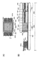
표시장치의 화소의 구성을 도 1에 나타낸다. 도 1(A)는 화소의 평면 구성을 나타낸 상면도이며, 도 1(B)는 화소의 적층구성을 나타낸 단면도이다. 또한, 도 1(A)에서의 A1-A2, B1-B2, C1-C2의 쇄선은 도 1(B)의 단면 A1-A2, 단면 B1-B2, 단면 C1-C2에 각각 상당하는 것이다.The structure of the pixel of a display apparatus is shown in FIG. FIG. 1A is a top view showing a planar configuration of a pixel, and FIG. 1B is a sectional view showing a stacked configuration of a pixel. In addition, the chain line of A1-A2, B1-B2, C1-C2 in FIG. 1 (A) corresponds to the cross section A1-A2, the cross section B1-B2, and the cross section C1-C2 of FIG. 1 (B), respectively.
단면 A1-A2는 화소부에서 사용되는 트랜지스터(151)의 적층구조를 나타내고 있다. 트랜지스터(151)는 하부 게이트 구조의 일 양태이다.Cross sections A1-A2 show the stacked structure of the
또한, 단면 B1-B2는 화소부에 형성되는 용량부의 적층구조를 나타내고 있다.In addition, cross-section B1-B2 has shown the laminated structure of the capacitor | capacitor part formed in a pixel part.
또한, 단면 C1-C2는 게이트 배선과 소스 배선과의 교차부의 적층구조를 나타내고 있다.In addition, cross section C1-C2 has shown the laminated structure of the intersection part of a gate wiring and a source wiring.
트랜지스터(151)는 기판(100) 위에 기초막(101)을, 기초막(101) 위에 제 1 도전층으로 형성되는 게이트 전극(111a)을 가지며, 게이트 전극(111a) 위에 제 1 절연층(102)을 갖는다. 또한, 게이트 전극(111a) 위의 제 1 절연층(102)에 접하게 채널 형성영역을 포함하는 산화물 반도체층(113a)을 갖는다. 또한, 제 2 도전층으로 형성되며, 게이트 전극(111a) 위에 단부를 중첩하고, 산화물 반도체층(113a)에 접하는 제 1 전극(115a)과 제 2 전극(115b)을 갖는다. 또한, 제 1 전극(115a)과 제 2 전극(115b)는 트랜지스터(151)의 소스 전극 또는 드레인 전극으로서 기능한다. 또한, 제 1 전극(115a), 제 2 전극(115b), 제 1 절연층(102), 및 산화물 반도체층(113a) 위에 제 2 절연층(107)을 갖는다. 또한, 제 2 절연층(107) 위에 제 3 절연층(108)을 가지며, 제 3 절연층(108) 위에는 제 2 절연층(107)과 제 3 절연층(108)에 형성한 콘택홀(128)을 통해 제 2 전극(115b)과 접속하는 제 3 도전층으로 형성되는 제 1 화소전극(109)을 갖는다.The
또한, 화소부에 형성되는 용량부는 제 1 도전층으로 형성되는 용량배선(111b)과 제 3 도전층으로 형성되는 제 1 화소전극(109)과의 사이에 제 1 절연층(102), 제 2 절연층(107), 및 제 3 절연층(108)을 개재시킨 구성을 갖는다.The capacitor formed in the pixel portion includes the first insulating
또한, 게이트 배선과 소스 배선의 교차부는 제 1 도전층으로 형성되는 게이트 배선(111c)과 제 2 도전층으로 형성되는 소스 배선(115c)과의 사이에 제 1 절연층(102)과 산화물 반도체층(113b)을 개재시킨 구성으로 하여도 좋다. 산화물 반도체층(113b)을 사이에 개재시킴으로써, 배선간의 거리를 넓혀, 배선의 교차부에 생기는 용량을 저감할 수 있다.In addition, the first insulating
본 실시형태에서는 제 1 도전층에 구리를 사용한다. 또한, 제 1 도전층으로서는 구리를 주성분으로 포함하는 층을 단층으로, 또는 다른 도전층과 적층된 것을 사용할 수 있다. 구리를 주성분으로 포함하는 제 1 도전층은 도전율이 높고, 배선저항을 낮출 수 있다.In this embodiment, copper is used for the first conductive layer. In addition, as a 1st conductive layer, what laminated | stacked the layer which consists of copper as a main component as a single layer, or another conductive layer can be used. The first conductive layer containing copper as a main component has high electrical conductivity and can lower wiring resistance.
또한, 구리를 주성분으로 포함하는 층의 한쪽 또는 양쪽의 면에 접하도록 Cr, Ta, Ti, Mo, W 등의 고융점 금속재료층, 또는 그 금속재료를 성분으로 하는 합금재료를 적층시킨 구성으로 하여도 좋다. 또한, Si, Ti, Ta, W, Mo, Cr, Nd, Sc, Y 등 Al막에 발생하는 힐록(hillock)이나 휘스커(Whisker)의 발생을 방지하는 원소가 첨가되어 있는 Al재료를 사용함으로써 내열성을 향상시키는 것이 가능하게 된다. 또한, 그 도전층은 적어도 가열처리에 견딜 수 있을 정도의 내열성을 갖고 있는 것이 바람직하다.In addition, a high melting point metal material layer such as Cr, Ta, Ti, Mo, W, or an alloy material containing the metal material is laminated so as to contact one or both surfaces of a layer containing copper as a main component. You may also do it. In addition, heat resistance is achieved by using an Al material to which elements such as Si, Ti, Ta, W, Mo, Cr, Nd, Sc, and Y are added to prevent the formation of hillocks or whiskers. It is possible to improve. Moreover, it is preferable that the electrically conductive layer has heat resistance to the grade which can endure at least heat processing.
또한, 구리를 주성분으로 포함하는 층에 겹치도록 예를 들면 질화탄탈막을 형성하여, 구리의 확산을 억제하는 배리어막을 형성하여도 좋다.Further, for example, a tantalum nitride film may be formed so as to overlap a layer containing copper as a main component, and a barrier film for suppressing diffusion of copper may be formed.
또한, 구리를 주성분으로 포함하는 제 1 도전층은 파장 400nm~450nm 부근의 광을 차단한다. 구리를 주성분으로 포함하는 제1 도전층을 사용하여 산화물 반도체층과 중첩하는 게이트 전극(111a)을 형성함으로써, 기판(100)측으로부터 산화물 반도체층에 파장 400nm~450nm 부근의 광이 도달하지 않도록 할 수 있다. 산화물 반도체층은 파장 400nm~450nm 부근의 광에 감도를 갖기 때문에, 구리를 주성분으로서 포함하는 제 1 도전층으로 형성한 게이트 전극(111a)은 산화물 반도체층을 사용한 트랜지스터의 전기 특성, 또는 산화물 반도체층을 사용한 반도체 장치의 동작이 파장 400nm~450nm 부근의 광에 의해 불안정해지는 현상을 방지할 수 있다.Moreover, the 1st conductive layer which contains copper as a main component blocks the light of wavelength 400nm-450nm vicinity. By forming the
또한, 구리를 주성분으로 포함하는 제 1 도전층은 기초막(101)과 제 1 절연층(102)과의 사이에 형성된다.The first conductive layer containing copper as a main component is formed between the
또한, 배선재료는 표시장치가 요구되는 성능에 따라 적절히 선택하면 된다. 예를 들면, 게이트 배선에 비해 높은 전달특성이 요구되는 소스 배선을 포함하는 제 2 도전층만을, Cu를 포함하는 배선으로 하여도 좋다.In addition, the wiring material may be appropriately selected depending on the performance required of the display device. For example, only the second conductive layer including the source wiring that requires higher transfer characteristics than the gate wiring may be a wiring containing Cu.
본 실시형태에서는 기초막(101)에 질화규소(SiNy(y>0))막을 사용한다. 질화규소층을 사용함으로써, 구리를 주성분으로 포함하는 제 1 도전층으로부터 구리가 확산되는 현상을 방지할 수 있다. 또한, 기판(100)으로부터 불순물 원소가 반도체 소자에 확산되는 현상을 방지할 수 있다.In this embodiment, a silicon nitride (SiN y (y> 0)) film is used for the
또한, 기초막(101)과 제 1 절연층(102)은 적어도 질화규소층을 포함하며, 다른 절연층과 적층하여도 좋다. 적층할 다른 절연층으로서는 예를 들면 질화산화규소층, 산화질화규소층, 또는 산화규소층 외에, 알루미늄, 탄탈, 이트륨, 또는 하프늄의 산화물, 질화물, 산화질화물, 또는 질화산화물의 1종 또는 그들 화합물을 적어도 2종 이상 포함하는 화합물층을 사용할 수도 있다.The
특히, 질화규소층에, 질화규소보다 높은 유전율을 갖는 절연막을 조합하여 사용하면, 게이트 절연막으로서의 특성이 향상되기 때문에 바람직하다.In particular, when an insulating film having a higher dielectric constant than silicon nitride is used in combination with the silicon nitride layer, the characteristics as the gate insulating film are improved, which is preferable.
또한, 2개의 질화규소막 사이에 구리를 주성분으로 포함하는 제 1 도전층을 형성함으로써, 구리의 확산을 억제할 수 있다.Further, by forming a first conductive layer containing copper as a main component between two silicon nitride films, diffusion of copper can be suppressed.
또한, 기초막(101)과 제 1 절연층(102)은 스퍼터링법, CVD법 또는 고밀도 플라즈마 CVD법으로 제작한 절연막이 바람직하다.As the
본 실시형태에서는 캐리어 농도가 1×1012cm-3 미만으로 고순도화되며, 넓은 밴드 갭을 갖는 In-Ga-Zn-O 산화물 반도체를 산화물 반도체층에 사용한다.In this embodiment, an In—Ga—Zn—O oxide semiconductor having a high band gap and having a high carrier concentration of less than 1 × 10 12 cm −3 is used for the oxide semiconductor layer.
캐리어 농도가 1×1012cm-3 미만으로 고순도화된 산화물 반도체층을 사용하여 제작되는 트랜지스터는 문턱전압이 양의 값이 되며, 소위 노멀리 오프 특성을 갖는다. 또한, 밴드 갭이 넓은 산화물 반도체를 사용하여 제작되는 트랜지스터는 오프 전류가 작다. 이와 같은 특성의 산화물 반도체를 적용한 트랜지스터의 전기 특성에 대해서는 본 실시형태의 마지막에 상세하게 설명한다.The transistor fabricated using an oxide semiconductor layer having a high carrier concentration of less than 1 × 10 12 cm −3 has a positive threshold voltage and has a so-called normally off characteristic. In addition, a transistor fabricated using an oxide semiconductor having a wide band gap has a low off current. The electrical characteristics of the transistor to which the oxide semiconductor of such a characteristic is applied will be described in detail at the end of the present embodiment.
또한, 산화물 반도체층에 사용하는 산화물 반도체로서는 4원계 금속산화물인 In-Sn-Ga-Zn-O계 산화물 반도체나, 3원계 금속산화물인 In-Ga-Zn-O계 산화물 반도체, In-Sn-Zn-O계 산화물 반도체, In-Al-Zn-O계 산화물 반도체, Sn-Ga-Zn-O계 산화물 반도체, Al-Ga-Zn-O계 산화물 반도체, Sn-Al-Zn-O계 산화물 반도체나, 2원계 금속산화물인 In-Zn-O계 산화물 반도체, Sn-Zn-O계 산화물 반도체, Al-Zn-O계 산화물 반도체, Zn-Mg-O계 산화물 반도체, Sn-Mg-O계 산화물 반도체, In-Mg-O계 산화물 반도체, In-O계 산화물 반도체, Sn-O계 산화물 반도체, Zn-O계 산화물 반도체 등을 사용할 수 있다. 또한, 상기 산화물 반도체층에 산화규소를 포함시켜도 좋다. 산화물 반도체층에 결정화를 저해하는 산화규소(SiOx(X>0)를 포함시킴으로써, 제조 프로세스 중에서 산화물 반도체층의 형성 후에 가열처리한 경우 산화물 반도체층의 결정화를 억제할 수 있다.As the oxide semiconductor used for the oxide semiconductor layer, an In-Sn-Ga-Zn-O-based oxide semiconductor which is a quaternary metal oxide, an In-Ga-Zn-O-based oxide semiconductor which is a ternary metal oxide, or In-Sn- Zn-O-based oxide semiconductor, In-Al-Zn-O-based oxide semiconductor, Sn-Ga-Zn-O-based oxide semiconductor, Al-Ga-Zn-O-based oxide semiconductor, Sn-Al-Zn-O-based oxide semiconductor B) In-Zn-O-based oxide semiconductors, Sn-Zn-O-based oxide semiconductors, Al-Zn-O-based oxide semiconductors, Zn-Mg-O-based oxide semiconductors, and Sn-Mg-O-based oxides as binary metal oxides. Semiconductors, In-Mg-O-based oxide semiconductors, In-O-based oxide semiconductors, Sn-O-based oxide semiconductors, Zn-O-based oxide semiconductors and the like can be used. Further, silicon oxide may be included in the oxide semiconductor layer. By including silicon oxide (SiO x (X> 0)) that inhibits crystallization in the oxide semiconductor layer, crystallization of the oxide semiconductor layer can be suppressed when the heat treatment is performed after the formation of the oxide semiconductor layer in the manufacturing process.
또한, 산화물 반도체층으로서는 InMo3(ZnO)m(m>0)으로 표기되는 박막을 사용할 수 있다. 여기서, M은 Ga, Al, Mn 및 Co 중에서 선택된 하나 또는 복수의 금속원소를 나타낸다. 예를 들면 M으로서, Ga, Ga 및 Al, Ga 및 Mn, 또는 Ga 및 Co 등이 있다. InMo3(ZnO)m(m>0)으로 표기되는 구조의 산화물 반도체막 중, M으로서 Ga를 포함하는 구조의 산화물 반도체를 상기 In-Ga-Zn-O 산화물 반도체라고 부르고, 그 박막을 In-Ga-Zn-O 비단결정막이라고도 부르기로 한다.As the oxide semiconductor layer, a thin film expressed by InMo 3 (ZnO) m (m> 0) can be used. Here, M represents one or a plurality of metal elements selected from Ga, Al, Mn, and Co. Examples of M include Ga, Ga and Al, Ga and Mn, or Ga and Co. In the oxide semiconductor film having a structure represented by InMo 3 (ZnO) m (m> 0), an oxide semiconductor having a structure of Ga as M is referred to as the In-Ga-Zn-O oxide semiconductor, and the thin film is In- It is also referred to as Ga-Zn-O non-single crystal film.
또한, 산화물 반도체층에는 RTA(Rapid Thermal Anneal: 라피드 서멀 어닐링)법 등으로 고온에서 단시간에 탈수 또는 탈수소화 처리를 한 것을 사용한다. 이 가열공정에 의해, 산화물 반도체층의 표층부는 입자 사이즈가 1nm이상 20nm이하의 소위 나노 크리스탈(나노 결정이라고도 표기함)로 구성된 결정영역을 갖게 되며, 기타 부분은 비정질, 또는 비정질 영역 중에 미세결정이 여기저기 흩어져 있는 비정질과 미세결정의 혼합물이 된다. 또한, 나노 결정의 크기는 일 예에 지나지 않으며, 발명이 상기의 수치 범위로 한정 해석되는 것은 아니다.As the oxide semiconductor layer, one which has been subjected to dehydration or dehydrogenation at high temperature for a short time by a rapid thermal annealing (RTA) method or the like is used. By this heating step, the surface layer portion of the oxide semiconductor layer has a crystal region composed of so-called nanocrystals (also referred to as nanocrystals) having a particle size of 1 nm or more and 20 nm or less. It is a mixture of amorphous and microcrystalline scattered here and there. In addition, the size of a nanocrystal is only an example, and invention is not limited to the said numerical range.
이와 같은 구성을 갖는 산화물 반도체층을 사용함으로써, 표층부는 나노 결정으로 구성된 치밀한 결정영역이 존재하기 때문에, 표층부로부터의 수분 재침입이나 산소의 탈리에 의한 N형화를 방지할 수 있다. 그 결과, N형화가 영향을 미치는 전기특성의 열화(劣化), 구체적으로는 오프 전류의 상승을 방지할 수 있다.By using the oxide semiconductor layer having such a structure, since the surface layer portion has a dense crystal region composed of nanocrystals, it is possible to prevent N-type formation by re-infiltration of water from the surface layer portion and desorption of oxygen. As a result, it is possible to prevent deterioration of the electrical characteristics that the N-formation affects, specifically raising of the off current.
또한, 결정 영역은 결정립 이외의 것을 포함하고 있어도 좋다. 또한, 결정립의 결정 구조도 상기에 한정되지 않으며, 다른 결정 구조의 결정립을 포함하고 있어도 좋다. 예를 들면, In-Ga-Zn-O계의 산화물 반도체 재료를 사용할 경우에는 In2Ga2ZnO7의 결정립 뿐만 아니라, InGaZnO4의 결정립 등을 포함하고 있어도 좋다.In addition, the crystal region may include other than crystal grains. The crystal structure of the crystal grains is also not limited to the above, and may include crystal grains of other crystal structures. For example, when using an In-Ga-Zn-O-based oxide semiconductor material, not only In 2 Ga 2 ZnO 7 crystal grains but also InGaZnO 4 crystal grains may be included.
본 실시형태에서는 제 2 도전층에 구리를 사용한다. 또한, 구리를 주성분으로 포함하는 층에 겹치도록 예를 들면 질화탄탈막을 형성하여, 구리의 확산을 억제하는 배리어막을 형성하여도 좋다.In this embodiment, copper is used for a 2nd conductive layer. Further, for example, a tantalum nitride film may be formed so as to overlap a layer containing copper as a main component, and a barrier film for suppressing diffusion of copper may be formed.
또한, 제 2 도전층은 제 1 도전층과 마찬가지로 구리를 주성분으로서 포함하는 층을 적어도 가지며, 단층, 또는 다른 도전층과의 적층이어도 좋다. 구리를 주성분으로 포함하는 제 2 도전층은 도전율이 높으며 배선 저항을 낮출 수 있다.In addition, the second conductive layer has at least a layer containing copper as a main component similarly to the first conductive layer, and may be a single layer or a laminate with another conductive layer. The second conductive layer containing copper as a main component has high electrical conductivity and can lower wiring resistance.
제 2 도전층이 갖는, 구리를 주성분으로 포함하는 층이 산화물 반도체층에 접하는 구성에서는 산화물 반도체층의 고순도화에 필요한 가열처리에 의해, 구리를 주성분으로서 포함하는 층과 산화물 반도체층과의 사이에 구리 산화물이 생성되는 경우가 있다. 구리를 주성분으로서 포함하는 층과 산화물 반도체층과의 사이에 생성된 구리 산화물은 반도체이어서, 산화물 반도체층과 제 2 도전층의 전기적인 접속을 방해하지 않는다.In the structure in which the layer containing copper as a main component of the second conductive layer is in contact with the oxide semiconductor layer, a heat treatment necessary for high purity of the oxide semiconductor layer is provided between the layer containing copper as a main component and the oxide semiconductor layer. Copper oxide may be produced in some cases. The copper oxide produced between the layer containing copper as a main component and the oxide semiconductor layer is a semiconductor and does not prevent the electrical connection between the oxide semiconductor layer and the second conductive layer.
또한, 구리를 주성분으로서 포함하는 층이 산화물 반도체층에 접하는 구성에 서, 구리가 산화물 반도체층으로 확산되는 경우가 있다. 그러나, 실리콘 반도체와는 달리, 산화물 반도체층의 특성은 구리 등으로 대표되는 중원자의 확산에 영향을 잘 받지 않는다.Moreover, copper may diffuse into an oxide semiconductor layer in the structure which the layer containing copper as a main component is in contact with an oxide semiconductor layer. However, unlike silicon semiconductors, the characteristics of the oxide semiconductor layer are not affected by the diffusion of heavy atoms represented by copper or the like.
구리를 주성분으로서 포함하는 층과 산화물 반도체층과의 사이에 다른 도전층을 형성하여 제 2 도전층을 구성할 수도 있다.Another conductive layer may be formed between the layer containing copper as a main component and the oxide semiconductor layer to form a second conductive layer.
구리를 주성분으로 포함하는 층과 산화물 반도체층과의 사이에 형성하는 다른 도전층으로서는 산소 친화성이 높은 금속을 포함하는 재료가 바람직하다. 산소 친화성이 높은 금속으로서는 티탄(Ti), 망간(Mn), 마그네슘(Mg), 지르코늄, 베릴륨, 토륨 등을 들 수 있다. 상기 금속 중 어느 하나 또는 복수 중에서 선택된 금속을 포함하는 재료인 것이 바람직하다. As another conductive layer formed between the layer containing copper as a main component and the oxide semiconductor layer, a material containing a metal having high oxygen affinity is preferable. Titanium (Ti), manganese (Mn), magnesium (Mg), zirconium, beryllium, thorium, etc. are mentioned as a metal with high oxygen affinity. It is preferable that it is a material containing a metal selected from any one or a plurality of the above metals.
산화물 반도체층과 산소 친화성이 높은 도전층을 접하도록 형성하면, 계면 부근의 캐리어 밀도가 증가하고 저저항 영역이 형성되어, 산화물 반도체와 도전층과의 콘택 저항을 저감할 수 있다. 이는 산소 친화성이 높은 도전층이 산화물 반도체층으로부터 산소를 빼냄으로써, 산화물 반도체층과 도전층간의 계면에, 산화물 반도체층 중의 금속이 과잉인 층(복합층이라고도 부름.) 또는 산화된 도전막 중 어느 하나, 또는 그 양쪽이 형성되기 때문이다. When the oxide semiconductor layer and the conductive layer having a high oxygen affinity are formed in contact with each other, the carrier density near the interface increases and a low resistance region is formed, whereby the contact resistance between the oxide semiconductor and the conductive layer can be reduced. This is because a conductive layer having a high oxygen affinity draws oxygen out of the oxide semiconductor layer, so that at the interface between the oxide semiconductor layer and the conductive layer, an excess of metal in the oxide semiconductor layer (also called a composite layer) or an oxidized conductive film This is because either one or both are formed.
예를 들면, In-Ga-Zn-O계의 산화물 반도체층과 티탄막이 접하는 구성에서는 산화물 반도체층과 티탄막에 접하는 계면 부근에, 인듐이 과잉인 층과 산화티탄층이 생성되는 경우가 있다. 또한, 산화물 반도체층과 티탄막에 접하는 계면 부근에, 인듐이 과잉인 층 또는 산화티탄층 중 어느 하나가 생성되는 경우가 있다. In-Ga-Zn-O계 산화물 반도체층으로부터 산소가 결손된 인듐이 과잉인 층은 전기전도도가 높고, 산화물 반도체층과 도전층과의 접촉 저항의 저감을 도모할 수 있다.For example, in the structure where the oxide semiconductor layer and the titanium film of the In—Ga—Zn—O type are in contact with each other, an excess layer of indium and a titanium oxide layer may be formed in the vicinity of the interface between the oxide semiconductor layer and the titanium film. In addition, either of a layer with an indium excess or a titanium oxide layer may be produced in the vicinity of the interface between the oxide semiconductor layer and the titanium film. The layer of excess indium lacking oxygen from the In—Ga—Zn—O-based oxide semiconductor layer has high electrical conductivity and can reduce the contact resistance between the oxide semiconductor layer and the conductive layer.
또한, 산화물 반도체층과 접하는 도전막으로서 티탄, 또는 도전성을 갖는 산화티탄막을 사용하여도 좋다. 그 경우, In-Ga-Zn-O계 산화물 반도체층과 산화티탄막이 접하는 구성에서는 산화물 반도체층과 산화티탄막에 접하는 계면 부근에, 인듐이 과잉인 층이 생성되는 경우가 있다.Titanium or a titanium oxide film having conductivity may be used as the conductive film in contact with the oxide semiconductor layer. In such a case, in a structure in which the In—Ga—Zn—O-based oxide semiconductor layer and the titanium oxide film are in contact with each other, an excess layer of indium may be generated in the vicinity of the interface between the oxide semiconductor layer and the titanium oxide film.
또한, 구리를 주성분으로서 포함하는 층과 산화물 반도체층과의 사이에 형성하는 다른 도전층으로서는 전기음성도가 낮은 금속을 포함하는 도전층이 바람직하다. 전기음성도가 늦은 금속으로서는 티탄, 마그네슘, 이트륨, 알루미늄, 텅스텐, 몰리브덴 등을 들 수 있다. 상기 금속 중 어느 하나 또는 복수를 포함하는 재료인 것이 바람직하다.As another conductive layer formed between the layer containing copper as a main component and the oxide semiconductor layer, a conductive layer containing a metal having low electronegativity is preferable. Titanium, magnesium, yttrium, aluminum, tungsten, molybdenum, etc. are mentioned as a metal with a low electronegativity. It is preferable that it is a material containing any one or multiple of the said metals.
구리를 주성분으로서 포함하는 층과 산화물 반도체층과의 사이에 전기음성도가 낮은 금속을 포함하는 도전층을 형성하고, 산화물 반도체층으로부터 수분, 수소 등의 불순물을 탈리하여, i형(진성 반도체) 또는 i형에 한정되지 않고 가까운 산화물 반도체로 함으로써, 상기 불순물로 인해 문턱전압이 시프트하는 등의 트랜지스터의 특성 열화가 촉진되는 것을 막아 오프 전류를 저감시킬 수 있다.A conductive layer containing a metal having low electronegativity is formed between the layer containing copper as a main component and the oxide semiconductor layer, and impurities such as moisture and hydrogen are removed from the oxide semiconductor layer to form an i-type (intrinsic semiconductor). Alternatively, the oxide semiconductor is not limited to the i-type, and thus, the off-state current can be reduced by preventing the deterioration of the characteristics of the transistor such as the shift of the threshold voltage due to the impurities.
전기음성도가 낮은 금속을 포함하는 도전층에 의해 빨려든 수소, 물 등의 불순물은 전기음성도가 낮은 금속과 화합하기 쉽다. 도전층 중에서 금속과 화학결합을 형성하고 있는 불순물은 금속과의 결합이 안정되어 있어, 한번 도전층 안에 빨려든 후에는 산화물 반도체 안으로 방출되기 어렵다.Impurities such as hydrogen and water sucked by the conductive layer containing the metal with low electronegativity are likely to be combined with the metal with low electronegativity. Impurities that form a chemical bond with a metal in the conductive layer have a stable bond with the metal, and thus are hardly released into the oxide semiconductor after being sucked into the conductive layer.
따라서, 전기음성도가 낮은 금속을 포함하는 도전층에 수소 또는 물 등의 불순물이 포획된 상태가 유지되고 있어, 전기음성도가 낮은 금속을 포함하는 도전층 중의 수소 농도가 산화물 반도체층 중의 수소 농도보다도 높다. 구체적으로는 제 1 전극(115a)과 제 2 전극(115b) 중의 수소 농도가 산화물 반도체층 중의 수소 농도의 1.2배 이상, 바람직하게는 5배 이상이 된다.Therefore, a state in which impurities such as hydrogen or water are trapped in the conductive layer containing the low electronegativity metal is maintained, and the hydrogen concentration in the conductive layer containing the low electronegativity metal is the hydrogen concentration in the oxide semiconductor layer. Higher than Specifically, the hydrogen concentration in the
또한, 도전층 중의 수소 농도는 이차 이온 질량분석법(SIMS: Secondary Ion Mass Spectroscopy)에 의한 측정값을 사용한다.In addition, the hydrogen concentration in a conductive layer uses the measured value by secondary ion mass spectroscopy (SIMS).
여기에서, 산화물 반도체막 및 도전막 중의 수소 농도의 분석에 대해 언급해 둔다. 산화물 반도체막 및 도전막 중의 수소 농도 측정은 이차 이온 질량분석법(SIMS: Secondary Ion Mass Spectroscopy)으로 수행한다. SIMS 분석은 그 원리상, 시료표면 근방이나, 재질이 다른 막과의 적층계면 근방의 데이터를 정확하게 얻는 것이 곤란함이 알려져 있다. 이에, 막 중의 수소 농도의 두께 방향의 분포를 SIMS로 분석할 경우, 수소 농도는 대상이 되는 막이 존재하는 범위에서 극단적인 변동이 없고, 거의 일정한 강도가 얻어지는 영역의 평균값을 채용한다. 또한, 측정 대상이 되는 막의 두께가 작을 경우, 인접하는 막의 영향을 받아, 거의 일정한 강도가 얻어지는 영역을 발견할 수 없는 경우가 있다. 이 경우, 해당 막이 존재하는 영역에서의 최대값, 최소값을 수소 농도로서 채용한다. 게다가, 해당막이 존재하는 영역에서 최대값의 피크, 최소값의 피크가 존재하지 않을 경우, 변곡점의 값을 수소 농도로서 채용한다.Here, the analysis of the hydrogen concentration in the oxide semiconductor film and the conductive film is mentioned. Hydrogen concentration measurement in the oxide semiconductor film and the conductive film is performed by secondary ion mass spectroscopy (SIMS). It is known that SIMS analysis is difficult to accurately obtain data in the vicinity of the sample surface or in the vicinity of a laminated interface with a film having a different material. Therefore, when analyzing the distribution of the thickness direction of the hydrogen concentration in a film | membrane by SIMS, the hydrogen concentration does not have an extreme fluctuation in the range in which the target film exists, and employ | adopts the average value of the area | region where an almost constant intensity is obtained. In addition, when the thickness of the film to be measured is small, it may not be possible to find an area where an almost constant strength is obtained under the influence of the adjacent film. In this case, the maximum value and the minimum value in the region where the film is present are employed as the hydrogen concentration. In addition, when the peak of the maximum value and the peak of the minimum value do not exist in the area | region where the said film exists, the value of an inflection point is employ | adopted as hydrogen concentration.
또한, 전기음성도가 낮은 상기 금속 중 티탄, 몰리브덴, 텅스텐은 산화물 반도체층과의 접촉저항이 낮다. 이 때문에, 산화물 반도체층과의 접촉저항이 낮은 제 1 전극(115a)과 제 2 전극(115b)을 형성하는 것이 가능하게 된다. 또한, 티탄, 몰리브덴, 텅스텐을 산화물 반도체막에 접하는 도전막에 사용함으로써, 산화물 반도체막 중의 불순물을 저감할 수 있다.Further, titanium, molybdenum and tungsten among the metals having low electronegativity have low contact resistance with the oxide semiconductor layer. For this reason, it becomes possible to form the
또한, 구리를 주성분으로서 포함하는 층과 산화물 반도체층과의 사이에 형성하는 다른 도전층으로서는 Al, Cr, Ta, Ti, Mo, W 등의 금속재료, 또는 그 금속재료를 성분으로 하는 합금재료를 사용할 수 있다.As another conductive layer formed between the layer containing copper as a main component and the oxide semiconductor layer, a metal material such as Al, Cr, Ta, Ti, Mo, W, or an alloy material containing the metal material is used. Can be used.
또한, 도전성의 금속산화물을 사용할 수 있다. 도전성의 금속산화물로서는 산화인듐(In2O3), 산화주석(SnO2), 산화아연(ZnO), 산화인듐 산화주석 합금(In2O3-SnO2, ITO라 약칭한다), 산화인듐 산화아연 합금(In2O3-ZnO) 또는 상기 금속산화물 재료에 실리콘 혹은 산화실리콘을 포함시킨 것을 사용할 수 있다.In addition, a conductive metal oxide can be used. Examples of conductive metal oxides are indium oxide (In 2 O 3 ), tin oxide (SnO 2 ), zinc oxide (ZnO), indium tin oxide alloy (abbreviated as In 2 O 3 -SnO 2 , ITO), and indium oxide oxidation Zinc alloys (In 2 O 3 -ZnO) or those containing silicon or silicon oxide in the metal oxide material can be used.
또한, 상술한 도전층은 단층으로 한정되지 않고, 2층 이상의 적층을 사용할 수 있다. 또한, 이 도전막은 적어도 가열처리에 견딜 수 있을 정도의 내열성을 가지고 있는 것이 바람직하다.In addition, the conductive layer mentioned above is not limited to a single | mono layer, Lamination | stacking of two or more layers can be used. In addition, it is preferable that the conductive film has heat resistance at least to withstand the heat treatment.
또한, 구리를 주성분으로서 포함하는 층의 한쪽 또는 양쪽에 Cr, Ta, Ti, Mo, W 등의 고융점 금속층을 적층시킨 구성으로 하여도 좋다. 또한, Si, Ti, Ta, W, Mo, Cr, Nd, Sc, Y 등 Al막에 생성되는 힐록이나 휘스커의 발생을 방지하는 원소가 첨가되어 있는 Al재료를 사용함으로써 내열성을 향상시키는 것이 가능하게 된다.Moreover, you may make it the structure which laminated | stacked high melting metal layers, such as Cr, Ta, Ti, Mo, and W, on one or both of the layer containing copper as a main component. In addition, it is possible to improve the heat resistance by using an Al material to which elements such as Si, Ti, Ta, W, Mo, Cr, Nd, Sc, and Y are added to prevent the generation of hillocks or whiskers. do.
본 실시형태에서는 질화규소(SiNy(y>0))층을 제 2 절연층(107)으로 한다.In this embodiment, the silicon nitride (Si Ny (y> 0)) layer is used as the second insulating
제 2 절연층(107)은 수분이나 수소 이온이나 OH- 등의 불순물을 포함하지 않고, 이들이 외부로부터 침입하는 것을 막는 무기 절연층이다. 질화규소막을 사용함으로써, 구리를 주성분으로서 포함하는 제 1 도전층이나 제 2 도전층으로부터 구리가 확산되는 현상을 방지할 수 있다.The second
본 실시형태에서는 제 1 절연층(102)과 제 2 절연층(107)은 모두 질화규소를 사용하여 형성되어 있다. 또한, 제 1 절연층(102)과 제 2 절연층(107)이 접하는 구성을 가지고 있다. 이와 같이, 동종의 무기 절연층이 서로 접하며 트랜지스터(151)의 주위를 둘러싸는 구조로 함으로써, 트랜지스터의 실링 상태를 보다 양호한 상태로 할 수 있다. 또한, 동종의 무기절연막끼리를 접하는 구조로 할 경우, 상술한 무기 절연막을 사용할 수 있는데, 특히 질화실리콘막은 불순물의 배리어성이 우수하기 때문에 바람직하다.In the present embodiment, both the first insulating
또한, 제 2 절연층(107)은 적어도 질화규소층을 포함하며, 다른 절연층과 적층하여도 좋다. 적층하는 다른 절연층으로서는 산화물 절연층, 산화질화물 절연층, 질화물 절연층, 질화산화물 절연층 등의 무기 절연층을 사용할 수 있다. 예를 들면, 질화산화규소층, 산화질화규소층, 산화규소층 등을 적층하여도 좋다.The second
또한, 산화물 반도체층에 접하게 산화물 절연막을 형성하고, 해당 산화물 절연막에 질화규소(SiNy(y>0))층을 적층하면, 산화물 반도체층에서의 산소의 결손을 저감할 수 있다. 구체적으로는 산화물 반도체층과 접하는 측의 제 2 절연층(107)에 산화규소층(SiOx(x>0))을 형성하고, 이 산화규소층 위에 질화규소층을 적층하여도 좋다. 또한, 구리를 주성분으로서 포함하는 제 2 도전층을 질화규소층으로 덮음으로써, 구리의 확산을 억제할 수 있다.In addition, when an oxide insulating film is formed in contact with the oxide semiconductor layer and a silicon nitride (SiN y (y> 0)) layer is laminated on the oxide insulating film, oxygen deficiency in the oxide semiconductor layer can be reduced. Specifically, a silicon oxide layer (SiO x (x> 0)) may be formed in the second insulating
또한, 산화물 반도체층이 수분이나 수소 이온이나 OH- 등의 불순물로 오염되지않도록, 제 2 절연층(107)은 스퍼터링법으로 형성한 막이 바람직하다.The second
제 3 절연층(108)을 마련할 수 있다. 제 3 절연층(108)은 단층막 또는 적층막으로 형성하고, 하층에 형성된 트랜지스터 등의 구조체에 의한 요철을 평활화함으로써, 평탄한 표면을 형성한다. 제 3 절연층(108)으로서는 예를 들면 폴리이미드, 아크릴수지, 벤조시클로부텐계 수지, 폴리아미드, 에폭시수지 등의 내열성 유기재료를 사용할 수 있다. 또한, 상기 유기재료 외에, 저유전율 재료(low-k 재료), 실록산계 수지, PSG(phosphosilicate glass), BPSG(borophosphosilicate glass) 등을 사용할 수 있다. 또한, 이들 재료로 형성되는 절연막을 복수 적층시킴으로써, 제 3 절연층(108)을 형성하여도 좋다. The third
제 1 화소전극(109)을 트랜지스터와 전기적으로 접속하며, 표시장치의 화소에 사용할 수 있다. 제 1 화소전극(109)은 표시소자의 전극으로서 작용하며, 가시광에 대한 투광성을 갖는 도전막을 사용하여 형성한다.The
투광성을 갖는 도전막으로서는 인듐주석산화물(이하, ITO라고 표시한다), 인듐 아연 산화물, 산화규소를 첨가한 인듐주석산화물 등의 투광성을 갖는 도전성 재료를 사용할 수 있다.As the light-transmitting conductive film, a light-transmitting conductive material such as indium tin oxide (hereinafter referred to as ITO), indium zinc oxide, or silicon oxide added with silicon oxide can be used.
이하에 캐리어 농도가 1×1012cm-3 미만으로 고순도화되며 넓은 밴드 갭을 갖는 산화물 반도체를 산화물 반도체층에 적용하는 의의에 대해 설명한다.Hereinafter, the significance of applying an oxide semiconductor having a high band gap with a high carrier concentration of less than 1 × 10 12 cm −3 to the oxide semiconductor layer will be described.
<산화물 반도체의 진성화><Evolution of Oxide Semiconductors>
산화물 반도체에 있어서, DOS(density of states) 등의 물성 연구는 많이 이루어지고 있는데, 이들 연구는 국소 준위 그 자체를 충분히 줄인다는 사상을 포함하지 않는다. 개시하는 발명의 일 양태에서는 에너지 갭 중의 DOS의 원인일 수 있는 물이나 수소를 산화물 반도체 중으로부터 제거함으로써, 고순도화하여, 진성화(I형화)한 산화물 반도체를 제작한다. 이는 국소 준위 그 자체를 충분히 줄인다는 사위에 입각한 것이다. 그리고, 이로써 매우 뛰어난 공업제품의 제조를 가능하게 하는 것이다.In oxide semiconductors, there are many researches on physical properties such as density of states (DOS), and these studies do not include the idea of sufficiently reducing the local level itself. In one aspect of the disclosed invention, an oxide semiconductor which is highly purified and intrinsic (I-formed) is produced by removing water or hydrogen which may be a cause of DOS in an energy gap from an oxide semiconductor. This is based on the idea of sufficiently reducing the local level itself. This makes it possible to manufacture a very good industrial product.
또한, 수소나 물 등을 제거할 때에는 동시에 산소가 제거되어버리는 일이 있다. 이 때문에, 산소결핍으로 인해 발생하는 금속의 미결합손(dangling bond)에 대해 산소를 공급하고, 산소 결함으로 인한 국소 준위를 감소시킴으로써, 산화물 반도체를 더욱 고순도화, 진성화(i형화)하는 것은 바람직하다. 예를 들면, 채널형성영역에 밀접하게 산소 과잉인 산화막을 형성하고, 200℃~400℃, 대표적으로는 250℃ 정도의 온도 조건에서 열처리를 실시함으로써, 해당 산화막으로부터 산소를 공급하여, 산소 결함으로 인한 국소 준위를 저감시키는 것이 가능하다.In addition, when removing hydrogen, water, or the like, oxygen may be removed at the same time. For this reason, by further supplying oxygen to dangling bonds of metals caused by oxygen deficiency and reducing local levels due to oxygen defects, further increasing the purity and intrinsicity (i-type) of the oxide semiconductor is required. desirable. For example, by forming an oxygen-excess oxide film closely in the channel formation region, and performing a heat treatment at a temperature condition of 200 ° C to 400 ° C, typically about 250 ° C, oxygen is supplied from the oxide film to form an oxygen defect. It is possible to reduce the resulting local level.
산화물 반도체의 특성을 악화시키는 요인은 과잉 수소로 인한 전도대 아래 0.1eV~0.2eV의 준위나, 산소 결손으로 인한 깊은 준위 등에 기인하는 것으로 생각된다. 이들 결함을 없애기 위해, 수소를 철저하게 제거하여 산소를 충분히 공급한다. The deterioration of the characteristics of the oxide semiconductor is thought to be due to the level of 0.1 eV to 0.2 eV under the conduction band due to excess hydrogen, or the deep level due to oxygen deficiency. In order to eliminate these defects, hydrogen is thoroughly removed to supply oxygen sufficiently.
또한, 산화물 반도체는 일반적으로 n형으로 되어 있는데, 개시하는 발명의 일 양태에서는 물이나 수소 등의 불순물을 제거함과 아울러, 산화물 반도체의 구성원소인 산소를 공급함으로써 i형화를 실현한다. 이 점, 실리콘 등과 같이 불순물 원소를 첨가한 i형화가 아니라, 종래에 없는 기술사상을 포함하는 것이라 할 수 있다. The oxide semiconductor is generally n-type, but in one embodiment of the disclosed invention, i-type is realized by removing impurities such as water and hydrogen and supplying oxygen which is a member of the oxide semiconductor. This is not an i-type addition of impurity elements such as silicon, but rather a technical idea that has not existed in the prior art.
<산화물 반도체를 사용한 트랜지스터의 전도기구><Conductor Mechanism of Transistors Using Oxide Semiconductors>
산화물 반도체를 사용한 트랜지스터는 몇 개의 특징을 갖는다. 여기서, 그 전도기구에 대해 도 2~도 5를 사용하여 설명한다. 또한, 이하의 설명에서는 이해를 쉽게 하기 위해 이상적인 상황을 가정하고 있으며, 그 모두가 현실의 모습을 반영하고 있다고는 할 수 없다. 또한, 이하의 설명은 어디까지나 하나의 고찰에 지나지 않으며, 발명의 유효성에 영향을 부여하는 것이 아님을 밝힌다.The transistor using an oxide semiconductor has several features. Here, the conduction mechanism is demonstrated using FIGS. In addition, the following description assumes an ideal situation for easy understanding, and not all of them reflect the reality. In addition, the following description is only one consideration, it turns out that it does not affect the validity of an invention.
도 2는 산화물 반도체를 사용한 역(逆)스태거형 트랜지스터의 단면도이다. 게이트전극(GEI) 위에 게이트 절연층(GI)을 통해 산화물 반도체층(OS)이 형성되며, 그 위에 소스 전극(S) 및 드레인 전극(D)이 형성되어 있다. 또한, 그 위에 절연층을 통해 백 게이트(GE2)가 형성되어 있다.2 is a cross-sectional view of an inverted staggered transistor using an oxide semiconductor. The oxide semiconductor layer OS is formed on the gate electrode GEI through the gate insulating layer GI, and the source electrode S and the drain electrode D are formed thereon. Moreover, the back gate GE2 is formed on it through the insulating layer.
도 3에는 도 2에 나타낸 A-A' 단면에 따른 에너지 밴드도(모식도)를 나타낸다. 도 3(A)는 소스와 드레인간의 전위차를 제로(등전위, VD=VS=0V)로 한 경우를 나타내고 있으며, 도 3(B)는 소스에 비해 드레인의 전위를 높게 한 경우(VD>VS)를 나타내고 있다. 3 shows an energy band diagram (schematic diagram) along the AA 'cross-section shown in FIG. 3 (A) shows the case where the potential difference between the source and the drain is zero (equal potential, V D = V S = 0 V), and FIG. 3 (B) shows the case where the potential of the drain is higher than that of the source (V D). > V S ) is shown.
도 4에는 도 2의 B-B' 단면에 따른 에너지 밴드도(모식도)를 나타낸다. 도 4(A)는 게이트 전극(GEI)에 양의 전압(VG>0)이 부여된 상태이며, 소스와 드레인 사이에 캐리어(전자)가 흐르는 온 상태를 나타내고 있다. 또한, 도 4(B)는 게이트 전극(GEI)에 음의 전압(VG<0)이 인가된 상태이며, 오프 상태(소수 캐리어는 흐르지 않는 상태)인 경우를 나타낸다.4 is an energy band diagram (schematic diagram) taken along the line BB 'of FIG. FIG. 4A shows a state in which a positive voltage V G > 0 is applied to the gate electrode GEI, and an on state in which carriers (electrons) flow between a source and a drain. 4B shows a case where a negative voltage V G <0 is applied to the gate electrode GEI and is in an OFF state (a state in which minority carriers do not flow).
도 5는 진공준위와 금속의 일함수(φM)와의 관계, 및 진공준위와 산화물 반도체의 전자친화력(χ)과의 관계를 나타낸다.5 shows the relationship between the vacuum level and the work function φ M of the metal, and the relationship between the vacuum level and the electron affinity χ of the oxide semiconductor.
상온에서 금속 중의 전자는 축퇴하고 있으며, 페르미 준위(Fermi level)는 전도대 내에 위치한다. 한편, 종래의 산화물 반도체는 n형이며, 그 페르미 준위(EF)는 밴드 갭 중앙에 위치하는 진성 페르미 준위(Ei)로부터 떨어져서 전도대 근처에 위치하고 있다. 또한, 산화물 반도체에서 수소의 일부는 도너가 되어 n형화하는 요인 중 하나인 것이 알려져 있다.At room temperature, the electrons in the metal degenerate, and the Fermi level is located in the conduction band. On the other hand, the conventional oxide semiconductor is n-type, and its Fermi level (E F ) is located near the conduction band away from the intrinsic Fermi level (E i ) located at the center of the band gap. It is also known that a part of hydrogen in the oxide semiconductor is a donor and is one of the factors for n-type formation.
이에 반해, 개시하는 발명의 일 양태에 따른 산화물 반도체는 n형화의 요인인 수소를 산화물 반도체로부터 제거하여, 산화물 반도체의 주성분 이외의 원소(불순물 원소)가 가능한 포함되지 않도록 고순도화함으로써 진성(i형)으로 하거나 또는 진성화하고자 한 것이다. 즉, 불순물 원소를 첨가하여 i형화하는 것이 아니라, 수소나 물 등의 불순물을 가능한 제거함으로써, 고순도화된 i형(진성 반도체) 또는 그에 근접하게 하는 것을 특징으로 하고 있다. 이로써, 페르미 전위(EF)는 진성 페르미 준위(Ei)와 같은 정도로 할 수 있다.On the other hand, the oxide semiconductor according to one aspect of the disclosed invention is intrinsic (i-type) by removing hydrogen, which is a factor of n-type formation, from an oxide semiconductor and making it highly purified so that elements (impurity elements) other than the main component of the oxide semiconductor are not contained as much as possible. ) Or to insult. In other words, the i-type (intrinsic semiconductor) which is highly purified or close to it is characterized by removing impurities such as hydrogen and water as much as possible, rather than adding the impurity element to form i-type. As a result, the Fermi potential E F can be set to the same degree as the intrinsic Fermi level E i .
산화물 반도체의 밴드 갭(Eg)은 3.15eV이고, 전자친화력(χ)은 4.3V라 말해지고 있다. 소스 전극 및 드레인 전극을 구성하는 구리(Cu)의 일함수는 4.6eV로, 산화물 반도체의 전자친화력(χ)보다 약간 낮고, 티탄(Ti)의 일함수는 산화물 반도체의 전자친화력(χ)과 거의 동등하다. 이 경우, 금속-산화물 반도체 계면에서, 전자에 대해 커다란 쇼트 키형 장벽은 형성되지 않는다. The band gap Eg of the oxide semiconductor is 3.15 eV, and the electron affinity χ is said to be 4.3V. The work function of copper (Cu) constituting the source electrode and the drain electrode is 4.6 eV, slightly lower than the electron affinity (χ) of the oxide semiconductor, and the work function of titanium (Ti) is almost equal to the electron affinity (χ) of the oxide semiconductor. Equal In this case, at the metal-oxide semiconductor interface, no large Schottky-type barrier is formed for the electrons.
금속의 일함수(φM)와 산화물 반도체의 전자친화력(χ)이 거의 같은 경우, 양자가 접촉하면 도 3(A)에 나타낸 바와 같은 에너지 밴드도(모식도)가 나타난다.In the case where the work function φ M of the metal and the electron affinity χ of the oxide semiconductor are almost the same, an energy band diagram (schematic diagram) as shown in FIG.
도 3(B)에 있어, 검은 동그라미(●)는 전자를 나타내며, 드레인에 양의 전압(VD>0)을 인가한 후에, 게이트에 전압을 인가하지 않는 경우(VG=0)를 점선으로 나타내고, 게이트에 양의 전압(VG=0)을 인가한 경우를 실선으로 나타낸다. 게이트에 양의 전압(VG>0)을 인가한 경우, 드레인에 양의 전위가 부여되면, 전자는 배리어(h)를 넘어 산화물 반도체로 주입되고 드레인을 향해 흐른다. 배리어의 높이(h)는 게이트 전압과 드레인 전압에 따라 변화하는데, 게이트에 양의 전압((VG>0)을 인가하고 양의 드레인 전압이 인가될 경우에는 전압 인가가 없는 도 3(A)의 배리어 높이(h), 즉 밴드 갭(Eg)의 1/2보다도 배리어의 높이(h)는 낮아진다. 게이트에 전압을 인가하지 않을 경우에는 높은 포텐셜 장벽 때문에, 전극으로부터 산화물 반도체측으로 캐리어(전자)가 주입되지 않고, 전류를 흘리지 않는 오프 상태를 나타낸다. 한편, 게이트에 양의 전압을 인가하면, 포텐셜 장벽이 저하되고 전류를 흘리는 온 상태를 나타낸다.In Fig. 3B, the black circle (동그라미) indicates electrons, and after applying a positive voltage (V D > 0) to the drain, no voltage is applied to the gate (V G = 0). The case where a positive voltage (V G = 0) is applied to the gate is indicated by a solid line. When a positive voltage (V G > 0) is applied to the gate, when a positive potential is applied to the drain, electrons are injected into the oxide semiconductor over the barrier h and flow toward the drain. The height h of the barrier varies depending on the gate voltage and the drain voltage. When the positive voltage ((V G > 0) is applied to the gate and the positive drain voltage is applied, FIG. 3 (A) does not apply voltage. The barrier height h, i.e., the height h of the barrier is lower than half of the band gap E g . When no voltage is applied to the gate, the carrier (electrons) from the electrode to the oxide semiconductor side due to the high potential barrier. ) Is not injected and no current flows in. On the other hand, when a positive voltage is applied to the gate, the potential barrier is lowered and an on state is flowing.
이 때 산화물 반도체에 주입된 전자는 도 4(A)에 나타낸 바와 같이, 게이트 절연층과 고순도화된 산화물 반도체와의 계면 부근(산화물 반도체의 에너지적으로 안정된 최저부)을 이동한다.At this time, the electrons injected into the oxide semiconductor move near the interface between the gate insulating layer and the highly purified oxide semiconductor (energy stabilized lowest portion of the oxide semiconductor).
또한, 도 4(B)에 나타낸 바와 같이, 게이트 전극(GEI)에 음의 전위(역바이어스)가 부여되면, 소수 캐리어인 홀은 실질적으로 제로이기 때문에, 전류는 한정되지 않고 제로에 가까운 값이 된다.In addition, as shown in FIG. 4B, when a negative potential (reverse bias) is applied to the gate electrode GEI, since the hole serving as the minority carrier is substantially zero, the current is not limited and a value close to zero is obtained. do.
이와 같이 산화물 반도체의 주성분 이외의 원소(불순물 원소)가 가능한 포함되지 않도록 고순도화함으로써, 진성(i형)으로 하거나, 또는 실질적으로 진성이 되기 때문에, 게이트 절연층과의 계면특성이 나타나게 된다. 그 때문에, 게이트 절연층에는 산화물 반도체와 양호한 계면을 형성할 수 있는 것이 요구된다. 구체적으로는 예를 들면 VHF대~마이크로파대의 전원 주파수로 생성되는 고밀도 플라즈마를 이용한 CVD법으로 제작되는 절연층이나, 스퍼터링법으로 제작되는 절연층 등을 사용하는 것이 바람직하다.Thus, by making it highly purified so that elements (impurity elements) other than the main component of an oxide semiconductor are contained as possible, it becomes intrinsic (i-type) or becomes substantially intrinsic, and the interface characteristic with a gate insulating layer will appear. Therefore, the gate insulating layer is required to be able to form a good interface with the oxide semiconductor. Specifically, for example, it is preferable to use an insulating layer produced by the CVD method using a high-density plasma generated at a power source frequency of the VHF band to the microwave band, or an insulating layer produced by the sputtering method.
산화물 반도체를 고순도화하면서, 산화물 반도체와 게이트 절연층과의 계면을 양호한 것으로 함으로써, 예를 들면, 트랜지스터의 채널폭(W)이 1×10⁴㎛, 채널 길이(L)가 3㎛인 경우에는 상온에서 10-13A 이하의 오프 전류, 0.1V/dec의 문턱전압 이하에서의 기울기(subthreshold swing)값(S값)(게이트 절연층의 두께 : 100nm)이 실현될 수 있다.By making the interface between the oxide semiconductor and the gate insulating layer good while making the oxide semiconductor highly purified, for example, when the channel width W of the transistor is 1 × 10 4 μm and the channel length L is 3 μm, An off current of 10 −13 A or less at room temperature, and a subthreshold swing value (S value) at a threshold voltage of 0.1 V / dec or less (thickness of the gate insulating layer: 100 nm) can be realized.
이와 같이, 산화물 반도체의 주성분 이외의 원소(불순물 원소)가 가능한 포함되지 않도록 고순도화함으로써, 트랜지스터의 동작을 양호한 것으로 할 수 있다.In this way, the operation of the transistor can be made good by increasing the purity so that elements (impurity elements) other than the main component of the oxide semiconductor are not contained as much as possible.
<산화물 반도체를 사용한 트랜지스터의 핫 캐리어 열화 내성>Hot Carrier Degradation Resistance of Transistors Using Oxide Semiconductors
이어, 산화물 반도체를 사용한 트랜지스터의 핫 캐리어 열화(劣化) 내성에 대해, 도 6~도 8을 사용하여 설명한다. 또한, 이하의 설명에서는 이해를 쉽게 하기 위해 이상적인 상황을 가정하고 있으며, 그 모두가 현실의 모습을 반영하고 있다고는 한정할 수 없다. 또한, 이하의 설명은 어디까지나 하나의 고찰에 지나지않음을 밝힌다.Next, hot carrier deterioration resistance of a transistor using an oxide semiconductor will be described with reference to FIGS. 6 to 8. In addition, the following description assumes an ideal situation for easy understanding, and it cannot be limited that all reflect the state of reality. In addition, the following description reveals only one consideration.
핫 캐리어 열화의 주요인으로서는 채널 핫 일렉트론 주입(CHE 주입)과 드레인 애벌란시(avalanche) 핫 캐리어 주입(DAHC 주입)이 있다. 또한, 이하에서는 간단히 하기 위해 전자만을 고찰한다.The main causes of hot carrier degradation include channel hot electron injection (CHE injection) and drain avalanche hot carrier injection (DAHC injection). In addition, only the former is considered below for simplicity.
CHE 주입이란, 반도체층 중에서 게이트 절연층의 장벽 이상의 에너지를 갖게 된 전자가 게이트 절연층 등에 주입되는 현상을 말한다. 전자로의 에너지 수여는 전자가 저전계로 가속됨으로써 이루어진다.CHE injection refers to a phenomenon in which electrons having energy above the barrier of the gate insulating layer are injected into the gate insulating layer or the like in the semiconductor layer. Conferment of energy to the electrons is achieved by electrons accelerating to a low electric field.
DAHC 주입이란, 고전계로 인해 가속된 전자의 충돌에 의해 에너지를 받은 전자가 게이트 절연층 등에 주입되는 현상을 말한다. DAHC 주입과 CHE 주입과의 차이는 충돌 이온화로 인한 애벌런시 항복을 동반하는지 아닌지에 있다. 또한, DAHC 주입에서는 반도체의 밴드 갭 이상의 운동 에너지를 갖는 전자가 필요로 된다.DAHC injection refers to a phenomenon in which electrons subjected to energy by collision of electrons accelerated by a high electric field are injected into a gate insulating layer or the like. The difference between DAHC injection and CHE injection is whether or not it is accompanied by avalanche yield due to collision ionization. In addition, DAHC injection requires electrons having kinetic energy equal to or greater than the band gap of the semiconductor.
도 6에 실리콘(Si)의 밴드 구조로부터 어림잡은 각종 핫 캐리어 주입에 요하는 에너지를 나타내며, 도 7에는 In-Ga-Zn-O계 산화물 반도체(IGZO)의 밴드 구조로부터 어림잡은 각종 핫 캐리어 주입에 요하는 에너지를 나타낸다. 도 6(A) 및 도 7(A)는 CHE 주입을 나타내며, 도 6(B) 및 도 7(B)는 DAHC 주입을 나타낸다.6 shows energy required for various hot carrier injections estimated from the band structure of silicon (Si), and FIG. 7 shows various hot carrier injections estimated from the band structure of an In—Ga—Zn—O based oxide semiconductor (IGZO). Represents the energy required. 6 (A) and 7 (A) show CHE injection, and FIGS. 6 (B) and 7 (B) show DAHC injection.
실리콘에서는 CHE 주입보다도 DAHC 주입으로 인한 열화가 심각해진다. 이는 실리콘 중에서 충돌하지 않고 가속되는 캐리어(예를 들면 전자)는 극히 조금인 것에 비해, 실리콘은 밴드 갭이 작고 애벌런시 항복이 발생하기 쉬운 것에 기인하고 있다. 애벌런시 항복으로 인해 게이트 절연층의 장벽을 넘을 수 있는 전자의 수는 증가하며, CHE 주입의 확률을 쉽게 웃도는 것이다.In silicon, deterioration due to DAHC injection is more serious than CHE injection. This is due to the fact that silicon has a small band gap and avalanche breakdown is likely to occur, whereas only a small amount of carriers (for example, electrons) are accelerated without colliding in silicon. The avalanche breakdown increases the number of electrons that can cross the barrier of the gate insulation layer, easily exceeding the probability of CHE injection.
In-Ga-Zn-O계 산화물 반도체에서는 CHE 주입에 필요한 에너지는 실리콘의 경우와 크게 다르지 않으며, 역시 그 확률은 낮은 것이다. 또한, DAHC 주입에 필요한 에너지는 밴드 갭의 넓이로 볼 때, CHE 주입에 필요한 에너지와 같은 정도가 된다.In In-Ga-Zn-O-based oxide semiconductors, the energy required for CHE implantation does not differ significantly from that of silicon, and the probability is low. In addition, the energy required for DAHC injection is about the same as the energy required for CHE injection in view of the width of the band gap.
즉, CHE 주입과 DAHC 주입의 확률은 모두 낮으며, 실리콘에 비해 핫 캐리어 열화에 대한 내성은 높다.That is, the probability of both CHE injection and DAHC injection is low and resistance to hot carrier degradation is higher than that of silicon.
그런데, In-Ga-Zn-O계 산화물 반도체의 밴드 갭은 고내압재료로서 주목받는 탄화실리콘(SiC)과 같은 정도이다. 도 8에 4H-SiC에 대한 각종 핫 캐리어 주입에 필요한 에너지를 나타낸다. 또한, 도 8(A)는 CHE 주입을 나타내며, 도 8(B)는 DAHC 주입을 나타낸다. CHE 주입과 관련해서는 In-Ga-Zn-O계 산화물 반도체 쪽이 약간 그 문턱값이 높고 유리하다고 할 수 있다. By the way, the band gap of the In-Ga-Zn-O-based oxide semiconductor is about the same as that of silicon carbide (SiC), which is drawing attention as a high breakdown voltage material. 8 shows the energy required for various hot carrier injections for 4H-SiC. 8 (A) shows CHE injection, and FIG. 8 (B) shows DAHC injection. In terms of CHE implantation, the threshold value of In-Ga-Zn-O-based oxide semiconductor is slightly higher and advantageous.
이상, In-Ga-Zn-O계 산화물 반도체는 실리콘에 비해 핫 캐리어 열화에 대한 내성이나 소스-드레인 파괴에 대한 내성이 매우 높다는 것을 알 수 있다. 또한, 탄화실리콘과 비교해도 손색이 없는 내압이 얻어진다고 할 수 있다.As described above, it can be seen that the In-Ga-Zn-O-based oxide semiconductor has much higher resistance to hot carrier degradation and resistance to source-drain destruction than silicon. In addition, it can be said that a breakdown voltage without inferiority is obtained even in comparison with silicon carbide.
<산화물 반도체를 사용한 트랜지스터에서의 쇼트 채널 효과>Short Channel Effect in Transistors Using Oxide Semiconductors
이어, 산화물 반도체를 사용한 트랜지스터에서의 쇼트 채널 효과에 관해, 도 9 및 도 10을 사용하여 설명한다. 또한, 이하의 설명에서는 이해를 쉽게 하기 위해 이상적인 상황을 가정하고 있으며, 그 모두가 현실의 모습을 반영하고 있다고 는 한정할 수 없다. 또한, 이하의 설명은 어디까지나 하나의 고찰에 지나지 않음을 밝힌다.Next, the short channel effect in the transistor using the oxide semiconductor will be described with reference to FIGS. 9 and 10. In addition, the following description assumes an ideal situation for easy understanding, and not all of them reflect the reality. In addition, the following description reveals only one consideration.
쇼트 채널 효과란, 트랜지스터의 미세화(채널 길이(L)의 축소)에 수반되어 나타나는 전기특성의 열화를 말한다. 쇼트 채널 효과는 드레인의 효과가 소스에까지 미치는 것에 기인하는 것이다. 쇼트 채널 효과의 구체예로서는 문턱전압의 저하, S값의 증대, 누설전류의 증대 등이 있다.The short channel effect refers to the deterioration of electrical characteristics which appears with miniaturization of the transistor (reduction of the channel length L). The short channel effect is due to the effect of the drain on the source. Specific examples of the short channel effect include lowering the threshold voltage, increasing the S value, and increasing the leakage current.
여기에서는 계산결과(디바이스 시뮬레이션)를 사용하여, 쇼트 채널 효과를 억제할 수 있는 구조에 관해 검증하였다. 구체적으로는 캐리어 농도 및 산화물 반도체층의 두께를 다르게 한 4종류의 모델을 준비하여, 채널 길이(L)와 문턱전압(Vth)의 관계를 검토하였다. 모델로서는 하부 게이트 구조의 트랜지스터를 채용하여, 산화물 반도체의 캐리어 농도를 1.7×10⁻⁸/cm3, 또는 1.0×10¹⁵/cm3 중 어느 하나로 하며, 산화물 반도체층의 두께를 1㎛ 또는 30nm 중 어느 하나로 하였다. 또한, 산화물 반도체로서 In-Ga-Zn-O계 산화물 반도체를 채용하고, 게이트 절연층으로서 100nm 두께의 산화질화규소막을 채용하였다. 산화물 반도체의 밴드 갭을 3.15eV, 전자친화력을 4.3eV, 비유전율을 15, 전자이동도를 10cm2/Vs라 가정하였다. 산화질화규소막의 비유전율을 4.0으로 가정하였다. 계산에는 Silvaco사제 디바이스 시뮬레이션 소프트 'Atlas'를 사용하였다.Here, the calculation result (device simulation) was used to verify the structure capable of suppressing the short channel effect. Specifically, four types of models having different carrier concentrations and oxide semiconductor layers were prepared, and the relationship between the channel length L and the threshold voltage Vth was examined. As a model, a transistor having a lower gate structure is employed, and the carrier concentration of the oxide semiconductor is any one of 1.7 × 10 −8 / cm 3 , or 1.0 × 10 15 / cm 3 , and the thickness of the oxide semiconductor layer is 1 μm or 30 nm. Either one. In-Ga-Zn-O-based oxide semiconductors were used as the oxide semiconductor, and a silicon oxynitride film having a thickness of 100 nm was used as the gate insulating layer. It is assumed that the band gap of the oxide semiconductor is 3.15 eV, the electron affinity is 4.3 eV, the relative dielectric constant is 15 and the electron mobility is 10 cm 2 / Vs. The relative dielectric constant of the silicon oxynitride film was assumed to be 4.0. In the calculation, Silvaco device simulation software 'Atlas' was used.
또한, 상부 게이트 구조와 하부 게이트 구조에서는 계산결과에 큰 차이는 없었다.In addition, there was no significant difference in the calculation result between the upper gate structure and the lower gate structure.
계산결과를 도 9 및 도 10에 나타내었다. 도 9는 캐리어 농도가 1.7×10⁻⁸/cm3인 경우, 도 10은 캐리어 농도가 1.0×10¹⁵/cm3인 경우이다. 도 9 및 도 10에는 채널길이(L)가 10㎛인 트랜지스터를 기준으로 하여, 채널길이(L)을 10㎛에서 51㎛까지 변화시켰을 때의 문턱전압(Vth)의 변화량(ΔVth)를 나타내고 있다. 도 9에 나타낸 바와 같이, 산화물 반도체의 캐리어 농도가 1.7×10⁻⁸/cm3 이고 산화물 반도체층의 두께가 1㎛인 경우는 문턱전압(Vth)의 변화량(ΔVth)은 ΔVth=-3.6V이었다. 또한, 도 9에 나타낸 바와 같이, 산화물 반도체의 캐리어 농도가 1.7×10⁻⁸/cm3이고 산화물 반도체층의 두께가 30nm인 경우에는 문턱전압의 변화량(ΔVth)은 ΔVth=-0.2V이었다. 또한, 도 10에 나타낸 바와 같이, 산화물 반도체의 캐리어 농도가 1.0×10¹⁵/cm3이며 산화물 반도체층의 두께가 1㎛인 경우에는 문턱전압의 변화량(ΔVth)은 ΔVth=-3.6V이었다. 또한, 도 10에 나타낸 바와 같이, 산화물 반도체의 캐리어 농도가 1.0×10¹⁵/cm3이며 산화물 반도체층의 두께가 30nm인 경우에는 문턱전압의 변화량(ΔVth)은 ΔVth=-0.2V이었다. 해당 결과는 산화물 반도체를 사용한 트랜지스터에 있어서, 산화물 반도체층의 두께를 얇게 함으로써, 쇼트 채널 효과를 억제할 수 있음을 나타내는 것이라 할 수 있다. 예를 들면, 채널길이가 1㎛ 정도인 경우, 캐리어 농도가 충분히 큰 산화물 반도체층일지라도, 그 두께를 30nm 정도로 하면 쇼트 채널 효과를 충분히 억제할 수 있음이 이해된다.The calculation results are shown in FIGS. 9 and 10. 9 shows a case where the carrier concentration is 1.7 × 10 −8 / cm 3 , and FIG. 10 shows a case where the carrier concentration is 1.0 × 10 15 / cm 3 . 9 and 10 show the change amount ΔVth of the threshold voltage Vth when the channel length L is changed from 10 μm to 51 μm based on a transistor having a channel length L of 10 μm. . As shown in FIG. 9, the carrier concentration of the oxide semiconductor is 1.7 × 10 −8 / cm 3 In the case where the oxide semiconductor layer had a thickness of 1 μm, the change amount ΔVth of the threshold voltage Vth was ΔVth = −3.6V. As shown in FIG. 9, when the carrier concentration of the oxide semiconductor was 1.7 × 10 −8 / cm 3 and the thickness of the oxide semiconductor layer was 30 nm, the variation amount ΔVth of the threshold voltage was ΔVth = −0.2V. As shown in FIG. 10, when the carrier concentration of the oxide semiconductor was 1.0 × 10 15 / cm 3 and the thickness of the oxide semiconductor layer was 1 μm, the change amount (ΔVth) of the threshold voltage was ΔVth = −3.6V. As shown in FIG. 10, when the carrier concentration of the oxide semiconductor was 1.0 × 10 15 / cm 3 and the thickness of the oxide semiconductor layer was 30 nm, the variation amount ΔVth of the threshold voltage was ΔVth = −0.2V. The result indicates that the short channel effect can be suppressed by reducing the thickness of the oxide semiconductor layer in the transistor using the oxide semiconductor. For example, when the channel length is about 1 µm, even if the oxide semiconductor layer has a sufficiently large carrier concentration, it is understood that if the thickness is about 30 nm, the short channel effect can be sufficiently suppressed.
<캐리어 농도에 대해><About carrier density>
개시하는 발명에 따른 기술 사상은 산화물 반도체층에서의 캐리어 농도를 충분히 작게 하여, 가능한 진성(i형)에 가깝게 하고자 하는 것이다. 이하, 캐리어 농도를 구하는 방법, 및 실제로 측정한 캐리어 농도에 관해 도 11 및 도 12를 참조하여 설명한다.The technical idea according to the disclosed invention is to reduce the carrier concentration in the oxide semiconductor layer to be as close as possible to intrinsic (type i). Hereinafter, a method for obtaining a carrier concentration and a carrier concentration actually measured will be described with reference to FIGS. 11 and 12.
먼저, 캐리어 농도를 구하는 방법에 대해 간단하게 설명한다. 캐리어 농도는 MOS 캐패시터를 제작하여 MOS 캐패시터의 CV측정(Capacitance-Voltage measurement)의 결과(CV 특성)를 평가함으로써 구하는 것이 가능하다.First, the method for obtaining the carrier concentration will be briefly described. The carrier concentration can be obtained by fabricating a MOS capacitor and evaluating the results (CV characteristics) of the CV measurement (Capacitance-Voltage measurement) of the MOS capacitor.
보다 구체적으로는 MOS 캐패시터의 게이트 전압(Vg)과 용량(C)과의 관계를 플롯한 C-V 특성을 얻고, 해당 C-V 특성으로부터 게이트 전압(Vg)과 (1/C)2와의 관계를 나타낸 그래프를 취득하여, 해당 그래프의 약반전영역에서의 (1/C)2의 미분값을 구하고, 해당 미분값을 식 (1)에 대입함으로써 캐리어 농도(Nd)의 크기를 구할 수 있다. 또한, 식 (1)에 있어서, e는 전기소량(elementary elctric charge), ε0은 진공 유전율, ε은 산화물 반도체의 비유전율이다.More specifically, a CV characteristic plotting the relationship between the gate voltage (Vg) and the capacitance (C) of the MOS capacitor is obtained, and a graph showing the relationship between the gate voltage (Vg) and (1 / C) 2 from the CV characteristic is shown. The carrier concentration N d can be obtained by acquiring the derivative value of (1 / C) 2 in the weakly inverted region of the graph and substituting the derivative value in equation (1). In Equation (1), e is an elementary elctric charge, ε 0 is a vacuum dielectric constant, and ε is a dielectric constant of an oxide semiconductor.
[수학식 1][Equation 1]
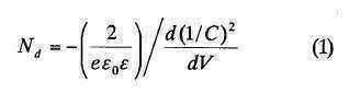
이어, 상기의 방법을 사용하여 실제로 측정한 캐리어 농도에 대해 설명한다. 측정에는 유리 기판위에 티탄막을 300nm의 두께로 형성하고, 티탄막 위에 질화티탄막을 100nm의 두께로 형성하며, 질화티탄막 위에 In-Ga-Zn-O계 산화물 반도체를 사용한 산화물 반도체층을 2㎛의 두께로 형성하고, 산화물 반도체층 위에 산질화규소막을 300nm의 두께로 형성하며, 산질화규소막 위에 은막을 300nm의 두께로 형성한 시료(MOS 캐패시터)를 사용하였다. 또한, 산화물 반도체층은 In, Ga, 및 Zn을 포함하는 금속산화막 타겟(In:Ga:Zn=1:1:0.5[atom%])을 사용한 스퍼터링법에 의해 형성하였다. 또한, 산화물 반도체층의 형성분위기는 아르곤과 산소의 혼합 분위기(유량비는 Ar:O2=30(sccm):15(sccm))로 하였다.Next, the carrier concentration actually measured using the above method will be described. For the measurement, a titanium film was formed on the glass substrate with a thickness of 300 nm, a titanium nitride film was formed on the titanium film with a thickness of 100 nm, and an oxide semiconductor layer using an In—Ga—Zn—O-based oxide semiconductor was formed on the titanium nitride film. The sample (MOS capacitor) which formed in thickness, formed the silicon oxynitride film in thickness of 300 nm on the oxide semiconductor layer, and formed the silver film in the thickness of 300 nm on the silicon oxynitride film was used. In addition, the oxide semiconductor layer was formed by the sputtering method using the metal oxide film target (In: Ga: Zn = 1: 1: 0.5 [atom%]) containing In, Ga, and Zn. In addition, the atmosphere forming the oxide semiconductor layer is a mixed atmosphere of argon and oxygen was set to (flow ratio is Ar: 15 (sccm):
도 11에는 C-V특성을, 도 12에는 Vg와 (1/C)2와의 관계를 각각 나타낸다. 도 12의 약반전영역에서의 (1/C)2의 미분값으로부터 식 (1)을 사용하여 얻어진 캐리어 농도는 6.0×10¹⁰/cm3이었다.FIG. 11 shows CV characteristics, and FIG. 12 shows the relationship between Vg and (1 / C) 2 , respectively. From the derivative of (1 / C) 2 in the weakly inverted region of FIG. 12, the carrier concentration obtained using the formula (1) was 6.0 × 10 10 / cm 3 .
이와 같이, i형화 또는 실질적으로 i형화된 산화물 반도체(예를 들면, 캐리어 농도가 1×10¹²/cm3 미만, 바람직하게는 1×10¹¹/cm3 이하, 더욱 바람직하게는 1.4×10¹⁰/cm3 이하)를 사용함으로써, 매우 뛰어난 오프 전류 특성의 트랜지스터를 얻는 것이 가능하다.As such, the i-typed or substantially i-typed oxide semiconductor (eg, carrier concentration is less than 1 × 10 12 / cm 3 , preferably 1 × 10 11 / cm 3 or less, more preferably 1.4 × 10 10 / cm 3 or less), it is possible to obtain a transistor of very excellent off current characteristics.
본 실시형태에서는 제 1 도전층, 및 제 2 도전층에 구리를 주성분으로서 포함하는 도전층을 사용함으로써, 배선 저항이 저감된 반도체 장치를 제공할 수 있다. 본 실시형태에서 설명한 반도체 장치를 대화면의 표시장치, 고화질의 표시장치에 적용하면, 신호선 종단으로의 신호 전달 지연이나, 전원선의 전압강하 등이 일어나기 어려워지며, 표시 불균일이나 계조 불량 등의 표시품질이 향상된 표시장치를 제공할 수 있다.In this embodiment, a semiconductor device having reduced wiring resistance can be provided by using a conductive layer containing copper as a main component in the first conductive layer and the second conductive layer. When the semiconductor device described in this embodiment is applied to a large-screen display device and a high-quality display device, signal transmission delay to the signal line end, voltage drop of the power supply line, etc. are less likely to occur, and display quality such as display unevenness or gradation defect is poor. It is possible to provide an improved display device.
또한, 캐리어 농도가 1×10¹²/cm-3 미만으로 고순도화된 산화물 반도체층을 사용함으로써, 양의 문턱전압을 가지며, 소위 노멀리 오프 특성의 스위칭 소자를 실현할 수 있다.In addition, by using an oxide semiconductor layer with a high purity at a carrier concentration of less than 1 × 10 12 / cm −3 , a switching element having a positive threshold voltage and a so-called normally off characteristic can be realized.
또한, 2eV를 초과하는 넓은 밴드 갭을 갖는 산화물 반도체를 트랜지스터에 적용함으로써, 오프 전류를 저감할 수 있다. 예를 들면 3.15eV의 밴드 갭을 갖는 In-Ga-Zn-O 산화물 반도체를 사용하여, 채널길이 10㎛인 MOSFET의 역방향 바이어스에서의 누설전류는 1×10-16A/㎛(채널폭 1㎛당) 이하가 된다. 또한, 온 전류와 오프 전류의 비는 1010이상의 충분히 큰 값이 된다.In addition, by applying an oxide semiconductor having a wide band gap of more than 2 eV to the transistor, the off current can be reduced. For example, using an In—Ga—Zn—O oxide semiconductor having a band gap of 3.15 eV, the leakage current at the reverse bias of a MOSFET having a channel length of 10 μm is 1 × 10 -16 A / μm (channel width of 1 μm). Sugar) is as follows. The ratio of the on current to the off current is a sufficiently large value of 10 10 or more.
그 결과, 오프 상태에서 전력을 소비하지 않고, 누설전류도 억제된 전력절약화된 반도체 장치를 제공할 수 있다. 또한, 온 전류와 오프 전류의 비가 큰 반도체 장치를 제공할 수 있다. 또한, 콘트라스트(contrast)가 우수하며 표시 품위가 높은 표시장치를 제공할 수 있다.As a result, it is possible to provide a power-saving semiconductor device in which no leakage current is consumed without consuming power in the off state. In addition, it is possible to provide a semiconductor device having a large ratio of on current and off current. In addition, it is possible to provide a display device having excellent contrast and high display quality.
또한, 고순도화된 산화물 반도체층을 사용함으로써, 전계효과이동도가 높고 고속으로 동작하는 반도체 장치를 제공할 수 있다.In addition, by using the highly purified oxide semiconductor layer, it is possible to provide a semiconductor device having high field effect mobility and operating at high speed.
또한, 구리를 주성분으로서 포함하는 배선을 질화막으로 실링하는 구성을 갖기 때문에, 구리의 확산이 억제되며 신뢰성이 뛰어난 반도체 장치를 제공할 수 있다.Moreover, since it has the structure which seals the wiring which contains copper as a main component with a nitride film, the diffusion of copper is suppressed and the semiconductor device excellent in reliability can be provided.
또한, 본 실시형태는 본 명세서에서 나타낸 다른 실시형태와 적절히 조합할 수 있다.In addition, this embodiment can be combined suitably with the other embodiment shown in this specification.
(실시형태 2)(Embodiment 2)
본 실시형태에서는 본 실시형태 1에서 설명한 반도체 장치의 제작 공정에 대해 도 13(A) 내지 도 13(E)를 참조하여 설명한다. 또한, 도 13(A) 내지 도 13(E)에서의 단면 A1-A2, 단면 B1-B2, 및 단면 C1-C2는 도 1(A)에서의 Al-A2, B1-B2, 및 C1-C2의 쇄선으로 나타낸 부위의 단면도이다.In this embodiment, the manufacturing process of the semiconductor device described in the first embodiment will be described with reference to FIGS. 13A to 13E. Incidentally, the cross sections A1-A2, the cross sections B1-B2, and the cross sections C1-C2 in Figs. 13A to 13E are Al-A2, B1-B2, and C1-C2 in Fig. 1A. It is sectional drawing of the site | part shown by the dashed line.
먼저, 기판(100) 위에 질화규소를 포함하는 기초막(101)을 50nm 이상 300nm 이하, 바람직하게는 100nm 이상 200nm 이하의 두께로 형성한다. 기판(100)은 유리 기판, 세라믹 기판 외에, 본 제작공정의 처리온도에 견딜 수 있을 정도의 내열성을 갖는 플라스틱 기판 등을 사용할 수 있다. 또한, 기판에 투광성을 필요로 하지 않을 경우에는 스테인리스 합금 등의 금속 기판의 표면에 절연막을 형성한 것을 사용하여도 좋다. 유리 기판으로서는 예를 들면 바륨 보로실리케이트 글래스, 알루미노 보로실리케이트 글래스 또는 알루미노 실리케이트 글래스 등의 무알칼리 유리기판을 사용하면 좋다. 그 밖에, 석영 기판, 사파이어 기판 등을 사용할 수도 있다. 또한, 기판(100)으로서, 제 3 세대(550mm×650mm), 제 3.5 세대(600mm×720mm, 또는 620mm×750mm), 제 4 세대(680mm×880mm, 또는 730mm×920mm), 제 5 세대(1100mm×1300mm), 제 6 세대(1500mm×1850mm), 제 7 세대(1870mm×2200mm), 제 8 세대(2200mm×2400mm), 제 9 세대(2400mm×2800mm, 2450mm×3050mm), 제 10 세대(2950mm×3400mm) 등의 유리 기판을 사용할 수 있다.First, a
본 실시형태에서는 기판(100)에 알루미노 보로실리케이트 글래스를 사용한다.In this embodiment, alumino borosilicate glass is used for the
기초막(101)은 질화규소막, 질화산화규소막을 단층 또는 적층하여 형성할 수 있다. 기초막(101)은 스퍼터링법, CVD법, 도포법, 인쇄법 등을 적절히 사용할 수 있다. 또한, 막 중에 인(P)이나 붕소(B)가 도핑되어 있어도 좋다.The
본 실시형태에서는 기초막(101)에 PCVD법으로 성막한 100nm 두께의 질화규소를 사용한다.In this embodiment, silicon nitride having a thickness of 100 nm formed by the PCVD method is used for the
이어, 게이트 전극(111a), 저장 용량배선(111b), 및 게이트 배선(111c)을 형성한다. 먼저, 기초막(101) 위에, 스퍼터링법, 진공증착법, 또는 도금법을 사용하여 100nm 이상 500nm 이하, 바람직하게는 200nm 이상 300nm 이하의 두께로 Cu를 포함하는 제 1 도전층을 형성한다. 이 도전층 위에 포토리소그래피법 또는 잉크젯법 등에 의해 마스크를 형성하고, 이 마스크를 사용하여 제 1 도전층을 에칭하여 게이트 전극(111a), 저장 용량배선(111b), 및 게이트 배선(111c)을 형성한다. 기초막(101)과 제 1 도전층의 밀착성을 개선하기 위해, 기초막(101)에 접하는 제 1 도전층에, W, Ta, Mo, Ti, Cr 등을 사용한 금속층, 또는 이들을 조합한 합금층, 또는 이들 질화물이나 산화물을 형성하여도 좋다.Next, the
또한, 레지스트 마스크를 잉크젯법으로 형성하면, 포토마스크를 사용하지 않기 때문에 제조비용을 저감할 수 있다. 또한, 구리 등의 도전성 나노 페이스트를 잉크젯법에 의해 기판 위에 토출하여 소성함으로써 저렴하게 게이트 전극(111a), 저장 용량배선(111b), 및 게이트 배선(111c)을 형성할 수 있다.In addition, when the resist mask is formed by the inkjet method, the manufacturing cost can be reduced because no photomask is used. In addition, the
본 실시형태에서는 기초막(101) 위에 두께 250nm의 Cu막을 형성하고, 제 1 포토리소그래피 공정으로 형성한 레지스트 마스크를 사용하여 Cu막을 선택적으로 에칭함으로써, 게이트 전극(111a), 저장 용량배선(111b), 및 게이트 배선(111c)을 형성한다.In the present embodiment, a 250 nm thick Cu film is formed on the
그 후, 제 1 절연층(102)을 형성한다. 제 1 절연층(102)은 게이트 절연층으로서 기능하며, 제 1 도전층과 기초막(101) 위에 50nm이상 800nm이하, 바람직하게는 100nm이상 600nm이하의 두께로 형성한다.Thereafter, the first insulating
본 실시형태에서는 스퍼터링법에 의해 제 1 도전층과 기초막(101) 위에 질화규소층(SiNy(y>0))을 성막하여 막두께 100nm의 제 1 절연층(102)을 형성한다.In this embodiment, a silicon nitride layer (SiN y (y> 0)) is formed on the first conductive layer and the
또한, 불순물을 제거함으로써 i형화 또는 실질적으로 i형화된 산화물 반도체(고순도화된 산화물 반도체)는 계면 준위, 계면 전하에 대해 매우 민감하기 때문에, 절연막과의 계면은 중요하다. 그 때문에, 고순도화된 산화물 반도체에 접하는 절연막은 고품질화가 요구된다.In addition, since the i-typed or substantially i-typed oxide semiconductor (highly purified oxide semiconductor) by removing impurities is very sensitive to the interface level and the interface charge, the interface with the insulating film is important. For this reason, the insulating film in contact with the highly purified oxide semiconductor is required to be of high quality.
예를 들면, 마이크로파(2.45GHz)를 사용한 고밀도 플라즈마 CVD는 치밀하고 절연내압이 높은 고품질의 절연막을 형성할 수 있으므로 바람직하다. 고순도화된 산화물 반도체와 고품질 게이트 절연막이 밀접함으로 인해, 계면 준위를 저감하여 계면 특성을 양호한 것으로 할 수 있기 때문이다.For example, high-density plasma CVD using microwaves (2.45 GHz) is preferable because it can form a high quality insulating film with high density and high dielectric breakdown voltage. This is because the interface between the highly purified oxide semiconductor and the high quality gate insulating film can be reduced, thereby making the interface characteristics good.
또한, 고밀도 플라즈마 CVD 장치에 의해 얻어진 절연막은 일정한 두께의 막 형성이 가능하기 때문에 단차피복성이 우수하다. 또한, 고밀도 플라즈마 CVD 장치에 의해 얻어지는 절연막은 얇은 막의 두께를 정밀하게 제어할 수 있다. 또한, 본 명세서에 있어서, 고밀도 플라즈마 CVD 장치는 1×10¹¹/cm3 이상의 플라즈마 밀도를 달성할 수 있는 장치를 가리킨다.In addition, since the insulating film obtained by the high density plasma CVD apparatus can form a film of a constant thickness, the step coverage is excellent. In addition, the insulating film obtained by the high density plasma CVD apparatus can precisely control the thickness of the thin film. In addition, in this specification, the high density plasma CVD apparatus refers to the apparatus which can achieve the plasma density of 1x10 <11> / cm <3> or more.
물론, 게이트 절연막으로서 양질의 절연막을 형성할 수 있는 것이면, 스퍼터링법이나 플라즈마 CVD법 등 다른 성막방법을 적용할 수 있다. 또한, 성막 후의 열처리에 의해 게이트 절연막의 막질, 산화물 반도체와의 계면 특성이 개질되는 절연막이어도 좋다. 어느 경우이든, 게이트 절연막으로서의 막질이 양호함은 물론이며, 산화물 반도체와의 계면준위밀도를 저감하고, 양호한 계면을 형성할 수 있는 것이면 된다.Of course, as long as a good insulating film can be formed as the gate insulating film, other film forming methods such as sputtering and plasma CVD can be applied. Moreover, the insulating film which modifies the film | membrane quality of a gate insulating film and the interface characteristic with an oxide semiconductor by heat processing after film-forming may be sufficient. In any case, the film quality as a gate insulating film is good, of course, and what is necessary is just to be able to reduce the interface state density with an oxide semiconductor, and to form a favorable interface.
이어, 산화물 반도체막(103)을 형성한다. 산화물 반도체막(103)의 두께는 제 1 절연층(102) 위에 5nm이상 200nm이하, 바람직하게는 10nm이상 20nm이하로 한다(도 13(A) 참조).Next, an
본 실시형태에서는 산화물 반도체막으로서, In-Ga-Zn-O계 산화물 반도체 타겟을 사용하여 스퍼터링법에 의해 막두께 15nm의 In-Ga-Zn-O계 비단결정막을 성막한다.In this embodiment, an In—Ga—Zn—O based non-single crystal film having a film thickness of 15 nm is formed by sputtering using an In—Ga—Zn—O based oxide semiconductor target as the oxide semiconductor film.
또한, 산화물 반도체막(103)을 성막하기 전에, 아르곤 가스를 도입하여 플라즈마를 발생시키는 역(逆)스퍼터링를 수행하여, 제 1 절연막(102)의 표면에 부착되어 있는 쓰레기를 제거하는 것이 바람직하다. 역스퍼터링이란, 아르곤 분위기 하에서 기판에 RF 전원을 사용하여 전압을 인가하여 플라즈마를 형성함으로써 표면을 개질하는 방법이다. 또한, 아르곤 분위기 대신에 질소, 헬륨 등을 사용하여도 좋다. 또한, 아르곤 분위기에 산소, N2O 등을 첨가한 분위기에서 실시하여도 좋다. 또한, 아르곤 분위기에 Cl2, CF4 등을 첨가한 분위기에서 수행하여도 좋다. 역스퍼터링 처리 후, 대기에 노출하는 일 없이 산화물 반도체막을 성막으로써, 제 1 절연층(102)과 산화물 반도체막(103)의 계면에 쓰레기나 수분이 부착되는 것을 방지할 수 있다.In addition, before forming the
산화물 반도체막은 실시형태 1에서 든 4원계 금속산화물인 In-Sn-Ga-Zn-O계 산화물 반도체나, 3원계 금속산화물인 In-Ga-Zn-O계 산화물 반도체, In-Sn-Zn-O계 산화물 반도체, In-Al-Zn-O계 산화물 반도체, Sn-Ga-Zn-O계 산화물 반도체, Al-Ga-Zn-O계 산화물 반도체, Sn-Al-Zn-O계 산화물 반도체나, 2원계 금속산화물인 In-Zn-O계 산화물 반도체, Sn-Zn-O계 산화물 반도체, Al-Zn-O계 산화물 반도체, Zn-Mg-O계 산화물 반도체, Sn-Mg-O계 산화물 반도체, In-Mg-O계 산화물 반도체나, In-O계 산화물 반도체, Sn-O계 산화물 반도체, Zn-O계 산화물 반도체 등을 사용할 수 있다. 또한, 상기 산화물 반도체막에 산화규소를 포함시켜도 좋다. 또한, 산화물 반도체막은 앞에서 든 InMO3(ZnO)m(m>0)으로 표기되는 박막을 사용할 수 있다.The oxide semiconductor film is an In-Sn-Ga-Zn-O-based oxide semiconductor as the quaternary metal oxide of
또한, 산화물 반도체막은 희가스(대표적으로는 아르곤) 분위기하, 산소 분위기하, 또는 희가스(대표적으로는 아르곤) 및 산소 분위기하에서 스퍼터링법에 의해 형성할 수 있다. 또한, 스퍼터링법을 사용할 경우, SiO2를 2중량%이상 10중량%이하 포함하는 타겟을 사용하여 성막을 수행하고, 산화물 반도체막에 결정화를 저해하는 SiOx(X>0)을 포함시켜도 좋다.The oxide semiconductor film can be formed by sputtering under a rare gas (typically argon) atmosphere, an oxygen atmosphere, or a rare gas (typically argon) and oxygen atmosphere. In the case of using the sputtering method, film formation may be performed using a target containing 2 wt% or more and 10 wt% or less of SiO 2 , and SiOx (X> 0) may be included in the oxide semiconductor film to inhibit crystallization.
여기에서는 In, Ga, 및 Zn을 포함하는 산화물 반도체 타겟(몰수비가 In2O3:Ga2O3:ZnO=1:1:1, 또는 In2O3:Ga2O3:ZnO=1:1:2)을 사용하여, 기판과 타겟간의 거리를 100mm, 압력 0.6Pa, 직류(DC) 전원 0.5kW, 산소(산소유량비율 100%) 분위기하에서 성막한다. 또한, 펄스 직류(DC) 전원을 사용하면, 쓰레기의 발생을 경감할 수 있으며, 막두께 분포도 작아지기 때문에 바람직하다.Here, an oxide semiconductor target containing In, Ga, and Zn (the molar ratio is In 2 O 3 : Ga 2 O 3 : ZnO = 1: 1: 1, or In 2 O 3 : Ga 2 O 3 : ZnO = 1: 1: 2) is used to form a film between the substrate and the target in an atmosphere of 100 mm, a pressure of 0.6 Pa, a DC power supply of 0.5 kW, and an oxygen (100% oxygen flow rate) atmosphere. In addition, the use of a pulsed direct current (DC) power supply can reduce the generation of waste and is preferable because the film thickness distribution is also reduced.
이 경우에, 처리실 내의 잔류 수분을 제거하면서 산화물 반도체막을 성막하는 것이 바람직하다. 산화물 반도체막에 수소, 수산기를 갖는 물질, 또는 수분이 포함되지 않도록 하기 위함이다.In this case, it is preferable to form an oxide semiconductor film while removing residual moisture in the processing chamber. This is to prevent the oxide semiconductor film from containing hydrogen, a substance having a hydroxyl group, or moisture.
본 실시형태에서 사용하는 멀티 챔버형 스퍼터링 장치는 규소 또는 산화규소(인공석영) 타겟과, 산화물 반도체막의 타겟을 구비하고 있으며, 적어도, 산화물 반도체막용 타겟을 형성한 성막실은 배기수단으로서 크라이오펌프(cryopump)를 갖고 있다. 또한, 크라이오펌프 대신에 터보 분자 펌프를 사용하여, 해당 터보 분자 펌프의 흡기구 위에 수분 등을 흡착시키도록 콜드 트랩(cold trap)을 마련하는 구성으로 하여도 좋다.The multi-chamber sputtering apparatus used in the present embodiment includes a silicon or silicon oxide (artificial quartz) target and a target of an oxide semiconductor film, and at least the film formation chamber in which the target for the oxide semiconductor film is formed is a cryopump (exhaust means). cryopump). A turbo trap may be used in place of the cryopump to provide a cold trap so as to adsorb moisture or the like on the intake port of the turbo pump.
크라이오펌프를 사용하여 배기한 성막실은 예를 들면 수소 원자나 H2O 등 수소 원자를 포함하는 화합물이나, 탄소 원자나 탄소 원자를 포함하는 화합물 등이 배기되기 때문에, 해당 성막실에서 성막한 산화물 반도체막에 포함되는 불순물의 농도를 저감할 수 있다.The deposition chamber exhausted using a cryopump is, for example, a compound containing a hydrogen atom such as a hydrogen atom or H 2 O, or a compound containing a carbon atom or a carbon atom, and the like. The concentration of impurities contained in the semiconductor film can be reduced.
또한, 산화물 반도체막을 제 1 절연층(102) 위에 연속 성막하는 것이 바람직하다.In addition, it is preferable to continuously form an oxide semiconductor film on the first insulating
산화물 반도체막을, 성막할 때에 사용하는 스퍼터링 가스는 수소, 물, 수산기를 갖는 물질, 또는 수소화물 등의 불순물이 농도 ppm 정도, 농도 ppb 정도까지 제거된 고순도 가스를 사용하는 것이 바람직하다.As the sputtering gas used for forming the oxide semiconductor film, it is preferable to use a high purity gas in which impurities such as hydrogen, water, a hydroxyl group, or a hydride have been removed to a concentration ppm or a concentration ppb.
또한, 산화물 반도체막은 기판을 가열하면서 성막하여도 좋다. 이 때 기판 온도를 100℃이상 600℃이하, 바람직하게는 200℃이상 400℃이하로 한다. 기판을 가열하면서 성막함으로써, 성막한 산화물 반도체막에 포함되는 불순물 농도를 저감할 수 있다.The oxide semiconductor film may be formed while heating the substrate. At this time, the substrate temperature is 100 ° C or more and 600 ° C or less, preferably 200 ° C or more and 400 ° C or less. By forming the film while heating the substrate, the impurity concentration contained in the formed oxide semiconductor film can be reduced.
스퍼터링법에는 스퍼터링용 전원에 고주파 전원을 사용하는 RF 스퍼터링법과, DC 스퍼터링법이 있으며, 또한 펄스적으로 바이어스를 부여하는 펄스 DC 스퍼터링법도 있다. RF 스퍼터링법은 주로 절연막을 성막하는 경우에 사용되며, DC 스퍼터링법은 주로 금속도전막을 성막하는 경우에 사용된다.The sputtering method includes an RF sputtering method using a high frequency power source for the sputtering power supply, a DC sputtering method, and a pulsed DC sputtering method for imparting a bias on a pulse basis. The RF sputtering method is mainly used for forming an insulating film, and the DC sputtering method is mainly used for forming a metal conductive film.
또한, 재료가 다른 타겟을 복수 설치할 수 있는 다원 스퍼터링 장치도 있다. 다원 스퍼터링 장치는 동일 챔버에서 다른 재료막을 적층 성막할 수도, 동일 챔버에서 복수 종류의 재료를 동시에 방전시켜 성막할 수도 있다.There is also a multiple sputtering device capable of providing a plurality of targets having different materials. The multiple sputtering apparatus may deposit a different material film in the same chamber or may form a film by simultaneously discharging a plurality of kinds of materials in the same chamber.
또한, 챔버 내부에 자석기구를 구비한 마그네트론 스퍼터링법을 사용하는 스퍼터링 장치나, 글로우 방전을 사용하지 않고 마이크로파를 이용하여 발생시킨 플라즈마를 사용하는 ECR 스퍼터링법을 사용하는 스퍼터링 장치가 있다.Moreover, there exist a sputtering apparatus using the magnetron sputtering method provided with the magnet mechanism inside the chamber, and the sputtering apparatus using the ECR sputtering method using the plasma generated using the microwave without using glow discharge.
또한, 스퍼터링법을 사용하는 성막 방법으로서, 성막 중에 타겟 물질과 스퍼터링 가스 성분을 화학반응시켜 그들 화합물 박막을 형성하는 리액티브 스퍼터링법이나, 성막 중에 기판에도 전압을 거는 바이어스 스퍼터링법도 있다.As the film forming method using the sputtering method, there is also a reactive sputtering method in which a target substance and a sputtering gas component are chemically reacted during film formation to form a thin film of these compounds, or a bias sputtering method that applies a voltage to a substrate during film formation.
이어, 제 2 포토리소그래피 공정을 수행하여 레지스트 마스크를 형성하고, In-Ga-Zn-O계 비단결정막으로 이루어진 산화물 반도체막(103)을 섬 형태로 에칭한다. 에칭에는 예를 들면 구연산이나 옥살산 등의 유기산을 에칭액으로서 사용할 수 있다. 섬 형태의 산화물 반도체층의 단부를 테이퍼 형태로 에칭함으로써, 단차 형위에 따른 배선의 파손을 방지할 수 있다. 또한, 여기에서의 에칭은 습식 에칭에 한정되지 않고 드라이 에칭을 사용하여도 좋다.Next, a resist mask is formed by performing a second photolithography process, and the
이어, 섬 형태의 산화물 반도체층을 형성한 기판에 제 1 가열처리를 실시하여, 섬 형태의 산화물 반도체층의 탈수화 또는 탈수소화를 수행한다.Subsequently, a first heat treatment is performed on the substrate on which the island-shaped oxide semiconductor layer is formed, thereby performing dehydration or dehydrogenation of the island-type oxide semiconductor layer.
또한, 본 명세서에서는 질소, 또는 희가스 등의 불활성기체 분위기하에서의 가열처리를 탈수화 또는 탈수소화를 위한 가열처리라 부른다. 이 가열처리에 의해 H2의 형태로 탈리시키고 있는 것만을 탈수소화라 부르고 있는 것은 아니며, H, OH 등을 탈리하는 것을 포함하여 탈수화 또는 탈수소화라고 편의상 부르기로 한다.In addition, in this specification, heat processing in inert gas atmosphere, such as nitrogen or a rare gas, is called heat processing for dehydration or dehydrogenation. This dehydration in the form of H 2 by the heat treatment is not called dehydrogenation, and is referred to as dehydration or dehydrogenation, including desorbing H, OH and the like.
본 실시형태에서는 제 1 가열처리로서, 섬 형태의 산화물 반도체층을 형성한 기판의 기판 온도를 온도 T로 가열한다. 온도 T는 700℃이하(또는 유리기판의 변형점 이하의 온도), 바람직하게는 350℃이상 500℃이하에서, 제 1 가열처리는 1분간 이상 10분간 이하 정도의 RTA(Rapid Thermal Anneal) 처리로 수행한다.In this embodiment, as a 1st heat processing, the board | substrate temperature of the board | substrate which provided the oxide semiconductor layer of island form is heated to temperature T. As shown in FIG. The temperature T is 700 ° C. or lower (or a temperature below the strain point of the glass substrate), preferably 350 ° C. or higher and 500 ° C. or lower, and the first heat treatment is a rapid thermal annealing (RTA) treatment for 1 minute to 10 minutes. Perform.
제 1 가열처리로서, 기판의 온도를 시간과 함께 도 14(A)에 나타낸 바와 같이 변화시킨다.As the first heat treatment, the temperature of the substrate is changed as shown in Fig. 14A with time.
기간 a-1에서는 기판을 포함하는 분위기를 질소 분위기로 하고, 기판 온도를 T까지 승온하여 유지한 후, 질소 분위기에서 강온한다. 후속의 기간 a-2에서는 처음 기판을 포함하는 분위기를 질소에서 산소 또는 건조공기 분위기로 전환한다. 이어, 기판 온도를 T까지 승온하여 유지한 후, 산소 또는 건조공기 분위기에서 강온한다.In period a-1, after making the atmosphere containing a board | substrate into nitrogen atmosphere, and raising and maintaining a board | substrate temperature to T, it temperature-falls in nitrogen atmosphere. In subsequent periods a-2, the atmosphere comprising the substrate initially is switched from nitrogen to oxygen or dry air atmosphere. Subsequently, after raising and maintaining the substrate temperature to T, the temperature is lowered in oxygen or a dry air atmosphere.
또한, 기간 a-1의 처리와 기간 a-2의 처리를 서로 다른 장치에서 수행하여도 좋다. 서로 다른 장치로 병렬처리함으로써, 공정 시간을 단축할 수 있다.In addition, the processing of the period a-1 and the processing of the period a-2 may be performed by different apparatuses. By parallel processing with different devices, process time can be shortened.
또한, 제 1 가열처리에 있어, 기판의 온도를 시간과 함께 도 14(B)에 나타낸 바와 같이 변화시켜도 좋다.In the first heat treatment, the temperature of the substrate may be changed as shown in Fig. 14B with time.
기판 b-1에서는 기판을 포함하는 분위기를 질소 분위기로 하고, 기판 온도를 T까지 승온하여 유지한다. 후속의 기간 b-2에서는 기판 온도를 T에서 유지하면서, 기판을 포함하는 분위기를 질소로부터 산소 또는 건조공기 분위기로 전환하여, 기판 온도를 T에서 유지한 후, 산소 또는 건조공기 분위기에서 강온하여 좋다.In the board | substrate b-1, the atmosphere containing a board | substrate is made into nitrogen atmosphere, and the board | substrate temperature is raised and maintained to T. In the subsequent period b-2, the substrate-containing atmosphere may be switched from nitrogen to oxygen or dry air atmosphere while the substrate temperature is maintained at T, and the substrate temperature is maintained at T, followed by temperature reduction in oxygen or dry air atmosphere. .
또한, 기간 b-1의 처리와 기간 b-2의 처리를 동일한 장치에서 수행하면, 기판을 이송하는 시간을 단축할 수 있어 바람직하다.In addition, when the processing of the period b-1 and the processing of the period b-2 are performed in the same apparatus, the time for transferring the substrate can be shortened, which is preferable.
제 1 가열처리에 사용하는 불활성가스 분위기로서는 질소, 또는 희가스(헬륨, 네온, 아르곤 등)를 주성분으로 하는 분위기로서, 분위기 중에, 물, 수소 등이 포함되지 않는 것이 바람직하다. 또는, 가열처리장치에 도입하는 불활성 가스의 순도를 6N(99.9999%)이상, 바람직하게는 7N(99.99999%)이상(즉, 불순물 농도를 1ppm이하, 바람직하게는 0.1ppm이하)으로 하는 것이 바람직하다.As an inert gas atmosphere used for a 1st heat processing, it is preferable that nitrogen or a rare gas (helium, neon, argon etc.) is an main component, and water, hydrogen, etc. are not contained in an atmosphere. Alternatively, the purity of the inert gas introduced into the heat treatment apparatus is preferably 6N (99.9999%) or more, preferably 7N (99.99999%) or more (that is, impurity concentration is 1 ppm or less, preferably 0.1 ppm or less). .
또한, 가열처리장치에 도입하는 산소 또는 건조공기는 각각 고순도의 산소가스, 또는 초건조공기(노점이 -40℃이하, 바람직하게는 -60℃이하)로 하는 것이 바람직하다.In addition, the oxygen or dry air introduced into the heat treatment apparatus is preferably high purity oxygen gas or ultra-dry air (dew point is -40 ° C or less, preferably -60 ° C or less).
또한, 산화물 반도체층에 대해 탈수화 또는 탈수소화를 수행할 때는 산화물 반도체층을 대기에 노출시키는 일 없이 물 또는 수소를 재차 혼입시키지 않는 것이 중요하다.In addition, when performing dehydration or dehydrogenation with respect to an oxide semiconductor layer, it is important not to mix water or hydrogen again, without exposing an oxide semiconductor layer to air | atmosphere.
또한, 제 1 가열처리를 수행하는 열처리장치는 전기로나, 가열된 가스 등의 매체로부터의 열전도 또는 열복사에 의해 피처리물을 가열하는 장치여도 좋다. 예를 들면, GRTA(Gas Rapid Thermal Anneal)장치, LRTA(Lamp Rapid Thermal Anneal)장치 등의 RTA(Rapid Thermal Anneal)장치를 사용할 수 있다. LRTA장치는 할로겐 램프, 메탈 할라이드 램프, 크세논 아크 램프, 카본 아크 램프, 고압 나트륨 램프, 고압 수은 램프 등의 램프에서 발하는 광(전자파)의 복사에 의해, 피처리물을 가열하는 장치이다.Further, the heat treatment apparatus for performing the first heat treatment may be an apparatus for heating the object to be processed by heat conduction or heat radiation from a medium such as an electric furnace or a heated gas. For example, a Rapid Thermal Anneal (RTA) device such as a Gas Rapid Thermal Anneal (GRTA) device or a Lamp Rapid Thermal Anneal (LRTA) device may be used. The LRTA apparatus is a device for heating a target object by radiation of light (electromagnetic waves) emitted from lamps such as halogen lamps, metal halide lamps, xenon arc lamps, carbon arc lamps, high pressure sodium lamps, and high pressure mercury lamps.
RTA법을 사용하면, 단시간에 탈수화 또는 탈수소화를 수행할 수 있기 때문에, 유리기판의 변형점을 초과하는 온도에서도 처리할 수 있다. 또한, GRTA장치는 고온을 가스를 사용하여 열처리를 수행하는 장치이다.When the RTA method is used, dehydration or dehydrogenation can be performed in a short time, so that the treatment can be performed even at a temperature exceeding the strain point of the glass substrate. In addition, the GRTA device is a device that performs a heat treatment using a gas at a high temperature.
또한, 가열처리는 이 타이밍에 한정되지 않고, 포토리소그래피 공정이나 성막 공정의 전후 등에서 복수회 실시하여도 좋다.In addition, heat processing is not limited to this timing, You may carry out multiple times before and after a photolithography process, a film-forming process, and the like.
상기 조건에서 탈수화 또는 탈수소화를 충분히 실시한 산화물 반도체층은 승온탈리가스 분석법(TDS:Thermal Desorption Spectroscopy)으로 450℃까지 승온하여도, 수분의 탈리를 나타내는 스펙트럼에서 250∼300℃ 부근에 나타나는 2개의 피크 중 적어도 하나의 피크는 검출되지 않는다.The oxide semiconductor layer sufficiently subjected to dehydration or dehydrogenation under the above conditions, even though the temperature was raised to 450 ° C. by TDS (Thermal Desorption Spectroscopy), was found in the range of 250 to 300 ° C. in the spectrum showing desorption of water. At least one of the peaks is not detected.
또한, 산화물 반도체층은 성막된 단계에서는 대부분의 미결합손을 갖는 비정질이지만, 상기 탈수화 또는 탈수소화 처리의 제 1 가열처리를 실시함으로써, 근거리에 있는 미결합손들끼리 서로 결합하여 질서화된 비정질 구조로 할 수 있다. 또한, 질서화가 발전하면, 비정질영역 중에 미세결정이 여기저기 흩어져 있는 비정질과 미세결정의 혼합물이 형성된다.In addition, although the oxide semiconductor layer is amorphous having most of the unbonded damage in the film formation step, by performing the first heat treatment of the dehydration or dehydrogenation treatment, the unbonded hands in the near distance are bonded to each other and ordered amorphous. It can be made into a structure. Further, when ordering develops, a mixture of amorphous and microcrystals in which microcrystals are scattered in the amorphous region is formed.
또한, 제 1 가열처리의 질소 중의 가열처리에 의해 탈수화 또는 탈수소화와 함께 산소 결핍형이 되며, 산화물 반도체층이 저저항화, 즉 N형화(N-화, N+화 등)된다. 예를 들면, 제 1 가열처리의 질소 중의 가열처리에 의해, 산화물 반도체층은 성막 직후보다도 캐리어 농도가 높아져서, 바람직하게는 1×10¹⁸/cm3이상의 캐리어 농도를 갖는다.In addition, the oxygen deficiency is the type with a dehydration or dehydrogenation by heat treatment in nitrogen of the first heat treatment, the oxide semiconductor layer low resistance, that is, N-type forming - is (N Chemistry, N +, and so on). For example, by the heat treatment in nitrogen of the first heat treatment, the oxide semiconductor layer has a higher carrier concentration than immediately after film formation, and preferably has a carrier concentration of 1 × 10 18 / cm 3 or more.
그러나, N형화(N-화, N+화 등)된 산화물 반도체층은 산소 또는 건조공기 분위기에서 가열, 항온처리되어 산소결손부에 산소가 공급된다. 산소결손부에 산소가 보충된 산화물 반도체층은 고저항화, 즉 I형화된다.However, the N-typed (N - ized, N + -ized, etc.) oxide semiconductor layer is heated and incubated in an oxygen or dry air atmosphere to supply oxygen to the oxygen-deficient portion. An oxide semiconductor layer supplemented with oxygen in an oxygen deficiency portion has a high resistance, that is, an I type.
이와 같은 공정을 거쳐 산화물 반도체층(113a, 113b)은 고순도화된다. 또한, 고순도화된 산화물 반도체층(113a)을 사용하여 제작한 트랜지스터는 양의 문턴 전압을 가지며, 소위 노멀리 오프 특성의 스위칭 소자를 실현할 수 있다.Through this process, the
또한, 트랜지스터의 전기 특성 중, 특히 문턱전압(Vth)은 중요하다. 전계효과이동도가 높아도 문턱전압값이 높거나, 혹은 문터 전압값이 마이너스이면 회로로서 제어하는 것이 곤란하다. 문터 전압값이 높고, 문턱전압의 절대값이 큰 트랜지스터 경우는 구동전압이 낮은 상태에서는 트랜지스터로서의 스위칭 기능을 할 수 없어 부하가 될 우려가 있다.In addition, among the electrical characteristics of the transistor, the threshold voltage Vth is particularly important. Even if the field effect mobility is high, it is difficult to control as a circuit if the threshold voltage value is high or the gate voltage value is negative. In the case where the transistor voltage value is high and the absolute value of the threshold voltage is large, the switching function as the transistor cannot be performed in the state where the driving voltage is low, which may cause a load.
n채널형 트래지스터의 경우, 게이트 전압에 양의 전압을 인가하고 비로소 채널이 형성되어, 드레인 전류가 흐르는 트랜지스터가 바람직하다. 구동전압을 높게 하지 않으면 채널이 형성되지 않는 트랜지스터나, 양의 전압상태에서도 채널이 형성되어 드레인 전류가 흐르는 트랜지스터는 회로에 사용하는 트랜지스터로서는 적합하지 않다. 또한, 트랜지스터의 문턱전압값이 마이너스이면 게이트 전압이 0V이더라도 소스 전극과 드레인 전극 사이에 전류가 흐르는, 소위 노멀리 온(normally on) 특성이 되기 쉽다.In the case of an n-channel transistor, a transistor is formed in which a channel is formed until a positive voltage is applied to the gate voltage so that a drain current flows. If the driving voltage is not increased, a transistor in which a channel is not formed or a transistor in which a channel is formed even in a positive voltage state and a drain current flows is not suitable for a transistor used in a circuit. In addition, if the threshold voltage value of the transistor is negative, even if the gate voltage is 0V, it is likely to become a so-called normally on characteristic in which current flows between the source electrode and the drain electrode.
액티브 매트릭스형 표시장치에서는 회로를 구성하는 트랜지스터의 전기특성이 중요하며, 이 전기특성이 표시장치의 성능을 좌우한다. 트랜지스터를 표시장치에 사용할 경우, 0V에 가능한 가까운 양의 문턱전압을 게이트에 인가하여 채널이 형성되는 것이 표시장치에는 바람직하다.In an active matrix display device, the electrical characteristics of the transistors constituting the circuit are important, and this electrical characteristic determines the performance of the display device. When the transistor is used for a display device, it is preferable for the display device to form a channel by applying a threshold voltage as close as possible to 0V to the gate.
또한, 산화물 반도체층의 제 1 가열처리는 섬 형태의 산화물 반도체층으로 가공하기 전의 산화물 반도체막(103)에 수행할 수도 있다. 그 경우에는 제 1 가열처리 후에, 가열장치로부터 기판을 꺼내어서, 섬 형태의 산화물 반도체층으로 가공하기 위한 포토리소그래피 공정을 수행한다.Further, the first heat treatment of the oxide semiconductor layer may be performed on the
또한, Cu를 포함하는 제 2 도전층을 형성하기 전에, 제 1 절연층(102)을 선택적으로 에칭하여, 제 1 도전층에 이르는 콘택홀을 형성하여도 좋다. 제 1 도전층에 이르는 콘택홀을 형성한 후에 제 2 도전층을 형성하면, 다른 도전층을 개재하는 일 없이 제 1 도전층과 제 2 도전층을 직접 접속할 수 있다. 접속에 필요한 콘택홀의 수를 줄이면, 전기 저항을 작게 할 수 있을 뿐만 아니라, 콘택홀이 점유하는 면적을 작게 할 수 있다.In addition, before forming the second conductive layer containing Cu, the first insulating
이어, Cu를 포함하는 제 2 도전층을 형성한다. Cu를 포함하는 제 2 도전층은 산화물 반도체층(113a, 113b), 및 제 1 절연층위에 스퍼터링법, 진공증착법, 또는 도금법을 사용하여 100nm이상 500nm이하, 바람직하게는 200nm이상 300nm이하의 두께로 형성한다. 이어, 그 도전층 위에 포토리소그래피법 또는 잉크젯법 등에 의해 마스크를 형성하고, 이 마스크를 사용하여 제 2 도전층을 에칭함으로써, 소스 전극 및 드레인 전극으로서 기능하는 제 1 전극(115a), 제 2 전극(115b), 및 소스 배선(115c)을 형성한다.Next, a second conductive layer containing Cu is formed. The second conductive layer containing Cu has a thickness of 100 nm or more and 500 nm or less, preferably 200 nm or more and 300 nm or less, on the
본 실시형태에서는 산화물 반도체층(113a, 113b) 및 제 1 절연막 위에 두께 250nm의 Cu막을 형성하고, 제 3 포토리소그래피 공정으로 형성한 레지스트 마스크를 이용하여 Cu막을 선택적으로 에칭함으로써, 소스 전극 및 드레인 전극이 되는 제 1 전극(115a) 및 제 2 전극(115b), 그리고 소스 배선(115c)을 형성한다.In the present embodiment, a 250 nm thick Cu film is formed over the
또한, 에칭 조건에 따라서도 다르지만, 제 3 포토리소그래피 공정에서 산화물 반도체층의 노출영역이 에칭되는 경우가 있다. 그 경우, 게이트 전극(111a) 위에서 제 1 전극(115a), 또는 제 2 전극(115b)과 겹치는 산화물 반도체층의 두께에 비해, 제 1 전극(115a) 또는 제 2 전극(115b)과 겹치지 않는 산화물 반도체의 두께는 얇아진다(도 13(C) 참조).Also, depending on the etching conditions, the exposed region of the oxide semiconductor layer may be etched in the third photolithography step. In this case, an oxide that does not overlap the
또한, 본 실시형태에서 설명하는 반도체 장치의 제작공정에서 공급하는 열에 의해, 산화물 반도체층에 접하는 Cu막의 면에 구리 산화물이 발생하는데, 구리 산화물은 반도체이기 때문에 전기적인 접속의 장벽이 되지는 않는다.Moreover, although the copper oxide generate | occur | produces on the surface of the Cu film which contact | connects an oxide semiconductor layer by the heat supplied at the manufacturing process of the semiconductor device demonstrated by this embodiment, since copper oxide is a semiconductor, it does not become a barrier of electrical connection.
이어, 제 2 절연층(107)을 형성한다. 제 2 절연층(107)은 적어도 질화규소막을 포함하고, 고순도화된 산화물 반도체층을 오염시키지 않도록, 물, 수소 등의 불순물이 혼입되지 않는 방법(예를 들면 스퍼터링법 등)을 선택하여 사용한다.Next, the second insulating
본 실시형태에서는 제 1 전극(115a) 및 제 2 전극(115b), 소스 배선(115c), 제 1 절연층(102), 그리고 산화물 반도체층에 접하도록, 제 2 절연층(107)으로서 질화규소층(SiNy(y>0))을 형성한다. 질화규소층(SiNy(y>0))은 예를 들면 질화규소 타겟을 희가스(예를 들면 아르곤 가스) 중에서 RF 스퍼터링법을 사용하여 400nm의 두께로 성막한다.In this embodiment, the silicon nitride layer as the second insulating
질화규소막의 스퍼터링법에 의한 성막은 고순도의 가스와, 크라이오펌프를 탑재한 스퍼터링장치를 사용하여 수행한다. 또한, 스퍼터링법으로 형성한 질화물 절연막은 특히 치밀하며, 접하는 층으로 불순물이 확산되는 현상을 억제하는 보호막으로서 단층이어도 이용할 수 있다.The film formation by the sputtering method of a silicon nitride film is performed using the sputtering apparatus equipped with the gas of high purity and a cryopump. Further, the nitride insulating film formed by the sputtering method is particularly dense, and even a single layer can be used as a protective film for suppressing the phenomenon in which impurities diffuse into the contacting layer.
또한, 이 단계에서, 산화물 반도체층과 제 2 절연층(107)이 접하는 영역이 형성된다. 게이트 전극에 중첩하며, 제 1 절연층(102)과 제 2 절연층(107)과의 사이에 끼여 접하는 산화물 반도체층의 영역이 채널형성영역이 된다. 또한, 제 2 절연층(107)은 채널 보호층으로서 기능한다(도 13(D) 참조).In this step, a region where the oxide semiconductor layer and the second insulating
이어, 불활성 가스 분위기하, 또는 산소 분위기하에서 제 2 가열처리를 수행하다. 가열처리의 온도는 200℃이상 400℃이하, 바람직하게는 250℃이상 350℃이하이다. 예를 들면, 질소 분위기하에서 250℃에서 1시간 동안 열처리를 수행하면 된다. 제 2 가열처리를 수행하면, 트랜지스터의 전기적 특성의 편차를 경감할 수 있다. 또한, 본 실시형태에서는 제 2 절연층(107)의 형성 후에 제 2 가열처리를 실시하고 있는데, 제 2 가열처리의 타이밍은 제 1 열처리의 후이면 특별히 한정되지 않는다.Next, a second heat treatment is performed in an inert gas atmosphere or an oxygen atmosphere. The temperature of heat processing is 200 degreeC or more and 400 degrees C or less, Preferably it is 250 degreeC or more and 350 degrees C or less. For example, heat treatment may be performed at 250 ° C. for 1 hour under a nitrogen atmosphere. By performing the second heat treatment, variations in electrical characteristics of the transistor can be reduced. In addition, in this embodiment, although the 2nd heat processing is performed after formation of the 2nd insulating
이어, 제 3 절연층(108)을 형성한다. 제 3 절연층(108)은 50nm이상 300nm이하, 바람직하게는 100nm이상 200nm이하의 두께로 형성한다. 제 3 절연층(108)의 형성법은 특별히 한정되지 않으며, 그 재료에 따라, 스퍼터링법, SOG법, 스핀 코팅, 딥 코팅, 스프레이 코팅, 액적 토출법(잉크젯법, 스크린 인쇄, 오프셋 인쇄 등)을 사용할 수 있다.Next, the third insulating
재료액을 도포하고 베이킹하여 제 3 절연층(108)을 형성할 경우, 산화물 반도체층의 제 2 가열처리(200℃이상 400℃이하, 바람직하게는 250℃이상 350℃이하)를 해당 베이킹 공정에서 실시하여도 좋다. 제 3 절연층(108)의 소성공정과 산화물 반도체층의 어닐링을 겸함으로써 효율적으로 반도체 장치를 제작하는 것이 가능하게 된다.When the material solution is applied and baked to form the third insulating
이어, 제 2 전극(115b)과 제 1 화소전극(109)을 접속하기 위한 콘택홀(128)을 제 2 절연층(107) 및 제 3 절연층(108)에 형성한다. 제 3 절연층(108) 위에 포토리소그래피법 또는 잉크젯법 등에 의해 마스크를 형성하고, 이 마스크를 이용하여 제 2 절연층(107) 및 제 3 절연층(108)을 선택적으로 에칭함으로써 콘택홀을 형성한다. 본 실시형태에서는 제 4 포토리소그래피 공정에서 형성한 레지스트 마스크를 사용하여 제 2 절연층(107) 및 제 3 절연층(108)을 선택적으로 에칭하여 콘택홀(128)을 형성한다.Next, contact holes 128 for connecting the
이어, 제 1 화소전극(109)을 형성한다. 먼저, 제 3 절연층(108), 및 콘택홀(128)을 통해 제 2 전극(115b)에 접하도록, 가시광에 대한 차광성을 갖는 도전막을 30nm이상 200nm이하, 바람직하게는 50nm이상 100nm이하의 두께로 스퍼터링법, 진공증착법 등을 사용하여 형성한다. 이 도전막 위에 포토리소그래피법 또는 잉크젯법 등에 의해 마스크를 형성하고, 이 마스크를 사용하여 상기 도전막을 에칭하여 제 1 화소전극(109)을 형성한다.Next, the
본 실시형태에서는 가시광에 대한 투과성을 갖는 도전막으로서 두께 80nm의 인듐주석산화물(이하, ITO로 나타냄)을 형성하고, 제 5 포토리소그래피공정으로 형성한 레지스트 마스크를 사용하여 가시광에 대한 투광성을 갖는 도전막을 선택적으로 에칭하여 제 1 화소전극(109)을 형성한다(도 13(E) 참조).In this embodiment, a conductive film having a light transmittance to visible light is formed by forming a 80 nm thick indium tin oxide (hereinafter referred to as ITO) as a conductive film having transparency to visible light and using a resist mask formed by a fifth photolithography step. The film is selectively etched to form the first pixel electrode 109 (see Fig. 13E).
또한, 가시광을 투과하는 도전막으로서는 산화텅스텐을 포함하는 인듐 산화물, 산화텅스텐을 포함하는 인듐아연산화물, 산화티탄을 포함하는 인듐산화물, 산화티탄을 포함하는 인듐주석산화물, ITO, 인듐아연산화물, 산화규소를 첨가한 인듐주석산화물 등의 도전성 재료를 사용할 수 있다.Examples of the conductive film that transmits visible light include indium oxide containing tungsten oxide, indium zinc oxide containing tungsten oxide, indium oxide containing titanium oxide, indium tin oxide containing titanium oxide, ITO, indium zinc oxide, and oxidation. Conductive materials, such as indium tin oxide which added the silicon, can be used.
또한, 가시광을 투과하는 도전막을, 도전성 고분자(도전성 폴리머라고도 함)를 포함하는 도전성 조성물을 사용하여 형성할 수 있다. 도전성 조성물을 사용하여 형성한 화소전극은 시트저항이 10000Ω/이하, 파장 550nm에서의 투광율이 70% 이상인 것이 바람직하다. 또한, 도전성 조성물에 포함되는 도전성 고분자의 저항률이 0.1Ω·cm 이하인 것이 바람직하다.Moreover, the electrically conductive film which permeate | transmits visible light can be formed using the electrically conductive composition containing a conductive polymer (also called a conductive polymer). It is preferable that the pixel electrode formed using the conductive composition has a sheet resistance of 10000? / Or less and a light transmittance of 70% or more at a wavelength of 550 nm. Moreover, it is preferable that the resistivity of the conductive polymer contained in a conductive composition is 0.1 ohm * cm or less.
본 실시형태에서는 고순도의 가스와 크라이오펌프 등을 사용하여 수소 원자나, H2O 등의 수소 원자를 포함하는 화합물로 대표되는 불순물을 제거하여 제작한 산화물 반도체층에, 다시 제 1 가열처리를 실시하여 고순도화함으로써, 캐리어 농도가 저감된 산화물 반도체층을 형성할 수 있다. 그 결과, i형화 또는 실질적으로 i형화된 산화물 반도체(예를 들면, 캐리어 농도가 1×10¹²/cm3 미만, 바람직하게는 1×10¹¹/cm3이하)를 사용하여 트랜지스터를 제작하는 것이 가능하게 되어, 매우 뛰어난 오프 전류 특성의 트랜지스터를 제공할 수 있다.In the present embodiment, the first heat treatment is further applied to the oxide semiconductor layer prepared by removing impurities represented by a compound containing a hydrogen atom or a hydrogen atom such as H 2 O using a high purity gas, a cryopump, or the like. By carrying out and making high purity, the oxide semiconductor layer which carrier density was reduced can be formed. As a result, fabricating a transistor using an i-typed or substantially i-typed oxide semiconductor (eg, carrier concentration of less than 1 × 10 12 / cm 3 , preferably 1 × 10 11 / cm 3 or less) This makes it possible to provide a transistor having very excellent off current characteristics.
또한, 본 실시형태에서는 제 1 가열처리의 불활성기체 분위기에서의 탈수화 또는 탈수소화와, 산소 또는 건조공기 분위기에서의 산소 결손부로의 산소 보충이 연속적으로 이루어지기 때문에, 공정시간을 단축할 수 있다.In the present embodiment, the dehydration or dehydrogenation in the inert gas atmosphere of the first heat treatment and the oxygen replenishment to the oxygen-deficient portion in the oxygen or dry air atmosphere are continuously performed, so that the process time can be shortened. .
또한, 본 실시형태는 본 명세서에서 나타낸 다른 실시형태와 적절히 조합할 수 있다.In addition, this embodiment can be combined suitably with the other embodiment shown in this specification.
(실시형태 3)(Embodiment 3)
본 실시형태에서는 실시형태 1과는 다른 구성의 표시장치의 회로 실장 기판의 일 형태를 도 15(A) 및 도 15(B)를 참조하여 설명한다.In this embodiment, one embodiment of a circuit-mounting substrate of a display device having a structure different from that of the first embodiment will be described with reference to FIGS. 15A and 15B.
표시장치의 화소의 구성을 도 15에 나타낸다. 도 15(A)는 화소의 평면 구성을 나타내는 상면도이며, 도 15(B)는 화소의 적층 구성을 나타내는 단면도이다. 또한, 도 15(A)에서의 A1-A2, B1-B2, C1-C2의 쇄선은 도 15(B)에서의 단면 Al-A2, 단면 B1-B2, 단면 C1-C2에 각각 상당하는 것이다.The structure of the pixel of a display apparatus is shown in FIG. Fig. 15A is a top view showing the planar configuration of the pixel, and Fig. 15B is a sectional view showing the lamination configuration of the pixel. In addition, the chain line of A1-A2, B1-B2, C1-C2 in FIG. 15 (A) corresponds to the cross section Al-A2, the cross section B1-B2, and the cross section C1-C2 in FIG.
단면 A1-A2는 화소부에서 사용되는 트랜지스터(152)의 적층구조를 나타내고 있다. 트랜지스터(152)는 하부 게이트 구조의 일 양태이다.Cross sections A1-A2 show the stacked structure of the
또한, 단면 B1-B2는 화소부에 형성되는 용량부의 적층구조를 나타내고 있다.In addition, cross-section B1-B2 has shown the laminated structure of the capacitor | capacitor part formed in a pixel part.
또한, 단면 C1-C2는 게이트 배선과 소스 배선과의 교차부의 적층구조를 나타내고 있다.In addition, cross section C1-C2 has shown the laminated structure of the intersection part of a gate wiring and a source wiring.
본 실시형태에서 예시하는 표시장치의 회로 실장 기판은 실시형태 1에서 예시하는 표시장치의 회로 실장 기판과는 제 1 절연층(102), 제 2 절연층(107), 및 제 2 도전층의 구성이 다르다. 또한, 게이트 배선과 소스 배선과의 교차부의 구성이 다르다.The circuit mounting board of the display device illustrated in the present embodiment is composed of the first insulating
구체적으로는 제 1 절연층(102)은 절연층(102a)과 절연층(102b)이 적층되고, 제 2 절연층(107)은 절연층(107a)과 절연층(107b)이 적층되어 있다. 또한, 제 2 도전층의 구리를 주성분으로서 포함하는 층은 배리어층과 접하는 구성을 갖는다. 또한, 게이트 배선과 소스 배선의 교차부에서, 제 1 도전층으로 형성되는 게이트 배선(111c)과 제 2 도전층으로 형성되는 소스 배선(115c)과의 사이에 제 1 절연층(102)이 개재되어 있다.Specifically, the insulating
본 실시형태에서 예시하는 표시장치의 회로 실장 기판은 실시형태 1에서 예시하는 표시장치의 회로 실장 기판과는 제 1 절연층(102); 제 2 절연층(107); 제 2 도전층의 구리를 구성분으로서 포함하는 층과 접하는 배리어층; 및 게이트 배선과 소스 배선과의 교차부의 구성 이외는 동일하기 때문에, 여기에서는 상세한 설명을 생략한다.The circuit mounting substrate of the display device exemplified in the present embodiment includes a first insulating
본 실시형태에서, 제 1 절연층(102)은 이층으로 이루어진다. 구리를 주성분으로서 포함하는 제 1 도전층과 기초막(101)에 접하는 쪽의 절연층(102a)에 질화규소(SiNy(y>0))층을 사용하고, 산화물 반도체층에 접하는 쪽의 절연층(102b)에 산화규소(SiOx(x>0))층을 사용한다. 제 1 절연층(102)의 막두께는 100nm으로 한다.In this embodiment, the 1st insulating
제 1 절연층(102)은 게이트 절연층으로서 기능하며, 제 1 도전층과 기초막(101) 위에 50nm이상 800nm이하, 바람직하게는 100nm이상 600nm이하의 두께로 형성한다.The first insulating
기초막(101)과 절연층(102a)의 두 질화규소막 사이에, 구리를 주성분으로서 포함하는 제 1 도전층을 형성함으로써, 구리의 확산을 억제할 수 있다.Diffusion of copper can be suppressed by forming the 1st conductive layer which contains copper as a main component between the two silicon nitride films of the
또한, 불순물을 제거함으로써 i형화 또는 실질적으로 i형화된 산화물 반도체(고순도화된 산화물 반도체)는 계면 준위, 계면 전하에 대해 매우 민감하기 때문에, 절연막과의 계면은 중요하다. 그 때문에, 고순도화된 산화물 반도체에 접하는 절연층(102b)은 고품질화가 요구된다.In addition, since the i-typed or substantially i-typed oxide semiconductor (highly purified oxide semiconductor) by removing impurities is very sensitive to the interface level and the interface charge, the interface with the insulating film is important. Therefore, the insulating
예를 들면, μ파(2.45GHz)를 사용한 고밀도 플라즈마 CVD는 치밀하고 절연내압이 높은 고품질의 절연막을 형성할 수 있으므로 바람직하다. 고순도화된 산화물 반도체와 고품질 게이트 절연막이 서로 밀접함으로 인해, 계면 준위를 저감하여 계면 특성을 양호한 것으로 할 수 있기 때문이다.For example, high-density plasma CVD using µ waves (2.45 GHz) is preferable because it can form a high quality insulating film with high density and high dielectric breakdown voltage. This is because the highly purified oxide semiconductor and the high quality gate insulating film are in close contact with each other, whereby the interface level can be reduced and the interface property can be made good.
또한, 고밀도 플라즈마 CVD 장치에 의해 얻어진 절연막은 일정한 두께의 막 형성이 가능하기 때문에 단차피복성이 뛰어나다. 또한, 고밀도 플라즈마 CVD장치에 의해 얻어지는 절연막은 얇은 막의 두께를 치밀하게 제어할 수 있다.In addition, the insulating film obtained by the high-density plasma CVD apparatus is capable of forming a film of a constant thickness, and thus has excellent step coverage. Further, the insulating film obtained by the high density plasma CVD apparatus can precisely control the thickness of the thin film.
물론, 게이트 절연막으로서 양질의 절연막을 형성할 수 있는 것이면, 스퍼터링법이나 플라즈마 CVD법 등 다른 성막방법을 적용할 수 있다. 또한, 성막 후의 열처리에 의해 게이트 절연막의 막질, 산화물 반도체와의 계면 특성이 개질되는 절연막이어도 좋다. 어느 경우이든, 게이트 절연막으로서의 막질이 양호한 것은 물론이며, 산화물 반도체와의 계면준위밀도를 저감하고 양호한 계면을 형성할 수 있는 것이면 된다.Of course, as long as a good insulating film can be formed as the gate insulating film, other film forming methods such as sputtering and plasma CVD can be applied. Moreover, the insulating film which modifies the film | membrane quality of a gate insulating film and the interface characteristic with an oxide semiconductor by heat processing after film-forming may be sufficient. In any case, it is a matter of course that the film quality as a gate insulating film is good, and what is necessary is just to be able to reduce the interface state density with an oxide semiconductor, and to form a favorable interface.
본 실시형태에서는 절연층(102b)을 고밀도 플라즈마 CVD장치(본 명세서에 있어서, 고밀도 플라즈마 CVD장치는 1×10¹¹/cm3 이상의 플라즈마 밀도를 달성할 수 있는 장치를 가리킴)에 의해 수행할 경우, 예를 들면 3kW~6kW의 마이크로파 전력을 인가하여 플라즈마를 발생시켜 절연막을 성막한다.In the present embodiment, when the insulating
챔버에 재료가스로서 모노실란가스(SiH4)와 아산화질소(N2O)와 희가스를 도입하고, 10Pa~30Pa의 압력하에서 고밀도 플라즈마를 발생시켜, 유리 등의 절연 표면을 갖는 기판 위에 절연막을 형성한다. 그 후, 모노실란가스의 공급을 정지하여, 대기에 노출하는 일 없이 아산화질소(N2O)와 희가스를 도입하여 절연막 표면에 플라즈마처리를 실시하여도 된다. 적어도 아산화질소(N2O)와 희가스를 도입하여 절연막 표면에 이루어지는 플라즈마 처리는 절연막의 성막보다 뒤에 수행한다. 상기 프로세스 순서를 거친 절연막은 막두께가 얇고, 예를 들면 100nm미만일지라도 신뢰성을 확보할 수 있는 절연막이다.Monosilane gas (SiH 4 ), nitrous oxide (N 2 O), and rare gas are introduced into the chamber, and a high density plasma is generated under a pressure of 10 Pa to 30 Pa to form an insulating film on a substrate having an insulating surface such as glass. do. Thereafter, the supply of monosilane gas may be stopped, and nitrous oxide (N 2 O) and rare gas may be introduced and plasma treatment may be performed on the surface of the insulating film without exposing to the atmosphere. Plasma treatment performed on the surface of the insulating film by introducing at least nitrous oxide (N 2 O) and a rare gas is performed after film formation of the insulating film. The insulating film which has passed through the above process sequence is an insulating film that is thin and has a reliability even if it is less than 100 nm, for example.
절연막(102b)의 형성시, 챔버에 도입하는 모노실란가스(SiH4)와 아산화질소(N2O)와의 유량비는 1:10~1:200의 범위로 한다. 또한, 챔버에 도입하는 희가스로서는 헬륨, 아르곤, 크립톤, 크세논 등을 사용할 수 있는데, 그 중에서도 저렴한 아르곤을 사용하는 것이 바람직하다.When the insulating
또한, 고밀도 플라즈마장치에 의해 얻어진 절연막은 일정한 두께의 막형성이 가능하기 때문에 단차피복성이 뛰어나다. 또한, 고밀도 플라즈마장치에 의해 얻어지는 절연막은 얇은 막의 두께를 정밀하게 제어할 수 있다.In addition, the insulating film obtained by the high-density plasma apparatus can form a film of a constant thickness, and thus has excellent step coverage. In addition, the insulating film obtained by the high density plasma apparatus can precisely control the thickness of the thin film.
상기 프로세스 순서를 거친 절연막은 종래의 평행평판형 PCVD장치로 얻어지는 절연막과는 크게 다르며, 동일한 에칭액을 사용하여 에칭속도를 비교한 경우, 평행평판형 PCVD장치로 얻어지는 절연막의 10%이상 또는 20%이상 느리다. 따라서, 고밀도 플라즈마장치로 얻어지는 절연막은 치밀한 막이라 할 수 있다.The insulating film that has undergone the above process sequence is significantly different from the insulating film obtained by the conventional parallel flat PCVD apparatus, and when the etching rates are compared using the same etching solution, it is 10% or more or 20% or more of the insulating film obtained by the parallel flat PCVD apparatus. slow. Therefore, the insulating film obtained by the high density plasma apparatus can be called a dense film.
또한, 절연층(102b)으로서는 유기실란가스를 사용한 CVD법에 의해 산화실리콘층을 형성하는 것도 가능하다. 유기실란가스로서는 규산에틸(TEOS: 화학식 Si(OC2H5)4), 테트라메틸실란(TMS: 화학식 Si(CH3)4), 테트라메틸시클로테트라실록산(TMCTS), 옥타메틸시클로테트라실록산(OMCTS), 헥사메틸디실라잔(HMDS), 트리에톡시실란(SiH(OC2H5)3), 트리스디메틸아미노실란(SiH(N(CH3)2)3) 등의 실리콘 함유 화합물을 사용할 수 있다.As the insulating
본 실시형태에서는 제 2 도전층의 구리를 주성분으로서 포함하는 층은 배리어층과 접하는 구성을 가지며, 배리어층으로서 도전성의 금속질화물인 질화탄탈을 사용한다. 구체적으로는 제 2 도전층으로 형성한 제 1 전극(115a), 제 2 전극(115b), 및 소스 배선(115c)은 질화탄탈 사이에 구리를 주성분으로 포함하는 층을 적층한 구성을 갖는다.In this embodiment, the layer containing copper of a 2nd conductive layer as a main component has the structure which contact | connects a barrier layer, and uses tantalum nitride which is electroconductive metal nitride as a barrier layer. Specifically, the
배리어층은 구리의 확산을 억제하는 재료를 사용하여 형성하면 되며, 특히 금속질화물이 바람직하다. 또한, 구리를 주성분으로서 포함하는 층과 접하는 제 1 절연층(102), 또는 제 2 절연층(107)이 금속질화물이면, 이들이 배리어층을 겸하는 구조로 하여도 좋다.What is necessary is just to form a barrier layer using the material which suppresses diffusion of copper, and metal nitride is especially preferable. Moreover, as long as the 1st insulating
특히, 산화물 반도체층(113a)과 접하는 배리어층은 도전성을 갖는 금속질화물을 사용한다. 예를 들면, 질화티탄, 질화탄탈, 질화텅스텐 등을 배리어층에 사용할 수 있다. 도전성을 갖는 배리어층을 통해 산화물 반도체층(113a)과 제 2 도전층의 구리를 주성분으로서 포함하는 층과를 적층함으로써, 구리의 확산을 억제하면서, 산화물 반도체층(113a)과 제 2 도전층의 구리를 주성분으로서 포함하는 층과를 전기적으로 접속할 수 있다.In particular, the barrier layer in contact with the
제 2 도전층의 배리어층을 산화물 반도체층(113a), 및 제 1 절연층(102) 위에 성막하고, 이 배리어층에 접하도록 구리를 주성분으로서 포함하는 층을 성막한다. 또한, 제 2 도전층은 스퍼터링법, 진공증착법, 또는 도금법 등을 사용하여, 100nm이상 500nm이하, 바람직하게는 200nm이상 300nm이하의 두께로 형성한다.A barrier layer of the second conductive layer is formed on the
이어, 제 2 도전층 위에 포토리소그래피법 또는 잉크젯법 등에 의해 마스크를 형성하고, 이 마스크를 이용하여 에칭함으로써, 소스 전극 및 드레인 전극으로서 기능하는 제 1 전극(115a), 제 2 전극(115b), 및 소스 배선(115c)을 형성한다.Subsequently, a mask is formed on the second conductive layer by a photolithography method, an inkjet method, or the like, and is etched using the mask to thereby serve as a
본 실시형태에서는 제 2 절연층(107)을 절연층(107a)과 절연층(107b)의 적층구조로 한다. 제 2 도전층의 배리어층 및 산화물 반도체층에 접하는 절연층(107a)을 산화규소(SiOx(x>0))층으로 형성하고, 절연층(107a)에 접하는 절연층(107b)을 두께 400nm의 질화규소(SiNy(y>0))층으로 형성한다.In this embodiment, the 2nd insulating
제 2 절연층(107)은 고순도화된 산화물 반도체층을 오염시키지 않도록, 물, 수소 등의 불순물이 혼입되지 않는 방법(예를 들면 스퍼터링법 등)을 선택하여 사용한다.The second
절연층(107a)은 순도가 6N이며, 주상(柱狀) 다결정 B 도핑의 규소 타겟(저항값 0.01Ωcm)을 사용하여, 기판과 타겟간의 거리(T-S간 거리)를 89mm, 압력 0.4Pa, 직류(DC) 전원 6kW, 산소(산소유량비율 100%) 분위기하에서 펄스 DC 스퍼터링법에 의해 성막한다. 막두께는 300nm으로 한다.The insulating
성막시의 기판 온도는 실온이상 300℃이하로 하면 되며, 본 실시형태에서는 100℃로 한다.The substrate temperature at the time of film formation should just be room temperature or more and 300 degrees C or less, and is 100 degreeC in this embodiment.
산화규소층의 스퍼터링법에 의한 성막은 고순도의 가스와, 크라이오펌프를 탑재한 스퍼터링장치를 사용하여 수행한다. 또한, 희가스(대표적으로는 아르곤) 분위기하, 산소 분위기하, 또는 희가스(대표적으로는 아르곤) 및 산소 분위기하에서 수행할 수 있다. 또한, 스퍼터링법으로 형성한 산화물 절연막은 특히 치밀하며, 접하는 층으로 불순물이 확산되는 현상을 억제하는 보호막으로서 단층이어도 이용할 수 있다.The film formation by the sputtering method of a silicon oxide layer is performed using the sputtering apparatus equipped with the gas of high purity and a cryopump. It may also be carried out under a rare gas (typically argon) atmosphere, under an oxygen atmosphere, or under a rare gas (typically argon) and oxygen atmosphere. Further, the oxide insulating film formed by the sputtering method is particularly dense, and even a single layer can be used as a protective film for suppressing the phenomenon in which impurities diffuse into the contacting layer.
또한, 타겟으로서 산화규소 타겟 또는 규소 타겟을 사용할 수 있다. 또한, 인(P)이나 붕소(B)를 도핑한 타겟을 사용하며, 산화물 절연막에 인(P)이나 붕소(B)를 첨가할 수도 있다.Moreover, a silicon oxide target or a silicon target can be used as a target. In addition, a target doped with phosphorus (P) or boron (B) may be used, and phosphorus (P) or boron (B) may be added to the oxide insulating film.
또한, 산화물 반도체층에 접하는 절연층(107a)에 산화물 절연막을 형성할 경우, 예를 들면 1nm이상의 막두께의 산화규소(SiOx(x>0))층을 형성할 경우, 규소 타겟이 바람직하다. 규소 타겟을 사용하여, 산소, 및 희가스 분위기하에서 스퍼터링법에 의해 성막한 산화규소막은 규소 원자 또는 산소 원자의 미결합손(댕글링 본드)을 많이 포함하고 있다.In the case where an oxide insulating film is formed in the insulating
산화물 반도체층에 잔존하는 불순물은 규소 원자 또는 산소 원자의 미결합손(댕글링 본드)을 많이 포함하는 절연층(107a)으로 확산되어 고정화된다. 구체적으로는 산화물 반도체층에 포함되는 수소 원자나, H2O 등의 수소 원자를 포함하는 화합물 등이 절연층(107a)으로 확산이동하기 쉬어지며, 절연층(107a)에 고정화된다.Impurities remaining in the oxide semiconductor layer are diffused and fixed to the insulating
또한, 이 단계에서, 산화물 반도체층과 절연층(107a)이 접하는 영역이 형성된다. 게이트 전극과 중첩하며, 절연층(102b)과 절연층(107a)과의 사이에 끼여 접하는 산화물 반도체층의 영역이 채널형성영역이 된다. 또한, 제 2 절연층(107)은 채널보호층으로서 기능한다.In this step, a region where the oxide semiconductor layer and the insulating
또한, 본 실시형태에서는 절연층(107b)을 RF 스퍼터링법에 의해 형성한다.In this embodiment, the insulating
본 실시형태에서는 제 2 도전층의 구리를 주성분으로서 포함하는 층이 배리어층과 접하는 구성을 갖기 때문에, 구리의 확산이 억제된다. 또한, 도전성을 갖는 배리어층을 통해 산화물 반도체층과 제 2 도전층의 구리를 주성분으로서 포함하는 층과를 적층함으로써, 구리의 확산을 억제하면서, 산화물 반도체층과 제 2 도전층의 구리를 주성분으로서 포함하는 층과를 전기적으로 접속할 수 있다.In this embodiment, since the layer containing copper of a 2nd conductive layer as a main component has a structure which contacts a barrier layer, the diffusion of copper is suppressed. Further, by laminating a layer containing the oxide semiconductor layer and the copper of the second conductive layer as a main component through a conductive barrier layer, the copper of the oxide semiconductor layer and the second conductive layer is used as the main component while suppressing the diffusion of copper. The layer included can be electrically connected.
산화물 반도체층과 접하는 측의 제 2 절연층에 산화물 절연층을 사용함으로써, 산화물 반도체층에서의 산소의 결손을 저감할 수 있다.By using the oxide insulating layer for the second insulating layer on the side in contact with the oxide semiconductor layer, the oxygen deficiency in the oxide semiconductor layer can be reduced.
또한, 본 실시형태는 본 명세서에서 나타내는 다른 실시형태와 적절히 조합할 수 있다.In addition, this embodiment can be combined suitably with the other embodiment shown in this specification.
(실시형태 4)(Embodiment 4)
본 실시형태에서는 산화물 반도체층의 채널형성영역의 상하에 절연막을 통해 한쌍의 전극층을 배치하는 4단자 구조의 트랜지스터를 2개 사용하여 인버터 회로를 구성하는 예를, 도 16(A) 내지 도 16(C)를 사용하여 이하에 설명한다. 도 16(A)에 나타낸 트랜지스터는 실시형태 1의 도 1에 나타낸 트랜지스터(151)와 동일한 방법으로 제작할 수 있다. 또한, 본 실시형태의 인버터 회로는 화소부를 구동하는 구동회로에 사용할 수 있다.In this embodiment, an example in which an inverter circuit is formed by using two transistors having a four-terminal structure in which a pair of electrode layers are arranged through an insulating film above and below the channel formation region of the oxide semiconductor layer is shown in Figs. It demonstrates below using C). The transistor shown in FIG. 16A can be manufactured by the same method as the
화소부를 구동하기 위한 구동회로는 예를 들면 화소부의 주변에 배치되며, 인버터 회로, 용량, 저항 등을 사용하여 구성한다. 인버터 회로의 일 양태에서는 2개의 n채널형 트랜지스터를 조합하여 형성하는 것이 있다. 예를 들면, 인헨스먼트(enhancement)형 트랜지스터와 디플리션(depletion)형 트랜지스터를 조합하여 형성하는 것(이하, EDMOS 회로라 한다)과, 인헨스먼트형 트랜지스터끼리로 형성하는 것(이하, EEMOS 회로라 한다)이 있다.The driving circuit for driving the pixel portion is arranged around the pixel portion, for example, and is configured using an inverter circuit, a capacitor, a resistor, and the like. In one aspect of the inverter circuit, two n-channel transistors are formed in combination. For example, forming a combination of an enhancement transistor and a depletion transistor (hereinafter referred to as an EDMOS circuit), and forming an enhancement transistor together (hereinafter, EEMOS circuit).
구동회로의 인버터 회로의 단면 구조를 도 16(A)에 나타낸다. 제 1 트랜지스터(440A)는 기판(400) 위에 기초막을 가지며, 기초막 위에 제 1 도전층으로 형성되는 게이트 전극(421a)을 가지고, 게이트 전극(421a) 위에 제 1 절연층(402)에 접하도록 채널형성영역을 포함하는 산화물 반도체층(404a)을 갖는다. 또한, 제 2 도전층으로 형성되며, 게이트 전극(421a) 위에 단부를 중첩하고, 산화물 반도체층(404a)에 접하는 제 1 전극(455a)과 제 2 전극(455b)을 갖는다. 또한, 제 1 전극(455a)과 제 2 전극(455b)은 제 1 트랜지스터(440A)의 소스 전극 또는 드레인 전극으로서 기능한다. 또한, 제 1 전극(455a), 제 2 전극(455b), 제 1 절연층(402), 및 산화물 반도체층(404a) 위에 제 2 절연층(428)을 가지며, 제 2 절연층(428) 위에 제 3 도전층으로 이루어진 전극(422a)을 갖는다.The cross-sectional structure of the inverter circuit of the drive circuit is shown in Fig. 16A. The
제 2 트랜지스터(440B)는 기판(400) 위에 기초막을 가지고, 기초막 위에 제 1 도전층으로 형성되는 게이트 전극(421b)을 가지며, 게이트 전극(421b) 위에 제 1 절연층(402)에 접하도록 채널형성영역을 포함하는 산화물 반도체층(404b)을 갖는다. 또한, 제 2 도전층으로 형성되며, 게이트 전극(421b) 위에 단부를 중첩하고, 산화물 반도체층(404b)에 접하는 제 3 전극(455c)과 제 4 전극(455d)을 갖는다. 또한, 제 3 전극(455c)과 제 4 전극(455d)은 제 2 트랜지스터(440B)의 소스 전극 또는 드레인 전극으로서 기능한다. 또한, 제 3 전극(455c), 제 4 전극(455d), 제 1 절연층(402), 및 산화물 반도체층(404b)에 제 2 절연층(428)을 가지며, 제 2 절연층(428) 위에 제 3 도전층으로 이루어진 전극(422b)을 갖는다.The
또한, 제 1 트랜지스터(440A)와 제 2 트랜지스터(440B)는 제 2 배선(410b)을 통해 제 2 전극(455b)과 제 3 전극(455c)이 접속되어 있다. 또한, 제 3 전극(455c)은 콘택홀(408)을 통해 제 2 트랜지스터(440B)의 게이트 전극(421b)과 접속되어 있다.In the
제 1 트랜지스터(440A) 및 제 2 트랜지스터(440B)는 실시형태 2와 마찬가지로 형성될 수 있기 때문에, 그 제작방법의 상세한 설명을 생략한다. 또한, 제 1 절연층(402)에 콘택홀(408)을 형성한 후에, 제 2 도전층을 형성하고, 콘택홀(408)을 통해 제 3 전극(455c)과 접속된 제 2 배선(410b)과 게이트 전극(421b)을 직접 접속하는 구성이 바람직하다. 접속에 필요한 콘택홀의 수가 적기 때문에, 전기 저항을 작게 할 수 있을 뿐만 아니라, 콘택홀이 점유하는 면적을 작게 할 수 있다. 또한, 제 2 전극(455b), 제 3 전극(455c), 및 제 2 배선(410b)은 제 2 도전층으로 형성되며, 전기적으로 접속되어 있다.Since the
제 1 트랜지스터(440A)가 갖는 제 1 전극(455a)과 접속하는 제 1 배선(410a)은 음의 전압(VDL)이 인가되는 전원선(음의 전원선)이다. 이 전원선은 접지 전위의 전원선(접지 전원선)으로 하여도 좋다.The
또한, 제 2 트랜지스터(440B)가 갖는 제 4 전극(455d)과 접속하는 제 3 배선(410c)은 양의 전압(VDH)이 인가되는 전원선(양의 전원선)이다.The
또한, 구동회로의 인버터 회로의 상면도를 도 16(C)에 나타낸다. 도 16(C)에 있어서, 쇄선 Z1~Z2을 따라 절단한 단면이 도 16(A)에 상당하는 것이다.Moreover, the top view of the inverter circuit of a drive circuit is shown to FIG. 16 (C). In FIG. 16C, the cross section cut along the dashed lines Z1 to Z2 corresponds to FIG. 16A.
또한, EDMOS 회로의 등가회로를 도 16(B)에 나타낸다. 도 16(A)에 나타낸 회로접속은 도 16(B)에 상당하며, 제 1 트랜지스터(440A)를 인핸스먼트형의 n채널형 트랜지스터로 하고, 제 2 트랜지스터(440B)를 디플리션형의 n채널형 트랜지스터로 하는 예이다. 또한, 도면 중의 OS는 산화물 반도체(Oxide Semiconductor)를 사용한 트랜지스터인 것을 나타내고 있다.The equivalent circuit of the EDMOS circuit is shown in Fig. 16B. The circuit connection shown in Fig. 16A corresponds to Fig. 16B, wherein the
본 실시형태에서는 제 1 트랜지스터(440A), 및 제 2 트랜지스터(440B)의 문턱값을 제어하기 위해, 고순도화된 산화물 반도체층의 채널형성영역 위에 절연막을 통해 형성한 제 3 도전층으로 이루어진 전극을 사용한다. 구체적으로는 제 1 트랜지스터(440A)를 인핸스먼트형, 제 2 트랜지스터(440B)를 디플리션형으로 하도록 각각의 전극(422a)과 전극(422b)에 전압을 인가한다.In this embodiment, in order to control the thresholds of the
또한, 도 16(A) 및 도 16(C)에서는 제 2 배선(410b)은 제 1 절연층(402)에 형성된 콘택홀(408)을 통해 게이트 전극(421b)과 직접 접속하는 예를 나타내었는데, 특별히 한정되지 않으며, 접속전극을 별도 형성하여 제 2 배선(410b)과 게이트 전극(421b)을 전기적으로 접속하여도 좋다.16A and 16C, the
이상과 같이, 산화물 반도체층의 채널형성영역 위에 절연막을 통해 전극층을 배치하여 트랜지스터의 문턱값을 제어함으로써, 인버터 회로를 구성할 수 있다. 듀얼 게이트 구조에 의해 트랜지스터의 문턱값을 제어함으로써, 산화물 반도체막을 나누어 만들지 않고 인핸스먼트형 트랜지스터와 디플리션형 트랜지스터를 동일 기판위에 제작할 수 있기 때문에 제작공정이 간편하다.As described above, the inverter circuit can be configured by disposing the electrode layer over the channel formation region of the oxide semiconductor layer by controlling the threshold value of the transistor. By controlling the threshold value of the transistor by the dual gate structure, an enhancement transistor and a depletion transistor can be fabricated on the same substrate without dividing the oxide semiconductor film, thereby simplifying the manufacturing process.
또한, 고순도화된 산화물 반도체로 인해 높은 전계효과이동도를 갖는 트랜지스터와, 도전율이 높은 구리 배선을 이용하여, 움직임 특성이 뛰어난 인버터 회로를 제공할 수 있다.In addition, an inverter circuit having excellent movement characteristics can be provided by using a transistor having a high field effect mobility and a copper wiring having high conductivity due to the highly purified oxide semiconductor.
또한, 본 실시형태는 다른 실시형태와 자유롭게 조합할 수 있다.In addition, this embodiment can be combined freely with another embodiment.
(실시형태 5)(Embodiment 5)
본 실시형태에서는 동일 기판 위에 화소부와, 화소부가 구비하는 트랜지스터와, 해당 화소부를 구동하는 구동회로의 적어도 일부를 제작하는 예에 대해 이하에 설명한다.In the present embodiment, an example in which a pixel portion, a transistor provided in the pixel portion, and at least part of a driving circuit for driving the pixel portion are fabricated on the same substrate will be described below.
화소부, 및 화소부에 배치하는 트랜지스터는 실시형태 1~실시형태 3에 따라서 형성한다. 또한, 실시형태 1~실시형태 3에 나타낸 트랜지스터는 n채널형 트랜지스터이기 때문에, 구동회로 중, n채널형 트랜지스터로 구성할 수 있는 구동회로의 일부를 화소부의 트랜지스터와 동일 기판위에 형성한다.The pixel portion and the transistors arranged in the pixel portion are formed according to the first to third embodiments. In addition, since the transistors shown in the first to third embodiments are n-channel transistors, a part of the driving circuit which can be constituted by the n-channel transistors among the driving circuits is formed on the same substrate as the transistors in the pixel portion.
액티브 매트릭스형 표시장치의 블록도의 일 예를 도 17(A)에 나타낸다. 표시장치의 기판(5300) 위에는 화소부(5301), 제 1 주사선 구동회로(5302), 제 2 주사선 구동회로(5303), 신호선 구동회로(5304)를 갖는다. 화소부(5301)에는 복수의 신호선이 신호선 구동회로(5304)로부터 연신하여 배치되며, 복수의 주사선이 제 1 주사선 구동회로(5302), 및 주사선 구동회로(5303)로부터 연신하여 배치되어 있다. 또한, 주사선과 신호선과의 교차영역에는 각각 표시소자를 갖는 화소가 매트릭스 형태로 배치되어 있다. 또한, 표시장치의 기판(5300)은 FPC(Felxible Printed Circuit) 등의 접속부를 통해 타이밍 제어회로(5305)(컨트롤, 제어 IC라고도 함)에 접속되어 있다.An example of a block diagram of an active matrix display device is shown in Fig. 17A. The
도 17(A)에서는 제 1 주사선 구동회로(5302), 제 2 주사선 구동회로(5303), 신호선 구동회로(5304)는 화소부(5301)와 동일한 기판(5300) 위에 형성된다. 그 때문에, 외부에 형성하는 구동회로 등의 부품의 수가 감소하므로, 비용 저감을 도모할 수 있다. 또한, 기판(5300)의 외부에 구동회로를 형성한 경우, 배선을 연신시킬 필요가 발생하여 배선간의 접속수가 증가한다. 동일한 기판(5300) 위에 구동회로를 형성한 경우, 그 배선간의 접속수를 줄일 수 있어, 신뢰성의 향상 또는 수율의 향상을 도모할 수 있다.In FIG. 17A, the first scan
또한, 타이밍 제어회로(5305)는 제 1 주사선 구동회로(5302)에 대해, 일 예로서 제 1 주사선 구동회로용 스타트 신호(GSP1), 주사선 구동회로용 클럭신호(GCK1)를 공급한다. 또한, 타이밍 제어회로(5305)는 제 2 주사선 구동회로(5303)에 대해, 일 예로서 제 2 주사선 구동회로용 스타트 신호(GSP2)(스타트 펄스라고도 함), 주사선 구동회로용 클럭신호(GCK2)을 공급한다. 신호선 구동회로(5304)에, 신호선 구동회로용 스타트 신호(SSP), 신호선 구동회로용 클럭신호(SCK), 비디오 신호용 데이터(DATA)(단순히 비디오 신호라고도 함), 래치신호(LAT)를 공급하는 것이라 한다. 또한, 각 클럭신호는 주기가 다른 복수의 클럭신호이어도 좋고, 클럭신호를 반전시킨 신호(CKB)와 함께 공급되는 것이어도 좋다. 또한, 제 1 주사선 구동회로(5302)와 제 2 주사선 구동회로(5303)의 한 쪽을 생략하는 것이 가능하다.The
도 17(B)에서는 구동주파수가 낮은 회로(예를 들면, 제 1 주사선 구동회로(5302), 제 2 주사선 구동회로(5303))를 화소부(5301)와 동일한 기판(5300)에 형성하고, 신호선 구동회로(5304)를 화소부(5301)와는 별도의 기판에 형성하는 구성에 대해 나타내고 있다. 해당 구성으로, 단결정 반도체를 사용한 트랜지스터와 비교하면 전계효과이동도가 작은 트랜지스터에 의해, 기판(5300)에 형성하는 구동회로를 구성할 수 있다. 따라서, 표시장치의 대형화, 공정 수의 삭감, 비용 저감, 또는 수율 향상 등을 도모할 수 있다.In Fig. 17B, a circuit having a low driving frequency (for example, a first scan
또한, 실시형태 1~실시형태 3에 나타낸 트랜지스터는 n채널형 TFT이다. 도 18(A), 도 18(B)에서는 n채널형 TFT로 구성하는 신호선 구동회로의 구성, 동작에 대해 일 예를 나타내어 설명한다.Note that the transistors shown in
신호선 구동회로는 시프트 레지스터(5601) 및 스위칭 회로(5602)를 갖는다. 스위칭 회로(5602)는 스위칭 회로(5602_1~5602_N)(N은 자연수)이라 하는 복수의 회로를 갖는다. 스위칭 회로(5602_1~5602_N)는 각각 트랜지스터(5603_1~5603_k)(k는 자연수)라 하는 복수의 트랜지스터를 갖는다. 트랜지스터(5603_1~5603_k)는 N채널형 TFT인 예를 설명한다.The signal line driver circuit has a
신호선 구동회로의 접속관계에 대해, 스위칭 회로(5602_1)를 예로 하여 설명한다. 트랜지스터(5603_1~5603_k)의 제 1 단자는 각각 배선(5604_1~5604_k)과 접속된다. 트랜지스터(5603_1~5603_k)의 제 2 단자는 각각 신호선(S1~Sk)과 접속된다. 트랜지스터(5603_1~5603_k)의 게이트는 배선(5605_1)과 접속된다The connection relationship between the signal line driver circuits will be described using the switching circuit 5602_1 as an example. The first terminals of the transistors 5603_1 to 5603_k are connected to the wirings 5560_1 to 5604_k, respectively. Second terminals of the transistors 5603_1 to 5603_k are connected to signal lines S1 to Sk, respectively. Gates of the transistors 5603_1 to 5603_k are connected to a wiring 5505_1.
시프트 레지스터(5601)는 배선(5605_1~5605_N)에 순번대로 H레벨(H신호, 고전원 전위레벨이라고도 함)의 신호를 출력하여, 스위칭 회로(5602_1~5602_N)를 순번대로 선택하는 기능을 갖는다.The
스위칭 회로(5602_1)는 배선(5604_1~5604_k)과 신호선(S1~Sk)과의 도통상태(제 1 단자와 제 2 단자간의 도통)로 제어하는 기능, 즉 배선(5604_1~5604_k)의 전위를 신호선(S1~Sk)에 공급하는지 아닌지를 제어하는 기능을 갖는다.The switching circuit 5602_1 controls the conduction state (conduction between the first terminal and the second terminal) between the wirings 5560_1 to 5604_k and the signal lines S1 to Sk, that is, the potential of the wirings 5560_1 to 5604_k is signal lines. It has a function of controlling whether to supply to (S1 to Sk).
이와 같이, 스위칭 회로(5602_1)는 셀렉터로서의 기능을 갖는다. 또한, 트랜지스터(5603_1~5603_k)는 각각 배선(5604_1~5604_k)과 신호선(S1~Sk)과의 도통상태를 제어하는 기능, 즉 배선(5604_1~5604_k)의 전위를 신호선(S1~Sk)에 공급하는 기능을 갖는다. 이와 같이, 트랜지스터(5603_1~5603_k)는 각각 스위치로서의 기능을 갖는다.In this way, the switching circuit 5602_1 has a function as a selector. The transistors 5603_1 to 5603_k respectively control a conduction state between the wirings 5604_1 to 5604_k and the signal lines S1 to Sk, that is, the potentials of the wirings 5560_1 to 5604_k are supplied to the signal lines S1 to Sk. Has the function to In this way, the transistors 5603_1 to 5603_k each have a function as a switch.
또한, 배선(5604_1~5604_k)에는 각각 비디오 신호용 데이터(DATA)가 입력된다. 비디오 신호용 데이터(DATA)는 영상정보 또는 영상신호에 따른 아날로그 신호인 경우가 많다.Further, video data DATA is input to the wirings 5560_1 to 5604_k, respectively. The data DATA for the video signal is often an analog signal according to the video information or the video signal.
이어, 도 18(A)의 신호선 구동회로의 동작에 대해, 도 18(B)의 타이밍 차트를 참조하여 설명한다. 도 18(B)에는 신호 Sout_1~Sout_N, 및 신호 Vdata_1~Vdata_k의 일 예를 나타낸다. 신호 Sout_1~Sout_N는 각각 시프트 레지스터(5601)의 출력신호의 일 예이며, 신호 Vdata_1~Vdata_k는 각각 배선(5604_1~5604_k)에 입력되는 신호의 일 예이다. 또한, 신호선 구동회로의 1동작기간은 표시장치에서의 1 게이트 선택기간에 대응한다. 1 게이트 선택기간은 일 예로서 기간 T1~기간 TN으로 분할된다. 기간 T1~TN은 각각 선택된 행에 속하는 화소에 비디오 신호용 데이터(DATA)를 기록하기 위한 기간이다.Next, the operation of the signal line driver circuit of FIG. 18A will be described with reference to the timing chart of FIG. 18B. 18B shows an example of the signals Sout_1 to Sout_N and the signals Vdata_1 to Vdata_k. The signals Sout_1 to Sout_N are examples of output signals of the
기간 T1~기간 TN에 있어서, 시프트 레지스터(5601)는 H레벨의 신호를 배선(5605_1~5605_N)에 순번대로 출력한다. 예를 들면, 기간 T1에서, 시프트 레지스터(5601)는 하이 레벨의 신호를 배선(5605_1)에 출력한다. 그러면, 트랜지스터(5603_1~5603_k)는 온이 되므로, 배선(5604_1~5604_k)과, 신호선(S1~Sk)이 서로 도통상태가 된다. 이 때, 배선(5604_1~5604_k)에는 Data(S1)~Data(Sk)가 입력된다. Data(S1)~Data(Sk)는 각각 트랜지스터(5603_1~5603_k)를 통해, 선택되는 행에 속하는 화소 중 1열째~k열째의 화소에 기록된다. 이렇게, 기간 T1~TN에서, 선택된 행에 속하는 화소에 k열씩 순번대로 비디오 신호용 데이터(DATA)가 기록된다.In the period T1 to the period TN, the
이상과 같이, 비디오 신호용 데이터(DATA)가 복수의 열씩 화소에 기록됨으로써, 비디오 신호용 데이터(DATA)의 수, 또는 배선의 수를 줄일 수 있다. 따라서, 외부 회로와의 접속수를 줄일 수 있다. 또한, 비디오 신호가 복수의 열씩 화소에 기록됨으로써, 기록 시간을 길게 할 수 있으며 비디오 신호의 기록 부족을 방지할 수 있다.As described above, the video signal data DATA is written to the pixels in a plurality of columns so that the number of data signals DATA or the number of wirings can be reduced. Therefore, the number of connections with an external circuit can be reduced. In addition, since the video signal is recorded in the pixels in a plurality of columns, the recording time can be lengthened and the lack of recording of the video signal can be prevented.
또한, 시프트 레지스터(5601) 및 스위칭 회로(5602)로서는 실시형태 1~실시형태 3에 나타낸 트랜지스터로 구성되는 회로를 사용하는 것이 가능하다.Note that as the
또한, 주사선 구동회로의 구성에 대해 설명한다. 주사선 구동회로는 시프트 레지스터를 가지고 있다. 또한, 경우에 따라서는 레벨 시프터, 버퍼 등을 가지고 있어도 좋다. 주사선 구동회로에 있어, 시프트 레지스터에 클럭신호(CLK) 및 스타트 펄스신호(SP)가 입력됨으로써 선택신호가 생성된다. 생성된 선택신호는 버퍼에서 완충 증폭되어, 대응하는 주사선에 공급된다. 주사선에는 1라인분 화소의 트랜지스터의 게이트 전극이 접속되어 있다. 그리고, 1라인분 화소의 트랜지스터를 일제히 ON으로 하지 않으면 안되므로, 버퍼는 큰 전류를 흘리는 것이 가능한 것이 사용된다.In addition, the configuration of the scan line driver circuit will be described. The scan line driver circuit has a shift register. In addition, depending on the case, it may have a level shifter, a buffer, etc. In the scan line driver circuit, the selection signal is generated by inputting the clock signal CLK and the start pulse signal SP into the shift register. The generated selection signal is buffered and amplified in the buffer and supplied to the corresponding scan line. The gate electrode of the transistor of the pixel for one line is connected to the scanning line. Since the transistors of one line of pixels must all be turned ON at the same time, a buffer capable of flowing a large current is used.
주사선 구동회로 및/또는 신호선 구동회로의 일부에 사용하는 시프트 레지스터의 일 형태에 대해 도 19 및 도 20을 사용하여 설명한다.One form of the shift register used for part of the scanning line driver circuit and / or the signal line driver circuit will be described with reference to FIGS. 19 and 20.
주사선 구동회로, 신호선 구동회로의 시프트 레지스터에 대해 도 19 및 도 20을 참조하여 설명한다. 시프트 레지스터는 제 1 펄스출력회로(10_1)~제 N 펄스출력회로(10_N)(N≥3의 자연수)를 가지고 있다(도 19(A) 참조). 도 19(A)에 나타낸 시프트 레지스터의 제 1 펄스출력회로(10_1)~제 N 펄스출력회로(10_N)에는 제 1 배선(11)으로부터 제 1 클럭신호(CK1)가, 제 2 배선(12)으로부터 제 2 클럭신호(CK2)가, 제 3 배선(13)으로부터 제 3 클럭신호(CK3)가, 제 4 배선(14)으로부터 제 4 클럭신호(CK4)가 공급된다. 또한, 제 1 펄스출력회로(10_1)에서는 제 5 배선(15)으로부터의 스타트 펄스(SP1)(제 1 스타트 펄스)가 입력된다. 또한, 2단째 이후의 제 n 펄스출력회로(10_n)(n은 2≤n≤N의 자연수)에서는 1단 전단의 펄스출력회로로부터의 신호(전단신호 OUT(n-1)이라 함)(n≥2의 자연수)가 입력된다. 또한, 제 1 펄스출력회로(10_1)에서는 2단 후단의 제 3 펄스출력회로(10_3)로부터의 신호가 입력된다. 마찬가지로 2단째 이후의 제 n 펄스출력회로(10_n)에서는 2단 후단의 제 (n+2) 펄스출력회로(10_(n+2))로부터의 신호(후단신호 OUT(n+2)이라 함)가 입력된다. 따라서, 각 단의 펄스출력회로로부터는 후단 및/또는 2개 전단의 펄스출력회로에 입력하기 위한 제 1 출력신호(OUT(1)(SR)~OUT(N)(SR))가 출력된다. 또한, 도 19(A)에 나타낸 바와 같이, 시프트 레지스터의 최종단의 2개의 단에는 후단신호 OUT(n+2)가 입력되지 않지만, 일 예로서는 별도로 제 6 배선(16)으로부터 제 2 스타트 펄스(SP2)를, 제 7 배선(17)으로부터 제 3 스타트 펄스(SP3)를 각각 입력하는 구성으로 하면 된다. 또는, 별도 시프트 레지스터의 내부에서 생성된 신호이어도 좋다. 예를 들면, 화소부로의 펄스 출력에 기여하지 않는 제 (n+1) 펄스 출력회로(10_(N+1)), 제 (N+2) 펄스출력회로(10_(N+2))를 형성하여(더미단이라도 함), 해당 더미단으로부터 제 2 스타트 펄스(SP2) 및 제 3 스타트 펄스(SP3)에 상당하는 신호를 생성하는 구성으로 하여도 좋다.The shift register of the scan line driver circuit and the signal line driver circuit will be described with reference to FIGS. 19 and 20. The shift register has first pulse output circuits 10_1 to N-th pulse output circuits 10_N (natural numbers of N≥3) (see Fig. 19A). In the first pulse output circuit 10_1 to the Nth pulse output circuit 10_N of the shift register shown in FIG. 19A, the first clock signal CK1 is received from the
또한, 클럭신호(CK)는 일정한 간격으로 H레벨과 L레벨(L신호, 저전원 전위레벨이라고도 함)을 반복하는 신호이다. 여기에서, 제 1 클럭신호(CK1)~제 4 클럭신호(CK4)는 순서대로 1/4 주기만큼 지연되어 있다. 본 실시형태에서는 제 1 클럭신호(CK1)~제 4 클럭신호(CK4)를 이용하여 펄스출력회로의 구동 제어를 한다. 또한, 클럭신호는 입력되는 구동회로에 따라 GCK, SCK라고 하는 일도 있는데, 여기에서는 CK로 하여 설명을 한다.The clock signal CK is a signal that repeats H level and L level (L signal, also referred to as low power supply potential level) at regular intervals. Here, the first clock signal CK1 to the fourth clock signal CK4 are delayed by 1/4 period in order. In this embodiment, drive control of the pulse output circuit is performed using the first clock signal CK1 to the fourth clock signal CK4. The clock signal may be referred to as GCK and SCK depending on the input driving circuit. Here, the clock signal will be described as CK.
제 1 입력단자(21), 제 2 입력단자(22) 및 제 3 입력단자(23)는 제 1 배선(11)~제 4 배선(14) 중 어느 하나와 전기적으로 접속되어 있다. 예를 들면, 도 19(A)에서, 제 1 펄스출력회로(10_1)는 제 1 입력단자(21)가 제 1 배선(11)과 전기적으로 접속되며, 제 2 입력단자(22)가 제 2 배선(12)과 전기적으로 접속되고, 제 3 입력단자(23)가 제 3 배선(13)과 전기적으로 접속되어 있다. 또한, 제 2 펄스출력회로(10_2)는 제 1 입력단자(21)가 제 2 배선(12)과 전기적으로 접속되며, 제 2 입력단자(22)가 제 3 배선(13)과 전기적으로 접속되고, 제 3 입력단자(23)가 제 4 배선(14)과 전기적으로 접속되어 있다.The
제 1 펄스출력회로(10_1)~제 4 펄스출력회로(10_N)의 각각은 제 1 입력단자(21), 제 2 입력단자(22), 제 3 입력단자(23), 제 4 입력단자(24), 제 5 입력단자(25), 제 1 출력단자(26), 제 2 출력단자(27)를 가지고 있다고 한다(도 19(B) 참조). 제 1 펄스출력회로(10_1)에 있어서, 제 1 입력단자(21)에 제 1 클럭신호(CK1)가 입력되며, 제 2 입력단자(22)에 제 2 클럭신호(CK2)가 입력되고, 제 3 입력단자(23)에 제 3 클럭신호(CK3)가 입력되며, 제 4 입력단자(24)에 스타트 펄스(SP1)가 입력되고, 제 5 입력단자(25)에 후단신호(OUT(3))가 입력되며, 제 1 출력단자(26)로부터 제 1 출력신호(OUT(1)(SR))가 출력되고, 제 2 출력단자(27)로부터 제 2 출력신호(OUT(1))가 출력되어 있게 된다.Each of the first pulse output circuit 10_1 to the fourth pulse output circuit 10_N includes a
이어, 펄스 출력 회로의 구체적인 회로 구성의 일 예에 대해 도 19(C)로 설명한다.Next, an example of a specific circuit configuration of the pulse output circuit will be described with reference to FIG. 19C.
제 1 펄스출력회로(10_1)는 제 1 트랜지스터(31)~제 11 트랜지스터(41)를 가지고 있다(도 19(C) 참조). 또한, 상술한 제 1 입력단자(21)~제 5 입력단자(25), 제 1 출력단자(26) 및 제 2 출력단자(27)에 인가하여, 제 1 고전원전위(VDD)가 공급되는 전원선(51), 제 2 고전원전위(VCC)가 공급되는 전원선(52), 저전원전위(VSS)가 공급되는 전원선(53)으로부터 제 1 트랜지스터(31)~제 11 트랜지스터(41)에 신호 또는 전원전위가 공급된다. 여기서, 도 19(C)에서의 각 전원선의 전원전위의 대소관계는 제 1 고전원전위(VDD)는 제 2 고전원전위(VCC) 이상의 전위로 하며, 제 2 전원전위(VCC)는 제 3 전원전위(VSS)보다 큰 전위로 한다. 또한, 제 1 클럭신호(CK1)~제 4 클럭신호(CK4)는 일정한 간격으로 H레벨과 L레벨을 반복하는 신호인데, H레벨일 때 VDD, L레벨일 때 VSS이라고 한다. 또한, 전원선(51)의 전위(VDD)를 전원선(52)의 전위(VCC)보다 높게 함으로써 동작에 영향을 주는 일 없이, 트랜지스터의 게이트 전극에 인가되는 전위를 낮게 억제할 수 있으며, 트랜지스터의 문턱값의 시프트를 저감하며 열화를 억제할 수 있다.The first pulse output circuit 10_1 includes
도 19(C)에 있어서, 제 1 트랜지스터(31)는 제 1 단자가 전원선(51)에 전기적으로 접속되며, 제 2 단자가 제 9 트랜지스터(39)의 제 1 단자에 전기적으로 접속되며고, 게이트 전극이 제 4 입력단자(24)에 전기적으로 접속되어 있다. 제 2 트랜지스터(32)는 제 1 단자가 전원선(53)에 전기적으로 접속되며, 제 2 단자가 제 9 트랜지스터(39)의 제 1 단자에 전기적으로 접속되고, 게이트 전극이 제 4 트랜지스터(34)의 게이트 전극에 전기적으로 접속되어 있다. 제 3 트랜지스터(33)는 제 1 단자가 제 1 입력단자(21)에 전기적으로 접속되며, 제 2 단자가 제 1 출력단자(26)에 전기적으로 접속되어 있다. 제 4 트랜지스터(34)는 제 1 단자가 전원선(53)에 전기적으로 접속되며, 제 2 단자가 제 1 출력단자(26)에 전기적으로 접속되어 있다. 제 5 트랜지스터(35)는 제 1 단자가 전원선(53)에 전기적으로 접속되며, 제 2 단자가 제 2 트랜지스터(32)의 게이트 전극 및 제 4 트랜지스터(34)의 게이트 전극에 전기적으로 접속되고, 게이트 전극이 제 4 입력단자(24)에 전기적으로 접속되어 있다. 제 6 트랜지스터(36)는 제 1 단자가 전원선(52)에 전기적으로 접속되며, 제 2 단자가 제 2 트랜지스터(32)의 게이트 전극 및 제 4 트랜지스터(34)의 게이트 전극에 전기적으로 접속되고, 게이트 전극이 제 5 입력단자(25)에 전기적으로 접속되어 있다. 제 7 트랜지스터(37)는 제 1 단자가 전원선(52)에 전기적으로 접속되며, 제 2 단자가 제 8 트랜지스터(38)의 제 2 단자에 전기적으로 접속되고, 게이트 전극이 제 3 입력단자(23)에 전기적으로 접속되어 있다. 제 8 트랜지스터(38)는 제 1 단자가 제 2 트랜지스터(32)의 게이트 전극 및 제 4 트랜지스터(34)의 게이트 전극에 전기적으로 접속되며, 게이트 전극이 제 2 입력단자(22)에 전기적으로 접속되어 있다. 제 9 트랜지스터(39)는 제 1 단자가 제 1 트랜지스터(31)의 제 2 단자 및 제 2 트랜지스터(32)의 제 2 단자에 전기적으로 접속되며, 제 2 단자가 제 3 트랜지스터(33)의 게이트 전극 및 제 10 트랜지스터(40)의 게이트 전극에 전극적으로 접속되고, 게이트 전극이 전원선(51)에 전기적으로 접속되어 있다. 제 10 트랜지스터(40)는 제 1 단자가 제 1 입력단자(21)에 전기적으로 접속되며, 제 2 단자가 제 2 출력단자(27)에 전기적으로 접속되고, 게이트 전극이 제 9 트랜지스터(39)의 제 2 단자에 전기적으로 접속되어 있다. 제 11 트랜지스터(41)는 제 1 단자가 전원선(53)에 전기적으로 접속되며, 제 2 단자가 제 2 출력단자(27)에 전기적으로 접속되고, 게이트 전극이 제 2 트랜지스터(32)의 게이트 전극 및 제 4 트랜지스터(34)의 게이트 전극에 전기적으로 접속되어 있다.In FIG. 19C, the
도 19(C)에 있어서, 제 3 트랜지스터(33)의 게이트 전극, 제 10 트랜지스터(40)의 게이트 전극, 및 제 9 트랜지스터(39)의 제 2 단자의 접속부위를 노드 A라 한다.In FIG. 19C, the connection portion of the gate electrode of the
또한, 제 2 트랜지스터(32)의 게이트 전극, 제 4 트랜지스터(34)의 게이트 전극, 제 5 트랜지스터(35)의 제 2 단자, 제 6 트랜지스터(36)의 제 2 단자, 제 8 트랜지스터(38)의 제 1 단자, 및 제 11 트랜지스터(41)의 게이트 전극의 접속부위를 노드 B라 한다(도 20(A) 참조).The gate electrode of the
또한, 트랜지스터란 게이트와 드레인과 소스를 포함하는 적어도 3개의 단자를 갖는 소자이며, 드레인 영역과 소스 영역 사이에 채널 영역을 가지고 있고, 드레인 영역과 채널 영역과 소스 영역을 통해 전류를 흘릴 수 있다. 여기에서, 소스와 드레인은 트랜지스터의 구조나 동작조건 등에 따라 바뀌기 때문에, 어느 것이 소스 또는 드레인인지를 한정하는 것이 곤란하다. 때문에, 소스 및 드레인으로서 기능하는 영역을 소스 또는 드레인이라 부르지 않는 경우가 있다. 그 경우, 일 예로서는 각각을 제 1 단자, 제 2 단자로 표기하는 경우가 있다.In addition, the transistor is a device having at least three terminals including a gate, a drain, and a source, and has a channel region between the drain region and the source region, and allows current to flow through the drain region, the channel region, and the source region. Here, since the source and the drain change depending on the structure, operating conditions, and the like of the transistor, it is difficult to limit which is the source or the drain. Therefore, there are cases where a region serving as a source and a drain is not called a source or a drain. In that case, each may be described as a 1st terminal and a 2nd terminal as an example.
여기에서, 도 20(A)에 나타낸 펄스출력회로를 복수개 구비하는 시프트 레지스터의 타이밍 차트에 대해 도 20(B)에 나타낸다. 또한, 시프트 레지스터가 주사구동회로인 경우, 도 20(B)의 기간 61은 수직귀선기간(vertical retrace period)이며, 기간 62는 게이트 선택기간에 상당하는 것이다.Here, Fig. 20B shows a timing chart of a shift register including a plurality of pulse output circuits shown in Fig. 20A. In the case where the shift register is a scanning driver circuit,
또한, 도 20(A)에 나타낸 바와 같이, 게이트에 제 2 전원전원(VCC)이 인가되는 제 9 트랜지스터(39)를 형성해 둠으로써, 부트 스트랩 동작의 전후에, 이하와 같은 이점이 있다.Further, as shown in Fig. 20A, by forming the
게이트 전극에 제 2 전위(VCC)가 인가된 제 9 트랜지스터(39)가 없는 경우, 부트 스트랩 동작에 의해 노드 A의 전위가 상승하면, 제 1 트랜지스터(31)의 제 2 단자인 소스의 전위가 상승하여 제 1 전원전위(VDD)보다 커진다. 그리고, 제 1 트랜지스터(31)의 소스가 제 1 단자측, 즉 전위선(51) 측으로 전환된다. 그 때문에, 제 1 트랜지스터(31)에서는 게이트와 소스와의 사이, 게이트와 드레인과의 사이 모두에, 커다란 바이어스 전압이 인가되기 때문에 커다란 스트레스가 걸려, 트랜지스터의 열화의 요인이 될 수 있다. 이에, 게이트 전극에 제 2 전원전위(VCC)가 인가되는 제 9 트랜지스터(39)를 형성해 둠으로써, 부트 스트랩 동작에 의해 노드 A의 전위는 상승하지만, 제 1 트랜지스터(31)의 제 2 단자의 전위 상승을 발생하지 않도록 할 수 있다. 즉, 제 9 트랜지스터(39)를 형성함으로써, 제 1 트랜지스터(31)의 게이트와 소스 사이에 인가되는 음의 바이어스 전압의 값을 작게 할 수 있다. 따라서, 본 실시형태의 회로 구성으로 함으로써, 제 1 트랜지스터(31)의 게이트와 소스 사이에 인가되는 음의 바이어스 전압도 작게 할 수 있기 때문에, 스트레스에 의한 제 1 트랜지스터(31)의 열화를 억제할 수 있다.When there is no
또한, 제 9 트랜지스터(39)를 형성하는 부위에 대해서는 제 1 트랜지스터(31)의 제 2 단자와 제 3 트랜지스터(33)의 게이트와의 사이에 제 1 단자와 제 2 단자를 통해 접속되도록 형성하는 구성이면 된다. 또한, 본 실시형태에서의 펄스 출력회로를 복수개 구비하는 시프트 레지스터의 경우, 주사선 구동회로보다 단수가 많은 신호선 구동회로에서는 제 9 트랜지스터(39)를 생략하여도 좋기 때문에, 트랜지스터 수를 삭감하는 이점이 있다.In addition, the portion forming the
또한, 제 1 트랜지스터(31)~제 11 트랜지스터(41)의 반도체층으로서 산화물 반도체를 사용함으로써, 트랜지스터의 오프 전류를 저감함과 아울러, 온 전류 및 전계효과이동도를 높일 수 있으며, 이와 아울러 열화의 정도를 저감할 수 있기 때문에, 회로 내의 오동작을 저감할 수 있다. 또한, 산화물 반도체를 사용한 트랜지스터는 비정질 실리콘을 사용한 트랜지스터에 비해, 게이트 전극에 고전위가 인가됨에 따른 트랜지스터의 열화 정도가 작다. 그 때문에, 제 2 전원전위(VCC)를 공급하는 전원선에, 제 1 전원전위(VDD)를 공급하여도 마찬가지의 동작이 얻어지며, 또한 회로간을 두르는 전원선의 수를 저감할 수 있기 때문에, 회로의 소형화를 도모할 수 있다.In addition, by using an oxide semiconductor as the semiconductor layer of the
또한, 제 7 트랜지스터(37)의 게이트 전극에 제 3 입력단자(23)에 의해 공급되는 클럭신호, 제 8 트랜지스터(38)의 게이트 전극에 제 2 입력단자(22)에 의해 공급되는 클럭신호는 제 7 트랜지스터의 게이트 전극에 제 2 입력단자(22)에 의해 공급되는 클럭신호, 제 8 게이트 전극에 제 3 입력단자(23)에 의해 공급되는 클럭신호가 되도록, 결선 관계를 교체하더라도 마찬가지의 작용을 한다. 또한, 도 20(A)에 나타낸 시프트 레지스터에 있어서, 제 7 트랜지스터(37) 및 제 8 트랜지스터(38)가 모두 온인 상태로부터, 제 7 트랜지스터(37)가 오프, 제 8 트랜지스터(38)가 온인 상태, 이어 제 7 트랜지스터(37)가 오프, 제 8 트랜지스터(38)가 오프인 상태로 함으로써, 제 2 입력단자(22) 및 제 3 입력단자(23)의 전위가 저하됨으로 인해 발생하는 노드 B의 전위 저하가 제 7 트랜지스터(37)의 게이트 전극의 전위 저하, 및 제 8 트랜지스터(38)의 게이트 전극의 전위 저하에 기인하여 2회 발생하게 된다. 한편, 도 20(A)에 나타낸 시프트 레지스터에 있어서, 제 7 트랜지스터(37) 및 제 8 트랜지스(38)가 모두 온인 상태로부터, 제 7 트랜지스터(37)가 온, 제 8 트랜지스터(38)가 오프인 상태, 이어 제 7 트랜지스터(37)가 오프, 제 8 트랜지스터(38)이 오프의 상태로 함으로써, 제 2 입력단자(22) 및 제 3 입력단자(23)의 전위가 저하됨으로 발생하는 노드 B의 전위 저하를 제 8 트랜지스터(38)의 게이트 전극의 전위 저하로 인한 1회로 저감할 수 있다. 그 때문에, 제 7 트랜지스터(37)의 게이트 전극에 제 3 입력단자로부터 공급되는 클럭신호가 공급되며, 제 8 트랜지스터(38)의 게이트 전극에 제 2 입력단자로부터 클럭신호가 공급되는 결선관계로 하는 것이 바람직하다. 노드 B의 전위의 변동회수가 저감되어 노이즈를 저감할 수 있기 때문이다.In addition, the clock signal supplied by the
이와 같이, 제 1 출력단자(26) 및 제 2 출력단자(27)의 전위를 L레벨로 유지하는 기간에, 노드 B에 정기적으로 H레벨의 신호가 공급되는 구성으로 함으로써, 펄스출력회로의 오동작을 억제할 수 있다.In this manner, the H output signal is periodically supplied to the node B in the period in which the potentials of the
(실시형태 6)
본 실시형태에서는 본 발명의 반도체 장치의 일 예로서, 실시형태 1 또는 실시형태 3과 마찬가지로 형성한 트랜지스터를 화소부, 나아가서는 구동회로에 가지며, 또한 표시기능을 갖는 반도체 장치(표시장치라고도 함)를 나타낸다. 또한, 실시형태 1 또는 실시형태 3과 마찬가지로 형성한 트랜지스터를 구동회로의 일부 또는 전체를 화소부와 동일한 기판 위에 일체로 형성하여, 시스템 온 패널을 형성할 수 있다.In the present embodiment, as an example of the semiconductor device of the present invention, a semiconductor device (also referred to as a display device) having a transistor formed in the pixel portion or a driving circuit, similarly to the first or third embodiment, and having a display function Indicates. In addition, a transistor formed in the same manner as in the first or third embodiment may be integrally formed on the same substrate as the pixel portion by forming part or all of the driving circuit, thereby forming a system on panel.
표시장치는 표시소자를 포함한다. 표시소자로서는 액정소자(액정표시소자라고도 함), 발광소자(발광표시소자라고도 함)를 사용할 수 있다. 발광소자는 전류 또는 전압에 의해 휘도가 제어되는 소자를 그 범주에 포함하고 있으며, 구체적으로는 무기 EL(Electro Luminescence), 유기 EL 등이 포함된다. 또한, 전자 잉크 등, 전기적 작용에 의해 콘트라스트가 변화하는 표시매체도 적용할 수 있다.The display device includes a display element. As the display element, a liquid crystal element (also called a liquid crystal display element) and a light emitting element (also called a light emitting display element) can be used. The light emitting device includes, in its category, an element whose luminance is controlled by a current or voltage, and specifically includes an inorganic EL (Electro Luminescence), an organic EL, and the like. Also, a display medium whose contrast is changed by an electrical action such as an electronic ink can be applied.
또한, 표시장치는 표시소자가 실링된 상태에 있는 패널과, 이 패널에 컨트롤러를 포함하는 IC 등을 실장한 상태에 있는 모듈을 포함한다. 또한, 본 발명의 일 양태는 이 표시장치를 제작하는 과정에서의 표시소자가 완성되기 전의 일 형태에 상당하는 소자 기판에 관한 것이며, 이 소자기판은 전류를 표시소자에 공급하기 위한 수단을 복수의 각 화소에 구비한다. 소자기판은 구체적으로는 표시소자의 화소전극층만이 형성된 상태이어도 좋으며, 화소전극층이 되는 도전막을 성막한 후로서, 에칭하여 화소전극층을 형성하기 전의 상태이어도 좋고, 모든 형태가 적합하다.The display device also includes a panel in which the display element is sealed and a module in a state in which an IC including a controller is mounted on the panel. Furthermore, one aspect of the present invention relates to an element substrate corresponding to one embodiment before the display element is completed in the process of manufacturing the display device, the element substrate comprising a plurality of means for supplying current to the display element. It is provided in each pixel. Specifically, the device substrate may be in a state in which only a pixel electrode layer of the display element is formed. After forming a conductive film to be a pixel electrode layer, the device substrate may be in a state before etching to form a pixel electrode layer, and all forms are suitable.
또한, 본 명세서 중에서 표시장치란 영상표시디바이스, 표시디바이스, 또는 광원(조명장치를 포함)을 가리킨다. 또한, 커넥터, 예를 들면 FPC(Flexible printed circuit) 또는 TAB(Tape Automated Bonding) 테이프 또는 TCP(Tape Carrier Package)가 장착된 모듈, TAB 테이프나 TCP 앞에 프린트 배선판이 형성된 모듈, 또는 표시소자에 COG(Chip On Glass)방식에 의해 IC(집적회로)가 직접 실장된 모듈도 모두 표시장치에 포함하는 것으로 한다.In addition, in the present specification, the display device refers to an image display device, a display device, or a light source (including a lighting device). In addition, a module such as a flexible printed circuit (FPC) or Tape Automated Bonding (TAB) tape or a tape carrier package (TCP), a module having a printed wiring board formed in front of the TAB tape or TCP, or a display device may include a COG ( All modules in which ICs (ICs) are directly mounted by a chip on glass method are also included in the display device.
본 실시형태에서는 본 발명의 반도체 장치의 일 형태에 상당하는 액정표시패널의 외관 및 단면에 대해, 도 21을 이용하여 설명한다. 도 21은 제 1 기판(4001) 위에 실시형태 1과 마찬가지로 형성한 트랜지스터(4010, 4011), 및 액정소자(4013)를 제 1 기판(4001)과 제 2 기판(4006)과의 사이에 실링재(4005)에 의해 밀봉한 패널의 상면도이며, 도 21(B)는 도 21(A1)(A2)의 M-N에 따른 단면도에 상당한다.In this embodiment, the external appearance and cross section of the liquid crystal display panel which correspond to one form of the semiconductor device of this invention are demonstrated using FIG. FIG. 21 shows the
제 1 기판(4001) 위에 형성된 화소부(4002)와 주사선 구동회로(4004)를 둘러싸도록 하여, 실링재(4005)가 형성되어 있다. 또한, 화소부(4002)와, 주사선 구동회로(4004) 위에 제 2 기판(4006)이 형성되어 있다. 따라서, 화소부(4002)와 주사선 구동회로(4004)는 제 1 기판(4001)과 제 2 기판(4006)에 의해 액정층(4008)과 함께 실링되어 있다. 또한, 제 1 기판(4001) 위의 실링재(4005)에 의해 둘러싸여 있는 영역과는 다른 영역에, 별도 준비된 기판 위에 다결정 반도체막 또는 다결정 반도체막으로 형성된 신호선 구동회로(4003)을 실장하여도 좋다.The sealing
또한, 별도 형성한 구동회로의 접속방법은 특별히 한정되는 것은 아니며, COG법, 와이어 본딩법, 혹은 TAB법 등을 사용할 수 있다. 도 21(Al)은 COG방법에 의해 신호선 구동회로(4003)을 실장하는 예이며, 도 21(A2)는 TAB법에 의해 신호선 구동회로(4003)를 실장하는 예이다.In addition, the connection method of the separately formed drive circuit is not specifically limited, A COG method, a wire bonding method, the TAB method, etc. can be used. Fig. 21 (Al) shows an example in which the signal
또한, 제 1 기판(4001) 위에 형성된 화소부(4002)와, 주사선 구동회로(4004)는 트랜지스터를 복수개 가지고 있으며, 도 21(B)에서는 화소부(4002)에 포함되는 트랜지스터(4010)와 주사선 구동회로(4004)에 포함되는 트랜지스터(4011)를 예시하고 있다. 트랜지스터(4010, 4011) 위에는 절연층(4020), 4021)이 형성되어 있다.In addition, the
트랜지스터(4010, 4011)은 예를 들면 실시형태 1 또는 실시형태 3에 나타낸 트랜지스터를 적용할 수 있다. 본 실시형태에 있어서 트랜지스터(4010, 4011)은 n채널형 트랜지스터이다.As the
또한, 액정소자(4013)가 갖는 화소전극층(4030)은 트랜지스터(4010)와 전기적으로 접속되어 있다. 그리고 액정소자(4013)의 대향 전극층(4031)은 제 2 기판(4006) 위에 형성되어 있다. 화소전극층(4030)과 대향전극층(4031)과 액정층(4008)이 겹쳐 있는 부분이 액정소자(4013)에 상당한다. 또한, 화소전극층(4030), 대향전극층(4031)은 각각 배향막으로 기능하는 절연층(4032, 4033)이 형성되며, 절연층(4032, 4033)을 통해 액정층(4008)을 사이에 두고 지지하고 있다.The
또한, 제 1 기판(4001), 제 2 기판(4006)으로서는 유리, 금속(대표적으로는 스테인리스), 세라믹, 플라스틱을 사용할 수 있다. 플라스틱으로서는 FRP(Fibergalss-Reinforced Plastics)판, PVF상(폴리비닐플루오라이드) 필름, 폴리에스테르 필름 또는 아크릴수지 필름을 사용할 수 있다. 또한, 알루미늄 호일을 PVF 필름이나 폴리에스테르 필름 사이에 끼운 구조의 시트를 사용할 수도 있다.As the
또한, 4035는 절연막을 선택적으로 에칭함으로써 얻어지는 주상(柱狀)의 스페이서이며, 화소전극층(4030)과 대향전극층(4031)간의 거리(셀 갭)를 제어하기 위해 형성되어 있다. 또한, 구형 스페이서를 사용하고 있어도 좋다. 또한, 대향전극층(4031)은 트랜지스터(4010)와 동일 기판 위에 형성되는 공통전위선과 도전성 입자를 통해 전기적으로 접속된다. 또한, 도전성 입자는 실링재(4005)에 함유시킨다.4035 is a spacer of columnar shape obtained by selectively etching the insulating film, and is formed to control the distance (cell gap) between the
또한, 배향막을 사용하지 않는 블루상(blue phase)을 나타낸 액정을 사용하여도 좋다. 블루상은 액정상 중 하나이며, 콜레스테릭 액정을 승온해가면, 콜레스테릭상(cholesteric phase)으로부터 등방상으로 전이하기 직전에 발현하는 상이다. 블루상은 좁은 온도범위에서밖에 발현하지 않기 때문에, 온도 범위를 개선하기 위해 5중량% 이상의 키랄제(chiral agent)를 혼합시킨 액정조성물을 사용하여 액정층(4008)을 형성한다. 블루상을 나타낸 액정과 키랄제를 포함하는 액정조성물은 응답속도가 10㎲~100㎲로 짧고, 광학적 등방성이기 때문에 배향처리가 불필요하며, 시야각 의존성이 작다.Moreover, you may use the liquid crystal which showed the blue phase which does not use an alignment film. The blue phase is one of the liquid crystal phases, and when the cholesteric liquid crystal is heated, the blue phase is a phase which is expressed immediately before transition from the cholesteric phase to the isotropic phase. Since the blue phase is expressed only in a narrow temperature range, in order to improve the temperature range, the
또한, 본 실시형태는 투과형 액정표시장치의 예이지만, 본 발명의 일 양태는 반사형 액정표시장치여도 반투과형 액정표시장치여도 적용할 수 있다.In addition, although this embodiment is an example of a transmissive liquid crystal display device, one aspect of this invention is applicable even if it is a reflective liquid crystal display device or a transflective liquid crystal display device.
또한, 본 실시형태의 액정표시장치에서는 기판의 외측(시인측)에 편광판을 형성하며, 내측에 착색층, 표시소자에 사용하는 전극층의 순으로 형성하는 예를 나타내지만, 편광판은 기판의 내측에 형성하여도 좋다. 또한, 편광판과 착색층의 적층구조도 본 실시형태에 한정되지 않고, 편광판 및 착색층의 재료나 제작공정 조건에 따라 적절히 설정하면 된다. 또한, 블랙 매트릭스로서 기능하는 차광막을 형성하여도 좋다.In addition, in the liquid crystal display device of this embodiment, a polarizing plate is formed on the outer side (viewing side) of the substrate, and an example is formed in the order of the colored layer and the electrode layer used for the display element inside, but the polarizing plate is placed inside the substrate. You may form. In addition, the laminated structure of a polarizing plate and a colored layer is not limited to this embodiment, What is necessary is just to set suitably according to the material and manufacturing process conditions of a polarizing plate and a colored layer. Moreover, you may form the light shielding film which functions as a black matrix.
또한, 본 실시형태에서는 트랜지스터의 표면 요철에 기인하는 영향을 저감하기 위해, 그리고 트랜지스터의 신뢰성을 향상시키기 위해, 실시형태 1 또는 실시형태 3에서 얻어진 트랜지스터를 보호막이나 평탄화 절연막으로서 기능하는 절연층(절연층(4020), 절연층(4021))으로 덮는 구성으로 되어 있다. 또한, 보호막은 대기중에 부유하는 유기물이나 금속물, 수증기 등의 오염 불순물의 침입을 방지하기 위한 것이며, 치밀한 막이 바람직하다. 보호막은 질화규소막의 단층, 혹은 질화규소와, 산화규소막, 산화질화규소막, 질화산화규소막, 산화알루미늄막, 질화알루미늄막, 산화질화알루미늄막, 또는 질화산화알루미늄막의 적층을 스퍼터링법을 이용하여 형성하면 된다. 본 실시형태에서는 보호막을 스퍼터링법으로 형성하는 예를 나타내지만, 특별히 한정되지 않고 여러 가지 방법으로 형성하면 된다.In addition, in this embodiment, in order to reduce the effect caused by the surface irregularities of the transistor, and to improve the reliability of the transistor, an insulating layer (insulation) functioning as the protective film or the planarization insulating film of the transistor obtained in the first or third embodiment The
또한, 보호막을 형성한 후에, 인듐, 갈륨, 및 아연을 포함하는 산화물 반도체층의 어닐링(300℃∼400℃)을 실시하여도 좋다.In addition, after forming a protective film, you may perform annealing (300 degreeC-400 degreeC) of the oxide semiconductor layer containing indium, gallium, and zinc.
또한, 평탄화 절연막으로 절연층(4021)을 형성한다. 절연층(4021)으로서는 폴리이미드, 아크릴 수지, 벤조시클로부텐계 수지, 폴리아미드, 에폭시 수지 등의 내열성 유기재료를 사용할 수 있다. 또한, 상기 유기재료 외에, 저유전율 재료(low-k 재료), 실록산계 수지, PSG(phosphosilicate glass), BPSG(borophosphosilicate glass) 등을 사용할 수 있다. 실록산계 수지는 치환기로서는 유기기(예를 들면 알킬기나 아릴기)나 플루오로기를 사용하여도 좋다. 또한, 유기기는 플루오로기를 가지고 있어도 좋다. 또한, 이들 재료로 형성되는 절연막을 복수 적층시킴으로써, 절연층(4021)을 형성하여도 좋다.In addition, the insulating
또한, 실록산계 수지란, 실록산계 재료를 출발재료로서 형성되는 Si-O-Si 결합을 포함하는 수지에 상당하는 것이다.In addition, a siloxane resin corresponds to resin containing the Si-O-Si bond formed from a siloxane material as a starting material.
절연층(4021)의 형성법은 특별히 한정되지 않으며, 그 재료에 따라, 스퍼터링법, SOG법, 스핀 코팅, 딥 코팅, 스프레이 코팅, 액적 토출법(잉크젯법, 스크린 인쇄, 오프셋 인쇄 등) 등을 사용할 수 있다. 절연층(4021)을 재료액으로 형성할 경우, 베이킹하는 공정에서 동시에, 인듐, 갈륨 및 아연을 포함하는 산화물 반도체층의 어닐링(300℃~400℃)을 실시하여도 좋다. 절연층(4021)의 소성공정과 인듐, 갈륨 및 아연을 포함하는 산화물 반도체층의 어닐링을 겸함으로써 효율적으로 반도체 장치를 제작하는 것이 가능하게 된다.The formation method of the insulating
화소전극층(4030), 대향전극층(4031)은 산화텅스텐을 포함하는 인듐 산화물, 산화텅스텐을 포함하는 인듐 아연 산화물, 산화티탄을 포함하는 인듐 산화물, 산화티탄을 포함하는 인듐 주석 산화물, 인듐 주석 산화물(이하, ITO로 나타낸다.), 인듐 아연 산화물, 산화규소를 첨가한 인듐 주석 산화물 등의 투광성을 가진 도전성 재료를 사용할 수 있다.The
또한, 화소전극층(4030), 대향전극층(4031)으로서, 도전성 고분자(도전성 폴리머라고도 함)를 포함하는 도전성 조성물을 사용하여 형성할 수 있다. 도전성 조성물을 사용하여 형성한 화소전극층은 시트 저항이 10000Ω/□(square)이하, 파장 550nm에서의 투과율이 70%이상인 것이 바람직하다. 또한, 도전성 조성물에 포함되는 도전성 고분자의 저항율이 0.1Ω·cm이하인 것이 바람직하다.The
도전성 고분자로서는 소위 π전자 공역계 도전성 고분자를 사용할 수 있다. 예를 들면, 폴리아닐린 또는 그 유도체, 폴리피롤 또는 그 유도체, 폴리티오펜 또는 그 유도체, 혹은 이들 2종 이상의 공중합체 등을 들 수 있다.As the conductive polymer, a so-called π-electron conjugated conductive polymer can be used. For example, polyaniline or its derivative (s), polypyrrole or its derivative (s), polythiophene or its derivative (s), these two or more types of copolymers, etc. are mentioned.
또한, 별도 형성된 신호선 구동회로(4003)와, 주사선 구동회로(4004)와, 화소부(4002)에 부여되는 각종 신호 및 전위는 FPC(4018)로부터 공급되고 있다.In addition, various signals and potentials applied to the separately formed signal
본 실시형태에서는 접속단자전극(4015)는 액정소자(4013)가 갖는 화소전극층(4030)과 동일한 도전막으로 형성되며, 단자전극(4016)은 트랜지스터(4010, 4011)의 소스 전극층 및 드레인 전극층과 동일한 도전막으로 형성되어 있다In the present embodiment, the
접속단자 전극(4015)은 FPC(4018)가 갖는 단자와, 이방성 도전막(4019)을 통해 전기적으로 접속되어 있다.The
또한, 도 21에서는 신호선 구동회로(4003)을 별도 형성하고, 제 1 기판(4001)에 실장하고 있는 예를 나타내고 있는데, 본 실시형태는 이 구성에 한정되지 않는다. 주사선 구동회로를 별도 형성하여 실장하여도 좋으며, 신호선 구동회로의 일부 또는 주사선 구동회로의 일부만을 별도 형성하여 실장하여도 좋다.21 shows an example in which the signal
도 22는 본 발명의 일 양태를 적용하여 제작되는 TFT 기판(2600)을 사용하여 반도체 장치로서 액정표시모듈을 구성하는 일 예를 나타내고 있다.Fig. 22 shows an example of configuring a liquid crystal display module as a semiconductor device by using a
도 22는 액정표시모듈의 일 예이며, TFT기판(2600)과 대향기판(2601)이 실링재(2602)에 의해 고착되며, 그 사이에 TFT 등을 포함하는 화소부(2603), 액정층을 포함하는 표시소자(2604), 착색층(2605)이 형성되어 표시영역을 형성하고 있다. 착색층(2605)은 컬러 표시를 하는 경우에 필요하며, RGB방식의 경우는 빨랑, 녹색, 파랑의 각 색에 대응한 착색층이 각 화소에 대응하도록 형성되어 있다. TFT기판(2600)과 대향기판(2601)의 외측에는 편광판(2606), 편광판(2607), 확산판(2613)이 배설되어 있다. 광원은 냉음극관(2610)과 반사판(2611)에 의해 구성되며, 회로기판(2612)은 플렉시블 배선기판(2609)에 의해 TFT기판(2600)의 배선회로부(2608)와 접속되며, 컨트롤회로나 전원회로 등의 외부회로가 설치되어 있다. 또한, 편광판과 액정층과의 사이에 위상차판을 가진 상태로 적층하여도 된다.22 shows an example of a liquid crystal display module, in which a
액정표시모듈에는 TN(Twisted Nematic) 모드, IPS(In-Plane-Switching) 모드, FFS(Fringe Field Switching) 모드, MVA(Multi-domain Vertical Alignment) 모드, PVA(Patterned Vertical Alignment) 모드, ASM(Axially Symmetric aligned Micro-cell) 모드, OCB(Optical Compensated Birefringence) 모드, FLC(Ferroelectric Liquid Crystal) 모드, AFLC(AntiFerroelectric Liquid Crystal) 모드 등을 사용할 수 있다.The liquid crystal display module includes twisted nematic (TN) mode, in-plane-switching (IPS) mode, fringe field switching (FFS) mode, multi-domain vertical alignment (MVA) mode, patterned vertical alignment (PVA) mode, and ASM (Axially). Symmetric aligned micro-cell (OCB) mode, Optical Compensated Birefringence (OCB) mode, Ferroelectric Liquid Crystal (FLC) mode, and AntiFerroelectric Liquid Crystal (AFLC) mode may be used.
이상의 공정에 의해, 동작의 안정성이 뛰어난 트랜지스터를 탑재한 표시장치를 제작할 수 있다. 본 실시형태의 액정표시장치는 동작의 안정성이 뛰어난 트랜지스터를 탑재하고 있기 때문에 신뢰성이 높다.Through the above steps, a display device equipped with a transistor having excellent operational stability can be manufactured. The liquid crystal display device of the present embodiment has high reliability because it includes a transistor having excellent operation stability.
본 실시형태에서는 구리를 주성분으로서 포함하는 도전층을 사용함으로써, 배선저항이 저감된 표시장치를 제공할 수 있다. 본 실시형태를 적용한 대화면의 표시장치, 고화질의 표시장치는 신호선 종단으로의 신호 전달 지연이나 전원선의 전압강하 등이 일어나기 어려워져서, 표시 불균일이나 계조 불량 등의 표시품질이 향상된다.In the present embodiment, a display device with reduced wiring resistance can be provided by using a conductive layer containing copper as a main component. In the large-screen display device and the high-quality display device to which the present embodiment is applied, signal transmission delay to the signal line end, voltage drop of the power supply line, etc. are less likely to occur, and display quality such as display unevenness or gradation defect is improved.
또한, 캐리어 농도가 1×1012cm- 3미만으로 고순도화된 산화물 반도체층을 사용함으로써, 1×10-13A 이하의 극히 작은 오프전류를 실현할 수 있다. 그 결과, 누설전류가 억제되어 전력절약화된 표시장치를 제공할 수 있다. 또한, 온전류와 오프전류의 비가 큰 표시장치를 제공할 수 있다. 또한, 콘트라스트가 뛰어나며 표시품위가 높은 표시장치를 제공할 수 있다.Further, the carrier concentration of 1 × 10 12 cm - by using highly purified oxide semiconductor layer is less than 3, it is possible to achieve a 1 × 10 -13 A or less of an extremely small off current. As a result, it is possible to provide a display device in which leakage current is suppressed to reduce power. In addition, it is possible to provide a display device having a large ratio of on current to off current. In addition, a display device having excellent contrast and high display quality can be provided.
또한, 본 실시형태의 표시장치는 고순도화된 산화물 반도체층을 사용한 전계효과이동도가 높은 트랜지스터를 탑재하고 있기 때문에, 고속으로 동작하며, 영상의 표시특성이나 고정제한 표시가 가능하다.In addition, since the display device of the present embodiment is equipped with a transistor having a high field effect mobility using a highly purified oxide semiconductor layer, the display device operates at a high speed and enables display characteristics of the image and display of fixed limit.
또한, 구리를 주성분으로서 포함하는 배선을 질화막으로 실링하는 구성을 갖기 때문에, 구리의 확산이 억제되고 신뢰성이 우수한 반도체 장치를 제공할 수 있다.Moreover, since it has the structure which seals the wiring which contains copper as a main component with a nitride film, the diffusion of copper is suppressed and the semiconductor device excellent in reliability can be provided.
본 실시형태는 다른 실시형태에 기재한 구성과 적절히 조합하여 실시하는 것이 가능하다,This embodiment can be implemented in appropriate combination with any of the structures described in the other embodiments.
(실시형태 7)(Embodiment 7)
본 실시형태에서는 본 발명의 반도체 장치의 일 예로서 발광표시장치를 나타낸다. 표시장치가 갖는 표시소자로서는 본 실시형태에서는 일렉트로 루미네센스를 이용하는 발광소자를 사용하여 나타낸다. 일렉트로 루미네센스를 이용하는 발광소자는 발광재료가 유기화합물인지 무기화합물인지에 따라 구별되며, 일반적으로, 전자는 유기EL소자, 후자는 무기EL소자라 불리고 있다.In the present embodiment, a light emitting display device is shown as an example of the semiconductor device of the present invention. As a display element which a display apparatus has, it shows in this embodiment using the light emitting element which uses electroluminescence. Light emitting devices using electroluminescence are classified according to whether the light emitting material is an organic compound or an inorganic compound. In general, the former is called an organic EL device, and the latter is called an inorganic EL device.
유기EL소자는 발광소자에 전압을 인가함으로써, 한쌍의 전극으로부터 전자 및 정공이 각각 발광성의 유기화합물을 포함하는 층에 주입되어 전류가 흐른다. 그리고, 그들 캐리어(전자 및 정공)가 재결합함으로써, 발광성의 유기화합물이 여기상태를 형성하며, 그 여기상태가 기저상태로 되돌아갈 때에 발광한다. 이와 같은 메카니즘에서, 이와 같은 발광소자는 전류여기형의 발광소자라 불린다.In the organic EL element, a voltage is applied to the light emitting element so that electrons and holes are injected into a layer containing a luminescent organic compound from a pair of electrodes, so that a current flows. When these carriers (electrons and holes) recombine, a luminescent organic compound forms an excited state and emits light when the excited state returns to the ground state. In such a mechanism, such a light emitting element is called a current excitation type light emitting element.
유기EL소자는 그 소자구성으로 인해, 분산형 무기EL소자와 박막형 무기EL소자로 분류된다. 분산형 무기EL소자는 발광재료의 입자를 바인더 중에 분산시킨 발광층을 갖는 것이며, 발광 메카니즘은 도너 준위와 어셉터 준위를 이용하는 도너-어셉터 재결합형 발광이다. 박막형 무기EL소자는 발광층을 유도체층 사이에 끼워넣고 다시 그것을 전극들 사이에 끼워 넣은 구조이며, 발광 메카니즘은 금속 이온의 내각(inner-shell) 전자 전이를 이용하는 국소형 발광이다. 또한, 본 실시형태에서는 발광소자로서 유기EL소자를 사용하여 설명한다.Organic EL elements are classified into distributed inorganic EL elements and thin-film inorganic EL elements due to their element structure. A dispersed inorganic EL device has a light emitting layer in which particles of a light emitting material are dispersed in a binder, and the light emitting mechanism is a donor-acceptor recombination type light emission using a donor level and an acceptor level. The thin-film inorganic EL device has a structure in which a light emitting layer is sandwiched between a derivative layer and again sandwiched between electrodes, and the light emitting mechanism is a local type light emission using an inner-shell electron transition of metal ions. In this embodiment, an organic EL element is used as the light emitting element.
도 23은 본 발명의 일 양태를 적용한 반도체 장치의 예로서 디지털 시간 계조구동을 적용가능한 화소 구성의 일 예를 나타낸 도면이다. 또한, 도면 중의 OS는 산화물 반도체(Oxide Semiconductor)를 이용한 트랜지스터인 것을 나타내고 있다.FIG. 23 is a diagram illustrating an example of a pixel configuration to which digital time grayscale driving is applicable as an example of a semiconductor device to which an aspect of the present invention is applied; In addition, OS in the figure shows that it is a transistor using an oxide semiconductor.
디지털 시간계조 구동을 적용가능한 화소의 구성 및 화소의 동작에 대해 설명한다. 본 실시형태에서는 실시형태 1 또는 실시형태 3으로 나타낸 산화물 반도체층(In-Ga-Zn-O계 반도체층)을 채널형성영역에 사용하는 n채녈형 트랜지스터를 하나의 화소에 2개 사용하는 예를 나타낸다.The configuration and operation of the pixel to which the digital time gray scale driving is applicable will be described. In this embodiment, an example in which two n-channel transistors using the oxide semiconductor layer (In-Ga-Zn-O-based semiconductor layer) shown in
화소(6400)는 스위칭용 트랜지스터(6401), 구동용 트랜지스터(6402), 발광소자(6404) 및 용량소자(6403)를 가지고 있다. 스위칭용 트랜지스터(6401)는 게이트가 주사선(6406)에 접속되어, 제 1 전극(소스 전극 및 드레인 전극 중 한쪽)이 신호선(6405)에 접속되고 제 2 전극(소스 전극 및 드레인 전극 중 다른 한쪽)이 구동용 트랜지스터(6402)의 게이트에 접속되어 있다. 구동용 트랜지스터(6402)는 게이트가 용량소자(6403)를 통해 전원선(6407)에 접속되며 제 1 전극이 전원선(6407)에 접속되고, 제 2 전극이 발광소자(6404)의 제 1 전극(화소전극층)에 접속되어 있다. 발광소자(6404)의 제 2 전극은 공통전극(6408)에 상당하는 것이다. 공통전극(6408)은 동일 기판위에 형성되는 공통전위선과 전기적으로 접속된다.The
또한, 발광소자(6404)의 제 2 전극(공통전극(6408))에는 저전원전위가 설정되어 있다. 또한 저전원전위란, 전원선(6407)에 설정되는 고전원전위를 기준으로 하여 저전원전위<고전원전위를 채우는 전위이며, 저전원전위로서는 예를 들면 GND, 0V 등이 설정되어 있어도 좋다. 이 고전원전위와 저전원전위의 전위차를 발광소자(6404)에 인가하여, 발광소자(6404)에 전류를 흘려 발광소자(6404)를 발광시키기 때문에, 고전원전위와 저전원전위의 전위차가 발광소자(6404)의 순방향 문턱전압 이상이 되도록 각각의 전위를 설정한다. 또한, 공통전극(6408)에 고전원전위가, 전원선(6407)에 저전원전위가 설정되어 있어도 좋다. 그 경우, 발광소자(6404)에 흐르는 전류가 역이 되기 때문에, 발광소자(6404)의 구성을 적절히 변경하여도 좋다.In addition, a low power supply potential is set in the second electrode (common electrode 6408) of the
또한, 용량소자(6403)는 구동용 트랜지스터(6402)의 게이트 용량을 대용하여 생략하는 것도 가능하다. 구동용 트랜지스터(6402)의 게이트 용량에 대해서는 채널영역과 게이트 전극층과의 사이에서 용량이 형성되어 있어도 좋다.The
여기서, 전압입력 전압구동방식의 경우에는 구동용 트랜지스터(6402)의 게이트에는 구동용 트랜지스터(6402)가 충분히 온하거나 오프하거나의 두 상태가 되는 비디오 신호를 입력한다. 즉, 구동용 트랜지스터(6402)는 선형영역에서 동작시킨다. 구동용 트랜지스터(6402)는 선형영역에서 동작시키기 때문에, 전원선(6407)의 전압보다도 높은 전압을 구동용 트랜지스터(6402)의 게이트에 건다. 또한, 신호선(6405)에는 (전원선 전압 + 구동용 트랜지스터(6402)의 Vth) 이상의 전압을 건다.In the case of the voltage input voltage driving method, a video signal in which the
또한, 디지털 시간계조 구동 대신에 아날로그 계조 구동을 할 경우, 신호의 입력을 다르게 함으로써, 도 23과 동일한 화소 구성을 사용할 수 있다.In addition, when analog grayscale driving is performed instead of digital time grayscale driving, the same pixel configuration as in FIG. 23 can be used by differently inputting a signal.
아날로그 계조구동을 할 경우, 구동용 트랜지스터(6402)의 게이트에 발광소자(6404)의 순방향 전압 + 구동용 트랜지스터(6402)의 Vth 이상의 전압을 건다. 발광소자(6404)의 순방향 전압이란 원하는 휘도로 할 경우의 전압을 가리키고 있으며, 적어도 순방향 문턱전압을 포함한다. 또한, 구동용 트랜지스터(6402)가 포화영역에서 동작하는 비디오 신호를 입력함으로써, 발광소자(6404)에 전류를 흐를 수 있다. 구동용 트랜지스터(6402)를 포화영역에서 동작시키기 때문에, 전원선(6407)의 전위는 구동용 트랜지스터(6402)의 게이트 전위보다도 높게 한다. 비디오 신호를 아나로그로 함으로써, 발광소자(6404)에 비디오 신호에 따른 전류를 흘려 아날로그 계조 구동을 할 수 있다.In the case of analog gray scale driving, the forward voltage of the light emitting element 6204 + the voltage of Vth or more of the driving
또한, 도 23에 나타낸 화소구성은 이에 한정되지 않는다. 예를 들면, 도 23에 나타낸 화소에 새롭게 스위치, 저항소자, 용량소자, 트랜지스터 또는 논리회로 등을 추가하여도 된다.In addition, the pixel structure shown in FIG. 23 is not limited to this. For example, a switch, a resistor, a capacitor, a transistor, a logic circuit, or the like may be newly added to the pixel shown in FIG.
이어, 발광소자의 구성에 대해 도 24를 사용하여 설명한다. 본 실시형태에서는 구동용 TFT가 n형인 경우를 예로 들어, 화소의 단면구조에 대해 설명한다. 도 24(A)(B)(C)의 반도체 장치에 사용되는 구동용 TFT(7011, 7021, 7001)은 실시형태 1 또는 실시형태 3으로 나타낸 트랜지스터와 마찬가지로 제작될 수 있다.Next, the structure of a light emitting element is demonstrated using FIG. In this embodiment, the cross-sectional structure of the pixel will be described taking the case where the driving TFT is n-type as an example. The driving
발광소자는 발광을 취출하기 위해 적어도 양극 또는 음극의 한쪽이 투명하면 된다. 그리고, 기판 위에 트랜지스터 및 발광소자를 형성하고, 기판과는 반대측의 면으로부터 발광을 취출하는 상면사출이나, 기판측의 면으로부터 발광을 취출하는 하면발사나, 기판측의 면 및 기판과는 반대측의 면으로부터 발광을 취출하는 양면사출구조의 발광소자가 있으며, 본 발명의 일 양태의 화소구성은 어떠한 사출구조의 발광소자에도 적용할 수 있다.At least one of the anode and the cathode may be transparent in order to emit light. Then, a transistor and a light emitting element are formed on the substrate, and an upper surface emission for emitting light from the surface opposite to the substrate, a lower surface emission for emitting light from the surface on the substrate side, or a surface on the substrate side and the opposite side to the substrate. There is a light emitting device having a double-sided emitting structure that emits light from the surface, and the pixel configuration of one embodiment of the present invention can be applied to any light emitting device having any emitting structure.
하면사출구조의 발광소자에 대해 도 24(A)를 사용하여 설명한다.A light emitting device having a bottom surface injection structure will be described with reference to Fig. 24A.
구동용 TFT(7011)가 n형이며, 발광소자(7012)로부터 발생되는 광이 제 1 전극(7013)측에 사출하는 경우의 화소의 단면도를 나타낸다. 도 24(A)에서는 구동용 TFT(7011)의 소스 전극 또는 드레인 전극과 전기적으로 접속된 가시광에 대한 투광성을 갖는 도전막(7017) 위에, 발광소자(7012)의 제 1 전극(7013)이 형성되어 있으며, 제 1 전극(7013) 위에 EL층(7014), 제 2 전극(7015)이 순서대로 적층되어 있다.A cross-sectional view of a pixel in the case where the driving
가시광에 대한 투광성을 갖는 도전막(7017)으로서는 산화텅스텐을 포함하는 인듐 산화물, 산화텅스텐을 포함하는 인듐 아연 산화물, 산화티탄을 포함하는 인듐 산화물, 산화티탄을 포함하는 인듐 주석 산화물, 인듐 주석 산화물, 인듐 아연 산화물, 산화규소를 첨가한 인듐 주석 산화물 등의 가시광에 대한 투광성을 갖는 도전성 도전막을 사용할 수 있다.Examples of the
또한, 발광소자의 제 1 전극(7013)은 다양한 재료를 사용할 수 있다. 예를 들면, 제 1 전극(7013)을 음극으로서 사용할 경우에는 일함수가 작은 재료, 구체적으로는 예를 들면 Li나 Cs 등의 알카리 금속, 및 Mg, Ca, Sr 등의 알칼리 토류 금속, 및 이들을 포함하는 합금(Mg:Ag, Al:Li 등) 외에, Yb나 Er 등의 희토류 금속 등이 바람직하다. 도 24(A)에서는 제 1 전극(7013)의 막 두께는 가시광을 투과할 정도(바람직하게는 5nm~30nm 정도)로 한다. 예를 들면 20nm의 막두께를 갖는 알루미늄막을 제 1 전극(7013)으로서 사용한다.In addition, the first electrode 7013 of the light emitting device may use a variety of materials. For example, when the first electrode 7013 is used as a cathode, a material having a small work function, specifically, an alkali metal such as Li or Cs, and an alkaline earth metal such as Mg, Ca, or Sr, and these In addition to the alloy (Mg: Ag, Al: Li, etc.) to be contained, rare earth metals such as Yb and Er are preferable. In Fig. 24A, the film thickness of the first electrode 7013 is such that the visible light transmits visible light (preferably around 5 nm to 30 nm). For example, an aluminum film having a film thickness of 20 nm is used as the first electrode 7013.
또한, 가시광에 대한 투과성을 갖는 도전막과 알루미늄막을 적층성막한 후, 선택적으로 에칭하여 가시광에 대한 투광성을 갖는 도전막(7017)과 제 1 전극(7013)을 형성하여도 좋으며, 이 경우, 동일한 마스크를 사용하여 에칭할 수 있기 때문에 바람직하다.The
또한, 제 1 전극(7013)의 주연부는 격벽(7019)으로 덮는다. 격벽(7019)은 폴리이미드, 아크릴 수지, 폴리아미드, 에폭시수지 등의 유기 수지막, 무기 절연막 또는 유기 폴리실록산을 이용하여 형성하다. 격벽(7019)은 특히 감광성 수지재료를 사용하며, 제 1 전극(7013) 위에 개구부를 형성하고, 그 개구부의 측벽이 연속된 곡률를 가지고 형성되는 경사면이 되도록 형성하는 것이 바람직하다. 격벽(7019)으로서 감광성 수지재료를 사용할 경우, 레지스트 마스크를 형성하는 공정을 생략할 수 있다.In addition, the periphery of the first electrode 7013 is covered with a
또한, 제 1 전극(7013) 및 격벽(7019) 위에 형성하는 EL층(7014)은 적어도 발광층을 포함하면 되며, 단수의 층으로 구성되어 있어도 복수의 층이 적층되도록 구성되어 있어도 어느 쪽이라도 좋다. EL층(7014)을 복수의 층으로 구성하고, 제 1 전극(7013)을 음극으로서 사용할 경우에는 제 1 전극(7013) 위에 전자 주입층, 전자 수입층, 발광층, 홀 수송층, 홀 주입층의 순서로 적층한다. 또한, 이들 층을 모두 형성할 필요는 없다.In addition, the
또한, 상기 적층 순으로 한정되지 않고, 제 1 전극(7013)을 양극으로서 사용할 경우에는 양극 위에 홀 주입층, 홀 수송층, 발광층, 전자 수송층, 전자 주입층의 순서로 적층하여도 좋다. 단, 소비 전력을 비교할 경우, 제 1 전극(7013)을 음극으로서 기능시켜, 제 1 전극(7013) 위에 전자 주입층, 전자 수송층, 발광층, 홀 수송층, 홀 주입층의 순서로 적층하는 편이 구동회로부의 전압 상승을 억제할 수 있으며 소비 전력을 적게 할 수 있기 때문에 바람직하다.In addition, it is not limited to the above-mentioned lamination order, and when using the 1st electrode 7013 as an anode, you may laminate on an anode in order of a hole injection layer, a hole transport layer, a light emitting layer, an electron carrying layer, and an electron injection layer. However, in the case of comparing the power consumption, the first circuit 7013 functions as a cathode, and the driving circuit portion is laminated on the first electrode 7013 in the order of the electron injection layer, the electron transport layer, the light emitting layer, the hole transport layer, and the hole injection layer. This is preferable because the voltage rise can be suppressed and power consumption can be reduced.
또한, EL층(7014) 위에 형성하는 제 2 전극(7015)으로서는 다양한 재료를 사용할 수 있다. 예를 들면, 제 2 전극(7015)을 양극으로서 사용할 경우, 일함수가 큰 재료(구체적으로는 4.0eV 이상), 예를 들면 ZrN, Ti, W, Ni, Pt, Cr 등이나, ITO, IZO, ZnO 등의 투명도전성 재료가 바람직하다. 또한, 제 2 전극(7015) 위에 차폐막(7016), 예를 들면 광을 차광하는 금속, 광을 반사하는 금속 등을 사용한다. 본 실시형태에서는 제 2 전극(7015)으로서 ITO막을 사용하며, 차폐막(7016)으로서 Ti막을 사용한다.In addition, various materials can be used as the
제 1 전극(7013)과 제 2 전극(7015)과의 사이에, 발광층을 포함하는 EL층(7014)을 개재하고 있는 영역이 발광소자(7012)에 상당한다. 도 24(A)에 나타낸 소자 구조의 경우, 발광소자(7012)로부터 발생되는 빛은 화살표로 나타낸 바와 같이 제 1 전극(7013)측에 사출한다.The region between the first electrode 7013 and the
또한, 도 24(A)에 있어서, 발광소자(7012)로부터 발생되는 광은 컬러 필터층(7033)을 통과하여 절연층(7032), 게이트 절연층(7030), 및 기판(7010)을 통과하여 사출시킨다.In addition, in FIG. 24A, the light generated from the
컬러 필터층(7033)은 잉크젯법 등의 액적 토출법이나, 인쇄법, 포토리소그래피 기술을 사용한 에칭 방법 등으로 각각 형성한다.The
또한, 컬러 필터층(7033)은 오버코팅층(7034)으로 덮이며, 추가로 보호절연층(7035)에 의해 덮는다. 또한, 도 24(A)에서는 오버코팅층(7034)은 얇은 박두께로 도시하였는데, 오버코팅층(7034)은 아크릴수지 등의 수지재료를 사용하며, 컬러 필터층(7033)에 기인하는 요철을 평탄화하는 기능을 가지고 있다.In addition, the
또한, 보호절연층(7035) 및 절연층(7032)에 형성되며 소스 전극 또는 드레인 전극에 이르는 콘택홀은 격벽(7019)과 겹치는 위치에 배치한다.In addition, a contact hole formed in the protective insulating
이어, 양면사출구조의 발광소자에 대해 도 24(B)를 사용하여 설명한다.Next, a light emitting device having a double-sided injection structure will be described with reference to Fig. 24B.
도 24(B)에서는 구동용 TFT(7021)의 소스 전극 또는 드레인 전극과 전기적으로 접속된 가시광에 대한 투광성을 갖는 도전막(7027) 위에, 발광소자(7022)의 제 1 전극(7023)이 형성되어 있으며, 제 1 전극(7023) 위에 EL층(7024), 제 2 전극(7025)이 적층되어 있다.In FIG. 24B, the first electrode 7203 of the
가시광에 대한 투광성을 갖는 도전막(7027)으로서는 산화텅스텐을 포함하는 인듐 산화물, 산화텅스텐을 포함하는 인듐 아연 산화물, 산화티탄을 포함하는 인듐 산화물, 산화티탄을 포함하는 인듐 주석 산화물, 인듐 주석 산화물, 인듐 아연 산화물, 산화규소를 첨가한 인듐 주석 산화물 등의 가시광에 대한 투광성을 갖는 도전성 도전막을 사용할 수 있다.Examples of the
또한, 제 1 전극(7023)은 다양한 재료를 사용할 수 있다. 예를 들면, 제 1 전극(7023)을 음극으로서 사용할 경우, 일함수가 작은 재료, 구체적으로는 예를 들면 Li나 Cs 등의 알칼리 금속, 및 Mg, Ca, Sr 등의 알칼리 토류 금속, 및 이들을 포함하는 합금(Mg:Ag, Al:Li 등) 외에, Yb나 Er 등의 희토류금속 등이 바람직하다. 금속막을 제 1 전극(7023)에 사용할 경우, 그 막두께는 광을 투과하는 정도(바람직하게는 5nm~30nm 정도)로 한다. 예를 들면, 제 1 전극(7023)을 음극에 사용할 경우, 20nm의 막두께를 갖는 알루미늄막을 적용할 수 있다.In addition, the first electrode 7203 may use various materials. For example, when the first electrode 7203 is used as a cathode, materials having a small work function, for example, alkali metals such as Li and Cs, and alkaline earth metals such as Mg, Ca and Sr, and these In addition to the alloy (Mg: Ag, Al: Li, etc.) to be contained, rare earth metals such as Yb and Er are preferable. When the metal film is used for the first electrode 7203, the film thickness is such that light transmits (preferably about 5 nm to 30 nm). For example, when the first electrode 7203 is used for the cathode, an aluminum film having a film thickness of 20 nm can be applied.
또한, 가시광에 대한 투광성을 갖는 도전막과 투광성을 갖는 금속막을 적층 성막한 후, 선택적으로 에칭하여 가시광에 대한 투광성을 갖는 도전막(7027)과 제 1 전극(7023)을 형성하여도 좋으며, 이 경우, 동일한 마스크를 사용하여 에칭할 수 있어 바람직하다.The
또한, 제 1 전극(7023)의 주연부는 격벽(7029)으로 덮는다. 격벽(7029)은 폴리이미드, 아크릴 수지, 폴리아미드, 에폭시 수지 등의 유기 수지막, 무기 절연막 또는 유기 폴리실록산을 이용하여 형성한다. 격벽(7029)은 특히 감광성의 수지재료를 사용하여 전극(7023) 위에 개구부를 형성하고, 그 개구부의 측벽이 연속적인 곡률을 가지고 형성되는 경사면이 되도록 형성하는 것이 바람직하다. 격벽(7029)으로서 감광성의 수지재료를 사용할 경우, 레지스트 마스크를 형성하는 공정을 생략할 수 있다. In addition, the periphery of the first electrode 7203 is covered with a
또한, 제 1 전극(7023) 및 격벽(7029) 위에 형성하는 EL층(7024)은 발광층을 포함하면 되며, 단수의 층으로 구성되어 있어도, 복수의 층이 적층되도록 구성되어 있어도 어느 쪽이든 좋다. EL층(7024)을 복수의 층으로 구성하고, 제 1 전극(7023)을 음극으로서 사용할 경우에는 전자 주입층, 전자 수송층, 발광층, 홀 수송층, 홀 주입층의 순서대로 적층한다. 또한, 이들 층을 모두 형성할 필요는 없다. The
또한, 상기 적층 순으로 한정되지 않고, 제 1 전극(7023)을 양극으로서 사용할 경우에는 양극 위에 홀 주입층, 홀 수송층, 발광층, 전자 수송층, 전자 주입층의 순서대로 적층하여도 좋다. 단, 소비 전력을 비교할 경우, 제 1 전극(7023)을 음극으로서 사용하며, 음극 위에 전자 주입층, 전자 수송층, 발광층, 홀 수송층, 홀 주입층의 순서로 적층하는 편이 구동회로부의 전압 상승을 억제할 수 있으며, 소비전력이 적기 때문에 바람직하다,In addition, it is not limited to the above-mentioned lamination order, and when using the 1st electrode 7203 as an anode, you may laminate | stack in order of a hole injection layer, a hole transport layer, a light emitting layer, an electron carrying layer, and an electron injection layer on an anode. However, when comparing the power consumption, the first electrode 7203 is used as the cathode, and laminating the electron injection layer, the electron transport layer, the light emitting layer, the hole transport layer, and the hole injection layer on the cathode in order to suppress the voltage increase in the driving circuit portion. It is possible to use, and the power consumption is low, so it is preferable,
또한, EL층(7024) 위에 형성하는 제 2 전극(7025)으로서는 다양한 재료를 사용할 수 있다. 예를 들면, 제 2 전극(7025)을 양극으로서 사용할 경우, 일함수가 큰 재료, 예를 들면 ITO, IZO, ZnO 등의 투명도전성 재료를 바람직하게 사용할 수 있다. 본 실시형태에서는 제 2 전극(7025)을 양극으로서 사용하며, 산화규소를 포함하는 ITO막을 형성한다.In addition, various materials can be used as the
제 1 전극(7023)과 제 2 전극(7025)과의 사이에, 발광층을 포함하는 EL층(7024)을 기재하고 있는 영역이 발광소자(7022)에 상당하는 것이다. 도 24(B)에 나타낸 소자 구조의 경우, 발광소자(7022)로부터 발생되는 광을, 화살표로 나타낸 바와 같이 제 2 전극(7025)측과 제 1 전극(7023)측의 양쪽으로 사출한다.The region in which the
또한, 도 24(B)에 있어서, 발광소자(7022)로부터 제 1 전극(7023)측에 발생되는 한쪽의 광은 컬러 필터층(7043)을 통과하며, 절연층(7042), 게이트 절연층(7040), 및 기판(7020)을 통과하여 사출시킨다.In addition, in Fig. 24B, one light generated from the
컬러 필터층(7043)은 잉크젯법 등의 액적 토출법이나, 인쇄법, 포토리소그래피 기술을 사용한 에칭 방법 등으로 각각 형성한다.The color filter layer 7703 is formed by a droplet ejection method such as an inkjet method, an etching method using a printing method, a photolithography technique, or the like, respectively.
또한, 컬러 필터층(7043)은 오버코팅층(7044)으로 덮이며, 추가로 보호절연층(7045)에 의해 덮는다.Further, the
또한, 보호절연층(7045) 및 절연층(7042)에 형성되며 드레인 전극층에 이르는 콘택홀은 격벽(7029)과 겹치는 위치에 배치한다.Further, contact holes formed in the protective insulating
단, 양면사출구조의 발광소자를 사용하며, 어느 쪽의 표시면도 풀 컬러 표시로 할 경우, 제 2 전극(7025)측으로부터의 광은 컬러 필터층(7043)을 통과하지 않기 때문에, 별도로 컬러 필터층을 구비한 실링 기판을 제 2 전극(7025)의 상방에 마련하는 것이 바람직하다.However, when a light emitting device having a double-sided injection structure is used, and both display surfaces are full-color display, since the light from the
이어, 상면사출구조의 발광소자에 대해, 도 24(C)를 사용하여 설명한다.Next, the light emitting device having the top emitting structure will be described with reference to Fig. 24C.
도 24(C)에는 구동용 TFT(7001)가 n형이며, 발광소자(7002)로부터 발생되는 광이 제 2 전극(7005)측으로 빠질 경우의 화소의 단면도를 나타낸다. 도 24(C)에서는 구동용 TFT(7001)의 소스 전극 또는 드레인 전극과 전기적으로 접속된 발광소자(7002)의 제 1 전극(7003)이 형성되어 있으며, 제 1 전극(7003) 위에 EL층(7004), 제 2 전극(7005)이 순서대로 적층되어 있다.24C is a sectional view of the pixel when the driving
또한, 제 1 전극(7003)은 다양한 재료를 사용할 수 있다. 예를 들면, 제 1 전극(7003)을 음극으로서 사용할 경우, 일함수가 작은 재료, 구체적으로는 예를 들면 Li나 Cs 등의 알칼리 금속, 및 Mg, Ca, Sr 등의 알칼리 토류 금속, 및 이들을 포함하는 합금(Mg:Ag, Al:Li 등) 외에, Yb나 Er 등의 희토류 금속 등이 바람직하다.In addition, the
또한, 제 1 전극(7003)의 주연부는 격벽(7009)으로 덮는다. 격벽(7009)은 폴리이미드, 아크릴 수지, 폴리아미드, 에폭시 수지 등의 유기 수지막, 무기 절연막 또는 유기 폴리실록산을 사용하여 형성한다. 격벽(7009)은 특히 감광성의 수지재료를 사용하며, 제 1 전극(7003) 위에 개구부를 형성하고, 그 개구부의 측벽이 연속적인 곡률을 가지고 형성되는 경사면이 되도록 형성하는 것이 바람직하다. 격벽(7009)으로서 감광성의 수지재료를 사용할 경우, 레지스트 마스크를 형성하는 공정을 생략할 수 있다.In addition, the periphery of the
또한, 제 1 전극(7003) 및 격벽(7009) 위에 형성하는 EL층(7004)은 적어도 발광층을 포함하면 되며, 단수의 층으로 구성되어 있어도 좋고 복수의 층이 적층되도록 구성되어 있어도 좋다. EL층(7004)을 복수의 층으로 구성하며, 제 1 전극(7003)을 음극으로서 사용할 경우에는 전자 주입층, 전자 수송층, 발광층, 홀 수송층, 홀 주입층의 순서대로 적층한다. 또한, 이들 층을 모두 형성할 필요는 없다.The
또한, 상기 적층 순으로 한정되지 않고, 제 1 전극(7003)을 양극으로서 사용할 경우에는 양극 위에 홀 주입층, 홀 수송층, 발광층, 전자 수송층, 전자 주입층의 순서대로 적층하여도 좋다. In addition, it is not limited to the above-mentioned lamination order, and when using the
예를 들면, Ti막, 알루미늄막, Ti막을 적층한 제 1 전극(7003)을 양극으로 하고, 양극 위에 홀 주입층, 홀 수송층, 발광층, 전자 수송층, 전자 주입층의 순서대로 적층하며, 그 위에 Mg:Ag 합금 박막과 ITO와의 적층을 형성한다.For example, the
또한, 구동용 TFT(7001)가 n형인 경우, 제 1 전극(7003) 위에 전자 주입층, 전자 수송층, 발광층, 홀 수송층, 홀 주입층의 순서로 적층하는 편이, 구동회로에서의 전압 상승을 억제할 수 있으며 소비 전력을 적게 할 수 있기 때문에 바람직하다.In the case where the
제 2 전극(7005)은 가시광에 대한 투광성을 갖는 도전성 재료를 이용하여 형성하고, 예를 들면 산화텅스텐을 포함하는 인듐 산화물, 산화텅스텐을 포함하는 인듐 아연 산화물, 산화티탄을 포함하는 인듐 산화물, 산화티탄을 포함하는 인듐 주석 산화물, 인듐 주석 산화물, 인듐 아연 산화물, 산화규소를 첨가한 인듐 주석 산화물 등의 가시광에 대한 투광성을 갖는 도전성 도전막을 사용하여도 좋다.The
제 1 전극(7003)과 제 2 전극(7005)과의 사이에, 발광층을 포함하는 EL층(7004)을 개재하고 있는 영역이 발광소자(7002)에 상당하는 것이다. 도 24(C)에 나타낸 화소의 경우, 발광소자(7002)로부터 발생되는 광은 화살표로 나타낸 바와 같이 제 2 전극(7005)측으로 사출한다.The region interposed between the
또한, 도 24(C)에 있어서, 구동용 TFT(7001)의 드레인 전극층은 보호절연층(7052) 및 절연층(7055)에 형성된 콘택홀을 통해 제 1 전극(7003)과 전기적으로 접속한다. 평탄화 절연층(7053)은 폴리이미드, 아크릴 수지, 벤조시클로부텐계 수지, 폴리아미드, 에폭시 수지 등의 수지 재료를 사용할 수 있다. 또한, 상기 수지재료 외에, 저유전율(low-k 재료), 실록산계 수지, PSG(phosphosilicate glass), BPSG(borophosphosilicate glass) 등을 사용할 수 있다. 또한, 이들 재료로 형성되는 절연막을 복수 적층시킴으로써, 평탄화 절연층(7053)을 형성하여도 된다. 평탄화 절연층(7053)의 형성법은 특별히 한정되지 않고, 그 재료에 따라 스퍼터링법, SOG법, 스핀 코팅, 딥 코팅, 스프레이 코팅, 액적 토출법(잉크젯법, 스크린 인쇄, 오프셋 인쇄 등) 등을 사용할 수 있다.In FIG. 24C, the drain electrode layer of the
또한, 제 1 전극(7003)과, 인접하는 화소의 제 1 전극(7008)(미도시)을 절연하기 위해 격벽(7009)을 형성한다. 격벽(7009)은 폴리이미드, 아크릴 수지, 폴리아미드, 에폭시 수지 등의 유기 수지막, 무기 절연막 또는 유기 폴리실록산을 이용하여 형성한다. 격벽(7009)은 특히 감광성의 수지재료를 사용하며, 제 1 전극(7003) 위에 개구부를 형성하고, 그 개구부의 측벽이 연속적인 곡률을 가지고 형성되는 경사면이 되도록 형성하는 것이 바람직하다. 격벽(7009)로서 감광성의 수지재료를 사용할 경우, 레지시트 마스크를 형성하는 공정을 생략할 수 있다.In addition, a
또한, 또 24(C)의 구조에서는 풀 컬러 표시를 할 경우, 예를 들면 발광소자(7002)를 절연발광소자로 하고, 이웃하는 한쪽의 발광소자를 적색 발광소자로 하며, 다른 한쪽의 발광소자를 청색 발광소자로 한다. 또한, 3종류의 발광소자 뿐만 아니라 백색 소자를 첨가한 4종류의 발광소자로 풀 컬러 표시를 할 수 있는 발광표시장치를 제작하여도 좋다.In addition, in the structure of 24 (C), when full color display is performed, for example, the
또한, 도 24(C)의 구조에서는 배치할 복수의 발광소자를 모두 백색발광소자로 하며, 발광소자(7002) 상방에 컬러 필터 등을 갖는 실링 기판을 배치하는 구성으로 하고, 풀 컬러 표시를 할 수 있는 발광표시장치를 제작하여도 좋다. 청색, 혹은 백색 등의 단색의 발광을 나타내는 재료를 형성하고, 컬러 필터나 색변환층을 조합함으로써 풀 컬러 표시를 할 수 있다.In the structure shown in Fig. 24C, the plurality of light emitting elements to be arranged are all white light emitting elements, and a sealing substrate having a color filter or the like is disposed above the
물론, 단색 발광의 표시를 하여도 좋다. 예를 들면, 백색발광을 이용하여 조명장치를 형성하여도 좋으며, 단색 발광을 사용하여 에리어 컬러(area-color) 타입의 발광장치를 형성하여도 좋다.Of course, monochromatic light emission may be displayed. For example, an illuminating device may be formed using white light emission, or an area-color light emitting device may be formed using monochromatic light emission.
또한, 필요가 있다면, 원편광판 등의 편광 필름 등의 광학필름을 형성하여도 좋다.If necessary, optical films such as polarizing films such as circular polarizing plates may be formed.
또한, 여기에서는 발광소자로서 유기EL소자에 대해 서술하였는데, 발광소자로서 무기EL소자를 형성하는 것도 가능하다.In addition, although the organic EL element is described here as a light emitting element, it is also possible to form an inorganic EL element as a light emitting element.
또한, 발광소자의 구동을 제어하는 박막 트랜지스터(구동용 TFT)와 발광소자가 전기적으로 접속되어 있는 예를 나타내었는데, 구동용 TFT와 발광소자와의 사이에 전류제어용 TFT가 접속되어 있는 구성이어도 좋다.Moreover, although the thin film transistor (driving TFT) which controls the drive of a light emitting element was shown the example in which the light emitting element was electrically connected, the structure which the current control TFT is connected between the driving TFT and the light emitting element may be sufficient. .
또한, 본 실시형태에서 나타낸 반도체 장치는 도 24에 나타낸 구성에 한정되는 것이 아니라, 본 발명의 기술적 사위에 기초한 각종 변형이 가능하다.In addition, the semiconductor device shown in this embodiment is not limited to the structure shown in FIG. 24, Various modifications are possible based on the technical aspect of this invention.
이어, 실시형태 1 또는 실시형태 3에 나타낸 트랜지스터를 적용한 반도체 장치의 일 형태에 상당하는 발광표시패널(발광패널이라고도 함)의 외관 및 단면에 대해, 도 25를 이용하여 설명한다. 도 25는 제 1 기판 위에 형성된 트랜지스터 및 발광소자를, 제 2 기판과의 사이에 실링재에 의해 실링한 패널의 상면도이며, 도 25(B)는 도 25(A)의 H-I에 따른 단면도에 상당하는 것이다.Next, the appearance and cross section of a light emitting display panel (also referred to as a light emitting panel) corresponding to one embodiment of the semiconductor device to which the transistors shown in
제 1 기판(4501) 위에 형성된 화소부(4502), 신호선 구동회로(4503a, 4503b), 및 주사선 구동회로(4504a, 4504b)를 에워싸도록 하여 실링재(4505)가 형성되어 있다. 또한, 화소부(4502), 신호선 구동회로(4503a, 4503b), 및 주사선 구동회로(4504a, 4504b) 위에 제 2 기판(4506)이 형성되어 있다. 따라서, 화소부(4502), 신호선 구동회로(4503a, 4503b), 및 주사선 구동회로(4504a, 4504b)는 제 1 기판(4501)과 실링재(4505)와 제 2 기판(4506)에 의해, 충전재(4507)와 함께 밀봉되어 있다. 외기에 노출되지 않도록 기밀성이 높고, 탈가스가 적은 보호 필름(라미네이트 필름, 자외선 경화수지 필름 등)이나 커버재로 패키징(봉입)하는 것이 바람직하다.The sealing
또한, 제 1 기판(4501) 위에 형성된 화소부(4502), 신호선 구동회로(4503a, 4503b), 및 주사선 구동회로(4504a, 4504b)는 트랜지스터를 복수 가지고 있으며, 도 25(B)에서는 화소부(4502)에 포함되는 트랜지스터(4510)와, 신호선 구동회로(4503a)에 포함되는 트랜지스터(4509)를 예시하고 있다.In addition, the
트랜지스터(4509, 4510)는 산화물 반도체층(In-Ga-Zn-O계 반도체층)을 포함하는 신뢰성이 높은 실시형태 1 또는 실시형태 3에 나타낸 트랜지스터를 적용할 수 있다. 본 실시형태에 있어서, 트랜지스터(4509, 4510)는 n채널형 트랜지스터이다.As the
절연층(4544) 위에서 구동회로용 트랜지스터(4509)의 산화물 반도체층의 채널형성영역과 겹치는 위치에 도전층(4540)이 형성되어 있다. 도전층(4540)을 산화물 반도체층의 채널형성영역과 겹치는 위치에 형성함으로써, 트랜지스터(4509)의 문턱전압의 변화를 억제할 수 있다. 또한, 도전층(4540)은 전위가 트랜지스터(4509)의 게이트 전극과 동일하여도 좋고 달라도 좋으며, 제 2 게이트 전극층으로서 기능시킬 수도 있다. 또한, 도전층(4040)의 전위가 GND, 0V, 혹은 플로팅 상태이어도 좋다.The
또한, 4511은 발광소자에 상당하며, 발광소자(4511)가 갖는 화소전극인 제 1 전극층(4517)은 트랜지스터(4510)의 소스 전극층 또는 드레인 전극층과 전기적으로 접속되어 있다. 또한, 발광소자(4511)의 구성은 제 1 전극층(4517), 전계발광층(4512), 제 2 전극층(4513)의 적층구조인데, 본 실시형태에 나타낸 구성에 한정되지 않는다. 발광소자(4511)로부터 취출하는 광의 방향 등에 맞춰, 발광소자(4511)의 구성은 적절히 바꿀 수 있다.4511 corresponds to a light emitting element, and the first electrode layer 4417, which is a pixel electrode of the
격벽(4520)은 유기 수지막, 무기 절연막 또는 유기 폴리실록산을 이용하여 형성한다. 특히, 감광성 재료를 사용하여, 제 1 전극층(4517) 위에 개구부를 형성하고, 그 개구부의 측벽이 연속적인 곡률을 가지고 형성되는 경사면이 되도록 형성하는 것이 바람직하다.The
전계 발광층(4512)은 단수의 층으로 구성되어 있어도 좋고, 복수의 층이 적층되도록 구성되어 있어도 좋다.The
발광소자(4511)에 산소, 수소, 수분, 이산화탄소 등이 침입하지 않도록, 제 2 전극층(4513) 및 격벽(4520) 위에 보호막을 형성하여도 좋다. 보호막으로서는 질화실리콘막, 질화산화실리콘막, DLC막 등을 형성할 수 있다.A protective film may be formed over the
또한, 신호선 구동회로(4503a, 4503b), 주사선 구동회로(4504a, 4504b), 또는 화소부(4502)에 부여되는 각종 신호 및 전위는 FPC(4518a, 4518b)로부터 공급되고 있다.In addition, various signals and potentials applied to the signal
본 실시형태에서는 접속단자전극(4515)은 발광소자(4511)가 갖는 제 1 전극층(4517)과 동일한 도전막으로 형성되며, 단자전극(4516)은 트랜지스터(4509, 4510)가 갖는 소스 전극층 및 드레인 전극층과 동일한 도전막으로 형성되어 있다.In this embodiment, the
접속단자전극(4515)은 FPC(4518a)가 갖는 단자와 이방성 도전막(4519)을 통해 전기적으로 접속되어 있다.The
발광소자(4511)로부터의 광 취출방향에 위치하는 제 2 기판은 가시광에 대해 투광성을 가지고 있어야만 한다. 그 경우에는 유리판, 플라스틱판, 폴리에스테르 필름 또는 아크릴 필름과 같은 가시광에 대한 투광성을 갖는 재료를 사용한다.The second substrate located in the light extraction direction from the
또한, 충전재(4507)로서는 질소나 아르곤 등의 불활성 기체 외에, 자외선 경화수지 또는 열경화 수지를 사용할 수 있으며, PVC(폴리비닐클로라이드), 아크릴 수지, 폴리이미드, 에폭시 수지, 실리콘 수지, PVB(폴리비닐부티랄) 또는 EVA(에틸렌비닐아세테이트 공중합체)를 사용할 수 있다. 본 실시형태는 충전재로서 질소를 사용한다.In addition to the inert gas such as nitrogen or argon, as the
또한, 필요하면, 발광소자의 출사면에 편광판, 또는 원편광판(타원편광판을 포함), 위상차판(λ/4판, λ/2판), 컬러 필터 등의 광학 필름을 적절히 형성하여도 좋다. 또한, 편광판 또는 원편광판에 반사방지막을 형성하여도 좋다. 예를 들면, 표면의 요철에 의해 반사막을 확산하여 비침을 저감할 수 있는 안티글레아(anti-glare) 처리를 실시할 수 있다.If necessary, optical films such as polarizing plates or circularly polarizing plates (including elliptical polarizing plates), retardation plates (λ / 4 plate and λ / 2 plates) and color filters may be appropriately formed on the emission surface of the light emitting element. In addition, an antireflection film may be formed on the polarizing plate or the circularly polarizing plate. For example, anti-glare treatment can be performed to diffuse the reflecting film due to unevenness of the surface and to reduce irradiance.
신호선 구동회로(4503a, 4503b), 및 주사선 구동회로(4504a, 4504b)는 별도로 준비된 기판위에 단결성 반도체막 또는 다결정 반도체막에 의해 형성된 구동회로로 실장되어 있어도 좋다. 또한, 신호선 구동회로만 혹은 일부, 또는 주사선 구동회로만 혹은 일부만을 별도 형성하여 실장하여도 좋으며, 본 실시형태는 도 25의 구성에 한정되지 않는다.The signal
본 실시형태의 발광표시장치는 동작의 안정성이 우수한 트랜지스터를 탑재하고 있기 때문에 신뢰성이 높다.The light emitting display device of this embodiment has high reliability because it includes a transistor having excellent operation stability.
본 실시형태에서는 구리를 주성분으로서 포함하는 도전층을 사용함으로써, 배선저항이 저감된 표시장치를 제공할 수 있다. 본 실시형태를 적용한 대화면의 표시장치, 고화질의 표시장치는 신호선 종단으로의 신호 전달 지연이나 전원선의 전압 강하 등이 일어나기 어렵게 되어, 표시 불균일이나 계조 불량 등의 표시품질이 향상된다.In the present embodiment, a display device with reduced wiring resistance can be provided by using a conductive layer containing copper as a main component. In the large-screen display device and the high-quality display device to which the present embodiment is applied, signal transmission delay to the signal line end, voltage drop of the power supply line, etc. are less likely to occur, and display quality such as display unevenness or poor gradation is improved.
또한, 캐리어 농도가 1×1012cm-3 미만에 고순도화된 산화물 반도체층을 사용함으로써, 1×10-13A 이하의 극히 작은 오프 전류를 실현할 수 있다. 또한, 온 전류와 오프 전류의 비가 큰 표시장치를 제공할 수 있다. 또한, 콘트라스트가 뛰어나며 표시 품위가 높은 표시장치를 제공할 수 있다.In addition, by using an oxide semiconductor layer highly purified at a carrier concentration of less than 1 × 10 12 cm −3 , an extremely small off current of 1 × 10 −13 A or less can be realized. In addition, a display device having a large ratio of on current to off current can be provided. In addition, a display device having excellent contrast and high display quality can be provided.
또한, 본 실시형태의 표시장치는 고순도화된 산화물 반도체층을 사용한 전계효과이동도가 높은 트랜지스터를 탑재하고 있기 때문에, 고속으로 동작하며, 동화의 표시특성이나 고화질의 표시가 가능하다.In addition, since the display device of the present embodiment is equipped with a transistor having a high field effect mobility using a highly purified oxide semiconductor layer, the display device operates at a high speed and enables display of moving images and high quality display.
또한, 구리를 주성분으로서 포함하는 배선을 질화막으로 실링하는 구성을 갖기 때문에, 구리의 확산이 억제되며 신뢰성이 뛰어난 반도체 장치를 제공할 수 있다.Moreover, since it has the structure which seals the wiring which contains copper as a main component with a nitride film, the diffusion of copper is suppressed and the semiconductor device excellent in reliability can be provided.
또한, 본 실시형태에 나타낸 구성은 다른 실시형태에 나타낸 구성을 적절히 조합하여 사용할 수 있는 것으로 한다.In addition, the structure shown in this embodiment shall be used combining suitably the structure shown in other embodiment.
(실시형태 8)
본 실시형태에서는 본 발명의 반도체 장치의 일 예인 표시장치로서 전자페이퍼의 예를 나타낸다.In this embodiment, an example of electronic paper is shown as a display device which is an example of the semiconductor device of the present invention.
도 26은 본 발명의 일 양태를 적용한 표시장치의 예로서 액티브 매트릭스형 전자페이퍼를 나타낸다. 표시장치에 사용되는 트랜지스터(581)로서는 실시형태 1 또는 실시형태 3와 마찬가지로 제작될 수 있다.Fig. 26 shows an active matrix electronic paper as an example of the display device to which one aspect of the present invention is applied. As the
도 26의 전자페이퍼는 트위스트 볼 표시방식을 사용한 표시장치의 예이다. 트위스트 볼 표시방식이란 백과 흑에 나눠 코팅된 구형 입자를 표시소자에 사용하는 전극층인 제 1 전극층과 제 2 전극층과의 사이에 배치하고, 제 1 전극층 및 제 2 전극층에 전위차를 발생시킨 구형입자의 방향을 제어함으로써 표시를 수행하는 방법이다.The electronic paper in Fig. 26 is an example of a display device using a twist ball display method. The twist ball display method is a method of disposing spherical particles coated in white and black between a first electrode layer and a second electrode layer, which are electrode layers for use in a display device, of spherical particles having a potential difference between the first electrode layer and a second electrode layer. A method of performing the display by controlling the direction.
트랜지스터(581)의 소스 전극층 또는 드레인 전극층은 제 1 전극층(587)과 절연층(585)에 형성된 개구를 통해 접하고 있어 전기적으로 접속하고 있다. 제 1 전극층(587)과 제 2 전극층(588)과의 사이에는 흑색영역(590a), 백색영역(590b), 및 흑색영역(590a)과 백색영역(590b) 주위에 형성되어 액체로 채워져 있는 캐비티(594)를 갖는 구형입자(589)가 형성되어 있으며, 구형입자(589)의 주위는 수지 등의 충전재(595)를 충전되어 있다(도 26 참조). 또한, 도 26에서, 580은 기판, 583은 층간절연막, 596은 기판이다.The source electrode layer or the drain electrode layer of the
또한, 트위스트 볼 대신에, 전기영동소자를 사용하는 것도 가능하다. 투명한 액체와, 양으로 대전된 백색 미립자와 음으로 대전된 흑색 미립자를 봉입한 직경 10㎛~200㎛ 정도의 마이크로 캡슐을 사용한다. 제 1 전극층과 제 2 전극층과의 사이에 형성되는 마이크로 캡슐은 제 1 전극층과 제 2 전극층에 의해 전기장이 주어지면, 백색 미립자와 흑색 미립자가 서로 역의 방향으로 이동하여 백 또는 흑을 표시할 수 있다. 이 원리를 응용한 표시소자가 전기영동표시소자이며, 일반적으로 전자페이퍼로 불리고 있다. 전기영동표시소자는 액정표시소자에 비해 반사율이 높기 때문에, 보조라이트는 불필요하며, 또한 소비전력이 작고, 좀 어두운 장소에서도 표시부를 인식하는 것이 가능하다. 또한, 표시부에 전원이 공급되지 않는 경우일지라도, 한번 표시한 상을 유지하는 것이 가능하다. 따라서, 예를 들면 전원공급원이 되는 전파발신원으로부터, 표시기능을 구비한 반도체 장치(단순히 표시장치, 또는 표시장치를 구비하는 반도체 장치라고도 한다)를 멀리한 경우일지라도, 표시된 상을 보존해 두는 것이 가능하게 된다.It is also possible to use electrophoretic elements instead of twist balls. Microcapsules having a diameter of about 10 μm to about 200 μm containing a transparent liquid, positively charged white fine particles, and negatively charged black fine particles are used. When the microcapsules formed between the first electrode layer and the second electrode layer are given an electric field by the first electrode layer and the second electrode layer, the white fine particles and the black fine particles can move in opposite directions to display white or black. have. The display device to which this principle is applied is an electrophoretic display device, and is generally called an electronic paper. Since the electrophoretic display element has a higher reflectance than the liquid crystal display element, the auxiliary light is unnecessary, the power consumption is small, and the display portion can be recognized even in a dark place. In addition, even when power is not supplied to the display unit, it is possible to maintain the image displayed once. Therefore, even if the semiconductor device having a display function (also referred to simply as a display device or a semiconductor device having a display device) is separated from the radio wave source serving as a power supply source, for example, the displayed image can be preserved. Done.
이상의 공정으로 인해, 동작의 안정성이 뛰어난 트랜지스터를 탑재한 전자페이퍼를 제작할 수 있다. 본 실시예의 전자페이퍼는 동작의 안정성이 뛰어난 트랜지스터를 탑재하고 있기 때문에 신뢰성이 높다.According to the above process, the electronic paper equipped with the transistor which is excellent in the stability of operation can be manufactured. The electronic paper of this embodiment has high reliability because it includes a transistor having excellent operation stability.
본 실시형태에서는 구리를 주성분으로서 포함하는 도전층을 사용함으로써, 배선저항이 저감된 표시장치를 제공할 수 있다. 본 실시형태를 적용한 대화면의 표시장치는 신호선 종단으로의 신호 전달 지연이나 전원선의 전압강하 등이 일어나기 어렵게 되어 표시 불균일이나 계조 불량 등의 표시품질이 향상된다.In the present embodiment, a display device with reduced wiring resistance can be provided by using a conductive layer containing copper as a main component. In the display device of the large screen to which the present embodiment is applied, the signal transmission delay to the signal line termination, the voltage drop of the power supply line, etc. are less likely to occur, and the display quality such as display unevenness or gradation defect is improved.
또한, 캐리어 농도가 1×1012cm-3 미만에 고순도화된 산화물 반도체층을 사용함으로써, 1×10-13A 이하의 극히 작은 오프 전류를 실현할 수 있다. 그 결과, 누설 전류가 억제되어 전력절약화된 표시장치를 제공할 수 있다. 또한, 온 전류와 오프 전류의 비가 큰 표시장치를 제공할 수 있다. 또한, 콘트라스트가 뛰어나며 표시품질이 높은 표시장치를 제공할 수 있다.In addition, by using an oxide semiconductor layer highly purified at a carrier concentration of less than 1 × 10 12 cm −3 , an extremely small off current of 1 × 10 −13 A or less can be realized. As a result, it is possible to provide a display device in which leakage current is suppressed to reduce power. In addition, a display device having a large ratio of on current to off current can be provided. In addition, it is possible to provide a display device having excellent contrast and high display quality.
또한, 구리를 주성분으로서 포함하는 배선을 질화막으로 실링하는 구성을 갖기 때문에, 구리의 확산이 억제되어 신뢰성이 우수한 반도체 장치를 제공할 수 있다.Moreover, since it has the structure which seals the wiring which contains copper as a main component with a nitride film, the diffusion of copper is suppressed and the semiconductor device excellent in reliability can be provided.
본 실시형태는 실시형태 1 또는 실시형태 3에 기재한 구성과 적절히 조합하여 실시하는 것이 가능하다.This embodiment can be implemented in appropriate combination with any of the structures described in the first and third embodiments.
(실시형태 9)(Embodiment 9)
본 발명의 일 양태의 표시장치는 전자페이퍼로서 적용할 수 있다. 전자페이퍼는 정보를 표시하는 것이면 모든 분야의 전자기기에 사용하는 것이 가능하다. 예를 들면, 전자페이퍼를 이용하여, 전자서적(전자북), 포스터, 전차 등의 탈 것의 차내 광고, 신용카드 등의 각종 카드의 표시 등에 적용할 수 있다. 전자기기의 일 예를 도 27(A) 및 도 27(B), 도 28에 나타낸다.The display device of one embodiment of the present invention can be applied as an electronic paper. Electronic paper can be used for electronic devices in all fields as long as it displays information. For example, electronic paper can be used for in-car advertising of vehicles such as electronic books (electronic books), posters, and trains, and display of various cards such as credit cards. Examples of the electronic device are shown in FIGS. 27A, 27B, and 28.
도 27(A)는 전자페이퍼로 만들어진 포스터(2631)를 나타내고 있다. 광고 매체가 종이의 인쇄물인 경우에는 광고의 교환은 사람 손에 의해 이루어지는데, 본 발명의 일 양태를 적용한 전자페이퍼를 이용하면 단시간에 광고 표시를 바꿀 수 있다. 또한, 표시도 무너지는 일 없이 안정된 영상이 얻어진다. 또한, 포스터는 무선으로 정보를 송수신할 수 있는 구성으로 하여도 된다.Fig. 27A shows a poster 2471 made of electronic paper. When the advertising medium is printed matter of paper, the exchange of advertisements is performed by human hands. By using electronic paper to which one aspect of the present invention is applied, advertisement display can be changed in a short time. In addition, a stable image is obtained without collapsing the display. The poster may be configured to transmit and receive information wirelessly.
또한, 도 27(B)는 전차 등의 탈 것의 차내 광고(2632)를 나타내고 있다. 광고 매체가 종이 인쇄물인 경우에는 광고의 교환은 사람 손에 의해 이루어지는데, 본 발명의 일 양태를 적용한 전자페이퍼를 사용하면 사람 손이 많이 가지 않고도 단시간에 광고 표시를 바꿀 수 있다. 또한, 표시도 망가지는 일 없이 안정된 영상이 얻어진다. 또한, 차내 광고는 무선으로 정보를 송수신할 수 있는 구성으로 하여도 된다.FIG. 27B shows an in-
또한, 도 28은 전자서적의 일 예를 나타내고 있다. 예를 들면, 전자서적(2700)은 하우징(2701) 및 하우징(2703)의 두 하우징으로 구성되어 있다. 하우징(2701) 및 하우징(2703)은 축부(2711)에 의해 일체로 되어 있으며, 이 축부(2711)을 축으로 하여 개폐동작을 수행할 수 있다. 이와 같은 구성으로 인해, 종이 서적과 같은 동작을 수행하는 것이 가능하게 된다.28 shows an example of an electronic book. For example, the
하우징(2701)에는 표시부(2705)가 설치되며, 하우징(2703)에는 표시부(2707)가 설치되어 있다. 표시부(2705) 및 표시부(2707)는 계속화면을 표시하는 구성으로 하여도 좋고, 다른 화면을 표시하는 구성으로 하여도 좋다. 다른 화면을 표시하는 구성으로 함으로써, 예를 들면 우측의 표시부(도 28에서는 표시부(2705)에 문장을 표시하며, 좌측의 표시부(도 28에서는 표시부(2707))에 영상을 표시할 수 있다.The
또한, 도 28에서는 하우징(2701)에 조작부 등을 구비한 예를 나타내고 있다. 예를 들면, 하우징(2701)에 있어, 전원(2721), 조작키(2723), 스피커(2725) 등을 구비하고 있다. 조작키(2723)에 의해, 페이지를 넘길 수 있다. 또한, 하우징의 표시부와 동일면에 키보드나 본딩 디바이스 등을 구비하는 구성으로 하여도 좋다. 또한, 하우징의 이면이나 측면에 외부 접속용 단자(이어폰 단자, USB 단자, 또는 AC 어셉터 및 USB 케이블 등의 각종 케이블과 접속가능한 단자 등), 기록매체 삽입부 등을 구비하는 구성으로 하여도 좋다. 또한, 전자서적(2700)은 전자사전으로서의 기능을 갖게 한 구성으로 하여도 좋다.In addition, in FIG. 28, the
또한, 전자서적(2700)은 무선으로 정보를 송수신할 수 있는 구성으로 하여도 좋다. 무선으로 인해, 전자서적 서버로부터 원하는 서적 데이터 등을 구입하여 다운로드하는 구성으로 하는 것도 가능하다.The
이상의 공정으로 인해, 동작 안정성이 뛰어난 트랜지스터를 탑재한 표시장치를 제작할 수 있다. 동작 안정성이 뛰어난 트랜지스터를 탑재한 표시장치는 신뢰성이 높다.Due to the above steps, a display device equipped with a transistor having excellent operational stability can be manufactured. Display devices equipped with transistors with excellent operational stability are highly reliable.
(실시형태 10)
본 발명의 일 양태에 따른 반도체 장치는 여러 가지 전자기기(게임기도 포함)에 적용할 수 있다. 전자기기로서는 예를 들면 텔레비젼 장치(TV, 또는 텔레비젼 수신기라고도 함), 컴퓨터용 등의 모니터, 디지털 카메라, 디지털 비디오 카메라, 디지털 포토프레임, 휴대전화기(휴대전화, 휴대전화장치라고도 함), 휴대형 게임기, 휴대정보단말, 음향재생장치, 빠칭코기 등의 대형 게임기 등을 들 수 있다.The semiconductor device according to one aspect of the present invention can be applied to various electronic devices (including game machines). As an electronic device, for example, a television device (also called a TV or a television receiver), a monitor for a computer, a digital camera, a digital video camera, a digital photo frame, a mobile phone (also called a mobile phone, a mobile phone device), a portable game machine And large game machines such as portable information terminals, sound reproducing apparatuses, and paching corgis.
도 29(A)는 텔레비젼 장치의 일 예를 나타내고 있다. 텔레비젼 장치(9600)는 하우징(9601)에 표시부(9603)가 설치되어 있다. 표시부(9603)에 의해 영상을 표시하는 것이 가능하다. 또한, 본 실시형태에서는 스탠드(9605)에 의해 하우징(9601)을 지지한 구성을 나타내고 있다.Fig. 29A shows an example of a television set. The
텔레비젼 장치(9600)의 조작은 하우징(9601)이 구비하는 조작 스위치나, 별개체의 리모콘 조작기(9610)에 의해 수행할 수 있다. 리모콘 조작기(9610)가 구비하는 조작키(9609)에 의해, 채널이나 음량의 조작을 수행할 수 있으며, 표시부(9603)에 표시되는 영상을 조작할 수 있다. 또한, 리모콘 조작기(9610)에, 해당 리모톤 조작기(9610)로부터 출력하는 정보를 표시하는 표시부(9607)를 마련하는 구성으로 하여도 좋다.The operation of the
또한, 텔레비젼 장치(9600)는 수신기나 모뎀 등을 구비한 구성으로 한다. 수신기에 의해 일반적인 TV 방송 수신을 수행할 수 있으며, 추가로 모뎀을 통해 유선이나 무선에 의한 통신 네트워크에 접속함으로써 일방향(송신자로부터 수신자) 또는 쌍방향(송신자와 수신자간, 혹은 수신자들끼리 등)의 정보통신을 수행하는 것도 가능하다.The
도 29(B)는 디지털 포토프레임의 일 예를 나타내고 있다. 예를 들면, 디지털 포토프레임(9700)은 하우징(9701)에 표시부(9703)가 설치되어 있다. 표시부(9703)는 각종 영상을 표시하는 것이 가능하며 예를 들면 디지털 카메라 등으로 촬영한 영상데이터를 표시시킴으로써, 통상적인 사진액자와 마찬가지로 기능시킬 수 있다.29B shows an example of a digital photo frame. For example, the
또한, 디지털 포토프레임(9700)은 조작부, 외부접속용 단자(USB 단자, USB 케이블 등의 각종 케이블과 접속가능한 단자 등), 기록매체 삽입부 등을 구비하는 구성으로 한다. 이들 구성은 표시부와 동일면에 설치되어 있어도 좋지만, 측면이나 이면에 구비하면 디자인성이 향상되기 때문에 바람직하다. 예를 들면, 디지털 포토프레임의 기록매체 삽입부에, 디지털 카메라로 촬영한 영상 데이터를 기억한 메모리를 삽입하여 영상 데이터를 받아들이고, 받아들인 영상데이터를 표시부(9703)에 표시시킬 수 있다.The
또한, 디지털 포토프레임(9700)은 무선으로 정보를 송수신할 수 있는 구성으로 하여도 좋다. 무선으로, 원하는 영상데이터를 받아들여 표시시키는 구성으로 하는 것도 가능하다.The
도 30(A)는 휴대형 게임기이며, 하우징(9881)과 하우징(9891)의 두 하우징으로 구성되어 있으며, 연결부(9893)에 의해 개폐가능하게 연결되어 있다. 하우징(9881)에는 표시부(9882)가 설치되며, 하우징(9891)에는 표시부(9883)가 설치되어 있다. 또한, 도 30(A)에 나타낸 휴대형 게임기는 기타 스피커부(9884), 기록매체 삽입부(9886), LED 램프(9890), 입력수단[조작키(9885), 접속단자(9887), ㅅ센(9888)(힘, 변위, 위치, 속도, 가속도, 각속도, 회전수, 거리, 광, 액체, 자기, 온도, 화학물질, 음성, 시간, 경도, 전기장, 전류, 전압, 전력, 방사선, 유량, 습도, 경사도, 진동, 냄새 또는 적외선을 측정하는 기능을 포함하는 것), 마이크로폰(889)] 등을 구비하고 있다. 물론, 휴대형 게임기의 구성은 상술한 것에 한정되지 않고, 적어도 본 발명의 일 양태에 따른 반도체 장치를 구비한 구성이면 되며, 기타 부속설비가 적절히 형성된 구성으로 할 수 있다. 도 30(A)에 나타낸 휴대형 게임기는 기록매체에 기록되어 있는 프로그램 또는 데이터를 독출하여 표시부에 표시하는 기능이나, 다른 휴대형 게임기와 무선통신을 하여 정보를 공유하는 기능을 갖는다. 또한, 도 30(A)에 나타낸 휴대형 게임기가 갖는 기능은 이에 한정되지 않고, 다양한 기능을 가질 수 있다.Fig. 30A is a portable game machine, which is composed of two housings, a
도 30(B)는 대형 게임기인 슬롯 머신의 일 예를 나타내고 있다. 슬롯 머신(9900)은 하우징(9901)에 표시부(9903)가 설치되어 있다. 또한, 슬롯 서신(9900)은 기타, 스타트 레버나 스톱 스위치 등의 조작 수단, 코인 투입구, 스피커 등을 구비하고 있다. 물론, 슬롯머신(9900)의 구성은 상술한 것에 한정되지 않고, 적어도 본 발명의 일 양태에 따른 반도체 장치를 구비한 구성이면 되며, 기타 부속설비가 적절히 형성된 구성으로 할 수 있다.Fig. 30B shows an example of a slot machine which is a large game machine. The
도 31은 휴대전화기의 일 예를 나타내고 있다. 휴대전화기(1000)는 하우징(1001)에 설치된 표시부(1002) 외에, 조작버튼(1003), 외부접속포트(1004), 스피커(1005), 마이크(1006) 등을 구비하고 있다.31 shows an example of a mobile phone. The
도 31에 나타낸 휴대전화기(1000)는 표시부(1002)를 손가락 등으로 터치함으로써 정보를 입력할 수 있다. 또한, 전화를 걸거나 메일을 작성하는 등의 조작은 표시부(1002)를 손가락 등으로 터치함으로써 수행할 수 있다.The
표시부(1002)의 화면은 주로 3개의 모드가 있다. 첫째는 영상의 표시를 주로 하는 표시 모드이며, 둘째는 문자 등의 정보 입력을 주로 하는 입력 모드이다. 셋째는 표시 모드와 입력 모드의 두 모드가 혼합된 표시+입력 모드이다.The screen of the
예를 들면, 전화를 걸거나 메일을 작성할 경우에는 표시부(1002)를 문자 입력을 주로 하는 문자입력 모드로 하여, 화면에 표시시킨 문자의 입력조작을 수행하면 된다. 이 경우, 표시부(1002)의 화면 대부분에 키보드 또는 번호 버튼을 표시시키는 것이 바람직하다.For example, when making a call or writing an e-mail, the
또한, 휴대전화기(1000) 내부에 자이로스코프(gyroscope), 가속도 센서 등의 기울기를 검출하는 센서를 갖는 검출장치를 마련함으로써, 휴대전화기(1000)의 방향(세로인지 가로인지)을 판단하여 표시부(1002)의 화면 표시를 자동적으로 전환하도록 할 수 있다. In addition, by providing a detecting device having a sensor for detecting an inclination such as a gyroscope, an acceleration sensor, etc. in the
또한, 화면 모드의 전환은 표시부(1002)의 터치, 또는 하우징(1001)의 조작버튼(1003)의 조작에 의해 이루어진다. 또한, 표시부(1002)에 표시되는 영상의 종류에 따라 전환하도록 할 수도 있다. 예를 들면, 표시부에 표시하는 영상신호가 동영상 데이터라면 표시 모드로, 텍스트 데이터이면 입력 모드로 전환한다.In addition, switching of the screen mode is performed by touching the
또한, 입력 모드에서, 표시부(1002)의 광센서로 검출되는 신호를 검지하여, 표시부(1002)의 터치 조작에 의한 입력이 일정기간 없는 경우에는 화면의 모드를 입력 모드로부터 표시 모드로 전환하도록 제어하여도 된다.In addition, in the input mode, the signal detected by the optical sensor of the
표시부(1002)는 이미지 센서로서 기능시킬 수도 있다. 예를 들면 표시부(1002)에 손바닥이나 손가락으로 터치하여 장문(palm print), 지문 등을 촬상함으로써, 본인 인증을 수행할 수 있다. 또한, 표시부에 근적외광을 발광하는 백라이트 또는 근적외광을 발광하는 센싱용 광원을 사용하면, 지정맥(指靜脈), 장정맥(掌靜脈) 등을 촬상할 수도 있다.The
이상의 공정에 의해, 동작 안정성이 뛰어난 트랜지스터를 탑재한 표시장치를 제작할 수 있다. 이상의 전자기기는 동작 안정성이 뛰어난 트랜지스터를 탑재하고 있기 때문에, 신뢰성이 높다.Through the above steps, a display device equipped with a transistor having excellent operational stability can be manufactured. The electronic devices described above are equipped with transistors having excellent operational stability, and thus have high reliability.
(실시형태 11)(Embodiment 11)
본 실시형태에서는 반도체 장치의 일 형태로서, 실시형태 1 또는 실시형태 3으로 나타낸 트랜지스터를 갖는 액정소자를 사용한 액정표시장치의 예를 도 32~도 35를 사용하여 설명한다. 도 32~도 35의 액정표시장치에 사용되는 TFT(628), TFT(629)는 실시형태 1로 나타낸 트랜지스터를 적용할 수 있으며, 실시형태 2로 나타낸 공정과 마찬가지 방법으로 제작할 수 있는 전기특성 및 신뢰성이 높은 트랜지스터이다. TFT(628) 및 TFT(629)는 산화물 반도체층을 채널형성영역으로 하는 트랜지스터이다. 도 32~도 35에서는 트랜지스터의 일 예로서 도 1(B)에 나타낸 트랜지스터와 마찬가지 방법으로 제작할 수 있는 트랜지스터를 사용하는 경우에 대해 설명하는데, 이에 한정되는 것이 아니다.In this embodiment, an example of a liquid crystal display device using the liquid crystal element having the transistor shown in
이하, VA(Vertical Alignment)형의 액정표시장치에 대해 나타낸다. VA형이란, 액정표시패널의 액정분자의 배열을 제어하는 방식의 일종이다. VA형의 액정표시장치는 전압이 인가되지 않았을 때에 패널면에 대해 액정분자가 수직방향을 향하는 방식이다. 본 실시형태에서는 특히 화소(픽셀)을 몇 개인가의 영역(서브 픽셀)으로 나눠, 각각 다른 방향으로 분자를 쓰러트리도록 고안되어 있다. 이를 멀티 도메인화 혹은 멀티 도메인 설계라고 한다. 이하의 설명에서는 멀티 도메인 설계가 고려된 액정표시장치에 대해 설명한다.Hereinafter, the VA (Vertical Alignment) type liquid crystal display device is shown. VA type is a kind of system which controls the arrangement of liquid crystal molecules of a liquid crystal display panel. The liquid crystal display of the VA type is a system in which the liquid crystal molecules are perpendicular to the panel surface when no voltage is applied. In this embodiment, in particular, the pixel (pixel) is divided into several regions (subpixels), and is designed to knock down molecules in different directions. This is called a multidomain or multidomain design. In the following description, a liquid crystal display device considering a multi-domain design will be described.
도 33 및 도 34는 각각 화소전극 및 대향전극을 나타내고 있다. 또한, 도 33은 화소전극이 형성되는 기판측의 상면도이며, 도면 중에 나타낸 절단선 E-F에 대응하는 단면 구조를 도 32에 나타내고 있다. 또한, 대향전극이 형성되는 기판측의 상면도이다. 이하의 설명에서는 이들 도면을 참조하여 설명한다.33 and 34 show the pixel electrode and the counter electrode, respectively. 33 is a top view of the substrate side where the pixel electrode is formed, and FIG. 32 shows a cross-sectional structure corresponding to the cutting line E-F shown in the drawing. Moreover, it is a top view of the board | substrate side in which a counter electrode is formed. The following description will be made with reference to these drawings.
도 32는 TFT(628), 그에 접속하는 화소전극(624), 및 저장용량부(630)가 형성된 기판(600)과, 대향전극(640) 등이 형성되는 대향기판(601)이 서로 겹쳐져, 앱정이 주입된 상태를 나타내고 있다.32 illustrates a
대향기판(601)에는 착색층(636), 대향기판(640)이 형성되며, 대향기판(640) 위에 돌기(644)가 형성되어 있다. 화소전극(624) 위에는 배향막(648)이 형성되며, 마찬가지로 대향전극(640) 및 돌기(644) 위에도 배향막(646)이 형성되어 있다. 기판(600)과 대향기판(601)과의 사이에 액정층(650)이 형성되어 있다.The opposing
기판(600) 위에는 TFT(628), 그에 접속하는 화소전극(624), 및 저장용량부(630)가 형성된다. 화소전극(624)은 TFT(628), 배선(618), 및 저장용량부(630)을 덮는 절연층(620), 절연층(620)을 덮는 제 3 절연층(622)을 각각 관통하는 콘택홀(623)에서 배선(618)과 접속한다. TFT(628)는 실시형태 1 또는 실시형태 3으로 나타낸 트랜지스터를 적절히 사용할 수 있다. 또한, 저장용량부(630)는 TFT(628)의 게이트 배선(602)과 동시에 형성한 제 1 용량배선인 용량배선(604), 게이트 절연층(606), 및 배선(616, 618)과 동시에 형성한 제 2 용량배선인 용량배선(617)으로 구성된다.The
화소전극(624)과 액정층(650)과 대향전극(640)이 서로 겹침으로써, 액정소자가 형성되어 있다.The
도 33에 기판(600) 상의 구조를 나타낸다. 화소전극(624)은 산화텅스텐을 포함한 인듐산화물, 산화텅스텐을 포함하는 인듐 아연 산화물, 산화티탄을 포함하는 인듐 산화물, 산화티탄을 포함하는 인듐 주석 산화물, 인듐 주석 산화물(이하, ITO로 나타냄), 인듐 아연 산화물, 산화규소를 첨가한 인듐 주석 산화물 등의 투광성의 도전성 재료를 사용할 수 있다.33 shows a structure on the
또한, 화소전극(624)으로서, 도전성 고분자(도전성 폴리머라고도 함)를 포함하는 도전성 조성물을 사용하여 형성할 수 있다. 도전성 조성물을 사용하여 형성한 화소전극은 시트 저항이 10000Ω/□(square) 이하, 파장 550nm에서의 투광율이 70% 이상인 것이 바람직하다. 또한, 도전성 조성물에 포함되는 도전성 고분자의 저항률이 0.1Ω·cm 이하인 것이 바람직하다.The
도전성 고분자로서는 소위 π전자 공역계 도전성 고분자를 사용할 수 있다. 예를 들면, 폴리아닐린 또는 그 유도체, 폴리피롤 또는 그 유도체, 폴리티오펜 또는 그 유도체, 혹은 이들 2종 이상의 공중합체 등을 들 수 있다.As the conductive polymer, a so-called π-electron conjugated conductive polymer can be used. For example, polyaniline or its derivative (s), polypyrrole or its derivative (s), polythiophene or its derivative (s), these two or more types of copolymers, etc. are mentioned.
화소전극(624)에는 슬릿(625)을 형성한다. 슬릿(625)은 액정의 배향을 제어하기 위한 것이다.The
도 33에 나타낸 TFT(629), 그에 접속하는 화소전극(626), 및 저장용량부(631)는 각각 TFT(628), 화소전극(624) 및 저장용량부(630)와 마찬가지로 형성할 수 있다. TFT(628)와 TFT(629)는 모두 배선(616)과 접속하고 있다. 이 액정표시패널의 화소(픽셀)는 화소전극(624)과 화소전극(626)에 의해 구성되어 있다. 화소전극(624)과 화소전극(626)은 서브 픽셀이다.The
도 34에는 대향기판측의 구조를 나타낸다. 대향전극(640)은 화소전극(624)과 동일한 재료를 사용하여 형성하는 것이 바람직하다. 대향전극(640) 위에는 액정의 배향을 제어하는 돌기(644)가 형성되어 있다.Fig. 34 shows the structure of the opposing substrate side. The
이 화소구조의 등가회로를 도 35에 나타낸다. TFT(628)와 TFT(629)는 모두 게이트 배선(602), 배선(616)과 접속하고 있다. 이 경우, 용량배선(604)와 용량배선(605)의 전위를 달리함으로써, 액정소자(651)와 액정소자(652)의 동작을 달리할 수 있다. 즉, 용량배선(604)과 용랭배선(605)의 전위를 개별적으로 제어함으로써 액정의 배향을 정밀하게 제어하여 시야각을 넓히고 있다.An equivalent circuit of this pixel structure is shown in FIG. Both the
슬릿(625)을 형성한 화소전극(624)에 전압을 인가하면, 슬릿(625)의 근방에는 전계의 변형(경사 전계)이 발생한다. 이 슬릿(625)과, 대향기판(601)측의 돌기(644)를 번갈아 맞물리도록 배치함으로써, 경사 전계가 효과적으로 발생시켜 액정의 배향을 제어함으로써, 액정이 배향하는 방향을 장소에 따라 다르게 하고 있다. 즉, 멀티 도메인화하여 액정표시패널의 시야각을 넓게 하고 있다.When a voltage is applied to the
이어, 상기와는 다른 VA형의 액정표시장치에 대해 도 36~도 39를 사용하여 설명한다.Next, a VA type liquid crystal display device different from the above will be described with reference to FIGS. 36 to 39.
도 36과 도 37은 VA형 액정표시패널의 화소구조를 나타내고 있다. 도 37은 기판(600)의 상면도이며, 도면 중에 나타낸 절단선 Y-Z에 대응하는 단면 구조를 도 36에 나타내고 있다. 이하의 설명에서는 상기 두 도면을 참조하여 설명한다.36 and 37 show the pixel structure of the VA liquid crystal display panel. FIG. 37: is a top view of the board |
이 화소구조는 하나의 화소에 복수의 화소전극이 존재하며, 각각의 화소전극에 TFT가 접속되어 있다. 각 TFT는 다른 게이트 신호로 구동되도록 구성되어 있다. 즉, 멀티 도메인 설계된 화소에 있어, 개개의 화소전극에 인가하는 신호를 독립적으로 제어하는 구성을 가지고 있다.In this pixel structure, a plurality of pixel electrodes exist in one pixel, and TFTs are connected to each pixel electrode. Each TFT is configured to be driven by a different gate signal. That is, in a multi-domain designed pixel, it has a configuration for independently controlling signals applied to individual pixel electrodes.
화소전극(624)은 콘택홀(623)에서 배선(618)에 의해 TFT(628)과 접속하고 있다. 또한, 화소전극(626)은 콘택홀(627)에서 배선(619)에 의해 TFT(629)과 접속하고 있다. TFT(628)의 게이트 배선(602)과 TFT(629)의 게이트 배선(603)에는 서로 다른 게이트 신호를 부여할 수 있도록 분리되어 있다. 한편, 데이터 라인으로서 기능하는 배선(616)은 TFT(628)과 TFT(629)에서 공통으로 사용되고 있다. TFT(628)와 TFT(629)는 실시형태 1 또는 실시형태 3에서 나타낸 트랜지스터를 적절히 사용할 수 있다. 또한, 용량배선(690)이 마련되어 있다.The
화소전극(624)과 화소전극(626)의 형상은 다르며, 슬릿에 의해 분리되어 있다. V자형으로 퍼지는 화소전극(624)의 외측을 둘러싸도록 화소전극(626)이 형성되어 있다. 화소전극(624)과 화소전극(626)에 인가하는 전압의 타이밍을 TFT(628)와 TFT(629)에 따라 다르게 함으로써, 액정의 배향을 제어하고 있다. 이 화소구조의 등가회로를 도 39에 나타낸다. TFT(628)는 게이트 배선(602)과 접속하며, TFT(629)는 게이트 배선(603)과 접속하고 있다. 게이트 배선(602)과 게이트 배선(603)은 서로 다른 게이트 신호를 부여함으로써, TFT(628)와 TFT(629)의 동작 타이밍을 달리할 수 있다.The shape of the
대향기판(601)에는 착색층(636), 대향전극(640)이 형성되어 있다. 또한, 착색층(636)과 대향기판(640) 사이에는 평탄화층(637)이 형성되며, 액정의 배향 혼란을 방지하고 있다. 도 38에 대향기판측의 구조를 나타낸다. 대향전극(640)은 다른 화소간에 공통화되어 있는 전극인데, 슬릿(641)이 형성되어 있다. 이 슬릿(641)과, 화소전극(624) 및 화소전극(626)측의 슬릿(625)을 번갈아 맞물리도록 배치함으로써, 경사 전계를 효과적으로 발생시켜 액정의 배향을 제어할 수 있다. 이로써, 애정의 배향 방향을 장소에 따라 달리할 수 있어 시야각을 넓히고 있다.On the
화소전극(624)과 액정층(650)과 대향전극(640)이 서로 겹침으로써, 제 1 액정소자가 형성되어 있다. 또한, 화소전극(626)과 액정층(650)과 대향전극(640)이 서로 겹침으로써, 제 2 액정소자가 형성되어 있다. 또한, 하나의 화소에 제 1 액정소자와 제 2 액정소자가 형성된 멀티 도메인 구조이다.The first liquid crystal element is formed by the
본 실시형태에서는 실시형태 1 또는 실시형태 3에서 나타낸 트랜지스터를 갖는 액정표시장치로서 VA형 액정표시장치에 대해 설명하였는데, IPS형 액정표시장치나 TN형 액정표시장치 등에 대해서도 적용가능하다.In the present embodiment, the VA type liquid crystal display device is described as the liquid crystal display device having the transistors shown in
실시형태 2에 나타낸 트랜지스터의 제작방법을 사용하여 상기 액정표시장치의 화소부의 트랜지스터를 제작함으로써, 각 화소의 트랜지스터의 문턱전압 편차에 기인하는 표시 불균일을 억제할 수 있다.By fabricating the transistors of the pixel portion of the liquid crystal display device using the transistor fabrication method shown in the second embodiment, it is possible to suppress the display unevenness caused by the threshold voltage variation of the transistor of each pixel.
(실시형태 12)(Twelfth Embodiment)
본 실시형태에서는 실시형태 1 또는 실시형태 3과는 다른 구성의 표시장치의 회로 실장 기판의 일 형태를 도 40을 참조하여 설명한다.In this embodiment, one embodiment of a circuit-mounting substrate of a display device having a structure different from that of the first embodiment or the third embodiment will be described with reference to FIG. 40.
표시장치에 형성하는 화소의 구성을 도 40에 나타낸다. 도 40은 화소의 적층구성을 나타내는 단면도이다.40 shows a configuration of a pixel formed in the display device. 40 is a cross-sectional view illustrating a stacked structure of pixels.
단면 A1-A2는 화소부에서 사용되는 트랜지스터(153)의 적층구조를 나타내고있다. 트랜지스터(153)는 하부 게이트 구조의 일 양태이다.Cross sections A1-A2 show the stacked structure of the
또한, 단면 B1-B2는 화소부에 형성되는 용량부의 적층구조를 나타내고 있다.In addition, cross-section B1-B2 has shown the laminated structure of the capacitor | capacitor part formed in a pixel part.
또한, 단면 C1-C2는 게이트 배선과 소스 배선과의 교차부의 적층구조를 나타내고 있다.In addition, cross section C1-C2 has shown the laminated structure of the intersection part of a gate wiring and a source wiring.
본 실시형태에서 예시하는 표시장치의 회로 실장 기판의 트랜지스터는 채널보호층을 가지고 있는 점이 실시형태 1에서 예시하는 표시장치의 회로 실장 기판이 된다. 또한, 게이트 배선과 소스 배선과의 교차부의 구성이 다르다. The transistor of the circuit mounting substrate of the display device exemplified in the present embodiment has a channel protective layer, which becomes the circuit mounting substrate of the display device exemplified in the first embodiment. Moreover, the structure of the intersection part of a gate wiring and a source wiring is different.
구체적으로는 트랜지스터(153)의 산화물 반도체층(113a)의 채널형성영역 위에 채널보호층으로서 기능하는 제 4 절연층(114a)이 형성되어 있다. 또한, 게이트 배선과 소스 배선과의 교차부에서, 제 1 도전층으로 형성되는 게이트 배선(111c)과 제 2 도전층으로 형성되는 소스 배선(115c)과의 사이에 제 4 절연층(114b)이 끼여 있다.Specifically, the fourth insulating
본 실시형태에서 예시하는 표시장치의 회로 실장 기판은 실시형태 1에서 예시하는 표시장치의 회로 실장 기판과는 제 4 절연층(114a), 및 제 4 절연층(114b)을 형성한 구성 이외에는 동일하기 때문에, 여기에서는 상세한 설명을 생략한다.The circuit mounting substrate of the display device exemplified in the present embodiment is the same as the circuit mounting substrate of the display device exemplified in the first embodiment except for the configuration in which the fourth insulating
본 실시형태에 있어, 제 4 절연층은 산화규소(SiOx(x>0))층을 사용하며, 막 두께는 300nm으로 한다. 또한, 제 4 절연층은 산화규소 외에, 알루미늄, 탄탈, 이트리움, 또는 하프늄의 산화물, 질화물, 산화질화물, 또는 질화산화물의 1종 또는 그들 화합물을 적층하여 사용할 수 있다.In the present embodiment, the fourth insulating layer uses a silicon oxide (SiO x (x> 0)) layer, and the film thickness is 300 nm. In addition to the silicon oxide, the fourth insulating layer may be used by laminating one or a compound of an oxide, nitride, oxynitride, or nitride oxide of aluminum, tantalum, yttrium, or hafnium.
본 실시형태에서는 산화물 반도체층을 고순도화한 후에 제 4 절연층을 형성한다. 제 4 절연층은 고순도화된 산화물 반도체층을 오염시키지 않도록 물, 수소 등의 불순물이 혼입되지 않는 방법(예를 들면 스퍼터링법 등)을 선택하여 사용한다.In this embodiment, a fourth insulating layer is formed after the oxide semiconductor layer is highly purified. The fourth insulating layer is selected and used in such a way that impurities such as water and hydrogen are not mixed so as not to contaminate the highly purified oxide semiconductor layer.
산화물 반도체층에 접하는 제 4 절연층에 예를 들면 1nm 이상의 막두께의 산화규소(SiOx(x>0))층을 형성할 경우, 규소 타겟이 바람직하다. 규소 타겟을 사용하여, 산소 및 희가스 분위기하에서 스퍼터링법에 의해 성막한 산화규소막은 규소 원자 또는 산소 원자의 미결합손(댕글링 본드)을 많이 포함하고 있다.In the case of forming a silicon oxide (SiO x (x> 0)) layer having a film thickness of 1 nm or more, for example, on the fourth insulating layer in contact with the oxide semiconductor layer, a silicon target is preferable. The silicon oxide film formed by sputtering in the oxygen and rare gas atmosphere using the silicon target contains many unbonded hands of silicon atoms or oxygen atoms (dangling bonds).
산화물 반도체층에 잔존하는 불순물은 규소 원자 또는 산화 원자의 미결합손(댕글링 본드)을 많이 포함하는 제 4 절연층에 확산되어 고정화된다. 구체적으로는 산화물 반도체층에 포함되는 수소 원자나, H2O 등의 수소 원자를 포함하는 화합물 등이 제 4 절연층에 확산이동하기 쉬워지며, 제 4 절연층에 고정화된다.Impurities remaining in the oxide semiconductor layer are diffused and immobilized in the fourth insulating layer containing many unbonded (dangling bonds) of silicon atoms or oxide atoms. Specifically, a hydrogen atom contained in the oxide semiconductor layer, a compound containing a hydrogen atom such as H 2 O, or the like is easily diffused and moved in the fourth insulating layer, and is immobilized in the fourth insulating layer.
제 4 절연층은 순도가 6N이며, 주상(柱狀) 다결정 B도핑의 규소타겟(저항값 0.01Ωcm)을 사용하며, 기판과 타겟간의 거리(T-S간 거리)를 89nm, 압력 0.4Pa, 직류(DC) 전원(6kW), 산소(산소유량비율 100%) 분위기하에서 펄스 DC 스퍼터링법에 의해 성막한다.The fourth insulating layer has a purity of 6N and uses a silicon target (resistance value of 0.01 Ωcm) of columnar polycrystalline B doping. The distance between the substrate and the target (distance between TS) is 89 nm, pressure is 0.4 Pa, and direct current ( The film is formed by a pulsed DC sputtering method in a DC) power supply (6 kW) and oxygen (oxygen
성막시의 기판온도는 실온이상 3℃이하로 하면 되며, 본 실시형태에서는 100℃로 한다.The substrate temperature at the time of film formation should just be room temperature or more and 3 degrees C or less, and is 100 degreeC in this embodiment.
산화규소막의 스퍼터링법에 의한 성막은 고순도의 가스와, 크라이오펌프를 탑재한 스퍼터링장치를 사용하여 수행한다. 또한, 희가스(대표적으로는 아르곤) 분위기하, 산소 분위기하, 또는 희가스(대표적으로는 아르곤) 및 산소 분위기하에서 수행할 수 있다. 또한, 스퍼터링법으로 형성한 산화물 절연막은 특히 치밀하며, 접하는 층으로 불순물이 확산되는 현상을 억제하는 보호막으로서 단층이어도 이용할 수 있다.Film formation by the sputtering method of a silicon oxide film is performed using the high purity gas and the sputtering apparatus equipped with the cryopump. It may also be carried out under a rare gas (typically argon) atmosphere, under an oxygen atmosphere, or under a rare gas (typically argon) and oxygen atmosphere. Further, the oxide insulating film formed by the sputtering method is particularly dense, and even a single layer can be used as a protective film for suppressing the phenomenon in which impurities diffuse into the contacting layer.
또한, 타겟으로서 산화규소 타겟 또는 규소 타겟을 사용할 수 있다. 또한, 인(P)이나 붕소(B)를 도핑한 타겟을 사용하며, 산화물 절연막에 인(P)이나 붕소( B)를 첨가할 수도 있다.Moreover, a silicon oxide target or a silicon target can be used as a target. In addition, a target doped with phosphorus (P) or boron (B) may be used, and phosphorus (P) or boron (B) may be added to the oxide insulating film.
이어, 제 4 절연층 위에 포토리소그래피법 또는 잉크젯법 등에 의해 마스크를 형성하고, 이 마스크를 사용하여 에칭함으로써, 제 4 절연층(114a) 및 제 4 절연층(114b)을 형성한다.Subsequently, a mask is formed on the fourth insulating layer by a photolithography method, an inkjet method, or the like, and is etched using the mask to form the fourth insulating
본 실시형태에서는 고순도화된 산화물 반도체층에 산화물 절연층으로 이루어진 제 4 절연층이 접하도록 형성된다. 산화물 반도체층에 잔존하는 불순물은 제 4 절연층에 확산되어 고정화된다. 또한, 제 4 절연층이 포함하는 산화물 절연층으로부터 산화물 반도체층으로 산소가 공급되어, 산화물 반도체층에서의 산소 결손을 저감할 수 있다.In this embodiment, the fourth insulating layer made of the oxide insulating layer is formed in contact with the highly purified oxide semiconductor layer. Impurities remaining in the oxide semiconductor layer are diffused and fixed in the fourth insulating layer. Moreover, oxygen is supplied from the oxide insulating layer which a 4th insulating layer contains to an oxide semiconductor layer, and oxygen deficiency in an oxide semiconductor layer can be reduced.
또한, 게이트 배선과 소스 배선과의 교차부에 산화물 반도체층과 산화물 절연막을 개재함으로써, 배선간의 거리를 넓혀, 교차부에 발생하는 용량을 저감할 수 있다.Furthermore, by interposing the oxide semiconductor layer and the oxide insulating film at the intersection of the gate wiring and the source wiring, the distance between the wirings can be widened, and the capacitance generated at the intersection can be reduced.
또한, 본 실시형태는 본 명세서에서 나타낸 다른 실시형태와 적절히 조합할 수 있다.In addition, this embodiment can be combined suitably with the other embodiment shown in this specification.
10 : 펄스출력회로 11 : 배선
12 : 배선 13 : 배선
14 : 배선 15 : 배선
16 : 배선 17 : 배선
21 : 입력단자 22 : 입력단자
23 : 입력단자 24 : 입력단자
25 : 입력단자 26 : 출력단자
27 : 출력단자 31 : 트랜지스터
32 : 트랜지스터 33 : 트랜지스터
34 : 트랜지스터 35 : 트랜지스터
36 : 트랜지스터 37 : 트랜지스터
38 : 트랜지스터 39 : 트랜지스터
40 : 트랜지스터 41 : 트랜지스터
51 : 전원선 52 : 전원선
53 : 전원선 61 : 기간
62 : 기간 100 : 기판
101 : 기초막 102 : 절연층
102a : 절연층 102b : 절연층
103 : 산화물 반도체막 107 : 절연층
107a : 절연층 107b : 절연층
108 : 절연층 109 : 화소전극
111a : 게이트 전극 111b : 용량배선
111c : 게이트 배선 113a : 산화물 반도체층
113b : 산화물 반도체층 114a : 절연층
114b : 절연층 115a : 전극
115b : 전극 115c : 소스 배선
128 : 콘택홀 151 : 트랜지스터
152 : 트랜지스터 153 : 트랜지스터
400 : 기판 402 : 절연층
404a : 산화물 반도체층 404b : 산화물 반도체층
408 : 콘택홀 410a : 배선
410b : 배선 410c : 배선
421a : 게이트 전극 421b : 게이트 전극
422a : 전극 422b : 전극
428 : 절연층 440A : 트랜지스터
440B : 트랜지스터 455a : 전극
455b : 전극 455c : 전극
455d : 전극 581 : 트랜지스터
585 : 절연층 587 : 전극층
588 : 전극층 589 : 구형 입자
590a : 흑색영역 590b : 백색영역
594 : 캐비티 594 : 충전재
600 : 기판 601 : 대향기판
602 : 게이트 배선 603 : 게이트 배선
604 : 용량배선 605 : 용량배선
606 : 게이트 절연층 616 : 배선
617 : 용량배선 618 : 배선
619 : 배선 620 : 절연층
622 : 절연층 623 : 콘택홀
624 : 화소 전극 625 : 슬릿
626 : 화소 전극 627 : 콘택홀
628 : TFT 629 : TFT
630 : 저장용량부 631 : 저장용량부
636 : 착색층 637 : 평탄화층
640 : 대향전극 641 : 슬릿
644 : 돌기 646 : 배향막
648 : 배향막 650 : 액정층
651 : 액정소자 652 : 액정소자
690 : 용량배선 1000 : 휴대전화기
1001 : 하우징 1002 : 표시부
1003 : 조작버튼 1004 : 외부접속포트
1005 : 스피커 1006 : 마이크
2600 : TFT 기판 2601 : 대향기판
2602 : 실링재 2603 : 화소부
2604 : 표시소자 2605 : 착색층
2606 : 편광판 2607 : 편광판
2608 : 배선회로부 2609 : 플렉시블 배선기판
2610 : 냉음극관 2611 : 반사판
2612 : 회로기판 2613 : 확산판
2631 : 포스터 2632 : 차내 광고
2700 : 전자서적 2701 : 하우징
2703 : 하우징 2705 : 표시부
2707 : 표시부 2711 : 축부
2721 : 전원 2723 : 조작키
2725 : 스피커 4001 : 기판
4002 : 화소부 4003 : 신호선 구동회로
4004 : 주사선 구동회로 4005 : 실링재
4006 : 기판 4008 : 액정층
4010 : 트랜지스터 4011 : 트랜지스터
4013 : 액정소자 4015 : 접속단자전극
4016 : 단자전극 4018 : FPC
4019 : 이방성 도전막 4020 : 절연층
4021 : 절연층 4030 : 화소전극층
4031 : 대향전극층 4032 : 절연층
4040 : 도전층 4501 : 기판
4502 : 화소부 4503a : 신호선 구동회로
4504a : 주사선 구동회로 4505 : 실링재
4506 : 기판 4507 : 충전재
4509 : 트랜지스터 4510 : 트랜지스터
4511 : 발광소자 4512 : 전계발광층
4513 : 전극층 4515 : 접속단자전극
4516 : 단자전극 4517 : 전극층
4518a : FPC 4519 : 이방성 도전막
4520 : 격벽 4540 : 도전층
4544 : 절연층 5300 : 기판
5301 : 화소부 5302 : 주사선 구동회로
5303 : 주사선 구동회로 5304 : 신호선 구동회로
5305 : 타이밍 제어회로 5601 : 시프트 레지스터
5602 : 스위칭회로 5603 : 트랜지스터
5604 : 배선 5605 : 배선
6400 : 화소 6401 : 스위칭용 트랜지스터
6402 : 구동용 트랜지스터 6403 : 용량소자
6404 : 발광소자 6405 : 신호선
6406 : 주사선 6407 : 전원선
6408 : 공통전극 7001 : 구동용 TFT
7002 : 발광소자 7003 : 전극
7004 : EL층 7005 : 전극
7008 : 전극 7009 : 격벽
7010 : 기판 7011 : 구동용 TFT
7012 : 발광소자 7013 : 전극
7014 : EL층 7015 : 전극
7016 : 차폐막 7017 : 도전막
7019 : 격벽 7020 : 기판
7021 : 구동용 TFT 7022 : 발광소자
7023 : 전극 7024 : EL층
7025 : 전극 7027 : 도전막
7029 : 격벽 7030 : 게이트 절연층
7032 : 절연층 7033 : 컬러필터층
7034 : 오버코팅층 7035 : 보호절연층
7040 : 게이트 절연층 7042 : 절연층
7043 : 컬러필터층 7044 : 오버코팅층
7045 : 보호절연층 7052 : 보호절연층
7053 : 평탄화 절연층 7055 : 절연층
9600 : 텔레비젼장치 9601 : 하우징
9603 : 표시부 9605 : 스탠드
9607 : 표시부 9609 : 조작키
9610 : 리모콘 조작기 9700 : 디지털 포토프레임
9701 : 하우징 9703 : 표시부
9881 : 하우징 9882 : 표시부
9883 : 표시부 9884 : 스피커부
9885 : 조작키 9886 : 기록매체 삽입부
9887 : 접속단자 9888 : 센서
9889 : 마이크로폰 9890 : LED 램프
9891 : 하우징 9893 : 연결부
9900 : 슬롯머신 9901 : 하우징
9903 : 표시부10
12: wiring 13: wiring
14: wiring 15: wiring
16: wiring 17: wiring
21: input terminal 22: input terminal
23: input terminal 24: input terminal
25: input terminal 26: output terminal
27: output terminal 31: transistor
32: transistor 33: transistor
34: transistor 35: transistor
36: transistor 37: transistor
38: transistor 39: transistor
40: transistor 41: transistor
51: power line 52: power line
53: power line 61: period
62: period 100: substrate
101: base film 102: insulating layer
102a:
103: oxide semiconductor film 107: insulating layer
107a: insulating
108: insulating layer 109: pixel electrode
111a:
111c:
113b:
114b: insulating
115b:
128: contact hole 151: transistor
152: transistor 153: transistor
400: substrate 402: insulating layer
404a:
408:
410b:
421a:
422a:
428: insulating
440B:
455b:
585: insulating layer 587: electrode layer
588
590a:
594: cavity 594: filling
600: substrate 601: opposing substrate
602: gate wiring 603: gate wiring
604: capacity wiring 605: capacity wiring
606: gate insulating layer 616: wiring
617: Capacitive Wiring 618: Wiring
619: wiring 620: insulating layer
622: insulating layer 623: contact hole
624: pixel electrode 625: slit
626
628: TFT 629: TFT
630: storage capacity 631: storage capacity
636: colored layer 637: planarization layer
640: counter electrode 641: slit
644: projection 646: alignment layer
648: alignment film 650: liquid crystal layer
651: liquid crystal element 652: liquid crystal element
690: Capacity Wiring 1000: Mobile Phone
1001: housing 1002: display unit
1003: operation button 1004: external connection port
1005: Speaker 1006: Microphone
2600
2602
2604
2606 polarizer 2607 polarizer
2608: wiring circuit section 2609: flexible wiring board
2610: cold cathode tube 2611: reflector
2612: circuit board 2613: diffusion plate
2631: Poster 2632: In-car advertising
2700: eBook 2701: Housing
2703
2707: display portion 2711: shaft portion
2721: power supply 2723: operation keys
2725: speaker 4001: substrate
4002: Pixel portion 4003: Signal line driver circuit
4004: Scan Line Driver Circuit 4005: Sealing Material
4006: substrate 4008: liquid crystal layer
4010: transistor 4011: transistor
4013: liquid crystal element 4015: connection terminal electrode
4016
4019: anisotropic conductive film 4020: insulating layer
4021: Insulation layer 4030: Pixel electrode layer
4031: counter electrode layer 4032: insulating layer
4040: conductive layer 4501: substrate
4502:
4504a: scanning line driver circuit 4505: sealing material
4506: substrate 4507: filler
4509: transistor 4510: transistor
4511
4513
4516
4518a: FPC 4519: anisotropic conductive film
4520: bulkhead 4540: conductive layer
4544: insulating layer 5300: substrate
5301: Pixel portion 5302: Scan line driver circuit
5303: scan line driver circuit 5304: signal line driver circuit
5305: timing control circuit 5601: shift register
5602: switching circuit 5603: transistor
5604: wiring 5605: wiring
6400: Pixel 6401: Switching Transistor
6402: driving transistor 6403: capacitor
6404: light emitting element 6405: signal line
6406
6408
7002
7004
7008
7010: substrate 7011: driving TFT
7012 light emitting element 7013 electrode
7014: EL layer 7015: electrode
7016: shielding film 7017: conductive film
7019: bulkhead 7020: substrate
7021: driving TFT 7022: light emitting element
7023
7025
7029: bulkhead 7030: gate insulating layer
7032: insulation layer 7033: color filter layer
7034: overcoat layer 7035: protective insulation layer
7040: gate insulating layer 7042: insulating layer
7043: color filter layer 7044: overcoating layer
7045: protective insulating layer 7052: protective insulating layer
7053: planarization insulating layer 7055: insulation layer
9600: TV apparatus 9601: housing
9603
9607: Display section 9609: Operation keys
9610: Remote Controller 9700: Digital Photo Frame
9701: Housing 9703: Display
9881
9883: display unit 9884: speaker unit
9885: operation key 9886: recording medium insertion unit
9887: Terminal 9888: Sensor
9889: microphone 9890: LED lamp
9891: housing 9893: connection
9900: slot machine 9901: housing
9903: display unit
Claims (13)
게이트 전극;
상기 게이트 전극 위의 제 1 절연층;
상기 제 1 절연층 위에 있고, 상기 게이트 전극과 중첩되는 영역을 포함하는 반도체층;
각각 상기 반도체층 위에 있고, 상기 반도체층에 전기적으로 접속된 제 1 전극 및 제 2 전극; 및
상기 제 1 전극 및 상기 제 2 전극 위의 제 2 절연층을 포함하고,
상기 제 1 전극 및 상기 제 2 전극 각각은:
제 1 도전성 배리어층; 및
구리를 포함하고 상기 제 1 도전성 배리어층의 상면과 접촉하는 영역을 포함하는 도전층을 포함하고,
상기 반도체층은:
상기 제 1 전극 및 상기 제 2 전극 어느 것과도 중첩되지 않는 상기 반도체층의 제 1 영역;
상기 제 1 전극과 중첩되는 상기 반도체층의 제 2 영역; 및
상기 제 2 전극과 중첩되는 상기 반도체층의 제 3 영역을 포함하고,
상기 반도체층의 상기 제 1 영역은 상기 반도체층의 상기 제 2 영역과 상기 반도체층의 상기 제 3 영역 사이에 위치하고,
상기 반도체층의 상기 제 1 영역은 상기 제 2 절연층과 접촉하는 영역을 포함하고,
상기 반도체층의 상기 제 1 영역은 상기 반도체층의 상기 제 2 영역 및 상기 반도체층의 상기 제 3 영역보다 얇고,
상기 제 1 전극의 상기 제 1 도전성 배리어층의 하단부와 상기 제 2 전극의 상기 제 1 도전성 배리어층의 하단부는 서로 대향하고 있고,
상기 제 1 전극의 상기 도전층의 하단부와 상기 제 2 전극의 상기 도전층의 하단부는 서로 대향하고 있고,
상기 제 1 전극의 상기 제 1 도전성 배리어층의 상기 하단부와 상기 제 2 전극의 상기 제 1 도전성 배리어층의 상기 하단부 사이의 거리는, 상기 제 1 전극의 상기 도전층의 상기 하단부와 상기 제 2 전극의 상기 도전층의 상기 하단부 사이의 거리보다 짧고,
상기 제 2 전극은:
상기 게이트 전극과 중첩되는 상기 제 2 전극의 제 1 영역; 및
상기 게이트 전극과 중첩되지 않는 상기 제 2 전극의 제 2 영역을 포함하고,
상기 제 1 전극의 상기 제 1 도전성 배리어층의 상기 하단부는 상기 반도체층의 상기 제 2 영역의 상단부와 접촉하고,
상기 제 2 전극의 상기 제 1 도전성 배리어층의 상기 하단부는 상기 반도체층의 상기 제 3 영역의 상단부와 접촉하는, 반도체 장치.As a semiconductor device,
Gate electrodes;
A first insulating layer on the gate electrode;
A semiconductor layer on the first insulating layer and including a region overlapping with the gate electrode;
First and second electrodes, respectively, on the semiconductor layer and electrically connected to the semiconductor layer; And
A second insulating layer on the first electrode and the second electrode,
Each of the first electrode and the second electrode is:
A first conductive barrier layer; And
A conductive layer comprising copper and including a region in contact with an upper surface of the first conductive barrier layer,
The semiconductor layer is:
A first region of the semiconductor layer not overlapping with either the first electrode or the second electrode;
A second region of the semiconductor layer overlapping the first electrode; And
A third region of the semiconductor layer overlapping the second electrode,
The first region of the semiconductor layer is located between the second region of the semiconductor layer and the third region of the semiconductor layer,
The first region of the semiconductor layer includes a region in contact with the second insulating layer,
The first region of the semiconductor layer is thinner than the second region of the semiconductor layer and the third region of the semiconductor layer,
A lower end of the first conductive barrier layer of the first electrode and a lower end of the first conductive barrier layer of the second electrode face each other,
A lower end portion of the conductive layer of the first electrode and a lower end portion of the conductive layer of the second electrode face each other,
The distance between the lower end of the first conductive barrier layer of the first electrode and the lower end of the first conductive barrier layer of the second electrode is equal to the lower end of the conductive layer of the first electrode and the second electrode. Shorter than the distance between the lower ends of the conductive layer,
The second electrode is:
A first region of the second electrode overlapping the gate electrode; And
A second region of the second electrode not overlapping with the gate electrode,
The lower end of the first conductive barrier layer of the first electrode is in contact with an upper end of the second region of the semiconductor layer,
And the lower end portion of the first conductive barrier layer of the second electrode is in contact with an upper end portion of the third region of the semiconductor layer.
게이트 전극;
상기 게이트 전극 위의 제 1 절연층;
상기 제 1 절연층 위에 있고, 상기 게이트 전극과 중첩되는 영역을 포함하는 반도체층;
각각 상기 반도체층 위에 있고, 상기 반도체층에 전기적으로 접속된 제 1 전극 및 제 2 전극;
상기 제 1 전극 및 상기 제 2 전극 위의 제 2 절연층;
상기 제 2 절연층 위의 유기 수지층; 및
상기 유기 수지층 위에 있고, 상기 제 2 전극과 전기적으로 접속된 화소 전극을 포함하고,
상기 제 1 전극 및 상기 제 2 전극 각각은:
제 1 도전성 배리어층; 및
구리를 포함하고 상기 제 1 도전성 배리어층의 상면과 접촉하는 영역을 포함하는 도전층을 포함하고,
상기 반도체층은:
상기 제 1 전극 및 상기 제 2 전극 어느 것과도 중첩되지 않는 상기 반도체층의 제 1 영역;
상기 제 1 전극과 중첩되는 상기 반도체층의 제 2 영역; 및
상기 제 2 전극과 중첩되는 상기 반도체층의 제 3 영역을 포함하고,
상기 반도체층의 상기 제 1 영역은 상기 반도체층의 상기 제 2 영역과 상기 반도체층의 상기 제 3 영역 사이에 위치하고,
상기 반도체층의 상기 제 1 영역은 상기 제 2 절연층과 접촉하는 영역을 포함하고,
상기 반도체층의 상기 제 1 영역은 상기 반도체층의 상기 제 2 영역 및 상기 반도체층의 상기 제 3 영역보다 얇고,
상기 제 1 전극의 상기 제 1 도전성 배리어층의 하단부와 상기 제 2 전극의 상기 제 1 도전성 배리어층의 하단부는 서로 대향하고 있고,
상기 제 1 전극의 상기 도전층의 하단부와 상기 제 2 전극의 상기 도전층의 하단부는 서로 대향하고 있고,
상기 제 1 전극의 상기 제 1 도전성 배리어층의 상기 하단부와 상기 제 2 전극의 상기 제 1 도전성 배리어층의 상기 하단부 사이의 거리는, 상기 제 1 전극의 상기 도전층의 상기 하단부와 상기 제 2 전극의 상기 도전층의 상기 하단부 사이의 거리보다 짧고,
상기 제 2 전극은:
상기 게이트 전극과 중첩되는 상기 제 2 전극의 제 1 영역;
상기 화소 전극과 중첩되는 상기 제 2 전극의 제 2 영역; 및
상기 게이트 전극 및 상기 화소 전극 어느 것과도 중첩되지 않는 상기 제 2 전극의 제 3 영역을 포함하는, 반도체 장치.As a semiconductor device,
Gate electrodes;
A first insulating layer on the gate electrode;
A semiconductor layer on the first insulating layer and including a region overlapping with the gate electrode;
First and second electrodes, respectively, on the semiconductor layer and electrically connected to the semiconductor layer;
A second insulating layer on the first electrode and the second electrode;
An organic resin layer on the second insulating layer; And
A pixel electrode on the organic resin layer and electrically connected to the second electrode,
Each of the first electrode and the second electrode is:
A first conductive barrier layer; And
A conductive layer comprising copper and including a region in contact with an upper surface of the first conductive barrier layer,
The semiconductor layer is:
A first region of the semiconductor layer not overlapping with either the first electrode or the second electrode;
A second region of the semiconductor layer overlapping the first electrode; And
A third region of the semiconductor layer overlapping the second electrode,
The first region of the semiconductor layer is located between the second region of the semiconductor layer and the third region of the semiconductor layer,
The first region of the semiconductor layer includes a region in contact with the second insulating layer,
The first region of the semiconductor layer is thinner than the second region of the semiconductor layer and the third region of the semiconductor layer,
A lower end of the first conductive barrier layer of the first electrode and a lower end of the first conductive barrier layer of the second electrode face each other,
A lower end portion of the conductive layer of the first electrode and a lower end portion of the conductive layer of the second electrode face each other,
The distance between the lower end of the first conductive barrier layer of the first electrode and the lower end of the first conductive barrier layer of the second electrode is equal to the lower end of the conductive layer of the first electrode and the second electrode. Shorter than the distance between the lower ends of the conductive layer,
The second electrode is:
A first region of the second electrode overlapping the gate electrode;
A second region of the second electrode overlapping the pixel electrode; And
And a third region of the second electrode not overlapping with either the gate electrode and the pixel electrode.
게이트 전극;
상기 게이트 전극 위의 제 1 절연층;
상기 제 1 절연층 위에 있고, 상기 게이트 전극과 중첩되는 영역을 포함하는 반도체층;
각각 상기 반도체층 위에 있고, 상기 반도체층에 전기적으로 접속된 제 1 전극 및 제 2 전극;
상기 제 1 전극 및 상기 제 2 전극 위의 제 2 절연층;
상기 제 2 절연층 위의 유기 수지층; 및
상기 유기 수지층 위에 있고, 상기 제 2 전극과 전기적으로 접속된 화소 전극을 포함하고,
상기 제 1 전극 및 상기 제 2 전극 각각은:
제 1 도전성 배리어층; 및
구리를 포함하고 상기 제 1 도전성 배리어층의 상면과 접촉하는 영역을 포함하는 도전층을 포함하고,
상기 반도체층은:
상기 제 1 전극 및 상기 제 2 전극 어느 것과도 중첩되지 않는 상기 반도체층의 제 1 영역;
상기 제 1 전극과 중첩되는 상기 반도체층의 제 2 영역; 및
상기 제 2 전극과 중첩되는 상기 반도체층의 제 3 영역을 포함하고,
상기 반도체층의 상기 제 1 영역은 상기 반도체층의 상기 제 2 영역과 상기 반도체층의 상기 제 3 영역 사이에 위치하고,
상기 반도체층의 상기 제 1 영역은 상기 제 2 절연층과 접촉하는 영역을 포함하고,
상기 반도체층의 상기 제 1 영역은 상기 반도체층의 상기 제 2 영역 및 상기 반도체층의 상기 제 3 영역보다 얇고,
상기 제 1 전극의 상기 제 1 도전성 배리어층의 하단부와 상기 제 2 전극의 상기 제 1 도전성 배리어층의 하단부는 서로 대향하고 있고,
상기 제 1 전극의 상기 도전층의 하단부와 상기 제 2 전극의 상기 도전층의 하단부는 서로 대향하고 있고,
상기 제 1 전극의 상기 제 1 도전성 배리어층의 상기 하단부와 상기 제 2 전극의 상기 제 1 도전성 배리어층의 상기 하단부 사이의 거리는, 상기 제 1 전극의 상기 도전층의 상기 하단부와 상기 제 2 전극의 상기 도전층의 상기 하단부 사이의 거리보다 짧고,
상기 제 2 전극은:
상기 게이트 전극과 중첩되는 상기 제 2 전극의 제 1 영역;
상기 화소 전극과 중첩되는 상기 제 2 전극의 제 2 영역; 및
상기 게이트 전극 및 상기 화소 전극 어느 것과도 중첩되지 않는 상기 제 2 전극의 제 3 영역을 포함하고,
상기 제 1 전극은 상기 반도체층과 각각 중첩되는 제 1 영역 및 제 2 영역을 포함하고,
상기 제 1 전극의 상기 제 1 영역과 상기 제 1 전극의 상기 제 2 영역 사이에는 상기 제 2 전극의 적어도 일부가 위치하는, 반도체 장치.As a semiconductor device,
Gate electrodes;
A first insulating layer on the gate electrode;
A semiconductor layer on the first insulating layer and including a region overlapping with the gate electrode;
First and second electrodes, respectively, on the semiconductor layer and electrically connected to the semiconductor layer;
A second insulating layer on the first electrode and the second electrode;
An organic resin layer on the second insulating layer; And
A pixel electrode on the organic resin layer and electrically connected to the second electrode,
Each of the first electrode and the second electrode is:
A first conductive barrier layer; And
A conductive layer comprising copper and including a region in contact with an upper surface of the first conductive barrier layer,
The semiconductor layer is:
A first region of the semiconductor layer not overlapping with either the first electrode or the second electrode;
A second region of the semiconductor layer overlapping the first electrode; And
A third region of the semiconductor layer overlapping the second electrode,
The first region of the semiconductor layer is located between the second region of the semiconductor layer and the third region of the semiconductor layer,
The first region of the semiconductor layer includes a region in contact with the second insulating layer,
The first region of the semiconductor layer is thinner than the second region of the semiconductor layer and the third region of the semiconductor layer,
A lower end of the first conductive barrier layer of the first electrode and a lower end of the first conductive barrier layer of the second electrode face each other,
A lower end portion of the conductive layer of the first electrode and a lower end portion of the conductive layer of the second electrode face each other,
The distance between the lower end of the first conductive barrier layer of the first electrode and the lower end of the first conductive barrier layer of the second electrode is equal to the lower end of the conductive layer of the first electrode and the second electrode. Shorter than the distance between the lower ends of the conductive layer,
The second electrode is:
A first region of the second electrode overlapping the gate electrode;
A second region of the second electrode overlapping the pixel electrode; And
A third region of the second electrode not overlapping with either the gate electrode and the pixel electrode,
The first electrode includes a first region and a second region overlapping the semiconductor layer, respectively.
At least a portion of the second electrode is located between the first region of the first electrode and the second region of the first electrode.
게이트 전극;
상기 게이트 전극 위의 제 1 절연층;
상기 제 1 절연층 위에 있고, 상기 게이트 전극과 중첩되는 영역을 포함하는 반도체층;
각각 상기 반도체층 위에 있고, 상기 반도체층에 전기적으로 접속된 제 1 전극 및 제 2 전극;
상기 제 1 전극 및 상기 제 2 전극 위의 제 2 절연층;
상기 제 2 절연층 위의 유기 수지층; 및
상기 유기 수지층 위에 있고, 상기 제 2 전극과 전기적으로 접속된 화소 전극을 포함하고
상기 제 1 전극 및 상기 제 2 전극 각각은:
제 1 도전성 배리어층; 및
구리를 포함하고 상기 제 1 도전성 배리어층의 상면과 접촉하는 영역을 포함하는 도전층을 포함하고,
상기 반도체층은:
상기 제 1 전극 및 상기 제 2 전극 어느 것과도 중첩되지 않는 상기 반도체층의 제 1 영역;
상기 제 1 전극과 중첩되는 상기 반도체층의 제 2 영역; 및
상기 제 2 전극과 중첩되는 상기 반도체층의 제 3 영역을 포함하고,
상기 반도체층의 상기 제 1 영역은 상기 반도체층의 상기 제 2 영역과 상기 반도체층의 상기 제 3 영역 사이에 위치하고,
상기 반도체층의 상기 제 1 영역은 상기 제 2 절연층과 접촉하는 영역을 포함하고,
상기 반도체층의 상기 제 1 영역은 상기 반도체층의 상기 제 2 영역 및 상기 반도체층의 상기 제 3 영역보다 얇고,
상기 제 2 전극은:
상기 게이트 전극과 중첩되는 상기 제 2 전극의 제 1 영역;
상기 화소 전극과 중첩되는 상기 제 2 전극의 제 2 영역; 및
상기 게이트 전극 및 상기 화소 전극 어느 것과도 중첩되지 않는 상기 제 2 전극의 제 3 영역을 포함하는, 반도체 장치.As a semiconductor device,
Gate electrodes;
A first insulating layer on the gate electrode;
A semiconductor layer on the first insulating layer and including a region overlapping with the gate electrode;
First and second electrodes, respectively, on the semiconductor layer and electrically connected to the semiconductor layer;
A second insulating layer on the first electrode and the second electrode;
An organic resin layer on the second insulating layer; And
A pixel electrode on the organic resin layer and electrically connected to the second electrode;
Each of the first electrode and the second electrode is:
A first conductive barrier layer; And
A conductive layer comprising copper and including a region in contact with an upper surface of the first conductive barrier layer,
The semiconductor layer is:
A first region of the semiconductor layer not overlapping with either the first electrode or the second electrode;
A second region of the semiconductor layer overlapping the first electrode; And
A third region of the semiconductor layer overlapping the second electrode,
The first region of the semiconductor layer is located between the second region of the semiconductor layer and the third region of the semiconductor layer,
The first region of the semiconductor layer includes a region in contact with the second insulating layer,
The first region of the semiconductor layer is thinner than the second region of the semiconductor layer and the third region of the semiconductor layer,
The second electrode is:
A first region of the second electrode overlapping the gate electrode;
A second region of the second electrode overlapping the pixel electrode; And
And a third region of the second electrode not overlapping with either the gate electrode and the pixel electrode.
상기 제 1 전극 및 상기 제 2 전극 각각은 상기 반도체층의 상면과 접촉하는 영역을 포함하는, 반도체 장치.The method according to any one of claims 1 to 4,
Each of the first electrode and the second electrode includes a region in contact with an upper surface of the semiconductor layer.
상기 제 1 도전성 배리어층은 구리의 확산을 억제할 수 있는, 반도체 장치.The method according to any one of claims 1 to 4,
The first conductive barrier layer can suppress diffusion of copper.
상기 제 1 도전성 배리어층은 티탄(titanium)을 포함하는, 반도체 장치.The method according to any one of claims 1 to 4,
And the first conductive barrier layer comprises titanium.
상기 제 1 도전성 배리어층은 금속 질화물을 포함하는, 반도체 장치.The method according to any one of claims 1 to 4,
And the first conductive barrier layer comprises a metal nitride.
상기 제 1 전극 및 상기 제 2 전극 각각은 상기 도전층의 상면과 접촉하는 영역을 포함하는 제 2 도전성 배리어층을 포함하는, 반도체 장치.The method according to any one of claims 1 to 4,
And the first electrode and the second electrode each include a second conductive barrier layer including a region in contact with an upper surface of the conductive layer.
상기 제 1 전극 및 상기 제 2 전극 각각은 상기 반도체층의 단부와 접촉하는 영역을 포함하는, 반도체 장치.The method according to any one of claims 1 to 4,
Each of the first electrode and the second electrode includes a region in contact with an end portion of the semiconductor layer.
상기 반도체층은 산화물 반도체층인, 반도체 장치.The method according to any one of claims 1 to 4,
The semiconductor device is an oxide semiconductor layer.
상기 제 1 절연층은:
질화규소를 포함하는 제 1 층; 및
상기 제 1 층 위에 있고 산화규소를 포함하는 제 2 층을 포함하는, 반도체 장치.The method according to any one of claims 1 to 4,
The first insulating layer is:
A first layer comprising silicon nitride; And
And a second layer over said first layer and comprising silicon oxide.
상기 제 2 절연층은:
산화규소를 포함하는 제 1 층; 및
상기 제 1 층 위에 있고 질화규소를 포함하는 제 2 층을 포함하는, 반도체 장치.The method according to any one of claims 1 to 4,
The second insulating layer is:
A first layer comprising silicon oxide; And
And a second layer over said first layer and comprising silicon nitride.
Applications Claiming Priority (3)
| Application Number | Priority Date | Filing Date | Title |
|---|---|---|---|
| JP2009270784 | 2009-11-27 | ||
| JPJP-P-2009-270784 | 2009-11-27 | ||
| PCT/JP2010/069761 WO2011065208A1 (en) | 2009-11-27 | 2010-10-29 | Semiconductor device and method for manufacturing the same |
Related Parent Applications (1)
| Application Number | Title | Priority Date | Filing Date |
|---|---|---|---|
| KR1020187008508A Division KR101943051B1 (en) | 2009-11-27 | 2010-10-29 | Semiconductor device and method for manufacturing the same |
Related Child Applications (1)
| Application Number | Title | Priority Date | Filing Date |
|---|---|---|---|
| KR1020197022767A Division KR20190093705A (en) | 2009-11-27 | 2010-10-29 | Semiconductor device and method for manufacturing the same |
Publications (2)
| Publication Number | Publication Date |
|---|---|
| KR20180127530A KR20180127530A (en) | 2018-11-28 |
| KR102008769B1 true KR102008769B1 (en) | 2019-08-09 |
Family
ID=44066311
Family Applications (13)
| Application Number | Title | Priority Date | Filing Date |
|---|---|---|---|
| KR1020197022767A Ceased KR20190093705A (en) | 2009-11-27 | 2010-10-29 | Semiconductor device and method for manufacturing the same |
| KR1020177033727A Active KR101844972B1 (en) | 2009-11-27 | 2010-10-29 | Semiconductor device and method for manufacturing the same |
| KR1020137020126A Active KR101506304B1 (en) | 2009-11-27 | 2010-10-29 | Semiconductor device and method for manufacturing the same |
| KR1020207020729A Active KR102183102B1 (en) | 2009-11-27 | 2010-10-29 | Semiconductor device and method for manufacturing the same |
| KR1020187033560A Active KR102008769B1 (en) | 2009-11-27 | 2010-10-29 | Semiconductor device and method for manufacturing the same |
| KR1020217042328A Active KR102446585B1 (en) | 2009-11-27 | 2010-10-29 | Semiconductor device and method of manufacturing semiconductor device |
| KR1020187033564A Active KR102007134B1 (en) | 2009-11-27 | 2010-10-29 | Semiconductor device and method for manufacturing the same |
| KR1020127016417A Active KR101802406B1 (en) | 2009-11-27 | 2010-10-29 | Semiconductor device and method for manufacturing the same |
| KR1020227032471A Active KR102614462B1 (en) | 2009-11-27 | 2010-10-29 | Semiconductor device and method for manufacturing the same |
| KR1020207033138A Active KR102345456B1 (en) | 2009-11-27 | 2010-10-29 | Semiconductor device and method for manufacturing the same |
| KR1020137020127A Active KR101517944B1 (en) | 2009-11-27 | 2010-10-29 | Semiconductor device and method for manufacturing the same |
| KR1020187008508A Active KR101943051B1 (en) | 2009-11-27 | 2010-10-29 | Semiconductor device and method for manufacturing the same |
| KR1020237042812A Pending KR20230172618A (en) | 2009-11-27 | 2010-10-29 | Semiconductor device and method for manufacturing the same |
Family Applications Before (4)
| Application Number | Title | Priority Date | Filing Date |
|---|---|---|---|
| KR1020197022767A Ceased KR20190093705A (en) | 2009-11-27 | 2010-10-29 | Semiconductor device and method for manufacturing the same |
| KR1020177033727A Active KR101844972B1 (en) | 2009-11-27 | 2010-10-29 | Semiconductor device and method for manufacturing the same |
| KR1020137020126A Active KR101506304B1 (en) | 2009-11-27 | 2010-10-29 | Semiconductor device and method for manufacturing the same |
| KR1020207020729A Active KR102183102B1 (en) | 2009-11-27 | 2010-10-29 | Semiconductor device and method for manufacturing the same |
Family Applications After (8)
| Application Number | Title | Priority Date | Filing Date |
|---|---|---|---|
| KR1020217042328A Active KR102446585B1 (en) | 2009-11-27 | 2010-10-29 | Semiconductor device and method of manufacturing semiconductor device |
| KR1020187033564A Active KR102007134B1 (en) | 2009-11-27 | 2010-10-29 | Semiconductor device and method for manufacturing the same |
| KR1020127016417A Active KR101802406B1 (en) | 2009-11-27 | 2010-10-29 | Semiconductor device and method for manufacturing the same |
| KR1020227032471A Active KR102614462B1 (en) | 2009-11-27 | 2010-10-29 | Semiconductor device and method for manufacturing the same |
| KR1020207033138A Active KR102345456B1 (en) | 2009-11-27 | 2010-10-29 | Semiconductor device and method for manufacturing the same |
| KR1020137020127A Active KR101517944B1 (en) | 2009-11-27 | 2010-10-29 | Semiconductor device and method for manufacturing the same |
| KR1020187008508A Active KR101943051B1 (en) | 2009-11-27 | 2010-10-29 | Semiconductor device and method for manufacturing the same |
| KR1020237042812A Pending KR20230172618A (en) | 2009-11-27 | 2010-10-29 | Semiconductor device and method for manufacturing the same |
Country Status (6)
| Country | Link |
|---|---|
| US (8) | US8471256B2 (en) |
| JP (14) | JP2011135061A (en) |
| KR (13) | KR20190093705A (en) |
| CN (3) | CN102640292B (en) |
| TW (8) | TWI455313B (en) |
| WO (1) | WO2011065208A1 (en) |
Families Citing this family (110)
| Publication number | Priority date | Publication date | Assignee | Title |
|---|---|---|---|---|
| KR20190093705A (en) | 2009-11-27 | 2019-08-09 | 가부시키가이샤 한도오따이 에네루기 켄큐쇼 | Semiconductor device and method for manufacturing the same |
| JP5185357B2 (en) * | 2009-12-17 | 2013-04-17 | 株式会社半導体エネルギー研究所 | Semiconductor device |
| KR102011259B1 (en) * | 2010-02-26 | 2019-08-16 | 가부시키가이샤 한도오따이 에네루기 켄큐쇼 | Semiconductor device |
| US8766253B2 (en) * | 2010-09-10 | 2014-07-01 | Semiconductor Energy Laboratory Co., Ltd. | Semiconductor device |
| TWI572009B (en) | 2011-01-14 | 2017-02-21 | 半導體能源研究所股份有限公司 | Semiconductor memory device |
| TWI520273B (en) | 2011-02-02 | 2016-02-01 | 半導體能源研究所股份有限公司 | Semiconductor storage device |
| US9082860B2 (en) * | 2011-03-31 | 2015-07-14 | Semiconductor Energy Laboratory Co., Ltd. | Semiconductor device |
| KR101919056B1 (en) | 2011-04-28 | 2018-11-15 | 가부시키가이샤 한도오따이 에네루기 켄큐쇼 | Semiconductor circuit |
| KR101934977B1 (en) | 2011-08-02 | 2019-03-19 | 삼성디스플레이 주식회사 | Thin film transistor array panel and manufacturing method thereof |
| TWI659523B (en) * | 2011-08-29 | 2019-05-11 | 日商半導體能源研究所股份有限公司 | Semiconductor device |
| KR101323151B1 (en) * | 2011-09-09 | 2013-10-30 | 가부시키가이샤 에스에이치 카퍼프로덕츠 | Cu-Mn ALLOY SPUTTERING TARGET MATERIAL, THIN FILM TRANSISTOR WIRE AND THIN FILM TRANSISTOR USING THE SAME |
| CN103022012B (en) * | 2011-09-21 | 2017-03-01 | 株式会社半导体能源研究所 | Semiconductor storage |
| JP2013093565A (en) * | 2011-10-07 | 2013-05-16 | Semiconductor Energy Lab Co Ltd | Semiconductor device |
| JP6076038B2 (en) * | 2011-11-11 | 2017-02-08 | 株式会社半導体エネルギー研究所 | Method for manufacturing display device |
| KR102072244B1 (en) * | 2011-11-30 | 2020-01-31 | 가부시키가이샤 한도오따이 에네루기 켄큐쇼 | Semiconductor device and method for manufacturing the same |
| US20130207111A1 (en) * | 2012-02-09 | 2013-08-15 | Semiconductor Energy Laboratory Co., Ltd. | Semiconductor device, display device including semiconductor device, electronic device including semiconductor device, and method for manufacturing semiconductor device |
| US9219164B2 (en) * | 2012-04-20 | 2015-12-22 | Semiconductor Energy Laboratory Co., Ltd. | Semiconductor device with oxide semiconductor channel |
| US9048323B2 (en) | 2012-04-30 | 2015-06-02 | Semiconductor Energy Laboratory Co., Ltd. | Semiconductor device |
| KR102295737B1 (en) * | 2012-05-10 | 2021-09-01 | 가부시키가이샤 한도오따이 에네루기 켄큐쇼 | Semiconductor device |
| KR102222438B1 (en) | 2012-05-10 | 2021-03-04 | 가부시키가이샤 한도오따이 에네루기 켄큐쇼 | Semiconductor device and display device |
| US8658444B2 (en) | 2012-05-16 | 2014-02-25 | International Business Machines Corporation | Semiconductor active matrix on buried insulator |
| KR102071545B1 (en) * | 2012-05-31 | 2020-01-30 | 가부시키가이샤 한도오따이 에네루기 켄큐쇼 | Semiconductor device |
| KR102113160B1 (en) | 2012-06-15 | 2020-05-20 | 가부시키가이샤 한도오따이 에네루기 켄큐쇼 | Semiconductor device |
| US9065077B2 (en) * | 2012-06-15 | 2015-06-23 | Apple, Inc. | Back channel etch metal-oxide thin film transistor and process |
| KR102161077B1 (en) | 2012-06-29 | 2020-09-29 | 가부시키가이샤 한도오따이 에네루기 켄큐쇼 | Semiconductor device |
| KR102080696B1 (en) * | 2012-06-29 | 2020-02-24 | 가부시키가이샤 한도오따이 에네루기 켄큐쇼 | Semiconductor device |
| KR20250175003A (en) | 2012-07-20 | 2025-12-15 | 가부시키가이샤 한도오따이 에네루기 켄큐쇼 | Display device |
| JP5855752B2 (en) * | 2012-07-27 | 2016-02-09 | シャープ株式会社 | Semiconductor device and manufacturing method thereof |
| JP6134598B2 (en) | 2012-08-02 | 2017-05-24 | 株式会社半導体エネルギー研究所 | Semiconductor device |
| JP2014045175A (en) * | 2012-08-02 | 2014-03-13 | Semiconductor Energy Lab Co Ltd | Semiconductor device |
| US8937307B2 (en) * | 2012-08-10 | 2015-01-20 | Semiconductor Energy Laboratory Co., Ltd. | Semiconductor device |
| US8987027B2 (en) | 2012-08-31 | 2015-03-24 | Apple Inc. | Two doping regions in lightly doped drain for thin film transistors and associated doping processes |
| US9685557B2 (en) | 2012-08-31 | 2017-06-20 | Apple Inc. | Different lightly doped drain length control for self-align light drain doping process |
| KR101968929B1 (en) * | 2012-09-11 | 2019-04-16 | 삼성디스플레이 주식회사 | Sensor substrate, method of manufacturing the same and sensing display panel having the same |
| US8748320B2 (en) | 2012-09-27 | 2014-06-10 | Apple Inc. | Connection to first metal layer in thin film transistor process |
| US8999771B2 (en) | 2012-09-28 | 2015-04-07 | Apple Inc. | Protection layer for halftone process of third metal |
| KR102227591B1 (en) | 2012-10-17 | 2021-03-15 | 가부시키가이샤 한도오따이 에네루기 켄큐쇼 | Semiconductor device |
| US9201276B2 (en) | 2012-10-17 | 2015-12-01 | Apple Inc. | Process architecture for color filter array in active matrix liquid crystal display |
| TWI691084B (en) * | 2012-10-24 | 2020-04-11 | 日商半導體能源研究所股份有限公司 | Semiconductor device and method for manufacturing the same |
| JP6070073B2 (en) * | 2012-10-31 | 2017-02-01 | 凸版印刷株式会社 | Thin film transistor array |
| US9001297B2 (en) | 2013-01-29 | 2015-04-07 | Apple Inc. | Third metal layer for thin film transistor with reduced defects in liquid crystal display |
| TWI611566B (en) | 2013-02-25 | 2018-01-11 | 半導體能源研究所股份有限公司 | Display device and electronic device |
| JP2014195243A (en) * | 2013-02-28 | 2014-10-09 | Semiconductor Energy Lab Co Ltd | Semiconductor device |
| US9088003B2 (en) | 2013-03-06 | 2015-07-21 | Apple Inc. | Reducing sheet resistance for common electrode in top emission organic light emitting diode display |
| KR102290247B1 (en) * | 2013-03-14 | 2021-08-13 | 가부시키가이샤 한도오따이 에네루기 켄큐쇼 | Semiconductor device and manufacturing method thereof |
| WO2014178157A1 (en) | 2013-04-30 | 2014-11-06 | 凸版印刷株式会社 | Liquid crystal display device and display device substrate |
| KR20150025621A (en) * | 2013-08-29 | 2015-03-11 | 삼성전자주식회사 | Transistor, method of manufacturing the same and electronic device including transistor |
| US9425217B2 (en) | 2013-09-23 | 2016-08-23 | Semiconductor Energy Laboratory Co., Ltd. | Semiconductor device |
| KR102062353B1 (en) * | 2013-10-16 | 2020-01-06 | 엘지디스플레이 주식회사 | Organic light emitting device and method of fabricating the same |
| US9455349B2 (en) * | 2013-10-22 | 2016-09-27 | Semiconductor Energy Laboratory Co., Ltd. | Oxide semiconductor thin film transistor with reduced impurity diffusion |
| US20150155313A1 (en) | 2013-11-29 | 2015-06-04 | Semiconductor Energy Laboratory Co., Ltd. | Semiconductor device |
| US9882014B2 (en) | 2013-11-29 | 2018-01-30 | Semiconductor Energy Laboratory Co., Ltd. | Semiconductor device and method for manufacturing the same |
| JP6506545B2 (en) * | 2013-12-27 | 2019-04-24 | 株式会社半導体エネルギー研究所 | Semiconductor device |
| US9397149B2 (en) * | 2013-12-27 | 2016-07-19 | Semiconductor Energy Laboratory Co., Ltd. | Semiconductor device |
| JP6308583B2 (en) * | 2014-01-31 | 2018-04-11 | 国立研究開発法人物質・材料研究機構 | Thin film transistor, thin film transistor manufacturing method, and semiconductor device |
| CN104851790A (en) * | 2014-02-13 | 2015-08-19 | 上海和辉光电有限公司 | Method for manufacturing gate insulation layer |
| JP5847363B1 (en) * | 2014-04-16 | 2016-01-20 | 三菱電機株式会社 | Semiconductor device |
| KR102238642B1 (en) * | 2014-06-27 | 2021-04-08 | 엘지디스플레이 주식회사 | Organic light emitting display panel |
| US9299853B1 (en) * | 2014-09-16 | 2016-03-29 | Eastman Kodak Company | Bottom gate TFT with multilayer passivation |
| US9971535B2 (en) | 2014-11-05 | 2018-05-15 | Industrial Technology Research Institute | Conversion method for reducing power consumption and computing apparatus using the same |
| US10134910B2 (en) | 2014-11-28 | 2018-11-20 | Sharp Kabushiki Kaisha | Semiconductor device and production method therefor |
| WO2016084698A1 (en) * | 2014-11-28 | 2016-06-02 | シャープ株式会社 | Semiconductor device and production method therefor |
| CN107004719B (en) * | 2014-11-28 | 2020-07-03 | 夏普株式会社 | Semiconductor device and method of manufacturing the same |
| US10146346B2 (en) * | 2015-01-27 | 2018-12-04 | Innolux Corporation | Touch display device with capacitor having large capacitance |
| KR102314488B1 (en) * | 2015-04-07 | 2021-10-19 | 삼성디스플레이 주식회사 | Thin film transistor array panel and method for manufacturing the same |
| KR102338190B1 (en) * | 2015-04-10 | 2021-12-10 | 삼성디스플레이 주식회사 | Thin film transistor array panel, liquid crystal display including the same, and method manufacturing the panel |
| US10591791B2 (en) * | 2015-04-20 | 2020-03-17 | Semiconductor Energy Laboratory Co., Ltd. | Semiconductor device and electronic device |
| JP2018032839A (en) * | 2015-12-11 | 2018-03-01 | 株式会社半導体エネルギー研究所 | Transistor, circuit, semiconductor device, display device, and electronic apparatus |
| KR102783613B1 (en) * | 2016-01-29 | 2025-03-21 | 가부시키가이샤 한도오따이 에네루기 켄큐쇼 | Semiconductor device and display device provided with said semiconductor device |
| US10115741B2 (en) * | 2016-02-05 | 2018-10-30 | Semiconductor Energy Laboratory Co., Ltd. | Semiconductor device and electronic device |
| US10263114B2 (en) | 2016-03-04 | 2019-04-16 | Semiconductor Energy Laboratory Co., Ltd. | Semiconductor device, method for manufacturing the same, or display device including the same |
| CN106098786A (en) * | 2016-06-13 | 2016-11-09 | 武汉华星光电技术有限公司 | Double grid electrode oxide thin film transistor and preparation method thereof |
| KR102501181B1 (en) * | 2016-06-14 | 2023-02-17 | 쑤저우 레킨 세미컨덕터 컴퍼니 리미티드 | Semiconductor device |
| US10403204B2 (en) | 2016-07-12 | 2019-09-03 | Semiconductor Energy Laboratory Co., Ltd. | Display device, display module, electronic device, and method for driving display device |
| US10916430B2 (en) | 2016-07-25 | 2021-02-09 | Semiconductor Energy Laboratory Co., Ltd. | Semiconductor device and method for manufacturing the same |
| KR102550604B1 (en) * | 2016-08-03 | 2023-07-05 | 삼성디스플레이 주식회사 | Semiconductor device and manufacturing method of the same |
| KR102621447B1 (en) * | 2016-08-31 | 2024-01-08 | 엘지디스플레이 주식회사 | Liquid crystal display device |
| KR102550007B1 (en) * | 2016-11-30 | 2023-07-03 | 서울바이오시스 주식회사 | Light emitting diode having plurality of light emitting cells |
| KR20180066848A (en) * | 2016-12-09 | 2018-06-19 | 가부시키가이샤 한도오따이 에네루기 켄큐쇼 | Semiconductor device and method for manufacturing the same |
| US10224285B2 (en) | 2017-02-21 | 2019-03-05 | Raytheon Company | Nitride structure having gold-free contact and methods for forming such structures |
| US10096550B2 (en) | 2017-02-21 | 2018-10-09 | Raytheon Company | Nitride structure having gold-free contact and methods for forming such structures |
| CN107293493A (en) * | 2017-06-06 | 2017-10-24 | 武汉华星光电技术有限公司 | The preparation method of indium gallium zinc oxide thin film transistor (TFT) |
| KR20200033868A (en) | 2017-07-31 | 2020-03-30 | 가부시키가이샤 한도오따이 에네루기 켄큐쇼 | Semiconductor device and manufacturing method of semiconductor device |
| JP6957310B2 (en) * | 2017-10-24 | 2021-11-02 | 東京エレクトロン株式会社 | Semiconductor devices and CMOS transistors |
| US11049887B2 (en) * | 2017-11-10 | 2021-06-29 | Applied Materials, Inc. | Layer stack for display applications |
| KR102063273B1 (en) * | 2017-11-30 | 2020-01-07 | 엘지디스플레이 주식회사 | Electroluminescent Display Device |
| KR102059950B1 (en) * | 2017-12-15 | 2019-12-27 | 엘지디스플레이 주식회사 | Electroluminescent Display Device |
| KR102107883B1 (en) * | 2017-12-21 | 2020-05-08 | 매그나칩 반도체 유한회사 | High voltage start-up circuit for zeroing of standby power consumption and switching mode power supply having the same |
| CN108198787B (en) * | 2017-12-29 | 2020-12-29 | Tcl华星光电技术有限公司 | Array substrate and manufacturing method thereof |
| JP7127802B2 (en) | 2018-04-18 | 2022-08-30 | 三国電子有限会社 | Display device with touch detection function and manufacturing method thereof |
| JP7122872B2 (en) * | 2018-06-06 | 2022-08-22 | 株式会社ジャパンディスプレイ | semiconductor equipment |
| US11329164B2 (en) * | 2018-06-06 | 2022-05-10 | The University Of Hong Kong | Metal-oxide-semiconductor field-effect transistor with a cold source |
| US10840249B2 (en) | 2018-08-23 | 2020-11-17 | Micron Technology, Inc. | Integrated circuitry constructions |
| CN110911382B (en) * | 2018-09-14 | 2021-06-25 | 群创光电股份有限公司 | Antenna device |
| JP7546544B2 (en) * | 2019-02-26 | 2024-09-06 | 株式会社半導体エネルギー研究所 | Semiconductor Device |
| US10847647B2 (en) * | 2019-03-14 | 2020-11-24 | Cree, Inc. | Power semiconductor devices having top-side metallization structures that include buried grain stop layers |
| JP6678978B1 (en) | 2019-08-30 | 2020-04-15 | 株式会社Mogu | Neck pillow |
| CN110993610A (en) * | 2019-11-26 | 2020-04-10 | 深圳市华星光电半导体显示技术有限公司 | Array substrate, preparation method thereof and display panel |
| CN111584426B (en) * | 2020-05-14 | 2023-03-28 | 深圳市华星光电半导体显示技术有限公司 | Preparation method of display panel, display panel and display device |
| KR102731162B1 (en) * | 2020-07-06 | 2024-11-15 | 엘지디스플레이 주식회사 | Display device |
| TWI771244B (en) * | 2020-08-12 | 2022-07-11 | 友達光電股份有限公司 | Display device |
| KR102881994B1 (en) * | 2020-09-10 | 2025-11-07 | 삼성디스플레이 주식회사 | Display device and method for fabricating the same |
| CN114256397B (en) * | 2020-09-11 | 2023-10-27 | 成都辰显光电有限公司 | Display panel, preparation method thereof and display device |
| WO2022217599A1 (en) * | 2021-04-16 | 2022-10-20 | 京东方科技集团股份有限公司 | Array substrate, manufacturing method for array substrate, and display device |
| JP2023022738A (en) * | 2021-08-03 | 2023-02-15 | 住友電気工業株式会社 | Photodetection device and method for manufacturing photodetection device |
| JP2023150239A (en) | 2022-03-31 | 2023-10-16 | セイコーエプソン株式会社 | Optical modulator and display unit |
| CN114895801A (en) * | 2022-04-13 | 2022-08-12 | 山东蓝贝思特教装集团股份有限公司 | A liquid crystal writing device and method with voltage switching control function |
| JP2024121052A (en) * | 2023-02-27 | 2024-09-06 | シャープディスプレイテクノロジー株式会社 | Active matrix substrate and liquid crystal display device |
| TWI859917B (en) * | 2023-06-08 | 2024-10-21 | 日商豊田合成股份有限公司 | Nitride semiconductor device |
| WO2025069400A1 (en) * | 2023-09-29 | 2025-04-03 | 株式会社日立ハイテク | Electrical characteristic evaluation method, electrical characteristic evaluation apparatus, and electrical characteristic evaluation system |
Citations (2)
| Publication number | Priority date | Publication date | Assignee | Title |
|---|---|---|---|---|
| JP2006191015A (en) | 2004-12-30 | 2006-07-20 | Lg Phillips Lcd Co Ltd | Thin film transistor array substrate and manufacturing method thereof |
| JP2009253204A (en) | 2008-04-10 | 2009-10-29 | Idemitsu Kosan Co Ltd | Field-effect transistor using oxide semiconductor, and its manufacturing method |
Family Cites Families (332)
| Publication number | Priority date | Publication date | Assignee | Title |
|---|---|---|---|---|
| US3775693A (en) | 1971-11-29 | 1973-11-27 | Moskek Co | Mosfet logic inverter for integrated circuits |
| JPS54104272A (en) | 1978-02-03 | 1979-08-16 | Oki Electric Ind Co Ltd | Complementary mos logic circuit |
| US4242700A (en) | 1979-01-22 | 1980-12-30 | Rca Corporation | Line transfer CCD imagers |
| US4447272A (en) | 1982-11-22 | 1984-05-08 | The United States Of America As Represented By The Secretary Of The Navy | Method for fabricating MNOS structures utilizing hydrogen ion implantation |
| JPS60198861A (en) | 1984-03-23 | 1985-10-08 | Fujitsu Ltd | Thin film transistor |
| US4837566A (en) | 1985-07-12 | 1989-06-06 | The Cherry Corporation | Drive circuit for operating electroluminescent display with enhanced contrast |
| JPH0244256B2 (en) | 1987-01-28 | 1990-10-03 | Kagaku Gijutsucho Mukizaishitsu Kenkyushocho | INGAZN2O5DESHIMESARERUROTSUHOSHOKEINOSOJOKOZOOJUSURUKAGOBUTSUOYOBISONOSEIZOHO |
| JPS63210023A (en) | 1987-02-24 | 1988-08-31 | Natl Inst For Res In Inorg Mater | Compound having a hexagonal layered structure represented by InGaZn↓4O↓7 and its manufacturing method |
| JPH0244260B2 (en) | 1987-02-24 | 1990-10-03 | Kagaku Gijutsucho Mukizaishitsu Kenkyushocho | INGAZN5O8DESHIMESARERUROTSUHOSHOKEINOSOJOKOZOOJUSURUKAGOBUTSUOYOBISONOSEIZOHO |
| JPH0244258B2 (en) | 1987-02-24 | 1990-10-03 | Kagaku Gijutsucho Mukizaishitsu Kenkyushocho | INGAZN3O6DESHIMESARERUROTSUHOSHOKEINOSOJOKOZOOJUSURUKAGOBUTSUOYOBISONOSEIZOHO |
| JPH0244262B2 (en) | 1987-02-27 | 1990-10-03 | Kagaku Gijutsucho Mukizaishitsu Kenkyushocho | INGAZN6O9DESHIMESARERUROTSUHOSHOKEINOSOJOKOZOOJUSURUKAGOBUTSUOYOBISONOSEIZOHO |
| JPH0244263B2 (en) | 1987-04-22 | 1990-10-03 | Kagaku Gijutsucho Mukizaishitsu Kenkyushocho | INGAZN7O10DESHIMESARERUROTSUHOSHOKEINOSOJOKOZOOJUSURUKAGOBUTSUOYOBISONOSEIZOHO |
| US4800303A (en) | 1987-05-19 | 1989-01-24 | Gazelle Microcircuits, Inc. | TTL compatible output buffer |
| US5153690A (en) | 1989-10-18 | 1992-10-06 | Hitachi, Ltd. | Thin-film device |
| US5264728A (en) | 1989-11-30 | 1993-11-23 | Kabushiki Kaisha Toshiba | Line material, electronic device using the line material and liquid crystal display |
| US5366922A (en) | 1989-12-06 | 1994-11-22 | Seiko Instruments Inc. | Method for producing CMOS transistor |
| US5039883A (en) | 1990-02-21 | 1991-08-13 | Nec Electronics Inc. | Dual input universal logic structure |
| US5434520A (en) | 1991-04-12 | 1995-07-18 | Hewlett-Packard Company | Clocking systems and methods for pipelined self-timed dynamic logic circuits |
| JPH05129760A (en) | 1991-11-06 | 1993-05-25 | Fujitsu Ltd | Method of forming conductor pattern |
| JPH05251705A (en) | 1992-03-04 | 1993-09-28 | Fuji Xerox Co Ltd | Thin-film transistor |
| GB9208324D0 (en) | 1992-04-15 | 1992-06-03 | British Tech Group | Semiconductor devices |
| JP3587537B2 (en) | 1992-12-09 | 2004-11-10 | 株式会社半導体エネルギー研究所 | Semiconductor device |
| US5583067A (en) | 1993-01-22 | 1996-12-10 | Intel Corporation | Inverse T-gate semiconductor device with self-aligned punchthrough stops and method of fabrication |
| JP2755890B2 (en) | 1993-06-18 | 1998-05-25 | 株式会社東芝 | Transmission type logic circuit |
| JP2789293B2 (en) | 1993-07-14 | 1998-08-20 | 株式会社半導体エネルギー研究所 | Semiconductor device manufacturing method |
| US5719065A (en) | 1993-10-01 | 1998-02-17 | Semiconductor Energy Laboratory Co., Ltd. | Method for manufacturing semiconductor device with removable spacers |
| ATE278984T1 (en) | 1994-02-02 | 2004-10-15 | Advanced Micro Devices Inc | POWER CONTROL IN AN ASYNCHRONOUS TRANSMITTER/RECEIVER |
| JPH07326756A (en) | 1994-05-30 | 1995-12-12 | Kyocera Corp | Thin film transistor and manufacturing method thereof |
| JP3072000B2 (en) | 1994-06-23 | 2000-07-31 | 株式会社半導体エネルギー研究所 | Method for manufacturing semiconductor device |
| JP3479375B2 (en) | 1995-03-27 | 2003-12-15 | 科学技術振興事業団 | Metal oxide semiconductor device in which a pn junction is formed with a thin film transistor made of a metal oxide semiconductor such as cuprous oxide, and methods for manufacturing the same |
| DE69635107D1 (en) | 1995-08-03 | 2005-09-29 | Koninkl Philips Electronics Nv | SEMICONDUCTOR ARRANGEMENT WITH A TRANSPARENT CIRCUIT ELEMENT |
| US6078194A (en) | 1995-11-13 | 2000-06-20 | Vitesse Semiconductor Corporation | Logic gates for reducing power consumption of gallium arsenide integrated circuits |
| JP3625598B2 (en) | 1995-12-30 | 2005-03-02 | 三星電子株式会社 | Manufacturing method of liquid crystal display device |
| US5980092A (en) | 1996-11-19 | 1999-11-09 | Unisys Corporation | Method and apparatus for optimizing a gated clock structure using a standard optimization tool |
| KR100234700B1 (en) | 1996-11-27 | 1999-12-15 | 김영환 | Manufacturing method of semiconductor device |
| JP3896624B2 (en) | 1997-02-14 | 2007-03-22 | ソニー株式会社 | Thin film semiconductor device and display device using the same |
| JPH10240162A (en) * | 1997-02-28 | 1998-09-11 | Sony Corp | Active matrix display device |
| US5796650A (en) | 1997-05-19 | 1998-08-18 | Lsi Logic Corporation | Memory circuit including write control unit wherein subthreshold leakage may be reduced |
| JPH11126491A (en) | 1997-08-20 | 1999-05-11 | Fujitsu Ltd | Semiconductor storage device |
| US6218219B1 (en) | 1997-09-29 | 2001-04-17 | Semiconductor Energy Laboratory Co., Ltd. | Semiconductor device and fabrication method thereof |
| EP1049660A1 (en) | 1997-10-10 | 2000-11-08 | The Trustees Of The University Of Pennsylvania | Compositions and methods for inhibiting arginase activity |
| TWI257601B (en) | 1997-11-17 | 2006-07-01 | Semiconductor Energy Lab | Picture display device and method of driving the same |
| JP3523093B2 (en) | 1997-11-28 | 2004-04-26 | 株式会社東芝 | Semiconductor device and manufacturing method thereof |
| US6195786B1 (en) | 1997-12-23 | 2001-02-27 | Nec Usa, Inc. | Constrained register sharing technique for low power VLSI design |
| JPH11274504A (en) | 1998-03-20 | 1999-10-08 | Advanced Display Inc | Tft and its manufacture |
| US6482684B1 (en) | 1998-03-27 | 2002-11-19 | Semiconductor Energy Laboratory Co., Ltd. | Method of manufacturing a TFT with Ge seeded amorphous Si layer |
| US6049883A (en) | 1998-04-01 | 2000-04-11 | Tjandrasuwita; Ignatius B. | Data path clock skew management in a dynamic power management environment |
| US6225168B1 (en) | 1998-06-04 | 2001-05-01 | Advanced Micro Devices, Inc. | Semiconductor device having metal gate electrode and titanium or tantalum nitride gate dielectric barrier layer and process of fabrication thereof |
| JP4170454B2 (en) | 1998-07-24 | 2008-10-22 | Hoya株式会社 | Article having transparent conductive oxide thin film and method for producing the same |
| JP4493741B2 (en) | 1998-09-04 | 2010-06-30 | 株式会社半導体エネルギー研究所 | Method for manufacturing semiconductor device |
| JP2000150861A (en) | 1998-11-16 | 2000-05-30 | Tdk Corp | Oxide thin film |
| JP3276930B2 (en) | 1998-11-17 | 2002-04-22 | 科学技術振興事業団 | Transistor and semiconductor device |
| US6420988B1 (en) | 1998-12-03 | 2002-07-16 | Semiconductor Energy Laboratory Co., Ltd. | Digital analog converter and electronic device using the same |
| US6479900B1 (en) | 1998-12-22 | 2002-11-12 | Sanyo Electric Co., Ltd. | Semiconductor device and method of manufacturing the same |
| JP3277909B2 (en) | 1999-02-08 | 2002-04-22 | 日本電気株式会社 | Semiconductor device and manufacturing method thereof |
| EP1031873A3 (en) | 1999-02-23 | 2005-02-23 | Sel Semiconductor Energy Laboratory Co., Ltd. | Semiconductor device and fabrication method thereof |
| US7821065B2 (en) | 1999-03-02 | 2010-10-26 | Semiconductor Energy Laboratory Co., Ltd. | Semiconductor device comprising a thin film transistor comprising a semiconductor thin film and method of manufacturing the same |
| JP2000353809A (en) | 1999-03-02 | 2000-12-19 | Semiconductor Energy Lab Co Ltd | Semiconductor device and manufacturing method thereof |
| US6614083B1 (en) | 1999-03-17 | 2003-09-02 | Semiconductor Energy Laboratory Co., Ltd. | Wiring material and a semiconductor device having wiring using the material, and the manufacturing method |
| TW444257B (en) | 1999-04-12 | 2001-07-01 | Semiconductor Energy Lab | Semiconductor device and method for fabricating the same |
| US6745336B1 (en) | 1999-05-20 | 2004-06-01 | Princeton University | System and method of operand value based processor optimization by detecting a condition of pre-determined number of bits and selectively disabling pre-determined bit-fields by clock gating |
| US6204695B1 (en) | 1999-06-18 | 2001-03-20 | Xilinx, Inc. | Clock-gating circuit for reducing power consumption |
| JP3974305B2 (en) | 1999-06-18 | 2007-09-12 | エルジー フィリップス エルシーディー カンパニー リミテッド | Etching agent, method for manufacturing electronic device substrate using the same, and electronic device |
| US6661096B1 (en) | 1999-06-29 | 2003-12-09 | Semiconductor Energy Laboratory Co., Ltd. | Wiring material semiconductor device provided with a wiring using the wiring material and method of manufacturing thereof |
| JP4397511B2 (en) | 1999-07-16 | 2010-01-13 | Hoya株式会社 | Low resistance ITO thin film and manufacturing method thereof |
| US6171910B1 (en) | 1999-07-21 | 2001-01-09 | Motorola Inc. | Method for forming a semiconductor device |
| TW460731B (en) | 1999-09-03 | 2001-10-21 | Ind Tech Res Inst | Electrode structure and production method of wide viewing angle LCD |
| JP2001109014A (en) * | 1999-10-05 | 2001-04-20 | Hitachi Ltd | Active matrix type liquid crystal display |
| US6281710B1 (en) | 1999-12-17 | 2001-08-28 | Hewlett-Packard Company | Selective latch for a domino logic gate |
| US6266269B1 (en) | 2000-06-07 | 2001-07-24 | Xilinx, Inc. | Three terminal non-volatile memory element |
| US6628551B2 (en) | 2000-07-14 | 2003-09-30 | Infineon Technologies Aktiengesellschaft | Reducing leakage current in memory cells |
| US6304122B1 (en) | 2000-08-17 | 2001-10-16 | International Business Machines Corporation | Low power LSSD flip flops and a flushable single clock splitter for flip flops |
| JP4089858B2 (en) | 2000-09-01 | 2008-05-28 | 国立大学法人東北大学 | Semiconductor device |
| JP3917355B2 (en) | 2000-09-21 | 2007-05-23 | 株式会社東芝 | Semiconductor device and manufacturing method thereof |
| JP3727838B2 (en) | 2000-09-27 | 2005-12-21 | 株式会社東芝 | Semiconductor integrated circuit |
| KR100382955B1 (en) * | 2000-10-10 | 2003-05-09 | 엘지.필립스 엘시디 주식회사 | Method for fabricating the array substrate for Liquid crystal display device and the same |
| KR20020038482A (en) | 2000-11-15 | 2002-05-23 | 모리시타 요이찌 | Thin film transistor array, method for producing the same, and display panel using the same |
| JP4954366B2 (en) | 2000-11-28 | 2012-06-13 | 株式会社半導体エネルギー研究所 | Method for manufacturing semiconductor device |
| TW525216B (en) | 2000-12-11 | 2003-03-21 | Semiconductor Energy Lab | Semiconductor device, and manufacturing method thereof |
| SG111923A1 (en) | 2000-12-21 | 2005-06-29 | Semiconductor Energy Lab | Light emitting device and method of manufacturing the same |
| TW465188B (en) | 2001-01-02 | 2001-11-21 | Faraday Tech Corp | Clock gate buffer circuit |
| KR20030027302A (en) | 2001-09-28 | 2003-04-07 | 삼성전자주식회사 | A thin film transistor substrate of using insulating layers having law dielectric constant and a method of manufacturing the same |
| US7095460B2 (en) | 2001-02-26 | 2006-08-22 | Samsung Electronics Co., Ltd. | Thin film transistor array substrate using low dielectric insulating layer and method of fabricating the same |
| SG103846A1 (en) | 2001-02-28 | 2004-05-26 | Semiconductor Energy Lab | A method of manufacturing a semiconductor device |
| JP3997731B2 (en) | 2001-03-19 | 2007-10-24 | 富士ゼロックス株式会社 | Method for forming a crystalline semiconductor thin film on a substrate |
| JP2002289859A (en) | 2001-03-23 | 2002-10-04 | Minolta Co Ltd | Thin film transistor |
| DE10119051B4 (en) | 2001-04-18 | 2006-12-28 | Infineon Technologies Ag | Circuit arrangement for enabling a clock signal in response to an enable signal |
| US6693297B2 (en) * | 2001-06-18 | 2004-02-17 | International Business Machines Corporation | Thin film transistor formed by an etching process with high anisotropy |
| US6822478B2 (en) | 2001-07-03 | 2004-11-23 | Texas Instruments Incorporated | Data-driven clock gating for a sequential data-capture device |
| KR100426811B1 (en) | 2001-07-12 | 2004-04-08 | 삼성전자주식회사 | Semiconductor device having SAC and Fabrication Method thereof |
| JP3925839B2 (en) | 2001-09-10 | 2007-06-06 | シャープ株式会社 | Semiconductor memory device and test method thereof |
| JP4090716B2 (en) | 2001-09-10 | 2008-05-28 | 雅司 川崎 | Thin film transistor and matrix display device |
| JP4164562B2 (en) | 2002-09-11 | 2008-10-15 | 独立行政法人科学技術振興機構 | Transparent thin film field effect transistor using homologous thin film as active layer |
| WO2003040441A1 (en) | 2001-11-05 | 2003-05-15 | Japan Science And Technology Agency | Natural superlattice homologous single crystal thin film, method for preparation thereof, and device using said single crystal thin film |
| KR100415617B1 (en) * | 2001-12-06 | 2004-01-24 | 엘지.필립스 엘시디 주식회사 | Etchant and method of fabricating metal wiring and thin film transistor using the same |
| JP2003188183A (en) * | 2001-12-20 | 2003-07-04 | Fujitsu Display Technologies Corp | Thin film transistor device, manufacturing method thereof and liquid crystal display device |
| KR100456373B1 (en) | 2001-12-31 | 2004-11-09 | 엘지.필립스 엘시디 주식회사 | An etchant to etching Cu or Cu/Ti metal layer |
| JP4083486B2 (en) | 2002-02-21 | 2008-04-30 | 独立行政法人科学技術振興機構 | Method for producing LnCuO (S, Se, Te) single crystal thin film |
| JP2003258226A (en) | 2002-02-27 | 2003-09-12 | Canon Inc | Radiation detection device and method of manufacturing the same |
| CN1445821A (en) | 2002-03-15 | 2003-10-01 | 三洋电机株式会社 | Forming method of ZnO film and ZnO semiconductor layer, semiconductor element and manufacturing method thereof |
| JP3933591B2 (en) | 2002-03-26 | 2007-06-20 | 淳二 城戸 | Organic electroluminescent device |
| US7339187B2 (en) | 2002-05-21 | 2008-03-04 | State Of Oregon Acting By And Through The Oregon State Board Of Higher Education On Behalf Of Oregon State University | Transistor structures |
| JP2004022625A (en) | 2002-06-13 | 2004-01-22 | Murata Mfg Co Ltd | Semiconductor device and method of manufacturing the semiconductor device |
| AU2003233131A1 (en) | 2002-06-21 | 2004-01-06 | Koninklijke Philips Electronics N.V. | Electronic circuit with asynchronously operating components |
| US7105868B2 (en) | 2002-06-24 | 2006-09-12 | Cermet, Inc. | High-electron mobility transistor with zinc oxide |
| KR100866976B1 (en) | 2002-09-03 | 2008-11-05 | 엘지디스플레이 주식회사 | Array substrate for LCD and manufacturing method |
| US7327169B2 (en) | 2002-09-25 | 2008-02-05 | Semiconductor Energy Laboratory Co., Ltd. | Clocked inverter, NAND, NOR and shift register |
| US6882010B2 (en) | 2002-10-03 | 2005-04-19 | Micron Technology, Inc. | High performance three-dimensional TFT-based CMOS inverters, and computer systems utilizing such novel CMOS inverters |
| US7067843B2 (en) | 2002-10-11 | 2006-06-27 | E. I. Du Pont De Nemours And Company | Transparent oxide semiconductor thin film transistors |
| KR100883769B1 (en) | 2002-11-08 | 2009-02-18 | 엘지디스플레이 주식회사 | Manufacturing method of array substrate for liquid crystal display device |
| TWI303909B (en) * | 2002-11-25 | 2008-12-01 | Nichia Corp | Ridge waveguide semiconductor laser diode |
| JP4266656B2 (en) * | 2003-02-14 | 2009-05-20 | キヤノン株式会社 | Solid-state imaging device and radiation imaging device |
| JP4166105B2 (en) | 2003-03-06 | 2008-10-15 | シャープ株式会社 | Semiconductor device and manufacturing method thereof |
| JP2004273732A (en) | 2003-03-07 | 2004-09-30 | Sharp Corp | Active matrix substrate and manufacturing method thereof |
| JP4108633B2 (en) | 2003-06-20 | 2008-06-25 | シャープ株式会社 | THIN FILM TRANSISTOR, MANUFACTURING METHOD THEREOF, AND ELECTRONIC DEVICE |
| TWI399580B (en) | 2003-07-14 | 2013-06-21 | 半導體能源研究所股份有限公司 | Semiconductor device and display device |
| JP4906106B2 (en) | 2003-07-14 | 2012-03-28 | 株式会社半導体エネルギー研究所 | Light emitting device |
| TW200511589A (en) * | 2003-07-25 | 2005-03-16 | Hewlett Packard Development Co | Transistor including a deposited channel region having a doped portion |
| US7262463B2 (en) | 2003-07-25 | 2007-08-28 | Hewlett-Packard Development Company, L.P. | Transistor including a deposited channel region having a doped portion |
| US7076748B2 (en) | 2003-08-01 | 2006-07-11 | Atrenta Inc. | Identification and implementation of clock gating in the design of integrated circuits |
| US6987059B1 (en) | 2003-08-14 | 2006-01-17 | Lsi Logic Corporation | Method and structure for creating ultra low resistance damascene copper wiring |
| US7495644B2 (en) | 2003-12-26 | 2009-02-24 | Semiconductor Energy Laboratory Co., Ltd. | Display device and method for manufacturing display device |
| US7145174B2 (en) | 2004-03-12 | 2006-12-05 | Hewlett-Packard Development Company, Lp. | Semiconductor device |
| US7297977B2 (en) | 2004-03-12 | 2007-11-20 | Hewlett-Packard Development Company, L.P. | Semiconductor device |
| US7282782B2 (en) | 2004-03-12 | 2007-10-16 | Hewlett-Packard Development Company, L.P. | Combined binary oxide semiconductor device |
| CN102867855B (en) | 2004-03-12 | 2015-07-15 | 独立行政法人科学技术振兴机构 | Amorphous oxide and thin film transistor |
| US7211825B2 (en) | 2004-06-14 | 2007-05-01 | Yi-Chi Shih | Indium oxide-based thin film transistors and circuits |
| JP2006100760A (en) | 2004-09-02 | 2006-04-13 | Casio Comput Co Ltd | Thin film transistor and manufacturing method thereof |
| US7285501B2 (en) | 2004-09-17 | 2007-10-23 | Hewlett-Packard Development Company, L.P. | Method of forming a solution processed device |
| JP4754798B2 (en) * | 2004-09-30 | 2011-08-24 | 株式会社半導体エネルギー研究所 | Method for manufacturing display device |
| JP2006121197A (en) | 2004-10-19 | 2006-05-11 | Matsushita Electric Ind Co Ltd | Register circuit and synchronous integrated circuit including register circuit |
| JP2006148050A (en) * | 2004-10-21 | 2006-06-08 | Seiko Epson Corp | Thin film transistor, electro-optical device, and electronic apparatus |
| KR101219038B1 (en) | 2004-10-26 | 2013-01-07 | 삼성디스플레이 주식회사 | Thin film transistor array panel and manufacturing method thereof |
| US7298084B2 (en) | 2004-11-02 | 2007-11-20 | 3M Innovative Properties Company | Methods and displays utilizing integrated zinc oxide row and column drivers in conjunction with organic light emitting diodes |
| US7829444B2 (en) | 2004-11-10 | 2010-11-09 | Canon Kabushiki Kaisha | Field effect transistor manufacturing method |
| CN101057333B (en) | 2004-11-10 | 2011-11-16 | 佳能株式会社 | Light emitting device |
| RU2358355C2 (en) | 2004-11-10 | 2009-06-10 | Кэнон Кабусики Кайся | Field transistor |
| US7863611B2 (en) | 2004-11-10 | 2011-01-04 | Canon Kabushiki Kaisha | Integrated circuits utilizing amorphous oxides |
| US7791072B2 (en) | 2004-11-10 | 2010-09-07 | Canon Kabushiki Kaisha | Display |
| CA2585190A1 (en) | 2004-11-10 | 2006-05-18 | Canon Kabushiki Kaisha | Amorphous oxide and field effect transistor |
| US7453065B2 (en) | 2004-11-10 | 2008-11-18 | Canon Kabushiki Kaisha | Sensor and image pickup device |
| US8003449B2 (en) | 2004-11-26 | 2011-08-23 | Semiconductor Energy Laboratory Co., Ltd. | Method of manufacturing a semiconductor device having a reverse staggered thin film transistor |
| JP5036173B2 (en) | 2004-11-26 | 2012-09-26 | 株式会社半導体エネルギー研究所 | Method for manufacturing semiconductor device |
| US7256622B2 (en) | 2004-12-08 | 2007-08-14 | Naveen Dronavalli | AND, OR, NAND, and NOR logical gates |
| KR20060064264A (en) * | 2004-12-08 | 2006-06-13 | 삼성전자주식회사 | Thin film transistor array panel and manufacturing method thereof |
| KR101090258B1 (en) | 2005-01-03 | 2011-12-06 | 삼성전자주식회사 | Method of manufacturing thin film transistor array panel using plastic substrate |
| US7579224B2 (en) | 2005-01-21 | 2009-08-25 | Semiconductor Energy Laboratory Co., Ltd. | Method for manufacturing a thin film semiconductor device |
| TWI505473B (en) | 2005-01-28 | 2015-10-21 | 半導體能源研究所股份有限公司 | Semiconductor device, electronic device, and method of manufacturing semiconductor device |
| TWI569441B (en) | 2005-01-28 | 2017-02-01 | 半導體能源研究所股份有限公司 | Semiconductor device, electronic device, and method of manufacturing semiconductor device |
| US7858451B2 (en) | 2005-02-03 | 2010-12-28 | Semiconductor Energy Laboratory Co., Ltd. | Electronic device, semiconductor device and manufacturing method thereof |
| US7948171B2 (en) | 2005-02-18 | 2011-05-24 | Semiconductor Energy Laboratory Co., Ltd. | Light emitting device |
| US20060197092A1 (en) | 2005-03-03 | 2006-09-07 | Randy Hoffman | System and method for forming conductive material on a substrate |
| KR100704784B1 (en) | 2005-03-07 | 2007-04-10 | 삼성전자주식회사 | Stacked semiconductor device and manufacturing method thereof |
| US8681077B2 (en) | 2005-03-18 | 2014-03-25 | Semiconductor Energy Laboratory Co., Ltd. | Semiconductor device, and display device, driving method and electronic apparatus thereof |
| WO2006105077A2 (en) | 2005-03-28 | 2006-10-05 | Massachusetts Institute Of Technology | Low voltage thin film transistor with high-k dielectric material |
| US7645478B2 (en) | 2005-03-31 | 2010-01-12 | 3M Innovative Properties Company | Methods of making displays |
| US8300031B2 (en) | 2005-04-20 | 2012-10-30 | Semiconductor Energy Laboratory Co., Ltd. | Semiconductor device comprising transistor having gate and drain connected through a current-voltage conversion element |
| JP2006344849A (en) | 2005-06-10 | 2006-12-21 | Casio Comput Co Ltd | Thin film transistor |
| EP1893747B1 (en) * | 2005-06-16 | 2014-09-03 | Ramot at Tel Aviv University Ltd. | Isolated cells and populations comprising same for the treatment of cns diseases |
| US7691666B2 (en) | 2005-06-16 | 2010-04-06 | Eastman Kodak Company | Methods of making thin film transistors comprising zinc-oxide-based semiconductor materials and transistors made thereby |
| US7402506B2 (en) | 2005-06-16 | 2008-07-22 | Eastman Kodak Company | Methods of making thin film transistors comprising zinc-oxide-based semiconductor materials and transistors made thereby |
| US7507618B2 (en) | 2005-06-27 | 2009-03-24 | 3M Innovative Properties Company | Method for making electronic devices using metal oxide nanoparticles |
| KR100711890B1 (en) | 2005-07-28 | 2007-04-25 | 삼성에스디아이 주식회사 | OLED display and manufacturing method thereof |
| US7323909B2 (en) | 2005-07-29 | 2008-01-29 | Sequence Design, Inc. | Automatic extension of clock gating technique to fine-grained power gating |
| JP2007059128A (en) | 2005-08-23 | 2007-03-08 | Canon Inc | Organic EL display device and manufacturing method thereof |
| JP4850457B2 (en) | 2005-09-06 | 2012-01-11 | キヤノン株式会社 | Thin film transistor and thin film diode |
| JP2007073705A (en) | 2005-09-06 | 2007-03-22 | Canon Inc | Oxide semiconductor channel thin film transistor and method for manufacturing the same |
| JP5116225B2 (en) | 2005-09-06 | 2013-01-09 | キヤノン株式会社 | Manufacturing method of oxide semiconductor device |
| JP4280736B2 (en) * | 2005-09-06 | 2009-06-17 | キヤノン株式会社 | Semiconductor element |
| JP4560502B2 (en) | 2005-09-06 | 2010-10-13 | キヤノン株式会社 | Field effect transistor |
| JP5006598B2 (en) | 2005-09-16 | 2012-08-22 | キヤノン株式会社 | Field effect transistor |
| JP5057731B2 (en) | 2005-09-16 | 2012-10-24 | 株式会社半導体エネルギー研究所 | Display device, module, and electronic device |
| EP1764770A3 (en) | 2005-09-16 | 2012-03-14 | Semiconductor Energy Laboratory Co., Ltd. | Display device and driving method of display device |
| JP5078246B2 (en) | 2005-09-29 | 2012-11-21 | 株式会社半導体エネルギー研究所 | Semiconductor device and manufacturing method of semiconductor device |
| EP1998373A3 (en) | 2005-09-29 | 2012-10-31 | Semiconductor Energy Laboratory Co, Ltd. | Semiconductor device having oxide semiconductor layer and manufacturing method thereof |
| JP5064747B2 (en) | 2005-09-29 | 2012-10-31 | 株式会社半導体エネルギー研究所 | Semiconductor device, electrophoretic display device, display module, electronic device, and method for manufacturing semiconductor device |
| JP5037808B2 (en) | 2005-10-20 | 2012-10-03 | キヤノン株式会社 | Field effect transistor using amorphous oxide, and display device using the transistor |
| JP4793679B2 (en) | 2005-11-10 | 2011-10-12 | 富士電機株式会社 | Thin film transistor |
| KR20090130089A (en) | 2005-11-15 | 2009-12-17 | 가부시키가이샤 한도오따이 에네루기 켄큐쇼 | Diodes and Active Matrix Displays |
| US7615495B2 (en) | 2005-11-17 | 2009-11-10 | Semiconductor Energy Laboratory Co., Ltd. | Display device and manufacturing method of the same |
| JP2007165860A (en) * | 2005-11-17 | 2007-06-28 | Semiconductor Energy Lab Co Ltd | Display device and method of manufacturing same |
| JP5376750B2 (en) * | 2005-11-18 | 2013-12-25 | 出光興産株式会社 | Semiconductor thin film, manufacturing method thereof, thin film transistor, active matrix drive display panel |
| US20070115219A1 (en) | 2005-11-22 | 2007-05-24 | Matsushita Electric Industrial Co., Ltd. | Apparatus for driving plasma display panel and plasma display |
| US7998372B2 (en) | 2005-11-18 | 2011-08-16 | Idemitsu Kosan Co., Ltd. | Semiconductor thin film, method for manufacturing the same, thin film transistor, and active-matrix-driven display panel |
| US20090237000A1 (en) | 2005-11-22 | 2009-09-24 | Matsushita Electric Industrial Co., Ltd. | Pdp driving apparatus and plasma display |
| TWI290372B (en) * | 2005-11-24 | 2007-11-21 | Au Optronics Corp | A method of manufacturing a thin film transistor matrix substrate |
| JP5250929B2 (en) | 2005-11-30 | 2013-07-31 | 凸版印刷株式会社 | Transistor and manufacturing method thereof |
| JP2007157916A (en) | 2005-12-02 | 2007-06-21 | Idemitsu Kosan Co Ltd | TFT substrate and manufacturing method of TFT substrate |
| TWI292281B (en) | 2005-12-29 | 2008-01-01 | Ind Tech Res Inst | Pixel structure of active organic light emitting diode and method of fabricating the same |
| US7867636B2 (en) | 2006-01-11 | 2011-01-11 | Murata Manufacturing Co., Ltd. | Transparent conductive film and method for manufacturing the same |
| JP4977478B2 (en) | 2006-01-21 | 2012-07-18 | 三星電子株式会社 | ZnO film and method of manufacturing TFT using the same |
| US7576394B2 (en) | 2006-02-02 | 2009-08-18 | Kochi Industrial Promotion Center | Thin film transistor including low resistance conductive thin films and manufacturing method thereof |
| KR101348757B1 (en) | 2006-02-03 | 2014-01-07 | 주식회사 동진쎄미켐 | A resin composition for organic insulating layer, method for manufacturing thereof and array panel comprising the same |
| KR100714401B1 (en) | 2006-02-08 | 2007-05-04 | 삼성전자주식회사 | A semiconductor device having a stacked transistor and a method of forming the same |
| US7977169B2 (en) | 2006-02-15 | 2011-07-12 | Kochi Industrial Promotion Center | Semiconductor device including active layer made of zinc oxide with controlled orientations and manufacturing method thereof |
| WO2007108406A1 (en) | 2006-03-23 | 2007-09-27 | National University Corporation Chiba University | Error tolerant method and semiconductor integrated circuit capable of realizing the method |
| KR20070101595A (en) | 2006-04-11 | 2007-10-17 | 삼성전자주식회사 | ZnO TFT |
| KR101206033B1 (en) | 2006-04-18 | 2012-11-28 | 삼성전자주식회사 | Fabrication method of ZnO Thin Film and ZnO Transistor, and Thin Film Transistor adopting the same |
| US20070252928A1 (en) | 2006-04-28 | 2007-11-01 | Toppan Printing Co., Ltd. | Structure, transmission type liquid crystal display, reflection type display and manufacturing method thereof |
| KR100801961B1 (en) | 2006-05-26 | 2008-02-12 | 한국전자통신연구원 | Inverter Using Dual Gate Organic Transistor |
| JP5028033B2 (en) | 2006-06-13 | 2012-09-19 | キヤノン株式会社 | Oxide semiconductor film dry etching method |
| WO2007148601A1 (en) | 2006-06-19 | 2007-12-27 | Panasonic Corporation | Thin film transistor, method for manufacturing the thin film transistor and electronic device using the thin film transistor |
| KR20080008562A (en) | 2006-07-20 | 2008-01-24 | 삼성전자주식회사 | Manufacturing Method of Array Substrate, Array Substrate and Display Device Having Same |
| US8222076B2 (en) | 2006-08-02 | 2012-07-17 | Xerox Corporation | Fabricating amorphous zinc oxide semiconductor layer |
| JP4609797B2 (en) | 2006-08-09 | 2011-01-12 | Nec液晶テクノロジー株式会社 | Thin film device and manufacturing method thereof |
| JP4999400B2 (en) | 2006-08-09 | 2012-08-15 | キヤノン株式会社 | Oxide semiconductor film dry etching method |
| JP4332545B2 (en) | 2006-09-15 | 2009-09-16 | キヤノン株式会社 | Field effect transistor and manufacturing method thereof |
| JP4274219B2 (en) | 2006-09-27 | 2009-06-03 | セイコーエプソン株式会社 | Electronic devices, organic electroluminescence devices, organic thin film semiconductor devices |
| JP5164357B2 (en) | 2006-09-27 | 2013-03-21 | キヤノン株式会社 | Semiconductor device and manufacturing method of semiconductor device |
| US7622371B2 (en) | 2006-10-10 | 2009-11-24 | Hewlett-Packard Development Company, L.P. | Fused nanocrystal thin film semiconductor and method |
| CN100463193C (en) * | 2006-11-03 | 2009-02-18 | 北京京东方光电科技有限公司 | A kind of TFT array structure and its manufacturing method |
| JP5116290B2 (en) | 2006-11-21 | 2013-01-09 | キヤノン株式会社 | Thin film transistor manufacturing method |
| US7772021B2 (en) | 2006-11-29 | 2010-08-10 | Samsung Electronics Co., Ltd. | Flat panel displays comprising a thin-film transistor having a semiconductive oxide in its channel and methods of fabricating the same for use in flat panel displays |
| JP2008140684A (en) | 2006-12-04 | 2008-06-19 | Toppan Printing Co Ltd | Color EL display and manufacturing method thereof |
| JP5305630B2 (en) * | 2006-12-05 | 2013-10-02 | キヤノン株式会社 | Manufacturing method of bottom gate type thin film transistor and manufacturing method of display device |
| WO2008069255A1 (en) | 2006-12-05 | 2008-06-12 | Canon Kabushiki Kaisha | Method for manufacturing thin film transistor using oxide semiconductor and display apparatus |
| US8143115B2 (en) | 2006-12-05 | 2012-03-27 | Canon Kabushiki Kaisha | Method for manufacturing thin film transistor using oxide semiconductor and display apparatus |
| US7576582B2 (en) | 2006-12-05 | 2009-08-18 | Electronics And Telecommunications Research Institute | Low-power clock gating circuit |
| KR101363555B1 (en) * | 2006-12-14 | 2014-02-19 | 삼성디스플레이 주식회사 | Thin film transistor substrate and method of manufacturig the same |
| JP5205042B2 (en) * | 2006-12-20 | 2013-06-05 | 株式会社半導体エネルギー研究所 | Method for manufacturing semiconductor device |
| KR100937173B1 (en) | 2006-12-26 | 2010-01-15 | 엘지디스플레이 주식회사 | Array substrate for thin film transistor liquid crystal display device and manufacturing method thereof |
| KR101303578B1 (en) | 2007-01-05 | 2013-09-09 | 삼성전자주식회사 | Etching method of thin film |
| US9710095B2 (en) | 2007-01-05 | 2017-07-18 | Apple Inc. | Touch screen stack-ups |
| KR20080068240A (en) * | 2007-01-18 | 2008-07-23 | 삼성전자주식회사 | Method of manufacturing thin film transistor substrate |
| KR20080070313A (en) * | 2007-01-26 | 2008-07-30 | 삼성전자주식회사 | Display Device and Manufacturing Method |
| US8207063B2 (en) | 2007-01-26 | 2012-06-26 | Eastman Kodak Company | Process for atomic layer deposition |
| EP1950804A2 (en) | 2007-01-26 | 2008-07-30 | Samsung Electronics Co., Ltd. | Display device and manufacturing method of the same |
| TWI478347B (en) | 2007-02-09 | 2015-03-21 | 出光興產股份有限公司 | A thin film transistor, a thin film transistor substrate, and an image display device, and an image display device, and a semiconductor device |
| KR101410926B1 (en) | 2007-02-16 | 2014-06-24 | 삼성전자주식회사 | Thin film transistor and manufacturing method thereof |
| KR100885916B1 (en) | 2007-02-28 | 2009-02-26 | 삼성전자주식회사 | Clock gated circuit |
| KR100858088B1 (en) * | 2007-02-28 | 2008-09-10 | 삼성전자주식회사 | Thin film transistor and method of manufacturing the same |
| JP5121254B2 (en) | 2007-02-28 | 2013-01-16 | キヤノン株式会社 | Thin film transistor and display device |
| KR100851215B1 (en) | 2007-03-14 | 2008-08-07 | 삼성에스디아이 주식회사 | Thin film transistor and organic light emitting display device using same |
| JP4727684B2 (en) | 2007-03-27 | 2011-07-20 | 富士フイルム株式会社 | Thin film field effect transistor and display device using the same |
| WO2008126879A1 (en) | 2007-04-09 | 2008-10-23 | Canon Kabushiki Kaisha | Light-emitting apparatus and production method thereof |
| JP5197058B2 (en) | 2007-04-09 | 2013-05-15 | キヤノン株式会社 | Light emitting device and manufacturing method thereof |
| US7795613B2 (en) | 2007-04-17 | 2010-09-14 | Toppan Printing Co., Ltd. | Structure with transistor |
| KR101325053B1 (en) | 2007-04-18 | 2013-11-05 | 삼성디스플레이 주식회사 | Thin film transistor substrate and manufacturing method thereof |
| KR20080094300A (en) | 2007-04-19 | 2008-10-23 | 삼성전자주식회사 | Thin film transistors and methods of manufacturing the same and flat panel displays comprising thin film transistors |
| KR101334181B1 (en) | 2007-04-20 | 2013-11-28 | 삼성전자주식회사 | Thin Film Transistor having selectively crystallized channel layer and method of manufacturing the same |
| KR100982395B1 (en) * | 2007-04-25 | 2010-09-14 | 주식회사 엘지화학 | Thin film transistor and method for manufacturing same |
| WO2008133345A1 (en) | 2007-04-25 | 2008-11-06 | Canon Kabushiki Kaisha | Oxynitride semiconductor |
| JPWO2008136505A1 (en) | 2007-05-08 | 2010-07-29 | 出光興産株式会社 | Semiconductor device, thin film transistor, and manufacturing method thereof |
| KR20080099084A (en) | 2007-05-08 | 2008-11-12 | 삼성전자주식회사 | Thin film transistor and method of manufacturing the same |
| JP4496237B2 (en) * | 2007-05-14 | 2010-07-07 | 株式会社 日立ディスプレイズ | Liquid crystal display |
| JP5294651B2 (en) | 2007-05-18 | 2013-09-18 | キヤノン株式会社 | Inverter manufacturing method and inverter |
| KR101345376B1 (en) | 2007-05-29 | 2013-12-24 | 삼성전자주식회사 | Fabrication method of ZnO family Thin film transistor |
| KR101415561B1 (en) * | 2007-06-14 | 2014-08-07 | 삼성디스플레이 주식회사 | Thin film transistor display panel and manufacturing method thereof |
| KR101376073B1 (en) * | 2007-06-14 | 2014-03-21 | 삼성디스플레이 주식회사 | Thin film transistor, array substrate having the transistor, and method of manufacturing the array substrate |
| US8354674B2 (en) | 2007-06-29 | 2013-01-15 | Semiconductor Energy Laboratory Co., Ltd. | Semiconductor device wherein a property of a first semiconductor layer is different from a property of a second semiconductor layer |
| US9176353B2 (en) | 2007-06-29 | 2015-11-03 | Semiconductor Energy Laboratory Co., Ltd. | Liquid crystal display device |
| KR20090002841A (en) | 2007-07-04 | 2009-01-09 | 삼성전자주식회사 | Oxide semiconductor, thin film transistor comprising same, and method of manufacturing |
| JP5272342B2 (en) * | 2007-07-13 | 2013-08-28 | 凸版印刷株式会社 | Thin film transistor substrate manufacturing method and image display device |
| JP5414161B2 (en) | 2007-08-10 | 2014-02-12 | キヤノン株式会社 | Thin film transistor circuit, light emitting display device, and driving method thereof |
| TWI351765B (en) | 2007-08-29 | 2011-11-01 | Au Optronics Corp | Display element and method of manufacturing the sa |
| WO2009034953A1 (en) | 2007-09-10 | 2009-03-19 | Idemitsu Kosan Co., Ltd. | Thin film transistor |
| JP2009070881A (en) * | 2007-09-11 | 2009-04-02 | Mitsubishi Materials Corp | Thin film transistor |
| KR101296657B1 (en) * | 2007-09-13 | 2013-08-14 | 엘지디스플레이 주식회사 | Organic electroluminescence device and method for manufacturing the same |
| US8927970B2 (en) | 2007-09-13 | 2015-01-06 | Lg Display Co., Ltd. | Organic electroluminescence device and method for manufacturing the same |
| JP2009105390A (en) | 2007-10-05 | 2009-05-14 | Semiconductor Energy Lab Co Ltd | Semiconductor device and manufacturing method thereof |
| JP2009099887A (en) * | 2007-10-19 | 2009-05-07 | Hitachi Displays Ltd | Display device |
| US7824939B2 (en) * | 2007-10-23 | 2010-11-02 | Semiconductor Energy Laboratory Co., Ltd. | Method for manufacturing display device comprising separated and electrically connected source wiring layers |
| JP5377940B2 (en) | 2007-12-03 | 2013-12-25 | 株式会社半導体エネルギー研究所 | Semiconductor device |
| TWI481029B (en) | 2007-12-03 | 2015-04-11 | 半導體能源研究所股份有限公司 | Semiconductor device |
| JP5213422B2 (en) * | 2007-12-04 | 2013-06-19 | キヤノン株式会社 | Oxide semiconductor element having insulating layer and display device using the same |
| JP5213421B2 (en) * | 2007-12-04 | 2013-06-19 | キヤノン株式会社 | Oxide semiconductor thin film transistor |
| WO2009075281A1 (en) * | 2007-12-13 | 2009-06-18 | Idemitsu Kosan Co., Ltd. | Field effect transistor using oxide semiconductor and method for manufacturing the same |
| JP5215158B2 (en) | 2007-12-17 | 2013-06-19 | 富士フイルム株式会社 | Inorganic crystalline alignment film, method for manufacturing the same, and semiconductor device |
| TWI413257B (en) | 2008-01-03 | 2013-10-21 | 友達光電股份有限公司 | Thin film transistor, active device array substrate, and liquid crystal display panel |
| KR101425131B1 (en) * | 2008-01-15 | 2014-07-31 | 삼성디스플레이 주식회사 | Display substrate and display device comprising the same |
| US20100295042A1 (en) * | 2008-01-23 | 2010-11-25 | Idemitsu Kosan Co., Ltd. | Field-effect transistor, method for manufacturing field-effect transistor, display device using field-effect transistor, and semiconductor device |
| KR101442147B1 (en) | 2008-01-30 | 2014-11-03 | 삼성디스플레이 주식회사 | Liquid crystal display |
| JP4956461B2 (en) * | 2008-02-20 | 2012-06-20 | 株式会社 日立ディスプレイズ | Liquid crystal display device and manufacturing method thereof |
| JP5820267B2 (en) * | 2008-03-21 | 2015-11-24 | プレジデント アンド フェローズ オブ ハーバード カレッジ | Self-aligned barrier layer for wiring |
| JP2009231664A (en) | 2008-03-25 | 2009-10-08 | Idemitsu Kosan Co Ltd | Field-effect transistor, and manufacturing method thereof |
| JP5349822B2 (en) * | 2008-03-26 | 2013-11-20 | Dowaエコシステム株式会社 | Decomposing agent for organic halogen compounds, method for producing the same, and purification method using the decomposing agent |
| US9041202B2 (en) * | 2008-05-16 | 2015-05-26 | Semiconductor Energy Laboratory Co., Ltd. | Semiconductor device and manufacturing method of the same |
| TWI500159B (en) | 2008-07-31 | 2015-09-11 | Semiconductor Energy Lab | Semiconductor device and method of manufacturing same |
| TWI495108B (en) | 2008-07-31 | 2015-08-01 | 半導體能源研究所股份有限公司 | Semiconductor device manufacturing method |
| KR101499239B1 (en) | 2008-08-26 | 2015-03-06 | 삼성디스플레이 주식회사 | Thin film transistor display panel and manufacturing method thereof |
| JP4623179B2 (en) | 2008-09-18 | 2011-02-02 | ソニー株式会社 | Thin film transistor and manufacturing method thereof |
| JP5451280B2 (en) | 2008-10-09 | 2014-03-26 | キヤノン株式会社 | Wurtzite crystal growth substrate, manufacturing method thereof, and semiconductor device |
| JP2010108957A (en) * | 2008-10-28 | 2010-05-13 | Hitachi Displays Ltd | Display device and method of manufacturing the same |
| JP4844617B2 (en) * | 2008-11-05 | 2011-12-28 | ソニー株式会社 | Thin film transistor substrate and display device |
| TWI549198B (en) | 2008-12-26 | 2016-09-11 | 半導體能源研究所股份有限公司 | Semiconductor device and method of manufacturing same |
| KR101627728B1 (en) * | 2008-12-30 | 2016-06-08 | 삼성디스플레이 주식회사 | Thin film transistor array substrate and method of manufacturing the same |
| KR101575750B1 (en) * | 2009-06-03 | 2015-12-09 | 삼성디스플레이 주식회사 | Thin film transistor display panel and manufacturing method thereof |
| KR101422362B1 (en) | 2009-07-10 | 2014-07-22 | 가부시키가이샤 한도오따이 에네루기 켄큐쇼 | Display device, display panel and electronic appliance |
| KR101739154B1 (en) | 2009-07-17 | 2017-05-23 | 가부시키가이샤 한도오따이 에네루기 켄큐쇼 | Semiconductor device and manufacturing method thereof |
| WO2011010545A1 (en) | 2009-07-18 | 2011-01-27 | Semiconductor Energy Laboratory Co., Ltd. | Semiconductor device and method for manufacturing the same |
| WO2011010542A1 (en) | 2009-07-23 | 2011-01-27 | Semiconductor Energy Laboratory Co., Ltd. | Semiconductor device and method for manufacturing the same |
| TWI634642B (en) | 2009-08-07 | 2018-09-01 | 半導體能源研究所股份有限公司 | Semiconductor device and method of manufacturing same |
| EP2284891B1 (en) | 2009-08-07 | 2019-07-24 | Semiconductor Energy Laboratory Co, Ltd. | Semiconductor device and manufacturing method thereof |
| TWI596741B (en) | 2009-08-07 | 2017-08-21 | 半導體能源研究所股份有限公司 | Semiconductor device and method of manufacturing same |
| WO2011027649A1 (en) | 2009-09-02 | 2011-03-10 | Semiconductor Energy Laboratory Co., Ltd. | Semiconductor device including a transistor, and manufacturing method of semiconductor device |
| WO2011027676A1 (en) | 2009-09-04 | 2011-03-10 | Semiconductor Energy Laboratory Co., Ltd. | Semiconductor device and manufacturing method thereof |
| CN105449119B (en) | 2009-09-04 | 2018-03-23 | 株式会社半导体能源研究所 | Light-emitting device and its manufacture method |
| WO2011033911A1 (en) | 2009-09-16 | 2011-03-24 | Semiconductor Energy Laboratory Co., Ltd. | Semiconductor device and manufacturing method thereof |
| EP3540772A1 (en) | 2009-09-16 | 2019-09-18 | Semiconductor Energy Laboratory Co., Ltd. | Transistor and display device |
| KR101693544B1 (en) | 2009-09-24 | 2017-01-06 | 가부시키가이샤 한도오따이 에네루기 켄큐쇼 | Oxide semiconductor film and semiconductor device |
| WO2011036981A1 (en) | 2009-09-24 | 2011-03-31 | Semiconductor Energy Laboratory Co., Ltd. | Semiconductor device |
| TWI512997B (en) | 2009-09-24 | 2015-12-11 | 半導體能源研究所股份有限公司 | Semiconductor device, power supply circuit, and method of manufacturing semiconductor device |
| KR102111468B1 (en) * | 2009-09-24 | 2020-05-15 | 가부시키가이샤 한도오따이 에네루기 켄큐쇼 | Semiconductor device and method for manufacturing the same |
| JP2011077116A (en) | 2009-09-29 | 2011-04-14 | Sharp Corp | Wiring structure and display device having the same |
| KR101877149B1 (en) | 2009-10-08 | 2018-07-10 | 가부시키가이샤 한도오따이 에네루기 켄큐쇼 | Oxide semiconductor layer, semiconductor device and manufacturing method thereof |
| KR101991006B1 (en) | 2009-10-08 | 2019-06-20 | 가부시키가이샤 한도오따이 에네루기 켄큐쇼 | Semiconductor device |
| WO2011043218A1 (en) | 2009-10-09 | 2011-04-14 | Semiconductor Energy Laboratory Co., Ltd. | Semiconductor device and method for manufacturing the same |
| WO2011043164A1 (en) | 2009-10-09 | 2011-04-14 | Semiconductor Energy Laboratory Co., Ltd. | Semiconductor device and method for manufacturing the semiconductor device |
| KR102295450B1 (en) | 2009-10-09 | 2021-08-27 | 가부시키가이샤 한도오따이 에네루기 켄큐쇼 | Display device |
| WO2011043194A1 (en) | 2009-10-09 | 2011-04-14 | Semiconductor Energy Laboratory Co., Ltd. | Semiconductor device and method for manufacturing the same |
| KR101820973B1 (en) | 2009-10-09 | 2018-01-22 | 가부시키가이샤 한도오따이 에네루기 켄큐쇼 | Semiconductor device and method for manufacturing the semiconductor device |
| KR101779349B1 (en) | 2009-10-14 | 2017-09-18 | 가부시키가이샤 한도오따이 에네루기 켄큐쇼 | Semiconductor device and manufacturing method thereof |
| WO2011048929A1 (en) | 2009-10-21 | 2011-04-28 | Semiconductor Energy Laboratory Co., Ltd. | Semiconductor device |
| WO2011048925A1 (en) | 2009-10-21 | 2011-04-28 | Semiconductor Energy Laboratory Co., Ltd. | Method for manufacturing semiconductor device |
| KR101669476B1 (en) | 2009-10-30 | 2016-10-26 | 가부시키가이샤 한도오따이 에네루기 켄큐쇼 | Logic circuit and semiconductor device |
| CN105206676B (en) | 2009-11-06 | 2019-12-10 | 株式会社半导体能源研究所 | Semiconductor device and method for manufacturing the same |
| WO2011055668A1 (en) | 2009-11-06 | 2011-05-12 | Semiconductor Energy Laboratory Co., Ltd. | Semiconductor device |
| KR102286284B1 (en) | 2009-11-06 | 2021-08-06 | 가부시키가이샤 한도오따이 에네루기 켄큐쇼 | Semiconductor device and manufacturing method thereof |
| KR101931206B1 (en) | 2009-11-13 | 2018-12-21 | 가부시키가이샤 한도오따이 에네루기 켄큐쇼 | Semiconductor device and manufacturing method thereof |
| CN102668077B (en) | 2009-11-20 | 2015-05-13 | 株式会社半导体能源研究所 | Nonvolatile latch circuit and logic circuit, and semiconductor device using same |
| KR20190093705A (en) * | 2009-11-27 | 2019-08-09 | 가부시키가이샤 한도오따이 에네루기 켄큐쇼 | Semiconductor device and method for manufacturing the same |
| WO2011065210A1 (en) | 2009-11-28 | 2011-06-03 | Semiconductor Energy Laboratory Co., Ltd. | Stacked oxide material, semiconductor device, and method for manufacturing the semiconductor device |
| KR102667809B1 (en) | 2009-11-28 | 2024-05-22 | 가부시키가이샤 한도오따이 에네루기 켄큐쇼 | Semiconductor device and manufacturing method thereof |
| KR101824124B1 (en) | 2009-11-28 | 2018-02-01 | 가부시키가이샤 한도오따이 에네루기 켄큐쇼 | Semiconductor device and method for manufacturing the same |
| KR102068463B1 (en) | 2009-11-28 | 2020-01-22 | 가부시키가이샤 한도오따이 에네루기 켄큐쇼 | Stacked oxide material, semiconductor device, and method for manufacturing the semiconductor device |
| WO2011068033A1 (en) | 2009-12-04 | 2011-06-09 | Semiconductor Energy Laboratory Co., Ltd. | Semiconductor device and manufacturing method thereof |
| KR20170100065A (en) | 2009-12-04 | 2017-09-01 | 가부시키가이샤 한도오따이 에네루기 켄큐쇼 | Semiconductor device and manufacturing method thereof |
| KR101470303B1 (en) | 2009-12-08 | 2014-12-09 | 가부시키가이샤 한도오따이 에네루기 켄큐쇼 | Semiconductor device |
| KR101768433B1 (en) | 2009-12-18 | 2017-08-16 | 가부시키가이샤 한도오따이 에네루기 켄큐쇼 | Method for manufacturing semiconductor device |
| WO2011074506A1 (en) | 2009-12-18 | 2011-06-23 | Semiconductor Energy Laboratory Co., Ltd. | Semiconductor device and method for manufacturing the same |
| KR101921619B1 (en) | 2009-12-28 | 2018-11-26 | 가부시키가이샤 한도오따이 에네루기 켄큐쇼 | Method for manufacturing semiconductor device |
| KR102065973B1 (en) * | 2013-07-12 | 2020-01-15 | 삼성전자 주식회사 | Semiconductor device and fabricating method thereof |
-
2010
- 2010-10-29 KR KR1020197022767A patent/KR20190093705A/en not_active Ceased
- 2010-10-29 KR KR1020177033727A patent/KR101844972B1/en active Active
- 2010-10-29 KR KR1020137020126A patent/KR101506304B1/en active Active
- 2010-10-29 KR KR1020207020729A patent/KR102183102B1/en active Active
- 2010-10-29 KR KR1020187033560A patent/KR102008769B1/en active Active
- 2010-10-29 KR KR1020217042328A patent/KR102446585B1/en active Active
- 2010-10-29 CN CN201080053374.XA patent/CN102640292B/en active Active
- 2010-10-29 KR KR1020187033564A patent/KR102007134B1/en active Active
- 2010-10-29 CN CN201310303972.3A patent/CN103400857B/en active Active
- 2010-10-29 KR KR1020127016417A patent/KR101802406B1/en active Active
- 2010-10-29 KR KR1020227032471A patent/KR102614462B1/en active Active
- 2010-10-29 KR KR1020207033138A patent/KR102345456B1/en active Active
- 2010-10-29 CN CN2013103039812A patent/CN103426935A/en active Pending
- 2010-10-29 KR KR1020137020127A patent/KR101517944B1/en active Active
- 2010-10-29 WO PCT/JP2010/069761 patent/WO2011065208A1/en not_active Ceased
- 2010-10-29 KR KR1020187008508A patent/KR101943051B1/en active Active
- 2010-10-29 KR KR1020237042812A patent/KR20230172618A/en active Pending
- 2010-11-11 TW TW099138827A patent/TWI455313B/en active
- 2010-11-11 TW TW106103516A patent/TWI633682B/en active
- 2010-11-11 TW TW103124739A patent/TWI540730B/en active
- 2010-11-11 TW TW105111844A patent/TWI582505B/en active
- 2010-11-11 TW TW107142306A patent/TWI691099B/en active
- 2010-11-11 TW TW109107502A patent/TWI781382B/en active
- 2010-11-11 TW TW107142303A patent/TWI690092B/en active
- 2010-11-11 TW TW107119025A patent/TWI664749B/en active
- 2010-11-24 US US12/954,181 patent/US8471256B2/en active Active
- 2010-11-25 JP JP2010262065A patent/JP2011135061A/en not_active Withdrawn
-
2013
- 2013-02-08 JP JP2013022959A patent/JP2013093621A/en not_active Withdrawn
- 2013-05-22 US US13/899,736 patent/US9748436B2/en active Active
-
2014
- 2014-02-05 JP JP2014020085A patent/JP2014132668A/en not_active Withdrawn
-
2015
- 2015-04-29 JP JP2015092461A patent/JP6055869B2/en active Active
-
2016
- 2016-12-05 JP JP2016235773A patent/JP2017059850A/en not_active Withdrawn
-
2017
- 2017-03-15 JP JP2017049723A patent/JP6234625B2/en active Active
- 2017-08-24 US US15/685,005 patent/US10396236B2/en active Active
-
2018
- 2018-07-05 JP JP2018128240A patent/JP6723294B2/en active Active
- 2018-11-07 JP JP2018209959A patent/JP6596561B2/en active Active
- 2018-11-09 JP JP2018211586A patent/JP6611894B2/en active Active
- 2018-11-20 US US16/196,045 patent/US20190157499A1/en not_active Abandoned
- 2018-11-20 US US16/196,091 patent/US20190109259A1/en active Granted
-
2019
- 2019-09-30 JP JP2019180106A patent/JP6707167B2/en active Active
-
2020
- 2020-06-23 JP JP2020107653A patent/JP2020174186A/en not_active Withdrawn
-
2022
- 2022-07-26 JP JP2022118504A patent/JP2022169521A/en not_active Withdrawn
- 2022-11-01 US US17/978,269 patent/US11894486B2/en active Active
-
2024
- 2024-01-16 US US18/413,153 patent/US12396292B2/en active Active
- 2024-10-28 JP JP2024188857A patent/JP7721771B2/en active Active
-
2025
- 2025-07-02 US US19/257,603 patent/US20250338674A1/en active Pending
- 2025-07-30 JP JP2025127461A patent/JP2025163114A/en active Pending
Patent Citations (2)
| Publication number | Priority date | Publication date | Assignee | Title |
|---|---|---|---|---|
| JP2006191015A (en) | 2004-12-30 | 2006-07-20 | Lg Phillips Lcd Co Ltd | Thin film transistor array substrate and manufacturing method thereof |
| JP2009253204A (en) | 2008-04-10 | 2009-10-29 | Idemitsu Kosan Co Ltd | Field-effect transistor using oxide semiconductor, and its manufacturing method |
Also Published As
Similar Documents
| Publication | Publication Date | Title |
|---|---|---|
| KR102008769B1 (en) | Semiconductor device and method for manufacturing the same | |
| JP6526738B2 (en) | Method of manufacturing liquid crystal display device | |
| KR101959370B1 (en) | Semiconductor device and manufacturing method thereof |
Legal Events
| Date | Code | Title | Description |
|---|---|---|---|
| A107 | Divisional application of patent | ||
| A201 | Request for examination | ||
| PA0104 | Divisional application for international application |
Comment text: Divisional Application for International Patent Patent event code: PA01041R01D Patent event date: 20181120 Application number text: 1020187008508 Filing date: 20180326 |
|
| PA0201 | Request for examination | ||
| PG1501 | Laying open of application | ||
| E902 | Notification of reason for refusal | ||
| PE0902 | Notice of grounds for rejection |
Comment text: Notification of reason for refusal Patent event date: 20190215 Patent event code: PE09021S01D |
|
| E701 | Decision to grant or registration of patent right | ||
| PE0701 | Decision of registration |
Patent event code: PE07011S01D Comment text: Decision to Grant Registration Patent event date: 20190430 |
|
| PA0104 | Divisional application for international application |
Comment text: Divisional Application for International Patent Patent event code: PA01041R01D Patent event date: 20190801 Application number text: 1020187008508 Filing date: 20180326 |
|
| PR0701 | Registration of establishment |
Comment text: Registration of Establishment Patent event date: 20190802 Patent event code: PR07011E01D |
|
| PR1002 | Payment of registration fee |
Payment date: 20190805 End annual number: 3 Start annual number: 1 |
|
| PG1601 | Publication of registration | ||
| PR1001 | Payment of annual fee |
Payment date: 20220615 Start annual number: 4 End annual number: 4 |
|
| PR1001 | Payment of annual fee |
Payment date: 20240619 Start annual number: 6 End annual number: 6 |
|
| PR1001 | Payment of annual fee |
Payment date: 20250616 Start annual number: 7 End annual number: 7 |