KR20200033868A - Semiconductor device and manufacturing method of semiconductor device - Google Patents
Semiconductor device and manufacturing method of semiconductor device Download PDFInfo
- Publication number
- KR20200033868A KR20200033868A KR1020207003302A KR20207003302A KR20200033868A KR 20200033868 A KR20200033868 A KR 20200033868A KR 1020207003302 A KR1020207003302 A KR 1020207003302A KR 20207003302 A KR20207003302 A KR 20207003302A KR 20200033868 A KR20200033868 A KR 20200033868A
- Authority
- KR
- South Korea
- Prior art keywords
- oxide
- insulator
- transistor
- film
- conductor
- Prior art date
- Legal status (The legal status is an assumption and is not a legal conclusion. Google has not performed a legal analysis and makes no representation as to the accuracy of the status listed.)
- Ceased
Links
Images


Classifications
-
- H—ELECTRICITY
- H10—SEMICONDUCTOR DEVICES; ELECTRIC SOLID-STATE DEVICES NOT OTHERWISE PROVIDED FOR
- H10D—INORGANIC ELECTRIC SEMICONDUCTOR DEVICES
- H10D30/00—Field-effect transistors [FET]
- H10D30/60—Insulated-gate field-effect transistors [IGFET]
- H10D30/67—Thin-film transistors [TFT]
- H10D30/674—Thin-film transistors [TFT] characterised by the active materials
- H10D30/6755—Oxide semiconductors, e.g. zinc oxide, copper aluminium oxide or cadmium stannate
-
- H—ELECTRICITY
- H10—SEMICONDUCTOR DEVICES; ELECTRIC SOLID-STATE DEVICES NOT OTHERWISE PROVIDED FOR
- H10D—INORGANIC ELECTRIC SEMICONDUCTOR DEVICES
- H10D86/00—Integrated devices formed in or on insulating or conducting substrates, e.g. formed in silicon-on-insulator [SOI] substrates or on stainless steel or glass substrates
- H10D86/01—Manufacture or treatment
-
- H—ELECTRICITY
- H10—SEMICONDUCTOR DEVICES; ELECTRIC SOLID-STATE DEVICES NOT OTHERWISE PROVIDED FOR
- H10D—INORGANIC ELECTRIC SEMICONDUCTOR DEVICES
- H10D86/00—Integrated devices formed in or on insulating or conducting substrates, e.g. formed in silicon-on-insulator [SOI] substrates or on stainless steel or glass substrates
- H10D86/40—Integrated devices formed in or on insulating or conducting substrates, e.g. formed in silicon-on-insulator [SOI] substrates or on stainless steel or glass substrates characterised by multiple TFTs
- H10D86/421—Integrated devices formed in or on insulating or conducting substrates, e.g. formed in silicon-on-insulator [SOI] substrates or on stainless steel or glass substrates characterised by multiple TFTs having a particular composition, shape or crystalline structure of the active layer
- H10D86/423—Integrated devices formed in or on insulating or conducting substrates, e.g. formed in silicon-on-insulator [SOI] substrates or on stainless steel or glass substrates characterised by multiple TFTs having a particular composition, shape or crystalline structure of the active layer comprising semiconductor materials not belonging to the Group IV, e.g. InGaZnO
-
- H01L29/7869—
-
- H01L27/10808—
-
- H01L27/10873—
-
- H01L27/1225—
-
- H01L29/42384—
-
- H01L29/4908—
-
- H01L29/66969—
-
- H01L29/78648—
-
- H01L29/78696—
-
- H01L29/788—
-
- H01L29/792—
-
- H—ELECTRICITY
- H10—SEMICONDUCTOR DEVICES; ELECTRIC SOLID-STATE DEVICES NOT OTHERWISE PROVIDED FOR
- H10B—ELECTRONIC MEMORY DEVICES
- H10B12/00—Dynamic random access memory [DRAM] devices
-
- H—ELECTRICITY
- H10—SEMICONDUCTOR DEVICES; ELECTRIC SOLID-STATE DEVICES NOT OTHERWISE PROVIDED FOR
- H10B—ELECTRONIC MEMORY DEVICES
- H10B12/00—Dynamic random access memory [DRAM] devices
- H10B12/01—Manufacture or treatment
- H10B12/02—Manufacture or treatment for one transistor one-capacitor [1T-1C] memory cells
- H10B12/05—Making the transistor
-
- H—ELECTRICITY
- H10—SEMICONDUCTOR DEVICES; ELECTRIC SOLID-STATE DEVICES NOT OTHERWISE PROVIDED FOR
- H10B—ELECTRONIC MEMORY DEVICES
- H10B12/00—Dynamic random access memory [DRAM] devices
- H10B12/30—DRAM devices comprising one-transistor - one-capacitor [1T-1C] memory cells
- H10B12/31—DRAM devices comprising one-transistor - one-capacitor [1T-1C] memory cells having a storage electrode stacked over the transistor
-
- H—ELECTRICITY
- H10—SEMICONDUCTOR DEVICES; ELECTRIC SOLID-STATE DEVICES NOT OTHERWISE PROVIDED FOR
- H10B—ELECTRONIC MEMORY DEVICES
- H10B41/00—Electrically erasable-and-programmable ROM [EEPROM] devices comprising floating gates
- H10B41/70—Electrically erasable-and-programmable ROM [EEPROM] devices comprising floating gates the floating gate being an electrode shared by two or more components
-
- H—ELECTRICITY
- H10—SEMICONDUCTOR DEVICES; ELECTRIC SOLID-STATE DEVICES NOT OTHERWISE PROVIDED FOR
- H10D—INORGANIC ELECTRIC SEMICONDUCTOR DEVICES
- H10D30/00—Field-effect transistors [FET]
- H10D30/60—Insulated-gate field-effect transistors [IGFET]
- H10D30/67—Thin-film transistors [TFT]
- H10D30/6729—Thin-film transistors [TFT] characterised by the electrodes
- H10D30/673—Thin-film transistors [TFT] characterised by the electrodes characterised by the shapes, relative sizes or dispositions of the gate electrodes
- H10D30/6733—Multi-gate TFTs
- H10D30/6734—Multi-gate TFTs having gate electrodes arranged on both top and bottom sides of the channel, e.g. dual-gate TFTs
-
- H—ELECTRICITY
- H10—SEMICONDUCTOR DEVICES; ELECTRIC SOLID-STATE DEVICES NOT OTHERWISE PROVIDED FOR
- H10D—INORGANIC ELECTRIC SEMICONDUCTOR DEVICES
- H10D30/00—Field-effect transistors [FET]
- H10D30/60—Insulated-gate field-effect transistors [IGFET]
- H10D30/67—Thin-film transistors [TFT]
- H10D30/6729—Thin-film transistors [TFT] characterised by the electrodes
- H10D30/6737—Thin-film transistors [TFT] characterised by the electrodes characterised by the electrode materials
- H10D30/6739—Conductor-insulator-semiconductor electrodes
-
- H—ELECTRICITY
- H10—SEMICONDUCTOR DEVICES; ELECTRIC SOLID-STATE DEVICES NOT OTHERWISE PROVIDED FOR
- H10D—INORGANIC ELECTRIC SEMICONDUCTOR DEVICES
- H10D30/00—Field-effect transistors [FET]
- H10D30/60—Insulated-gate field-effect transistors [IGFET]
- H10D30/67—Thin-film transistors [TFT]
- H10D30/6757—Thin-film transistors [TFT] characterised by the structure of the channel, e.g. transverse or longitudinal shape or doping profile
-
- H—ELECTRICITY
- H10—SEMICONDUCTOR DEVICES; ELECTRIC SOLID-STATE DEVICES NOT OTHERWISE PROVIDED FOR
- H10D—INORGANIC ELECTRIC SEMICONDUCTOR DEVICES
- H10D30/00—Field-effect transistors [FET]
- H10D30/60—Insulated-gate field-effect transistors [IGFET]
- H10D30/68—Floating-gate IGFETs
-
- H—ELECTRICITY
- H10—SEMICONDUCTOR DEVICES; ELECTRIC SOLID-STATE DEVICES NOT OTHERWISE PROVIDED FOR
- H10D—INORGANIC ELECTRIC SEMICONDUCTOR DEVICES
- H10D30/00—Field-effect transistors [FET]
- H10D30/60—Insulated-gate field-effect transistors [IGFET]
- H10D30/69—IGFETs having charge trapping gate insulators, e.g. MNOS transistors
-
- H—ELECTRICITY
- H10—SEMICONDUCTOR DEVICES; ELECTRIC SOLID-STATE DEVICES NOT OTHERWISE PROVIDED FOR
- H10D—INORGANIC ELECTRIC SEMICONDUCTOR DEVICES
- H10D84/00—Integrated devices formed in or on semiconductor substrates that comprise only semiconducting layers, e.g. on Si wafers or on GaAs-on-Si wafers
- H10D84/01—Manufacture or treatment
- H10D84/02—Manufacture or treatment characterised by using material-based technologies
- H10D84/03—Manufacture or treatment characterised by using material-based technologies using Group IV technology, e.g. silicon technology or silicon-carbide [SiC] technology
- H10D84/038—Manufacture or treatment characterised by using material-based technologies using Group IV technology, e.g. silicon technology or silicon-carbide [SiC] technology using silicon technology, e.g. SiGe
-
- H—ELECTRICITY
- H10—SEMICONDUCTOR DEVICES; ELECTRIC SOLID-STATE DEVICES NOT OTHERWISE PROVIDED FOR
- H10D—INORGANIC ELECTRIC SEMICONDUCTOR DEVICES
- H10D86/00—Integrated devices formed in or on insulating or conducting substrates, e.g. formed in silicon-on-insulator [SOI] substrates or on stainless steel or glass substrates
- H10D86/201—Integrated devices formed in or on insulating or conducting substrates, e.g. formed in silicon-on-insulator [SOI] substrates or on stainless steel or glass substrates the substrates comprising an insulating layer on a semiconductor body, e.g. SOI
-
- H—ELECTRICITY
- H10—SEMICONDUCTOR DEVICES; ELECTRIC SOLID-STATE DEVICES NOT OTHERWISE PROVIDED FOR
- H10D—INORGANIC ELECTRIC SEMICONDUCTOR DEVICES
- H10D86/00—Integrated devices formed in or on insulating or conducting substrates, e.g. formed in silicon-on-insulator [SOI] substrates or on stainless steel or glass substrates
- H10D86/40—Integrated devices formed in or on insulating or conducting substrates, e.g. formed in silicon-on-insulator [SOI] substrates or on stainless steel or glass substrates characterised by multiple TFTs
- H10D86/60—Integrated devices formed in or on insulating or conducting substrates, e.g. formed in silicon-on-insulator [SOI] substrates or on stainless steel or glass substrates characterised by multiple TFTs wherein the TFTs are in active matrices
-
- H—ELECTRICITY
- H10—SEMICONDUCTOR DEVICES; ELECTRIC SOLID-STATE DEVICES NOT OTHERWISE PROVIDED FOR
- H10D—INORGANIC ELECTRIC SEMICONDUCTOR DEVICES
- H10D99/00—Subject matter not provided for in other groups of this subclass
Landscapes
- Engineering & Computer Science (AREA)
- Manufacturing & Machinery (AREA)
- Thin Film Transistor (AREA)
- Metal-Oxide And Bipolar Metal-Oxide Semiconductor Integrated Circuits (AREA)
- Semiconductor Memories (AREA)
Abstract
문턱 전압이 큰 반도체 장치를 제공한다. 기판 위에 배치된 제 1 도전체와, 제 1 도전체 위에 배치된 제 1 절연체와, 제 1 절연체의 상면에 접하여 배치된 제 1 산화물과, 제 1 산화물의 상면에 접하여 배치된 제 2 절연체와, 제 2 절연체 위에 배치된 제 2 산화물과, 제 2 산화물 위에 배치된 제 3 절연체와, 제 3 절연체 위에 배치된 제 2 도전체를 가지고, 제 1 절연체와 제 1 산화물 사이에는 혼합층이 형성되고, 혼합층은 제 1 절연체에 포함되는 원자 중 적어도 하나와, 제 1 산화물에 포함되는 원자 중 적어도 하나를 포함하고, 혼합층은 마이너스의 고정 전하를 가진다.A semiconductor device having a large threshold voltage is provided. A first conductor disposed on the substrate, a first insulator disposed on the first conductor, a first oxide disposed in contact with the top surface of the first insulator, and a second insulator disposed in contact with the top surface of the first oxide, A mixed layer is formed between the first insulator and the first oxide, having a second oxide disposed on the second insulator, a third insulator disposed on the second oxide, and a second conductor disposed on the third insulator. Silver contains at least one of the atoms contained in the first insulator, and at least one of the atoms contained in the first oxide, and the mixed layer has a negative fixed charge.
Description
본 발명의 일 형태는, 반도체 장치, 그리고 반도체 장치의 제작 방법에 관한 것이다. 또는, 본 발명의 일 형태는 반도체 웨이퍼, 모듈, 및 전자 기기에 관한 것이다.One aspect of the present invention relates to a semiconductor device and a method for manufacturing the semiconductor device. Or, one aspect of the present invention relates to a semiconductor wafer, a module, and an electronic device.
또한 본 명세서 등에서 반도체 장치란, 반도체 특성을 이용함으로써 기능할 수 있는 장치 전반을 가리킨다. 트랜지스터 등의 반도체 소자를 비롯하여, 반도체 회로, 연산 장치, 기억 장치는, 반도체 장치의 일 형태이다. 표시 장치(액정 표시 장치, 발광 표시 장치 등), 투영 장치, 조명 장치, 전기 광학 장치, 축전 장치, 기억 장치, 반도체 회로, 촬상 장치, 및 전자 기기 등은 반도체 장치를 가진다고 할 수 있는 경우가 있다.In addition, in this specification and the like, a semiconductor device refers to an overall device that can function by using semiconductor characteristics. Semiconductor circuits, arithmetic devices, and storage devices, including semiconductor elements such as transistors, are one type of semiconductor devices. Display devices (liquid crystal display devices, light-emitting display devices, etc.), projection devices, lighting devices, electro-optical devices, power storage devices, storage devices, semiconductor circuits, imaging devices, and electronic devices may be said to have semiconductor devices. .
또한 본 발명의 일 형태는 상술한 기술분야에 한정되지 않는다. 본 명세서 등에서 개시(開示)하는 발명의 일 형태는 물건, 방법, 또는 제조 방법에 관한 것이다. 또는, 본 발명의 일 형태는 공정(process), 기계(machine), 제품(manufacture), 또는 조성물(composition of matter)에 관한 것이다.In addition, one aspect of the present invention is not limited to the above-described technical field. One embodiment of the invention disclosed in this specification and the like relates to an object, a method, or a manufacturing method. Or, one aspect of the present invention relates to a process, machine, product, or composition of matter.
근년, 반도체 장치의 개발이 진행되고, LSI나 CPU나 메모리가 주로 사용되고 있다. CPU는 반도체 웨이퍼로부터 분리된 반도체 집적 회로(적어도 트랜지스터 및 메모리)를 가지고, 접속 단자인 전극이 형성된 반도체 소자의 집합체이다.In recent years, development of semiconductor devices has progressed, and LSI, CPU, and memory are mainly used. The CPU is a collection of semiconductor elements having semiconductor integrated circuits (at least transistors and memories) separated from a semiconductor wafer and having electrodes as connection terminals.
LSI나 CPU나 메모리 등의 반도체 회로(IC칩)는 회로 기판, 예를 들어 프린트 배선판에 실장되고, 다양한 전자 기기의 부품 중 하나로서 사용된다.A semiconductor circuit (IC chip) such as an LSI, CPU, or memory is mounted on a circuit board, for example, a printed wiring board, and is used as one of various electronic device components.
또한 절연 표면을 가지는 기판 위에 형성된 반도체 박막을 사용하여 트랜지스터를 구성하는 기술이 주목되고 있다. 상기 트랜지스터는 집적 회로(IC)나 화상 표시 장치(단순히 표시 장치라고도 표기함)와 같은 전자 디바이스에 널리 응용되고 있다. 트랜지스터에 적용할 수 있는 반도체 박막으로서 실리콘계 반도체 재료가 널리 알려져 있지만, 그 외의 재료로서 산화물 반도체가 주목되고 있다.Also, attention has been paid to a technique for constructing a transistor using a semiconductor thin film formed on a substrate having an insulating surface. The transistor is widely applied to electronic devices such as integrated circuits (ICs) and image display devices (also simply referred to as display devices). Silicon-based semiconductor materials are widely known as semiconductor thin films applicable to transistors, but oxide semiconductors have attracted attention as other materials.
또한 산화물 반도체를 사용한 트랜지스터는, 비도통 상태에서 누설 전류가 매우 작은 것이 알려져 있다. 예를 들어, 산화물 반도체를 사용한 트랜지스터의 누설 전류가 낮다는 특성을 응용한 저소비전력의 CPU 등이 개시되어 있다(특허문헌 1 참조).It is also known that a transistor using an oxide semiconductor has a very small leakage current in a non-conductive state. For example, a low power consumption CPU or the like has been disclosed in which a characteristic of a transistor using an oxide semiconductor having a low leakage current is applied (see Patent Document 1).
또한 예를 들어, 산화물 반도체를 사용한 트랜지스터의 누설 전류가 낮다는 특성을 응용하여, 장기간에 걸쳐 기억 내용을 유지할 수 있는 기억 장치 등이 개시되어 있다(특허문헌 2 참조).Further, for example, a memory device or the like capable of retaining storage contents over a long period of time is disclosed by applying the characteristic that a leakage current of a transistor using an oxide semiconductor is low (see Patent Document 2).
본 발명의 일 형태는 문턱 전압이 큰 반도체 장치를 제공하는 것을 과제 중 하나로 한다. 또는, 본 발명의 일 형태는 노멀리 오프의 전기 특성을 가지는 반도체 장치를 제공하는 것을 과제 중 하나로 한다. 또는 본 발명의 일 형태는 작은 전압으로 동작하는 반도체 장치를 제공하는 것을 과제 중 하나로 한다. 또는, 본 발명의 일 형태는 양호한 전기 특성을 가지는 반도체 장치를 제공하는 것을 과제 중 하나로 한다.One aspect of the present invention is to provide a semiconductor device having a large threshold voltage. Another object of one embodiment of the present invention is to provide a semiconductor device having normally-off electrical characteristics. Another object of one embodiment of the present invention is to provide a semiconductor device that operates with a small voltage. Another object of one embodiment of the present invention is to provide a semiconductor device having good electrical properties.
본 발명의 일 형태는, 소비전력을 억제할 수 있는 반도체 장치를 제공하는 것을 과제 중 하나로 한다. 또는, 본 발명의 일 형태는 신규 반도체 장치를 제공하는 것을 과제 중 하나로 한다.One aspect of the present invention is to provide a semiconductor device capable of suppressing power consumption as one of the problems. Another object of one embodiment of the present invention is to provide a novel semiconductor device.
또한 이들 과제의 기재는 다른 과제의 존재를 방해하는 것은 아니다. 또한 본 발명의 일 형태는 이들 과제 모두를 해결할 필요는 없는 것으로 한다. 또한 이들 외의 과제는 명세서, 도면, 청구항 등의 기재로부터 저절로 명백해지는 것이며 명세서, 도면, 청구항 등의 기재로부터 이들 외의 과제를 추출할 수 있다.Moreover, the description of these tasks does not hinder the existence of other tasks. In addition, it is assumed that one aspect of the present invention does not need to solve all of these problems. In addition, problems other than these will become apparent from the description of the specification, drawings, and claims, and other problems can be extracted from descriptions of the specifications, drawings, and claims.
본 발명의 일 형태는 기판 위에 배치된 제 1 도전체와, 제 1 도전체 위에 배치된 제 1 절연체와, 제 1 절연체의 상면에 접하여 배치된 제 1 산화물과, 제 1 산화물의 상면에 접하여 배치된 제 2 절연체와, 제 2 절연체 위에 배치된 제 2 산화물과, 제 2 산화물 위에 배치된 제 3 절연체와, 제 3 절연체 위에 배치된 제 2 도전체를 가지고, 제 1 절연체와 제 1 산화물 사이에는 혼합층이 형성되고, 혼합층은 제 1 절연체에 포함되는 원자 중 적어도 하나와, 제 1 산화물에 포함되는 원자 중 적어도 하나를 포함하고, 혼합층은 마이너스의 고정 전하를 가지는 것을 특징으로 하는 반도체 장치이다.One aspect of the present invention is a first conductor disposed on a substrate, a first insulator disposed on a first conductor, a first oxide disposed in contact with the top surface of the first insulator, and placed in contact with the top surface of the first oxide A second insulator, a second oxide disposed over the second insulator, a third insulator disposed over the second oxide, and a second conductor disposed over the third insulator, between the first insulator and the first oxide A mixed layer is formed, the mixed layer includes at least one of atoms included in the first insulator, and at least one atom included in the first oxide, and the mixed layer is a semiconductor device characterized by having a negative fixed charge.
상기에서 제 1 산화물은 갈륨을 포함하고, 제 1 산화물에 포함되는 금속 원소에서의 갈륨의 원자수비는 제 2 산화물에 포함되는 금속 원소에서의 갈륨의 원자수비보다 큰 것이 바람직하다. 또한 상기에서 제 1 산화물은 산화 갈륨인 것이 바람직하다.In the above, the first oxide contains gallium, and the atomic ratio of gallium in the metal element contained in the first oxide is preferably larger than the atomic ratio of gallium in the metal element contained in the second oxide. In addition, it is preferable that the first oxide is gallium oxide.
또한 상기에서 제 1 산화물은 인듐 및 아연을 더 포함하고, 제 1 산화물에 포함되는 금속 원소에서의 인듐의 원자수비는 제 2 산화물에 포함되는 금속 원소에서의 인듐의 원자수비보다 작은 구성으로 하여도 좋다.Further, in the above, the first oxide further includes indium and zinc, and the atomic ratio of indium in the metal element contained in the first oxide may be smaller than the atomic ratio of indium in the metal element contained in the second oxide. good.
또한 상기에서 혼합층은 -2.0×10¹²e/cm2 이하의 고정 전하를 가지는 것이 바람직하다. 또한 상기에서 제 2 절연체는 산화 실리콘 또는 산화 질화 실리콘인 것이 바람직하다. 또한 상기에서 제 2 절연체는 막의 표면 온도를 100℃ 이상 700℃ 이하로 하는 승온 이탈 가스 분석법에서 단위 막 두께당 산소 원자로 환산한 산소의 이탈량이 1.0×10¹⁸atoms/cm3 이상인 것이 바람직하다.In addition, it is preferable that the mixed layer has a fixed charge of -2.0 × 10 12 e / cm 2 or less. In addition, it is preferable that the second insulator is silicon oxide or silicon oxynitride. In addition, in the second insulator, it is preferable that the amount of oxygen released in terms of oxygen atoms per unit film thickness is 1.0 × 10 18 atoms / cm 3 or more in an elevated temperature release gas analysis method in which the surface temperature of the film is 100 ° C or more and 700 ° C or less.
본 발명의 다른 일 형태는, 기판 위에 제 1 도전체를 형성하는 공정과, 제 1 도전체 위에 제 1 절연체를 형성하는 공정과, 제 1 절연체의 상면에 접하여 스퍼터링법을 사용하여 제 1 산화물을 형성하는 공정과, 제 1 산화물 위에 제 2 절연체를 형성하는 공정과, 제 2 절연체 위에 스퍼터링법을 사용하여 제 2 산화물을 형성하는 공정과, 제 2 산화물 위에 제 3 절연체를 형성하는 공정과, 제 3 절연체 위에 제 2 도전체를 형성하는 공정을 가지고, 제 1 산화물의 성막 공정에서 제 1 절연체와 제 1 산화물 사이에 혼합층이 형성되고, 혼합층은 제 1 절연체에 포함되는 원자 중 적어도 하나와, 제 1 산화물에 포함되는 원자 중 적어도 하나를 포함하는 것을 특징으로 하는 반도체 장치의 제작 방법이다.Another aspect of the present invention is a step of forming a first conductor on a substrate, a step of forming a first insulator on a first conductor, and a first oxide using a sputtering method in contact with the top surface of the first insulator. A step of forming, a step of forming a second insulator over the first oxide, a step of forming a second oxide over the second insulator using a sputtering method, and a step of forming a third insulator over the second oxide, 3 Having a process of forming a second conductor on the insulator, a mixed layer is formed between the first insulator and the first oxide in the film forming process of the first oxide, and the mixed layer comprises at least one of atoms included in the first insulator, and It is a manufacturing method of a semiconductor device characterized by containing at least one of the atoms contained in one oxide.
또한 상기에서 제 1 산화물을 형성하는 공정에서는 갈륨을 포함하는 제 1 타깃을 사용하는 것이 바람직하다. 또한 상기에서 제 2 산화물을 형성하는 공정에서는 인듐, 갈륨, 및 아연을 포함하는 제 2 타깃을 사용하고, 제 2 타깃에 포함되는 금속 원소에서의 갈륨의 원자수비는 제 1 타깃에 포함되는 금속 원소에서의 갈륨의 원자수비보다 작은 것이 바람직하다.In addition, in the step of forming the first oxide, it is preferable to use a first target containing gallium. In addition, in the process of forming the second oxide, a second target including indium, gallium, and zinc is used, and the atomic ratio of gallium in the metal element included in the second target is a metal element included in the first target It is preferable to be smaller than the atomic ratio of gallium in.
또한 상기에서 제 2 산화물을 형성하는 공정에서는 산소를 포함하는 분위기에서 스퍼터링법에 의한 성막을 수행하는 것이 바람직하다.In addition, in the process of forming the second oxide in the above, it is preferable to form a film by sputtering in an atmosphere containing oxygen.
또한 상기에서 스퍼터링법에 의한 성막 후에 열 처리를 수행하고, 상기 열 처리 후에 제 2 산화물을 섬 형상으로 형성하는 것이 바람직하다.In addition, it is preferable that heat treatment is performed after the film formation by the sputtering method and the second oxide is formed in an island shape after the heat treatment.
본 발명의 일 형태에 의하여 문턱 전압이 큰 반도체 장치를 제공할 수 있다. 또는, 본 발명의 일 형태에 의하여 노멀리 오프의 전기 특성을 가지는 반도체 장치를 제공할 수 있다. 또는 본 발명의 일 형태에 의하여 작은 전압으로 동작하는 반도체 장치를 제공할 수 있다. 또는, 본 발명의 일 형태에 의하여 양호한 전기 특성을 가지는 반도체 장치를 제공할 수 있다.According to one embodiment of the present invention, a semiconductor device having a large threshold voltage can be provided. Alternatively, according to one embodiment of the present invention, a semiconductor device having normally-off electrical characteristics can be provided. Alternatively, according to one embodiment of the present invention, a semiconductor device operating at a small voltage can be provided. Alternatively, according to one embodiment of the present invention, a semiconductor device having good electrical characteristics can be provided.
본 발명의 일 형태에 의하여 소비전력을 억제할 수 있는 반도체 장치를 제공할 수 있다. 또는, 본 발명의 일 형태에 의하여, 신규 반도체 장치를 제공할 수 있다.According to one embodiment of the present invention, a semiconductor device capable of suppressing power consumption can be provided. Alternatively, according to one embodiment of the present invention, a novel semiconductor device can be provided.
또한 이들 효과의 기재는 다른 효과의 존재를 방해하는 것은 아니다. 또한 본 발명의 일 형태는 이들 효과의 모두를 가질 필요는 없다. 또한 이들 이외의 효과는 명세서, 도면, 청구항 등의 기재로부터 저절로 명백해지는 것이고, 명세서, 도면, 청구항 등의 기재로부터 이들 이외의 효과를 추출하는 것이 가능하다.Also, the description of these effects does not hinder the existence of other effects. Also, one aspect of the present invention need not have all of these effects. In addition, effects other than these will become apparent by themselves from descriptions of specifications, drawings, and claims, and it is possible to extract effects other than these from descriptions of specifications, drawings, and claims.
도 1은 본 발명의 일 형태에 따른 반도체 장치의 모식도.
도 2는 본 발명의 일 형태에 따른 반도체 장치의 모식도 및 상기 반도체 장치의 등가 회로도.
도 3은 본 발명의 일 형태에 따른 반도체 장치의 제작 방법을 도시한 모식도.
도 4는 본 발명의 일 형태에 따른 반도체 장치의 상면도 및 단면도.
도 5는 본 발명의 일 형태에 따른 반도체 장치의 제작 방법을 도시한 단면도.
도 6은 본 발명의 일 형태에 따른 반도체 장치의 제작 방법을 도시한 단면도.
도 7은 본 발명의 일 형태에 따른 반도체 장치의 상면도 및 단면도.
도 8은 본 발명의 일 형태에 따른 반도체 장치의 상면도 및 단면도.
도 9는 본 발명의 일 형태에 따른 반도체 장치의 상면도 및 단면도.
도 10은 본 발명의 일 형태에 따른 기억 장치의 구성예를 도시한 블록도.
도 11은 본 발명의 일 형태에 따른 기억 장치의 구성예를 도시한 회로도.
도 12는 본 발명의 일 형태에 따른 기억 장치의 구성예를 도시한 회로도.
도 13은 본 발명의 일 형태에 따른 기억 장치의 구성예를 도시한 블록도.
도 14는 본 발명의 일 형태에 따른 기억 장치의 구성예를 도시한 블록도 및 회로도.
도 15는 본 발명의 일 형태에 따른 반도체 장치의 구성예를 도시한 블록도.
도 16은 본 발명의 일 형태에 따른 반도체 장치의 구성예를 도시한 블록도, 회로도, 및 반도체 장치의 동작예를 나타낸 타이밍 차트.
도 17은 본 발명의 일 형태에 따른 반도체 장치의 구성예를 도시한 블록도.
도 18은 본 발명의 일 형태에 따른 반도체 장치의 구성예를 도시한 회로도, 및 반도체 장치의 동작예를 나타낸 타이밍 차트.
도 19는 본 발명의 일 형태에 따른 AI 시스템의 구성예를 도시한 블록도.
도 20은 본 발명의 일 형태에 따른 AI 시스템의 응용예를 설명하는 블록도.
도 21은 본 발명의 일 형태에 따른 AI 시스템을 제공한 IC의 구성예를 도시한 사시모식도.
도 22는 본 발명의 일 형태에 따른 전자 기기를 도시한 도면.
도 23은 본 발명의 일 형태에 따른 전자 기기를 도시한 도면.
도 24는 본 발명의 일 형태에 따른 전자 기기를 도시한 도면.
도 25는 본 실시예에 따른 시료의 구조를 설명하는 도면.
도 26은 본 실시예에 따른 시료의 C-V 측정의 그래프.
도 27은 본 실시예에 따른 시료의 C-V 측정의 그래프.
도 28은 본 실시예에 따른 시료의 C-V 측정의 그래프.
도 29는 본 실시예에 따른 시료의 ΔVfb의 그래프.1 is a schematic view of a semiconductor device according to one embodiment of the present invention.
2 is a schematic diagram of a semiconductor device according to an embodiment of the present invention and an equivalent circuit diagram of the semiconductor device.
3 is a schematic view showing a method of manufacturing a semiconductor device according to one embodiment of the present invention.
4 is a top view and a cross-sectional view of a semiconductor device according to one embodiment of the present invention.
5 is a cross-sectional view showing a method of manufacturing a semiconductor device according to one embodiment of the present invention.
6 is a cross-sectional view showing a method of manufacturing a semiconductor device according to one embodiment of the present invention.
7 is a top view and a cross-sectional view of a semiconductor device according to one embodiment of the present invention.
8 is a top view and a cross-sectional view of a semiconductor device according to one embodiment of the present invention.
9 is a top view and a cross-sectional view of a semiconductor device according to one embodiment of the present invention.
10 is a block diagram showing a configuration example of a storage device according to one embodiment of the present invention.
11 is a circuit diagram showing a configuration example of a memory device according to one embodiment of the present invention.
12 is a circuit diagram showing a configuration example of a memory device according to one embodiment of the present invention.
13 is a block diagram showing a configuration example of a storage device according to one embodiment of the present invention.
14 is a block diagram and a circuit diagram showing an example of the configuration of a memory device according to one embodiment of the present invention.
15 is a block diagram showing a configuration example of a semiconductor device according to one embodiment of the present invention.
16 is a block diagram, a circuit diagram, and a timing chart showing an operation example of the semiconductor device, showing a configuration example of the semiconductor device according to one embodiment of the present invention.
17 is a block diagram showing a configuration example of a semiconductor device according to one embodiment of the present invention.
18 is a circuit diagram showing a configuration example of a semiconductor device according to one embodiment of the present invention, and a timing chart showing an operation example of the semiconductor device.
19 is a block diagram showing a configuration example of an AI system according to an embodiment of the present invention.
20 is a block diagram illustrating an application example of an AI system according to one embodiment of the present invention.
21 is a perspective schematic diagram showing a configuration example of an IC providing an AI system according to an embodiment of the present invention.
22 illustrates an electronic device according to one embodiment of the present invention.
23 is a diagram showing an electronic device according to one embodiment of the present invention.
24 illustrates an electronic device according to one embodiment of the present invention.
25 is a view for explaining the structure of a sample according to this embodiment.
26 is a graph of CV measurement of a sample according to the present Example.
27 is a graph of CV measurement of a sample according to the present Example.
28 is a graph of CV measurement of a sample according to the present Example.
29 is a graph of ΔVfb of the sample according to the present Example.
이하에서, 실시형태에 대하여 도면을 참조하면서 설명한다. 다만, 실시형태는 많은 상이한 형태로 실시할 수 있고, 취지 및 그 범위에서 벗어남이 없이 그 형태 및 자세한 사항을 다양하게 변경할 수 있는 것은 통상의 기술자라면 용이하게 이해할 수 있다. 따라서, 본 발명은 이하의 실시형태의 기재 내용에 한정하여 해석되는 것은 아니다.Hereinafter, embodiments will be described with reference to the drawings. However, the embodiments can be implemented in many different forms, and those skilled in the art can easily understand that the forms and details can be variously changed without departing from the spirit and scope thereof. Therefore, the present invention is not limited to the contents described in the following embodiments.
또한 도면에서는, 명료화를 위하여 크기, 층의 두께, 또는 영역이 과장되어 있는 경우가 있다. 따라서, 그 스케일에 반드시 한정되는 것은 아니다. 또한 도면은 이상적인 예를 모식적으로 도시한 것이고, 도면에 도시된 형상 또는 값 등에 한정되지 않는다. 예를 들어, 실제의 제조 공정에서, 에칭 등의 처리에 의하여 층이나 레지스트 마스크 등이 의도치 않게 감소되는 경우가 있지만, 이해를 용이하게 하기 위하여 이를 생략하는 경우가 있다. 또한 도면에서, 동일한 부분 또는 같은 기능을 가지는 부분에는 동일한 부호를 상이한 도면 사이에서 공통적으로 사용하고, 이의 반복적인 설명은 생략하는 경우가 있다. 또한 같은 기능을 가지는 부분을 가리키는 경우에는, 해치 패턴을 동일하게 하고, 특별히 부호를 붙이지 않는 경우가 있다.In addition, in the drawings, the size, the thickness of the layer, or the area may be exaggerated for clarity. Therefore, it is not necessarily limited to the scale. Also, the drawings schematically show ideal examples, and are not limited to the shapes or values shown in the drawings. For example, in an actual manufacturing process, a layer, a resist mask, or the like may be unintentionally reduced by treatment such as etching, but this may be omitted in order to facilitate understanding. In addition, in the drawings, the same reference numerals are commonly used for the same parts or parts having the same function, and repeated descriptions thereof may be omitted. In addition, when referring to the part having the same function, the hatch pattern may be the same, and a sign may not be used in particular.
또한 특히 상면도('평면도'라고도 함)나 사시도 등에서는, 발명의 이해를 용이하게 하기 위하여 일부의 구성 요소의 기재를 생략하는 경우가 있다. 또한 일부의 숨은선 등의 기재를 생략하는 경우가 있다.In addition, in particular, in the top view (also referred to as a 'plan view') or perspective view, description of some components may be omitted in order to facilitate understanding of the invention. In addition, description of some hidden lines may be omitted.
또한 본 명세서 등에서, 제 1, 제 2 등으로 붙여지는 서수사는 편의상 사용하는 것이며, 공정 순서 또는 적층 순서를 나타내는 것이 아니다. 그러므로, 예를 들어 '제 1'을 '제 2' 또는 '제 3' 등으로 적절히 바꾸어 설명할 수 있다. 또한 본 명세서 등에 기재되어 있는 서수사와, 본 발명의 일 형태를 특정하기 위하여 사용되는 서수사는 일치하지 않는 경우가 있다.In addition, in this specification, etc., the ordinal yarns attached to 1st, 2nd, etc. are used for convenience, and do not indicate a process order or a lamination order. Therefore, for example, it can be explained by appropriately replacing 'first' with 'second' or 'third'. In addition, there may be cases where the ordinal yarn described in this specification and the like and the ordinal yarn used to specify one embodiment of the present invention do not coincide.
또한 본 명세서에서, '위', '아래' 등 배치를 나타내는 말은, 구성끼리의 위치 관계를 도면을 참조하여 설명하기 위하여, 편의상 사용하고 있다. 또한 구성끼리의 위치 관계는 각 구성을 묘사하는 방향에 따라 적절히 변화되는 것이다. 따라서, 명세서에서 설명한 말에 한정되지 않고, 상황에 따라 적절히 환언할 수 있다.In addition, in this specification, the words "above", "below", etc. are used for convenience in order to describe the positional relationship between components with reference to the drawings. In addition, the positional relationship between components is appropriately changed according to the direction in which each component is described. Therefore, it is not limited to the words described in the specification, and can be appropriately interpreted depending on the situation.
예를 들어, 본 명세서 등에서, X와 Y가 접속되어 있다고 명시적으로 기재되어 있는 경우에는, X와 Y가 전기적으로 접속되어 있는 경우와, X와 Y가 기능적으로 접속되어 있는 경우와, X와 Y가 직접 접속되어 있는 경우가, 본 명세서 등에 개시되어 있는 것으로 한다. 따라서, 소정의 접속 관계, 예를 들어, 도면 또는 문장에 나타내어진 접속 관계에 한정되지 않고, 도면 또는 문장에 나타내어진 접속 관계 이외의 것도, 도면 또는 문장에 기재되어 있는 것으로 한다.For example, in the present specification and the like, when it is explicitly stated that X and Y are connected, X and Y are electrically connected, X and Y are functionally connected, and X and It is assumed that the case where Y is directly connected is disclosed in this specification and the like. Therefore, it is not limited to a predetermined connection relationship, for example, a connection relationship shown in a drawing or a sentence, and anything other than the connection relationship shown in a drawing or a sentence shall be described in a drawing or sentence.
여기서, X, Y는 대상물(예를 들어 장치, 소자, 회로, 배선, 전극, 단자, 도전막, 층 등)인 것으로 한다.Here, X and Y are assumed to be objects (for example, devices, elements, circuits, wiring, electrodes, terminals, conductive films, layers, etc.).
X와 Y가 직접적으로 접속되어 있는 경우의 일례로서는, X와 Y의 전기적인 접속을 가능하게 하는 소자(예를 들어 스위치, 트랜지스터, 용량 소자, 인덕터, 저항 소자, 다이오드, 표시 소자, 발광 소자, 부하 등)가 X와 Y 사이에 접속되어 있지 않은 경우이고, X와 Y의 전기적인 접속을 가능하게 하는 소자(예를 들어 스위치, 트랜지스터, 용량 소자, 인덕터, 저항 소자, 다이오드, 표시 소자, 발광 소자, 부하 등)를 통하지 않고 X와 Y가 접속되어 있는 경우이다.As an example of the case where X and Y are directly connected, elements that enable electrical connection between X and Y (for example, switches, transistors, capacitive elements, inductors, resistance elements, diodes, display elements, light emitting elements, When the load and the like are not connected between X and Y, and elements that enable electrical connection between X and Y (for example, switches, transistors, capacitive elements, inductors, resistance elements, diodes, display elements, and light emission) Device, load, etc.), and X and Y are connected.
X와 Y가 전기적으로 접속되어 있는 경우의 일례로서는, X와 Y의 전기적인 접속을 가능하게 하는 소자(예를 들어 스위치, 트랜지스터, 용량 소자, 인덕터, 저항 소자, 다이오드, 표시 소자, 발광 소자, 부하 등)가 X와 Y 사이에 하나 이상 접속될 수 있다. 또한 스위치는 온, 오프가 제어되는 기능을 가진다. 즉, 스위치는 도통 상태(온 상태) 또는 비도통 상태(오프 상태)가 되고, 전류를 흘릴지 여부를 제어하는 기능을 가진다. 또는, 스위치는 전류를 흘리는 경로를 선택하여 전환하는 기능을 가진다. 또한 X와 Y가 전기적으로 접속되어 있는 경우에는, X와 Y가 직접적으로 접속되어 있는 경우를 포함하는 것으로 한다.As an example of the case where X and Y are electrically connected, elements (eg, switches, transistors, capacitive elements, inductors, resistance elements, diodes, display elements, light-emitting elements) that enable electrical connections between X and Y, Load, etc.) may be connected to one or more between X and Y. In addition, the switch has a function of controlling on and off. That is, the switch is in a conducting state (on state) or a non-conducting state (off state), and has a function of controlling whether or not current flows. Alternatively, the switch has a function of selecting and switching a path through which current flows. In addition, when X and Y are electrically connected, it is assumed that X and Y are directly connected.
X와 Y가 기능적으로 접속되어 있는 경우의 일례로서는, X와 Y의 기능적인 접속을 가능하게 하는 회로(예를 들어 논리 회로(인버터, NAND 회로, NOR 회로 등), 신호 변환 회로(DA 변환 회로, AD 변환 회로, 감마 보정 회로 등), 전위 레벨 변환 회로(전원 회로(승압 회로, 강압 회로 등), 신호의 전위 레벨을 변환시키는 레벨 시프터 회로 등), 전압원, 전류원, 전환 회로, 증폭 회로(신호 진폭 또는 전류량 등을 크게 할 수 있는 회로, 연산 증폭기, 차동 증폭 회로, 소스 폴로어 회로, 버퍼 회로 등), 신호 생성 회로, 기억 회로, 제어 회로 등)가 X와 Y 사이에 하나 이상 접속될 수 있다. 또한 일례로서, X와 Y 사이에 다른 회로를 끼워도 X로부터 출력된 신호가 Y로 전달되는 경우에는, X와 Y는 기능적으로 접속되어 있는 것으로 한다. 또한 X와 Y가 기능적으로 접속되어 있는 경우에는, X와 Y가 직접적으로 접속되어 있는 경우와 X와 Y가 전기적으로 접속되어 있는 경우를 포함하는 것으로 한다.As an example of the case where X and Y are functionally connected, a circuit (for example, a logic circuit (inverter, NAND circuit, NOR circuit, etc.)) that enables functional connection of X and Y, a signal conversion circuit (DA conversion circuit) , AD conversion circuit, gamma correction circuit, etc.), potential level conversion circuit (power supply circuit (step-up circuit, step-down circuit, etc.), level shifter circuit that converts the potential level of the signal, etc.), voltage source, current source, switching circuit, amplification circuit ( Circuits that can increase the signal amplitude or amount of current, operational amplifiers, differential amplifier circuits, source follower circuits, buffer circuits, etc.), signal generation circuits, memory circuits, control circuits, etc.) may be connected to one or more X and Y. You can. Further, as an example, when a signal output from X is transmitted to Y even if another circuit is inserted between X and Y, X and Y are assumed to be functionally connected. In addition, when X and Y are functionally connected, it is assumed that X and Y are directly connected and X and Y are electrically connected.
또한 본 명세서 등에서, 트랜지스터란, 게이트와, 드레인과, 소스를 포함하는 적어도 3개의 단자를 가지는 소자이다. 그리고, 드레인(드레인 단자, 드레인 영역, 또는 드레인 전극)과 소스(소스 단자, 소스 영역, 또는 소스 전극) 사이에 채널 형성 영역을 가지고, 채널 형성 영역을 통하여 소스와 드레인 사이에 전류를 흘릴 수 있는 것이다. 또한 본 명세서 등에서 채널 형성 영역이란 전류가 주로 흐르는 영역을 말한다.Further, in this specification and the like, a transistor is an element having at least three terminals including a gate, a drain, and a source. In addition, a channel formation region is provided between the drain (drain terminal, drain region, or drain electrode) and the source (source terminal, source region, or source electrode), and current can flow between the source and drain through the channel formation region. will be. In addition, in the present specification, the channel forming region refers to a region in which current mainly flows.
또한 소스나 드레인의 기능은 상이한 극성의 트랜지스터를 채용하는 경우나 회로 동작에서 전류의 방향이 변화하는 경우 등에는 바뀌는 경우가 있다. 그러므로, 본 명세서 등에서는, 소스나 드레인의 용어는 바꾸어 사용할 수 있는 경우가 있다.In addition, the function of the source or drain may be changed in the case of employing transistors of different polarities or when the direction of the current changes in circuit operation. Therefore, in this specification and the like, the terms of source and drain may be used interchangeably.
또한 채널 길이란, 예를 들어 트랜지스터의 상면도에 있어서, 반도체(또는 트랜지스터가 온 상태일 때 반도체 내에서 전류가 흐르는 부분)와 게이트 전극이 서로 중첩되는 영역, 또는 채널이 형성되는 영역에서의, 소스(소스 영역 또는 소스 전극)와 드레인(드레인 영역 또는 드레인 전극) 사이의 거리를 말한다. 또한 하나의 트랜지스터에 있어서, 채널 길이가 모든 영역에서 같은 값을 취한다고 할 수는 없다. 즉, 하나의 트랜지스터의 채널 길이는, 하나의 값으로 정해지지 않는 경우가 있다. 그러므로, 본 명세서에서는 채널 길이는 채널이 형성되는 영역에서의 어느 하나의 값, 최댓값, 최솟값, 또는 평균값으로 한다.In addition, the channel length is, for example, in a top view of a transistor, in a region where a semiconductor (or a portion in which a current flows in a semiconductor when the transistor is turned on) and a gate electrode overlap each other, or in a region where a channel is formed, Refers to the distance between the source (source region or source electrode) and the drain (drain region or drain electrode). Also, in one transistor, the channel length cannot be said to have the same value in all regions. That is, the channel length of one transistor may not be determined by one value. Therefore, in this specification, the channel length is set to any one value, maximum value, minimum value, or average value in the region where the channel is formed.
채널 폭이란, 예를 들어 반도체(또는 트랜지스터가 온 상태일 때 반도체 내에서 전류가 흐르는 부분)와 게이트 전극이 서로 중첩되는 영역, 또는 채널이 형성되는 영역에서의 소스와 드레인이 대향하는 부분의 길이를 말한다. 또한 하나의 트랜지스터에서 채널 폭이 모든 영역에서 같은 값을 취한다고 할 수는 없다. 즉, 하나의 트랜지스터의 채널 폭은 하나의 값으로 정해지지 않는 경우가 있다. 그러므로, 본 명세서에서 채널 폭은, 채널이 형성되는 영역에서의 어느 하나의 값, 최댓값, 최솟값, 또는 평균값으로 한다.The channel width is, for example, the length of a region where a semiconductor (or a portion in which a current flows in a semiconductor when the transistor is turned on) and a gate electrode overlap each other, or a source and a drain opposite each other in a region where a channel is formed. Says Also, it cannot be said that the channel width in one transistor takes the same value in all regions. That is, the channel width of one transistor may not be determined by one value. Therefore, in this specification, the channel width is set to any one value, maximum value, minimum value, or average value in the region where the channel is formed.
또한 트랜지스터의 구조에 따라서는, 실제로 채널이 형성되는 영역에서의 채널 폭(이하, '실효적인 채널 폭'이라고도 함)과 트랜지스터의 상면도에서 나타내어지는 채널 폭(이하, '외관상 채널 폭'이라고도 함)이 상이한 경우가 있다. 예를 들어, 게이트 전극이 반도체의 측면을 덮는 경우, 실효적인 채널 폭이 외관상 채널 폭보다 커져, 그 영향을 무시할 수 없는 경우가 있다. 예를 들어, 미세하고 게이트 전극이 반도체의 측면을 덮는 트랜지스터에서는, 반도체의 측면에 형성되는 채널 형성 영역의 비율이 커지는 경우가 있다. 이 경우에는 외관상 채널 폭보다 실효적인 채널 폭이 커진다.In addition, depending on the structure of the transistor, the channel width in the region where the channel is actually formed (hereinafter, also referred to as 'effective channel width') and the channel width shown in the top view of the transistor (hereinafter, also referred to as 'external channel width') ) May be different. For example, when the gate electrode covers the side surface of the semiconductor, the effective channel width may be apparently larger than the channel width, and the effect may not be negligible. For example, in a transistor that is fine and the gate electrode covers the side surface of the semiconductor, the proportion of the channel formation region formed on the side surface of the semiconductor may be increased. In this case, the effective channel width is larger than the channel width in appearance.
이러한 경우, 실효적인 채널 폭을 실측에 의하여 어림잡기 어려워지는 경우가 있다. 예를 들어, 설계값으로부터 실효적인 채널 폭을 어림잡기 위해서는, 반도체의 형상이 미리 알려져 있다는 가정이 필요하다. 따라서, 반도체의 형상을 정확하게 알 수 없는 경우에는 실효적인 채널 폭을 정확하게 측정하기 어렵다.In this case, it may be difficult to estimate the effective channel width by measurement. For example, in order to estimate the effective channel width from the design value, it is necessary to assume that the shape of the semiconductor is known in advance. Therefore, it is difficult to accurately measure the effective channel width when the shape of the semiconductor is not accurately known.
따라서, 본 명세서에서는, 외관상 채널 폭을 '둘러싸인 채널 폭(SCW: Surrounded Channel Width)'이라고 부르는 경우가 있다. 또한 본 명세서에서 단순히 채널 폭이라고 기재한 경우에는, 둘러싸인 채널 폭 또는 외관상 채널 폭을 가리키는 경우가 있다. 또는, 본 명세서에서 단순히 채널 폭이라고 기재한 경우에는, 실효적인 채널 폭을 가리키는 경우가 있다. 또한 채널 길이, 채널 폭, 실효적인 채널 폭, 외관상 채널 폭, 및 둘러싸인 채널 폭 등은, 단면 TEM 이미지 등을 해석하는 것 등에 의하여 값을 결정할 수 있다.Accordingly, in this specification, the channel width may be referred to as 'surrounded channel width (SCW)' in appearance. In addition, in the case of simply describing the channel width in this specification, the channel width may be referred to as the enclosed channel width or the apparent channel width. Or, in this specification, when simply describing the channel width, there may be a case where the effective channel width is indicated. In addition, the channel length, the channel width, the effective channel width, the apparent channel width, and the enclosed channel width can be determined by analyzing a cross-sectional TEM image or the like.
또한 반도체의 불순물이란, 예를 들어 반도체를 구성하는 주성분 외의 것을 말한다. 예를 들어, 농도가 0.1atomic% 미만인 원소는 불순물이라고 할 수 있다. 불순물이 포함됨으로써, 예를 들어 반도체의 DOS(Density of States)가 높아지거나, 결정성의 저하 등이 일어나는 경우가 있다. 반도체가 산화물 반도체인 경우, 반도체의 특성을 변화시키는 불순물로서는, 예를 들어 1족 원소, 2족 원소, 13족 원소, 14족 원소, 15족 원소, 및 산화물 반도체의 주성분 외의 전이 금속(transition metal) 등이 있고, 예를 들어 수소, 리튬, 소듐, 실리콘, 붕소, 인, 탄소, 질소 등이 있다. 산화물 반도체의 경우, 물도 불순물로서 기능하는 경우가 있다. 또한 산화물 반도체의 경우, 예를 들어 불순물의 혼입으로 인하여 산소 결손이 형성되는 경우가 있다. 또한 반도체가 실리콘인 경우, 반도체의 특성을 변화시키는 불순물로서는, 예를 들어 산소, 수소를 제외한 1족 원소, 2족 원소, 13족 원소, 및 15족 원소 등이 있다.In addition, the impurity of a semiconductor means the thing other than the main component which comprises a semiconductor, for example. For example, an element with a concentration of less than 0.1 atomic percent can be said to be an impurity. When impurities are contained, for example, the DOS (Density of States) of the semiconductor may increase, or crystallinity may decrease. When the semiconductor is an oxide semiconductor, as an impurity that changes the properties of the semiconductor, for example, a transition metal other than the main components of the
또한 본 명세서 등에서, 산화질화 실리콘막이란, 그 조성으로서 질소보다 산소의 함유량이 많은 것이다. 예를 들어, 바람직하게는 산소가 55atomic% 이상 65atomic% 이하, 질소가 1atomic% 이상 20atomic% 이하, 실리콘이 25atomic% 이상 35atomic% 이하, 수소가 0.1atomic% 이상 10atomic% 이하인 농도 범위에서 포함되는 것을 말한다. 또한 질화산화 실리콘막이란, 그 조성으로서 산소보다 질소의 함유량이 많은 것이다. 예를 들어, 바람직하게는 질소가 55atomic% 이상 65atomic% 이하, 산소가 1atomic% 이상 20atomic% 이하, 실리콘이 25atomic% 이상 35atomic% 이하, 수소가 0.1atomic% 이상 10atomic% 이하의 농도 범위에서 포함되는 것을 말한다.In addition, in the present specification and the like, the silicon oxynitride film has a higher content of oxygen than nitrogen as its composition. For example, preferably, oxygen is contained in a concentration range of 55atomic% or more and 65atomic% or less, nitrogen is 1atomic% or more and 20atomic% or less, silicon is 25atomic% or more and 35atomic% or less, and hydrogen is 0.1atomic% or more and 10atomic% or less . The silicon nitride oxide film has a nitrogen content higher than that of oxygen as its composition. For example, preferably, nitrogen is contained in a concentration range of 55atomic% or more and 65atomic% or less, oxygen of 1atomic% or more and 20atomic% or less, silicon of 25atomic% or more and 35atomic% or less, hydrogen of 0.1atomic% or more and 10atomic% or less Speak.
또한 본 명세서 등에서, '막'이라는 용어와 '층'이라는 용어는 서로 바꿀 수 있다. 예를 들어, '도전층'이라는 용어를 '도전막'이라는 용어로 변경할 수 있는 경우가 있다. 또는, 예를 들어, '절연막'이라는 용어를 '절연층'이라는 용어로 변경할 수 있는 경우가 있다.Also, in this specification and the like, the terms 'membrane' and 'layer' can be interchanged. For example, the term 'conductive layer' may be changed to the term 'conductive film'. Or, for example, there may be a case where the term “insulating film” can be changed to the term “insulating layer”.
또한 본 명세서 등에서, '절연체'라는 용어를 절연막 또는 절연층이라고 환언할 수 있다. 또한 '도전체'라는 용어를 도전막 또는 도전층이라고 환언할 수 있다. 또한 '반도체'라는 용어를 반도체막 또는 반도체층이라고 환언할 수 있다.In addition, in the present specification, the term 'insulator' may be referred to as an insulating film or an insulating layer. Also, the term 'conductor' may be referred to as a conductive film or a conductive layer. Also, the term 'semiconductor' may be referred to as a semiconductor film or a semiconductor layer.
또한 본 명세서 등에 나타내어지는 트랜지스터는, 명시되어 있는 경우를 제외하고, 전계 효과 트랜지스터로 한다. 또한 본 명세서 등에 나타내는 트랜지스터는, 명시되어 있는 경우를 제외하고, n채널형 트랜지스터로 한다. 따라서, 그 문턱 전압('Vth'라고도 함)은 명시되어 있는 경우를 제외하고, 0V보다 큰 것으로 한다.Note that the transistors shown in this specification and the like are used as field effect transistors except where specified. Note that the transistors shown in this specification and the like are n-channel transistors except where specified. Therefore, the threshold voltage (also referred to as 'Vth') is assumed to be greater than 0 V, except where specified.
또한 본 명세서 등에서, '평행'이란, 2개의 직선이 -10° 이상 10° 이하의 각도로 배치되어 있는 상태를 말한다. 따라서, -5° 이상 5° 이하의 경우도 포함된다. 또한 '실질적으로 평행'이란, 2개의 직선이 -30° 이상 30° 이하의 각도로 배치되어 있는 상태를 말한다. 또한 '수직'이란, 2개의 직선이 80° 이상 100° 이하의 각도로 배치되어 있는 상태를 말한다. 따라서, 85° 이상 95° 이하의 경우도 포함된다. 또한 '실질적으로 수직'이란, 2개의 직선이 60° 이상 120° 이하의 각도로 배치되어 있는 상태를 말한다.In addition, in this specification and the like, 'parallel' refers to a state in which two straight lines are arranged at an angle of -10 ° to 10 °. Therefore, the case of -5 ° or more and 5 ° or less is also included. Also, 'substantially parallel' refers to a state in which two straight lines are arranged at an angle of -30 ° to 30 °. Also, 'vertical' refers to a state in which two straight lines are arranged at an angle of 80 ° or more and 100 ° or less. Therefore, the case of 85 degrees or more and 95 degrees or less is also included. Also, 'substantially vertical' refers to a state in which two straight lines are arranged at an angle of 60 ° or more and 120 ° or less.
또한 본 명세서에서, 결정이 삼방정계 또는 능면체정(rhombohedral crystal)계인 경우, 육방정계로서 나타낸다.In addition, in this specification, when a crystal is a trigonal system or a rhombohedral crystal system, it is represented as a hexagonal system.
또한 본 명세서에서, 배리어막이란, 수소 등의 불순물 및 산소의 투과를 억제하는 기능을 가지는 막이고, 상기 배리어막이 도전성을 가지는 경우에는, 도전성 배리어막이라고 부르는 경우가 있다.In addition, in this specification, the barrier film is a film having a function of suppressing the permeation of impurities such as hydrogen and oxygen, and when the barrier film has conductivity, it may be referred to as a conductive barrier film.
본 명세서 등에서, 금속 산화물(metal oxide)이란, 넓은 의미로의 금속의 산화물이다. 금속 산화물은, 산화물 절연체, 산화물 도전체(투명 산화물 도전체를 포함함), 산화물 반도체(Oxide Semiconductor 또는 단순히 OS라고도 함) 등으로 분류된다. 예를 들어, 트랜지스터의 활성층에 금속 산화물을 사용한 경우, 상기 금속 산화물을 산화물 반도체라고 부르는 경우가 있다. 즉, OS FET라고 기재하는 경우에는, 산화물 또는 산화물 반도체를 가지는 트랜지스터로 환언할 수 있다.In the present specification and the like, a metal oxide is a metal oxide in a broad sense. Metal oxides are classified into oxide insulators, oxide conductors (including transparent oxide conductors), and oxide semiconductors (also referred to as oxide semiconductors or simply OS). For example, when a metal oxide is used for the active layer of a transistor, the metal oxide may be called an oxide semiconductor. That is, when described as an OS FET, it can be referred to as a transistor having an oxide or an oxide semiconductor.
(실시형태 1)(Embodiment 1)
이하에서는 본 발명의 일 형태에 따른 반도체 장치의 구성과 그 특성에 대하여 설명한다.Hereinafter, a configuration and characteristics of a semiconductor device according to an embodiment of the present invention will be described.
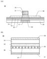
도 1의 (A)는 본 발명의 일 형태에 따른 반도체 장치인, 트랜지스터(10)의 일부의 단면도이다. 또한 도 1의 (B)는 트랜지스터(10)의 영역(50)의 확대도이다.1A is a cross-sectional view of a part of a
도 1의 (A)에 도시된 바와 같이, 트랜지스터(10)는 기판 위에 배치된 도전체(31)와, 도전체(31) 위에 배치된 절연체(32)와, 절연체(32)의 상면에 접하여 배치된 산화물(33)과, 산화물(33)의 상면에 접하여 배치된 절연체(34)와, 절연체(34) 위에 배치된 산화물(46)과, 산화물(46) 위에 배치된 절연체(41)와, 절연체(41) 위에 도전체(31) 및 산화물(46)과 중첩되도록 배치된 도전체(44)를 가진다. 또한 도전체(31)는 절연체(30)에 매립되도록 배치되는 것이 바람직하다.As shown in FIG. 1A, the
도 1의 (A)에서 도전체(31), 절연체(30), 절연체(32), 산화물(33), 절연체(34), 산화물(46), 절연체(41), 및 도전체(44)는 단층 구조로 도시하였지만, 본 실시형태에 나타낸 반도체 장치는 이에 한정되지는 않는다. 도전체(31), 절연체(30), 절연체(32), 산화물(33), 절연체(34), 산화물(46), 절연체(41), 및 도전체(44)는 각각 단층 구조로 하여도 좋고, 2층 이상의 적층 구조로 하여도 좋다.In (A) of FIG. 1, the
산화물(46)은 도전체(44)와 중첩되는 영역에 채널 형성 영역을 가지고, 도전체(44)와 중첩되지 않는 영역에 채널 형성 영역을 협지하도록 소스 영역과 드레인 영역을 가진다. 또한 도 1의 (A)에서 산화물(46) 내의 파선은 소스 영역과 채널 형성 영역의 경계, 및 드레인 영역과 채널 형성 영역의 경계를 나타낸다. 도 1에서는 소스 영역과 채널 형성 영역의 경계, 및 드레인 영역과 채널 형성 영역의 경계가 도전체(44)의 측면과 실질적으로 일치하는 예에 대하여 도시하였다. 다만, 이에 한정되지 않고 소스 영역의 채널 형성 영역 측의 일부 및/또는 드레인 영역의 채널 형성 영역 측의 일부가 도전체(44)와 중첩되는 구성이 되어도 좋다.The
여기서, 트랜지스터(10)에서, 산화물(46)에는 산화물 반도체로서 기능하는 금속 산화물(이하, 산화물 반도체라고도 함)을 사용하는 것이 바람직하다. 예를 들어, 산화물(46)이 되는 금속 산화물로서는, 에너지 갭이 2eV 이상, 바람직하게는 2.5eV 이상인 것을 사용하는 것이 바람직하다. 이와 같이, 에너지 갭이 넓은 금속 산화물을 사용함으로써, 트랜지스터의 오프 전류를 저감할 수 있다.Here, in the
예를 들어, 산화물(46)로서, In-M-Zn 산화물(원소 M은 알루미늄, 갈륨, 이트륨, 구리, 바나듐, 베릴륨, 붕소, 실리콘, 타이타늄, 철, 니켈, 저마늄, 지르코늄, 몰리브데넘, 란타넘, 세륨, 네오디뮴, 하프늄, 탄탈럼, 텅스텐, 또는 마그네슘 등에서 선택된 1종류 또는 복수 종류) 등의 금속 산화물을 사용하는 것이 좋다. 또한 산화물(46)로서 In-Ga 산화물, In-Zn 산화물을 사용하여도 좋다.For example, as
산화물 반도체를 사용한 트랜지스터(10)는 비도통 상태에서 누설 전류(오프 전류)가 매우 작기 때문에, 저소비전력의 반도체 장치를 제공할 수 있다. 또한 산화물 반도체는 스퍼터링법 등을 사용하여 성막될 수 있으므로 고집적형 반도체 장치를 구성하는 트랜지스터에 사용될 수 있다.Since the
한편으로, 산화물 반도체를 사용한 트랜지스터는 산화물 반도체 내의 불순물 및 산소 결손으로 인하여 그 전기 특성이 변동되기 쉽고, 신뢰성이 낮아지는 경우가 있다. 또한 산화물 반도체에 포함되는 수소는 금속 원자와 결합하는 산소와 반응하여 물이 되기 때문에 산소 결손을 형성하는 경우가 있다. 상기 산소 결손에 수소가 들어감으로써 캐리어인 전자가 생성되는 경우가 있다. 따라서, 산소 결손이 포함되어 있는 산화물 반도체를 사용한 트랜지스터는 노멀리 온 특성을 가지기 쉽다. 그러므로, 산화물 반도체 내의 산소 결손은 가능한 한 저감되어 있는 것이 바람직하다.On the other hand, transistors using oxide semiconductors tend to fluctuate in electrical properties due to impurity and oxygen deficiency in the oxide semiconductors, and reliability may be reduced. In addition, hydrogen contained in the oxide semiconductor reacts with oxygen, which is bound to a metal atom, to become water, and thus oxygen deficiency may be formed. When hydrogen enters the oxygen vacancies, electrons as carriers may be generated. Therefore, a transistor using an oxide semiconductor containing oxygen vacancies tends to have normally-on characteristics. Therefore, it is preferable that the oxygen deficiency in the oxide semiconductor is reduced as much as possible.
특히, 산화물(46)에서의 채널 형성 영역과, 게이트 절연막으로서 기능하는 절연체(41)의 계면에 산소 결손이 존재하면, 전기 특성이 변동되기 쉽고, 또한 신뢰성이 낮아지는 경우가 있다.Particularly, when oxygen deficiency exists at the interface between the channel formation region in the
산화물(46)은 2층 이상의 적층 구조로 하여도 좋다. 예를 들어, 산화물(46)은 제 1 산화물층과, 제 1 산화물층 위의 제 2 산화물층과, 제 2 산화물층 위의 제 3 산화물층을 가지는 적층 구조로 하여도 좋다. 제 1 산화물층 위에 제 2 산화물층을 가짐으로써, 제 1 산화물층보다 아래쪽에 형성된 구조물로부터 제 2 산화물층에 대한 불순물의 확산을 억제할 수 있다. 또한 제 3 산화물층 아래에 제 2 산화물층을 가짐으로써, 제 3 산화물층보다 위쪽에 형성된 구조물로부터 제 2 산화물층에 대한 불순물의 확산을 억제할 수 있다.The
또한 산화물(46)의 제 1 산화물층 내지 제 3 산화물층에서, 각 금속 원자의 원자수비가 상이한 구성으로 하는 것이 바람직하다. 구체적으로는, 제 1 산화물층에 사용하는 금속 산화물에서, 금속 원소 중의 원소 M의 원자수비가 제 2 산화물층에 사용하는 금속 산화물에서의 금속 원소 중의 원소 M의 원자수비보다 큰 것이 바람직하다. 또한 제 1 산화물층에 사용하는 금속 산화물에서 In에 대한 원소 M의 원자수비가 제 2 산화물층에 사용하는 금속 산화물에서의 In에 대한 원소 M의 원자수비보다 큰 것이 바람직하다. 또한 제 2 산화물층에 사용하는 금속 산화물에서 원소 M에 대한 In의 원자수비가 제 1 산화물층에 사용하는 금속 산화물에서의 원소 M에 대한 In의 원자수비보다 큰 것이 바람직하다. 또한 제 3 산화물층은 제 1 산화물층 또는 제 2 산화물층에 사용할 수 있는 금속 산화물을 사용할 수 있다.In addition, in the first oxide layer to the third oxide layer of the
또한 제 1 산화물층 및 제 3 산화물층의 전도대 하단의 에너지가 제 2 산화물층의 전도대 하단의 에너지보다 높아지는 것이 바람직하다. 또한 바꿔 말하면 제 1 산화물층 및 제 3 산화물층의 전자 친화력이 제 2 산화물층의 전자 친화력보다 작은 것이 바람직하다.In addition, it is preferable that the energy at the bottom of the conduction band of the first oxide layer and the third oxide layer is higher than the energy at the bottom of the conduction band of the second oxide layer. In other words, it is preferable that the electron affinity of the first oxide layer and the third oxide layer is smaller than the electron affinity of the second oxide layer.
여기서, 제 1 산화물층, 제 2 산화물층, 및 제 3 산화물층에서 전도대 하단의 에너지 준위는 완만하게 변화한다. 바꿔 말하면, 연속적으로 변화 또는 연속 접합한다고도 할 수 있다. 이와 같이 하기 위해서는, 제 1 산화물층과 제 2 산화물층 사이의 계면 및 제 2 산화물층과 제 3 산화물층 사이의 계면에 형성되는 혼합층의 결함 준위 밀도를 낮추는 것이 좋다.Here, in the first oxide layer, the second oxide layer, and the third oxide layer, the energy level at the bottom of the conduction band changes gently. In other words, it can also be said to be continuously changed or continuously joined. To do this, it is desirable to lower the defect level density of the mixed layer formed at the interface between the first oxide layer and the second oxide layer and the interface between the second oxide layer and the third oxide layer.
구체적으로는, 제 1 산화물층과 제 2 산화물층, 제 2 산화물층과 제 3 산화물층이, 산소 이외에 공통된 원소를 가짐으로써(주성분으로 함으로써), 결함 준위 밀도가 낮은 혼합층을 형성할 수 있다. 예를 들어, 제 2 산화물층이 In-Ga-Zn 산화물인 경우, 제 1 산화물층 및 제 3 산화물층으로서, In-Ga-Zn 산화물, Ga-Zn 산화물, 산화 갈륨 등을 사용하면 좋다.Specifically, the first oxide layer and the second oxide layer, the second oxide layer and the third oxide layer have a common element in addition to oxygen (as a main component), so that a mixed layer having a low defect level density can be formed. For example, when the second oxide layer is an In-Ga-Zn oxide, an In-Ga-Zn oxide, Ga-Zn oxide, gallium oxide, or the like may be used as the first oxide layer and the third oxide layer.
이때, 캐리어의 주된 경로는 제 2 산화물층 또는 그 근방, 예를 들어, 제 2 산화물층과 제 3 산화물층의 계면이다. 제 1 산화물층과 제 2 산화물층의 계면, 및 제 2 산화물층과 제 3 산화물층의 계면에서의 결함 준위 밀도를 낮게 할 수 있어, 계면 산란으로 인한 캐리어 전도에 대한 영향이 작고, 높은 온 전류를 얻을 수 있다.At this time, the main path of the carrier is the second oxide layer or its vicinity, for example, the interface between the second oxide layer and the third oxide layer. The defect level density at the interface between the first oxide layer and the second oxide layer and the interface between the second oxide layer and the third oxide layer can be made low, so that the effect on carrier conduction due to interfacial scattering is small and high on current Can get
또한 도전체(44)는 제 1 게이트(톱 게이트라고도 함) 전극으로서 기능하고, 도전체(31)는 제 2 게이트(보텀 게이트라고도 함) 전극으로서 기능한다. 도전체(31)에 인가하는 전위를 도전체(44)에 인가하는 전위와 연동시키지 않고 독립적으로 변화시킴으로써, 트랜지스터(10)의 문턱 전압을 제어할 수 있다. 특히, 도전체(31)에 마이너스의 전위를 인가함으로써, 트랜지스터(10)의 문턱 전압을 0V보다 크게 하고, 도전체(44)에 인가하는 전압이 0V일 때의 드레인 전류(이하, Icut이라고 하는 경우가 있음)를 작게 할 수 있다.Further, the
트랜지스터(10)에서, 보텀 게이트에 전압(Vbg[V])이 인가된 상태에서, 톱 게이트에 전압(Vth[V])보다 큰 전압이 인가되면, 산화물(46)에 채널이 형성되기 시작한다. 이때의 전압(Vth)을 트랜지스터(10)의 문턱 전압이라고 할 수 있다.In the
도 1의 (A)에 도시된 트랜지스터(10)는 도전체(31)에 전압(Vbg)을 인가함으로써, 전압(Vth)을 크게 하고, 트랜지스터(10)의 Icut을 작게 할 수 있다. 바꿔 말하면, 트랜지스터(10)에 노멀리 오프의 전기 특성을 부여할 수 있다.The
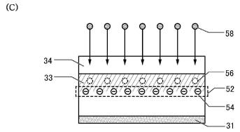
또한 트랜지스터(10)는 도 1의 (B)에 도시된 바와 같이, 절연체(32)와 산화물(33) 사이에서 고정 전하(54)가 유지된다. 자세한 사항은 후술하지만, 트랜지스터(10)는 고정 전하(54)에 의하여 전압(Vth)을 크게 하고, 트랜지스터(10)의 Icut을 작게 할 수 있다.Also, as shown in FIG. 1B, the
또한 도 1의 (B)에 도시된 바와 같이, 절연체(32)와 산화물(33) 사이에는 혼합층(52)이 형성되는 것이 바람직하고, 혼합층(52)이 고정 전하(54)를 가지는 것이 바람직하다. 여기서, 고정 전하(54)는 절연체(32) 위에 산화물(33)을 성막하였을 때, 절연체(32)와 산화물(33) 사이에 형성되는 혼합층(52)에 전자가 포획됨으로써 형성된다. 또한 혼합층(52)은 절연체(32)에 포함되는 원자 중 적어도 하나와, 산화물(33)에 포함되는 원자 중 적어도 하나를 포함하는 것이다.In addition, as shown in FIG. 1B, it is preferable that a
절연체(32)는 산화물(33)을 스퍼터링법 등으로 성막하였을 때, 믹싱(mixing)이 발생할 정도로 부드러운 것이 바람직하다. 예를 들어, 절연체(32)로서, 산화 실리콘, 산화 질화 실리콘, 질화 산화 실리콘, 질화 실리콘, 플루오린을 첨가한 산화 실리콘, 탄소를 첨가한 산화 실리콘, 탄소 및 질소를 첨가한 산화 실리콘, 구멍(hole)을 가지는 산화 실리콘 등을 사용하는 것이 바람직하다.The
산화물(33)은 상기 원소 M, 특히 갈륨 등 산소와의 결합력이 강한 금속 원소를 포함하는 금속 산화물을 사용하는 것이 바람직하다. 예를 들어, 산화물(33)에 산화 갈륨을 사용하면 좋다. 여기서, 산화물(33)은 많은 갈륨 원자를 포함하는 것이 바람직하고, 예를 들어 산화물(46)에 포함되는 금속 원소에서의 갈륨의 원자수비보다 산화물(33)에 포함되는 금속 원소에서의 갈륨의 원자수비를 크게 하면 좋다.It is preferable that the
또한 산화물(33)로서 산화물(46)과 마찬가지로, 인듐 및 갈륨을 포함하는 산화물, 또는 인듐, 갈륨, 및 아연을 포함하는 산화물 등을 사용하여도 좋다. 이 경우, 예를 들어, 산화물(46)에 포함되는 금속 원소에서의 인듐의 원자수비보다 산화물(33)에 포함되는 금속 원소에서의 인듐의 원자수비를 작게 하면 좋다.In addition, as the
산화물(33) 내의 산소 결손에 수소가 보전되어, 양전하를 가지는 도너 불순물이 형성되는 경우가 있다. 그러나 갈륨 등 산소와의 결합력이 강한 금속 원소를 포함하는 금속 산화물을, 산화물(33)에 사용함으로써 산화물(33)에 산소가 결합되기 쉽게 하고, 산소 결손을 저감시킬 수 있다. 이에 의하여, 양전하를 가지는 도너 불순물을 저감시킬 수 있다. 따라서, 절연체(32)와 산화물(33) 사이에서 마이너스의 고정 전하(54)가 현재화된다.Hydrogen is preserved in the oxygen deficiency in the
산화물(33) 위에 제공되는 절연체(34)로서는, 산소를 포함하는 절연체를 사용하는 것이 바람직하다. 특히, 절연체(34)는 화학량론적 조성을 만족시키는 산소보다 많은 산소(이하, 과잉 산소라고도 함)를 포함하는 것이 바람직하다. 즉, 절연체(34)로부터 산소가 산화물(33)로 확산됨으로써, 산화물(33) 내의 산소 결손을 저감시킬 수 있다. 또한 절연체(32)도 절연체(34)와 마찬가지로 산소를 포함하는 절연체를 사용하는 것이 바람직하다.As the
예를 들어, 절연체(34)에 사용할 수 있는 과잉 산소를 포함하는 절연체로서, 가열에 의하여 일부의 산소가 이탈되는 산화물 재료를 사용하는 것이 바람직하다. 가열에 의하여 산소가 이탈되는 산화물이란, TDS(Thermal Desorption Spectroscopy) 분석에서 단위 막 두께당 산소 원자로 환산한 산소의 이탈량이 1.0×10¹⁸atoms/cm3 이상, 바람직하게는 1.0×10¹⁹atoms/cm3 이상, 더 바람직하게는 2.0×10¹⁹atoms/cm3 이상, 더욱 바람직하게는 3.0×10²⁰atoms/cm3 이상인 산화물막이다. 또한 상기 TDS 분석 시의 막의 표면 온도로서는 100℃이상 700℃ 이하의 범위가 바람직하다.For example, as an insulator containing excess oxygen that can be used for the
예를 들어, 절연체(34)로서 과잉 산소를 가지는 산화 실리콘, 산화 질화 실리콘, 질화 산화 실리콘, 질화 실리콘, 플루오린을 첨가한 산화 실리콘, 탄소를 첨가한 산화 실리콘, 탄소 및 질소를 첨가한 산화 실리콘, 구멍을 가지는 산화 실리콘을 사용할 수 있다. 특히, 산화 실리콘 및 산화 질화 실리콘은 열에 대하여 안정적이기 때문에 바람직하다.For example, as the
이와 같은 절연체(34)를 제공함으로써 절연체(34) 위의 산화물(46)에 산소를 공급할 수도 있다. 또한 절연체(41)로서 마찬가지의 과잉 산소를 포함하는 절연체를 사용함으로써 산화물(46)의 채널 형성 영역에 산소를 공급하고, 산소 결손을 저감시킬 수 있다.By providing such an
다음으로 도 2를 사용하여, 고정 전하(54)에 의한, 도 1에 도시된 트랜지스터(10)의 문턱 전압의 변화량(ΔVth)에 대하여 설명한다. 여기서, 도 2의 (A)는 트랜지스터(10)의 톱 게이트와 보텀 게이트 사이의 모델을 도시한 모식도이고, 도 2의 (B)는 도 2의 (A)에 도시된 모델에 대응하는 등가 회로도이다.Next, the amount of change ΔV th of the threshold voltage of the
도 2의 (A)에 도시된 트랜지스터(10)의 모델에서, 도전체(31)는 보텀 게이트로서의 기능을 가지고, 절연체(32), 산화물(33), 및 절연체(34)는 보텀 게이트의 게이트 절연체로서의 기능을 가지고, 산화물(46)은 채널 형성 영역으로서의 기능을 가지고, 도전체(44)는 톱 게이트로서의 기능을 가지고, 절연체(41)는 톱 게이트의 게이트 절연체로서의 기능을 가진다. 또한 절연체(32)와 산화물(33) 사이에 고정 전하(54)가 유지되고, 고정 전하(54)의 전하량을 Qb로 한다.In the model of the
도 2의 (A)에 도시된 트랜지스터(10)의 모델에서 도전체(31)에 전압(Vbg)이 인가된 상태로, 도전체(44)에 전압(Vth)을 인가하면, 산화물(46) 내에 채널이 형성되기 시작된다. 이하에서는 트랜지스터(10)에서, 채널이 형성되는 영역을 영역(P)으로 한다. 예를 들어, 산화물(46)이 상술한 제 1 산화물층 내지 제 3 산화물층의 적층 구조인 경우, 제 2 산화물층과 제 3 산화물층의 계면 근방에 영역(P)이 형성되는 경우가 있다.When the voltage V th is applied to the
또한 도 2의 (A)에서, 채널이 산화물(46) 내에 형성되는 것으로 하였지만, 이에 한정되지 않는다. 예를 들어, 산화물(46)의 절연체(41) 측의 계면 근방에 채널이 형성되는 경우도 있다.Further, in Fig. 2A, the channel is assumed to be formed in the
여기서, 절연체(32)의 정전 용량을 Cb로 하고, 산화물(33)과 절연체(34)와 산화물(46)의 영역(P)보다 아래의 부분의 직렬 합성 용량을 Cm으로 하고, 절연체(41)와 산화물(46)의 영역(P)보다 위의 부분의 직렬 합성 용량을 Ct로 하면, 트랜지스터(10)의 모델은 도 2의 (B)에 도시된 등가 회로도에서 나타내어진다.Here, the electrostatic capacity of the
도 2의 (B)에 도시된 모델에서 고정 전하(54)에 의한, 트랜지스터(10)의 문턱 전압의 변화량(ΔVth)을 구하면 다음 수학식으로 나타낼 수 있다.In the model shown in FIG. 2B, when the change amount ΔV th of the threshold voltage of the
[수학식 1][Equation 1]

상기 식에 따르면, ΔVth는 고정 전하(54)의 전하량(Qb)에 비례한다. 즉, 절연체(32)와 산화물(33) 사이에 유지되는, 마이너스의 고정 전하(54)의 전하량(Qb)(Qb는 마이너스의 값을 취함)이 작을수록 트랜지스터(10)의 전압(Vth)을 크게 하고, Icut을 충분히 작게 할 수 있다. 예를 들어, 혼합층(52)이 -2.0×10¹²e/cm2 이하의 고정 전하(54)를 가지는 것이 바람직하다. 여기서, e는 전기 소량을 나타낸다.According to the above formula, ΔV th is proportional to the amount of charge Q b of the fixed
이와 같이, 절연체(32)와 산화물(33) 사이에 유지되는, 마이너스의 고정 전하(54)에 의하여, 트랜지스터(10)에서는 문턱 전압(Vth)을 플러스 측으로 시프트시킬 수 있다. 이에 의하여, 절댓값이 작은 마이너스의 전압(VBG)을 도전체(31)에 인가함으로써, 문턱 전압(Vth)을 플러스 측으로 시프트하고, 트랜지스터(10)의 Icut을 충분히 작게 할 수 있다. 따라서, 절댓값이 작은 마이너스의 전압(VBG)으로 동작하고, 노멀리 오프의 전기 특성을 가지는 트랜지스터(10)를 제공할 수 있다.In this way, the threshold voltage V th can be shifted to the positive side in the
또한 상기 식에서 나타낸 바와 같이, Cb와 Cm의 비, 즉 Cb/Cm의 값이 작을수록 ΔVth가 크게 된다. 따라서, 예를 들어 절연체(32)의 정전 용량을, 산화물(33)과 절연체(34)와 산화물(46)의 영역(P)보다 아래의 부분의 직렬 합성 용량보다 작게 하면 좋다. 구체적으로는, 예를 들어, 절연체(32)로서 비유전율이 낮은 실리콘계의 절연막을 사용하거나, 또는 절연체(32)의 막 두께를 절연체(34)보다 크게 하면 좋다.In addition, as shown in the above formula, the smaller the value of C b and C m , that is, C b / C m, the greater ΔV th . Therefore, for example, the capacitance of the
또한 도 1의 (A) 등에서는 트랜지스터(10)로서, 제 2 게이트 전극으로서 기능하는 도전체(31)를 제공하는 구성에 대하여 도시하였지만, 본 실시형태에 나타내는 반도체 장치는 이에 한정되지 않는다. 예를 들어, 고정 전하(54)가 충분히 많이 유지되어 있는 경우, 제 2 게이트 전극으로서 기능하는 도전체(31)를 제공하여 마이너스의 전압(VBG)을 인가하지 않아도 트랜지스터(10)의 문턱 전압(Vth)을 플러스 측으로 시프트하고, Icut을 충분히 작게 할 수 있는 경우가 있다. 따라서, 이 경우 도 2의 (C)에 도시된 트랜지스터(10a)와 같이, 도전체(31)를 제공하지 않는 구성으로 하여도 좋다.1 (A) and the like, the configuration of providing the
또한 도 1의 (A) 등에서는 트랜지스터(10)로서 산화물(46) 위에 제공된 도전체(44)에서 트랜지스터(10)의 스위칭을 제어하고, 산화물(46) 아래에 제공된 도전체(31)에서 트랜지스터(10)의 문턱 전압을 제어하는 구성에 대하여 도시하였지만, 본 실시형태에 나타내는 반도체 장치는 이에 한정되지 않는다. 예를 들어, 도 2의 (D)에 도시된 트랜지스터(10b)와 같이, 산화물(46) 아래에 트랜지스터(10)의 스위칭을 제어하는 도전체(44)를 제공하고, 산화물(46) 위에 트랜지스터(10)의 문턱 전압을 제어하는 도전체(31)를 제공하는 구성으로 하여도 좋다. 여기서, 도전체(44)는 절연체(40) 위에 제공되는 것으로 한다.In addition, in (A) of FIG. 1, the switching of the
도전체(44)와 산화물(46) 사이에는 절연체(41)가 제공되고, 도전체(31)와 산화물(46) 사이에는 절연체(32), 산화물(33), 및 절연체(34)가 제공된다. 트랜지스터(10)와 마찬가지로, 절연체(32)와 산화물(33) 사이에는 고정 전하가 유지되어 있다. 또한 절연체(32)와 산화물(33) 사이에는, 이들의 혼합층이 형성되고, 상기 혼합층이 마이너스의 고정 전하를 가지는 것이 바람직하다. 또한 도전체(44), 절연체(41), 산화물(46), 절연체(32), 산화물(33), 절연체(34), 및 도전체(31)는 트랜지스터(10)와 마찬가지의 재료를 사용할 수 있다.An
또한 도 2의 (D)에 도시된 바와 같이 산화물(46)에 접하여, 트랜지스터(10)의 소스 전극 또는 드레인 전극으로서 기능하는 도전체(48a)와 도전체(48b)를 제공하는 구성으로 하여도 좋다.In addition, as shown in FIG. 2D, even if the structure is provided in contact with the
다음으로 도 3을 사용하여, 절연체(32)와 산화물(33) 사이에 고정 전하(54)가 형성되는 모델의 일례에 대하여 설명한다. 여기서, 도 3의 (A) 내지 (D)는 도 1의 (B)에 대응한 것이다.Next, an example of a model in which a fixed
우선, 기판(도시 생략) 위에 도전체(31)를 형성하고, 도전체(31) 위에 절연체(32)를 형성한다. 여기서, 절연체(32)는 후술하는 산화물(33)의 스퍼터링 성막에서 믹싱이 발생할 정도로 부드러운 막인 것이 바람직하다. 따라서, 절연체(32)는 예를 들어 화학 기상 성장(CVD:Chemical Vapor Deposition)법 등을 사용하여 성막하는 것이 바람직하다.First, a
다음으로 절연체(32)의 상면에 접하여 스퍼터링법을 사용하여 산화물(33)을 형성한다(도 3의 (A) 참조). 여기서, 스퍼터링법을 사용하여 산화물(33)을 성막함으로써, 절연체(32)의 표면에서 믹싱이 발생하고, 절연체(32)와 산화물(33) 사이에 혼합층(52)이 형성된다.Next, the
또한 산화물(33)의 스퍼터링 성막에서는 갈륨을 포함하는 타깃을 사용하면 좋다. 또한 인듐 및 갈륨을 포함하는 타깃, 또는 인듐, 갈륨, 및 아연을 포함하는 타깃을 사용하여도 좋다.In addition, in the sputtering film formation of the
다음으로 산화물(33) 위에 절연체(34)를 형성한다(도 3의 (B) 참조). 예를 들어, CVD법 등을 사용하여 절연체(34)를 성막할 수 있다. 여기서, CVD법 등의 성막 대미지에 의하여, 산화물(33)에 산소 결손(56)이 형성된다. 또한 성막 분위기에 포함되는 수소가 산화물(33)에 혼입되고, 산소 결손(56)에 상기 수소가 보전된다. 이에 의하여, 상기 수소는 양전하를 가지는 도너 불순물이 되고, n형의 캐리어를 생성한다. 상기 캐리어 등의 전하가 전자 트랩층으로서 기능하는 혼합층(52)에 포획됨으로써, 마이너스의 고정 전하(54)가 형성된다.Next, an
다음으로 절연체(34)에 산소(58)를 첨가한다(도 3의 (C) 참조). 산소(58)는 예를 들어 절연체(34) 위에, 산소(58)를 포함하는 분위기에서 스퍼터링 성막을 수행함으로써 첨가되어도 좋다. 또한 예를 들어 이온 주입법, 이온 도핑법, 플라스마 이머전 이온 주입법 등을 사용하여도 좋다. 또한 예를 들어 산소를 포함하는 분위기에서 절연체(34)의 성막을 수행함으로써 첨가되어도 좋다. 여기서, 산소(58)는 예를 들어 산소 라디칼로서 절연체(34)에 첨가되지만, 산소(58)가 첨가될 때의 상태는 이에 한정되지 않는다. 산소(58)는 산소 원자, 또는 산소 이온 등의 상태로 절연체(34)에 첨가되어도 좋다.Next,
다음으로 절연체(34) 위에 스퍼터링법을 사용하여 산화물(46)을 형성한다(도 3의 (D) 참조). 여기서, 산화물(46)의 스퍼터링법에 의한 성막을 산소를 포함하는 분위기에서 수행함으로써 도 3의 (C)에 도시된 산소(58)의 첨가를 수행하지 않아도, 절연체(34)에 산소를 첨가할 수 있다.Next, an
또한, 산화물(46) 성막 후에 가열 처리를 수행하는 것이 바람직하다. 가열 처리는 250℃ 이상 650℃ 이하, 바람직하게는 300℃ 이상 500℃ 이하, 더 바람직하게는 320℃ 이상 450℃ 이하에서 수행하면 좋다. 이에 의하여, 첨가된 산소(58)를 산화물(33)로 확산시켜, 산화물(33) 내의 산소 결손(56)을 보전할 수 있다(도 3의 (D) 참조). 이로써, 산화물(33) 내의 양전하를 가지는 도너 불순물을 저감시킬 수 있다. 따라서, 트랜지스터(10)에서 절연체(32)와 산화물(33) 사이에서 고정 전하(54)가 현재화된다.In addition, it is preferable to perform a heat treatment after the
그리고, 산화물(46) 위에 절연체(41)를 형성하고, 절연체(41) 위에 도전체(44)를 형성한다. 이로써 트랜지스터(10)를 제작할 수 있다.Then, an
상술한 바와 같이, 본 발명의 일 형태에 의하여 문턱 전압이 큰 반도체 장치를 제공할 수 있다. 또는, 본 발명의 일 형태에 의하여 노멀리 오프의 전기 특성을 가지는 반도체 장치를 제공할 수 있다. 또는 본 발명의 일 형태에 의하여 절댓값이 작은 전압으로 동작하는 반도체 장치를 제공할 수 있다. 또는, 본 발명의 일 형태에 의하여 양호한 전기 특성을 가지는 반도체 장치를 제공할 수 있다.As described above, according to one embodiment of the present invention, a semiconductor device having a large threshold voltage can be provided. Alternatively, according to one embodiment of the present invention, a semiconductor device having normally-off electrical characteristics can be provided. Alternatively, according to one embodiment of the present invention, a semiconductor device operating with a voltage having a small absolute value can be provided. Alternatively, according to one embodiment of the present invention, a semiconductor device having good electrical characteristics can be provided.
이상, 본 실시형태에 나타내어진 구성, 구조, 방법 등은 다른 실시형태에 나타내어지는 구성, 구조, 방법 등과 적절히 조합하여 사용할 수 있다.As described above, the structures, structures, methods, and the like shown in this embodiment can be used in appropriate combinations of structures, structures, methods, and the like shown in other embodiments.
(실시형태 2)(Embodiment 2)
여기서는 상술한 실시형태에 나타내어진 트랜지스터의 구체적인 구성의 일례에 대하여 도 4 내지 도 9를 사용하여 설명한다.Here, an example of a specific configuration of the transistor shown in the above-described embodiment will be described with reference to Figs.
<반도체 장치의 구성예><Structure example of semiconductor device>
도 4의 (A)는 본 발명의 일 형태에 따른 트랜지스터(400a)의 상면도이다. 또한 도 4의 (B)는 도 4의 (A)에서 일점쇄선 A1-A2로 나타낸 부분의 단면도이다. 즉, 트랜지스터(400a)의 채널 길이 방향의 단면도를 도시하였다. 도 4의 (C)는 도 4의 (A)에서 일점쇄선 A3-A4로 나타낸 부분의 단면도이다. 즉, 트랜지스터(400a)의 채널 폭 방향의 단면도를 도시하였다. 도 4의 (A)의 상면도에서는 도면의 명료화를 위하여 요소의 일부를 생략하여 도시되었다. 또한 트랜지스터의 채널 길이 방향이란, 기판과 수평의 면 내에서 소스(소스 영역 또는 소스 전극) 및 드레인(드레인 영역 또는 드레인 전극) 간에 있어서, 캐리어가 이동하는 방향을 의미하고, 채널 폭 방향은 기판과 수평의 면 내에서, 채널 길이 방향에 대하여 수직인 방향을 의미한다.4A is a top view of the
도 4의 (A), (B), (C)에 도시된 바와 같이, 트랜지스터(400a)는 도전체(310)와, 도전체(310) 위에 배치된 절연체(302), 산화물(303), 및 절연체(402)와, 절연체(302), 산화물(303), 및 절연체(402) 위에 배치된 산화물(406a)과, 산화물(406a) 위에 배치된 산화물(406b)과, 산화물(406b) 위에 이격되어 배치된 도전체(416a) 및 도전체(416b)와, 산화물(406b), 도전체(416a), 및 도전체(416b) 위에 배치된 산화물(406c)과, 산화물(406c) 위에 배치된 절연체(412)와, 적어도 일부가 산화물(406b)과 중첩되도록 절연체(412) 위에 배치된 도전체(404)를 가진다.As shown in (A), (B), (C) of FIG. 4, the
여기서, 도전체(310)는 상술한 실시형태에 나타내어진 트랜지스터(10)의 도전체(31)에 대응한다. 또한 절연체(302)는 상술한 실시형태에 나타내어진 트랜지스터(10)의 절연체(32)에 대응한다. 또한 산화물(303)은 상술한 실시형태에 나타내어진 트랜지스터(10)의 산화물(33)에 대응한다. 또한 절연체(402)는 상술한 실시형태에 나타내어진 트랜지스터(10)의 절연체(34)에 대응한다. 또한 산화물(406a), 산화물(406b), 및 산화물(406c)(이하, 통틀어 산화물(406)이라고 하는 경우가 있음)은 상술한 실시형태에 나타내어진 트랜지스터(10)의 산화물(46)에 대응한다. 또한, 절연체(412)는 상술한 실시형태에 나타내어진 트랜지스터(10)의 절연체(41)에 대응한다. 또한 도전체(404)는 상술한 실시형태에 나타내어진 트랜지스터(10)의 도전체(44)에 대응한다.Here, the
상기 실시형태와 마찬가지로, 트랜지스터(400a)에서도 절연체(302)와 산화물(303) 사이에는, 마이너스의 고정 전하가 유지된다. 마이너스의 고정 전하에 의하여 트랜지스터(400a)에서는 문턱 전압(Vth)을 플러스 측으로 시프트시킬 수 있기 때문에 절댓값이 작은 마이너스의 전압으로, 문턱 전압(Vth)을 크게 하고, 트랜지스터(400a)의 Icut을 충분히 작게 할 수 있다. 따라서, 절댓값이 작은 전압으로 동작하고, 노멀리 오프의 전기 특성을 가지는 트랜지스터(400a)를 제공할 수 있다.Similarly to the above-described embodiment, in the
또한 절연체(402), 산화물(406a), 산화물(406b), 산화물(406c), 도전체(416a), 도전체(416b), 절연체(412), 및 도전체(404) 등 위에 절연체(410)가 배치된다. 또한 절연체(410) 위에 절연체(420)가 배치되고, 절연체(420) 위에 절연체(422)가 배치되는 구성으로 하여도 좋다. 또한 절연체(422), 절연체(420), 절연체(410), 배리어막(417a), 및 배리어막(417b)에 형성된 개구에 도전체(438a) 및 도전체(438b)가 형성된다.Also,
도전체(310)는 절연체(301)에 형성된 개구에 제공된다. 절연체(301)의 개구의 내벽에 접하여 제 1 도전체층이 형성되고, 그 내측에 제 2 도전체층이 형성된다. 여기서, 제 1 도전체층 및 제 2 도전체층의 상면의 높이와 절연체(301)의 상면의 높이는 같은 정도로 할 수 있다. 도전체(310)는 게이트 전극의 한쪽으로서 기능할 수 있다.The
여기서, 제 1 도전체층은, 물 또는 수소 등의 불순물이 투과하기 어려운 도전성 재료를 사용하는 것이 바람직하다. 또한 예를 들어, 탄탈럼, 질화 탄탈럼, 루테늄 또는 산화 루테늄 등을 사용하는 것이 바람직하고, 단층 또는 적층으로 하면 좋다. 이에 의하여, 절연체(401)보다 아래층으로부터 수소, 물 등의 불순물이 도전체(310)를 통하여 위층으로 확산되는 것을 억제할 수 있다. 또한 제 1 도전체층은 수소 원자, 수소 분자, 물 분자, 질소 원자, 질소 분자, 산화 질소 분자(N2O, NO, NO2 등), 또는 구리 원자 등의 불순물 중 적어도 하나가 투과하기 어려운 것이 바람직하다. 또한, 제 1 도전체층은 산소 원자 또는 산소 분자가 투과하기 어려운 것이 바람직하다. 또한 이하에서 불순물이 투과하기 어려운 도전성 재료에 대하여 기재하는 경우도 마찬가지이다. 제 1 도전체층이 산소의 투과를 억제하는 기능을 가짐으로써, 제 2 도전체층의 도전율이 산화로 인하여 저하되는 것을 방지할 수 있다.Here, it is preferable to use a conductive material in which impurities such as water or hydrogen are difficult to permeate as the first conductor layer. Moreover, it is preferable to use, for example, tantalum, tantalum nitride, ruthenium or ruthenium oxide, and may be a single layer or a lamination. Accordingly, impurities such as hydrogen and water from the lower layer than the
절연체(302), 산화물(303), 및 절연체(402)는 게이트 절연막으로서 기능할 수 있다. 절연체(302)는 절연체(32)의 기재, 산화물(303)은 산화물(33)의 기재, 절연체(402)는 절연체(34)의 기재를 참작할 수 있다.The
다음으로 산화물(406a), 산화물(406b), 및 산화물(406c)에 사용할 수 있는, 산화물 반도체로서 기능하는 금속 산화물(이하, 산화물 반도체라고도 함)에 대하여 설명한다. 또한 본 명세서 등에서 질소를 가지는 금속 산화물도 금속 산화물(metal oxide)이라고 총칭하는 경우가 있다. 또한 질소를 가지는 금속 산화물을 금속 산질화물(metal oxynitride)이라고 불러도 좋다.Next, a metal oxide (hereinafter also referred to as an oxide semiconductor) that functions as an oxide semiconductor that can be used for the
산화물(406a), 산화물(406b), 및 산화물(406c)로서 사용하는 금속 산화물은, 적어도 인듐을 포함하는 것이 바람직하다. 특히 인듐 및 아연을 포함하는 것이 바람직하다. 또한 이들에 더하여 원소 M(M은 갈륨, 알루미늄, 실리콘, 붕소, 이트륨, 구리, 바나듐, 베릴륨, 타이타늄, 철, 니켈, 저마늄, 지르코늄, 몰리브데넘, 란타넘, 세륨, 네오디뮴, 하프늄, 탄탈럼, 텅스텐, 또는 마그네슘 등으로부터 선택된 일종 또는 복수 종류)이 포함되는 것이 바람직하다.It is preferable that the metal oxide used as
또한 상기 금속 산화물은 에너지 갭이 2eV 이상, 바람직하게는 2.5eV 이상이다. 이와 같이, 에너지 갭이 넓은 금속 산화물을 사용함으로써, 트랜지스터의 오프 전류를 저감시킬 수 있다.Further, the metal oxide has an energy gap of 2 eV or more, preferably 2.5 eV or more. As described above, by using a metal oxide having a wide energy gap, the off-state current of the transistor can be reduced.
또한 금속 산화물로서 In-M-Zn 산화물을 사용하는 경우, 스퍼터링 타깃으로서는 다결정 In-M-Zn 산화물을 포함하는 타깃을 사용하는 것이 바람직하다. 또한 성막되는 금속 산화물의 원자수비는 상기 스퍼터링 타깃에 포함되는 금속 원소의 원자수비의 ±40%의 변동을 포함한다. 예를 들어, 금속 산화물의 성막에 사용하는 스퍼터링 타깃의 조성이 In:Ga:Zn=4:2:4.1[원자수비]인 경우, 성막되는 금속 산화물의 조성은 In:Ga:Zn=4:2:3[원자수비] 근방이 되는 경우가 있다. 또한 금속 산화물에 사용하는 스퍼터링 타깃의 조성이 In:Ga:Zn=5:1:7[원자수비]인 경우, 성막되는 금속 산화물의 조성은 In:Ga:Zn=5:1:6[원자수비]의 근방이 되는 경우가 있다.Moreover, when using In-M-Zn oxide as a metal oxide, it is preferable to use a target containing a polycrystalline In-M-Zn oxide as a sputtering target. In addition, the atomic ratio of the metal oxide to be formed includes a variation of ± 40% of the atomic ratio of the metal elements included in the sputtering target. For example, when the composition of the sputtering target used to form the metal oxide is In: Ga: Zn = 4: 2: 4.1 [atomic ratio], the composition of the metal oxide to be formed is In: Ga: Zn = 4: 2 : 3 [atomic defense] It may be near. In addition, when the composition of the sputtering target used for the metal oxide is In: Ga: Zn = 5: 1: 7 [atomic ratio], the composition of the metal oxide to be formed is In: Ga: Zn = 5: 1: 6 [atomic ratio ].
또한 금속 산화물이 가지는 성질은 원자수비에 의하여 일의적으로 정해지지 않는다. 같은 원자수비이어도 형성 조건에 따라 금속 산화물의 성질이 상이한 경우가 있다. 예를 들어, 금속 산화물을 스퍼터링 장치로 성막하는 경우, 타깃의 원자수비로부터 벗어난 원자수비를 가지는 막이 형성된다. 또한 성막 시의 기판 온도에 따라서는, 타깃의 [Zn]보다, 막의 [Zn]이 작아지는 경우가 있다. 따라서, 도시된 영역은 금속 산화물이 특정한 특성을 가지는 경향이 있는 원자수비를 나타내는 영역이고, 영역 A 내지 영역 C의 경계는 엄밀하지 않다.In addition, the properties of the metal oxide are not uniquely determined by the atomic ratio. Even in the same atomic ratio, the properties of the metal oxide may be different depending on the formation conditions. For example, when a metal oxide is formed by a sputtering device, a film having an atomic ratio deviating from the atomic ratio of the target is formed. Further, depending on the substrate temperature at the time of film formation, [Zn] of the film may be smaller than that of the target [Zn]. Therefore, the illustrated regions are regions showing atomic ratios in which metal oxides tend to have specific characteristics, and the boundaries between regions A to C are not rigid.
또한 트랜지스터에는 캐리어 밀도가 낮은 금속 산화물을 사용하는 것이 바람직하다. 금속 산화물의 캐리어 밀도를 낮추기 위해서는 금속 산화물 중의 불순물 농도를 낮게 하여 결함 준위 밀도를 낮게 하면 좋다. 본 명세서 등에서, 불순물 농도가 낮고 결함 준위 밀도가 낮은 것을 고순도 진성 또는 실질적으로 고순도 진성이라고 한다. 예를 들어, 산화물(406b)에서의 캐리어 밀도를 8×10¹¹/cm3 미만, 바람직하게는 1×10¹¹/cm3 미만, 더 바람직하게는 1×10¹⁰/cm3 미만이며 1×10⁻⁹/cm3 이상으로 하면 좋다. 고순도 진성 또는 실질적으로 고순도 진성인 금속 산화물은 캐리어 발생원이 적기 때문에, 캐리어 밀도를 낮게 할 수 있다.In addition, it is preferable to use a metal oxide having a low carrier density for the transistor. In order to lower the carrier density of the metal oxide, the concentration of impurities in the metal oxide may be lowered to lower the density of defect states. In this specification and the like, a low-purity intrinsic or a substantially high-purity intrinsic having a low impurity concentration and a low defect level density. For example, the carrier density in
또한 고순도 진성 또는 실질적으로 고순도 진성인 금속 산화물은 결함 준위 밀도가 낮기 때문에, 트랩 준위 밀도도 낮아지는 경우가 있다.In addition, since the high purity intrinsic or substantially high purity intrinsic metal oxide has a low defect level density, the trap level density may also be lowered.
또한 금속 산화물의 트랩 준위에 포획된 전하는 소실하는 데 걸리는 시간이 길어, 마치 고정 전하처럼 작용하는 경우가 있다. 그래서 트랩 준위 밀도가 높은 금속 산화물에 채널 형성 영역이 형성되는 트랜지스터는 전기 특성이 불안정한 경우가 있다.In addition, the charges trapped at the trap level of the metal oxide take a long time to disappear, so it may act as a fixed charge. Therefore, a transistor in which a channel formation region is formed in a metal oxide having a high trap level density may have unstable electrical properties.
따라서, 트랜지스터의 전기 특성을 안정시키기 위하여 금속 산화물 내의 불순물 농도를 저감시키는 것이 유효하다. 또한 금속 산화물 내의 불순물 농도를 저감시키기 위해서는, 근접한 막 내의 불순물 농도도 저감시키는 것이 바람직하다. 불순물로서는, 수소, 알칼리 금속, 알칼리 토금속, 실리콘 등이 있다.Therefore, it is effective to reduce the concentration of impurities in the metal oxide in order to stabilize the electrical properties of the transistor. Moreover, in order to reduce the impurity concentration in the metal oxide, it is preferable to also reduce the impurity concentration in the adjacent film. Examples of impurities include hydrogen, alkali metal, alkaline earth metal, and silicon.
여기서 금속 산화물 내에서 각 불순물이 미치는 영향에 대하여 설명한다.Here, the effect of each impurity in the metal oxide will be described.
금속 산화물에서 14족 원소 중 하나인 실리콘이나 탄소가 포함되면, 금속 산화물에서 결함 준위가 형성된다. 그래서 금속 산화물에서의 실리콘이나 탄소의 농도와, 금속 산화물과의 계면 근방의 실리콘이나 탄소 이차 이온 질량 분석법(SIMS: Secondary Ion Mass Spectrometry)에 의하여 얻어지는 농도를 2×10¹⁸atoms/cm3 이하, 바람직하게는 2×10¹⁷atoms/cm3 이하로 한다.When silicon or carbon, which is one of Group 14 elements in the metal oxide, is included, a defect level is formed in the metal oxide. Therefore, the concentration obtained by silicon or carbon in the metal oxide and the silicon or carbon secondary ion mass spectrometry (SIMS) near the interface with the metal oxide is preferably 2 × 10 18 atoms / cm 3 or less. It should be 2 x 10 17 atoms / cm 3 or less.
또한 금속 산화물에 알칼리 금속 또는 알칼리 토금속이 포함되면, 결함 준위를 형성하고, 캐리어를 생성하는 경우가 있다. 따라서, 알칼리 금속 또는 알칼리 토금속이 포함되는 금속 산화물을 사용한 트랜지스터는 노멀리 온 특성을 가지기 쉽다. 그래서 금속 산화물 내의 알칼리 금속 또는 알칼리 토금속의 농도를 저감시키는 것이 바람직하다. 구체적으로는 SIMS에 의하여 얻어지는 금속 산화물 내의 알칼리 금속 또는 알칼리 토금속의 농도를 1×10¹⁸atoms/cm3 이하, 바람직하게는 2×10¹⁶atoms/cm3 이하로 한다.Moreover, when an alkali metal or alkaline earth metal is contained in a metal oxide, a defect level may be formed and a carrier may be produced. Therefore, a transistor using a metal oxide containing an alkali metal or alkaline earth metal is likely to have normally-on characteristics. Therefore, it is desirable to reduce the concentration of the alkali metal or alkaline earth metal in the metal oxide. Specifically, the concentration of the alkali metal or alkaline earth metal in the metal oxide obtained by SIMS is 1 × 10 18 atoms / cm 3 or less, preferably 2 × 10 16 atoms / cm 3 or less.
또한 금속 산화물막에 포함되는 수소는 금속 원자와 결합하는 산소와 반응하여 물이 되기 때문에 산소 결손(Vo)을 형성하는 경우가 있다. 상기 산소 결손(Vo)에 수소가 들어감으로써 캐리어인 전자가 생성되는 경우가 있다. 또한 수소의 일부가 금속 원자와 결합하는 산소와 결합하여 캐리어인 전자를 생성하는 경우가 있다. 따라서, 수소가 포함된 금속 산화물을 사용한 트랜지스터는 노멀리 온 특성을 가지기 쉽다. 그러므로 금속 산화물 내의 수소는 가능한 한 저감되는 것이 바람직하다. 구체적으로는, 금속 산화물에서 SIMS에 의하여 얻어지는 수소 농도를 1×10²⁰atoms/cm3 미만, 바람직하게는 1×10¹⁹atoms/cm3 미만, 더 바람직하게는 5×10¹⁸atoms/cm3 미만, 더욱 바람직하게는 1×10¹⁸atoms/cm3 미만으로 한다.In addition, hydrogen contained in the metal oxide film reacts with oxygen bonded to the metal atom to form water, and thus oxygen vacancies (V o ) may be formed. When oxygen enters the oxygen vacancies (V o ), electrons, which are carriers, may be generated. In addition, some of the hydrogen may be combined with oxygen that is bonded to a metal atom to generate electrons as carriers. Therefore, a transistor using a metal oxide containing hydrogen is likely to have normally-on characteristics. Therefore, it is desirable that hydrogen in the metal oxide is reduced as much as possible. Specifically, the hydrogen concentration obtained by SIMS in the metal oxide is less than 1 × 10 20 atoms / cm 3 , preferably less than 1 × 10 19 atoms / cm 3 , more preferably less than 5 × 10 18 atoms / cm 3 , More preferably 1 × 10 18 atoms / cm 3 or less.
또한 금속 산화물 중의 산소 결손(Vo)은 산소를 금속 산화물에 도입함으로써 저감시킬 수 있다. 즉 금속 산화물 내의 산소 결손(Vo)에 산소가 보충됨으로써 산소 결손(Vo)은 소실한다. 따라서 금속 산화물막 내에 산소를 확산시킴으로써 트랜지스터의 산소 결손(Vo)을 저감시켜 신뢰성을 향상시킬 수 있다.In addition, the oxygen deficiency (V o ) in the metal oxide can be reduced by introducing oxygen into the metal oxide. I.e., oxygen is replenished by being deficient in oxygen (V o) in the metal oxide oxygen deficiency (V o) is lost. Therefore, by diffusing oxygen in the metal oxide film, the oxygen deficiency (V o ) of the transistor can be reduced to improve reliability.
또한 산소를 금속 산화물에 도입하는 방법으로서, 예를 들어 금속 산화물에 접하여 화학량론적 조성을 만족시키는 산소보다 많은 산소를 포함하는 산화물을 제공할 수 있다. 즉 산화물에는 화학량론적 조성보다 산소가 과잉으로 존재하는 영역(이하, 과잉 산소 영역이라고도 함)이 형성되는 것이 바람직하다. 특히 트랜지스터에 금속 산화물막을 사용하는 경우, 트랜지스터 근방의 하지막이나 층간막 등에 과잉 산소 영역을 가지는 산화물을 제공함으로써 트랜지스터의 산소 결손을 저감시켜 신뢰성을 향상시킬 수 있다.In addition, as a method of introducing oxygen into the metal oxide, for example, an oxide containing more oxygen than oxygen satisfying a stoichiometric composition in contact with the metal oxide can be provided. That is, it is preferable that an area in which oxygen is present in excess of the stoichiometric composition (hereinafter, also referred to as an excess oxygen area) is formed in the oxide. In particular, when a metal oxide film is used for the transistor, the oxygen deficiency of the transistor can be reduced and reliability can be improved by providing an oxide having an excessive oxygen region in a base film or an interlayer film near the transistor.
불순물이 충분히 저감된 금속 산화물을 트랜지스터의 채널 형성 영역 등에 사용함으로써, 안정된 전기 특성을 부여할 수 있다.Stable electrical properties can be imparted by using a metal oxide whose impurities are sufficiently reduced in the channel formation region of the transistor.
또한 산화물(406b)에 사용되는 금속 산화물은 CAC(Cloud-Aligned Composite) 구성을 가지는 것이 바람직하다. 이하에서는 본 발명의 일 형태에 개시된 트랜지스터에 사용할 수 있는 CAC-OS의 구성에 대하여 설명한다.Also, it is preferable that the metal oxide used for the
CAC-OS 또는 CAC-metal oxide는 재료의 일부에서는 도전성의 기능을 가지고, 재료의 일부에서는 절연성의 기능을 가지며, 재료의 전체에서는 반도체로서의 기능을 가진다. 또한 CAC-OS 또는 CAC-metal oxide를 트랜지스터의 활성층에 사용하는 경우, 도전성의 기능은 캐리어가 되는 전자(또는 정공)를 흘리는 기능이고, 절연성의 기능은 캐리어가 되는 전자를 흘리지 않는 기능이다. 도전성의 기능과 절연성의 기능을 각각 상보적으로 작용시킴으로써, 스위칭시키는 기능(On/Off시카는 기능)을 CAC-OS 또는 CAC-metal oxide에 부여할 수 있다. CAC-OS 또는 CAC-metal oxide에서 각각의 기능을 분리시킴으로써 양쪽의 기능을 최대한 높일 수 있다.CAC-OS or CAC-metal oxide has a conductive function in a part of the material, an insulating function in a part of the material, and a semiconductor as a whole in the material. In addition, when CAC-OS or CAC-metal oxide is used in the active layer of the transistor, the conductive function is a function of flowing electrons (or holes) as carriers, and the insulating function is a function of not flowing electrons as carriers. By acting each of the conductive and insulating functions complementarily, a switching function (a function that turns on / off the camera) can be provided to CAC-OS or CAC-metal oxide. By separating each function from CAC-OS or CAC-metal oxide, both functions can be maximized.
또한 CAC-OS 또는 CAC-metal oxide는 도전성 영역 및 절연성 영역을 가진다. 도전성 영역은 상술한 도전성의 기능을 가지고, 절연성 영역은 상술한 절연성의 기능을 가진다. 또한 재료 내에서 도전성 영역과 절연성 영역은 나노 입자 레벨로 분리되어 있는 경우가 있다. 또한 도전성 영역과 절연성 영역은 각각 재료 내에 편재하는 경우가 있다. 또한 도전성 영역은 주변이 흐릿하게 되어 클라우드상으로 연결되어 관찰되는 경우가 있다.In addition, CAC-OS or CAC-metal oxide has a conductive region and an insulating region. The conductive region has the above-described conductive function, and the insulating region has the above-described insulating function. In addition, in the material, the conductive region and the insulating region may be separated at the nanoparticle level. In addition, the conductive region and the insulating region may be localized in the material, respectively. In addition, the conductive area may be observed when the surrounding is blurred and connected in the cloud.
또한 CAC-OS 또는 CAC-metal oxide에서 도전성 영역과 절연성 영역은 각각 0.5nm 이상 10nm 이하, 바람직하게는 0.5nm 이상 3nm 이하의 크기로 재료 내로 분산되어 있는 경우가 있다.In addition, in the CAC-OS or CAC-metal oxide, the conductive region and the insulating region may be dispersed into the material in a size of 0.5 nm or more and 10 nm or less, preferably 0.5 nm or more and 3 nm or less, respectively.
또한 CAC-OS 또는 CAC-metal oxide는 상이한 밴드 갭을 가지는 성분으로 구성된다. 예를 들어, CAC-OS 또는 CAC-metal oxide는 절연성 영역에 기인하는 와이드 갭(wide gap)을 가지는 성분과, 도전성 영역에 기인하는 내로 갭(narrow gap)을 가지는 성분으로 구성된다. 상기 구성의 경우, 캐리어를 흘릴 때 내로 갭을 가지는 성분에서 주로 캐리어가 흐른다. 또한 내로 갭을 가지는 성분이 와이드 갭을 가지는 성분과 상보적으로 작용하여, 내로 갭을 가지는 성분에 연동하여 와이드 갭을 가지는 성분에도 캐리어가 흐른다. 그러므로, 상기 CAC-OS 또는 CAC-metal oxide를 트랜지스터의 채널 형성 영역에 사용하는 경우, 트랜지스터의 온 상태에서 높은 전류 구동력, 즉 큰 온 전류 및 높은 전계 효과 이동도를 얻을 수 있다.Also, CAC-OS or CAC-metal oxide is composed of components having different band gaps. For example, CAC-OS or CAC-metal oxide is composed of a component having a wide gap due to the insulating region and a component having a narrow gap due to the conductive region. In the case of the above configuration, the carrier mainly flows in the component having a gap into the carrier when flowing. In addition, a component having a gap inward acts complementarily to a component having a wide gap, and a carrier flows to a component having a wide gap in conjunction with a component having a gap in the gap. Therefore, when the CAC-OS or CAC-metal oxide is used in the channel formation region of the transistor, it is possible to obtain high current driving force in the on state of the transistor, that is, large on current and high field effect mobility.
즉, CAC-OS 또는 CAC-metal oxide는 매트릭스 복합재(matrix composite) 또는 금속 매트릭스 복합재(metal matrix composite)라고 부를 수도 있다.That is, CAC-OS or CAC-metal oxide may be referred to as a matrix composite or a metal matrix composite.
또한 상기 금속 산화물은 단결정 산화물 반도체와, 그 외의 비단결정 산화물 반도체로 나누어진다. 비단결정 산화물 반도체로서는, 예를 들어 CAAC-OS(c-axis aligned crystalline oxide semiconductor), 다결정 산화물 반도체, nc-OS(nanocrystalline oxide semiconductor), a-like OS(amorphous-like oxide semiconductor), 및 비정질 산화물 반도체 등이 있다.Further, the metal oxide is divided into a single crystal oxide semiconductor and other non-single crystal oxide semiconductors. Examples of the non-single-crystal oxide semiconductor include, for example, c-axis aligned crystalline oxide semiconductor (CAAC-OS), polycrystalline oxide semiconductor, nanocrystalline oxide semiconductor (nc-OS), amorphous-like oxide semiconductor (OS-OS), and amorphous oxide. Semiconductors and the like.
CAAC-OS는 c축 배향성을 가지며, a-b면 방향에서 복수의 나노 결정이 연결됨으로써 변형을 가지는 결정 구조를 가진다. 또한 변형이란 복수의 나노 결정이 연결되는 영역에서, 격자 배열이 정렬된 영역과 다른 격자 배열이 정렬된 영역 사이에서 격자 배열의 방향이 변화된 부분을 가리킨다.CAAC-OS has a c-axis orientation, and has a crystal structure having a deformation by connecting a plurality of nano crystals in the a-b plane direction. In addition, the deformation refers to a portion in which a direction of a lattice array is changed between a region in which a lattice array is aligned and a region in which other lattice arrays are aligned in a region where a plurality of nanocrystals are connected.
나노 결정은 육각형을 기본으로 하지만 정육각형에 한정되지 않고, 비정육각형인 경우가 있다. 또한 변형은 오각형 및 칠각형 등의 격자 배열을 가지는 경우가 있다. 또한 CAAC-OS에서는 변형 근방에서도 명확한 결정립계(그레인 바운더리라고도 함)를 확인할 수 없다. 즉, 격자 배열의 변형에 의하여 결정립계의 형성이 억제되는 것을 알 수 있다. 이는 CAAC-OS가 a-b면 방향에서 산소 원자의 배열이 조밀하지 않거나, 금속 원소가 치환되어 원자들 사이의 결합 거리가 변화되는 것 등에 의하여 변형을 허용할 수 있기 때문이라고 생각된다.The nanocrystal is based on a hexagonal shape, but is not limited to a regular hexagonal shape, and may be a non-hexagonal shape. In addition, the deformation may have a lattice arrangement such as a pentagon or a heptagon. Also, in CAAC-OS, a clear grain boundary (also called a grain boundary) cannot be confirmed even in the vicinity of deformation. That is, it can be seen that the formation of grain boundaries is suppressed by deformation of the lattice arrangement. This is thought to be because CAAC-OS can allow deformation due to an inconsistent arrangement of oxygen atoms in the a-b plane direction, or a change in the bonding distance between atoms due to substitution of metal elements.
또한 CAAC-OS는 인듐 및 산소를 가지는 층(이후, In층)과 원소 M, 아연, 및 산소를 가지는 층(이후, (M, Zn)층)이 적층된 층상의 결정 구조(층상 구조라고도 함)를 가지는 경향이 있다. 또한 인듐과 원소 M은 서로 치환할 수 있고 (M, Zn)층의 원소 M이 인듐으로 치환된 경우, (In, M, Zn)층이라고 나타낼 수도 있다. 또한 In층의 인듐이 원소 M으로 치환된 경우, (In, M)층이라고 나타낼 수도 있다.In addition, CAAC-OS is a layered crystal structure (also called a layered structure) in which a layer having indium and oxygen (hereafter, In layer) and a layer having elements M, zinc, and oxygen (hereafter, (M, Zn) layer) are laminated. ). Further, indium and element M can be substituted with each other, and when element M of the (M, Zn) layer is replaced with indium, it can also be represented as a (In, M, Zn) layer. In addition, when the indium of the In layer is replaced with the element M, it can also be referred to as a (In, M) layer.
CAAC-OS는 결정성이 높은 산화물 반도체이다. 한편, CAAC-OS는, 명확한 결정립계를 확인할 수 없기 때문에, 결정립계에 기인하는 전자 이동도의 저하가 일어나기 어렵다고 할 수 있다. 또한 산화물 반도체의 결정성은 불순물의 혼입이나 결함의 생성 등에 의하여 저하하는 경우가 있기 때문에, CAAC-OS는 불순물이나 결함(산소 결손 등)이 적은 산화물 반도체라고도 할 수 있다. 따라서, CAAC-OS를 가지는 산화물 반도체는 물리적 성질이 안정된다. 그러므로, CAAC-OS를 가지는 산화물 반도체는 열에 강하고, 신뢰성이 높다.CAAC-OS is an oxide semiconductor with high crystallinity. On the other hand, since CAAC-OS cannot confirm a clear grain boundary, it can be said that a decrease in electron mobility due to the grain boundary is unlikely to occur. In addition, since the crystallinity of an oxide semiconductor may decrease due to the mixing of impurities or generation of defects, CAAC-OS can be said to be an oxide semiconductor with few impurities or defects (oxygen defects, etc.). Therefore, the physical properties of the oxide semiconductor having CAAC-OS are stable. Therefore, the oxide semiconductor having CAAC-OS is heat resistant and highly reliable.
nc-OS는 미소한 영역(예를 들어, 1nm 이상 10nm 이하의 영역, 특히 1nm 이상 3nm 이하의 영역)에서 원자 배열에 주기성을 가진다. 또한 nc-OS는 상이한 나노 결정 간에서 결정 방위에 규칙성을 확인할 수 없다. 그러므로 막 전체에서 배향성을 확인할 수 없다. 따라서 nc-OS는 분석 방법에 따라서는 a-like OS나 비정질 산화물 반도체와 구별할 수 없는 경우가 있다.nc-OS has a periodicity in the atomic arrangement in a small region (for example, a region of 1 nm or more and 10 nm or less, particularly a region of 1 nm or more and 3 nm or less). In addition, nc-OS cannot confirm the regularity of crystal orientation between different nanocrystals. Therefore, it is not possible to confirm the orientation of the entire film. Therefore, nc-OS may not be distinguishable from a-like OS or amorphous oxide semiconductor depending on the analysis method.
a-like OS는 nc-OS와 비정질 산화물 반도체의 중간의 구조를 가지는 산화물 반도체이다. a-like OS는 공동(void) 또는 저밀도 영역을 가진다. 즉, a-like OS는 nc-OS 및 CAAC-OS에 비하여 결정성이 낮다.The a-like OS is an oxide semiconductor having an intermediate structure between nc-OS and an amorphous oxide semiconductor. The a-like OS has a void or low density region. That is, a-like OS has lower crystallinity than nc-OS and CAAC-OS.
산화물 반도체는 다양한 구조를 취하고, 각각이 상이한 특성을 가진다. 본 발명의 일 형태의 산화물 반도체는 비정질 산화물 반도체, 다결정 산화물 반도체, a-like OS, nc-OS, CAAC-OS 중 2종류 이상을 가져도 좋다.Oxide semiconductors take a variety of structures, each of which has different properties. The oxide semiconductor of one embodiment of the present invention may have two or more types of amorphous oxide semiconductor, polycrystalline oxide semiconductor, a-like OS, nc-OS, and CAAC-OS.
산화물(406a) 및 산화물(406c)에 사용하는 금속 산화물은, 원소 M(원소 M은 Al, Ga, Si, B, Y, Ti, Fe, Ni, Ge, Zr, Mo, La, Ce, Nd, Hf, Ta, W, Mg, V, Be, 또는 Cu 중 어느 하나 또는 복수)을 포함하는 산화물이다. 산화물(406a) 및 산화물(406c)은 예를 들어, In-Ga-Zn 산화물, 산화 갈륨, 산화 붕소 등을 사용할 수 있다.The metal oxide used for the
여기서, 산화물(406a) 및 산화물(406c)에 사용하는 금속 산화물의 금속 원소 내의 원소 M의 원자수비가, 산화물(406b)에 사용하는 금속 산화물의 금속 원소 내의 원소 M의 원자수비보다 큰 것이 바람직하다. 또한 산화물(406a) 및 산화물(406c)에 사용하는 금속 산화물의 In에 대한 원소 M의 원자수비가, 산화물(406b)에 사용하는 금속 산화물의 In에 대한 원소 M의 원자수비보다 큰 것이 바람직하다.Here, the atomic ratio of element M in the metal element of the metal oxide used for the
또한 산화물(406a) 및 산화물(406c)에 사용하는 금속 산화물은 비단결정 구조인 것이 바람직하다. 비단결정 구조는, 예를 들어, CAAC-OS, 다결정 구조, 미결정 구조, 또는 비정질 구조를 포함한다. 산화물(406a) 및 산화물(406c)에 사용하는 금속 산화물은, CAAC 구조를 가져도 좋다. 따라서, 산화물(406a) 및 산화물(406c)에 사용하는 금속 산화물은, 복수의 IGZO의 나노 결정이 c축 배향을 가지고, 또한 a-b면에서는 배향하지 않고 연결된 층상의 결정 구조를 가져도 좋다.The metal oxide used for the
또한 산화물(406a) 및 산화물(406c)에 사용하는 금속 산화물은, 산화물(406b)에 사용하는 금속 산화물보다 높은 결정성을 가져도 좋다. 여기서, 산화물(406a) 및 산화물(406c)에 사용하는 금속 산화물은, 예를 들어, 산소를 포함하는 분위기하에서 성막한 산화물로 하면 좋다. 이에 의하여, 산화물(406a) 및 산화물(406c)에 높은 결정성을 가지게 할 수 있다. 또한 산화물(406a) 및 산화물(406c)의 형상의 안정을 도모할 수 있다.Further, the metal oxide used for the
상술한 바와 같은 금속 산화물을 산화물(406c)로서 사용하고, 산화물(406c)의 전도대 하단의 에너지가, 산화물(406b)의 전도대 하단의 에너지보다 높아지는 것이 바람직하다. 또한 바꿔 말하면 산화물(406c)의 전자 친화력이 산화물(406b)의 전자 친화력보다 작은 것이 바람직하다. 여기서, 전자 친화력이란 진공 준위와 전도대 하단의 에너지 준위와의 차이를 가리킨다.It is preferable that the metal oxide as described above is used as the
또한 마찬가지로 상술한 바와 같은 금속 산화물을 산화물(406a)로서 사용하고, 산화물(406a)의 전도대 하단의 에너지가, 산화물(406b)의 전도대 하단의 에너지보다 높아지는 것이 바람직하다. 또한 바꿔 말하면 산화물(406a)의 전자 친화력이 산화물(406b)의 전자 친화력보다 작은 것이 바람직하다.It is also preferable to use the metal oxide as described above as the
여기서, 산화물(406a), 산화물(406b), 및 산화물(406c)에서 전도대 하단의 에너지 준위는 완만하게 변화된다. 환언하면, 연속적으로 변화 또는 연속 접합한다고도 할 수 있다. 이와 같이 하기 위해서는, 산화물(406a)과 산화물(406b)의 계면, 또는 산화물(406b)과 산화물(406c)의 계면에서 형성되는 혼합층의 결함 준위 밀도를 낮게 하면 좋다.Here, in the
구체적으로는, 산화물(406a)과 산화물(406b), 산화물(406b)과 산화물(406c)이 산소 외에도 공통의 원소를 가짐(주성분으로 함)으로써, 결함 준위 밀도가 낮은 혼합층을 형성할 수 있다. 예를 들어, 산화물(406b)이 In-Ga-Zn 산화물인 경우, 산화물(406a) 및 산화물(406c)로서 In-Ga-Zn 산화물, Ga-Zn 산화물, 산화 갈륨 등을 사용하면 좋다.Specifically, the
이때, 캐리어의 주된 경로는 산화물(406b) 및 그 근방이 된다. 산화물(406a)과 산화물(406b)의 계면, 및 산화물(406b)과 산화물(406c)의 계면에서의 결함 준위 밀도를 낮게 할 수 있기 때문에, 계면 산란으로 인한 캐리어 전도로의 영향이 작고, 높은 온 전류를 얻을 수 있다.At this time, the main path of the carrier is the
트랩 준위에 전자가 포획됨으로써, 포획된 전자는 고정 전하와 같이 작용하기 때문에, 트랜지스터의 문턱 전압은 플러스 방향으로 시프트된다. 산화물(406a), 산화물(406c)을 제공함으로써, 트랩 준위를 산화물(406b)보다 멀어지게 할 수 있다. 상기 구성으로 함으로써, 트랜지스터의 문턱 전압이 플러스 방향으로 시프트되는 것을 방지할 수 있다.By trapping electrons at the trap level, the trapped electrons act like a fixed charge, so the threshold voltage of the transistor is shifted in the positive direction. By providing the
또한 본 실시형태에서는 트랜지스터에 사용하는 금속 산화물을 상술한 3층 구조로 하였지만 본 발명의 일 형태는 이에 한정되지 않는다. 예를 들어, 산화물(406a) 및 산화물(406c) 중 한쪽이 없는 2층 구조로 하여도 된다. 또는, 산화물(406a) 위 또는 아래, 또는 산화물(406c) 위 또는 아래에 상술한 반도체층 중 어느 하나를 가지는 4층 구조로 하여도 좋다. 또는, 산화물(406a) 위, 산화물(406a) 아래, 산화물(406c) 위, 산화물(406c) 아래 중 어느 2개소 이상에, 산화물(406a), 산화물(406b) 및 산화물(406c)으로서 예시한 반도체 중 어느 하나를 가지는 n층 구조(n은 5 이상의 정수)로 하여도 된다.In addition, in the present embodiment, the metal oxide used in the transistor has a three-layer structure described above, but one embodiment of the present invention is not limited thereto. For example, a two-layer structure without one of the
본 실시형태에 나타낸 트랜지스터는 상술한 산화물(406a), 산화물(406b), 및 산화물(406c)을 가지는 것이 바람직하다.It is preferable that the transistor shown in this embodiment has the above-described
산화물(406a)은 절연체(402)의 상면과 접하여 배치되는 것이 바람직하다. 산화물(406b)은 산화물(406a)의 상면과 접하여 배치되는 것이 바람직하다.The
또한 산화물(406b)은 제 1 영역, 제 2 영역, 및 제 3 영역을 가진다. 제 3 영역은, 상면도에서 제 1 영역과 제 2 영역에 끼워진다. 본 실시형태에 나타내는 트랜지스터는 산화물(406b)의 제 1 영역 위에 접하여 도전체(416a)를 가진다. 또한 산화물(406b)의 제 2 영역 위에 접하여 도전체(416b)를 가진다. 산화물(406b)의 제 1 영역 및 제 2 영역 중 한쪽은 소스 영역으로서 기능할 수 있고, 다른 쪽은 드레인 영역으로서 기능할 수 있다. 또한 산화물(406b)의 제 3 영역은 채널 형성 영역으로서 기능할 수 있다.Also, the
여기서, 제 1 영역 및 제 2 영역은 제 3 영역보다 산소 농도가 낮거나, 또는 캐리어 밀도가 높은 것이 바람직하다. 예를 들어, 제 1 영역 및 제 2 영역은, 제 3 영역보다 금속 원소, 희가스, 그리고 수소 및 질소 등의 불순물 원소 중 적어도 하나의 농도가 높은 것이 바람직하다. 예를 들어 제 1 영역 및 제 2 영역은 산화물(406) 외에 알루미늄, 루테늄, 타이타늄, 탄탈럼, 텅스텐, 크로뮴 등의 금속 원소 중에서 선택되는 어느 하나 또는 복수의 금속 원소를 가지는 것이 바람직하다. 산화물(406)에 금속 원소가 첨가됨으로써 제 1 영역 및 제 2 영역을 저저항화시킬 수 있다. 또한 제 1 영역 및 제 2 영역은 산화물(406) 내의 금속 원소와, 첨가된 금속 원소가 합금화된 영역을 가져도 좋다.Here, it is preferable that the first region and the second region have a lower oxygen concentration or a higher carrier density than the third region. For example, the first region and the second region preferably have a higher concentration of at least one of metal elements, rare gases, and impurity elements such as hydrogen and nitrogen than the third region. For example, the first region and the second region preferably have any one or a plurality of metal elements selected from metal elements such as aluminum, ruthenium, titanium, tantalum, tungsten, and chromium in addition to the
산화물(406c)은 산화물(406b)의 제 3 영역에 접하여 산화물(406a), 산화물(406b), 도전체(416a, 416b), 및 배리어막(417a, 417b) 위에 배치되는 것이 바람직하다. 또한 산화물(406c)이 산화물(406a) 및 산화물(406b)의 측면을 덮는 구성으로 하여도 좋다. 도 4의 (C)에 도시된 바와 같이, 산화물(406a) 및 산화물(406b)의 채널 폭 방향의 측면이 산화물(406c)에 접하는 것이 바람직하다. 또한 제 1 게이트 전극으로서의 기능을 가지는 도전체(404)는, 제 1 게이트 절연체로서의 기능을 가지는 절연체(412)를 개재(介在)하여 산화물(406b)의 제 3 영역 전체를 덮도록 배치된다.The
또한 산화물(406c)은 산화물(406a) 및 산화물(406b) 전체를 덮도록 배치하여도 좋다. 예를 들어, 산화물(406a) 및 산화물(406b)의 채널 길이 방향의 측면이 산화물(406c)에 접하는 구성으로 하여도 좋다.Further, the
도전체(416a) 및 도전체(416b)는 이격되어 배치되고, 산화물(406b)의 상면에 접하여 배치되는 것이 바람직하다. 여기서, 도전체(416a)는 소스 전극 및 드레인 전극 중 한쪽으로서 기능하고, 도전체(416b)는 소스 전극 및 드레인 전극 중 다른 쪽으로서 기능할 수 있다.It is preferable that the
또한 도 4의 (A), (B)에 도시된 바와 같이, 도전체(416a)의 한쪽 측단부는 산화물(406a)의 한쪽 측단부 및 산화물(406b)의 한쪽 측단부와 실질적으로 일치하는 것이 바람직하다. 또한 마찬가지로 도전체(416b)의 한쪽 측단부는 산화물(406a)의 다른 쪽 측단부 및 산화물(406b)의 다른 쪽 측단부와 실질적으로 일치하는 것이 바람직하다. 이와 같은 구성으로 함으로써, 산화물(406a) 및 산화물(406b)의 측면이 도전체(416a) 및 도전체(416b)에 접하지 않기 때문에, 산화물(406a) 및 산화물(406b)의 측면에서 산소가 추출되어 산소 결손이 형성되는 것을 방지할 수 있다. 또한 산화물(406a) 및 산화물(406b)의 측면이 도전체(416a) 및 도전체(416b)에 접하지 않기 때문에, 산화물(406a) 및 산화물(406b)의 측면으로부터 도전체(416a) 및 도전체(416b)에 기인하는 불순물이 침입하는 것을 방지할 수 있다.Also, as shown in FIGS. 4A and 4B, one side end portion of the
여기서, 서로 대향하는 도전체(416a)의 측단부와 도전체(416b)의 측단부와의 거리, 즉 트랜지스터의 채널 길이는 10nm 이상 300nm 이하, 대표적으로는 20nm 이상 180nm 이하로 한다.Here, the distance between the side ends of the
또한 도전체(416a) 및 도전체(416b)의 서로 대향하는 측면과 저면이 이루는 각이 90° 미만인 테이퍼각을 가지는 구성으로 하여도 좋다. 도전체(416a) 및 도전체(416b)의 서로 대향하는 측면과 저면이 이루는 각이 45° 이상 75° 이하인 것이 바람직하다. 이와 같이 도전체(416a) 및 도전체(416b)를 형성함으로써, 산화물(406c)을 도전체(416a) 및 도전체(416b)가 형성하는 단차부에도 양호한 피복성으로 성막할 수 있다. 이로써, 산화물(406c)이 단절 등을 일으켜 산화물(406b)과 절연체(412) 등이 접촉하는 것을 방지할 수 있다.In addition, a configuration in which the angles between the side faces and the bottom faces of the
또한 도전체(416a)의 상면과 접하여 배리어막(417a)이 배치되고, 도전체(416b)의 상면과 접하여 배리어막(417b)이 제공되는 것이 바람직하다. 배리어막(417a) 및 배리어막(417b)은 수소나 물 등의 불순물 및 산소의 투과를 억제하는 기능을 가진다. 배리어막(417a) 및 배리어막(417b)으로서 예를 들어, 산화 알루미늄 등을 사용할 수 있다. 이로써, 도전체(416a) 및 도전체(416b)의 산화에 주위의 과잉 산소가 사용되는 것을 방지할 수 있다. 또한 도전체(416a) 및 도전체(416b)의 산화로 인한 전기 저항값의 증가를 방지할 수 있다. 또한 도전체의 전기 저항값은 2단자법(two-terminal method) 등을 사용하여 측정할 수 있다. 또한 배리어막(417a, 417b)을 제공하지 않는 구성으로 하여도 좋다.Further, it is preferable that the
또한 도전체(404)와 도전체(416a) 사이에 절연체(412), 산화물(406c)에 더하여 배리어막(417a)을 가짐으로써 도전체(404)와 도전체(416a) 사이의 기생 용량을 작게 할 수 있다. 마찬가지로, 도전체(404)와 도전체(416b) 사이에 절연체(412), 산화물(406c)에 더하여 배리어막(417b)을 가짐으로써 도전체(404)와 도전체(416b) 사이의 기생 용량을 작게 할 수 있다. 따라서, 본 실시형태에 나타내는 트랜지스터는 주파수 특성이 우수한 트랜지스터가 된다.In addition, the parasitic capacitance between the
절연체(412)는 게이트 절연막으로서 기능할 수 있고, 산화물(406c)의 상면과 접하여 배치되는 것이 바람직하다. 절연체(412)는, 절연체(402)와 마찬가지로, 가열에 의하여 산소가 방출되는 절연체를 사용하여 형성하는 것이 바람직하다. 이와 같은 절연체(412)를 산화물(406c)의 상면과 접하여 제공함으로써 산화물(406b)에 효과적으로 산소를 공급할 수 있다. 또한 절연체(402)와 마찬가지로 절연체(412) 내의 물 또는 수소 등의 불순물 농도가 저감되어 있는 것이 바람직하다.The
도전체(404)는 제 1 도전층, 및 제 1 도전층 위의 제 2 도전층을 가진다. 절연체(412) 및 도전체(404)는 산화물(406b)과 중첩되는 영역을 가진다. 또한 제 1 도전층 및 제 2 도전층의 측단부는 실질적으로 일치한다.The
제 1 도전층은 도전체(310)의 제 1 도전층과 마찬가지로, 수소 원자, 수소 분자, 물 분자, 질소 원자, 질소 분자, 산화 질소 분자(N2O, NO, NO2 등), 구리 원자 등의 불순물의 확산을 억제하는 기능을 가지는 도전성 재료를 사용하는 것이 바람직하다. 또는, 산소(예를 들어 산소 원자, 산소 분자 등 중 적어도 하나)의 확산을 억제하는 기능을 가지는 도전성 재료를 사용하는 것이 바람직하다.The first conductive layer, like the first conductive layer of the
제 1 도전층이 산소의 확산을 억제하는 기능을 가짐으로써, 절연체(412)가 가지는 과잉 산소로 인하여, 도전체(404b)가 산화되어 도전율이 저하되는 것을 방지할 수 있다. 산소의 확산을 억제하는 기능을 가지는 도전성 재료로서는, 예를 들어, 탄탈럼, 질화 탄탈럼, 루테늄, 또는 산화 루테늄 등을 사용하는 것이 바람직하다.Since the first conductive layer has a function of suppressing diffusion of oxygen, it is possible to prevent the conductivity of the conductor 404b from being oxidized due to excess oxygen in the
또한 제 2 도전층은 텅스텐, 구리, 또는 알루미늄을 주성분으로 하는 도전성 재료를 사용하는 것이 바람직하다. 또한 제 2 도전층은 배선으로서 기능하기 때문에, 도전성이 높은 도전체를 사용하는 것이 바람직하다. 예를 들어, 텅스텐, 구리, 또는 알루미늄을 주성분으로 하는 도전성 재료를 사용할 수 있다. 또한 제 2 도전층은 적층 구조로 하여도 좋고, 예를 들어 타이타늄, 질화 타이타늄, 상기 도전성 재료의 적층으로 하여도 좋다.In addition, it is preferable to use a conductive material mainly composed of tungsten, copper, or aluminum as the second conductive layer. Further, since the second conductive layer functions as wiring, it is preferable to use a conductor having high conductivity. For example, a conductive material based on tungsten, copper, or aluminum can be used. In addition, the second conductive layer may have a stacked structure, for example, a stack of titanium, titanium nitride, or the conductive material.
또한 예를 들어, 제 1 도전층으로서 도전성 산화물을 사용할 수 있다. 예를 들어, 산화물(230)로서 사용할 수 있는 금속 산화물을 사용하는 것이 바람직하다. 특히, In-Ga-Zn계 산화물 중에서 도전성이 높은, 금속의 원자수비가 [In]:[Ga]:[Zn]=4:2:3 내지 4.1, 및 그 근방값인 것을 사용하는 것이 바람직하다. 이와 같은 제 1 도전층을 제공함으로써, 제 2 도전층에 대한 산소의 투과를 억제하고, 산화로 인하여 제 2 도전층의 전기 저항값이 증가되는 것을 방지할 수 있다.Further, for example, a conductive oxide can be used as the first conductive layer. For example, it is preferable to use a metal oxide that can be used as the oxide 230. In particular, it is preferable to use an In-Ga-Zn-based oxide having a high conductivity and a metal atomic ratio of [In]: [Ga]: [Zn] = 4: 2: 3 to 4.1, and its vicinity. . By providing such a first conductive layer, it is possible to suppress the permeation of oxygen to the second conductive layer, and to prevent the electrical resistance value of the second conductive layer from being increased due to oxidation.
또한 이와 같은 도전성 산화물을 스퍼터링법을 사용하여 성막함으로써 절연체(412)에 산소를 첨가하여, 산화물(406)의 채널 형성 영역에 산소를 공급할 수 있게 된다.In addition, by depositing such a conductive oxide using a sputtering method, oxygen can be added to the
상기 도전성 산화물을 제 1 도전층으로서 사용하는 경우, 제 2 도전층에는 제 1 도전층에 질소 등의 불순물을 첨가하고, 제 1 도전층의 도전성을 향상시킬 수 있는 도전체를 사용하는 것이 바람직하다. 예를 들어, 제 2 도전층은 질화 타이타늄 등을 사용하는 것이 바람직하다. 또한 제 2 도전층을 질화 타이타늄 등의 금속 질화물과 그 위에 텅스텐 등의 금속을 적층한 구조로 하여도 좋다.When the conductive oxide is used as the first conductive layer, it is preferable to add an impurity such as nitrogen to the first conductive layer as the second conductive layer, and use a conductor capable of improving the conductivity of the first conductive layer. . For example, it is preferable to use titanium nitride or the like as the second conductive layer. Further, the second conductive layer may have a structure in which a metal nitride such as titanium nitride and a metal such as tungsten are stacked thereon.
여기서, 게이트 전극의 기능을 가지는 도전체(404)가 절연체(412) 및 산화물(406c)을 개재하여, 산화물(406b)의 제 3 영역 근방의 상면 및 채널 폭 방향의 측면을 덮도록 제공된다. 따라서, 게이트 전극으로서의 기능을 가지는 도전체(404)의 전계에 의하여, 산화물(406b)의 제 3 영역 근방의 상면 및 채널 폭 방향의 측면을 전기적으로 둘러쌀 수 있다. 도전체(404)의 전계에 의하여 채널 형성 영역을 전기적으로 둘러싸는 트랜지스터의 구조를 s-channel(surrounded channel) 구조라고 한다. 따라서, 산화물(406b)의 제 3 영역 근방의 상면 및 채널 폭 방향의 측면에 채널을 형성할 수 있기 때문에, 소스-드레인 사이에 큰 전류를 흘릴 수 있어, 도통 시의 전류(온 전류)를 크게 할 수 있다. 또한 산화물(406b)의 제 3 영역 근방의 상면 및 채널 폭 방향의 측면이 도전체(404)의 전계에 의하여 둘러싸여 있기 때문에, 비도통 시의 전류(오프 전류)를 낮게 할 수 있다.Here, a
또한 도전체(404) 위에는 절연체(418)가 제공되어 있는 것이 바람직하다. 여기서, 절연체(418)는 산소가 투과하기 어려운 재료를 사용하는 것이 바람직하고, 예를 들어 산화 알루미늄 등을 사용할 수 있다. 이에 의하여, 도전체(404)의 산화에 주위의 과잉 산소가 사용되는 것을 방지할 수 있다. 이와 같이 절연체(418)는 게이트를 보호하는 게이트 캡으로서의 기능을 가진다. 또한 절연체(418)를 제공하지 않는 구성으로 하여도 좋다.In addition, it is preferable that an
절연체(420)는 위층으로부터 물 또는 수소 등의 불순물이 트랜지스터(400a) 등에 혼입되는 것을 방지하는 배리어 절연막으로서 기능할 수 있다. 절연체(420)에는 물 또는 수소 등의 불순물의 투과를 억제하는 기능을 가지는 절연성 재료를 사용하는 것이 바람직하고, 예를 들어, 산화 알루미늄 등을 사용하는 것이 바람직하다. 이로써 수소, 물 등의 불순물이 절연체(420)보다 아래층으로 확산되는 것을 억제할 수 있다. 또한 절연체(420)는 수소 원자, 수소 분자, 물 분자, 질소 원자, 질소 분자, 산화질소 분자(N2O, NO, NO2 등), 구리 원자 등의 불순물 중 적어도 하나의 투과를 억제하는 기능을 가지는 것이 바람직하다. 또한 예를 들어, 절연체(420)는 절연체(422), 절연체(410), 절연체(402), 및 절연체(302) 중 어느 하나보다 물 또는 수소의 투과를 억제하는 기능이 높은 것이 바람직하다.The
여기서, 절연체(420)는, 스퍼터링법을 사용하여 성막된 산화물 절연체를 사용하는 것이 바람직하고, 예를 들어 산화 알루미늄을 사용하는 것이 바람직하다. 이와 같은 절연체(420)를 사용함으로써, 절연체(410)의 절연체(420)와 접하는 면을 통하여 절연체(410)에 산소를 첨가하여 산소 과잉 상태로 할 수 있다. 이로써, 절연체(410)를 통하여 절연체(412), 절연체(402), 및 산화물(406)에 산소를 공급할 수 있다.Here, as the
또한 절연체(420)는 산소(예를 들어 산소 원자 또는 산소 분자 등)의 투과를 억제하는 기능을 가지는 절연성 재료, 예를 들어 산화 알루미늄을 사용하는 것이 바람직하다. 이에 의하여, 절연체(412), 절연체(402), 및 산화물(406) 등에 포함되는 산소가 위쪽으로 확산되는 것을 억제할 수 있다. 이로써, 산화물(406), 산화물(303)에 효과적으로 산소를 공급할 수 있다.In addition, the
이와 같이, 절연체(420)를 제공하고, 트랜지스터(400a)의 산화물(406)의 채널 형성 영역에서 산소 결손을 저감시키고, 수소 또는 물 등의 불순물을 저감시킴으로써, 트랜지스터(400a)에 양호한 전기 특성을 부여하여, 신뢰성을 향상시킬 수 있다. 또한 산화물(303)에 산소를 공급함으로써 산화물(303)과 절연체(302) 사이에 형성되는 고정 전하를 유지할 수 있다.Thus, by providing the
또한 절연체(420)에 적층되고, 절연체(420)와 같은 원자를 가지는 절연체를, ALD법을 사용하여 성막하여도 좋다. 이와 같이, 절연체(420)에 ALD법으로 성막된 절연체를 적층함으로써, 단절, 크랙, 핀홀 등이 형성되지 않고, 트랜지스터(400a)를 덮을 수 있다. 이에 의하여, 수소, 물 등의 불순물에 대한 절연체(420)의 배리어성을 보다 현저히 향상시킬 수 있다.Further, an insulator stacked on the
절연체(420) 위에 절연체(422)가 배치되는 것이 바람직하다. 절연체(422)로서는 예를 들어 산화 질화 실리콘 등을 사용하면 좋다.The
도전체(438a)는 도전체(416a)의 상면에 접하여 형성되고, 도전체(438b)는 도전체(416b)의 상면에 접하여 형성된다. 또한 도전체(438a) 및 도전체(438b)는 절연체(410), 절연체(420), 및 절연체(422)에 형성된 개구에 매립되도록 형성하면 좋다. 그래서 도전체(438a) 또는 도전체(438b)의 상면의 일부와, 절연체(422)의 상면의 높이가 실질적으로 일치하는 경우가 있다.The
도전체(438a) 및 도전체(438b)는 도 4의 (B)에 도시된 바와 같이, 제 1 도전층과, 제 1 도전층의 내측의 제 2 도전층과의 적층 구조인 것이 바람직하다. 여기서 제 2 도전체에는 텅스텐, 구리, 또는 알루미늄을 주성분으로 하는, 비교적으로 전기 전도성이 높은 도전성 재료를 사용하여도 좋다. 또한 제 1 도전층은 물 또는 수소 등의 불순물의 투과를 억제하는 기능을 가지는 절연성 재료를 사용하는 것이 바람직하다. 예를 들어, 탄탈럼, 질화 탄탈럼, 타이타늄, 질화 타이타늄, 루테늄, 또는 산화 루테늄 등을 사용하는 것이 바람직하다. 또한 물 또는 수소 등의 불순물의 투과를 억제하는 기능을 가지는 도전성 재료는 단층 또는 적층으로 사용하여도 좋다. 상기 도전성 재료를 사용함으로써, 절연체(410) 등으로부터 수소, 물 등의 불순물이 도전체(438a) 및 도전체(438b)를 통하여 산화물(406)에 혼입되는 것을 억제할 수 있다. 또한 제 1 도전층은 예를 들어 ALD법 또는 CVD법 등을 사용하여 성막함으로써 좋은 피복성으로 성막할 수 있다.It is preferable that the
또한 도전체(438a) 및 도전체(438b)를 제공하는 개구의 내벽을 덮어, 배리어막(417a) 및 배리어막(417b)과 같은 절연체를 제공하여도 좋다. 이로써, 절연체(410) 등으로부터 수소, 물 등의 불순물이 도전체(438a) 및 도전체(438b)를 통하여 산화물(406)에 혼입되는 것을 억제할 수 있다.Further, the inner walls of the openings for providing the
<반도체 장치의 구성 재료><Constituent material of semiconductor device>
이하에서는, 반도체 장치에 사용할 수 있는 구성 재료에 대하여 설명한다.Hereinafter, the constituent materials which can be used for the semiconductor device will be described.
<<기판>><< board >>
트랜지스터(400a)를 형성하는 기판으로서는, 예를 들어 절연체 기판, 반도체 기판, 또는 도전체 기판을 사용하면 좋다. 절연체 기판으로서는 예를 들어 유리 기판, 석영 기판, 사파이어 기판, 안정화 지르코니아 기판(이트리아 안정화 지르코니아 기판 등), 수지 기판 등이 있다. 또한 반도체 기판으로서는 예를 들어 실리콘, 저마늄 등으로 이루어지는 반도체 기판, 또는 탄소화 실리콘, 실리콘 저마늄, 비소화 갈륨, 인화 인듐, 산화 아연, 산화 갈륨으로 이루어지는 화합물 반도체 기판 등이 있다. 또한 상술한 반도체 기판 내부에 절연체 영역을 가지는 반도체 기판, 예를 들어 SOI(Silicon On Insulator) 기판 등이 있다. 도전체 기판으로서는, 흑연 기판, 금속 기판, 합금 기판, 도전성 수지 기판 등이 있다. 또는, 금속의 질화물을 가지는 기판, 금속의 산화물을 가지는 기판 등이 있다. 또한 절연체 기판에 도전체 또는 반도체가 제공된 기판, 반도체 기판에 도전체 또는 절연체가 제공된 기판, 도전체 기판에 반도체 또는 절연체가 제공된 기판 등이 있다. 또는, 이들 기판에 소자가 제공된 것을 사용하여도 좋다. 기판에 제공되는 소자로서는, 용량 소자, 저항 소자, 스위칭 소자, 발광 소자, 기억 소자 등이 있다.As the substrate for forming the
또한 기판으로서, 가요성 기판을 사용하여도 좋다. 또한 가요성 기판 위에 트랜지스터를 제공하는 방법으로서는, 비가요성 기판 위에 트랜지스터를 제작한 후, 트랜지스터를 박리하고, 가요성 기판인 기판으로 전치(轉置)하는 방법도 있다. 이 경우에는, 비가요성 기판과 트랜지스터 사이에 박리층을 제공하면 좋다. 또한 기판이 신축성을 가져도 좋다. 또한 기판은 구부리거나 당기는 것을 멈췄을 때 원래의 형상으로 되돌아가는 성질을 가져도 좋다. 또는, 원래의 형상으로 되돌아가지 않는 성질을 가져도 좋다. 기판은 예를 들어, 5μm 이상 700μm 이하, 바람직하게는 10μm 이상 500μm 이하, 더 바람직하게는 15μm 이상 300μm 이하의 두께가 되는 영역을 가진다. 기판을 얇게 하면, 트랜지스터를 가지는 반도체 장치를 경량화시킬 수 있다. 또한 기판을 얇게 함으로써, 유리 등을 사용하여도 신축성을 가지는 경우나, 구부리거나 당기는 것을 멈췄을 때 원래의 형상으로 되돌아가는 성질을 가지는 경우가 있다. 그러므로, 낙하 등으로 인하여 기판 위의 반도체 장치에 가해지는 충격 등을 완화시킬 수 있다. 즉, 튼튼한 반도체 장치를 제공할 수 있다.In addition, a flexible substrate may be used as the substrate. As a method of providing a transistor on a flexible substrate, there is also a method of fabricating a transistor on a non-flexible substrate, peeling the transistor, and displacing the substrate to a flexible substrate. In this case, a peeling layer may be provided between the non-flexible substrate and the transistor. Further, the substrate may have elasticity. In addition, the substrate may have a property of returning to its original shape when it stops bending or pulling. Alternatively, it may have properties that do not return to the original shape. The substrate has, for example, a region having a thickness of 5 μm or more and 700 μm or less, preferably 10 μm or more and 500 μm or less, more preferably 15 μm or more and 300 μm or less. When the substrate is made thin, the semiconductor device having transistors can be made lighter. Further, by thinning the substrate, even when glass or the like is used, it may have elasticity or may have a property of returning to its original shape when bending or pulling is stopped. Therefore, it is possible to alleviate the impact and the like applied to the semiconductor device on the substrate due to falling or the like. That is, a robust semiconductor device can be provided.
가요성 기판인 기판으로서는 예를 들어 금속, 합금, 수지, 또는 유리, 또는 이들의 섬유 등을 사용할 수 있다. 또한 기판으로서 섬유를 짠 시트, 필름, 또는 박(箔) 등을 사용하여도 좋다. 가요성 기판인 기판은 선팽창률이 낮을수록 환경에 기인한 변형이 억제되므로 바람직하다. 가요성 기판인 기판으로서는 예를 들어 선팽창률이 1×10⁻³/K 이하, 5×10⁻⁵/K 이하, 또는 1×10⁻⁵/K 이하인 재질을 사용하면 좋다. 수지로서는, 예를 들어 폴리에스터, 폴리올레핀, 폴리아마이드(나일론, 아라미드 등), 폴리이미드, 폴리카보네이트, 아크릴 등이 있다. 특히, 아라미드는 선팽창률이 낮기 때문에, 가요성 기판인 기판으로서 적합하다.As a flexible substrate, for example, a metal, alloy, resin, or glass, or fibers thereof can be used. Moreover, you may use the sheet | seat, film, foil, etc. which woven fibers as a board | substrate. A flexible substrate is preferable because the lower the linear expansion coefficient, the more the strain due to the environment is suppressed. As the flexible substrate, for example, a material having a linear expansion coefficient of 1 × 10 -3 / K or less, 5 × 10 -5 / K or less, or 1 × 10 -5 / K or less may be used. Examples of the resin include polyester, polyolefin, polyamide (nylon, aramid, etc.), polyimide, polycarbonate, acrylic, and the like. In particular, since aramid has a low linear expansion rate, it is suitable as a flexible substrate.
<<절연체>><< insulator >>
트랜지스터를 수소 등의 불순물 및 산소의 투과를 억제하는 기능을 가지는 절연체로 둘러쌈으로써 트랜지스터의 전기 특성을 안정된 것으로 할 수 있다. 예를 들어, 절연체(401) 및 절연체(420)로서는 수소 등의 불순물 및 산소의 투과를 억제하는 기능을 가지는 절연체를 사용하면 좋다. 절연체(401) 및 절연체(420)는, 절연체(402) 등에 의하여 물 또는 수소 등의 불순물이 투과하기 어려운 도전성 재료를 사용하여 형성하는 것이 바람직하다.The electrical characteristics of the transistor can be made stable by surrounding the transistor with an insulator having a function of suppressing the penetration of impurities such as hydrogen and oxygen. For example, as the
수소 등의 불순물 및 산소의 투과를 억제하는 기능을 가지는 절연체로서는, 예를 들어 산화 알루미늄, 산화 질화 알루미늄, 산화 마그네슘, 산화 갈륨, 산화 저마늄, 산화 이트륨, 산화 지르코늄, 산화 란타넘, 산화 네오디뮴, 산화 하프늄, 또는 산화 탄탈럼 등의 금속 산화물, 질화 산화 실리콘, 질화 실리콘, 또는 질화 알루미늄 등을 단층으로 또는 적층으로 사용하면 좋다.Examples of the insulator having the function of suppressing the penetration of impurities such as hydrogen and oxygen, for example, aluminum oxide, aluminum oxide, magnesium oxide, gallium oxide, germanium oxide, yttrium oxide, zirconium oxide, lanthanum oxide, neodymium oxide, A metal oxide such as hafnium oxide or tantalum oxide, silicon nitride oxide, silicon nitride, or aluminum nitride may be used as a single layer or as a stack.
절연체(401) 및 절연체(420)가 산화 알루미늄을 가짐으로써 산화물(406a), 산화물(406b), 및 산화물(406c)에 수소 등의 불순물이 혼입되는 것을 억제할 수 있다. 또한 예를 들어 절연체(401) 및 절연체(420)가 산화 알루미늄을 가짐으로써 상술한 산화물(406a), 산화물(406b), 및 산화물(406c)에 첨가된 과잉 산소가 외측으로 확산되는 것을 저감시킬 수 있다.When the
절연체(301), 절연체(302), 절연체(402), 및 절연체(412)로서는 예를 들어 붕소, 탄소, 질소, 산소, 플루오린, 마그네슘, 알루미늄, 실리콘, 인, 염소, 아르곤, 갈륨, 저마늄, 이트륨, 지르코늄, 란타넘, 네오디뮴, 하프늄, 또는 탄탈럼을 포함하는 절연체를 단층으로 또는 적층으로 사용할 수 있다. 예를 들어, 절연체(301), 절연체(302), 절연체(402), 및 절연체(412)로서는 산화 실리콘 또는 산화 질화 실리콘을 가지는 것이 바람직하다.As the
또한 절연체(412)는 게이트 절연막으로서 기능하기 때문에 비유전율이 높은 절연체를 가지는 것이 바람직하다. 예를 들어, 절연체(412)는 산화 갈륨, 산화 하프늄, 알루미늄, 및 하프늄을 가지는 산화물, 알루미늄 및 하프늄을 가지는 산화질화물, 실리콘 및 하프늄을 가지는 산화물, 또는 실리콘 및 하프늄을 가지는 산화질화물 등을 가지는 것이 바람직하다. 또는, 절연체(412)는 산화 실리콘 또는 산화 질화 실리콘과 비유전율이 높은 절연체의 적층 구조를 가지는 것이 바람직하다. 산화 실리콘 및 산화 질화 실리콘은 열적으로 안정적이기 때문에 비유전율이 높은 절연체와 조합됨으로써 열적으로 안정적이고 비유전율이 높은 적층 구조로 할 수 있다.Further, since the
또한 절연체(410)는 비유전율이 낮은 절연체를 가지는 것이 바람직하다. 또한 절연체(402)에 대해서는 비유전율이 낮은 절연체를 사용하여도 좋다. 예를 들어, 절연체(402) 및 절연체(410)는 산화 실리콘, 산화 질화 실리콘, 질화 산화 실리콘, 질화 실리콘, 플루오린을 첨가한 산화 실리콘, 탄소를 첨가한 산화 실리콘, 탄소 및 질소를 첨가한 산화 실리콘, 구멍을 가지는 산화 실리콘, 또는 수지 등을 가지는 것이 바람직하다. 또는, 절연체(410)는 산화 실리콘, 산화 질화 실리콘, 질화 산화 실리콘, 질화 실리콘, 플루오린을 첨가한 산화 실리콘, 탄소를 첨가한 산화 실리콘, 탄소 및 질소를 첨가한 산화 실리콘, 또는 구멍을 가지는 산화 실리콘과, 수지의 적층 구조를 가지는 것이 바람직하다. 산화 실리콘 및 산화 질화 실리콘은 열적으로 안정적이기 때문에, 수지와 조합됨으로써 열적으로 안정적이고 비유전율이 낮은 적층 구조로 할 수 있다. 수지로서는, 예를 들어 폴리에스터, 폴리올레핀, 폴리아마이드(나일론, 아라미드 등), 폴리이미드, 폴리카보네이트, 또는 아크릴 등이 있다.In addition, it is preferable that the
배리어막(417a), 배리어막(417b), 및 절연체(418)로서는, 수소 등의 불순물 및 산소의 투과를 억제하는 기능을 가지는 절연체를 사용하여도 좋다. 배리어막(417a), 배리어막(417b), 및 절연체(418)로서는, 예를 들어 산화 알루미늄, 산화 마그네슘, 산화 갈륨, 산화 저마늄, 산화 이트륨, 산화 지르코늄, 산화 란타넘, 산화 네오디뮴, 산화 하프늄, 또는 산화 탄탈럼 등의 금속 산화물, 질화 산화 실리콘, 또는 질화 실리콘 등을 사용하면 좋다.As the
<<도전체>><< conductor >>
도전체(404), 도전체(310), 도전체(416a), 도전체(416b), 도전체(438a), 도전체(438b)로서는 알루미늄, 크로뮴, 구리, 은, 금, 백금, 탄탈럼, 니켈, 타이타늄, 몰리브데넘, 텅스텐, 하프늄, 바나듐, 나이오븀, 망가니즈, 마그네슘, 지르코늄, 베릴륨, 인듐 등 중에서 선택된 금속 원소를 1종류 이상 포함하는 재료를 사용할 수 있다. 또한 인 등의 불순물 원소를 함유시킨 다결정 실리콘으로 대표되는 전기 전도도가 높은 반도체, 니켈 실리사이드 등의 실리사이드를 사용하여도 좋다.As the
또한 상술한 금속 원소 및 산소를 포함하는 도전성 재료를 사용하여도 좋다. 또한 상술한 금속 원소 및 질소를 포함한 도전성 재료를 사용하여도 좋다. 예를 들어, 질화 타이타늄, 질화 탄탈럼 등의 질소를 포함한 도전성 재료를 사용하여도 좋다. 또한 인듐 주석 산화물(ITO: Indium Tin Oxide), 산화 텅스텐을 포함하는 인듐 산화물, 산화 텅스텐을 포함하는 인듐 아연 산화물, 산화 타이타늄을 포함하는 인듐 산화물, 산화 타이타늄을 포함하는 인듐 주석 산화물, 인듐 아연 산화물, 실리콘을 첨가한 인듐 주석 산화물을 사용하여도 좋다. 또한 질소를 포함한 인듐 갈륨 아연 산화물을 사용하여도 좋다.Further, a conductive material containing the above-described metal element and oxygen may be used. Moreover, you may use the above-mentioned metal element and the conductive material containing nitrogen. For example, a conductive material containing nitrogen such as titanium nitride or tantalum nitride may be used. In addition, indium tin oxide (ITO), indium oxide containing tungsten oxide, indium zinc oxide including tungsten oxide, indium oxide including titanium oxide, indium tin oxide including titanium oxide, indium zinc oxide, You may use indium tin oxide with silicon added. Further, indium gallium zinc oxide containing nitrogen may be used.
또한 도전체(404), 도전체(310), 도전체(416a), 도전체(416b), 도전체(438a), 도전체(438b), 특히 도전체(416a) 및 도전체(416b)는 내산화성을 가지는 도전성 재료를 사용하는 것이 바람직하다. 내산화성을 가지는 도전성 재료로서는, 예를 들어 이리듐, 루테늄 산화물, 스트론튬 루테늄 산화물, 란타넘 니켈 산화물, 타이타늄 알루미늄 질화물, 및 탄탈럼 알루미늄 질화물 등을 사용하면 좋다.In addition, the
또한 상기 재료로 형성되는 도전층을 복수로 적층시켜 사용하여도 좋다. 예를 들어, 상술한 금속 원소를 포함하는 재료와, 산소를 포함하는 도전성 재료를 조합한 적층 구조로 하여도 좋다. 또한 상술하는 금속 원소를 포함하는 재료와, 질소를 포함하는 도전성 재료를 조합한 적층 구조로 하여도 좋다. 또한 상술한 금속 원소를 포함하는 재료와, 산소를 포함하는 도전성 재료와, 질소를 포함하는 도전성 재료를 조합한 적층 구조로 하여도 좋다.Further, a plurality of conductive layers formed of the above materials may be used. For example, a laminate structure in which the above-described metal element-containing material and oxygen-containing conductive material are combined may be used. Moreover, you may set it as the laminated structure which combined the material containing the metal element mentioned above, and the conductive material containing nitrogen. Moreover, you may set it as the laminated structure which combined the material containing the metal element mentioned above, the conductive material containing oxygen, and the conductive material containing nitrogen.
또한 트랜지스터의 채널 형성 영역에 산화물을 사용하는 경우에는, 상술한 금속 원소를 포함하는 재료와 산소를 포함하는 도전성 재료를 조합한 적층 구조를 게이트 전극으로서 사용하는 것이 바람직하다. 이 경우에는 산소를 포함하는 도전성 재료를 채널 형성 영역 측에 제공하면 좋다. 산소를 포함하는 도전성 재료를 채널 형성 영역 측에 제공함으로써 상기 도전성 재료에서 이탈된 산소가 채널 형성 영역에 공급되기 쉬워진다.Further, in the case of using an oxide in the channel formation region of the transistor, it is preferable to use a stacked structure in which a material containing a metal element and a conductive material containing oxygen are combined as a gate electrode. In this case, a conductive material containing oxygen may be provided on the channel formation region side. By providing a conductive material containing oxygen to the channel formation region side, oxygen released from the conductive material is easily supplied to the channel formation region.
예를 들어, 도전체(310)의 제 2 도전층으로서는 텅스텐, 폴리실리콘 등의 도전성 재료를 사용하면 좋다. 또한 절연체(401)와 접하는, 도전체(310)의 제 1 도전층으로서는 예를 들어 타이타늄, 질화 타이타늄, 또는 질화 탄탈럼 등의 배리어층(확산 방지층)을 적층 또는 단층으로 사용할 수 있다.For example, a conductive material such as tungsten or polysilicon may be used as the second conductive layer of the
절연체(401)에 불순물이 투과되기 어려운 절연성 재료를 사용하고, 절연체(401)와 접하는, 도전체(310)의 제 1 도전층에 불순물이 투과되기 어려운 도전성 재료를 사용함으로써, 트랜지스터로 불순물이 확산되는 것을 더 억제할 수 있다. 따라서, 트랜지스터의 신뢰성을 더 높일 수 있다.By using an insulating material that is impermeable to the
또한 배리어막(417a, 417b)으로서 상기 불순물이 투과되기 어려운 도전성 재료를 사용하여도 좋다. 배리어막(417a, 417b)에 도전성 재료를 사용하는 경우에는 산소가 방출되기 어려운, 및/또는 흡수되기 어려운 도전성 재료를 사용하는 것이 바람직하다.Further, as the
<반도체 장치의 제작 방법><Method of manufacturing a semiconductor device>
이하에서는, 본 발명의 일 형태에 따른 도 4에 도시된 트랜지스터의 제작 방법을 도 5 및 도 6을 사용하여 설명한다. 도 5 및 도 6에서는, 도 4의 (B)에 도시된 일점쇄선 A1-A2의 단면에 대응하는 단면도와, 도 4의 (C)에 도시된 일점쇄선 A3-A4의 단면에 대응하는 단면도를 도시하였다.Hereinafter, a method of manufacturing the transistor illustrated in FIG. 4 according to an embodiment of the present invention will be described with reference to FIGS. 5 and 6. 5 and 6, cross-sectional views corresponding to the cross-section of the one-dot chain line A1-A2 shown in FIG. 4B and cross-sections corresponding to the cross-section of the single-dot chain line A3-A4 shown in FIG. 4 (C) are shown. Shown.
또한 이하에서 절연체를 형성하기 위한 절연성 재료, 도전체를 형성하기 위한 도전성 재료, 산화물 반도체로서 기능하는 산화물 등은 스퍼터링법, 화학 기상 성장법, 분자선 에피택시(MBE: Molecular Beam Epitaxy)법, 펄스 레이저 퇴적(PLD: Pulsed Laser Deposition)법, 또는 ALD(Atomic Layer Deposition)법 등을 사용하여 수행할 수 있다.In addition, in the following, insulating materials for forming an insulator, conductive materials for forming a conductor, oxides functioning as oxide semiconductors, etc. are sputtering, chemical vapor deposition, molecular beam epitaxy (MBE), pulsed laser It may be performed using a pulsed laser deposition (PLD) method or an atomic layer deposition (ALD) method.
또한 CVD법은 플라스마를 이용하는 플라스마 CVD(PECVD: Plasma Enhanced CVD)법, 열을 이용하는 열 CVD(TCVD: Thermal CVD)법, 광을 이용하는 광 CVD(Photo CVD)법 등으로 분류할 수 있다. 또한 사용하는 원료 가스에 따라 금속 CVD(MCVD: Metal CVD)법, 유기 금속 CVD(MOCVD: Metal Organic CVD)법으로 나눌 수 있다.In addition, the CVD method can be classified into plasma CVD (PECVD: Plasma Enhanced CVD) method using plasma, thermal CVD (TCVD) method using heat, and photo CVD (Photo CVD) method using light. In addition, it can be divided into metal CVD (MCVD: Metal CVD) and metal organic CVD (MOCVD) methods depending on the source gas used.
플라스마 CVD법은 비교적 저온에서 고품질의 막을 얻을 수 있다. 또한 열 CVD법은 플라스마를 사용하지 않기 때문에, 피처리물로의 플라스마 대미지를 작게 할 수 있는 성막 방법이다. 예를 들어, 반도체 장치에 포함되는 배선, 전극, 소자(트랜지스터, 용량 소자 등) 등은 플라스마로부터 전하를 받음으로써 차지 업하는 경우가 있다. 이때, 축적된 전하에 의하여 반도체 장치에 포함되는 배선, 전극, 소자 등이 파괴되는 경우가 있다. 한편으로, 플라스마를 사용하지 않는 열 CVD법의 경우, 이와 같은 플라스마 대미지가 생기지 않기 때문에, 반도체 장치의 수율을 높일 수 있다. 또한 열 CVD법에서는 성막 중의 플라스마 대미지가 생기지 않기 때문에 결함이 적은 막을 얻을 수 있다.The plasma CVD method can obtain a high quality film at a relatively low temperature. In addition, since the thermal CVD method does not use plasma, it is a film-forming method capable of reducing plasma damage to the object to be treated. For example, the wiring, electrodes, elements (transistors, capacitive elements, etc.) included in the semiconductor device may be charged up by receiving electric charge from the plasma. In this case, wiring, electrodes, elements, and the like included in the semiconductor device may be destroyed by the accumulated charges. On the other hand, in the case of a thermal CVD method that does not use plasma, since such plasma damage does not occur, the yield of the semiconductor device can be increased. In addition, in the thermal CVD method, plasma damage during film formation does not occur, so a film with few defects can be obtained.
또한 ALD법도 피처리물에 대한 플라스마 대미지를 작게 할 수 있는 성막 방법이다. 또한 ALD법도 성막 중의 플라스마 대미지가 생기지 않기 때문에, 결함이 적은 막을 얻을 수 있다.In addition, the ALD method is also a film-forming method capable of reducing plasma damage to the object to be treated. In addition, since the ALD method does not cause plasma damage during film formation, a film with few defects can be obtained.
CVD법 및 ALD법은 타깃 등으로부터 방출되는 입자가 퇴적되는 성막 방법과 달리, 피처리물의 표면에서의 반응에 의하여 막이 형성되는 성막 방법이다. 따라서, 피처리물의 형상의 영향을 받기 어렵고, 양호한 단차 피복성을 가지는 성막 방법이다. 특히, ALD법은 우수한 단차 피복성과 우수한 두께 균일성을 가지기 때문에, 종횡비가 높은 개구부의 표면을 피복하는 경우 등에 적합하다. 다만, ALD법은 성막 속도가 비교적 느리기 때문에, 성막 속도가 빠른 CVD법 등의 다른 성막 방법과 조합하여 사용하는 것이 바람직한 경우도 있다.CVD and ALD are deposition methods in which a film is formed by reaction on the surface of an object to be processed, unlike deposition methods in which particles emitted from a target or the like are deposited. Therefore, it is difficult to be influenced by the shape of the object to be treated, and it is a film forming method having good step coverage. In particular, the ALD method has excellent step coverage and excellent thickness uniformity, and is therefore suitable for the case of covering the surface of an opening having a high aspect ratio. However, since the ALD method has a relatively slow deposition rate, it may be preferable to use it in combination with other deposition methods such as a CVD method with a high deposition rate.
CVD법 및 ALD법은 원료 가스의 유량비에 의하여, 얻어지는 막의 조성을 제어할 수 있다. 예를 들어, CVD법 및 ALD법에서는 원료 가스의 유량비에 의하여 임의의 조성의 막을 성막할 수 있다. 또한 예를 들어 CVD법 및 ALD법에서는 성막하면서 원료 가스의 유량비를 변화시킴으로써, 조성이 연속적으로 변화된 막을 성막할 수 있다. 원료 가스의 유량비를 변화시키면서 성막하는 경우, 복수의 성막실을 사용하여 성막하는 경우에 비하여, 반송이나 압력 조정에 걸리는 시간만큼, 성막에 걸리는 시간을 짧게 할 수 있다. 따라서, 반도체 장치의 생산성을 높일 수 있는 경우가 있다.In the CVD method and the ALD method, the composition of the resulting film can be controlled by the flow rate ratio of the source gas. For example, in the CVD method and the ALD method, a film having an arbitrary composition can be formed by the flow rate ratio of the source gas. Further, for example, in the CVD method and the ALD method, a film whose composition is continuously changed can be formed by changing the flow rate ratio of the raw material gas while forming the film. In the case of forming a film while changing the flow rate of the raw material gas, compared with the case of forming a film using a plurality of film forming chambers, the time required for film formation can be shortened as much as the time required for conveyance or pressure adjustment. Therefore, there are cases where the productivity of the semiconductor device can be increased.
우선, 기판(도시 생략) 위에 절연체(401), 절연체(301)를 순차적으로 성막한다. 본 실시형태에서는, 기판으로서 단결정 실리콘 기판(p형 반도체 기판 또는 n형 반도체 기판을 포함함)을 사용한다. 또한 본 실시형태에서는, 절연체(401)로서 스퍼터링법을 사용하여 산화 알루미늄막을 성막하고, 절연체(301)로서 CVD법을 사용하여 산화 질화 실리콘막을 성막한다.First, an
또한 예를 들어 절연체(401) 위 또는 아래에 적층하고, ALD법을 사용하여 산화 알루미늄막을 성막하여도 좋다.Further, for example, the aluminum oxide film may be formed by laminating on or under the
다음으로 절연체(301)에 절연체(401)까지 도달하는 개구(홈, 트렌치, 또는 구멍 등을 포함함)을 형성한다. 상기 개구의 형성에는 웨트 에칭을 사용하여도 좋지만, 미세 가공에서는 드라이 에칭을 사용하는 것이 더 바람직하다. 또한 절연체(401)는 절연체(301)를 에칭하여 개구를 형성할 때의 에칭 스토퍼막으로서 기능하는 절연체를 선택하는 것이 바람직하다. 예를 들어, 개구를 형성하는 절연체(301)에 산화 실리콘 또는 산화 질화 실리콘을 사용한 경우에는, 절연체(401)는 질화 실리콘, 산화 알루미늄, 산화 하프늄 등을 사용하면 좋다. 이때 절연체(401)의, 절연체(301)의 개구와 중첩되는 부분이 에칭에 의하여 오목상으로 형성되는 경우가 있다.Next, an opening (including a groove, trench, or hole) reaching the
다음으로 도전체(310)의 제 1 도전층, 및 도전체(310)의 제 2 도전층이 되는 도전막을 성막한다. 본 실시형태에서는 도전체(310)의 제 1 도전층으로서 스퍼터링법으로 성막한 질화 탄탈럼과 ALD법으로 성막한 질화 타이타늄의 적층막을 사용한다. 또한 도전체(310)의 제 2 도전층으로서 CVD법으로 성막한 텅스텐막을 사용한다.Next, a conductive film that becomes the first conductive layer of the
다음으로 CMP 처리를 수행함으로써, 절연체(301) 위의 도전체(310)의 제 1 도전층 및 도전체(310)의 제 2 도전층을 제거한다(도 5의 (A), (B) 참조). 그 결과, 개구에만 도전체(310)의 제 1 도전층 및 도전체(310)의 제 2 도전층이 잔존함으로써 상면이 평탄한 도전체(310)를 형성할 수 있다.Next, by performing the CMP process, the first conductive layer of the
다음으로 절연체(301) 위 및 도전체(310) 위에 절연체(302)를 성막한다. 여기서 절연체(302)는 후술하는 산화물(303)의 스퍼터링 성막으로 믹싱이 발생할 정도로 부드러운 막인 것이 바람직하다. 따라서, 절연체(302)는 예를 들어 CVD법 등을 사용하여 성막되는 것이 바람직하다. 본 실시형태에서는, 절연체(302)로서 CVD법을 사용하여 산화 질화 실리콘막을 성막한다.Next, an
다음으로 절연체(302)의 상면에 접하여 스퍼터링법을 사용하여 산화물(303)을 형성한다. 여기서, 스퍼터링법을 사용하여 산화물(303)을 성막함으로써, 절연체(302)의 표면에서 믹싱이 발생하고, 절연체(302)와 산화물(303) 사이에 혼합층이 형성된다. 또한 산화물(303)에는 산소 결손이 형성되고, 거기에 수소 등이 보전됨으로써, n형 캐리어가 생성된다. 상기 캐리어 등의 전하가, 전자 트랩층으로서 기능하는 혼합층에 포획됨으로써 고정 전하가 형성된다.Next, the
또한 산화물(303)의 스퍼터링 성막에서는 갈륨을 포함하는 타깃을 사용하면 좋다. 또한 인듐 및 갈륨을 포함하는 타깃, 또는 인듐, 갈륨, 및 아연을 포함하는 타깃을 사용하여도 좋다.In addition, in the sputtering film formation of the
다음으로 산화물(303) 위에 절연체(402)를 성막한다. 본 실시형태에서는, 절연체(402)로서 CVD법을 사용하여 산화 질화 실리콘막을 성막한다.Next, an
다음으로 제 1 가열 처리를 수행하여도 좋다. 제 1 가열 처리는 250℃이상 650℃이하, 바람직하게는 300℃이상 500℃이하에서 수행하면 좋다. 또한 본 실시형태에 나타낸 트랜지스터의 아래층에 구리를 포함하여 형성된 배선 등을 제공하는 경우, 제 1 가열 처리의 온도를 410℃이하로 하는 것이 바람직하다. 제 1 가열 처리는 불활성 가스 분위기에서 수행한다. 제 1 가열 처리는 감압 상태에서 수행하여도 좋다. 제 1 가열 처리에 의하여 절연체(402)에 포함되는 수소나 물 등의 불순물의 제거 등이 가능하다. 본 실시형태에서는, 제 1 가열 처리로서 질소 가스 분위기에서 온도를 400℃로 하고, 가열 처리를 수행한다.Next, the first heat treatment may be performed. The first heat treatment may be performed at 250 ° C or higher and 650 ° C or lower, preferably 300 ° C or higher and 500 ° C or lower. In addition, when providing the wiring formed by including copper in the lower layer of the transistor shown in this embodiment, the temperature of the first heat treatment is preferably set to 410 ° C or lower. The first heat treatment is performed in an inert gas atmosphere. The first heat treatment may be performed under reduced pressure. Removal of impurities such as hydrogen and water contained in the
여기서, 절연체(304)에 산소를 첨가하는 것이 바람직하다. 예를 들어, 절연체(304) 위에 산소를 포함하는 분위기에서 스퍼터링 성막을 수행함으로써 산소의 첨가를 수행하여도 좋다. 또한 예를 들어 이온 주입법, 이온 도핑법, 플라스마 이머전 이온 주입법 등을 사용하여도 좋다. 또한 예를 들어 산소를 포함하는 분위기에서 절연체(304)를 성막함으로써 수행하여도 좋다. 여기서, 산소는 예를 들어 산소 라디칼로서 절연체(304)에 첨가되지만, 산소가 첨가될 때의 상태는 이에 한정되지 않는다. 산소는 산소 원자 또는 산소 이온 등의 상태에서 절연체(304)에 첨가되어도 좋다.Here, it is preferable to add oxygen to the insulator 304. For example, addition of oxygen may be performed by performing sputtering film formation in an atmosphere containing oxygen on the insulator 304. Further, for example, an ion implantation method, an ion doping method, a plasma immersion ion implantation method, or the like may be used. Further, for example, it may be performed by depositing the insulator 304 in an atmosphere containing oxygen. Here, oxygen is added to the insulator 304 as an oxygen radical, for example, but the state when oxygen is added is not limited thereto. Oxygen may be added to the insulator 304 in an oxygen atom or oxygen ion state.
다음으로 절연체(402) 위에 산화물(406a)이 되는 산화막(406A)을 성막하고, 산화막(406A) 위에 산화물(406b)이 되는 산화막(406B)을 성막한다(도 5의 (C), (D) 참조).Next, an
산화막(406A) 및 산화막(406B)은 스퍼터링법을 사용하여 성막하는 것이 바람직하다. 스퍼터링 가스에는, 희가스(대표적으로는 아르곤), 산소, 또는 희가스 및 산소의 혼합 가스를 적절히 사용하면 좋다. 여기서 산화막(406A)의 스퍼터링법에 의한 성막을, 산소를 포함하는 분위기에서 수행함으로써 상술한 산소의 첨가를 수행하지 않아도 절연체(304)에 산소를 첨가할 수 있다. 또한 스퍼터링 가스에 질소를 포함시켜도 좋다. 또한 기판을 가열하면서 성막을 수행하여도 좋다. 또한 스퍼터링법으로 성막함으로써 산화막(406A) 및 산화막(406B)의 밀도를 높일 수 있어 적합하다.It is preferable to form the
스퍼터링 가스는 고순도화되는 것이 바람직하다. 예를 들어, 스퍼터링 가스로서 사용되는 산소 가스나 아르곤 가스는 이슬점이 -40℃이하, 바람직하게는 -80℃이하, 더 바람직하게는 -100℃이하, 더욱 바람직하게는 -120℃이하까지 고순도화된 가스를 사용함으로써, 산화막(406A) 및 산화막(406B)에 수분 등이 들어가는 것을 가능한 한 방지할 수 있다.It is preferable that the sputtering gas is highly purified. For example, oxygen gas or argon gas used as a sputtering gas has a high purity to a dew point of -40 ° C or less, preferably -80 ° C or less, more preferably -100 ° C or less, and more preferably -120 ° C or less. By using the gas, it is possible to prevent moisture and the like from entering the
또한 스퍼터링 장치의 체임버는 산화막(406A) 및 산화막(406B)에 있어서 불순물이 되는 물 등을 가능한 한 제거하기 위하여 크라이오펌프(cryopump)와 같은 흡착식 진공 배기 펌프를 사용하여 고진공(5×10⁻⁷Pa에서 1×10⁻⁴Pa 정도까지) 배기하는 것이 바람직하다. 또는, 터보 분자 펌프와 콜드 트랩을 조합하여 배기계로부터 체임버 내로 기체, 특히 탄소 또는 수소를 포함하는 기체가 역류되지 않도록 해 두는 것이 바람직하다.In addition, the chamber of the sputtering apparatus uses a high vacuum (5 × 10 -7) using an adsorption type vacuum exhaust pump such as a cryopump to remove as much water as possible from the
또한 스퍼터링 장치의 전원에는 DC 전원, AC 전원, 또는 RF 전원을 사용하면 좋다.In addition, DC power, AC power, or RF power may be used for power of the sputtering device.
또한 스퍼터링 장치에서, 타깃 또는 마그넷을 회전 또는 이동시켜도 좋다. 예를 들어, 성막 중에 마그넷 유닛을 상하 또는/및 좌우로 요동시키면서, 산화막을 형성할 수 있다. 예를 들어, 타깃을 0.1Hz 이상 1kHz 이하의 비트(리듬, 박자, 펄스, 주파, 주기 또는 사이클 등으로 바꿔 말하여도 좋음)로 회전 또는 요동시키면 좋다. 또는, 마그넷 유닛을 0.1Hz 이상 1kHz 이하의 비트로 요동시키면 좋다.Further, in the sputtering device, the target or magnet may be rotated or moved. For example, an oxide film can be formed while rocking the magnet unit up and down and / or left and right during film formation. For example, the target may be rotated or oscillated with bits of 0.1 Hz or more and 1 kHz or less (alternatively referred to as rhythm, beat, pulse, frequency, period, or cycle). Alternatively, the magnet unit may be oscillated with a bit of 0.1 Hz or more and 1 kHz or less.
산화막(406A)의 성막에서는 성막 시의 기판 온도를 실온 이상 400℃이하로 하는 것이 바람직하다. 예를 들어, 물의 기화 온도(예를 들어, 100℃) 이상이며, 장치의 유지 보수성(maintainability) 및 스루풋이 좋은 온도를, 가능한 범위에서 적절히 선택하면 좋다.In the film formation of the
또한 산화막(406A)의 성막에서 스퍼터링 가스는 희가스(대표적으로는 아르곤), 산소, 희가스 및 산소의 혼합 가스를 적절히 사용한다. 혼합 가스의 경우, 성막 가스 전체에서 차지하는 산소 가스의 비율이 70% 이상이 바람직하고, 80% 이상이 더 바람직하고, 100%가 더욱 바람직하다. 산화막(406A)에 과잉 산소를 포함하는 산화물을 사용함으로써, 이후의 가열 처리에 의하여 산화막(406B)에 산소를 공급할 수 있다.In addition, in the film formation of the
또한 산화막(406A)의 성막 타깃으로서 상기 In-M-Zn 산화물 타깃을 사용할 수 있다. 여기서, 산화막(406A)의 In-M-Zn 산화물 타깃은 원소 M에 대한 In의 원자수비가 산화막(406B)의 In-M-Zn 산화물 타깃에서의 원소 M에 대한 In의 원자수비보다 작은 것이 바람직하다. 예를 들어, [In]:[M]:[Zn]=1:3:4[원자수비], 또는 그 근방값의 원자수비인 금속 산화물 타깃을 사용하는 것이 바람직하다.In addition, the In-M-Zn oxide target can be used as a film formation target for the
본 실시형태에서는, 산화막(406A)의 성막에서 산소 가스 100% 정도의 분위기로 하고, 기판 온도를 200℃로 하고, [In]:[Ga]:[Zn]=1:3:4[원자수비]의 In-Ga-Zn 산화물 타깃을 사용하여 성막을 수행한다.In this embodiment, in the film formation of the
산화막(406B)의 성막에서는 기판 온도를 실온 이상 400℃ 이하, 바람직하게는 100℃ 이상 140℃ 미만으로 하면 좋다. 예를 들어, 물의 기화 온도(예를 들어, 100℃) 이상이며, 장치의 유지 보수성 및 스루풋이 좋은 온도를, 가능한 범위에서 적절히 선택하면 좋다.In the film formation of the
또한 산화막(406B)의 성막에서 스퍼터링 가스는 희가스(대표적으로는 아르곤), 산소, 희가스와 산소의 혼합 가스를 적절히 사용한다. 혼합 가스의 경우, 성막 가스 전체에서 차지하는 산소 가스의 비율을 0% 이상 30% 이하, 바람직하게는 5% 이상 20% 이하로 한다.In addition, in the film formation of the
또한 산화막(406B)의 성막의 타깃으로서 상기 In-M-Zn 산화물 타깃을 사용할 수 있다. 여기서, 산화막(406B)의 In-M-Zn 산화물 타깃은 원소 M에 대한 In의 원자수비가 산화막(406A)의 In-M-Zn 산화물 타깃에서의 원소 M에 대한 In의 원자수비보다 큰 것이 바람직하다. 예를 들어, [In]:[M]:[Zn]=4:2:4.1[원자수비], 또는 [In]:[M]:[Zn]=5:1:7[원자수비], 또는 그 근방값의 원자수비인 금속 산화물 타깃을 사용하는 것이 바람직하다.In addition, the In-M-Zn oxide target can be used as a target for forming the
또한 산화막(406B)의 성막 타깃에 포함되는 금속 원소에서의 갈륨의 원자수비는 산화물(303)의 성막 타깃에 포함되는 금속 원소에서의 갈륨의 원자수비보다 작은 것이 바람직하다.In addition, the atomic ratio of gallium in the metal element included in the film formation target of the
본 실시형태에서, 산화막(406B)의 성막에서 산소의 가스비가 10% 정도의 희가스, 및 산소의 혼합 가스를 사용하여, 기판 온도를 130℃로 하고, [In]:[Ga]:[Zn]=4:2:4.1[원자수비]의 In-Ga-Zn 산화물 타깃을 사용하여 성막을 수행할 수 있다.In this embodiment, in the film formation of the
다음으로 제 2 가열 처리를 수행하여도 좋다. 제 2 가열 처리는 250℃ 이상 650℃ 이하, 바람직하게는 300℃ 이상 500℃ 이하로 수행하면 좋다. 제 2 가열 처리는 불활성 가스 분위기 또는 산화성 가스를 10ppm 이상, 1% 이상, 또는 10% 이상 포함하는 분위기에서 수행한다. 제 2 가열 처리는 감압 상태에서 수행하여도 좋다. 또는, 제 2 가열 처리로서는 불활성 가스 분위기에서 가열 처리한 후에, 이탈된 산소를 보충하기 위하여 산화성 가스를 10ppm 이상, 1% 이상, 또는 10% 이상 포함한 분위기에서 가열 처리하여도 좋다. 제 2 가열 처리를 수행함으로써 산화막(406B)의 결정성을 높이거나, 수소나 물 등의 불순물의 제거 등이 가능하다. 본 실시형태에서는, 질소 분위기에서 400℃의 온도에서 1시간의 처리를 수행한 후에, 연속적으로 산소 분위기에서 400℃의 온도에서 1시간의 처리를 수행한다.Next, a second heat treatment may be performed. The second heat treatment may be performed at 250 ° C or higher and 650 ° C or lower, preferably 300 ° C or higher and 500 ° C or lower. The second heat treatment is performed in an inert gas atmosphere or an atmosphere containing 10 ppm or more, 1% or more, or 10% or more of an oxidizing gas. The second heat treatment may be performed under reduced pressure. Alternatively, as the second heat treatment, after heat treatment in an inert gas atmosphere, heat treatment may be performed in an atmosphere containing 10 ppm or more, 1% or more, or 10% or more of an oxidizing gas to replenish the released oxygen. By performing the second heat treatment, the crystallinity of the
제 2 가열 처리에 의하여, 첨가된 산소를 산화물(303)로 확산시켜, 산화물(303) 내의 산소 결손을 보충할 수 있다. 이에 의하여, 산화물(303) 내의 산소 결손을 저감시키고, 양전하를 가지는 도너 불순물을 저감시킬 수 있다. 따라서, 산화물(303)과 절연체(302) 사이에서 고정 전하(54)가 현재화된다. 이와 같이 하여, 트랜지스터(400a)에서 절연체(302)와 산화물(303) 사이에서 고정 전하를 안정적으로 유지할 수 있다.By the second heat treatment, the oxygen added can be diffused into the
다음으로 산화막(406B) 위에 도전체(416a, 416b)가 되는 도전막을 성막한다. 본 실시형태에서는, 도전체(416a, 416b)가 되는 도전막으로서 질화 탄탈럼막을 스퍼터링법으로 형성한다. 질화 탄탈럼은 내산화성이 높기 때문에, 이후의 공정에 있어서 가열 처리를 수행하는 경우에 바람직하다.Next, a conductive film that becomes
다음으로 도전체(416a, 416b)가 되는 도전막 위에 배리어막(417a, 417b)이 되는 배리어막을 성막한다. 본 실시형태에서는 배리어막(417a, 417b)이 되는 막으로서 ALD법을 사용하여 산화 알루미늄막을 성막한다. ALD법을 사용하여 형성함으로써, 치밀하고, 크랙이나 핀홀 등의 결함이 저감된, 얇고 균일한 두께를 가지는 막을 형성할 수 있다.Next, a barrier film serving as the
다음으로 포토리소그래피법을 사용하여 도전체(416a, 416b)가 되는 도전막, 배리어막(417a, 417b)이 되는 막의 일부를 선택적으로 제거하고, 섬 형상으로 가공한다. 이와 같이 하여, 도전체(416a, 416b)가 되는 도전막으로부터 섬 형상의 도전막이 형성되고, 배리어막(417a, 417b)이 되는 막으로부터 배리어막(417a, 417b)이 형성된다.Next, using the photolithography method, a portion of the conductive films to be the
이어서, 섬 형상의 도전막을 마스크로 하여 산화막(406A) 및 산화막(406B)의 일부를 선택적으로 제거한다. 이때, 동시에 절연체(402)의 일부도 제거되는 경우가 있다. 그 후 레지스트 마스크를 제거함으로써, 섬 형상의 산화물(406a) 및 섬 형상의 산화물(406b)을 형성할 수 있다.Subsequently, a part of the
또한 산화막(406A) 및 산화막(406B)의 일부의 제거는, 드라이 에칭법이나 웨트 에칭법 등을 사용하여 수행할 수 있다. 드라이 에칭법 및 웨트 에칭법의 양쪽을 사용하여도 좋다.Note that a part of the
이어서, 배리어막(417a, 417b)을 마스크로 하여, 드라이 에칭법을 사용함으로써 섬 형상의 도전막의 일부를 선택적으로 제거한다. 상기 에칭 공정에 의하여, 섬 형상의 도전막을 도전체(416a)와 도전체(416b)로 분리한다(도 5의 (E), (F) 참조).Subsequently, a portion of the island-shaped conductive film is selectively removed by using the dry etching method using the
드라이 에칭에 사용하는 가스는, 예를 들어, C4F6 가스, C2F6 가스, C4F8 가스, CF4 가스, SF6 가스, 또는 CHF3 가스 등을 단독으로 또는 2 이상의 가스를 혼합하여 사용할 수 있다. 또는, 상기 가스에 산소 가스, 헬륨 가스, 아르곤 가스, 또는 수소 가스 등을 적절히 첨가할 수 있다. 특히, 플라스마에 의하여 유기물을 생성할 수 있는 가스를 사용하는 것이 바람직하다. 예를 들어, C4F6 가스, C4F8 가스, 또는 CHF3 가스 중 어느 하나에, 헬륨 가스, 아르곤 가스, 또는 수소 가스 등을 적절히 첨가한 것을 사용하는 것이 바람직하다.The gas used for dry etching is, for example, C 4 F 6 gas, C 2 F 6 gas, C 4 F 8 gas, CF 4 gas, SF 6 gas, or CHF 3 gas alone or two or more gases. Can be used in combination. Alternatively, oxygen gas, helium gas, argon gas, hydrogen gas, or the like can be appropriately added to the gas. In particular, it is preferable to use a gas capable of producing organic matter by plasma. For example, it is preferable to use one in which helium gas, argon gas, or hydrogen gas is appropriately added to any of C 4 F 6 gas, C 4 F 8 gas, or CHF 3 gas.
또한 드라이 에칭법에 의하여 도전체(416a), 및 도전체(416b)를 형성한 경우에는, 노출된 산화물(406b)에 에칭 가스의 잔류 성분 등의 불순물 원소가 부착되는 경우가 있다. 예를 들어, 에칭 가스로서 염소계 가스를 사용하면, 염소 등이 부착되는 경우가 있다. 또한 에칭 가스로서 탄화수소계 가스를 사용하면, 탄소나 수소 등이 부착되는 경우가 있다. 그러므로, 산화물(406b)이 노출된 표면에 부착된 불순물 원소를 저감하는 것이 바람직하다. 상기 불순물의 저감은, 예를 들어, 플루오린화 수소산을 순수로 희석한 수용액(희석된 플루오린화 수소산) 등을 사용한 세정 처리, 오존 등을 사용한 세정 처리, 또는 자외선 등을 사용한 세정 처리로 수행하면 좋다. 또한 복수의 세정 처리를 조합하여도 좋다.In addition, when the
또한 산화성 가스를 사용한 플라스마 처리를 수행하여도 좋다. 예를 들어, 아산화질소 가스를 사용한 플라스마 처리를 수행한다. 상기 플라스마 처리를 수행함으로써, 산화물(406b) 내의 플루오린 농도를 저감할 수 있다. 또한 시료 표면의 유기물을 제거하는 효과도 얻을 수 있다.Further, plasma treatment using an oxidizing gas may be performed. For example, plasma treatment with nitrous oxide gas is performed. By performing the plasma treatment, the concentration of fluorine in the
또한 노출된 산화물(406b)에 대하여, 산소 도핑 처리를 수행하여도 좋다. 또한 후술하는 가열 처리를 수행하여도 좋다.Further, an oxygen doping treatment may be performed on the exposed
다음으로 제 3 가열 처리를 행하여도 좋다. 제 3 가열 처리는 제 2 가열 처리와 같은 조건으로 수행할 수 있다. 제 3 가열 처리에 의하여 산화물(406b)의 결정성을 높이거나, 수소나 물 등의 불순물을 제거할 수 있다. 본 실시형태에서는, 질소 분위기에서 400℃의 온도에서 30분간의 처리를 수행한 후에, 연속적으로 산소 분위기에서 400℃의 온도에서 30분간의 처리를 수행한다.Next, a third heat treatment may be performed. The third heat treatment can be performed under the same conditions as the second heat treatment. By the third heat treatment, the crystallinity of the
다음으로 절연체(402), 산화물(406a), 산화물(406b), 도전체(416a, 416b), 배리어막(417a, 417b) 위에 산화물(406c)이 되는 산화막(406C)을 성막한다.Next, an
산화막(406C)의 성막은 산화막(406A)과 마찬가지로 스퍼터링법을 사용하여 수행되는 것이 바람직하다.The film formation of the
산화막(406C)의 성막에서는 기판 온도를 실온 이상 200℃ 미만으로 하는 것이 바람직하다. 예를 들어, 성막 시의 기판 온도는 실온으로 하면 좋고, 성막 시에 기판 온도가 실온보다 상승되지 않도록 기판 홀더를 냉각시키면서 성막하는 것이 바람직하다.In the film formation of the
또한 산화막(406C)의 성막에서 스퍼터링 가스는 희가스(대표적으로는 아르곤), 산소, 희가스와 산소의 혼합 가스를 적절히 사용한다. 혼합 가스의 경우, 성막 가스 전체에서 차지하는 산소 가스의 비율이 70% 이상이 바람직하고, 80% 이상이 더 바람직하고, 100%가 더욱 바람직하다. 산화막(406C)에 과잉 산소를 포함하는 산화물을 사용함으로써, 이후의 가열 처리에 의하여 산화물(406b)에 산소를 공급할 수 있다.In addition, in the film formation of the
또한 산화막(406C)의 성막의 타깃으로서, 상기 In-M-Zn 산화물 타깃을 사용할 수 있다. 여기서, 산화막(406C)의 In-M-Zn 산화물 타깃은, 산화막(406B)의 In-M-Zn 산화물 타깃과 같은 타깃을 사용하여도 좋다. 예를 들어, [In]:[M]:[Zn]=4:2:4.1[원자수비], 또는 [In]:[M]:[Zn]=5:1:7[원자수비], 또는 그 근방값의 원자수비인 금속 산화물 타깃을 사용하여도 좋다. 또한 산화막(406C)의 In-M-Zn 산화물 타깃은 원소 M에 대한 In의 원자수비가, 산화막(406B)의 In-M-Zn 산화물 타깃에서의 원소 M에 대한 In의 원자수비보다 작은 타깃을 사용하여도 좋다. 예를 들어, [In]:[M]:[Zn]=1:1:1[원자수비], 또는 그 근방값의 원자수비인 금속 산화물 타깃을 사용하여도 좋다.Further, as the target for forming the
본 실시형태에서는, 산화막(406C)을, 산소 가스 100% 정도의 분위기로 하고 기판 온도를 실온으로 하고, [In]:[Ga]:[Zn]=4:2:4.1[원자수비]의 In-Ga-Zn 산화물 타깃을 사용하여 성막을 수행한다.In this embodiment, the
다음으로 산화막(406C) 위에 절연막(412A)을 성막한다. 본 실시형태에서는, 절연막(412A)으로서 CVD법에 의하여 산화 질화 실리콘막을 형성한다.Next, an insulating
다음으로 제 4 가열 처리를 수행하여도 좋다. 제 4 가열 처리는, 제 1 가열 처리와 같은 조건으로 수행할 수 있다. 제 4 가열 처리에 의하여 절연막(412A)에 포함되는 수소나 물 등의 불순물의 제거 등이 가능하다. 본 실시형태에서는, 제 4 가열 처리로서 질소 가스 분위기에서 온도를 400℃로 하고, 가열 처리를 수행한다.Next, a fourth heat treatment may be performed. The fourth heat treatment can be performed under the same conditions as the first heat treatment. It is possible to remove impurities such as hydrogen and water contained in the insulating
다음으로 도전체(404)의 제 1 도전층 및 도전체(404)의 제 2 도전층을 순차적으로 성막한다. 본 실시형태에서는, 도전체(404)의 제 1 도전층으로서 질화 타이타늄을 사용하고, 도전체(404)의 제 2 도전층으로서 텅스텐을 사용한다.Next, the first conductive layer of the
다음으로 제 5 가열 처리를 수행하여도 좋다. 제 5 가열 처리는, 제 1 가열 처리와 같은 조건으로 수행할 수 있다.Next, a fifth heat treatment may be performed. The fifth heat treatment can be performed under the same conditions as the first heat treatment.
다음으로 포토리소그래피법을 사용하여, 도전체(404)의 제 1 도전층 및 도전체(404)의 제 2 도전층의 일부를 선택적으로 제거함으로써, 도전체(404)의 제 1 도전층 및 도전체(404)의 제 2 도전층을 가지고, 게이트로서 기능하는 도전체(404)를 형성한다(도 5의 (G), (H) 참조).Next, by selectively removing a portion of the first conductive layer of the
다음으로 절연막(412A) 및 도전체(404) 위에, 이후의 공정에서 절연체(418)가 되는 막을 성막한다. 절연체(418)가 되는 막은 게이트 캡으로서 기능하고, 본 실시형태에서는 ALD법으로 성막한 산화 알루미늄을 사용한다.Next, a film to be the
다음으로 포토리소그래피법을 사용하여, 절연체(418)가 되는 막, 절연막(412A), 및 산화막(406C)의 일부를 선택적으로 제거하여, 절연체(418), 절연체(412), 및 산화물(406c)을 형성한다(도 6의 (A), (B) 참조). 여기서, 도전체(404)를 덮어 절연체(418)를 형성함으로써, 도전체(404)의 산화에 주위의 과잉 산소가 사용되는 것을 방지할 수 있다. 또한 도 6의 (A), (B)에 도시된 트랜지스터에서는 절연체(418), 절연체(412), 및 산화물(406c)이 상면에서 보았을 때 중첩되도록 형성하였지만, 이에 한정되지 않는다. 예를 들어, 산화물(406a) 및 산화물(406b)의 주위와 절연체(402)의 상면에 접하도록 산화물(406c)을 형성하여도 좋다.Next, by using a photolithography method, a portion of the film to be the
다음으로 절연체(418) 등 위에 절연체(410)를 성막한다. 절연체(410)의 성막은 스퍼터링법, CVD법, MBE법, PLD법, 또는 ALD법 등을 사용하여 수행할 수 있다. 또는, 스핀 코팅법, 딥법(dipping method), 액적 토출법(잉크젯법 등), 인쇄법(스크린 인쇄, 오프셋 인쇄 등), 닥터 나이프법, 롤 코터법, 또는 커튼 코터법 등을 사용하여 수행할 수 있다.Next, an
절연체(410)의 성막에는 바람직하게는 CVD법을 사용한다. 더 바람직하게는 플라스마 CVD법을 사용하여 성막한다.The CVD method is preferably used to form the
절연체(410)는 상면이 평탄성을 가지도록 형성되어도 좋다. 예를 들어, 절연체(410)는 성막 직후에 그 상면이 평탄성을 가져도 좋다. 또는, 예를 들어 절연체(410)는 성막 후에 기판 뒷면 등의 기준면과 평행하게 되도록 절연체 등을 상면으로부터 제거함으로써 평탄성을 가져도 좋다. 이와 같은 처리를 평탄화 처리라고 부른다. 평탄화 처리로서는 CMP 처리, 드라이 에칭 처리 등이 있다. 다만, 절연체(410) 상면이 평탄성을 가지지 않아도 된다.The
다음으로 절연체(410) 위에 스퍼터링법을 사용하여 절연체(420)를 성막한다.Next, the
절연체(420)는, 산소를 포함하는 분위기에서 스퍼터링법을 사용하여 성막하는 것이 바람직하다. 본 실시형태에서는, 절연체(420)로서 산소를 포함하는 분위기에서 스퍼터링법을 사용하여 산화 알루미늄막을 성막한다. 이에 의하여, 절연체(420)와 접하는 절연체(410)에 산소를 첨가할 수 있다. 여기서, 산소는 예를 들어 산소 라디칼로서 첨가되지만, 산소가 첨가될 때의 상태는 이에 한정되지 않는다. 산소는, 산소 원자 또는 산소 이온 등의 상태로 첨가되어도 좋다. 이후의 공정의 열 처리 등에 의하여 산소를 확산시켜 산화물(406b)에 효과적으로 산소를 공급할 수 있다.It is preferable that the
또한 절연체(420)를 성막할 때 기판 가열을 수행하는 것이 바람직하다. 기판 가열은 100℃보다 높고 300℃ 이하인 것이 바람직하다. 기판 온도를 100℃보다 높게 함으로써, 산화물(406b) 내의 물을 제거할 수 있다. 또한 형성한 막 위에, 표면 흡착수가 부착되는 것을 방지할 수 있다. 또한 이와 같이 기판 가열을 수행하면서 절연체(420)를 성막함으로써, 성막하면서 산소를 산화물(406b)로 확산시킬 수 있다.It is also preferable to perform substrate heating when depositing the
또한 절연체(420)는 적층막으로 하여도 좋고, 예를 들어 ALD법을 사용하여 산화 알루미늄을 더 성막하여도 좋다.In addition, the
다음으로 제 6 가열 처리를 수행하여도 좋다. 제 6 가열 처리는, 제 2 가열 처리와 같은 조건으로 수행할 수 있다. 제 6 가열 처리에 의하여, 절연체(420)의 스퍼터링 성막에서 첨가된 산소를 확산시킬 수 있다. 이에 의하여, 산화물(406a), 산화물(406b), 및 산화물(406c)의 산소 결손을 저감시킬 수 있다. 여기서, 절연체(420) 및 절연체(401)에 의하여, 산소가 트랜지스터의 위쪽 및 아래쪽으로 확산되는 것을 방지할 수 있고, 산화물(406b)에 효과적으로 산소를 공급할 수 있다. 또한 제 6 가열 처리에 의하여 절연체(410)에 포함되는 수소나 물 등의 불순물의 제거 등이 가능하다. 본 실시형태에서는, 질소 분위기에서 400℃의 온도에서 1시간의 처리를 수행한 후에, 연속적으로 산소 분위기에서 400℃의 온도에서 1시간의 처리를 수행한다.Next, a sixth heat treatment may be performed. The sixth heat treatment can be performed under the same conditions as the second heat treatment. By the sixth heat treatment, oxygen added in the sputtering film formation of the
다음으로 절연체(420) 위에 절연체(422)를 성막한다(도 6의 (C), (D) 참조). 절연체(422)로서는 절연체(410)와 같은 절연체를 제공할 수 있다.Next, an
다음으로 절연체(422), 절연체(420), 절연체(410), 배리어막(417a), 및 배리어막(417b)에, 도전체(416a) 및 도전체(416b)까지 도달하는 개구를 형성한다. 상기 개구의 형성에는 드라이 에칭을 사용하는 것이 바람직하다.Next, openings reaching the
다음으로 상기 개구에 매립되도록 도전체(438a) 및 도전체(438b)가 되는 도전막을 성막한다. 본 실시형태에서는, 도전체(438a) 및 도전체(438b)가 되는 도전막으로서 ALD법으로 성막한 질화 타이타늄과, CVD법으로 성막한 텅스텐의 적층막을 사용한다.Next, a conductive film to be the
다음으로 CMP 처리를 수행함으로써, 절연체(422) 위의 도전체(438a) 및 도전체(438b)가 되는 도전막을 제거한다(도 6의 (E), (F) 참조). 그 결과, 개구에만 도전체(438a) 및 도전체(438b)가 잔존함으로써 상면이 평탄한 도전체(438a) 및 도전체(438b)를 형성할 수 있다.Next, by performing CMP processing, the
상술한 바와 같이, 도 4에 도시된 트랜지스터(400a)를 제작할 수 있다(도 6의 (E), (F) 참조).As described above, the
<반도체 장치의 변형예><Modification of semiconductor device>
본 실시형태에 나타내는 트랜지스터는 도 4에 도시된 것에 한정되는 것이 아니다. 이하에서는 도 7 내지 도 9를 사용하여, 본 실시형태에 나타내는 트랜지스터의 변형예에 대하여 설명한다. 도 7 내지 도 9는 도 4와 마찬가지로 (A)가 본 발명의 일 형태에 따른 트랜지스터의 상면도이다. 또한 (B)는 (A)에서 일점쇄선 A1-A2로 나타낸 부분의 단면도이다. 또한 (C)는 (A)에서 일점쇄선 A3-A4로 나타낸 부분의 단면도이다. (A)의 상면도에서는, 도면의 명료화를 위하여 일부의 요소를 생략하여 도시하였다. 또한 이하에서 트랜지스터(400a)와 동일한 부호를 부여한 구성에 대해서는 트랜지스터(400a)의 대응한 기재를 참작할 수 있다.The transistor shown in this embodiment is not limited to that shown in FIG. 4. Hereinafter, a modified example of the transistor shown in this embodiment will be described with reference to FIGS. 7 to 9. 7 to 9, like FIG. 4, (A) is a top view of a transistor according to one embodiment of the present invention. In addition, (B) is a cross-sectional view of a portion indicated by a single-dashed line A1-A2 in (A). Moreover, (C) is sectional drawing of the part shown by the single-dot chain line A3-A4 in (A). In the top view of (A), some elements are omitted for clarity. In addition, in the following description, the corresponding description of the
도 7의 (A), (B), (C)에 도시된 트랜지스터(400b)는 절연체(402), 배리어막(417a), 배리어막(417b), 및 도전체(404) 등 위에 절연체(408a) 및 절연체(408b)가 배치된 점에서, 트랜지스터(400a)와 상이하다.The
절연체(408a)는 산화물(406a), 산화물(406b), 산화물(406c), 도전체(416a, 416b), 배리어막(417a, 417b), 절연체(412), 도전체(404), 및 절연체(418)를 덮어 제공된다. 또한 절연체(408a)의 일부가 절연체(402)의 상면에 접하는 것이 바람직하다. 예를 들어, 절연체(408a)의 일부가 절연체(402)의 산화물(406a)과 중첩되는 영역의 외측에 있어서, 절연체(402)의 상면에 접하는 것이 바람직하다. 또한 절연체(408a) 위에 절연체(408b)가 제공된다. 절연체(408a) 및 절연체(408b)는 절연체(420) 등과 마찬가지로, 위층으로부터 물 또는 수소 등의 불순물이 트랜지스터 등에 혼입하는 것을 방지하는 배리어 절연막으로서 기능할 수 있다.
여기서, 절연체(408a)는, 스퍼터링법을 사용하여 성막된 산화물 절연체를 사용하는 것이 바람직하고, 예를 들어 산화 알루미늄을 사용하는 것이 바람직하다. 이와 같은 절연체(408a)를 사용함으로써, 절연체(402)의 절연체(408a)와 접하는 면을 통하여 절연체(408a)에 산소를 첨가하여 산소 과잉 상태로 할 수 있다. 이에 의하여, 산화물(406a), 산화물(406b), 및 산화물(406c)로 효과적으로 산소를 공급할 수 있다. 또한 절연체(402)를 통하여 산화물(303))에 산소를 공급함으로써 산화물(303)의 산소 결손을 저감시키고, 산화물(303)과 절연체(302) 사이에 형성된 고정 전하를 유지할 수 있다.Here, as the
또한 절연체(408a)로서 산화 알루미늄 등의 산소가 투과하기 어려운 절연성 재료를 사용함으로써 절연체(402)에 첨가한 산소가 성막 중에 위쪽으로 확산되는 것을 억제할 수 있다. 이에 의하여, 더 효율적으로 절연체(402)에 산소를 첨가할 수 있다.In addition, by using an insulating material that is difficult for oxygen to pass through, such as aluminum oxide, as the
절연체(408b)는 ALD법을 사용하여 성막된 산화물 절연체를 사용하는 것이 바람직하고, 예를 들어 산화 알루미늄을 사용하는 것이 바람직하다. ALD법을 사용하여 성막된 절연체(408b)는, 양호한 피복성을 가지고, 크랙이나 핀홀 등의 형성이 억제된 막이 된다. 절연체(408a) 및 절연체(408b)는 요철을 가지는 형상 위에 제공되지만, ALD법으로 성막된 절연체(408b)를 사용함으로써, 단절, 크랙, 핀홀 등이 형성되지 않고, 트랜지스터를 절연체(408b)로 덮을 수 있다. 이에 의하여, 절연체(408a)에 단절 등이 발생되어도 절연체(408b)로 덮을 수 있기 때문에, 절연체(408a)와 절연체(408b)의 적층막의, 수소, 물 등의 불순물에 대한 배리어성을 더 현저히 향상시킬 수 있다.As the
이와 같이, 트랜지스터가 절연체(408a) 및 절연체(408b)와 절연체(401)에 끼워지는 구조로 함으로써, 산소를 외방 확산시키지 않고, 절연체(402), 산화물(406a), 산화물(406b), 및 산화물(406c) 내에 많은 산소를 함유시킬 수 있다. 또한 절연체(408b)의 위쪽 및 절연체(401)의 아래쪽으로부터 수소 또는 물 등의 불순물이 혼입되는 것을 방지하고, 절연체(402), 산화물(406a), 산화물(406b), 및 산화물(406c) 내의 불순물 농도를 저감시킬 수 있다.In this way, the transistors are sandwiched between the
또한 절연체(408a) 및 절연체(408b)를 제공하는 경우, 절연체(420) 및 절연체(422)를 제공하지 않는 구성으로 하여도 좋다.Moreover, when providing the
도 8의 (A), (B), (C)에 도시된 트랜지스터(400c)는 절연체(408a)와, 절연체(402), 산화물(406), 도전체(416a, 416b), 배리어막(417a, 417b), 절연체(412), 및 도전체(404) 사이에 절연체(411)가 제공되는 점에서, 트랜지스터(400b)와 상이하다.The
절연체(411)는 절연체(402)와 중첩되는 영역의 막 두께, 배리어막(417a, 417b)과 중첩되는 영역의 막 두께, 및 절연체(418)와 중첩되는 영역의 막 두께가 대략 같은 것이 바람직하다. 이와 같은 막 두께로 함으로써, 절연체(411) 내에 포함되는 산소가 도전체(438a) 및 도전체(438b)에 의하여 추출되는 양을 저감시킬 수 있다. 이에 의하여, 절연체(408a)의 성막에 의하여 절연체(411)에 첨가된 산소를, 산화물(406) 및 절연체(402)에 공급할 수 있다.It is preferable that the
또한 트랜지스터(400c)에서는 트랜지스터(400b)와 달리 절연체(420) 및 절연체(422)를 제공하지 않는 구성으로 하지만, 트랜지스터(400b)와 같이, 절연체(420) 및 절연체(422)를 제공하여도 좋다.Also, in the
다음으로 도 9의 (A), (B), (C)에 도시된 트랜지스터(400d)에 대하여 설명한다. 트랜지스터(400d)는 기판(도시 생략) 위에 배치된 절연체(401) 및 절연체(301)와, 절연체(401) 및 절연체(301)에 매립되도록 배치된 도전체(310)와, 절연체(301) 및 도전체(310) 위에 배치된 절연체(302)와, 절연체(302) 위에 배치된 산화물(303)과, 산화물(303) 위에 배치된 절연체(402)와, 절연체(402) 위에 배치된 산화물(406a)과, 산화물(406a)의 상면 중 적어도 일부와 접하여 배치된 산화물(406b)과, 산화물(406b) 위에 배치된 산화물(406c)과, 산화물(406c) 위에 배치된 절연체(412)와, 절연체(412) 위에 배치된 도전체(404)와, 도전체(404) 위에 배치된 절연체(418)와, 절연체(418) 위에 배치된 절연체(421)와, 절연체(412), 도전체(404), 및 절연체(418)의 측면에 접하여 배치된 절연체(419)와, 절연체(402), 산화물(406), 절연체(419), 및 절연체(421)를 덮어 제공된 절연체(428)를 가진다. 또한 절연체(428) 위에 절연체(410)가 제공되고, 절연체(410) 위에 절연체(420)가 제공되고, 절연체(420) 위에 절연체(422)가 제공된다.Next, the
트랜지스터(400d)는 도전체(416a) 및 도전체(416b)를 가지지 않고, 도전체(438a) 및 도전체(438b)가 산화물(406b)에 접하는 점, 절연체(419) 및 절연체(421)를 가지는 점, 절연체(428)를 가지는 점 등에서, 트랜지스터(400a)와 상이하다.The
트랜지스터(400a)와 같이, 산화물(406b)은 제 1 영역 내지 제 3 영역을 가진다. 제 3 영역은, 제 1 영역과 제 2 영역에 끼워진다. 제 1 영역 및 제 2 영역은 산화물(406b) 중 적어도 절연체(428)와 중첩되는 영역에 형성된다. 여기서, 산화물(406b)의 제 1 영역은 소스 영역 및 드레인 영역 중 한쪽으로서 기능할 수 있고, 산화물(406b)의 제 2 영역은 소스 영역 및 드레인 영역 중 다른 쪽으로서 기능할 수 있다. 또한 산화물(406b)의 제 3 영역은 채널 형성 영역으로서 기능할 수 있다. 여기서, 절연체(428)에는 상기 절연체(408a)와 같은 절연체를 사용할 수 있다.Like the
제 1 영역 또는 제 2 영역은 산소 농도가 낮고 저저항화된 영역이다. 또한 채널 형성 영역으로서 기능하는 제 3 영역은 소스 영역 또는 드레인 영역으로서 기능하는 제 1 영역 또는 제 2 영역보다 산소 농도가 높고 캐리어 밀도가 낮은 고저항 영역이다.The first region or the second region is a region having a low oxygen concentration and a low resistance. Further, the third region serving as the channel formation region is a high resistance region having a higher oxygen concentration and lower carrier density than the first region or the second region serving as the source region or the drain region.
또한 제 1 영역 및 제 2 영역은 금속 원소 그리고 수소 및 질소 등의 불순물 원소 중 적어도 하나의 농도가 제 3 영역보다 높은 것이 바람직하다.In addition, it is preferable that the concentration of at least one of the metal element and impurity elements such as hydrogen and nitrogen is higher than the third region in the first region and the second region.
예를 들어 제 1 영역 및 제 2 영역은 산화물(406) 외에 알루미늄, 루테늄, 타이타늄, 탄탈럼, 텅스텐, 크로뮴 등의 금속 원소 중에서 선택되는 어느 하나 또는 복수의 금속 원소를 가지는 것이 바람직하다.For example, the first region and the second region preferably have any one or a plurality of metal elements selected from metal elements such as aluminum, ruthenium, titanium, tantalum, tungsten, and chromium in addition to the
제 1 영역 및 제 2 영역을 형성하기 위해서는, 예를 들어 산화물(406)의 제 1 영역 및 제 2 영역과 접하여 금속 원소를 가지는 막을 제공하면 좋다. 상기 금속 원소를 가지는 막은 제 1 영역 및 제 2 영역의 형성 후에, 에칭 처리 등으로 제거되면 좋다. 또한 상기 금속 원소를 가지는 막으로서 금속막, 금속 원소를 가지는 산화막, 또는 금속 원소를 가지는 질화막을 사용할 수 있다. 이때, 상기 금속 원소를 가지는 막과 산화물(406) 사이에, 화합물층이 형성되는 것이 바람직하다. 예를 들어 화합물층은, 산화물(406)의 상면 및 측면에 형성되는 경우가 있다. 또한 화합물층은 상기 금속 원소를 가지는 막의 성분과, 산화물(406)의 성분을 포함하는 금속 화합물을 가지는 층이다. 예를 들어 화합물층으로서, 산화물(406) 내의 금속 원소와, 첨가된 금속 원소가 합금화된 층이 형성되어도 좋다.In order to form the first region and the second region, for example, a film having a metal element in contact with the first region and the second region of the
또한 상면에서 기판에 대하여 수직으로 본 경우의 절연체(418)의 측면의 위치는 도전체(404), 절연체(412), 및 산화물(406c)의 측면의 위치와 실질적으로 일치하는 것이 바람직하다. 또한 절연체(421)는 절연체(418)의 상면에 접하여 형성된다. 절연체(419)는 절연체(421), 절연체(418), 도전체(404), 절연체(412), 및 산화물(406c)의 측면에 접하여 제공된다. 절연체(419) 및 절연체(421)에는, 절연체(410)에 사용할 수 있는 절연 재료를 사용하면 좋다.In addition, it is preferable that the position of the side surface of the
절연체(419)는, 절연막을 성막한 후에, 이방성 에칭을 수행하여 상기 절연막 중 절연체(421), 절연체(418), 도전체(404), 절연체(412) 및 산화물(406c)의 측면에 접하는 부분을 잔존시킴으로써 형성하는 것이 바람직하다.After forming the insulating film, the
상술한 바와 같이, 본 발명의 일 형태에 의하여 문턱 전압이 큰 반도체 장치를 제공할 수 있다. 또는, 본 발명의 일 형태에 의하여 노멀리 오프의 전기 특성을 가지는 반도체 장치를 제공할 수 있다. 또는 본 발명의 일 형태에 의하여 절댓값이 작은 전압으로 동작하는 반도체 장치를 제공할 수 있다. 또는, 본 발명의 일 형태에 의하여 양호한 전기 특성을 가지는 반도체 장치를 제공할 수 있다.As described above, according to one embodiment of the present invention, a semiconductor device having a large threshold voltage can be provided. Alternatively, according to one embodiment of the present invention, a semiconductor device having normally-off electrical characteristics can be provided. Alternatively, according to one embodiment of the present invention, a semiconductor device operating with a voltage having a small absolute value can be provided. Alternatively, according to one embodiment of the present invention, a semiconductor device having good electrical characteristics can be provided.
여기까지의 본 실시형태에 나타내어진 구성, 방법 등은 다른 실시형태에 나타내어지는 구성, 방법 등과 적절히 조합하여 사용할 수 있다.The structures, methods, etc. shown in this embodiment up to this point can be used in appropriate combinations with the structures, methods, etc. shown in other embodiments.
(실시형태 3)(Embodiment 3)
본 실시형태에서는 도 10 내지 도 12를 사용하여 본 발명의 일 형태에 따른, 산화물을 반도체에 사용한 트랜지스터(이하, OS 트랜지스터라고 부름) 및 용량 소자가 적용되는 기억 장치의 일례로서 NOSRAM에 대하여 설명한다. NOSRAM(등록 상표)이란 'Nonvolatile Oxide Semiconductor RAM'의 약칭이고, 게인 셀형(2T형, 3T형)의 메모리 셀을 가지는 RAM을 가리킨다. 또한 이하에서 NOSRAM과 같이 OS 트랜지스터를 사용한 메모리 장치를 OS 메모리라고 부르는 경우가 있다.In this embodiment, NOSRAM will be described as an example of a storage device to which a transistor (hereinafter referred to as an OS transistor) and a capacitive element using an oxide according to an embodiment of the present invention are applied to semiconductors using FIGS. 10 to 12. . NOSRAM (registered trademark) is an abbreviation of 'Nonvolatile Oxide Semiconductor RAM' and refers to RAM having a gain cell type (2T type, 3T type) memory cell. In addition, a memory device using an OS transistor, such as NOSRAM, is sometimes referred to as OS memory below.
NOSRAM에서는, 메모리 셀에 OS 트랜지스터가 사용되는 메모리 장치(이하, 'OS 메모리'라고 부름)가 적용되어 있다. OS 메모리는 적어도 용량 소자와 용량 소자의 충방전을 제어하는 OS 트랜지스터를 가지는 메모리이다. OS 트랜지스터는 오프 전류가 매우 작은 트랜지스터이기 때문에, OS 메모리는 우수한 유지 특성을 가지고, 비휘발성 메모리로서 기능시킬 수 있다.In NOSRAM, a memory device in which an OS transistor is used (hereinafter referred to as “OS memory”) is applied to a memory cell. The OS memory is a memory having at least a capacitive element and an OS transistor that controls charging and discharging of the capacitive element. Since the OS transistor is a transistor with a very small off-state current, the OS memory has excellent retention characteristics and can function as a non-volatile memory.
<<NOSRAM>><< NOSRAM >>
도 10에 NOSRAM의 구성예를 도시하였다. 도 10에 도시된 NOSRAM(1600)은 메모리 셀 어레이(1610), 컨트롤러(1640), 행 드라이버(1650), 열 드라이버(1660), 출력 드라이버(1670)를 가진다. 또한 NOSRAM(1600)은 1개의 메모리 셀로 멀티 레벨 데이터를 기억하는 멀티 레벨 NOSRAM이다.Fig. 10 shows a configuration example of NOSRAM. The
메모리 셀 어레이(1610)는 복수의 메모리 셀(1611), 복수의 워드선(WWL, RWL), 비트선(BL), 소스선(SL)을 가진다. 워드선(WWL)은 기록 워드선이고, 워드선(RWL)은 판독 워드선이다. NOSRAM(1600)에서는 1개의 메모리 셀(1611)로 3비트(8레벨)의 데이터를 기억한다.The
컨트롤러(1640)는, NOSRAM(1600) 전체를 통괄적으로 제어하여, 데이터(WDA[31:0])의 기록, 데이터(RDA[31:0])의 판독을 수행한다. 컨트롤러(1640)는 외부로부터의 명령 신호(예를 들어 칩 인에이블 신호, 기록 인에이블 신호 등)를 처리하여, 행 드라이버(1650), 열 드라이버(1660), 및 출력 드라이버(1670)의 제어 신호를 생성한다.The
행 드라이버(1650)는 액세스하는 행을 선택하는 기능을 가진다. 행 드라이버(1650)는 행 디코더(1651) 및 워드선 드라이버(1652)를 가진다.The
열 드라이버(1660)는 소스선(SL) 및 비트선(BL)을 구동한다. 열 드라이버(1660)는 열 디코더(1661), 기록 드라이버(1662), DAC(디지털-아날로그 변환 회로)(1663)를 가진다.The
DAC(1663)는 3비트의 디지털 데이터를 아날로그 전압으로 변환한다. DAC(1663)는 32비트의 데이터(WDA[31:0])를 3비트마다 아날로그 전압으로 변환한다.The
기록 드라이버(1662)는 소스선(SL)을 프리차지하는 기능, 소스선(SL)을 전기적으로 플로팅 상태로 하는 기능, 소스선(SL)을 선택하는 기능, 선택된 소스선(SL)에 DAC(1663)에서 생성한 기록 전압을 입력하는 기능, 비트선(BL)을 프리차지하는 기능, 비트선(BL)을 전기적으로 플로팅 상태로 하는 기능 등을 가진다.The
출력 드라이버(1670)는 실렉터(1671), ADC(아날로그-디지털 변환 회로)(1672), 출력 버퍼(1673)를 가진다. 실렉터(1671)는 액세스하는 소스선(SL)을 선택하고, 선택된 소스선(SL)의 전압을 ADC(1672)로 송신한다. ADC(1672)는 아날로그 전압을 3비트의 디지털 데이터로 변환하는 기능을 가진다. 소스선(SL)의 전압은 ADC(1672)에서 3비트의 데이터로 변환되고, 출력 버퍼(1673)는 ADC(1672)로부터 출력되는 데이터를 유지한다.The
또한 본 실시형태에 나타낸 행 드라이버(1650), 열 드라이버(1660), 및 출력 드라이버(1670)의 구성은 상기에 한정되지 않는다. 메모리 셀 어레이(1610)의 구성 또는 구동 방법 등에 따라, 이들 드라이버 및 상기 드라이버에 접속되는 배선의 배치를 변경하여도 좋고, 이들 드라이버 및 상기 드라이버에 접속되는 배선이 가지는 기능을 변경 또는 추가하여도 좋다. 예를 들어, 상기 소스선(SL)이 가지는 기능의 일부를 비트선(BL)에 가지게 하는 구성으로 하여도 좋다.Note that the configuration of the
또한 상기에서는 각 메모리 셀(1611)에서 유지시키는 정보량을 3비트로 하였지만, 본 실시형태에 나타낸 기억 장치의 구성은 이에 한정되지 않는다. 각 메모리 셀(1611)에서 유지시키는 정보량을 2비트 이하로 하여도 좋고, 4비트 이상으로 하여도 좋다. 예를 들어, 각 메모리 셀(1611)에 유지시키는 정보량을 1비트로 하는 경우, DAC(1663) 및 ADC(1672)를 제공하지 않는 구성으로 하여도 좋다.In addition, although the amount of information held in each
<메모리 셀><Memory cell>
도 11의 (A)는 메모리 셀(1611)의 구성예를 도시한 회로도이다. 메모리 셀(1611)은 2T형 게인 셀이고, 메모리 셀(1611)은 워드선(WWL, RWL), 비트선(BL), 소스선(SL), 배선(BGL)에 전기적으로 접속되어 있다. 메모리 셀(1611)은 노드(SN), OS 트랜지스터(MO61), 트랜지스터(MP61), 용량 소자(C61)를 가진다. OS 트랜지스터(MO61)는 기록 트랜지스터이다. 트랜지스터(MP61)는 판독 트랜지스터이고, 예를 들어 p채널형 Si 트랜지스터로 구성된다. 용량 소자(C61)는 노드(SN)의 전압을 유지하기 위한 유지 용량이다. 노드(SN)는 데이터의 유지 노드이고, 여기서는 트랜지스터(MP61)의 게이트에 상당한다.11A is a circuit diagram showing a configuration example of a
메모리 셀(1611)의 기록 트랜지스터가 OS 트랜지스터(MO61)로 구성되기 때문에, NOSRAM(1600)은 장시간에 걸쳐 데이터를 유지할 수 있다.Since the write transistor of the
도 11의 (A)의 예에서, 비트선은 기록과 판독에서 공통되는 비트선이지만, 도 11의 (B)에 도시된 바와 같이, 기록 비트선으로서 기능하는 비트선(WBL)과, 판독 비트선으로서 기능하는 비트선(RBL)을 제공하여도 좋다.In the example of Fig. 11A, the bit line is a bit line common in writing and reading, but as shown in Fig. 11B, a bit line WBL functioning as a writing bit line and a reading bit A bit line RBL functioning as a line may be provided.
도 11의 (C) 내지 (E)에 메모리 셀의 다른 구성예를 도시하였다. 도 11의 (C) 내지 (E)에는 기록용 비트선(WBL)과 판독용 비트선(RBL)을 제공한 예를 도시하였지만, 도 11의 (A)와 같이 기록과 판독에서 공유되는 비트선을 제공하여도 좋다.11C to 11E show another configuration example of the memory cell. 11 (C) to 11 (E) shows an example in which a write bit line WBL and a read bit line RBL are provided, but as shown in FIG. 11 (A), bit lines shared in writing and reading are shown. You may provide.
도 11의 (C)에 도시된 메모리 셀(1612)은 메모리 셀(1611)의 변형예이고, 판독 트랜지스터를 n채널형 트랜지스터(MN61)로 변경한 것이다. 트랜지스터(MN61)는 OS 트랜지스터이어도 좋고, Si 트랜지스터이어도 좋다.The
메모리 셀(1611, 1612)에서 OS 트랜지스터(MO61)는 백 게이트가 없는 OS 트랜지스터이어도 좋다.The OS transistor MO61 in the
도 11의 (D)에 도시된 메모리 셀(1613)은 3T형 게인 셀이고, 워드선(WWL, RWL), 비트선(WBL, RBL), 소스선(SL), 배선(BGL, PCL)에 전기적으로 접속된다. 메모리 셀(1613)은 노드(SN), OS 트랜지스터(MO62), 트랜지스터(MP62), 트랜지스터(MP63), 용량 소자(C62)를 가진다. OS 트랜지스터(MO62)는 기록 트랜지스터이다. 트랜지스터(MP62)는 판독 트랜지스터이고, 트랜지스터(MP63)는 선택 트랜지스터이다.The
도 11의 (E)에 도시된 메모리 셀(1614)은 메모리 셀(1613)의 변형예이고, 판독 트랜지스터 및 선택 트랜지스터를 n채널형 트랜지스터(MN62, MN63)로 변경한 것이다. 트랜지스터(MN62, MN63)는 OS 트랜지스터이어도 좋고, Si 트랜지스터이어도 좋다.The
메모리 셀(1611 내지 1614)에 제공되는 OS 트랜지스터는 백 게이트가 없는 트랜지스터이어도 좋고, 백 게이트가 있는 트랜지스터이어도 좋다.The OS transistor provided in the
상기에서 메모리 셀(1611) 등이 병렬로 접속된 소위 NOR형 기억 장치에 대하여 설명하였지만, 본 실시형태에 나타낸 기억 장치는 이에 한정되지 않는다. 예를 들어, 이하에 나타내어지는 바와 같이 메모리 셀(1615)이 직렬로 접속된 소위 NAND형 기억 장치로 하여도 좋다.Although the so-called NOR type memory device in which the
도 12는 NAND형 메모리 셀 어레이(1610)의 구성예를 도시한 회로도이다. 도 12에 도시된 메모리 셀 어레이(1610)는 소스선(SL), 비트선(RBL), 비트선(WBL), 워드선(WWL), 워드선(RWL), 배선(BGL), 및 메모리 셀(1615)을 가진다. 메모리 셀(1615)은 노드(SN), OS 트랜지스터(MO63), 트랜지스터(MN64), 용량 소자(C63)를 가진다. 여기서, 트랜지스터(MN64)는, 예를 들어 n채널형 Si 트랜지스터로 구성된다. 이에 한정되지 않고, 트랜지스터(MN64)는 p채널형 Si 트랜지스터이어도 좋고, OS 트랜지스터이어도 좋다.12 is a circuit diagram showing a configuration example of a NAND type
이하에서는, 도 12에 도시된 메모리 셀(1615a) 및 메모리 셀(1615b)을 예로 설명한다. 여기서, 메모리 셀(1615a) 및 메모리 셀(1615b) 중 어느 것에 접속되는 배선 또는 회로 소자의 부호에 대해서는 a 또는 b의 부호를 부여하여 나타내었다.Hereinafter, the
메모리 셀(1615a)에서 트랜지스터(MN64a)의 게이트와, OS 트랜지스터(MO63a)의 소스 및 드레인 중 한쪽과, 용량 소자(C63a)의 전극의 한쪽은 전기적으로 접속된다. 또한 비트선(WBL)과 OS 트랜지스터(MO63a)의 소스 및 드레인 중 다른 쪽은 전기적으로 접속된다. 또한 워드선(WWLa)과 OS 트랜지스터(MO63a)의 게이트는 전기적으로 접속된다. 또한 배선(BGLa)과 OS 트랜지스터(MO63a)의 백 게이트는 전기적으로 접속된다. 그리고, 워드선(RWLa)과 용량 소자(C63a)의 전극의 다른 쪽은 전기적으로 접속된다.In the
메모리 셀(1615b)은 비트선(WBL)과의 콘택트부를 대칭의 축으로 하여, 메모리 셀(1615a)과 대칭적으로 제공할 수 있다. 따라서, 메모리 셀(1615b)에 포함되는 회로 소자도 상기 메모리 셀(1615a)과 마찬가지로 배선과 접속된다.The
또한 메모리 셀(1615a)이 가지는 트랜지스터(MN64a)의 소스는 메모리 셀(1615b)의 트랜지스터(MN64b)의 드레인과 전기적으로 접속된다. 메모리 셀(1615a)이 가지는 트랜지스터(MN64a)의 드레인은 비트선(RBL)과 전기적으로 접속된다. 메모리 셀(1615b)이 가지는 트랜지스터(MN64b)의 소스는 복수의 메모리 셀(1615)이 가지는 트랜지스터(MN64)를 통하여 소스선(SL)과 전기적으로 접속된다. 이와 같이, NAND형 메모리 셀 어레이(1610)에서는 비트선(RBL)과 소스선(SL) 사이에 복수의 트랜지스터(MN64)가 직렬로 접속된다.In addition, the source of the transistor MN64a of the
도 12에 도시된 메모리 셀 어레이(1610)를 가지는 기억 장치에서는, 같은 워드선(WWL)(또는 워드선(RWL))에 접속된 복수의 메모리 셀(이하, 메모리 셀 열이라고 부름)마다, 기록 동작 및 판독 동작을 수행한다. 예를 들어, 기록 동작은 다음과 같이 수행할 수 있다. 기록을 수행하는 메모리 셀 열에 접속된 워드선(WWL)에 OS 트랜지스터(MO63)가 온 상태가 되는 전위를 공급하여, 기록을 수행하는 메모리 셀 열의 OS 트랜지스터(MO63)를 온 상태로 한다. 이로써, 지정된 메모리 셀 열의 트랜지스터(MN64)의 게이트 및 용량 소자(C63)의 전극의 한쪽에 비트선(WBL)의 전위가 공급되어, 상기 게이트에 소정의 전하가 인가된다. 그리고, 상기 메모리 셀 열의 OS 트랜지스터(MO63)를 오프 상태로 하면, 상기 게이트에 공급된 소정의 전하를 유지할 수 있다. 이와 같이, 지정된 메모리 셀 열의 메모리 셀(1615)에 데이터를 기록할 수 있다.In the memory device having the
또한 예를 들어, 판독 동작은 다음과 같이 수행할 수 있다. 우선, 판독을 수행하는 메모리 셀 열에 접속되지 않은 워드선(RWL)에, 트랜지스터(MN64)의 게이트에 공급된 전하와 상관없이, 트랜지스터(MN64)가 온 상태가 되는 전위를 공급하여 판독을 수행하는 메모리 셀 열 이외의 트랜지스터(MN64)를 온 상태로 한다. 그리고, 판독을 수행하는 메모리 셀 열에 접속된 워드선(RWL)에, 트랜지스터(MN64)의 게이트가 가지는 전하에 따라 트랜지스터(MN64)의 온 상태 또는 오프 상태가 선택되는 전위(판독 전위)를 공급한다. 그리고, 소스선(SL)에 정전위를 공급하고, 비트선(RBL)에 접속되어 있는 판독 회로를 동작 상태로 한다. 여기서, 소스선(SL)-비트선(RBL) 사이의 복수의 트랜지스터(MN64)는, 판독을 수행하는 메모리 셀 열을 제외하고 온 상태가 되기 때문에, 소스선(SL)-비트선(RBL) 사이의 컨덕턴스는 판독을 수행하는 메모리 셀 열의 트랜지스터(MN64)의 상태(온 상태 또는 오프 상태)에 따라 결정된다. 판독을 수행하는 메모리 셀 열의 트랜지스터(MN64)의 게이트가 가지는 전하에 따라 트랜지스터의 컨덕턴스는 상이하기 때문에, 이에 따라, 비트선(RBL)의 전위는 상이한 값을 취하게 된다. 비트선(RBL)의 전위를 판독 회로에 의하여 판독함으로써, 지정된 메모리 셀 열의 메모리 셀(1615)로부터 정보를 판독할 수 있다.Also, for example, the read operation can be performed as follows. First, the word line RWL not connected to the memory cell column for reading is supplied with a potential at which the transistor MN64 is turned on, regardless of the charge supplied to the gate of the transistor MN64 to perform reading. Transistors MN64 other than the memory cell rows are turned on. Then, a potential (read potential) in which the on-state or off-state of the transistor MN64 is selected is supplied to the word line RWL connected to the memory cell column for reading, according to the charge of the gate of the transistor MN64. . Then, a positive potential is supplied to the source line SL, and the read circuit connected to the bit line RBL is brought into operation. Here, since the plurality of transistors MN64 between the source line SL and the bit line RBL is turned on except for the memory cell row for reading, the source line SL and the bit line RBL The conductance between is determined according to the state (on state or off state) of the transistor MN64 of the row of memory cells performing the read. Since the conductance of the transistor differs depending on the electric charge of the gate of the transistor MN64 of the memory cell column for reading, the potential of the bit line RBL takes a different value. By reading the potential of the bit line RBL by a reading circuit, information can be read from the memory cell 1615 of the designated memory cell row.
용량 소자(C61), 용량 소자(C62), 또는 용량 소자(C63)의 충방전에 의하여 데이터를 재기록하기 때문에, NOSRAM(1600)은 원리적으로는 재기록 횟수에 제약은 없고, 또한 낮은 에너지로 데이터의 기록 및 판독이 가능하다. 또한 장시간에 걸쳐 데이터를 유지할 수 있기 때문에 리프레시 빈도를 저감할 수 있다.Since the data is rewritten by charging / discharging of the capacitive element C61, the capacitive element C62, or the capacitive element C63, the
상기 실시형태에 나타내어지는 반도체 장치를 메모리 셀(1611, 1612, 1613, 1614, 1615)에 사용하는 경우, OS 트랜지스터(MO61, MO62, MO63)로서 트랜지스터(400a) 등을 사용할 수 있다. 이로써, 상면에서 보았을 때의 트랜지스터와 용량 소자 한 쌍당 점유 면적을 저감시킬 수 있기 때문에, 본 실시형태에 따른 기억 장치를 더 고집적화시킬 수 있다. 따라서, 본 실시형태에 따른 기억 장치의 단위 면적당 기억 용량을 증가시킬 수 있다.When the semiconductor device shown in the above embodiment is used for the
본 실시형태에 나타내어진 구성은 다른 실시형태에 나타내어지는 구성과 적절히 조합하여 사용할 수 있다.The structure shown in this embodiment can be used in appropriate combination with the structure shown in other embodiments.
(실시형태 4)(Embodiment 4)
본 실시형태에서는, 도 13 및 도 14를 사용하여 본 발명의 일 형태에 따른, OS 트랜지스터 및 용량 소자가 적용되는 기억 장치의 일례로서, DOSRAM에 대하여 설명한다. DOSRAM(등록 상표)이란, 'Dynamic Oxide Semiconductor RAM'의 약칭이고, 1T(트랜지스터) 1C(용량)형 메모리 셀을 가지는 RAM을 가리킨다. DOSRAM에도 NOSRAM과 마찬가지로 OS 메모리가 적용된다.In this embodiment, DOSRAM is described as an example of a storage device to which an OS transistor and a capacitive element according to one embodiment of the present invention are applied, using FIGS. 13 and 14. DOSRAM (registered trademark) is an abbreviation for 'Dynamic Oxide Semiconductor RAM' and refers to RAM having 1T (transistor) 1C (capacity) type memory cells. OS memory is applied to DOSRAM like NOSRAM.
<<DOSRAM(1400)>><< DOSRAM (1400) >>
도 13에 DOSRAM의 구성예를 도시하였다. 도 13에 도시된 바와 같이, DOSRAM(1400)은 컨트롤러(1405), 행 회로(1410), 열 회로(1415), 메모리 셀 및 감지 증폭기 어레이(1420)(이하, 'MC-SA 어레이(1420)'라고 부름)를 가진다.13 shows a configuration example of DOSRAM. As shown in FIG. 13, the
행 회로(1410)는 디코더(1411), 워드선 드라이버 회로(1412), 열 실렉터(1413), 감지 증폭기 드라이버 회로(1414)를 가진다. 열 회로(1415)는 글로벌 감지 증폭기 어레이(1416), 입출력 회로(1417)를 가진다. 글로벌 감지 증폭기 어레이(1416)는 복수의 글로벌 감지 증폭기(1447)를 가진다. MC-SA 어레이(1420)는 메모리 셀 어레이(1422), 감지 증폭기 어레이(1423), 글로벌 비트선(GBLL, GBLR)을 가진다.The
(MC-SA 어레이(1420))(MC-SA array (1420))
MC-SA 어레이(1420)는 메모리 셀 어레이(1422)를 감지 증폭기 어레이(1423) 위에 적층한 적층 구조를 가진다. 글로벌 비트선(GBLL, GBLR)은 메모리 셀 어레이(1422) 위에 적층된다. DOSRAM(1400)에서는 비트선의 구조에 로컬 비트선과 글로벌 비트선으로 계층화된 계층 비트선 구조가 채용된다.The MC-
메모리 셀 어레이(1422)는 N개(N은 2 이상의 정수(整數))의 로컬 메모리 셀 어레이(1425<0> 내지 1425<N-1>)를 가진다. 도 14의 (A)에 로컬 메모리 셀 어레이(1425)의 구성예를 도시하였다. 로컬 메모리 셀 어레이(1425)는 복수의 메모리 셀(1445), 복수의 워드선(WL), 복수의 비트선(BLL, BLR)을 가진다. 도 14의 (A)의 예에서는 로컬 메모리 셀 어레이(1425)의 구조는 오픈 비트선형이지만, 폴디드 비트선형이어도 좋다.The
도 14의 (B)에 공통의 비트선(BLL(BLR))에 접속되는, 짝이 되는 한 쌍의 메모리 셀(1445a) 및 메모리 셀(1445b)의 회로 구성예를 도시하였다. 메모리 셀(1445a)은 트랜지스터(MW1a), 용량 소자(CS1a), 단자(B1a, B2a)를 가지고, 워드선(WLa), 비트선(BLL(BLR))에 접속된다. 또한 메모리 셀(1445b)은 트랜지스터(MW1b), 용량 소자(CS1b), 단자(B1b, B2b)를 가지고, 워드선(WLb), 비트선(BLL(BLR))에 접속된다. 또한 이하에서 메모리 셀(1445a) 및 메모리 셀(1445b) 중 어느 것에 특별히 한정되지 않는 경우에는, 메모리 셀(1445) 및 이에 부속되는 구성에 a 또는 b의 부호를 부여하지 않는 경우가 있다.14B shows an example of the circuit configuration of a pair of paired
트랜지스터(MW1a)는 용량 소자(CS1a)의 충방전을 제어하는 기능을 가지고, 트랜지스터(MW1b)는 용량 소자(CS1b)의 충방전을 제어하는 기능을 가진다. 트랜지스터(MW1a)의 게이트는 워드선(WLa)에 전기적으로 접속되고, 제 1 단자는 비트선(BLL(BLR))에 전기적으로 접속되고, 제 2 단자는 용량 소자(CS1a)의 제 1 단자에 전기적으로 접속되어 있다. 또한 트랜지스터(MW1b)의 게이트는 워드선(WLb)에 전기적으로 접속되고, 제 1 단자는 비트선(BLL(BLR))에 전기적으로 접속되고, 제 2 단자는 용량 소자(CS1b)의 제 1 단자에 전기적으로 접속되어 있다. 이와 같이, 비트선(BLL(BLR))이 트랜지스터(MW1a)의 제 1 단자와 트랜지스터(MW1b)의 제 1 단자에 공통으로 접속된다.The transistor MW1a has a function of controlling charging and discharging of the capacitor element CS1a, and the transistor MW1b has a function of controlling charging and discharging of the capacitor element CS1b. The gate of the transistor MW1a is electrically connected to the word line WLa, the first terminal is electrically connected to the bit line BLL (BLR), and the second terminal is connected to the first terminal of the capacitive element CS1a. It is electrically connected. Further, the gate of the transistor MW1b is electrically connected to the word line WLb, the first terminal is electrically connected to the bit line BLL (BLR), and the second terminal is the first terminal of the capacitive element CS1b. It is electrically connected to. In this way, the bit line BLL (BLR) is commonly connected to the first terminal of the transistor MW1a and the first terminal of the transistor MW1b.
트랜지스터(MW1)는 용량 소자(CS1)의 충방전을 제어하는 기능을 가진다. 용량 소자(CS1)의 제 2 단자는 단자(B2)에 전기적으로 접속된다. 단자(B2)에는 정전압(예를 들어 저전원 전압)이 입력된다.The transistor MW1 has a function of controlling charging and discharging of the capacitor element CS1. The second terminal of the capacitor element CS1 is electrically connected to the terminal B2. A constant voltage (for example, a low power supply voltage) is input to the terminal B2.
상기 실시형태에 나타낸 반도체 장치를 메모리 셀(1445a, 1445b)에 사용하는 경우, 트랜지스터(MW1a, MW1b)로서 트랜지스터(400a) 등을 사용할 수 있다. 이로써, 상면에서 보았을 때의 트랜지스터와 용량 소자 한 쌍당 점유 면적을 저감시킬 수 있기 때문에, 본 실시형태에 따른 기억 장치를 고집적화시킬 수 있다. 따라서, 본 실시형태에 따른 기억 장치의 단위 면적당 기억 용량을 증가시킬 수 있다.When the semiconductor device shown in the above embodiment is used for the
트랜지스터(MW1)는 백 게이트를 구비하고, 백 게이트는 단자(B1)에 전기적으로 접속된다. 그러므로, 단자(B1)의 전압에 따라, 트랜지스터(MW1)의 문턱 전압을 변경할 수 있다. 예를 들어, 단자(B1)의 전압은 고정 전압(예를 들어 마이너스의 정전압)이어도 좋고, DOSRAM(1400)의 동작에 따라 단자(B1)의 전압을 변화시켜도 좋다.The transistor MW1 has a back gate, and the back gate is electrically connected to the terminal B1. Therefore, the threshold voltage of the transistor MW1 can be changed according to the voltage of the terminal B1. For example, the voltage of the terminal B1 may be a fixed voltage (for example, a negative constant voltage), or the voltage of the terminal B1 may be changed according to the operation of the
트랜지스터(MW1)의 백 게이트를 트랜지스터(MW1)의 게이트, 소스, 또는 드레인에 전기적으로 접속하여도 좋다. 또는, 트랜지스터(MW1)에 백 게이트를 제공하지 않아도 된다.The back gate of the transistor MW1 may be electrically connected to the gate, source, or drain of the transistor MW1. Alternatively, it is not necessary to provide a back gate to the transistor MW1.
감지 증폭기 어레이(1423)는 N개의 로컬 감지 증폭기 어레이(1426<0> 내지 1426<N-1>)를 가진다. 로컬 감지 증폭기 어레이(1426)는 1개의 스위치 어레이(1444), 복수의 감지 증폭기(1446)를 가진다. 감지 증폭기(1446)에는 비트선쌍이 전기적으로 접속된다. 감지 증폭기(1446)는 비트선쌍을 프리차지하는 기능, 비트선쌍의 전압차를 증폭하는 기능, 이 전압차를 유지하는 기능을 가진다. 스위치 어레이(1444)는, 비트선쌍을 선택하여, 선택한 비트선쌍과 글로벌 비트선쌍 사이를 도통 상태로 하는 기능을 가진다.The
여기서, 비트선쌍이란 감지 증폭기에 의하여 동시에 비교되는 2개의 비트선을 가리킨다. 글로벌 비트선쌍이란, 글로벌 감지 증폭기에 의하여 동시에 비교되는 2개의 글로벌 비트선을 가리킨다. 비트선쌍을 한 쌍의 비트선이라고 부를 수 있고, 글로벌 비트선쌍을 한 쌍의 글로벌 비트선이라고 부를 수 있다. 여기서는, 비트선(BLL)과 비트선(BLR)이 한 쌍의 비트선쌍을 이룬다. 글로벌 비트선(GBLL)과 글로벌 비트선(GBLR)이 한 쌍의 글로벌 비트선쌍을 이룬다. 이하, 비트선쌍(BLL, BLR), 글로벌 비트선쌍(GBLL, GBLR)이라고도 나타낸다.Here, the bit line pair refers to two bit lines that are simultaneously compared by sense amplifiers. The global bit line pair refers to two global bit lines that are simultaneously compared by a global sense amplifier. A pair of bit lines may be referred to as a pair of bit lines, and a pair of global bit lines may be referred to as a pair of global bit lines. Here, the bit line BLL and the bit line BLR form a pair of bit line pairs. A global bit line (GBLL) and a global bit line (GBLR) form a pair of global bit lines. Hereinafter, it is also referred to as a bit line pair (BLL, BLR) and a global bit line pair (GBLL, GBLR).
(컨트롤러(1405))(Controller (1405))
컨트롤러(1405)는 DOSRAM(1400)의 동작 전반을 제어하는 기능을 가진다. 컨트롤러(1405)는 외부로부터 입력되는 명령 신호를 논리 연산하여 동작 모드를 결정하는 기능, 결정한 동작 모드가 실행되도록 행 회로(1410), 열 회로(1415)의 제어 신호를 생성하는 기능, 외부로부터 입력되는 어드레스 신호를 유지하는 기능, 내부 어드레스 신호를 생성하는 기능을 가진다.The
(행 회로(1410))(Row circuit 1410)
행 회로(1410)는 MC-SA 어레이(1420)를 구동하는 기능을 가진다. 디코더(1411)는 어드레스 신호를 디코드하는 기능을 가진다. 워드선 드라이버 회로(1412)는 액세스 대상 행의 워드선(WL)을 선택하는 선택 신호를 생성한다.The
열 실렉터(1413), 감지 증폭기 드라이버 회로(1414)는 감지 증폭기 어레이(1423)를 구동하기 위한 회로이다. 열 실렉터(1413)는 액세스 대상 열의 비트선을 선택하기 위한 선택 신호를 생성하는 기능을 가진다. 열 실렉터(1413)의 선택 신호에 의하여, 각 로컬 감지 증폭기 어레이(1426)의 스위치 어레이(1444)가 제어된다. 감지 증폭기 드라이버 회로(1414)의 제어 신호에 의하여, 복수의 로컬 감지 증폭기 어레이(1426)는 독립적으로 구동된다.The
(열 회로(1415))(Thermal circuit 1415)
열 회로(1415)는 데이터 신호(WDA[31:0])의 입력을 제어하는 기능, 데이터 신호(RDA[31:0])의 출력을 제어하는 기능을 가진다. 데이터 신호(WDA[31:0])는 기록 데이터 신호이고, 데이터 신호(RDA[31:0])는 판독 데이터 신호이다.The
글로벌 감지 증폭기(1447)는 글로벌 비트선쌍(GBLL, GBLR)에 전기적으로 접속된다. 글로벌 감지 증폭기(1447)는 글로벌 비트선쌍(GBLL, GBLR) 사이의 전압차를 증폭하는 기능, 이 전압차를 유지하는 기능을 가진다. 글로벌 비트선쌍(GBLL, GBLR)으로의 데이터의 기록 및 판독은 입출력 회로(1417)에 의하여 수행된다.The
DOSRAM(1400)의 기록 동작의 개요를 설명한다. 입출력 회로(1417)에 의하여, 데이터가 글로벌 비트선쌍에 기록된다. 글로벌 비트선쌍의 데이터는 글로벌 감지 증폭기 어레이(1416)에 의하여 유지된다. 어드레스 신호가 지정하는 로컬 감지 증폭기 어레이(1426)의 스위치 어레이(1444)에 의하여, 글로벌 비트선쌍의 데이터가 대상 열의 비트선쌍에 기록된다. 로컬 감지 증폭기 어레이(1426)는 기록된 데이터를 증폭하고 유지한다. 지정된 로컬 메모리 셀 어레이(1425)에서 행 회로(1410)에 의하여 대상 행의 워드선(WL)이 선택되고, 선택 행의 메모리 셀(1445)에 로컬 감지 증폭기 어레이(1426)의 유지 데이터가 기록된다.An outline of the write operation of the
DOSRAM(1400)의 판독 동작의 개요를 설명한다. 어드레스 신호에 의하여, 로컬 메모리 셀 어레이(1425)의 1행이 지정된다. 지정된 로컬 메모리 셀 어레이(1425)에서 대상 행의 워드선(WL)이 선택 상태가 되고, 메모리 셀(1445)의 데이터가 비트선에 기록된다. 로컬 감지 증폭기 어레이(1426)에 의하여 각 열의 비트선쌍의 전압차가 데이터로서 검출되며 유지된다. 스위치 어레이(1444)에 의하여 로컬 감지 증폭기 어레이(1426)의 유지 데이터 중, 어드레스 신호가 지정하는 열의 데이터가 글로벌 비트선쌍에 기록된다. 글로벌 감지 증폭기 어레이(1416)는 글로벌 비트선쌍의 데이터를 검출하고 유지한다. 글로벌 감지 증폭기 어레이(1416)의 유지 데이터는 입출력 회로(1417)에 출력된다. 이상으로 판독 동작이 완료된다.An outline of the read operation of the
용량 소자(CS1)의 충방전에 의하여 데이터를 재기록하기 때문에, DOSRAM(1400)에는 원리적으로는 재기록 횟수에 제약은 없으며 낮은 에너지로 데이터의 기록 및 판독이 가능하다. 또한 메모리 셀(1445)의 회로 구성이 단순하기 때문에 대용량화가 용이하다.Since data is rewritten by charging / discharging of the capacitive element CS1, the number of rewrites is not limited in principle in the
트랜지스터(MW1)는 OS 트랜지스터이다. OS 트랜지스터는 오프 전류가 매우 작기 때문에, 용량 소자(CS1)로부터 전하가 누설되는 것을 억제할 수 있다. 따라서, DOSRAM(1400)의 유지 시간은 DRAM에 비하여 매우 길다. 따라서 리프레시의 빈도를 저감할 수 있기 때문에, 리프레시 동작에 필요한 전력을 삭감할 수 있다. 따라서, DOSRAM(1400)은 대용량의 데이터를 고빈도로 재기록하는 메모리 장치, 예를 들어 화상 처리에 이용되는 프레임 메모리에 적합하다.The transistor MW1 is an OS transistor. Since the OS transistor has a very small off-state current, it is possible to suppress leakage of charges from the capacitor element CS1. Therefore, the holding time of the
MC-SA 어레이(1420)가 적층 구조임으로써, 로컬 감지 증폭기 어레이(1426)의 길이와 같은 정도의 길이로 비트선을 짧게 할 수 있다. 비트선을 짧게 함으로써, 비트선 용량이 작아지므로 메모리 셀(1445)의 유지 용량을 저감할 수 있다. 또한 로컬 감지 증폭기 어레이(1426)에 스위치 어레이(1444)를 제공함으로써, 긴 비트선의 개수를 줄일 수 있다. 이상의 이유로, DOSRAM(1400)의 액세스 시에 구동하는 부하가 저감되고, 소비전력을 저감할 수 있다.Since the MC-
본 실시형태에 나타내어진 구성은 다른 실시형태에 나타내어지는 구성과 적절히 조합하여 사용할 수 있다.The structure shown in this embodiment can be used in appropriate combination with the structure shown in other embodiments.
(실시형태 5)(Embodiment 5)
본 실시형태에서는, 도 15 내지 도 18을 사용하여, 본 발명의 일 형태에 따른, OS 트랜지스터 및 용량 소자가 적용되는 반도체 장치의 일례로서, FPGA(field programmable gate array)에 대하여 설명한다. 본 실시형태의 FPGA는 컨피규레이션 메모리 및 레지스터에 OS 메모리가 적용된다. 여기서는, 이와 같은 FPGA를 'OS-FPGA'라고 부른다.In this embodiment, a field programmable gate array (FPGA) is described as an example of a semiconductor device to which an OS transistor and a capacitive element according to an embodiment of the present invention are applied, using FIGS. 15 to 18. In the FPGA of the present embodiment, OS memory is applied to the configuration memory and registers. Here, such an FPGA is called an 'OS-FPGA'.
<<OS-FPGA>><< OS-FPGA >>
도 15의 (A)에 OS-FPGA의 구성예를 도시하였다. 도 15의 (A)에 도시된 OS-FPGA(3110)는 멀티 컨텍스트 구조에 의한 컨텍스트의 전환, 세립도의 파워 게이팅, NOFF(노멀리 오프) 컴퓨팅이 가능하다. OS-FPGA(3110)는 컨트롤러(Controller)(3111), 워드 드라이버(Word driver)(3112), 데이터 드라이버(Data driver)(3113), 프로그래머블 에어리어(Programmable area)(3115)를 가진다.Fig. 15A shows a configuration example of OS-FPGA. The OS-
프로그래머블 에어리어(3115)는 2개의 입출력 블록(IOB)(3117), 코어(3119)를 가진다. IOB(3117)는 복수의 프로그래머블 입출력 회로를 가진다. 코어(3119)는 복수의 논리 어레이 블록(LAB)(3120), 복수의 스위치 어레이 블록(SAB)(3130)을 가진다. LAB(3120)는 복수의 PLE(3121)를 가진다. 도 15의 (B)에는 LAB(3120)를 5개의 PLE(3121)로 구성하는 예를 도시하였다. 도 15의 (C)에 도시된 바와 같이 SAB(3130)는 어레이상으로 배열된 복수의 스위치 블록(SB)(3131)을 가진다. LAB(3120)는 그 자체의 입력 단자와 SAB(3130)를 통하여 4(상하좌우)방향의 LAB(3120)에 접속된다.The
도 16의 (A) 내지 (C)를 참조하여 SB(3131)에 대하여 설명한다. 도 16의 (A)에 도시된 SB(3131)에는 data, datab, 신호(context[1:0]), word[1:0]가 입력된다. data, datab는 컨피규레이션 데이터이고, data와 datab는 논리가 상보적인 관계에 있다. OS-FPGA(3110)의 컨텍스트 수는 2이고, 신호(context[1:0])는 컨텍스트 선택 신호이다. 신호(word[1:0])는 워드선 선택 신호이고, 신호(word[1:0])가 입력되는 배선이 각각 워드선이다.The
SB(3131)는 PRS(programmable routing switch)(3133[0], 3133[1])를 가진다. PRS(3133[0], 3133[1])는 상보 데이터를 저장할 수 있는 컨피규레이션 메모리(CM)를 가진다. 또한 PRS(3133[0])와 PRS(3133[1])를 구별하지 않는 경우, PRS(3133)라고 부른다. 다른 요소에 대해서도 마찬가지이다.The
도 16의 (B)에 PRS(3133[0])의 회로 구성예를 도시하였다. PRS(3133[0])와 PRS(3133[1])는 같은 회로 구성을 가진다. PRS(3133[0])와 PRS(3133[1])는 입력되는 컨텍스트 선택 신호, 워드선 선택 신호가 상이하다. 신호(context[0]), 신호(word[0])는 PRS(3133[0])에 입력되고, 신호(context[1]), 신호(word[1])는 PRS(3133[1])에 입력된다. 예를 들어, SB(3131)에서 신호(context[0])가 "H"가 됨으로써, PRS(3133[0])가 액티브가 된다.An example of the circuit configuration of the PRS 3133 [0] is shown in Fig. 16B. The PRS 3133 [0] and the PRS 3133 [1] have the same circuit configuration. The input context selection signal and the word line selection signal are different between the PRS 3133 [0] and the PRS 3133 [1]. Signal (context [0]) and signal (word [0]) are input to PRS (3133 [0]), and signal (context [1]) and signal (word [1]) are PRS (3133 [1]) Is entered in. For example, the signal (context [0]) in the
PRS(3133[0])는 CM(3135), Si 트랜지스터(M31)를 가진다. Si 트랜지스터(M31)는 CM(3135)에 의하여 제어되는 패스 트랜지스터이다. CM(3135)은 메모리 회로(3137, 3137B)를 가진다. 메모리 회로(3137, 3137B)는 같은 회로 구성이다. 메모리 회로(3137)는 용량 소자(C31), OS 트랜지스터(MO31, MO32)를 가진다. 메모리 회로(3137B)는 용량 소자(CB31), OS 트랜지스터(MOB31, MOB32)를 가진다.The PRS 3133 [0] has a
상기 실시형태에 나타내어지는 반도체 장치를 SAB(3130)에 사용하는 경우, OS 트랜지스터(MO31, MOB31)로서 트랜지스터(400a)를 사용할 수 있다. 이로써, 상면에서 보았을 때의 트랜지스터와 용량 소자 한 쌍당 점유 면적을 저감시킬 수 있기 때문에, 본 실시형태에 따른 반도체 장치를 고집적화시킬 수 있다.When the semiconductor device shown in the above embodiment is used for the
OS 트랜지스터(MO31, MO32, MOB31, MOB32)는 백 게이트를 가지고, 이들 백 게이트는 각각 고정 전압을 공급하는 전원선에 전기적으로 접속된다.The OS transistors MO31, MO32, MOB31, and MOB32 have back gates, and these back gates are each electrically connected to a power supply line that supplies a fixed voltage.
Si 트랜지스터(M31)의 게이트가 노드(N31)이고, OS 트랜지스터(MO32)의 게이트가 노드(N32)이고, OS 트랜지스터(MOB32)의 게이트가 노드(NB32)이다. 노드(N32, NB32)는 CM(3135)의 전하 유지 노드이다. OS 트랜지스터(MO32)는 노드(N31)와 신호(context[0])용 신호선 사이의 도통 상태를 제어한다. OS 트랜지스터(MOB32)는 노드(N31)와 저전위 전원선(VSS) 사이의 도통 상태를 제어한다.The gate of the Si transistor M31 is the node N31, the gate of the OS transistor MO32 is the node N32, and the gate of the OS transistor MOB32 is the node NB32. The nodes N32 and NB32 are charge retention nodes of the
메모리 회로(3137, 3137B)가 유지하는 데이터는 상보적인 관계에 있다. 따라서, OS 트랜지스터(MO32 또는 MOB32) 중 어느 한쪽이 도통된다.The data held by the
도 16의 (C)를 참조하여 PRS(3133[0])의 동작예에 대하여 설명한다. PRS(3133[0])에 컨피규레이션 데이터가 미리 기록되고, PRS(3133[0])의 노드(N32)는 "H"이고, 노드(NB32)는 "L"이다.An operation example of the PRS 3133 [0] will be described with reference to FIG. 16C. Configuration data is previously recorded in the PRS 3133 [0], the node N32 of the PRS 3133 [0] is “H”, and the node NB32 is “L”.
신호(context[0])가 "L"인 동안 PRS(3133[0])는 비액티브이다. 이 기간에 PRS(3133[0])의 입력 단자가 "H"로 전이되어도, Si 트랜지스터(M31)의 게이트는 "L"이 유지되고, PRS(3133[0])의 출력 단자도 "L"이 유지된다.The PRS 3133 [0] is inactive while the signal context [0] is “L”. In this period, even if the input terminal of the PRS 3133 [0] transitions to "H", the gate of the Si transistor M31 remains "L", and the output terminal of the PRS 3133 [0] is also "L" This is maintained.
신호(context[0])가 "H"인 동안 PRS(3133[0])는 액티브이다. 신호(context[0])가 "H"로 전이되면, CM(3135)이 기억하는 컨피규레이션 데이터에 의하여, Si 트랜지스터(M31)의 게이트는 "H"로 전이된다.The PRS 3133 [0] is active while the signal context [0] is “H”. When the signal (context [0]) transitions to "H", the gate of the Si transistor M31 transitions to "H" by the configuration data stored by the
PRS(3133[0])가 액티브인 기간에 입력 단자가 "H"로 천이하면, 메모리 회로(3137)의 OS 트랜지스터(MO32)가 소스 폴로어이기 때문에 부스팅(boosting)에 의하여 Si 트랜지스터(M31)의 게이트 전압이 상승된다. 그 결과, 메모리 회로(3137)의 OS 트랜지스터(MO32)는 구동 능력을 잃고, Si 트랜지스터(M31)의 게이트는 플로팅 상태가 된다.When the input terminal transitions to "H" during the period when the PRS 3133 [0] is active, the Si transistor M31 is boosted by boosting because the OS transistor MO32 of the
멀티 컨텍스트 기능을 구비하는 PRS(3133)에서 CM(3135)은 멀티플렉서의 기능을 겸비한다.The
도 17에 PLE(3121)의 구성예를 도시하였다. PLE(3121)는 LUT(Lookup table) 블록(LUT block)(3123), 레지스터 블록(3124), 실렉터(3125), CM(3126)을 가진다. LUT 블록(3123)은 입력(inA 내지 inD)에 따라 내부의 데이터를 선택하고 출력하는 구성을 가진다. 실렉터(3125)는 CM(3126)이 저장하는 컨피규레이션 데이터에 따라 LUT 블록(3123)의 출력 또는 레지스터 블록(3124)의 출력을 선택한다.Fig. 17 shows a configuration example of the
PLE(3121)는 파워 스위치(3127)를 통하여 전압 VDD용 전원선에 전기적으로 접속된다. 파워 스위치(3127)의 온, 오프는 CM(3128)이 저장하는 컨피규레이션 데이터에 의하여 설정된다. 각 PLE(3121)에 파워 스위치(3127)를 제공함으로써, 세립도 파워 게이팅이 가능하다. 세립도 파워 게이팅 기능에 의하여 컨텍스트의 전환 후에 사용되지 않는 PLE(3121)를 파워 게이팅할 수 있기 때문에, 대기 전력을 효과적으로 저감할 수 있다.The
NOFF 컴퓨팅을 실현하기 위하여 레지스터 블록(3124)은 비휘발성 레지스터로 구성된다. PLE(3121) 내의 비휘발성 레지스터는 OS 메모리를 구비한 플립플롭(이하 [OS-FF]라고 부름)이다.In order to realize NOFF computing, the
레지스터 블록(3124)은 OS-FF(3140[1], 3140[2])를 가진다. 신호(user_res, load, store)가 OS-FF(3140[1], 3140[2])에 입력된다. 클록 신호(CLK1)는 OS-FF(3140[1])에 입력되고, 클록 신호(CLK2)는 OS-FF(3140[2])에 입력된다. 도 18의 (A)에 OS-FF(3140)의 구성예를 도시하였다.The
OS-FF(3140)는, FF(3141), 섀도 레지스터(3142)를 가진다. FF(3141)는 노드(CK, R, D, Q, QB)를 가진다. 노드(CK)에는 클록 신호가 입력된다. 노드(R)에는 신호(user_res)가 입력된다. 신호(user_res)는 리셋 신호이다. 노드(D)는 데이터 입력 노드이고, 노드(Q)는 데이터 출력 노드이다. 노드(Q)와 노드(QB)는 논리가 상보 관계에 있다.The OS-
섀도 레지스터(3142)는 FF(3141)의 백업 회로로서 기능한다. 섀도 레지스터(3142)는 신호(store)에 따라 노드(Q, QB)의 데이터를 각각 백업하고, 또한 신호(load)에 따라 백업한 데이터를 노드(Q, QB)에 다시 기록한다.The
섀도 레지스터(3142)는 인버터 회로(3188, 3189), Si 트랜지스터(M37, MB37), 메모리 회로(3143, 3143B)를 가진다. 메모리 회로(3143, 3143B)는 PRS(3133)의 메모리 회로(3137)와 같은 회로 구성이다. 메모리 회로(3143)는 용량 소자(C36), OS 트랜지스터(MO35, MO36)를 가진다. 메모리 회로(3143B)는 용량 소자(CB36), OS 트랜지스터(MOB35), OS 트랜지스터(MOB36)를 가진다. 노드(N36, NB36)는 OS 트랜지스터(MO36), OS 트랜지스터(MOB36)의 게이트이고, 각각 전하 유지 노드이다. 노드(N37, NB37)는 Si 트랜지스터(M37, MB37)의 게이트이다.The
상기 실시형태에 나타내어지는 반도체 장치를 LAB(3120)에 사용하는 경우, OS 트랜지스터(MO35, MOB35)로서 트랜지스터(400a) 등을 사용할 수 있다. 이로써, 상면에서 보았을 때의 트랜지스터와 용량 소자 한 쌍당 점유 면적을 저감할 수 있기 때문에, 본 실시형태에 따른 반도체 장치를 고집적화시킬 수 있다.When the semiconductor device shown in the above embodiment is used for the
OS 트랜지스터(MO35, MO36, MOB35, MOB36)는 백 게이트를 가지고, 이들 백 게이트는 각각 고정 전압을 공급하는 전원선에 전기적으로 접속된다.The OS transistors MO35, MO36, MOB35, and MOB36 have back gates, each of which is electrically connected to a power supply line that supplies a fixed voltage.
도 18의 (B)를 참조하여 OS-FF(3140)의 동작 방법의 예를 설명한다.An example of an operating method of the OS-
(백업(Backup))(Backup)
"H"의 신호(store)가 OS-FF(3140)에 입력되면, 섀도 레지스터(3142)는 FF(3141)의 데이터를 백업한다. 노드(N36)는 노드(Q)의 데이터가 기록됨으로써 "L"이 되고, 노드(NB36)는 노드(QB)의 데이터가 기록됨으로써 "H"가 된다. 그 후, 파워 게이팅이 실행되고, 파워 스위치(3127)를 오프로 한다. FF(3141)의 노드(Q, QB)의 데이터는 소실되지만, 전원이 오프이어도 섀도 레지스터(3142)는 백업한 데이터를 유지한다.When the " H " signal is input to the OS-
(리커버리(Recovery))(Recovery)
파워 스위치(3127)를 온으로 하여 PLE(3121)에 전원을 공급한다. 그 후, "H"의 신호(load)가 OS-FF(3140)에 입력되면, 섀도 레지스터(3142)는 백업되어 있는 데이터를 FF(3141)에 다시 기록한다. 노드(N36)는 "L"이기 때문에 노드(N37)는 "L"이 유지되고, 노드(NB36)는 "H"이기 때문에 노드(NB37)는 "H"가 된다. 따라서, 노드(Q)는 "H"가 되고, 노드(QB)는 "L"이 된다. 즉, OS-FF(3140)는 백업 동작 시의 상태로 복귀된다.Turn on the
세립도 파워 게이팅과 OS-FF(3140)의 백업/리커버리 동작을 조합함으로써, OS-FPGA(3110)의 소비전력을 효과적으로 저감시킬 수 있다.By combining the power gating and the backup / recovery operation of the OS-
메모리 회로에서 발생될 수 있는 오류로서 방사선의 입사로 인한 소프트 오류를 들 수 있다. 소프트 오류는 메모리나 패키지를 구성하는 재료 등으로부터 방출되는 α선이나, 우주로부터 대기로 입사한 일차 우주선이 대기 중에 존재하는 원자의 원자핵과 핵반응을 일으킴으로써 발생하는 이차 우주선 중성자 등이 트랜지스터에 조사되어 전자 정공쌍이 생성됨으로써, 메모리에 유지된 데이터가 반전하는 등의 오작동이 생기는 현상이다. OS 트랜지스터를 사용한 OS 메모리는 소프트 오류 내성이 높다. 그러므로, OS 메모리를 탑재함으로써, 신뢰성이 높은 OS-FPGA(3110)를 제공할 수 있다.An error that may occur in the memory circuit is a soft error due to radiation incidence. Soft errors include α-rays emitted from materials constituting memory or packages, and secondary spacecraft neutrons generated by nuclear reactions with atomic nuclei of atoms present in the atmosphere from the primary spacecraft entering the atmosphere from space. This is a phenomenon in which an electron hole pair is generated, resulting in a malfunction such as inversion of data held in the memory. The OS memory using the OS transistor has high soft error tolerance. Therefore, OS-
본 실시형태에 나타내어진 구성은 다른 실시형태에 나타내어지는 구성과 적절히 조합하여 사용할 수 있다.The structure shown in this embodiment can be used in appropriate combination with the structure shown in other embodiments.
(실시형태 6)(Embodiment 6)
본 실시형태에서는, 도 19를 사용하여 상기 실시형태에 나타내어진 반도체 장치를 적용한 AI 시스템에 대하여 설명한다.In this embodiment, an AI system to which the semiconductor device shown in the above embodiment is applied will be described with reference to FIG. 19.
도 19는 AI 시스템(4041)의 구성예를 도시한 블록도이다. AI 시스템(4041)은 연산부(4010)와, 제어부(4020)와, 입출력부(4030)를 가진다.19 is a block diagram showing a configuration example of an
연산부(4010)는 아날로그 연산 회로(4011)와, DOSRAM(4012)과, NOSRAM(4013)과, FPGA(4014)를 가진다. DOSRAM(4012), NOSRAM(4013), 및 FPGA(4014)로서 상기 실시형태에 나타내어지는 DOSRAM(1400), NOSRAM(1600), 및 OS-FPGA(3110)를 사용할 수 있다.The
제어부(4020)는 CPU(Central Processing Unit)(4021)와, GPU(Graphics Processing Unit)(4022)와, PLL(Phase Locked Loop)(4023)과, SRAM(Static Random Access Memory)(4024)과, PROM(Programmable Read Only Memory)(4025)과, 메모리 컨트롤러(4026)와, 전원 회로(4027)와, PMU(Power Management Unit)(4028)를 가진다.The
입출력부(4030)는 외부 기억 제어 회로(4031)와, 음성 코덱(4032)과, 영상 코덱(4033)과, 범용 입출력 모듈(4034)과, 통신 모듈(4035)을 가진다.The input /
연산부(4010)는 신경망에 의한 학습 또는 추론을 실행할 수 있다.The
아날로그 연산 회로(4011)는 A/D(아날로그/디지털) 변환 회로, D/A(디지털/아날로그) 변환 회로, 및 적화 연산 회로를 가진다.The
아날로그 연산 회로(4011)는 OS 트랜지스터를 사용하여 형성하는 것이 바람직하다. OS 트랜지스터를 사용한 아날로그 연산 회로(4011)는 아날로그 메모리를 가지고, 학습 또는 추론에 필요한 적화 연산을 저소비전력으로 실행할 수 있게 된다.The
DOSRAM(4012)은 OS 트랜지스터를 사용하여 형성된 DRAM이고, DOSRAM(4012)은 CPU(4021)로부터 송신되는 디지털 데이터를 일시적으로 저장하는 메모리이다. DOSRAM(4012)은 OS 트랜지스터를 포함하는 메모리 셀과, Si 트랜지스터를 포함하는 판독 회로부를 가진다. 상기 메모리 셀과 판독 회로부는 적층된 상이한 층에 제공할 수 있기 때문에, DOSRAM(4012)은 전체의 회로 면적을 작게 할 수 있다.The
신경망을 사용한 계산은 입력 데이터가 1000개를 넘는 경우가 있다. 상기 입력 데이터를 SRAM에 저장하는 경우, SRAM은 회로 면적에 제한이 있어 기억 용량이 작기 때문에, 상기 입력 데이터를 작게 나누어 저장할 수밖에 없다. DOSRAM(4012)은 제한된 회로 면적에서도 메모리 셀을 높은 집적도로 배치할 수 있고, SRAM에 비하여 기억 용량이 크다. 그러므로, DOSRAM(4012)은 상기 입력 데이터를 효율적으로 저장할 수 있다.When calculating using a neural network, there are cases where the input data exceeds 1000. When the input data is stored in the SRAM, the SRAM is limited in circuit area and has a small storage capacity, and thus the input data must be divided and stored. The
NOSRAM(4013)은 OS 트랜지스터를 사용한 비휘발성 메모리이다. NOSRAM(4013)은 플래시 메모리나, ReRAM(Resistive Random Access Memory), MRAM(Magnetoresistive Random Access Memory) 등의 다른 비휘발성 메모리에 비하여, 데이터를 기록할 때의 소비전력이 작다. 또한 플래시 메모리나 ReRAM과 달리, 데이터를 기록할 때 소자가 열화되지 않고, 데이터의 기록 가능 횟수에 제한이 없다.The
또한 NOSRAM(4013)은, 1비트의 2레벨 데이터 외에, 2비트 이상의 멀티 레벨 데이터를 기억할 수 있다. NOSRAM(4013)은 멀티 레벨 데이터를 기억함으로써, 1비트당 메모리 셀 면적을 작게 할 수 있다.In addition, the
또한 NOSRAM(4013)은 디지털 데이터 외에 아날로그 데이터를 기억할 수 있다. 그러므로, 아날로그 연산 회로(4011)는 NOSRAM(4013)을 아날로그 메모리로서 사용할 수도 있다. NOSRAM(4013)은 아날로그 데이터를 그대로 기억할 수 있기 때문에, D/A 변환 회로나 A/D 변환 회로가 불필요하다. 그러므로, NOSRAM(4013)은 주변 회로의 면적을 작게 할 수 있다. 또한 본 명세서에서 아날로그 데이터란, 3비트(8레벨) 이상의 분해능을 가지는 데이터를 가리킨다. 상술한 멀티 레벨 데이터가 아날로그 데이터에 포함되는 경우도 있다.In addition, the
신경망의 계산에 사용되는 데이터나 파라미터는, 일단 NOSRAM(4013)에 저장할 수 있다. 상기 데이터나 파라미터는, CPU(4021)를 통하여 AI 시스템(4041)의 외부에 제공된 메모리에 저장하여도 좋지만, 내부에 제공된 NOSRAM(4013)이 더 고속으로, 그리고 저소비전력으로 상기 데이터나 파라미터를 저장할 수 있다. 또한 NOSRAM(4013)은 DOSRAM(4012)보다 비트선을 길게 할 수 있기 때문에, 기억 용량을 크게 할 수 있다.The data and parameters used for the calculation of the neural network can be stored in the
FPGA(4014)는 OS 트랜지스터를 사용한 FPGA이다. AI 시스템(4041)은 FPGA(4014)를 사용함으로써, 후술하는 심층 신경망(DNN), 컨볼루셔널 신경망(CNN), 순환 신경망(RNN), 자기 부호화기(autoencorder), 심층 볼츠만 머신(DBM), 심층 신뢰 신경망(DBN) 등의 신경망의 접속을 하드웨어로 구성할 수 있다. 상기 신경망의 접속을 하드웨어로 구성함으로써, 더 고속으로 실행할 수 있다.The
FPGA(4014)는 OS 트랜지스터를 가지는 FPGA이다. OS-FPGA는 SRAM으로 구성되는 FPGA보다 메모리 면적을 작게 할 수 있다. 그러므로, 컨텍스트 전환 기능을 추가하여도 면적 증가가 적다. 또한 OS-FPGA는 부스팅에 의하여 데이터나 파라미터를 고속으로 전할 수 있다.The
AI 시스템(4041)은 아날로그 연산 회로(4011), DOSRAM(4012), NOSRAM(4013), 및 FPGA(4014)를 1개의 다이(칩) 위에 제공할 수 있다. 그러므로, AI 시스템(4041)은 고속으로, 그리고 저소비전력으로 신경망의 계산을 실행할 수 있다. 또한 아날로그 연산 회로(4011), DOSRAM(4012), NOSRAM(4013), 및 FPGA(4014)는 같은 제조 프로세스에서 제작할 수 있다. 그러므로, AI 시스템(4041)은 낮은 비용으로 제작할 수 있다.The
또한 연산부(4010)는, DOSRAM(4012), NOSRAM(4013), 및 FPGA(4014)를 모두 가질 필요는 없다. AI 시스템(4041)이 해결하려고 하는 과제에 따라 DOSRAM(4012), NOSRAM(4013), 및 FPGA(4014) 중 하나 또는 복수를 선택하여 제공하면 좋다.In addition, the
AI 시스템(4041)은 해결하려고 하는 과제에 따라 심층 신경망(DNN), 컨볼루셔널 신경망(CNN), 순환 신경망(RNN), 자기 부호화기, 심층 볼츠만 머신(DBM), 심층 신뢰 신경망(DBN) 등의 기법을 실행할 수 있다. PROM(4025)은 이들 기법 중 적어도 하나를 실행하기 위한 프로그램을 저장할 수 있다. 또한 상기 프로그램의 일부 또는 전부를 NOSRAM(4013)에 저장하여도 좋다.The
라이브러리로서 존재하는 기존의 프로그램은 GPU의 처리를 전제로 하는 것이 많다. 그러므로, AI 시스템(4041)은 GPU(4022)를 가지는 것이 바람직하다. AI 시스템(4041)은 학습과 추론에서 사용되는 적화 연산 중, 보틀넥이 되는 적화 연산을 연산부(4010)에서 실행하고, 그 이외의 적화 연산을 GPU(4022)에서 실행할 수 있다. 이로써, 학습과 추론을 고속으로 실행할 수 있다.Many existing programs that exist as libraries presuppose GPU processing. Therefore, the
전원 회로(4027)는 논리 회로용 저전원 전위를 생성하는 것뿐만 아니라, 아날로그 연산을 위한 전위 생성도 수행한다. 전원 회로(4027)는 OS 메모리를 사용하여도 좋다. 전원 회로(4027)는 기준 전위를 OS 메모리에 저장함으로써, 소비전력을 저감할 수 있다.The
PMU(4028)는 AI 시스템(4041)의 전력 공급을 일시적으로 오프로 하는 기능을 가진다.The
CPU(4021) 및 GPU(4022)는 레지스터로서 OS 메모리를 가지는 것이 바람직하다. CPU(4021) 및 GPU(4022)는 OS 메모리를 가짐으로써, 전력 공급이 오프가 되어도 OS 메모리 내에 데이터(논리값)를 계속 유지할 수 있다. 그 결과, AI 시스템(4041)은 전력을 절약할 수 있다.It is preferable that the
PLL(4023)은 클록을 생성하는 기능을 가진다. AI 시스템(4041)은 PLL(4023)이 생성한 클록을 기준으로 동작을 수행한다. PLL(4023)은 OS 메모리를 가지는 것이 바람직하다. PLL(4023)은 OS 메모리를 가짐으로써, 클록의 발진 주기를 제어하는 아날로그 전위를 유지할 수 있다.The
AI 시스템(4041)은 DRAM 등의 외부 메모리에 데이터를 저장하여도 좋다. 그러므로, AI 시스템(4041)은 외부의 DRAM과의 인터페이스로서 기능하는 메모리 컨트롤러(4026)를 가지는 것이 바람직하다. 또한 메모리 컨트롤러(4026)는 CPU(4021) 또는 GPU(4022)의 가까이에 배치하는 것이 바람직하다. 이로써, 데이터를 고속으로 주고받을 수 있다.The
제어부(4020)에 나타내어지는 회로의 일부 또는 전부는, 연산부(4010)와 같은 다이 위에 형성할 수 있다. 이로써, AI 시스템(4041)은 고속으로, 그리고 저소비전력으로 신경망의 계산을 실행할 수 있다.A part or all of the circuit shown in the
신경망의 계산에 사용되는 데이터는 외부 기억 장치(HDD(Hard Disk Drive), SSD(Solid State Drive) 등)에 저장되는 경우가 많다. 그러므로, AI 시스템(4041)은 외부 기억 장치와의 인터페이스로서 기능하는 외부 기억 제어 회로(4031)를 가지는 것이 바람직하다.Data used for the calculation of neural networks are often stored in external storage devices (hard disk drives (HDDs), solid state drives (SSDs, etc.)). Therefore, it is preferable that the
신경망을 사용한 학습과 추론은 음성이나 영상을 취급하는 경우가 많기 때문에, AI 시스템(4041)은 음성 코덱(4032) 및 영상 코덱(4033)을 가진다. 음성 코덱(4032)은 음성 데이터의 인코드(부호화) 및 디코드(복호화)를 수행하고, 영상 코덱(4033)은 영상 데이터의 인코드 및 디코드를 수행한다.Since learning and inference using a neural network often handle voice or video, the
AI 시스템(4041)은 외부 센서로부터 얻어진 데이터를 사용하여 학습 또는 추론을 수행할 수 있다. 그러므로, AI 시스템(4041)은 범용 입출력 모듈(4034)을 가진다. 범용 입출력 모듈(4034)은, 예를 들어 USB(Universal Serial Bus)나 I2C(Inter-Integrated Circuit) 등을 포함한다.The
AI 시스템(4041)은 인터넷을 경유하여 얻어진 데이터를 사용하여 학습 또는 추론을 수행할 수 있다. 그러므로, AI 시스템(4041)은 통신 모듈(4035)을 가지는 것이 바람직하다.The
아날로그 연산 회로(4011)는 멀티 레벨의 플래시 메모리를 아날로그 메모리로서 사용하여도 좋다. 그러나 플래시 메모리는 재기록 가능 횟수에 제한이 있다. 또한 멀티 레벨의 플래시 메모리는 임베디드로 형성하는(연산 회로와 메모리를 같은 다이 위에 형성하는) 것이 매우 어렵다.The
또한 아날로그 연산 회로(4011)는 ReRAM을 아날로그 메모리로서 사용하여도 좋다. 그러나 ReRAM은 재기록 가능 횟수에 제한이 있고, 기억 정확도의 관점에서도 문제가 있다. 또한 2개의 단자로 이루어지는 소자이기 때문에 데이터의 기록과 판독을 나누는 회로 설계가 복잡해진다.In addition, the
또한 아날로그 연산 회로(4011)는 MRAM을 아날로그 메모리로서 사용하여도 좋다. 그러나 MRAM은 저항 변화율이 낮기 때문에, 기억 정확도의 관점에서 문제가 있다.Further, the
이상을 감안하여, 아날로그 연산 회로(4011)에는 OS 메모리를 아날로그 메모리로서 사용하는 것이 바람직하다.In view of the above, it is preferable to use the OS memory as the analog memory in the
본 실시형태에 나타내어진 구성은 다른 실시형태에 나타내어지는 구성과 적절히 조합하여 사용할 수 있다.The structure shown in this embodiment can be used in appropriate combination with the structure shown in other embodiments.
(실시형태 7)(Embodiment 7)
<AI 시스템의 응용예><Application example of AI system>
본 실시형태에서는 상기 실시형태에 나타내어지는 AI 시스템의 응용예에 대하여 도 20을 사용하여 설명한다.In this embodiment, an application example of the AI system shown in the above embodiment will be described using FIG. 20.
도 20의 (A)는 도 19에서 설명한 AI 시스템(4041)을 병렬로 배치하고, 버스선을 통하여 시스템 사이에서의 신호의 송수신을 가능하게 한 AI 시스템(4041A)을 도시한 것이다.20A illustrates the
도 20의 (A)에 도시된 AI 시스템(4041A)은 복수의 AI 시스템(4041_1 내지 4041_n)(n은 자연수)을 가진다. AI 시스템(4041_1 내지 4041_n)은 버스선(4098)을 통하여 서로 접속된다.The
또한 도 20의 (B)는 도 19에서 설명한 AI 시스템(4041)을 도 20의 (A)와 마찬가지로 병렬로 배치하고, 네트워크를 통하여 시스템 사이에서의 신호의 송수신을 가능하게 한 AI 시스템(4041B)을 도시한 것이다.In addition, FIG. 20B is an
도 20의 (B)에 도시된 AI 시스템(4041B)은 복수의 AI 시스템(4041_1 내지 4041_n)을 가진다. AI 시스템(4041_1 내지 4041_n)은 네트워크(4099)를 통하여 서로 접속된다.The
네트워크(4099)는 AI 시스템(4041_1 내지 4041_n)의 각각에 통신 모듈을 제공하고, 무선 또는 유선에 의한 통신을 수행하는 구성으로 하면 좋다. 통신 모듈은 안테나를 통하여 통신을 수행할 수 있다. 예를 들어 World Wide Web(WWW)의 기반인 인터넷, 인트라넷, 엑스트라넷, PAN(Personal Area Network), LAN(Local Area Network), CAN(Campus Area Network), MAN(Metropolitan Area Network), WAN(Wide Area Network), GAN(Global Area Network) 등의 컴퓨터 네트워크에 각 전자 기기를 접속시켜, 통신을 수행할 수 있다. 무선 통신을 수행하는 경우, 통신 프로토콜 또는 통신 기술로서, LTE(Long Term Evolution), GSM(Global System for Mobile Communication: 등록 상표), EDGE(Enhanced Data Rates for GSM Evolution), CDMA2000(Code Division Multiple Access 2000), W-CDMA(등록 상표) 등의 통신 규격, 또는 Wi-Fi(등록 상표), Bluetooth(등록 상표), ZigBee(등록 상표) 등의 IEEE에 의하여 통신 정규화된 사양을 사용할 수 있다. 또한 국제 전기 통신 연합(ITU)이 정하는 제 3세대 이동 통신 시스템(3G), 제 4세대 이동 통신 시스템(4G), 또는 제 5세대 이동 통신 시스템(5G) 등을 사용할 수도 있다.The
도 20의 (A), (B)의 구성으로 함으로써, 외부의 센서 등으로 얻어진 아날로그 신호를 별개의 AI 시스템으로 처리할 수 있다. 예를 들어, 생체 정보로서, 뇌파, 맥박, 혈압, 체온 등과 같은 정보를 뇌파 센서, 맥파 센서, 혈압 센서, 온도 센서와 같은 각종 센서로 취득하고, 별개의 AI 시스템으로 아날로그 신호를 처리할 수 있다. 별개의 AI 시스템의 각각에서 신호의 처리 또는 학습을 수행함으로써 하나의 AI 시스템당 정보 처리량을 적게 할 수 있다. 그러므로, 더 적은 연산량으로 신호의 처리 또는 학습을 수행할 수 있다. 그 결과, 인식 정확도를 높일 수 있다. 각각의 AI 시스템으로 얻어진 정보로부터, 복잡하게 변화하는 생체 정보의 변화를 순식간에 통합적으로 파악할 수 있다는 것 등을 기대할 수 있다.By setting it as the structure of (A) and (B) of FIG. 20, the analog signal obtained by an external sensor or the like can be processed by a separate AI system. For example, as biometric information, information such as brain waves, pulse, blood pressure, and body temperature may be acquired by various sensors such as an EEG sensor, pulse wave sensor, blood pressure sensor, and temperature sensor, and analog signals may be processed by a separate AI system. . By performing signal processing or learning in each of the separate AI systems, information throughput per one AI system can be reduced. Therefore, it is possible to perform signal processing or learning with a smaller amount of computation. As a result, recognition accuracy can be increased. From the information obtained by each AI system, it can be expected that a complex change of biometric information can be grasped in an instant.
본 실시형태에 나타내어진 구성은 다른 실시형태에 나타내어지는 구성과 적절히 조합하여 사용할 수 있다.The structure shown in this embodiment can be used in appropriate combination with the structure shown in other embodiments.
(실시형태 8)(Embodiment 8)
본 실시형태에서는 상기 실시형태에 나타내어지는 AI 시스템이 제공된 IC의 일례를 나타낸다.This embodiment shows an example of an IC provided with the AI system shown in the above embodiment.
상기 실시형태에 나타내어지는 AI 시스템은 CPU 등의 Si 트랜지스터로 이루어지는 디지털 처리 회로, OS 트랜지스터를 사용한 아날로그 연산 회로, OS-FPGA, 및 DOSRAM, NOSRAM 등의 OS 메모리를 하나의 다이에 집적할 수 있다.The AI system shown in the above embodiment can integrate a digital processing circuit made of Si transistors such as a CPU, an analog operation circuit using OS transistors, OS-FPGA, and OS memories such as DOSRAM and NOSRAM on one die.
도 21에 AI 시스템을 제공한 IC의 일례를 도시하였다. 도 21에 도시된 AI 시스템 IC(7000)는 리드(7001) 및 회로부(7003)를 가진다. AI 시스템 IC(7000)는, 예를 들어 인쇄 기판(7002)에 실장된다. 이와 같은 IC칩이 복수 조합되고, 각각이 인쇄 기판(7002) 위에서 전기적으로 접속됨으로써 전자 부품이 실장된 기판(실장 기판(7004))이 완성된다. 회로부(7003)에는 상기 실시형태에 나타내어진 각종 회로가 하나의 다이에 제공되어 있다. 회로부(7003)는 적층 구조를 가지고, Si 트랜지스터층(7031), 배선층(7032), OS 트랜지스터층(7033)으로 크게 나누어진다. OS 트랜지스터층(7033)을 Si 트랜지스터층(7031)에 적층하여 제공할 수 있기 때문에, AI 시스템 IC(7000)의 소형화가 용이하다.21 shows an example of an IC providing an AI system. The
도 21에서는 AI 시스템 IC(7000)의 패키지에 QFP(Quad Flat Package)를 적용하였지만, 패키지의 형태는 이에 한정되지 않는다.In FIG. 21, QFP (Quad Flat Package) is applied to the package of the
CPU 등의 디지털 처리 회로, OS 트랜지스터를 사용한 아날로그 연산 회로, OS-FPGA, 및 DOSRAM, NOSRAM 등의 OS 메모리는 모두, Si 트랜지스터층(7031), 배선층(7032), 및 OS 트랜지스터층(7033)에 형성할 수 있다. 즉, 상기 AI 시스템을 구성하는 소자는 동일한 제조 프로세스에서 형성할 수 있다. 그러므로, 본 실시형태에 나타내어지는 IC는 구성하는 소자가 증가하여도 제조 프로세스를 증가시킬 필요가 없어, 상기 AI 시스템을 낮은 비용으로 제공할 수 있다.Digital processing circuits such as CPUs, analog operation circuits using OS transistors, OS-FPGA, and OS memories such as DOSRAM and NOSRAM are all provided in the
본 실시형태에 나타내어진 구성은 다른 실시형태에 나타내어지는 구성과 적절히 조합하여 사용할 수 있다.The structure shown in this embodiment can be used in appropriate combination with the structure shown in other embodiments.
(실시형태 9)(Embodiment 9)
<전자 기기><Electronic device>
본 발명의 일 형태에 따른 반도체 장치는 다양한 전자 기기에 사용할 수 있다. 도 22 내지 도 24에 본 발명의 일 형태에 따른 반도체 장치를 사용한 전자 기기의 구체적인 예를 도시하였다.The semiconductor device of one embodiment of the present invention can be used for various electronic devices. 22 to 24 show specific examples of electronic devices using the semiconductor device of one embodiment of the present invention.
도 22의 (A)에 도시된 로봇(2100)은 연산 장치(2110), 조도 센서(2101), 마이크로폰(2102), 상부 카메라(2103), 스피커(2104), 디스플레이(2105), 하부 카메라(2106), 장애물 센서(2107), 및 이동 기구(2108)를 구비한다.The
마이크로폰(2102)은 사용자의 목소리 및 환경 소리 등을 검지하는 기능을 가진다. 또한 스피커(2104)는 음성을 출력하는 기능을 가진다. 로봇(2100)은 마이크로폰(2102) 및 스피커(2104)를 사용하여, 사용자와 커뮤니케이션을 하는 것이 가능하다.The
디스플레이(2105)는 다양한 정보를 표시하는 기능을 가진다. 로봇(2100)은 사용자가 원하는 정보를 디스플레이(2105)에 표시할 수 있다. 디스플레이(2105)에는 터치 패널을 탑재하여도 좋다.The
상부 카메라(2103) 및 하부 카메라(2106)는 로봇(2100)의 주위를 촬상하는 기능을 가진다. 또한 장애물 센서(2107)는, 이동 기구(2108)를 사용하여 로봇(2100)이 앞으로 가는 진행 방향에서의 장애물의 유무를 감지할 수 있다. 로봇(2100)은 상부 카메라(2103), 하부 카메라(2106), 및 장애물 센서(2107)를 사용하여 주위의 환경을 인식하여 안전하게 이동할 수 있다.The
도 22의 (B)에 도시된 비행체(2120)는 연산 장치(2121)와, 프로펠러(2123)와, 카메라(2122)를 가지고, 자율 비행하는 기능을 가진다.The
비행체(2120)에서는, 연산 장치(2121) 및 카메라(2122)에 상기 전자 부품을 사용할 수 있다.In the
도 22의 (C)는 자동차의 일례를 도시한 외관도이다. 자동차(2980)는 카메라(2981) 등을 가진다. 또한 자동차(2980)는 적외선 레이더, 밀리파 레이더, 레이저 레이더 등 각종 센서 등을 가진다. 자동차(2980)는 카메라(2981)가 촬영한 화상을 해석하여 보행자의 유무 등 주위의 교통 상황을 판단함으로써 자동 운전을 하는 것이 가능하다.22C is an external view showing an example of a vehicle. The
도 22의 (D)에는 서로 다른 언어를 쓰는 복수의 사람들 간의 의사소통에서 휴대 전자 기기(2130)가 동시 통역하는 상황을 도시하였다.22D illustrates a situation in which the portable
휴대 전자 기기(2130)는 마이크로폰 및 스피커 등을 가지고, 사용자의 목소리를 인식하고 이것을 상대방이 쓰는 언어로 번역하는 기능을 가진다.The portable
또한 도 22의 (D)에서 사용자는 휴대형 마이크로폰(2131)을 가진다. 휴대형 마이크로폰(2131)은 무선 통신 기능을 가지고, 검지한 음성을 휴대 전자 기기(2130)로 송신하는 기능을 가진다.In addition, in FIG. 22D, the user has a
도 23의 (A)는 페이스메이커의 일례를 도시한 단면 모식도이다.23A is a schematic cross-sectional view showing an example of a face maker.
페이스메이커 본체(5300)는 적어도 전지(5301a, 5301b), 레귤레이터, 제어 회로, 안테나(5304), 우심방에 연결되는 와이어(5302), 우심실에 연결되는 와이어(5303)를 가진다.The
페이스메이커 본체(5300)는 수술로 몸 속에 설치되고 2개의 와이어는 인체의 쇄골하 정맥(5305) 및 상대정맥(5306)을 통과하여 와이어의 한쪽 끝이 우심실, 와이어의 다른 쪽 끝이 우심방에 설치된다.The body of the
또한 안테나(5304)에서 전력을 수신할 수 있고, 이 전력은 전지(5301a, 5301b)에 충전되어 페이스메이커의 교환 빈도를 줄일 수 있다. 페이스메이커 본체(5300)는 복수의 전지를 구비하기 때문에 안전성이 높아, 하나가 고장되어도 다른 하나가 기능할 수 있으므로 보조 전원으로서도 기능한다.In addition, the
또한 전력을 수신할 수 있는 안테나(5304)와 별도로, 생리 신호를 송신할 수 있는 안테나를 가져도 좋고, 예를 들어 맥박, 호흡수, 심박수, 체온 등의 생리 신호를 외부의 모니터 장치에서 확인할 수 있는 등 심장 활동을 감시하는 시스템을 구성하여도 좋다.In addition, separately from the
도 23의 (B)에 도시된 센서(5900)는 접착 패드 등을 사용하여 인체에 장착된다. 센서(5900)는 배선(5932)을 통하여 인체에 장착된 전극(5931) 등에 신호를 공급하여 심박수, 심전도 등의 생체 정보 등을 취득한다. 취득된 정보는 무선 신호로서 판독기 등의 단말에 송신된다.The
도 24는 청소 로봇의 일례를 도시한 모식도이다.24 is a schematic view showing an example of a cleaning robot.
청소 로봇(5100)은 상면에 배치된 디스플레이(5101), 측면에 배치된 복수의 카메라(5102), 브러시(5103), 조작 버튼(5104)을 가진다. 또한 도시되지 않았지만, 청소 로봇(5100)의 하면에는 바퀴, 흡입구 등이 제공되어 있다. 청소 로봇(5100)은 그 외에 적외선 센서, 초음파 센서, 가속도 센서, 피에조 센서, 광 센서, 자이로 센서 등의 각종 센서를 구비한다. 또한 청소 로봇(5100)은 무선 통신 수단을 구비한다.The
청소 로봇(5100)은 자력으로 움직이고, 쓰레기(5120)를 검지하고, 하면에 제공된 흡입구로부터 쓰레기를 흡인할 수 있다.The
또한 청소 로봇(5100)은 카메라(5102)가 촬영한 화상을 해석하여 벽, 가구, 또는 단차 등의 장애물의 유무를 판단할 수 있다. 또한 화상을 해석함으로써 배선 등 브러시(5103)에 얽히기 쉬운 물체를 검지한 경우에는, 브러시(5103)의 회전을 멈출 수 있다.Also, the
디스플레이(5101)에는 전지 잔량이나 흡인한 쓰레기의 양 등을 표시할 수 있다. 청소 로봇(5100)이 주행한 경로를 디스플레이(5101)에 표시하여도 좋다. 또한 디스플레이(5101)를 터치 패널로 하고, 조작 버튼(5104)을 디스플레이(5101)에 제공하여도 좋다.The
청소 로봇(5100)은 스마트폰 등의 휴대 전자 기기(5140)와 통신할 수 있다. 카메라(5102)가 촬영한 화상을 휴대 전자 기기(5140)에 표시할 수 있다. 그러므로, 청소 로봇(5100)의 소유자는 밖에 있어도 방의 상황을 알 수 있다. 또한 디스플레이(5101)에 표시된 내용을 스마트폰 등의 휴대 전자 기기로 확인할 수도 있다.The
예를 들어, 본 발명의 일 형태에 따른 반도체 장치를 사용한 기억 장치는 상술한 전자 기기의 제어 정보나, 제어 프로그램 등을 장기간에 걸쳐 유지할 수 있다. 본 발명의 일 형태에 따른 반도체 장치를 사용함으로써, 신뢰성이 높은 전자 기기를 실현할 수 있다.For example, a memory device using a semiconductor device according to one embodiment of the present invention can maintain the control information, control program, etc. of the above-mentioned electronic device over a long period of time. By using the semiconductor device of one embodiment of the present invention, a highly reliable electronic device can be realized.
또한 예를 들어 상술한 전자 기기의 연산 장치 등에, 상기 AI 시스템이 제공된 IC를 사용할 수 있다. 이에 의하여, 본 실시형태에 나타낸 전자 기기는 AI 시스템에 의하여 상황에 대응한 적확한 동작을 저소비전력으로 수행할 수 있다.Also, for example, an IC provided with the AI system may be used in the above-described computing device of the electronic device. Accordingly, the electronic device shown in the present embodiment can perform an accurate operation corresponding to the situation by the AI system with low power consumption.
본 실시형태는, 다른 실시형태나 실시예 등에 기재된 구성과 적절히 조합하여 실시할 수 있다.This embodiment can be implemented in appropriate combination with any of the structures described in other embodiments, examples, and the like.
(실시예)(Example)
본 실시예에서는 시료(A 내지 F)를 제작하고, 용량-전압 측정(C-V 측정이라고 하는 경우도 있음)을 수행하였다.In this example, samples (A to F) were prepared, and capacity-voltage measurement (sometimes referred to as C-V measurement) was performed.
시료(A 내지 F)의 구조에 대하여 도 25를 사용하여 설명한다. 시료(A 내지 F)는 도 25에 도시된 바와 같이, 기판(81) 위에 절연막(82)이 형성되고, 절연막(82) 위에 산화물막(83)이 형성되고, 산화물막(83) 위에 절연막(84)이 형성되고, 절연막(84) 위에 도전막(86)이 형성된다. 또한 기판(81)의 뒷면에는 도전막(85)이 형성된다. 여기서 절연막(82), 산화물막(83), 및 절연막(84)은 각각 도 1에 도시된 절연체(32), 산화물(33), 및 절연체(34)에 대응한다.The structures of the samples A to F will be described using Fig. 25. As shown in FIG. 25, the samples A to F are formed with an insulating
시료(A 내지 F)에서 기판(81)으로서, n형 실리콘 웨이퍼를 사용하였다. 또한 절연막(82)으로서 막 두께 10nm의 산화 질화 실리콘막을 사용하였다. 또한 도전막(85)으로서 막 두께 400nm의 알루미늄막을 사용하였다.As the
산화물막(83), 절연막(84), 및 도전막(86)의 구성은 시료에 따라 상이하다. 시료(A)는 산화물막(83)으로서 막 두께 80nm, In:Ga:Zn=1:3:2[원자수비]의 In-Ga-Zn 산화물막(이하, IGZO(132)막이라고 하는 경우가 있음)을 사용하였다. 또한 절연막(84)으로서 막 두께 20nm의 산화 질화 실리콘막을 사용하였다. 또한 도전막(86)으로서는 막 두께 30nm의 질화 타이타늄, 막 두께 135nm의 텅스텐, 및 막 두께 200nm의 알루미늄의 적층막을 사용하였다.The structures of the
또한 시료(B)는 절연막(84)이 막 두께 30nm인 것을 제외하면 시료(A)와 같은 구성이다. 또한 시료(C)는 도전막(86)으로서 막 두께 10nm, In:Ga:Zn=4:2:3[원자수비]의 In-Ga-Zn 산화물막(이하, IGZO(423)막이라고 하는 경우가 있음), 막 두께 5nm의 질화 타이타늄, 막 두께 135nm의 텅스텐, 및 막 두께 200nm의 알루미늄의 적층막을 사용한 것을 제외하면 시료(A)와 같은 구성이다.In addition, the sample (B) has the same configuration as the sample (A) except that the insulating
또한 시료(D)는 산화물막(83)으로서 막 두께 5nm의 산화 갈륨막을 사용한 것을 제외하면 시료(A)와 같은 구성이다. 또한 시료(E)는 산화물막(83)이 막 두께 10nm인 것을 제외하면 시료(D)와 같은 구성이다. 또한 시료(F)는 산화물막(83)이 막 두께 20nm인 것을 제외하면 시료(D)와 같은 구성이다.In addition, the sample D has the same structure as the sample A, except that a gallium oxide film having a thickness of 5 nm is used as the
이하에서, 각 시료의 제작 방법에 대하여 설명한다. 우선, 시료(A 내지 F)에서 기판(81)으로서 n형 실리콘 웨이퍼를 사용하고, 그 위에 절연막(82)으로서 막 두께 10nm의 산화 질화 실리콘막을 성막하였다. PECVD법을 사용하여 절연막(82)을 성막하고, 성막 가스로서 SiH4 가스 1sccm 및 N2O 가스 800sccm를 사용하고, 성막 압력을 40Pa로 하고, 성막 전력을 150W(60MHz)로 하고, 기판 온도를 400℃로 하고, 전극 간 거리를 28mm로 하였다.Hereinafter, a method of manufacturing each sample will be described. First, an n-type silicon wafer was used as the
다음으로 절연막(82) 위에 산화물막(83)을 형성하였다. 시료(A 내지 C)에서, 산화물막(83)으로서 막 두께 80nm의 IGZO(132)막을 DC 스퍼터링법을 사용하여 성막하였다. IGZO(132)막 성막에서는 In:Ga:Zn=1:3:2[원자수비] 타깃을 사용하고, 성막 가스로서 산소 가스 45sccm를 사용하고, 성막 압력을 0.7Pa(캐논 아네르바 제조 미니추어 게이지 MG-2에 의하여 계측함)로 하고, 성막 전력을 500W로 하고, 기판 온도를 200℃로 하고, 타깃-기판 간 거리를 60mm로 하였다.Next, an
또한 시료(D 내지 F)에서 산화물막(83)으로서 산화 갈륨막을 RF 스퍼터링법을 사용하여 성막하였다. 산화 갈륨막의 성막에서는 산화 갈륨 타깃을 사용하고, 성막 가스로서 산소 가스 30sccm를 사용하고, 성막 압력을 0.4Pa로 하고, 성막 전력을 400W로 하고, 기판 온도를 130℃로 하고, 타깃-기판 간 거리를 130mm로 하였다. 산화물막(83)의 막 두께는 시료(D)에서는 5nm, 시료(E)에서는 10nm, 시료(F)에서는 20nm로 하였다.In addition, a gallium oxide film was formed as an
다음으로 산화물막(83) 위에 절연막(84)으로서 산화 질화 실리콘막을 성막하였다. PECVD법을 사용하여 절연막(84)을 성막하고, 성막 가스로서 SiH4 가스 1sccm 및 N2O 가스 800sccm를 사용하고, 성막 압력을 200Pa로 하고, 성막 전력을 150W(60MHz)로 하고, 기판 온도를 350℃로 하고, 전극 간 거리를 28mm로 하였다. 절연막(84)의 막 두께는 시료(A) 및 시료(C 내지 F)에서는 20nm, 시료(B)에서는 30nm로 하였다.Next, a silicon oxynitride film was formed as the insulating
다음으로 시료(A 내지 F)에는 질소 분위기에서 400℃, 1시간의 열 처리를 수행하였다.Next, samples (A to F) were heat treated at 400 ° C. for 1 hour in a nitrogen atmosphere.
다음으로 시료(A), 시료(B), 및 시료(D 내지 F)에서, 도전막(86)의 일부로서 DC 스퍼터링법을 사용하여 막 두께 30nm의 질화 타이타늄막을 성막하고, 연속적으로 막 두께 135nm의 텅스텐막을 성막하였다.Next, in Sample (A), Sample (B), and Samples (D to F), a titanium nitride film having a film thickness of 30 nm was formed as a part of the
또한 시료(C)에서는 도전막(86)의 일부로서 막 두께 10nm의 IGZO(423)막을 DC 스퍼터링법을 사용하여 성막하였다. IGZO(423)막의 성막에서는, In:Ga:Zn=4:2:4.1[원자수비] 타깃을 사용하고, 성막 가스로서 산소 가스 45sccm를 사용하고, 성막 압력을 0.7Pa(캐논 아네르바 제조 미니추어 게이지 MG-2에 의하여 계측함)로 하고, 성막 전력을 500W로 하고, 기판 온도를 200℃로 하고, 타깃-기판 간 거리를 60mm로 하였다. 또한 도전막(86)의 일부로서 DC 스퍼터링법을 사용하여 막 두께 5nm의 질화 타이타늄막을 성막하고, 연속적으로 막 두께 135nm의 텅스텐막을 성막하였다.In addition, in the sample (C), an IGZO (423) film having a thickness of 10 nm was formed as a part of the
다음으로 시료(A 내지 F)에는 질소 분위기에서 400℃, 1시간의 열 처리를 수행하였다. 이어서, 도전막(86)의 일부로서 DC 스퍼터링법을 사용하여 막 두께 200nm의 알루미늄막을 성막하였다. 그 후, 도전막(86)의 일부를 제거함으로써 도전막(86)의 패턴 형성을 수행하였다.Next, samples (A to F) were heat treated at 400 ° C. for 1 hour in a nitrogen atmosphere. Subsequently, an aluminum film having a thickness of 200 nm was formed as a part of the
다음으로 도전막(85)으로서 DC 스퍼터링법을 사용하여, 기판(81)의 뒷면에 막 두께 400nm의 알루미늄막을 성막하였다.Next, an aluminum film having a film thickness of 400 nm was formed on the back surface of the
여기까지의 공정에 의하여, 본 실시예에 따른 시료(A 내지 F)를 제작하였다.Samples (A to F) according to the present example were produced by the processes up to this point.
시료(A 내지 F)에 대하여 C-V 측정을 수행하였다. 도전막(86)에 인가하는 전압을 -10V 내지 +10V로 하고, 측정 주파수를 10kHz로 하였다. 시료(A 내지 F)는 기판 중앙에서 C-V 측정을 수행하고, 시료(D 내지 F)는 기판의 오른쪽 아래와 기판의 오른쪽 위에서도 C-V 측정을 수행하였다.C-V measurements were performed on the samples (A to F). The voltage applied to the
시료(A 내지 F)에 대하여 C-V 측정을 수행한 결과를, 도 26 내지 도 28에 도시하였다. 도 26은 시료(A)와 시료(B)의 C-V 특성의 그래프를 도시한 것이고, 도 27은 시료(A)와 시료(C)의 C-V 특성의 그래프를 도시한 것이고, 도 28은 시료(D 내지 F)의 기판 중앙을 측정한 C-V 특성의 그래프를 도시한 것이다. 도 26 내지 도 28에서 가로축은 도전막(86)에 인가된 전압(V[V])을 나타내고, 세로축은 용량(C[F])을 나타내었다.The results of performing C-V measurements on the samples (A to F) are shown in FIGS. 26 to 28. FIG. 26 shows a graph of the CV characteristics of the sample (A) and the sample (B), FIG. 27 shows a graph of the CV characteristics of the sample (A) and the sample (C), and FIG. 28 shows the sample (D To F) shows a graph of CV characteristics measured at the center of the substrate. 26 to 28, the horizontal axis represents the voltage (V [V]) applied to the
도 26을 보면, 시료(B)의 플랫 밴드 전압이 시료(A)의 플랫 밴드 전압보다 플러스 측으로 시프트되어 있는 것을 알 수 있다. 시료(A 및 B)에서의 플랫 밴드 전압은 절연막(82) 및 산화물막(83)에 포함되는 마이너스의 고정 전하의 양에 비례한다. 따라서, 절연막(84)의 막 두께를 크게 함으로써, 바꿔 말하면 절연막(84)에 포함되는 산소량을 늘림으로써, 절연막(82) 및 산화물막(83)에 포함되는 마이너스의 고정 전하의 양을 늘릴 수 있는 것이 시사되었다.26, it can be seen that the flat band voltage of the sample B is shifted to the plus side than the flat band voltage of the sample A. The flat band voltage in the samples A and B is proportional to the amount of negative fixed charges included in the insulating
또한 도 27을 보면, 시료(C)의 플랫 밴드 전압이 시료(A)의 플랫 밴드 전압보다 플러스 측으로 시프트되어 있는 것을 알 수 있다. 시료(A 및 C)에서의 플랫 밴드 전압은 절연막(82) 및 산화물막(83)에 포함되는 마이너스의 고정 전하의 양에 비례한다. 따라서, 절연막(84)의 상면에 접하여, 산소를 포함하는 분위기에서 스퍼터링 성막을 수행하여, IGZO(423)막을 성막하고, 절연막(84)에 포함되는 산소량을 늘림으로써, 절연막(82) 및 산화물막(83)에 포함되는 마이너스의 고정 전하의 양을 늘릴 수 있는 것이 시사되었다.27, it can be seen that the flat band voltage of the sample C is shifted to the plus side than the flat band voltage of the sample A. The flat band voltage in the samples A and C is proportional to the amount of negative fixed charges included in the insulating
또한 도 28을 보면, 시료(D), 시료(E), 시료(F)의 순서로 플랫 밴드 전압이 커지는 것을 알 수 있다. 이것은 시료(D), 시료(E), 및 시료(F)에서의 산화물막(83)의 막 두께와 관련이 있다.28, it can be seen that the flat band voltage increases in the order of the sample (D), the sample (E), and the sample (F). This relates to the film thickness of the
여기서, 절연막(82) 및 산화물막(83)을 제공하지 않고, 절연막(84)의 막 두께를 30nm로 한 것을 제외하면 시료(D)와 같은 구조의 시료를 제작하고, 상기 시료의 플랫 밴드 전압을 산출하였다. 이하에서, 상기 시료의 플랫 밴드 전압과, 시료(D), 시료(E), 및 시료(F)의 플랫 밴드 전압의 차분을 ΔVfb로 한다.Here, except that the insulating
시료(D), 시료(E), 및 시료(F)의 기판 중앙, 기판 오른쪽 위, 및 기판 오른쪽 아래의 ΔVfb를 도 29에 도시하였다. 또한 도 29에서는 기판 중앙, 기판 오른쪽 위, 및 기판 오른쪽 아래의 ΔVfb에 대하여, 근사 직선을 도시하였다. 또한 도 29에서 가로축은 산화물막(83)의 막 두께[nm]를 나타내고, 세로축은 ΔVfb[V]를 나타낸다.ΔVfb in the center of the substrate of the sample (D), the sample (E), and the sample (F), the upper right of the substrate, and the lower right of the substrate are shown in FIG. 29. 29, approximate straight lines are shown for ΔVfb in the center of the substrate, the upper right of the substrate, and the lower right of the substrate. 29, the horizontal axis represents the film thickness [nm] of the
도 29에 도시된 바와 같이 기판 중앙, 기판 오른쪽 위, 및 기판 오른쪽 아래의 ΔVfb는 모두 직선에 매우 근사한다. 이들 근사 직선은 y절편이 유한 값(finite value)을 가진다. 이것은 도 29의 가로축, 즉 산화물막(83)의 막 두께에 의존하지 않는 양이고, 마이너스의 고정 전하를 어림잡을 수 있다. 이들 근사 직선의 y절편으로부터 시료(D), 시료(E), 및 시료(F)의 절연막(82) 및 산화물막(83)에 포함되는 고정 전하는 전기 소량 e를 사용하여 -2.0×10¹²e/cm2 정도로 어림잡을 수 있다.As shown in Fig. 29, ΔVfb in the center of the substrate, the upper right of the substrate, and the lower right of the substrate are all very close to the straight line. These approximate straight lines have a finite y-intercept. It has a finite value. This is an amount that does not depend on the horizontal axis of Fig. 29, that is, the film thickness of the
여기까지의 본 실시예에 나타낸 구성은 다른 실시형태와 적절히 조합하여 사용할 수 있다.The configuration shown in this embodiment thus far can be used in appropriate combination with other embodiments.
10: 트랜지스터, 10a: 트랜지스터, 10b: 트랜지스터, 30: 절연체, 31: 도전체, 32: 절연체, 33: 산화물, 34: 절연체, 41: 절연체, 44: 도전체, 46: 산화물, 48a: 도전체, 48b: 도전체, 50: 영역, 52: 혼합층, 54: 고정 전하, 56: 산소 결손, 58: 산소10: transistor, 10a: transistor, 10b: transistor, 30: insulator, 31: conductor, 32: insulator, 33: oxide, 34: insulator, 41: insulator, 44: conductor, 46: oxide, 48a: conductor , 48b: conductor, 50: region, 52: mixed layer, 54: fixed charge, 56: oxygen vacancies, 58: oxygen
Claims (12)
기판 위에 배치된 제 1 도전체와,
상기 제 1 도전체 위에 배치된 제 1 절연체와,
상기 제 1 절연체의 상면에 접하여 배치된 제 1 산화물과,
상기 제 1 산화물의 상면에 접하여 배치된 제 2 절연체와,
상기 제 2 절연체 위에 배치된 제 2 산화물과,
상기 제 2 산화물 위에 배치된 제 3 절연체와,
상기 제 3 절연체 위에 배치된 제 2 도전체를 가지고,
상기 제 1 절연체와 상기 제 1 산화물 사이에는 혼합층이 형성되고,
상기 혼합층은 상기 제 1 절연체에 포함되는 원자 중 적어도 하나와, 상기 제 1 산화물에 포함되는 원자 중 적어도 하나를 포함하고,
상기 혼합층은 마이너스의 고정 전하를 가지는 것을 특징으로 하는, 반도체 장치.As a semiconductor device,
A first conductor disposed on the substrate,
A first insulator disposed on the first conductor,
A first oxide disposed in contact with an upper surface of the first insulator,
A second insulator disposed in contact with the top surface of the first oxide,
A second oxide disposed on the second insulator,
A third insulator disposed on the second oxide,
Having a second conductor disposed on the third insulator,
A mixed layer is formed between the first insulator and the first oxide,
The mixed layer includes at least one of atoms included in the first insulator, and at least one of atoms included in the first oxide,
The mixed layer is characterized in that it has a negative fixed charge, a semiconductor device.
상기 제 1 산화물은 갈륨을 포함하고,
상기 제 1 산화물에 포함되는 금속 원소에서의 갈륨의 원자수비는 상기 제 2 산화물에 포함되는 금속 원소에서의 갈륨의 원자수비보다 큰 것을 특징으로 하는, 반도체 장치.According to claim 1,
The first oxide contains gallium,
The atomic ratio of gallium in the metal element included in the first oxide is greater than the atomic ratio of gallium in the metal element included in the second oxide, a semiconductor device.
상기 제 1 산화물은 산화 갈륨인 것을 특징으로 하는, 반도체 장치.According to claim 2,
The first oxide is gallium oxide, characterized in that, the semiconductor device.
또한 상기 제 1 산화물은 인듐 및 아연을 포함하고,
상기 제 1 산화물에 포함되는 금속 원소에서의 인듐의 원자수비는 상기 제 2 산화물에 포함되는 금속 원소에서의 인듐의 원자수비보다 작은 것을 특징으로 하는, 반도체 장치.According to claim 2,
In addition, the first oxide includes indium and zinc,
The atomic ratio of indium in the metal element included in the first oxide is smaller than the atomic ratio of indium in the metal element included in the second oxide, a semiconductor device.
상기 혼합층은 -2.0×10¹²e/cm2 이하의 고정 전하를 가지는 것을 특징으로 하는, 반도체 장치.The method according to any one of claims 1 to 4,
The mixed layer has a fixed charge of -2.0 × 10 12 e / cm 2 or less, the semiconductor device.
상기 제 2 절연체는 산화 실리콘 또는 산화 질화 실리콘인 것을 특징으로 하는, 반도체 장치.The method according to any one of claims 1 to 5,
The second insulator is silicon oxide or silicon oxynitride, characterized in that the semiconductor device.
상기 제 2 절연체는 막의 표면 온도를 100℃ 이상 700℃ 이하로 하는 승온이탈 가스 분석법에서 단위 막 두께당 산소 원자로 환산한 산소의 이탈량이 1.0×10¹⁸atoms/cm3 이상인 것을 특징으로 하는, 반도체 장치.The method according to any one of claims 1 to 6,
The second insulator is a semiconductor device, characterized in that the amount of oxygen released in terms of oxygen atoms per unit film thickness in a temperature rise and release gas analysis method in which the surface temperature of the film is 100 ° C or more and 700 ° C or less is 1.0 × 10 18 atoms / cm 3 or more. .
기판 위에 제 1 도전체를 형성하는 공정과,
상기 제 1 도전체 위에 제 1 절연체를 형성하는 공정과,
상기 제 1 절연체의 상면에 접하여 스퍼터링법을 사용하여 제 1 산화물을 형성하는 공정과,
상기 제 1 산화물 위에 제 2 절연체를 형성하는 공정과,
상기 제 2 절연체 위에 스퍼터링법을 사용하여 제 2 산화물을 형성하는 공정과,
상기 제 2 산화물 위에 제 3 절연체를 형성하는 공정과,
상기 제 3 절연체 위에 제 2 도전체를 형성하는 공정을 가지고,
상기 제 1 산화물의 성막 공정에서 상기 제 1 절연체와 상기 제 1 산화물 사이에 혼합층이 형성되고,
상기 혼합층은 상기 제 1 절연체에 포함되는 원자 중 적어도 하나와, 상기 제 1 산화물에 포함되는 원자 중 적어도 하나를 포함하는 것을 특징으로 하는, 반도체 장치의 제작 방법.A method for manufacturing a semiconductor device,
Forming a first conductor on the substrate;
Forming a first insulator on the first conductor,
Forming a first oxide by using a sputtering method in contact with the upper surface of the first insulator;
Forming a second insulator on the first oxide,
Forming a second oxide on the second insulator using sputtering;
Forming a third insulator on the second oxide,
A process of forming a second conductor on the third insulator,
In the film forming process of the first oxide, a mixed layer is formed between the first insulator and the first oxide,
The mixed layer comprises at least one of the atoms contained in the first insulator, and at least one of the atoms contained in the first oxide, Method of manufacturing a semiconductor device.
상기 제 1 산화물을 형성하는 공정에서 갈륨을 포함하는 제 1 타깃을 사용하는 것을 특징으로 하는, 반도체 장치의 제작 방법.The method of claim 8,
A method of manufacturing a semiconductor device, characterized in that a first target containing gallium is used in the step of forming the first oxide.
상기 제 2 산화물을 형성하는 공정에서 인듐, 갈륨, 및 아연을 포함하는 제 2 타깃을 사용하고,
상기 제 2 타깃에 포함되는 금속 원소에서의 갈륨의 원자수비는 상기 제 1 타깃에 포함되는 금속 원소에서의 갈륨의 원자수비보다 작은 것을 특징으로 하는, 반도체 장치의 제작 방법.The method of claim 9,
In the process of forming the second oxide, a second target including indium, gallium, and zinc is used,
A method for manufacturing a semiconductor device, wherein the atomic ratio of gallium in the metal element included in the second target is smaller than the atomic ratio of gallium in the metal element included in the first target.
상기 제 2 산화물을 형성하는 공정에서, 산소를 포함하는 분위기에서 스퍼터링법에 의한 성막을 수행하는 것을 특징으로 하는, 반도체 장치의 제작 방법.The method according to any one of claims 8 to 10,
In the step of forming the second oxide, characterized in that the film formation by the sputtering method in an atmosphere containing oxygen, characterized in that the semiconductor device manufacturing method.
상기 스퍼터링법에 의한 성막 후에 열 처리를 수행하고,
상기 열 처리 후에 제 2 산화물을 섬 형상으로 형성하는 것을 특징으로 하는, 반도체 장치의 제작 방법.The method of claim 11,
Heat treatment is performed after the film formation by the sputtering method,
A method of manufacturing a semiconductor device, characterized in that the second oxide is formed in an island shape after the heat treatment.
Applications Claiming Priority (3)
| Application Number | Priority Date | Filing Date | Title |
|---|---|---|---|
| JPJP-P-2017-147470 | 2017-07-31 | ||
| JP2017147470 | 2017-07-31 | ||
| PCT/IB2018/055312 WO2019025893A1 (en) | 2017-07-31 | 2018-07-18 | Semiconductor device and method for fabricating semiconductor device |
Publications (1)
| Publication Number | Publication Date |
|---|---|
| KR20200033868A true KR20200033868A (en) | 2020-03-30 |
Family
ID=65233457
Family Applications (1)
| Application Number | Title | Priority Date | Filing Date |
|---|---|---|---|
| KR1020207003302A Ceased KR20200033868A (en) | 2017-07-31 | 2018-07-18 | Semiconductor device and manufacturing method of semiconductor device |
Country Status (5)
| Country | Link |
|---|---|
| US (1) | US11257722B2 (en) |
| JP (1) | JP7258754B2 (en) |
| KR (1) | KR20200033868A (en) |
| CN (1) | CN110998863A (en) |
| WO (1) | WO2019025893A1 (en) |
Families Citing this family (3)
| Publication number | Priority date | Publication date | Assignee | Title |
|---|---|---|---|---|
| CN112913033A (en) | 2018-10-26 | 2021-06-04 | 株式会社半导体能源研究所 | Method for manufacturing metal oxide and method for manufacturing semiconductor device |
| JP7581209B2 (en) * | 2019-08-08 | 2024-11-12 | 株式会社半導体エネルギー研究所 | Semiconductor Device |
| KR102700530B1 (en) * | 2020-12-07 | 2024-08-28 | 엘지디스플레이 주식회사 | Deformed display device |
Citations (2)
| Publication number | Priority date | Publication date | Assignee | Title |
|---|---|---|---|---|
| JP2011151383A (en) | 2009-12-25 | 2011-08-04 | Semiconductor Energy Lab Co Ltd | Semiconductor device |
| JP2012257187A (en) | 2010-08-06 | 2012-12-27 | Semiconductor Energy Lab Co Ltd | Semiconductor integrated circuit |
Family Cites Families (125)
| Publication number | Priority date | Publication date | Assignee | Title |
|---|---|---|---|---|
| JP3298974B2 (en) | 1993-03-23 | 2002-07-08 | 電子科学株式会社 | Thermal desorption gas analyzer |
| DE69635107D1 (en) | 1995-08-03 | 2005-09-29 | Koninkl Philips Electronics Nv | SEMICONDUCTOR ARRANGEMENT WITH A TRANSPARENT CIRCUIT ELEMENT |
| JP3625598B2 (en) | 1995-12-30 | 2005-03-02 | 三星電子株式会社 | Manufacturing method of liquid crystal display device |
| JP2000150861A (en) | 1998-11-16 | 2000-05-30 | Tdk Corp | Oxide thin film |
| JP3276930B2 (en) | 1998-11-17 | 2002-04-22 | 科学技術振興事業団 | Transistor and semiconductor device |
| TW460731B (en) | 1999-09-03 | 2001-10-21 | Ind Tech Res Inst | Electrode structure and production method of wide viewing angle LCD |
| KR20020038482A (en) | 2000-11-15 | 2002-05-23 | 모리시타 요이찌 | Thin film transistor array, method for producing the same, and display panel using the same |
| JP3997731B2 (en) | 2001-03-19 | 2007-10-24 | 富士ゼロックス株式会社 | Method for forming a crystalline semiconductor thin film on a substrate |
| JP4090716B2 (en) | 2001-09-10 | 2008-05-28 | 雅司 川崎 | Thin film transistor and matrix display device |
| WO2003040441A1 (en) | 2001-11-05 | 2003-05-15 | Japan Science And Technology Agency | Natural superlattice homologous single crystal thin film, method for preparation thereof, and device using said single crystal thin film |
| JP4083486B2 (en) | 2002-02-21 | 2008-04-30 | 独立行政法人科学技術振興機構 | Method for producing LnCuO (S, Se, Te) single crystal thin film |
| CN1445821A (en) | 2002-03-15 | 2003-10-01 | 三洋电机株式会社 | Forming method of ZnO film and ZnO semiconductor layer, semiconductor element and manufacturing method thereof |
| JP3933591B2 (en) | 2002-03-26 | 2007-06-20 | 淳二 城戸 | Organic electroluminescent device |
| US7339187B2 (en) | 2002-05-21 | 2008-03-04 | State Of Oregon Acting By And Through The Oregon State Board Of Higher Education On Behalf Of Oregon State University | Transistor structures |
| JP2004022625A (en) | 2002-06-13 | 2004-01-22 | Murata Mfg Co Ltd | Semiconductor device and method of manufacturing the semiconductor device |
| US7105868B2 (en) | 2002-06-24 | 2006-09-12 | Cermet, Inc. | High-electron mobility transistor with zinc oxide |
| US7067843B2 (en) | 2002-10-11 | 2006-06-27 | E. I. Du Pont De Nemours And Company | Transparent oxide semiconductor thin film transistors |
| JP4108633B2 (en) | 2003-06-20 | 2008-06-25 | シャープ株式会社 | THIN FILM TRANSISTOR, MANUFACTURING METHOD THEREOF, AND ELECTRONIC DEVICE |
| US7262463B2 (en) | 2003-07-25 | 2007-08-28 | Hewlett-Packard Development Company, L.P. | Transistor including a deposited channel region having a doped portion |
| US7282782B2 (en) | 2004-03-12 | 2007-10-16 | Hewlett-Packard Development Company, L.P. | Combined binary oxide semiconductor device |
| CN102867855B (en) | 2004-03-12 | 2015-07-15 | 独立行政法人科学技术振兴机构 | Amorphous oxide and thin film transistor |
| US7145174B2 (en) | 2004-03-12 | 2006-12-05 | Hewlett-Packard Development Company, Lp. | Semiconductor device |
| US7297977B2 (en) | 2004-03-12 | 2007-11-20 | Hewlett-Packard Development Company, L.P. | Semiconductor device |
| US7211825B2 (en) | 2004-06-14 | 2007-05-01 | Yi-Chi Shih | Indium oxide-based thin film transistors and circuits |
| JP2006100760A (en) | 2004-09-02 | 2006-04-13 | Casio Comput Co Ltd | Thin film transistor and manufacturing method thereof |
| US7285501B2 (en) | 2004-09-17 | 2007-10-23 | Hewlett-Packard Development Company, L.P. | Method of forming a solution processed device |
| US7298084B2 (en) | 2004-11-02 | 2007-11-20 | 3M Innovative Properties Company | Methods and displays utilizing integrated zinc oxide row and column drivers in conjunction with organic light emitting diodes |
| US7791072B2 (en) | 2004-11-10 | 2010-09-07 | Canon Kabushiki Kaisha | Display |
| CN101057333B (en) | 2004-11-10 | 2011-11-16 | 佳能株式会社 | Light emitting device |
| US7829444B2 (en) | 2004-11-10 | 2010-11-09 | Canon Kabushiki Kaisha | Field effect transistor manufacturing method |
| US7863611B2 (en) | 2004-11-10 | 2011-01-04 | Canon Kabushiki Kaisha | Integrated circuits utilizing amorphous oxides |
| CA2585190A1 (en) | 2004-11-10 | 2006-05-18 | Canon Kabushiki Kaisha | Amorphous oxide and field effect transistor |
| RU2358355C2 (en) | 2004-11-10 | 2009-06-10 | Кэнон Кабусики Кайся | Field transistor |
| US7453065B2 (en) | 2004-11-10 | 2008-11-18 | Canon Kabushiki Kaisha | Sensor and image pickup device |
| US20060197092A1 (en) | 2005-03-03 | 2006-09-07 | Randy Hoffman | System and method for forming conductive material on a substrate |
| WO2006105077A2 (en) | 2005-03-28 | 2006-10-05 | Massachusetts Institute Of Technology | Low voltage thin film transistor with high-k dielectric material |
| US7645478B2 (en) | 2005-03-31 | 2010-01-12 | 3M Innovative Properties Company | Methods of making displays |
| JP2006344849A (en) | 2005-06-10 | 2006-12-21 | Casio Comput Co Ltd | Thin film transistor |
| US7402506B2 (en) | 2005-06-16 | 2008-07-22 | Eastman Kodak Company | Methods of making thin film transistors comprising zinc-oxide-based semiconductor materials and transistors made thereby |
| US7691666B2 (en) | 2005-06-16 | 2010-04-06 | Eastman Kodak Company | Methods of making thin film transistors comprising zinc-oxide-based semiconductor materials and transistors made thereby |
| US7507618B2 (en) | 2005-06-27 | 2009-03-24 | 3M Innovative Properties Company | Method for making electronic devices using metal oxide nanoparticles |
| KR100711890B1 (en) | 2005-07-28 | 2007-04-25 | 삼성에스디아이 주식회사 | OLED display and manufacturing method thereof |
| JP2007059128A (en) | 2005-08-23 | 2007-03-08 | Canon Inc | Organic EL display device and manufacturing method thereof |
| JP5116225B2 (en) | 2005-09-06 | 2013-01-09 | キヤノン株式会社 | Manufacturing method of oxide semiconductor device |
| JP2007073705A (en) | 2005-09-06 | 2007-03-22 | Canon Inc | Oxide semiconductor channel thin film transistor and method for manufacturing the same |
| JP4280736B2 (en) | 2005-09-06 | 2009-06-17 | キヤノン株式会社 | Semiconductor element |
| JP4850457B2 (en) | 2005-09-06 | 2012-01-11 | キヤノン株式会社 | Thin film transistor and thin film diode |
| JP5037808B2 (en) | 2005-10-20 | 2012-10-03 | キヤノン株式会社 | Field effect transistor using amorphous oxide, and display device using the transistor |
| TWI292281B (en) | 2005-12-29 | 2008-01-01 | Ind Tech Res Inst | Pixel structure of active organic light emitting diode and method of fabricating the same |
| US7867636B2 (en) | 2006-01-11 | 2011-01-11 | Murata Manufacturing Co., Ltd. | Transparent conductive film and method for manufacturing the same |
| JP4977478B2 (en) | 2006-01-21 | 2012-07-18 | 三星電子株式会社 | ZnO film and method of manufacturing TFT using the same |
| US7576394B2 (en) | 2006-02-02 | 2009-08-18 | Kochi Industrial Promotion Center | Thin film transistor including low resistance conductive thin films and manufacturing method thereof |
| US7977169B2 (en) | 2006-02-15 | 2011-07-12 | Kochi Industrial Promotion Center | Semiconductor device including active layer made of zinc oxide with controlled orientations and manufacturing method thereof |
| KR20070101595A (en) | 2006-04-11 | 2007-10-17 | 삼성전자주식회사 | ZnO TFT |
| US20070252928A1 (en) | 2006-04-28 | 2007-11-01 | Toppan Printing Co., Ltd. | Structure, transmission type liquid crystal display, reflection type display and manufacturing method thereof |
| JP5028033B2 (en) | 2006-06-13 | 2012-09-19 | キヤノン株式会社 | Oxide semiconductor film dry etching method |
| JP4999400B2 (en) | 2006-08-09 | 2012-08-15 | キヤノン株式会社 | Oxide semiconductor film dry etching method |
| JP4332545B2 (en) | 2006-09-15 | 2009-09-16 | キヤノン株式会社 | Field effect transistor and manufacturing method thereof |
| JP4274219B2 (en) | 2006-09-27 | 2009-06-03 | セイコーエプソン株式会社 | Electronic devices, organic electroluminescence devices, organic thin film semiconductor devices |
| JP5164357B2 (en) | 2006-09-27 | 2013-03-21 | キヤノン株式会社 | Semiconductor device and manufacturing method of semiconductor device |
| US7622371B2 (en) | 2006-10-10 | 2009-11-24 | Hewlett-Packard Development Company, L.P. | Fused nanocrystal thin film semiconductor and method |
| US7772021B2 (en) | 2006-11-29 | 2010-08-10 | Samsung Electronics Co., Ltd. | Flat panel displays comprising a thin-film transistor having a semiconductive oxide in its channel and methods of fabricating the same for use in flat panel displays |
| US7803640B2 (en) | 2006-11-29 | 2010-09-28 | Fujitsu Semiconductor Limited | Semiconductor device and semiconductor product |
| JP2008140684A (en) | 2006-12-04 | 2008-06-19 | Toppan Printing Co Ltd | Color EL display and manufacturing method thereof |
| KR101303578B1 (en) | 2007-01-05 | 2013-09-09 | 삼성전자주식회사 | Etching method of thin film |
| US8207063B2 (en) | 2007-01-26 | 2012-06-26 | Eastman Kodak Company | Process for atomic layer deposition |
| JP5121254B2 (en) | 2007-02-28 | 2013-01-16 | キヤノン株式会社 | Thin film transistor and display device |
| KR100851215B1 (en) | 2007-03-14 | 2008-08-07 | 삼성에스디아이 주식회사 | Thin film transistor and organic light emitting display device using same |
| US7795613B2 (en) | 2007-04-17 | 2010-09-14 | Toppan Printing Co., Ltd. | Structure with transistor |
| KR101325053B1 (en) | 2007-04-18 | 2013-11-05 | 삼성디스플레이 주식회사 | Thin film transistor substrate and manufacturing method thereof |
| KR20080094300A (en) | 2007-04-19 | 2008-10-23 | 삼성전자주식회사 | Thin film transistors and methods of manufacturing the same and flat panel displays comprising thin film transistors |
| WO2008133345A1 (en) | 2007-04-25 | 2008-11-06 | Canon Kabushiki Kaisha | Oxynitride semiconductor |
| JP5215589B2 (en) | 2007-05-11 | 2013-06-19 | キヤノン株式会社 | Insulated gate transistor and display device |
| KR101345376B1 (en) | 2007-05-29 | 2013-12-24 | 삼성전자주식회사 | Fabrication method of ZnO family Thin film transistor |
| JP5215158B2 (en) | 2007-12-17 | 2013-06-19 | 富士フイルム株式会社 | Inorganic crystalline alignment film, method for manufacturing the same, and semiconductor device |
| JP5584960B2 (en) | 2008-07-03 | 2014-09-10 | ソニー株式会社 | Thin film transistor and display device |
| KR100963104B1 (en) | 2008-07-08 | 2010-06-14 | 삼성모바일디스플레이주식회사 | Thin film transistor, its manufacturing method, and flat panel display device comprising thin film transistor |
| TWI495108B (en) | 2008-07-31 | 2015-08-01 | 半導體能源研究所股份有限公司 | Semiconductor device manufacturing method |
| JP5480554B2 (en) | 2008-08-08 | 2014-04-23 | 株式会社半導体エネルギー研究所 | Semiconductor device |
| JP4623179B2 (en) | 2008-09-18 | 2011-02-02 | ソニー株式会社 | Thin film transistor and manufacturing method thereof |
| JP5552753B2 (en) | 2008-10-08 | 2014-07-16 | ソニー株式会社 | Thin film transistor and display device |
| JP5451280B2 (en) | 2008-10-09 | 2014-03-26 | キヤノン株式会社 | Wurtzite crystal growth substrate, manufacturing method thereof, and semiconductor device |
| KR20180137606A (en) | 2008-10-24 | 2018-12-27 | 가부시키가이샤 한도오따이 에네루기 켄큐쇼 | Semiconductor device and method for manufacturing the same |
| KR101980167B1 (en) | 2008-11-07 | 2019-08-29 | 가부시키가이샤 한도오따이 에네루기 켄큐쇼 | Method of manufacturing a semiconductor device |
| TWI549198B (en) | 2008-12-26 | 2016-09-11 | 半導體能源研究所股份有限公司 | Semiconductor device and method of manufacturing same |
| JP2010182819A (en) | 2009-02-04 | 2010-08-19 | Sony Corp | Thin-film transistor, and display device |
| US8367486B2 (en) | 2009-02-05 | 2013-02-05 | Semiconductor Energy Laboratory Co., Ltd. | Transistor and method for manufacturing the transistor |
| US20100224878A1 (en) | 2009-03-05 | 2010-09-09 | Semiconductor Energy Laboratory Co., Ltd. | Semiconductor device |
| US8450144B2 (en) | 2009-03-26 | 2013-05-28 | Semiconductor Energy Laboratory Co., Ltd. | Semiconductor device and method for manufacturing the same |
| JP5760298B2 (en) | 2009-05-21 | 2015-08-05 | ソニー株式会社 | Thin film transistor, display device, and electronic device |
| JP4571221B1 (en) | 2009-06-22 | 2010-10-27 | 富士フイルム株式会社 | IGZO-based oxide material and method for producing IGZO-based oxide material |
| US8766269B2 (en) | 2009-07-02 | 2014-07-01 | Semiconductor Energy Laboratory Co., Ltd. | Light-emitting device, lighting device, and electronic device |
| KR101476817B1 (en) | 2009-07-03 | 2014-12-26 | 가부시키가이샤 한도오따이 에네루기 켄큐쇼 | Display device including transistor and manufacturing method thereof |
| WO2011010542A1 (en) | 2009-07-23 | 2011-01-27 | Semiconductor Energy Laboratory Co., Ltd. | Semiconductor device and method for manufacturing the same |
| KR102386147B1 (en) | 2009-07-31 | 2022-04-14 | 가부시키가이샤 한도오따이 에네루기 켄큐쇼 | Semiconductor device and manufacturing method thereof |
| TWI529914B (en) | 2009-08-07 | 2016-04-11 | 半導體能源研究所股份有限公司 | Semiconductor device and method of manufacturing same |
| CN102484471B (en) | 2009-10-30 | 2015-04-01 | 株式会社半导体能源研究所 | Driver circuit, display device including the driver circuit, and electronic device including the display device |
| KR20190093705A (en) | 2009-11-27 | 2019-08-09 | 가부시키가이샤 한도오따이 에네루기 켄큐쇼 | Semiconductor device and method for manufacturing the same |
| KR102667809B1 (en) | 2009-11-28 | 2024-05-22 | 가부시키가이샤 한도오따이 에네루기 켄큐쇼 | Semiconductor device and manufacturing method thereof |
| JP5497417B2 (en) | 2009-12-10 | 2014-05-21 | 富士フイルム株式会社 | THIN FILM TRANSISTOR, MANUFACTURING METHOD THEREOF, AND APPARATUS HAVING THE THIN FILM TRANSISTOR |
| JP2011138934A (en) | 2009-12-28 | 2011-07-14 | Sony Corp | Thin film transistor, display device, and electronic equipment |
| WO2011118510A1 (en) | 2010-03-26 | 2011-09-29 | Semiconductor Energy Laboratory Co., Ltd. | Method for manufacturing semiconductor device |
| WO2011132548A1 (en) | 2010-04-23 | 2011-10-27 | Semiconductor Energy Laboratory Co., Ltd. | Semiconductor device and manufacturing method thereof |
| WO2011145634A1 (en) | 2010-05-21 | 2011-11-24 | Semiconductor Energy Laboratory Co., Ltd. | Semiconductor device |
| KR101872927B1 (en) | 2010-05-21 | 2018-06-29 | 가부시키가이샤 한도오따이 에네루기 켄큐쇼 | Semiconductor device |
| WO2011155302A1 (en) | 2010-06-11 | 2011-12-15 | Semiconductor Energy Laboratory Co., Ltd. | Semiconductor device |
| JP2012004371A (en) | 2010-06-17 | 2012-01-05 | Sony Corp | Thin film transistor and display device |
| US9024317B2 (en) | 2010-12-24 | 2015-05-05 | Semiconductor Energy Laboratory Co., Ltd. | Semiconductor circuit, method for driving the same, storage device, register circuit, display device, and electronic device |
| JP2012151453A (en) | 2010-12-28 | 2012-08-09 | Semiconductor Energy Lab Co Ltd | Semiconductor device and driving method of the same |
| US9082860B2 (en) | 2011-03-31 | 2015-07-14 | Semiconductor Energy Laboratory Co., Ltd. | Semiconductor device |
| JP6014362B2 (en) | 2011-05-19 | 2016-10-25 | 株式会社半導体エネルギー研究所 | Method for manufacturing semiconductor device |
| JP6027898B2 (en) | 2012-01-23 | 2016-11-16 | 株式会社半導体エネルギー研究所 | Semiconductor device |
| US8947158B2 (en) | 2012-09-03 | 2015-02-03 | Semiconductor Energy Laboratory Co., Ltd. | Semiconductor device and electronic device |
| US20150008428A1 (en) | 2013-07-08 | 2015-01-08 | Semiconductor Energy Laboratory Co., Ltd. | Semiconductor device and method for manufacturing semiconductor device |
| US9666697B2 (en) | 2013-07-08 | 2017-05-30 | Semiconductor Energy Laboratory Co., Ltd. | Semiconductor device and method for manufacturing semiconductor device including an electron trap layer |
| TWI643435B (en) | 2013-08-21 | 2018-12-01 | 日商半導體能源研究所股份有限公司 | Charge pump circuit and semiconductor device including the same |
| KR20160132405A (en) | 2014-03-12 | 2016-11-18 | 가부시키가이샤 한도오따이 에네루기 켄큐쇼 | Semiconductor device |
| JP6652342B2 (en) | 2014-08-08 | 2020-02-19 | 株式会社半導体エネルギー研究所 | Semiconductor device |
| TWI686874B (en) * | 2014-12-26 | 2020-03-01 | 日商半導體能源研究所股份有限公司 | Semiconductor device, display device, display module, electronic evice, oxide, and manufacturing method of oxide |
| US10056497B2 (en) * | 2015-04-15 | 2018-08-21 | Semiconductor Energy Laboratory Co., Ltd. | Semiconductor device and manufacturing method thereof |
| US11024725B2 (en) * | 2015-07-24 | 2021-06-01 | Semiconductor Energy Laboratory Co., Ltd. | Semiconductor device including metal oxide film |
| US10553690B2 (en) | 2015-08-04 | 2020-02-04 | Semiconductor Energy Laboratory Co., Ltd. | Semiconductor device and manufacturing method thereof |
| JP2017098535A (en) * | 2015-11-18 | 2017-06-01 | 株式会社半導体エネルギー研究所 | Semiconductor device, module, electronic apparatus and semiconductor device manufacturing method |
| JP6887243B2 (en) * | 2015-12-11 | 2021-06-16 | 株式会社半導体エネルギー研究所 | Transistors, semiconductor devices, electronic devices and semi-conducting wafers |
| US9917207B2 (en) * | 2015-12-25 | 2018-03-13 | Semiconductor Energy Laboratory Co., Ltd. | Semiconductor device and method for manufacturing the same |
-
2018
- 2018-07-18 KR KR1020207003302A patent/KR20200033868A/en not_active Ceased
- 2018-07-18 US US16/629,602 patent/US11257722B2/en active Active
- 2018-07-18 CN CN201880050205.7A patent/CN110998863A/en active Pending
- 2018-07-18 JP JP2019533718A patent/JP7258754B2/en active Active
- 2018-07-18 WO PCT/IB2018/055312 patent/WO2019025893A1/en not_active Ceased
Patent Citations (2)
| Publication number | Priority date | Publication date | Assignee | Title |
|---|---|---|---|---|
| JP2011151383A (en) | 2009-12-25 | 2011-08-04 | Semiconductor Energy Lab Co Ltd | Semiconductor device |
| JP2012257187A (en) | 2010-08-06 | 2012-12-27 | Semiconductor Energy Lab Co Ltd | Semiconductor integrated circuit |
Also Published As
| Publication number | Publication date |
|---|---|
| JP7258754B2 (en) | 2023-04-17 |
| JPWO2019025893A1 (en) | 2020-07-16 |
| CN110998863A (en) | 2020-04-10 |
| WO2019025893A1 (en) | 2019-02-07 |
| US11257722B2 (en) | 2022-02-22 |
| US20210090961A1 (en) | 2021-03-25 |
Similar Documents
| Publication | Publication Date | Title |
|---|---|---|
| JP7554854B2 (en) | Semiconductor Device | |
| JP7622116B2 (en) | Semiconductor Device | |
| KR102608084B1 (en) | Semiconductor devices and methods of manufacturing semiconductor devices | |
| KR102621455B1 (en) | Semiconductor devices and methods of manufacturing semiconductor devices | |
| KR20200044851A (en) | Semiconductor device and manufacturing method of semiconductor device | |
| US20200227561A1 (en) | Semiconductor device and method for manufacturing the same | |
| JP7106383B2 (en) | semiconductor equipment | |
| KR20200044040A (en) | Semiconductor device and manufacturing method of semiconductor device | |
| JP7258754B2 (en) | SEMICONDUCTOR DEVICE AND METHOD FOR MANUFACTURING SEMICONDUCTOR DEVICE | |
| JP2018206828A (en) | Semiconductor device, and method of manufacturing the same | |
| JP2018206841A (en) | Semiconductor device, and method of manufacturing the same | |
| JP7237822B2 (en) | semiconductor equipment | |
| JP2026021405A (en) | Semiconductor Devices |
Legal Events
| Date | Code | Title | Description |
|---|---|---|---|
| PA0105 | International application |
St.27 status event code: A-0-1-A10-A15-nap-PA0105 |
|
| PG1501 | Laying open of application |
St.27 status event code: A-1-1-Q10-Q12-nap-PG1501 |
|
| P11-X000 | Amendment of application requested |
St.27 status event code: A-2-2-P10-P11-nap-X000 |
|
| P13-X000 | Application amended |
St.27 status event code: A-2-2-P10-P13-nap-X000 |
|
| PA0201 | Request for examination |
St.27 status event code: A-1-2-D10-D11-exm-PA0201 |
|
| E902 | Notification of reason for refusal | ||
| PE0902 | Notice of grounds for rejection |
St.27 status event code: A-1-2-D10-D21-exm-PE0902 |
|
| P22-X000 | Classification modified |
St.27 status event code: A-2-2-P10-P22-nap-X000 |
|
| P22-X000 | Classification modified |
St.27 status event code: A-2-2-P10-P22-nap-X000 |
|
| E601 | Decision to refuse application | ||
| PE0601 | Decision on rejection of patent |
St.27 status event code: N-2-6-B10-B15-exm-PE0601 |
|
| P22-X000 | Classification modified |
St.27 status event code: A-2-2-P10-P22-nap-X000 |
|
| P22-X000 | Classification modified |
St.27 status event code: A-2-2-P10-P22-nap-X000 |