KR102222438B1 - Semiconductor device and display device - Google Patents
Semiconductor device and display device Download PDFInfo
- Publication number
- KR102222438B1 KR102222438B1 KR1020207030938A KR20207030938A KR102222438B1 KR 102222438 B1 KR102222438 B1 KR 102222438B1 KR 1020207030938 A KR1020207030938 A KR 1020207030938A KR 20207030938 A KR20207030938 A KR 20207030938A KR 102222438 B1 KR102222438 B1 KR 102222438B1
- Authority
- KR
- South Korea
- Prior art keywords
- insulating layer
- layer
- oxide
- oxide semiconductor
- gate insulating
- Prior art date
- Legal status (The legal status is an assumption and is not a legal conclusion. Google has not performed a legal analysis and makes no representation as to the accuracy of the status listed.)
- Expired - Fee Related
Links
Images


Classifications
-
- H01L29/7869—
-
- H—ELECTRICITY
- H10—SEMICONDUCTOR DEVICES; ELECTRIC SOLID-STATE DEVICES NOT OTHERWISE PROVIDED FOR
- H10D—INORGANIC ELECTRIC SEMICONDUCTOR DEVICES
- H10D30/00—Field-effect transistors [FET]
- H10D30/60—Insulated-gate field-effect transistors [IGFET]
- H10D30/67—Thin-film transistors [TFT]
- H10D30/674—Thin-film transistors [TFT] characterised by the active materials
- H10D30/6755—Oxide semiconductors, e.g. zinc oxide, copper aluminium oxide or cadmium stannate
-
- H01L29/78606—
-
- H—ELECTRICITY
- H10—SEMICONDUCTOR DEVICES; ELECTRIC SOLID-STATE DEVICES NOT OTHERWISE PROVIDED FOR
- H10D—INORGANIC ELECTRIC SEMICONDUCTOR DEVICES
- H10D30/00—Field-effect transistors [FET]
- H10D30/60—Insulated-gate field-effect transistors [IGFET]
- H10D30/67—Thin-film transistors [TFT]
- H10D30/6729—Thin-film transistors [TFT] characterised by the electrodes
- H10D30/673—Thin-film transistors [TFT] characterised by the electrodes characterised by the shapes, relative sizes or dispositions of the gate electrodes
-
- H—ELECTRICITY
- H10—SEMICONDUCTOR DEVICES; ELECTRIC SOLID-STATE DEVICES NOT OTHERWISE PROVIDED FOR
- H10D—INORGANIC ELECTRIC SEMICONDUCTOR DEVICES
- H10D30/00—Field-effect transistors [FET]
- H10D30/60—Insulated-gate field-effect transistors [IGFET]
- H10D30/67—Thin-film transistors [TFT]
- H10D30/6757—Thin-film transistors [TFT] characterised by the structure of the channel, e.g. transverse or longitudinal shape or doping profile
-
- H—ELECTRICITY
- H10—SEMICONDUCTOR DEVICES; ELECTRIC SOLID-STATE DEVICES NOT OTHERWISE PROVIDED FOR
- H10D—INORGANIC ELECTRIC SEMICONDUCTOR DEVICES
- H10D62/00—Semiconductor bodies, or regions thereof, of devices having potential barriers
- H10D62/40—Crystalline structures
- H10D62/405—Orientations of crystalline planes
-
- H—ELECTRICITY
- H10—SEMICONDUCTOR DEVICES; ELECTRIC SOLID-STATE DEVICES NOT OTHERWISE PROVIDED FOR
- H10D—INORGANIC ELECTRIC SEMICONDUCTOR DEVICES
- H10D64/00—Electrodes of devices having potential barriers
- H10D64/60—Electrodes characterised by their materials
- H10D64/66—Electrodes having a conductor capacitively coupled to a semiconductor by an insulator, e.g. MIS electrodes
- H10D64/68—Electrodes having a conductor capacitively coupled to a semiconductor by an insulator, e.g. MIS electrodes characterised by the insulator, e.g. by the gate insulator
- H10D64/681—Electrodes having a conductor capacitively coupled to a semiconductor by an insulator, e.g. MIS electrodes characterised by the insulator, e.g. by the gate insulator having a compositional variation, e.g. multilayered
- H10D64/685—Electrodes having a conductor capacitively coupled to a semiconductor by an insulator, e.g. MIS electrodes characterised by the insulator, e.g. by the gate insulator having a compositional variation, e.g. multilayered being perpendicular to the channel plane
-
- H—ELECTRICITY
- H10—SEMICONDUCTOR DEVICES; ELECTRIC SOLID-STATE DEVICES NOT OTHERWISE PROVIDED FOR
- H10D—INORGANIC ELECTRIC SEMICONDUCTOR DEVICES
- H10D64/00—Electrodes of devices having potential barriers
- H10D64/60—Electrodes characterised by their materials
- H10D64/66—Electrodes having a conductor capacitively coupled to a semiconductor by an insulator, e.g. MIS electrodes
- H10D64/68—Electrodes having a conductor capacitively coupled to a semiconductor by an insulator, e.g. MIS electrodes characterised by the insulator, e.g. by the gate insulator
- H10D64/691—Electrodes having a conductor capacitively coupled to a semiconductor by an insulator, e.g. MIS electrodes characterised by the insulator, e.g. by the gate insulator comprising metallic compounds, e.g. metal oxides or metal silicates
-
- H—ELECTRICITY
- H10—SEMICONDUCTOR DEVICES; ELECTRIC SOLID-STATE DEVICES NOT OTHERWISE PROVIDED FOR
- H10D—INORGANIC ELECTRIC SEMICONDUCTOR DEVICES
- H10D64/00—Electrodes of devices having potential barriers
- H10D64/60—Electrodes characterised by their materials
- H10D64/66—Electrodes having a conductor capacitively coupled to a semiconductor by an insulator, e.g. MIS electrodes
- H10D64/68—Electrodes having a conductor capacitively coupled to a semiconductor by an insulator, e.g. MIS electrodes characterised by the insulator, e.g. by the gate insulator
- H10D64/693—Electrodes having a conductor capacitively coupled to a semiconductor by an insulator, e.g. MIS electrodes characterised by the insulator, e.g. by the gate insulator the insulator comprising nitrogen, e.g. nitrides, oxynitrides or nitrogen-doped materials
Landscapes
- Thin Film Transistor (AREA)
- Solid State Image Pick-Up Elements (AREA)
- Physics & Mathematics (AREA)
- Electroluminescent Light Sources (AREA)
- Nonlinear Science (AREA)
- Microelectronics & Electronic Packaging (AREA)
- Liquid Crystal (AREA)
- Engineering & Computer Science (AREA)
- Mathematical Physics (AREA)
- Chemical & Material Sciences (AREA)
- Crystallography & Structural Chemistry (AREA)
- General Physics & Mathematics (AREA)
- Optics & Photonics (AREA)
- Bipolar Transistors (AREA)
- Noodles (AREA)
- Mechanical Treatment Of Semiconductor (AREA)
Abstract
정전기 방전 손상으로 인해 수율 감소가 예방되는 높은 신뢰도의 반도체 장치가 제공된다. 게이트 전극 층, 게이트 전극 층 위의 게이트 절연 층, 게이트 절연 층 위의 산화물 절연 층, 산화물 절연 층 위에서 산화물 절연 층과 접촉하고 게이트 전극 층과 중첩하는 산화물 반도체 층, 및 산화물 반도체 층에 전기적으로 연결된 소스 전극 층 및 드레인 전극 층을 포함하는 반도체 장치가 제공된다. 게이트 절연 층은 질소를 함유하는 실리콘 막을 포함한다. 산화물 절연 층은 산화물 반도체 층의 구성 원소들로부터 선택된 하나 이상의 금속 원소들을 함유한다. 게이트 절연 층의 두께는 산화물 절연 층의 두께보다 더 두껍다.There is provided a highly reliable semiconductor device in which yield reduction is prevented due to electrostatic discharge damage. The gate electrode layer, the gate insulating layer over the gate electrode layer, the oxide insulating layer over the gate insulating layer, the oxide semiconductor layer contacting the oxide insulating layer over the oxide insulating layer and overlapping the gate electrode layer, and electrically connected to the oxide semiconductor layer. A semiconductor device comprising a source electrode layer and a drain electrode layer is provided. The gate insulating layer includes a silicon film containing nitrogen. The oxide insulating layer contains one or more metal elements selected from constituent elements of the oxide semiconductor layer. The thickness of the gate insulating layer is thicker than that of the oxide insulating layer.
Description
본 명세서 등에 개시된 본 발명의 일 실시예는, 반도체 장치 및 반도체 장치를 제작하는 방법에 관한 것이다.An embodiment of the present invention disclosed in this specification and the like relates to a semiconductor device and a method of manufacturing the semiconductor device.
본 명세서 등에 있어서, 반도체 장치는 일반적으로 반도체 특성들을 이용함으로써 기능할 수 있는 디바이스를 의미하고, 전기-광학 디바이스, 발광 표시 장치, 반도체 회로, 및 전자 디바이스는 모두 반도체 장치들이다.In this specification and the like, a semiconductor device generally means a device that can function by using semiconductor properties, and an electro-optical device, a light emitting display device, a semiconductor circuit, and an electronic device are all semiconductor devices.
절연 표면을 갖는 기판 위에 형성된 반도체 박막을 사용하여 트랜지스터를 형성하기 위한 기술에 주의가 집중되어왔다. 이러한 트랜지스터는 집적 회로(IC) 또는 이미지 표시 장치(간단히 표시 장치라고도 칭함)와 같은 넓은 범위의 전자 디바이스들에 적용된다. 실리콘-계 반도체 재료가 트랜지스터에 적용될 수 있는 반도체 박막을 위한 재료로서 널리 알려져 있다. 다른 재료로서, 산화물 반도체가 주의를 끌고 있다.Attention has been focused on a technique for forming a transistor using a semiconductor thin film formed on a substrate having an insulating surface. Such transistors are applied to a wide range of electronic devices such as integrated circuits (ICs) or image display devices (also simply referred to as display devices). Silicon-based semiconductor materials are widely known as materials for semiconductor thin films that can be applied to transistors. As another material, oxide semiconductors are attracting attention.
예컨대, 산화물 반도체로서 산화 아연 또는 In-Ga-Zn계 산화물 반도체를 사용하여 트랜지스터를 형성하는 기술이 개시된다(특허문헌 1 및 2 참조).For example, a technique for forming a transistor using zinc oxide or an In-Ga-Zn-based oxide semiconductor as an oxide semiconductor is disclosed (see
산화물 반도체들을 갖는 반도체 장치들의 대량 생산을 위한 개발 비용 및 속도를 고려하여, 실제 사용에 현재의 대량 생산 기술, 즉 비정질 실리콘 또는 다결정 실리콘과 같은 실리콘계 반도체 재료를 위한 트랜지스터 구조, 공정 조건들, 생산 장치들, 등을 사용하는 것이 바람직하다.Considering the development cost and speed for mass production of semiconductor devices having oxide semiconductors, the current mass production technology for practical use, i.e., transistor structure, process conditions, and production equipment for silicon-based semiconductor materials such as amorphous silicon or polycrystalline silicon It is preferable to use wild, etc.
그러나, 산화물 반도체 내의 캐리어 생성의 메커니즘은 실리콘계 반도체 재료에서의 캐리어 생성 메커니즘과 크게 다르다. 산화물 반도체의 물리적인 특성들은 트랜지스터의 특성들 또는 신뢰도에 크게 영향을 미친다.However, the mechanism of carrier generation in the oxide semiconductor is significantly different from the carrier generation mechanism in the silicon-based semiconductor material. The physical properties of the oxide semiconductor greatly affect the properties or reliability of the transistor.
특히, 실리콘계 반도체 재료를 위해 사용된 게이트 절연 층이 산화물 반도체를 위하여 사용될 때, 게이트 절연 층은 산화물 반도체와의 훌륭한 계면 특성들을 제공하지 않는다. 따라서, 산화물 반도체를 포함하는 반도체 장치에서 사용하는데 적합한 게이트 절연 층의 개발이 요구되어왔다.In particular, when the gate insulating layer used for the silicon-based semiconductor material is used for the oxide semiconductor, the gate insulating layer does not provide excellent interfacial properties with the oxide semiconductor. Accordingly, there has been a demand for development of a gate insulating layer suitable for use in a semiconductor device including an oxide semiconductor.
비정질 실리콘 또는 다결정 실리콘과 같은 실리콘계 반도체 재료를 사용하여 형성된 트랜지스터를 포함하는 반도체 장치를 위해, 제 8 세대(2160mm폭×2460mm길이) 또는 이후의 유리 기판이 사용될 수 있다. 따라서, 이러한 반도체 장치는 높은 생산성 및 낮은 비용의 장점들을 갖는다. 그러나, 이러한 유리 기판을 사용하는 경우, 높은 절연 특성들과 큰 면적으로 인해, 정전기 방전(ESD) 손상의 문제가 발생한다. 이러한 문제는 산화물 반도체 재료를 사용하는 경우에도 필수적으로 고려되어야 한다.For a semiconductor device including a transistor formed using a silicon-based semiconductor material such as amorphous silicon or polycrystalline silicon, a glass substrate of the eighth generation (2160 mm width x 2460 mm length) or later may be used. Therefore, such a semiconductor device has advantages of high productivity and low cost. However, when such a glass substrate is used, a problem of electrostatic discharge (ESD) damage occurs due to high insulating properties and a large area. This problem must be considered indispensably even when an oxide semiconductor material is used.
이러한 기술적인 배경의 견지에서, 본 발명의 일 실시예의 목적은, 실제 사용에 적용되어왔던 대량 생산 기술로부터 트랜지스터 구조, 공정 조건들, 생산 장치, 등에서 적은 수의 변경들을 통해 고도로 신뢰할 수 있고 전기적으로 안정적인 반도체 장치를 제공하는 것이다.In view of this technical background, the object of an embodiment of the present invention is to be highly reliable and electrically through a small number of changes in transistor structure, process conditions, production equipment, etc. from mass production technology that has been applied in actual use. It is to provide a stable semiconductor device.
본 발명의 일 실시예의 다른 목적은 정전기 방전 손상으로 인한 수율 감소가 방지되는 반도체 장치를 제공하는 것이다.Another object of an embodiment of the present invention is to provide a semiconductor device in which a yield decrease due to electrostatic discharge damage is prevented.
개시된 발명의 일 실시예는, 게이트 전극 층과 산화물 반도체 층 사이에서 게이트 전극 층에 근접한 측으로부터 순서대로 적층된, 질소를 함유하는 실리콘 막과, 산화물 반도체 층의 구성 원소들로부터 선택된 하나 이상의 금속 원소들을 함유하는 산화물 절연 층을 포함하는 구조가 반도체 장치이다.One embodiment of the disclosed invention includes a silicon film containing nitrogen and at least one metal element selected from constituent elements of the oxide semiconductor layer, which are sequentially stacked between the gate electrode layer and the oxide semiconductor layer from the side adjacent to the gate electrode layer. A structure including an oxide insulating layer containing them is a semiconductor device.
질소를 함유하는 실리콘 막은 산화 실리콘 막보다 더 높은 비유전율을 갖고, 따라서 등가 커패시턴스를 위해 더 두꺼운 두께를 필요로 한다. 따라서, 질소를 함유하는 실리콘 막이 게이트 절연 층으로 사용될 때, 게이트 절연 층의 물리적인 두께는 증가될 수 있고, 이는 내전압의 감소를 줄이고, 바람직하게는 내전압을 증가시키는 것을 가능케 한다. 따라서, 이러한 게이트 절연 층을 포함하는 반도체 장치에 대한 정전기 방전 손상을 줄이는 것이 가능하다.A silicon film containing nitrogen has a higher relative dielectric constant than a silicon oxide film, and thus requires a thicker thickness for equivalent capacitance. Therefore, when a silicon film containing nitrogen is used as the gate insulating layer, the physical thickness of the gate insulating layer can be increased, which makes it possible to reduce a decrease in withstand voltage, and preferably increase withstand voltage. Accordingly, it is possible to reduce electrostatic discharge damage to a semiconductor device including such a gate insulating layer.
질소를 함유하는 실리콘 막의 두께가 325nm 이상 550nm 이하, 보다 바람직하게는 355nm 이상 550nm 이하인 것이 바람직하다. 질소를 함유하는 실리콘 막으로서, 질화 실리콘 막이 바람직하게 사용된다.It is preferable that the thickness of the silicon film containing nitrogen is 325 nm or more and 550 nm or less, more preferably 355 nm or more and 550 nm or less. As the silicon film containing nitrogen, a silicon nitride film is preferably used.
질소를 함유하는 실리콘 막은 비정질 실리콘 또는 다결정 실리콘과 같은 실리콘계 반도체 재료를 위한 게이트 절연 층으로서 실제 사용되어왔고, 따라서 동일한 공정 조건들, 생산 장치들 등이 채용될 수 있다. 따라서, 게이트 절연 층으로서 질소를 함유하는 실리콘 막의 사용은 산화물 반도체를 갖는 트랜지스터들이 낮은 비용으로 대량 생산될 수 있게 한다.A silicon film containing nitrogen has actually been used as a gate insulating layer for a silicon-based semiconductor material such as amorphous silicon or polycrystalline silicon, and thus the same process conditions, production devices, and the like can be employed. Therefore, the use of a silicon film containing nitrogen as the gate insulating layer enables transistors having an oxide semiconductor to be mass-produced at low cost.
산화물 반도체 층의 구성 원소들로부터 선택된 하나 이상의 금속 원소들을 함유하는 산화물 절연 층이 산화물 반도체 층과 접촉하여 제공될 때, 산화물 절연 층과 산화물 반도체 층 사이의 계면은 양호한 상태로 유지될 수 있고, 열화되는 것이 방지될 수 있다. 특히, 산화물 절연 층과 산화물 반도체 층 사이의 계면에서 캐리어의 포획은 감소되어, 트랜지스터의 광열화(예, 음의 바이어스 온도 응력 열화)가 감소될 수 있고, 이에 의해 고도로 신뢰할 수 있는 트랜지스터가 얻어질 수 있다.When an oxide insulating layer containing one or more metal elements selected from the constituent elements of the oxide semiconductor layer is provided in contact with the oxide semiconductor layer, the interface between the oxide insulating layer and the oxide semiconductor layer can be maintained in a good state, and deteriorated. Can be prevented. In particular, the trapping of carriers at the interface between the oxide insulating layer and the oxide semiconductor layer is reduced, so that photodeterioration of the transistor (e.g., negative bias temperature stress degradation) can be reduced, thereby obtaining a highly reliable transistor. I can.
즉, 본 발명의 일 실시예에 따라, 질소를 함유하는 실리콘 막, 산화물 반도체 층의 구성 원소들로부터 선택된 하나 이상의 금속 원소들을 함유하는 산화물 절연 층, 및 산화물 반도체 층의 적층 구조가 실리콘계 반도체 재료들을 위한 실제 사용에 적용된 대량 생산 기술을 부분적으로 사용하여 형성되고; 실리콘계 반도체 재료들을 사용하여 형성된 반도체 장치들의 것들과는 다른 새로운 유리한 효과를 갖는 반도체 장치를 제공하는 것이 가능하다. 특히, 예컨대 다음의 구조들이 채용될 수 있다.That is, according to an embodiment of the present invention, a stacked structure of a silicon film containing nitrogen, an oxide insulating layer containing one or more metal elements selected from constituent elements of the oxide semiconductor layer, and the oxide semiconductor layer is formed of silicon-based semiconductor materials. Is formed using in part mass production techniques applied to actual use for; It is possible to provide a semiconductor device with new advantageous effects different from those of semiconductor devices formed using silicon-based semiconductor materials. In particular, for example, the following structures may be employed.
본 발명의 일 실시예는, 게이트 전극 층, 게이트 전극 층 위의 게이트 절연 층, 게이트 절연 층 위의 산화물 절연 층, 산화물 절연 층 위에 있고 산화물 절연 층과 접촉하고, 게이트 전극 층과 중첩하는 산화물 반도체 층, 및 산화물 반도체 층에 전기적으로 연결된 소스 전극 층 및 드레인 전극 층을 포함하는 반도체 장치이다. 게이트 절연 층은 질소를 함유하는 실리콘 막을 포함한다. 산화물 절연 층은 산화물 반도체 층의 구성 원소들로부터 선택된 하나 이상의 금속 원소들을 함유한다. 게이트 절연 층의 두께는 산화물 절연 층의 두께보다 더 두껍다.An embodiment of the present invention is a gate electrode layer, a gate insulating layer over the gate electrode layer, an oxide insulating layer over the gate insulating layer, an oxide semiconductor over the oxide insulating layer and in contact with the oxide insulating layer, and overlapping the gate electrode layer. A semiconductor device comprising a layer, and a source electrode layer and a drain electrode layer electrically connected to the oxide semiconductor layer. The gate insulating layer includes a silicon film containing nitrogen. The oxide insulating layer contains one or more metal elements selected from constituent elements of the oxide semiconductor layer. The thickness of the gate insulating layer is thicker than that of the oxide insulating layer.
위에 기술한 반도체 장치에 있어서, 산화물 반도체 층 및 산화물 절연 층의 단부들이 서로 배향되는 것이 바람직하다. 본 명세서 등에서 "배향된다는 것"은 "실질적으로 배향되는 것"을 포함한다. 예컨대, 동일한 마스크를 사용하여 에칭된 적층 구조에 포함된 층 A의 단부와 층 B의 단부는 서로 배향되는 것으로 간주된다.In the semiconductor device described above, it is preferable that the ends of the oxide semiconductor layer and the oxide insulating layer are oriented with each other. In this specification and the like, "to be oriented" includes "substantially oriented". For example, the ends of the layer A and the ends of the layer B included in the laminated structure etched using the same mask are considered to be oriented to each other.
산화물 반도체 층의 구성 원소들로부터 선택된 하나 이상의 금속 원소들을 함유하는 산화물 절연 층과, 산화물 반도체 층의 아래에서 산화물 반도체 층과 접촉하여 제공되는 질소를 함유하는 실리콘 막의 적층 구조에 부가하여, 산화물 반도체 층 위에서 산화물 반도체 층과 접촉하는 적층 구조가 또한 제공될 수 있다. 이러한 구조는 반도체 장치가 더 안정된 전기 특성들을 갖고, 및/또는 정전기 방전으로 인한 손상으로부터 예방될 수 있게 한다.In addition to the lamination structure of an oxide insulating layer containing one or more metal elements selected from constituent elements of the oxide semiconductor layer, and a silicon film containing nitrogen provided in contact with the oxide semiconductor layer under the oxide semiconductor layer, an oxide semiconductor layer A stacked structure in contact with the oxide semiconductor layer above may also be provided. This structure enables the semiconductor device to have more stable electrical properties and/or to be prevented from damage due to electrostatic discharge.
즉, 본 발명의 다른 실시예는, 게이트 전극 층, 게이트 전극 층 위의 게이트 절연 층, 게이트 절연 층 위의 제 1 산화물 절연 층, 제 1 산화물 절연 층 위에 있고 제 1 산화물 절연 층과 접촉하고, 게이트 전극 층과 중첩하는 산화물 반도체 층, 산화물 반도체 층에 전기적으로 연결된 소스 전극 층 및 드레인 전극 층, 소스 전극 층 및 드레인 전극 층을 덮고 산화물 반도체 층의 일부와 접촉하는 제 2 산화물 절연 층, 및 제 2 산화물 절연 층 위의 보호 절연 층을 포함하는 반도체 장치이다. 게이트 절연 층과 보호 절연 층은 각각 질소를 함유하는 실리콘 막을 포함한다. 제 1 산화물 절연 층과 제 2 산화물 절연 층은 각각 산화물 반도체 층의 구성 원소들로부터 선택된 하나 이상의 금속 원소들을 함유한다. 게이트 절연 층의 두께는 제 1 산화물 절연 층의 두께보다 더 두껍다. 보호 절연 층의 두께는 제 2 산화물 절연 층의 두께보다 더 두껍다.That is, another embodiment of the present invention is a gate electrode layer, a gate insulating layer over the gate electrode layer, a first oxide insulating layer over the gate insulating layer, the first oxide insulating layer and in contact with the first oxide insulating layer, An oxide semiconductor layer overlapping the gate electrode layer, a source electrode layer and a drain electrode layer electrically connected to the oxide semiconductor layer, a second oxide insulating layer covering the source electrode layer and the drain electrode layer and contacting a portion of the oxide semiconductor layer, and a second 2 A semiconductor device comprising a protective insulating layer over an oxide insulating layer. Each of the gate insulating layer and the protective insulating layer includes a silicon film containing nitrogen. The first oxide insulating layer and the second oxide insulating layer each contain one or more metal elements selected from constituent elements of the oxide semiconductor layer. The thickness of the gate insulating layer is thicker than that of the first oxide insulating layer. The thickness of the protective insulating layer is thicker than that of the second oxide insulating layer.
위에 기술한 반도체 장치에 있어서, 산화물 반도체 층 및 제 1 산화물 절연 층의 단부들이 서로 배향되는 것이 바람직하다. In the semiconductor device described above, it is preferable that the ends of the oxide semiconductor layer and the first oxide insulating layer are oriented with each other.
위에 기술한 반도체 장치들 중 하나에 있어서, 게이트 절연 층의 두께가 325nm 이상 550nm 이하인 것이 바람직하다. 게이트 절연 층으로서, 질화 실리콘 막이 바람직하게 사용된다.In one of the semiconductor devices described above, it is preferable that the thickness of the gate insulating layer is 325 nm or more and 550 nm or less. As the gate insulating layer, a silicon nitride film is preferably used.
산화물 반도체 층과 접촉하는 산화물 절연 층이 화학양론적 조성을 초과하는 산소를 함유하는 영역(산소 과잉 영역)을 포함하는 것이 바람직하다. 산화물 반도체 층과 접촉하는 산화물 절연 층이 산소 과잉 영역을 포함하도록 함으로써, 산화물 반도체 층에 대한 산소의 공급이 가능해진다. 산화물 반도체 내의 산소의 빈자리들은 산화물 반도체 내에서 캐리어인 전자들을 생성하는 도너들로서 작용한다. 산화물 반도체 층에 산소를 공급하여 산소의 빈자리들을 채움으로써 고도로 신뢰할 수 있는 트랜지스터가 얻어질 수 있다.It is preferable that the oxide insulating layer in contact with the oxide semiconductor layer includes a region containing oxygen in excess of the stoichiometric composition (oxygen excess region). Supply of oxygen to the oxide semiconductor layer becomes possible by making the oxide insulating layer in contact with the oxide semiconductor layer contain an oxygen-excessive region. Vacancies of oxygen in the oxide semiconductor act as donors that generate electrons that are carriers in the oxide semiconductor. A highly reliable transistor can be obtained by supplying oxygen to the oxide semiconductor layer to fill voids in oxygen.
본 발명의 일 실시예에 따른 반도체 장치는 실제 사용에 적용되어왔던 대량 생산 기술로부터 적은 수의 변경들을 갖는 제작 방법으로 제작되고, 안정적인 전기 특성들과 높은 신뢰도를 갖는다.The semiconductor device according to an embodiment of the present invention is manufactured by a manufacturing method having a small number of changes from a mass production technology that has been applied to actual use, and has stable electrical characteristics and high reliability.
덧붙여, 본 발명의 일 실시예에 따라, 정전기 방전 손상으로 인한 수율 감소가 방지되는 반도체 장치를 제공하는 것이 가능하다. In addition, according to an embodiment of the present invention, it is possible to provide a semiconductor device in which a reduction in yield due to electrostatic discharge damage is prevented.
도 1은 반도체 장치의 일 실시예를 도시하는 평면도 및 단면도들.
도 2는 반도체 장치의 일 실시예를 도시하는 평면도 및 단면도들.
도 3은 반도체 장치의 제작 공정의 예를 도시하는 도면들.
도 4는 각각 반도체 장치의 일 실시예를 도시하는 도면들.
도 5는 반도체 장치의 일 실시예를 도시하는 도면들.
도 6은 각각 반도체 장치의 일 실시예를 도시하는 도면들.
도 7은 반도체 장치의 일 실시예를 도시하는 도면들.
도 8은 전자 디바이스들을 도시하는 도면들.
도 9는 전자 디바이스들을 도시하는 도면들.
도 10은 반도체 장치의 일 실시예를 도시하는 평면도 및 단면도들.
도 11은 반도체 장치의 일 실시예를 도시하는 평면도 및 단면도들.
도 12는 ESR 측정의 결과를 도시하는 도면들.
도 13은 TDS 측정의 결과를 도시하는 도면들.
도 14는 본 발명의 일 실시예의 트랜지스터 내에 포함된 적층 구조의 에너지 대역 도면.1 is a plan view and cross-sectional views illustrating an embodiment of a semiconductor device.
2 is a plan view and cross-sectional views illustrating an embodiment of a semiconductor device.
3 are diagrams showing examples of manufacturing steps of a semiconductor device.
4 are diagrams each showing an embodiment of a semiconductor device.
5 is a diagram illustrating an embodiment of a semiconductor device.
6 are views each showing an embodiment of a semiconductor device.
7 is a diagram illustrating an embodiment of a semiconductor device.
8 is diagrams illustrating electronic devices.
9 is diagrams illustrating electronic devices.
10 is a plan view and cross-sectional views illustrating an embodiment of a semiconductor device.
11 is a plan view and cross-sectional views illustrating an embodiment of a semiconductor device.
Fig. 12 is a diagram showing the result of ESR measurement.
13 are diagrams showing results of TDS measurement.
14 is an energy band diagram of a stacked structure included in a transistor according to an embodiment of the present invention.
본 발명의 실시예들은 도면들을 참조하여 아래에서 상세하게 기술될 것이다. 본 발명이 아래의 설명에 국한되지 않고, 본 발명의 모드들 및 세부사항들이 다양한 방식으로 수정될 수 있음을 당업자라면 쉽게 이해할 것임을 주목해야 한다. 그러므로, 본 발명은 아래에서 주어진 실시예들의 설명에 국한되는 것으로 해석되지 않아야 한다.Embodiments of the present invention will be described in detail below with reference to the drawings. It should be noted that those skilled in the art will readily understand that the present invention is not limited to the description below, and that the modes and details of the present invention can be modified in various ways. Therefore, the present invention should not be construed as being limited to the description of the embodiments given below.
아래에서 기술되는 본 발명의 구조들에서, 동일한 부분들 또는 유사한 기능을 갖는 부분들은 다른 도면들에서 동일한 참조 번호들로 지시되고, 이러한 부분들의 설명은 반복되지 않음을 주목해야 한다. 동일한 음영 패턴은 유사한 기능을 갖는 부분들에 적용되고, 이들 부분들은 일부 경우들에서 참조 번호들을 통해 특별하게 지정되지 않는다.It should be noted that in the structures of the present invention described below, the same parts or parts having a similar function are indicated by the same reference numerals in different drawings, and the description of these parts is not repeated. The same shading pattern is applied to parts having a similar function, and these parts are not specifically designated through reference numbers in some cases.
본 명세서에서 기술된 각 도면에서, 각 구성 요소의 크기, 막 두께, 또는 영역은 명확성을 위해 과장될 수 있음을 주목해야 한다. 그러므로, 본 발명의 실시예들은 이러한 축적들에 국한되는 것은 아니다.It should be noted that in each drawing described herein, the size, film thickness, or area of each component may be exaggerated for clarity. Therefore, embodiments of the present invention are not limited to these accumulations.
본 명세서에서 "제 1" 및 "제 2", 등과 같은 서수들은 편리성을 위해 사용되고, 단계들의 순서 또는 층들의 적층 순서를 언급하지는 않음을 주목해야 한다. 덧붙여, 본 명세서에서 서수들, 등은 본 발명을 한정하기 위한 임의의 특별한 명칭들을 지정하지 않는다.It should be noted that ordinal numbers such as “first” and “second” in this specification are used for convenience and do not refer to the order of steps or the order of stacking of layers. In addition, ordinal numbers, etc. in this specification do not designate any special names for limiting the present invention.
(실시예 1)(Example 1)
본 실시예에 있어서, 반도체 장치 및 반도체 장치를 제작하기 위한 방법의 실시예들은 도 1, 도 2, 도 3, 도 10 및 도 11을 참조하여 기술될 것이다. 본 실시예에서, 산화물 반도체 층들을 포함하는 하부-게이트 트랜지스터들이 반도체 장치의 일 예로서 기술된다.In this embodiment, embodiments of a semiconductor device and a method for manufacturing a semiconductor device will be described with reference to FIGS. 1, 2, 3, 10, and 11. In this embodiment, lower-gate transistors including oxide semiconductor layers are described as an example of a semiconductor device.
<반도체 장치의 구조 예 1><Structure Example 1 of a semiconductor device>
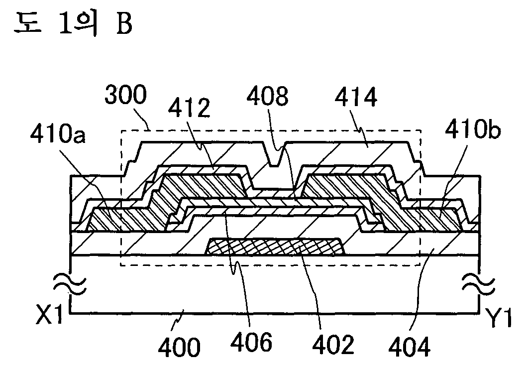
도 1은 트랜지스터(300)의 구조 예를 도시한다. 도 1의 A는 트랜지스터(300)의 평면도이고, 도 1의 B는 도 1의 A에서 1점 쇄선(X1-Y1)을 따라 취해진 단면도이고, 도 1의 C는 도 1의 A에서 1점 쇄선(V1-W1)을 따라 취해진 단면도이다.1 shows an example of a structure of a
트랜지스터(300)는, 절연 표면을 갖는 기판(400) 위의 게이트 전극 층(402), 게이트 전극 층(402) 위의 게이트 절연 층(404), 게이트 절연 층(404) 위의 산화물 절연 층(406), 산화물 절연 층(406) 위에서 산화물 절연 층(406)과 접촉하고 게이트 전극 층(402)과 중첩하는 산화물 반도체 층(408), 및 산화물 반도체 층(408)과 전기적으로 연결된 소스 전극 층(410a) 및 드레인 전극 층(410b)을 포함한다.The
트랜지스터(300)에서, 게이트 절연 층(404)은 질소를 함유하는 실리콘 막을 포함한다. 질소를 함유하는 실리콘 막은 산화 실리콘 막보다 높은 비유전율을 갖고, 등가의 커패시턴스를 위해 더 두꺼운 두께를 필요로 한다. 따라서, 게이트 절연 층의 물리적인 두께는 증가할 수 있다. 이것은 트랜지스터(300)의 내전압의 감소를 줄일 수 있고, 추가로 내전압을 증가시킬 수 있고, 이에 의해 반도체 장치에 대한 정전기 방전 손상을 감소시킨다.In the
게이트 절연 층(404)의 두께는 적어도 산화물 절연 층(406)의 두께보다 두껍고, 바람직하게는 325nm 이상 550nm 이하, 보다 바람직하게는 355nm 이상 550nm 이하이다.The thickness of the
질소를 함유하는 실리콘 막의 예들은, 질화 실리콘 막, 질화산화 실리콘 막, 산화질화 실리콘 막, 등을 포함한다. 높은 질소 함량을 갖는 재료가 더 높은 비유전율을 갖기 때문에, 질화 실리콘 막을 사용하는 것이 바람직하다. 산화 실리콘은 8eV의 에너지 갭을 갖고, 반면 질화 실리콘은 5.5eV의 작은 에너지 갭을 갖고, 따라서 낮은 저항률을 갖는다. 따라서 질화 실리콘 막의 사용은 ESD에 대한 저항을 증가시킬 수 있다. 덧붙여, 질화 실리콘 막이 CVD 방법에 의해 형성되는 경우, 질화산화 실리콘 막과 같이 산소와 질소를 함유하는 실리콘 막이 CVD 방법에 의해 형성될 때 사용되고, 온실 가스인, N2O 가스를 사용할 필요가 없다. 본 명세서에서, "산화질화 실리콘 막"은 질소보다 산소를 더 많이 함유하는 막을 언급하고, "질화산화 실리콘 막"은 산소보다 질소를 더 많이 함유하는 막을 언급함을 주목해야 한다.Examples of the silicon film containing nitrogen include a silicon nitride film, a silicon nitride oxide film, a silicon oxynitride film, and the like. Since a material with a high nitrogen content has a higher relative dielectric constant, it is preferable to use a silicon nitride film. Silicon oxide has an energy gap of 8 eV, whereas silicon nitride has a small energy gap of 5.5 eV, and thus has a low resistivity. Therefore, the use of a silicon nitride film can increase the resistance to ESD. In addition, when the silicon nitride film is formed by the CVD method, it is used when a silicon film containing oxygen and nitrogen, such as a silicon nitride oxide film, is formed by the CVD method, and there is no need to use N 2 O gas, which is a greenhouse gas. It should be noted that in this specification, "silicon oxynitride film" refers to a film containing more oxygen than nitrogen, and "silicon nitride oxide film" refers to a film containing more nitrogen than oxygen.
트랜지스터(300)에서, 산화물 절연 층(406)은 산화물 반도체 층(408)의 구성 원소들로부터 선택된 하나 이상의 금속 원소들을 함유한다. 산화물 절연 층(406)이 이러한 재료를 사용하여 형성되기 때문에, 산화물 절연 층(406)과 산화물 반도체 층(408) 사이의 계면을 안정시킬 수 있고, 계면에서 전하 포획을 줄일 수 있다. 따라서, 트랜지스터의 열화, 특히 광열화를 방지할 수 있고, 따라서 높은 신뢰성의 트랜지스터를 획득할 수 있다.In
특히, 산화물 절연 층(406)으로서, 예컨대 산화 갈륨 막(GaOx(x는 반드시 자연수일 필요는 없고, 비자연수일 수 있음을 주목해야 한다)로도 언급됨), 산화 갈륨 아연 막(Ga2ZnxOy(x=1 내지 5)로도 언급됨, Ga2O3(Gd2O3)막), 높은 갈륨 함량과 낮은 인듐 함량을 갖는 In-Ga-Zn계 산화물 절연 막, 등을 제공하는 것이 바람직하다.In particular, as the
산화물 절연 층(406)과 산화물 반도체 층(408)은 동일한 구성 원소들의 상이한 조성들을 가질 수 있다. 예컨대, In-Ga-Zn계 산화물 반도체 층이 산화물 반도체 층(408)으로 사용되는 경우, 에너지 갭이 인듐(In)과 갈륨(Ga) 사이의 비율에 의해 제어될 수 있으므로, 산화물 반도체 층(408)은 In:Ga:Zn=1:1:1 또는 In:Ga:Zn=3:1:2의 원자 비율을 가질 수 있고, 산화물 절연 층(406)은 In:Ga:Zn=1:3:2의 원자 비율을 가질 수 있다. 산화물 절연 층(406)과 산화물 반도체 층(408)이 스퍼터링 방법에 의해 형성될 수 있고, 인듐을 함유하는 스퍼터링 타깃을 통해, 막 형성 도중의 입자들의 생성이 감소될 수 있음을 주목해야 한다. 따라서, 인듐을 함유하는 산화물 절연 층(406)과 인듐을 함유하는 산화물 반도체 층(408)이 바람직하다.The
도 1에 도시된 트랜지스터(300)의 예에서, 산화물 반도체 층(408)을 섬 형태로 처리하기 위한 에칭 처리를 통해, 산화물 절연 층(406)이 또한 섬 형태로 처리됨을 주목해야 한다. 따라서, 산화물 절연 층(406)과 산화물 반도체 층(408)의 단부들은 서로 배향된다. It should be noted that in the example of the
산화물 반도체 층의 구조는 아래에 기술된다.The structure of the oxide semiconductor layer is described below.
산화물 반도체 층은 대략 단결정 산화물 반도체 층과 비-단결정 산화물 반도체 층으로 분류된다. 비-단결정 산화물 반도체 층은 비정질 산화물 반도체 층, 미결정 산화물 반도체 층, 다결정 산화물 반도체 층, c-축 배향 결정 산화물 반도체(CAAC-OS) 막, 등 중 어느 하나를 포함한다.The oxide semiconductor layer is roughly classified into a single crystal oxide semiconductor layer and a non-single crystal oxide semiconductor layer. The non-single crystal oxide semiconductor layer includes any one of an amorphous oxide semiconductor layer, a microcrystalline oxide semiconductor layer, a polycrystalline oxide semiconductor layer, a c-axis oriented crystal oxide semiconductor (CAAC-OS) film, and the like.
비정질 산화물 반도체 층은 불규칙한 원자 배향을 갖고, 결정 성분을 전혀 갖지 않는다. 이의 전형적인 예는 미소 영역에서 조차 결정부를 전혀 갖지 않고, 층의 전체가 비정질인, 산화물 반도체 층이다.The amorphous oxide semiconductor layer has an irregular atomic orientation and has no crystal components at all. A typical example of this is an oxide semiconductor layer, which has no crystal parts even in a small region, and the entire layer is amorphous.
미결정 산화물 반도체 층은 예컨대 1nm 이상 10nm 미만의 크기를 갖는 미결정(나노결정이라고도 함)을 포함한다. 따라서, 미결정 산화물 반도체 층은 비정질 산화물 반도체 층보다 높은 정도의 원자 규칙성을 갖는다. 따라서, 미결정 산화물 반도체 층의 결함 상태들의 밀도는 비정질 산화물 반도체 층의 밀도보다 낮다.The microcrystalline oxide semiconductor layer includes microcrystals (also referred to as nanocrystals) having a size of 1 nm or more and less than 10 nm, for example. Thus, the microcrystalline oxide semiconductor layer has a higher degree of atomic regularity than the amorphous oxide semiconductor layer. Accordingly, the density of the defect states of the microcrystalline oxide semiconductor layer is lower than that of the amorphous oxide semiconductor layer.
CAAC-OS 막은, 복수의 결정부들을 포함하고, 대부분의 각 결정부가 한 측면이 100nm 미만인 입방체 내에 들어가는 산화물 반도체 층들 중 하나이다. 따라서, CAAC-OS 막 내에 포함된 결정부가, 10nm 미만, 5nm 미만, 또는 3nm 미만인 한 측면을 갖는 입방체 내에 들어가는 경우가 존재한다. CAAC-OS 막의 결함 상태들의 밀도는 미결정 산화물 반도체 층의 것보다 낮다. CAAC-OS 막은 아래에서 상세하게 기술된다.The CAAC-OS film includes a plurality of crystal portions, and most of each crystal portion is one of oxide semiconductor layers that fit into a cube whose one side is less than 100 nm. Accordingly, there is a case where the crystal part contained in the CAAC-OS film enters a cube having one side of less than 10 nm, less than 5 nm, or less than 3 nm. The density of the defect states of the CAAC-OS film is lower than that of the microcrystalline oxide semiconductor layer. The CAAC-OS membrane is described in detail below.
CAAC-OS 막의 투과 전자 현미경(TEM) 이미지에서, 결정부들 사이의 경계, 즉 결정입계는 명확하게 관찰되지 않는다. 따라서, CAAC-OS 막 내에서, 결정입계로 인한 전자 이동도 내의 감소는 발생하기 어렵다.In the transmission electron microscopy (TEM) image of the CAAC-OS film, the boundary between the crystal parts, that is, the grain boundary is not clearly observed. Therefore, in the CAAC-OS film, a decrease in electron mobility due to grain boundaries is unlikely to occur.
샘플 표면에 실질적으로 평행한 방향에서 관찰된 CAAC-OS 막의 TEM 이미지(단면 TEM 이미지)에 따라, 금속 원자들은 결정부들 내에서 층상으로 배열된다. 각 금속 원자 층은 CAAC-OS막이 형성되는 표면(이후로, CAAC-OS막이 형성되는 표면을 피형성면이라 칭한다) 또는 CAAC-OS막의 상면을 반영한 지형을 갖고, CAAC-OS막의 피형성면 또는 상면에 평행하게 배열된다.According to the TEM image (cross-sectional TEM image) of the CAAC-OS film observed in a direction substantially parallel to the sample surface, the metal atoms are arranged in layers in the crystal parts. Each metal atomic layer has a topography reflecting the surface on which the CAAC-OS film is formed (hereinafter, the surface on which the CAAC-OS film is formed is referred to as the surface to be formed) or the top surface of the CAAC-OS film, and the surface on which the CAAC-OS film is formed or It is arranged parallel to the top surface.
본 명세서에 있어서, 용어, "평행"은 2개의 직선들 사이에 형성된 각도가 -10° 이상 10°이하인 것을 말하고, 따라서 각도가 -5° 이상 5° 이하인 경우도 또한 포함한다. 덧붙여, 용어, "수직"이란 2개의 직선들 사이에서 형성된 각도가 80°이상 100°이하인 것을 말하고, 따라서, 각도가 85°이상 95°이하인 경우를 포함한다. In the present specification, the term "parallel" means that an angle formed between two straight lines is -10° or more and 10° or less, and therefore, also includes a case where the angle is -5° or more and 5° or less. In addition, the term "vertical" means that the angle formed between two straight lines is 80° or more and 100° or less, and thus includes the case where the angle is 85° or more and 95° or less.
다른 한 편으로, 샘플 표면에 실질적으로 수직인 방향에서 관찰된 CAAC-OS막의 TEM 이미지(평면 TEM 이미지)에 따라, 금속 원자들은 결정부들 내에서 삼각형 또는 육각형 구성으로 배열된다. 그러나, 상이한 결정부들 사이에서 금속 원자들의 배열의 규칙성은 존재하지 않는다.On the other hand, according to the TEM image (planar TEM image) of the CAAC-OS film observed in a direction substantially perpendicular to the sample surface, the metal atoms are arranged in a triangular or hexagonal configuration within the crystal parts. However, there is no regularity of the arrangement of metal atoms between different crystal parts.
단면 TEM 이미지 및 평면 TEM 이미지의 결과들로부터, CAAC-OS막 내의 결정부들 내에서 배향이 발견된다.From the results of the cross-sectional TEM image and the planar TEM image, the orientation is found in the crystal parts in the CAAC-OS film.
CAAC-OS막은 X선 회절(XRD) 장치를 통한 구조 해석을 받는다. 예컨대, InGaZnO4 결정을 포함하는 CAAC-OS막이 아웃-오브-플레인(out-of-plane)법에 의해 분석될 때, 회절각(2θ)이 대략 31°일 때 피크가 빈번하게 나타난다. 이 피크는, InGaZnO4의 결정의 (009)면으로부터 유도되고, 이는 CAAC-OS막 내의 결정들이 c-축 배향을 갖고, c-축들이 CAAC-OS막의 피형성면 또는 상면에 실질적으로 수직인 방향으로 배향되는 것을 나타낸다.The CAAC-OS film is subjected to structural analysis through an X-ray diffraction (XRD) device. For example, when a CAAC-OS film including an InGaZnO 4 crystal is analyzed by an out-of-plane method, a peak frequently appears when the diffraction angle 2θ is approximately 31°. This peak is derived from the (009) plane of the crystal of InGaZnO 4 , which means that the crystals in the CAAC-OS film have a c-axis orientation, and the c-axis are substantially perpendicular to the formation surface or top surface of the CAAC-OS film. Indicates oriented in a direction.
다른 한 편으로, CAAC-OS막이 c-축에 수직인 방향으로 X선이 샘플로 입사하는 인-플레인(in-plane)법을 통해 분석될 때, 2θ가 대략 56°일 때 피크가 빈번하게 나타난다. 이 피크는 InGaZnO4 결정의 (110)면으로부터 유도된다. 여기에서, 2θ가 대략 56°에서 고정된 상태로, 샘플이 샘플 표면의 법선 벡터를 축(φ축)으로 하여 회전하는 조건들 하에서 분석(φ 스캔)이 수행된다. 샘플이 InGaZnO4의 단결정 산화물 반도체 층인 경우, 6개의 피크들이 출현한다. 6개의 피크들은 (110)면에 등가인 결정 면들로부터 유도된다. 다른 한 편으로, CAAC-OS막의 경우, 2θ가 대략 56°에 고정된 상태에서 φ 스캔이 수행될 때조차, 피크는 명료하게 관찰되지 않는다.On the other hand, when the CAAC-OS film is analyzed by an in-plane method in which X-rays are incident on the sample in a direction perpendicular to the c-axis, the peak frequently occurs when 2θ is approximately 56°. appear. This peak is derived from the (110) plane of the InGaZnO 4 crystal. Here, analysis (φ scan) is performed under conditions in which 2θ is fixed at approximately 56°, and the sample rotates with the normal vector of the sample surface as an axis (φ axis). When the sample is a single crystal oxide semiconductor layer of InGaZnO 4, six peaks appear. The six peaks are derived from crystal planes equivalent to the (110) plane. On the other hand, in the case of the CAAC-OS film, even when a φ scan is performed with 2θ fixed at approximately 56°, the peak is not clearly observed.
위의 결과들에 따라, c-축 배향을 갖는 CAAC-OS막에서, a-축들 및 b-축들의 방향들이 결정부들 사이에서 상이하지만, c-축들은 피형성면의 법선 벡터 또는 상면의 법선 벡터에 평형한 방향으로 배향된다. 따라서, 단면 TEM 이미지에서 관찰된 층상으로 배열된 각 금속 원자 층은 결정의 a-b면에 평행한 면에 대응한다.According to the above results, in a CAAC-OS film having a c-axis orientation, the directions of the a-axis and the b-axis are different between the crystal parts, but the c-axis is the normal vector of the surface to be formed or the normal of the top surface. Oriented in a direction parallel to the vector. Thus, each layer of metal atoms arranged in layers observed in the cross-sectional TEM image corresponds to a plane parallel to the a-b plane of the crystal.
결정부가 CAAC-OS막의 증착과 동시에 형성되거나, 또는 열처리와 같은 결정화 처리를 통해 형성됨을 주목해야 한다. 상술한 바와 같이, 결정의 c-축은 피형성면의 법선 벡터 또는 상면의 법선 벡터에 평행한 방향으로 배향된다. 따라서, 예컨대 CAAC-OS막의 형태가 에칭 등에 의해 변화되는 경우, c-축은 반드시 CAAC-OS막의 피형성면의 법선 벡터 또는 상면의 법선 벡터에 반드시 평행한 것은 아닐 수 있다.It should be noted that the crystal portion is formed simultaneously with the deposition of the CAAC-OS film, or is formed through a crystallization treatment such as heat treatment. As described above, the c-axis of the crystal is oriented in a direction parallel to the normal vector of the surface to be formed or the normal vector of the upper surface. Therefore, for example, when the shape of the CAAC-OS film is changed by etching or the like, the c-axis may not necessarily be parallel to the normal vector of the surface to be formed or the normal vector of the upper surface of the CAAC-OS film.
더욱이, CAAC-OS막 내의 결정화 정도는 반드시 균일한 것은 아니다. 예컨대, CAAC-OS막을 초래하는 결정 성장이 막의 상면의 근처로부터 발생하는 경우, 상면 근처에서 결정화 정도는 일부 경우들에서 피형성면의 근처에서의 결정화 정도보다 높다. 더욱이, CAAC-OS막에 불순물이 첨가될 때, 불순물이 첨가되는 영역 내의 결정화는 변화되고, CAAC-OS막 내의 결정화 정도는 영역들에 따라 변한다.Moreover, the degree of crystallization in the CAAC-OS film is not necessarily uniform. For example, when crystal growth resulting in the CAAC-OS film occurs near the upper surface of the film, the degree of crystallization near the upper surface is higher than the degree of crystallization near the surface to be formed in some cases. Moreover, when an impurity is added to the CAAC-OS film, the crystallization in the region to which the impurity is added changes, and the degree of crystallization in the CAAC-OS film varies depending on the regions.
InGaZnO4 결정을 갖는 CAAC-OS막이 아웃-오브-플레인 법에 의해 분석될 때, 2θ의 피크가 또한 대략 31°에서 2θ의 피크에 부가하여, 대략 36°에서 관찰될 수 있음을 주목해야 한다. 대략 36°에서 2θ의 피크는 c-축 배향을 갖지 않는 결정이 CAAC-OS막의 부분 내에 포함되는 것을 나타낸다. CAAC-OS막 내에서, 2θ의 피크가 대략 31°에서 출현하고, 2θ의 피크가 대략 36°에서 출현하지 않는 것이 바람직하다.It should be noted that when the CAAC-OS film with InGaZnO 4 crystals is analyzed by the out-of-plane method, a peak of 2θ can also be observed at about 36°, in addition to the peak of 2θ at about 31°. A peak of 2θ at approximately 36° indicates that a crystal having no c-axis orientation is included in a portion of the CAAC-OS film. In the CAAC-OS film, it is preferable that the peak of 2θ appears at approximately 31° and the peak of 2θ does not appear at approximately 36°.
본 명세서에서, 삼방정계 또는 능면체정계는 육방정계 내에 포함된다.In the present specification, the trigonal system or rhombohedral system is included in the hexagonal system.
CAAC-OS 막을 사용하는 트랜지스터에서, 가시광 또는 자외광의 조사로 인한 전기 특성들의 변화는 작다. 따라서, 트랜지스터는 높은 신뢰도를 갖는다.In a transistor using a CAAC-OS film, the change in electrical properties due to irradiation of visible light or ultraviolet light is small. Therefore, the transistor has high reliability.
산화물 반도체 층(408)이 예컨대 비정질 산화물 반도체 층, 미결정 산화물 반도체 층, 또는 CAAC-OS 막 중 임의의 구조가 될 수 있거나, 또는 이들의 혼합된 막, 또는 이들 구조들 중 둘 이상의 막들을 포함하는 적층 막일 수 있음을 주목해야 한다.The
일부 경우들에서, 산화물 절연 층(406)은 산화물 반도체 층(408)보다 낮은 결정화도를 가짐을 주목해야 한다. 산화물 절연 층(406)은 비정질부 또는 나노결정을 포함할 수 있다.It should be noted that in some cases,
다른 구성요소들로서, 트랜지스터(300)는 소스 전극 층(410a) 및 드레인 전극 층(410b)을 덮고, 산화물 반도체 층(408)과 접촉하는 산화물 절연 층(412) 및/또는 산화물 절연 층(412) 위의 보호 절연 층(414)을 포함할 수 있다.As other components, the
산화물 절연 층(412)으로, 산화물 절연 층(406)과 같이, 산화물 반도체 층(408)의 구성 원소들로부터 선택된 하나 이상의 금속 원소들을 함유하는 층을 사용하는 것이 바람직하다. 이러한 재료가 사용될 때, 산화물 절연 층(412)과 산화물 반도체 층(408) 사이의 계면을 안정시키는 것이 가능하다. 산화물 절연 층(412)이 산화물 반도체 층(408)의 백 채널 측과 접촉하는 절연 층이기 때문에, 두 층들 사이의 계면에서 전하 포획은 감소되고, 이에 의해 기생 채널의 생성이 줄어들 수 있다. As the
덧붙여, 산화물 반도체 층(408)의 구성 원소들로부터 선택된 하나 이상의 금속 원소들을 함유하는 산화물 절연 층들이 산화물 반도체 층(408)이 사이에 개재되도록 산화물 반도체 층(408)과 접촉하여 산화물 반도체 층(408)의 위와 아래에 제공될 때, 산화물 절연 층들이 산화물 반도체 층에 악영향을 미칠 수 있는 불순물들(질소 및 금속 원소들과 같은)의 확산에 의한 외부로부터의 진입을 차단하도록 작용할 수 있다. 따라서, 산화물 반도체 층이 개재되도록 또는 둘러싸이도록 산화물 절연 층들이 제공될 때, 둘러싸인 산화물 반도체 층의 조성 및 순도는 일정하게 유지될 수 있고, 안정된 전기 특성들을 갖는 반도체 장치가 얻어질 수 있다.In addition, oxide insulating layers containing one or more metal elements selected from the constituent elements of the
보호 절연 층(414)으로서, 산화 실리콘 막, 산화 갈륨 막, 산화 알루미늄 막, 질화 실리콘 막, 산화질화 실리콘 막, 산화질화 알루미늄 막, 질화산화 실리콘 막, 등이 사용될 수 있다.As the protective insulating
<반도체 장치의 구조 예 2><Structure Example 2 of a semiconductor device>
도 2는 트랜지스터(310)의 구조 예를 도시한다. 도 2의 A는 트랜지스터(310)의 평면도이고, 도 2의 B는 도 2의 A에서 1점 쇄선(X2-Y2)을 따라 취해진 단면도이고, 도 2의 C는 도 2의 A에서 1점 쇄선(V2-W2)을 따라 취해진 단면도이다.2 shows an example of the structure of the
도 1의 트랜지스터(300)와 같이, 도 2의 트랜지스터(310)는, 절연 표면을 갖는 기판(400) 위의 게이트 전극 층(402), 게이트 전극 층(402) 위의 게이트 절연 층(404), 게이트 절연 층(404) 위의 산화물 절연 층(406), 산화물 절연 층(406) 위에서 산화물 절연 층(406)과 접촉하고, 게이트 전극 층(402)과 중첩하는 산화물 반도체 층(408), 및 산화물 반도체 층(408)에 전기적으로 연결된 소스 전극 층(410a) 및 드레인 전극 층(410b)을 포함한다. 다른 구성요소들로서, 트랜지스터(310)는 소스 전극 층(410a) 및 드레인 전극 층(410b)을 덮고, 산화물 반도체 층(408)과 접촉하는 산화물 절연 층(412) 및 산화물 절연 층(412) 위의 보호 절연 층(414)을 포함할 수 있다.Like the
트랜지스터(310)는 게이트 절연 층(404)과 산화물 반도체 층(408)의 구조들에서 트랜지스터(300)와 다르다. 즉, 트랜지스터(310) 내의 게이트 절연 층(404)은 게이트 전극 층(402)과 접촉하는 게이트 절연 층(404a)과 게이트 절연 층(404a)과 산화물 절연 층(406) 사이의 게이트 절연 층(404b)을 포함한다. 트랜지스터(310) 내의 산화물 반도체 층(408)은 산화물 절연 층(406)과 접촉하는 산화물 반도체 층(408a)과 산화물 절연 층(412)과 접촉하는 산화물 반도체 층(408b)을 포함한다. 트랜지스터(310) 내의 게이트 절연 층(404)과 산화물 반도체 층(408) 이외의 다른 구성요소들이 트랜지스터(300)의 다른 구성요소들과 유사하고, 이를 위해 트랜지스터(300)의 설명이 인용될 수 있음을 주목해야 한다.
트랜지스터(310)에서, 게이트 절연 층(404a)과 게이트 절연 층(404b)은 각각 질화 실리콘 막을 포함한다.In the
게이트 절연 층(404a)은 게이트 절연 층(404b)보다 더 두꺼운 두께를 갖고, 더 적은 수의 결함들을 포함하는 질화 실리콘 막을 포함한다. 예컨대, 게이트 절연 층(404a)의 두께는 300nm 이상 400nm 이하이다. 덧붙여, 전자 스핀 공명(ESR) 분광법에서 Nc 중심에서(2.003의 g 계수에서) 나타나는 신호에 대응하는 1×10¹⁷spins//㎤ 이하, 바람직하게는 5×10¹⁶spins/㎤ 이하의 스핀 밀도를 갖는 질화 실리콘 막이 사용된다. 두꺼운 두께(예, 300nm 이상)를 갖고, 적은 수의 결함들을 포함하는 이러한 질화 실리콘 막이 제공될 때, 게이트 절연 층(404a)의 내전압은 예컨대 300V 이상이 될 수 있다.The
게이트 절연 층(404b)이 산화물 반도체 층(408)과 접촉하기 때문에, 게이트 절연 층(404b)은 낮은 농도의 수소를 함유하는 질화 실리콘 막을 포함하여야 하고, 수소 농도는 적어도 게이트 절연 층(404a)의 수소 농도보다 낮아야 한다. 예컨대, 게이트 절연 층(404a)과 게이트 절연 층(404b)이 플라즈마 CVD 방법에 의해 형성되는 경우, 게이트 절연 층(404b)의 수소 농도는 공급 가스 내에 함유된 수소의 농도를 감소시킴으로써 게이트 절연 층(404a)의 수소 농도보다 낮게 이루어질 수 있다. 특히, 질화 실리콘 막들이 게이트 절연 층(404a)과 게이트 절연 층(404b)으로서 형성되는 경우, 게이트 절연 층(404b)은 게이트 절연 층(404a)을 형성하기 위한 공급 가스 내에서보다 더 낮은 암모니아 유동율로 형성될 수 있거나, 또는 암모니아를 사용하지 않고 형성될 수 있다.Since the
게이트 절연 층(404b)의 두께는 25nm 이상 150nm 이하이다. 낮은 농도의 수소를 함유하는 질화 실리콘 막이 게이트 절연 층(404b)으로서 제공되기 때문에, 산화물 절연 층(406) 및 산화물 반도체 층(408)으로 수소 또는 수소 화합물(예, 물)의 진입을 줄이는 것이 가능하다. 산화물 반도체 내의 수소는 캐리어들이 생성되게 하고, 트랜지스터의 문턱 전압이 음의 방향으로 이동하게 한다. 따라서, 낮은 수소 농도를 갖는 질화 실리콘 막이 게이트 절연 층(404b)으로서 제공될 때, 트랜지스터의 전기 특성들은 안정화될 수 있다. 덧붙여, 낮은 수소 농도를 갖는 질화 실리콘 막이 게이트 절연 층(404b)으로서 제공될 때, 게이트 절연 층(404b)은 또한, 게이트 절연 층(404a) 내에 함유된 수소 또는 수소 화합물과 같은 불순물들이 산화물 절연 층(406) 및 산화물 반도체 층(408)으로 확산되는 것을 방지하기 위한 장벽 막으로서 작용한다.The thickness of the
본 실시예에서 게이트 절연 층(404a)과 게이트 절연 층(404b) 모두 질화 실리콘 막들이고, 이들 게이트 절연 층들 사이의 계면이 재료들 또는 막 형성 조건들에 따라 불명확하게 될 수 있음을 주목해야 한다. 따라서, 도 2의 B 및 C에서, 게이트 절연 층(404a)과 게이트 절연 층(404b) 사이의 계면은 개략적으로 점선으로 도시된다. 아래에 기술된 다른 도면들에 대해서도 동일하다.It should be noted that in this embodiment, both the
산화물 반도체 층(408) 내에 포함된 산화물 반도체 층(408a)과 산화물 반도체 층(408b)은 동일한 구성 원소들의 상이한 조성들을 갖는 것이 바람직하다. 인듐과 갈륨을 함유하는 산화물 반도체 층들이 산화물 반도체 층(408a)과 산화물 반도체 층(408b)으로 형성되는 경우, 게이트 전극 층(402)에 근접한 측(채널 측) 상의 산화물 반도체 층(408a) 내에서 인듐의 함량이 갈륨의 함량보다 높은(In > Ga) 것이 바람직하다. 또한, 게이트 전극 층(402)으로부터 먼 측(백 채널 측) 상의 산화물 반도체 층(408b) 내에서 인듐의 함량은 갈륨의 함량 이하인(In ≤ Ga) 것이 바람직하다.It is preferable that the
산화물 반도체에서, 중금속의 s 궤도는 주로 캐리어 전도에 기여하고, 산화물 반도체 내의 인듐 함량이 증가할 때 s 궤도들의 중첩들은 증가하기 쉽다. 그러므로, In > Ga의 조성을 갖는 산화물은 In ≤ Ga의 조성을 갖는 산화물보다 더 높은 이동도를 갖는다. 더욱이, Ga에서, 산소의 빈자리의 형성 에너지는 더 크고, 따라서 산소의 빈자리들은 In 내에서보다 생성되기 어렵고; 따라서 In ≤ Ga의 조성을 갖는 산화물은 In > Ga의 조성을 갖는 산화물보다 더 안정된 특성들을 갖는다.In an oxide semiconductor, the s orbitals of the heavy metal mainly contribute to carrier conduction, and the overlaps of the s orbitals tend to increase when the indium content in the oxide semiconductor increases. Therefore, an oxide having a composition of In> Ga has a higher mobility than an oxide having a composition of In? Ga. Moreover, in Ga, the formation energy of oxygen vacancies is larger, and thus oxygen vacancies are more difficult to generate than in In; Therefore, an oxide having a composition of In ≤ Ga has more stable properties than an oxide having a composition of In> Ga.
In > Ga의 조성을 갖는 산화물 반도체는 채널 측 상에서 사용되고, In ≤ Ga의 조성을 갖는 산화물 반도체는 백 채널 측 상에서 사용되어, 트랜지스터의 이동도와 신뢰도는 추가로 개선될 수 있다. 예컨대, 산화물 반도체 층(408a)은 In:Ga:Zn = 3:1:2의 원자 비율을 가질 수 있고, 산화물 반도체 층(408b)은 In:Ga:Zn = 1:1:1의 원자 비율을 가질 수 있다.An oxide semiconductor having a composition of In>Ga is used on the channel side, and an oxide semiconductor having a composition of In≦Ga is used on the back channel side, so that the mobility and reliability of the transistor can be further improved. For example, the
산화물 반도체 층(408a) 및 산화물 반도체 층(408b)과 접촉하는 산화물 절연 층(406)이 동일한 구성 원소들의 상이한 조성들을 가져, 두 층의 계면이 추가로 안정화될 수 있기 때문에 산화물 절연 층(406)이 절연 특성을 갖는 것이 바람직함을 주목해야 한다. 산화물 반도체 층(408b)과 접촉하는 산화물 절연 층(412)에 대해서도 동일하다.The
또한, 상이한 결정도들을 갖는 산화물 반도체들이 산화물 반도체 층(408a) 및 산화물 반도체 층(408b)을 위하여 사용될 수 있다. 즉, 산화물 반도체 층들(408a 및 408b)은 단결정 산화물 반도체, 다결정 산화물 반도체, 나노결정 산화물 반도체, 비정질 산화물 반도체, 및 CAAC-OS 중 임의의 것의 조합을 적절하게 사용하여 형성될 수 있다. 비정질 산화물 반도체는 수소와 같은 불순물들을 흡착하기 쉽고, 산소의 빈자리들을 갖기 쉽고, 따라서 쉽게 n-형이 될 수 있음을 주목해야 한다. 그러므로, 채널 측 상의 산화물 반도체 층(408a)은 CAAC-OS와 같은 결정 산화물 반도체를 사용하여 형성되는 것이 바람직하다.Also, oxide semiconductors having different crystallinities may be used for the
백 채널 측 상의 산화물 반도체 층(408b)이 비정질 산화물 반도체를 사용하여 형성될 때, 산화물 반도체 층(408b)은 소스 전극 층(410a) 및 드레인 전극 층(410b)을 형성하기 위한 에칭 처리를 통해 산소의 빈자리들을 갖기 쉽고, 쉽게 n-형이 된다. 따라서 산화물 반도체 층(408b)이 결정 산화물 반도체를 사용하여 형성되는 것이 바람직하다.When the
도 14는 게이트 절연 층(GI), 산화물 절연 층(OI1), 산화물 반도체 층들(OS1 및 OS2), 산화물 절연 층(OI2), 및 보호 절연 층(Passi)의 적층구조를 갖는 본 실시예에서의 트랜지스터의 에너지 밴드 도면(개략도)이다. 게이트 절연 층, 산화물 절연 층들, 산화물 반도체 층들, 및 보호 절연 층이 모두 진성인 이상적인 상황을 간주하여, 도 14는 게이트 절연 층(GI)과 보호 절연 층(Passi)이 질화 실리콘 막들(밴드 갭(Eg): 5eV)이고, 산화물 절연 층(OI1)과 산화물 절연 층(OI2)이 In:Ga:Zn=1:3:2(밴드 갭(Eg): 3.6eV)인 In-Ga-Zn계 산화물 절연 층들이고, 산화물 반도체 층(OS1)이 In:Ga:Zn=3:1:2(밴드 갭(Eg): 2.8eV)인 In-Ga-Zn계 산화물 반도체 층이고, 산화물 반도체 층(OS2)이 In:Ga:Zn=1:1:1(밴드 갭(Eg): 3.2eV)인 In-Ga-Zn계 산화물 반도체 층인 경우를 도시한다.14 is a diagram in the present embodiment having a stacked structure of a gate insulating layer GI, an oxide insulating layer OI1, oxide semiconductor layers OS1 and OS2, an oxide insulating layer OI2, and a protective insulating layer Passi. It is a diagram (schematic diagram) of the energy band of the transistor. Considering an ideal situation in which the gate insulating layer, the oxide insulating layers, the oxide semiconductor layers, and the protective insulating layer are all intrinsic, FIG. 14 shows that the gate insulating layer GI and the protective insulating layer Passi are silicon nitride films (band gaps). Eg): 5eV), and the oxide insulating layer (OI1) and the oxide insulating layer (OI2) are In:Ga:Zn = 1:3:2 (band gap (Eg): 3.6 eV) In-Ga-Zn oxide Insulation layers, the oxide semiconductor layer (OS1) is an In-Ga-Zn-based oxide semiconductor layer with In:Ga:Zn=3:1:2 (band gap (Eg): 2.8 eV), and an oxide semiconductor layer (OS2) A case of an In-Ga-Zn-based oxide semiconductor layer having an In:Ga:Zn=1:1:1 (band gap (Eg): 3.2 eV) is shown.
도 14에서 산화물 절연 층(OI1), 산화물 절연 층(OI2), 산화물 반도체 층(OS1) 및 산화물 반도체 층(OS2)은 모두 15의 비유전율을 갖는 것으로 가정됨을 주목해야 한다. 또한, 산화물 절연 층(OI1)과 산화물 절연 층(OI2)은 4㎠/Vs의 이동도를 갖고, 산화물 반도체 층(OS1)은 25㎠/Vs의 이동도를 갖고, 산화물 반도체 층(OS2)은 10㎠/Vs의 이동도를 갖는 것으로 간주된다. 더욱이, 게이트 절연 층(GI)이 325nm의 두께를 갖고, 산화물 절연 층(OI1)이 30nm의 두께를 갖고, 산화물 반도체 층(OS1)이 10nm의 두께를 갖고, 산화물 반도체 층(OS2)이 10nm의 두께를 갖고, 산화물 절연 층(OI2)이 30nm의 두께를 갖고, 보호 절연 층(Passi)이 300nm의 두께를 갖는 것으로 간주된다. 이들 가정들에 기초하여 계산이 수행된다.In FIG. 14, it should be noted that the oxide insulating layer OI1, the oxide insulating layer OI2, the oxide semiconductor layer OS1, and the oxide semiconductor layer OS2 are all assumed to have a relative dielectric constant of 15. In addition, the oxide insulating layer OI1 and the oxide insulating layer OI2 have a mobility of 4 cm 2 /Vs, the oxide semiconductor layer OS1 has a mobility of 25 cm 2 /Vs, and the oxide semiconductor layer OS2 It is considered to have a mobility of 10 cm 2 /Vs. Moreover, the gate insulating layer GI has a thickness of 325 nm, the oxide insulating layer OI1 has a thickness of 30 nm, the oxide semiconductor layer OS1 has a thickness of 10 nm, and the oxide semiconductor layer OS2 has a thickness of 10 nm. It is considered that it has a thickness, the oxide insulating layer OI2 has a thickness of 30 nm, and the protective insulating layer Passi has a thickness of 300 nm. Calculations are performed based on these assumptions.
도 14에 도시된 바와 같이, 산화물 반도체 층(OS1)의 게이트 전극 측(채널 측) 상에서, 산화물 반도체 층(OS1)과 산화물 절연 층(OI1) 사이의 계면에 에너지 장벽이 존재한다. 유사하게, 산화물 반도체 층(OS2)의 백 채널 측(게이트 전극 측의 반대편) 상에서, 산화물 반도체 층(OS2)과 산화물 절연 층(OI2) 사이의 계면에 에너지 장벽이 존재한다. 이러한 에너지 장벽들은 산화물 반도체 층들과 산화물 절연 층들 사이의 계면들에 존재하므로, 계면들에서 캐리어들의 이동은 방지될 수 있고; 따라서 캐리어들은 산화물 반도체 층들 내부에서 이동하고, 산화물 반도체 층들로부터 산화물 절연 층들로 이동하지 않는다. 즉, 산화물 반도체의 밴드 갭보다 계단적으로 큰 밴드 갭들을 갖는 재료들 사이에 산화물 반도체 층들이 개재되도록 적층 구조가 형성될 때, 캐리어들은 산화물 반도체 층(OS1)과 산화물 반도체 층(OS2) 내부에서 이동한다.14, on the gate electrode side (channel side) of the oxide semiconductor layer OS1, an energy barrier exists at the interface between the oxide semiconductor layer OS1 and the oxide insulating layer OI1. Similarly, on the back channel side (opposite of the gate electrode side) of the oxide semiconductor layer OS2, an energy barrier exists at the interface between the oxide semiconductor layer OS2 and the oxide insulating layer OI2. Since these energy barriers exist at the interfaces between the oxide semiconductor layers and the oxide insulating layers, the movement of carriers at the interfaces can be prevented; Thus, carriers move inside the oxide semiconductor layers and do not migrate from the oxide semiconductor layers to the oxide insulating layers. That is, when a stacked structure is formed such that oxide semiconductor layers are interposed between materials having band gaps stepwise larger than the band gap of the oxide semiconductor, carriers move inside the oxide semiconductor layer OS1 and the oxide semiconductor layer OS2. do.
<반도체 장치의 제작 방법><Method of manufacturing semiconductor device>
트랜지스터(310)를 제작하는 방법의 일 예가 도 3을 참조하여 아래에서 기술될 것이다.An example of a method of manufacturing the
먼저, 게이트 전극 층(402)이 절연 표면을 갖는 기판(400) 위에 형성된다. First, a
절연 표면을 갖는 기판(400)으로서 사용될 수 있는 기판에 대한 특별한 제한은 없지만, 기판이 이후에 수행되는 열처리를 견디기에 충분한 열 저항을 갖는 것이 최소한 필요하다. 예컨대, 바륨 붕규산염 유리, 알루미노 붕규산염 유리, 등의 유리 기판, 세라믹 기판, 수정 기판, 사파이어 기판, 등이 사용될 수 있다. 대안적으로, 실리콘, 탄화 실리콘, 등으로 만들어진 단결정 반도체 기판 또는 다결정 반도체 기판, 실리콘 게르마늄, 등으로 만들어진 복합 반도체 기판, SOI 기판, 등이 기판(400)으로 사용될 수 있다. 또 다른 대안으로서, 반도체 소자를 추가로 구비한 이들 기판들 중 임의의 기판이 기판(400)으로 사용될 수 있다.There is no particular limitation on the substrate that can be used as the
게이트 전극 층(402)은 몰리브덴, 티타늄, 탄탈, 텅스텐, 알루미늄, 구리, 크롬, 네오디뮴, 또는 스칸듐, 또는 주 성분으로서 이들 재료들 중 임의의 것을 함유한 합금재료와 같은 금속 재료를 사용하여 형성될 수 있다. 대안적으로, 인과 같은 불순물 원소로 도핑된 다결정 실리콘 막으로 전형화된 반도체 막, 또는 규화 니켈 막과 같은 규화물 막이 게이트 전극 층(402)으로 사용될 수 있다. 게이트 전극 층(402)은 단일층 구조 또는 적층 구조를 가질 수 있다. 게이트 전극 층(402)은 예컨대 30°이상 70°이하의 경사 각도를 갖는 경사진 형태를 가질 수 있다. 여기에서, 경사 각도는 경사진 형태를 갖는 층의 측면 표면과 층의 바닥 표면 사이에 형성된 각도를 언급한다.The
게이트 전극 층(402)의 재료는 산화 인듐 산화 주석, 산화 텅스텐을 함유하는 산화 인듐, 산화 텅스텐을 함유하는 산화 인듐 아연, 산화 티타늄을 함유하는 산화 인듐, 산화 티타늄을 함유하는 산화 인듐 주석, 산화 인듐 산화 아연, 또는 산화 실리콘이 첨가된 산화 인듐 주석과 같은 전도성 재료가 될 수 있다.The material of the
대안적으로, 게이트 전극 층(402)의 재료는 질소를 함유하는 In-Ga-Zn계 산화물, 질소를 함유하는 In-Sn계 산화물, 질소를 함유하는 In-Ga계 산화물, 질소를 함유하는 In-Zn계 산화물, 질소를 함유하는 Sn계 산화물, 질소를 함유하는 In계 산화물, 또는 질화 금속(질화 인듐, 질화 아연, 질화 탄탈, 또는 질화 텅스텐과 같은)이 될 수 있다. 이들 재료들 각각은 5eV 이상의 일함수를 갖고, 이는 게이트 전극 층(402)을 위해 사용될 때 트랜지스터의 문턱 전압이 양이 될 수 있게 한다. 따라서, 정상 오프 스위칭 트랜지스터가 제공될 수 있다.Alternatively, the material of the
다음에, 게이트 절연 층(404a)과 게이트 절연 층(404b)을 포함하는 게이트 절연 층(404)은 게이트 전극 층(402)을 덮도록 형성된다(도 3의 A 참조). 질소를 함유하는 실리콘 막은 게이트 절연 층(404)을 위해 사용될 수 있다. 본 실시예에 있어서, 게이트 절연 층(404)은 질화 실리콘 막을 포함하는 게이트 절연 층(404a)과 질화 실리콘 막을 포함하는 게이트 절연 층(404b)을 적층함으로써 형성된다. 면 내의 변동, 입자들의 혼합, 및 막 형성 주기 시간의 감소를 위해, 게이트 절연 층(404)을 형성하기 위해 CVD 방법을 사용하는 것이 효과적이다. CVD 방법은 또한 대형 기판 위에 막을 형성하는데 효과적이다.Next, a
본 실시예에 있어서, 게이트 절연 층(404a) 및 게이트 절연 층(404b)은 플라즈마 CVD 방법에 의해 연속적으로 형성된다. 먼저, 공급 가스로서 실란(SiH4), 질소(N2) 및 암모니아(NH3)의 혼합 가스를 사용하여, 질화 실리콘 막이 게이트 절연 층(404a)으로서 형성되고, 이후 공급 가스가 실란(SiH4)과 질소(N2)의 혼합 가스로 변경되고, 질화 실리콘 막이 게이트 절연 층(404b)으로서 형성된다.In this embodiment, the
공급 가스로서 실란(SiH4), 질소(N2) 및 암모니아(NH3)의 혼합 가스를 사용하는 플라즈마 CVD 방법에 의해 형성된 질화 실리콘 막은 공급 가스로서 실란(SiH4)과 질소(N2)의 혼합 가스를 사용하여 형성된 질화 실리콘 막보다 더 적은 결함들을 포함한다. 따라서, 게이트 절연 층(404a)은 적어도 게이트 절연 층(404b)보다 더 적은 결함들을 포함하고, 전자 스핀 공명(ESR) 분광법에서 Nc 중심에서(2.003의 g 계수에서) 나타나는 신호에 대응하는 1×10¹⁷spins/㎤ 이하, 바람직하게는 5×10¹⁶spins/㎤ 이하의 스핀 밀도를 가질 수 있다. 암모니아를 포함하는 혼합 가스를 사용하여 형성된 질화 실리콘 막은 공급 가스로서 실란과 질소의 혼합 가스를 사용하여 형성된 것보다 더 양호한 커버리지를 제공한다. 따라서, 게이트 전극 층(402)과 접촉하는 게이트 절연 층으로서, 상술한 혼합 가스를 사용하여 형성된 질화 실리콘 막을 제공하는 것이 효과적이다. 적은 수의 결함들을 포함하는 게이트 절연 층(404a)이 300nm 이상 400nm 이하의 두께를 갖도록 형성될 때, 게이트 절연 층(404)의 내전압은 300V 이상이 될 수 있다.The silicon nitride film formed by the plasma CVD method using a mixed gas of silane (SiH 4 ), nitrogen (N 2 ) and ammonia (NH 3 ) as a supply gas is a combination of silane (SiH 4 ) and nitrogen (N 2 ) as a supply gas. It contains fewer defects than a silicon nitride film formed using a mixed gas. Thus, the
한편, 암모니아를 함유하지 않는 소스 가스를 통해 형성된 게이트 절연 층(404b)은 게이트 절연 층(404a)보다 더 낮은 수소 농도를 함유한다. 25nm 이상 150nm 이하의 두께를 갖는 이러한 막이 산화물 절연 층(406)과 게이트 전극 층(402) 사이에 제공될 때, 게이트 절연 층(404b)으로부터 산화물 절연 층(406) 및 산화물 반도체 층(408)으로의 수소의 진입을 줄일 수 있다. 게이트 절연 층(404b)은 또한 게이트 절연 층(404a)에 함유된 수소 또는 수소 화합물의 산화물 절연 층(406) 및 산화물 반도체 층(408)으로의 진입을 감소시키는 장벽 막으로서 기능한다.On the other hand, the
큰 두께를 갖고, 적은 수의 결함들을 포함하는 게이트 절연 층(404a)과 낮은 수소 농도를 갖는 게이트 절연 층(404b)이 게이트 절연 층(404)으로서 적층될 때, 양호한 내전압을 얻고, 동시에 수소와 같은 불순물의 산화물 절연 층(406) 및 산화물 반도체 층(408)으로의 확산을 감소시키는 것이 가능하다. 따라서, 게이트 절연 층(404)을 포함하는 트랜지스터에 대한 정전기 방전 손상을 줄이고, 이의 전기 특성들을 안정화시키는 것이 가능하다.When the
다음에, 산화물 절연 층과 산화물 반도체 층이 게이트 절연 층(404b) 위에 형성되고, 에칭 처리에 의해 섬 형태로 처리되고, 이에 의해 산화물 절연 층(406), 및 산화물 반도체 층(408a)과 산화물 반도체 층(408b)을 포함하는 산화물 반도체 층(408)이 형성된다(도 3의 B 참조). 하나의 포토마스크를 사용하여 에칭 처리가 수행되기 때문에, 산화물 절연 층(406)과 산화물 반도체 층(408)은 평면도에서 동일한 패턴 형태를 갖고, 이들의 단부들은 서로 배향된다.Next, an oxide insulating layer and an oxide semiconductor layer are formed over the
산화물 절연 층(406)으로서, 산화물 반도체 층(408)의 구성 원소들로부터 선택된 하나 이상의 금속 원소들을 함유하는 산화물 절연 층이 제공된다. 예컨대, 산화 갈륨 막, 산화 갈륨 아연 막, 산화 갈륨 가돌리늄 막, 또는 높은 갈륨 함량과 낮은 인듐 함량을 갖는 In-Ga-Zn계 산화물 절연 막과 같은 절연 막을 사용하는 것이 바람직하다.As the
산화물 반도체 층(408)은 비정질 구조 또는 결정 구조를 가질 수 있다. 형성된 후의 산화물 반도체 층이 비정질 구조를 갖는 경우, 산화물 반도체 층은, 산화물 반도체 층(408)이 결정 구조를 갖도록, 이후의 제조 공정에서 열처리를 받을 수 있다. 비정질 산화물 반도체 층을 결정화하기 위한 열처리는, 250℃ 이상 700℃ 이하, 바람직하게는 400℃ 이상, 더 바람직하게는 500℃ 이상, 추가로 더욱 바람직하게는 550℃ 이상의 온도에서 수행된다. 열처리가 또한 제조 공정 내의 다른 열처리로서 작용할 수 있음을 주목해야 한다.The
산화물 절연 층(406) 및 산화물 반도체 층(408)은 스퍼터링 방법, 분자빔 에피택시(MBE) 방법, CVD 방법, 펄스드 레이저 증착 방법, 원자층 증착(ALD) 방법, 등에 의해 적절하게 형성될 수 있다.The
산화물 절연 층(406) 및 산화물 반도체 층(408)의 형성시, 함유될 수소의 농도는 가능한 한 많이 감소되는 것이 바람직하다. 수소의 농도를 줄이기 위하여, 예컨대, 산화물 절연 층 및 산화물 반도체 층이 스퍼터링 방법에 의해 형성되는 경우, 수소, 물, 수산기 및 수산화물과 같은 불순물들이 제거된 높은 순도의 희 가스(전형적으로 아르곤), 높은 순도의 산소, 또는 희 가스와 산소의 높은 순도의 혼합 가스가 스퍼터링 장치의 막 형성 챔버에 공급되는 대기 가스로서 적절하게 사용된다.When forming the
산화물 절연 층 및 산화물 반도체 층은, 막 형성 챔버 내에 남아 있는 습기가 제거되는 동안, 수소와 습기가 제거된 스퍼터링 가스가 막 형성 챔버 내로 도입되는 방식으로 형성되고, 이에 의해 산화물 절연 층 및 산화물 반도체 층 내의 수소의 농도는 감소될 수 있다. 막 형성 챔버 내에 남아 있는 습기를 제거하기 위하여, 크라이오 펌프, 이온 펌프, 또는 티타늄 승화 펌프와 같은 흡착 진공 펌프가 사용되는 것이 바람직하다. 저온 동결 트랩(cold trap)을 구비한 터보 분자 펌프가 대안적으로 사용될 수 있다. 막 형성 챔버가 수소 분자, 물(H2O)과 같은 수소 원자를 함유한 화합물(바람직하게는 또한 탄소 원자를 포함하는 화합물), 등을 제거하는 높은 성능을 갖는 크라이오 펌프로 배기될 때, 막 형성 챔버 내에서 형성된 막 내에 함유될 불순물 농도는 감소될 수 있다.The oxide insulating layer and the oxide semiconductor layer are formed in such a way that hydrogen and a sputtering gas from which moisture has been removed are introduced into the film forming chamber while the moisture remaining in the film forming chamber is removed, whereby the oxide insulating layer and the oxide semiconductor layer The concentration of hydrogen in the can be reduced. In order to remove moisture remaining in the film forming chamber, it is preferable to use an adsorption vacuum pump such as a cryo pump, an ion pump, or a titanium sublimation pump. Turbomolecular pumps with cold traps can alternatively be used. When the film forming chamber is evacuated to a cryopump with high performance to remove hydrogen molecules, compounds containing hydrogen atoms such as water (H 2 O) (preferably also compounds containing carbon atoms), etc., The concentration of impurities to be contained in the film formed in the film formation chamber can be reduced.
산화물 절연 층 및 산화물 반도체 층이 공기에 노출되지 않고 연속적으로 형성되는 것이 바람직함을 주목해야 한다. 공기에 노출되지 않고 산화물 절연 층 및 산화물 반도체 층의 연속적인 형성에 의해, 수소 또는 수소 화합물(예, 물)은 산화물 절연 층의 표면 또는 그 위에 적층된 산화물 반도체 층의 표면에 부착되는 것이 방지될 수 있다. 따라서, 불순물들의 진입은 감소될 수 있다.It should be noted that it is preferable that the oxide insulating layer and the oxide semiconductor layer are formed continuously without being exposed to air. By the continuous formation of the oxide insulating layer and the oxide semiconductor layer without exposure to air, hydrogen or a hydrogen compound (e.g., water) can be prevented from adhering to the surface of the oxide insulating layer or the surface of the oxide semiconductor layer stacked thereon. I can. Thus, the ingress of impurities can be reduced.
산화물 절연 층 또는 산화물 반도체 층이 스퍼터링 방법에 의해 형성될 때, 막 형성을 위해 사용된 금속 산화물 타깃의 상대적인 밀도(충진 계수)는 90% 이상 100% 이하, 바람직하게는 95% 이상 99.9% 이하이다. 높은 상대 밀도를 갖는 금속 산화물 타깃을 사용하여, 조밀한 산화물 막이 형성될 수 있다.When the oxide insulating layer or oxide semiconductor layer is formed by the sputtering method, the relative density (filling factor) of the metal oxide target used for film formation is 90% or more and 100% or less, preferably 95% or more and 99.9% or less. . By using a metal oxide target having a high relative density, a dense oxide film can be formed.
산화물 반도체 층의 불순물 농도를 줄이기 위하여, 기판(400)이 높은 온도로 유지되는 동안 산화물 반도체 층을 형성하는 것이 또한 효과적임을 주목해야 한다. 기판(400)이 가열되는 온도는 150℃ 이상 450℃ 이하일 수 있고; 기판 온도는 바람직하게는 200℃ 이상 350℃ 이하이다. 결정 산화물 반도체 층은 기판을 형성시에 높은 온도로 가열함으로써 형성될 수 있다.It should be noted that in order to reduce the impurity concentration of the oxide semiconductor layer, it is also effective to form the oxide semiconductor layer while the
CAAC-OS 막이 산화물 반도체 층(408)으로 사용되는 경우, CAAC-OS 막은 다음의 방법들로 얻어질 수 있다. 하나의 방법은 200℃ 이상 450℃ 이하의 막 형성 온도에서 산화물 반도체 층을 형성하는 것이고, 이에 의해 표면에 실질적으로 수직인 c-축 배향을 얻는다. 다른 방법은 얇은 산화물 반도체 층을 형성하고, 이후 이 층을 200℃ 이상 700℃ 이하의 온도로 수행되는 열처리를 받게 하고, 이에 의해 표면에 실질적으로 수직인 c-축 배향을 얻는다. 또 다른 방법은 제 1의 얇은 산화물 반도체 막을 형성하고, 이 막을 200℃ 이상 700℃ 이하의 온도로 수행되는 열처리를 받게 하고, 이후 제 2 산화물 반도체 막을 형성하고, 이에 의해 표면에 실질적으로 수직인 c-축 배향을 얻는다.When the CAAC-OS film is used as the
산화물 반도체 층(408)을 위해 사용된 산화물 반도체는 적어도 인듐(In)을 함유한다. 특히, 인듐과 아연(Zn)이 바람직하게 함유된다. 덧붙여, 산화물 반도체를 사용하는 트랜지스터의 전기 특성들의 변동을 줄이기 위한 안정제로서, 갈륨(Ga)이 추가적으로 함유되는 것이 바람직하다. 주석(Sn), 하프늄(Hf), 알루미늄(Al) 및 지르코늄(Zr)으로부터 선택된 하나 이상의 원소들이 안정제로서 함유되는 것이 바람직하다.The oxide semiconductor used for the
다른 안정제로서, 란탄(La), 세륨(Ce), 프라세오디뮴(Pr), 네오디뮴(Nd), 사마륨(Sm), 유러퓸(Eu), 가돌리늄(Gd), 테르븀(Tb), 디스프로슘(Dy), 홀뮴(Ho), 에르븀(Er), 튤륨(Tm), 이테르븀(Yb), 및 루테튬(Lu)으로부터 선택된 하나 이상의 란탄족원소가 함유될 수 있다.As other stabilizers, lanthanum (La), cerium (Ce), praseodymium (Pr), neodymium (Nd), samarium (Sm), europium (Eu), gadolinium (Gd), terbium (Tb), dysprosium (Dy), One or more lanthanide elements selected from holmium (Ho), erbium (Er), thulium (Tm), ytterbium (Yb), and lutetium (Lu) may be contained.
산화물 반도체로서, 예컨대, 산화 인듐, 산화 주석, 산화 아연, 2-원소 금속의 산화물인 In-Zn계 산화물, In-Mg계 산화물 또는 In-Ga계 산화물, 3-원소 금속의 산화물인 In-Ga-Zn계 산화물, In-Al-Zn계 산화물, In-Sn-Zn계 산화물, In-Hf-Zn계 산화물, In-La-Zn계 산화물, In-Ce-Zn계 산화물, In-Pr-Zn계 산화물, In-Nd-Zn계 산화물, In-Sm-Zn계 산화물, In-Eu-Zn계 산화물, In-Gd-Zn계 산화물, In-Tb-Zn계 산화물, In-Dy-Zn계 산화물, In-Ho-Zn계 산화물, In-Er-Zn계 산화물, In-Tm-Zn계 산화물, In-Yb-Zn계 산화물 또는 In-Lu-Zn계 산화물, 또는 4-원소 금속 산화물인 In-Sn-Ga-Zn계 산화물, In-Hf-Ga-Zn계 산화물, In-Al-Ga-Zn계 산화물, In-Sn-Al-Zn계 산화물, In-Sn-Hf-Zn계 산화물 또는 In-Hf-Al-Zn계 산화물이 사용될 수 있다.As an oxide semiconductor, for example, indium oxide, tin oxide, zinc oxide, an In-Zn-based oxide that is an oxide of a two-element metal, an In-Mg-based oxide or an In-Ga-based oxide, and an In-Ga that is an oxide of a three-element metal. -Zn-based oxide, In-Al-Zn-based oxide, In-Sn-Zn-based oxide, In-Hf-Zn-based oxide, In-La-Zn-based oxide, In-Ce-Zn-based oxide, In-Pr-Zn Oxide, In-Nd-Zn oxide, In-Sm-Zn oxide, In-Eu-Zn oxide, In-Gd-Zn oxide, In-Tb-Zn oxide, In-Dy-Zn oxide , In-Ho-Zn-based oxide, In-Er-Zn-based oxide, In-Tm-Zn-based oxide, In-Yb-Zn-based oxide or In-Lu-Zn-based oxide, or 4-element metal oxide In- Sn-Ga-Zn-based oxide, In-Hf-Ga-Zn-based oxide, In-Al-Ga-Zn-based oxide, In-Sn-Al-Zn-based oxide, In-Sn-Hf-Zn-based oxide or In- Hf-Al-Zn-based oxide may be used.
예컨대, "In-Ga-Zn계 산화물"은 주요 구성원소들로서 In, Ga 및 Zn을 함유하는 산화물을 의미하고, In:Ga:Zn의 비율에 대한 어떠한 제한도 존재하지 않는다. 더욱이, In, Ga 및 Zn에 부가하여 금속 원소가 함유될 수 있다.For example, "In-Ga-Zn-based oxide" means an oxide containing In, Ga, and Zn as major constituent elements, and there is no restriction on the ratio of In:Ga:Zn. Moreover, metal elements may be contained in addition to In, Ga and Zn.
대안적으로, InMO3(ZnO)m(m>0, 여기에서 m은 정수가 아님)으로 표현된 재료가 산화물 반도체로서 사용될 수 있다. M은 Ga, Fe, Mn 및 Co로부터 선택된 하나 이상의 금속 원소들을 나타냄을 주목해야 한다. 대안적으로, In2SnO5(ZnO)n(n>0, 여기에서 n은 정수)으로 표현된 재료가 산화물 반도체로서 사용될 수 있다.Alternatively, a material expressed as InMO 3 (ZnO) m (m>0, where m is not an integer) can be used as the oxide semiconductor. It should be noted that M represents one or more metal elements selected from Ga, Fe, Mn and Co. Alternatively, a material represented by In 2 SnO 5 (ZnO) n (n>0, where n is an integer) can be used as the oxide semiconductor.
예컨대, In:Ga:Zn = 1:1:1(=1/3:1/3:1/3), In:Ga:Zn = 2:2:1(=2/5:2/5:1/5), 또는 In:Ga:Zn = 3:1:2(=1/2:1/6:1/3)의 원자 비율을 갖는 In-Ga-Zn계 산화물 또는 위의 원자 비율들에 근접한 원자 비율을 갖는 산화물이 사용될 수 있다. 대안적으로, In:Sn:Zn = 1:1:1(=1/3:1/3:1/3), In:Sn:Zn = 2:1:3(=1/3:1/6:1/2), 또는 In:Sn:Zn = 2:1:5(=1/4:1/8:5/8)의 원자 비율을 갖는 In-Sn-Zn계 산화물 또는 위의 원자 비율들에 근접한 원자 비율을 갖는 산화물이 사용될 수 있다.For example, In:Ga:Zn = 1:1:1(=1/3:1/3:1/3), In:Ga:Zn = 2:2:1(=2/5:2/5:1 /5), or an In-Ga-Zn-based oxide with an atomic ratio of In:Ga:Zn = 3:1:2 (=1/2:1/6:1/3) or close to the above atomic ratios An oxide having an atomic ratio can be used. Alternatively, In:Sn:Zn = 1:1:1(=1/3:1/3:1/3), In:Sn:Zn = 2:1:3(=1/3:1/6 :1/2), or In:Sn:Zn = 2:1:5 (=1/4:1/8:5/8) In-Sn-Zn oxide having an atomic ratio of or above atomic ratios An oxide having an atomic ratio close to can be used.
그러나, 트랜지스터에 포함된 인듐을 함유하는 산화물 반도체는 위에서 주어진 재료들로 국한되지 않고; 적절한 조성을 갖는 재료가 필요한 전기 특성들(예, 전계-효과 이동도, 문턱 전압, 및 변동)에 의존하여 인듐을 함유하는 산화물 반도체를 포함하는 트랜지스터를 위해 사용될 수 있다. 필요한 전기 특성들을 얻기 위하여, 캐리어 농도, 불순물 농도, 결함 밀도, 산소에 대한 금속 원소의 원자 비율, 원자간 거리, 밀도, 등이 적절하게 설정되는 것이 바람직하다.However, the oxide semiconductor containing indium contained in the transistor is not limited to the materials given above; A material of an appropriate composition can be used for a transistor comprising an oxide semiconductor containing indium depending on the required electrical properties (eg, field-effect mobility, threshold voltage, and fluctuation). In order to obtain necessary electrical properties, it is preferable that the carrier concentration, impurity concentration, defect density, atomic ratio of metal elements to oxygen, interatomic distance, density, etc. are set appropriately.
예컨대, 높은 전계-효과 이동도는 In-Sn-Zn계 산화물을 포함하는 트랜지스터 내에서 상대적으로 쉽게 얻어질 수 있다. 또한 In-Ga-Zn계 산화물을 포함하는 트랜지스터의 경우, 부피 내의 결함 밀도를 줄임으로써 전계-효과 이동도는 증가할 수 있다.For example, high field-effect mobility can be obtained relatively easily in a transistor containing an In-Sn-Zn-based oxide. In addition, in the case of a transistor including an In-Ga-Zn-based oxide, the field-effect mobility can be increased by reducing the defect density in the volume.
예컨대, "원자 비율, In:Ga:Zn = a:b:c(a+b+c=1)로 In, Ga 및 Zn을 포함하는 산화물의 조성이, 원자 비율, In:Ga:Zn = A:B:C(A+B+C=1)로 In, Ga 및 Zn을 포함하는 산화물의 조성의 이웃에 있다"라는 표현은 예컨대 a, b 및 c가 다음의 관계: (a-A)2 + (b-B)2 + (c-C)2 ≤ r2이고, r이 0.05일 수 있는 관계를 충족시킴을 의미함을 주목해야 한다. 이러한 관계는 다른 산화물들에도 동일하게 적용된다.For example, "atomic ratio, In:Ga:Zn = a:b:c (a + b + c = 1), the composition of the oxide containing In, Ga, and Zn, the atomic ratio, In:Ga:Zn = A :B:C(A+B+C=1) is adjacent to the composition of the oxide containing In, Ga and Zn", for example a, b and c have the following relationship: (aA) 2 + ( It should be noted that bB) 2 + (cC) 2 ≤ r 2 , meaning that r meets a relationship that could be 0.05. This relationship applies equally to other oxides.
더욱이, 과잉 수소(물 및 수산기를 포함)를 제거하기(탈수화 또는 탈수소화 를 수행하기) 위하여 산화물 절연 층(406) 및/또는 산화물 반도체 층(408)에 대해 열처리가 수행되는 것이 바람직하다. 열처리 온도는 300℃ 이상 700℃ 이하, 또는 기판의 변형점 미만이다. 열처리는 감소된 압력, 질소 분위기, 등 하에서 수행될 수 있다. n-형 전도성을 부가하는 불순물인 수소는 열처리에 의해 제거될 수 있다.Moreover, it is preferable that a heat treatment is performed on the
탈수화 또는 탈수소화를 위한 이러한 열처리가 산화물 절연 층 및/또는 산화물 반도체 층의 형성 이후 수행되는 한, 이러한 열처리는 트랜지스터를 제작하는 공정 내의 임의의 타이밍에 수행될 수 있음을 주목해야 한다. 탈수화 또는 탈수소화를 위한 이러한 열처리는 복수 횟수로 수행될 수 있고, 또한 다른 열처리로서 작용할 수 있다.It should be noted that as long as this heat treatment for dehydration or dehydrogenation is performed after formation of the oxide insulating layer and/or oxide semiconductor layer, this heat treatment can be performed at any timing in the process of fabricating the transistor. This heat treatment for dehydration or dehydrogenation may be performed a plurality of times, and may also serve as another heat treatment.
산화물 절연 층이 산소 과잉 영역을 포함하는 경우, 탈수화 또는 탈수소화를 위한 이러한 열처리는, 산화물 절연 층 내에 함유된 산소가 열 처리를 통해 방출되는 것이 예방될 수 있기 때문에, 산화물 절연 층 및 산화물 반도체 층이 섬 형태로 처리되기 이전에 수행되는 것이 바람직함을 주목해야 한다.When the oxide insulating layer contains an oxygen-excessive region, this heat treatment for dehydration or dehydrogenation can prevent the oxygen contained in the oxide insulating layer from being released through heat treatment, so that the oxide insulating layer and the oxide semiconductor It should be noted that it is preferred that the layer is carried out before it is treated in the form of an island.
열처리시, 물, 수소, 등이 질소, 또는 헬륨, 네온 또는 아르곤과 같은 희가스에 함유되지 않는 것이 바람직하다. 대안적으로, 열처리 장치에 도입된 질소, 또는 헬륨, 네온 또는 아르곤과 같은 희가스의 순도는 바람직하게 6N(99.9999 %) 이상, 더 바람직하게는 7N(99.99999 %) 이상(즉, 불순물 농도는 1 ppm 이하, 바람직하게는 0.1 ppm 이하)으로 설정된다.During the heat treatment, it is preferable that water, hydrogen, and the like are not contained in nitrogen or a noble gas such as helium, neon or argon. Alternatively, the purity of nitrogen or rare gases such as helium, neon or argon introduced into the heat treatment apparatus is preferably 6N (99.9999%) or more, more preferably 7N (99.99999%) or more (i.e., the impurity concentration is 1 ppm. Or less, preferably 0.1 ppm or less).
덧붙여, 산화물 반도체 층(408)이 열처리에 의해 가열된 후, 고-순도의 산소 가스, 고-순도의 일산화 이질소 가스, 또는 초-건조 공기(캐비티 링 다운 레이저 분광(CRDS)계를 사용하는 이슬점 미터로 측정할 때, 20 ppm(이슬점으로 환산하여 -55℃) 이하, 바람직하게는 1 ppm 이하, 더욱 바람직하게는 10 ppb 이하의 습기 함량을 갖는)가, 가열 온도가 유지되고 있거나 또는 점진적으로 감소하고 있는 동안 동일한 노 안으로 도입될 수 있다. 물, 수소, 등이 산소 가스 또는 일산화 이질소 가스에 함유되지 않는 것이 바람직하다. 열처리 장치에 도입되는 산소 가스 또는 일산화 이질소 가스의 순도는 바람직하게 6N 이상, 더 바람직하게는 7N 이상(즉, 산소 가스 또는 일산화 이질소 가스 내의 불순물들의 농도는 바람직하게 1 ppm 이하, 더욱 바람직하게는 0.1 ppm 이하)이다. 산소 가스 또는 일산화 이질소 가스는, 산화물 반도체의 주된 구성원소 재료이고 탈수화 또는 탈수소화를 위한 불순물 제거 단계에 의해 감소되는 산소를 공급하도록 작용하여, 산화물 반도체 층이 고도로 순화된 i-형(진성) 산화물 반도체 층이 될 수 있게 된다.In addition, after the
산화물 반도체의 주요 구성원소인 산소가 또한 방출되어 탈수화 또는 탈수소화 처리에 의해 감소될 가능성이 존재하기 때문에, 산소(산소 라디칼, 산소 원자 및 산소 이온 중 적어도 하나를 포함하는)는 탈수화 또는 탈수소화 처리를 겪은 산화물 반도체 층에 도입되어, 층에 산소를 공급할 수 있다.Oxygen (which contains at least one of an oxygen radical, an oxygen atom and an oxygen ion) is dehydrated or dehydrogenated, since oxygen, a major element of the oxide semiconductor, is also released and has the potential to be reduced by dehydration or dehydrogenation treatment. It is introduced into the oxide semiconductor layer that has undergone treatment, so that oxygen can be supplied to the layer.
산소는 탈수화되거나 탈수소화된 산화물 반도체 층에 도입 및 공급됨으로써, 산화물 반도체 층은 고도로 순화되어 i-형(진성)이 될 수 있다. 고도로 순화된 i-형(진성) 산화물 반도체를 갖는 트랜지스터의 전기 특성들의 변화는 억제되고, 트랜지스터는 전기적으로 안정된다.By introducing and supplying oxygen to the dehydrated or dehydrogenated oxide semiconductor layer, the oxide semiconductor layer can be highly purified and become i-type (intrinsic). Changes in the electrical properties of a transistor having a highly purified i-type (intrinsic) oxide semiconductor are suppressed, and the transistor is electrically stable.
산화물 반도체 층(408)에 산소의 도입 단계에서, 산소는 산화물 반도체 층(408)에 직접 도입될 수 있거나, 또는 이후에 형성될 다른 절연 층을 통해 산화물 반도체 층(408)에 도입될 수 있다. 산소(산소 라디칼, 산소 원자 및 산소 이온 중 적어도 하나를 포함하는)를 도입하는 방법으로서, 이온 주입 방법, 이온 도핑 방법, 플라즈마 이머전 이온 주입 방법, 플라즈마 처리, 등이 사용될 수 있다. 산소를 함유하는 가스는 산소 도입 처리를 위해 사용될 수 있다. 산소를 함유하는 가스로서, 산소, 일산화 이질소, 이산화질소, 이산화탄소, 일산화탄소, 등이 사용될 수 있다. 또한, 희 가스가 산소 도입 처리를 위해 산소를 함유하는 가스 내에 포함될 수 있다.In the step of introducing oxygen into the
예컨대, 산소 이온이 이온 주입 방법에 의해 산화물 반도체 층(408)에 주입되는 경우, 주입량은 1×10¹³이온/㎠ 이상 5×10¹⁶이온/㎠ 이하가 될 수 있다.For example, when oxygen ions are implanted into the
대안적으로, 산소는 산화물 반도체 층(408)에 다음의 방식으로 공급될 수 있다: 산화물 반도체 층과 접촉하는 산화물 절연 층(406)이 산소 과잉 영역을 포함하도록 형성되고; 산화물 절연 층(406)과 산화물 반도체 층(408)이 서로 접촉하는 상태에서 열 처리가 수행되어 산화물 절연 층(406) 내에 함유된 과잉 산소가 산화물 반도체 층(408)으로 확산된다. 이러한 열 처리는 트랜지스터를 제작하는 공정 내의 다른 열 처리로서 작용할 수 있다.Alternatively, oxygen may be supplied to the
산화물 절연 층(406) 내에 산소 과잉 영역을 제공하기 위하여, 예컨대 산화물 절연 층은 산소 분위기 내에서 형성될 수 있다. 대안적으로, 산소는 산화물 절연 층(406) 내에 산소 과잉 영역을 제공하기 위하여 형성된 후의 산화물 절연 층으로 도입될 수 있다.In order to provide an oxygen-rich region in the
산화물 절연 층(406) 또는 산화물 반도체 층(408)에 산소의 공급 타이밍이 산화물 절연 층 또는 산화물 반도체 층의 형성 이후인 한, 상술한 것에 특별히 국한되지 않는다. 산소를 도입하는 단계는 복수 횟수로 수행될 수 있다. As long as the timing of supplying oxygen to the
다음에, 전도성 막이 산화물 반도체 층(408) 위에 형성되어, 이후 처리되고, 이에 의해 소스 전극 층(410a) 및 드레인 전극 층(410b)이 형성된다(도 3의 C 참조).Next, a conductive film is formed over the
소스 전극 층(410a) 및 드레인 전극 층(410b)은 예컨대, Al, Cr, Cu, Ta, Ti, Mo 및 W로부터 선택된 원소를 함유하는 금속 막, 구성 원소로서 이들 원소들 중 임의의 것을 함유하는 질화 금속 막(질화 티타늄 막, 질화 몰리브덴 막, 또는 질화 텅스텐 막), 등을 사용하여 형성될 수 있다. 대안적으로, Ti, Mo, 또는 W와 같은 높은 용융점 금속의 막 또는 이들의 질화 금속 막(예, 질화 티타늄 막, 질화 몰리브덴 막, 또는 질화 텅스텐 막)이 Al 막 또는 Cu 막과 같은 금속 막 위에 및/또는 아래에 형성될 수 있다. 또한 대안적으로, 소스 전극 층(410a) 및 드레인 전극 층(410b)은 전도성 금속 산화물을 사용하여 형성될 수 있다. 전도성 금속 산화물로서, 산화 인듐(In2O3), 산화 주석(SnO2), 산화 아연(ZnO), 산화 인듐 산화 주석(In2O3-SnO2), 산화 인듐 산화 아연(In2O3-ZnO), 또는 산화 실리콘을 함유하는 이들 금속 산화물 재료들 중 임의의 것이 사용될 수 있다.The
소스 전극 층(410a) 및 드레인 전극 층(410b)을 위해, 질소를 함유하는 In-Ga-Zn-O 막, 질소를 함유하는 In-Sn-O 막, 질소를 함유하는 In-Ga-O 막, 질소를 함유하는 In-Zn-O 막, 질소를 함유하는 Sn-O 막 또는 질소를 함유하는 In-O 막과 같은 질화 금속 막이 사용될 수 있다. 이들 막들은 산화물 반도체 층(408)과 동일한 구성 원소들을 포함하고, 따라서 산화물 반도체 층(408)과 안정된 계면을 형성할 수 있다. 예컨대, 소스 전극 층(410a) 및 드레인 전극 층(410b)은 질소를 함유하는 In-Ga-Zn-O 막과 텅스텐 막이 산화물 반도체 층(408)과 접촉하는 측으로부터 순서대로 적층된 적층 구조를 가질 수 있다.For the
이후, 산화물 절연 층(412)은 소스 전극 층(410a), 드레인 전극 층(410b) 및 노출된 산화물 반도체 층(408)을 덮도록 형성된다. 산화물 절연 층(412)은 산화물 절연 층(406)을 위한 것들과 유사한 재료 및 제작 방법을 사용하여 형성될 수 있다.Thereafter, the
이후 보호 절연 층(414)이 산화물 절연 층(412) 위에 형성된다(도 3의 D 참조).A protective insulating
보호 절연 층(414)은 산화 실리콘 막, 산화 갈륨 막, 산화 알루미늄 막, 질화 실리콘 막, 산화질화 실리콘 막, 산화질화 알루미늄 막, 질화산화 실리콘 막, 등을 사용하여, 플라즈마 CVD 방법 또는 스퍼터링 방법에 의해 형성될 수 있다. 제조 공정 도중에 또는 제조 이후 반도체 장치에 대한 정전기 방전 손상을 추가로 감소시키는 것이 가능하기 때문에, 보호 절연 층(414)은 바람직하게 질소를 함유하는 실리콘 막, 보다 더 바람직하게는 질화 실리콘 막을 포함하는 층임을 주목해야 한다.The protective
상기 방식으로, 본 실시예의 트랜지스터(310)가 형성될 수 있다.In this way, the
<반도체 장치의 구조 예 3><Structure Example 3 of a semiconductor device>
도 10은 트랜지스터(320)의 구조 예를 도시한다. 도 10의 A는 트랜지스터(320)의 평면도이고, 도 10의 B는 도 10의 A의 일점쇄선(X3-Y3)을 따라 취해진 단면도이고, 도 10의 C는 도 10의 A의 일점쇄선(V3-W3)을 따라 취해진 단면도이다.10 shows an example of the structure of the
도 1의 트랜지스터(300)와 같이, 도 10의 트랜지스터(320)는, 절연 표면을 갖는 기판(400) 위의 게이트 전극 층(402), 게이트 전극 층(402) 위의 게이트 절연 층(404), 게이트 절연 층(404) 위의 산화물 절연 층(406), 산화물 절연 층(406) 위에서 산화물 절연 층(406)과 접촉하고, 게이트 전극 층(402)과 중첩하는 산화물 반도체 층(408), 및 산화물 반도체 층(408)에 전기적으로 연결된 소스 전극 층(410a) 및 드레인 전극 층(410b)을 포함한다. 다른 구성요소들로서, 트랜지스터(320)는 소스 전극 층(410a) 및 드레인 전극 층(410b)을 덮고, 산화물 반도체 층(408)과 접촉하는 산화물 절연 층(412) 및 산화물 절연 층(412) 위의 보호 절연 층(414)을 포함할 수 있다.Like the
트랜지스터(320)는 게이트 절연 층(404)과 산화물 반도체 층(408)의 구조들에서 트랜지스터(300)와 다르다. 즉, 트랜지스터(320) 내의 게이트 절연 층(404)은 게이트 전극 층(402)과 접촉하는 게이트 절연 층(404c), 게이트 절연 층(404c) 위의 게이트 절연 층(404a), 및 게이트 절연 층(404a)과 산화물 절연 층(406) 사이의 게이트 절연 층(404b)을 포함한다. 트랜지스터(310) 내에서와 같이, 트랜지스터(320) 내의 산화물 반도체 층(408)은 산화물 절연 층(406)과 접촉하는 산화물 반도체 층(408a)과 산화물 절연 층(412)과 접촉하는 산화물 반도체 층(408b)을 포함한다.
트랜지스터(320) 내에서 게이트 절연 층(404)과 산화물 반도체 층(408) 이외의 다른 구성요소들이 트랜지스터(300)의 다른 구성요소들과 유사하고, 이를 위해 트랜지스터(300)의 설명이 인용될 수 있음을 주목해야 한다.In the
트랜지스터(320) 내의 산화물 반도체 층(408)의 구조는 트랜지스터(310) 내의 것과 유사하고, 이를 위해 트랜지스터(310)의 설명이 인용될 수 있다. 트랜지스터(320)가, 산화물 절연 층(412)과 접촉하는 산화물 절연 층(408b)의 영역의 두께가 소스 전극 층(410a) 및 드레인 전극 층(410b)과 접촉하는 영역들의 두께보다 얇은 예임을 주목해야 한다. 얇은 두께를 갖는 영역은 소스 전극 층(410a)과 드레인 전극 층(410b)을 형성하기 위하여 전도성 막을 처리하는 시간에 부분적으로 에칭됨으로써, 또는 소스 전극 층(410a)과 드레인 전극 층(410b)을 형성한 이후 산화물 반도체 층(408b)의 노출된 영역에 대한 에칭 처리를 수행함으로써 형성된다. 얇은 두께를 갖는 영역은 트랜지스터(320)의 채널 형성 영역으로 작용한다. 채널 형성 영역의 두께를 줄임으로써, 소스 전극 층(410a) 및 드레인 전극 층(410b)과 접촉하는 영역들의 저항은 채널 형성 영역의 저항보다 낮게 만들어질 수 있다. 따라서, 소스 전극 층(410a) 및 드레인 전극 층(410b)과의 접촉 저항은 감소될 수 있다.The structure of the
트랜지스터(320)에 포함된 게이트 절연 층(404)은, 게이트 전극 층(402)과 접촉하는 게이트 절연 층(404c), 게이트 절연 층(404c) 위에서 게이트 절연 층(404c)과 접촉하는 게이트 절연 층(404a), 및 산화물 절연 층(406)과 접촉하는 게이트 절연 층(404b)을 포함한다.The
본 실시예에 있어서, 질화 실리콘 막들은 게이트 절연 층(404c), 게이트 절연 층(404a) 및 게이트 절연 층(404b)으로 사용되고, 게이트 절연 층들은 플라즈마 CVD 방법에 의해 연속적으로 형성된다. 먼저, 공급 가스로서 실란(SiH4)과 질소(N2)의 혼합 가스의 공급을 통해, 질화 실리콘 막이 게이트 절연 층(404c)으로 형성된다. 이후, 공급 가스는 실란(SiH4), 질소(N2) 및 암모니아(NH3)의 혼합 가스로 변경되고, 질화 실리콘 막이 게이트 절연 층(404a)으로서 형성된다. 이후, 공급 가스는 실란(SiH4) 및 질소(N2)의 혼합 가스로 변경되고, 질화 실리콘 막이 게이트 절연 층(404b)으로서 형성된다.In this embodiment, silicon nitride films are used as the
실란(SiH4) 및 질소(N2)의 혼합 가스의 공급을 통해 형성된 게이트 절연 층(404c)은 더 적은 암모니아를 함유하는 막 형성 분위기 내에서 형성되고, 적어도 실란(SiH4), 질소(N2) 및 암모니아(NH3)의 혼합 가스의 공급을 통해 형성된 게이트 절연 층(404a)보다 더 낮은 암모니아 함량을 갖는다. 암모니아는 질소 원자 상의 외톨이 쌍의 전자들의 작용에 의해 금속 착물의 리간드가 된다. 따라서, 예컨대 구리가 게이트 전극 층(402)을 위해 사용되는 경우, 높은 암모니아 함량을 갖는 게이트 절연 층이 게이트 전극 층과 접촉하여 제공되고, 구리는 다음의 수학식 1에 의해 표현되는 반응에 의해 게이트 절연 층으로 확산될 수 있다.The
![]()
![]()
도 10에 도시된 트랜지스터(320)에서, 적어도 게이트 절연 층(404a)보다 낮은 암모니아 함량을 갖는 게이트 절연 층(404c)이 게이트 전극 층(402)과 접촉하여 제공되기 때문에, 게이트 전극 층(402) 재료(예, 구리)의 게이트 절연 층(404)으로의 확산은 줄어들 수 있다. 즉, 게이트 절연 층(404c)은 게이트 전극 층(402)에 포함된 금속 재료에 대한 장벽 막으로서 작용할 수 있다. 게이트 절연 층(404c)은 추가로 트랜지스터의 신뢰도를 개선할 수 있다.In the
트랜지스터(320)에 포함된 게이트 절연 층(404) 내의 게이트 절연 층(404a) 및 게이트 절연 층(404b)이 트랜지스터(310) 내의 것들과 유사할 수 있음을 주목해야 한다. 위의 구조를 갖는 게이트 절연 층을 포함하여, 트랜지스터는 정전기 방전에 의한 손상으로부터 예방될 수 있고, 안정적인 전기 특성들을 가질 수 있다. 따라서, 높은 신뢰성의 반도체 장치가 얻어질 수 있다.It should be noted that the
게이트 절연 층(404c)의 두께는 30nm 이상 100nm 이하이고, 바람직하게는 30nm 이상 50nm 이하이다. 상술한 바와 같이 트랜지스터에 대한 정전기 방전 손상의 대응책으로서 제공되는 게이트 절연 층(404a)의 두께는 바람직하게 300nm 이상 400nm 이하이다. 산화물 반도체 층(408)으로 수소의 확산을 방지하는 장벽 막으로서 기능하는 게이트 절연 층(404b)의 두께는 바람직하게 25nm 이상 150nm 이하이다. 바람직하게 각 게이트 절연 층의 두께가 적절히 조절되어, 게이트 절연 층(404)의 두께(게이트 절연 층(404c), 게이트 절연 층(404a) 및 게이트 절연 층(404b)의 총 두께)가 355nm에서 550nm의 범위에 들게 됨을 주목해야 한다.The thickness of the
<반도체 장치의 구조 예 4><Structure Example 4 of a semiconductor device>
도 11은 트랜지스터(330)의 구조 예를 도시한다. 도 11의 A는 트랜지스터(330)의 평면도이고, 도 11의 B는 도 11의 A의 일점쇄선(X4-Y4)을 따라 취해진 단면도이고, 도 11의 C는 도 11의 A의 일점쇄선(V4-W4)을 따라 취해진 단면도이다.11 shows an example of the structure of the
도 11에 도시된 트랜지스터(330)는, 절연 표면을 갖는 기판(400) 위의 게이트 전극 층(402), 게이트 전극 층(402) 위의 게이트 절연 층(404), 게이트 절연 층(404) 위의 산화물 절연 층(406), 산화물 절연 층(406) 위에서 산화물 절연 층(406)과 접촉하고, 게이트 전극 층(402)과 중첩하는 산화물 반도체 층(408), 산화물 반도체 층(408)에 전기적으로 연결된 소스 전극 층(410a) 및 드레인 전극 층(410b), 소스 전극 층(410a) 및 드레인 전극 층(410b)을 덮고, 산화물 반도체 층(408)과 접촉하는 산화물 절연 층(412) 및 산화물 절연 층(412) 위의 보호 절연 층(414)을 포함한다.The
트랜지스터(330) 내에서, 보호 절연 층(414)은 산화물 절연 층(412)과 접촉하는 보호 절연 층(414a)과 보호 절연 층(414a) 위의 보호 절연 층(414b)을 포함하는 적층 구조를 갖고, 이들 각각을 위해 질화 실리콘 막이 사용될 수 있다.Within the
보호 절연 층(414a)은 트랜지스터(310)의 게이트 절연 층(404b)과 유사할 수 있다. 보호 절연 층(414a)은 수소 또는 수소 화합물의 산화물 절연 층(412) 및 산화물 반도체 층(408)으로의 진입을 줄일 수 있고; 따라서 트랜지스터의 전기 특성들은 추가로 안정될 수 있다.The protective
보호 절연 층(414b)은 트랜지스터(310)의 게이트 절연 층(404a)과 유사할 수 있다. 보호 절연 층(414b)은 제작 공정 도중 또는 제작 이후에 반도체 장치에 대한 정전기 방전 손상을 줄일 수 있다.The protective
트랜지스터(330)의 다른 구성요소들이 트랜지스터(310)의 다른 구성요소들과 유사하고, 이를 위해 트랜지스터(310)의 설명이 인용될 수 있음을 주목해야 한다.It should be noted that the other components of the
도 1, 도 2, 도 10 및 도 11에 도시된 트랜지스터들의 구조들은 부분적으로 서로 상이하다; 하지만 본 발명의 실시예들은 이들 구조들에 국한되지 않고, 다양한 조합들이 가능함을 주목해야 한다.The structures of the transistors shown in Figs. 1, 2, 10 and 11 are partially different from each other; However, it should be noted that embodiments of the present invention are not limited to these structures, and various combinations are possible.
본 실시예에서 기술된 트랜지스터들 각각은, 게이트 절연 층으로서 질소를 함유하고 큰 두께(예, 325nm 이상 550nm 이하)를 갖는 실리콘 막, 및 게이트 절연 층과 산화물 반도체 층 사이에 산화물 반도체 층의 구성 원소들로부터 선택된 하나 이상의 금속 원소들을 함유하는 산화물 절연 층을 포함한다. 질소를 함유하는 실리콘 막은 실제 사용에 적용되어왔던 대량 생산 기술을 사용하여 형성될 수 있다. 덧붙여, 질소를 함유하고 두꺼운 두께를 갖는 실리콘 막이 제공되기 때문에, 게이트 절연 층의 물리적인 두께는 증가할 수 있고, 이는 트랜지스터의 내전압의 감소를 줄이고, 내전압을 추가로 증가시키는 것을 가능케 하고, 이에 의해 반도체 장치에 대한 정전기 방전 손상을 줄인다. 산화물 절연 층은 산화물 반도체 층과의 안정적인 계면을 형성할 수 있고, 이러한 경계면에서 전하 포획을 줄일 수 있다. 따라서, 트랜지스터의 열화를 방지할 수 있고, 고도로 신뢰할 수 있는 트랜지스터를 얻을 수 있다.Each of the transistors described in this embodiment contains nitrogen as a gate insulating layer and has a large thickness (e.g., 325 nm or more and 550 nm or less), and a constituent element of an oxide semiconductor layer between the gate insulating layer and the oxide semiconductor layer. And an oxide insulating layer containing one or more metal elements selected from among them. Silicon films containing nitrogen can be formed using mass production techniques that have been applied in practical use. In addition, since a silicon film containing nitrogen and having a thick thickness is provided, the physical thickness of the gate insulating layer can be increased, which makes it possible to reduce the decrease in the withstand voltage of the transistor and further increase the withstand voltage, thereby Reduces electrostatic discharge damage to semiconductor devices. The oxide insulating layer can form a stable interface with the oxide semiconductor layer, and charge trapping at this interface can be reduced. Accordingly, deterioration of the transistor can be prevented, and a highly reliable transistor can be obtained.
본 실시예에서 기술된 구성, 방법, 등은 다른 실시예들에 기술된 구성들, 방법들, 등 중 임의의 것과 적절하게 결합될 수 있다.The configurations, methods, and the like described in this embodiment may be appropriately combined with any of the configurations, methods, and the like described in other embodiments.
(실시예 2)(Example 2)
디스플레이 기능을 갖는 반도체 장치(또한 표시 장치로 언급됨)는 실시예 1에서 기술된 트랜지스터들 중 임의의 것을 사용하여 제작될 수 있다. 더욱이, 이러한 트랜지스터를 포함하는 구동 회로들 중 일부 또는 전부는 픽셀부가 형성되는 기판 위에 형성될 수 있고, 이에 의해 시스템-온-패널이 얻어질 수 있다.A semiconductor device having a display function (also referred to as a display device) can be fabricated using any of the transistors described in the first embodiment. Moreover, some or all of the driving circuits including such transistors may be formed on the substrate on which the pixel portion is formed, thereby obtaining a system-on-panel.
도 4의 A에서, 기판(4001) 위에 제공된 픽셀부(4002)를 둘러싸도록 밀봉제(4005)가 제공되고, 픽셀부(4002)는 기판(4006)을 사용하여 밀봉된다. 도 4의 A에서, 각각이 IC 상의 또는 별도로 준비된 기판 위의 단결정 반도체 막 또는 다결정 반도체 막을 사용하여 형성되는 신호 라인 구동 회로(4003)와 스캔 라인 구동 회로(4004)는 기판(4001) 위의 밀봉제(4005)에 의해 둘러싸인 영역과 다른 영역 내에 장착된다. 다양한 신호들 및 전위들은 유연한 인쇄 회로들(FPCs)(4018a 및 4018b)로부터 신호 라인 구동 회로(4003) 및 스캔 라인 구동 회로(4004)를 통해 픽셀부(4002)로 공급된다.In FIG. 4A, a
도 4의 B 및 C에서, 밀봉제(4005)는 기판(4001) 위에 제공된 픽셀부(4002) 및 스캔 라인 구동 회로(4004)를 둘러싸도록 제공된다. 기판(4006)은 픽셀부(4002) 및 스캔 라인 구동 회로(4004) 위에 제공된다. 결과적으로, 픽셀부(4002) 및 스캔 라인 구동 회로(4004)는, 기판(4001), 밀봉제(4005) 및 기판(4006)에 의해 표시 소자와 함께 밀봉된다. 도 4의 B 및 C에서, IC 칩 상의 또는 별도로 준비된 기판 위의 단결정 반도체 막 또는 다결정 반도체 막을 사용하여 형성되는 신호 라인 구동 회로(4003)는 기판(4001) 위의 밀봉제(4005)에 의해 둘러싸인 영역과 다른 영역 내에 장착된다. 도 4의 B 및 C에서, 다양한 신호들 및 전위들은 FPC(4018)로부터 신호 라인 구동 회로(4003) 및 스캔 라인 구동 회로(4004)를 통해 픽셀부(4002)로 공급된다.In FIGS. 4B and 4C, a
도 4의 B 및 C 각각이 신호 라인 구동 회로(4003)가 별도로 형성되어 기판(4001) 상에 장착되는 예를 도시하지만, 본 발명의 일 실시예는 이러한 구조에 국한되지 않는다. 스캔 라인 구동 회로가 별도로 형성되어 이후 장착될 수 있거나, 또는 오로지 신호 라인 구동 회로의 부분 또는 스캔 라인 구동 회로의 부분이 별도로 형성되고 이후 장착될 수 있다.Each of B and C of FIG. 4 shows an example in which the signal
별도로 형성된 구동 회로를 연결하는 방법에 대한 특별한 제한은 없고, 칩-온-글라스(COG) 방법, 배선 접합(wire bonding) 방법, 테이프 자동 접합(TAB : tape automated bonding) 방법, 등이 사용될 수 있음을 주목해야 한다. 도 4의 A는 신호 라인 구동 회로(4003)와 스캔 라인 구동 회로(4004)가 COG 방법에 의해 장착되는 예를 도시한다. 도 4의 B는 신호 라인 구동 회로(4003)가 COG 방법에 의해 장착되는 예를 도시한다. 도 4의 C는 신호 라인 구동 회로(4003)가 TAB 방법에 의해 장착되는 예를 도시한다.There is no particular limitation on the method of connecting the separately formed driving circuit, and the chip-on-glass (COG) method, wire bonding method, tape automated bonding method, etc. can be used. It should be noted. 4A shows an example in which the signal
표시 장치들이 표시 소자가 밀봉되는 패널과, 제어기 등을 포함하는 IC가 패널 상에 장착되는 모듈을 포함하는 것이 주지된다. 특히, 본 명세서에서 표시 장치는 이미지 표시 장치, 표시 장치, 또는 광원(조명 디바이스를 포함)을 의미한다. 더욱이, 표시 장치는 또한 그 범주 내의 다음의 모듈들을 포함한다: FPC 또는 TCP와 같은 커넥터가 부착되는 모듈; 단부에 인쇄 배선 보드가 제공되는 TCP를 갖는 모듈; 및 집적 회로(IC)가 COG 방법에 의해 표시 소자 상에 직접 장착되는 모듈.It is well known that display devices include a panel in which display elements are sealed, and a module in which an IC including a controller or the like is mounted on the panel. In particular, in the present specification, a display device means an image display device, a display device, or a light source (including a lighting device). Moreover, the display device also includes the following modules within its category: a module to which a connector such as FPC or TCP is attached; A module having a TCP in which a printed wiring board is provided at the end; And a module in which an integrated circuit (IC) is mounted directly on the display element by the COG method.
기판 위에 제공되는 픽셀부와 스캔 라인 구동 회로는 복수의 트랜지스터들을 포함하고, 실시예 1에 기술된 트랜지스터들 중 임의의 트랜지스터가 이러한 트랜지스터에 적용될 수 있다.The pixel portion and the scan line driving circuit provided on the substrate include a plurality of transistors, and any of the transistors described in the first embodiment may be applied to such a transistor.
표시 장치에 제공된 표시 소자로서, 액정 요소(액정 표시 소자로도 언급됨) 또는 발광 요소(발광 표시 소자로도 언급됨)가 사용될 수 있다. 발광 요소는 그 범주 내에서 휘도가 전류 또는 전압에 의해 제어되는 요소를 포함하고, 특히 무기 전기발광(EL) 요소, 유기 EL 요소, 등을 포함한다. 더욱이, 전자 잉크 표시 장치(전자 종이)와 같은, 콘트라스트가 전기 효과에 의해 변경되는 디스플레이 매체가 사용될 수 있다.As the display element provided in the display device, a liquid crystal element (also referred to as a liquid crystal display element) or a light emitting element (also referred to as a light-emitting display element) can be used. Light-emitting elements include elements whose luminance is controlled by current or voltage within their category, and in particular include inorganic electroluminescent (EL) elements, organic EL elements, and the like. Moreover, a display medium in which the contrast is changed by an electric effect, such as an electronic ink display device (electronic paper), can be used.
반도체 장치의 실시예들이 도 4, 도 5 및 도 6을 참조하여 기술될 것이다. 도 6은 도 4의 B에서 라인(M-N)을 따른 단면도들에 대응한다.Embodiments of the semiconductor device will be described with reference to FIGS. 4, 5 and 6. 6 corresponds to cross-sectional views along the line M-N in FIG. 4B.
도 4 및 도 6에 도시된 바와 같이, 반도체 장치는 연결 단자 전극(4015)과 단자 전극(4016)을 포함한다. 연결 단자 전극(4015)과 단자 전극(4016)은 이방성 전도성 층(4019)을 통해 FPC(4018 또는 4018b) 안에 포함된 단자에 전기적으로 연결된다.4 and 6, the semiconductor device includes a
연결 단자 전극(4015)은 제 1 전극 층(4034)과 동일한 전도성 층을 사용하여 형성되고, 단자 전극(4016)은 트랜지스터들(4010 및 4011)의 소스 전극 층들 및 드레인 전극 층들과 동일한 전도성 층을 사용하여 형성된다.The
기판(4001) 위에 제공된 픽셀부(4002)와 스캔 라인 구동 회로(4004)는 복수의 트랜지스터들을 포함한다. 도 6은 픽셀부(4002)에 포함된 트랜지스터(4010)와 스캔 라인 구동 회로(4004) 내에 포함된 트랜지스터(4011)를 도시한다. 도 6의 A에서, 산화물 절연 층(4030)과 보호 절연 층(4032)은 트랜지스터들(4010 및 4011) 위에 제공된다. 도 6의 B에서, 평탄화 절연 층으로서 작용하는 절연 층(4021)이 추가로 제공된다.The
실시예 1에 기술된 트랜지스터들 중 임의의 트랜지스터는 트랜지스터(4010)와 트랜지스터(4011)에 적용될 수 있다. 본 실시예에 기술된 것은 실시예 1에 기술된 트랜지스터(300)의 구조와 유사한 구조를 갖는 트랜지스터가 사용되는 예이다. 트랜지스터들(4010 및 4011)은 하부-게이트 트랜지스터들이다.Any of the transistors described in
트랜지스터들(4010 및 4011) 각각은, 산화물 반도체 층과 접촉하는 절연 층들인 산화물 절연 층(4020b)과 산화물 절연 층(4030)으로, 산화물 반도체 층의 구성 원소들로부터 선택된 하나 이상의 금속 원소들을 함유하는 산화물 절연 층들을 포함하고, 또한 게이트 절연 층(4020a)으로, 질소를 함유하고, 두꺼운 두께(예, 325nm 이상 550nm 이하)를 갖는 실리콘 막을 포함한다. 따라서, 트랜지스터들(4010 및 4011) 내에서, 전기 특성들 내의 변화가 줄어들고, 정전기 방전 손상이 줄어든다.Each of the
덧붙여, 전도성 층은, 구동 회로를 위한 트랜지스터(4011)의 산화물 반도체 층 내의 채널 형성 영역과 중첩하도록 제공될 수 있다. 산화물 반도체 층 내의 채널 형성 영역과 중첩하도록 전도성 층을 제공함으로써, 트랜지스터(4011)의 문턱 전압의 변화량은 추가로 줄어들 수 있다. 전도성 층은 트랜지스터(4011)의 게이트 전극 층의 전위와 동일한 전위 또는 상이한 전위를 가질 수 있고, 제 2 게이트 전극 층으로서 기능할 수 있다. 전도성 층의 전위는 플로팅 상태가 될 수 있다.In addition, the conductive layer may be provided to overlap the channel formation region in the oxide semiconductor layer of the
덧붙여, 전도성 층은 외부 전계를 차단하는 기능, 즉 외부 전계가 내부(트랜지스터를 포함하는 회로부)에 영향을 미치는 것을 방지하는 기능(특히, 정전기를 방지하는 기능)을 갖는다. 전도성 층의 차단 기능은 정전기와 같은 외부 전계의 영향으로 인한 트랜지스터의 전기 특성들의 변동을 방지할 수 있다.In addition, the conductive layer has a function of blocking an external electric field, that is, a function of preventing an external electric field from affecting the inside (a circuit portion including a transistor) (in particular, a function of preventing static electricity). The blocking function of the conductive layer can prevent variations in electrical characteristics of the transistor due to the influence of an external electric field such as static electricity.
픽셀부(4002) 내에 제공된 트랜지스터(4010)는 디스플레이 패널을 형성하기 위한 표시 소자에 전기적으로 연결된다. 다양한 표시 소자들은 디스플레이가 수행될 수 있는 한 표시 소자로서 사용될 수 있다.The
표시 소자로서 액정 요소를 포함하는 액정 표시 장치의 예는 도 6의 A에 도시된다. 도 6의 A에서, 액정 요소(4013)는 제 1 전극 층(4034), 제 2 전극 층(4031), 및 액정 층(4008)을 포함한다. 배향막들로서 작용하는 절연 층들(4038 및 4033)은 액정 층(4008)이 개재되도록 제공된다. 제 2 전극 층(4031)은 기판(4006) 측 상에 제공되고, 제 1 전극 층(4034) 및 제 2 전극 층(4031)은 액정 층(4008)을 개재하에 적층된다.An example of a liquid crystal display device including a liquid crystal element as a display element is shown in Fig. 6A. In Fig. 6A, the liquid crystal element 4013 includes a
열 스페이서(4035)는 절연 층의 선택적인 에칭을 통해 얻어지고, 액정 층(4008)의 두께(셀 간극)를 제어하도록 제공된다. 대안적으로, 구형 스페이서가 사용될 수 있다.The
액정 요소가 표시 소자로서 사용되는 경우, 열방성 액정, 강유전성 액정, 반강유전성 액정, 등이 사용될 수 있다. 이들 액정 재료들은 저분자 화합물 또는 고분자 화합물일 수 있다. 액정 재료들(액정 조성물들)은 조건들에 따라, 콜레스테릭 상, 스멕틱 상, 큐빅 상, 키랄 네마틱 상, 등방 상, 등을 나타낸다.When a liquid crystal element is used as a display element, a thermotropic liquid crystal, a ferroelectric liquid crystal, an antiferroelectric liquid crystal, and the like can be used. These liquid crystal materials may be a low-molecular compound or a high-molecular compound. The liquid crystal materials (liquid crystal compositions) represent a cholesteric phase, a smectic phase, a cubic phase, a chiral nematic phase, an isotropic phase, and the like according to conditions.
대안적으로, 배향막이 불필요한 블루 상을 나타내는 액정 조성물이 액정 층(4008)을 위해 사용될 수 있다. 이 경우, 액정 층(4008)은 제 1 전극 층(4034) 및 제 2 전극 층(4031)과 접촉한다. 블루 상은 콜레스테릭 액정의 온도가 상승하는 동안 콜레스테릭 상이 등방 상으로 변화하기 직전에 생성되는 액정 상태들 중 하나의 상태이다. 블루 상은 액정과 키랄 물질의 혼합물인 액정 조성물을 사용하여 발현될 수 있다. 블루 상이 발현되는 온도 범위를 증가시키기 위하여, 액정 층은 중합성 모노머, 중합 개시제, 등을 블루 상을 발현하는 액정 조성물에 첨가하고, 폴리머 안정화 처리를 수행함으로써 형성될 수 있다. 블루 상을 발현하는 액정 조성물은 짧은 응답 시간을 갖고, 광 등방성을 가지며, 이는 배향 처리의 배제 및 시야각 의존성의 감소에 기여한다. 덧붙여, 배향막이 제공될 필요가 없고, 연마 처리가 필요하지 않기 때문에, 연마 처리에 의해 야기되는 정전기 방전 손상이 예방될 수 있고, 제조 공정 중에 액정 표시 장치의 결함들 및 손상은 줄어들 수 있다. 따라서, 액정 표시 장치의 생산성은 개선될 수 있다.Alternatively, a liquid crystal composition exhibiting a blue phase in which an alignment layer is unnecessary may be used for the
액정 물질의 고유저항은 1×10⁹ Ω·cm 이상, 바람직하게는 1×10¹¹ Ω·cm 이상, 더욱 바람직하게는 1×10¹² Ω·cm 이상이다. 본 명세서에서 고유저항은 20℃에서 측정되었음을 주목해야 한다.The resistivity of the liquid crystal material is 1×10 9 Ω·cm or more, preferably 1×10 11 Ω·cm or more, and more preferably 1×10 12 Ω·cm or more. It should be noted that in this specification, the resistivity was measured at 20°C.
액정 표시 장치 내에 형성된 기억 커패시터의 크기는 전하가 미리 결정된 기간 동안 유지될 수 있도록 픽셀부 등에 제공된 트랜지스터의 누설 전류를 고려하여 설정된다. 기억 커패시터의 크기는 트랜지스터의 오프-상태 전류 등을 고려하여 설정될 수 있다. 본 명세서에서 개시된 산화물 반도체 층을 포함하는 트랜지스터를 사용함으로써, 각 픽셀의 액정 커패시턴스의 1/3 이하, 바람직하게는 1/5 이하의 커패시턴스를 갖는 기억 커패시터를 제공하는 것으로 충분하다.The size of the memory capacitor formed in the liquid crystal display device is set in consideration of a leakage current of a transistor provided in the pixel portion or the like so that electric charges can be maintained for a predetermined period. The size of the memory capacitor may be set in consideration of the off-state current of the transistor. By using a transistor comprising an oxide semiconductor layer disclosed herein, it is sufficient to provide a memory capacitor having a capacitance of less than 1/3, preferably less than 1/5 of the liquid crystal capacitance of each pixel.
본 명세서에서 개시된 산화물 반도체 층을 포함하는 트랜지스터에서, 오프 상태의 전류(오프-상태 전류)는 작게 되도록 제어될 수 있다. 따라서, 이미지 신호와 같은 전기 신호는 장기간 동안 유지될 수 있고, 기록 간격은 더 길게 설정될 수 있다. 따라서, 리프레시 동작의 빈도는 줄어들 수 있고, 이는 전력 소비를 억제하는 효과를 초래한다.In the transistor including the oxide semiconductor layer disclosed herein, the off-state current (off-state current) may be controlled to be small. Thus, an electrical signal such as an image signal can be maintained for a long period of time, and the recording interval can be set longer. Therefore, the frequency of the refresh operation can be reduced, which results in an effect of suppressing power consumption.
본 명세서에서 개시된 산화물 반도체 층을 포함하는 트랜지스터는 상대적으로 높은 전계 효과 이동도를 가질 수 있고, 따라서 높은 속도로 동작할 수 있다. 예컨대, 이러한 트랜지스터가 액정 표시 장치를 위해 사용될 때, 픽셀부 내의 스위칭 트랜지스터와 구동 회로부 내의 드라이버 트랜지스터는 하나의 기판 위에 형성될 수 있다. 덧붙여, 픽셀부 내에 이러한 트랜지스터를 사용함으로써, 고품질의 이미지가 제공될 수 있다.The transistor including the oxide semiconductor layer disclosed herein may have a relatively high field effect mobility, and thus may operate at a high speed. For example, when such a transistor is used for a liquid crystal display, the switching transistor in the pixel portion and the driver transistor in the driving circuit portion may be formed on one substrate. In addition, by using such a transistor in the pixel portion, a high-quality image can be provided.
액정 표시 장치를 위해, 트위스트 네마틱(TN) 모드, 인-플레인-스위칭(IPS) 모드, 플린지 필드 스위칭(FFS) 모드, 축 대칭 배향 마이크로-셀(ASM) 모드, 광 보상 복굴절(OCB) 모드, 강유전 액정(FLC) 모드, 반강유전 액정(AFLC) 모드, 등이 사용될 수 있다.For liquid crystal displays, twist nematic (TN) mode, in-plane-switching (IPS) mode, flinge field switching (FFS) mode, axially symmetrically aligned micro-cell (ASM) mode, optical compensation birefringence (OCB) A mode, a ferroelectric liquid crystal (FLC) mode, an antiferroelectric liquid crystal (AFLC) mode, and the like may be used.
수직 배향(VA) 모드를 사용하는 투과형 액정 표시 장치와 같은 정상 블랙 액정 표시 장치가 사용될 수 있다. 일부 예들은 수직 배향 모드로서 주어진다. 예컨대, 다중-도메인 수직 배향(MVA) 모드, 패턴화된 수직 배향(PVA) 모드, 또는 진보된 수퍼 뷰(ASV) 모드가 사용될 수 있다. 더욱이, 본 실시예는 VA 액정 표시 장치에 적용될 수 있다. VA 액정 표시 장치는 액정 디스플레이 패널의 액정 분자들의 배향이 제어되는 형태의 유형을 갖는다. VA 액정 표시 장치에서, 액정 분자들은 전압이 인가되지 않을 때 패널 표면에 대해 수직 방향으로 배향된다. 더욱이, 하나의 픽셀이 일부 영역들(하위픽셀들)로 분할되고, 분자들이 각 영역들에서 상이한 방향들로 배향되는, 멀티 도메인화 또는 멀티 도메인 설계로 불리는 방법을 사용할 수 있다.A normal black liquid crystal display device such as a transmissive liquid crystal display device using a vertical alignment (VA) mode may be used. Some examples are given as vertical orientation mode. For example, a multi-domain vertical orientation (MVA) mode, a patterned vertical orientation (PVA) mode, or an advanced super view (ASV) mode can be used. Moreover, this embodiment can be applied to a VA liquid crystal display. VA liquid crystal display devices have a type in which the alignment of liquid crystal molecules of a liquid crystal display panel is controlled. In a VA liquid crystal display, liquid crystal molecules are aligned in a direction perpendicular to the panel surface when no voltage is applied. Moreover, a method called multi-domainization or multi-domain design can be used, in which one pixel is divided into some regions (subpixels) and molecules are oriented in different directions in each region.
표시 장치에서, 블랙 매트릭스(광차단 층), 편광 부재, 지연 부재, 또는 반사방지 부재, 등과 같은 광 부재(광 기판)가 적절하게 제공된다. 예컨대, 원형 편광은 편광 기판 및 지연 기판을 사용하여 얻어질 수 있다. 덧붙여, 백라이트, 사이드 라이트, 등이 광원으로서 사용될 수 있다.In the display device, a light member (optical substrate) such as a black matrix (light blocking layer), a polarizing member, a retarding member, or an antireflection member, or the like is provided as appropriate. For example, circularly polarized light can be obtained using a polarizing substrate and a retarding substrate. In addition, a backlight, a side light, or the like can be used as a light source.
픽셀부 내에서 디스플레이 방법으로서, 순차 방법, 비월 방법, 등이 채용될 수 있다. 더욱이, 컬러 디스플레이 시에 픽셀 내에서 제어되는 컬러 요소들은 3가지 컬러들: R, G 및 B(적색, 녹색 및 청색에 각각 대응하는)에 국한되지 않는다. 예컨대, R, G, B, 및 W(W는 백색에 대응); R, G, B, 및 노랑, 청록, 자홍, 등 중 하나 이상; 등이 사용될 수 있다. 더욱이, 디스플레이 영역들의 크기들은 컬러 요소들의 각 점들 사이에서 상이하다. 본 명세서에서 개시된 본 발명의 일 실시예가 컬러 디스플레이를 위한 표시 장치에 대한 애플리케이션에 국한되지 않고; 본 명세서에 개시된 본 발명의 일 실시예가 또한 단색 디스플레이를 위한 표시 장치에 적용될 수 있음을 주목해야 한다.As a display method in the pixel unit, a sequential method, an interlaced method, or the like may be employed. Moreover, the color elements controlled within a pixel in color display are not limited to three colors: R, G and B (corresponding to red, green and blue respectively). For example, R, G, B, and W (W corresponds to white); R, G, B, and at least one of yellow, cyan, magenta, and the like; Etc. can be used. Moreover, the sizes of the display areas are different between each point of the color elements. One embodiment of the present invention disclosed herein is not limited to an application for a display device for a color display; It should be noted that an embodiment of the present invention disclosed in this specification can also be applied to a display device for a single color display.
대안적으로, 표시 장치에 포함된 표시 소자로서, 전기발광을 사용하는 발광 요소가 사용될 수 있다. 전기발광을 사용하는 발광 요소들은 발광 물질이 유기 화합물 또는 무기 화합물인지에 따라 분류된다. 일반적으로, 전자는 유기 EL 요소로서 언급되고, 후자는 무기 EL 요소로 언급된다.Alternatively, as a display element included in the display device, a light-emitting element using electroluminescence may be used. Light-emitting elements using electroluminescence are classified according to whether the light-emitting material is an organic compound or an inorganic compound. In general, the former is referred to as an organic EL element, and the latter is referred to as an inorganic EL element.
유기 EL 요소에서, 발광 요소에 대한 전압의 인가를 통해, 전자들 및 홀들이 한 쌍의 전극들로부터 발광 유기 화합물을 함유하는 층으로 별도로 주입되어, 전류가 흐른다. 캐리어들(전자들 및 홀들)은 재결합되고, 따라서 발광 유기 화합물은 여기된다. 발광 유기 화합물은 여기 상태로부터 바닥 상태로 되돌아오고, 이에 의해 광을 방출한다. 이러한 메커니즘으로 인해, 이러한 발광 요소는 전류 여기 발광 요소로서 언급된다. 본 실시예에서, 유기 EL 요소가 발광 요소로서 사용되는 예가 기술된다.In the organic EL element, through the application of a voltage to the light-emitting element, electrons and holes are separately injected from a pair of electrodes into the layer containing the light-emitting organic compound, so that a current flows. The carriers (electrons and holes) are recombined, and thus the light-emitting organic compound is excited. The light-emitting organic compound returns from the excited state to the ground state, thereby emitting light. Due to this mechanism, this light-emitting element is referred to as a current-excited light-emitting element. In this embodiment, an example in which an organic EL element is used as a light emitting element is described.
무기 EL 요소들은 그들 요소의 구조들에 따라 분산형 무기 EL 요소와 박막 무기 EL 요소로 분류된다. 분산형 무기 EL 요소는 발광 재료의 입자들이 바인더 내에 분산되는 발광 층을 갖고, 발광 메커니즘은 도너 준위와 억셉터 준위를 사용하는 도너-억셉터 재결합 유형의 발광이다. 박막 무기 EL 요소는 발광 층이 유전 층들 사이에 개재되는 구조를 갖고, 이들은 추가로 전극들 사이에 개재되고, 발광 메커니즘은 금속 이온들의 내부 껍질 전자 전이를 사용하는 국한된 유형의 발광이다. 본 명세서에서 발광 요소로서 유기 EL 요소의 예가 기술되었음을 주목해야 한다.Inorganic EL elements are classified into distributed inorganic EL elements and thin-film inorganic EL elements according to the structures of those elements. The dispersed inorganic EL element has a light emitting layer in which particles of a light emitting material are dispersed in a binder, and the light emitting mechanism is light emission of a donor-acceptor recombination type using a donor level and an acceptor level. The thin film inorganic EL element has a structure in which a light emitting layer is interposed between dielectric layers, these are further interposed between electrodes, and the light emitting mechanism is a limited type of light emission using inner shell electron transition of metal ions. It should be noted that an example of an organic EL element as a light emitting element has been described herein.
발광 요소로부터 방출된 광을 추출하기 위하여, 전극들의 쌍 중 적어도 하나는 광 투과 특성을 갖는다. 트랜지스터 및 발광 요소는 하나의 기판 위에 형성된다. 발광 요소는, 발광이 기판의 반대 표면을 통해 추출되는 상부 방출 구조; 발광이 기판 측의 표면을 통해 추출되는 하부 방출 구조; 또는 발광이 기판의 반대 표면 및 기판 측 표면을 통해 추출되는 이중 방출 구조;를 가질 수 있고, 이들 방출 구조들 중 임의의 것을 갖는 발광 요소가 사용될 수 있다.In order to extract the light emitted from the light emitting element, at least one of the pairs of electrodes has a light transmitting property. The transistor and the light emitting element are formed on one substrate. The light emitting element comprises: a top emission structure in which light emission is extracted through an opposite surface of the substrate; A lower emission structure in which light emission is extracted through the surface of the substrate side; Or a double emission structure in which light emission is extracted through the opposite surface and the substrate-side surface of the substrate, and a light-emitting element having any of these emission structures may be used.
표시 소자로서 발광 요소를 포함하는 발광 디바이스의 예는 도 5 및 도 6의 B에 도시된다.An example of a light emitting device including a light emitting element as a display element is shown in Figs. 5 and 6B.
도 5의 A는 발광 디바이스의 평면도이고, 도 5의 B는 도 5의 A에서 일점 쇄선들(S1-T1, S2-T2, 및 S3-T3)을 따라 취해진 단면도이다. 전기발광 층(542)과 제 2 전극 층(543)이 도 5의 A의 평면도에 도시되지 않았음을 주목해야 한다.FIG. 5A is a plan view of the light emitting device, and FIG. 5B is a cross-sectional view taken along dashed-dotted lines S1-T1, S2-T2, and S3-T3 in FIG. 5A. It should be noted that the
도 5에 도시된 발광 디바이스는 기판(500) 위에, 트랜지스터(510), 커패시터(520), 및 배선 층들의 교차부(530)를 포함한다. 트랜지스터(510)는 발광 요소(540)에 전기적으로 연결된다. 도 5가 발광 요소(540)로부터의 광이 기판(500)을 통해 추출되는 하부 방출 발광 디바이스를 도시함을 주목해야 한다.The light emitting device shown in FIG. 5 includes, over a
실시예 1에서 기술된 트랜지스터들 중 임의의 것이 트랜지스터(510)에 적용될 수 있다. 본 실시예에서 기술된 것은 실시예 1에 기술된 트랜지스터(300)의 구조와 유사한 구조를 갖는 트랜지스터가 사용되는 일 예이다. 트랜지스터(510)는 하부-게이트 트랜지스터이다.Any of the transistors described in
트랜지스터(510)는, 게이트 전극 층들(511a 및 511b), 게이트 절연 층(502), 산화물 절연 층(512), 산화물 반도체 층(514), 및 소스 전극 층 및 드레인 전극 층으로 작용하는 전도성 층들(513a 및 513b)을 포함한다. The
트랜지스터(510)는, 산화물 반도체 층(514)과 접촉하는 절연 층인 산화물 절연 층(512)으로, 산화물 반도체 층(514)의 구성 원소들로부터 선택된 하나 이상의 금속 원소들을 함유하는 산화물 절연 층과, 게이트 절연 층(502)으로, 질소를 함유하고, 두꺼운 두께(예, 325nm 이상 550nm 이하)를 갖는 실리콘 막을 포함한다. 이러한 구성을 통해, 산화물 반도체 층(514)과 산화물 절연 층(512) 사이의 계면에서 전하 포획이 감소될 수 있고, 트랜지스터(510)는 양호한 전기 특성들을 가질 수 있다. 덧붙여, 트랜지스터(510)에 대한 정전기 방전 손상은 방지될 수 있다. 따라서, 높은 신뢰성의 반도체 장치가 높은 수율로 제공될 수 있다. 산화물 반도체 층(514) 위에서 산화물 반도체 층(514)과 접촉하는 절연 층(524)으로서, 산화물 절연 층(512)과 유사한 산화물 절연 층을 사용하는 것이 바람직함이 주지된다. 절연 층(524) 위에서 절연 층(524)과 접촉하는 절연 층(525)으로서, 게이트 절연 층(502)과 유사한 절연 층을 사용하는 것이 바람직하다.The
커패시터(520)는 전도성 층들(521a 및 521b), 게이트 절연 층(502), 산화물 절연 층(522), 산화물 반도체 층(526) 및 전도성 층(523)을 포함한다. 게이트 절연 층(502), 산화물 절연 층(522) 및 산화물 반도체 층(526)은 전도성 층들(521a 및 521b)과 전도성 층(523) 사이에 개재되고, 이에 의해 커패시터가 형성된다.The
배선 층들의 교차부(530)는 게이트 전극 층들(511a 및 511b)과 전도성 층(533)의 교차부이다. 게이트 전극 층들(511a 및 511b)과 전도성 층(533)은 이들 사이에 게이트 절연 층(502)을 개재하여 서로 교차한다.The
본 실시예에 있어서, 30nm의 두께를 갖는 티타늄 막이 게이트 전극 층(511a)과 전도성 층(521a)을 위해 사용되고, 200nm의 두께를 갖는 구리 박막이 게이트 전극 층(511b)과 전도성 층(521b)을 위해 사용된다. 따라서, 게이트 전극 층은 티타늄 막과 구리 박막의 적층 구조를 갖는다.In this embodiment, a titanium film having a thickness of 30 nm is used for the
25nm의 두께를 갖는 In-Ga-Zn-O 막이 산화물 반도체 층들(514 및 526)을 위해 사용된다.An In-Ga-Zn-O film with a thickness of 25 nm is used for the oxide semiconductor layers 514 and 526.
층간 절연 층(504)은 트랜지스터(510), 커패시터(520), 및 배선 층들의 교차부(530) 위에 형성된다. 층간 절연 층(504) 위에서, 컬러 필터 층(505)은 발광 요소(540)와 중첩하는 영역 내에 제공된다. 평탄화 절연 층으로 작용하는 절연 층(506)은 층간 절연 층(504) 및 컬러 필터 층(505) 위에 제공된다.An interlayer insulating
제 1 전극 층(541), 전기발광 층(542) 및 제 2 전극 층(543)이 순서대로 적층된 적층 구조를 갖는 발광 요소(540)는 절연 층(506) 위에 제공된다. 제 1 전극 층(541)과 전도성 층(513a)은, 절연 층(506)과 층간 절연 층(504) 내에서 형성되어 전도성 층(513a)에 도달하는, 개구부 내에서 서로 접촉하고; 따라서 발광 요소(540)와 트랜지스터(510)는 서로 전기적으로 연결된다. 하나의 구획(507)이 제 1 전극 층(541)과 개구부의 부분을 덮도록 제공됨을 주목해야 한다.A
또한, 1500nm의 두께를 갖는 감광성 아크릴 막과 1500nm의 두께를 갖는 감광성 폴리이미드 막이 각각 절연 층(506)과 구획(507)을 위해 사용될 수 있다.Further, a photosensitive acrylic film having a thickness of 1500 nm and a photosensitive polyimide film having a thickness of 1500 nm may be used for the insulating
컬러 필터 층(505)을 위해, 예컨대 유채색 광 투과 수지가 사용될 수 있다. 이러한 유채색 광 투과 수지로서, 감광성 유기 수지 또는 비감광성 유기 수지가 사용될 수 있다. 감광성 유기 수지층이 사용되는 것이 바람직한데, 왜냐하면 레지스트 마스크들의 수가 줄어들 수 있어서, 공정의 단순화를 초래하기 때문이다.For the
유채색 컬러들은 흑색, 회색 및 백색과 같은 무색 컬러들을 제외한 컬러들이다. 컬러 필터층은 오로지 유채색 컬러의 광을 투과시키는 재료를 사용하여 형성된다. 유채색 컬러로서, 적색, 녹색, 청색, 등이 사용될 수 있다. 청록, 자홍, 노랑, 등이 또한 사용될 수 있다. "오로지 유채색 컬러의 광을 투과시킨다는 것"은 컬러 필터 층을 통해 투과된 광이 유채색 컬러의 광의 파장에서 피크를 갖는 것을 의미한다. 컬러 필터층의 두께는 포함될 착색 재료의 농도와 광의 투과율 사이의 관계를 고려하여 적절하게 최적화되도록 제어될 수 있다. 예컨대, 컬러 필터 층(505)의 두께는 1500nm 이상 2000nm 이하일 수 있다.The chromatic colors are colors excluding colorless colors such as black, gray and white. The color filter layer is formed using a material that transmits only chromatic color light. As the chromatic color, red, green, blue, and the like may be used. Cyan, magenta, yellow, etc. may also be used. “To transmit only chromatic color light” means that the light transmitted through the color filter layer has a peak at the wavelength of chromatic color light. The thickness of the color filter layer can be controlled to be appropriately optimized in consideration of the relationship between the concentration of the colored material to be included and the transmittance of light. For example, the thickness of the
도 6의 B에 도시된 발광 디바이스에서, 발광 요소(4513)는 픽셀부(4002)에 제공된 트랜지스터(4010)에 전기적으로 연결된다. 발광 요소(4513)의 구조는, 제 1 전극 층(4034), 전기발광 층(4511) 및 제 2 전극 층(4031)을 포함하는 도시된 적층 구조에 국한되지 않는다. 발광 요소(4513)의 구조는 발광 요소(4513)로부터 광이 추출되는 방향, 등에 따라 적절하게 변경될 수 있다.In the light emitting device shown in Fig. 6B, the
구획(4510)과 구획(507)은 유기 절연 재료 또는 무기 절연 재료를 사용하여 형성될 수 있다. 구획들(4510 및 507)이 감광성 수지 재료를 사용하여 제 1 전극 층들(4034 및 541) 위에 개구부들을 갖도록 형성되고, 각 개구부의 측벽이 연속적인 곡률을 갖는 경사진 표면으로서 형성되는 것이 특히 바람직하다.The
전기발광 층들(4511 및 542)은 각각 단일 층 또는 적층된 복수의 층들을 사용하여 형성될 수 있다.Each of the
보호 막은 산소, 수소, 습기, 이산화탄소, 등의 발광 요소들(4513 및 540)로의 진입을 방지하기 위하여, 제 2 전극 층들(4031 및 543) 및 구획들(4510 및 507)의 각각 위에 형성될 수 있다. 보호 막으로서, 질화 실리콘 막, 질화 산화 실리콘 막, DLC 막, 등이 형성될 수 있다.A protective film may be formed on each of the
더욱이, 발광 요소들(4513 및 540)은, 산소, 수소, 습기, 이산화탄소, 등이 발광 요소들(4513 및 540)로 들어가지 않도록, 증착 방법에 의해 형성된 유기 화합물을 함유하는 각 층들로 덮일 수 있다.Moreover, the light-emitting
덧붙여, 기판(4001), 기판(4006) 및 밀봉제(4005)에 의해 밀봉된 공간 내에서, 밀봉을 위해 필러(4514)가 제공된다. 이러한 방식으로, 발광 요소(4513) 등은, 외부 공기에 노출되지 않도록, 높은 기밀성 및 낮은 탈기성을 갖는 보호 막(적층 막 또는 자외선 경화 수지 막과 같은) 또는 커버 재료로 패키징(밀봉)되는 것이 바람직하다.In addition, in the space sealed by the
필러(4514)로서, 질소 또는 아르곤과 같은 불활성 가스뿐만 아니라 자외선 경화 수지 또는 열경화성 수지가 사용될 수 있다. 예컨대, 폴리비닐클로라이드(PVC), 아크릴 수지, 폴리이미드, 에폭시 수지, 실리콘 수지, 폴리비닐 부티랄(PVB), 또는 에틸렌 비닐 아세테이트(EVA) 공중합체가 사용될 수 있다. 예컨대 질소는 필러로서 사용된다.As the
덧붙여, 필요할 때, 편광 플레이트, 원형 편광 플레이트(타원 편광 플레이트를 포함), 지연 플레이트(1/4파장 플레이트 또는 반파장 플레이트), 또는 컬러 필터와 같은 광 막이 발광 요소의 발광 표면상에 적절하게 제공될 수 있다. 더욱이, 편광 플레이트 또는 원형 편광 플레이트는 반사방지 막을 구비할 수 있다. 예컨대, 난반사를 줄이기 위하여 표면상에 요철부들에 의해 반사 광이 확산될 수 있는 난반사 방지 처리가 수행될 수 있다.In addition, when necessary, a light film such as a polarizing plate, a circular polarizing plate (including an elliptically polarizing plate), a retarding plate (a quarter-wave plate or a half-wave plate), or a color filter is appropriately provided on the light-emitting surface of the light-emitting element. Can be. Moreover, the polarizing plate or the circular polarizing plate may have an antireflection film. For example, in order to reduce diffuse reflection, a diffuse reflection prevention treatment in which reflected light can be diffused by irregularities on the surface may be performed.
더욱이, 전자 잉크가 구동되는 전자 종이가 표시 장치로서 제공될 수 있다. 전자 종이는 또한 전기영동 표시 장치(전기영동 디스플레이)로 언급되고, 평면 종이와 동일한 레벨의 가독성을 갖는다는 점에서 유리하고, 다른 표시 장치들보다 낮은 소비 전력을 갖고, 얇고 가볍게 만들어질 수 있다.Moreover, electronic paper on which electronic ink is driven can be provided as a display device. Electronic paper is also referred to as an electrophoretic display device (electrophoretic display), and is advantageous in that it has the same level of readability as flat paper, has lower power consumption than other display devices, and can be made thin and light.
전기영동 표시 장치가 다양한 모드들을 가질 수 있지만, 전기영동 표시 장치는 용매 내에 분산된 복수의 마이크로캡슐들을 함유하고, 각 마이크로캡슐은 양으로 대전된 제 1 입자들과 음으로 대전된 제 2 입자들을 함유한다. 마이크로캡슐들에 전계를 인가함으로써, 마이크로캡슐들 내의 이러한 입자들은 서로 반대 방향으로 이동하고, 한 측에 모아지는 입자들의 컬러만이 디스플레이된다. 제 1 입자들과 제 2 입자들은 각각 색소를 함유하고, 전계 없이는 이동하지 않음을 주목해야 한다. 더욱이, 제 1 입자들과 제 2 입자들은 상이한 컬러들(무색일 수 있는)을 갖는다Although the electrophoretic display device may have various modes, the electrophoretic display device contains a plurality of microcapsules dispersed in a solvent, and each microcapsule contains positively charged first particles and negatively charged second particles. Contains. By applying an electric field to the microcapsules, these particles in the microcapsules move in opposite directions, and only the colors of the particles gathered on one side are displayed. It should be noted that the first particles and the second particles each contain a pigment and do not move without an electric field. Moreover, the first particles and the second particles have different colors (which may be colorless).
위의 마이크로캡슐들이 용매 내에 분산된 용액은 전자 잉크로서 언급된다. 색소를 갖는 컬러 필터 또는 입자들을 사용함으로써, 컬러 디스플레이가 또한 달성될 수 있다.The solution in which the above microcapsules are dispersed in a solvent is referred to as electronic ink. By using a color filter or particles with a pigment, a color display can also be achieved.
도 4, 도 5 및 도 6에서, 유리 기판들뿐만 아니라 유연한 기판들이 기판(4001), 기판(500), 및 기판(4006)으로서 사용될 수 있음을 주목해야 한다. 예컨대, 광 투과 특성을 갖는 플라스틱 기판, 등이 사용될 수 있다. 플라스틱으로서, 유리섬유 강화 플라스틱(FRP) 플레이트, 폴리비닐 플로라이드(PVF) 막, 폴리에스테르 막, 또는 아크릴 수지 막이 사용될 수 있다. 광 투과 특성이 필요하지 않은 경우, 알루미늄, 스테인리스 강철, 등의 금속 기판(금속 막)이 사용될 수 있다. 예컨대, 알루미늄 포일이 PVF 막들 또는 폴리에스테르 막들 사이에 개재된 구조를 갖는 시트가 사용될 수 있다.4, 5 and 6, it should be noted that glass substrates as well as flexible substrates can be used as the
또한, 각각 평탄화 절연 층으로서 작용하는 절연 층들(4021 및 506)은, 아크릴 수지, 폴리이미드, 벤조사이클로부텐계 수지, 폴리아미드, 또는 에폭시 수지와 같은 열 저항성을 갖는 유기 재료를 사용하여 형성될 수 있다. 이러한 유기 재료들 이외에, 실록산계 수지, 인규산염 유리(PSG), 또는 붕소인규산염 유리(BPSG)와 같은 낮은 유전상수의 재료(낮은 k 재료)를 사용하는 것이 또한 가능하다. 절연 층들(4021 및 506) 각각은 이들 재료들 중 임의의 것을 사용하여 형성된 복수의 절연 층들을 적층하여 형성될 수 있음을 주목해야 한다.In addition, the insulating
절연 층들(4021 및 506)을 형성하는 방법에 특별한 제한은 없고, 스퍼터링 방법, 스핀 코팅, 디핑, 스프레이 코팅, 액적 토출법(잉크젯 방법과 같은), 스크린 프린팅, 오프셋 프린팅, 등이 재료에 따라 사용될 수 있다.There is no particular limitation on the method of forming the insulating
제 1 전극 층들(4034 및 541) 및 제 2 전극 층들(4031 및 543)은 산화 텅스텐을 함유하는 산화 인듐, 산화 텅스텐을 함유하는 산화 인듐 아연, 산화 티타늄을 함유하는 산화 인듐, 산화 티타늄을 함유하는 산화 인듐 주석, 산화 인듐 주석(이후로 ITO라 한다), 산화 인듐 아연, 산화 실리콘이 첨가된 산화 인듐 주석, 또는 그래핀과 같은 광 투과 전도성 재료를 사용하여 형성될 수 있다.The
제 1 전극 층들(4034 및 541) 및 제 2 전극 층들(4031 및 543)은, 텅스텐(W), 몰리브덴(Mo), 지르코늄(Zr), 하프늄(Hf), 바나듐(V), 니오븀(Nb), 탄탈(Ta), 크롬(Cr), 코발트(Co), 니켈(Ni), 티타늄(Ti), 백금(Pt), 알루미늄(Al), 구리(Cu), 또는 은(Ag)과 같은 금속; 이들의 합금; 및 이들의 질화물로부터 선택된 하나 또는 복수의 종류들을 사용하여 형성될 수 있다.The
본 실시예에서, 도 5에 도시된 발광 디바이스가 하부 방출 구조를 갖기 때문에, 제 1 전극 층(541)은 발광 특성을 갖고, 제 2 전극 층(543)은 광 반사 특성을 갖는다. 따라서, 제 1 전극 층(541)으로서 금속 막을 사용하는 경우, 막은 광 투과 특성을 보장하도록 충분히 얇게 만들어지는 것이 바람직하고; 제 2 전극 층(543)으로 광 투과 전도성 층을 사용하는 경우, 광 반사 전도성 층이 바람직하게 적층된다.In this embodiment, since the light emitting device shown in Fig. 5 has a lower emission structure, the
전도성 고분자(전도성 폴리머로도 언급됨)를 함유하는 전도성 조성물은 제 1 전극 층들(4034 및 541) 및 제 2 전극 층들(4031 및 543)을 위해 사용될 수 있다. 전도성 고분자로서, 소위 말하는 π-전자 공액 전도성 폴리머가 사용될 수 있다. 예컨대, 폴리아닐린 또는 이의 유도체, 폴리피롤 또는 이의 유도체, 폴리티오펜 또는 이의 유도체, 아닐린, 피롤, 및 티오펜 중 둘 이상의 공중합체 또는 이의 유도체를 들 수 있다.A conductive composition containing a conductive polymer (also referred to as a conductive polymer) can be used for the
구동 회로를 보호하기 위한 보호 회로가 또한 제공될 수 있다. 보호 회로는 비선형 요소를 사용하여 형성되는 것이 바람직하다.A protection circuit for protecting the driving circuit may also be provided. The protection circuit is preferably formed using nonlinear elements.
상술한 실시예 1에서 기술된 트랜지스터들 중 임의의 것을 사용함으로써, 반도체 장치는 다양한 기능들을 가질 수 있다.By using any of the transistors described in
본 실시예에서 기술된 구성, 방법, 등은 다른 실시예들에서 기술된 구성들, 방법들, 등 중 임의의 것과 적절하게 결합될 수 있다.The configurations, methods, and the like described in this embodiment may be appropriately combined with any of the configurations, methods, and the like described in other embodiments.
(실시예 3)(Example 3)
물체 상의 정보를 판독하는 이미지 센서 기능을 갖는 반도체 장치는 실시예 1에서 기술된 트랜지스터들 중 임의의 것을 사용하여 제작될 수 있다.A semiconductor device having an image sensor function for reading information on an object can be fabricated using any of the transistors described in the first embodiment.
도 7의 A는 이미지 센서 기능을 갖는 반도체 장치의 예를 도시한다. 도 7의 A는 포토센서의 등가 회로도이고, 도 7의 B는 포토센서의 일부를 도시하는 단면도이다.7A shows an example of a semiconductor device having an image sensor function. 7A is an equivalent circuit diagram of a photosensor, and FIG. 7B is a cross-sectional view showing a part of the photosensor.
포토다이오드(602)의 하나의 전극은 포토다이오드 리셋 신호 라인(658)에 전기적으로 연결되고, 포토다이오드(602)의 다른 전극은 트랜지스터(640)의 게이트에 전기적으로 연결된다. 트랜지스터(640)의 소스 및 드레인 중 하나는 포토센서 기준 신호 라인(672)에 전기적으로 연결되고, 트랜지스터(640)의 소스 및 드레인 중 다른 하나는 트랜지스터(656)의 소스 및 드레인 중 하나에 전기적으로 연결된다. 트랜지스터(656)의 게이트는 게이트 신호 라인(659)에 전기적으로 연결되고, 이의 소스 및 드레인 중 다른 하나는 포토센서 출력 신호 라인(671)에 전기적으로 연결된다.One electrode of the
본 명세서의 회로도들에서, 산화물 반도체 층을 포함하는 트랜지스터로서 식별될 수 있도록, 산화물 반도체 층을 포함하는 트랜지스터는 기호 "OS"로 표시됨을 주목해야 한다. 도 7의 A에서, 트랜지스터(640)와 트랜지스터(656)는 각각 산화물 반도체 층을 포함하는 트랜지스터이고, 여기에 실시예 1에서 기술된 트랜지스터들 중 임의의 것이 적용될 수 있다. 본 실시예에서 기술된 것은 실시예 1에서 기술된 트랜지스터(300)의 구조와 유사한 구조를 갖는 트랜지스터가 사용되는 예이다. 트랜지스터(640)는 하부-게이트 트랜지스터이다.It should be noted that in the circuit diagrams herein, a transistor comprising an oxide semiconductor layer is denoted by the symbol "OS" so that it can be identified as a transistor comprising an oxide semiconductor layer. In FIG. 7A, the
도 7의 B는 포토센서에서 포토다이오드(602)와 트랜지스터(640)의 단면도이다. 센서로서 작용하는 포토다이오드(602)와 트랜지스터(640)는 절연 표면을 갖는 기판(601)(요소 기판) 위에 제공된다. 기판(613)은 접착 층(608)을 사용하여 포토다이오드(602)와 트랜지스터(640) 위에 제공된다.7B is a cross-sectional view of the
절연 층(631), 절연 층(632), 층간 절연 층(633), 및 층간 절연 층(634)은 트랜지스터(640) 위에 제공된다. 포토다이오드(602)는, 층간 절연 층(633) 위에 형성된 전극 층(641b), 전극 층(641b) 위에 순차적으로 적층된 제 1 반도체 막(606a), 제 2 반도체 막(606b), 및 제 3 반도체 막(606c), 층간 절연 층(634) 위에 형성되고 제 1 내지 제 3 반도체 막들을 통해 전극 층(641b)에 전기적으로 연결된 전극 층(642), 및 전극 층(641b)과 동일한 층을 사용하여 형성되고 전극 층(642)에 전기적으로 연결된 전극 층(641a)을 포함한다.An insulating
전극 층(641b)은 층간 절연 층(634) 위에 형성된 전도성 층(643)에 전기적으로 연결되고, 전극 층(642)은 전극 층(641a)을 통해 전도성 층(645)에 전기적으로 연결된다. 전도성 층(645)은 트랜지스터(640)의 게이트 전극 층에 전기적으로 연결되고, 포토다이오드(602)는 트랜지스터(640)에 전기적으로 연결된다.The
여기에서, 제 1 반도체 막(606a)으로서 p형 전도성을 갖는 반도체 막, 제 2 반도체 막(606b)으로서 높은 저항의 반도체 막(i형 반도체 막), 및 제 3 반도체 막(606c)으로서 n형 전도성을 갖는 반도체 막이 적층된 pin형 포토다이오드가 일 예로서 도시된다.Here, a semiconductor film having p-type conductivity as the
제 1 반도체 막(606a)은 p형 반도체 막이고, p형 전도성을 부가하는 불순물 원소를 함유하는 비정질 실리콘 막을 사용하여 형성될 수 있다. 제 1 반도체 막(606a)은 13족에 속하는 불순물 원소(예, 붕소(B))를 함유하는 반도체 소스 가스를 사용하여 플라즈마 CVD 방법에 의해 형성된다. 반도체 소스 가스로서, 실란(SiH4)이 사용될 수 있다. 대안적으로, Si2H6, SiH2Cl2, SiHCl3, SiCl4, SiF4, 등이 사용될 수 있다. 추가의 대안으로서, 불순물 원소를 함유하지 않는 비정질 실리콘 막이 형성될 수 있고, 이후 불순물 원소가 확산 방법 또는 이온 주입 방법에 의해 비정질 실리콘 막에 주입될 수 있다. 불순물 원소를 확산시키기 위하여, 이온 주입 방법 등에 의해 불순물 원소를 주입한 이후 가열 등이 수행될 수 있다. 이 경우, 비정질 실리콘 막을 형성하는 방법으로서, LPCVD 방법, 증기 증착 방법, 스퍼터링 방법, 등이 사용될 수 있다. 제 1 반도체 막(606a)은 10nm 이상 50nm 이하의 두께를 갖도록 형성되는 것이 바람직하다.The
제 2 반도체 막(606b)은 i형 반도체 막(진성 반도체 막)이고, 비정질 실리콘 막을 사용하여 형성된다. 제 2 반도체 막(606b)의 형성에 대해, 비정질 실리콘 막이 반도체 소스 가스의 사용을 통해 플라즈마 CVD 방법에 의해 형성된다. 반도체 소스 가스로서, 실란(SiH4)이 사용될 수 있다. 대안적으로, Si2H6, SiH2Cl2, SiHCl3, SiCl4, SiF4, 등이 사용될 수 있다. 제 2 반도체 막(606b)은 LPCVD 방법, 증기 증착 방법, 스퍼터링 방법, 등에 의해 형성될 수 있다. 제 2 반도체 막(606b)은 200nm 이상 1000nm 이하의 두께를 갖도록 형성되는 것이 바람직하다.The
제 3 반도체 막(606c)은 n형 반도체 막이고, n형 전도성을 부가하는 불순물 원소를 함유하는 비정질 실리콘 막을 사용하여 형성된다. 제 3 반도체 막(606c)은 15족에 속하는 불순물 원소(예, 인(P))를 함유하는 반도체 소스 가스를 사용하여 플라즈마 CVD 방법에 의해 형성된다. 반도체 소스 가스로서, 실란(SiH4)이 사용될 수 있다. 대안적으로, Si2H6, SiH2Cl2, SiHCl3, SiCl4, SiF4, 등이 사용될 수 있다. 추가의 대안으로서, 불순물 원소를 함유하지 않는 비정질 실리콘 막이 형성될 수 있고, 이후 불순물 원소가 확산 방법 또는 이온 주입 방법에 의해 비정질 실리콘 막에 주입될 수 있다. 불순물 원소를 확산시키기 위하여 이온 주입 방법 등에 의해 불순물 원소를 주입한 이후 가열 등이 수행될 수 있다. 이 경우, 비정질 실리콘 막을 형성하는 방법으로서, LPCVD 방법, 증기 증착 방법, 스퍼터링 방법, 등이 사용될 수 있다. 제 3 반도체 막(606c)은 20nm 이상 200nm 이하의 두께를 갖도록 형성되는 것이 바람직하다.The
제 1 반도체 막(606a), 제 2 반도체 막(606b), 및 제 3 반도체 막(606c)은 반드시 비정질 반도체를 사용하여 형성될 필요는 없고, 다결정 반도체 또는 미결정 반도체(반-비정질 반도체: SAS)를 사용하여 형성될 수 있다.The
광전기 효과에 의해 생성된 홀들의 이동도는 전자들의 이동도보다 낮다. 그러므로, pin형 포토다이오드는 p형 반도체 막 측상의 표면이 광 수용 평면으로 사용될 때 더 양호한 특성들을 갖는다. 여기에서, pin형 포토다이오드가 형성된 기판(601)의 표면으로부터 포토다이오드(602)에 의해 수용된 광이 전기 신호들로 변환되는 예가 기술된다. 더욱이, 광 수용 평면 상의 반도체 막의 전도 유형과 반대인 전도 유형을 갖는 반도체 막으로부터의 광은 교란 광이고; 따라서 전극 층은 광 차단 전도성 층을 사용하여 형성되는 것이 바람직하다. 대안적으로 n형 반도체 막 측상의 표면이 광 수용 평면으로 사용될 수 있다.The mobility of holes created by the photoelectric effect is lower than that of electrons. Therefore, the pin-type photodiode has better properties when the surface on the p-type semiconductor film side is used as the light receiving plane. Here, an example in which light received by the
트랜지스터(640)는, 산화물 반도체 층(623)과 접촉하는 절연 층인 산화물 절연 층(621)으로, 산화물 반도체 층(623)의 구성 원소들로부터 선택된 하나 이상의 금속 원소들을 함유하는 산화물 절연 층을 포함한다. 따라서, 산화물 반도체 층(623)과 산화물 절연 층(621) 사이의 계면에서 전하 포획이 감소될 수 있고, 트랜지스터(640)의 전기 특성들은 안정화될 수 있다. 덧붙여, 트랜지스터(640)는 게이트 절연 층(620)으로, 질소를 함유하고, 두꺼운 두께(예, 325nm 이상 550nm 이하)를 갖는 실리콘 막을 포함한다. 따라서, 트랜지스터(640)에 대한 정전기 방전 손상은 방지될 수 있다. 트랜지스터(640)를 포함하여, 높은 신뢰성의 반도체 장치가 높은 수율로 제공될 수 있다.The
절연 재료를 사용하여, 절연 층(631), 절연 층(632), 층간 절연 층(633) 및 층간 절연 층(634)은 재료에 따라, 스퍼터링 방법, 플라즈마 CVD 방법, 스핀 코팅, 디핑, 스프레이 코팅, 액적 토출법(잉크젯 방법과 같은), 스크린 프린팅, 오프셋 프린팅, 등을 사용하여 형성될 수 있다.Using an insulating material, the insulating
산화물 반도체 층(623)과 접촉하는 절연 층(631)으로서, 산화물 반도체 층(623)의 구성 원소들로부터 선택된 하나 이상의 금속 원소들을 함유하는 산화물 절연 층을 사용하는 것이 바람직함을 주목해야 한다. 절연 층(631) 위에서 절연 층(631)과 접촉하는 절연 층(632)으로서, 질소를 함유하는 실리콘 막을 제공하는 것이 바람직하다.It should be noted that, as the insulating
표면 조도의 감소를 위해, 평탄화 절연 층으로 작용하는 절연 층은 층간 절연 층들(633 및 634)의 각각으로 사용되는 것이 바람직하다. 층간 절연 층들(633 및 634)을 위해, 예컨대, 폴리이미드, 아크릴 수지, 벤조사이클로부텐계 수지, 폴리아미드, 또는 에폭시 수지와 같은 열 저항성을 갖는 유기 절연 재료가 사용될 수 있다. 이러한 유기 절연 재료들 이외에, 낮은 유전상수의 재료(낮은 k 재료), 실록산계 수지, 인규산염 유리(PSG), 붕소인규산염 유리(BPSG), 등의 단일 층 또는 적층들을 사용할 수 있다.In order to reduce the surface roughness, an insulating layer serving as a planarizing insulating layer is preferably used as each of the
포토다이오드(602)로 들어오는 광(622)의 검출에 의해, 검출될 물체 상의 정보가 판독될 수 있다. 백라이트와 같은 광원이 검출될 물체 상의 정보를 판독할 때 사용될 수 있음을 주목해야 한다.By detection of the light 622 entering the
본 실시예에서 기술된 구성, 방법, 등은 다른 실시예들에서 기술된 구성들, 방법들, 등 중 임의의 것과 적절하게 결합될 수 있다.The configurations, methods, and the like described in this embodiment may be appropriately combined with any of the configurations, methods, and the like described in other embodiments.
(실시예 4)(Example 4)
본 명세서에서 개시된 본 발명에 따른 반도체 장치는 다양한 전자 디바이스들(오락기를 포함)에 적용될 수 있다. 전자 디바이스들의 예들은 텔레비전 디바이스들(또한 TV 또는 텔레비전 수신기들로 언급됨), 컴퓨터들 등을 위한 모니터들, 디지털 카메라들 및 디지털 비디오 카메라들과 같은 카메라들, 디지털 포토 프레임들, 셀룰러 폰들, 휴대용 게임기들, 휴대용 정보 단말들, 오디오 재생 디바이스들, 오락기들(핀볼기들 및 슬롯 머신들과 같은), 게임 콘솔들, 등이다. 이들 전자 디바이스들의 특정 예들은 도 8에 도시된다.The semiconductor device according to the present invention disclosed in the present specification can be applied to various electronic devices (including entertainment devices). Examples of electronic devices include television devices (also referred to as TV or television receivers), monitors for computers, etc., cameras such as digital cameras and digital video cameras, digital photo frames, cellular phones, portable Game consoles, portable information terminals, audio playback devices, entertainment devices (such as pinballs and slot machines), game consoles, and the like. Specific examples of these electronic devices are shown in FIG. 8.
도 8의 A는 디스플레이부를 갖는 테이블(9000)을 도시한다. 테이블(9000)에서, 디스플레이부(9003)는 하우징(9001) 내에 통합되고, 이미지는 디스플레이부(9003) 상에 디스플레이될 수 있다. 하우징(9001)이 4개의 다리부들(9002)에 지지됨을 주목해야 한다. 추가로, 하우징(9001)은 전원을 공급하기 위한 전원 코드(9005)를 구비한다.8A shows a table 9000 having a display unit. In the table 9000, the
위의 실시예들 중 어느 하나에서 기술된 반도체 장치는, 전자 디바이스가 높은 신뢰도를 갖도록, 디스플레이부(9003)를 위해 사용될 수 있다.The semiconductor device described in any of the above embodiments may be used for the
디스플레이부(9003)는 터치 입력 기능을 갖는다. 사용자가 테이블(9000)의 디스플레이부(9003) 상에 디스플레이되는 디스플레이된 버튼들(9004)을 자신의 손가락 등을 이용하여 터치할 때, 사용자는 스크린의 동작 및 정보의 입력을 수행할 수 있다. 또한, 테이블이 다른 가정용 기기들과 통신할 수 있거나 가정용 기기들을 제어할 수 있을 때, 테이블(9000)은 스크린상의 동작에 의해 가정용 기기들을 제어하는 제어 디바이스로서 기능할 수 있다. 예컨대, 실시예 3에서 기술된 이미지 센서 기능을 갖는 반도체 장치의 사용을 통해, 디스플레이부(9003)는 터치 입력 기능을 가질 수 있다.The
또한, 디스플레이부(9003)의 스크린은 하우징(9001)에 제공된 경첩을 통해 바닥에 수직으로 놓일 수 있고; 따라서 테이블(9000)은 또한 텔레비전 디바이스로서 사용될 수 있다. 대형 스크린을 갖는 텔레비전 디바이스가 작은 방 안에 설치될 때, 개방 공간이 감소된다; 그러나, 디스플레이부가 테이블에 통합될 때, 방안의 공간은 효율적으로 사용될 수 있다.Further, the screen of the
도 8의 B는 텔레비전 디바이스(9100)를 도시한다. 텔레비전 디바이스(9100)에서, 디스플레이부(9103)는 하우징(9101) 내에 통합되고, 이미지가 디스플레이부(9103)상에 디스플레이될 수 있다. 하우징(9101)이 여기에서는 스탠드(9105)에 의해 지지됨을 주목해야 한다.8B shows a
텔레비전 디바이스(9100)는 하우징(9101) 또는 별도의 리모콘(9110)의 동작 스위치에 의해 동작될 수 있다. 리모콘(9110)의 동작 키들(9109)을 통해, 채널들 및 볼륨이 제어될 수 있고, 디스플레이부(9103)상에 디스플레이된 이미지들이 제어될 수 있다. 또한, 리모콘(9110)은 리모콘(9110)으로부터 출력된 데이터를 디스플레이하기 위한 디스플레이부(9107)를 구비할 수 있다.The
도 8의 B에 도시된 텔레비전 디바이스(9100)는 수신기, 모뎀, 등을 구비한다. 수신기를 통해, 텔레비전 디바이스(9100)는 일반 텔레비전 방송을 수신할 수 있다. 더욱이, 텔레비전 디바이스(9100)가 모뎀을 통한 유선 또는 무선접속으로 통신 네트워크에 연결될 때, 단방향(송신기로부터 수신기로) 또는 양방향(송신기와 수신기 사이, 수신기들 사이, 등) 데이터 통신이 수행될 수 있다.The
위의 실시예들 중 어느 한 실시예에서 기술된 반도체 장치는 디스플레이부들(9103 및 9107)을 위해 사용될 수 있어서, 텔레비전 디바이스 및 리모콘은 높은 신뢰도를 가질 수 있게 된다.The semiconductor device described in any of the above embodiments can be used for the
도 8의 C는 메인 바디(9201), 하우징(9202), 디스플레이부(9203), 키보드(9204), 외부 연결 포트(9205), 포인팅 디바이스(9206), 등을 포함하는 컴퓨터를 도시한다.8C shows a computer including a
위의 실시예들 중 어느 한 실시예에서 기술된 반도체 장치는 디스플레이부(9203)를 위해 사용될 수 있어서, 컴퓨터는 높은 신뢰도를 가질 수 있게 된다.The semiconductor device described in any one of the above embodiments can be used for the
도 9의 A 및 B는 폴더형 태블릿 단말을 도시한다. 태블릿 단말은 도 9의 A에서 개방된다. 태블릿 단말은 하우징(9630), 디스플레이부(9631a), 디스플레이부(9631b), 디스플레이 모드 스위치(9034), 전원 스위치(9035), 전원 절감 스위치(9036), 걸쇠(9033), 및 동작 스위치(9038)를 포함한다.9A and 9B illustrate a folder-type tablet terminal. The tablet terminal is opened in A of FIG. 9. The tablet terminal includes a
위의 실시예들 중 어느 한 실시예에서 기술된 반도체 장치는 디스플레이부(9631a) 및 디스플레이부(9631b)를 위해 사용될 수 있어서, 태블릿 단말은 높은 신뢰도를 가질 수 있게 된다.The semiconductor device described in any one of the above embodiments can be used for the
디스플레이부(9631a)의 부분은 터치 패널 영역(9632a)이 될 수 있고, 데이터는 디스플레이된 동작 키(9638)가 터치될 때 입력될 수 있다. 디스플레이부(9631a)의 절반 영역이 오로지 디스플레이 기능을 갖고, 다른 절반 영역이 또한 터치 패널의 기능을 갖는 구조가 일 예로서 도시되었지만, 디스플레이부(9631a)는 이러한 구조로 국한되는 것은 아니다. 디스플레이부(9631a)의 전체 영역이 터치 패널 기능을 가질 수 있다. 예컨대, 디스플레이부(9631a)는 터치 패널이 될 전체 영역에 키보드 버튼들을 디스플레이할 수 있고, 디스플레이부(9631b)는 디스플레이 스크린으로서 사용될 수 있다. A portion of the
디스플레이부(9631a)에서와 같이, 디스플레이부(9631b)의 부분이 터치 패널 영역(9632b)이 될 수 있다. 터치 패널 상에 디스플레이된 키보드 디스플레이 스위칭 버튼(9639)이 손가락, 철필, 등으로 터치될 때, 키보드는 디스플레이부(9631b) 상에 디스플레이될 수 있다.As in the
터치 입력은 터치 패널 영역(9632a)과 터치 패널 영역(9632b) 내에서 동시에 수행될 수 있다.The touch input may be performed simultaneously in the
디스플레이 모드 스위치(9034)는 예컨대, 세로방향 모드, 가로방향 모드, 등 사이, 및 단색 디스플레이와 컬러 디스플레이 사이에서 디스플레이를 전환할 수 있다. 전원 절감 스위치(9036)는 태블릿 단말 내에 통합된 광 센서에 의해 검출된 태블릿 단말의 사용시 외부 광의 양에 따라 디스플레이 휘도를 제어할 수 있다. 광 센서에 덧붙여, 자이로스코프 또는 가속 센서와 같은 기울어짐을 검출하기 위한 센서를 포함하는 다른 검출 디바이스가 태블릿 단말에 통합될 수 있다.The
도 9의 A는 디스플레이부(9631a) 및 디스플레이부(9631b)가 동일한 디스플레이 면적을 갖는 예를 도시한다; 그러나, 이에 대한 제한 없이, 디스플레이부들 중 하나는 크기 및 디스플레이 품질에서 다른 디스플레이부와 상이할 수 있다. 예컨대, 하나의 디스플레이 패널은 다른 디스플레이 패널보다 더 높은 해상도의 디스플레이가 될 수 있다.9A shows an example in which the
태블릿 단말은 도 9의 B에서 닫혀져 있다. 태블릿 단말은 하우징(9630), 솔라셀(9633), 및 충-방전 제어 회로(9634)를 포함한다. 도 9의 B에서, 배터리(9635)와 DCDC 컨버터(9636)를 포함하는 구조가 충-방전 제어 회로(9634)의 일 예로서 도시된다.The tablet terminal is closed in B of FIG. 9. The tablet terminal includes a
태블릿 단말이 폴더형이기 때문에, 하우징(9630)은 태블릿 단말이 사용중이 아닐 때 닫혀질 수 있다. 결과적으로, 디스플레이부(9631a)와 디스플레이부(9631b)는 보호될 수 있고; 따라서 장기간 사용의 관점에서 훌륭한 내구성과 훌륭한 신뢰도를 갖는 태블릿 단말이 제공될 수 있다.Since the tablet terminal is a foldable, the
덧붙여, 도 9의 A 및 B에 도시된 태블릿 단말은, 다양한 유형들의 데이터(예, 정지 이미지, 동영상, 및 텍스트 이미지)를 디스플레이하는 기능, 디스플레이부 상에 달력, 날짜, 시간, 등을 디스플레이하는 기능, 터치 입력을 통해 디스플레이부 상에 디스플레이된 데이터를 동작 또는 편집하는 터치-입력 기능, 다양한 유형들의 소프트웨어(프로그램들)에 의한 처리를 제어하는 기능, 등을 가질 수 있다.In addition, the tablet terminal shown in A and B of FIG. 9 has a function of displaying various types of data (eg, still images, moving pictures, and text images), and displaying a calendar, date, time, etc. on the display unit. It may have a function, a touch-input function of operating or editing data displayed on the display unit through a touch input, a function of controlling processing by various types of software (programs), and the like.
태블릿 단말의 표면상에 제공된 솔라셀(9633)은 터치 패널, 디스플레이부, 비디오 신호 처리부, 등에 전력을 공급할 수 있다. 솔라셀(9633)이 하우징(9630)의 표면들 중 하나 또는 둘 모두에 제공될 수 있어서, 배터리(9635)가 효율적으로 충전될 수 있음을 주목해야 한다. 배터리(9635)로서 리튬 이온 배터리의 사용은 크기 축소 등에서 유리하다.The
도 9의 B에 도시된 충-방전 제어 회로(9634)의 구조 및 동작은 도 9의 C의 블록도를 참조하여 기술될 것이다. 솔라셀(9633), 배터리(9635), DCDC 컨버터(9636), 컨버터(9637), 스위치들(SW1 내지 SW3), 및 디스플레이부(9631)가 도 9의 C에 도시되고, 배터리(9635), DCDC 컨버터(9636), 컨버터(9637), 및 스위치들(SW1 내지 SW3)은 도 9의 B에 도시된 충-방전 제어 회로(9634)에 대응한다.The structure and operation of the charge-
먼저, 외부 광을 이용하여 솔라셀(9633)에 의해 전력이 생성되는 경우의 동작 예가 기술된다. 솔라셀(9633)에 의해 생성된 전력의 전압은, 전력이 배터리(9635)를 충전하기 위한 전압을 갖도록, DCDC 컨버터(9636)에 의해 단계적으로 상승 또는 감소한다. 이후, 솔라셀(9633)로부터의 전력이 디스플레이부(9631)의 동작을 위해 사용될 때, 스위치(SW1)는 턴온되고, 전력의 전압은 디스플레이부(9631)를 위해 필요한 전압이 되도록, 컨버터(9637)에 의해 단계적으로 상승 또는 감소한다. 덧붙여, 디스플레이부(9631) 상의 디스플레이가 수행되지 않을 때, 배터리(9635)가 충전될 수 있도록, 스위치(SW1)가 턴오프되고, 스위치(SW2)는 턴온된다.First, an operation example in which power is generated by the
솔라셀(9633)이 전력 생성 수단의 예로서 기술되지만; 이에 대한 제한 없이, 배터리(9635)가 압전 소자 또는 열전 변환 소자(펠티에 소자)와 같은 다른 전력 생성 수단을 이용하여 충전될 수 있음을 주목해야 한다. 예컨대, 배터리(9635)를 충전하기 위하여 전력을 무선으로 송신하거나 수신하는 비접촉 전력 송신 모듈 또는 솔라셀(9633)과 다른 충전 수단의 조합이 사용될 수 있다.The
본 실시예에서 기술된 구성, 방법, 등은 다른 실시예들에서 기술된 구성들, 방법들, 등 중 임의의 것과 적절하게 결합될 수 있다.The configurations, methods, and the like described in this embodiment may be appropriately combined with any of the configurations, methods, and the like described in other embodiments.
[예 1][Example 1]
본 예에서, 플라즈마 CVD 방법에 의해 형성된 질화 실리콘 막들의 품질을 평가하는 결과들이 기술될 것이다. 특히, 공급 가스로서 실란과 질소의 혼합 가스를 사용하여 형성된 질화 실리콘 막 및 공급 가스로서 실란, 질소 및 암모니아의 혼합 가스를 사용하여 형성된 질화 실리콘 막들의 ESR 측정들의 결과들이 본 명세서에 도시된다.In this example, results of evaluating the quality of silicon nitride films formed by the plasma CVD method will be described. In particular, the results of ESR measurements of a silicon nitride film formed using a mixed gas of silane and nitrogen as a feed gas and a silicon nitride film formed using a mixed gas of silane, nitrogen and ammonia as a feed gas are shown herein.
본 예에서 ESR 측정들을 위해 사용된 샘플들을 준비하는 방법이 아래에 기술된다.A method of preparing the samples used for ESR measurements in this example is described below.
수정 기판들 위에 형성된 300nm 두께의 질화 실리콘 막들인 샘플들(1 내지 5)이 ESR 측정들을 위해 사용되었다. 각 질화 실리콘 막은 다음과 같이 형성되었다. 수정 기판이 플라즈마 CVD 장치의 막 형성 챔버 내에 놓이고, 막 형성 챔버 내의 압력은 100 Pa가 되도록 제어되었고, 2000 W의 전력이 27.12 MHz 고주파수 전원으로부터 공급되었다. 기판 온도는 350℃이었다. 플라즈마 CVD 장치가 6000㎠의 전극 면적을 갖는 평행 플레이트 유형임을 주목해야 한다. 샘플 1은 공급 가스로서 실란과 질소의 혼합 가스를 사용하여 준비되었다. 샘플들(2 내지 5)은 공급 가스로서 실란, 질소, 및 암모니아의 혼합 가스를 사용하여 준비되었다. 이들 샘플들에 대한 막 형성 조건들은 아래의 표 1에 도시된다.

준비된 샘플들(1 내지 5)은 ESR 측정들을 거쳤다. ESR 측정들은 다음의 조건들 하에서 수행되었다. 측정 온도는 -170℃이었고, 9.2 GHz 고주파수 전력(마이크로웨이브 전력)은 1mW이었고, 자계의 방향은 샘플들(1 내지 5) 각각의 질화 실리콘 막의 표면에 평행이었고, 질화 실리콘 막 내에 포함된 Nc 중심에 기인할 수 있는 g=2.003에서 출현하는 신호에 대응하는 스핀 밀도의 검출 하한은 8.1×10¹⁵ spins/㎤이었다.The prepared samples (1 to 5) were subjected to ESR measurements. ESR measurements were performed under the following conditions. The measurement temperature was -170°C, the 9.2 GHz high frequency power (microwave power) was 1 mW, the direction of the magnetic field was parallel to the surface of the silicon nitride film of each of the samples (1 to 5), and the center of Nc contained in the silicon nitride film The lower limit of detection of the spin density corresponding to the signal appearing at g=2.003 that can be attributed to was 8.1×10 15 spins/
도 12의 A는 ESR 측정들의 결과들을 도시한다. 도 12의 A로부터 암모니아를 함유하지 않는 공급 가스를 통해 준비된 샘플 1이 Nc 중심에 기인할 수 있는 2.7×10¹⁷ spins/㎤의 스핀 밀도를 갖고, 많은 수의 결함들을 포함하는 질화 실리콘 막임을 확인할 수 있다. 한편, 암모니아를 함유하는 공급 가스를 통해 준비된 샘플들(2 내지 5) 모두, 암모니아의 유동율과는 독립적으로 각각 Nc 중심에 기인할 수 있는 5.1×10¹⁶ spins/㎤, 5.2×10¹⁶ spins/㎤, 6.0×10¹⁶spins/㎤, 및 5.5×10¹⁶spins/㎤의 낮은 스핀 밀도들을 갖고, 적은 수의 결함들을 갖는 질화 실리콘 막들인 것을 확인할 수 있다.12A shows the results of ESR measurements. From A of FIG. 12, it was confirmed that
도 12의 B는 ESR 측정들에 의해 얻어진 1차 미분 곡선들을 도시한다. 도 12의 B에 도시된 바와 같이, 막 내에서 결함(Nc 중심)에 기인할 수 있는 높은 강도의 신호는 샘플 1에서 2.003의 g-계수에서 검출되었다. 한편, 낮은 강도의 신호들은 2.003의 g-계수에서 샘플들(2 내지 5)로부터 관찰되었다.12B shows first order differential curves obtained by ESR measurements. As shown in Fig. 12B, a high intensity signal, which may be due to defects (Nc center) in the film, was detected at a g-factor of 2.003 in
위의 결과들은, 적은 수의 결함들을 포함하는 질화 실리콘 막이 플라즈마 CVD 방법에 의해 질화 실리콘 막을 형성하는 시간에 공급 가스로서 실란, 질소 및 암모니아의 혼합 가스를 사용하여 형성될 수 있음을 암시한다. 이것은, 질화 실리콘 막이 양호한 내전압을 갖는 게이트 절연 층으로서 사용될 수 있고, 이러한 게이트 절연 층을 포함하는 트랜지스터가 ESD에 대한 양호한 저항성을 가질 수 있음을 의미한다.The above results imply that a silicon nitride film containing a small number of defects can be formed using a mixed gas of silane, nitrogen and ammonia as a supply gas at the time of forming the silicon nitride film by the plasma CVD method. This means that a silicon nitride film can be used as a gate insulating layer having a good withstand voltage, and a transistor including such a gate insulating layer can have good resistance to ESD.
[예 2][Example 2]
본 예에서, 플라즈마 CVD 방법에 의해 형성된 질화 실리콘 막들의, 장벽 막들로서의 특성들이 평가된다. 도 13은 평가 결과들을 도시한다. 평가 방법으로서, 열탈착 분광학(TDS)이 사용되었다.In this example, properties of silicon nitride films formed by the plasma CVD method, as barrier films, are evaluated. 13 shows the evaluation results. As an evaluation method, thermal desorption spectroscopy (TDS) was used.
본 예에서, 플라즈마 CVD 방법에 의해 수정 기판들 위에 형성된 질화 실리콘 막들인 샘플들(6 내지 8)이 평가를 위해 사용되었다. 샘플들을 준비하는 방법이 아래에 기술된다.In this example, samples 6 to 8, which are silicon nitride films formed on crystal substrates by the plasma CVD method, were used for evaluation. How to prepare the samples is described below.
각 질화 실리콘 막은 다음과 같이 형성되었다. 수정 기판이 플라즈마 CVD 장치의 막 형성 챔버 내에 놓이고, 막 형성 챔버 내의 압력은 100 Pa가 되도록 제어되었고, 2000 W의 전력이 27.12 MHz 고주파수 전원으로부터 공급되었다. 기판 온도는 350℃이었다. 플라즈마 CVD 장치가 6000㎠의 전극 면적을 갖는 평행 플레이트 유형임을 주목해야 한다.Each silicon nitride film was formed as follows. The quartz substrate was placed in the film forming chamber of the plasma CVD apparatus, the pressure in the film forming chamber was controlled to be 100 Pa, and a power of 2000 W was supplied from a 27.12 MHz high-frequency power source. The substrate temperature was 350°C. It should be noted that the plasma CVD apparatus is a parallel plate type with an electrode area of 6000 cm 2.
샘플 6으로서, 300nm 두께의 질화 실리콘 막이 실란, 질소, 및 암모니아의 혼합 가스(SiH4의 유동율 : 200 sccm, N2의 유동율 : 2000 sccm, NH3의 유동율 : 2000 sccm)를 공급 가스로 사용하여 형성되었다. As Sample 6, a 300 nm-thick silicon nitride film used a mixed gas of silane, nitrogen, and ammonia (SiH 4 flow rate: 200 sccm, N 2 flow rate: 2000 sccm, NH 3 flow rate: 2000 sccm) as a supply gas. Was formed.
샘플 7로서, 275nm 두께를 갖는 제 1 질화 실리콘 막이 실란, 질소, 및 암모니아의 혼합 가스(SiH4의 유동율:200 sccm, N2의 유동율:2000 sccm, NH3의 유동율:2000 sccm)를 공급 가스로 사용하여 형성되었고, 이후 50nm 두께를 갖는 제 2 질화 실리콘 막이 동일한 막 형성 챔버 내에서 실란과 질소의 혼합 가스(SiH4의 유동율 : 200 sccm, N2의 유동율 : 5000 sccm)를 사용하여 형성되었다.As
샘플 8로서, 275nm 두께를 갖는 제 1 질화 실리콘 막이 실란, 질소, 및 암모니아의 혼합 가스(SiH4의 유동율:200sccm, N2의 유동율:2000sccm, NH3의 유동율: 2000sccm)를 공급 가스로 사용하여 형성되었고, 이후 50nm 두께를 갖는 제 2 질화 실리콘 막이 동일한 막 형성 챔버 내에서 낮은 암모니아 유동율(SiH4의 유동율:200 sccm, N2의 유동율:2000 sccm, NH3의 유동율:100 sccm)로 형성되었다.As Sample 8, the first silicon nitride film having a thickness of 275 nm used a mixed gas of silane, nitrogen, and ammonia ( flow rate of SiH 4 : 200 sccm, flow rate of N 2 : 2000 sccm, flow rate of NH 3 : 2000 sccm) as a feed gas. After that, a second silicon nitride film having a thickness of 50 nm was formed at a low ammonia flow rate (SiH 4 flow rate: 200 sccm, N 2 flow rate: 2000 sccm, NH 3 flow rate: 100 sccm) in the same film formation chamber. .
도 13은 m/z=2(H2)에서 샘플들의 TDS 측정들의 결과들을 도시한다. 도 13의 A는 본 예에서 m/z=2(H2)에서 준비된 샘플들(6 및 7)의 TDS 측정들의 결과들을 도시하고, 도 13의 B는 m/z=2(H2)에서 샘플들(6 및 8)의 TDS 측정들의 결과들을 도시한다.13 shows the results of TDS measurements of samples at m/z=2 (H 2 ). 13A shows the results of TDS measurements of
도 13으로부터, 높은 수소 농도를 갖는 단일 층의 질화 실리콘 막인 샘플 6으로부터 열처리에 의해 수소가 탈착됨을 확인할 수 있다. 한편, 낮은 수소 농도를 갖는 질화 실리콘 막이 각각 상부 층으로서 적층된 샘플들(7 및 8)로부터 수소 탈착은 샘플 6으로부터 수소 탈착이 발생하는 약 450℃에서, 또한 심지어 열처리가 추가로 지속될 때조차 발생하지 않아, 수소 탈착이 상당히 억제되는 것을 확인할 수 있다.13, it can be seen that hydrogen is desorbed from Sample 6, which is a single-layer silicon nitride film having a high hydrogen concentration by heat treatment. On the other hand, hydrogen desorption from
따라서, 낮은 수소 농도를 갖는 질화 실리콘 막을 높은 수소 농도를 갖는 질화 실리콘 막과 접촉하는 상부 층으로서 제공함으로써 수소 차단 효과(배리어 효과)가 달성됨을 확인할 수 있다.Accordingly, it can be confirmed that the hydrogen blocking effect (barrier effect) is achieved by providing the silicon nitride film having a low hydrogen concentration as an upper layer in contact with the silicon nitride film having a high hydrogen concentration.
예 1에서 기술한 바와 같이, 공급 가스로서 실란, 질소, 및 암모니아를 사용하여 플라즈마 CVD 방법에 의해 형성된 질화 실리콘 막은 적은 수의 결함들을 포함하고, 높은 내전압을 갖는다. 따라서, 낮은 수소 농도를 갖는 질화 실리콘 막이 적은 수의 결함들을 포함하는 질화 실리콘 막 위에 적층된 구조는 ESD에 대한 높은 저항성을 유지하면서 산화물 반도체 층 내에서 도너로서 작용할 수 있는 수소의 탈착을 감소시킬 수 있고, 따라서 이러한 구조는 트랜지스터의 게이트 절연 층으로 적합하다.As described in Example 1, the silicon nitride film formed by the plasma CVD method using silane, nitrogen, and ammonia as supply gases contains a small number of defects and has a high withstand voltage. Therefore, a structure in which a silicon nitride film having a low hydrogen concentration is stacked on a silicon nitride film containing a small number of defects can reduce desorption of hydrogen, which can act as a donor in the oxide semiconductor layer, while maintaining high resistance to ESD. Therefore, this structure is suitable as a gate insulating layer of a transistor.
본 출원은 2012년 5월 10일에 일본특허청에 출원된 일본특허출원 제2012-108899호에 기초하고, 이의 전체 내용은 참조로서 본 명세서에 통합된다.This application is based on Japanese Patent Application No. 2012-108899 filed with the Japan Intellectual Property Office on May 10, 2012, the entire contents of which are incorporated herein by reference.
300 : 트랜지스터 310 : 트랜지스터
330 : 트랜지스터
340 : 트랜지스터 400 : 기판
402 : 게이트 전극 층 404 : 게이트 절연 층
404a : 게이트 절연 층 404b : 게이트 절연 층
404c : 게이트 절연 층 406 : 산화물 절연 층
408 : 산화물 반도체 층 408a : 산화물 반도체 층
408b : 산화물 반도체 층 410a : 소스 전극 층
410b : 드레인 전극 층 412 : 산화물 절연 층
414 : 보호 절연 층 414a : 보호 절연 층
414b : 보호 절연 층 500 : 기판
502 : 게이트 절연 층 504 : 층간 절연 층
505 : 컬러 필터 층 506 : 절연 층
507 : 구획 510 : 트랜지스터
511a : 게이트 전극 층 511b : 게이트 전극 층
512 : 산화물 절연 층 513a : 전도 층
513b : 전도 층 514 : 산화물 반도체 층
520 : 커패시터 521a : 전도 층
521b : 전도 층 522 : 산화물 절연 층
523 : 전도 층 524 : 절연 층
525 : 절연 층 526 : 산화물 반도체 층
530 : 배선 층들의 교차부 533 : 전도 층
540 : 발광 요소 541 : 전극 층
542 : 전기발광 층 543 : 전극 층
601 : 기판 602 : 포토다이오드
606a : 반도체 막 606b : 반도체 막
606c : 반도체 막 608 : 접착 층
613 : 기판 620 : 게이트 절연 층
621 : 산화물 절연 층 622 : 광
623 : 산화물 반도체 층 631 : 절연 층
632 : 절연 층 633 : 층간 절연 층
634 : 층간 절연 층 640 : 트랜지스터
641a : 전극 층 641b : 전극 층
642 : 전극 층 643 : 전도 층
645 : 전도 층 656 : 트랜지스터
658 : 포토다이오드 리셋 신호 라인 659 : 게이트 신호 라인
671 : 포토센서 출력 신호 라인 672 : 포토센서 기준 신호 라인
4001 : 기판 4002 : 픽셀부
4003 : 신호 라인 구동 회로 4004 : 스캔 라인 구동 회로
4005 : 밀봉제 4006 : 기판
4008 : 액정 층 4010 : 트랜지스터
4011 : 트랜지스터 4013 : 액정 요소
4015 : 연결 단자 전극 4016 : 단자 전극
4018 : FPC 4019 : 이방성 전도 층
4020a : 게이트 절연 층 4020b : 산화물 절연 층
4021 : 절연 층 4030 : 산화물 절연 층
4031 : 전극 층 4032 : 보호 절연 층
4033 : 절연 층 4034 : 전극 층
4035 : 스페이서 4038 : 절연 층
4510 : 구획 4511 : 전기발광 층
4513 : 발광 요소 4514 : 필러
9000 : 테이블 9001 : 하우징
9002 : 다리부 9003 : 디스플레이부
9004 : 디스플레이 버튼 9005 : 전원 코드
9033 : 걸쇠 9034 : 스위치
9035 : 전원 스위치 9036 : 전력 절감 스위치
9038 : 동작 스위치 9100 : 텔레비전 디바이스
9101 : 하우징 9103 : 디스플레이부
9105 : 스탠드 9107 : 디스플레이부
9109 : 동작 키 9110 : 리모콘
9201 : 메인 바디 9202 : 하우징
9203 : 디스플레이부 9204 : 키보드
9205 : 외부 연결부 9206 : 포인팅 디바이스
9630 : 하우징 9631 : 디스플레이부
9631a : 디스플레이부 9631b : 디스플레이부
9632a : 영역 9632b : 영역
9633 : 솔라셀 9634 : 충방전 제어 회로
9635 : 배터리 9636 : DCDC 컨버터
9637 : 컨버터 9638 : 동작 키
9639 : 버튼300: transistor 310: transistor
330: transistor
340: transistor 400: substrate
402: gate electrode layer 404: gate insulating layer
404a:
404c: gate insulating layer 406: oxide insulating layer
408:
408b:
410b: drain electrode layer 412: oxide insulating layer
414: protective insulating
414b: protective insulating layer 500: substrate
502: gate insulating layer 504: interlayer insulating layer
505: color filter layer 506: insulating layer
507: compartment 510: transistor
511a:
512:
513b: conductive layer 514: oxide semiconductor layer
520:
521b: conductive layer 522: oxide insulating layer
523: conductive layer 524: insulating layer
525: insulating layer 526: oxide semiconductor layer
530: intersection of wiring layers 533: conductive layer
540: light emitting element 541: electrode layer
542: electroluminescent layer 543: electrode layer
601: substrate 602: photodiode
606a:
606c: semiconductor film 608: adhesive layer
613: substrate 620: gate insulating layer
621: oxide insulating layer 622: optical
623: oxide semiconductor layer 631: insulating layer
632: insulating layer 633: interlayer insulating layer
634: interlayer insulating layer 640: transistor
641a:
642: electrode layer 643: conductive layer
645: conductive layer 656: transistor
658: photodiode reset signal line 659: gate signal line
671: photosensor output signal line 672: photosensor reference signal line
4001: substrate 4002: pixel portion
4003: signal line driving circuit 4004: scan line driving circuit
4005: sealing agent 4006: substrate
4008: liquid crystal layer 4010: transistor
4011: transistor 4013: liquid crystal element
4015: connection terminal electrode 4016: terminal electrode
4018: FPC 4019: anisotropic conductive layer
4020a:
4021: insulating layer 4030: oxide insulating layer
4031: electrode layer 4032: protective insulating layer
4033: insulating layer 4034: electrode layer
4035: spacer 4038: insulating layer
4510: compartment 4511: electroluminescent layer
4513: light-emitting element 4514: filler
9000: table 9001: housing
9002: leg portion 9003: display portion
9004: display button 9005: power cord
9033: clasp 9034: switch
9035: power switch 9036: power saving switch
9038: operation switch 9100: television device
9101: housing 9103: display unit
9105: stand 9107: display unit
9109: operation key 9110: remote control
9201: main body 9202: housing
9203: display unit 9204: keyboard
9205: external connection part 9206: pointing device
9630: housing 9631: display
9631a:
9632a:
9633: solar cell 9634: charge/discharge control circuit
9635: battery 9636: DCDC converter
9637: converter 9638: operation key
9639: button
Claims (9)
게이트 절연층을 사이에 둔 게이트 전극 및 산화물 반도체층;
상기 산화물 반도체층과 접하고 상기 산화물 반도체층을 사이에 둔 상기 게이트 절연층 및 절연층;
상기 절연층 위에 있고 상기 절연층과 접하는 보호 절연층;
상기 산화물 반도체층과 상기 절연층 사이의 소스 전극 및 드레인 전극; 및
상기 절연층의 개구를 통해 상기 드레인 전극에 전기적으로 접속된 배선을 포함하고,
상기 절연층은 상기 산화물 반도체층의 구성 원소들로부터 선택된 금속 원소를 포함하고,
상기 게이트 절연층은 상기 산화물 반도체층의 저면과 접하고,
상기 절연층은 상기 산화물 반도체층의 상면과 접하고,
상기 게이트 절연층은 제 1 게이트 절연층 및 상기 제 1 게이트 절연층 위의 제 2 게이트 절연층을 포함하고,
상기 제 1 게이트 절연층 및 상기 제 2 게이트 절연층의 각각은 질소를 함유하는 실리콘막을 포함하고,
상기 보호 절연층은 질소를 함유하는 실리콘막을 포함하고,
상기 보호 절연층의 두께는 상기 절연층의 두께보다 두껍고,
상기 제 2 게이트 절연층의 수소 농도는 상기 제 1 게이트 절연층의 수소 농도보다 낮은, 반도체 장치.In a semiconductor device:
A gate electrode and an oxide semiconductor layer interposed between the gate insulating layer;
The gate insulating layer and the insulating layer in contact with the oxide semiconductor layer and interposed between the oxide semiconductor layer;
A protective insulating layer over the insulating layer and in contact with the insulating layer;
A source electrode and a drain electrode between the oxide semiconductor layer and the insulating layer; And
A wiring electrically connected to the drain electrode through the opening of the insulating layer,
The insulating layer includes a metal element selected from constituent elements of the oxide semiconductor layer,
The gate insulating layer is in contact with the bottom surface of the oxide semiconductor layer,
The insulating layer is in contact with the upper surface of the oxide semiconductor layer,
The gate insulating layer includes a first gate insulating layer and a second gate insulating layer over the first gate insulating layer,
Each of the first gate insulating layer and the second gate insulating layer includes a silicon film containing nitrogen,
The protective insulating layer includes a silicon film containing nitrogen,
The thickness of the protective insulating layer is thicker than the thickness of the insulating layer,
The semiconductor device, wherein the hydrogen concentration of the second gate insulating layer is lower than the hydrogen concentration of the first gate insulating layer.
게이트 절연층을 사이에 둔 게이트 전극 및 산화물 반도체층;
상기 산화물 반도체층과 접하고 상기 산화물 반도체층을 사이에 둔 상기 게이트 절연층 및 절연층;
상기 절연층 위에 있고 상기 절연층과 접하는 보호 절연층;
상기 산화물 반도체층과 상기 절연층 사이의 소스 전극 및 드레인 전극; 및
상기 절연층의 개구를 통해 상기 드레인 전극에 전기적으로 접속된 배선을 포함하고,
상기 절연층은 상기 산화물 반도체층의 구성 원소들로부터 선택된 금속 원소를 포함하고,
상기 게이트 절연층은 상기 산화물 반도체층의 저면과 접하고,
상기 절연층은 상기 산화물 반도체층의 상면과 접하고,
상기 게이트 절연층은 제 1 게이트 절연층 및 상기 제 1 게이트 절연층 위의 제 2 게이트 절연층을 포함하고,
상기 산화물 반도체층은 상기 게이트 절연층과 접하는 제 1 산화물 반도체층 및 상기 절연층과 접하는 제 2 산화물 반도체층을 포함하고,
상기 제 1 게이트 절연층 및 상기 제 2 게이트 절연층의 각각은 질소를 함유하는 실리콘막을 포함하고,
상기 보호 절연층은 질소를 함유하는 실리콘막을 포함하고,
상기 보호 절연층의 두께는 상기 절연층의 두께보다 두껍고,
상기 제 2 게이트 절연층의 수소 농도는 상기 제 1 게이트 절연층의 수소 농도보다 낮은, 반도체 장치.In a semiconductor device:
A gate electrode and an oxide semiconductor layer interposed between the gate insulating layer;
The gate insulating layer and the insulating layer in contact with the oxide semiconductor layer and interposed between the oxide semiconductor layer;
A protective insulating layer over the insulating layer and in contact with the insulating layer;
A source electrode and a drain electrode between the oxide semiconductor layer and the insulating layer; And
A wiring electrically connected to the drain electrode through the opening of the insulating layer,
The insulating layer includes a metal element selected from constituent elements of the oxide semiconductor layer,
The gate insulating layer is in contact with the bottom surface of the oxide semiconductor layer,
The insulating layer is in contact with the upper surface of the oxide semiconductor layer,
The gate insulating layer includes a first gate insulating layer and a second gate insulating layer over the first gate insulating layer,
The oxide semiconductor layer includes a first oxide semiconductor layer in contact with the gate insulating layer and a second oxide semiconductor layer in contact with the insulating layer,
Each of the first gate insulating layer and the second gate insulating layer includes a silicon film containing nitrogen,
The protective insulating layer includes a silicon film containing nitrogen,
The thickness of the protective insulating layer is thicker than the thickness of the insulating layer,
The semiconductor device, wherein the hydrogen concentration of the second gate insulating layer is lower than the hydrogen concentration of the first gate insulating layer.
상기 제 2 게이트 절연층과 상기 산화물 반도체층 사이의 산화물 절연층을 더 포함하는, 반도체 장치.The method according to claim 1 or 2,
The semiconductor device further comprising an oxide insulating layer between the second gate insulating layer and the oxide semiconductor layer.
상기 산화물 반도체층은 인듐, 갈륨, 및 아연을 포함하는, 반도체 장치.The method according to claim 1 or 2,
The semiconductor device, wherein the oxide semiconductor layer comprises indium, gallium, and zinc.
상기 절연층은 산소를 포함하는, 반도체 장치. The method according to claim 1 or 2,
The semiconductor device, wherein the insulating layer contains oxygen.
상기 게이트 전극은 구리를 포함하는, 반도체 장치.The method according to claim 1 or 2,
The semiconductor device, wherein the gate electrode comprises copper.
상기 제 1 산화물 반도체층에서의 인듐의 함량은 상기 제 2 산화물 반도체층에서의 인듐의 함량보다 높은, 반도체 장치.The method of claim 2,
The semiconductor device, wherein the content of indium in the first oxide semiconductor layer is higher than the content of indium in the second oxide semiconductor layer.
상기 제 2 산화물 반도체층에서의 인듐의 함량은 상기 제 2 산화물 반도체층에서의 갈륨의 함량보다 낮은, 반도체 장치.The method of claim 2,
The semiconductor device, wherein the content of indium in the second oxide semiconductor layer is lower than the content of gallium in the second oxide semiconductor layer.
Priority Applications (1)
| Application Number | Priority Date | Filing Date | Title |
|---|---|---|---|
| KR1020217005681A KR102380379B1 (en) | 2012-05-10 | 2013-04-19 | Semiconductor device |
Applications Claiming Priority (3)
| Application Number | Priority Date | Filing Date | Title |
|---|---|---|---|
| JPJP-P-2012-108899 | 2012-05-10 | ||
| JP2012108899 | 2012-05-10 | ||
| PCT/JP2013/062517 WO2013168624A1 (en) | 2012-05-10 | 2013-04-19 | Semiconductor device |
Related Parent Applications (1)
| Application Number | Title | Priority Date | Filing Date |
|---|---|---|---|
| KR1020147034542A Division KR102173074B1 (en) | 2012-05-10 | 2013-04-19 | Semiconductor device |
Related Child Applications (1)
| Application Number | Title | Priority Date | Filing Date |
|---|---|---|---|
| KR1020217005681A Division KR102380379B1 (en) | 2012-05-10 | 2013-04-19 | Semiconductor device |
Publications (2)
| Publication Number | Publication Date |
|---|---|
| KR20200124778A KR20200124778A (en) | 2020-11-03 |
| KR102222438B1 true KR102222438B1 (en) | 2021-03-04 |
Family
ID=49547959
Family Applications (7)
| Application Number | Title | Priority Date | Filing Date |
|---|---|---|---|
| KR1020207030938A Expired - Fee Related KR102222438B1 (en) | 2012-05-10 | 2013-04-19 | Semiconductor device and display device |
| KR1020247042914A Active KR102891145B1 (en) | 2012-05-10 | 2013-04-19 | Semiconductor device |
| KR1020147034542A Expired - Fee Related KR102173074B1 (en) | 2012-05-10 | 2013-04-19 | Semiconductor device |
| KR1020237021802A Active KR102748642B1 (en) | 2012-05-10 | 2013-04-19 | Semiconductor device |
| KR1020217005681A Active KR102380379B1 (en) | 2012-05-10 | 2013-04-19 | Semiconductor device |
| KR1020257038987A Pending KR20250172710A (en) | 2012-05-10 | 2013-04-19 | Semiconductor device |
| KR1020227009929A Active KR102551443B1 (en) | 2012-05-10 | 2013-04-19 | Semiconductor device |
Family Applications After (6)
| Application Number | Title | Priority Date | Filing Date |
|---|---|---|---|
| KR1020247042914A Active KR102891145B1 (en) | 2012-05-10 | 2013-04-19 | Semiconductor device |
| KR1020147034542A Expired - Fee Related KR102173074B1 (en) | 2012-05-10 | 2013-04-19 | Semiconductor device |
| KR1020237021802A Active KR102748642B1 (en) | 2012-05-10 | 2013-04-19 | Semiconductor device |
| KR1020217005681A Active KR102380379B1 (en) | 2012-05-10 | 2013-04-19 | Semiconductor device |
| KR1020257038987A Pending KR20250172710A (en) | 2012-05-10 | 2013-04-19 | Semiconductor device |
| KR1020227009929A Active KR102551443B1 (en) | 2012-05-10 | 2013-04-19 | Semiconductor device |
Country Status (5)
| Country | Link |
|---|---|
| US (3) | US9159837B2 (en) |
| JP (8) | JP6139968B2 (en) |
| KR (7) | KR102222438B1 (en) |
| TW (5) | TW201401514A (en) |
| WO (1) | WO2013168624A1 (en) |
Families Citing this family (32)
| Publication number | Priority date | Publication date | Assignee | Title |
|---|---|---|---|---|
| US6151806A (en) * | 1996-07-23 | 2000-11-28 | Artemis Innovations Inc. | Grinding footwear apparatus including plate with braking surfaces |
| KR102222438B1 (en) * | 2012-05-10 | 2021-03-04 | 가부시키가이샤 한도오따이 에네루기 켄큐쇼 | Semiconductor device and display device |
| KR102113160B1 (en) * | 2012-06-15 | 2020-05-20 | 가부시키가이샤 한도오따이 에네루기 켄큐쇼 | Semiconductor device |
| US9287411B2 (en) | 2012-10-24 | 2016-03-15 | Semiconductor Energy Laboratory Co., Ltd. | Semiconductor device and method for manufacturing the same |
| DE112013006219T5 (en) | 2012-12-25 | 2015-09-24 | Semiconductor Energy Laboratory Co., Ltd. | Semiconductor device and its manufacturing method |
| US10304859B2 (en) | 2013-04-12 | 2019-05-28 | Semiconductor Energy Laboratory Co., Ltd. | Semiconductor device having an oxide film on an oxide semiconductor film |
| KR20160091968A (en) * | 2013-11-29 | 2016-08-03 | 가부시키가이샤 한도오따이 에네루기 켄큐쇼 | Semiconductor device, method for manufacturing the same, and display device |
| US9991392B2 (en) | 2013-12-03 | 2018-06-05 | Semiconductor Energy Laboratory Co., Ltd. | Semiconductor device and manufacturing method thereof |
| WO2015097596A1 (en) * | 2013-12-26 | 2015-07-02 | Semiconductor Energy Laboratory Co., Ltd. | Semiconductor device |
| KR102293488B1 (en) * | 2015-03-12 | 2021-08-26 | 주성엔지니어링(주) | Thin film transistor substrate and method of manufacturing the same |
| KR102293486B1 (en) * | 2015-03-12 | 2021-08-26 | 주성엔지니어링(주) | Thin film transistor substrate and method of manufacturing the same |
| CN104916703B (en) * | 2015-05-07 | 2018-07-31 | 京东方科技集团股份有限公司 | A kind of oxide thin film transistor, array substrate and display device |
| JP6584196B2 (en) * | 2015-07-31 | 2019-10-02 | 株式会社半導体エネルギー研究所 | Semiconductor device |
| JP6611521B2 (en) * | 2015-08-25 | 2019-11-27 | 三菱電機株式会社 | Thin film transistor and array substrate |
| JP2017123427A (en) * | 2016-01-08 | 2017-07-13 | 株式会社ジャパンディスプレイ | Thin film transistor |
| WO2017216682A1 (en) * | 2016-06-17 | 2017-12-21 | 株式会社半導体エネルギー研究所 | Sputtering device and transistor |
| JP6783573B2 (en) * | 2016-07-22 | 2020-11-11 | 株式会社ジャパンディスプレイ | Display device |
| WO2019175698A1 (en) | 2018-03-12 | 2019-09-19 | 株式会社半導体エネルギー研究所 | Metal oxide, and transistor having metal oxide |
| JP2020053475A (en) | 2018-09-25 | 2020-04-02 | 株式会社ジャパンディスプレイ | Thin-film transistor and display device |
| KR20210035553A (en) * | 2019-09-24 | 2021-04-01 | 삼성전자주식회사 | Domain switching device and method of manufacturing the same |
| CN111244119B (en) * | 2019-12-13 | 2024-09-10 | 京东方科技集团股份有限公司 | A detection substrate, a manufacturing method thereof and a flat panel detector |
| JP2021141197A (en) | 2020-03-05 | 2021-09-16 | 株式会社ジャパンディスプレイ | Semiconductor device and display device |
| JP7610936B2 (en) | 2020-08-07 | 2025-01-09 | 株式会社ジャパンディスプレイ | Display device |
| JP7524040B2 (en) | 2020-11-24 | 2024-07-29 | 株式会社ジャパンディスプレイ | Display device and manufacturing method thereof |
| JP7551509B2 (en) | 2021-01-07 | 2024-09-17 | 株式会社ジャパンディスプレイ | Semiconductor device and display device |
| WO2022160115A1 (en) | 2021-01-27 | 2022-08-04 | Huawei Technologies Co., Ltd. | Semiconductor device, method of manufacturing the same, and display device |
| US12113115B2 (en) * | 2021-02-09 | 2024-10-08 | Taiwan Semiconductor Manufacturing Company Limited | Thin film transistor including a compositionally-graded gate dielectric and methods for forming the same |
| JP7646412B2 (en) | 2021-03-26 | 2025-03-17 | 株式会社ジャパンディスプレイ | Display device |
| JP7650739B2 (en) | 2021-07-08 | 2025-03-25 | 株式会社ジャパンディスプレイ | Semiconductor Device |
| US11764304B2 (en) | 2021-07-28 | 2023-09-19 | Powerchip Semiconductor Manufacturing Corporation | Semiconductor device and method of manufacturing the same |
| TWI792658B (en) | 2021-11-03 | 2023-02-11 | 力晶積成電子製造股份有限公司 | Ferroelectric memory structure |
| JP2024112416A (en) | 2023-02-08 | 2024-08-21 | 株式会社ジャパンディスプレイ | Display device |
Citations (3)
| Publication number | Priority date | Publication date | Assignee | Title |
|---|---|---|---|---|
| JP2009141002A (en) | 2007-12-04 | 2009-06-25 | Canon Inc | Oxide semiconductor element having insulating layer and display device using the same |
| JP2011124360A (en) | 2009-12-10 | 2011-06-23 | Fujifilm Corp | Thin-film transistor and method for manufacturing the same, and device including the same |
| JP2011258939A (en) | 2010-05-14 | 2011-12-22 | Semiconductor Energy Lab Co Ltd | Method for manufacturing semiconductor device |
Family Cites Families (161)
| Publication number | Priority date | Publication date | Assignee | Title |
|---|---|---|---|---|
| JPS60198861A (en) | 1984-03-23 | 1985-10-08 | Fujitsu Ltd | Thin film transistor |
| JPH0244256B2 (en) | 1987-01-28 | 1990-10-03 | Kagaku Gijutsucho Mukizaishitsu Kenkyushocho | INGAZN2O5DESHIMESARERUROTSUHOSHOKEINOSOJOKOZOOJUSURUKAGOBUTSUOYOBISONOSEIZOHO |
| JPH0244258B2 (en) | 1987-02-24 | 1990-10-03 | Kagaku Gijutsucho Mukizaishitsu Kenkyushocho | INGAZN3O6DESHIMESARERUROTSUHOSHOKEINOSOJOKOZOOJUSURUKAGOBUTSUOYOBISONOSEIZOHO |
| JPH0244260B2 (en) | 1987-02-24 | 1990-10-03 | Kagaku Gijutsucho Mukizaishitsu Kenkyushocho | INGAZN5O8DESHIMESARERUROTSUHOSHOKEINOSOJOKOZOOJUSURUKAGOBUTSUOYOBISONOSEIZOHO |
| JPS63210023A (en) | 1987-02-24 | 1988-08-31 | Natl Inst For Res In Inorg Mater | Compound having a hexagonal layered structure represented by InGaZn↓4O↓7 and its manufacturing method |
| JPH0244262B2 (en) | 1987-02-27 | 1990-10-03 | Kagaku Gijutsucho Mukizaishitsu Kenkyushocho | INGAZN6O9DESHIMESARERUROTSUHOSHOKEINOSOJOKOZOOJUSURUKAGOBUTSUOYOBISONOSEIZOHO |
| JPH0244263B2 (en) | 1987-04-22 | 1990-10-03 | Kagaku Gijutsucho Mukizaishitsu Kenkyushocho | INGAZN7O10DESHIMESARERUROTSUHOSHOKEINOSOJOKOZOOJUSURUKAGOBUTSUOYOBISONOSEIZOHO |
| JPH0727900B2 (en) * | 1988-06-28 | 1995-03-29 | 松下電器産業株式会社 | Method for manufacturing semiconductor device |
| JP2885458B2 (en) * | 1990-02-27 | 1999-04-26 | 株式会社東芝 | Thin film transistor |
| FR2667475B1 (en) * | 1990-09-28 | 1992-10-30 | Thomson Consumer Electronics | METHOD FOR MEASURING NOISE IN AN ACTIVE VIDEO IMAGE AND DEVICE FOR CARRYING OUT THE METHOD. |
| JPH04326052A (en) * | 1991-04-26 | 1992-11-16 | Oki Electric Ind Co Ltd | Method for evaluating film quality of silicon nitride film |
| JPH05251705A (en) | 1992-03-04 | 1993-09-28 | Fuji Xerox Co Ltd | Thin-film transistor |
| JPH06132302A (en) * | 1992-10-21 | 1994-05-13 | Toshiba Corp | Method of manufacture thin film transistor |
| JP3479375B2 (en) | 1995-03-27 | 2003-12-15 | 科学技術振興事業団 | Metal oxide semiconductor device in which a pn junction is formed with a thin film transistor made of a metal oxide semiconductor such as cuprous oxide, and methods for manufacturing the same |
| DE69635107D1 (en) | 1995-08-03 | 2005-09-29 | Koninkl Philips Electronics Nv | SEMICONDUCTOR ARRANGEMENT WITH A TRANSPARENT CIRCUIT ELEMENT |
| JP3625598B2 (en) | 1995-12-30 | 2005-03-02 | 三星電子株式会社 | Manufacturing method of liquid crystal display device |
| JPH11163368A (en) * | 1997-09-25 | 1999-06-18 | Toshiba Corp | Substrate with conductive film and method of manufacturing the same |
| TW381187B (en) | 1997-09-25 | 2000-02-01 | Toshiba Corp | Substrate with conductive films and manufacturing method thereof |
| JP4170454B2 (en) | 1998-07-24 | 2008-10-22 | Hoya株式会社 | Article having transparent conductive oxide thin film and method for producing the same |
| JP2000150861A (en) | 1998-11-16 | 2000-05-30 | Tdk Corp | Oxide thin film |
| JP3276930B2 (en) | 1998-11-17 | 2002-04-22 | 科学技術振興事業団 | Transistor and semiconductor device |
| JP2000332012A (en) * | 1999-05-19 | 2000-11-30 | Sony Corp | Silicon nitride film forming method |
| JP2000340562A (en) * | 1999-05-31 | 2000-12-08 | Hitachi Ltd | Semiconductor device and manufacturing method thereof |
| TW460731B (en) | 1999-09-03 | 2001-10-21 | Ind Tech Res Inst | Electrode structure and production method of wide viewing angle LCD |
| US6603168B1 (en) * | 2000-04-20 | 2003-08-05 | Agere Systems Inc. | Vertical DRAM device with channel access transistor and stacked storage capacitor and associated method |
| JP4089858B2 (en) | 2000-09-01 | 2008-05-28 | 国立大学法人東北大学 | Semiconductor device |
| KR20020038482A (en) | 2000-11-15 | 2002-05-23 | 모리시타 요이찌 | Thin film transistor array, method for producing the same, and display panel using the same |
| JP3997731B2 (en) | 2001-03-19 | 2007-10-24 | 富士ゼロックス株式会社 | Method for forming a crystalline semiconductor thin film on a substrate |
| JP2002289859A (en) | 2001-03-23 | 2002-10-04 | Minolta Co Ltd | Thin film transistor |
| JP2002353222A (en) * | 2001-05-29 | 2002-12-06 | Sharp Corp | Metal wiring, thin film transistor and display device including the same |
| JP4090716B2 (en) | 2001-09-10 | 2008-05-28 | 雅司 川崎 | Thin film transistor and matrix display device |
| JP3925839B2 (en) | 2001-09-10 | 2007-06-06 | シャープ株式会社 | Semiconductor memory device and test method thereof |
| JP4164562B2 (en) | 2002-09-11 | 2008-10-15 | 独立行政法人科学技術振興機構 | Transparent thin film field effect transistor using homologous thin film as active layer |
| WO2003040441A1 (en) | 2001-11-05 | 2003-05-15 | Japan Science And Technology Agency | Natural superlattice homologous single crystal thin film, method for preparation thereof, and device using said single crystal thin film |
| JP4083486B2 (en) | 2002-02-21 | 2008-04-30 | 独立行政法人科学技術振興機構 | Method for producing LnCuO (S, Se, Te) single crystal thin film |
| CN1445821A (en) | 2002-03-15 | 2003-10-01 | 三洋电机株式会社 | Forming method of ZnO film and ZnO semiconductor layer, semiconductor element and manufacturing method thereof |
| JP3933591B2 (en) | 2002-03-26 | 2007-06-20 | 淳二 城戸 | Organic electroluminescent device |
| US7339187B2 (en) | 2002-05-21 | 2008-03-04 | State Of Oregon Acting By And Through The Oregon State Board Of Higher Education On Behalf Of Oregon State University | Transistor structures |
| JP2004022625A (en) | 2002-06-13 | 2004-01-22 | Murata Mfg Co Ltd | Semiconductor device and method of manufacturing the semiconductor device |
| US7105868B2 (en) | 2002-06-24 | 2006-09-12 | Cermet, Inc. | High-electron mobility transistor with zinc oxide |
| US7067843B2 (en) | 2002-10-11 | 2006-06-27 | E. I. Du Pont De Nemours And Company | Transparent oxide semiconductor thin film transistors |
| JP4189549B2 (en) * | 2002-11-29 | 2008-12-03 | 独立行政法人科学技術振興機構 | Information storage element, manufacturing method thereof, and memory array |
| JP4166105B2 (en) | 2003-03-06 | 2008-10-15 | シャープ株式会社 | Semiconductor device and manufacturing method thereof |
| JP2004273732A (en) | 2003-03-07 | 2004-09-30 | Sharp Corp | Active matrix substrate and manufacturing method thereof |
| JP4108633B2 (en) | 2003-06-20 | 2008-06-25 | シャープ株式会社 | THIN FILM TRANSISTOR, MANUFACTURING METHOD THEREOF, AND ELECTRONIC DEVICE |
| US7262463B2 (en) | 2003-07-25 | 2007-08-28 | Hewlett-Packard Development Company, L.P. | Transistor including a deposited channel region having a doped portion |
| TWI366701B (en) * | 2004-01-26 | 2012-06-21 | Semiconductor Energy Lab | Method of manufacturing display and television |
| US7145174B2 (en) | 2004-03-12 | 2006-12-05 | Hewlett-Packard Development Company, Lp. | Semiconductor device |
| CN102867855B (en) | 2004-03-12 | 2015-07-15 | 独立行政法人科学技术振兴机构 | Amorphous oxide and thin film transistor |
| US7297977B2 (en) | 2004-03-12 | 2007-11-20 | Hewlett-Packard Development Company, L.P. | Semiconductor device |
| US7282782B2 (en) | 2004-03-12 | 2007-10-16 | Hewlett-Packard Development Company, L.P. | Combined binary oxide semiconductor device |
| US7211825B2 (en) | 2004-06-14 | 2007-05-01 | Yi-Chi Shih | Indium oxide-based thin film transistors and circuits |
| JP2006100760A (en) | 2004-09-02 | 2006-04-13 | Casio Comput Co Ltd | Thin film transistor and manufacturing method thereof |
| US7285501B2 (en) | 2004-09-17 | 2007-10-23 | Hewlett-Packard Development Company, L.P. | Method of forming a solution processed device |
| US7298084B2 (en) | 2004-11-02 | 2007-11-20 | 3M Innovative Properties Company | Methods and displays utilizing integrated zinc oxide row and column drivers in conjunction with organic light emitting diodes |
| US7863611B2 (en) | 2004-11-10 | 2011-01-04 | Canon Kabushiki Kaisha | Integrated circuits utilizing amorphous oxides |
| RU2358355C2 (en) | 2004-11-10 | 2009-06-10 | Кэнон Кабусики Кайся | Field transistor |
| US7453065B2 (en) | 2004-11-10 | 2008-11-18 | Canon Kabushiki Kaisha | Sensor and image pickup device |
| CA2585190A1 (en) | 2004-11-10 | 2006-05-18 | Canon Kabushiki Kaisha | Amorphous oxide and field effect transistor |
| US7791072B2 (en) | 2004-11-10 | 2010-09-07 | Canon Kabushiki Kaisha | Display |
| US7829444B2 (en) | 2004-11-10 | 2010-11-09 | Canon Kabushiki Kaisha | Field effect transistor manufacturing method |
| CN101057333B (en) | 2004-11-10 | 2011-11-16 | 佳能株式会社 | Light emitting device |
| US7579224B2 (en) | 2005-01-21 | 2009-08-25 | Semiconductor Energy Laboratory Co., Ltd. | Method for manufacturing a thin film semiconductor device |
| TWI569441B (en) | 2005-01-28 | 2017-02-01 | 半導體能源研究所股份有限公司 | Semiconductor device, electronic device, and method of manufacturing semiconductor device |
| TWI505473B (en) | 2005-01-28 | 2015-10-21 | 半導體能源研究所股份有限公司 | Semiconductor device, electronic device, and method of manufacturing semiconductor device |
| US7858451B2 (en) | 2005-02-03 | 2010-12-28 | Semiconductor Energy Laboratory Co., Ltd. | Electronic device, semiconductor device and manufacturing method thereof |
| US7948171B2 (en) | 2005-02-18 | 2011-05-24 | Semiconductor Energy Laboratory Co., Ltd. | Light emitting device |
| US20060197092A1 (en) | 2005-03-03 | 2006-09-07 | Randy Hoffman | System and method for forming conductive material on a substrate |
| US8681077B2 (en) | 2005-03-18 | 2014-03-25 | Semiconductor Energy Laboratory Co., Ltd. | Semiconductor device, and display device, driving method and electronic apparatus thereof |
| WO2006105077A2 (en) | 2005-03-28 | 2006-10-05 | Massachusetts Institute Of Technology | Low voltage thin film transistor with high-k dielectric material |
| US7645478B2 (en) | 2005-03-31 | 2010-01-12 | 3M Innovative Properties Company | Methods of making displays |
| US8300031B2 (en) | 2005-04-20 | 2012-10-30 | Semiconductor Energy Laboratory Co., Ltd. | Semiconductor device comprising transistor having gate and drain connected through a current-voltage conversion element |
| JP2006344849A (en) | 2005-06-10 | 2006-12-21 | Casio Comput Co Ltd | Thin film transistor |
| US7691666B2 (en) | 2005-06-16 | 2010-04-06 | Eastman Kodak Company | Methods of making thin film transistors comprising zinc-oxide-based semiconductor materials and transistors made thereby |
| US7402506B2 (en) | 2005-06-16 | 2008-07-22 | Eastman Kodak Company | Methods of making thin film transistors comprising zinc-oxide-based semiconductor materials and transistors made thereby |
| US7507618B2 (en) | 2005-06-27 | 2009-03-24 | 3M Innovative Properties Company | Method for making electronic devices using metal oxide nanoparticles |
| US7525122B2 (en) * | 2005-06-29 | 2009-04-28 | Cree, Inc. | Passivation of wide band-gap based semiconductor devices with hydrogen-free sputtered nitrides |
| KR100711890B1 (en) | 2005-07-28 | 2007-04-25 | 삼성에스디아이 주식회사 | OLED display and manufacturing method thereof |
| JP2007059128A (en) | 2005-08-23 | 2007-03-08 | Canon Inc | Organic EL display device and manufacturing method thereof |
| JP4873528B2 (en) * | 2005-09-02 | 2012-02-08 | 財団法人高知県産業振興センター | Thin film transistor manufacturing method |
| JP5116225B2 (en) | 2005-09-06 | 2013-01-09 | キヤノン株式会社 | Manufacturing method of oxide semiconductor device |
| JP2007073705A (en) | 2005-09-06 | 2007-03-22 | Canon Inc | Oxide semiconductor channel thin film transistor and method for manufacturing the same |
| JP4280736B2 (en) | 2005-09-06 | 2009-06-17 | キヤノン株式会社 | Semiconductor element |
| JP4850457B2 (en) | 2005-09-06 | 2012-01-11 | キヤノン株式会社 | Thin film transistor and thin film diode |
| JP5078246B2 (en) | 2005-09-29 | 2012-11-21 | 株式会社半導体エネルギー研究所 | Semiconductor device and manufacturing method of semiconductor device |
| EP1998373A3 (en) | 2005-09-29 | 2012-10-31 | Semiconductor Energy Laboratory Co, Ltd. | Semiconductor device having oxide semiconductor layer and manufacturing method thereof |
| JP5064747B2 (en) | 2005-09-29 | 2012-10-31 | 株式会社半導体エネルギー研究所 | Semiconductor device, electrophoretic display device, display module, electronic device, and method for manufacturing semiconductor device |
| JP5037808B2 (en) | 2005-10-20 | 2012-10-03 | キヤノン株式会社 | Field effect transistor using amorphous oxide, and display device using the transistor |
| WO2007046169A1 (en) * | 2005-10-20 | 2007-04-26 | Sharp Kabushiki Kaisha | Semiconductor device, thin-film transistor and methods for manufacturing those |
| KR20090130089A (en) | 2005-11-15 | 2009-12-17 | 가부시키가이샤 한도오따이 에네루기 켄큐쇼 | Diodes and Active Matrix Displays |
| TWI292281B (en) | 2005-12-29 | 2008-01-01 | Ind Tech Res Inst | Pixel structure of active organic light emitting diode and method of fabricating the same |
| US7867636B2 (en) | 2006-01-11 | 2011-01-11 | Murata Manufacturing Co., Ltd. | Transparent conductive film and method for manufacturing the same |
| JP4977478B2 (en) | 2006-01-21 | 2012-07-18 | 三星電子株式会社 | ZnO film and method of manufacturing TFT using the same |
| US7576394B2 (en) | 2006-02-02 | 2009-08-18 | Kochi Industrial Promotion Center | Thin film transistor including low resistance conductive thin films and manufacturing method thereof |
| JP5015473B2 (en) * | 2006-02-15 | 2012-08-29 | 財団法人高知県産業振興センター | Thin film transistor array and manufacturing method thereof |
| US7977169B2 (en) | 2006-02-15 | 2011-07-12 | Kochi Industrial Promotion Center | Semiconductor device including active layer made of zinc oxide with controlled orientations and manufacturing method thereof |
| KR20070101595A (en) | 2006-04-11 | 2007-10-17 | 삼성전자주식회사 | ZnO TFT |
| US20070252928A1 (en) | 2006-04-28 | 2007-11-01 | Toppan Printing Co., Ltd. | Structure, transmission type liquid crystal display, reflection type display and manufacturing method thereof |
| JP5028033B2 (en) | 2006-06-13 | 2012-09-19 | キヤノン株式会社 | Oxide semiconductor film dry etching method |
| JP4609797B2 (en) | 2006-08-09 | 2011-01-12 | Nec液晶テクノロジー株式会社 | Thin film device and manufacturing method thereof |
| JP4999400B2 (en) | 2006-08-09 | 2012-08-15 | キヤノン株式会社 | Oxide semiconductor film dry etching method |
| JP4332545B2 (en) | 2006-09-15 | 2009-09-16 | キヤノン株式会社 | Field effect transistor and manufacturing method thereof |
| JP4274219B2 (en) | 2006-09-27 | 2009-06-03 | セイコーエプソン株式会社 | Electronic devices, organic electroluminescence devices, organic thin film semiconductor devices |
| JP5164357B2 (en) | 2006-09-27 | 2013-03-21 | キヤノン株式会社 | Semiconductor device and manufacturing method of semiconductor device |
| US7622371B2 (en) | 2006-10-10 | 2009-11-24 | Hewlett-Packard Development Company, L.P. | Fused nanocrystal thin film semiconductor and method |
| US7772021B2 (en) | 2006-11-29 | 2010-08-10 | Samsung Electronics Co., Ltd. | Flat panel displays comprising a thin-film transistor having a semiconductive oxide in its channel and methods of fabricating the same for use in flat panel displays |
| JP2008140684A (en) | 2006-12-04 | 2008-06-19 | Toppan Printing Co Ltd | Color EL display and manufacturing method thereof |
| KR101303578B1 (en) | 2007-01-05 | 2013-09-09 | 삼성전자주식회사 | Etching method of thin film |
| US8207063B2 (en) | 2007-01-26 | 2012-06-26 | Eastman Kodak Company | Process for atomic layer deposition |
| KR101326134B1 (en) * | 2007-02-07 | 2013-11-06 | 삼성디스플레이 주식회사 | Thin film transistor array panel and method for manufacturing the same |
| KR100851215B1 (en) | 2007-03-14 | 2008-08-07 | 삼성에스디아이 주식회사 | Thin film transistor and organic light emitting display device using same |
| US7795613B2 (en) | 2007-04-17 | 2010-09-14 | Toppan Printing Co., Ltd. | Structure with transistor |
| KR101325053B1 (en) | 2007-04-18 | 2013-11-05 | 삼성디스플레이 주식회사 | Thin film transistor substrate and manufacturing method thereof |
| KR20080094300A (en) | 2007-04-19 | 2008-10-23 | 삼성전자주식회사 | Thin film transistors and methods of manufacturing the same and flat panel displays comprising thin film transistors |
| KR101334181B1 (en) | 2007-04-20 | 2013-11-28 | 삼성전자주식회사 | Thin Film Transistor having selectively crystallized channel layer and method of manufacturing the same |
| WO2008133345A1 (en) | 2007-04-25 | 2008-11-06 | Canon Kabushiki Kaisha | Oxynitride semiconductor |
| WO2008139669A1 (en) * | 2007-05-14 | 2008-11-20 | Sharp Kabushiki Kaisha | Method for manufacturing thin film transistor and thin film transistor |
| KR101345376B1 (en) | 2007-05-29 | 2013-12-24 | 삼성전자주식회사 | Fabrication method of ZnO family Thin film transistor |
| JP5361249B2 (en) * | 2007-05-31 | 2013-12-04 | キヤノン株式会社 | Method for manufacturing thin film transistor using oxide semiconductor |
| JP2009060009A (en) * | 2007-09-03 | 2009-03-19 | Sharp Corp | Crystalline semiconductor film manufacturing method and active matrix substrate manufacturing method |
| JP2009130209A (en) * | 2007-11-26 | 2009-06-11 | Fujifilm Corp | Radiation imaging device |
| JP5215158B2 (en) | 2007-12-17 | 2013-06-19 | 富士フイルム株式会社 | Inorganic crystalline alignment film, method for manufacturing the same, and semiconductor device |
| TWI413260B (en) * | 2008-07-31 | 2013-10-21 | 半導體能源研究所股份有限公司 | Semiconductor device and method of manufacturing same |
| JP4623179B2 (en) | 2008-09-18 | 2011-02-02 | ソニー株式会社 | Thin film transistor and manufacturing method thereof |
| JP5345359B2 (en) * | 2008-09-18 | 2013-11-20 | 富士フイルム株式会社 | Thin film field effect transistor and display device using the same |
| JP5451280B2 (en) | 2008-10-09 | 2014-03-26 | キヤノン株式会社 | Wurtzite crystal growth substrate, manufacturing method thereof, and semiconductor device |
| KR101034686B1 (en) * | 2009-01-12 | 2011-05-16 | 삼성모바일디스플레이주식회사 | Organic light emitting display device and manufacturing method thereof |
| JP4923069B2 (en) * | 2009-01-14 | 2012-04-25 | 三菱電機株式会社 | Thin film transistor substrate and semiconductor device |
| JP4752925B2 (en) * | 2009-02-04 | 2011-08-17 | ソニー株式会社 | Thin film transistor and display device |
| WO2010098101A1 (en) * | 2009-02-27 | 2010-09-02 | 株式会社アルバック | Transistor, transistor manufacturing method, and manufacturing device thereof |
| TWI476917B (en) * | 2009-04-16 | 2015-03-11 | 半導體能源研究所股份有限公司 | Semiconductor device and method of manufacturing same |
| US8030173B2 (en) * | 2009-05-29 | 2011-10-04 | Freescale Semiconductor, Inc. | Silicon nitride hardstop encapsulation layer for STI region |
| KR101600887B1 (en) * | 2009-07-06 | 2016-03-09 | 삼성디스플레이 주식회사 | Thin film transistor substrate and method of fabricating thereof |
| WO2011027701A1 (en) * | 2009-09-04 | 2011-03-10 | Semiconductor Energy Laboratory Co., Ltd. | Light-emitting device and method for manufacturing the same |
| WO2011033911A1 (en) | 2009-09-16 | 2011-03-24 | Semiconductor Energy Laboratory Co., Ltd. | Semiconductor device and manufacturing method thereof |
| EP3540772A1 (en) | 2009-09-16 | 2019-09-18 | Semiconductor Energy Laboratory Co., Ltd. | Transistor and display device |
| WO2011037008A1 (en) * | 2009-09-24 | 2011-03-31 | Semiconductor Energy Laboratory Co., Ltd. | Method for manufacturing oxide semiconductor film and method for manufacturing semiconductor device |
| KR101693544B1 (en) | 2009-09-24 | 2017-01-06 | 가부시키가이샤 한도오따이 에네루기 켄큐쇼 | Oxide semiconductor film and semiconductor device |
| CN102723364B (en) * | 2009-10-21 | 2015-02-25 | 株式会社半导体能源研究所 | Semiconductor device with a plurality of transistors |
| KR102286284B1 (en) | 2009-11-06 | 2021-08-06 | 가부시키가이샤 한도오따이 에네루기 켄큐쇼 | Semiconductor device and manufacturing method thereof |
| CN103151266B (en) * | 2009-11-20 | 2016-08-03 | 株式会社半导体能源研究所 | The method being used for producing the semiconductor devices |
| KR20190093705A (en) | 2009-11-27 | 2019-08-09 | 가부시키가이샤 한도오따이 에네루기 켄큐쇼 | Semiconductor device and method for manufacturing the same |
| KR102068463B1 (en) * | 2009-11-28 | 2020-01-22 | 가부시키가이샤 한도오따이 에네루기 켄큐쇼 | Stacked oxide material, semiconductor device, and method for manufacturing the semiconductor device |
| WO2011065210A1 (en) | 2009-11-28 | 2011-06-03 | Semiconductor Energy Laboratory Co., Ltd. | Stacked oxide material, semiconductor device, and method for manufacturing the semiconductor device |
| JP2011138934A (en) | 2009-12-28 | 2011-07-14 | Sony Corp | Thin film transistor, display device, and electronic equipment |
| JP2011181596A (en) | 2010-02-26 | 2011-09-15 | Mitsubishi Electric Corp | Semiconductor device and method of manufacturing the same |
| WO2011105183A1 (en) * | 2010-02-26 | 2011-09-01 | Semiconductor Energy Laboratory Co., Ltd. | Method for manufacturing semiconductor element and deposition apparatus |
| KR101132119B1 (en) * | 2010-03-10 | 2012-04-05 | 삼성모바일디스플레이주식회사 | array substrate of liquid crystal display and fabrication method thereof |
| WO2011122363A1 (en) | 2010-04-02 | 2011-10-06 | Semiconductor Energy Laboratory Co., Ltd. | Semiconductor device |
| US8653514B2 (en) * | 2010-04-09 | 2014-02-18 | Semiconductor Energy Laboratory Co., Ltd. | Semiconductor device and method for manufacturing the same |
| DE112011101410B4 (en) * | 2010-04-23 | 2018-03-01 | Semiconductor Energy Laboratory Co., Ltd. | Method for producing a semiconductor device |
| US9490368B2 (en) * | 2010-05-20 | 2016-11-08 | Semiconductor Energy Laboratory Co., Ltd. | Semiconductor device and manufacturing method of the same |
| WO2011155295A1 (en) * | 2010-06-10 | 2011-12-15 | Semiconductor Energy Laboratory Co., Ltd. | Dc/dc converter, power supply circuit, and semiconductor device |
| WO2012029644A1 (en) * | 2010-08-30 | 2012-03-08 | シャープ株式会社 | Semiconductor device and process for production thereof |
| JP5626978B2 (en) * | 2010-09-08 | 2014-11-19 | 富士フイルム株式会社 | THIN FILM TRANSISTOR, MANUFACTURING METHOD THEREOF, AND APPARATUS HAVING THE THIN FILM TRANSISTOR |
| US8871565B2 (en) | 2010-09-13 | 2014-10-28 | Semiconductor Energy Laboratory Co., Ltd. | Method for manufacturing semiconductor device |
| US20120064665A1 (en) | 2010-09-13 | 2012-03-15 | Semiconductor Energy Laboratory Co., Ltd. | Deposition apparatus, apparatus for successive deposition, and method for manufacturing semiconductor device |
| KR101932576B1 (en) | 2010-09-13 | 2018-12-26 | 가부시키가이샤 한도오따이 에네루기 켄큐쇼 | Semiconductor device and method for manufacturing the same |
| TWI562379B (en) | 2010-11-30 | 2016-12-11 | Semiconductor Energy Lab Co Ltd | Semiconductor device and method for manufacturing semiconductor device |
| KR102222438B1 (en) * | 2012-05-10 | 2021-03-04 | 가부시키가이샤 한도오따이 에네루기 켄큐쇼 | Semiconductor device and display device |
| KR102295737B1 (en) | 2012-05-10 | 2021-09-01 | 가부시키가이샤 한도오따이 에네루기 켄큐쇼 | Semiconductor device |
-
2013
- 2013-04-19 KR KR1020207030938A patent/KR102222438B1/en not_active Expired - Fee Related
- 2013-04-19 KR KR1020247042914A patent/KR102891145B1/en active Active
- 2013-04-19 KR KR1020147034542A patent/KR102173074B1/en not_active Expired - Fee Related
- 2013-04-19 KR KR1020237021802A patent/KR102748642B1/en active Active
- 2013-04-19 KR KR1020217005681A patent/KR102380379B1/en active Active
- 2013-04-19 KR KR1020257038987A patent/KR20250172710A/en active Pending
- 2013-04-19 WO PCT/JP2013/062517 patent/WO2013168624A1/en not_active Ceased
- 2013-04-19 KR KR1020227009929A patent/KR102551443B1/en active Active
- 2013-05-02 US US13/875,499 patent/US9159837B2/en active Active
- 2013-05-06 TW TW102116069A patent/TW201401514A/en unknown
- 2013-05-06 TW TW111133074A patent/TWI836583B/en active
- 2013-05-06 TW TW110126472A patent/TWI777675B/en active
- 2013-05-06 TW TW107103662A patent/TWI698999B/en active
- 2013-05-06 TW TW109121363A patent/TWI740552B/en active
- 2013-05-09 JP JP2013099643A patent/JP6139968B2/en active Active
-
2015
- 2015-10-08 US US14/878,446 patent/US9711652B2/en not_active Expired - Fee Related
-
2017
- 2017-04-14 JP JP2017080210A patent/JP6409089B2/en active Active
- 2017-06-22 US US15/630,012 patent/US9966475B2/en active Active
-
2018
- 2018-09-21 JP JP2018176852A patent/JP6700356B2/en active Active
-
2020
- 2020-04-30 JP JP2020079953A patent/JP2020120135A/en not_active Withdrawn
-
2022
- 2022-03-01 JP JP2022030853A patent/JP7353405B2/en active Active
-
2023
- 2023-09-19 JP JP2023150754A patent/JP7513821B2/en active Active
-
2024
- 2024-06-27 JP JP2024103501A patent/JP7693910B2/en active Active
-
2025
- 2025-06-05 JP JP2025093833A patent/JP2025120289A/en active Pending
Patent Citations (3)
| Publication number | Priority date | Publication date | Assignee | Title |
|---|---|---|---|---|
| JP2009141002A (en) | 2007-12-04 | 2009-06-25 | Canon Inc | Oxide semiconductor element having insulating layer and display device using the same |
| JP2011124360A (en) | 2009-12-10 | 2011-06-23 | Fujifilm Corp | Thin-film transistor and method for manufacturing the same, and device including the same |
| JP2011258939A (en) | 2010-05-14 | 2011-12-22 | Semiconductor Energy Lab Co Ltd | Method for manufacturing semiconductor device |
Also Published As
Similar Documents
| Publication | Publication Date | Title |
|---|---|---|
| KR102222438B1 (en) | Semiconductor device and display device | |
| JP7346530B2 (en) | semiconductor equipment | |
| TWI810740B (en) | Semiconductor device and manufacturing method thereof |
Legal Events
| Date | Code | Title | Description |
|---|---|---|---|
| A107 | Divisional application of patent | ||
| PA0104 | Divisional application for international application |
St.27 status event code: A-0-1-A10-A16-div-PA0104 St.27 status event code: A-0-1-A10-A18-div-PA0104 |
|
| PA0201 | Request for examination |
St.27 status event code: A-1-2-D10-D11-exm-PA0201 |
|
| PG1501 | Laying open of application |
St.27 status event code: A-1-1-Q10-Q12-nap-PG1501 |
|
| E701 | Decision to grant or registration of patent right | ||
| PE0701 | Decision of registration |
St.27 status event code: A-1-2-D10-D22-exm-PE0701 |
|
| A107 | Divisional application of patent | ||
| GRNT | Written decision to grant | ||
| PA0104 | Divisional application for international application |
St.27 status event code: A-0-1-A10-A16-div-PA0104 St.27 status event code: A-0-1-A10-A18-div-PA0104 |
|
| PR0701 | Registration of establishment |
St.27 status event code: A-2-4-F10-F11-exm-PR0701 |
|
| PR1002 | Payment of registration fee |
Fee payment year number: 1 St.27 status event code: A-2-2-U10-U12-oth-PR1002 |
|
| PG1601 | Publication of registration |
St.27 status event code: A-4-4-Q10-Q13-nap-PG1601 |
|
| PC1903 | Unpaid annual fee |
Not in force date: 20240225 Payment event data comment text: Termination Category : DEFAULT_OF_REGISTRATION_FEE St.27 status event code: A-4-4-U10-U13-oth-PC1903 |
|
| PC1903 | Unpaid annual fee |
Ip right cessation event data comment text: Termination Category : DEFAULT_OF_REGISTRATION_FEE Not in force date: 20240225 St.27 status event code: N-4-6-H10-H13-oth-PC1903 |
|
| P22-X000 | Classification modified |
St.27 status event code: A-4-4-P10-P22-nap-X000 |