JP5899507B2 - 発光装置及びそれを用いた照明装置 - Google Patents
発光装置及びそれを用いた照明装置 Download PDFInfo
- Publication number
- JP5899507B2 JP5899507B2 JP2011098920A JP2011098920A JP5899507B2 JP 5899507 B2 JP5899507 B2 JP 5899507B2 JP 2011098920 A JP2011098920 A JP 2011098920A JP 2011098920 A JP2011098920 A JP 2011098920A JP 5899507 B2 JP5899507 B2 JP 5899507B2
- Authority
- JP
- Japan
- Prior art keywords
- light
- light emitting
- emitting device
- wavelength conversion
- conversion member
- Prior art date
- Legal status (The legal status is an assumption and is not a legal conclusion. Google has not performed a legal analysis and makes no representation as to the accuracy of the status listed.)
- Active
Links
- 238000006243 chemical reaction Methods 0.000 claims description 60
- OAICVXFJPJFONN-UHFFFAOYSA-N Phosphorus Chemical compound [P] OAICVXFJPJFONN-UHFFFAOYSA-N 0.000 claims description 32
- 229920005989 resin Polymers 0.000 claims description 30
- 239000011347 resin Substances 0.000 claims description 30
- 239000000463 material Substances 0.000 claims description 18
- 239000007787 solid Substances 0.000 claims description 11
- 238000005286 illumination Methods 0.000 claims description 9
- 239000000758 substrate Substances 0.000 description 33
- 238000009826 distribution Methods 0.000 description 25
- 238000009792 diffusion process Methods 0.000 description 13
- 238000000034 method Methods 0.000 description 10
- 238000009795 derivation Methods 0.000 description 8
- 230000004048 modification Effects 0.000 description 6
- 238000012986 modification Methods 0.000 description 6
- 229910052782 aluminium Inorganic materials 0.000 description 5
- XAGFODPZIPBFFR-UHFFFAOYSA-N aluminium Chemical compound [Al] XAGFODPZIPBFFR-UHFFFAOYSA-N 0.000 description 5
- 238000000605 extraction Methods 0.000 description 5
- 230000003287 optical effect Effects 0.000 description 5
- 240000003380 Passiflora rubra Species 0.000 description 4
- 239000010931 gold Substances 0.000 description 4
- 239000011159 matrix material Substances 0.000 description 4
- 229920002050 silicone resin Polymers 0.000 description 4
- BQCADISMDOOEFD-UHFFFAOYSA-N Silver Chemical compound [Ag] BQCADISMDOOEFD-UHFFFAOYSA-N 0.000 description 3
- 230000005540 biological transmission Effects 0.000 description 3
- 230000004907 flux Effects 0.000 description 3
- 239000003973 paint Substances 0.000 description 3
- 230000002093 peripheral effect Effects 0.000 description 3
- 229910052709 silver Inorganic materials 0.000 description 3
- 239000000126 substance Substances 0.000 description 3
- 229910000831 Steel Inorganic materials 0.000 description 2
- 239000003086 colorant Substances 0.000 description 2
- 230000007423 decrease Effects 0.000 description 2
- 238000010586 diagram Methods 0.000 description 2
- 239000003822 epoxy resin Substances 0.000 description 2
- 230000005281 excited state Effects 0.000 description 2
- 230000004313 glare Effects 0.000 description 2
- 239000011521 glass Substances 0.000 description 2
- 230000005283 ground state Effects 0.000 description 2
- 238000002156 mixing Methods 0.000 description 2
- 238000007747 plating Methods 0.000 description 2
- 229920000647 polyepoxide Polymers 0.000 description 2
- 238000002310 reflectometry Methods 0.000 description 2
- 238000009877 rendering Methods 0.000 description 2
- 239000004332 silver Substances 0.000 description 2
- 239000010959 steel Substances 0.000 description 2
- 239000004925 Acrylic resin Substances 0.000 description 1
- 229920000178 Acrylic resin Polymers 0.000 description 1
- RYGMFSIKBFXOCR-UHFFFAOYSA-N Copper Chemical compound [Cu] RYGMFSIKBFXOCR-UHFFFAOYSA-N 0.000 description 1
- GWEVSGVZZGPLCZ-UHFFFAOYSA-N Titan oxide Chemical compound O=[Ti]=O GWEVSGVZZGPLCZ-UHFFFAOYSA-N 0.000 description 1
- 239000000853 adhesive Substances 0.000 description 1
- 230000001070 adhesive effect Effects 0.000 description 1
- PNEYBMLMFCGWSK-UHFFFAOYSA-N aluminium oxide Inorganic materials [O-2].[O-2].[O-2].[Al+3].[Al+3] PNEYBMLMFCGWSK-UHFFFAOYSA-N 0.000 description 1
- 238000005452 bending Methods 0.000 description 1
- 239000000919 ceramic Substances 0.000 description 1
- 239000011248 coating agent Substances 0.000 description 1
- 238000000576 coating method Methods 0.000 description 1
- 239000002131 composite material Substances 0.000 description 1
- 229910052802 copper Inorganic materials 0.000 description 1
- 239000010949 copper Substances 0.000 description 1
- PMHQVHHXPFUNSP-UHFFFAOYSA-M copper(1+);methylsulfanylmethane;bromide Chemical compound Br[Cu].CSC PMHQVHHXPFUNSP-UHFFFAOYSA-M 0.000 description 1
- 239000013078 crystal Substances 0.000 description 1
- 238000005520 cutting process Methods 0.000 description 1
- 239000000975 dye Substances 0.000 description 1
- 239000000945 filler Substances 0.000 description 1
- 239000002223 garnet Substances 0.000 description 1
- PCHJSUWPFVWCPO-UHFFFAOYSA-N gold Chemical compound [Au] PCHJSUWPFVWCPO-UHFFFAOYSA-N 0.000 description 1
- 238000004519 manufacturing process Methods 0.000 description 1
- 229910052751 metal Inorganic materials 0.000 description 1
- 239000002184 metal Substances 0.000 description 1
- 229910052759 nickel Inorganic materials 0.000 description 1
- 239000002245 particle Substances 0.000 description 1
- 238000005498 polishing Methods 0.000 description 1
- 238000003825 pressing Methods 0.000 description 1
- 238000003892 spreading Methods 0.000 description 1
- 230000007480 spreading Effects 0.000 description 1
- 230000009974 thixotropic effect Effects 0.000 description 1
- OGIDPMRJRNCKJF-UHFFFAOYSA-N titanium oxide Inorganic materials [Ti]=O OGIDPMRJRNCKJF-UHFFFAOYSA-N 0.000 description 1
- 230000009466 transformation Effects 0.000 description 1
- 230000007704 transition Effects 0.000 description 1
- 229910052727 yttrium Inorganic materials 0.000 description 1
- VWQVUPCCIRVNHF-UHFFFAOYSA-N yttrium atom Chemical compound [Y] VWQVUPCCIRVNHF-UHFFFAOYSA-N 0.000 description 1
Images


Classifications
-
- H—ELECTRICITY
- H10—SEMICONDUCTOR DEVICES; ELECTRIC SOLID-STATE DEVICES NOT OTHERWISE PROVIDED FOR
- H10H—INORGANIC LIGHT-EMITTING SEMICONDUCTOR DEVICES HAVING POTENTIAL BARRIERS
- H10H20/00—Individual inorganic light-emitting semiconductor devices having potential barriers, e.g. light-emitting diodes [LED]
- H10H20/80—Constructional details
- H10H20/85—Packages
- H10H20/851—Wavelength conversion means
- H10H20/8514—Wavelength conversion means characterised by their shape, e.g. plate or foil
-
- H—ELECTRICITY
- H10—SEMICONDUCTOR DEVICES; ELECTRIC SOLID-STATE DEVICES NOT OTHERWISE PROVIDED FOR
- H10H—INORGANIC LIGHT-EMITTING SEMICONDUCTOR DEVICES HAVING POTENTIAL BARRIERS
- H10H20/00—Individual inorganic light-emitting semiconductor devices having potential barriers, e.g. light-emitting diodes [LED]
- H10H20/80—Constructional details
- H10H20/85—Packages
- H10H20/851—Wavelength conversion means
- H10H20/8516—Wavelength conversion means having a non-uniform spatial arrangement or non-uniform concentration, e.g. patterned wavelength conversion layer or wavelength conversion layer with a concentration gradient
-
- H—ELECTRICITY
- H01—ELECTRIC ELEMENTS
- H01L—SEMICONDUCTOR DEVICES NOT COVERED BY CLASS H10
- H01L2224/00—Indexing scheme for arrangements for connecting or disconnecting semiconductor or solid-state bodies and methods related thereto as covered by H01L24/00
- H01L2224/01—Means for bonding being attached to, or being formed on, the surface to be connected, e.g. chip-to-package, die-attach, "first-level" interconnects; Manufacturing methods related thereto
- H01L2224/42—Wire connectors; Manufacturing methods related thereto
- H01L2224/44—Structure, shape, material or disposition of the wire connectors prior to the connecting process
- H01L2224/45—Structure, shape, material or disposition of the wire connectors prior to the connecting process of an individual wire connector
- H01L2224/45001—Core members of the connector
- H01L2224/45099—Material
- H01L2224/451—Material with a principal constituent of the material being a metal or a metalloid, e.g. boron (B), silicon (Si), germanium (Ge), arsenic (As), antimony (Sb), tellurium (Te) and polonium (Po), and alloys thereof
- H01L2224/45117—Material with a principal constituent of the material being a metal or a metalloid, e.g. boron (B), silicon (Si), germanium (Ge), arsenic (As), antimony (Sb), tellurium (Te) and polonium (Po), and alloys thereof the principal constituent melting at a temperature of greater than or equal to 400°C and less than 950°C
- H01L2224/45124—Aluminium (Al) as principal constituent
-
- H—ELECTRICITY
- H01—ELECTRIC ELEMENTS
- H01L—SEMICONDUCTOR DEVICES NOT COVERED BY CLASS H10
- H01L2224/00—Indexing scheme for arrangements for connecting or disconnecting semiconductor or solid-state bodies and methods related thereto as covered by H01L24/00
- H01L2224/01—Means for bonding being attached to, or being formed on, the surface to be connected, e.g. chip-to-package, die-attach, "first-level" interconnects; Manufacturing methods related thereto
- H01L2224/42—Wire connectors; Manufacturing methods related thereto
- H01L2224/44—Structure, shape, material or disposition of the wire connectors prior to the connecting process
- H01L2224/45—Structure, shape, material or disposition of the wire connectors prior to the connecting process of an individual wire connector
- H01L2224/45001—Core members of the connector
- H01L2224/45099—Material
- H01L2224/451—Material with a principal constituent of the material being a metal or a metalloid, e.g. boron (B), silicon (Si), germanium (Ge), arsenic (As), antimony (Sb), tellurium (Te) and polonium (Po), and alloys thereof
- H01L2224/45138—Material with a principal constituent of the material being a metal or a metalloid, e.g. boron (B), silicon (Si), germanium (Ge), arsenic (As), antimony (Sb), tellurium (Te) and polonium (Po), and alloys thereof the principal constituent melting at a temperature of greater than or equal to 950°C and less than 1550°C
- H01L2224/45139—Silver (Ag) as principal constituent
-
- H—ELECTRICITY
- H01—ELECTRIC ELEMENTS
- H01L—SEMICONDUCTOR DEVICES NOT COVERED BY CLASS H10
- H01L2224/00—Indexing scheme for arrangements for connecting or disconnecting semiconductor or solid-state bodies and methods related thereto as covered by H01L24/00
- H01L2224/01—Means for bonding being attached to, or being formed on, the surface to be connected, e.g. chip-to-package, die-attach, "first-level" interconnects; Manufacturing methods related thereto
- H01L2224/42—Wire connectors; Manufacturing methods related thereto
- H01L2224/44—Structure, shape, material or disposition of the wire connectors prior to the connecting process
- H01L2224/45—Structure, shape, material or disposition of the wire connectors prior to the connecting process of an individual wire connector
- H01L2224/45001—Core members of the connector
- H01L2224/45099—Material
- H01L2224/451—Material with a principal constituent of the material being a metal or a metalloid, e.g. boron (B), silicon (Si), germanium (Ge), arsenic (As), antimony (Sb), tellurium (Te) and polonium (Po), and alloys thereof
- H01L2224/45138—Material with a principal constituent of the material being a metal or a metalloid, e.g. boron (B), silicon (Si), germanium (Ge), arsenic (As), antimony (Sb), tellurium (Te) and polonium (Po), and alloys thereof the principal constituent melting at a temperature of greater than or equal to 950°C and less than 1550°C
- H01L2224/45144—Gold (Au) as principal constituent
-
- H—ELECTRICITY
- H01—ELECTRIC ELEMENTS
- H01L—SEMICONDUCTOR DEVICES NOT COVERED BY CLASS H10
- H01L2224/00—Indexing scheme for arrangements for connecting or disconnecting semiconductor or solid-state bodies and methods related thereto as covered by H01L24/00
- H01L2224/01—Means for bonding being attached to, or being formed on, the surface to be connected, e.g. chip-to-package, die-attach, "first-level" interconnects; Manufacturing methods related thereto
- H01L2224/42—Wire connectors; Manufacturing methods related thereto
- H01L2224/44—Structure, shape, material or disposition of the wire connectors prior to the connecting process
- H01L2224/45—Structure, shape, material or disposition of the wire connectors prior to the connecting process of an individual wire connector
- H01L2224/45001—Core members of the connector
- H01L2224/45099—Material
- H01L2224/451—Material with a principal constituent of the material being a metal or a metalloid, e.g. boron (B), silicon (Si), germanium (Ge), arsenic (As), antimony (Sb), tellurium (Te) and polonium (Po), and alloys thereof
- H01L2224/45138—Material with a principal constituent of the material being a metal or a metalloid, e.g. boron (B), silicon (Si), germanium (Ge), arsenic (As), antimony (Sb), tellurium (Te) and polonium (Po), and alloys thereof the principal constituent melting at a temperature of greater than or equal to 950°C and less than 1550°C
- H01L2224/45147—Copper (Cu) as principal constituent
-
- H—ELECTRICITY
- H01—ELECTRIC ELEMENTS
- H01L—SEMICONDUCTOR DEVICES NOT COVERED BY CLASS H10
- H01L2224/00—Indexing scheme for arrangements for connecting or disconnecting semiconductor or solid-state bodies and methods related thereto as covered by H01L24/00
- H01L2224/01—Means for bonding being attached to, or being formed on, the surface to be connected, e.g. chip-to-package, die-attach, "first-level" interconnects; Manufacturing methods related thereto
- H01L2224/42—Wire connectors; Manufacturing methods related thereto
- H01L2224/47—Structure, shape, material or disposition of the wire connectors after the connecting process
- H01L2224/48—Structure, shape, material or disposition of the wire connectors after the connecting process of an individual wire connector
- H01L2224/4805—Shape
- H01L2224/4809—Loop shape
- H01L2224/48091—Arched
-
- H—ELECTRICITY
- H01—ELECTRIC ELEMENTS
- H01L—SEMICONDUCTOR DEVICES NOT COVERED BY CLASS H10
- H01L24/00—Arrangements for connecting or disconnecting semiconductor or solid-state bodies; Methods or apparatus related thereto
- H01L24/01—Means for bonding being attached to, or being formed on, the surface to be connected, e.g. chip-to-package, die-attach, "first-level" interconnects; Manufacturing methods related thereto
- H01L24/42—Wire connectors; Manufacturing methods related thereto
- H01L24/44—Structure, shape, material or disposition of the wire connectors prior to the connecting process
- H01L24/45—Structure, shape, material or disposition of the wire connectors prior to the connecting process of an individual wire connector
-
- H—ELECTRICITY
- H01—ELECTRIC ELEMENTS
- H01L—SEMICONDUCTOR DEVICES NOT COVERED BY CLASS H10
- H01L2924/00—Indexing scheme for arrangements or methods for connecting or disconnecting semiconductor or solid-state bodies as covered by H01L24/00
- H01L2924/10—Details of semiconductor or other solid state devices to be connected
- H01L2924/11—Device type
- H01L2924/12—Passive devices, e.g. 2 terminal devices
- H01L2924/1204—Optical Diode
- H01L2924/12041—LED
-
- H—ELECTRICITY
- H01—ELECTRIC ELEMENTS
- H01L—SEMICONDUCTOR DEVICES NOT COVERED BY CLASS H10
- H01L2924/00—Indexing scheme for arrangements or methods for connecting or disconnecting semiconductor or solid-state bodies as covered by H01L24/00
- H01L2924/15—Details of package parts other than the semiconductor or other solid state devices to be connected
- H01L2924/181—Encapsulation
-
- H—ELECTRICITY
- H10—SEMICONDUCTOR DEVICES; ELECTRIC SOLID-STATE DEVICES NOT OTHERWISE PROVIDED FOR
- H10H—INORGANIC LIGHT-EMITTING SEMICONDUCTOR DEVICES HAVING POTENTIAL BARRIERS
- H10H20/00—Individual inorganic light-emitting semiconductor devices having potential barriers, e.g. light-emitting diodes [LED]
- H10H20/80—Constructional details
- H10H20/85—Packages
- H10H20/852—Encapsulations
- H10H20/853—Encapsulations characterised by their shape
Landscapes
- Led Device Packages (AREA)
- Non-Portable Lighting Devices Or Systems Thereof (AREA)
Description
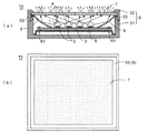
10 照明装置
2 LED(固体発光素子)
4 波長変換部材
40 頂点部
41 凹部
42 薄肉部材
43 透明な樹脂
Claims (6)
- 固体発光素子と、
前記固体発光素子の発光面を被覆する透明樹脂部材を構成する樹脂材料中に、蛍光体を含有して成る波長変換部材と、を備え、
前記波長変換部材は、縦断面視において前記固体発光素子の側方方向の厚さよりも上方方向の厚さが厚く、且つ前記固体発光素子の光導出方向に頂点部を有するように形成されていることを特徴とする発光装置。 - 前記波長変換部材は、縦断面視において縦長の凸形状となるように形成されていることを特徴とする請求項1に記載の発光装置。
- 前記波長変換部材は、縦断面視において縦長の三角形状となるように形成されていることを特徴とする請求項1に記載の発光装置。
- 前記波長変換部材は、上面視において円形状となるように形成されていることを特徴とする請求項1乃至請求項3のいずれか一項に記載の発光装置。
- 前記波長変換部材は、上面視において楕円形状となるように形成されていることを特徴とする請求項1乃至請求項3のいずれか一項に記載の発光装置。
- 請求項1乃至請求項5のいずれか一項に記載の発光装置を用いた照明装置。
Priority Applications (4)
| Application Number | Priority Date | Filing Date | Title |
|---|---|---|---|
| JP2011098920A JP5899507B2 (ja) | 2011-04-27 | 2011-04-27 | 発光装置及びそれを用いた照明装置 |
| EP12164288.8A EP2518785A3 (en) | 2011-04-27 | 2012-04-16 | Light emitting device and illumination device using the same |
| CN2012101275286A CN102760819A (zh) | 2011-04-27 | 2012-04-26 | 发光装置及包括这种发光装置的照明设备 |
| US13/456,334 US8558456B2 (en) | 2011-04-27 | 2012-04-26 | Light emitting device and illumination apparatus including same |
Applications Claiming Priority (1)
| Application Number | Priority Date | Filing Date | Title |
|---|---|---|---|
| JP2011098920A JP5899507B2 (ja) | 2011-04-27 | 2011-04-27 | 発光装置及びそれを用いた照明装置 |
Publications (2)
| Publication Number | Publication Date |
|---|---|
| JP2012231036A JP2012231036A (ja) | 2012-11-22 |
| JP5899507B2 true JP5899507B2 (ja) | 2016-04-06 |
Family
ID=46045795
Family Applications (1)
| Application Number | Title | Priority Date | Filing Date |
|---|---|---|---|
| JP2011098920A Active JP5899507B2 (ja) | 2011-04-27 | 2011-04-27 | 発光装置及びそれを用いた照明装置 |
Country Status (4)
| Country | Link |
|---|---|
| US (1) | US8558456B2 (ja) |
| EP (1) | EP2518785A3 (ja) |
| JP (1) | JP5899507B2 (ja) |
| CN (1) | CN102760819A (ja) |
Families Citing this family (17)
| Publication number | Priority date | Publication date | Assignee | Title |
|---|---|---|---|---|
| JP2013004739A (ja) * | 2011-06-16 | 2013-01-07 | Panasonic Corp | 発光装置及びそれを用いた照明器具 |
| CN103375708B (zh) * | 2012-04-26 | 2015-10-28 | 展晶科技(深圳)有限公司 | 发光二极管灯源装置 |
| US8974077B2 (en) | 2012-07-30 | 2015-03-10 | Ultravision Technologies, Llc | Heat sink for LED light source |
| CN102980744B (zh) * | 2012-11-14 | 2015-02-04 | 大连工业大学 | 一种测量光导管照明系统配光曲线的方法 |
| JP6244784B2 (ja) * | 2013-09-30 | 2017-12-13 | 日亜化学工業株式会社 | 発光装置 |
| US9976707B2 (en) | 2014-01-08 | 2018-05-22 | Philips Lighting Holding B.V. | Color mixing output for high brightness LED sources |
| US10032969B2 (en) | 2014-12-26 | 2018-07-24 | Nichia Corporation | Light emitting device |
| JP6544076B2 (ja) * | 2014-12-26 | 2019-07-17 | 日亜化学工業株式会社 | 発光装置 |
| JP6925100B2 (ja) | 2015-05-21 | 2021-08-25 | 日亜化学工業株式会社 | 発光装置 |
| JP6798772B2 (ja) * | 2015-07-31 | 2020-12-09 | 株式会社小糸製作所 | 照明装置 |
| JP6759556B2 (ja) | 2015-10-30 | 2020-09-23 | 日亜化学工業株式会社 | 照明装置 |
| JP7014948B2 (ja) | 2017-06-13 | 2022-02-02 | 日亜化学工業株式会社 | 発光装置の製造方法および発光装置 |
| CN110473950A (zh) * | 2019-07-26 | 2019-11-19 | 惠州市华星光电技术有限公司 | 背光模组及显示面板 |
| JP6993589B2 (ja) * | 2019-12-11 | 2022-02-04 | 日亜化学工業株式会社 | 発光装置及び発光装置を用いた面発光装置 |
| JP7425618B2 (ja) * | 2020-02-10 | 2024-01-31 | アオイ電子株式会社 | 発光装置の製造方法、および発光装置 |
| JP7470571B2 (ja) | 2020-05-28 | 2024-04-18 | スタンレー電気株式会社 | 発光装置 |
| JP7315858B2 (ja) | 2021-02-17 | 2023-07-27 | 日亜化学工業株式会社 | 発光装置 |
Family Cites Families (30)
| Publication number | Priority date | Publication date | Assignee | Title |
|---|---|---|---|---|
| JP2927202B2 (ja) * | 1995-03-29 | 1999-07-28 | 日亜化学工業株式会社 | Ledランプ |
| JPH08250772A (ja) * | 1996-02-23 | 1996-09-27 | Rohm Co Ltd | 発光ダイオード |
| JPH10288966A (ja) | 1997-04-11 | 1998-10-27 | Okaya Electric Ind Co Ltd | Led表示器及びその製造方法 |
| JPH1146013A (ja) * | 1997-07-25 | 1999-02-16 | Sharp Corp | Ledランプ |
| JP3315908B2 (ja) * | 1997-10-31 | 2002-08-19 | 株式会社東芝 | 半導体発光装置とその製造方法 |
| JP4471427B2 (ja) * | 1999-11-29 | 2010-06-02 | シャープ株式会社 | 半導体レーザ発光素子、及びそれを搭載した電子機器 |
| JP2002190622A (ja) * | 2000-12-22 | 2002-07-05 | Sanken Electric Co Ltd | 発光ダイオード用透光性蛍光カバー |
| JP4066620B2 (ja) * | 2000-07-21 | 2008-03-26 | 日亜化学工業株式会社 | 発光素子、および発光素子を配置した表示装置ならびに表示装置の製造方法 |
| TW552726B (en) * | 2001-07-26 | 2003-09-11 | Matsushita Electric Works Ltd | Light emitting device in use of LED |
| JP3905343B2 (ja) | 2001-10-09 | 2007-04-18 | シチズン電子株式会社 | 発光ダイオード |
| JP3813509B2 (ja) * | 2001-12-28 | 2006-08-23 | 株式会社東芝 | レンズ一体型発光素子及び航空障害灯 |
| EP1536487A4 (en) * | 2002-05-28 | 2008-02-06 | Matsushita Electric Works Ltd | ELECTROLUMINESCENT ELEMENT, LIGHT EMITTING DEVICE AND SURFACE EMISSION LIGHTING DEVICE USING THE SAME |
| JP2004273798A (ja) * | 2003-03-10 | 2004-09-30 | Toyoda Gosei Co Ltd | 発光デバイス |
| JP4123057B2 (ja) * | 2003-05-26 | 2008-07-23 | 松下電工株式会社 | 発光装置及びその製造方法 |
| JP2006054396A (ja) * | 2004-08-16 | 2006-02-23 | Toshiba Discrete Technology Kk | 発光装置 |
| JP2007035802A (ja) * | 2005-07-25 | 2007-02-08 | Matsushita Electric Works Ltd | 発光装置 |
| US20070102718A1 (en) * | 2005-11-07 | 2007-05-10 | Akira Takekuma | Lens in light emitting device |
| JP5357379B2 (ja) * | 2006-02-23 | 2013-12-04 | パナソニック株式会社 | 発光装置 |
| JP2007250817A (ja) | 2006-03-16 | 2007-09-27 | Stanley Electric Co Ltd | Led |
| JP2007273562A (ja) * | 2006-03-30 | 2007-10-18 | Toshiba Corp | 半導体発光装置 |
| KR100755612B1 (ko) * | 2006-09-21 | 2007-09-06 | 삼성전기주식회사 | Led 패키지 제조방법 및 백색 광원 모듈 제조방법 |
| JP5194675B2 (ja) | 2006-10-31 | 2013-05-08 | 東芝ライテック株式会社 | 発光装置 |
| US7810956B2 (en) * | 2007-08-23 | 2010-10-12 | Koninklijke Philips Electronics N.V. | Light source including reflective wavelength-converting layer |
| CN101577297A (zh) * | 2008-05-09 | 2009-11-11 | 旭丽电子(广州)有限公司 | 发光封装结构及其制造方法 |
| WO2009145259A1 (ja) * | 2008-05-30 | 2009-12-03 | 株式会社東芝 | 白色光源、バックライト、液晶表示装置および照明装置 |
| JP5243883B2 (ja) | 2008-08-06 | 2013-07-24 | パナソニック株式会社 | 発光装置および照明器具 |
| JP2010183035A (ja) | 2009-02-09 | 2010-08-19 | Toyoda Gosei Co Ltd | 発光装置 |
| TWI411142B (zh) * | 2009-06-23 | 2013-10-01 | Delta Electronics Inc | 發光裝置及其封裝方法 |
| JP5726409B2 (ja) | 2009-07-01 | 2015-06-03 | シャープ株式会社 | 発光装置および発光装置の製造方法 |
| CN101988636A (zh) * | 2009-07-31 | 2011-03-23 | 歌尔声学股份有限公司 | 一种白光led及其制备方法 |
-
2011
- 2011-04-27 JP JP2011098920A patent/JP5899507B2/ja active Active
-
2012
- 2012-04-16 EP EP12164288.8A patent/EP2518785A3/en not_active Withdrawn
- 2012-04-26 US US13/456,334 patent/US8558456B2/en not_active Expired - Fee Related
- 2012-04-26 CN CN2012101275286A patent/CN102760819A/zh active Pending
Also Published As
| Publication number | Publication date |
|---|---|
| CN102760819A (zh) | 2012-10-31 |
| JP2012231036A (ja) | 2012-11-22 |
| US20120274203A1 (en) | 2012-11-01 |
| EP2518785A2 (en) | 2012-10-31 |
| EP2518785A3 (en) | 2014-11-05 |
| US8558456B2 (en) | 2013-10-15 |
Similar Documents
| Publication | Publication Date | Title |
|---|---|---|
| JP5899507B2 (ja) | 発光装置及びそれを用いた照明装置 | |
| JP5899508B2 (ja) | 発光装置及びそれを用いた照明装置 | |
| JP5903672B2 (ja) | 発光装置及びそれを用いた照明装置 | |
| JP5515992B2 (ja) | 発光装置 | |
| JP5810301B2 (ja) | 照明装置 | |
| JP4238681B2 (ja) | 発光装置 | |
| JP2012248553A (ja) | 発光装置及びそれを用いた照明装置 | |
| JP4698412B2 (ja) | 発光装置および照明装置 | |
| JP2007266356A (ja) | 発光装置およびそれを用いた照明装置 | |
| JP2006237264A (ja) | 発光装置および照明装置 | |
| JP4986608B2 (ja) | 発光装置および照明装置 | |
| JP6233750B2 (ja) | 発光装置およびその製造方法、照明用光源、並びに照明装置 | |
| JP2017162940A (ja) | 発光装置及び照明装置 | |
| JP5796209B2 (ja) | 発光装置及びそれを用いた照明装置 | |
| JP5374332B2 (ja) | 照明装置 | |
| JP2006066657A (ja) | 発光装置および照明装置 | |
| JP2012204349A (ja) | 発光装置 | |
| JP5899476B2 (ja) | 発光装置及びそれを用いた照明装置 | |
| JP2012009696A (ja) | 発光装置およびそれを用いたled照明器具 | |
| JP6583673B2 (ja) | 発光装置、及び照明装置 | |
| JP2013149690A (ja) | 発光装置および照明装置 | |
| JP5312556B2 (ja) | 発光装置および照明装置 | |
| JP2010016108A (ja) | 発光装置 | |
| JP5085851B2 (ja) | 発光装置および照明装置 | |
| JP2017163002A (ja) | 発光装置、及び、照明装置 |
Legal Events
| Date | Code | Title | Description |
|---|---|---|---|
| A621 | Written request for application examination |
Free format text: JAPANESE INTERMEDIATE CODE: A621 Effective date: 20140325 |
|
| A977 | Report on retrieval |
Free format text: JAPANESE INTERMEDIATE CODE: A971007 Effective date: 20140924 |
|
| A131 | Notification of reasons for refusal |
Free format text: JAPANESE INTERMEDIATE CODE: A131 Effective date: 20141007 |
|
| A711 | Notification of change in applicant |
Free format text: JAPANESE INTERMEDIATE CODE: A711 Effective date: 20141008 |
|
| RD03 | Notification of appointment of power of attorney |
Free format text: JAPANESE INTERMEDIATE CODE: A7423 Effective date: 20141016 |
|
| A521 | Request for written amendment filed |
Free format text: JAPANESE INTERMEDIATE CODE: A523 Effective date: 20141205 |
|
| A131 | Notification of reasons for refusal |
Free format text: JAPANESE INTERMEDIATE CODE: A131 Effective date: 20150602 |
|
| A521 | Request for written amendment filed |
Free format text: JAPANESE INTERMEDIATE CODE: A523 Effective date: 20150803 |
|
| TRDD | Decision of grant or rejection written | ||
| A01 | Written decision to grant a patent or to grant a registration (utility model) |
Free format text: JAPANESE INTERMEDIATE CODE: A01 Effective date: 20151201 |
|
| A61 | First payment of annual fees (during grant procedure) |
Free format text: JAPANESE INTERMEDIATE CODE: A61 Effective date: 20151218 |
|
| R151 | Written notification of patent or utility model registration |
Ref document number: 5899507 Country of ref document: JP Free format text: JAPANESE INTERMEDIATE CODE: R151 |