JP4207858B2 - 半導体装置、表示装置及び電子機器 - Google Patents
半導体装置、表示装置及び電子機器 Download PDFInfo
- Publication number
- JP4207858B2 JP4207858B2 JP2004198040A JP2004198040A JP4207858B2 JP 4207858 B2 JP4207858 B2 JP 4207858B2 JP 2004198040 A JP2004198040 A JP 2004198040A JP 2004198040 A JP2004198040 A JP 2004198040A JP 4207858 B2 JP4207858 B2 JP 4207858B2
- Authority
- JP
- Japan
- Prior art keywords
- circuit
- wiring
- power supply
- protection
- protection circuit
- Prior art date
- Legal status (The legal status is an assumption and is not a legal conclusion. Google has not performed a legal analysis and makes no representation as to the accuracy of the status listed.)
- Expired - Lifetime
Links
- 239000004065 semiconductor Substances 0.000 title claims description 34
- 239000000758 substrate Substances 0.000 claims description 49
- 239000011159 matrix material Substances 0.000 description 27
- 230000003068 static effect Effects 0.000 description 16
- 230000005611 electricity Effects 0.000 description 15
- 239000004973 liquid crystal related substance Substances 0.000 description 15
- 238000010586 diagram Methods 0.000 description 14
- 101100163833 Arabidopsis thaliana ARP6 gene Proteins 0.000 description 11
- 230000000694 effects Effects 0.000 description 9
- 239000003990 capacitor Substances 0.000 description 8
- 229910021420 polycrystalline silicon Inorganic materials 0.000 description 8
- 229920005591 polysilicon Polymers 0.000 description 8
- 230000015556 catabolic process Effects 0.000 description 6
- 238000000707 layer-by-layer assembly Methods 0.000 description 6
- 239000010409 thin film Substances 0.000 description 6
- 235000012431 wafers Nutrition 0.000 description 6
- XUIMIQQOPSSXEZ-UHFFFAOYSA-N Silicon Chemical compound [Si] XUIMIQQOPSSXEZ-UHFFFAOYSA-N 0.000 description 5
- 238000004519 manufacturing process Methods 0.000 description 5
- 229910052710 silicon Inorganic materials 0.000 description 5
- 239000010703 silicon Substances 0.000 description 5
- 230000006378 damage Effects 0.000 description 3
- 230000005669 field effect Effects 0.000 description 3
- 238000000034 method Methods 0.000 description 3
- 230000001681 protective effect Effects 0.000 description 3
- 101100172705 Arabidopsis thaliana ESD4 gene Proteins 0.000 description 2
- 230000002159 abnormal effect Effects 0.000 description 2
- 230000000295 complement effect Effects 0.000 description 2
- 239000004020 conductor Substances 0.000 description 2
- 239000011521 glass Substances 0.000 description 2
- 239000004988 Nematic liquid crystal Substances 0.000 description 1
- NIXOWILDQLNWCW-UHFFFAOYSA-N acrylic acid group Chemical group C(C=C)(=O)O NIXOWILDQLNWCW-UHFFFAOYSA-N 0.000 description 1
- 230000002411 adverse Effects 0.000 description 1
- 229910021417 amorphous silicon Inorganic materials 0.000 description 1
- 230000005540 biological transmission Effects 0.000 description 1
- 238000007796 conventional method Methods 0.000 description 1
- 229910021419 crystalline silicon Inorganic materials 0.000 description 1
- 238000000151 deposition Methods 0.000 description 1
- 230000005684 electric field Effects 0.000 description 1
- 239000010408 film Substances 0.000 description 1
- 230000006698 induction Effects 0.000 description 1
- 230000007257 malfunction Effects 0.000 description 1
- 239000000463 material Substances 0.000 description 1
- 230000002093 peripheral effect Effects 0.000 description 1
- 230000010287 polarization Effects 0.000 description 1
- 230000001902 propagating effect Effects 0.000 description 1
- 230000000630 rising effect Effects 0.000 description 1
- 238000005070 sampling Methods 0.000 description 1
- 239000003566 sealing material Substances 0.000 description 1
Images


Classifications
-
- H—ELECTRICITY
- H10—SEMICONDUCTOR DEVICES; ELECTRIC SOLID-STATE DEVICES NOT OTHERWISE PROVIDED FOR
- H10D—INORGANIC ELECTRIC SEMICONDUCTOR DEVICES
- H10D89/00—Aspects of integrated devices not covered by groups H10D84/00 - H10D88/00
- H10D89/60—Integrated devices comprising arrangements for electrical or thermal protection, e.g. protection circuits against electrostatic discharge [ESD]
- H10D89/601—Integrated devices comprising arrangements for electrical or thermal protection, e.g. protection circuits against electrostatic discharge [ESD] for devices having insulated gate electrodes, e.g. for IGFETs or IGBTs
-
- H—ELECTRICITY
- H10—SEMICONDUCTOR DEVICES; ELECTRIC SOLID-STATE DEVICES NOT OTHERWISE PROVIDED FOR
- H10D—INORGANIC ELECTRIC SEMICONDUCTOR DEVICES
- H10D84/00—Integrated devices formed in or on semiconductor substrates that comprise only semiconducting layers, e.g. on Si wafers or on GaAs-on-Si wafers
-
- G—PHYSICS
- G02—OPTICS
- G02F—OPTICAL DEVICES OR ARRANGEMENTS FOR THE CONTROL OF LIGHT BY MODIFICATION OF THE OPTICAL PROPERTIES OF THE MEDIA OF THE ELEMENTS INVOLVED THEREIN; NON-LINEAR OPTICS; FREQUENCY-CHANGING OF LIGHT; OPTICAL LOGIC ELEMENTS; OPTICAL ANALOGUE/DIGITAL CONVERTERS
- G02F1/00—Devices or arrangements for the control of the intensity, colour, phase, polarisation or direction of light arriving from an independent light source, e.g. switching, gating or modulating; Non-linear optics
- G02F1/01—Devices or arrangements for the control of the intensity, colour, phase, polarisation or direction of light arriving from an independent light source, e.g. switching, gating or modulating; Non-linear optics for the control of the intensity, phase, polarisation or colour
- G02F1/13—Devices or arrangements for the control of the intensity, colour, phase, polarisation or direction of light arriving from an independent light source, e.g. switching, gating or modulating; Non-linear optics for the control of the intensity, phase, polarisation or colour based on liquid crystals, e.g. single liquid crystal display cells
- G02F1/133—Constructional arrangements; Operation of liquid crystal cells; Circuit arrangements
- G02F1/136—Liquid crystal cells structurally associated with a semi-conducting layer or substrate, e.g. cells forming part of an integrated circuit
- G02F1/1362—Active matrix addressed cells
- G02F1/136204—Arrangements to prevent high voltage or static electricity failures
-
- G—PHYSICS
- G09—EDUCATION; CRYPTOGRAPHY; DISPLAY; ADVERTISING; SEALS
- G09G—ARRANGEMENTS OR CIRCUITS FOR CONTROL OF INDICATING DEVICES USING STATIC MEANS TO PRESENT VARIABLE INFORMATION
- G09G3/00—Control arrangements or circuits, of interest only in connection with visual indicators other than cathode-ray tubes
- G09G3/20—Control arrangements or circuits, of interest only in connection with visual indicators other than cathode-ray tubes for presentation of an assembly of a number of characters, e.g. a page, by composing the assembly by combination of individual elements arranged in a matrix no fixed position being assigned to or needed to be assigned to the individual characters or partial characters
- G09G3/22—Control arrangements or circuits, of interest only in connection with visual indicators other than cathode-ray tubes for presentation of an assembly of a number of characters, e.g. a page, by composing the assembly by combination of individual elements arranged in a matrix no fixed position being assigned to or needed to be assigned to the individual characters or partial characters using controlled light sources
- G09G3/30—Control arrangements or circuits, of interest only in connection with visual indicators other than cathode-ray tubes for presentation of an assembly of a number of characters, e.g. a page, by composing the assembly by combination of individual elements arranged in a matrix no fixed position being assigned to or needed to be assigned to the individual characters or partial characters using controlled light sources using electroluminescent panels
- G09G3/32—Control arrangements or circuits, of interest only in connection with visual indicators other than cathode-ray tubes for presentation of an assembly of a number of characters, e.g. a page, by composing the assembly by combination of individual elements arranged in a matrix no fixed position being assigned to or needed to be assigned to the individual characters or partial characters using controlled light sources using electroluminescent panels semiconductive, e.g. using light-emitting diodes [LED]
- G09G3/3208—Control arrangements or circuits, of interest only in connection with visual indicators other than cathode-ray tubes for presentation of an assembly of a number of characters, e.g. a page, by composing the assembly by combination of individual elements arranged in a matrix no fixed position being assigned to or needed to be assigned to the individual characters or partial characters using controlled light sources using electroluminescent panels semiconductive, e.g. using light-emitting diodes [LED] organic, e.g. using organic light-emitting diodes [OLED]
- G09G3/3225—Control arrangements or circuits, of interest only in connection with visual indicators other than cathode-ray tubes for presentation of an assembly of a number of characters, e.g. a page, by composing the assembly by combination of individual elements arranged in a matrix no fixed position being assigned to or needed to be assigned to the individual characters or partial characters using controlled light sources using electroluminescent panels semiconductive, e.g. using light-emitting diodes [LED] organic, e.g. using organic light-emitting diodes [OLED] using an active matrix
-
- G—PHYSICS
- G09—EDUCATION; CRYPTOGRAPHY; DISPLAY; ADVERTISING; SEALS
- G09G—ARRANGEMENTS OR CIRCUITS FOR CONTROL OF INDICATING DEVICES USING STATIC MEANS TO PRESENT VARIABLE INFORMATION
- G09G3/00—Control arrangements or circuits, of interest only in connection with visual indicators other than cathode-ray tubes
- G09G3/20—Control arrangements or circuits, of interest only in connection with visual indicators other than cathode-ray tubes for presentation of an assembly of a number of characters, e.g. a page, by composing the assembly by combination of individual elements arranged in a matrix no fixed position being assigned to or needed to be assigned to the individual characters or partial characters
- G09G3/34—Control arrangements or circuits, of interest only in connection with visual indicators other than cathode-ray tubes for presentation of an assembly of a number of characters, e.g. a page, by composing the assembly by combination of individual elements arranged in a matrix no fixed position being assigned to or needed to be assigned to the individual characters or partial characters by control of light from an independent source
- G09G3/36—Control arrangements or circuits, of interest only in connection with visual indicators other than cathode-ray tubes for presentation of an assembly of a number of characters, e.g. a page, by composing the assembly by combination of individual elements arranged in a matrix no fixed position being assigned to or needed to be assigned to the individual characters or partial characters by control of light from an independent source using liquid crystals
- G09G3/3611—Control of matrices with row and column drivers
- G09G3/3648—Control of matrices with row and column drivers using an active matrix
-
- H—ELECTRICITY
- H10—SEMICONDUCTOR DEVICES; ELECTRIC SOLID-STATE DEVICES NOT OTHERWISE PROVIDED FOR
- H10D—INORGANIC ELECTRIC SEMICONDUCTOR DEVICES
- H10D86/00—Integrated devices formed in or on insulating or conducting substrates, e.g. formed in silicon-on-insulator [SOI] substrates or on stainless steel or glass substrates
- H10D86/40—Integrated devices formed in or on insulating or conducting substrates, e.g. formed in silicon-on-insulator [SOI] substrates or on stainless steel or glass substrates characterised by multiple TFTs
- H10D86/60—Integrated devices formed in or on insulating or conducting substrates, e.g. formed in silicon-on-insulator [SOI] substrates or on stainless steel or glass substrates characterised by multiple TFTs wherein the TFTs are in active matrices
-
- G—PHYSICS
- G09—EDUCATION; CRYPTOGRAPHY; DISPLAY; ADVERTISING; SEALS
- G09G—ARRANGEMENTS OR CIRCUITS FOR CONTROL OF INDICATING DEVICES USING STATIC MEANS TO PRESENT VARIABLE INFORMATION
- G09G2300/00—Aspects of the constitution of display devices
- G09G2300/04—Structural and physical details of display devices
- G09G2300/0421—Structural details of the set of electrodes
- G09G2300/043—Compensation electrodes or other additional electrodes in matrix displays related to distortions or compensation signals, e.g. for modifying TFT threshold voltage in column driver
-
- G—PHYSICS
- G09—EDUCATION; CRYPTOGRAPHY; DISPLAY; ADVERTISING; SEALS
- G09G—ARRANGEMENTS OR CIRCUITS FOR CONTROL OF INDICATING DEVICES USING STATIC MEANS TO PRESENT VARIABLE INFORMATION
- G09G2300/00—Aspects of the constitution of display devices
- G09G2300/08—Active matrix structure, i.e. with use of active elements, inclusive of non-linear two terminal elements, in the pixels together with light emitting or modulating elements
- G09G2300/0809—Several active elements per pixel in active matrix panels
- G09G2300/0819—Several active elements per pixel in active matrix panels used for counteracting undesired variations, e.g. feedback or autozeroing
-
- G—PHYSICS
- G09—EDUCATION; CRYPTOGRAPHY; DISPLAY; ADVERTISING; SEALS
- G09G—ARRANGEMENTS OR CIRCUITS FOR CONTROL OF INDICATING DEVICES USING STATIC MEANS TO PRESENT VARIABLE INFORMATION
- G09G2330/00—Aspects of power supply; Aspects of display protection and defect management
- G09G2330/04—Display protection
-
- H—ELECTRICITY
- H10—SEMICONDUCTOR DEVICES; ELECTRIC SOLID-STATE DEVICES NOT OTHERWISE PROVIDED FOR
- H10D—INORGANIC ELECTRIC SEMICONDUCTOR DEVICES
- H10D86/00—Integrated devices formed in or on insulating or conducting substrates, e.g. formed in silicon-on-insulator [SOI] substrates or on stainless steel or glass substrates
Landscapes
- Physics & Mathematics (AREA)
- Engineering & Computer Science (AREA)
- General Physics & Mathematics (AREA)
- Theoretical Computer Science (AREA)
- Computer Hardware Design (AREA)
- Crystallography & Structural Chemistry (AREA)
- Chemical & Material Sciences (AREA)
- Nonlinear Science (AREA)
- Microelectronics & Electronic Packaging (AREA)
- Mathematical Physics (AREA)
- Optics & Photonics (AREA)
- Semiconductor Integrated Circuits (AREA)
- Liquid Crystal (AREA)
- Thin Film Transistor (AREA)
- Metal-Oxide And Bipolar Metal-Oxide Semiconductor Integrated Circuits (AREA)
Description
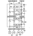
201−1〜480:走査線1〜480
202−1〜1920:データ線1〜1920
ESD1〜4:第一〜第四の保護回路
ESD11〜13:第五〜第七の保護回路
ESD21〜23:第八〜第十の保護回路
800:走査線駆動回路
801−1〜480:走査線駆動ユニット回路
Claims (6)
- 基板上に設けられた半導体回路と、
前記半導体回路に接続された配線と、
電気信号を供給するために前記配線に電気的に接続された入力端子と、
前記配線に接続されて前記半導体回路を保護する第1保護回路及び第2保護回路とを有し、
前記配線のうち、前記半導体回路と前記配線との接続部と、前記入力端子との間で、前記第1保護回路が前記配線に接続され、
前記配線のうち、前記第1保護回路と前記配線との接続部と、前記第2保護回路と前記配線との接続部との間で、前記半導体回路が前記配線に接続されている
ことを特徴とする表示装置。 - 前記配線に複数の半導体回路が接続され、
前記配線のうち前記各半導体回路の間に配置されて前記複数の半導体回路を保護する第3保護回路
を具備する請求項1の表示装置。 - 前記配線は、前記半導体回路に電源電位を供給する低電位電源配線または高電位電源配線である
請求項1または請求項2の表示装置。 - 前記配線は、前記半導体回路に信号を伝達する信号入力配線である
請求項1または請求項2の表示装置。 - 前記配線は、前記基板の周縁に沿うように当該基板の第1隅部から第2隅部にわたって形成され、
前記第1保護回路は、前記基板の前記第1隅部に配置され、
前記第2保護回路は、前記基板の前記第2隅部に配置される
請求項1から請求項4の何れかの表示装置。 - 請求項1から請求項5の何れかの表示装置を具備する電子機器。
Priority Applications (12)
| Application Number | Priority Date | Filing Date | Title |
|---|---|---|---|
| JP2004198040A JP4207858B2 (ja) | 2004-07-05 | 2004-07-05 | 半導体装置、表示装置及び電子機器 |
| CNB200510059995XA CN100476912C (zh) | 2004-07-05 | 2005-04-04 | 半导体器件、显示装置以及电子设备 |
| CN2009100043311A CN101494227B (zh) | 2004-07-05 | 2005-04-04 | 显示装置以及电子设备 |
| US11/101,450 US7755875B2 (en) | 2004-07-05 | 2005-04-08 | Semiconductor device, display device, and electronic apparatus |
| TW094111702A TW200603069A (en) | 2004-07-05 | 2005-04-13 | Semiconductor device, display device, and electronic apparatus |
| KR1020050040557A KR100760498B1 (ko) | 2004-07-05 | 2005-05-16 | 반도체 장치, 표시 장치 및 전자 기기 |
| US12/436,335 US9184157B2 (en) | 2004-07-05 | 2009-05-06 | Semiconductor device, display device, and electronic apparatus |
| US13/905,924 US8861152B2 (en) | 2004-07-05 | 2013-05-30 | Semiconductor device, display device, and electronic apparatus |
| US14/564,759 US10181462B2 (en) | 2004-07-05 | 2014-12-09 | Semiconductor device, display device, and electronic apparatus |
| US16/242,709 US10937779B2 (en) | 2004-07-05 | 2019-01-08 | Semiconductor device, display device, and electronic apparatus |
| US17/188,424 US11362081B2 (en) | 2004-07-05 | 2021-03-01 | Semiconductor device, display device, and electronic apparatus |
| US17/838,477 US11955473B2 (en) | 2004-07-05 | 2022-06-13 | Semiconductor device, display device, and electronic apparatus |
Applications Claiming Priority (1)
| Application Number | Priority Date | Filing Date | Title |
|---|---|---|---|
| JP2004198040A JP4207858B2 (ja) | 2004-07-05 | 2004-07-05 | 半導体装置、表示装置及び電子機器 |
Related Child Applications (1)
| Application Number | Title | Priority Date | Filing Date |
|---|---|---|---|
| JP2008059445A Division JP4807365B2 (ja) | 2008-03-10 | 2008-03-10 | 半導体装置、表示装置および電子機器 |
Publications (2)
| Publication Number | Publication Date |
|---|---|
| JP2006018165A JP2006018165A (ja) | 2006-01-19 |
| JP4207858B2 true JP4207858B2 (ja) | 2009-01-14 |
Family
ID=35513631
Family Applications (1)
| Application Number | Title | Priority Date | Filing Date |
|---|---|---|---|
| JP2004198040A Expired - Lifetime JP4207858B2 (ja) | 2004-07-05 | 2004-07-05 | 半導体装置、表示装置及び電子機器 |
Country Status (5)
| Country | Link |
|---|---|
| US (7) | US7755875B2 (ja) |
| JP (1) | JP4207858B2 (ja) |
| KR (1) | KR100760498B1 (ja) |
| CN (2) | CN100476912C (ja) |
| TW (1) | TW200603069A (ja) |
Families Citing this family (33)
| Publication number | Priority date | Publication date | Assignee | Title |
|---|---|---|---|---|
| KR20060134730A (ko) * | 2005-06-23 | 2006-12-28 | 삼성전자주식회사 | 어레이 기판 및 이를 구비한 표시 장치 |
| KR101404542B1 (ko) | 2006-05-25 | 2014-06-09 | 삼성디스플레이 주식회사 | 액정 표시 장치 |
| JP2008116770A (ja) * | 2006-11-07 | 2008-05-22 | Hitachi Displays Ltd | 表示装置 |
| JP2008164787A (ja) | 2006-12-27 | 2008-07-17 | Epson Imaging Devices Corp | 液晶表示装置 |
| JP2008177466A (ja) * | 2007-01-22 | 2008-07-31 | Epson Imaging Devices Corp | 表示装置およびその表示装置を備えた電子機器 |
| TWI350422B (en) * | 2007-04-25 | 2011-10-11 | Au Optronics Corp | Active device array substrate |
| KR100894254B1 (ko) * | 2007-11-06 | 2009-04-21 | 주식회사 실리콘웍스 | 전압강하가 최소화된 전원공급라인을 구비하는 반도체 칩 |
| CN101556387B (zh) * | 2008-04-11 | 2011-08-31 | 群康科技(深圳)有限公司 | 液晶显示面板 |
| KR100941835B1 (ko) | 2008-05-14 | 2010-02-11 | 삼성모바일디스플레이주식회사 | 유기전계발광표시장치 및 그의 제조방법 |
| KR101762112B1 (ko) | 2008-09-19 | 2017-07-27 | 가부시키가이샤 한도오따이 에네루기 켄큐쇼 | 액정표시장치 |
| CN102460711B (zh) * | 2009-06-09 | 2014-10-08 | 夏普株式会社 | 半导体装置 |
| JP5406295B2 (ja) * | 2009-06-18 | 2014-02-05 | シャープ株式会社 | 半導体装置 |
| KR101040859B1 (ko) | 2009-09-02 | 2011-06-14 | 삼성모바일디스플레이주식회사 | 유기전계발광 표시장치 |
| CN102576169B (zh) * | 2009-09-30 | 2014-12-03 | 夏普株式会社 | 电子装置、显示面板 |
| KR101985921B1 (ko) * | 2012-06-13 | 2019-06-05 | 삼성디스플레이 주식회사 | 유기 발광 표시 장치 |
| CN103268747B (zh) * | 2012-12-26 | 2016-01-06 | 上海中航光电子有限公司 | 一种非晶硅栅极驱动电路 |
| KR102000738B1 (ko) * | 2013-01-28 | 2019-07-23 | 삼성디스플레이 주식회사 | 정전기 방지 회로 및 이를 포함하는 표시 장치 |
| JP6107356B2 (ja) * | 2013-04-16 | 2017-04-05 | セイコーエプソン株式会社 | 静電保護回路、電気光学装置、及び電子機器 |
| JP6146165B2 (ja) | 2013-07-01 | 2017-06-14 | セイコーエプソン株式会社 | 静電気保護回路、電気光学装置、及び電子機器 |
| JP6079548B2 (ja) * | 2013-10-11 | 2017-02-15 | セイコーエプソン株式会社 | 静電気保護回路、電気光学装置、及び電子機器 |
| KR102089074B1 (ko) * | 2013-11-07 | 2020-03-13 | 엘지디스플레이 주식회사 | 표시패널용 어레이 기판 및 그 제조방법 |
| JP6360718B2 (ja) | 2014-05-16 | 2018-07-18 | 株式会社ジャパンディスプレイ | 表示装置 |
| KR102270333B1 (ko) * | 2014-11-24 | 2021-07-01 | 삼성디스플레이 주식회사 | 표시 장치 |
| WO2016105318A1 (en) | 2014-12-26 | 2016-06-30 | Gravite Mimarlik Muhendislik Tasarim San. Ve Tic. A. S. | Innovation in rapid coolers |
| CN104900206A (zh) * | 2015-06-17 | 2015-09-09 | 京东方科技集团股份有限公司 | 一种源极驱动线路板和显示装置 |
| CN104965369A (zh) * | 2015-07-28 | 2015-10-07 | 深圳市华星光电技术有限公司 | 一种阵列基板、显示面板以及显示装置 |
| US10690975B2 (en) * | 2016-03-31 | 2020-06-23 | Sharp Kabushiki Kaisha | Active matrix substrate, manufacturing method therefor and display device |
| JP6315113B2 (ja) * | 2017-01-12 | 2018-04-25 | セイコーエプソン株式会社 | 電気光学装置及び電子機器 |
| CN106847826B (zh) * | 2017-02-09 | 2021-01-15 | 京东方科技集团股份有限公司 | 一种阵列基板、显示装置以及阵列基板的制备方法 |
| CN110085585B (zh) * | 2019-05-05 | 2021-02-02 | 深圳市华星光电半导体显示技术有限公司 | 静电保护装置及显示面板 |
| US11056034B2 (en) | 2019-05-05 | 2021-07-06 | Shenzhen China Star Optoelectronics Semiconductor Display Technology Co., Ltd. | Electrostatic protection device and display panel |
| CN111399268A (zh) * | 2020-05-28 | 2020-07-10 | 厦门天马微电子有限公司 | 显示面板及显示装置 |
| KR20230102030A (ko) | 2021-12-29 | 2023-07-07 | 삼성디스플레이 주식회사 | 정전기 방전 회로 및 이를 포함하는 표시 장치 |
Family Cites Families (64)
| Publication number | Priority date | Publication date | Assignee | Title |
|---|---|---|---|---|
| JPS6155962A (ja) * | 1984-08-27 | 1986-03-20 | Oki Electric Ind Co Ltd | 電荷結合素子 |
| JPH02307258A (ja) | 1989-05-22 | 1990-12-20 | Matsushita Electron Corp | 半導体集積回路装置 |
| JP3141511B2 (ja) | 1992-04-28 | 2001-03-05 | セイコーエプソン株式会社 | 信号入力回路およびアクティブマトリクスパネル |
| US5233448A (en) * | 1992-05-04 | 1993-08-03 | Industrial Technology Research Institute | Method of manufacturing a liquid crystal display panel including photoconductive electrostatic protection |
| JP2884946B2 (ja) | 1992-09-30 | 1999-04-19 | 日本電気株式会社 | 半導体集積回路装置 |
| US5329185A (en) * | 1993-03-19 | 1994-07-12 | Gte Laboratories Incorporated | CMOS logic circuitry providing improved operating speed |
| KR940022124A (ko) * | 1993-03-24 | 1994-10-20 | 이헌조 | 액정표시장치 |
| JP3290772B2 (ja) * | 1993-08-18 | 2002-06-10 | 株式会社東芝 | 表示装置 |
| JP3029531B2 (ja) * | 1994-03-02 | 2000-04-04 | シャープ株式会社 | 液晶表示装置 |
| JPH0888323A (ja) * | 1994-09-19 | 1996-04-02 | Nippondenso Co Ltd | 半導体集積回路装置 |
| JP3085633B2 (ja) * | 1994-11-08 | 2000-09-11 | シャープ株式会社 | 反射型液晶表示装置 |
| JP2643904B2 (ja) * | 1995-04-20 | 1997-08-25 | 日本電気株式会社 | 静電保護素子 |
| US6613650B1 (en) * | 1995-07-31 | 2003-09-02 | Hyundai Electronics America | Active matrix ESD protection and testing scheme |
| JP4179483B2 (ja) * | 1996-02-13 | 2008-11-12 | 株式会社半導体エネルギー研究所 | 表示装置の作製方法 |
| JP3359844B2 (ja) * | 1996-07-22 | 2002-12-24 | シャープ株式会社 | マトリクス型画像表示装置 |
| JP4307574B2 (ja) * | 1996-09-03 | 2009-08-05 | 株式会社半導体エネルギー研究所 | アクティブマトリクス表示装置 |
| JP3483714B2 (ja) | 1996-09-20 | 2004-01-06 | 株式会社半導体エネルギー研究所 | アクティブマトリクス型液晶表示装置 |
| US6175394B1 (en) * | 1996-12-03 | 2001-01-16 | Chung-Cheng Wu | Capacitively coupled field effect transistors for electrostatic discharge protection in flat panel displays |
| US6025746A (en) * | 1996-12-23 | 2000-02-15 | Stmicroelectronics, Inc. | ESD protection circuits |
| KR100252308B1 (ko) * | 1997-01-10 | 2000-04-15 | 구본준, 론 위라하디락사 | 박막트랜지스터 어레이 |
| US6075686A (en) * | 1997-07-09 | 2000-06-13 | Industrial Technology Research Institute | ESD protection circuit for mixed mode integrated circuits with separated power pins |
| US6337722B1 (en) * | 1997-08-07 | 2002-01-08 | Lg.Philips Lcd Co., Ltd | Liquid crystal display panel having electrostatic discharge prevention circuitry |
| JP3395598B2 (ja) | 1997-09-25 | 2003-04-14 | セイコーエプソン株式会社 | アクティブマトリクス基板の製造方法および液晶表示パネル |
| KR100552299B1 (ko) * | 1998-09-16 | 2006-05-24 | 삼성전자주식회사 | 액정 표시 장치 및 이의 검사 방법 |
| JP4260250B2 (ja) * | 1997-09-25 | 2009-04-30 | 三星電子株式会社 | 静電気保護回路を有する液晶表示装置及びこの回路を利用した表示検査方法 |
| JPH11101986A (ja) * | 1997-09-26 | 1999-04-13 | Sanyo Electric Co Ltd | 表示装置及び表示装置用大基板 |
| JPH11282012A (ja) | 1998-03-30 | 1999-10-15 | Seiko Epson Corp | アクティブマトリクス基板および液晶表示装置 |
| JP3820743B2 (ja) | 1998-03-30 | 2006-09-13 | セイコーエプソン株式会社 | アクティブマトリクス基板およびアクティブマトリクス基板の製造方法および表示装置 |
| JP2000019556A (ja) | 1998-06-29 | 2000-01-21 | Hitachi Ltd | 液晶表示装置 |
| KR100307554B1 (ko) * | 1998-06-30 | 2001-11-15 | 박종섭 | Esd 소자를 구비하는 반도체장치 |
| JP2000077667A (ja) | 1998-08-28 | 2000-03-14 | Seiko Epson Corp | 半導体装置の製造方法 |
| JP4401488B2 (ja) * | 1998-09-01 | 2010-01-20 | キヤノン株式会社 | 光電変換装置 |
| US6043971A (en) * | 1998-11-04 | 2000-03-28 | L.G. Philips Lcd Co., Ltd. | Electrostatic discharge protection device for liquid crystal display using a COG package |
| JP3631384B2 (ja) | 1998-11-17 | 2005-03-23 | 富士通ディスプレイテクノロジーズ株式会社 | 液晶表示装置及び液晶表示装置の基板製造方法 |
| JP3585749B2 (ja) * | 1998-11-20 | 2004-11-04 | シャープ株式会社 | 半導体装置のシステム構成及びこの半導体装置のシステム構成を用いた液晶表示装置モジュール |
| JP3622559B2 (ja) * | 1999-02-26 | 2005-02-23 | 株式会社日立製作所 | 液晶表示装置 |
| TW498553B (en) | 1999-03-11 | 2002-08-11 | Seiko Epson Corp | Active matrix substrate, electro-optical apparatus and method for producing active matrix substrate |
| JP2001083546A (ja) * | 1999-07-12 | 2001-03-30 | Hitachi Ltd | 液晶表示装置 |
| JP3889533B2 (ja) * | 1999-09-22 | 2007-03-07 | シャープ株式会社 | 液晶表示装置及びその製造方法 |
| TW538400B (en) | 1999-11-01 | 2003-06-21 | Sharp Kk | Shift register and image display device |
| US6606080B2 (en) * | 1999-12-24 | 2003-08-12 | Semiconductor Energy Laboratory Co., Ltd. | Semiconductor display device and electronic equipment |
| TW527513B (en) * | 2000-03-06 | 2003-04-11 | Hitachi Ltd | Liquid crystal display device and manufacturing method thereof |
| JP3956572B2 (ja) | 2000-03-13 | 2007-08-08 | セイコーエプソン株式会社 | 液晶装置用基板の製造方法 |
| TW441073B (en) | 2000-03-17 | 2001-06-16 | United Microelectronics Corp | Electrostatic discharge protection circuit for integrated circuit |
| JP2001298157A (ja) | 2000-04-14 | 2001-10-26 | Nec Corp | 保護回路及びこれを搭載した半導体集積回路 |
| JP2002026333A (ja) * | 2000-07-11 | 2002-01-25 | Nec Corp | アクティブマトリクス基板の製造方法 |
| KR100658526B1 (ko) * | 2000-08-08 | 2006-12-15 | 엘지.필립스 엘시디 주식회사 | 액정 표시장치의 정전 손상 보호장치 |
| WO2002024116A1 (en) * | 2000-09-20 | 2002-03-28 | Shahinian, Lee, Jr. | Self-preserved nasal, inhalable, and topical ophthalmic preparations and medications |
| JP4718677B2 (ja) * | 2000-12-06 | 2011-07-06 | 株式会社半導体エネルギー研究所 | 半導体装置及びその作製方法 |
| GB0100733D0 (en) * | 2001-01-11 | 2001-02-21 | Koninkl Philips Electronics Nv | A method of manufacturing an active matrix substrate |
| KR100386849B1 (ko) * | 2001-07-10 | 2003-06-09 | 엘지.필립스 엘시디 주식회사 | 박막 트랜지스터 표시장치의 정전방전 방지회로 |
| GB0119299D0 (en) * | 2001-08-08 | 2001-10-03 | Koninkl Philips Electronics Nv | Electrostatic discharge protection for pixellated electronic device |
| JP2003121875A (ja) | 2001-10-09 | 2003-04-23 | Seiko Epson Corp | 素子基板装置の製造方法及び電気光学装置の製造方法並びにレチクル |
| JP3714243B2 (ja) | 2001-12-11 | 2005-11-09 | セイコーエプソン株式会社 | 半導体装置、電気光学装置、および電子機器 |
| WO2003087921A2 (en) * | 2002-04-08 | 2003-10-23 | Samsung Electronics Co., Ltd. | Liquid crystal display device |
| JP3989763B2 (ja) * | 2002-04-15 | 2007-10-10 | 株式会社半導体エネルギー研究所 | 半導体表示装置 |
| JP4200683B2 (ja) | 2002-04-16 | 2008-12-24 | セイコーエプソン株式会社 | 駆動回路、電気光学パネル、及び電子機器 |
| GB0208656D0 (en) * | 2002-04-16 | 2002-05-29 | Koninkl Philips Electronics Nv | Electroluminescent display |
| US20040027526A1 (en) * | 2002-08-08 | 2004-02-12 | Hannstar Display Corporation | Liquid crystal display device |
| TW573286B (en) * | 2002-10-31 | 2004-01-21 | Toppoly Optoelectronics Corp | Scan-driving circuit for use in planar display |
| JP3908669B2 (ja) * | 2003-01-20 | 2007-04-25 | 株式会社東芝 | 静電気放電保護回路装置 |
| TW591592B (en) * | 2003-05-09 | 2004-06-11 | Toppoly Optoelectronics Corp | Display device having electrostatic discharge protection function and panel thereof |
| JP2005049637A (ja) * | 2003-07-29 | 2005-02-24 | Seiko Epson Corp | 駆動回路及びその保護方法、電気光学装置並びに電子機器 |
| US20090149923A1 (en) * | 2007-12-07 | 2009-06-11 | 21X Corporation Dba Priavision, Inc. | Method for equi-dosed time fractionated pulsed uva irradiation of collagen/riboflavin mixtures for ocular structural augmentation |
-
2004
- 2004-07-05 JP JP2004198040A patent/JP4207858B2/ja not_active Expired - Lifetime
-
2005
- 2005-04-04 CN CNB200510059995XA patent/CN100476912C/zh active Active
- 2005-04-04 CN CN2009100043311A patent/CN101494227B/zh active Active
- 2005-04-08 US US11/101,450 patent/US7755875B2/en active Active
- 2005-04-13 TW TW094111702A patent/TW200603069A/zh unknown
- 2005-05-16 KR KR1020050040557A patent/KR100760498B1/ko active IP Right Grant
-
2009
- 2009-05-06 US US12/436,335 patent/US9184157B2/en active Active
-
2013
- 2013-05-30 US US13/905,924 patent/US8861152B2/en active Active
-
2014
- 2014-12-09 US US14/564,759 patent/US10181462B2/en active Active
-
2019
- 2019-01-08 US US16/242,709 patent/US10937779B2/en active Active
-
2021
- 2021-03-01 US US17/188,424 patent/US11362081B2/en active Active
-
2022
- 2022-06-13 US US17/838,477 patent/US11955473B2/en active Active
Also Published As
| Publication number | Publication date |
|---|---|
| US20210257352A1 (en) | 2021-08-19 |
| CN100476912C (zh) | 2009-04-08 |
| US20130250201A1 (en) | 2013-09-26 |
| US11362081B2 (en) | 2022-06-14 |
| US9184157B2 (en) | 2015-11-10 |
| US20090251834A1 (en) | 2009-10-08 |
| US10181462B2 (en) | 2019-01-15 |
| US20150091018A1 (en) | 2015-04-02 |
| US10937779B2 (en) | 2021-03-02 |
| US20190148353A1 (en) | 2019-05-16 |
| CN101494227A (zh) | 2009-07-29 |
| US20060002045A1 (en) | 2006-01-05 |
| US7755875B2 (en) | 2010-07-13 |
| US20220310588A1 (en) | 2022-09-29 |
| TW200603069A (en) | 2006-01-16 |
| US8861152B2 (en) | 2014-10-14 |
| JP2006018165A (ja) | 2006-01-19 |
| KR100760498B1 (ko) | 2007-09-20 |
| CN1722197A (zh) | 2006-01-18 |
| US11955473B2 (en) | 2024-04-09 |
| TWI312144B (ja) | 2009-07-11 |
| CN101494227B (zh) | 2012-10-17 |
| KR20060047938A (ko) | 2006-05-18 |
Similar Documents
| Publication | Publication Date | Title |
|---|---|---|
| JP4207858B2 (ja) | 半導体装置、表示装置及び電子機器 | |
| EP1898389A1 (en) | Flat panel display device | |
| KR101362015B1 (ko) | 정전기 보호회로를 구비한 평판표시장치 | |
| KR101330421B1 (ko) | 게이트 인 패널 구조의 액정표시장치 | |
| US7889189B2 (en) | Electrooptic device | |
| US9183795B2 (en) | Liquid crystal display device | |
| JP2008116770A (ja) | 表示装置 | |
| JP4807365B2 (ja) | 半導体装置、表示装置および電子機器 | |
| JPWO2007055047A1 (ja) | 表示装置およびそれを備える電子機器 | |
| US10714031B2 (en) | Display device | |
| KR20070119917A (ko) | 정전기 보호회로를 가지는 표시패널 | |
| US7280327B2 (en) | Mechanism for preventing ESD damage and LCD panel utilizing the same | |
| KR20220092098A (ko) | 표시장치 | |
| KR20070071705A (ko) | 액정표시장치 | |
| US20050195539A1 (en) | Method and device for ESD protection of a display | |
| KR100987709B1 (ko) | 액정표시장치 | |
| JP2006267545A (ja) | 電気光学装置および電子機器 | |
| KR102494157B1 (ko) | 표시장치 |
Legal Events
| Date | Code | Title | Description |
|---|---|---|---|
| A621 | Written request for application examination |
Free format text: JAPANESE INTERMEDIATE CODE: A621 Effective date: 20050204 |
|
| A977 | Report on retrieval |
Free format text: JAPANESE INTERMEDIATE CODE: A971007 Effective date: 20070222 |
|
| A131 | Notification of reasons for refusal |
Free format text: JAPANESE INTERMEDIATE CODE: A131 Effective date: 20080108 |
|
| A521 | Request for written amendment filed |
Free format text: JAPANESE INTERMEDIATE CODE: A523 Effective date: 20080310 |
|
| RD03 | Notification of appointment of power of attorney |
Free format text: JAPANESE INTERMEDIATE CODE: A7423 Effective date: 20080310 |
|
| A131 | Notification of reasons for refusal |
Free format text: JAPANESE INTERMEDIATE CODE: A131 Effective date: 20080708 |
|
| A521 | Request for written amendment filed |
Free format text: JAPANESE INTERMEDIATE CODE: A523 Effective date: 20080908 |
|
| TRDD | Decision of grant or rejection written | ||
| A01 | Written decision to grant a patent or to grant a registration (utility model) |
Free format text: JAPANESE INTERMEDIATE CODE: A01 Effective date: 20080930 |
|
| A01 | Written decision to grant a patent or to grant a registration (utility model) |
Free format text: JAPANESE INTERMEDIATE CODE: A01 |
|
| A61 | First payment of annual fees (during grant procedure) |
Free format text: JAPANESE INTERMEDIATE CODE: A61 Effective date: 20081013 |
|
| R150 | Certificate of patent or registration of utility model |
Ref document number: 4207858 Country of ref document: JP Free format text: JAPANESE INTERMEDIATE CODE: R150 Free format text: JAPANESE INTERMEDIATE CODE: R150 |
|
| FPAY | Renewal fee payment (event date is renewal date of database) |
Free format text: PAYMENT UNTIL: 20111031 Year of fee payment: 3 |
|
| FPAY | Renewal fee payment (event date is renewal date of database) |
Free format text: PAYMENT UNTIL: 20121031 Year of fee payment: 4 |
|
| FPAY | Renewal fee payment (event date is renewal date of database) |
Free format text: PAYMENT UNTIL: 20121031 Year of fee payment: 4 |
|
| FPAY | Renewal fee payment (event date is renewal date of database) |
Free format text: PAYMENT UNTIL: 20131031 Year of fee payment: 5 |
|
| S531 | Written request for registration of change of domicile |
Free format text: JAPANESE INTERMEDIATE CODE: R313531 |
|
| R350 | Written notification of registration of transfer |
Free format text: JAPANESE INTERMEDIATE CODE: R350 |
|
| R250 | Receipt of annual fees |
Free format text: JAPANESE INTERMEDIATE CODE: R250 |
|
| R250 | Receipt of annual fees |
Free format text: JAPANESE INTERMEDIATE CODE: R250 |
|
| R250 | Receipt of annual fees |
Free format text: JAPANESE INTERMEDIATE CODE: R250 |
|
| R250 | Receipt of annual fees |
Free format text: JAPANESE INTERMEDIATE CODE: R250 |
|
| R250 | Receipt of annual fees |
Free format text: JAPANESE INTERMEDIATE CODE: R250 |
|
| S111 | Request for change of ownership or part of ownership |
Free format text: JAPANESE INTERMEDIATE CODE: R313113 |
|
| R350 | Written notification of registration of transfer |
Free format text: JAPANESE INTERMEDIATE CODE: R350 |
|
| R250 | Receipt of annual fees |
Free format text: JAPANESE INTERMEDIATE CODE: R250 |
|
| EXPY | Cancellation because of completion of term |