JP2006210941A - 半導体装置 - Google Patents
半導体装置 Download PDFInfo
- Publication number
- JP2006210941A JP2006210941A JP2006085030A JP2006085030A JP2006210941A JP 2006210941 A JP2006210941 A JP 2006210941A JP 2006085030 A JP2006085030 A JP 2006085030A JP 2006085030 A JP2006085030 A JP 2006085030A JP 2006210941 A JP2006210941 A JP 2006210941A
- Authority
- JP
- Japan
- Prior art keywords
- lead
- back surface
- resin
- resin sealing
- sealing body
- Prior art date
- Legal status (The legal status is an assumption and is not a legal conclusion. Google has not performed a legal analysis and makes no representation as to the accuracy of the status listed.)
- Pending
Links
Images


Classifications
-
- H—ELECTRICITY
- H01—ELECTRIC ELEMENTS
- H01L—SEMICONDUCTOR DEVICES NOT COVERED BY CLASS H10
- H01L24/00—Arrangements for connecting or disconnecting semiconductor or solid-state bodies; Methods or apparatus related thereto
- H01L24/93—Batch processes
- H01L24/95—Batch processes at chip-level, i.e. with connecting carried out on a plurality of singulated devices, i.e. on diced chips
- H01L24/97—Batch processes at chip-level, i.e. with connecting carried out on a plurality of singulated devices, i.e. on diced chips the devices being connected to a common substrate, e.g. interposer, said common substrate being separable into individual assemblies after connecting
-
- H—ELECTRICITY
- H01—ELECTRIC ELEMENTS
- H01L—SEMICONDUCTOR DEVICES NOT COVERED BY CLASS H10
- H01L2224/00—Indexing scheme for arrangements for connecting or disconnecting semiconductor or solid-state bodies and methods related thereto as covered by H01L24/00
- H01L2224/01—Means for bonding being attached to, or being formed on, the surface to be connected, e.g. chip-to-package, die-attach, "first-level" interconnects; Manufacturing methods related thereto
- H01L2224/02—Bonding areas; Manufacturing methods related thereto
- H01L2224/04—Structure, shape, material or disposition of the bonding areas prior to the connecting process
- H01L2224/05—Structure, shape, material or disposition of the bonding areas prior to the connecting process of an individual bonding area
- H01L2224/0554—External layer
- H01L2224/0555—Shape
- H01L2224/05552—Shape in top view
- H01L2224/05554—Shape in top view being square
-
- H—ELECTRICITY
- H01—ELECTRIC ELEMENTS
- H01L—SEMICONDUCTOR DEVICES NOT COVERED BY CLASS H10
- H01L2224/00—Indexing scheme for arrangements for connecting or disconnecting semiconductor or solid-state bodies and methods related thereto as covered by H01L24/00
- H01L2224/01—Means for bonding being attached to, or being formed on, the surface to be connected, e.g. chip-to-package, die-attach, "first-level" interconnects; Manufacturing methods related thereto
- H01L2224/42—Wire connectors; Manufacturing methods related thereto
- H01L2224/44—Structure, shape, material or disposition of the wire connectors prior to the connecting process
- H01L2224/45—Structure, shape, material or disposition of the wire connectors prior to the connecting process of an individual wire connector
- H01L2224/45001—Core members of the connector
- H01L2224/45099—Material
- H01L2224/451—Material with a principal constituent of the material being a metal or a metalloid, e.g. boron (B), silicon (Si), germanium (Ge), arsenic (As), antimony (Sb), tellurium (Te) and polonium (Po), and alloys thereof
- H01L2224/45138—Material with a principal constituent of the material being a metal or a metalloid, e.g. boron (B), silicon (Si), germanium (Ge), arsenic (As), antimony (Sb), tellurium (Te) and polonium (Po), and alloys thereof the principal constituent melting at a temperature of greater than or equal to 950°C and less than 1550°C
- H01L2224/45144—Gold (Au) as principal constituent
-
- H—ELECTRICITY
- H01—ELECTRIC ELEMENTS
- H01L—SEMICONDUCTOR DEVICES NOT COVERED BY CLASS H10
- H01L2224/00—Indexing scheme for arrangements for connecting or disconnecting semiconductor or solid-state bodies and methods related thereto as covered by H01L24/00
- H01L2224/01—Means for bonding being attached to, or being formed on, the surface to be connected, e.g. chip-to-package, die-attach, "first-level" interconnects; Manufacturing methods related thereto
- H01L2224/42—Wire connectors; Manufacturing methods related thereto
- H01L2224/47—Structure, shape, material or disposition of the wire connectors after the connecting process
- H01L2224/48—Structure, shape, material or disposition of the wire connectors after the connecting process of an individual wire connector
- H01L2224/4805—Shape
- H01L2224/4809—Loop shape
- H01L2224/48091—Arched
-
- H—ELECTRICITY
- H01—ELECTRIC ELEMENTS
- H01L—SEMICONDUCTOR DEVICES NOT COVERED BY CLASS H10
- H01L2224/00—Indexing scheme for arrangements for connecting or disconnecting semiconductor or solid-state bodies and methods related thereto as covered by H01L24/00
- H01L2224/01—Means for bonding being attached to, or being formed on, the surface to be connected, e.g. chip-to-package, die-attach, "first-level" interconnects; Manufacturing methods related thereto
- H01L2224/42—Wire connectors; Manufacturing methods related thereto
- H01L2224/47—Structure, shape, material or disposition of the wire connectors after the connecting process
- H01L2224/48—Structure, shape, material or disposition of the wire connectors after the connecting process of an individual wire connector
- H01L2224/481—Disposition
- H01L2224/48151—Connecting between a semiconductor or solid-state body and an item not being a semiconductor or solid-state body, e.g. chip-to-substrate, chip-to-passive
- H01L2224/48221—Connecting between a semiconductor or solid-state body and an item not being a semiconductor or solid-state body, e.g. chip-to-substrate, chip-to-passive the body and the item being stacked
- H01L2224/48245—Connecting between a semiconductor or solid-state body and an item not being a semiconductor or solid-state body, e.g. chip-to-substrate, chip-to-passive the body and the item being stacked the item being metallic
- H01L2224/48247—Connecting between a semiconductor or solid-state body and an item not being a semiconductor or solid-state body, e.g. chip-to-substrate, chip-to-passive the body and the item being stacked the item being metallic connecting the wire to a bond pad of the item
-
- H—ELECTRICITY
- H01—ELECTRIC ELEMENTS
- H01L—SEMICONDUCTOR DEVICES NOT COVERED BY CLASS H10
- H01L2224/00—Indexing scheme for arrangements for connecting or disconnecting semiconductor or solid-state bodies and methods related thereto as covered by H01L24/00
- H01L2224/01—Means for bonding being attached to, or being formed on, the surface to be connected, e.g. chip-to-package, die-attach, "first-level" interconnects; Manufacturing methods related thereto
- H01L2224/42—Wire connectors; Manufacturing methods related thereto
- H01L2224/47—Structure, shape, material or disposition of the wire connectors after the connecting process
- H01L2224/48—Structure, shape, material or disposition of the wire connectors after the connecting process of an individual wire connector
- H01L2224/484—Connecting portions
- H01L2224/48463—Connecting portions the connecting portion on the bonding area of the semiconductor or solid-state body being a ball bond
- H01L2224/48465—Connecting portions the connecting portion on the bonding area of the semiconductor or solid-state body being a ball bond the other connecting portion not on the bonding area being a wedge bond, i.e. ball-to-wedge, regular stitch
-
- H—ELECTRICITY
- H01—ELECTRIC ELEMENTS
- H01L—SEMICONDUCTOR DEVICES NOT COVERED BY CLASS H10
- H01L2224/00—Indexing scheme for arrangements for connecting or disconnecting semiconductor or solid-state bodies and methods related thereto as covered by H01L24/00
- H01L2224/01—Means for bonding being attached to, or being formed on, the surface to be connected, e.g. chip-to-package, die-attach, "first-level" interconnects; Manufacturing methods related thereto
- H01L2224/42—Wire connectors; Manufacturing methods related thereto
- H01L2224/47—Structure, shape, material or disposition of the wire connectors after the connecting process
- H01L2224/49—Structure, shape, material or disposition of the wire connectors after the connecting process of a plurality of wire connectors
- H01L2224/491—Disposition
- H01L2224/4912—Layout
- H01L2224/49171—Fan-out arrangements
-
- H—ELECTRICITY
- H01—ELECTRIC ELEMENTS
- H01L—SEMICONDUCTOR DEVICES NOT COVERED BY CLASS H10
- H01L2924/00—Indexing scheme for arrangements or methods for connecting or disconnecting semiconductor or solid-state bodies as covered by H01L24/00
- H01L2924/01—Chemical elements
- H01L2924/01004—Beryllium [Be]
-
- H—ELECTRICITY
- H01—ELECTRIC ELEMENTS
- H01L—SEMICONDUCTOR DEVICES NOT COVERED BY CLASS H10
- H01L2924/00—Indexing scheme for arrangements or methods for connecting or disconnecting semiconductor or solid-state bodies as covered by H01L24/00
- H01L2924/01—Chemical elements
- H01L2924/01013—Aluminum [Al]
-
- H—ELECTRICITY
- H01—ELECTRIC ELEMENTS
- H01L—SEMICONDUCTOR DEVICES NOT COVERED BY CLASS H10
- H01L2924/00—Indexing scheme for arrangements or methods for connecting or disconnecting semiconductor or solid-state bodies as covered by H01L24/00
- H01L2924/01—Chemical elements
- H01L2924/01014—Silicon [Si]
-
- H—ELECTRICITY
- H01—ELECTRIC ELEMENTS
- H01L—SEMICONDUCTOR DEVICES NOT COVERED BY CLASS H10
- H01L2924/00—Indexing scheme for arrangements or methods for connecting or disconnecting semiconductor or solid-state bodies as covered by H01L24/00
- H01L2924/01—Chemical elements
- H01L2924/01019—Potassium [K]
-
- H—ELECTRICITY
- H01—ELECTRIC ELEMENTS
- H01L—SEMICONDUCTOR DEVICES NOT COVERED BY CLASS H10
- H01L2924/00—Indexing scheme for arrangements or methods for connecting or disconnecting semiconductor or solid-state bodies as covered by H01L24/00
- H01L2924/01—Chemical elements
- H01L2924/01028—Nickel [Ni]
-
- H—ELECTRICITY
- H01—ELECTRIC ELEMENTS
- H01L—SEMICONDUCTOR DEVICES NOT COVERED BY CLASS H10
- H01L2924/00—Indexing scheme for arrangements or methods for connecting or disconnecting semiconductor or solid-state bodies as covered by H01L24/00
- H01L2924/01—Chemical elements
- H01L2924/01078—Platinum [Pt]
-
- H—ELECTRICITY
- H01—ELECTRIC ELEMENTS
- H01L—SEMICONDUCTOR DEVICES NOT COVERED BY CLASS H10
- H01L2924/00—Indexing scheme for arrangements or methods for connecting or disconnecting semiconductor or solid-state bodies as covered by H01L24/00
- H01L2924/01—Chemical elements
- H01L2924/01079—Gold [Au]
-
- H—ELECTRICITY
- H01—ELECTRIC ELEMENTS
- H01L—SEMICONDUCTOR DEVICES NOT COVERED BY CLASS H10
- H01L2924/00—Indexing scheme for arrangements or methods for connecting or disconnecting semiconductor or solid-state bodies as covered by H01L24/00
- H01L2924/10—Details of semiconductor or other solid state devices to be connected
- H01L2924/11—Device type
- H01L2924/14—Integrated circuits
-
- H—ELECTRICITY
- H01—ELECTRIC ELEMENTS
- H01L—SEMICONDUCTOR DEVICES NOT COVERED BY CLASS H10
- H01L2924/00—Indexing scheme for arrangements or methods for connecting or disconnecting semiconductor or solid-state bodies as covered by H01L24/00
- H01L2924/15—Details of package parts other than the semiconductor or other solid state devices to be connected
- H01L2924/181—Encapsulation
Landscapes
- Engineering & Computer Science (AREA)
- Computer Hardware Design (AREA)
- Microelectronics & Electronic Packaging (AREA)
- Power Engineering (AREA)
- Structures Or Materials For Encapsulating Or Coating Semiconductor Devices Or Solid State Devices (AREA)
- Lead Frames For Integrated Circuits (AREA)
Abstract
【解決手段】タイバー15と、前記タイバーと一体に形成された第1及び第2リード13a、13bとを有するリードフレームを準備すると共に、キャビティを有する第1型と、キャビティを有しない第2型とからなる成形型を準備する工程と、前記タイバー、前記第1及び第2リードの夫々とを第2型である成形型の間に樹脂シートが位置するように押さえて、前記リードフレームを位置決めし、前記キャビティの内部に樹脂を注入して樹脂封止体を形成する工程とを含む半導体装置の製造方法であって、前記樹脂封止体を形成する工程において、前記第1リードと前記第2リードとの間における前記タイバーの裏面の幅15YWは、前記第1リードと前記第2リードとの間における前記タイバーの主面の幅よりも狭くなっている。
【選択図】図11
Description
(1)QFN型半導体装置は、実装基板に実装され、この実装基板と共に例えば携帯電話、携帯型情報処理端末機器、携帯型パーソナルコンピュータ等の小型電子機器に組み込まれる。QFN型半導体装置の実装は、一般的にリフローソルダリング(Reflow Soldering)法によって行われる。リフローソルダリング法とは、実装基板の電極上にスクリーン印刷等によって予め施された半田ペースト材を溶融して面実装型電子部品等を半田付けする方法である。
図39は、図37及び図38の樹脂封止工程において、成型金型にリードフレームを位置決めした状態を示す模式的平面図、
図40は、図39のM−M線に沿う模式的断面図である。なお、図37はリードフレームのリードの部分で切った断面図であり、図38はリードフレームのリード間の部分で切った断面図である。
図37乃至図40において、60は成形金型、61は上型、62は下型、63はキャビティ、64はフレーム本体、65は電極部材として使用される電極部分65aと樹脂封止工程後の切断工程において除去される除去部分65bとを有するリード、66はリード65が一体化されたタイバー、67はダイパッド、68は半導体チップ、69はボンディングワイヤ、70は樹脂シート、71はしわである。
(2)QFN型半導体装置においても、樹脂封止体に反りが発生する場合がある。樹脂封止体の裏面が凸面となる方向に反りが発生した場合、実装基板にQFN型半導体装置を実装する時、樹脂封止体の周辺部よりも中央部のスタンドオフが狭くなる。樹脂封止体の裏面から電極部材の裏面が突出する突出高さよりも大きい反りが樹脂封止体に発生した場合、実装基板の電極とQFN型半導体装置の電極部材との半田付けが困難になるため、実装不良を招く要因となる。
(1)互いに反対側の主面及び裏面と、タイバーと、前記タイバーと一体に形成された第1リードと、前記第1リードと間隔をおいて前記タイバーと一体に形成された第2リードとを有するリードフレームを準備すると共に、第1合わせ面及び前記第1合わせ面に連なるキャビティを有する第1型と、前記第1合わせ面と向かい合う第2合わせ面を有する第2型とを有する成形型を準備する工程と、
前記キャビティから前記第1合わせ面に亘って前記第1及び第2リードが位置し、かつ前記タイバー、前記第1及び第2リードの夫々の裏面と前記第2合わせ面との間に樹脂シートが位置するように、前記タイバー、前記第1及び第2リード、並びに前記樹脂シートを前記第1合わせ面と前記第2合わせ面とで夫々の方向から押さえて、前記第1型と前記第2型との間に前記リードフレームを位置決めし、その後、前記キャビティの内部に樹脂を注入して樹脂封止体を形成する工程とを含む半導体装置の製造方法であって、
前記樹脂封止体を形成する工程において、前記第1リードと前記第2リードとの間における前記タイバーの裏面の幅は、前記第1リードと前記第2リードとの間における前記タイバーの主面の幅よりも狭くなっている。
前記タイバーの主面及び裏面は、前記第1リードと前記第2リードとの間において、互いに反対側の第1辺及び第2辺を夫々有し、
前記樹脂封止体を形成する工程において、前記タイバーの裏面の第1辺及び第2辺のうちの前記リード側に位置する第1辺は、前記タイバーの主面の第1辺及び第2辺のうちの前記リード側に位置する第1辺よりも前記リードの先端からの距離が遠い位置に配置されている。
前記キャビティから前記第1合わせ面に亘って前記第1及び第2リードが位置し、かつ前記タイバー、前記第1及び第2リードの夫々の裏面と前記第2合わせ面との間に樹脂シートが位置するように、前記タイバー、前記第1及び第2リード、並びに前記樹脂シートを前記第1合わせ面と前記第2合わせ面とで夫々の方向から押さえて、前記第1型と前記第2型との間に前記リードフレームを位置決めし、その後、前記キャビティの内部に樹脂を注入して樹脂封止体を形成する工程とを含む半導体装置の製造方法であって、
前記第1及び第2リードは、前記キャビティから前記第1合わせ面に亘って延在し、かつ電極部材として使用される第1部分と、前記第1部分及び前記タイバーに連なり、かつ切断工程において切断除去される第2部分とを有し、
前記樹脂封止体を形成する工程において、前記第1及び第2リードのうちの少なくとも何れか一方のリードの第2部分における裏面の幅は、前記一方のリードの第2部分における主面の幅よりも狭くなっている。
互いに反対側の主面及び裏面を有する電極部材と、
前記半導体チップの電気と前記電極部材の主面とを電気的に接続する接続手段と、
互いに反対側の主面及び裏面を有し、前記半導体チップ、前記電極部材及び前記接続手段を封止する樹脂封止体と、
前記樹脂封止体の裏面から前記樹脂封止体の主面側に向かって窪む凹部とを有し、
前記電極部材の裏面は、前記樹脂封止体の裏面から突出し、
前記凹部の底面から前記電極部材の裏面までの段差は、前記樹脂封止体の裏面から前記電極部材の裏面までの段差よりも大きい。
前記キャビティから前記第1合わせ面に亘って前記リードが位置し、かつ前記タイバー及び前記リードと前記第2合わせ面との間に樹脂シートが位置するように、前記タイバー、前記リード及び前記樹脂シートを前記第1合わせ面と前記第2合わせ面とで夫々の方向から押さえて、前記樹脂シートに前記リードを食い込ませた状態で、前記第1型と前記第2型との間に前記リードフレームを位置決めし、その後、前記キャビティの内部に樹脂を注入して樹脂封止体を形成する工程とを含む。
本実施形態ではQFN型半導体装置に本発明を適用した例について説明する。
図2は図1に示す半導体装置の模式的底面図、
図3は図1に示す半導体装置の樹脂封止体の上部を除去した状態を示す模式的平面図、
図4は図3のA−A線に沿う模式的断面図、
図5は図4の一部を拡大した模式的断面図、
図6は図3のB−B線に沿う模式的断面図、
図7は図6の一部を拡大した模式的断面図である。
図8はリードフレームの一部を示す模式的平面図、
図9は図8の一部を拡大した模式的平面図、
図10は図9の一部を拡大した模式的平面図、
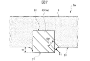
図11は図10の模式的底面図、
図12は、図10の各切断線に沿う模式的断面図であり、(a)はC−C線に沿う模式的断面図、(b)はD−D線に沿う模式的断面図、(c)はE−E線に沿う模式的断面図である。
図14は、チップボンディング工程及びワイヤボンディング工程が施された状態を示す模式的断面図、
図15は、樹脂封止工程において、成形金型にリードフレームを位置決めした状態を示す模式的断面図、
図16は、樹脂封止工程において、成型金型にリードフレームを位置決めした状態を示す模式的平面図、
図17は、図16のF−F線に沿う模式的断面図、
図18は、図16のG−G線に沿う模式的断面図、
図19は、樹脂封止工程が施された状態を示す模式的断面図、
図20は、樹脂封止工程後の切断工程を説明するための模式的断面図である。
また、リードフレーム10の位置決めは、キャビティ23の内部に、半導体チップ2、ボンディングワイヤ4、リード13、ダイパッド16及び吊りリード17等が位置する状態で行われる。
また、リードフレーム10の位置決めは、キャビティ23から上型21の合わせ面21aに亘ってリード13の電極部分13aが位置し、リード13の電極部分13aの一部及び除去部分13b、並びにタイバー15が上型21の合わせ面21aと下型22の合わせ面22aとの間に位置する状態で行われる。
また、リードフレーム10の位置決めは、リード13の電極部分13aの一部及び除去部分13b、タイバー15、並びに、これらの部分に対応する樹脂シート30の部分を上型20の合わせ面21aと下型22の合わせ面22bとで上下方向から締め付ける(押さえる)ことによって行われる。
また、リードフレーム10の位置決めは、リード13が樹脂シート30に食い込むように、上型21と下型22との締め付け力(クランプ力,挟み力)によって樹脂シート30を潰した状態で行われる。本実施形態では、リード13の食い込み量(樹脂シート30の潰れ量)は、例えば20μm程度に設定される。
また、第2リード間領域14bに発生する樹脂シート30のしわを抑制することができるため、第2リード間領域14bからリード13の電極部分13aで挟まれた第1リード間領域14aに伸びる樹脂シート30のしわを抑制することができる。
また、第2リード間領域14bに発生する樹脂シート30のしわを抑制することができるため、第2リード間領域14bからリード13の電極部分13aで挟まれた第1リード間領域14aに伸びる樹脂シート30のしわを抑制することができる。
(1)QFN型半導体装置1Aの製造における樹脂封止工程において、タイバー15のダム部(リード13間における部分)は、主面15Xの幅15XWよりも裏面15Yの幅15YWが狭くなっている(15XW>15YW)。これにより、タイバー15のダム部と樹脂シート30との接触面積が小さくなり、タイバー15のダム部によって潰される樹脂シート30の範囲が狭くなるため、タイバー15のダム部によって潰された樹脂シート30が第2リード間領域(リード13の除去部分13b間)14bに逃げる量を減らすことができる。この結果、リード13の除去部分13bで挟まれた第2リード間領域14bに発生する樹脂シート30のしわを抑制することができる。
(2)QFN型半導体装置1Aの製造における樹脂封止工程において、タイバー15のダム部は、裏面15Yのリード側に位置する辺15Y1が、主面15Xのリード側に位置する辺15X1よりも、リード13の先端部13cから、換言すればリード13の電極部分13aと除去部分13bとの間の切断ライン19から遠ざかる位置に配置されている。これにより、タイバー15のダム部によって潰される樹脂シート30の部分が第1リード間領域14aから遠ざかるため、たとえ第2リード間領域14bに樹脂シート30のしわが発生しても、第1リード間領域14aに伸びる樹脂シート30のしわを抑制することができる。
(3)QFN型半導体装置1Aの製造における樹脂封止工程において、リード13の除去部分13bの一部分は、一主面13Xの幅13XWよりも裏面13Yの幅13YWの方が狭くなっている。これにより、リード13の除去部分13bと樹脂シート30との接触面積が狭くなり、リード13の除去部分13bによって潰される樹脂シート30の範囲が狭くなるため、リード13の除去部分13bで潰された樹脂シート30が第2リード間領域14bに逃げる量を減らすことができる。この結果、リード13の除去部分13bで挟まれた第2リード間領域14bに発生する樹脂シート30のしわを抑制することができる。
(4)QFN型半導体装置1Aの製造における樹脂封止工程において、厚さが40μm程度の薄い樹脂シート30を使用し、この樹脂シート30にリード13を20μm程度食い込ませても、第1リード間領域14aに樹脂シート30のしわを発生させることなく、樹脂封止体5を形成することができるため、厚い樹脂シートを使用した場合と比較して、電極部材3の突出高さSHが高い20μm以上のQFN型半導体装置を低コストで提供することができる。
(5)実装基板50の実装面上にQFN型半導体装置1Aをリフローソルダリング法で半田付け実装する際、実装基板50の電極51とQFN型半導体装置1Aの電極部材3との間に介在された半田ペースト材52はQFN型半導体装置1Aの自重や搭載機による圧着等によって押し潰され、一部がQFP型半導体装置1Aの電極部材3間(実装基板50の電極51間)に食み(はみ)出るが、QFN型半導体装置1Aは電極部材3の突出高さSHが高い20μm程度のスタンドオフ・パッケージ構造になっていることから、食み出たペースト材52を電極部材3の側面部に溜め込むマージンが大きいため、食み出た半田ペースト材52の広がりを抑制することができる。この結果、半田ブリッジや、半田ボール等導電性異物の発生を抑制できるため、QFN型半導体装置1Aの実装不良を低減することができる。
(6)QFN型半導体装置1Aにおいて、樹脂封止体5の裏面5Yは、電極部材3に向かうに従って途中から徐々に電極部材3の裏面3Yの縁に近づくようにその高さを変える変化面5Y1となっていることから、この変化面5Y1に沿って半田ペースト材52が食み出るため、食み出た半田ペースト材52と樹脂封止体5との間に空気の巻き込みによって発生するボイドを抑制することができる。また、半田ペースト材52をスムーズに潰すことができるため、安定したペースト形状にすることができる。
図24は本発明の実施形態2である半導体装置の樹脂封止体の上部を除去した状態の模式的平面図、
図25は図24のH−H線に沿う模式的断面図、
図26は図25の一部を拡大した模式的断面図である。
図27は、本発明の実施形態3であるQFN型半導体装置の樹脂封止体の上部を除去した状態を示す模式的平面図、
図28は、図27のI−I線に沿う模式的断面図、
図29は、図28の一部を拡大した模式的断面図、
図30は、本実施形態の半導体装置の製造に用いられるリードフレームの一部を示す模式的平面図、
図31は、図30の各切断線に沿う模式的断面図であり、(a)はJ−J線に沿う模式的断面図、(b)はK−K線に沿う模式的断面図である。
図32は、本発明の実施形態4であるQFN型半導体装置の模式的底面図、
図33は、図32のL−L線に沿う模式的断面図、
図34は、図33の一部を拡大した模式的断面図、
図35は、本実施形態の半導体装置の製造における樹脂封止工程において、成形金型にリードフレームを位置決めした状態を示す模式的断面図、
図36は、本実施形態の半導体装置を実装基板に実装した状態を示す模式的断面図である。
2…半導体チップ
2a…電極
3…電極部材(リードの第1部分)
4…ボンディングワイヤ
5…樹脂封止体
6…凹部
10…リードフレーム
11…フレーム本体
12…製品形成領域
13…リード
13a…リードの電極部分
13b…リードの除去部分
14a…第1リード間領域
14b…第2リード間領域
15…タイバー
16…ダイパッド
17…吊りリード
18…モールドライン
19…切断ライン
20…成形金型
21…上型
22…下型
21a,22a…合わせ面
23…キャビティ
24…凸部
30…樹脂シート(樹脂フィルム)
31…導電層
Claims (4)
- 一主面を有する半導体チップと、
互いに反対側の主面及び裏面を有する電極部材と、
前記半導体チップの電極と前記電極部材の主面とを電気的に接続する接続手段と、
互いに反対側の主面及び裏面を有し、前記半導体チップ、前記電極部材及び前記接続手段を封止する樹脂封止体と、
前記樹脂封止体の裏面から前記樹脂封止体の主面側に向かって窪む凹部とを有し、
前記電極部材の裏面は、前記樹脂封止体の裏面から突出し、
前記凹部の底面から前記電極部材の裏面までの段差は、前記樹脂封止体の裏面から前記電極部材の裏面までの段差よりも大きいことを特徴とする半導体装置。 - 請求項1に記載の半導体装置において、
前記樹脂封止体は、前記樹脂封止体の裏面が凸面となる方向に反っていることを特徴とする半導体装置。 - 請求項1に記載の半導体装置において、
前記半導体チップは、前記樹脂封止体の主面側に位置する主面と、前記樹脂封止体の裏面側に位置する裏面とを有し、
前記半導体チップの厚さ方向の中心は、前記樹脂封止体の厚さ方向の中心よりも前記樹脂封止体の裏面側に位置していることを特徴とする半導体装置。 - 請求項1に記載の半導体装置において、
前記半導体チップが接着固定されたダイパッドを更に有し、
前記ダイパッドは、前記凹部の底面から露出していることを特徴とする半導体装置。
Priority Applications (1)
| Application Number | Priority Date | Filing Date | Title |
|---|---|---|---|
| JP2006085030A JP2006210941A (ja) | 2006-03-27 | 2006-03-27 | 半導体装置 |
Applications Claiming Priority (1)
| Application Number | Priority Date | Filing Date | Title |
|---|---|---|---|
| JP2006085030A JP2006210941A (ja) | 2006-03-27 | 2006-03-27 | 半導体装置 |
Related Parent Applications (1)
| Application Number | Title | Priority Date | Filing Date |
|---|---|---|---|
| JP2001360534A Division JP3798303B2 (ja) | 2001-11-27 | 2001-11-27 | 半導体装置及びその製造方法 |
Publications (1)
| Publication Number | Publication Date |
|---|---|
| JP2006210941A true JP2006210941A (ja) | 2006-08-10 |
Family
ID=36967343
Family Applications (1)
| Application Number | Title | Priority Date | Filing Date |
|---|---|---|---|
| JP2006085030A Pending JP2006210941A (ja) | 2006-03-27 | 2006-03-27 | 半導体装置 |
Country Status (1)
| Country | Link |
|---|---|
| JP (1) | JP2006210941A (ja) |
Cited By (4)
| Publication number | Priority date | Publication date | Assignee | Title |
|---|---|---|---|---|
| JP2016105524A (ja) * | 2016-03-10 | 2016-06-09 | 大日本印刷株式会社 | リードフレームおよびリードフレームの製造方法 |
| JP2017085049A (ja) * | 2015-10-30 | 2017-05-18 | 新光電気工業株式会社 | 半導体装置及びその製造方法、リードフレーム及びその製造方法 |
| JP2017123479A (ja) * | 2017-03-07 | 2017-07-13 | 大日本印刷株式会社 | リードフレームおよびリードフレームの製造方法 |
| WO2022153501A1 (ja) * | 2021-01-15 | 2022-07-21 | 三菱電機株式会社 | 半導体装置とその製造方法、および半導体パッケージ |
Citations (7)
| Publication number | Priority date | Publication date | Assignee | Title |
|---|---|---|---|---|
| JPH0369248U (ja) * | 1989-11-10 | 1991-07-09 | ||
| JPH0778921A (ja) * | 1993-09-09 | 1995-03-20 | Shinko Electric Ind Co Ltd | 半導体装置 |
| JPH113953A (ja) * | 1997-06-10 | 1999-01-06 | Fujitsu Ltd | 半導体装置の製造方法及び半導体装置 |
| JP2000150723A (ja) * | 1998-11-16 | 2000-05-30 | Hitachi Ltd | 半導体装置およびその製造方法 |
| JP2001035961A (ja) * | 1999-07-21 | 2001-02-09 | Sony Corp | 半導体装置及びその製造方法 |
| JP2001077266A (ja) * | 1999-09-01 | 2001-03-23 | Matsushita Electronics Industry Corp | 樹脂封止型半導体装置の製造方法 |
| JP2001185567A (ja) * | 1999-12-22 | 2001-07-06 | Hitachi Ltd | 半導体装置およびその製造方法 |
-
2006
- 2006-03-27 JP JP2006085030A patent/JP2006210941A/ja active Pending
Patent Citations (7)
| Publication number | Priority date | Publication date | Assignee | Title |
|---|---|---|---|---|
| JPH0369248U (ja) * | 1989-11-10 | 1991-07-09 | ||
| JPH0778921A (ja) * | 1993-09-09 | 1995-03-20 | Shinko Electric Ind Co Ltd | 半導体装置 |
| JPH113953A (ja) * | 1997-06-10 | 1999-01-06 | Fujitsu Ltd | 半導体装置の製造方法及び半導体装置 |
| JP2000150723A (ja) * | 1998-11-16 | 2000-05-30 | Hitachi Ltd | 半導体装置およびその製造方法 |
| JP2001035961A (ja) * | 1999-07-21 | 2001-02-09 | Sony Corp | 半導体装置及びその製造方法 |
| JP2001077266A (ja) * | 1999-09-01 | 2001-03-23 | Matsushita Electronics Industry Corp | 樹脂封止型半導体装置の製造方法 |
| JP2001185567A (ja) * | 1999-12-22 | 2001-07-06 | Hitachi Ltd | 半導体装置およびその製造方法 |
Cited By (5)
| Publication number | Priority date | Publication date | Assignee | Title |
|---|---|---|---|---|
| JP2017085049A (ja) * | 2015-10-30 | 2017-05-18 | 新光電気工業株式会社 | 半導体装置及びその製造方法、リードフレーム及びその製造方法 |
| JP2016105524A (ja) * | 2016-03-10 | 2016-06-09 | 大日本印刷株式会社 | リードフレームおよびリードフレームの製造方法 |
| JP2017123479A (ja) * | 2017-03-07 | 2017-07-13 | 大日本印刷株式会社 | リードフレームおよびリードフレームの製造方法 |
| WO2022153501A1 (ja) * | 2021-01-15 | 2022-07-21 | 三菱電機株式会社 | 半導体装置とその製造方法、および半導体パッケージ |
| JP7617954B2 (ja) | 2021-01-15 | 2025-01-20 | 三菱電機株式会社 | 半導体装置とその製造方法、および半導体パッケージ |
Similar Documents
| Publication | Publication Date | Title |
|---|---|---|
| US7514293B2 (en) | Method of manufacturing a semiconductor device | |
| US7638879B2 (en) | Semiconductor package and fabrication method thereof | |
| JP5122835B2 (ja) | 半導体装置、リードフレームおよび半導体装置の製造方法 | |
| US9385072B2 (en) | Method of manufacturing semiconductor device and semiconductor device | |
| US8133759B2 (en) | Leadframe | |
| JP2005191240A (ja) | 半導体装置及びその製造方法 | |
| JP2014007363A (ja) | 半導体装置の製造方法および半導体装置 | |
| JP6357371B2 (ja) | リードフレーム、半導体装置及びリードフレームの製造方法 | |
| KR20000048011A (ko) | 반도체 장치 | |
| JP2000307045A (ja) | リードフレームおよびそれを用いた樹脂封止型半導体装置の製造方法 | |
| US9331041B2 (en) | Semiconductor device and semiconductor device manufacturing method | |
| JP2005244035A (ja) | 半導体装置の実装方法、並びに半導体装置 | |
| JP2006210941A (ja) | 半導体装置 | |
| CN101325191B (zh) | 芯片上具有图案的四方扁平无引脚封装方法 | |
| JP2006140208A (ja) | 樹脂封止型半導体装置及びダイパッド付きリードフレーム並びにダイパッド付きリードフレームの製造方法 | |
| JP2008071927A (ja) | 半導体装置の製造方法および半導体装置 | |
| JP3798303B2 (ja) | 半導体装置及びその製造方法 | |
| JP2006279088A (ja) | 半導体装置の製造方法 | |
| JP5569097B2 (ja) | 半導体装置及びリードフレーム | |
| JP4840305B2 (ja) | 半導体装置の製造方法 | |
| JP2001077285A (ja) | リードフレームとそれを用いた樹脂封止型半導体装置の製造方法 | |
| KR20070103591A (ko) | 리드사이에 절연물질이 개재된 반도체 패키지 및 이를구비한 반도체 장치의 제조방법 | |
| JP4695672B2 (ja) | 半導体装置 | |
| JP2002164496A (ja) | 半導体装置およびその製造方法 | |
| JP2007134585A (ja) | 半導体装置及びその製造方法 |
Legal Events
| Date | Code | Title | Description |
|---|---|---|---|
| A977 | Report on retrieval |
Free format text: JAPANESE INTERMEDIATE CODE: A971007 Effective date: 20080616 |
|
| A131 | Notification of reasons for refusal |
Free format text: JAPANESE INTERMEDIATE CODE: A131 Effective date: 20080624 |
|
| A521 | Written amendment |
Free format text: JAPANESE INTERMEDIATE CODE: A523 Effective date: 20080825 |
|
| A131 | Notification of reasons for refusal |
Free format text: JAPANESE INTERMEDIATE CODE: A131 Effective date: 20081104 |
|
| A02 | Decision of refusal |
Free format text: JAPANESE INTERMEDIATE CODE: A02 Effective date: 20090310 |