EP3075737B1 - Benzimidazolo[1,2-a]benzimidazole carrying aryl- or heteroarylnitril groups for organic light emitting diodes - Google Patents
Benzimidazolo[1,2-a]benzimidazole carrying aryl- or heteroarylnitril groups for organic light emitting diodes Download PDFInfo
- Publication number
- EP3075737B1 EP3075737B1 EP15161950.9A EP15161950A EP3075737B1 EP 3075737 B1 EP3075737 B1 EP 3075737B1 EP 15161950 A EP15161950 A EP 15161950A EP 3075737 B1 EP3075737 B1 EP 3075737B1
- Authority
- EP
- European Patent Office
- Prior art keywords
- compounds
- formula
- group
- layer
- compound
- Prior art date
- Legal status (The legal status is an assumption and is not a legal conclusion. Google has not performed a legal analysis and makes no representation as to the accuracy of the status listed.)
- Active
Links
- 0 *NC([n]1c2nc3ccccc3[n]2c2c1cccc2)=N* Chemical compound *NC([n]1c2nc3ccccc3[n]2c2c1cccc2)=N* 0.000 description 18
- SDFLTYHTFPTIGX-UHFFFAOYSA-N C[n]1c(cccc2)c2c2c1cccc2 Chemical compound C[n]1c(cccc2)c2c2c1cccc2 SDFLTYHTFPTIGX-UHFFFAOYSA-N 0.000 description 2
- UWDTYENJIOEORT-UHFFFAOYSA-N C[n]1c2nc3ccccc3[n]2c2c1cccc2 Chemical compound C[n]1c2nc3ccccc3[n]2c2c1cccc2 UWDTYENJIOEORT-UHFFFAOYSA-N 0.000 description 2
- RIHYWDOIYSYQGU-UHFFFAOYSA-N N#Cc1cc(-[n]2c3nc(cccc4)c4[n]3c3cc(I)ccc23)ccc1 Chemical compound N#Cc1cc(-[n]2c3nc(cccc4)c4[n]3c3cc(I)ccc23)ccc1 RIHYWDOIYSYQGU-UHFFFAOYSA-N 0.000 description 2
- KLACMEYLRXQSMN-UHFFFAOYSA-N c(cc1[nH]2)ccc1[n]1c2nc2c1cccc2 Chemical compound c(cc1[nH]2)ccc1[n]1c2nc2c1cccc2 KLACMEYLRXQSMN-UHFFFAOYSA-N 0.000 description 2
- VPKIVADTTRODQQ-UHFFFAOYSA-N C(C1)C=Cc(c2c3cccc2)c1[n]3-c(cc1c2ccccc22)ccc1[n]2-c1cc([Si](C(C2)=CC=CC2c2c3[s]c(cccc4)c4c3ccc2)(c2ccccc2)c2ccccc2)ccc1 Chemical compound C(C1)C=Cc(c2c3cccc2)c1[n]3-c(cc1c2ccccc22)ccc1[n]2-c1cc([Si](C(C2)=CC=CC2c2c3[s]c(cccc4)c4c3ccc2)(c2ccccc2)c2ccccc2)ccc1 VPKIVADTTRODQQ-UHFFFAOYSA-N 0.000 description 1
- NPLIJEDZUGESDD-MUADHRSZSA-N C=NCc(c(-[n]1c2nc(cccc3)c3[n]2c2c1C1C=CC=C[C@@H]21)ccc1)c1-c1ccc2[o]c(ccc(-[n]3c(cccc4)c4c4c3cccc4)c3)c3c2c1 Chemical compound C=NCc(c(-[n]1c2nc(cccc3)c3[n]2c2c1C1C=CC=C[C@@H]21)ccc1)c1-c1ccc2[o]c(ccc(-[n]3c(cccc4)c4c4c3cccc4)c3)c3c2c1 NPLIJEDZUGESDD-MUADHRSZSA-N 0.000 description 1
- WGBSRLVEOCQZST-UHFFFAOYSA-O CC(C(C#N)=C(C=C)N1C2=Nc3ccccc3[NH+]2c2c1cccc2)[n]1c2nc3ccccc3[n]2c2ccccc12 Chemical compound CC(C(C#N)=C(C=C)N1C2=Nc3ccccc3[NH+]2c2c1cccc2)[n]1c2nc3ccccc3[n]2c2ccccc12 WGBSRLVEOCQZST-UHFFFAOYSA-O 0.000 description 1
- WAAFSLSDPBHQOK-UHFFFAOYSA-N CC(C)C1=CC=CC1C Chemical compound CC(C)C1=CC=CC1C WAAFSLSDPBHQOK-UHFFFAOYSA-N 0.000 description 1
- ROFIQODOBRAUSO-UHFFFAOYSA-N CC(N(C)C=C1)N1c1c(C)ccc2c1[o]c1ccccc21 Chemical compound CC(N(C)C=C1)N1c1c(C)ccc2c1[o]c1ccccc21 ROFIQODOBRAUSO-UHFFFAOYSA-N 0.000 description 1
- ZBIKORITPGTTGI-UHFFFAOYSA-N CC(O[I](c1ccccc1)OC(C)=O)=O Chemical compound CC(O[I](c1ccccc1)OC(C)=O)=O ZBIKORITPGTTGI-UHFFFAOYSA-N 0.000 description 1
- ORWRFLSTLDPQJS-UHFFFAOYSA-N CC1C(C)=CC=C1 Chemical compound CC1C(C)=CC=C1 ORWRFLSTLDPQJS-UHFFFAOYSA-N 0.000 description 1
- HSXQTOBKWYXKMU-UHFFFAOYSA-N CCC(C)(C12)C(CC)(CC)c(cccc3)c3N1c1nc(CC)c(CC)nc1N2c1ccccc1 Chemical compound CCC(C)(C12)C(CC)(CC)c(cccc3)c3N1c1nc(CC)c(CC)nc1N2c1ccccc1 HSXQTOBKWYXKMU-UHFFFAOYSA-N 0.000 description 1
- XPBUOEXLBLYLCA-UHFFFAOYSA-N C[SiH](c(cc1)cc2c1[o]c(cc1)c2cc1-[n]1c(cccc2)c2c2c1cccc2)c(cc1)cc(c2c3)c1[o]c2ccc3-[n]1c2ccccc2c2c1cccc2 Chemical compound C[SiH](c(cc1)cc2c1[o]c(cc1)c2cc1-[n]1c(cccc2)c2c2c1cccc2)c(cc1)cc(c2c3)c1[o]c2ccc3-[n]1c2ccccc2c2c1cccc2 XPBUOEXLBLYLCA-UHFFFAOYSA-N 0.000 description 1
- HVTIOHAXYSBZLK-UHFFFAOYSA-N C[n]1c(ccc(-[n]2c3nc(cccc4)c4[n]3c3ccccc23)c2)c2c2c1cccc2 Chemical compound C[n]1c(ccc(-[n]2c3nc(cccc4)c4[n]3c3ccccc23)c2)c2c2c1cccc2 HVTIOHAXYSBZLK-UHFFFAOYSA-N 0.000 description 1
- LDTOAZMVWNUPCO-UHFFFAOYSA-N C[n]1c2nc(cccc3)c3[n]2c2cc(-[n]3c(cccc4)c4c4c3cccc4)ccc12 Chemical compound C[n]1c2nc(cccc3)c3[n]2c2cc(-[n]3c(cccc4)c4c4c3cccc4)ccc12 LDTOAZMVWNUPCO-UHFFFAOYSA-N 0.000 description 1
- MQDRPHOWOQNMJE-UHFFFAOYSA-N Cc(c(C)c1)cc2c1nc1[n]2c2ccccc2[nH]1 Chemical compound Cc(c(C)c1)cc2c1nc1[n]2c2ccccc2[nH]1 MQDRPHOWOQNMJE-UHFFFAOYSA-N 0.000 description 1
- CHLICZRVGGXEOD-UHFFFAOYSA-N Cc(cc1)ccc1OC Chemical compound Cc(cc1)ccc1OC CHLICZRVGGXEOD-UHFFFAOYSA-N 0.000 description 1
- AUHZEENZYGFFBQ-UHFFFAOYSA-N Cc1cc(C)cc(C)c1 Chemical compound Cc1cc(C)cc(C)c1 AUHZEENZYGFFBQ-UHFFFAOYSA-N 0.000 description 1
- URLKBWYHVLBVBO-UHFFFAOYSA-N Cc1ccc(C)cc1 Chemical compound Cc1ccc(C)cc1 URLKBWYHVLBVBO-UHFFFAOYSA-N 0.000 description 1
- LHHWHFDZFRUYFD-UHFFFAOYSA-N N#Cc(c(-[n]1c2nc3ccccc3[n]2c2c1cccc2)ccc1-[n]2c3nc(cccc4)c4[n]3c3ccccc23)c1-[n]1c2nc(cccc3)c3[n]2c2c1cccc2 Chemical compound N#Cc(c(-[n]1c2nc3ccccc3[n]2c2c1cccc2)ccc1-[n]2c3nc(cccc4)c4[n]3c3ccccc23)c1-[n]1c2nc(cccc3)c3[n]2c2c1cccc2 LHHWHFDZFRUYFD-UHFFFAOYSA-N 0.000 description 1
- YWTXHALVWAISPR-UHFFFAOYSA-N N#Cc(c(F)c(cc1)F)c1F Chemical compound N#Cc(c(F)c(cc1)F)c1F YWTXHALVWAISPR-UHFFFAOYSA-N 0.000 description 1
- LQPBDSQNDZYFHX-UHFFFAOYSA-N N#Cc(cccc1-[n]2c3nc(cccc4)c4[n]3c3ccccc23)c1C#N Chemical compound N#Cc(cccc1-[n]2c3nc(cccc4)c4[n]3c3ccccc23)c1C#N LQPBDSQNDZYFHX-UHFFFAOYSA-N 0.000 description 1
- WWZRHCWWNKVYIA-UHFFFAOYSA-N N#Cc(cccc1-c(cc2)cc(c3c4)c2[o]c3ccc4-[n]2c3ccccc3c3c2cccc3)c1-[n]1c2nc(cccc3)c3[n]2c2c1cccc2 Chemical compound N#Cc(cccc1-c(cc2)cc(c3c4)c2[o]c3ccc4-[n]2c3ccccc3c3c2cccc3)c1-[n]1c2nc(cccc3)c3[n]2c2c1cccc2 WWZRHCWWNKVYIA-UHFFFAOYSA-N 0.000 description 1
- DBGQFLFGWUYOOQ-UHFFFAOYSA-N N#Cc1cc(-[n]2c3nc(cccc4)c4[n]3c3c2cccc3)ccc1 Chemical compound N#Cc1cc(-[n]2c3nc(cccc4)c4[n]3c3c2cccc3)ccc1 DBGQFLFGWUYOOQ-UHFFFAOYSA-N 0.000 description 1
- WIAVVLDQXGSYMV-UHFFFAOYSA-N N#Cc1cc(-[n]2c3nc(cccc4)c4[n]3c3cc([Si+](c4ccccc4)(c4ccccc4)c4ccccc4)ccc23)ccc1 Chemical compound N#Cc1cc(-[n]2c3nc(cccc4)c4[n]3c3cc([Si+](c4ccccc4)(c4ccccc4)c4ccccc4)ccc23)ccc1 WIAVVLDQXGSYMV-UHFFFAOYSA-N 0.000 description 1
- UFHAMNUEKASFQD-UHFFFAOYSA-N N#Cc1cc(-[n]2c3nc(cccc4)c4[n]3c3ccccc23)cc(C#N)c1 Chemical compound N#Cc1cc(-[n]2c3nc(cccc4)c4[n]3c3ccccc23)cc(C#N)c1 UFHAMNUEKASFQD-UHFFFAOYSA-N 0.000 description 1
- FTKGPLRXOBGESD-UHFFFAOYSA-N N#Cc1cccc(-[n]2c3nc(cccc4)c4[n]3c3c2cccc3)c1-[n]1c2nc(cccc3)c3[n]2c2c1cccc2 Chemical compound N#Cc1cccc(-[n]2c3nc(cccc4)c4[n]3c3c2cccc3)c1-[n]1c2nc(cccc3)c3[n]2c2c1cccc2 FTKGPLRXOBGESD-UHFFFAOYSA-N 0.000 description 1
- JAQFYXLPLCLPCX-UHFFFAOYSA-N N#Cc1cccc(C#N)c1-[n]1c2nc3ccccc3[n]2c2c1cccc2 Chemical compound N#Cc1cccc(C#N)c1-[n]1c2nc3ccccc3[n]2c2c1cccc2 JAQFYXLPLCLPCX-UHFFFAOYSA-N 0.000 description 1
- QXRFMGPPJWEBIX-UHFFFAOYSA-N c(cc1)ccc1-[n](c1ccccc1c1c2)c1ccc2-c(cc1)cc(c2c3cccc2)c1[n]3-c1c2[s]c(cccc3)c3c2ccn1 Chemical compound c(cc1)ccc1-[n](c1ccccc1c1c2)c1ccc2-c(cc1)cc(c2c3cccc2)c1[n]3-c1c2[s]c(cccc3)c3c2ccn1 QXRFMGPPJWEBIX-UHFFFAOYSA-N 0.000 description 1
- LIABTNDKTKNVCF-UHFFFAOYSA-N c(cc1)ccc1-c1nc(-[n]2c3nc4ccccc4[n]3c3c2cccc3)nc(-c2ccccc2)n1 Chemical compound c(cc1)ccc1-c1nc(-[n]2c3nc4ccccc4[n]3c3c2cccc3)nc(-c2ccccc2)n1 LIABTNDKTKNVCF-UHFFFAOYSA-N 0.000 description 1
- WCXKTQVEKDHQIY-UHFFFAOYSA-N c1cc(-c2cc(-c3cnccc3)cc(-c3cccnc3)c2)cc(-c2cc(-c3cnccc3)cc(-c3cccnc3)c2)c1 Chemical compound c1cc(-c2cc(-c3cnccc3)cc(-c3cccnc3)c2)cc(-c2cc(-c3cnccc3)cc(-c3cccnc3)c2)c1 WCXKTQVEKDHQIY-UHFFFAOYSA-N 0.000 description 1
- LTEREIPNJSCEHH-UHFFFAOYSA-N c1cc(cc2)c3c4c2ccc(-c(cc2)cc(c5c6)c2[o]c5ccc6-c2c(ccc5cccc(cc6)c55)c5c6cc2)c4ccc3c1 Chemical compound c1cc(cc2)c3c4c2ccc(-c(cc2)cc(c5c6)c2[o]c5ccc6-c2c(ccc5cccc(cc6)c55)c5c6cc2)c4ccc3c1 LTEREIPNJSCEHH-UHFFFAOYSA-N 0.000 description 1
Classifications
-
- C—CHEMISTRY; METALLURGY
- C07—ORGANIC CHEMISTRY
- C07D—HETEROCYCLIC COMPOUNDS
- C07D487/00—Heterocyclic compounds containing nitrogen atoms as the only ring hetero atoms in the condensed system, not provided for by groups C07D451/00 - C07D477/00
- C07D487/02—Heterocyclic compounds containing nitrogen atoms as the only ring hetero atoms in the condensed system, not provided for by groups C07D451/00 - C07D477/00 in which the condensed system contains two hetero rings
- C07D487/04—Ortho-condensed systems
-
- C—CHEMISTRY; METALLURGY
- C09—DYES; PAINTS; POLISHES; NATURAL RESINS; ADHESIVES; COMPOSITIONS NOT OTHERWISE PROVIDED FOR; APPLICATIONS OF MATERIALS NOT OTHERWISE PROVIDED FOR
- C09K—MATERIALS FOR MISCELLANEOUS APPLICATIONS, NOT PROVIDED FOR ELSEWHERE
- C09K11/00—Luminescent, e.g. electroluminescent, chemiluminescent materials
- C09K11/06—Luminescent, e.g. electroluminescent, chemiluminescent materials containing organic luminescent materials
-
- H—ELECTRICITY
- H10—SEMICONDUCTOR DEVICES; ELECTRIC SOLID-STATE DEVICES NOT OTHERWISE PROVIDED FOR
- H10K—ORGANIC ELECTRIC SOLID-STATE DEVICES
- H10K50/00—Organic light-emitting devices
- H10K50/10—OLEDs or polymer light-emitting diodes [PLED]
- H10K50/11—OLEDs or polymer light-emitting diodes [PLED] characterised by the electroluminescent [EL] layers
-
- H—ELECTRICITY
- H10—SEMICONDUCTOR DEVICES; ELECTRIC SOLID-STATE DEVICES NOT OTHERWISE PROVIDED FOR
- H10K—ORGANIC ELECTRIC SOLID-STATE DEVICES
- H10K85/00—Organic materials used in the body or electrodes of devices covered by this subclass
- H10K85/60—Organic compounds having low molecular weight
- H10K85/649—Aromatic compounds comprising a hetero atom
- H10K85/657—Polycyclic condensed heteroaromatic hydrocarbons
- H10K85/6572—Polycyclic condensed heteroaromatic hydrocarbons comprising only nitrogen in the heteroaromatic polycondensed ring system, e.g. phenanthroline or carbazole
-
- C—CHEMISTRY; METALLURGY
- C09—DYES; PAINTS; POLISHES; NATURAL RESINS; ADHESIVES; COMPOSITIONS NOT OTHERWISE PROVIDED FOR; APPLICATIONS OF MATERIALS NOT OTHERWISE PROVIDED FOR
- C09K—MATERIALS FOR MISCELLANEOUS APPLICATIONS, NOT PROVIDED FOR ELSEWHERE
- C09K2211/00—Chemical nature of organic luminescent or tenebrescent compounds
- C09K2211/10—Non-macromolecular compounds
- C09K2211/1018—Heterocyclic compounds
- C09K2211/1025—Heterocyclic compounds characterised by ligands
- C09K2211/1029—Heterocyclic compounds characterised by ligands containing one nitrogen atom as the heteroatom
-
- C—CHEMISTRY; METALLURGY
- C09—DYES; PAINTS; POLISHES; NATURAL RESINS; ADHESIVES; COMPOSITIONS NOT OTHERWISE PROVIDED FOR; APPLICATIONS OF MATERIALS NOT OTHERWISE PROVIDED FOR
- C09K—MATERIALS FOR MISCELLANEOUS APPLICATIONS, NOT PROVIDED FOR ELSEWHERE
- C09K2211/00—Chemical nature of organic luminescent or tenebrescent compounds
- C09K2211/10—Non-macromolecular compounds
- C09K2211/1018—Heterocyclic compounds
- C09K2211/1025—Heterocyclic compounds characterised by ligands
- C09K2211/1059—Heterocyclic compounds characterised by ligands containing three nitrogen atoms as heteroatoms
-
- C—CHEMISTRY; METALLURGY
- C09—DYES; PAINTS; POLISHES; NATURAL RESINS; ADHESIVES; COMPOSITIONS NOT OTHERWISE PROVIDED FOR; APPLICATIONS OF MATERIALS NOT OTHERWISE PROVIDED FOR
- C09K—MATERIALS FOR MISCELLANEOUS APPLICATIONS, NOT PROVIDED FOR ELSEWHERE
- C09K2211/00—Chemical nature of organic luminescent or tenebrescent compounds
- C09K2211/10—Non-macromolecular compounds
- C09K2211/1018—Heterocyclic compounds
- C09K2211/1025—Heterocyclic compounds characterised by ligands
- C09K2211/1088—Heterocyclic compounds characterised by ligands containing oxygen as the only heteroatom
-
- C—CHEMISTRY; METALLURGY
- C09—DYES; PAINTS; POLISHES; NATURAL RESINS; ADHESIVES; COMPOSITIONS NOT OTHERWISE PROVIDED FOR; APPLICATIONS OF MATERIALS NOT OTHERWISE PROVIDED FOR
- C09K—MATERIALS FOR MISCELLANEOUS APPLICATIONS, NOT PROVIDED FOR ELSEWHERE
- C09K2211/00—Chemical nature of organic luminescent or tenebrescent compounds
- C09K2211/10—Non-macromolecular compounds
- C09K2211/1018—Heterocyclic compounds
- C09K2211/1025—Heterocyclic compounds characterised by ligands
- C09K2211/1092—Heterocyclic compounds characterised by ligands containing sulfur as the only heteroatom
-
- H—ELECTRICITY
- H10—SEMICONDUCTOR DEVICES; ELECTRIC SOLID-STATE DEVICES NOT OTHERWISE PROVIDED FOR
- H10K—ORGANIC ELECTRIC SOLID-STATE DEVICES
- H10K2101/00—Properties of the organic materials covered by group H10K85/00
- H10K2101/10—Triplet emission
-
- H—ELECTRICITY
- H10—SEMICONDUCTOR DEVICES; ELECTRIC SOLID-STATE DEVICES NOT OTHERWISE PROVIDED FOR
- H10K—ORGANIC ELECTRIC SOLID-STATE DEVICES
- H10K50/00—Organic light-emitting devices
- H10K50/10—OLEDs or polymer light-emitting diodes [PLED]
- H10K50/14—Carrier transporting layers
- H10K50/16—Electron transporting layers
- H10K50/165—Electron transporting layers comprising dopants
-
- H—ELECTRICITY
- H10—SEMICONDUCTOR DEVICES; ELECTRIC SOLID-STATE DEVICES NOT OTHERWISE PROVIDED FOR
- H10K—ORGANIC ELECTRIC SOLID-STATE DEVICES
- H10K50/00—Organic light-emitting devices
- H10K50/10—OLEDs or polymer light-emitting diodes [PLED]
- H10K50/18—Carrier blocking layers
-
- H—ELECTRICITY
- H10—SEMICONDUCTOR DEVICES; ELECTRIC SOLID-STATE DEVICES NOT OTHERWISE PROVIDED FOR
- H10K—ORGANIC ELECTRIC SOLID-STATE DEVICES
- H10K85/00—Organic materials used in the body or electrodes of devices covered by this subclass
- H10K85/30—Coordination compounds
- H10K85/341—Transition metal complexes, e.g. Ru(II)polypyridine complexes
- H10K85/342—Transition metal complexes, e.g. Ru(II)polypyridine complexes comprising iridium
-
- H—ELECTRICITY
- H10—SEMICONDUCTOR DEVICES; ELECTRIC SOLID-STATE DEVICES NOT OTHERWISE PROVIDED FOR
- H10K—ORGANIC ELECTRIC SOLID-STATE DEVICES
- H10K85/00—Organic materials used in the body or electrodes of devices covered by this subclass
- H10K85/40—Organosilicon compounds, e.g. TIPS pentacene
-
- H—ELECTRICITY
- H10—SEMICONDUCTOR DEVICES; ELECTRIC SOLID-STATE DEVICES NOT OTHERWISE PROVIDED FOR
- H10K—ORGANIC ELECTRIC SOLID-STATE DEVICES
- H10K85/00—Organic materials used in the body or electrodes of devices covered by this subclass
- H10K85/60—Organic compounds having low molecular weight
- H10K85/649—Aromatic compounds comprising a hetero atom
- H10K85/657—Polycyclic condensed heteroaromatic hydrocarbons
- H10K85/6574—Polycyclic condensed heteroaromatic hydrocarbons comprising only oxygen in the heteroaromatic polycondensed ring system, e.g. cumarine dyes
-
- H—ELECTRICITY
- H10—SEMICONDUCTOR DEVICES; ELECTRIC SOLID-STATE DEVICES NOT OTHERWISE PROVIDED FOR
- H10K—ORGANIC ELECTRIC SOLID-STATE DEVICES
- H10K85/00—Organic materials used in the body or electrodes of devices covered by this subclass
- H10K85/60—Organic compounds having low molecular weight
- H10K85/649—Aromatic compounds comprising a hetero atom
- H10K85/657—Polycyclic condensed heteroaromatic hydrocarbons
- H10K85/6576—Polycyclic condensed heteroaromatic hydrocarbons comprising only sulfur in the heteroaromatic polycondensed ring system, e.g. benzothiophene
-
- Y—GENERAL TAGGING OF NEW TECHNOLOGICAL DEVELOPMENTS; GENERAL TAGGING OF CROSS-SECTIONAL TECHNOLOGIES SPANNING OVER SEVERAL SECTIONS OF THE IPC; TECHNICAL SUBJECTS COVERED BY FORMER USPC CROSS-REFERENCE ART COLLECTIONS [XRACs] AND DIGESTS
- Y02—TECHNOLOGIES OR APPLICATIONS FOR MITIGATION OR ADAPTATION AGAINST CLIMATE CHANGE
- Y02E—REDUCTION OF GREENHOUSE GAS [GHG] EMISSIONS, RELATED TO ENERGY GENERATION, TRANSMISSION OR DISTRIBUTION
- Y02E10/00—Energy generation through renewable energy sources
- Y02E10/50—Photovoltaic [PV] energy
- Y02E10/549—Organic PV cells
Definitions
- the present invention relates to compounds of formula Ib and their use in electronic devices, especially electroluminescent devices.
- the compounds of formula Ib When used as charge transport material, charge blocker material and/or host material in electroluminescent devices, the compounds of formula Ib may provide improved efficiency, stability, manufacturability, or spectral characteristics of electroluminescent devices and reduced driving voltage of electroluminescent devices.
- said compounds of formula Ib show low singlet triplet splitting, which makes them useful as TADF ( Thermally Activated Delayed Fluorescence, Adv. Mater. 2014, 26, 7931-7958 ) emitter or TADF host materials in combination with fluorescent emitters.
- TADF Thermally Activated Delayed Fluorescence, Adv. Mater. 2014, 26, 7931-7958
- WO2011/160757 relates to an electronic device comprising an anode, cathode and at least one organic layer which contains a compound of formulae wherein X may be a single bond and L may be a divalent group.
- X may be a single bond
- L may be a divalent group.
- WO2012/130709 relates to 4H-Imidazo[1,2-a]imidazoles, such as , for example, (A-1), a process for their production and their use in electronic devices, especially electroluminescent devices.
- WO2014/009317 relates to compounds of formula especially compounds of formula such as, for example, and a process for their production and their use in electronic devices, especially electroluminescent devices.
- the 2,5-disubstituted benzimidazo[1,2-a]benzimidazole derivatives are suitable hole transporting materials, or host materials for phosphorescent emitters.
- WO2014/044722 relates to compounds of formula which are characterized in that they substituted by benzimidazo[1,2-a]benzimidazo-5-yl and/or benzimidazo[1,2-a]benzimidazo-2,5-ylene groups and in that at least one of the substituents B 1 , B 2 , B 3 , B 4 , B 5 , B 6 , B 7 and B 8 represents N, a process for their production and their use in electronic devices, especially electroluminescent devices.
- European patent application no. 13191100.0 relates to compounds of formula which are characterized in that they are substituted by benzimidazo[1,2-a]benzimidazo-5-yl and/or benzimidazo[1,2-a]benzimidazo-2,5-ylene groups and in that at least one of the substituents B 1 , B 2 , B 3 , B 4 , B 5 , B 6 , B 7 and B 8 represents N; a process for their production and their use in electronic devices, especially electroluminescent devices.
- European patent application no. 14162667.1 relates to compounds of the formula especially wherein X 1 is H, a group of formula X 7 and X 3 are independently of each other H, or a group of formula or wherein at least one of X 1 , X 2 and X 3 is a group of formula or comprises a group of formula
- Benzimidazo[1,2-a]benzimidazo-5-yl and benzimidazo[1,2-a]benzimidazo-2-ylsubstituted benzimidazolo[2,1-b][1,3]benzothiazole derivatives are described in PCT/EP2014/066174 .
- Azabenzimidazo[2,1-a]benzimidazoles for electronic applications are described in European patent application no. 14183598.3 .
- EP14197947.9 describes carbazol compounds carrying benzimidazolo[1,2-a]benzimidazole groups of the following structure.
- EP14193401.8 describes nitril-indolo compounds carrying benzimidazolo[1,2-a]benzimidazole groups. The following compound is described:
- EP14197952.6 describes dibenzofurane compounds carrying benzimidazolo[1,2-a]benzimidazole groups of the following structure.
- WO2013/154064 A1 discloses an organic light emitting element, which has a comopound of the following formula in the light emitting layer: wherein at least one of R 1 to R 5 represents a cyano group, at least one of R 1 to R 5 represents a 9-carbazolyl group, a 1,2,3,4-terahydro-9-carbazolyl group, a 1-indolyl group or a diarylamino group, and the rest of R 1 to R 5 represent a hydrogen atom or a substituent.
- EP 2 039 737 A2 concerns an organic electroluminescence device comprising a compound of formula (I) wherein a represents an aromatic ring which may have a substituent, m represents an integer of 2 or greater, and n represents an integer of 1 or greater.
- WO2013/154064 A1 nor EP 2 039 737 A2 disclose compounds comprising benzimidazolo[1,2-a]benzimidazole groups.
- US 2014/0001446 A1 relates to a material for organic EL devices represented by formula (I)
- the material for organic EL devices represented by formula (I) has a central skeleton to which a cyano-substituted aromatic hydrocarbon group or a cyano-substituted heterocyclic group is bonded at a specific position.
- materials showing low singlet triplet splitting which makes them useful as TADF ( Thermally Activated Delayed Fluorescence, Adv. Mater. 2014, 26, 7931-7958 ) emitter or TADF host materials in combination with fluorescent emitters.
- the materials should be suitable especially for OLEDs which comprise at least one emitter, which is preferably a phosphorescence emitter, especially at least one green emitter or at least one blue emitter. It should further be possible to provide materials showing low singlet triplet splitting, which makes them useful as TADF ( Thermally Activated Delayed Fluorescence, Adv. Mater. 2014, 26, 7931-7958 ) emitter or TADF host materials in combination with fluorescent emitters.
- TADF Thermally Activated Delayed Fluorescence, Adv. Mater. 2014, 26, 7931-7958
- the materials should be suitable for providing OLEDs which ensure good efficiencies, good operative lifetimes and a high stability to thermal stress, and a low use and operating voltage of the OLEDs.
- the compounds of the present invention are characterized by a high acceptor strength, efficient bipolar characteristics and a good suitability as TADF hosts or emitters.
- the compounds of the present invention may be used for electrophotographic photoreceptors, photoelectric converters, organic solar cells (organic photovoltaics), switching elements, such as organic transistors, for example, organic FETs and organic TFTs, organic light emitting field effect transistors (OLEFETs), image sensors, dye lasers and electroluminescent devices, such as, for example, organic light-emitting diodes (OLEDs).
- organic photoreceptors organic solar cells
- organic photovoltaics organic solar cells
- switching elements such as organic transistors, for example, organic FETs and organic TFTs, organic light emitting field effect transistors (OLEFETs), image sensors, dye lasers and electroluminescent devices, such as, for example, organic light-emitting diodes (OLEDs).
- a further subject of the present invention is directed to an electronic device, comprising a compound according to the present invention.
- the electronic device is preferably an electroluminescent device, such as an organic light-emitting diode (OLED).
- OLED organic light-emitting diode
- the compounds of formula Ib can in principal be used in any layer of an EL device, but are preferably used as host, charge transport and/or charge/exciton blocking material. Particularly, the compounds of formula Ib are used as host material for green, especially blue light emitting phosphorescent emitters. Additionally, the compounds of formula Ib are used as TADF emitter or TADF host materials in combination with at least one fluorescent emitter, especially in OLEDs emitting in the blue and green region of the electromagnetic spectrum.
- a further subject of the present invention is directed to a charge transport layer, comprising a compound of formula Ib according to the present invention.
- a further subject of the present invention is directed to an emitting layer, comprising a compound of formula Ib according to the present invention.
- a compound of formula Ib is preferably used as host material, more preferably in combination with a phosphorescent emitter.
- a further subject of the present invention is directed to a charge/exciton blocking layer, comprising a compound of formula Ib according to the present invention.
- a further subject of the present invention is directed to an OLED comprising at least one compound of formula Ib as TADF emitter or TADF host material in combination with at least one fluorescent emitter.
- halogen alkyl, alkoxy, cycloalkyl, aryl, aryloxy, aralkyl, heteroaryl, arylene, heteroarylene generally have the following meaning, if said groups are not further specified in specific embodiments mentioned below:
- Halogen is fluorine, chlorine, bromine and iodine.
- C 1 -C 25 alkyl (C 1 -C 18 alkyl) is typically linear or branched, where possible. Examples are methyl, ethyl, n-propyl, isopropyl, n-butyl, sec.-butyl, isobutyl, tert.-butyl, n-pentyl, 2-pentyl, 3-pentyl, 2,2-dimethylpropyl, 1,1,3,3-tetramethylpentyl, n-hexyl, 1-methylhexyl, 1,1,3,3,5,5-hexamethylhexyl, n-heptyl, isoheptyl, 1,1,3,3-tetramethylbutyl, 1-methylheptyl, 3-methylheptyl, n-octyl, 1,1,3,3-tetramethylbutyl and 2-ethylhexyl, n-nonyl, decyl, undecyl, dodecy
- C 1 -C 8 alkyl is typically methyl, ethyl, n-propyl, isopropyl, n-butyl, sec.-butyl, isobutyl, tert.-butyl, n-pentyl, 2-pentyl, 3-pentyl, 2,2-dimethyl-propyl, n-hexyl, n-heptyl, n-octyl, 1,1,3,3-tetramethylbutyl and 2-ethylhexyl.
- C 1 -C 4 alkyl is typically methyl, ethyl, n-propyl, isopropyl, n-butyl, sec.-butyl, isobutyl, tert.-butyl.
- C 1 -C 25 alkoxy groups are straight-chain or branched alkoxy groups, e.g. methoxy, ethoxy, n-propoxy, isopropoxy, n-butoxy, sec-butoxy, tert-butoxy, amyloxy, isoamyloxy or tert-amyloxy, heptyloxy, octyloxy, isooctyloxy, nonyloxy, decyloxy, undecyloxy, dodecyloxy, tetradecyloxy, pentadecyloxy, hexadecyloxy, heptadecyloxy and octadecyloxy.
- C 1 -C 8 alkoxy examples are methoxy, ethoxy, n-propoxy, isopropoxy, n-butoxy, sec.-butoxy, isobutoxy, tert.-butoxy, n-pentyloxy, 2-pentyloxy, 3-pentyloxy, 2,2-dimethylpropoxy, n-hexyloxy, n-heptyloxy, n-octyloxy, 1,1,3,3-tetramethylbutoxy and 2-ethylhexyloxy, preferably C 1 -C 4 alkoxy such as typically methoxy, ethoxy, n-propoxy, isopropoxy, n-butoxy, sec.-butoxy, isobutoxy, tert.-butoxy.
- cycloalkyl group is typically C 5 -C 12 cycloalkyl, such as cyclopentyl, cyclohexyl, cycloheptyl, cyclooctyl, cyclononyl, cyclodecyl, cycloundecyl, cyclododecyl, preferably cyclopentyl, cyclohexyl, cycloheptyl, or cyclooctyl, which may be unsubstituted or substituted.
- C 6 -C 24 aryl (preferably C 6 -C 18 aryl), which optionally can be substituted, is typically phenyl, 4-methylphenyl, 4-methoxyphenyl, naphthyl, especially 1-naphthyl, or 2-naphthyl, biphenylyl, ter-phenylyl, pyrenyl, 2- or 9-fluorenyl, phenanthryl, or anthryl, which may be unsubstituted or substituted.
- Phenyl, 1-naphthyl and 2-naphthyl are examples of a C 6 -C 10 aryl group.
- C 6 -C 24 aryloxy which optionally can be substituted, is typically C 6 -C 10 aryloxy, which optionally can be substituted by one, or more C 1 -C 8 alkyl and/or C 1 -C 8 alkoxy groups, such as, for example, phenoxy, 1-naphthoxy, or 2-naphthoxy.
- C 7 -C 25 aralkyl is typically benzyl, 2-benzyl-2-propyl, ⁇ -phenyl-ethyl, ⁇ , ⁇ -dimethylbenzyl, ⁇ -phenyl-butyl, ⁇ , ⁇ -dimethyl- ⁇ -phenyl-butyl, ⁇ -phenyl-dodecyl, ⁇ -phenyl-octadecyl, ⁇ -phenyl-eicosyl or ⁇ -phenyl-docosyl, preferably C 7 -C 18 aralkyl such as benzyl, 2-benzyl-2-propyl, ⁇ -phenyl-ethyl, ⁇ , ⁇ -dimethylbenzyl, ⁇ -phenyl-butyl, ⁇ , ⁇ -dimethyl- ⁇ -phenyl-butyl, ⁇ -phenyl-dodecyl or ⁇ -phenyl-octadecyl, and particularly preferred C
- C 2 -C 30 heteroaryl (preferably C 2 -C 13 heteroarylaryl) represents a ring with five to seven ring atoms or a condensed ring system, wherein nitrogen, oxygen or sulfur are the possible hetero atoms, and is typically a heterocyclic group with five to 30 atoms having at least six conjugated ⁇ -electrons such as thienyl, benzothiophenyl, dibenzothiophenyl, thianthrenyl, furyl, furfuryl, 2H-pyranyl, benzofuranyl, isobenzofuranyl, dibenzofuranyl, phenoxythienyl, pyrrolyl, imidazolyl, pyrazolyl, pyridyl, bipyridyl, triazinyl, pyrimidinyl, pyrazinyl, pyridazinyl, indolizinyl, isoindolyl, indolyl, indazolyl, pur
- a C 2 -C 13 heteroaryl group is for example, benzimidazo[1,2-a]benzimidazo-5-yl benzimidazo[1,2-a]benzimidazo-2-yl benzimidazolo[2,1-b][1,3]benzothiazolyl, benzimidazolo[2,1-b][1,3]benzoxazole, carbazolyl, dibenzofuranyl, or dibenzotihophenyl, which can be unsubstituted or substituted, especially by C 6 -C 10 aryl, or C 6 -C 10 aryl, which is substituted by C 1 -C 4 alkyl; or C 2 -C 13 heteroaryl.
- C 2 -C 30 heteroaryl (preferably C 2 -C 13 heteroarylaryl) means that the heteroaryl residue comprises at least 2 carbon atoms and at most 30 carbon atoms in the base skeleton (without substituents).
- the further atoms in the heteroaryl base skeleton are heteroatoms (N, O and/or S).
- R 24 is in each case independently C 1 -C 18 alkyl, such as methyl, ethyl, n-propyl, iso-propyl, n-butyl, isobutyl, sec-butyl, hexyl, octyl, or 2-ethyl-hexyl, or C 6 -C 14 aryl, such as phenyl, tolyl, naphthyl, phenanthronyl, triphenylenyl, fluoranthenyl or biphenylyl.
- C 1 -C 18 alkyl such as methyl, ethyl, n-propyl, iso-propyl, n-butyl, isobutyl, sec-butyl, hexyl, octyl, or 2-ethyl-hexyl
- C 6 -C 14 aryl such as phenyl, tolyl, naphthyl, phenanthro
- C 6 -C 24 arylene groups which optionally can be substituted by G, are typically phenylene, 4-methylphenylene, 4-methoxyphenylene, naphthylene, especially 1-naphthylene, or 2-naphthylene, biphenylylene, terphenylylene, pyrenylene, 2- or 9-fluorenylene, phenanthrylene, or anthrylene, which may be unsubstituted or substituted.
- Preferred C 6 -C 24 arylen groups are 1,3-phenylene, 3,3'-biphenylylene, 3,3'-m-terphenylene, 2- or 9-fluorenylene, phenanthrylene, which may be unsubstituted or substituted.
- C 2 -C 30 heteroarylene groups which optionally can be substituted by G, represent a ring with five to seven ring atoms or a condensed ring system, wherein nitrogen, oxygen or sulfur are the possible hetero atoms, and is typically a heterocyclic group with five to 30 atoms having at least six conjugated -electrons such as thienylene, benzothiophenylene, dibenzothiophenylene, thianthrenylene, furylene, furfurylene, 2H-pyranylene, benzofuranylene, isobenzofuranylene, dibenzofuranylene, phenoxythienylene, pyrrolylene, imidazolylene, pyrazolylene, pyridylene, bipyridylene, triazinylene, pyrimidinylene, pyrazinylene, pyridazinylene, indolizinylene, isoindolylene, indolylene, indazolylene, puriny
- Preferred C 2 -C 30 heteroarylen groups are pyridylene, triazinylene, pyrimidinylene, carbazolylene, dibenzofuranylene and benzimidazo[1,2-a]benzimidazo-2,5-ylene which can be unsubstituted or substituted, especially by C 6 -C 10 aryl, C 6 -d 10 aryl which is substituted by C 1 -C 4 alkyl; or C 2 -C 14 heteroaryl.
- Possible preferred substituents of the above-mentioned groups are C 1 -C 8 alkyl, a hydroxyl group, a mercapto group, C 1 -C 8 alkoxy, C 1 -C 8 alkylthio, halogen, halo-C 1 -C 8 alkyl, or a cyano group.
- the C 6 -C 24 aryl (C 6 -C 18 aryl) and C 2 -C 30 heteroaryl groups are preferably substituted by one, or more C 1 -C 8 alkyl groups.
- a substituent occurs more than one time in a group, it can be different in each occurrence.
- Halo-C 1 -C 8 alkyl is an alkyl group where at least one of the hydrogen atoms is replaced by a halogen atom. Examples are -CF 3 , -CF 2 CF 3 , -CF 2 CF 2 CF 3 , -CF(CF 3 ) 2 , -(CF 2 ) 3 CF 3 , and -C(CF 3 ) 3 .
- substituted by G means that one, or more, especially one to three substituents G might be present.
- G is preferably -OR 69 , -SR 69 , -NR 65 R 66 ; a C 1 -C 18 alkyl group, a C 6 -C 14 aryl group, a C 6 -C 14 aryl group, which is substituted by F, or C 1 -C 18 alkyl; a C 2 -C 13 heteroaryl group, or a C 2 -C 13 heteroaryl group, which is substituted by F, or C 1 -C 18 alkyl; wherein R 65 , R 66 and R 69 are independently of each other C 1 -C 18 alkyl, such as methyl, ethyl, n-propyl, iso-propyl, n-butyl, isobutyl, sec-butyl, hexyl, octyl, or 2-ethyl-hexyl, or C 6 -C 14 aryl, such as phenyl, tolyl, naphthyl,
- a is 0 or 1
- b is 0 or 1
- the sum of a + b is at least1.
- a is preferably 0.
- X 3 is a single bond.
- R 7 is H or a group of the following formula: or -SiR 70 R 71 R 72 .
- R 70 and R 71 are independently of each other a C 1 -C 18 alkyl group, a C 6 -C 18 aryl group, or a C 6 -C 18 aryl group, which is substituted by C 1 -C 18 alkyl
- R 72 is a C 1 -C 18 alkyl group, a C 6 -C 18 aryl group, or a C 6 -C 18 aryl group, which is substituted by C 1 -C 18 alkyl
- R 70 , R 71 and R 72 are phenyl.
- Suitable compounds of the invention are:
- R 7 , X 3 , X 1 , a and b are defined above and below.
- X 3 , X 1 , a and b are defined above and below.
- the compounds of formula ( Ib ) are preferably compounds of formula ( Ib' )
- a is 0 or 1 and b is 0 or 1, whereby the sum of a and b is at least 1;
- X 1 is a group of the following formula: X 3 is a single bond.
- the compounds of formula ( Ic ) are preferably compounds of formula ( Ic' )
- formula (Ib) are the following compounds, whereby the 2nd and 3rd compound in the 2nd line on page 23 are for reference only:
- aryl-nitrile or heteroaryl- nitrile benzimidazolo[1,2-a]benzimidazoles derivatives of the present invention are found to be suitable for use in organo-electroluminescent devices.
- certain aryl-nitrile or heteroaryl- nitrile benzimidazolo[1,2-a]benzimidazoles derivatives are suitable host materials, especially host materials for phosphorescent emitters, charge transport materials and/or charge/exciton blocker materials with good efficiency and durability.
- said aryl-nitrile or heteroaryl- nitrile benzimidazolo[1,2-a]benzimidazoles show low singlet triplet splitting, which makes them useful as TADF ( Thermally Activated Delayed Fluorescence, Adv. Mater. 2014, 26, 7931-7958 ) emitter or TADF host materials in combination with fluorescent emitters.
- TADF Thermally Activated Delayed Fluorescence, Adv. Mater. 2014, 26, 7931-7958
- the TADF emitter or TADF host materials can be used together with one or more additional host materials.
- the compounds of the present invention are characterized by a high acceptor strength, efficient bipolar characteristics and a good suitability as TADF hosts or emitters.
- the compounds of the present invention may be used for electrophotographic photoreceptors, photoelectric converters, organic solar cells (organic photovoltaics), switching elements, such as organic transistors, for example, organic FETs and organic TFTs, organic light emitting field effect transistors (OLEFETs), image sensors, dye lasers and electroluminescent devices (EL devices), such as, for example, organic light-emitting diodes (OLEDs).
- organic transistors for example, organic FETs and organic TFTs, organic light emitting field effect transistors (OLEFETs), image sensors, dye lasers and electroluminescent devices (EL devices), such as, for example, organic light-emitting diodes (OLEDs).
- EL devices electroluminescent devices
- the compounds of the present invention are used in electroluminescent devices, especially in OLEDs.
- a further subject of the present invention is directed to an electronic device, comprising a compound according to the present invention.
- the electronic device is preferably an electroluminescent device (EL-device), especially an OLED.
- the compounds of formula Ib can in principal be used in any layer of an EL device, but are preferably used as host, charge transport and/or charge/exciton blocking material. Particularly, the compounds of formula Ib are used as host material for green, especially blue light emitting emitters, which are preferably phosphorescent emitters.
- a further subject of the present invention is directed to a charge transport layer comprising a compound of formula Ib according to the present invention.
- a further subject of the present invention is directed to an emitting layer, comprising a compound of formula Ib according to the present invention.
- a compound of formula Ib is preferably used as host material in combination with an emitter, which is preferably a phosphorescent emitter.
- a further subject of the present invention is directed to a charge/exciton blocking layer, comprising a compound of formula Ib according to the present invention.
- Formula (I) i.a. encompasses the compounds of the invention, namely the compounds of formula (Ib).
- the introduction of the group -X 3 -X 4 -CN is generally carried out by reacting the base skeleton with a group Hal-X 3 -X 4 -CN, wherein Hal is F, Cl, Br or I, preferably F, Br or I. Suitable groups X 3 and X 4 are mentioned before.
- the nucleophilic aromatic substitution (N-arylation) of with F-X 3 -X 4 -CN is generally performed in the presence of a base ( Angew. Chem. 2012, 124, 8136 -8140 , Angew. Chem. Int. Ed. 2008, 47, 8104 -8107 ).
- Suitable bases are known to those skilled in the art and are preferably selected from the group consisting of alkali metal alkali metal and alkaline earth metal hydroxides such as NaOH, KOH, Ca(OH) 2 , alkali metal hydrides such as NaH, KH, alkali metal amides such as NaNH 2 , alkali metal or alkaline earth metal carbonates such as K 2 CO 3 or Cs 2 CO 3 , alkaline metal phosphates such as K 3 PO 4 alkaline metal fluorides such as KF, CsF and alkali metal alkoxides such as NaOMe, NaOEt.
- alkali metal alkali metal and alkaline earth metal hydroxides such as NaOH, KOH, Ca(OH) 2
- alkali metal hydrides such as NaH, KH
- alkali metal amides such as NaNH 2
- alkali metal or alkaline earth metal carbonates such as K 2 CO 3 or Cs 2 CO 3
- the nucleophilic aromatic substitution can be performed in solvent or in a melt.
- the reaction is carried out in a solvent.
- Suitable solvents are, for example, (polar) aprotic solvents such as dimethyl sulfoxide (DMSO), dimethylformamide (DMF), N-methyl-2-pyrrolidone (NMP) or dimethylacetamide (DMA).
- the reaction temperature is strongly dependent on the reactivity of the aryl fluoride.
- the reaction (N-arylation) is preferably carried out at a temperature of -10 to 220 °C, more preferably 60 to 150 °C.
- the Ullmann coupling of the compound of formula with a compound of formula Y-X 3 -X 4 -CN is done in the presence of copper, or a copper salt, such as, for example, Cul, CuBr, Cu 2 O, or CuO, and a ligand, such as, for example, L-proline, trans-cyclohexane-1,2-diamine (DACH), 1,10-phenanthroline in a solvent, such as, for example, dimethylsulfoxide (DMSO), dimethylformamide (DMF), dimethylacetamide (DMA), N-methylpyrrolidone (NMP) and dioxane, or a solvent mixture.
- the reaction temperature is dependent on the reactivity of the starting materials, but is generally in the range of 25 to 200 °C. If copper salt are used without a ligand the reaction temperatures are higher.
- N-arylation is, for example, disclosed in H. Gilman and D. A. Shirley, J. Am. Chem. Soc. 66 (1944) 888 ; D. Li et al., Dyes and Pigments 49 (2001) 181 - 186 and Eur. J. Org. Chem. (2007) 2147-2151 .
- DACH is ( ⁇ )-trans-1,2-diaminocyclohexane
- the groups Hal-X 3 -X 4 -CN are commercially available or prepared by processes known in the art. Suitable preparation processes fore some groups Hal-X 3 -X 4 -CN are mentioned in the following.
- Suitable base skeletons of the formula are either commercially available (especially in the cases when X is S, O, NH), or can be obtained by processes known to those skilled in the art. Reference is made to WO2010079051 and EP1885818 .
- halogenation of said base skeletons can be performed by methods known to those skilled in the art. Preference is given to brominating or iodinating in the 3 and 6 positions (dibromination, diiodation or mixed bromination/iodation) or in the 3 or 6 positions (monobromination, monoiodation) of the base skeleton in the case of carbazole, respectively in the 2 and 8 positions (dibromination, diiodation) or in the 2 or 8 positions (monobromination, monoiodation) of the base skeleton in the case of dibenzofuran and dibenzothiophene.
- Optionally substituted dibenzofurans, dibenzothiophenes and carbazoles can be dibrominated in the 2,8 positions (dibenzofuran and dibenzothiophene) or 3,6 positions (carbazole) with bromine or NBS in glacial acetic acid or in chloroform.
- the bromination with Br 2 can be effected in glacial acetic acid or chloroform at low temperatures, e.g. 0°C.
- Dibenzofuran (dibenzothiophene) can be monobrominated in the 3 position by a sequence known to those skilled in the art, comprising a nitration, reduction and subsequent Sandmeyer reaction.
- Cl- or F-substituted dibenzofurans, dibenzothiophenes and carbazoles are preferred.
- the chlorination is described, inter alia, in J. Heterocyclic Chemistry, 34 (1997) 891-900 , Org. Lett., 6 (2004) 3501-3504 ; J. Chem. Soc. [Section] C: Organic, 16 (1971) 2775-7 , Tetrahedron Lett. 25 (1984) 5363-6 , J. Org. Chem. 69 (2004) 8177-8182 .
- the fluorination is described in J. Org. Chem. 63 (1998) 878-880 and J. Chem. Soc., Perkin Trans. 2, 5 (2002) 953-957 .
- the introduction of the skeleton can be affected, for example, by copper-catalyzed coupling (Ullmann reaction). Suitable reaction components and reaction conditions for carrying out the Ullmann reaction are mentioned above.
- DACH is ( ⁇ )-trans-1,2-diaminocyclohexane
- the introduction of the skeleton especially in cases, wherein the skeleton is substituted, e.g. by a group or can be affected, for example, by Pd catalyzed coupling of diboronic acid or diboronate group containing dibenzofurans, dibenzothiophenes or carbazoles with halogenated aromatic groups, wherein the halogen is preferably I (Suzuki coupling).
- Diboronic acid or diboronate group containing dibenzofurans, dibenzothiophenes and carbazoles can be readily prepared by an increasing number of routes.
- An overview of the synthetic routes is, for example, given in Angew. Chem. Int. Ed. 48 (2009) 9240 - 9261 .
- diboronic acid or diboronate group containing dibenzofurans, dibenzothiophenes, and carbazoles can be obtained by reacting halogenated dibenzofurans, dibenzothiophenes and carbazoles with (Y 1 O) 2 B-B(OY 1 ) 2 , or in the presence of a catalyst, such as, for example, [1,1'-bis(diphenylphosphino)ferrocene]dichloropalladium(II), complex (Pd(Cl) 2 (dppf)), and a base, such as, for example, potassium acetate, in a solvent, such as, for example, dimethyl formamide, dimethyl sulfoxide, dioxane and/or toluene (cf.
- a catalyst such as, for example, [1,1'-bis(diphenylphosphino)ferrocene]dichloropalladium(II), complex (Pd(Cl) 2 (dppf)
- Y 1 is independently in each occurrence a C 1 -C 18 alkylgroup and Y 2 is independently in each occurrence a C 2 -C 10 alkylene group, such as -CY 3 Y 4 -CY 5 Y 6 -, or - CY 7 Y 8 -CY 9 Y 10 - CY 11 Y 12 -, wherein Y 3 , Y 4 , Y 5 , Y 6 , Y 7 , Y 8 , Y 9 , Y 10 , Y 11 and Y 12 are independently of each other hydrogen, or a C 1 -C 18 alkylgroup, especially -C(CH 3 ) 2 C(CH 3 ) 2 -, - C(CH 3 ) 2 CH 2 C(CH 3 ) 2 -, or -CH 2 C(CH 3 ) 2 CH 2 -, and Y 13 and Y 14 are
- Diboronic acid or diboronate group containing dibenzofurans, dibenzothiophenes and carbazoles can also be prepared by reacting halogenated dibenzofurans, dibenzothiophenes and carbazoles with alkyl lithium reagents, such as, for example, n-butyl lithium, or t-buthyl lithium, followed by reaction with boronic esters, such as, for example, B(isopropoxy) 3 , B(methoxy) 3 , or (cf. Synthesis (2000) 442-446 ).
- alkyl lithium reagents such as, for example, n-butyl lithium, or t-buthyl lithium
- boronic esters such as, for example, B(isopropoxy) 3 , B(methoxy) 3 , or (cf. Synthesis (2000) 442-446 ).
- Diboronic acid or diboronate group containing dibenzofurans, dibenzothiophenes and carbazoles can also be prepared by reacting dibenzofurans, dibenzothiophenes and carbazoles with lithium amides, such as, for example, lithium diisopropylamide (LDA) followed by reaction with boronic esters such as, for example, B(isopropoxy) 3 , B(methoxy) 3 , or (J. Org. Chem. 73 (2008) 2176-2181 ).
- lithium amides such as, for example, lithium diisopropylamide (LDA)
- boronic esters such as, for example, B(isopropoxy) 3 , B(methoxy) 3 , or (J. Org. Chem. 73 (2008) 2176-2181 ).
- the compounds of the formula Ib are particularly suitable for use in applications in which charge carrier conductivity is required, especially for use in organic electronics applications, for example selected from switching elements such as organic transistors, e.g. organic FETs and organic TFTs, organic solar cells and organic light-emitting diodes (OLEDs).
- switching elements such as organic transistors, e.g. organic FETs and organic TFTs, organic solar cells and organic light-emitting diodes (OLEDs).
- the organic transistor generally includes a semiconductor layer formed from an organic layer with charge transport capacity; a gate electrode formed from a conductive layer; and an insulating layer introduced between the semiconductor layer and the conductive layer. A source electrode and a drain electrode are mounted on this arrangement in order thus to produce the transistor element.
- further layers known to those skilled in the art may be present in the organic transistor.
- the layers with charge transport capacity may comprise the compounds of formula Ib.
- the organic solar cell generally comprises an organic layer present between two plate-type electrodes arranged in parallel.
- the organic layer may be configured on a comb-type electrode.
- at least one electrode is preferably formed from a transparent electrode, for example an ITO electrode or a fluorine-doped tin oxide electrode.
- the organic layer is formed from two sublayers, i.e. a layer with p-type semiconductor properties or hole transport capacity, and a layer formed with n-type semiconductor properties or charge transport capacity.
- the layers with charge transport capacity may comprise the compounds of formula Ib.
- the compounds of the formula Ib being particularly suitable in OLEDs for use as matrix material in a light-emitting layer and/or as electron and/or exciton blocker material and/or as hole and/or exciton blocker material and/or charge transport materials, especially in combination with a phosphorescence emitter.
- inventive compounds of the formula Ib in OLEDs, OLEDs which have good efficiencies and a long lifetime and which can be operated especially at a low use and operating voltage are obtained.
- inventive compounds of the formula Ib are suitable especially for use as matrix and/or charge/exciton blocker materials for blue and green emitters, for example light blue or deep blue emitters, these being especially phosphorescence emitters.
- the compounds of the formula Ib can be used as conductor/complementary materials in organic electronics applications selected from switching elements and organic solar cells.
- an emitter material with at least one matrix material of the compound of the formula Ib and one or more further matrix materials. This may achieve a high quantum efficiency of this emission layer.
- the compounds of the formula Ib are present both in the light-emitting layer (preferably as matrix material) and in the blocking layers (as charge/exciton blockers).
- a compound of the formula Ib is used as matrix (host) material in an emission layer and additionally as charge/exciton blocker material, owing to the chemical identity or similarity of the materials, an improved interface between the emission layer and the adjacent charge/exciton blocker material, which can lead to a decrease in the voltage with equal luminance and to an extension of the lifetime of the OLED.
- the use of the same material for charge/exciton blocker material and for the matrix of an emission layer allows the production process of an OLED to be simplified, since the same source can be used for the vapor deposition process of the material of one of the compounds of the formula Ib.
- the compounds of the formula Ib show low singlet triplet splitting, which makes them useful as TADF ( Thermally Activated Delayed Fluorescence, Adv. Mater. 2014, 26, 7931-7958 ) emitter or TADF host materials in combination with fluorescent emitters. Therefore, the compounds of the formula Ib being particularly suitable in OLEDs for use as TADF emitters or TADF host materials together with a fluorescent emitter.
- the TADF emitters or TADF host materials is preferably used together with one or more additional host materials.
- the present invention further provides an organic light-emitting diode comprising an anode (a) and a cathode (i) and a light-emitting layer (e) arranged between the anode (a) and the cathode (i), and if appropriate at least one further layer selected from the group consisting of at least one blocking layer for holes/excitons, at least one blocking layer for electrons/excitons, at least one hole injection layer, at least one hole transport layer, at least one electron injection layer and at least one electron transport layer, wherein the at least one compound of the formula Ib is present in the light-emitting layer (e) and/or in at least one of the further layers.
- the at least one compound of the formula Ib is preferably present in the light-emitting layer and/or the charge/exciton blocking layers.
- At least one compound of the formula Ib is used as charge transport material. Examples of preferred compounds of formula Ib are shown above.
- compounds of formula Ib which are particularly useful hole transport materials comprise one nitrile group.
- At least one compound of the formula Ib is used as charge/exciton blocker material.
- the present application further relates to a light-emitting layer comprising at least one compound of the formula Ib, preferably as host material.
- a light-emitting layer comprising at least one compound of the formula Ib, preferably as host material.
- Examples of preferred compounds of formula Ib are shown above.
- the following compounds are examples for particularly useful compounds in the light-emitting layer, especially as host material:
- the inventive organic light-emitting diode thus generally has the following structure: an anode (a) and a cathode (i) and a light-emitting layer (e) arranged between the anode (a) and the cathode (i).
- the inventive OLED may, for example - in a preferred embodiment - be formed from the following layers:
- Layer sequences different than the aforementioned structure are also possible, and are known to those skilled in the art.
- the OLED does not have all of the layers mentioned; for example, an OLED with layers (a) (anode), (e) (light-emitting layer) and (i) (cathode) is likewise suitable, in which case the functions of the layers (c) (hole transport layer) and (f) (blocking layer for holes/excitons) and (g) (electron transport layer) are assumed by the adjacent layers.
- OLEDs which have layers (a), (c), (e) and (i), or layers (a), (e), (f), (g) and (i), are likewise suitable.
- the OLEDs may have a blocking layer for electrons/excitons (d) between the hole transport layer (c) and the Light-emitting layer (e).
- a plurality of the aforementioned functions are combined in one layer and are assumed, for example, by a single material present in this layer.
- a material used in the hole transport layer in one embodiment, may simultaneously block excitons and/or electrons.
- the individual layers of the OLED among those specified above may in turn be formed from two or more layers.
- the hole transport layer may be formed from a layer into which holes are injected from the electrode, and a layer which transports the holes away from the hole-injecting layer into the light-emitting layer.
- the electron transport layer may likewise consist of a plurality of layers, for example a layer in which electrons are injected by the electrode, and a layer which receives electrons from the electron injection layer and transports them into the light-emitting layer.
- These layers mentioned are each selected according to factors such as energy level, thermal resistance and charge carrier mobility, and also energy difference of the layers specified with the organic layers or the metal electrodes.
- the person skilled in the art is capable of selecting the structure of the OLEDs such that it is matched optimally to the organic compounds used in accordance with the invention.
- the anode is an electrode which provides positive charge carriers. It may be composed, for example, of materials which comprise a metal, a mixture of different metals, a metal alloy, a metal oxide or a mixture of different metal oxides. Alternatively, the anode may be a conductive polymer. Suitable metals comprise the metals of groups 11, 4, 5 and 6 of the Periodic Table of the Elements, and also the transition metals of groups 8 to 10. When the anode is to be transparent, mixed metal oxides of groups 12, 13 and 14 of the Periodic Table of the Elements are generally used, for example indium tin oxide (ITO). It is likewise possible that the anode (a) comprises an organic material, for example polyaniline, as described, for example, in Nature, Vol.
- Preferred anode materials include conductive metal oxides, such as indium tin oxide (ITO) and indium zinc oxide (IZO), aluminum zinc oxide (AlZnO), and metals.
- Anode (and substrate) may be sufficiently transparent to create a bottom-emitting device.
- a preferred transparent substrate and anode combination is commercially available ITO (anode) deposited on glass or plastic (substrate).
- a reflective anode may be preferred for some top-emitting devices, to increase the amount of light emitted from the top of the device. At least either the anode or the cathode should be at least partly transparent in order to be able to emit the light formed. Other anode materials and structures may be used.
- injection layers are comprised of a material that may improve the injection of charge carriers from one layer, such as an electrode or a charge generating layer, into an adjacent organic layer. Injection layers may also perform a charge transport function.
- the hole injection layer may be any layer that improves the injection of holes from anode into an adjacent organic layer.
- a hole injection layer may comprise a solution deposited material, such as a spin-coated polymer, or it may be a vapor deposited small molecule material, such as, for example, CuPc or MTDATA.
- Polymeric hole-injection materials can be used such as poly(N-vinylcarbazole) (PVK), polythiophenes, polypyrrole, polyaniline, self-doping polymers, such as, for example, sulfonated poly(thiophene-3-[2[(2-methoxyethoxy)ethoxy]-2,5-diyl) (Plexcore® OC Conducting Inks commercially available from Plextronics), and copolymers such as poly(3,4-ethylenedioxythiophene)/poly(4-styrenesulfonate) also called PEDOT/PSS.
- PVK poly(N-vinylcarbazole)
- polythiophenes polypyrrole
- polyaniline polyaniline
- self-doping polymers such as, for example, sulfonated poly(thiophene-3-[2[(2-methoxyethoxy)ethoxy]-2,5-diy
- hole transport material Either hole-transporting molecules or polymers may be used as the hole transport material.
- Suitable hole transport materials for layer (c) of the inventive OLED are disclosed, for example, in Kirk-Othmer Encyclopedia of Chemical Technology, 4th Edition, Vol. 18, pages 837 to 860, 1996 , US20070278938 , US2008/0106190 , US2011/0163302 (triarylamines with (di)benzothiophen/(di)benzofuran; Nan-Xing Hu et al. Synth. Met.
- Customarily used hole-transporting molecules are selected from the group consisting of (4-phenyl-N-(4-phenylphenyl)-N-[4-[4-(N-[4-(4-phenyl-phenyl)phenyl]anilino)phenyl]phenyl]aniline), (4-phenyl-N-(4-phenylphenyl)-N-[4-[4-(4-phenyl-N-(4-phenylphenyl)anilino)phenyl]phenyl]aniline), (4-phenyl-N-[4-(9-phenylcarbazol-3-yl)phenyl]-N-(4-phenylphenyl)aniline), (1,1',3,3'-tetraphenylspiro[1,3,2-benzodiazasilole-2,2'-3a,7a-dihydro-1,3,2-benzodiazasilole]), (N2,N2,N2',N
- polymeric hole-injection materials can be used such as poly(N-vinylcarbazole) (PVK), polythiophenes, polypyrrole, polyaniline, self-doping polymers, such as, for example, sulfonated poly(thiophene-3-[2[(2-methoxyethoxy)ethoxy]-2,5-diyl) (Plexcore® OC Conducting Inks commercially available from Plextronics), and copolymers such as poly(3,4-ethylenedioxythiophene)/poly(4-styrenesulfonate) also called PEDOT/PSS.
- PVK poly(N-vinylcarbazole)
- polythiophenes polypyrrole
- polyaniline polyaniline
- self-doping polymers such as, for example, sulfonated poly(thiophene-3-[2[(2-methoxyethoxy)ethoxy]-2,5-diy
- Preferred examples of a material of the hole injecting layer are a porphyrin compound, an aromatic tertiary amine compound, or a styrylamine compound. Particularly preferable examples include an aromatic tertiary amine compound such as hexacyanohexaazatriphenylene (HAT).
- HAT hexacyanohexaazatriphenylene
- Suitable carbene complexes are, for example, carbene complexes as described in WO2005/019373A2 , WO2006/056418 A2 , WO2005/113704 , WO2007/115970 , WO2007/115981 , WO2008/000727 and PCT/EP2014/055520 .
- a suitable carbene complex is Ir(DPBIC) 3 with the formula:
- Ir(ABIC) 3 is Another example of a suitable carbene complex with the formula:
- the hole-transporting layer may also be electronically doped in order to improve the transport properties of the materials used, in order firstly to make the layer thicknesses more generous (avoidance of pinholes/short circuits) and in order secondly to minimize the operating voltage of the device.
- Electronic doping is known to those skilled in the art and is disclosed, for example, in W. Gao, A. Kahn, J. Appl. Phys., Vol. 94, 2003, 359 (p-doped organic layers); A. G. Werner, F. Li, K. Harada, M. Pfeiffer, T. Fritz, K. Leo, Appl. Phys. Lett., Vol. 82, No.
- mixtures may, for example, be the following mixtures: mixtures of the abovementioned hole transport materials with at least one metal oxide, for example MoO 2 , MoO 3 , WO x , ReO 3 and/or V 2 O 5 , preferably MoO 3 and/or ReO 3 , more preferably MoO 3 , or mixtures comprising the aforementioned hole transport materials and one or more compounds selected from 7,7,8,8-tetracyanoquinodimethane (TCNQ), 2,3,5,6-tetrafluoro-7,7,8,8-tetracyanoquinodimethane (F 4 -TCNQ), 2,5-bis(2-hydroxyethoxy)-7,7,8,8-tetracyanoquinodimethane, bis(tetra-n-butylammonium)tetracyanodiphenoquinodimethane, 2,5-dimethyl-7,7,8,8-tetracyanoquinodimethane, tetracyanoethylene, 11,11,12
- Preferred mixtures comprise the aforementioned carbene complexes, such as, for example, the carbene complexes HTM-1 and HTM-2 , and MoO 3 and/or ReO 3 , especially MoO 3 .
- the hole transport layer comprises from 0.1 to 10 wt % of MoO 3 and 90 to 99.9 wt % carbene complex, especially of the carbene complex HTM-1 and HTM-2 , wherein the total amount of the MoO 3 and the carbene complex is 100 wt %.
- Blocking layers may be used to reduce the number of charge carriers (electrons or holes) and/or excitons that leave the emissive layer.
- An electron/exciton blocking layer (d) may be disposed between the first emitting layer (e) and the hole transport layer (c), to block electrons from emitting layer (e) in the direction of hole transport layer (c). Blocking layers may also be used to block excitons from diffusing out of the emissive layer.
- Suitable metal complexes for use as electron/exciton blocker material are, for example, carbene complexes as described in WO2005/019373A2 , WO2006/056418A2 , WO2005/113704 , WO2007/115970 , WO2007/115981 , WO2008/000727 and PCT/EP2014/055520 .
- Explicit reference is made here to the disclosure of the WO applications cited, and these disclosures shall be considered to be incorporated into the content of the present application.
- suitable carbene complexes are compounds HTM-1 and HTM-2.
- the light-emitting layer (e) comprises at least one emitter material.
- it may be a fluorescence or phosphorescence emitter, suitable emitter materials being known to those skilled in the art.
- the at least one emitter material is preferably a phosphorescence emitter.
- the phosphorescence emitter compounds used with preference are based on metal complexes, and especially the complexes of the metals Ru, Rh, Ir, Pd and Pt, in particular the complexes of Ir, have gained significance.
- the compounds of the formula Ib can be used as the matrix in the light-emitting layer.
- Suitable metal complexes for use in the inventive OLEDs, preferably as emitter material are described, for example, in documents WO 02/60910 A1 , US 2001/0015432 A1 , US 2001/0019782 A1 , US 2002/0055014 A1 , US 2002/0024293 A1 , US 2002/0048689 A1 , EP 1 191 612 A2 , EP 1 191 613 A2 , EP 1 211 257 A2 , US 2002/0094453 A1 , WO 02/02714 A2 , WO 00/70655 A2 , WO 01/41512 A1 , WO 02/15645 A1 , WO 2005/019373 A2 , WO 2005/113704 A2 , WO 2006/115301 A1 , WO 2006/067074 A1 , WO 2006/056418 , WO 2006121811 A1 , WO 2007095118 A2 , WO 2007/115970 ,
- metal complexes are the commercially available metal complexes tris(2-phenylpyridine)iridium(III), iridium(III) tris(2-(4-tolyl)pyridinato-N,C 2' ), bis(2-phenylpyridine)(acetylacetonato)iridium(III), iridium(III) tris(1-phenylisoquinoline), iridium(III) bis(2,2'-benzothienyl)pyridinato-N,C 3' )(acetylacetonate), tris(2-phenylquinoline)iridium(III), iridium(III) bis(2-(4,6-difluorophenyl)pyridinato-N,C 2 )picolinate, iridium(III) bis(1-phenylisoquinoline)(acetylacetonate), bis(2-phenylquinoline)(acetylacetonato)iridium(
- Preferred phosphorescence emitters are carbene complexes.
- Suitable phosphorescent blue emitters are specified in the following publications: WO2006/056418A2 , WO2005/113704 , WO2007/115970 , WO2007/115981 , WO2008/000727 , WO2009050281 , WO2009050290 , WO2011051404 , US2011/057559 WO2011/073149 , WO2012/121936A2 , US2012/0305894A1 , WO2012/170571 , WO2012/170461 , WO2012/170463 , WO2006/121811 , WO2007/095118 , WO2008/156879 , WO2008/156879 , WO2010/068876 , US2011/0057559 , WO2011/106344 , US2011/0233528 , WO2012/048266 , WO2012/172482 , PCT/EP2014/064054 and PCT/EP2014/066272 .
- the light emitting layer (e) comprises at least one carbene complex as phosphorescence emitter.
- Suitable carbene complexes are, for example, compounds of the formula which are described in WO 2005/019373 A2 , wherein the symbols have the following meanings:
- metal-carbene complexes of the general formula which are described in WO2011/073149 where M is Ir, or Pt,
- the compound of formula XIV is preferably a compound of the formula:
- the compound of formula XIV is more preferably a compound ( BE-1 ), ( BE-2 ), ( BE-7 ), ( BE-12 ), ( BE-16 ), ( BE-64 ), or ( BE-70 ).
- the most preferred phosphorescent blue emitters are compounds ( BE-1 ) and ( BE-12 ).
- the homoleptic metal-carbene complexes may be present in the form of facial or meridional isomers or mixtures thereof, preference being given to the facial isomers.
- Suitable carbene complexes of formula ( XIV ) and their preparation process are, for example described in WO2011/073149 .
- the compounds of the present invention can also be used as host for phosphorescent green emitters.
- Suitable phosphorescent green emitters are, for example, specified in the following publications: WO2006014599 , WO20080220265 , WO2009073245 , WO2010027583 , WO2010028151 , US20110227049 , WO2011090535 , WO2012/08881 , WO20100056669 , WO20100118029 , WO20100244004 , WO2011109042 , WO2012166608 , US20120292600 , EP2551933A1 ; US6687266 , US20070190359 , US20070190359 , US20060008670 ; WO2006098460 , US20110210316 , WO2012053627 ; US6921915 , US20090039776 ; JP2007123392 and European patent application no. 14180422.9 .
- the light-emitting layer may comprise further components in addition to the emitter material.
- a fluroescent dye may be present in the light-emitting layer in order to alter the emission color of the emitter material.
- a matrix material can be used.
- This matrix material may be a polymer, for example poly(N-vinylcarbazole) or polysilane.
- the light-emitting layer is formed of at least one emitter material and of at least one of the matrix materials - in one embodiment at least one compound of the formula Ib. Suitable emitter materials and matrix materials are mentioned in the specification. In one embodiment, the light-emitting layer comprises at least one emitter material and at least to matrix materials, wherein one of the matrix materials is a first host material and the other is a second host material. The matrix materials mentioned in the specification are suitable as first and second host materials.
- At least one compound of the formula Ib is used as host material.
- Examples of preferred compounds of formula Ib useful as host material are shown above.
- the light-emitting layer is formed from 2 to 40% by weight, preferably 5 to 35% by weight, of at least one of the aforementioned emitter materials and 60 to 98% by weight, preferably 75 to 95% by weight, of at least one of the matrix materials mentioned in the specification - in one embodiment at least one compound of the formula Ib - where the sum total of the emitter material and of the matrix material adds up to 100% by weight.
- the light-emitting layer comprises a compound of formula Ib and two carbene complexes, preferably BE-1 and HTM-1 , or HTM-2.
- the light-emitting layer is formed from 2 to 40% by weight, preferably 5 to 35% by weight, of BE- 1 and 60 to 98% by weight, preferably 65 to 95% by weight, of a compound of the formula Ib and and HTM-1 , or HTM-2 , where the sum total of the carbene complexes and of the compound of formula Ib adds up to 100% by weight.
- Suitable metal complexes for use as matrix material in OLEDs are, for example, also carbene complexes as described in WO 2005/019373 A2 , WO 2006/056418 A2 , WO 2005/113704 , WO 2007/115970 , WO 2007/115981 and WO 2008/000727 .
- WO2007108459 H-1 to H-37
- H-20 to H-22 and H-32 to H-37 most preferably H-20, H-32, H-36, H-37
- WO2008035571 A1 Host 1 to Host 6
- JP2010135467 compounds 1 to 46 and Host-1 to Host-39 and Host-43
- WO2009008100 compounds No.1 to No.67 preferably No.3, No.4, No.7 to No. 12, No.55, No.59, No. 63 to No.67, more preferably No. 4, No. 8 to No. 12, No.
- the above-mentioned small molecules are more preferred than the above-mentioned (co)polymers of the small molecules.
- WO2011137072 for example, and best results are achieved if said compounds are combined with ); WO2012048266 (for example, and WO2012162325 (for example, and ); and EP2551932 (for example, and ).
- one or more compounds of the general formula (XV) specified hereinafter are used as host material.
- Additional host materials on basis of dibenzofurane are, for example, described in US2009066226 , EP1885818B1 , EP1970976 , EP1998388 , EP2034538 and European patent application no. 14160197.1 . Examples of particularly preferred host materials are shown below: or
- T is O, or S, preferably O. If T occurs more than one time in a molecule, all groups T have the same meaning.
- T 1 is O, or S, preferably O.
- T 1 and T 2 are independently of each other or wherein T 10 is a C 1 -C 25 alkyl group.
- the compounds of formula Ib are employed as TADF material in the light-emitting layer of an OLED.
- the compounds of formula Ib are used as TADF emitter or as TADF host materials in combination with fluorescent emitters.
- Suitable host materials in combination with the compounds of formula Ib as emitter material as well as suitable fluorescent emitter material in combination with the compounds of formula Ib as TADF host material are known by a person skilled in the art.
- Blocking layers may be used to reduce the number of charge carriers (electrons or holes) and/or excitons that leave the emissive layer.
- the hole blocking layer may be disposed between the emitting layer (e) and electron transport layer (g), to block holes from leaving layer (e) in the direction of electron transport layer (g).
- Blocking layers may also be used to block excitons from diffusing out of the emissive layer.
- Additional hole blocker materials typically used in OLEDs are 2,6-bis(N-carbazolyl)pyridine (mCPy), 2,9-dimethyl-4,7-diphenyl-1,10-phenanthroline (bathocuproin, (BCP)), bis(2-methyl-8-quinolinato)-4-phenylphenylato)aluminum(III) (BAlq), phenothiazine S,S -dioxide derivates and 1,3,5-tris(N-phenyl-2-benzylimidazolyl)benzene) (TPBI), TPBI also being suitable as electron-transport material.
- mCPy 2,6-bis(N-carbazolyl)pyridine
- BCP 2,9-dimethyl-4,7-diphenyl-1,10-phenanthroline
- BAlq bis(2-methyl-8-quinolinato)-4-phenylphenylato)aluminum(III)
- TPBI 1,3,5-tris(N-
- hole blockers and/or electron conductor materials are 2,2',2"-(1,3,5-benzenetriyl)tris(1-phenyl-1-H-benzimidazole), 2-(4-biphenylyl)-5-(4-tert-butylphenyl)-1,3,4-oxadiazole, 8-hydroxyquinolinolatolithium, 4-(naphthalen-1-yl)-3,5-diphenyl-4H-1,2,4-triazole, 1,3-bis[2-(2,2'-bipyridin-6-yl)-1,3,4-oxadiazo-5-yl]benzene, 4,7-diphenyl-1,10-phenanthroline, 3-(4-biphenylyl)-4-phenyl-5-tert-butylphenyl-1,2,4-triazole, 6,6'-bis[5-(biphenyl-4-yl)-1,3,4-oxadiazo-2-yl]
- disilyl compounds selected from the group consisting of disilylcarbazoles, disilylbenzofurans, disilylbenzothiophenes, disilylbenzophospholes, disilylbenzothiophene S-oxides and disilylbenzothiophene S,S-dioxides, as specified, for example, in PCT applications WO2009/003919 and WO2009003898 and disilyl compounds as disclosed in WO2008/034758 , as a blocking layer for holes/excitons (f).
- compounds ( SH-1 ), ( SH-2 ), ( SH-3 ), SH-4 , SH-5 , SH-6 , ( SH-7 ), ( SH-8 ), ( SH-9 ), ( SH-10 ) and ( SH-11 ) may be used as hole/exciton blocking materials.
- Electron transport layer may include a material capable of transporting electrons. Electron transport layer may be intrinsic (undoped), or doped. Doping may be used to enhance conductivity.
- At least one material is electron-conducting.
- at least one phenanthroline compound is used, preferably BCP, or at least one pyridine compound according to the formula ( XVI ) below, preferably a compound of the formula ( XVIa ) below.
- alkaline earth metal or alkali metal hydroxyquinolate complexes for example Liq, are used.
- Suitable alkaline earth metal or alkali metal hydroxyquinolate complexes are specified below ( formula XVII ). Reference is made to WO2011/157779 .
- the electron-transport layer may also be electronically doped in order to improve the transport properties of the materials used, in order firstly to make the layer thicknesses more generous (avoidance of pinholes/short circuits) and in order secondly to minimize the operating voltage of the device.
- Electronic doping is known to those skilled in the art and is disclosed, for example, in W. Gao, A. Kahn, J. Appl. Phys., Vol. 94, No. 1, 1 July 2003 (p-doped organic layers); A. G. Werner, F. Li, K. Harada, M. Pfeiffer, T. Fritz, K. Leo, Appl. Phys. Lett., Vol. 82, No.
- n-Doping is achieved by the addition of reducing materials.
- mixtures may, for example, be mixtures of the abovementioned electron transport materials with alkali/alkaline earth metals or alkali/alkaline earth metal salts, for example Li, Cs, Ca, Sr, Cs 2 CO 3 , with alkali metal complexes, for example 8-hydroxyquinolatolithium (Liq), and with Y, Ce, Sm, Gd, Tb, Er, Tm, Yb, Li 3 N, Rb 2 CO 3 , dipotassium phthalate, W(hpp) 4 from EP1786050 , or with compounds described in EP1837926B1 , EP1837927 , EP2246862 and WO2010132236 .
- alkali/alkaline earth metal salts for example Li, Cs, Ca, Sr, Cs 2 CO 3
- alkali metal complexes for example 8-hydroxyquinolatolithium (Liq)
- the electron-transport layer comprises at least one compound of the general formula ( XVII ) in which
- a very particularly preferred compound of the formula ( XVII ) is which may be present as a single species, or in other forms such as Li g Q g in which g is an integer, for example Li 6 Q 6 .
- Q is an 8-hydroxyquinolate ligand or an 8-hydroxyquinolate derivative.
- the electron-transport layer comprises at least one compound of the formula ( XVI ), in which
- Preferred compounds of the formula ( XVI ) are compounds of the formula ( XVIa ) in which Q is: or R 48' is H or C 1 -C 18 -alkyl and R 48" is H, C 1 -C 18 -alkyl or or
- the electron-transport layer comprises a compound Liq and a compound ETM-2.
- the electron-transport layer comprises at least one compound of the formula ( XVII ) in an amount of 99 to 1% by weight, preferably 75 to 25% by weight, more preferably about 50% by weight, and at least one compound of the formula ( XVI ) in an amount of 1 to 99% by weight, preferably 25 to 75% by weight, more preferably about 50% by weight, where the amount of the compounds of the formulae ( XVII ) and the amount of the compounds of the formulae ( XVI ) adds up to a total of 100% by weight.
- the electron-transport layer comprises Liq in an amount of 99 to 1% by weight, preferably 75 to 25% by weight, more preferably about 50% by weight, and at least one dibenzofuran compound in an amount of 1 to 99% by weight, preferably 25 to 75% by weight, more preferably about 50% by weight, where the amount of Liq and the amount of the dibenzofuran compound(s), especially ETM-1 , adds up to a total of 100% by weight.
- the electron-transport layer comprises at least one phenanthroline derivative and/or pyridine derivative.
- the electron-transport layer comprises at least one phenanthroline derivative and/or pyridine derivative and at least one alkali metal hydroxyquinolate complex.
- the electron-transport layer comprises at least one of the dibenzofuran compounds A-1 to A-36 and B-1 to B-22 described in WO2011/157790 , especially ETM-1.
- the electron-transport layer comprises a compound described in WO2012/111462 , WO2012/147397 , WO2012014621 , such as, for example, a compound of formula US2012/0261654 , such as, for example, a compound of formula and WO2012/115034 , such as for example, such as, for example, a compound of formula
- the electron injection layer may be any layer that improves the injection of electrons into an adjacent organic layer.
- Lithium-comprising organometallic compounds such as 8-hydroxyquinolatolithium (Liq), CsF, NaF, KF, Cs 2 CO 3 or LiF may be applied between the electron transport layer (g) and the cathode (i) as an electron injection layer (h) in order to reduce the operating voltage.
- the cathode (i) is an electrode which serves to introduce electrons or negative charge carriers.
- the cathode may be any metal or nonmetal which has a lower work function than the anode. Suitable materials for the cathode are selected from the group consisting of alkali metals of group 1, for example Li, Cs, alkaline earth metals of group 2, metals of group 12 of the Periodic Table of the Elements, comprising the rare earth metals and the lanthanides and actinides. In addition, metals such as aluminum, indium, calcium, barium, samarium and magnesium, and combinations thereof, may be used.
- the different layers if present, have the following thicknesses:
- Suitable materials for the individual layers are known to those skilled in the art and are disclosed, for example, in WO 00/70655 .
- the layers used in the inventive OLED have been surface-treated in order to increase the efficiency of charge carrier transport.
- the selection of the materials for each of the layers mentioned is preferably determined by obtaining an OLED with a high efficiency and lifetime.
- the inventive OLED can be produced by methods known to those skilled in the art.
- the inventive OLED is produced by successive vapor deposition of the individual layers onto a suitable substrate.
- Suitable substrates are, for example, glass, inorganic semiconductors or polymer films.
- vapor deposition it is possible to use customary techniques, such as thermal evaporation, chemical vapor deposition (CVD), physical vapor deposition (PVD) and others.
- the organic layers of the OLED can be applied from solutions or dispersions in suitable solvents, employing coating techniques known to those skilled in the art.
- the compounds of the formula Ib in at least one layer of the OLED preferably in the light-emitting layer (preferably as a matrix material), charge transport layer and/or in the charge/exciton blocking layer makes it possible to obtain OLEDs with high efficiency and with low use and operating voltage.
- the OLEDs obtained by the use of the compounds of the formula Ib additionally have high lifetimes.
- the efficiency of the OLEDs can additionally be improved by optimizing the other layers of the OLEDs. For example, high-efficiency cathodes such as Ca or Ba, if appropriate in combination with an intermediate layer of LiF, can be used.
- additional layers may be present in the OLEDs in order to adjust the energy level of the different layers and to facilitate electroluminescence.
- the OLEDs may further comprise at least one second light-emitting layer.
- the overall emission of the OLEDs may be composed of the emission of the at least two light-emitting layers and may also comprise white light.
- the OLEDs can be used in all apparatus in which electroluminescence is useful. Suitable devices are preferably selected from stationary and mobile visual display units and illumination units. Stationary visual display units are, for example, visual display units of computers, televisions, visual display units in printers, kitchen appliances and advertising panels, illuminations and information panels. Mobile visual display units are, for example, visual display units in cellphones, tablet PCs, laptops, digital cameras, MP3 players, vehicles and destination displays on buses and trains. Further devices in which the inventive OLEDs can be used are, for example, keyboards; items of clothing; furniture; wallpaper.
- the present invention relates to a device selected from the group consisting of stationary visual display units such as visual display units of computers, televisions, visual display units in printers, kitchen appliances and advertising panels, illuminations, information panels, and mobile visual display units such as visual display units in cellphones, tablet PCs, laptops, digital cameras, MP3 players, vehicles and destination displays on buses and trains; illumination units; keyboards; items of clothing; furniture; wallpaper, comprising at least one inventive organic light-emitting diode or at least one inventive light-emitting layer.
- stationary visual display units such as visual display units of computers, televisions, visual display units in printers, kitchen appliances and advertising panels, illuminations, information panels
- mobile visual display units such as visual display units in cellphones, tablet PCs, laptops, digital cameras, MP3 players, vehicles and destination displays on buses and trains
- illumination units keyboards
- items of clothing furniture
- wallpaper comprising at least one inventive organic light-emitting diode or at least one inventive light-emitting layer.
- the organic layer is washed with a 1 % solution of NaCN in water and then the organic phase is washed with water.
- the organic phase is dried with Magnesium sulfate and the solvent is removed in vacuum.
- the organic layer is washed with a 1 % solution of NaCN in water and then the organic phase is washed with water.
- the organic phase is dried with Magnesium sulfate and the solvent is removed in vacuum.
- a glass substrate with 120 nm-thick indium-tin-oxide (ITO) transparent electrode used as an anode is first cleaned with isopropanol in an ultrasonic bath for 10 min. To eliminate any possible organic residues, the substrate is exposed to an ultraviolet light and ozone for further 30 min. This treatment also improves the hole injection properties of the ITO.
- the cleaned substrate is mounted on a substrate holder and loaded into a vacuum chamber. Thereafter, the organic materials specified below are applied by vapor deposition to the ITO substrate at a rate of approx. 0.2-1 ⁇ /sec at about 10 -6 -10 -8 mbar.
- As a hole injection layer compound with 30 nm thickness is applied. Then compound with 60 nm thickness is applied as a hole transporting layer.
- HTM-1 As an exciton and electron blocker, ( HTM-1 ; for preparation, see Ir complex (7) in the application WO2005/019373 ) is then applied with a thickness of 10 nm. Subsequently, a mixture of 20% by weight of emitter compound, 15% by weight of compound ( HTM-1 ) and 65% by weight of host are applied to form a 40 nm-thick emitting layer. On the emitting layer, 5 nm-thick material ( SH-1 ) is applied as an exciton blocker. Thereafter, compound with 20 nm thickness is deposited as an electron transport layer.
- 1 nm-thick LiF is deposited as an electron injection layer and 80 nm-thick Al is then deposited as a cathode to complete the device.
- the device is sealed with a glass lid and a getter in an inert nitrogen atmosphere with less than 1 ppm of water and oxygen.
- electroluminescence spectra are recorded at various currents and voltages.
- the current-voltage characteristic is measured in combination with the luminance to determine luminous efficiency and external quantum efficiency (EQE).
- a glass substrate with 120 nm-thick ITO is cleaned and treated in the same manner as comparative application example 1.
- compound with 30 nm thickness is applied by vapor deposition.
- 60 nm of compound ( SH-1 ) doped with MoOx ( ⁇ 10%) is deposited as hole transporting layer. MoOx is used to improve the hole conductivity of SH-1.
- compound ( SH-1 ) is applied with a thickness of 10 nm.
- a mixture of 20% by weight of emitter compound ( BE-1 ) and 80% by weight of host ( SH-1 ) are applied to form a 40 nm of emitting layer.
Landscapes
- Chemical & Material Sciences (AREA)
- Organic Chemistry (AREA)
- Engineering & Computer Science (AREA)
- Materials Engineering (AREA)
- Physics & Mathematics (AREA)
- Optics & Photonics (AREA)
- Spectroscopy & Molecular Physics (AREA)
- Electroluminescent Light Sources (AREA)
- Nitrogen Condensed Heterocyclic Rings (AREA)
Description
- The present invention relates to compounds of formula Ib and their use in electronic devices, especially electroluminescent devices. When used as charge transport material, charge blocker material and/or host material in electroluminescent devices, the compounds of formula Ib may provide improved efficiency, stability, manufacturability, or spectral characteristics of electroluminescent devices and reduced driving voltage of electroluminescent devices. Also, said compounds of formula Ib show low singlet triplet splitting, which makes them useful as TADF (Thermally Activated Delayed Fluorescence, Adv. Mater. 2014, 26, 7931-7958) emitter or TADF host materials in combination with fluorescent emitters.
- Khan, Misbahul Ain; Ribeiro, Vera Lucia Teixeira, Pakistan Journal of Scientific and Industrial Research 43 (2000) 168-170 describes the synthesis of benzimidazo[1,2-a]benzimidazoles

- Pedro Molina et al. Tetrahedron (1994) 10029-10036 reports that aza Wittig-type reaction of bis(iminophosphoranes), derived from bis(2-aminophenyl)amine with two equivalents of isocyanate directly provided benzimidazo[1,2,a]benzimidazole derivatives.
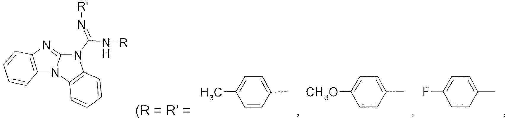


- Kolesnikova, I. V.; Zhurnal Organicheskoi Khimii 25 (1989) 1689-95 describes the synthesis of 5H-benzimidazo[1,2-a]benzimidazole 1,2,3,4,7,8,9,10-octafluoro-5-(2,3,4,5,6-pentafluorophenyl).
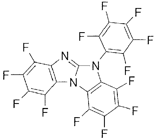
- Achour, Reddouane; Zniber, Rachid, Bulletin des Societes Chimiques Belges 96 (1987) 787-92 describes the synthesis of benzimidazobenzimidazoles
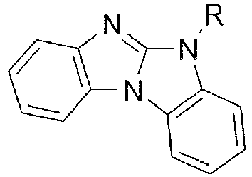
- Hubert, Andre J.; Reimlinger, Hans, Chemische Berichte 103 (1970) 2828-35 describes the synthesis of benzimidazobenzimidazoles


- X. Wang et al. Org. Lett. 2012, 14, 452-455 discloses a highly efficient copper-catalyzed synthesis for compounds of formula
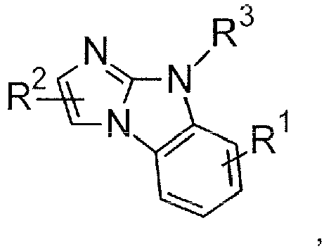
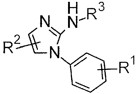
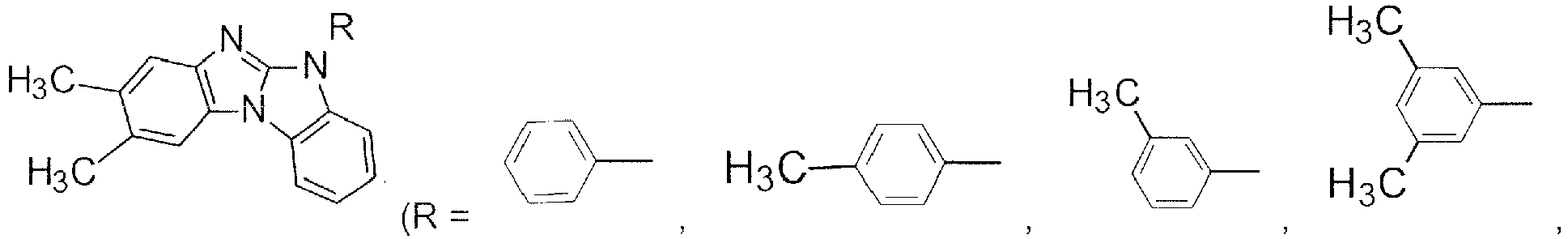

- In Eur. J. Org. Chem. 2014, 5986-5997 a new synthesis of benzimidazolo[1,2-a]benzimidazole is described.
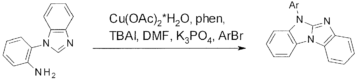
- In RSC Advances 2014, 4, 21904-21908 a new synthesis of benzimidazolo[1,2-a]benzimidazole is described.

-
WO2011/160757 relates to an electronic device comprising an anode, cathode and at least one organic layer which contains a compound of formulae

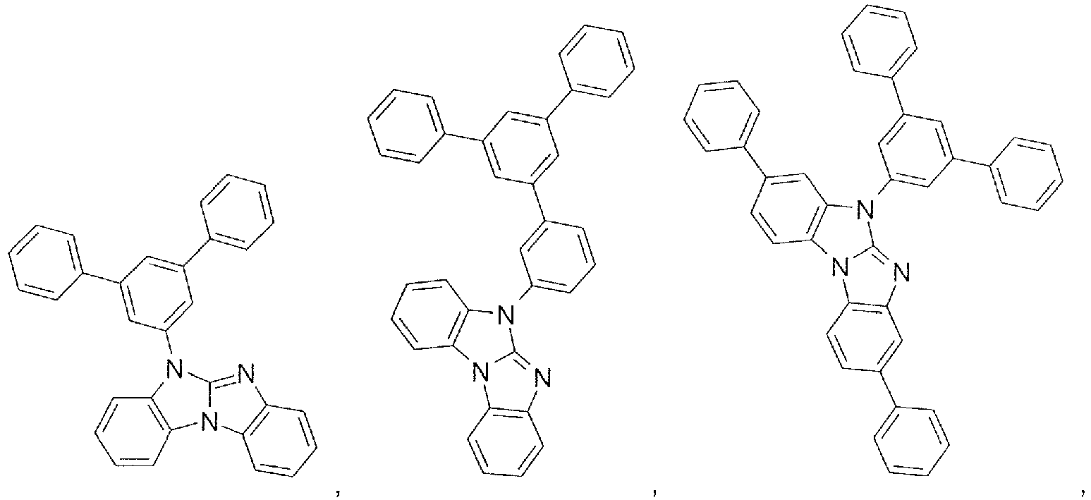
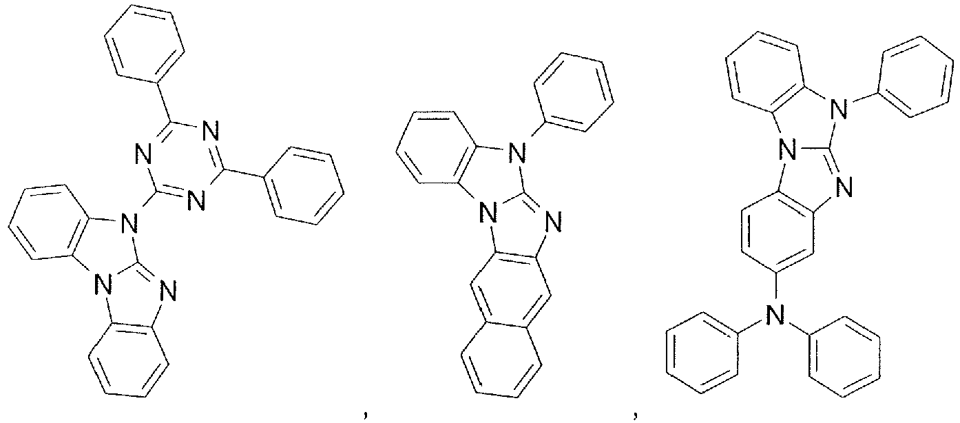
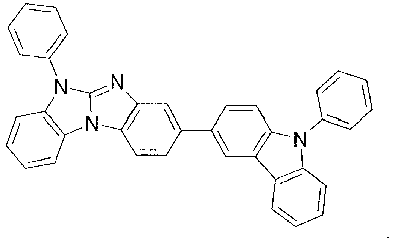
-
WO2012/130709 relates to 4H-Imidazo[1,2-a]imidazoles,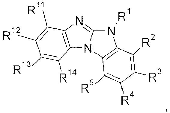
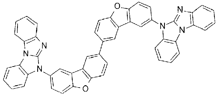
-
WO2013/068376 describes 4H-imidazo[1,2-a]imidazoles of formula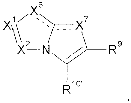


-
WO2014/009317 relates to compounds of formula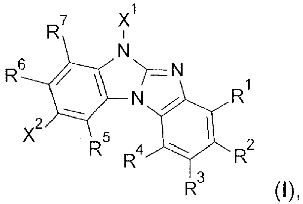

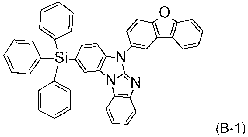
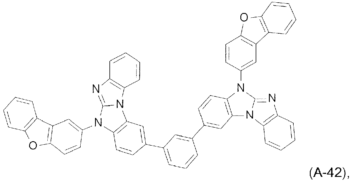
-
WO2014/044722 relates to compounds of formula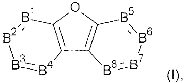
- European patent application no.
13191100.0 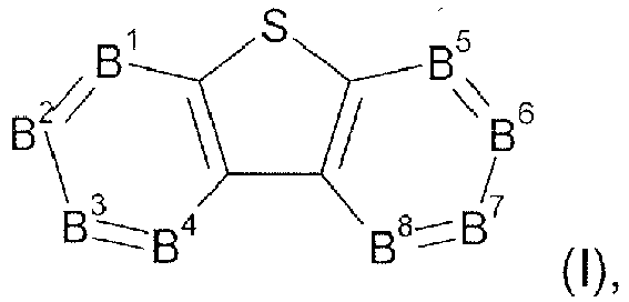
- European patent application no.
14162667.1 

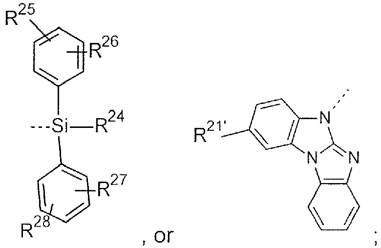
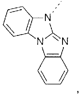
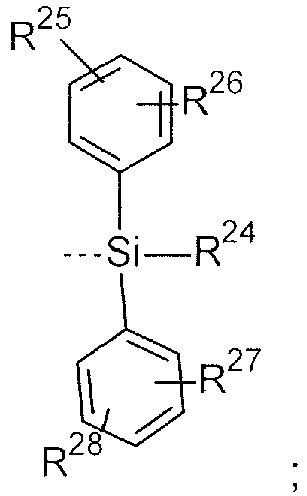
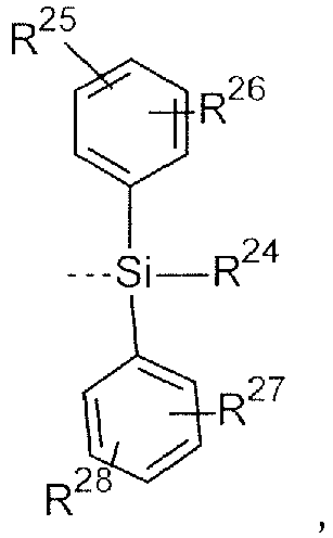
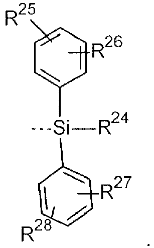
- Benzimidazo[1,2-a]benzimidazo-5-yl and benzimidazo[1,2-a]benzimidazo-2-ylsubstituted benzimidazolo[2,1-b][1,3]benzothiazole derivatives are described in
PCT/EP2014/066174 14183598.3 - European patent application no.
EP14197947.9 
- m is 1, or 2, n is 0, 1, or 2,
- Ar1 and Ar2 are independently of each other a C6-C24aryl group, which can optionally be substituted by G, a C12-C30heteroaryl group, which can optionally be substituted by G,
- A1 is a group of formula
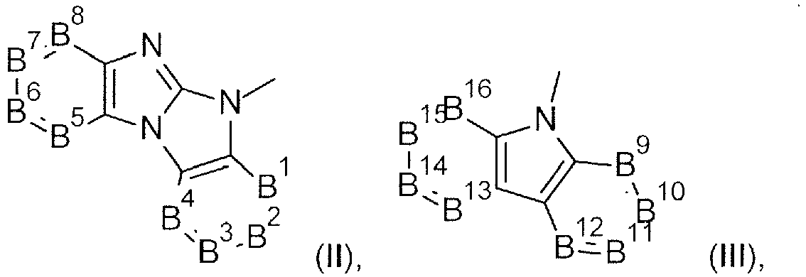
- European patent application no.
EP14193401.8 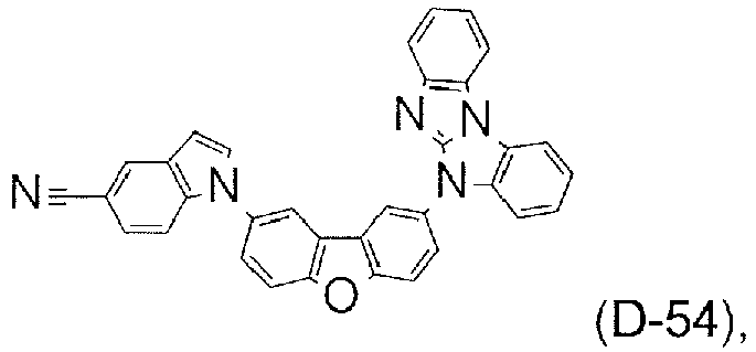
- European patent application no.
EP14197952.6 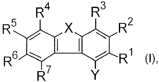
- X is O or S;
- Y is a group of formula -[Ar1]a-[Ar2]b-[Ar3]c-A1;
- A1 is a group of formula

- The following group is described.
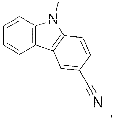
-
WO2013/154064 A1 discloses an organic light emitting element, which has a comopound of the following formula in the light emitting layer:
-
EP 2 039 737 A2 concerns an organic electroluminescence device comprising a compound of formula (I)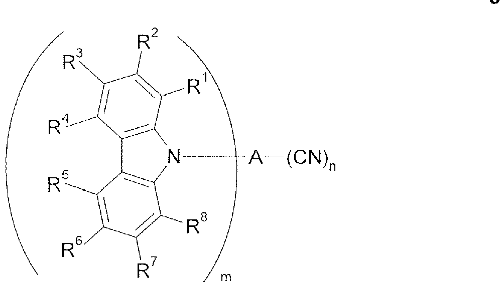
- Neither
WO2013/154064 A1 norEP 2 039 737 A2 disclose compounds comprising benzimidazolo[1,2-a]benzimidazole groups. -
US 2014/0001446 A1 relates to a material for organic EL devices represented by formula (I)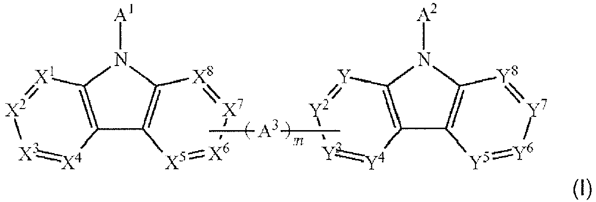
- The material for organic EL devices represented by formula (I) has a central skeleton to which a cyano-substituted aromatic hydrocarbon group or a cyano-substituted heterocyclic group is bonded at a specific position.
- Notwithstanding these developments, there remains a need for organic light emitting devices comprising new materials, especially host (= matrix) materials, charge transport materials and/or charge/exciton blocker materials to provide improved efficiency, stability, manufacturability, driving voltage and/or spectral characteristics of electroluminescent devices. Further, there is a need for materials showing low singlet triplet splitting, which makes them useful as TADF (Thermally Activated Delayed Fluorescence, Adv. Mater. 2014, 26, 7931-7958) emitter or TADF host materials in combination with fluorescent emitters.
- Accordingly, it is an object of the present invention, with respect to the aforementioned prior art, to provide further materials suitable for use in OLEDs and further applications in organic electronics. More particularly, it should be possible to provide charge transport materials, charge/exciton blocker materials and host (= matrix) materials for use in OLEDs. The materials should be suitable especially for OLEDs which comprise at least one emitter, which is preferably a phosphorescence emitter, especially at least one green emitter or at least one blue emitter. It should further be possible to provide materials showing low singlet triplet splitting, which makes them useful as TADF (Thermally Activated Delayed Fluorescence, Adv. Mater. 2014, 26, 7931-7958) emitter or TADF host materials in combination with fluorescent emitters.
- Furthermore, the materials should be suitable for providing OLEDs which ensure good efficiencies, good operative lifetimes and a high stability to thermal stress, and a low use and operating voltage of the OLEDs.
- Said object is solved by compounds of formula (Ib),
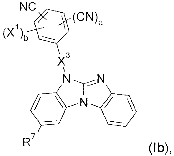
- a is 0 or 1 and b is 0 or 1, whereby the sum of a and b is at least 1;
- X1 is a group of the following formula:


- X3 is a single bond, and
- R7 is H or group of the following formula:
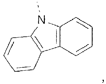
- R70 and R71 are independently of each other a C1-C18alkyl group, a C6-C18aryl group, or a C6-C18aryl group, which is substituted by C1-C18alkyl, and
- R72 is a C1-C18alkyl group, a C6-C18aryl group, or a C6-C18aryl group, which is substituted by C1-C18alkyl.
- The combination of the Benzimidazolo[1,2-a]benzimidazol group having donor action with the nitril group having acceptor action gives rise to materials that are highly suitable in devices that emit green, or blue light. Moreover, the improved ambipolar characteristics give rise to more balanced charge transport in devices resulting in lower voltages and higher external quantum efficiencies (EQE's).
- One key finding of the inventors of the present invention is the relevance of the position of the nitrile group, which is not directly substituted at the benzimidazolo[1,2-a]benzimidazole skeleton, but substituted at the aromatic or heteroaromatic residue X4. Therefore, the compounds of the present invention are characterized by a high acceptor strength, efficient bipolar characteristics and a good suitability as TADF hosts or emitters.
- The compounds of the present invention may be used for electrophotographic photoreceptors, photoelectric converters, organic solar cells (organic photovoltaics), switching elements, such as organic transistors, for example, organic FETs and organic TFTs, organic light emitting field effect transistors (OLEFETs), image sensors, dye lasers and electroluminescent devices, such as, for example, organic light-emitting diodes (OLEDs).
- Accordingly, a further subject of the present invention is directed to an electronic device, comprising a compound according to the present invention. The electronic device is preferably an electroluminescent device, such as an organic light-emitting diode (OLED).
- The compounds of formula Ib can in principal be used in any layer of an EL device, but are preferably used as host, charge transport and/or charge/exciton blocking material. Particularly, the compounds of formula Ib are used as host material for green, especially blue light emitting phosphorescent emitters. Additionally, the compounds of formula Ib are used as TADF emitter or TADF host materials in combination with at least one fluorescent emitter, especially in OLEDs emitting in the blue and green region of the electromagnetic spectrum.
- Hence, a further subject of the present invention is directed to a charge transport layer, comprising a compound of formula Ib according to the present invention.
- A further subject of the present invention is directed to an emitting layer, comprising a compound of formula Ib according to the present invention. In said embodiment a compound of formula Ib is preferably used as host material, more preferably in combination with a phosphorescent emitter.
- A further subject of the present invention is directed to a charge/exciton blocking layer, comprising a compound of formula Ib according to the present invention.
- A further subject of the present invention is directed to an OLED comprising at least one compound of formula Ib as TADF emitter or TADF host material in combination with at least one fluorescent emitter.
- The terms halogen, alkyl, alkoxy, cycloalkyl, aryl, aryloxy, aralkyl, heteroaryl, arylene, heteroarylene generally have the following meaning, if said groups are not further specified in specific embodiments mentioned below:
Halogen is fluorine, chlorine, bromine and iodine. - C1-C25alkyl (C1-C18alkyl) is typically linear or branched, where possible. Examples are methyl, ethyl, n-propyl, isopropyl, n-butyl, sec.-butyl, isobutyl, tert.-butyl, n-pentyl, 2-pentyl, 3-pentyl, 2,2-dimethylpropyl, 1,1,3,3-tetramethylpentyl, n-hexyl, 1-methylhexyl, 1,1,3,3,5,5-hexamethylhexyl, n-heptyl, isoheptyl, 1,1,3,3-tetramethylbutyl, 1-methylheptyl, 3-methylheptyl, n-octyl, 1,1,3,3-tetramethylbutyl and 2-ethylhexyl, n-nonyl, decyl, undecyl, dodecyl, tridecyl, tetradecyl, pentadecyl, hexadecyl, heptadecyl, or octadecyl. C1-C8alkyl is typically methyl, ethyl, n-propyl, isopropyl, n-butyl, sec.-butyl, isobutyl, tert.-butyl, n-pentyl, 2-pentyl, 3-pentyl, 2,2-dimethyl-propyl, n-hexyl, n-heptyl, n-octyl, 1,1,3,3-tetramethylbutyl and 2-ethylhexyl. C1-C4alkyl is typically methyl, ethyl, n-propyl, isopropyl, n-butyl, sec.-butyl, isobutyl, tert.-butyl.
- C1-C25alkoxy groups (C1-C18alkoxy groups) are straight-chain or branched alkoxy groups, e.g. methoxy, ethoxy, n-propoxy, isopropoxy, n-butoxy, sec-butoxy, tert-butoxy, amyloxy, isoamyloxy or tert-amyloxy, heptyloxy, octyloxy, isooctyloxy, nonyloxy, decyloxy, undecyloxy, dodecyloxy, tetradecyloxy, pentadecyloxy, hexadecyloxy, heptadecyloxy and octadecyloxy. Examples of C1-C8alkoxy are methoxy, ethoxy, n-propoxy, isopropoxy, n-butoxy, sec.-butoxy, isobutoxy, tert.-butoxy, n-pentyloxy, 2-pentyloxy, 3-pentyloxy, 2,2-dimethylpropoxy, n-hexyloxy, n-heptyloxy, n-octyloxy, 1,1,3,3-tetramethylbutoxy and 2-ethylhexyloxy, preferably C1-C4alkoxy such as typically methoxy, ethoxy, n-propoxy, isopropoxy, n-butoxy, sec.-butoxy, isobutoxy, tert.-butoxy.
- The term "cycloalkyl group" is typically C5-C12cycloalkyl, such as cyclopentyl, cyclohexyl, cycloheptyl, cyclooctyl, cyclononyl, cyclodecyl, cycloundecyl, cyclododecyl, preferably cyclopentyl, cyclohexyl, cycloheptyl, or cyclooctyl, which may be unsubstituted or substituted.
- C6-C24aryl (preferably C6-C18aryl), which optionally can be substituted, is typically phenyl, 4-methylphenyl, 4-methoxyphenyl, naphthyl, especially 1-naphthyl, or 2-naphthyl, biphenylyl, ter-phenylyl, pyrenyl, 2- or 9-fluorenyl, phenanthryl, or anthryl, which may be unsubstituted or substituted. Phenyl, 1-naphthyl and 2-naphthyl are examples of a C6-C10aryl group.
- C6-C24aryloxy, which optionally can be substituted, is typically C6-C10aryloxy, which optionally can be substituted by one, or more C1-C8alkyl and/or C1-C8alkoxy groups, such as, for example, phenoxy, 1-naphthoxy, or 2-naphthoxy.
- C7-C25aralkyl is typically benzyl, 2-benzyl-2-propyl, β-phenyl-ethyl, α,α-dimethylbenzyl, ω-phenyl-butyl, ω,ω-dimethyl-ω-phenyl-butyl, ω-phenyl-dodecyl, ω-phenyl-octadecyl, ω-phenyl-eicosyl or ω-phenyl-docosyl, preferably C7-C18aralkyl such as benzyl, 2-benzyl-2-propyl, β-phenyl-ethyl, α,α-dimethylbenzyl, ω-phenyl-butyl, ω,ω-dimethyl-ω-phenyl-butyl, ω-phenyl-dodecyl or ω-phenyl-octadecyl, and particularly preferred C7-C12aralkyl such as benzyl, 2-benzyl-2-propyl, β-phenyl-ethyl, α,α-dimethylbenzyl, ω-phenyl-butyl, or ω,ω-dimethyl-ω-phenyl-butyl, in which both the aliphatic hydrocarbon group and aromatic hydrocarbon group may be unsubstituted or substituted. Preferred examples are benzyl, 2-phenylethyl, 3-phenylpropyl, naphthylethyl, naphthylmethyl, and cumyl.
- C2-C30heteroaryl (preferably C2-C13 heteroarylaryl) represents a ring with five to seven ring atoms or a condensed ring system, wherein nitrogen, oxygen or sulfur are the possible hetero atoms, and is typically a heterocyclic group with five to 30 atoms having at least six conjugated π-electrons such as thienyl, benzothiophenyl, dibenzothiophenyl, thianthrenyl, furyl, furfuryl, 2H-pyranyl, benzofuranyl, isobenzofuranyl, dibenzofuranyl, phenoxythienyl, pyrrolyl, imidazolyl, pyrazolyl, pyridyl, bipyridyl, triazinyl, pyrimidinyl, pyrazinyl, pyridazinyl, indolizinyl, isoindolyl, indolyl, indazolyl, purinyl, quinolizinyl, chinolyl, isochinolyl, phthalazinyl, naphthyridinyl, chinoxalinyl, chinazolinyl, cinnolinyl, pteridinyl, carbazolyl, carbolinyl, benzotriazolyl, benzoxazolyl, phenanthridinyl, acridinyl, pyrimidinyl, phenanthrolinyl, phenazinyl, isothiazolyl, phenothiazinyl, isoxazolyl, furazanyl, 4-imidazo[1,2-a]benzimidazoyl, 5-benzimidazo[1,2-a]benzimidazoyl, benzimidazolo[2,1-b][1,3]benzothiazolyl, carbazolyl, or phenoxazinyl, which can be unsubstituted or substituted. Benzimidazo[1,2-a]benzimidazo-5-yl, benzimidazo[1,2-a]benzimidazo-2-yl, carbazolyl and dibenzofuranyl are examples of a C2-C14heteroaryl group.
- A C2-C13heteroaryl group is for example, benzimidazo[1,2-a]benzimidazo-5-yl

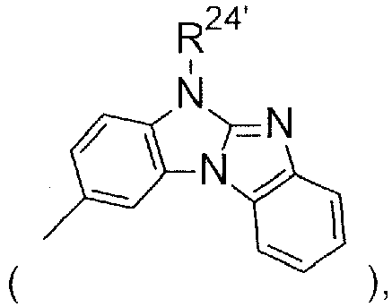
- C2-C30heteroaryl (preferably C2-C13 heteroarylaryl) means that the heteroaryl residue comprises at least 2 carbon atoms and at most 30 carbon atoms in the base skeleton (without substituents). The further atoms in the heteroaryl base skeleton are heteroatoms (N, O and/or S).
- R24 is in each case independently C1-C18alkyl, such as methyl, ethyl, n-propyl, iso-propyl, n-butyl, isobutyl, sec-butyl, hexyl, octyl, or 2-ethyl-hexyl, or C6-C14aryl, such as phenyl, tolyl, naphthyl, phenanthronyl, triphenylenyl, fluoranthenyl or biphenylyl.
- C6-C24arylene groups, which optionally can be substituted by G, are typically phenylene, 4-methylphenylene, 4-methoxyphenylene, naphthylene, especially 1-naphthylene, or 2-naphthylene, biphenylylene, terphenylylene, pyrenylene, 2- or 9-fluorenylene, phenanthrylene, or anthrylene, which may be unsubstituted or substituted. Preferred C6-C24arylen groups are 1,3-phenylene, 3,3'-biphenylylene, 3,3'-m-terphenylene, 2- or 9-fluorenylene, phenanthrylene, which may be unsubstituted or substituted.
- C2-C30heteroarylene groups, which optionally can be substituted by G, represent a ring with five to seven ring atoms or a condensed ring system, wherein nitrogen, oxygen or sulfur are the possible hetero atoms, and is typically a heterocyclic group with five to 30 atoms having at least six conjugated -electrons such as thienylene, benzothiophenylene, dibenzothiophenylene, thianthrenylene, furylene, furfurylene, 2H-pyranylene, benzofuranylene, isobenzofuranylene, dibenzofuranylene, phenoxythienylene, pyrrolylene, imidazolylene, pyrazolylene, pyridylene, bipyridylene, triazinylene, pyrimidinylene, pyrazinylene, pyridazinylene, indolizinylene, isoindolylene, indolylene, indazolylene, purinylene, quinolizinylene, chinolylene, isochinolylene, phthalazinylene, naphthyridinylene, chinoxalinylene, chinazolinylene, cinnolinylene, pteridinylene, carbolinylene, benzotriazolylene, benzoxazolylene, phenanthridinylene, acridinylene, pyrimidinylene, phenanthrolinylene, phenazinylene, isothiazolylene, phenothiazinylene, isoxazolylene, furazanylene, carbazolylene, benzimidazo[1,2-a]benzimidazo-2,5-ylene, or phenoxazinylene, which can be unsubstituted or substituted. Preferred C2-C30heteroarylen groups are pyridylene, triazinylene, pyrimidinylene, carbazolylene, dibenzofuranylene and benzimidazo[1,2-a]benzimidazo-2,5-ylene

- Possible preferred substituents of the above-mentioned groups are C1-C8alkyl, a hydroxyl group, a mercapto group, C1-C8alkoxy, C1-C8alkylthio, halogen, halo-C1-C8alkyl, or a cyano group.
- The C6-C24aryl (C6-C18aryl) and C2-C30heteroaryl groups are preferably substituted by one, or more C1-C8alkyl groups.
- If a substituent occurs more than one time in a group, it can be different in each occurrence.
- Halo-C1-C8alkyl is an alkyl group where at least one of the hydrogen atoms is replaced by a halogen atom. Examples are -CF3, -CF2CF3, -CF2CF2CF3, -CF(CF3)2, -(CF2)3CF3, and -C(CF3)3.
- The wording "substituted by G" means that one, or more, especially one to three substituents G might be present.
- G is preferably -OR69, -SR69, -NR65R66; a C1-C18alkyl group, a C6-C14aryl group, a C6-C14aryl group, which is substituted by F, or C1-C18alkyl; a C2-C13heteroaryl group, or a C2-C13heteroaryl group, which is substituted by F, or C1-C18alkyl; wherein R65, R66 and R69 are independently of each other C1-C18alkyl, such as methyl, ethyl, n-propyl, iso-propyl, n-butyl, isobutyl, sec-butyl, hexyl, octyl, or 2-ethyl-hexyl, or C6-C14aryl, such as phenyl, tolyl, naphthyl, or biphenylyl.
- In the compounds of the invention,
a is 0 or 1, b is 0 or 1,
and the sum of a + b is at least1. - In one preferred embodiment, especially in the case that the compounds of formula Ib are used TADF emitters or TADF host materials in combination with fluorescent emitters, a is preferably 0.
- X3 is a single bond.
- R7 is H or a group of the following formula:

- R70 and R71 are independently of each other a C1-C18alkyl group, a C6-C18aryl group, or a C6-C18aryl group, which is substituted by C1-C18alkyl, and
R72 is a C1-C18alkyl group, a C6-C18aryl group, or a C6-C18aryl group, which is substituted by C1-C18alkyl; preferably, R70, R71 and R72 are phenyl. - Specific examples of the compounds represented by the formula (Ib) are given below. The compounds represented by the formula (Ib) are not limited to the following specific examples.
- Suitable compounds of the invention are:
-
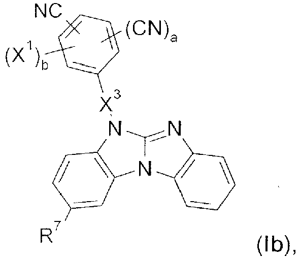
-
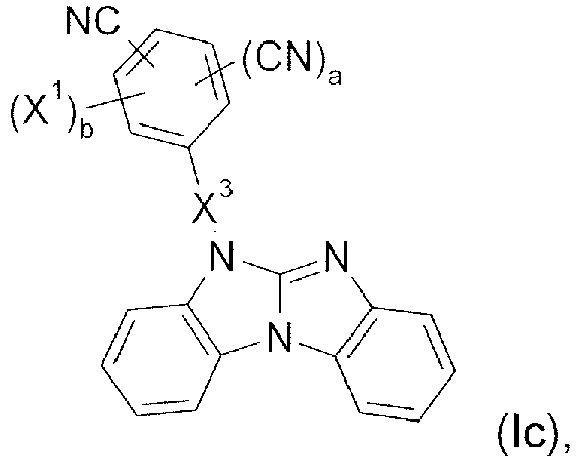
- In the compounds of formula (Ib), the residues and indices have the following meaning:
- a is 0 or 1 and b is 0 or 1, whereby the sum of a and b is at least 1;
- X1 is a group of the following formula:
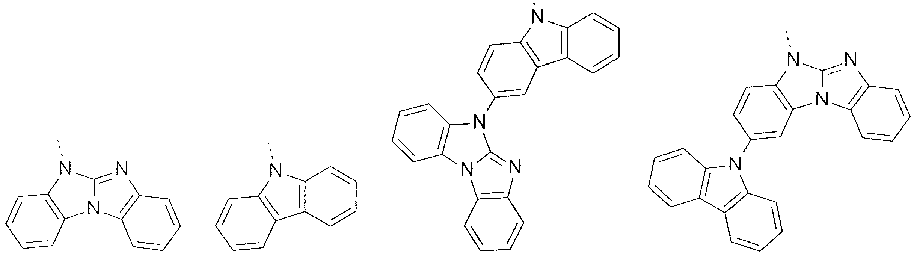
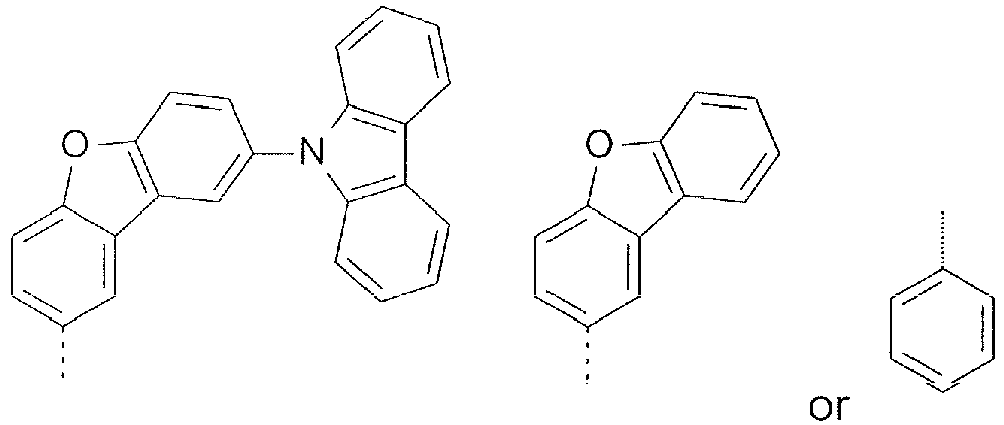
- X3 is a single bond, and
- R7 is H or group of the following formula:
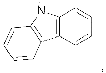
- R70 and R71 are independently of each other a C1-C18alkyl group, a C6-C18aryl group, or a C6-C18aryl group, which is substituted by C1-C18alkyl, and
- R72 is a C1-C18alkyl group, a C6-C18aryl group, or a C6-C18aryl group, which is substituted by C1-C18alkyl; preferably, R70, R71 and R72 are phenyl.
- The compounds of formula (Ib) are preferably compounds of formula (Ib')
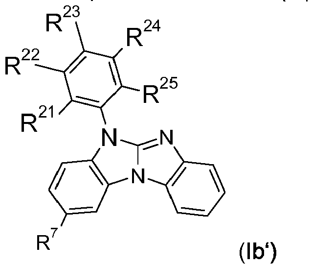
- wherein R7 is defined above and below; and
- R21, R22, R23, R24 and R25
are CN,
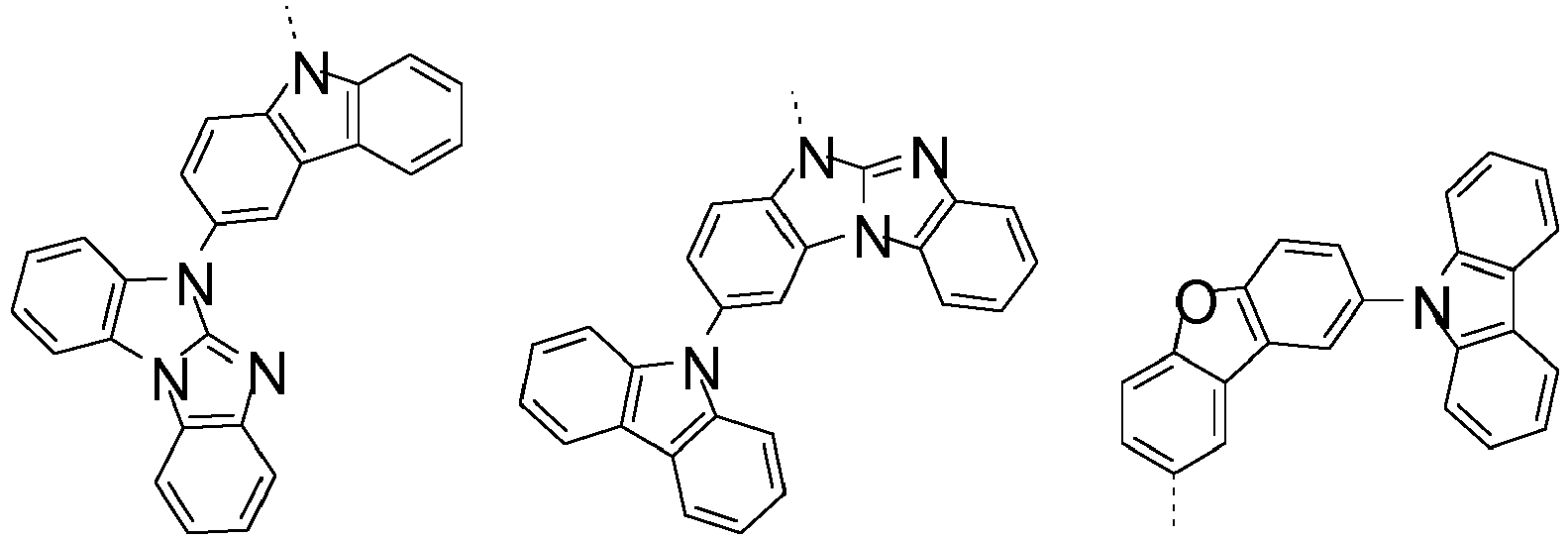
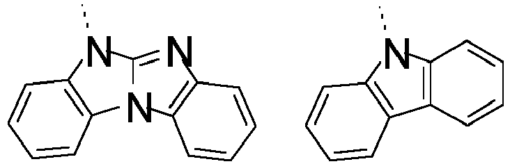
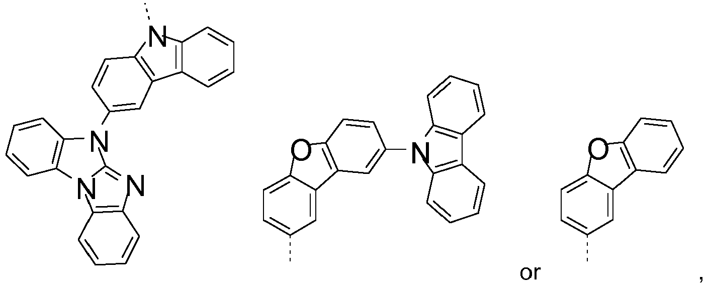
- wherein 1 or 2 of the residues R21, R22, R23, R24 and R25 are CN.
- In the compounds of formula (Ic), the residues and indices have the following meaning: a is 0 or 1 and b is 0 or 1, whereby the sum of a and b is at least 1;
X1 is a group of the following formula: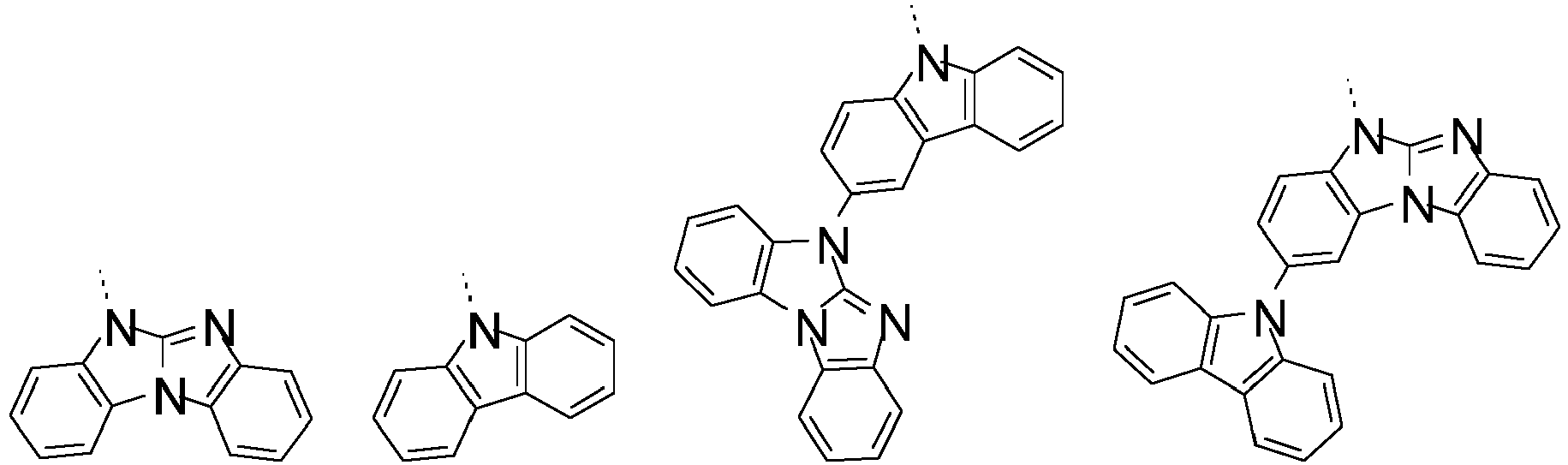
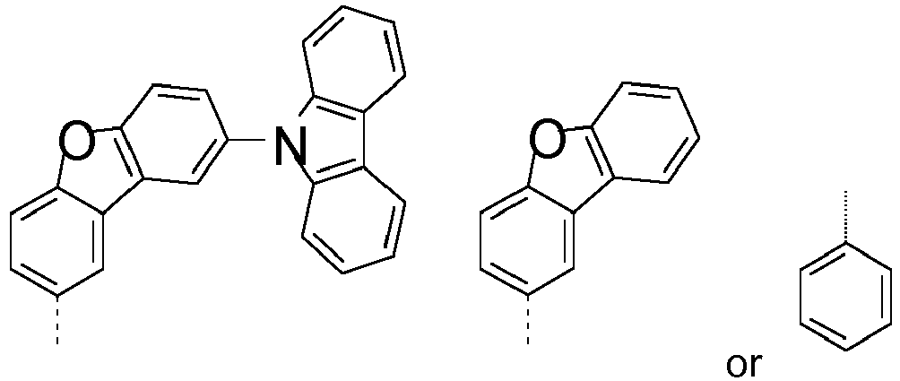
- The compounds of formula (Ic) are preferably compounds of formula (Ic')
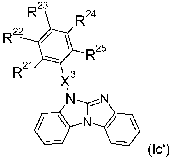
- wherein X3 is a single bond; and
- R21, R22, R23, R24 and R25 are CN,
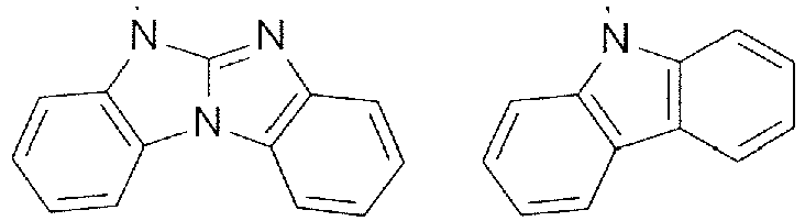


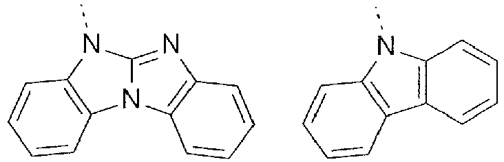

- Preferred compounds of formulae (Ib') and (Ic') are mentioned in the following tables, whereby the 5th and the 25th compound of the first table do not fall within the scope of formula (Ic') and the 5th compound of the second table does not fall within the scope of formula (Ib'). These compounds are for reference only:
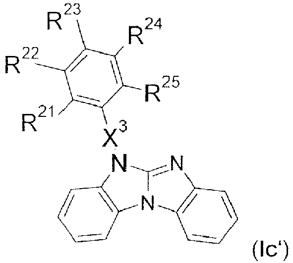
Nr. R21 R22 R23 R24 R25 X3 CN CN H H H - CN H CN H H - CN H H CN H - CN H H H CN - CN H H H H - H CN CN H H - H CN H CN H - H CN H H CN - CN Ar1 H H H - CN H Ar1 H H - CN H H Ar1 H - CN H H H Ar1 - CN Ar2 H H H - CN H Ar2 H H - CN H H Ar2 H - CN H H H Ar2 - CN Ar3 H H H - CN H Ar3 H H - CN H H Ar3 H - CN H H H Ar3 - CN Ar4 H H H - CN H Ar4 H H - CN H H Ar4 H - CN H H H Ar4 - CN H H H H - H CN CN H Ar1 - Ar1 CN CN H H - CN Ar5 H H H - CN H Ar5 H H - CN H H Ar5 H - CN H H H Ar5 - Ar1 : 

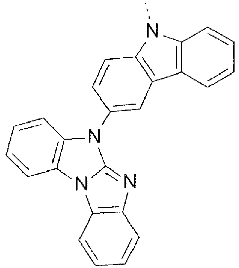

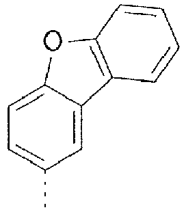

Nr. R21 R22 R23 R24 R25 R7 CN CN H H H Ar2 CN H CN H H Ar2 CN H H CN H Ar2 CN H H H CN Ar2 CN H H H H Ar2 H CN CN H H Ar2 H CN H CN H Ar2 H CN H H CN Ar2 CN CN H H H Ar2 CN H CN H H Ar2 CN H H CN H Ar2 CN H H H CN Ar2 H CN CN H H Ar2 H CN H CN H Ar2 H CN H H CN Ar2 CN Ar2 H H H Ar2 CN H Ar2 H H Ar2 CN H H Ar2 H Ar2 CN H H H Ar2 Ar2 CN Ar5 H H H Ar2 CN H Ar5 H H Ar2 CN H H Ar5 H Ar2 CN H H H Ar5 Ar2 Ar2: 
- Further specific examples of formula (Ib) are the following compounds, whereby the 2nd and 3rd compound in the 2nd line on page 23 are for reference only:
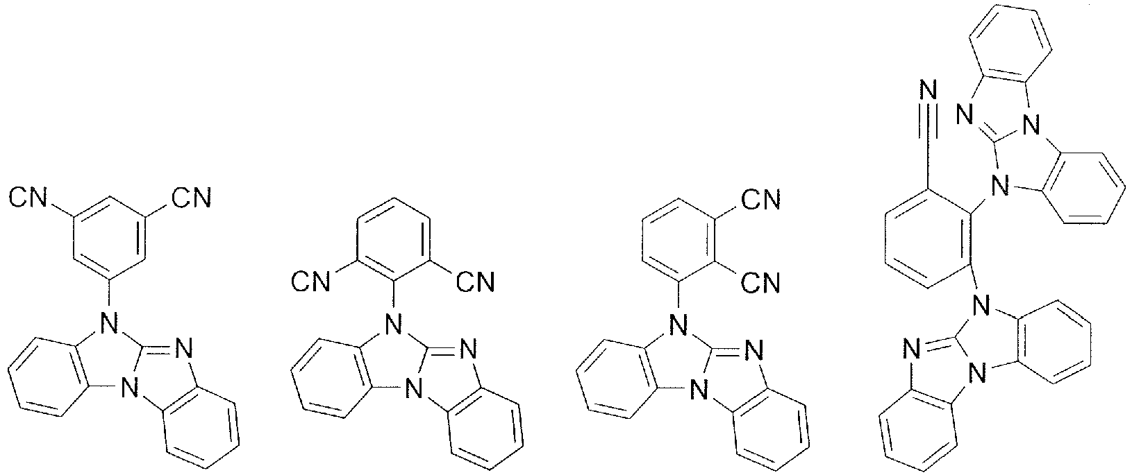
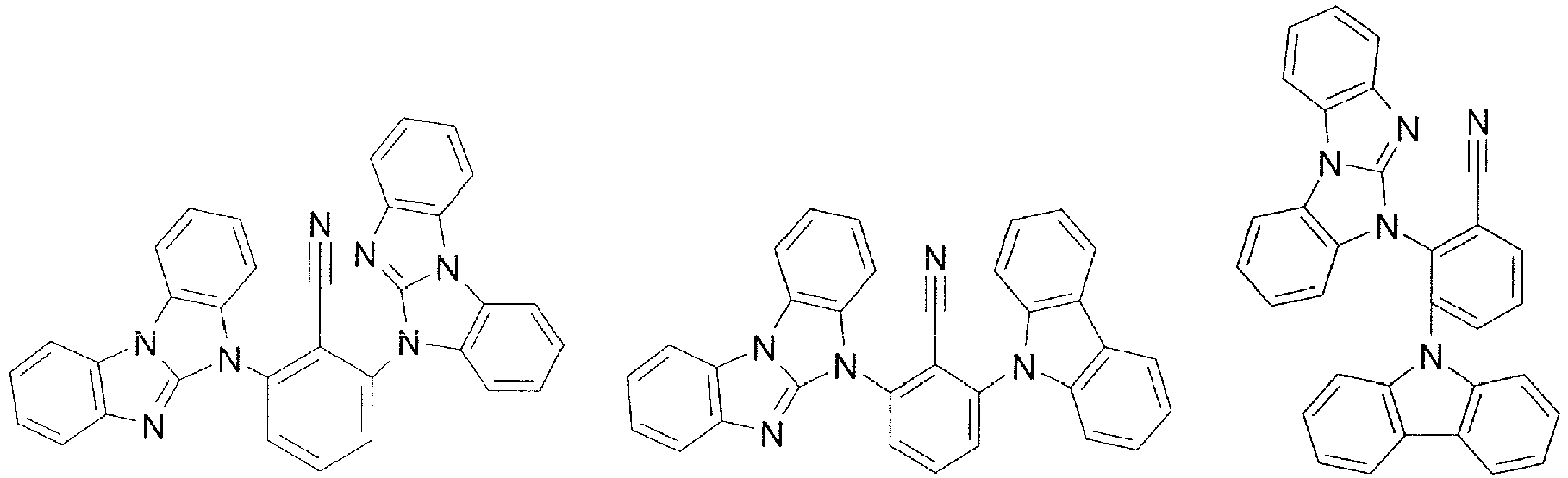
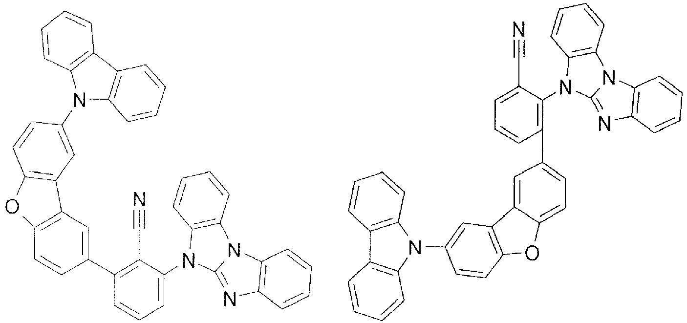
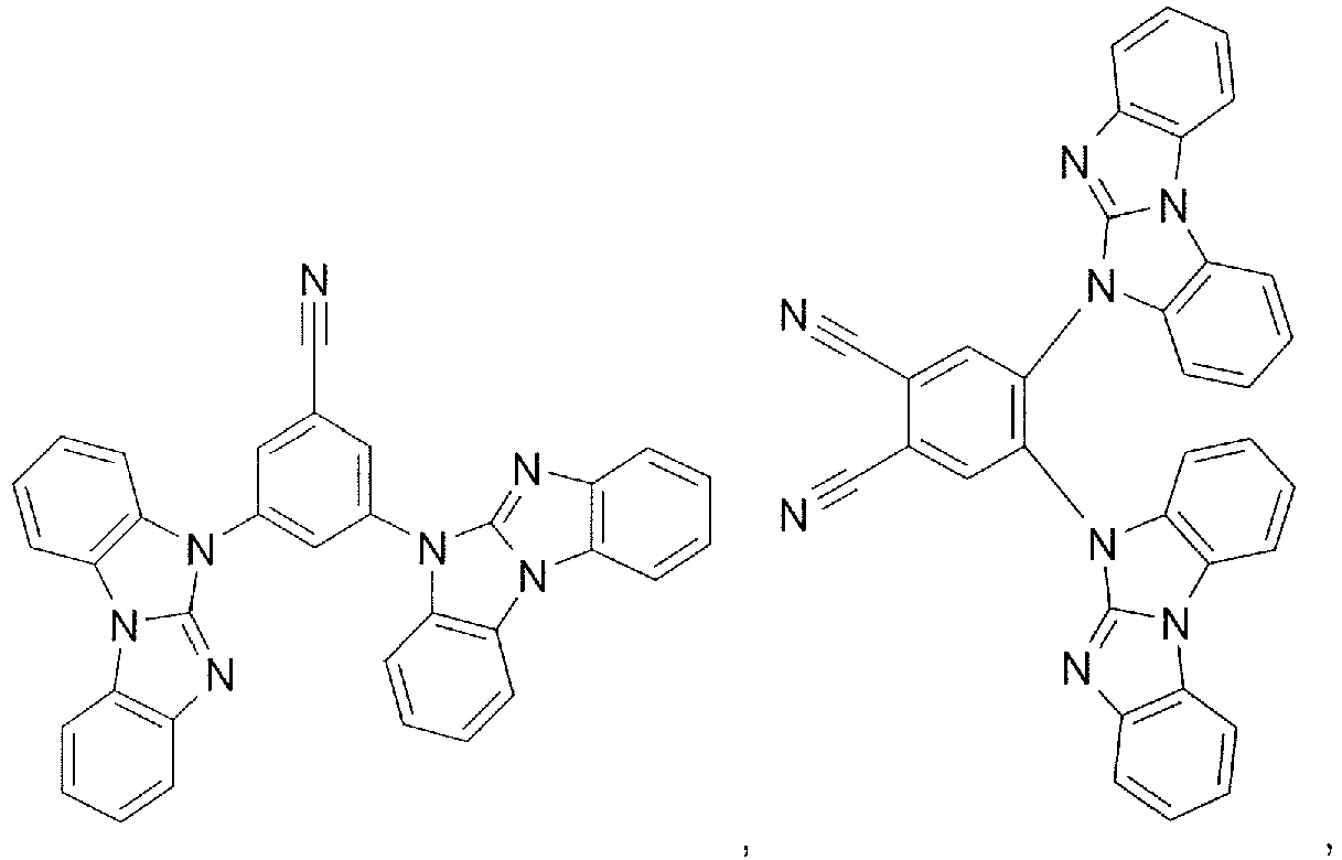
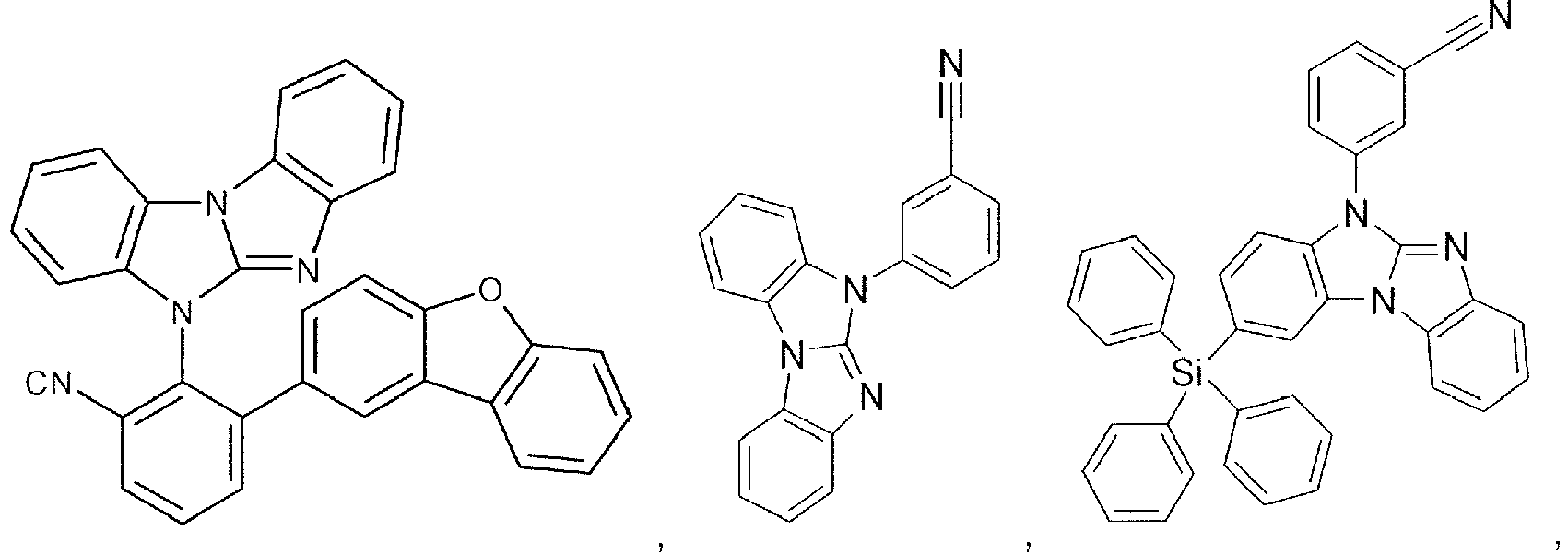
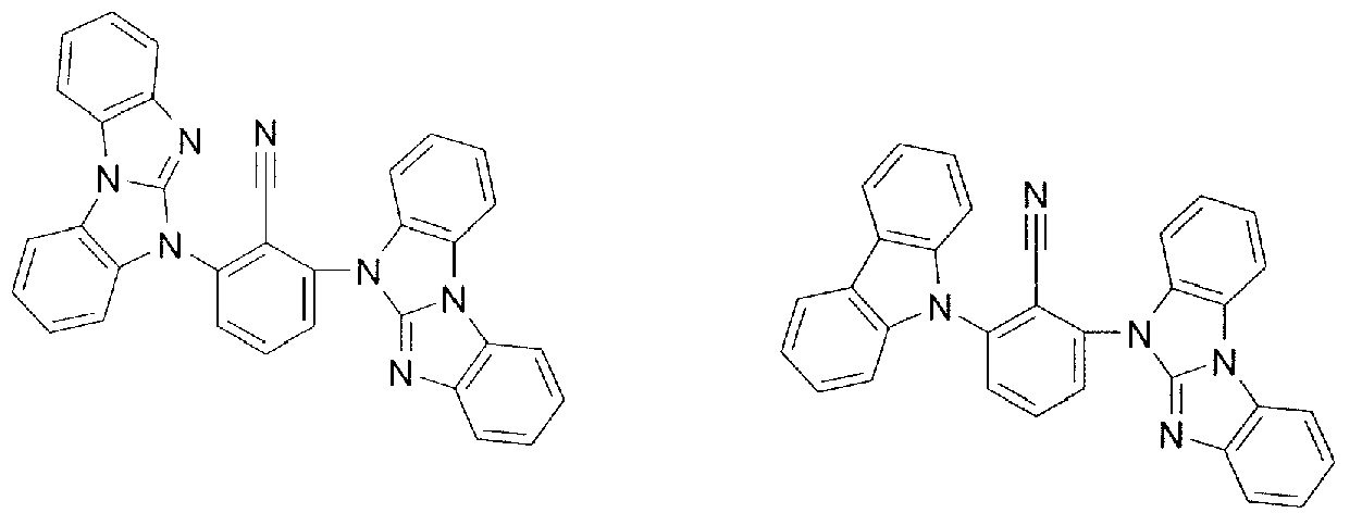
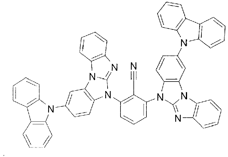
- The specific aryl-nitrile or heteroaryl- nitrile benzimidazolo[1,2-a]benzimidazoles derivatives of the present invention are found to be suitable for use in organo-electroluminescent devices. In particular, certain aryl-nitrile or heteroaryl- nitrile benzimidazolo[1,2-a]benzimidazoles derivatives are suitable host materials, especially host materials for phosphorescent emitters, charge transport materials and/or charge/exciton blocker materials with good efficiency and durability.
- Also, said aryl-nitrile or heteroaryl- nitrile benzimidazolo[1,2-a]benzimidazoles show low singlet triplet splitting, which makes them useful as TADF (Thermally Activated Delayed Fluorescence, Adv. Mater. 2014, 26, 7931-7958) emitter or TADF host materials in combination with fluorescent emitters. The TADF emitter or TADF host materials can be used together with one or more additional host materials.
- The combination of the benzimidazolo[1,2-a]benzimidazole groups with the cyano group in the specific position of the benzimidazolo[1,2-a]benzimidazole gives rise to materials that are highly suitable in devices that emit green, or blue light. Moreover, the improved ambipolar characteristics give rise to more balanced charge transport in devices resulting in lower voltages and higher external quantum efficiencies (EQE's).
- One key finding of the inventors of the present invention is the relevance of the position of the nitrile group, which is not directly substituted at the benzimidazolo[1,2-a]benzimidazole skeleton. Therefore, the compounds of the present invention are characterized by a high acceptor strength, efficient bipolar characteristics and a good suitability as TADF hosts or emitters.
- The compounds of the present invention may be used for electrophotographic photoreceptors, photoelectric converters, organic solar cells (organic photovoltaics), switching elements, such as organic transistors, for example, organic FETs and organic TFTs, organic light emitting field effect transistors (OLEFETs), image sensors, dye lasers and electroluminescent devices (EL devices), such as, for example, organic light-emitting diodes (OLEDs). Preferably, the compounds of the present invention are used in electroluminescent devices, especially in OLEDs.
- Accordingly, a further subject of the present invention is directed to an electronic device, comprising a compound according to the present invention. The electronic device is preferably an electroluminescent device (EL-device), especially an OLED.
- The compounds of formula Ib can in principal be used in any layer of an EL device, but are preferably used as host, charge transport and/or charge/exciton blocking material. Particularly, the compounds of formula Ib are used as host material for green, especially blue light emitting emitters, which are preferably phosphorescent emitters.
- Hence, a further subject of the present invention is directed to a charge transport layer comprising a compound of formula Ib according to the present invention.
- A further subject of the present invention is directed to an emitting layer, comprising a compound of formula Ib according to the present invention. In said embodiment a compound of formula Ib is preferably used as host material in combination with an emitter, which is preferably a phosphorescent emitter.
- A further subject of the present invention is directed to a charge/exciton blocking layer, comprising a compound of formula Ib according to the present invention.
- Formula (I) i.a. encompasses the compounds of the invention, namely the compounds of formula (Ib).
- The synthesis of the compounds of formula (I) can be carried out in analogy to the synthesis of benzimidazolo[1,2-a]benzimidazoles mentioned in the prior art.
- The synthesis of
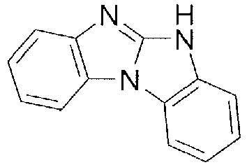
- The introduction of the group -X3-X4-CN (N-arylation) is generally carried out by reacting the base skeleton
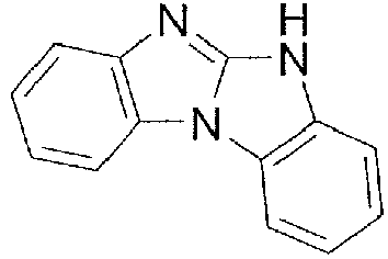
- The nucleophilic aromatic substitution (N-arylation) of
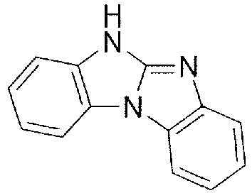
- The nucleophilic aromatic substitution (N-arylation) can be performed in solvent or in a melt. Preferably, the reaction is carried out in a solvent. Suitable solvents are, for example, (polar) aprotic solvents such as dimethyl sulfoxide (DMSO), dimethylformamide (DMF), N-methyl-2-pyrrolidone (NMP) or dimethylacetamide (DMA).
- The reaction temperature is strongly dependent on the reactivity of the aryl fluoride. The reaction (N-arylation) is preferably carried out at a temperature of -10 to 220 °C, more preferably 60 to 150 °C.
- Ullmann reaction (N-arylation) of

- Reaction conditions for Ullmann reactions are, for example, described in Angew Chem Int Ed Engl., 48 (2009) 6954-71
WO14009317 WO12130709 - Typically the Ullmann coupling of the compound of formula
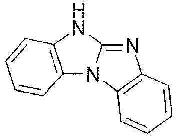
- The N-arylation is, for example, disclosed in H. Gilman and D. A. Shirley, J. Am. Chem. Soc. 66 (1944) 888; D. Li et al., Dyes and Pigments 49 (2001) 181 - 186 and Eur. J. Org. Chem. (2007) 2147-2151.
- An example for an N-arylation of the
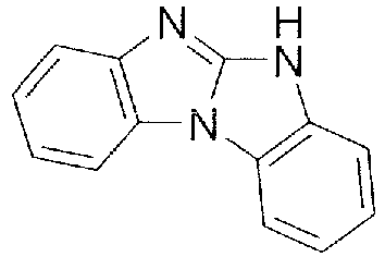
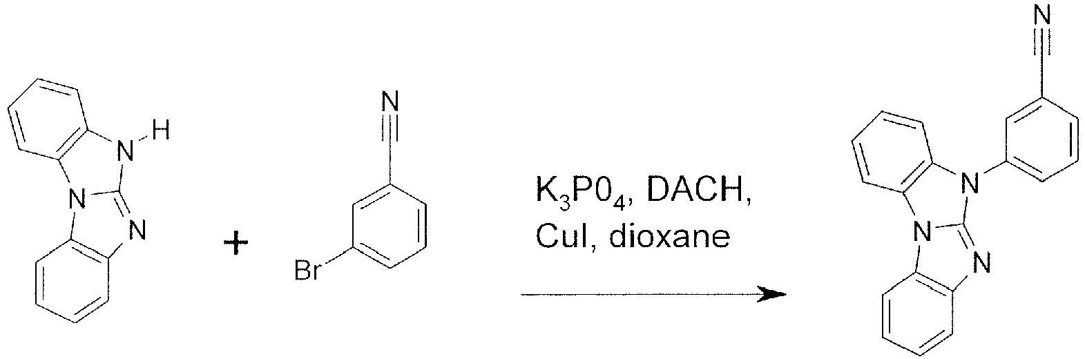
- DACH is (±)-trans-1,2-diaminocyclohexane
- The synthesis of

WO12130709 - The groups Hal-X3-X4-CN are commercially available or prepared by processes known in the art. Suitable preparation processes fore some groups Hal-X3-X4-CN are mentioned in the following.
- Suitable base skeletons of the formula
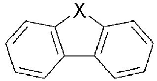
WO2010079051 andEP1885818 . - The halogenation of said base skeletons

- Optionally substituted dibenzofurans, dibenzothiophenes and carbazoles can be dibrominated in the 2,8 positions (dibenzofuran and dibenzothiophene) or 3,6 positions (carbazole) with bromine or NBS in glacial acetic acid or in chloroform. For example, the bromination with Br2 can be effected in glacial acetic acid or chloroform at low temperatures, e.g. 0°C. Suitable processes are described, for example, in M. Park, J.R. Buck, C.J. Rizzo, Tetrahedron, 54 (1998) 12707-12714 for X= NPh, and in W. Yang et al., J. Mater. Chem. 13 (2003) 1351 for X= S. In addition, 3,6-dibromocarbazole, 3,6-dibromo-9-phenylcarbazole, 2,8-dibromodibenzothiophene, 2,8-dibromodibenzofuran, 2-bromocarbazole, 3-bromodibenzothiophene, 3-bromodibenzofuran, 3-bromocarbazole, 2-bromodibenzothiophene and 2-bromodibenzofuran are commercially available.
- Monobromination in the 4 position of dibenzofuran (and analogously for dibenzothiophene) is described, for example, in J. Am. Chem. Soc. 1984, 106, 7150. Dibenzofuran (dibenzothiophene) can be monobrominated in the 3 position by a sequence known to those skilled in the art, comprising a nitration, reduction and subsequent Sandmeyer reaction.
- Monobromination in the 2 position of dibenzofuran or dibenzothiophene and monobromination in the 3 position of carbazole are effected analogously to the dibromination, with the exception that only one equivalent of bromine or NBS is added.
- For the nucleophilic substitution, Cl- or F-substituted dibenzofurans, dibenzothiophenes and carbazoles are preferred. The chlorination is described, inter alia, in J. Heterocyclic Chemistry, 34 (1997) 891-900, Org. Lett., 6 (2004) 3501-3504; J. Chem. Soc. [Section] C: Organic, 16 (1971) 2775-7, Tetrahedron Lett. 25 (1984) 5363-6, J. Org. Chem. 69 (2004) 8177-8182. The fluorination is described in J. Org. Chem. 63 (1998) 878-880 and J. Chem. Soc., Perkin Trans. 2, 5 (2002) 953-957.
- Introduction of the

- The introduction of the
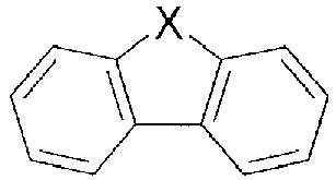
- Examples for a copper catalyzed coupling are (see also Example 7B and 8A in the Example part):
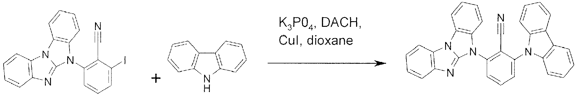
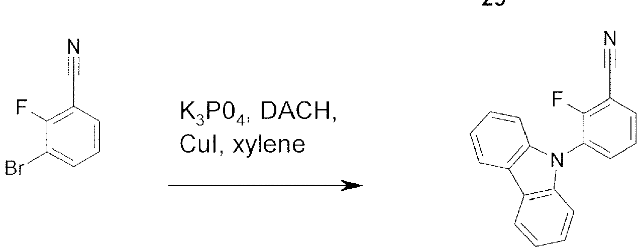
- DACH is (±)-trans-1,2-diaminocyclohexane
- Alternatively, the introduction of the
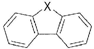
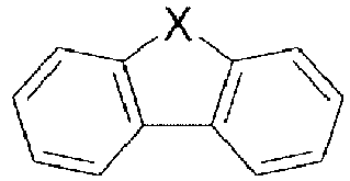
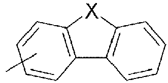

- Examples for a Pd catalyzed coupling are (see also Examples 9B and 10B in the Example part):
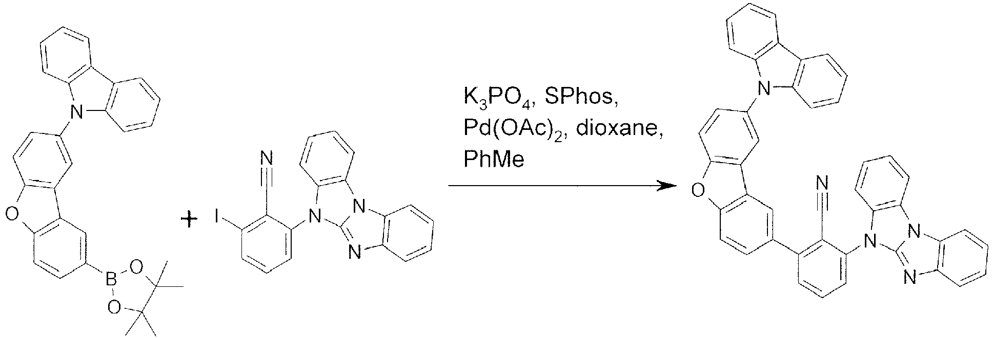
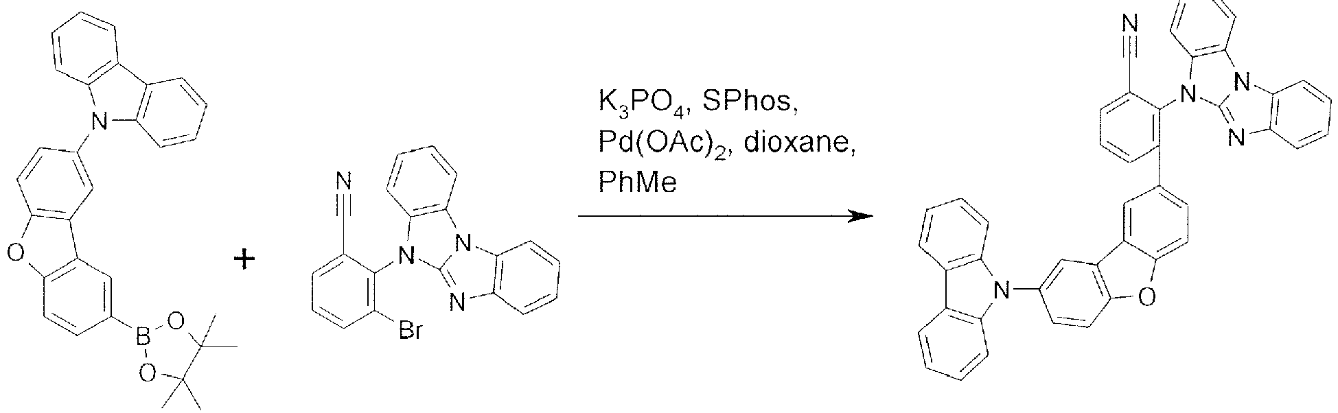
- Diboronic acid or diboronate group containing dibenzofurans, dibenzothiophenes and carbazoles can be readily prepared by an increasing number of routes. An overview of the synthetic routes is, for example, given in Angew. Chem. Int. Ed. 48 (2009) 9240 - 9261.
- By one common route diboronic acid or diboronate group containing dibenzofurans, dibenzothiophenes, and carbazoles can be obtained by reacting halogenated dibenzofurans, dibenzothiophenes and carbazoles with (Y1O)2B-B(OY1)2,
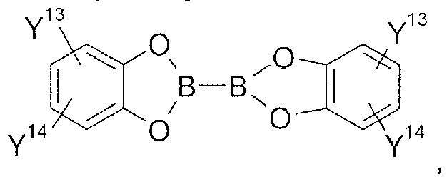

- Diboronic acid or diboronate group containing dibenzofurans, dibenzothiophenes and carbazoles can also be prepared by reacting halogenated dibenzofurans, dibenzothiophenes and carbazoles with alkyl lithium reagents, such as, for example, n-butyl lithium, or t-buthyl lithium, followed by reaction with boronic esters, such as, for example, B(isopropoxy)3, B(methoxy)3, or
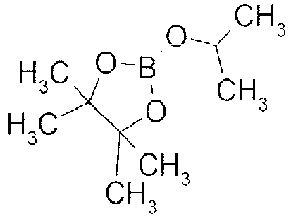
- Diboronic acid or diboronate group containing dibenzofurans, dibenzothiophenes and carbazoles can also be prepared by reacting dibenzofurans, dibenzothiophenes and carbazoles with lithium amides, such as, for example, lithium diisopropylamide (LDA) followed by reaction with boronic esters such as, for example, B(isopropoxy)3, B(methoxy)3, or
- It has been found that the compounds of the formula Ib are particularly suitable for use in applications in which charge carrier conductivity is required, especially for use in organic electronics applications, for example selected from switching elements such as organic transistors, e.g. organic FETs and organic TFTs, organic solar cells and organic light-emitting diodes (OLEDs).
- The organic transistor generally includes a semiconductor layer formed from an organic layer with charge transport capacity; a gate electrode formed from a conductive layer; and an insulating layer introduced between the semiconductor layer and the conductive layer. A source electrode and a drain electrode are mounted on this arrangement in order thus to produce the transistor element. In addition, further layers known to those skilled in the art may be present in the organic transistor. The layers with charge transport capacity may comprise the compounds of formula Ib.
- The organic solar cell (photoelectric conversion element) generally comprises an organic layer present between two plate-type electrodes arranged in parallel. The organic layer may be configured on a comb-type electrode. There is no particular restriction regarding the site of the organic layer and there is no particular restriction regarding the material of the electrodes. When, however, plate-type electrodes arranged in parallel are used, at least one electrode is preferably formed from a transparent electrode, for example an ITO electrode or a fluorine-doped tin oxide electrode. The organic layer is formed from two sublayers, i.e. a layer with p-type semiconductor properties or hole transport capacity, and a layer formed with n-type semiconductor properties or charge transport capacity. In addition, it is possible for further layers known to those skilled in the art to be present in the organic solar cell. The layers with charge transport capacity may comprise the compounds of formula Ib.
- The compounds of the formula Ib being particularly suitable in OLEDs for use as matrix material in a light-emitting layer and/or as electron and/or exciton blocker material and/or as hole and/or exciton blocker material and/or charge transport materials, especially in combination with a phosphorescence emitter.
- In the case of use of the inventive compounds of the formula Ib in OLEDs, OLEDs which have good efficiencies and a long lifetime and which can be operated especially at a low use and operating voltage are obtained. The inventive compounds of the formula Ib are suitable especially for use as matrix and/or charge/exciton blocker materials for blue and green emitters, for example light blue or deep blue emitters, these being especially phosphorescence emitters. Furthermore, the compounds of the formula Ib can be used as conductor/complementary materials in organic electronics applications selected from switching elements and organic solar cells.
- In the emission layer or one of the emission layers of an OLED, it is also possible to combine an emitter material with at least one matrix material of the compound of the formula Ib and one or more further matrix materials. This may achieve a high quantum efficiency of this emission layer.
- It is likewise possible that the compounds of the formula Ib are present both in the light-emitting layer (preferably as matrix material) and in the blocking layers (as charge/exciton blockers).
- When a compound of the formula Ib is used as matrix (host) material in an emission layer and additionally as charge/exciton blocker material, owing to the chemical identity or similarity of the materials, an improved interface between the emission layer and the adjacent charge/exciton blocker material, which can lead to a decrease in the voltage with equal luminance and to an extension of the lifetime of the OLED. Moreover, the use of the same material for charge/exciton blocker material and for the matrix of an emission layer allows the production process of an OLED to be simplified, since the same source can be used for the vapor deposition process of the material of one of the compounds of the formula Ib.
- Also, the compounds of the formula Ib show low singlet triplet splitting, which makes them useful as TADF (Thermally Activated Delayed Fluorescence, Adv. Mater. 2014, 26, 7931-7958) emitter or TADF host materials in combination with fluorescent emitters. Therefore, the compounds of the formula Ib being particularly suitable in OLEDs for use as TADF emitters or TADF host materials together with a fluorescent emitter. The TADF emitters or TADF host materials is preferably used together with one or more additional host materials.
- Suitable structures of organic electronic diodes are known to those skilled in the art and are specified below.
- The present invention further provides an organic light-emitting diode comprising an anode (a) and a cathode (i) and a light-emitting layer (e) arranged between the anode (a) and the cathode (i), and if appropriate at least one further layer selected from the group consisting of at least one blocking layer for holes/excitons, at least one blocking layer for electrons/excitons, at least one hole injection layer, at least one hole transport layer, at least one electron injection layer and at least one electron transport layer, wherein the at least one compound of the formula Ib is present in the light-emitting layer (e) and/or in at least one of the further layers. The at least one compound of the formula Ib is preferably present in the light-emitting layer and/or the charge/exciton blocking layers.
- In a preferred embodiment of the present invention, at least one compound of the formula Ib is used as charge transport material. Examples of preferred compounds of formula Ib are shown above.
- Compounds carrying at least one of the following groups are for example particularly useful hole transport materials:

- Further preferably, compounds of formula Ib which are particularly useful hole transport materials comprise one nitrile group.
- Compounds carrying more than one nitrile group and one benzimidazolo[1,2-a]benzimidazole group are particularly useful as electron transport materials.
- In another preferred embodiment of the present invention, at least one compound of the formula Ib is used as charge/exciton blocker material.
- The present application further relates to a light-emitting layer comprising at least one compound of the formula Ib, preferably as host material. Examples of preferred compounds of formula Ib are shown above. The following compounds are examples for particularly useful compounds in the light-emitting layer, especially as host material:
- Examples for compounds of formula Ib particularly suitable as host material for phosphorescence emitters, especially for phosphorescence emitters emitting in the blue or green area of the visible electromagnetic spectrum:
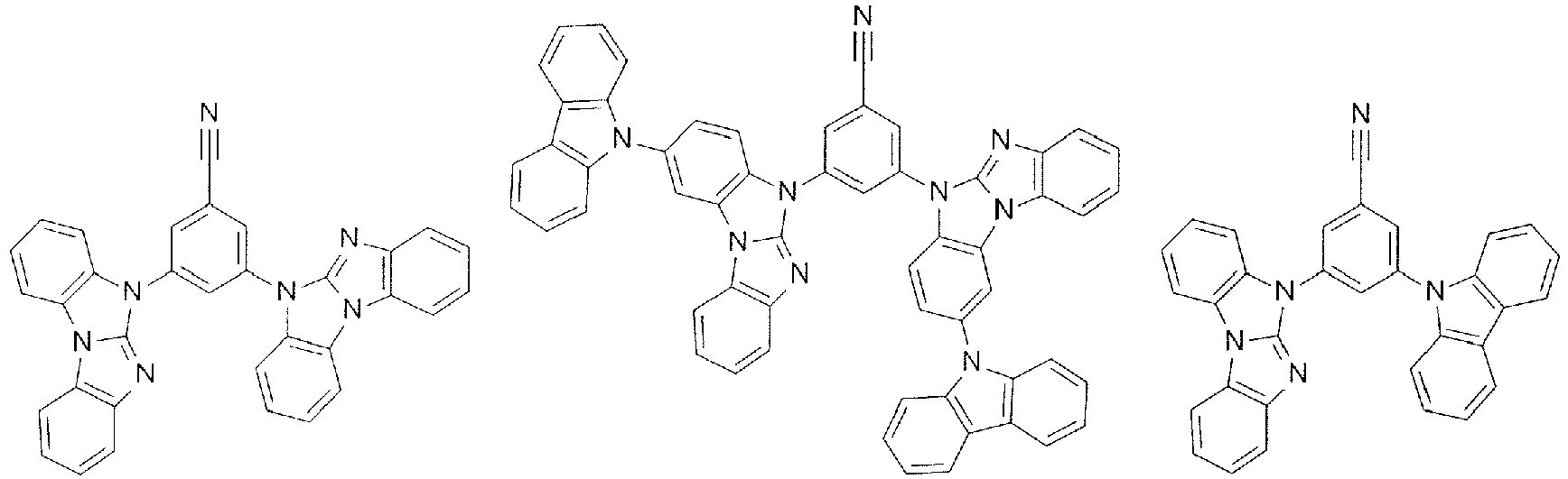
- Examples for compounds of formula Ib particularly suitable as TADF host material, especially for TADF based OLEDs emitting in the blue or green area of the visible electromagnetic spectrum:
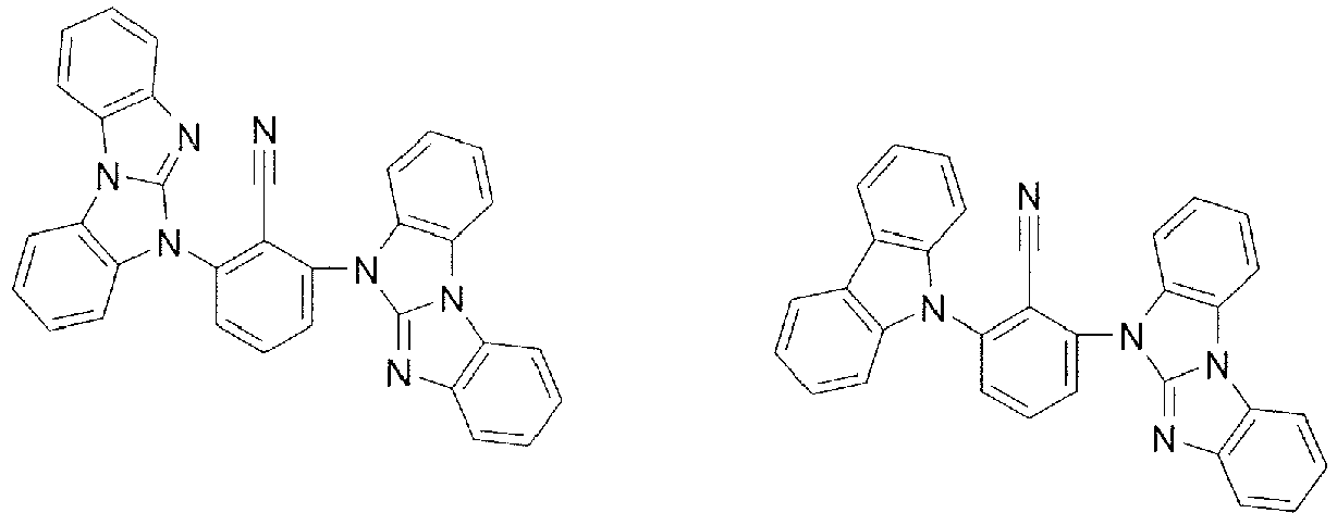
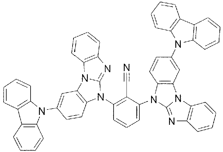
- The inventive organic light-emitting diode (OLED) thus generally has the following structure: an anode (a) and a cathode (i) and a light-emitting layer (e) arranged between the anode (a) and the cathode (i).
- The inventive OLED may, for example - in a preferred embodiment - be formed from the following layers:
- 1. Anode (a)
- 2. Hole transport layer (c)
- 3. Light-emitting layer (e)
- 4. Blocking layer for holes/excitons (f)
- 5. Electron transport layer (g)
- 6. Cathode (i)
- Layer sequences different than the aforementioned structure are also possible, and are known to those skilled in the art. For example, it is possible that the OLED does not have all of the layers mentioned; for example, an OLED with layers (a) (anode), (e) (light-emitting layer) and (i) (cathode) is likewise suitable, in which case the functions of the layers (c) (hole transport layer) and (f) (blocking layer for holes/excitons) and (g) (electron transport layer) are assumed by the adjacent layers. OLEDs which have layers (a), (c), (e) and (i), or layers (a), (e), (f), (g) and (i), are likewise suitable. In addition, the OLEDs may have a blocking layer for electrons/excitons (d) between the hole transport layer (c) and the Light-emitting layer (e).
- It is additionally possible that a plurality of the aforementioned functions (electron/exciton blocker, hole/exciton blocker, hole injection, hole conduction, electron injection, electron conduction) are combined in one layer and are assumed, for example, by a single material present in this layer. For example, a material used in the hole transport layer, in one embodiment, may simultaneously block excitons and/or electrons.
- Furthermore, the individual layers of the OLED among those specified above may in turn be formed from two or more layers. For example, the hole transport layer may be formed from a layer into which holes are injected from the electrode, and a layer which transports the holes away from the hole-injecting layer into the light-emitting layer. The electron transport layer may likewise consist of a plurality of layers, for example a layer in which electrons are injected by the electrode, and a layer which receives electrons from the electron injection layer and transports them into the light-emitting layer. These layers mentioned are each selected according to factors such as energy level, thermal resistance and charge carrier mobility, and also energy difference of the layers specified with the organic layers or the metal electrodes. The person skilled in the art is capable of selecting the structure of the OLEDs such that it is matched optimally to the organic compounds used in accordance with the invention.
- In a preferred embodiment the OLED according to the present invention comprises in this order:
- (a) an anode,
- (b) optionally a hole injection layer,
- (c) optionally a hole transport layer,
- (d) optionally an exciton blocking layer
- (e) an emitting layer,
- (f) optionally a hole/ exciton blocking layer
- (g) optionally an electron transport layer,
- (h) optionally an electron injection layer, and
- (i) a cathode.
- In a particularly preferred embodiment the OLED according to the present invention comprises in this order:
- (a) an anode,
- (b) optionally a hole injection layer,
- (c) a hole transport layer,
- (d) an exciton blocking layer
- (e) an emitting layer,
- (f) a hole/ exciton blocking layer
- (g) an electron transport layer, and
- (h) optionally an electron injection layer, and
- (i) a cathode.
- The properties and functions of these various layers, as well as example materials are known from the prior art and are described in more detail below on basis of preferred embodiments.
- The anode is an electrode which provides positive charge carriers. It may be composed, for example, of materials which comprise a metal, a mixture of different metals, a metal alloy, a metal oxide or a mixture of different metal oxides. Alternatively, the anode may be a conductive polymer. Suitable metals comprise the metals of groups 11, 4, 5 and 6 of the Periodic Table of the Elements, and also the transition metals of groups 8 to 10. When the anode is to be transparent, mixed metal oxides of groups 12, 13 and 14 of the Periodic Table of the Elements are generally used, for example indium tin oxide (ITO). It is likewise possible that the anode (a) comprises an organic material, for example polyaniline, as described, for example, in Nature, Vol. 357, pages 477 to 479 (June 11, 1992). Preferred anode materials include conductive metal oxides, such as indium tin oxide (ITO) and indium zinc oxide (IZO), aluminum zinc oxide (AlZnO), and metals. Anode (and substrate) may be sufficiently transparent to create a bottom-emitting device. A preferred transparent substrate and anode combination is commercially available ITO (anode) deposited on glass or plastic (substrate). A reflective anode may be preferred for some top-emitting devices, to increase the amount of light emitted from the top of the device. At least either the anode or the cathode should be at least partly transparent in order to be able to emit the light formed. Other anode materials and structures may be used.
- Generally, injection layers are comprised of a material that may improve the injection of charge carriers from one layer, such as an electrode or a charge generating layer, into an adjacent organic layer. Injection layers may also perform a charge transport function. The hole injection layer may be any layer that improves the injection of holes from anode into an adjacent organic layer. A hole injection layer may comprise a solution deposited material, such as a spin-coated polymer, or it may be a vapor deposited small molecule material, such as, for example, CuPc or MTDATA. Polymeric hole-injection materials can be used such as poly(N-vinylcarbazole) (PVK), polythiophenes, polypyrrole, polyaniline, self-doping polymers, such as, for example, sulfonated poly(thiophene-3-[2[(2-methoxyethoxy)ethoxy]-2,5-diyl) (Plexcore® OC Conducting Inks commercially available from Plextronics), and copolymers such as poly(3,4-ethylenedioxythiophene)/poly(4-styrenesulfonate) also called PEDOT/PSS.
- Either hole-transporting molecules or polymers may be used as the hole transport material. Suitable hole transport materials for layer (c) of the inventive OLED are disclosed, for example, in Kirk-Othmer Encyclopedia of Chemical Technology, 4th Edition, Vol. 18, pages 837 to 860, 1996,
US20070278938 ,US2008/0106190 ,US2011/0163302 (triarylamines with (di)benzothiophen/(di)benzofuran; Nan-Xing Hu et al. Synth. Met. 111 (2000) 421 (indolocarbazoles),WO2010002850 (substituted phenylamine compounds) andWO2012/16601 WO2012/16601 WO2013/022419 , wherein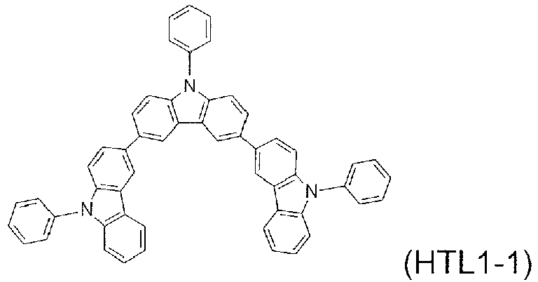

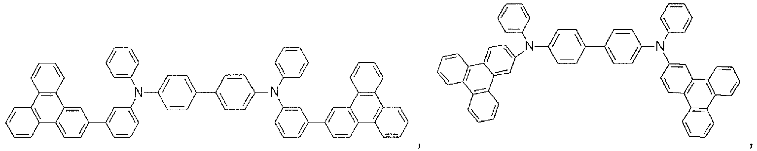

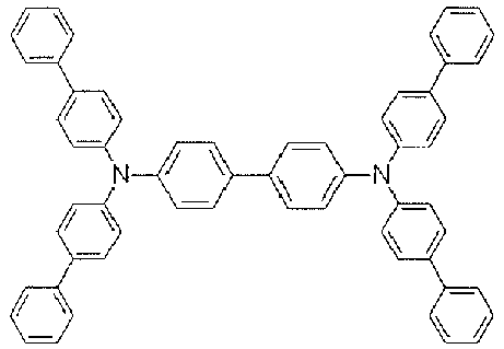

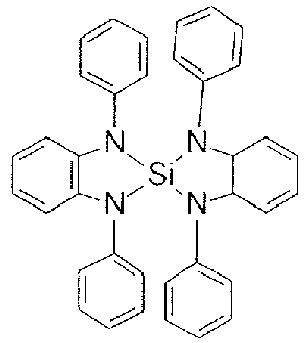
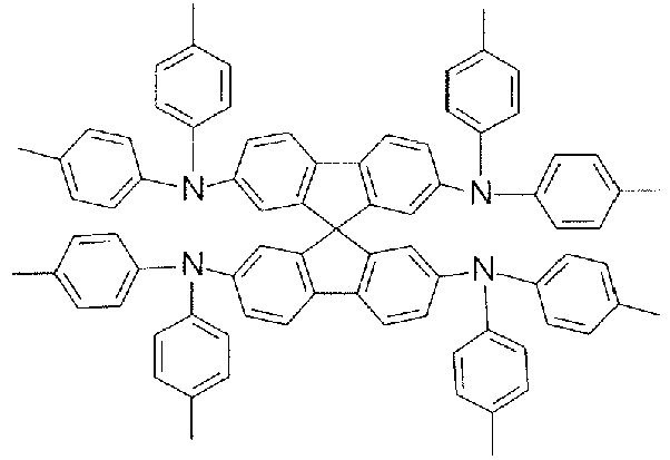
- In a preferred embodiment it is possible to use metal carbene complexes as hole transport materials. Suitable carbene complexes are, for example, carbene complexes as described in
WO2005/019373A2 ,WO2006/056418 A2 ,WO2005/113704 ,WO2007/115970 ,WO2007/115981 ,WO2008/000727 andPCT/EP2014/055520 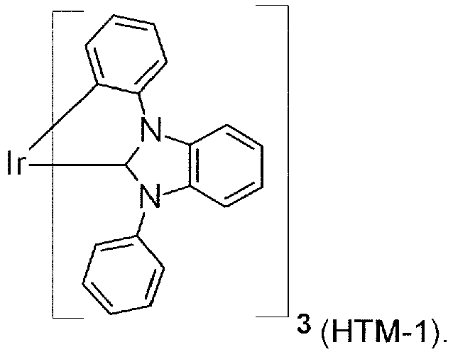
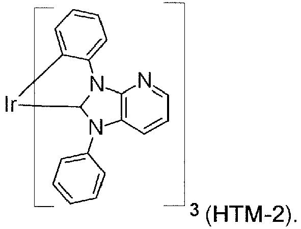
- The hole-transporting layer may also be electronically doped in order to improve the transport properties of the materials used, in order firstly to make the layer thicknesses more generous (avoidance of pinholes/short circuits) and in order secondly to minimize the operating voltage of the device. Electronic doping is known to those skilled in the art and is disclosed, for example, in W. Gao, A. Kahn, J. Appl. Phys., Vol. 94, 2003, 359 (p-doped organic layers); A. G. Werner, F. Li, K. Harada, M. Pfeiffer, T. Fritz, K. Leo, Appl. Phys. Lett., Vol. 82, No. 25, 2003, 4495 and Pfeiffer et al., Organic Electronics 2003, 4, 89 - 103 and K. Walzer, B. Maennig, M. Pfeiffer, K. Leo, Chem. Soc. Rev. 2007, 107, 1233. For example it is possible to use mixtures in the hole-transporting layer, in particular mixtures which lead to electrical p-doping of the hole-transporting layer. p-Doping is achieved by the addition of oxidizing materials. These mixtures may, for example, be the following mixtures: mixtures of the abovementioned hole transport materials with at least one metal oxide, for example MoO2, MoO3, WOx, ReO3 and/or V2O5, preferably MoO3 and/or ReO3, more preferably MoO3, or mixtures comprising the aforementioned hole transport materials and one or more compounds selected from 7,7,8,8-tetracyanoquinodimethane (TCNQ), 2,3,5,6-tetrafluoro-7,7,8,8-tetracyanoquinodimethane (F4-TCNQ), 2,5-bis(2-hydroxyethoxy)-7,7,8,8-tetracyanoquinodimethane, bis(tetra-n-butylammonium)tetracyanodiphenoquinodimethane, 2,5-dimethyl-7,7,8,8-tetracyanoquinodimethane, tetracyanoethylene, 11,11,12,12-tetracyanonaphtho2,6-quinodimethane, 2-fluoro-7,7,8,8-tetracyanoquino-dimethane, 2,5-difluoro-7,7,8,8etracyanoquinodimethane, dicyanomethylene-1,3,4,5,7,8-hexafluoro-6Hnaphthalen-2-ylidene)malononitrile (F6-TNAP), Mo(tfd)3 (from Kahn et al., J. Am. Chem. Soc. 2009, 131 (35), 12530-12531), compounds as described in
EP1988587 ,US2008265216 ,EP2180029 ,US20100102709 ,WO2010132236 ,EP2180029 and quinone compounds as mentioned inEP2401254 . - Preferred mixtures comprise the aforementioned carbene complexes, such as, for example, the carbene complexes HTM-1 and HTM-2, and MoO3 and/or ReO3, especially MoO3. In a particularly preferred embodiment the hole transport layer comprises from 0.1 to 10 wt % of MoO3 and 90 to 99.9 wt % carbene complex, especially of the carbene complex HTM-1 and HTM-2, wherein the total amount of the MoO3 and the carbene complex is 100 wt %.
- Blocking layers may be used to reduce the number of charge carriers (electrons or holes) and/or excitons that leave the emissive layer. An electron/exciton blocking layer (d) may be disposed between the first emitting layer (e) and the hole transport layer (c), to block electrons from emitting layer (e) in the direction of hole transport layer (c). Blocking layers may also be used to block excitons from diffusing out of the emissive layer. Suitable metal complexes for use as electron/exciton blocker material are, for example, carbene complexes as described in
WO2005/019373A2 ,WO2006/056418A2 ,WO2005/113704 ,WO2007/115970 ,WO2007/115981 ,WO2008/000727 andPCT/EP2014/055520 - The light-emitting layer (e) comprises at least one emitter material. In principle, it may be a fluorescence or phosphorescence emitter, suitable emitter materials being known to those skilled in the art. The at least one emitter material is preferably a phosphorescence emitter. The phosphorescence emitter compounds used with preference are based on metal complexes, and especially the complexes of the metals Ru, Rh, Ir, Pd and Pt, in particular the complexes of Ir, have gained significance. The compounds of the formula Ib can be used as the matrix in the light-emitting layer.
- Suitable metal complexes for use in the inventive OLEDs, preferably as emitter material, are described, for example, in documents
WO 02/60910 A1 US 2001/0015432 A1 ,US 2001/0019782 A1 ,US 2002/0055014 A1 ,US 2002/0024293 A1 ,US 2002/0048689 A1 ,EP 1 191 612 A2 ,EP 1 191 613 A2 ,EP 1 211 257 A2 ,US 2002/0094453 A1 ,WO 02/02714 A2 WO 00/70655 A2 WO 01/41512 A1 WO 02/15645 A1 WO 2005/019373 A2 ,WO 2005/113704 A2 ,WO 2006/115301 A1 ,WO 2006/067074 A1 ,WO 2006/056418 ,WO 2006121811 A1 ,WO 2007095118 A2 ,WO 2007/115970 ,WO 2007/115981 ,WO 2008/000727 ,WO2010129323 ,WO2010056669 ,WO10086089 US2011/0057559 ,WO2011/106344 ,US2011/0233528 ,WO2012/048266 andWO2012/172482 . - Further suitable metal complexes are the commercially available metal complexes tris(2-phenylpyridine)iridium(III), iridium(III) tris(2-(4-tolyl)pyridinato-N,C2'), bis(2-phenylpyridine)(acetylacetonato)iridium(III), iridium(III) tris(1-phenylisoquinoline), iridium(III) bis(2,2'-benzothienyl)pyridinato-N,C3')(acetylacetonate), tris(2-phenylquinoline)iridium(III), iridium(III) bis(2-(4,6-difluorophenyl)pyridinato-N,C2)picolinate, iridium(III) bis(1-phenylisoquinoline)(acetylacetonate), bis(2-phenylquinoline)(acetylacetonato)iridium(III), iridium(III) bis(di-benzo[f,h]quinoxaline)(acetylacetonate), iridium(III) bis(2-methyldibenzo[f,h]quinoxaline)(acetylacetonate) and tris(3-methyl-1-phenyl-4-trimethylacetyl-5-pyrazolino)terbium(III), bis[1-(9,9-dimethyl-9H-fluoren-2-yl)isoquinoline](acetylacetonato)iridium(III), bis(2-phenylbenzothiazolato)(acetylacetonato)iridium(III), bis(2-(9,9-dihexylfluorenyl)-1-pyridine)(acetylacetonato)iridium(III), bis(2-benzo[b]thiophen-2-ylpyridine)(acetylacetonato)iridium(III).
- In addition, the following commercially available materials are suitable:
tris(dibenzoylacetonato)mono(phenanthroline)europium(III), tris(dibenzoylmethane)-mono(phenanthroline)europium(III), tris(dibenzoylmethane)mono(5-aminophenanthroline)-europium(III), tris(di-2-naphthoylmethane)mono(phenanthroline)europium(III), tris(4-bromobenzoylmethane)mono(phenanthroline)europium(III), tris(di(biphenyl)methane)-mono(phenanthroline)europium(III), tris(dibenzoylmethane)mono(4,7-diphenyl-phenanthroline)europium(III), tris(dibenzoylmethane)mono(4,7-di-methyl-phenanthroline)europium(III), tris(dibenzoylmethane)mono(4,7-dimethylphenanthrolinedisulfonic acid)europium(III) disodium salt, tris[di(4-(2-(2-ethoxyethoxy)ethoxy)benzoylmethane)]mono-(phenanthroline)europium(III) and tris[di[4-(2-(2-ethoxyethoxy)ethoxy)benzoylmethane)]mono(5-aminophenanthroline)europium(III), osmium(II) bis(3-(trifluoromethyl)-5-(4-tert-butylpyridyl)-1,2,4-triazolato)diphenylmethylphosphine, osmium(II) bis(3-(trifluoromethyl)-5-(2-pyridyl)-1,2,4-triazole)dimethylphenylphosphine, osmium(II) bis(3-(trifluoromethyl)-5-(4-tert-butylpyridyl)-1,2,4-triazolato)dimethylphenylphosphine, osmium(II) bis(3-(trifluoromethyl)-5-(2-pyridyl)-pyrazolato)dimethylphenylphosphine, tris[4,4'-di-tert-butyl(2,2')-bipyridine]ruthenium(III), osmium(II) bis(2-(9,9-dibutylfluorenyl)-1-isoquinoline(acetylacetonate). - Preferred phosphorescence emitters are carbene complexes.
- Suitable phosphorescent blue emitters are specified in the following publications:
WO2006/056418A2 ,WO2005/113704 ,WO2007/115970 ,WO2007/115981 ,WO2008/000727 ,WO2009050281 ,WO2009050290 ,WO2011051404 ,US2011/057559 WO2011/073149 ,WO2012/121936A2 ,US2012/0305894A1 ,WO2012/170571 ,WO2012/170461 ,WO2012/170463 ,WO2006/121811 ,WO2007/095118 ,WO2008/156879 ,WO2008/156879 ,WO2010/068876 ,US2011/0057559 ,WO2011/106344 ,US2011/0233528 ,WO2012/048266 ,WO2012/172482 ,PCT/EP2014/064054 PCT/EP2014/066272 - Preferably, the light emitting layer (e) comprises at least one carbene complex as phosphorescence emitter. Suitable carbene complexes are, for example, compounds of the formula

WO 2005/019373 A2 , wherein the symbols have the following meanings: - M is a metal atom selected from the group consisting of Co, Rh, Ir, Nb, Pd, Pt, Fe, Ru, Os, Cr, Mo, W, Mn, Tc, Re, Cu, Ag and Au in any oxidation state possible for the respective metal atom;
- carbene is a carbene ligand which may be uncharged or monoanionic and monodentate, bidentate or tridentate, with the carbene ligand also being able to be a biscarbene or triscarbene ligand;
- L is a monoanionic or dianionic ligand, which may be monodentate or bidentate;
- K is an uncharged monodentate or bidentate ligand, preferably selected from the group consisting of phosphines; phosphonates and derivatives thereof, arsenates and derivatives thereof; phosphites; CO; pyridines; nitriles and conjugated dienes which form a π complex with M1;
- n1 is the number of carbene ligands, where n1 is at least 1 and when n1 > 1 the carbene ligands in the complex of the formula Ib can be identical or different;
- m1 is the number of ligands L, where m1 can be 0 or ≥ 1 and when m1 > 1 the ligands L can be identical or different;
- o is the number of ligands K, where o can be 0 or ≥ 1 and when o > 1 the ligands K can be identical or different;
- where the sum n1 + m1 + o is dependent on the oxidation state and coordination number of the metal atom and on the denticity of the ligands carbene, L and K and also on the charge on the ligands, carbene and L, with the proviso that n1 is at least 1.
- More preferred are metal-carbene complexes of the general formula
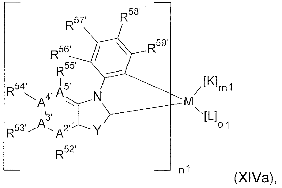
WO2011/073149 where M is Ir, or Pt, - n1 is an integer selected from 1, 2 and 3,
- Y is NR51', O, S or C(R25')2,
- A2', A3', A4', and A5' are each independently N or C, where 2 A' = nitrogen atoms and at least one carbon atom is present between two nitrogen atoms in the ring,
- R51' is a linear or branched alkyl radical optionally interrupted by at least one heteroatom, optionally bearing at least one functional group and having 1 to 20 carbon atoms, cycloalkyl radical optionally interrupted by at least one heteroatom, optionally bearing at least one functional group and having 3 to 20 carbon atoms, substituted or unsubstituted aryl radical optionally interrupted by at least one heteroatom, optionally bearing at least one functional group and having 6 to 30 carbon atoms, substituted or unsubstituted heteroaryl radical optionally interrupted by at least one heteroatom, optionally bearing at least one functional group and having a total of 5 to 18 carbon atoms and/or heteroatoms,
- R52', R53', R54' and R55' are each, if A2', A3', A4' and/or A5' is N, a free electron pair, or, if A2', A3', A4' and/or A5' is C, each independently hydrogen, linear or branched alkyl radical optionally interrupted by at least one heteroatom, optionally bearing at least one functional group and having 1 to 20 carbon atoms, cycloalkyl radical optionally interrupted by at least one heteroatom, optionally bearing at least one functional group and having 3 to 20 carbon atoms, substituted or unsubstituted aryl radical optionally interrupted by at least one heteroatom, optionally bearing at least one functional group and having 6 to 30 carbon atoms, substituted or unsubstituted heteroaryl radical optionally interrupted by at least one heteroatom, optionally bearing at least one functional group and having a total of 5 to 18 carbon atoms and/or heteroatoms, group with donor or acceptor action, or
- R53' and R54' together with A3' and A4' form an optionally substituted, unsaturated ring optionally interrupted by at least one further heteroatom and having a total of 5 to 18 carbon atoms and/or heteroatoms,
- R56', R57', R58' and R59' are each independently hydrogen, linear or branched alkyl radical optionally interrupted by at least one heteroatom, optionally bearing at least one functional group and having 1 to 20 carbon atoms, cycloalkyl radical optionally interrupted by at least one heteroatom, optionally bearing at least one functional group and having 3 to 20 carbon atoms, cyclo-heteroalkyl radical optionally interrupted by at least one heteroatom, optionally bearing at least one functional group and having 3 to 20 carbon atoms, substituted or unsubstituted aryl radical optionally interrupted by at least one heteroatom, optionally bearing at least one functional group and having 6 to 30 carbon atoms, substituted or unsubstituted heteroaryl radical optional-ly interrupted by at least one heteroatom, optionally bearing at least one functional group and having a total of 5 to 18 carbon atoms and/or heteroatoms, group with donor or acceptor action, or
- R56' and R57', R57' and R58' or R58' and R59', together with the carbon atoms to which they are bonded, form a saturated, unsaturated or aromatic, optionally substituted ring optionally interrupted by at least one heteroatom and having a total of 5 to 18 carbon atoms and/or heteroatoms, and/or
- if A5' is C, R55' and R56' together form a saturated or unsaturated, linear or branched bridge optionally comprising heteroatoms, an aromatic unit, heteroaromatic unit and/or functional groups and having a total of 1 to 30 carbon atoms and/or heteroatoms, to which is optionally fused a substituted or unsubstituted, five- to eight-membered ring comprising carbon atoms and/or heteroatoms,
- R25' is independently a linear or branched alkyl radical optionally interrupted by at least one heteroatom, optionally bearing at least one functional group and having 1 to 20 carbon atoms, cycloalkyl radical optionally interrupted by at least one heteroatom, optionally bearing at least one functional group and having 3 to 20 carbon atoms, substituted or unsubstituted aryl radical optionally interrupted by at least one heteroatom, optionally bearing at least one functional group and having 6 to 30 carbon atoms, substituted or unsubstituted heteroaryl radical optionally interrupted by at least one heteroatom, optionally bearing at least one functional group and having a total of 5 to 18 carbon atoms and/or heteroatoms,
- K is an uncharged mono- or bidentate ligand,
- L is a mono- or dianionic ligand, preferably monoanionic ligand, which may be mono- or bidentate,
- m1 is 0, 1 or 2, where, when m1 is 2, the K ligands may be the same or different,
- o1 is 0, 1 or 2, where, when o1 is 2, the L ligands may be the same or different.
- The compound of formula XIV is preferably a compound of the formula:
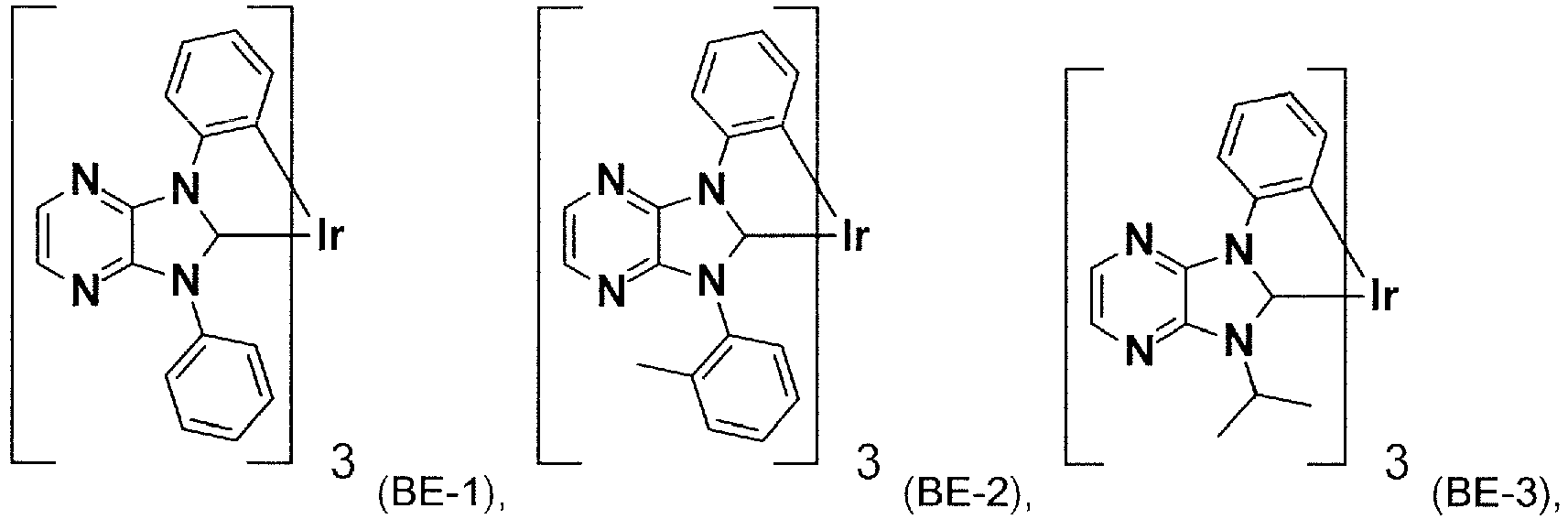
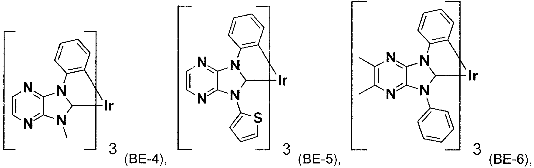
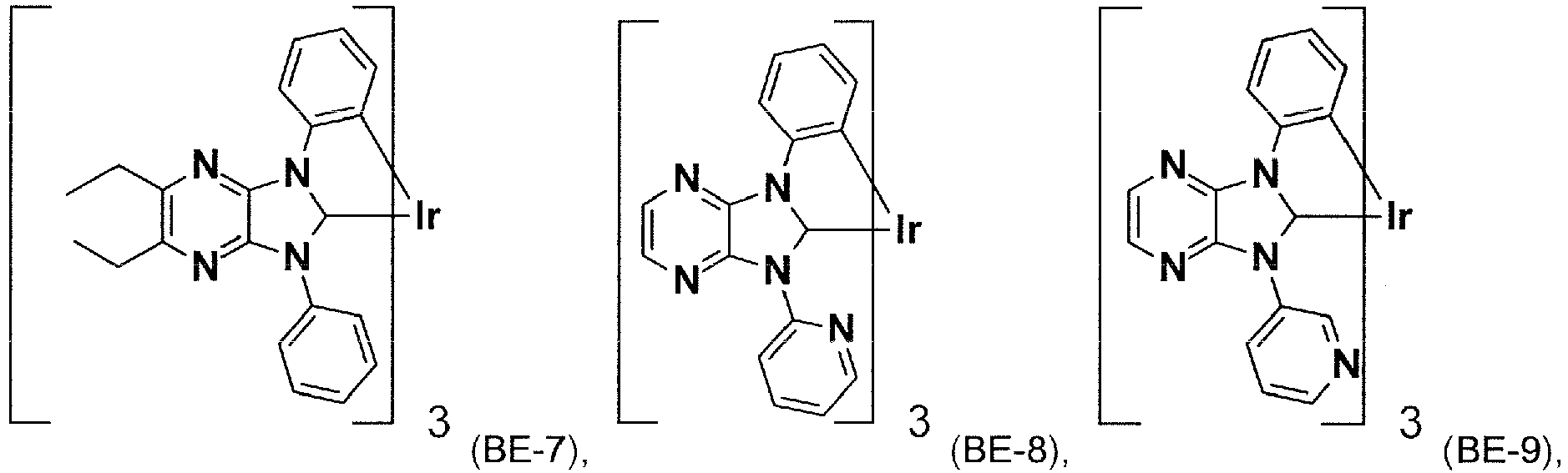
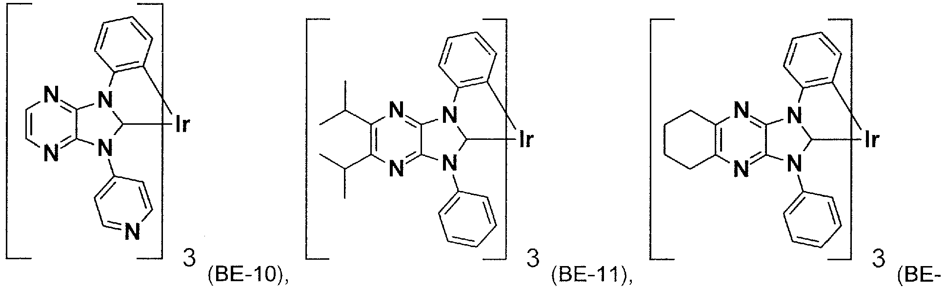

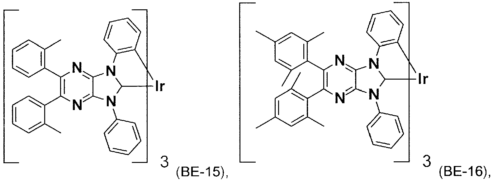


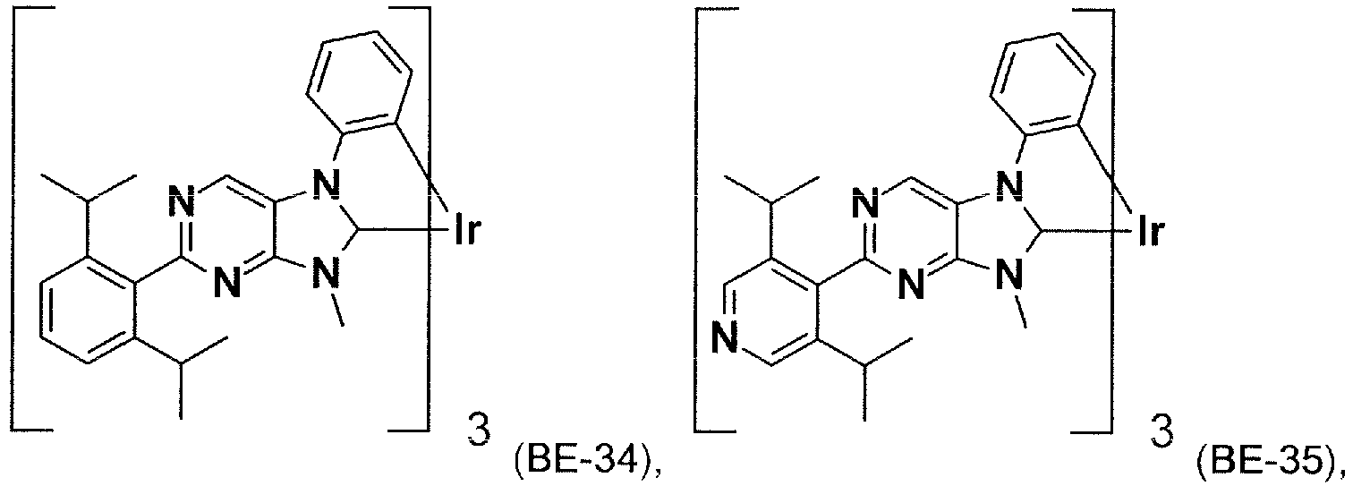
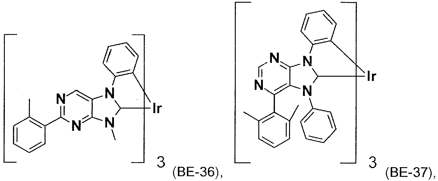
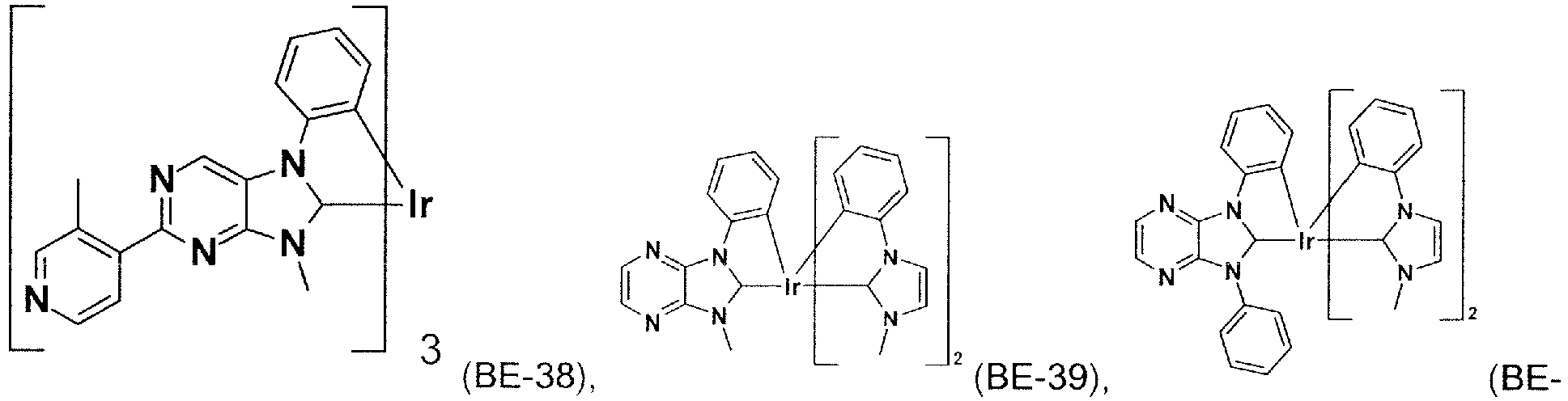

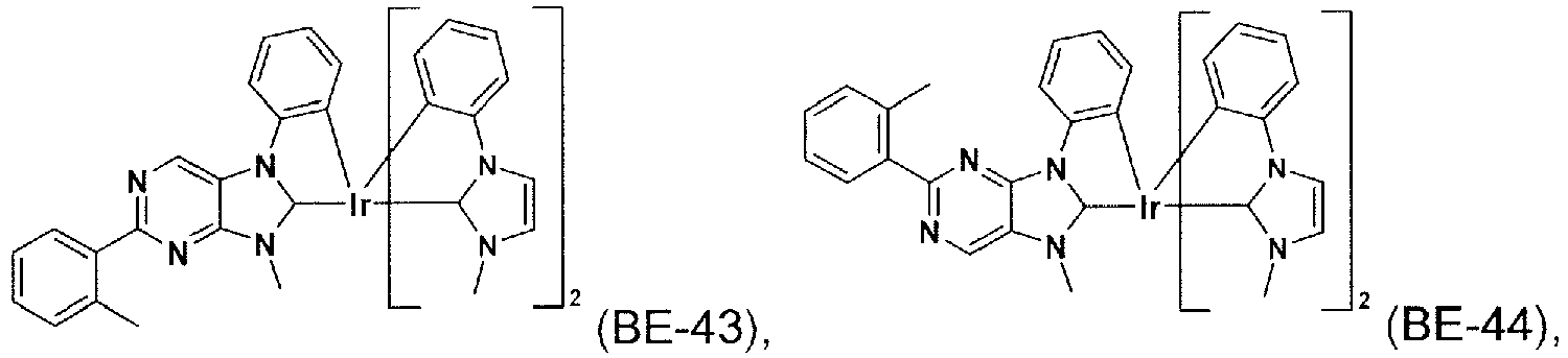
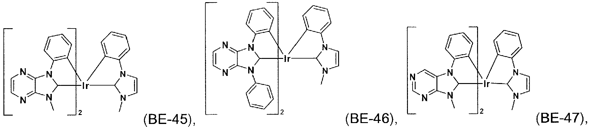
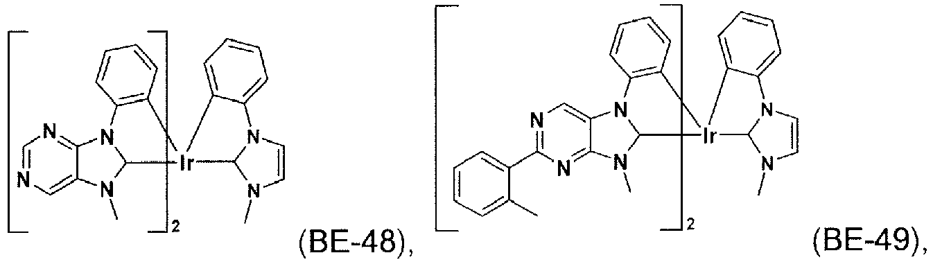
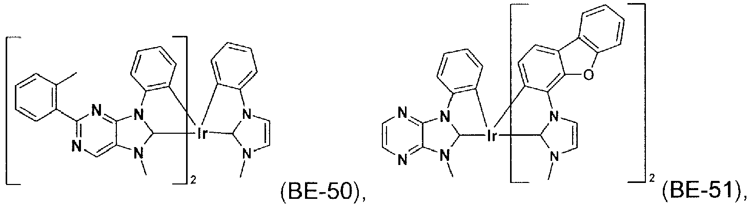

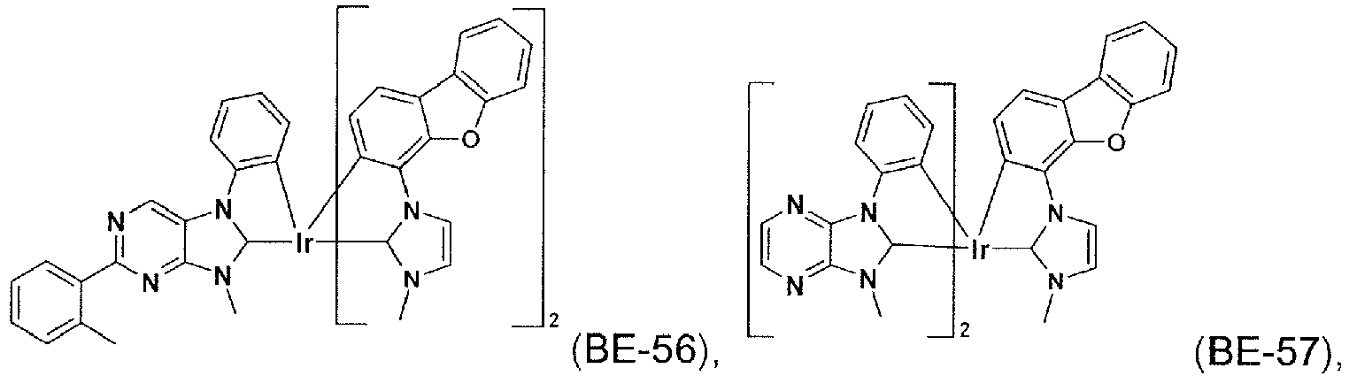


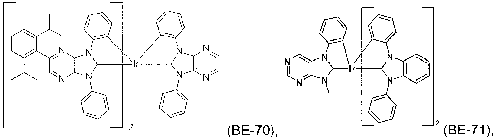

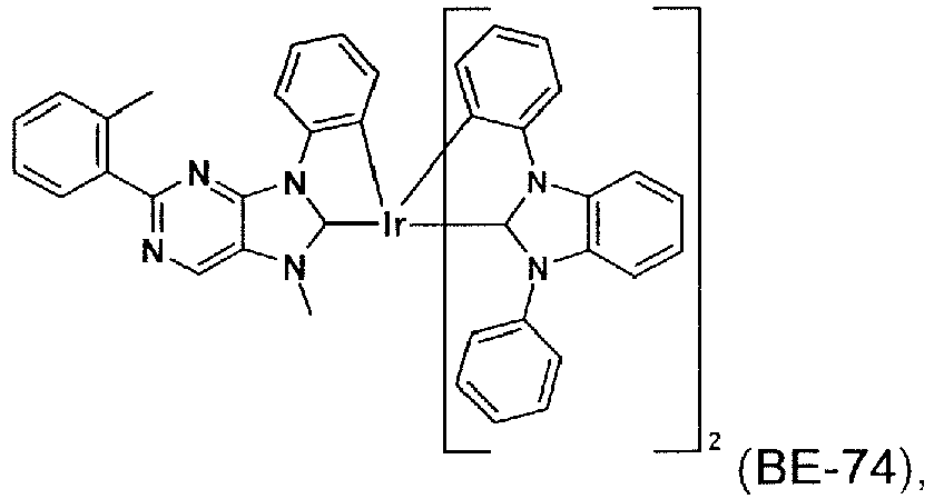
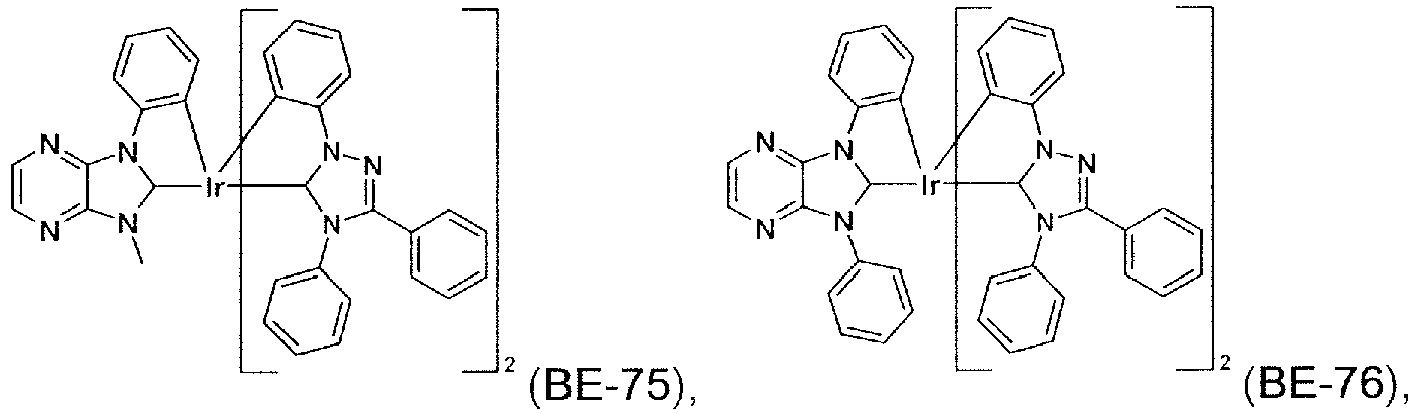

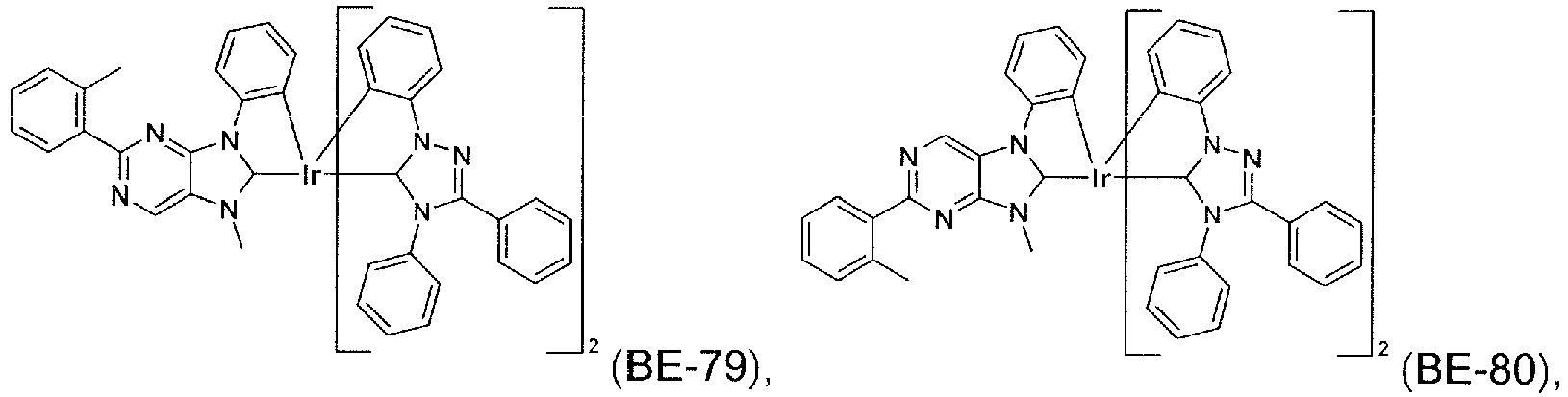
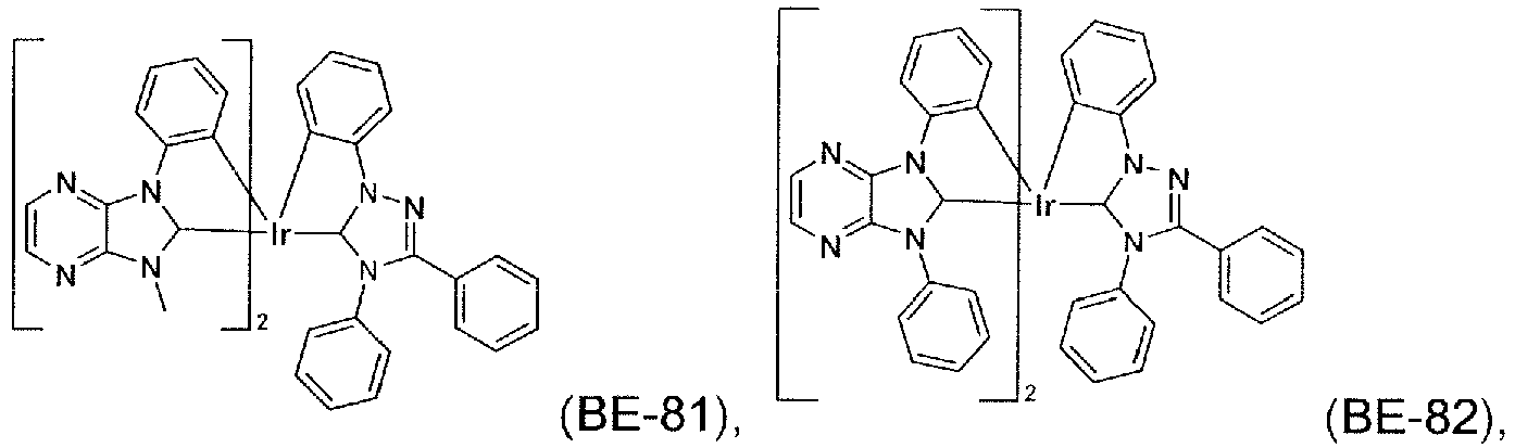
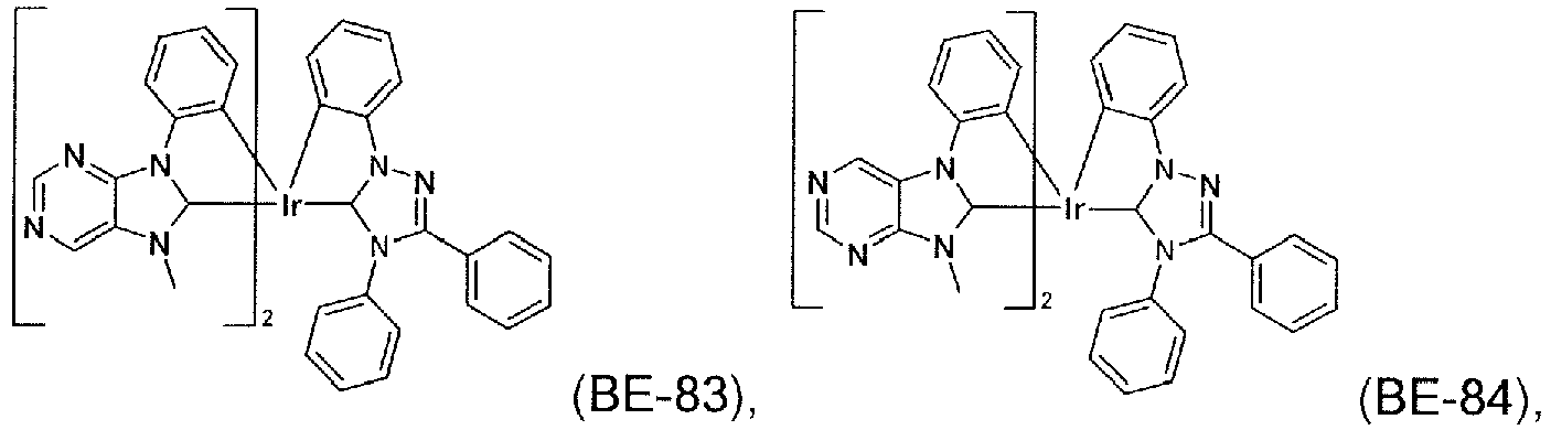
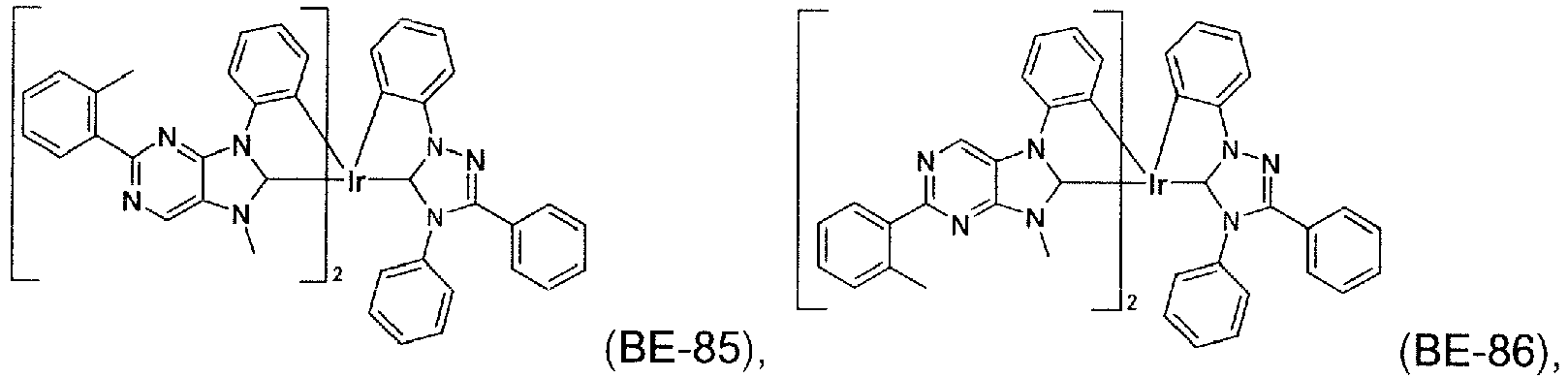
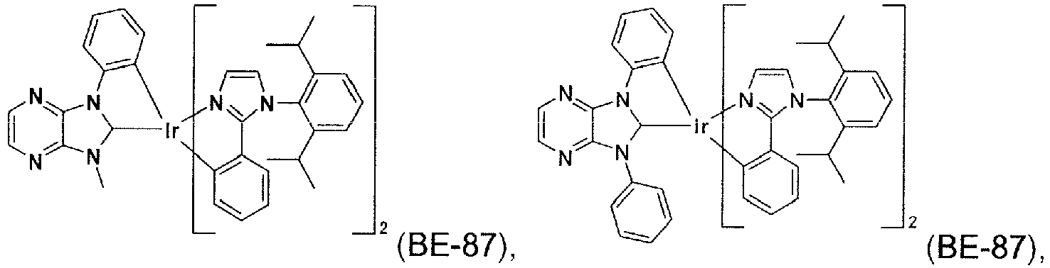
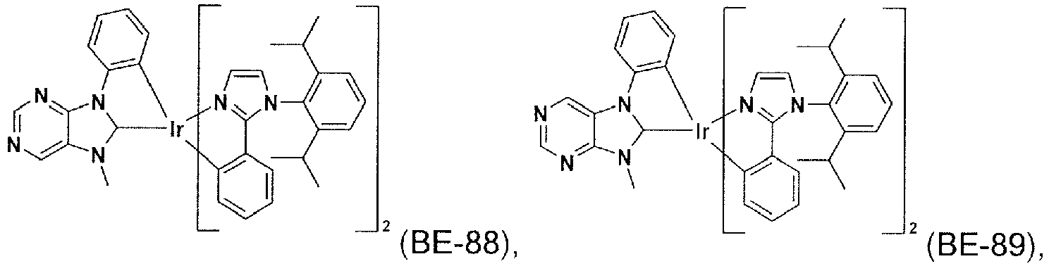


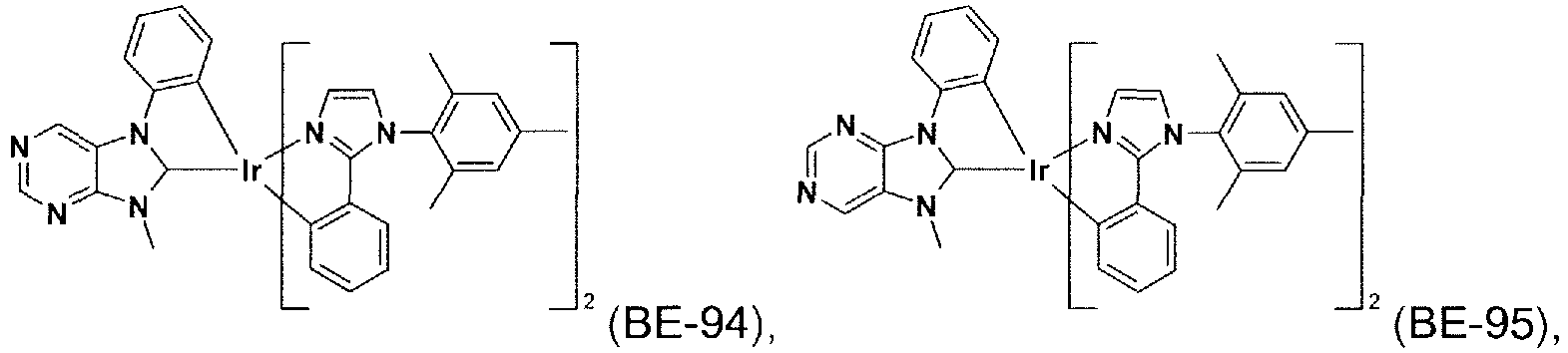

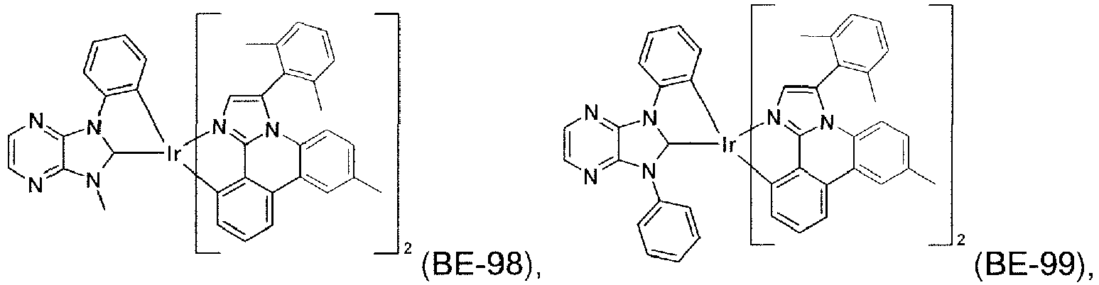
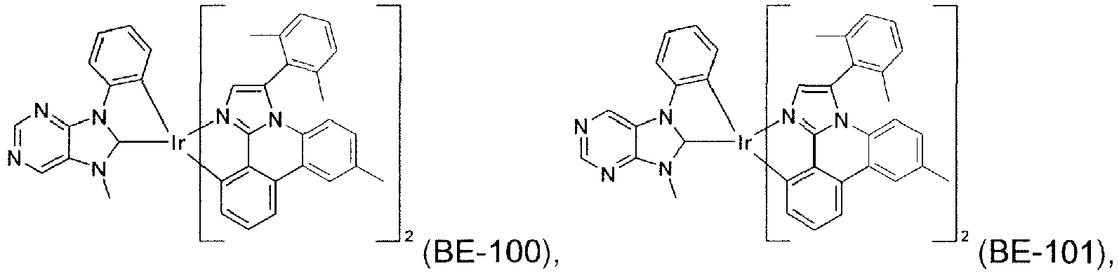
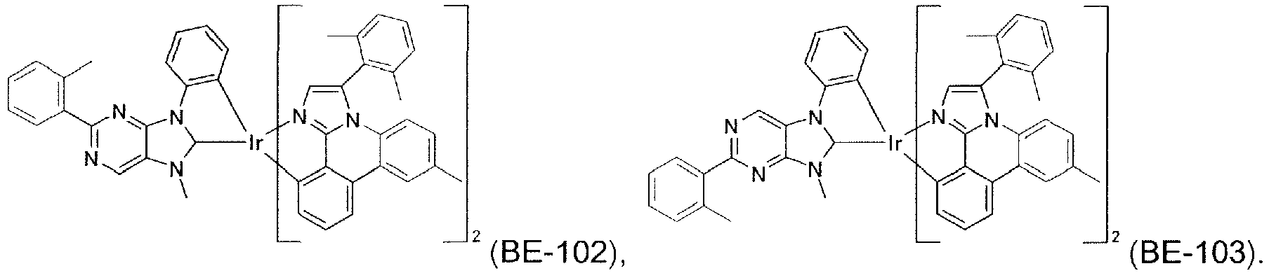
- Further suitable non-carbene emitter materials are mentioned below:

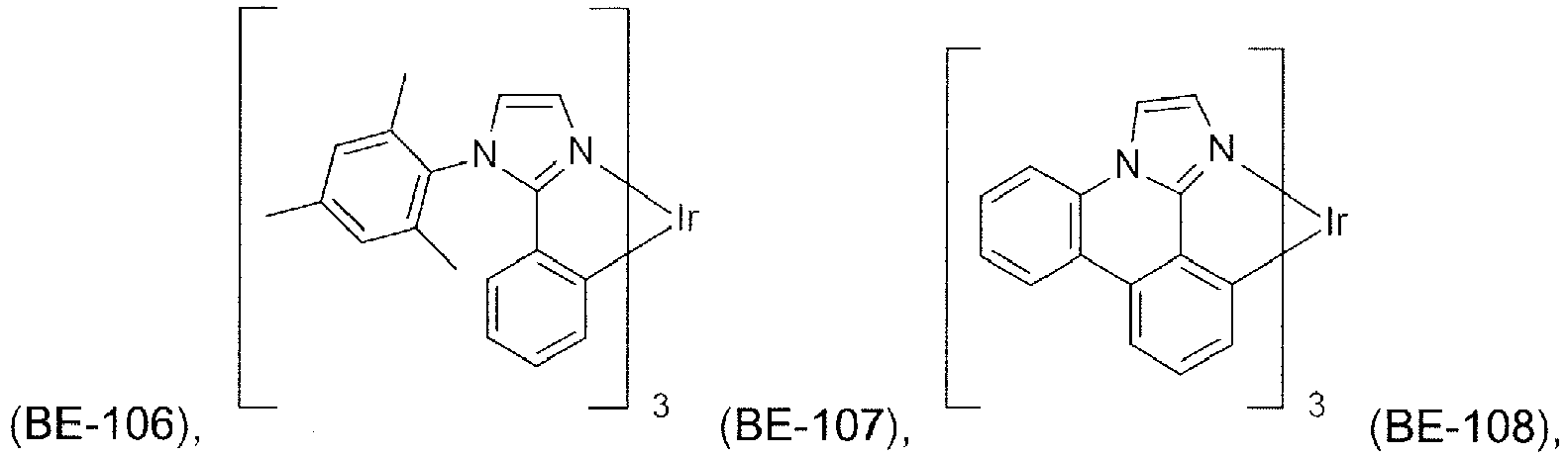
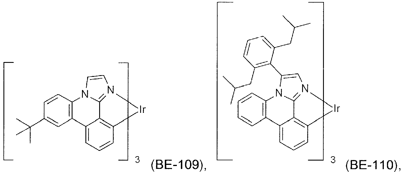
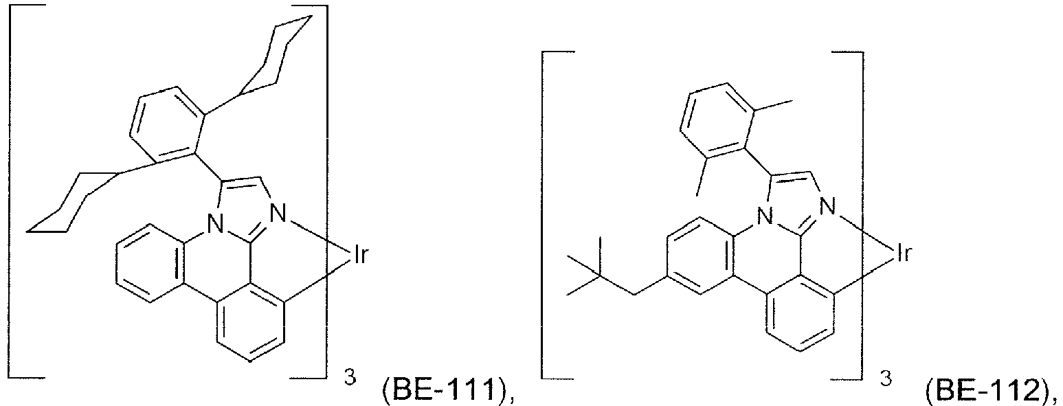
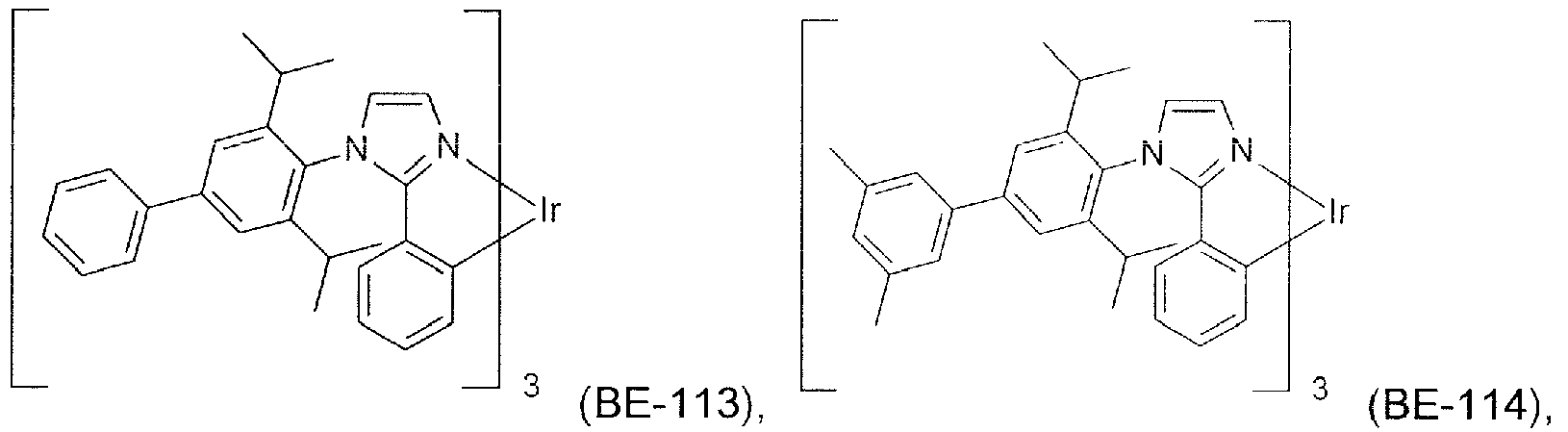
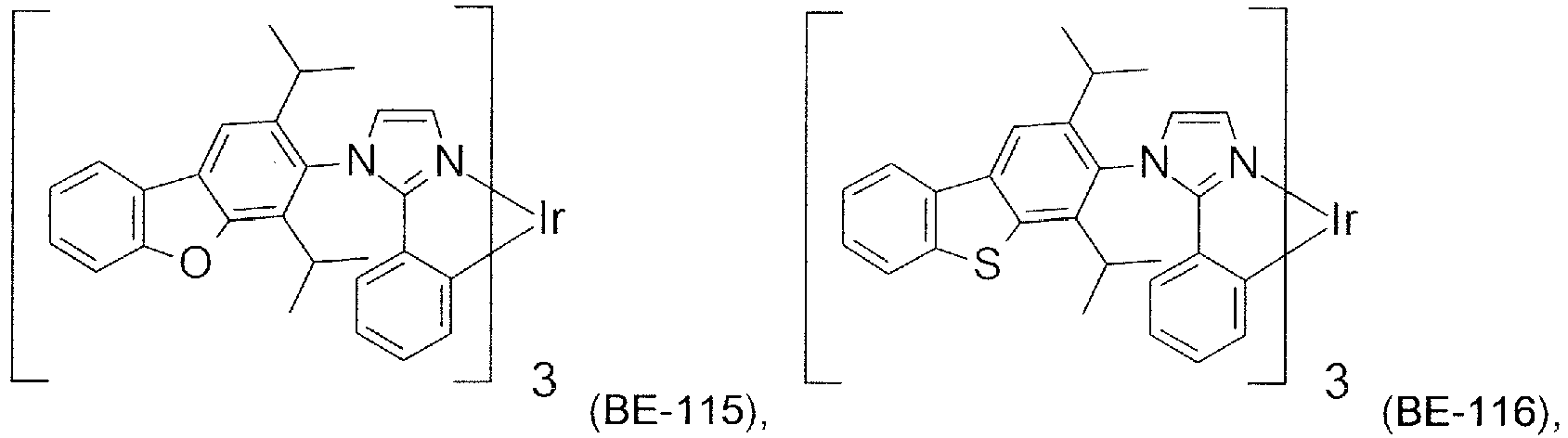
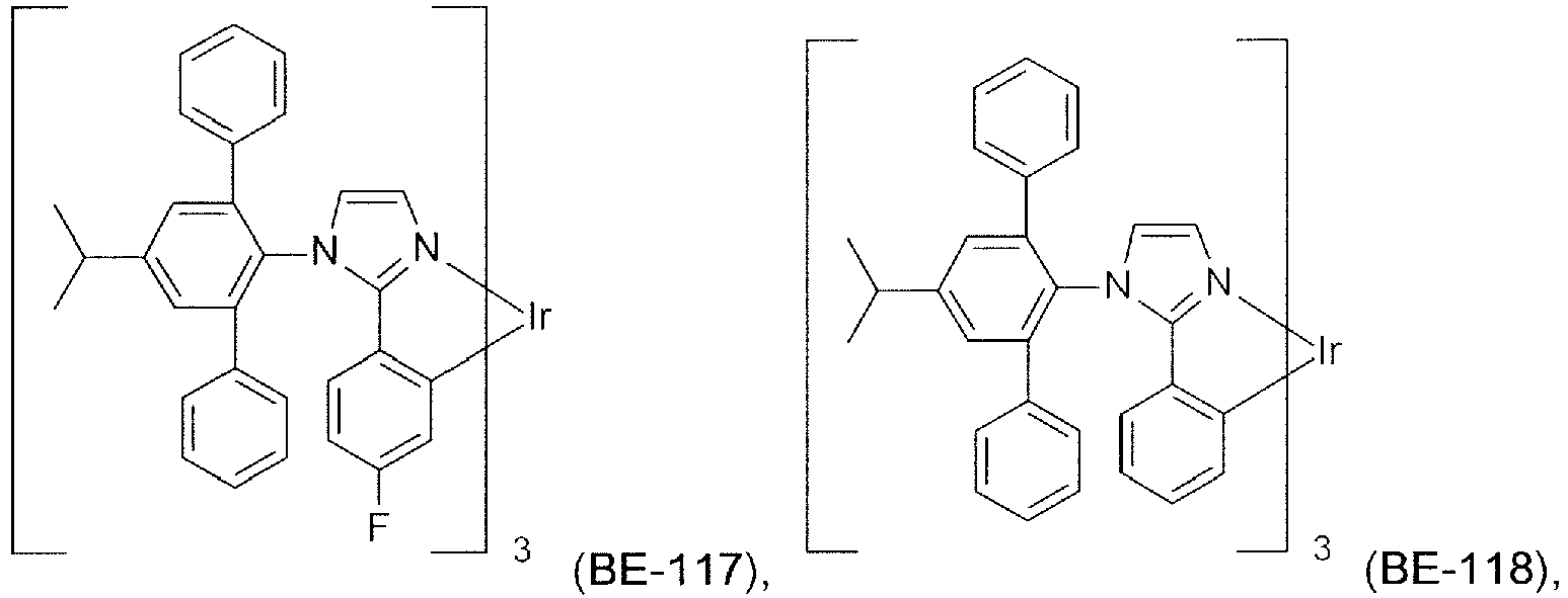
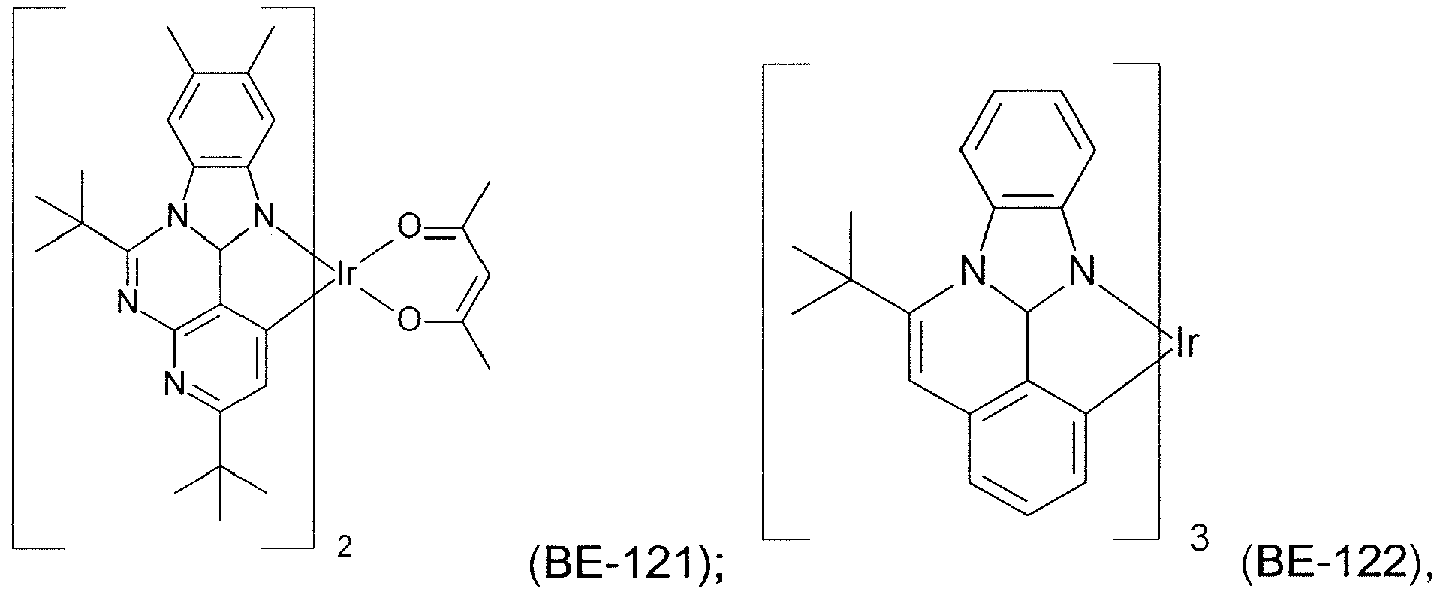
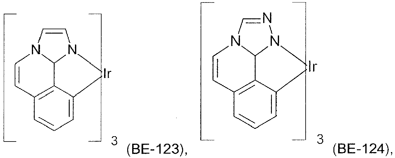
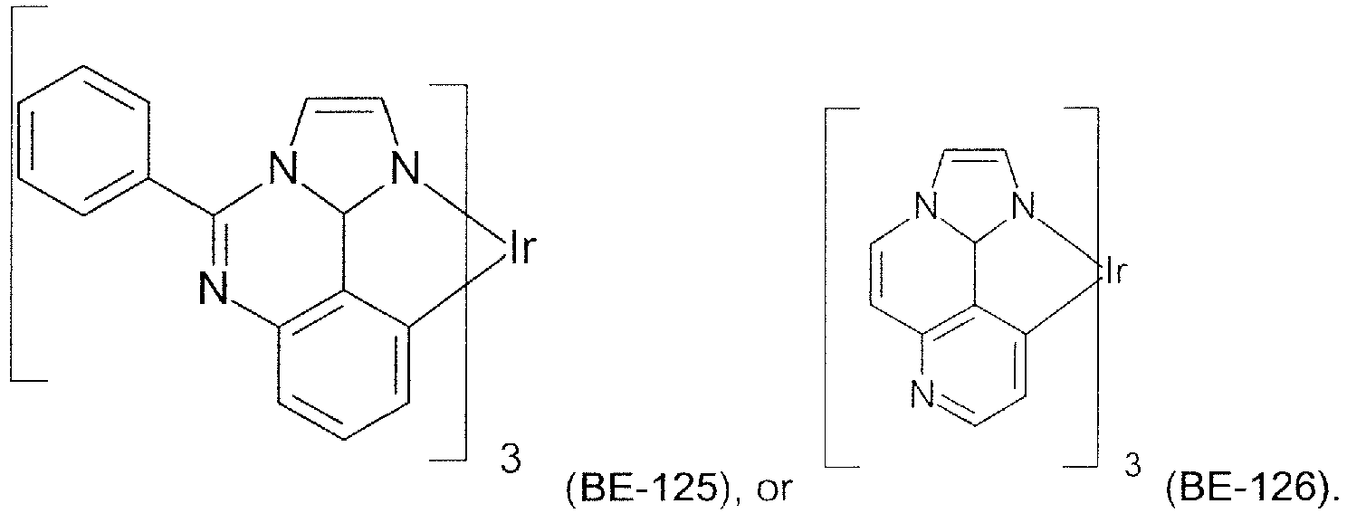
- The compound of formula XIV is more preferably a compound (BE-1), (BE-2), (BE-7), (BE-12), (BE-16), (BE-64), or (BE-70). The most preferred phosphorescent blue emitters are compounds (BE-1) and (BE-12).
- The homoleptic metal-carbene complexes may be present in the form of facial or meridional isomers or mixtures thereof, preference being given to the facial isomers.
- Suitable carbene complexes of formula (XIV) and their preparation process are, for example described in
WO2011/073149 . - The compounds of the present invention can also be used as host for phosphorescent green emitters. Suitable phosphorescent green emitters are, for example, specified in the following publications:
WO2006014599 ,WO20080220265 WO2009073245 ,WO2010027583 ,WO2010028151 ,US20110227049 ,WO2011090535 ,WO2012/08881 WO20100056669 WO20100118029 WO20100244004 WO2011109042 ,WO2012166608 ,US20120292600 ,EP2551933A1 ;US6687266 ,US20070190359 ,US20070190359 ,US20060008670 ;WO2006098460 ,US20110210316 ,WO2012053627 ;US6921915 ,US20090039776 ;JP2007123392 14180422.9 - Examples of suitable phosphorescent green emitters are shown below:
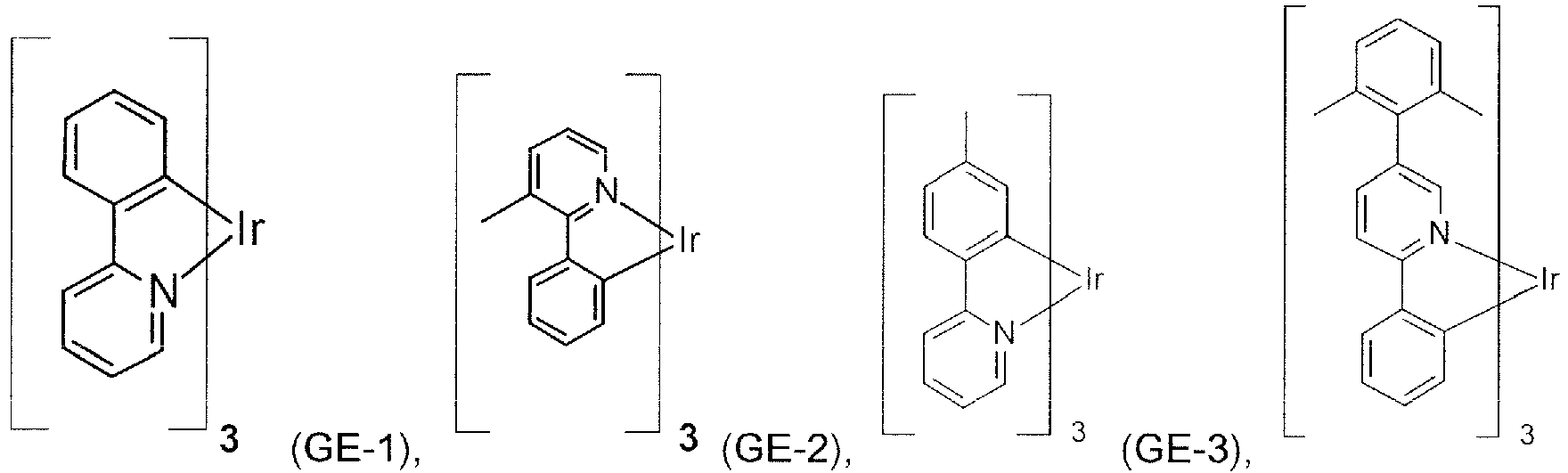
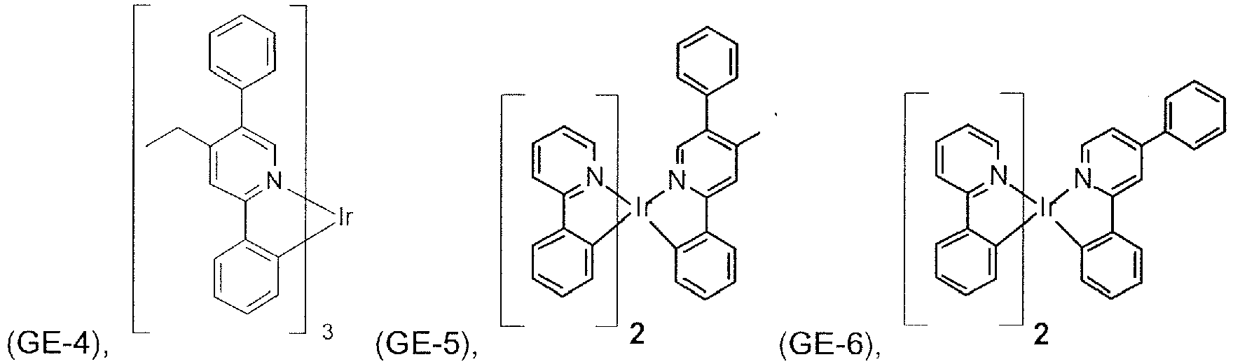
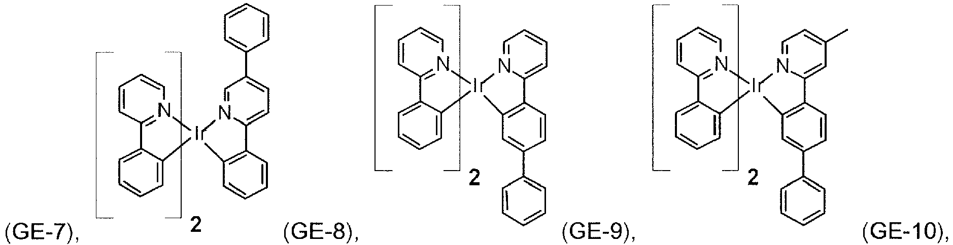
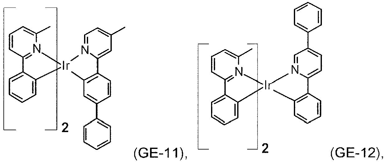


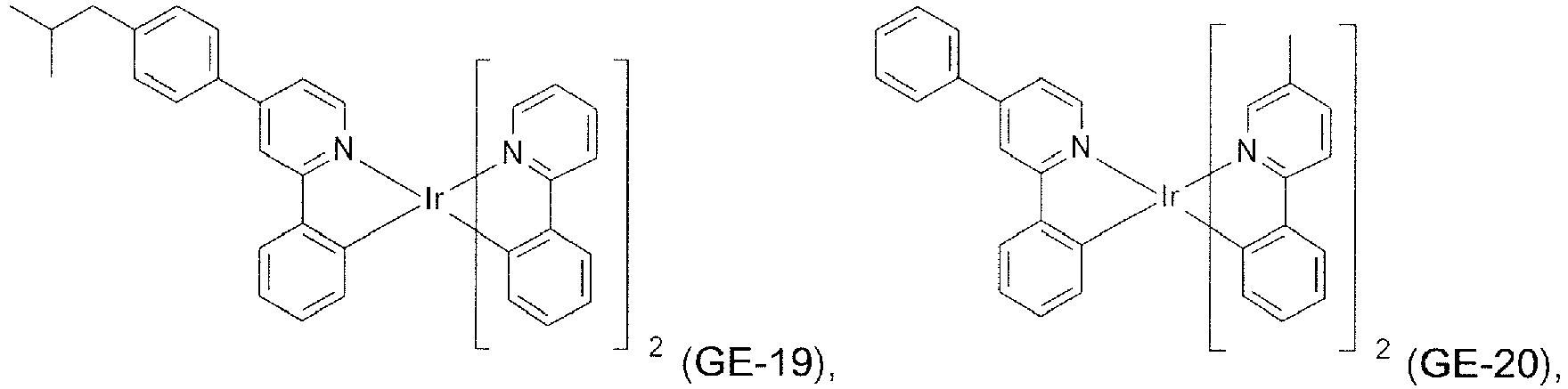
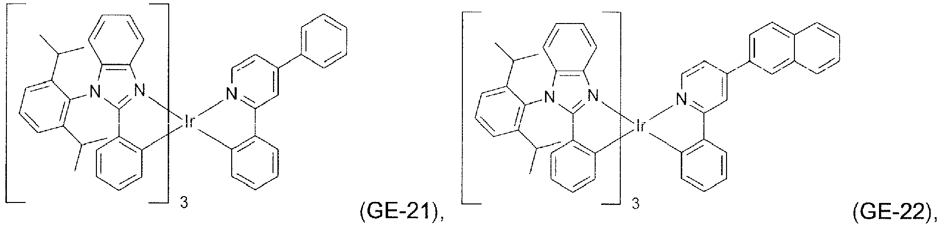
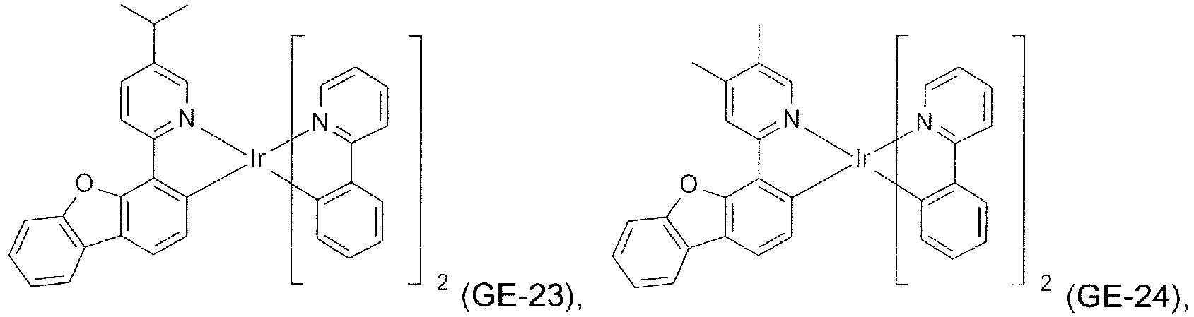
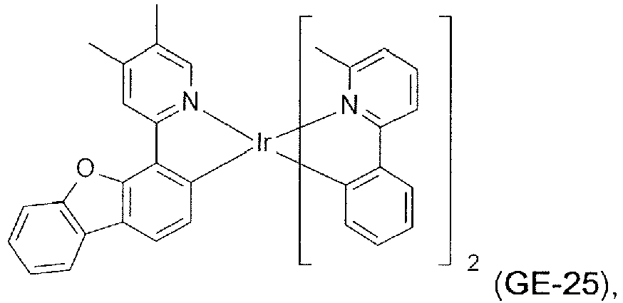
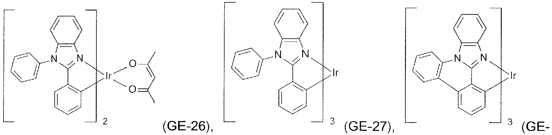
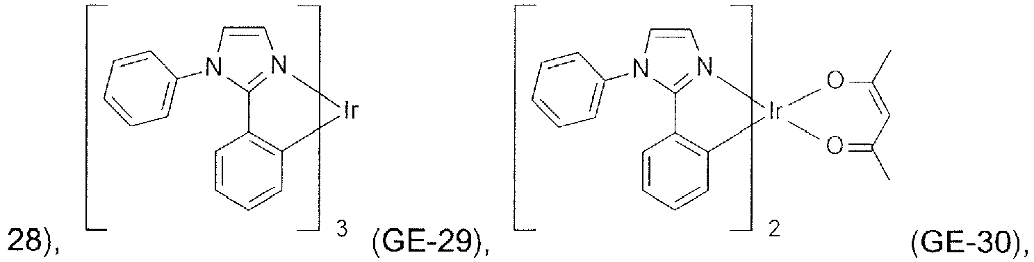

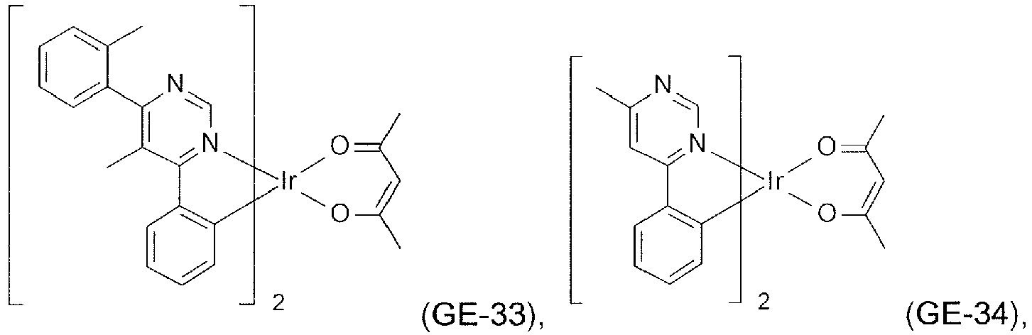
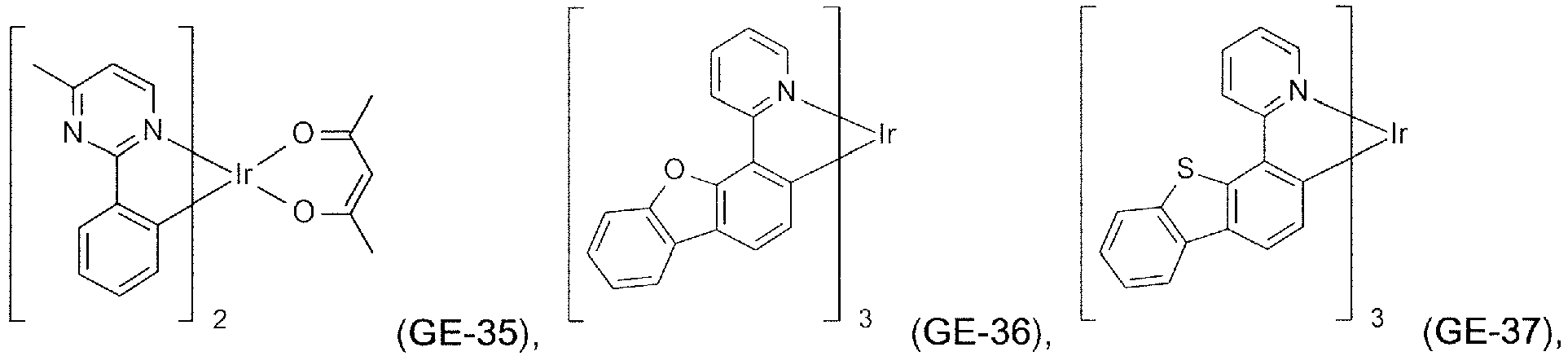
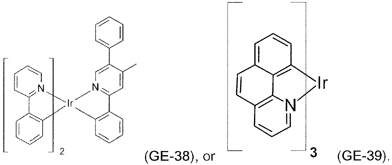
- The light-emitting layer may comprise further components in addition to the emitter material. For example, a fluroescent dye may be present in the light-emitting layer in order to alter the emission color of the emitter material. In addition - in a preferred embodiment - a matrix material can be used. This matrix material may be a polymer, for example poly(N-vinylcarbazole) or polysilane. The matrix material may, however, be a small molecule, for example 4,4'-N,N'dicarbazolebiphenyl (CDP=CBP) or tertiary aromatic amines, for example TCTA.
- In a preferred embodiment, the light-emitting layer is formed of at least one emitter material and of at least one of the matrix materials - in one embodiment at least one compound of the formula Ib. Suitable emitter materials and matrix materials are mentioned in the specification. In one embodiment, the light-emitting layer comprises at least one emitter material and at least to matrix materials, wherein one of the matrix materials is a first host material and the other is a second host material. The matrix materials mentioned in the specification are suitable as first and second host materials.
- In another preferred embodiment of the present invention, at least one compound of the formula Ib is used as host material. Examples of preferred compounds of formula Ib useful as host material are shown above.
- In a more preferred embodiment, the light-emitting layer is formed from 2 to 40% by weight, preferably 5 to 35% by weight, of at least one of the aforementioned emitter materials and 60 to 98% by weight, preferably 75 to 95% by weight, of at least one of the matrix materials mentioned in the specification - in one embodiment at least one compound of the formula Ib - where the sum total of the emitter material and of the matrix material adds up to 100% by weight.
- In a particularly preferred embodiment, the light-emitting layer comprises a compound of formula Ib and two carbene complexes, preferably BE-1 and HTM-1, or HTM-2. In said embodiment, the light-emitting layer is formed from 2 to 40% by weight, preferably 5 to 35% by weight, of BE-1 and 60 to 98% by weight, preferably 65 to 95% by weight, of a compound of the formula Ib and and HTM-1, or HTM-2, where the sum total of the carbene complexes and of the compound of formula Ib adds up to 100% by weight.
- Suitable metal complexes for use as matrix material in OLEDs, preferably together with the compounds of the formula Ib, are, for example, also carbene complexes as described in
WO 2005/019373 A2 ,WO 2006/056418 A2 ,WO 2005/113704 ,WO 2007/115970 ,WO 2007/115981 andWO 2008/000727 . - Further suitable host materials, which may be small molecules or (co)polymers of the small molecules mentioned, are specified in the following publications:
WO2007108459 (H-1 to H-37), preferably H-20 to H-22 and H-32 to H-37, most preferably H-20, H-32, H-36, H-37,WO2008035571 A1 (Host 1 to Host 6),JP2010135467 WO2009008100 compounds No.1 to No.67, preferably No.3, No.4, No.7 to No. 12, No.55, No.59, No. 63 to No.67, more preferably No. 4, No. 8 to No. 12, No. 55, No. 59, No.64, No.65, and No. 67,WO2009008099 compounds No. 1 to No. 110,WO2008140114 compounds 1-1 to 1-50,WO2008090912 compounds OC-7 to OC-36 and the polymers of Mo-42 to Mo-51,JP2008084913 WO2007077810 compounds 1 to 44, preferably 1, 2, 4-6, 8, 19-22, 26, 28-30, 32, 36, 39-44,WO201001830 WO2008029729 the (polymers of) compounds 1-1 to 1-36,WO20100443342 JP2009182298 JP2009170764 JP2009135183 WO2009063757 preferably the (co)polymers based on the monomers 1-1 to 1-26,WO2008146838 the compounds a-1 to a-43 and 1-1 to 1-46,JP2008207520 JP2008066569 WO2008029652 the (co)polymers based on the monomers 1-1 to 1-52,WO2007114244 the (co)polymers based on the monomers 1-1 to 1-18,JP2010040830 JP2009021336 WO2010090077 the compounds 1 to 55,WO2010079678 the compounds H1 to H42,WO2010067746 ,WO2010044342 the compounds HS-1 to HS-101 and Poly-1 to Poly-4,JP2010114180 US2009284138 the compounds 1 to 111 and H1 to H71,WO2008072596 the compounds 1 to 45,JP2010021336 WO2010004877 the compounds H-1 to H-60,JP2009267255 WO2009104488 the compounds 1-1 to 1-38,WO2009086028 ,US2009153034 ,US2009134784 ,WO2009084413 the compounds 2-1 to 2-56,JP2009114369 JP2009114370 WO2009060742 the compounds 2-1 to 2-56,WO2009060757 the compounds 1-1 to 1-76,WO2009060780 the compounds 1-1 to 1-70,WO2009060779 the compounds 1-1 to 1-42,WO2008156105 the compounds 1 to 54,JP2009059767 JP2008074939 JP2008021687 WO2007119816 the compounds 1 to 37,WO2010087222 the compounds H-1 to H-31,WO2010095564 the compounds HOST-1 to HOST-61,WO2007108362 ,WO2009003898 ,WO2009003919 ,WO2010040777 ,US2007224446 ,WO06128800 WO2012014621 ,WO2012105310 ,WO2012/130709 and European patent applicationsEP12175635.7 EP12185230.5 EP12191408.9 EP12191408.9 - The above-mentioned small molecules are more preferred than the above-mentioned (co)polymers of the small molecules.
- Further suitable host materials, are described in
WO2011137072 (for example,
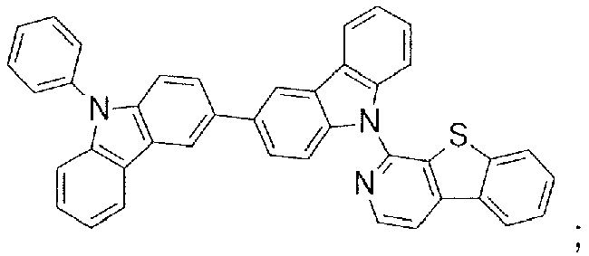

WO2012048266 (for example,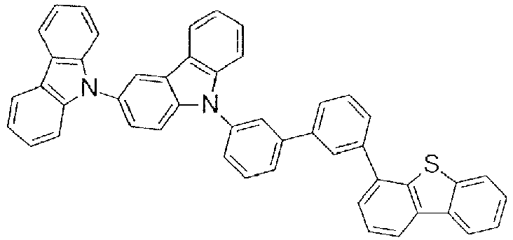
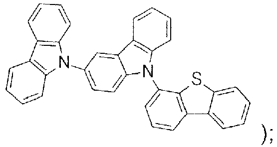
WO2012162325 (for example,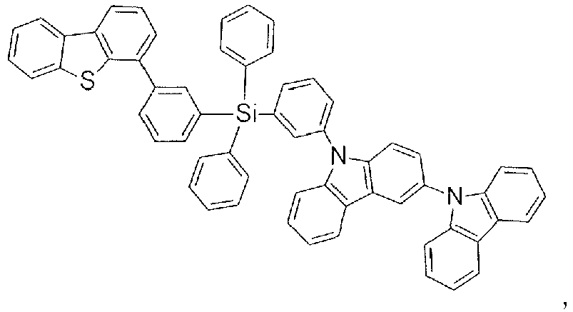


EP2551932 (for example,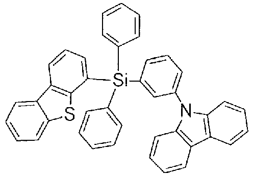
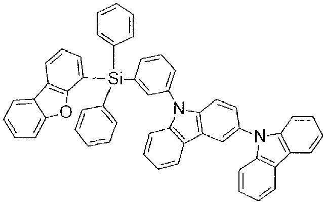
- In a particularly preferred embodiment, one or more compounds of the general formula (XV) specified hereinafter are used as host material.
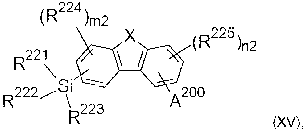
- X is NR, S, O or PR;
- R is aryl, heteroaryl, alkyl, cycloalkyl, or heterocycloalkyl;
- A200 is -NR206R207, -P(O)R208R209, -PR210R211, -S(O)2R212, -S(O)R213, -SR214, or -OR215;
- R221, R222 and R223 are independently of each other aryl, heteroaryl, alkyl, cycloalkyl, or heterocycloalkyl, wherein at least on of the groups R221, R222, or R223 is aryl, or heteroaryl;
- R224 and R225 are independently of each other alkyl, cycloalkyl, heterocycloalkyl, aryl, heteroaryl, a group A200, or a group having donor, or acceptor characteristics;
- n2 and m2 are independently of each other 0, 1, 2, or 3;
- R206 and R207 form together with the nitrogen atom a cyclic residue having 3 to 10 ring atoms, which can be unsubstituted, or which can be substituted with one, or more substituents selected from alkyl, cycloalkyl, heterocycloalkyl, aryl, heteroaryl and a group having donor, or acceptor characteristics; and/or which can be annulated with one, or more further cyclic residues having 3 to 10 ring atoms, wherein the annulated residues can be unsubstituted, or can be substituted with one, or more substituents selected from alkyl, cycloalkyl, heterocycloalkyl, aryl, heteroaryl and a group having donor, or acceptor characteristics; and
- R208, R209, R210, R211, R212, R213, R214 und R215 are independently of each other aryl, heteroaryl, alkyl, cycloalkyl, or heterocycloalkyl. Compounds of formula XV, such as, for example,
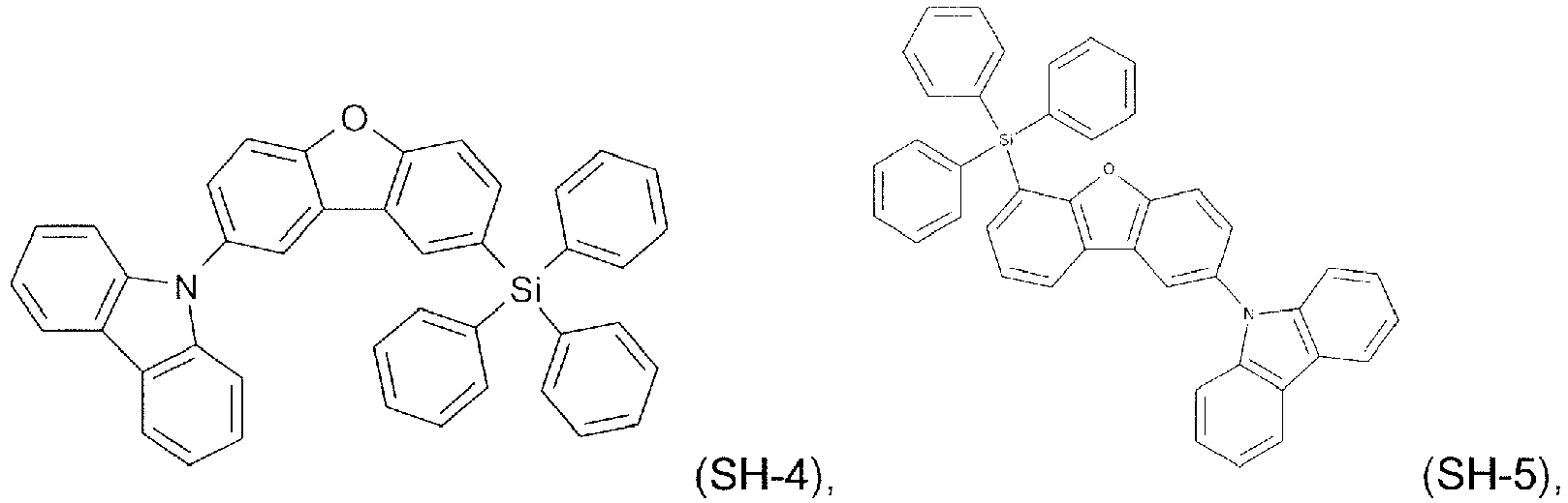
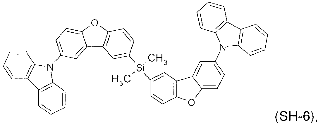
WO2010079051 (in particular pages on 19 to 26 and in tables on pages 27 to 34, pages 35 to 37 and pages 42 to 43). - Additional host materials on basis of dibenzofurane are, for example, described in
US2009066226 ,EP1885818B1 ,EP1970976 ,EP1998388 ,EP2034538 and European patent application no.14160197.1 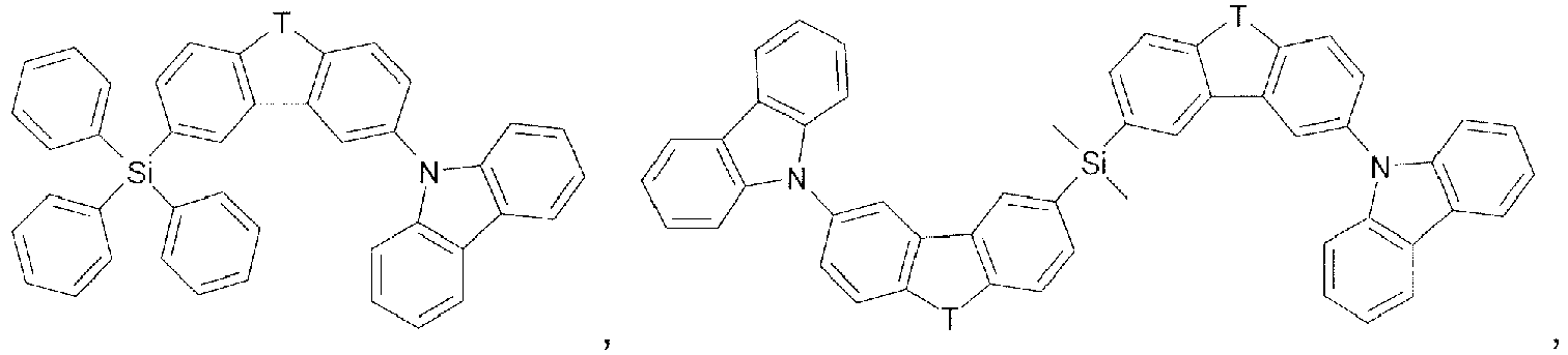


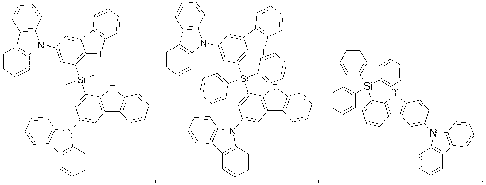


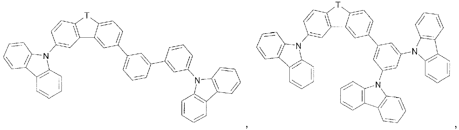
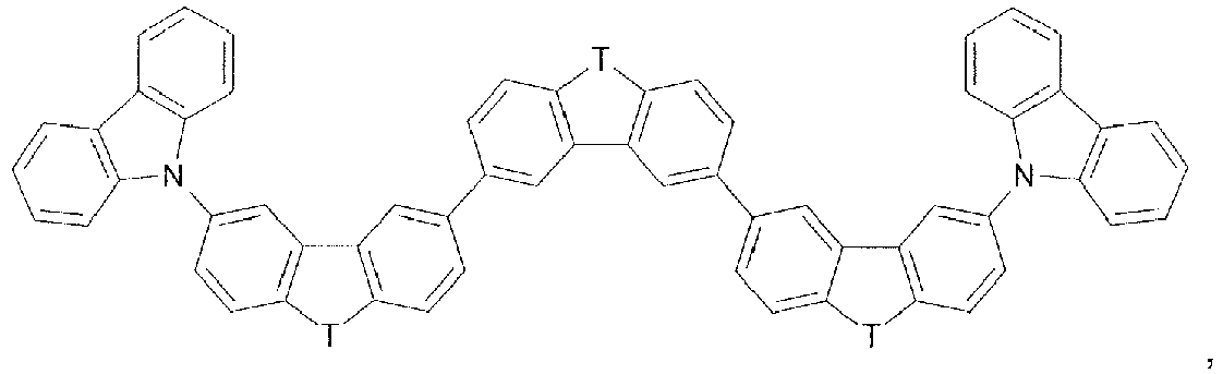
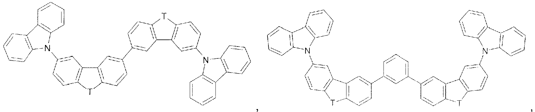
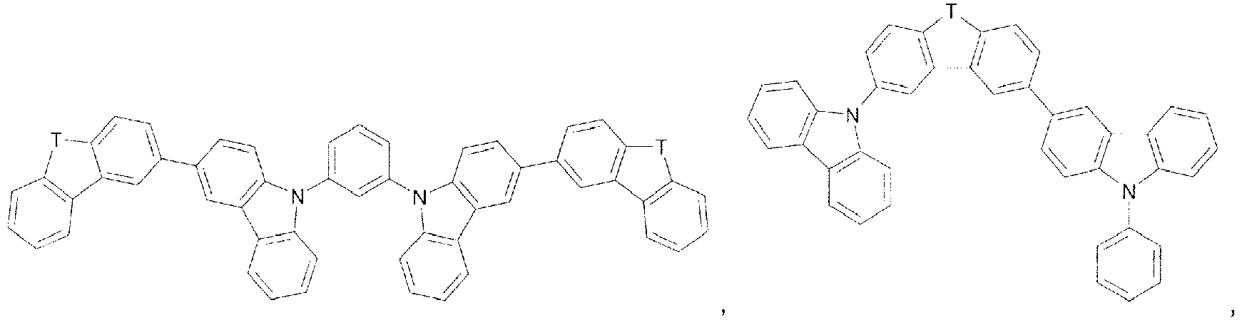
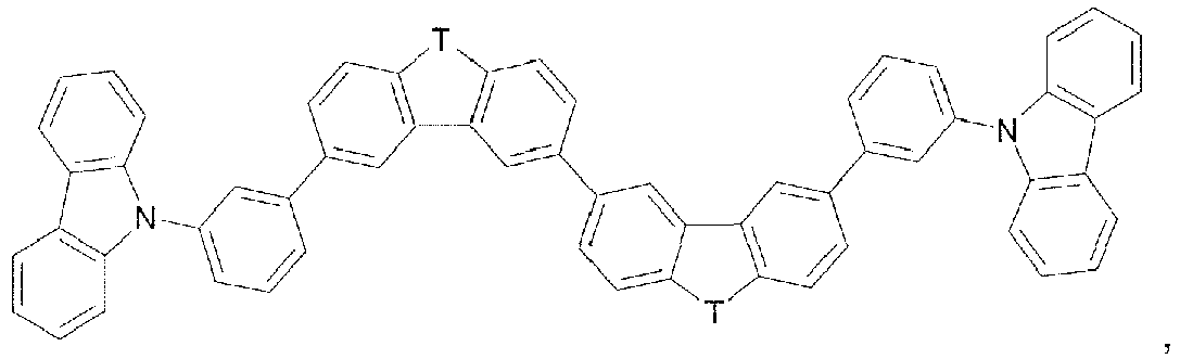

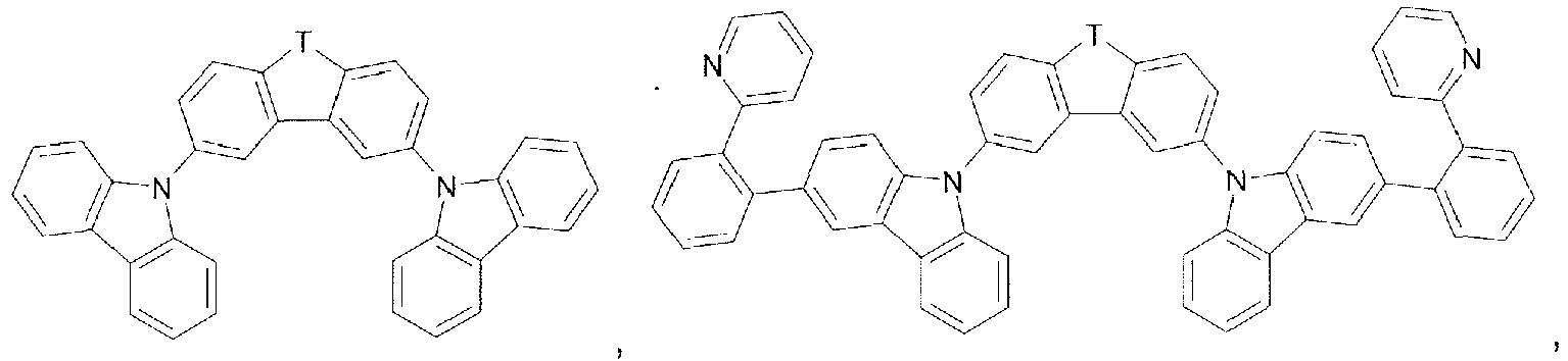
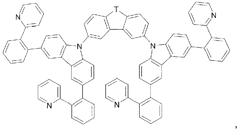
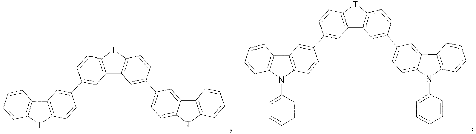
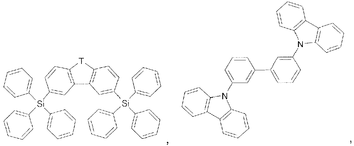
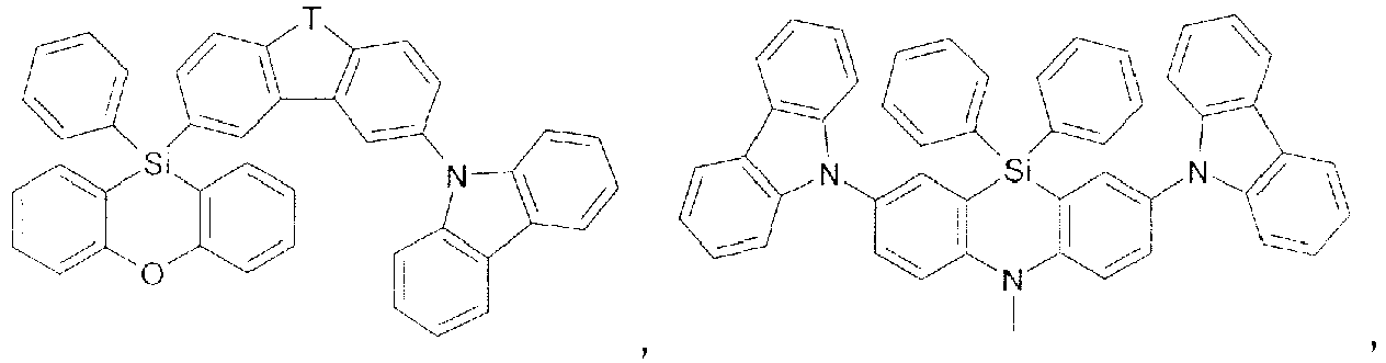
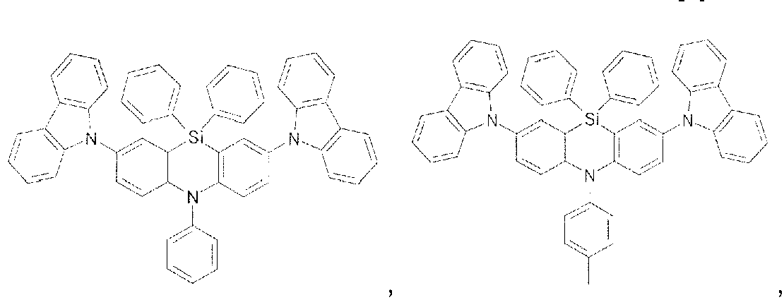
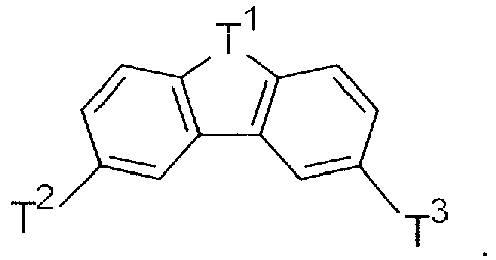
- In the above-mentioned compounds T is O, or S, preferably O. If T occurs more than one time in a molecule, all groups T have the same meaning. T1 is O, or S, preferably O. T1 and T2 are independently of each other
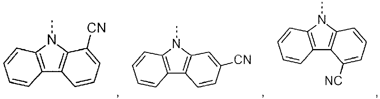
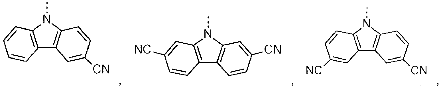

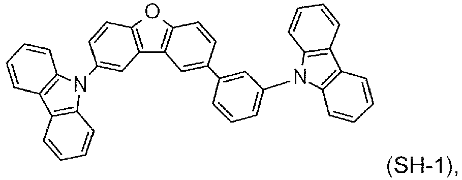
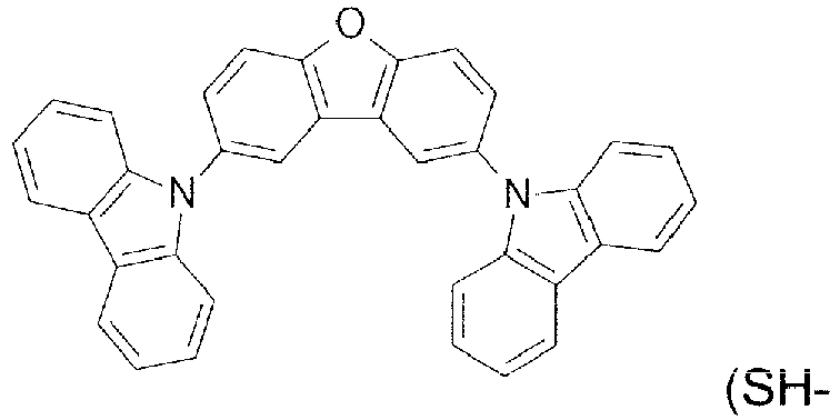
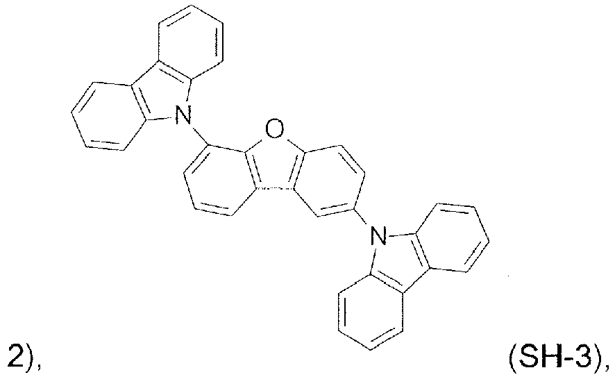
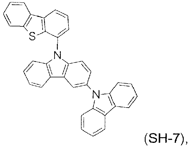
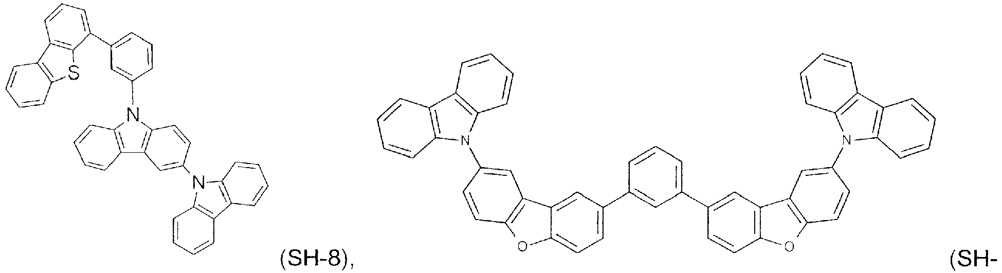
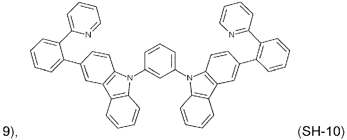
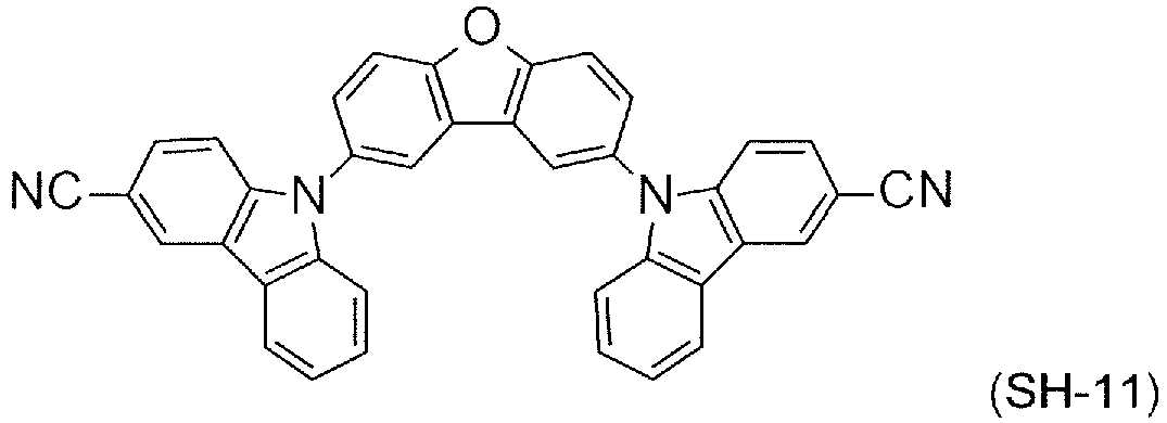
- In a further embodiment of the present invention, the compounds of formula Ib are employed as TADF material in the light-emitting layer of an OLED. The compounds of formula Ib are used as TADF emitter or as TADF host materials in combination with fluorescent emitters.
- Suitable host materials in combination with the compounds of formula Ib as emitter material as well as suitable fluorescent emitter material in combination with the compounds of formula Ib as TADF host material are known by a person skilled in the art.
- Blocking layers may be used to reduce the number of charge carriers (electrons or holes) and/or excitons that leave the emissive layer. The hole blocking layer may be disposed between the emitting layer (e) and electron transport layer (g), to block holes from leaving layer (e) in the direction of electron transport layer (g). Blocking layers may also be used to block excitons from diffusing out of the emissive layer.
- Additional hole blocker materials typically used in OLEDs are 2,6-bis(N-carbazolyl)pyridine (mCPy), 2,9-dimethyl-4,7-diphenyl-1,10-phenanthroline (bathocuproin, (BCP)), bis(2-methyl-8-quinolinato)-4-phenylphenylato)aluminum(III) (BAlq), phenothiazine S,S-dioxide derivates and 1,3,5-tris(N-phenyl-2-benzylimidazolyl)benzene) (TPBI), TPBI also being suitable as electron-transport material. Further suitable hole blockers and/or electron conductor materials are 2,2',2"-(1,3,5-benzenetriyl)tris(1-phenyl-1-H-benzimidazole), 2-(4-biphenylyl)-5-(4-tert-butylphenyl)-1,3,4-oxadiazole, 8-hydroxyquinolinolatolithium, 4-(naphthalen-1-yl)-3,5-diphenyl-4H-1,2,4-triazole, 1,3-bis[2-(2,2'-bipyridin-6-yl)-1,3,4-oxadiazo-5-yl]benzene, 4,7-diphenyl-1,10-phenanthroline, 3-(4-biphenylyl)-4-phenyl-5-tert-butylphenyl-1,2,4-triazole, 6,6'-bis[5-(biphenyl-4-yl)-1,3,4-oxadiazo-2-yl]-2,2'-bipyridyl, 2-phenyl-9,10-di(naphthalene-2-yl)anthracene, 2,7-bis[2-(2,2'-bipyridin-6-yl)-1,3,4-oxadiazo-5-yl]-9,9-dimethylfluorene, 1,3-bis[2-(4-tert-butylphenyl)-1,3,4-oxadiazo-5-yl]benzene, 2-(naphthalene-2-yl)-4,7-diphenyl-1,10-phenanthroline, tris(2,4,6-trimethyl-3-(pyridin-3-yl)phenyl)borane, 2,9-bis(naphthalene-2-yl)-4,7-diphenyl-1,10-phenanthroline, 1-methyl-2-(4-(naphthalene-2-yl)phenyl)-1H-imidazo[4,5-f][1,10]-phenanthroline. In a further embodiment, it is possible to use compounds which comprise aromatic or heteroaromatic rings joined via groups comprising carbonyl groups, as disclosed in
WO2006/100298 , disilyl compounds selected from the group consisting of disilylcarbazoles, disilylbenzofurans, disilylbenzothiophenes, disilylbenzophospholes, disilylbenzothiophene S-oxides and disilylbenzothiophene S,S-dioxides, as specified, for example, in PCT applicationsWO2009/003919 andWO2009003898 and disilyl compounds as disclosed inWO2008/034758 , as a blocking layer for holes/excitons (f). - In another preferred embodiment compounds (SH-1), (SH-2), (SH-3), SH-4, SH-5, SH-6, (SH-7), (SH-8), (SH-9), (SH-10) and (SH-11) may be used as hole/exciton blocking materials.
- Electron transport layer may include a material capable of transporting electrons. Electron transport layer may be intrinsic (undoped), or doped. Doping may be used to enhance conductivity. Suitable electron-transporting materials for layer (g) of the inventive OLEDs comprise metals chelated with oxinoid compounds, such as tris(8-hydroxyquinolato)aluminum (Alq3), compounds based on phenanthroline such as 2,9-dimethyl-4,7-diphenyl-1,10-phenanthroline (DDPA = BCP), 4,7-diphenyl-1,10-phenanthroline (Bphen), 2,4,7,9-tetraphenyl-1,10-phenanthroline, 4,7-diphenyl-1,10-phenanthroline (DPA) or phenanthroline derivatives disclosed in
EP1786050 , inEP1970371 , or inEP1097981 , and azole compounds such as 2-(4-biphenylyl)-5-(4-t-butylphenyl)-1,3,4-oxadiazole (PBD) and 3-(4-biphenylyl)-4phenyl-5-(4-t-butylphenyl)-1,2,4-triazole (TAZ). - It is likewise possible to use mixtures of at least two materials in the electron-transporting layer, in which case at least one material is electron-conducting. Preferably, in such mixed electron-transport layers, at least one phenanthroline compound is used, preferably BCP, or at least one pyridine compound according to the formula (XVI) below, preferably a compound of the formula (XVIa) below. More preferably, in mixed electron-transport layers, in addition to at least one phenanthroline compound, alkaline earth metal or alkali metal hydroxyquinolate complexes, for example Liq, are used. Suitable alkaline earth metal or alkali metal hydroxyquinolate complexes are specified below (formula XVII). Reference is made to
WO2011/157779 . - The electron-transport layer may also be electronically doped in order to improve the transport properties of the materials used, in order firstly to make the layer thicknesses more generous (avoidance of pinholes/short circuits) and in order secondly to minimize the operating voltage of the device. Electronic doping is known to those skilled in the art and is disclosed, for example, in W. Gao, A. Kahn, J. Appl. Phys., Vol. 94, No. 1, 1 July 2003 (p-doped organic layers); A. G. Werner, F. Li, K. Harada, M. Pfeiffer, T. Fritz, K. Leo, Appl. Phys. Lett., Vol. 82, No. 25, 23 June 2003 and Pfeiffer et al., Organic Electronics 2003, 4, 89 - 103 and K. Walzer, B. Maennig, M. Pfeiffer, K. Leo, Chem. Soc. Rev. 2007, 107, 1233. For example, it is possible to use mixtures which lead to electrical n-doping of the electron-transport layer. n-Doping is achieved by the addition of reducing materials. These mixtures may, for example, be mixtures of the abovementioned electron transport materials with alkali/alkaline earth metals or alkali/alkaline earth metal salts, for example Li, Cs, Ca, Sr, Cs2CO3, with alkali metal complexes, for example 8-hydroxyquinolatolithium (Liq), and with Y, Ce, Sm, Gd, Tb, Er, Tm, Yb, Li3N, Rb2CO3, dipotassium phthalate, W(hpp)4 from
EP1786050 , or with compounds described inEP1837926B1 ,EP1837927 ,EP2246862 andWO2010132236 . - In a preferred embodiment, the electron-transport layer comprises at least one compound of the general formula (XVII)
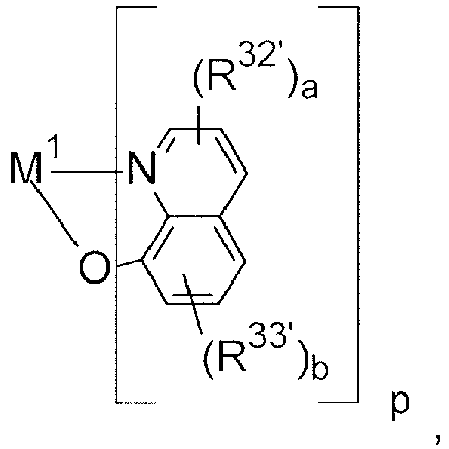
- R32' and R33' are each independently F, C1-C8-alkyl, or C6-C14-aryl, which is optionally substituted by one or more C1-C8-alkyl groups, or
- two R32' and/or R33' substituents together form a fused benzene ring which is optionally substituted by one or more C1-C8-alkyl groups;
- a and b are each independently 0, or 1, 2 or 3,
- M1 is an alkaline metal atom or alkaline earth metal atom,
- p is 1 when M1 is an alkali metal atom, p is 2 when M1 is an earth alkali metal atom.
- A very particularly preferred compound of the formula (XVII) is

- In a further preferred embodiment, the electron-transport layer comprises at least one compound of the formula (XVI),
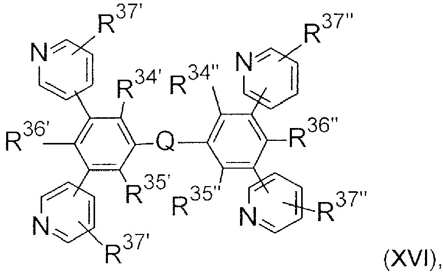
- R34", R35", R36", R37", R34', R35', R36' and R37' are each independently H, C1-C18-alkyl, C1-C18-alkyl which is substituted by E' and/or interrupted by D', C6-C24-aryl, C6-C24-aryl which is substituted by G', C2-C20-heteroaryl or C2-C20-heteroaryl which is substituted by G',
- Q is an arylene or heteroarylene group, each of which is optionally substituted by G';
- D' is -CO-; -COO-; -S-; -SO-; -SO2-; -O-; -NR40'-; -SiR45'R46'-; -POR47'-; -CR38'=CR39'-; or -C≡C-; E' is -OR44'; -SR44'; -NR40'R41'; -COR43'; -COOR42'; -CONR40'R41'; -CN; or F;
- G' is E', C1-C18-alkyl, C1-C18-alkyl which is interrupted by D', C1-C18-perfluoroalkyl, C1-C18-alkoxy, or C1-C18-alkoxy which is substituted by E' and/or interrupted by D', in which R38' and R39' are each independently H, C6-C18-aryl; C6-C18-aryl which is substituted by C1-C18-alkyl or C1-C18-alkoxy; C1-C18-alkyl; or C1-C18-alkyl which is interrupted by -O-;
- R40' and R41' are each independently C6-C18-aryl; C6-C18-aryl which is substituted by C1-C18-alkyl or C1-C18-alkoxy; C1-C18-alkyl; or C1-C18-alkyl which is interrupted by -O-; or R40' and R41' together form a 6-membered ring;
- R42' and R43' are each independently C6-C18-aryl; C6-C18-aryl which is substituted by C1-C18-alkyl or C1-C18-alkoxy; C1-C18-alkyl; or C1-C18-alkyl which is interrupted by -O-,
- R44' is C6-C18-aryl; C6-C18-aryl which is substituted by C1-C18-alkyl or C1-C18-alkoxy; C1-C18-alkyl; or C1-C18-alkyl which is interrupted by -O-,
- R45' and R46' are each independently C1-C18-alkyl, C6-C18-aryl or C6-C18-aryl which is substituted by C1-C18-alkyl,
- R47' is C1-C18-alkyl, C6-C18-aryl or C6-C18-aryl which is substituted by C1-C18-alkyl.
- Preferred compounds of the formula (XVI) are compounds of the formula (XVIa)
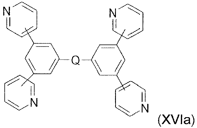
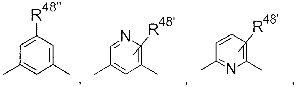
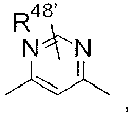
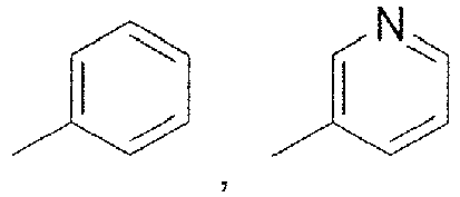

- Particular preference is given to a compound of the formula
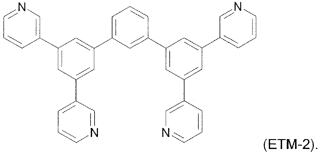
- In a further, very particularly preferred embodiment, the electron-transport layer comprises a compound Liq and a compound ETM-2.
- In a preferred embodiment, the electron-transport layer comprises at least one compound of the formula (XVII) in an amount of 99 to 1% by weight, preferably 75 to 25% by weight, more preferably about 50% by weight, and at least one compound of the formula (XVI) in an amount of 1 to 99% by weight, preferably 25 to 75% by weight, more preferably about 50% by weight, where the amount of the compounds of the formulae (XVII) and the amount of the compounds of the formulae (XVI) adds up to a total of 100% by weight.
- The preparation of the compounds of the formula (XVI) is described in J. Kido et al., Chem. Commun. (2008) 5821-5823, J. Kido et al., Chem. Mater. 20 (2008) 5951-5953 and
JP2008/127326 - It is likewise possible to use mixtures of alkali metal hydroxyquinolate complexes, preferably Liq, and dibenzofuran compounds in the electron-transport layer. Reference is made to
WO2011/157790 . Dibenzofuran compounds A-1 to A-36 and B-1 to B-22 described inWO2011/157790 are preferred, wherein dibenzofuran compound
- In a preferred embodiment, the electron-transport layer comprises Liq in an amount of 99 to 1% by weight, preferably 75 to 25% by weight, more preferably about 50% by weight, and at least one dibenzofuran compound in an amount of 1 to 99% by weight, preferably 25 to 75% by weight, more preferably about 50% by weight, where the amount of Liq and the amount of the dibenzofuran compound(s), especially ETM-1, adds up to a total of 100% by weight.
- In a preferred embodiment, the electron-transport layer comprises at least one phenanthroline derivative and/or pyridine derivative.
- In a further preferred embodiment, the electron-transport layer comprises at least one phenanthroline derivative and/or pyridine derivative and at least one alkali metal hydroxyquinolate complex.
- In a further preferred embodiment, the electron-transport layer comprises at least one of the dibenzofuran compounds A-1 to A-36 and B-1 to B-22 described in
WO2011/157790 , especially ETM-1. - In a further preferred embodiment, the electron-transport layer comprises a compound described in
WO2012/111462 ,WO2012/147397 ,WO2012014621 , such as, for example, a compound of formula
US2012/0261654 , such as, for example, a compound of formula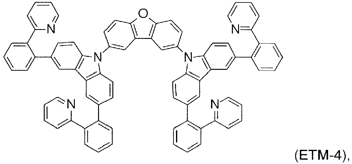
WO2012/115034 , such as for example, such as, for example, a compound of formula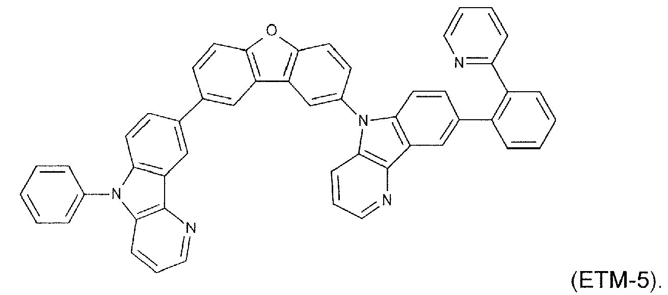
- The electron injection layer may be any layer that improves the injection of electrons into an adjacent organic layer. Lithium-comprising organometallic compounds such as 8-hydroxyquinolatolithium (Liq), CsF, NaF, KF, Cs2CO3 or LiF may be applied between the electron transport layer (g) and the cathode (i) as an electron injection layer (h) in order to reduce the operating voltage.
- The cathode (i) is an electrode which serves to introduce electrons or negative charge carriers. The cathode may be any metal or nonmetal which has a lower work function than the anode. Suitable materials for the cathode are selected from the group consisting of alkali metals of group 1, for example Li, Cs, alkaline earth metals of group 2, metals of group 12 of the Periodic Table of the Elements, comprising the rare earth metals and the lanthanides and actinides. In addition, metals such as aluminum, indium, calcium, barium, samarium and magnesium, and combinations thereof, may be used.
- In general, the different layers, if present, have the following thicknesses:
- anode (a): 500 to 5000 Å (ångström), preferably 1000 to 2000 Å;
- hole injection layer (b): 50 to 1000 Å, preferably 200 to 800 Å,
- hole-transport layer (c): 50 to 1000 Å, preferably 100 to 800 Å,
- exciton blocking layer (d): 10 to 500 Å, preferably 50 to 100 Å,
- light-emitting layer (e): 10 to 1000 A, preferably 50 to 600 Å,
- hole/ exciton blocking layer (f): 10 to 500 Å, preferably 50 to 100 Å,
- electron-transport layer (g): 50 to 1000 Å, preferably 200 to 800 Å,
- electron injection layer (h): 10 to 500 Å, preferably 20 to 100 Å,
- cathode (i): 200 to 10 000 Å, preferably 300 to 5000 Å.
- The person skilled in the art is aware (for example on the basis of electrochemical studies) of how suitable materials have to be selected. Suitable materials for the individual layers are known to those skilled in the art and are disclosed, for example, in
WO 00/70655 - In addition, it is possible that some of the layers used in the inventive OLED have been surface-treated in order to increase the efficiency of charge carrier transport. The selection of the materials for each of the layers mentioned is preferably determined by obtaining an OLED with a high efficiency and lifetime.
- The inventive OLED can be produced by methods known to those skilled in the art. In general, the inventive OLED is produced by successive vapor deposition of the individual layers onto a suitable substrate. Suitable substrates are, for example, glass, inorganic semiconductors or polymer films. For vapor deposition, it is possible to use customary techniques, such as thermal evaporation, chemical vapor deposition (CVD), physical vapor deposition (PVD) and others. In an alternative process, the organic layers of the OLED can be applied from solutions or dispersions in suitable solvents, employing coating techniques known to those skilled in the art.
- Use of the compounds of the formula Ib in at least one layer of the OLED, preferably in the light-emitting layer (preferably as a matrix material), charge transport layer and/or in the charge/exciton blocking layer makes it possible to obtain OLEDs with high efficiency and with low use and operating voltage. Frequently, the OLEDs obtained by the use of the compounds of the formula Ib additionally have high lifetimes. The efficiency of the OLEDs can additionally be improved by optimizing the other layers of the OLEDs. For example, high-efficiency cathodes such as Ca or Ba, if appropriate in combination with an intermediate layer of LiF, can be used. Moreover, additional layers may be present in the OLEDs in order to adjust the energy level of the different layers and to facilitate electroluminescence.
- The OLEDs may further comprise at least one second light-emitting layer. The overall emission of the OLEDs may be composed of the emission of the at least two light-emitting layers and may also comprise white light.
- The OLEDs can be used in all apparatus in which electroluminescence is useful. Suitable devices are preferably selected from stationary and mobile visual display units and illumination units. Stationary visual display units are, for example, visual display units of computers, televisions, visual display units in printers, kitchen appliances and advertising panels, illuminations and information panels. Mobile visual display units are, for example, visual display units in cellphones, tablet PCs, laptops, digital cameras, MP3 players, vehicles and destination displays on buses and trains. Further devices in which the inventive OLEDs can be used are, for example, keyboards; items of clothing; furniture; wallpaper. In addition, the present invention relates to a device selected from the group consisting of stationary visual display units such as visual display units of computers, televisions, visual display units in printers, kitchen appliances and advertising panels, illuminations, information panels, and mobile visual display units such as visual display units in cellphones, tablet PCs, laptops, digital cameras, MP3 players, vehicles and destination displays on buses and trains; illumination units; keyboards; items of clothing; furniture; wallpaper, comprising at least one inventive organic light-emitting diode or at least one inventive light-emitting layer.
- The following examples are included for illustrative purposes only and do not limit the scope of the claims. Comparative examples are for reference only. Unless otherwise stated, all parts and percentages are by weight.
-

- 2.92 g (20.0 mmol) of 1,3-dicyano-5-fluoro-benzene, 4.14 g (20.0 mmol) of 6H-benzimidazolo[1,2-a]benzimidazole and 4.25 g (20.0 mmol) of tripotassium phosphate in 50 ml of DMF are stirred for 2 h at 120 °C. The reaction mixture is cooled at room temperature and added water, then the precipitate is filterted off. Gradient column chromatography on silica gel with dichloromethane/ethyl acetate (dichloromethane100%, 9/1, 4/1) gives the product. Yield 6.13 g (92 %).
1H NMR (400 MHz, CDCl3): δ 8.61 (d, 2H); 7.96 (t, 1H); 7.89 (td, 2H); 7.83 (dd, 1H); 7.66 (dd, 1H); 7.52 (td, 1H); 7.49 - 7.43 (m, 2H); 7.40 (td, 1H). -

- 1.63 g (10.0 mmol) of 2-chloro-1,3-dicyano-benzene, 2.07 g (10.0 mmol) of 6H-benzimidazolo[1,2-a]benzimidazole and 2.12 g (10.0 mmol) of tripotassium phosphate in 50 ml of DMF are stirred for 24 h at 150 °C. The reaction mixture is cooled at room temperature and added water, then the precipitate is filterted off. Gradient column chromatography on silica gel with dichloromethane/ethyl acetate (dichloromethane100%, 9/1, 4/1) gives the product. Yield 2.80 g (84 %).
1H NMR (400 MHz, CDCl3): δ 8.19 (d, 2H); 7.95 - 7.87 (m, 2H); 7.86 (t, 1H); 7.79 (dd, 1H); 7.49 (td, 1H); 7.46 - 7.35 (m, 3H); 7.15 (dt, 1H). -
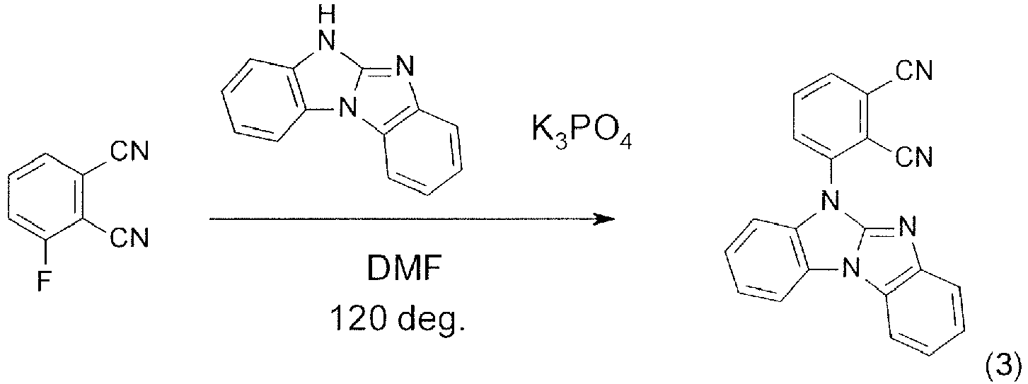
- 1.46 g (10.0 mmol) of 1,2-dicyano-3-fluoro-benzene, 2.07 g (10.0 mmol) of 6H-benzimidazolo[1,2-a]benzimidazole and 2.12 g (10.0 mmol) of tripotassium phosphate in 50 ml of DMF are stirred for 24 h at 120 °C. The reaction mixture is cooled at room temperature and added water, then the precipitate is filterted off. Gradient column chromatography on silica gel with dichloromethane/ethyl acetate (dichloromethane100%, 9/1, 4/1) gives the product. Yield 3.10 g (93 %).
1H NMR (400 MHz, CDCl3): δ 8.20 (dd, 1H); 8.05 - 7.96 (m, 2H); 7.90 (dd, 2H); 7.79 (dd, 1H); 7.49 (td, 1H); 7.46 - 7.36 (m, 3H); 7.32 - 7.26 (m, 1H). -

- 0.98 g (6.71 mmol) of 1,3-dicyano-5-fluoro-benzene, 2.50 g (6.71 mmol) of 6-(3-carbazolyl)-benzimidazolo[1,2-a]benzimidazole and 1.42 g (6.71 mmol) of tripotassium phosphate in 20 ml of DMF are stirred for 24 h at 120 °C. The reaction mixture is cooled at room temperature and added water, then the precipitate is filterted off. Gradient column chromatography on silica gel with dichloromethane/ethyl acetate (dichloromethane100%, 9/1, 4/1) gives the product. Yield 2.94 g (88 %).
1H NMR (400 MHz, CDCl3): δ 8.56 (dd, 1H); 8.24 (d, 2H); 8.23-8.19 (m, 1H); 8.07 (t, 1H); 7.94 - 7.89 (m, 3H); 7.81 (dt, 1H); 7.62 (dd, 1H); 7.60 - 7.53 (m, 2H); 7.48 - 7.32 (m, 6H). -
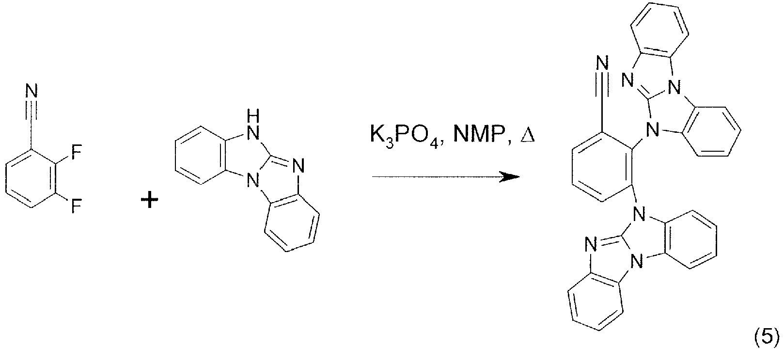
- 5.00 g (36.0 mmol) 2,3-difluorobenzonitrile, 14.9 g (72.0 mmol) 6H-benzimidazolo[1,2-a]benzimidazole and 30.5 (144 mmol) potassium phosphate tribasic in 120 ml NMP (N-Methyl-2-pyrrolidon) are stirred at 185 °C under nitrogen for 6 h.
- The reaction mixture is filtered hot and the organic phase is poured on water. The product is filtered of. Column chromatography on silica gel with chloroform gives 6.25 g 33.9 % of the product.
1H NMR (300 MHz, DMSO-D6): rotamers: δ 8.43-8.57 (m, 2H), 7.58-8.20 (m, 6H), 6.86-7.42 (m, 9H), 6.63-7.78 (m, 1H), 6.48-6.54 (m, 1H). -
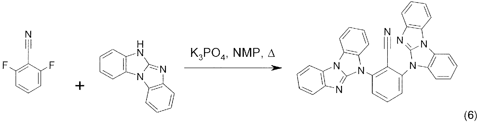
- 5.00 g (36.0 mmol) 2,6-difluorobenzonitrile, 14.9 g (72.0 mmol) 6H-benzimidazolo[1,2-a]benzimidazole and 30.5 g (144 mmol) potassium phosphate tribasic in 150 ml NMP (N-Methyl-2-pyrrolidon) are stirred at 170 °C under nitrogen for 6 h. The reaction mixture is filtered hot and the precipitated product was filtered of. The product is decocted in DMSO. Yield 3 g 16.3 % of the product.
1H NMR (400 MHz, TFA-d1): δ 8.48-8.78 (m, 3H), 8.24-8.32 (m, 4H), 7.67-7.93 (m, 12H). -
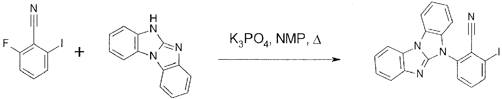
- A.) 10.6 g (41.6 mmol) 2-bromo-6-fluoro-benzonitrile, 8.63 g (41.6 mmol) 6H-benzimidazolo[1,2-a]benzimidazole and 30.9 (146 mmol) potassium phosphate tribasic in 70 ml NMP (N-Methyl-2-pyrrolidon) are stirred at 115 °C under nitrogen for 2 h. The reaction mixture is filtered hot and the or organic phase is poured on water. The product is filtered of. Yield 17 g (94 %).
1H NMR (300 MHz, DMSO-D6): δ 8.22-8.34 (m, 3H), 8.02-8.05 (m, 1H), 7.69-7.79 (m, 1H), 7.60-7.65 (m, 1H), 7.30-7.50 (m, 5H)
- B.) 6.52 g (15.0 mmol) 2-(benzimidazolo[1,2-a]benzimidazol-5-yl)-6-iodo-benzonitrile, 2.51 g (15.0 mmol) carbazole, 12.8 g (60.0 mmol) potassium phosphate tribasic, 0.430 g (2.00 mmol) cupper(I) iodide and 4.00 g (35.0 mmol) DACH ((±)-trans-1,2-diaminocyclohexane) in 75 ml mml dioxane are stirred at 95 °C under nitrogen for 24 h.
- The reaction mixture is filtered hot and the solids are washed with dioxane. The solvent is removed in vacuum. Column chromatography on silica gel with chloroform gives 1.53 g 22 % of the product.
1H NMR (300 MHz, DMSO-D6): δ 8.25-8.34 (m, 6H), 8.08-8.11 (m, 1H), 7.31-7.70 (m, 12H) MS (ESI(pos), m/z): 474 (M+1). -
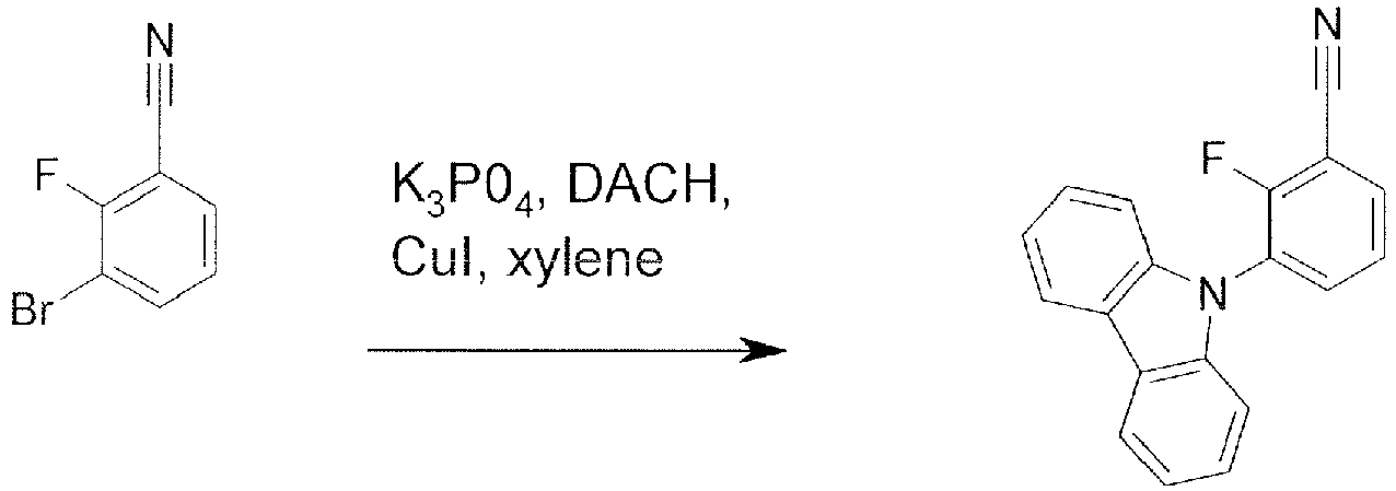
- A.)15.0 g 3-bromo-2-fluoro-benzonitrile (75.0 mmol), 12.9 g (77.0 mmol) carbazole, 47.8 g (225 mmol) potassium phosphate tribasic, 1.43 g (7.00 mmol) cupper(I) iodide and 1.71 g (15.0 mmol) DACH ((±)-trans-1,2-diaminocyclohexane) in 150 ml xylene are stirred at 115 °C under nitrogen for 20 h.
The reaction mixture is filtered hot and the solids are washed with Xylene. The solvent is removed in vacuum. Column chromatography on silica gel with chloroform/heptane 1 to 1 gives 5.7 g 27 % of the product.
1H NMR (300 MHz, DMSO-D6): δ 8.29 (s, 1H), 8.27 (s, 1H), 8.13-8.20 (m,1H), 7.67-7.73 (m, 1H), 7.44-7.50 (m 2H), 7.29-7.37 (m 4H)
- B.)3.50 g (12.2 mmol) 3-carbazol-9-yl-2-fluoro-benzonitrile, 2.58 g (12.5 mmol) 6H-benzimidazolo[1,2-a]benzimidazole and 10.3 g (50 mmol) potassium phosphate tribasic in 35 ml NMP (N-Methyl-2-pyrrolidon) are stirred at 170 °C under nitrogen for 18 h.
- The reaction mixture is filtered hot and the precipitated product was filtered of. Column chromatography on silica gel with dichloromethane gives 1.70 g 29 % of the product.
1H NMR (300 MHz, DMSO-D6): δ 8.46 (dd, 1H), 8.29 (dd. 1H), 8.13 (t, 1H), 7.96-8.00 (m, 2H), 7.85 (d, 1H), 7.80 (d, 1H), 7.67 (d, 1H), 7.58 (d, 1H), 7.41-7.46 (m, 1H), 7.31-7.37 (m, 1H) 7.22-7.27 (m, 2H), 7.00-7.707 (m, 2H), 6.87-6.93 (m, 2H), 6.66-6.73 (m, 2H).
MS (ESI(pos), m/z): 474 (M+1). -

- A.) 10.6 g (41.6 mmol) 2-fluoro-6-iodo-benzonitrile, 8.63 g (41.6 mmol) 6H-benzimidazolo[1,2-a]benzimidazole and 30.9 (146 mmol) potassium phosphate tribasic in 70 ml NMP (N-Methyl-2-pyrrolidon) are stirred at 115 °C under nitrogen for 2 h.
The reaction mixture is filtered hot and the organic phase is poured on water. The product is filtered of. Yield 17 g (94 %)
1H NMR (300 MHz, DMSO-D6): δ 8.22-8.34 (m, 3H), 8.02-8.05 (m, 1H), 7.69-7.79 (m, 1H), 7.60-7.65 (m, 1H), 7.30-7.50 (m, 5H)
- B.) 4.20 g (9.67 mmol) 2-(benzimidazolo[1,2-a]benzimidazol-5-yl)-6-iodo-benzonitrile, 4.44 g (9,67 mmol) 9-[8-(4,4,5,5-tetramethyl-1,3,2-dioxaborolan-2-yl)dibenzofuran-2-yl]carbazole, 8.21 g (39.0 mmol) potassium phosphate tribasic in 30 ml dioxane, 60 ml toluene and 24 ml water are degased with argon. 0.2 g (0.9 mmol) palladium(II)acetate is added and the reaction mixture is degased with argon. 0.93 g (2.2 mmol) SPhos (2-Dicyclohexylphosphino-2',6'-dimethoxybiphenyl) is added and the reaction mixture is degased with argon. The reaction mixture is refluxed under argon for 18 h.
- The organic layer is washed with a 1 % solution of NaCN in water and then the organic phase is washed with water. The organic phase is dried with Magnesium sulfate and the solvent is removed in vacuum.
- Column chromatography on silica gel with dichloromethane gives 1.450 g 23 % of the product.
1H NMR (300 MHz, DMSO-D6): δ 8.58-8.71 (m, 2H), 7.78-8.31 (m, 11H), 7.59-7.65 (m, 1H), 7.25-7.50 (m, 11H)
MS (APCI(pos), m/z): 640 (M+1). -
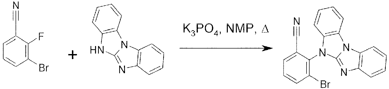
- A.) 15.0 g (75.0 mmol) 3-bromo-2-fluoro-benzonitrile, 15.5 g (75mmol) 6H-benzimidazolo[1,2-a]benzimidazole and 47.8 (225 mmol) potassium phosphate tribasic in 100 ml NMP (N-Methyl-2-pyrrolidon) are stirred at 105 °C under nitrogen for 3.5 h.
The reaction mixture is filtered hot and the organic phase is poured on water. The product is filtered of. Yield 26.4 g (91 %)
1H NMR (300 MHz, DMSO-D6): δ 8.37-8.41 (m, 1H), 8.27-8.32 (m, 3H), 7.83-7.88 (t, 1H, J=2*8Hz), 7.60-7.66 (m, 1H), 7.25-7.53 (m, 5H)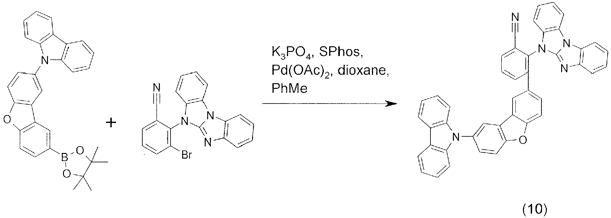
- B.) 5.00 g (12.9 mmol) 2-(benzimidazolo[1,2-a]benzimidazol-5-yl)-3-bromo-benzonitrile, 5.93 g (12.9 mmol) 9-[8-(4,4,5,5-tetramethyl-1,3,2-dioxaborolan-2-yl)dibenzofuran-2-yl]carbazole, 11.0 g (52.0 mmol) potassium phosphate tribasic in 32 ml dioxane, 80 ml toluene and 24 ml water are degased with argon. 0.1 g (0.5 mmol) palladium(II)acetate is added and the reaction mixture is degased with argon. 0.46 g (1 mmol) SPhos (2-Dicyclohexylphosphino-2',6'-dimethoxybiphenyl) is added and the reaction mixture is degased with argon. The reaction mixture is refluxed under argon for 18 h.
- The organic layer is washed with a 1 % solution of NaCN in water and then the organic phase is washed with water. The organic phase is dried with Magnesium sulfate and the solvent is removed in vacuum.
- Column chromatography on silica gel with dichloromethane gives 3 g 36 % of the product.
1H NMR (300 MHz, DMSO-D6): δ 7.98-8.32 (m, 9H), 7.87-7.90 (d, 1H), 7.67-7.70 (dd, 1H), 7.03-7.55 (m, 14H), -
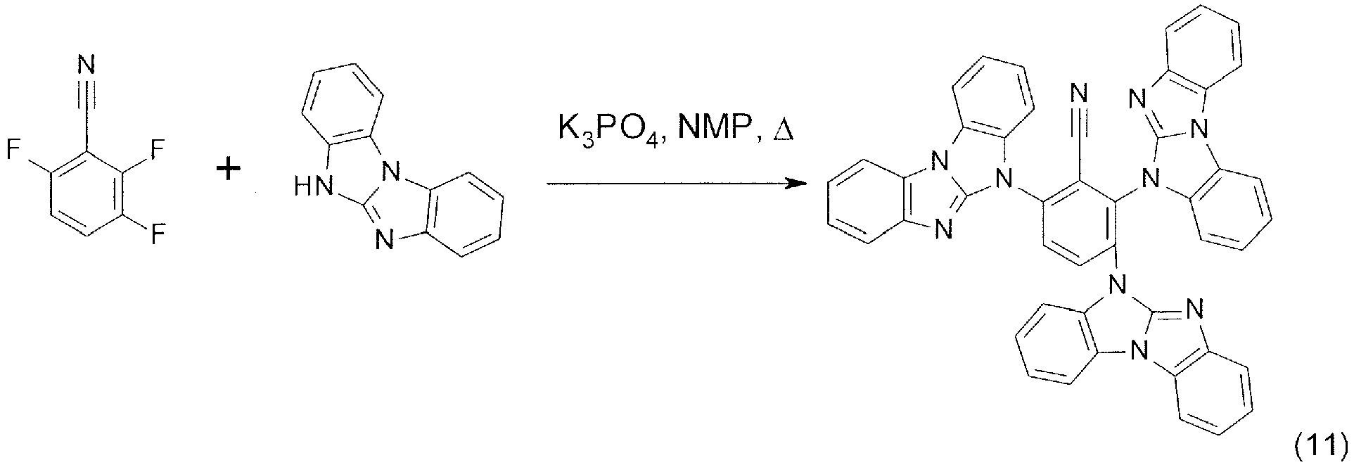
- 5.00 g (31.8 mmol) 3-bromo-2-fluoro-benzonitrile, 23.1 g (111 mmol) 6H-benzimidazolo[1,2-a]benzimidazole and 60.8 (0.286 mol) potassium phosphate tribasic in 120 ml NMP (N-Methyl-2-pyrrolidon) are stirred at 30 °C under nitrogen for 30 min. Then the reaction mixture is stierred at 120 °C for 4 h.
- The reaction mixture is filtered hot and is washing with water. The product is crystalized from DMSO. The product is filtered of. Yield 2.5 g (11 %)
1H NMR (300 MHz, DMSO-D6): δ 6.44-8.33 (m, 26H) -

- 2.5 g (15.9 mmol) 2,3,4-trifluorobenzonitrile, 10.9 g (52.5 mmol) 6H-benzimidazolo[1,2-a]benzimidazole and 27.0 g (0.127 mol) potassium phosphate tribasic in 50 ml NMP (N-Methyl-2-pyrrolidon) are stirred at 115 °C under nitrogen for 18 h. The reaction mixture is filtered hot and the organic phase is poured on water. The product is filtered of. Column chromatography on silica gel with chloroform gives 1.3 g (11.4 %) of the product.
1H NMR (300 MHz, DMSO-D6): rotamers: δ 8.55-8.82 (m, 2H); 6.41-8.07 (m, 24H)
MS (APCI(pos), m/z): 719 (M+1). -

- 4.0 g (28.8 mmol) 3,5-difluorobenzonitrile, 11.9 g (57.6 mmol) 6H-benzimidazolo[1,2-a]benzimidazole and 36.6 g (173 mmol) potassium phosphate tribasic in 50 ml NMP (N-Methyl-2-pyrrolidon) are stirred at 180°C under nitrogen for 7 h. The reaction mixture is filtered hot. Washing with water. Yield 6.6 g 47.7 % product.
1H NMR (400 MHz, TFA-d1): δ 8.87 (m, 1H); 8.70(s, 1H); 8.69 (s, 1H); 8.28 (d,J= 8.1 Hz 2H) 8.21 - 8.23 (m, 2H); 7.75-7.90 (m, 8H) -
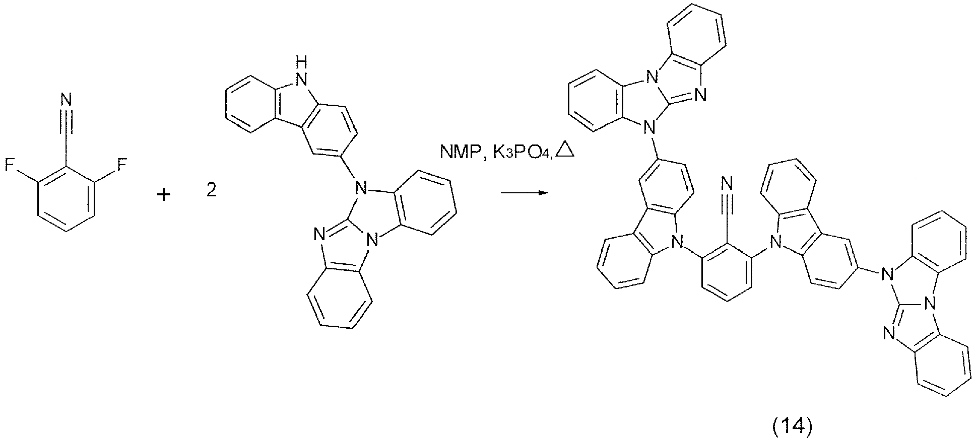
- 1.50 g (10.7 mmol) 2,6-difluorobenzonitrile, 8.19 g (22.0 mmol) 5-(9H-carbazol-3-yl)-5H-benzo[d]benzo[4,5]imidazo[1,2a]imidazole and 10.7 g (47.5 mmol) potassium phosphate tribasic in 30 ml NMP (N-Methyl-2-pyrrolidon) are stirred at 130°C under nitrogen for 7 h. The reaction mixture is filtered hot and the organic phase is poured on water. The product is filtered of. Column chromatography on silica gel with chloroform gives 4.7 g (51.6 %) of the product.
1H NMR (400 MHz, DMSO-D6): δ 8.80-8.81 (d, 2H), 8.38-8.45 (m, 3H), 8.21-8.32 (m, 6H), 8.01-8.03-7.50 (t, 1H), 7.99-8.00 (t, 1H), 7.82-7.83 (d, 1H), 7.80-7.81 (d, 1H), 7.59-7.65 (m, 8H), 7.27-7.48 (m, 10H) -
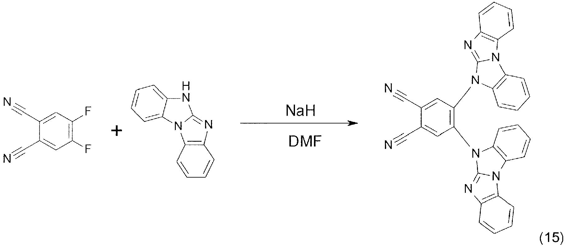
- 222mg NaH (60% in mineral oil) and 304 mg (1,85 mmol) 4,5-difluorophtalonitril is added to a solution of 960 mg (4.63 mmol) benzimidazolo[1,2-a]benzimidazole in 275 ml N,N-dimethylformamide and stirred 1,5 hours at room temperature. The reaction is quenched with 550 ml distilled water, the precipate is filtered, washed three times with distilled water, and dried under vacuum at 60 °C. The product is purified under chromatography using a 19:1 CH2Cl2 /THF mixture and obtained as a fine bright yellow powder (99.6% purity, 886 mg, 89% yield).
1H-NMR (DMSO; 500MHz): δ (ppm) 9,05 (d, 2H); 7,99 (d, 1H); 7,9 (m, 2H); 7,80 (d, 1H); 7,51 (d, 1H); 7,23 (m, 7H); 7,00 (m, 3H); 6,785 (t, 1H). -
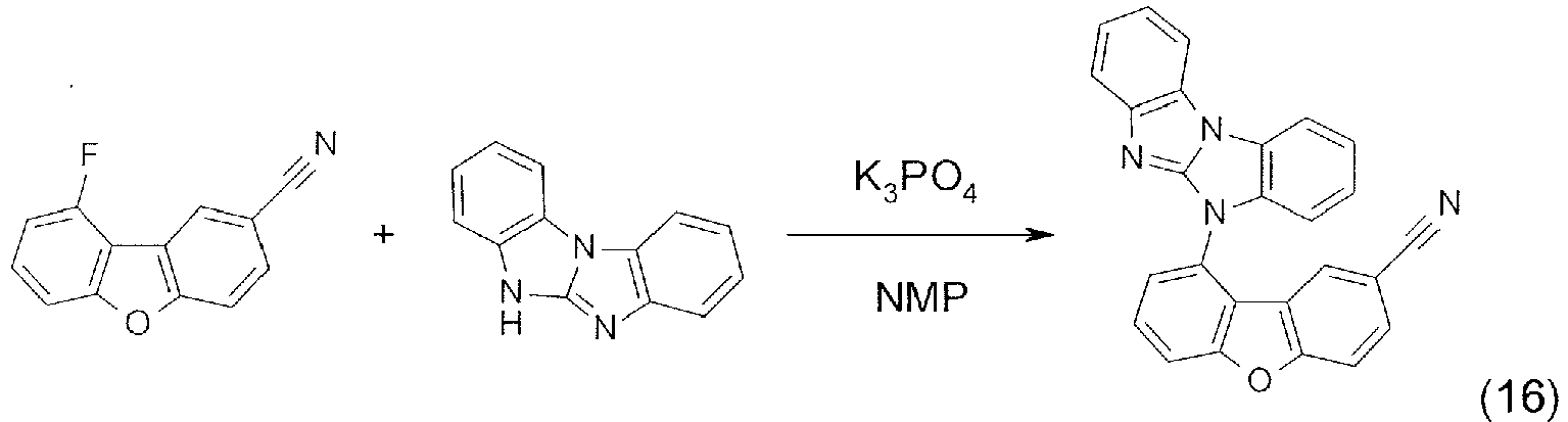
- 9-fluorodibenzofuran-2-carbonitrile (1.6 g, 7.58 mmol), 6H-benzimidazolo[1,2-a]benzimidazole (1.65 g, 7.96 mmol), and potassium phosphate (3.38 g, 15.91 mmol) are suspended in 39 mL of NMP, and the mixture is stirred at 185 °C for 14 h. After the reaction mixture is cooled at room temperature, it is diluted with 76 mL of water and 38 mL of EtOH. The solid is collected by filtration, and dried in vacuum oven at 50 °C. The crude product is purified by column chromatography on silica gel eluting with chloroform to yield 2.21 g (73%) of 9-(benzimidazolo[1,2-a]benzimidazol-5-yl)dibenzofuran-2-carbonitrileas a white solid.
1H-NMR (300 MHz, DMSO-d 6): δ 8.36-8.26 (m, 2H), 8.08-7.83 (m, 5H), 7.61-7.54 (m, 2H), 7.48 (td, J = 1.1, 7.8 Hz, 4H), 7.36-7.30 (m, 3H), 7.19 (d, J = 7.8 Hz, 1H) -

- A.) 10 g (50.0 mmol) 3-bromo-4-fluoro-benzonitrile, 9.33 g (45 mmol) 6H-benzimidazolo[1,2-a]benzimidazole and 31.8 g (150 mmol) K3PO4 are added to 100 ml DMF and the suspension is heated to 110°C for 23 h. The reaction mixture is filtered hot through Hyflo and the filtrate is evaporated on the rotavap to yield 18.6 g of crude product. The crude product is suspended in 100 ml MeOH, stirred at RT for 2h, filtered and dried at 80°C/125 mbar overnight to yield 15.1 g of a beige product. Recrystallization from 500 ml EtOAc yields
13.5 g (69.7% of theory) 2-(benzimidazolo[1,2-a]benzimidazol-5-yl)-3-bromo-benzonitrile as white solid.
1H-NMR (400 MHz, CDCl3): δ 8.08 (dxd, J1 = 8.4 Hz, J2 = 1.6 Hz, 1H), 7.90 - 7.865 (m, 3H), 7.76 (d, J = 7.6 Hz, 1H), 7.57 (t, J = 8.0 Hz, 1H), 7.44- 7.30 (m, 4H), 7.01 (d, J = 8.0 Hz,1H).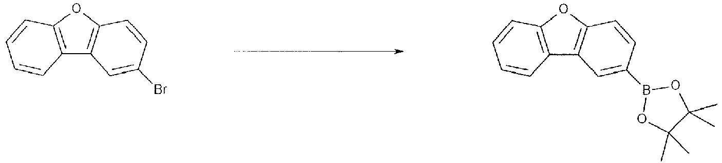
- B.) 40 g (160.3 mmol) 2-bromo-dibenzofuran are dissolved in 250 ml THF abs. and cooled to - 78°C. 65 ml (175.5 mmol) BuLi (2.7M in hexane) are added within 55 min while keeping the internal temperature below -73°C. The resulting suspension is stirred for 30 min followed by the addition of 33.5 g (176.3 mmol) 2-isopropoxy-4,4,5,5-tetramethyl-1,3,2-dioxaborolane within 30 min while keeping the internal temperature below -73°C. The reaction mixture is then slowly brought to RT, then 200 ml of buffer solution pH = 7 are added and the pH brought to 7 by the addition of HCl 4M. The organic solvent is then evaporated on the rotavap; the aqueous phase is extracted three times with EtOAc (250 ml each). The combined organic phases are washed three times with H2O (200 ml each), dried over Na2SO4, filtered and evaporated. The crude product (51.7 g) is purified by CombiFlash chromatography (solvent: Heptane / CH2Cl2 (0 to 40%)) to yield 34.1g of a colorless oil. 100 ml MeOH are added, the mixtue is heated to reflux, cooled to RT and then to 0°C. The suspension is filtered and the residue is dried at 30°C / 125 mbar overnight to yield 28.3 g (60.0% of theory) 2-dibenzofuran-2-yl-4,4,5,5-tetramethyl-1,3,2-dioxaborolane as a white solid.
1H-NMR (300 MHz, CDCl3): 8.45 (s (1H), 7.99 - 7.92 (m. 2H), 7.59 - 7.55 (m, 2H), 7.48 (t, J = 7.2 Hz, 1H), 7.37 (t, J = 7.8 Hz, 1H), 1.40 (s, 12H).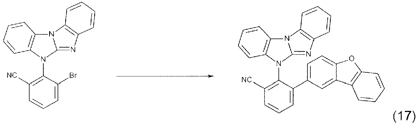
- C.) 7.68 g (19.8 mmol) 2-(benzimidazolo[1,2-a]benzimidazol-5-yl)-3-bromo-benzonitrile and 7.0 g (23.8 mmol) 2-dibenzofuran-2-yl-4,4,5,5-tetramethyl-1,3,2-dioxaborolane are dissolved in 140 ml THF and the solution is evacuated and purged three times with argon. 0.35 g (1.2 mmol) P(t-Bu)3 HBF4 and 0.54 g (0.6 mmol) Pd2(dba)3 are added and the solution is evacuated and purged three times with argon and heated to 50°C. A solution of 12.6 g (59.5 mmol) K3PO4 in 35 ml H2O (evacuated and purged three times with argon) is added with a syringe and the reaction mixture is heated to reflux for 17 h. To the cooled reaction mixture are added 300 ml EtOAc and the phases are separated. The organic phase is washed three times with brine (100 ml each), dried over MgSO4 filtered and evaporated on the rotavap to yield 13.3 g of crude product. Flash chromatography using CH2Cl2 / EtOAc = 9:1 as eluent
yields 7.23 g (68.0% of theory) 2-(benzimidazolo[1,2-a]benzimidazol-5-yl)-3-dibenzofuran-2-yl-benzonitrile as a white solid.
1H-NMR (300 MHz, CDCl3): δ 7.97 (m, 2H), 7.84 - 7.71 (m, 4H), 7.64 (d, J = 7.6 Hz, 1H), 7.53 (d, J = 8.0 Hz, 1H), 7.44 (d, J = 8.0 Hz, 1H), 7.39 - 7.33 (m, 2H), 7.28 - 7.11 (m, 6H), 6.90 (d, J = 7.6 Hz, 1H). -
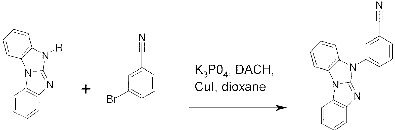
- A.) 20.0 g (87.3 mmol) 3-bromo-benzonitrile, 16.6 g (80.0 mmol) 6H-benzimidazolo[1,2-a]benzimidazole, 67.9 g (320 mmol) potassium phosphate tribasic, 1.5 g (7.88 mmol) cupper(I) iodide and 100 g (875 mmol) DACH ((±)-trans-1,2-diaminocyclohexane) in 240 ml dioxane are stirred at 100 °C under nitrogen for 7 h.
The reaction mixture is filtered hot and the solids are washed with dioxane. The reaction mixture is cooled to 50 °C and the crystalized product is filtered of and is washed with methanol. Yield 11.2 g (46 %)
1H-NMR (300 MHz, CDCl3): δ 7.33-7.49 (m, 4H), 7.59 - 7.63 (d, 1H), 7.72-7.83 (m, 3H), 7.86-7.90 (d, 2H), 8.22-8.26 (m, 2H),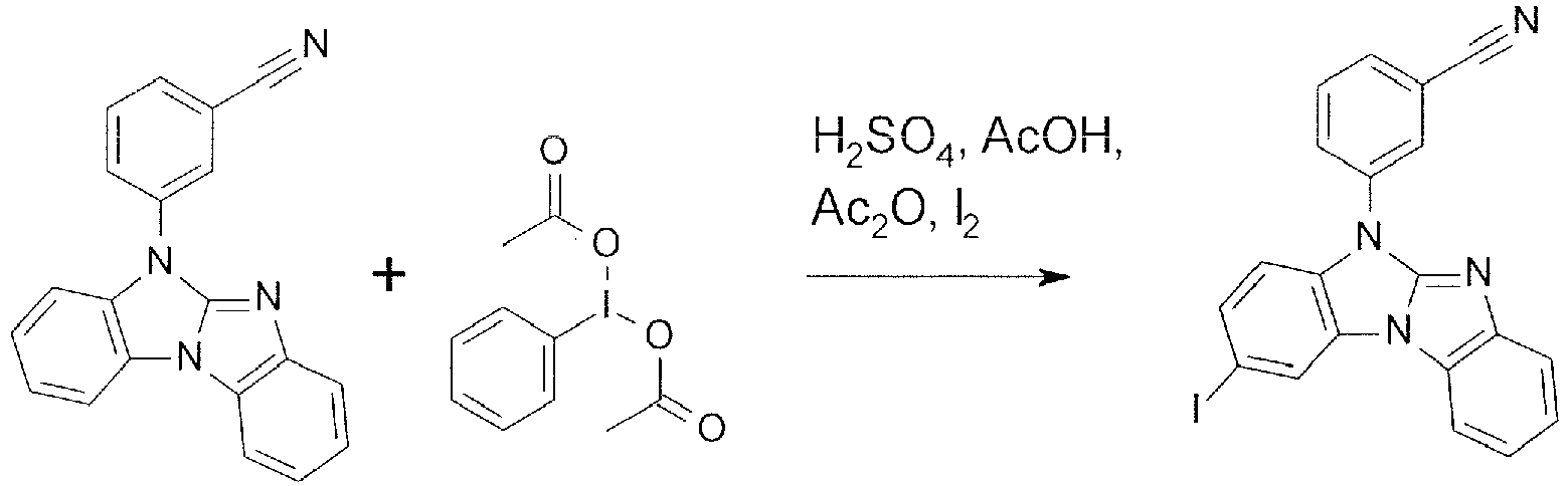
- B.) 11.2 g (36.3 mmol) 3-(benzimidazolo[1,2-a]benzimidazol-5-yl)benzonitrile, 11.7 g (36.3 mmol) diacetoxy-iodobenzene, 9.22 g (36.3 mmol) iodine in 90 ml acetic acid are stirred under nitrogen at 25 °C for 18 h. The product is filtered off and is washed with methanol and methanol water 95 to 5. Yield: 12.8 g (81 %)
1H-NMR (300 MHz, CDCl3): δ 7.39-7.61 (m, 4H), 7.66-7.70 (d, 1H), 7.73-7.86 (m, 3H), 8.18 - 8.23 (m, 3H)
- C.) To 10.0 g (20.7 mmol) 3-(2-iodobenzimidazolo[1,2-a]benzimidazol-5-yl)benzonitrile, 8.18 g (31.1 mmol) triphenylsilane, 17.6 g (82.9 mmol) potassium phosphate in 125 ml dimethylformamide is degassed with argon. 500 mg (1.131 mmol) Rhodium(II)-acetate is added and the reaction mixture is degassed with argon. The reaction mixture is stirred at 60 °C for 18 h under argon. 250 mg 500 mg (0.566 mmol) Rhodium(II)-acetate is added and the reaction mixture is stirred for 18 h under argon. The reaction is filtered and the filtrate is caped for crystallization. Colum chromatography with chloroform gives the product. Yield 1.5 g (12.8 %)
1H-NMR (300 MHz, CDCl3): δ 7.36-7.86 (m, 23H), 8.02 (s, 1H), 8.20-8.26 (m, 2H) - A glass substrate with 120 nm-thick indium-tin-oxide (ITO) transparent electrode used as an anode is first cleaned with isopropanol in an ultrasonic bath for 10 min. To eliminate any possible organic residues, the substrate is exposed to an ultraviolet light and ozone for further 30 min. This treatment also improves the hole injection properties of the ITO. The cleaned substrate is mounted on a substrate holder and loaded into a vacuum chamber. Thereafter, the organic materials specified below are applied by vapor deposition to the ITO substrate at a rate of approx. 0.2-1 Å/sec at about 10-6-10-8 mbar. As a hole injection layer, compound
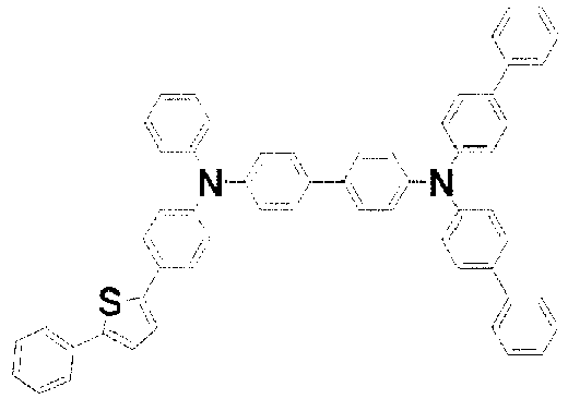
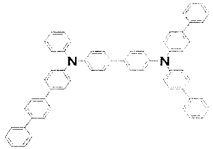

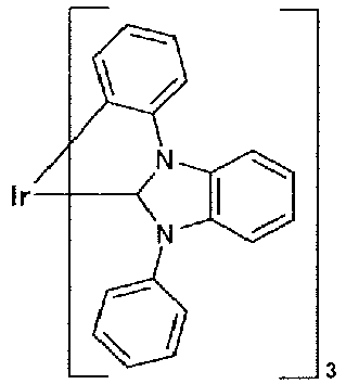
WO2005/019373 ) is then applied with a thickness of 10 nm. Subsequently, a mixture of 20% by weight of emitter compound,


- To characterize the OLED, electroluminescence spectra are recorded at various currents and voltages. In addition, the current-voltage characteristic is measured in combination with the luminance to determine luminous efficiency and external quantum efficiency (EQE). Driving voltage U and EQE are given at luminance (L) = 1000 cd/m2 except otherwise stated.
- Comparative Application Example 1 is repeated except that the host (SH-1) is replaced by compound
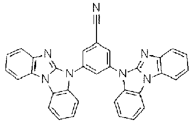
- Comparative Application Example 1 is repeated except that the host (SH-1) is replaced by compound
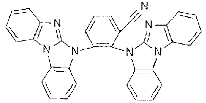
- Comparative Application Example 1 is repeated except that both the host (SH-1) and exciton blocker (SH-1) are replaced by compound
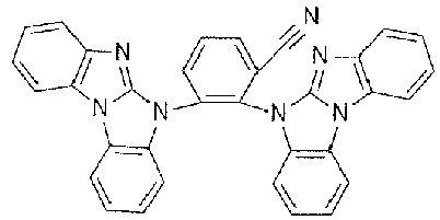
Table 1 Appl. Ex. Host Exciton blocker U [V] Luminous efficiency [lm/W] Comp. Appl. Ex. 1 (SH-1) (SH-1) 5.46 17.7 Appl. Ex. 1 (13) (SH-1) 4.83 19.3 Appl. Ex. 2 (5) (SH-1) 4.55 22.7 Appl. Ex. 3 (5) (5) 4.18 23.0 - The results shown in Table 1 demonstrate that the driving voltage U is significantly reduced with increasing luminous efficiency at the same time when compounds (5) or (13) is used as the host instead of reference compound (SH-1). Furthermore, when compound (5) is used as both the host and exciton blocker, the driving voltage U is further reduced and the luminous efficiency is also improved.
- A glass substrate with 120 nm-thick ITO is cleaned and treated in the same manner as comparative application example 1. As a hole injection layer, compound
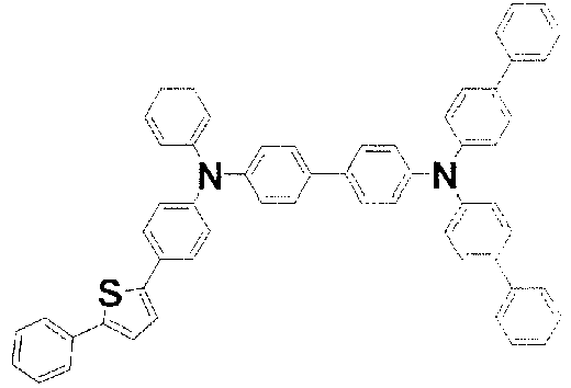

- Comparative Application Example 2 is repeated except that both the host (SH-1) and exciton blocker (SH-1) is replaced by compound
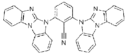
- Comparative Application Example 2 is repeated except that both the host (SH-1) and exciton blocker (SH-1) is replaced by compound
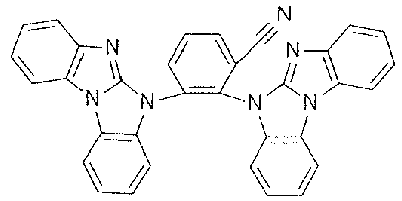
Table 2 Appl. Ex. Host Exciton blocker U [V] Luminous efficiency [lm/W] Comp. Appl. Ex. 2 (SH-1) (SH-1) 5.54 1.2 Appl. Ex. 4 (6) (6) 4.52 23.3 Appl. Ex. 5 (5) (5) 3.87 27.1 - The results shown in Table 2 demonstrate that the driving voltage and the luminous efficiency are improved when compounds (5) or (6) are used as host and exciton blocker instead of reference compound (SH-1).
Claims (8)
- A compound of formula (Ib),
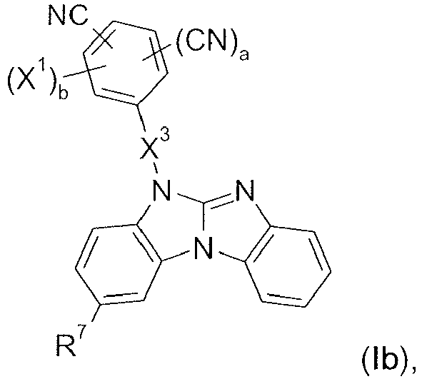 a is 0 or 1 and b is 0 or 1, whereby the sum of a and b is at least 1;X1 is a group of the following formula:

 X3 is a single bond, andR7 is H or group of the following formula:
 R70 and R71 are independently of each other a C1-C18alkyl group, a C6-C18aryl group, or a C6-C18aryl group, which is substituted by C1-C18alkyl, andR72 is a C1-C18alkyl group, a C6-C18aryl group, or a C6-C18aryl group, which is substituted by C1-C18alkyl.
 - An electronic device, comprising a compound according to claim 1.
- The electronic device according to claim 2, which is an electroluminescent device.
- A charge transport layer, a charge/exciton blocker layer, or an emitting layer comprising a compound according to claim 1.
- The emitting layer according to claim 4, comprising a compound according to claim 1 as host material.
- An apparatus selected from the group consisting of stationary visual display units; mobile visual display units; illumination units; keyboards; items of clothing; furniture; wallpaper, comprising the organic electronic device according to claim 2 or 3, or the charge transport layer, the charge/exciton blocker layer, or the emitting layer according to claim 4 or 5.
- Use of the compounds according to claim 1 in electrophotographic photoreceptors, photoelectric converters, organic solar cells, switching elements, organic light emitting field effect transistors, image sensors, dye lasers or electroluminescent devices.
- The emitting layer according to claim 4, comprising at least one compound of formula I as TADF emitter or as TADF host material in combination with at least one fluorescent emitter.
Priority Applications (3)
| Application Number | Priority Date | Filing Date | Title |
|---|---|---|---|
| EP15161950.9A EP3075737B1 (en) | 2015-03-31 | 2015-03-31 | Benzimidazolo[1,2-a]benzimidazole carrying aryl- or heteroarylnitril groups for organic light emitting diodes |
| PCT/IB2016/051831 WO2016157113A1 (en) | 2015-03-31 | 2016-03-31 | Benzimidazolo[1,2-a]benzimidazole carrying aryl- or heteroarylnitril groups for organic light emitting diodes |
| US15/563,072 US10689385B2 (en) | 2015-03-31 | 2016-03-31 | Benzimidazolo[1,2-A]benzimidazole carrying aryl- or arylnitril groups for organic light emitting diodes |
Applications Claiming Priority (1)
| Application Number | Priority Date | Filing Date | Title |
|---|---|---|---|
| EP15161950.9A EP3075737B1 (en) | 2015-03-31 | 2015-03-31 | Benzimidazolo[1,2-a]benzimidazole carrying aryl- or heteroarylnitril groups for organic light emitting diodes |
Publications (2)
| Publication Number | Publication Date |
|---|---|
| EP3075737A1 EP3075737A1 (en) | 2016-10-05 |
| EP3075737B1 true EP3075737B1 (en) | 2019-12-04 |
Family
ID=52811015
Family Applications (1)
| Application Number | Title | Priority Date | Filing Date |
|---|---|---|---|
| EP15161950.9A Active EP3075737B1 (en) | 2015-03-31 | 2015-03-31 | Benzimidazolo[1,2-a]benzimidazole carrying aryl- or heteroarylnitril groups for organic light emitting diodes |
Country Status (3)
| Country | Link |
|---|---|
| US (1) | US10689385B2 (en) |
| EP (1) | EP3075737B1 (en) |
| WO (1) | WO2016157113A1 (en) |
Families Citing this family (12)
| Publication number | Priority date | Publication date | Assignee | Title |
|---|---|---|---|---|
| CN108191870A (en) | 2012-07-10 | 2018-06-22 | Udc 爱尔兰有限责任公司 | For benzimidazole simultaneously [1,2-A] benzimidizole derivatives of electronic application |
| EP3034507A1 (en) * | 2014-12-15 | 2016-06-22 | Idemitsu Kosan Co., Ltd | 1-functionalized dibenzofurans and dibenzothiophenes for organic light emitting diodes (OLEDs) |
| US10608188B2 (en) * | 2017-09-11 | 2020-03-31 | Universal Display Corporation | Organic electroluminescent materials and devices |
| KR102172580B1 (en) * | 2018-02-13 | 2020-11-02 | 주식회사 엘지화학 | Heterocyclic compound and organic light emitting device comprising the same |
| EP3587423A1 (en) | 2018-06-27 | 2020-01-01 | Idemitsu Kosan Co., Ltd. | Organic compounds and an organic electroluminescence device comprising the same |
| WO2020022378A1 (en) | 2018-07-27 | 2020-01-30 | 出光興産株式会社 | Compound, material for organic electroluminescence element, organic electroluminescence element, and electronic device |
| EP3651225A1 (en) * | 2018-11-09 | 2020-05-13 | Idemitsu Kosan Co., Ltd. | Novel organic compounds and an organic electroluminescence device comprising the same |
| US11515489B2 (en) | 2018-11-28 | 2022-11-29 | Universal Display Corporation | Host materials for electroluminescent devices |
| CN109651406B (en) * | 2019-01-23 | 2021-01-08 | 苏州久显新材料有限公司 | Thermally activated delayed fluorescence compound, luminescent material and organic electroluminescent device |
| KR102721075B1 (en) * | 2019-02-15 | 2024-10-24 | 삼성전자주식회사 | Condensed cyclic compound and organic light emitting device comprising the same |
| US11512093B2 (en) | 2019-03-04 | 2022-11-29 | Universal Display Corporation | Compound used for organic light emitting device (OLED), consumer product and formulation |
| KR102739951B1 (en) | 2019-04-03 | 2024-12-06 | 삼성전자주식회사 | Condensed cyclic compound and organic light emitting device comprising the same |
Family Cites Families (159)
| Publication number | Priority date | Publication date | Assignee | Title |
|---|---|---|---|---|
| WO2000070655A2 (en) | 1999-05-13 | 2000-11-23 | The Trustees Of Princeton University | Very high efficiency organic light emitting devices based on electrophosphorescence |
| JP3924648B2 (en) | 1999-11-02 | 2007-06-06 | ソニー株式会社 | Organic electroluminescence device |
| KR100946314B1 (en) | 1999-12-01 | 2010-03-09 | 더 트러스티즈 오브 프린스턴 유니버시티 | Organic light emitting device comprising a phosphorescent organo metallic compound |
| US6821645B2 (en) | 1999-12-27 | 2004-11-23 | Fuji Photo Film Co., Ltd. | Light-emitting material comprising orthometalated iridium complex, light-emitting device, high efficiency red light-emitting device, and novel iridium complex |
| US6565994B2 (en) | 2000-02-10 | 2003-05-20 | Fuji Photo Film Co., Ltd. | Light emitting device material comprising iridium complex and light emitting device using same material |
| US20020121638A1 (en) | 2000-06-30 | 2002-09-05 | Vladimir Grushin | Electroluminescent iridium compounds with fluorinated phenylpyridines, phenylpyrimidines, and phenylquinolines and devices made with such compounds |
| US7306856B2 (en) | 2000-07-17 | 2007-12-11 | Fujifilm Corporation | Light-emitting element and iridium complex |
| CN101924190B (en) | 2000-08-11 | 2012-07-04 | 普林斯顿大学理事会 | Organometallic compounds and emission-shifting organic electrophosphorescence |
| JP4344494B2 (en) | 2000-08-24 | 2009-10-14 | 富士フイルム株式会社 | Light emitting device and novel polymer element |
| JP4067286B2 (en) | 2000-09-21 | 2008-03-26 | 富士フイルム株式会社 | Light emitting device and iridium complex |
| JP4154138B2 (en) | 2000-09-26 | 2008-09-24 | キヤノン株式会社 | Light emitting element, display device and metal coordination compound |
| JP4154139B2 (en) | 2000-09-26 | 2008-09-24 | キヤノン株式会社 | Light emitting element |
| JP4086499B2 (en) | 2000-11-29 | 2008-05-14 | キヤノン株式会社 | Metal coordination compound, light emitting device and display device |
| JP4154145B2 (en) | 2000-12-01 | 2008-09-24 | キヤノン株式会社 | Metal coordination compound, light emitting device and display device |
| DE10104426A1 (en) | 2001-02-01 | 2002-08-08 | Covion Organic Semiconductors | Process for the production of high-purity, tris-ortho-metallated organo-iridium compounds |
| JP4307000B2 (en) | 2001-03-08 | 2009-08-05 | キヤノン株式会社 | Metal coordination compound, electroluminescent element and display device |
| US6687266B1 (en) | 2002-11-08 | 2004-02-03 | Universal Display Corporation | Organic light emitting materials and devices |
| DE10338550A1 (en) | 2003-08-19 | 2005-03-31 | Basf Ag | Transition metal complexes with carbene ligands as emitters for organic light-emitting diodes (OLEDs) |
| WO2005113704A2 (en) | 2004-05-18 | 2005-12-01 | The University Of Southern California | Luminescent compounds with carbene ligands |
| US20060008670A1 (en) | 2004-07-06 | 2006-01-12 | Chun Lin | Organic light emitting materials and devices |
| TWI479008B (en) | 2004-07-07 | 2015-04-01 | Universal Display Corp | Stable and effective electroluminescent material |
| DE102004057072A1 (en) | 2004-11-25 | 2006-06-01 | Basf Ag | Use of Transition Metal Carbene Complexes in Organic Light Emitting Diodes (OLEDs) |
| CA2589711A1 (en) | 2004-12-23 | 2006-06-29 | Ciba Specialty Chemicals Holding Inc. | Electroluminescent metal complexes with nucleophilic carbene ligands |
| US8889266B2 (en) | 2005-03-17 | 2014-11-18 | Semiconductor Energy Laboratory Co., Ltd. | Organometallic complex, and light-emitting element, light-emitting device and electronic-device using the organometallic complex |
| DE102005014284A1 (en) | 2005-03-24 | 2006-09-28 | Basf Ag | Use of compounds containing aromatic or heteroaromatic rings containing groups via carbonyl groups as matrix materials in organic light-emitting diodes |
| GB2439030B (en) | 2005-04-18 | 2011-03-02 | Konica Minolta Holdings Inc | Organic electroluminescent device, display and illuminating device |
| TWI418606B (en) | 2005-04-25 | 2013-12-11 | Udc Ireland Ltd | Organic electroluminescent device |
| US8586204B2 (en) | 2007-12-28 | 2013-11-19 | Universal Display Corporation | Phosphorescent emitters and host materials with improved stability |
| US9051344B2 (en) | 2005-05-06 | 2015-06-09 | Universal Display Corporation | Stability OLED materials and devices |
| DE602006011734D1 (en) | 2005-05-30 | 2010-03-04 | Basf Se | ELECTROLUMINESCENT DEVICE |
| JP4887731B2 (en) | 2005-10-26 | 2012-02-29 | コニカミノルタホールディングス株式会社 | Organic electroluminescence element, display device and lighting device |
| DE502005009802D1 (en) | 2005-11-10 | 2010-08-05 | Novaled Ag | Doped organic semiconductor material |
| USRE44831E1 (en) | 2006-01-05 | 2014-04-08 | Konica Minolta Holdings, Inc. | Organic electroluminescent device, display, and illuminating device |
| KR101600624B1 (en) | 2006-02-10 | 2016-03-21 | 유니버셜 디스플레이 코포레이션 | METAL COMPLEXES OF CYCLOMETALLATED IMIDAZO[1,2-f]PHENANTHRIDINE AND DIIMIDAZO[1,2-A:1',2'-C]QUINAZOLINE LIGANDS AND ISOELECTRONIC AND BENZANNULATED ANALOGS THEREOF |
| US20090091253A1 (en) | 2006-03-17 | 2009-04-09 | Konica Minolta Holdings, Inc. | Organic electroluminescent element, display device and lighting device |
| ATE394800T1 (en) | 2006-03-21 | 2008-05-15 | Novaled Ag | HETEROCYCLIC RADICAL OR DIRADICAL, THEIR DIMERS, OLIGOMERS, POLYMERS, DISPIR COMPOUNDS AND POLYCYCLES, THEIR USE, ORGANIC SEMICONDUCTIVE MATERIAL AND ELECTRONIC COMPONENT |
| EP1837927A1 (en) | 2006-03-22 | 2007-09-26 | Novaled AG | Use of heterocyclic radicals for doping of organic semiconductors |
| EP2615153B1 (en) | 2006-03-23 | 2017-03-01 | Konica Minolta Holdings, Inc. | Organic electroluminescent device, display and illuminating device |
| US20070224446A1 (en) | 2006-03-24 | 2007-09-27 | Idemitsu Kosan Co., Ltd. | Material for organic electroluminescence device and organic electroluminescence device using the same |
| EP2001065B1 (en) | 2006-03-30 | 2016-11-09 | Konica Minolta Holdings, Inc. | Organic electroluminescent device, illuminating device and display device |
| KR20090007389A (en) | 2006-04-04 | 2009-01-16 | 바스프 에스이 | Transition metal complexes comprising one bicarbene ligand and one or two carbene ligands and their use in OLD |
| ATE550342T1 (en) | 2006-04-05 | 2012-04-15 | Basf Se | HETEROLEPTIC TRANSITION METAL-CARBEN COMPLEXES AND THEIR USE IN ORGANIC LIGHT-LIGHT DIODES (OLEDS) |
| JP5055818B2 (en) | 2006-04-19 | 2012-10-24 | コニカミノルタホールディングス株式会社 | ORGANIC ELECTROLUMINESCENT ELEMENT MATERIAL, ORGANIC ELECTROLUMINESCENT ELEMENT, DISPLAY DEVICE AND LIGHTING DEVICE |
| KR101453109B1 (en) | 2006-04-26 | 2014-10-27 | 이데미쓰 고산 가부시키가이샤 | Aromatic amine derivative, and organic electroluminescence element using the same |
| CN101461074B (en) | 2006-06-02 | 2011-06-15 | 出光兴产株式会社 | Material for organic electroluminescence element and organic electroluminescence element using same |
| JP2009541431A (en) | 2006-06-26 | 2009-11-26 | ビーエーエスエフ ソシエタス・ヨーロピア | Use of transition metal-carbene complexes without cyclometalation via non-carbene |
| JP2008021687A (en) | 2006-07-10 | 2008-01-31 | Mitsubishi Chemicals Corp | Organic electroluminescent element material, organic electroluminescent element composition, and organic electroluminescent element |
| WO2008022065A2 (en) | 2006-08-11 | 2008-02-21 | Light Prescriptions Innovators, Llc | Led luminance-enhancement and color-mixing by rotationally multiplexed beam-combining |
| JP5139297B2 (en) | 2006-08-23 | 2013-02-06 | 出光興産株式会社 | Aromatic amine derivatives and organic electroluminescence devices using them |
| JP2008066569A (en) | 2006-09-08 | 2008-03-21 | Konica Minolta Holdings Inc | Organic electroluminescence element, lighting system and display device |
| JP5332614B2 (en) | 2006-09-08 | 2013-11-06 | コニカミノルタ株式会社 | Organic electroluminescence element, lighting device and display device |
| WO2008029729A1 (en) | 2006-09-08 | 2008-03-13 | Konica Minolta Holdings, Inc. | Organic electroluminescent device, illuminating device and display |
| JP5556014B2 (en) | 2006-09-20 | 2014-07-23 | コニカミノルタ株式会社 | Organic electroluminescence device |
| US8241764B2 (en) | 2006-09-21 | 2012-08-14 | Basf Aktiengesellschaft | OLED display with extended lifetime |
| JP5589251B2 (en) | 2006-09-21 | 2014-09-17 | コニカミノルタ株式会社 | Organic electroluminescence element material |
| JP5011908B2 (en) | 2006-09-26 | 2012-08-29 | コニカミノルタホールディングス株式会社 | Organic electroluminescence element, display device and lighting device |
| JP5063992B2 (en) | 2006-11-20 | 2012-10-31 | ケミプロ化成株式会社 | Novel di (pyridylphenyl) derivative, electron transport material comprising the same, and organic electroluminescence device including the same |
| US8541112B2 (en) | 2006-12-13 | 2013-09-24 | Konica Minolta Holdings, Inc. | Organic electroluminescent element, display device and lighting device |
| WO2008090912A1 (en) | 2007-01-23 | 2008-07-31 | Konica Minolta Holdings, Inc. | Method for manufacturing organic electroluminescent device, organic electroluminescent device manufactured by the method, display device and illuminating device |
| JP2008207520A (en) | 2007-02-28 | 2008-09-11 | Konica Minolta Holdings Inc | Organic thin film, method for producing the same, electronic device, organic luminescence element, display device and lightening equipment |
| DE102007012794B3 (en) | 2007-03-16 | 2008-06-19 | Novaled Ag | Pyrido [3,2-h] quinazolines and / or their 5,6-dihydro derivatives, their method of preparation and doped organic semiconductor material containing them |
| EP3457451B1 (en) | 2007-04-30 | 2019-07-17 | Novaled GmbH | The use of oxocarbon, pseudooxocarbon and radialene compounds |
| US20100141126A1 (en) | 2007-05-16 | 2010-06-10 | Konica Minolta Holdings, Inc. | Organic electroluminescent element, display and illuminating device |
| WO2008146838A1 (en) | 2007-05-30 | 2008-12-04 | Konica Minolta Holdings, Inc. | Organic electroluminescent device, display device and illuminating device |
| WO2008156879A1 (en) | 2007-06-20 | 2008-12-24 | Universal Display Corporation | Blue phosphorescent imidazophenanthridine materials |
| JP5540701B2 (en) | 2007-06-21 | 2014-07-02 | コニカミノルタ株式会社 | Organic electroluminescence element material |
| US8373159B2 (en) | 2007-07-05 | 2013-02-12 | Basf Se | Organic light-emitting diodes comprising carbene-transition metal complex emitter, and at least one compound selected from disilylcarbazoles, disilyldibenzofurans, disilyldibenzothiophenes, disilyldibenzophospholes, disilyldibenzothiophene s-oxides and disilyldibe |
| EP3345983B1 (en) | 2007-07-05 | 2020-08-26 | UDC Ireland Limited | Compounds containing at least one disilyl compound selected from disilylcarbazoles, disilyldibenzofurans, disilyldibenzothiophenes, disilyldibenzophospholes, disilyldibenzothiophene s-oxides and disilyldibenzothiophene s, s-dioxides |
| TW200903877A (en) | 2007-07-10 | 2009-01-16 | Idemitsu Kosan Co | Material for organic electroluminescence device and organic electroluminescence device utilizing the same |
| JP5194596B2 (en) | 2007-07-11 | 2013-05-08 | コニカミノルタホールディングス株式会社 | Organic electroluminescence element, display device and lighting device |
| JP2009040728A (en) | 2007-08-09 | 2009-02-26 | Canon Inc | Organometallic complex and organic light emitting device using the same |
| JP5186843B2 (en) | 2007-08-30 | 2013-04-24 | コニカミノルタホールディングス株式会社 | Organic electroluminescence element, lighting device and display device |
| JP5624270B2 (en) | 2007-09-18 | 2014-11-12 | ユー・ディー・シー アイルランド リミテッド | Organic electroluminescence device |
| JP2011500648A (en) | 2007-10-17 | 2011-01-06 | ビーエーエスエフ ソシエタス・ヨーロピア | Transition metal complexes with bridged carbene ligands and their use in OLEDs |
| KR101612135B1 (en) | 2007-10-17 | 2016-04-12 | 바스프 에스이 | Transition metal complexes with bridged carbene ligands and use thereof in oleds |
| WO2009060757A1 (en) | 2007-11-08 | 2009-05-14 | Konica Minolta Holdings, Inc. | Organic electroluminescent device, display device and illuminating device |
| JP2009114369A (en) | 2007-11-08 | 2009-05-28 | Konica Minolta Holdings Inc | Organic electroluminescent material, organic electroluminescent element, display and illuminator |
| WO2009060779A1 (en) | 2007-11-08 | 2009-05-14 | Konica Minolta Holdings, Inc. | Organic electroluminescent device material, organic electroluminescent device, display device and illuminating device |
| JP2009114370A (en) | 2007-11-08 | 2009-05-28 | Konica Minolta Holdings Inc | Organic electroluminescence element material, organic electroluminescence element, display device, and lighting system |
| JP5458890B2 (en) | 2007-11-08 | 2014-04-02 | コニカミノルタ株式会社 | Organic electroluminescence element, display device and lighting device |
| WO2009060780A1 (en) | 2007-11-08 | 2009-05-14 | Konica Minolta Holdings, Inc. | Organic electroluminescence element, display device, and lighting system |
| JPWO2009063757A1 (en) | 2007-11-14 | 2011-03-31 | コニカミノルタホールディングス株式会社 | ORGANIC ELECTROLUMINESCENT ELEMENT MATERIAL, ORGANIC ELECTROLUMINESCENT ELEMENT, METHOD FOR PRODUCING ORGANIC ELECTROLUMINESCENT ELEMENT, DISPLAY DEVICE AND LIGHTING DEVICE |
| JP2009135183A (en) | 2007-11-29 | 2009-06-18 | Konica Minolta Holdings Inc | Organic electroluminescence element, display, and lighting device |
| WO2009073245A1 (en) | 2007-12-06 | 2009-06-11 | Universal Display Corporation | Light-emitting organometallic complexes |
| US20090153034A1 (en) | 2007-12-13 | 2009-06-18 | Universal Display Corporation | Carbazole-containing materials in phosphorescent light emittinig diodes |
| US8221905B2 (en) | 2007-12-28 | 2012-07-17 | Universal Display Corporation | Carbazole-containing materials in phosphorescent light emitting diodes |
| WO2009084413A1 (en) | 2007-12-28 | 2009-07-09 | Konica Minolta Holdings, Inc. | Organic electroluminescent device and method for manufacturing organic electroluminescent device |
| JP5549053B2 (en) | 2008-01-18 | 2014-07-16 | コニカミノルタ株式会社 | ORGANIC ELECTROLUMINESCENT ELEMENT MATERIAL, ORGANIC ELECTROLUMINESCENT ELEMENT, METHOD FOR PRODUCING ORGANIC ELECTROLUMINESCENT ELEMENT, DISPLAY DEVICE AND LIGHTING DEVICE |
| JP2009182298A (en) | 2008-02-01 | 2009-08-13 | Konica Minolta Holdings Inc | Organic electroluminescence element, lighting device, and display device |
| WO2009104488A1 (en) | 2008-02-20 | 2009-08-27 | コニカミノルタホールディングス株式会社 | White light-emitting organic electroluminescent device |
| JP2009267255A (en) | 2008-04-28 | 2009-11-12 | Idemitsu Kosan Co Ltd | Material for organic electroluminescent element and organic electroluminescent element using the material |
| US8057712B2 (en) | 2008-04-29 | 2011-11-15 | Novaled Ag | Radialene compounds and their use |
| EP2479234B1 (en) | 2008-05-13 | 2017-06-21 | Konica Minolta Holdings, Inc. | Organic electroluminescent element, display device and lighting device |
| CN102131891B (en) | 2008-06-30 | 2014-01-29 | 通用显示公司 | Hole transport materials having a sulfur-containing group |
| US8440326B2 (en) | 2008-06-30 | 2013-05-14 | Universal Display Corporation | Hole transport materials containing triphenylene |
| JP5533652B2 (en) | 2008-07-01 | 2014-06-25 | コニカミノルタ株式会社 | White light-emitting organic electroluminescence element, lighting device and display device |
| JP2010021336A (en) | 2008-07-10 | 2010-01-28 | Konica Minolta Holdings Inc | Organic electroluminescence device, illuminator, and display device |
| JP5609641B2 (en) | 2008-07-10 | 2014-10-22 | コニカミノルタ株式会社 | Organic electroluminescence element, display device and lighting device |
| JP5338184B2 (en) | 2008-08-06 | 2013-11-13 | コニカミノルタ株式会社 | Organic electroluminescence element, display device, lighting device |
| JPWO2010024404A1 (en) | 2008-08-28 | 2012-01-26 | 旭硝子株式会社 | Polishing composition and method for manufacturing semiconductor integrated circuit device |
| WO2010027583A1 (en) | 2008-09-03 | 2010-03-11 | Universal Display Corporation | Phosphorescent materials |
| JP5661635B2 (en) | 2008-10-07 | 2015-01-28 | オスラム オプト セミコンダクターズ ゲゼルシャフト ミット ベシュレンクテル ハフツングOsram Opto Semiconductors GmbH | Siloles substituted with fused ring systems and their use in organic electronics |
| WO2010044342A1 (en) | 2008-10-15 | 2010-04-22 | コニカミノルタホールディングス株式会社 | Organic el element, organic el element manufacturing method, white organic el element, display device, and illumination device |
| ES2370120T3 (en) | 2008-10-23 | 2011-12-12 | Novaled Ag | RADIALENE COMPOUND AND ITS USE. |
| JP5493333B2 (en) | 2008-11-05 | 2014-05-14 | コニカミノルタ株式会社 | ORGANIC ELECTROLUMINESCENT ELEMENT, WHITE ORGANIC ELECTROLUMINESCENT ELEMENT, DISPLAY DEVICE AND LIGHTING DEVICE |
| EP2362889B1 (en) | 2008-11-11 | 2018-12-26 | Universal Display Corporation | Phosphorescent emitters |
| JP5707665B2 (en) | 2008-12-03 | 2015-04-30 | コニカミノルタ株式会社 | ORGANIC ELECTROLUMINESCENCE ELEMENT, LIGHTING DEVICE AND DISPLAY DEVICE HAVING THE ELEMENT |
| WO2010067746A1 (en) | 2008-12-08 | 2010-06-17 | コニカミノルタホールディングス株式会社 | Organic electroluminescence element, display device and illumination device |
| US8815415B2 (en) | 2008-12-12 | 2014-08-26 | Universal Display Corporation | Blue emitter with high efficiency based on imidazo[1,2-f] phenanthridine iridium complexes |
| US9458182B2 (en) | 2009-01-07 | 2016-10-04 | Basf Se | Silyl- and heteroatom-substituted compounds selected from carbazoles, dibenzofurans, dibenzothiophenes and dibenzophospholes, and use thereof in organic electronics |
| JP5810529B2 (en) | 2009-01-09 | 2015-11-11 | コニカミノルタ株式会社 | Organic electroluminescence element, display device and lighting device |
| JP5472121B2 (en) | 2009-01-28 | 2014-04-16 | コニカミノルタ株式会社 | ORGANIC ELECTROLUMINESCENT ELEMENT, DISPLAY DEVICE AND LIGHTING DEVICE, AND METHOD FOR PRODUCING ORGANIC ELECTROLUMINESCENT ELEMENT |
| DE102009007038A1 (en) | 2009-02-02 | 2010-08-05 | Merck Patent Gmbh | metal complexes |
| EP3046156A1 (en) | 2009-02-06 | 2016-07-20 | Konica Minolta Holdings, Inc. | Organic electroluminescent element, and illumination device and display device each comprising the element |
| WO2010095564A1 (en) | 2009-02-18 | 2010-08-26 | コニカミノルタホールディングス株式会社 | Organic electroluminescent element, and illuminating device and display device each comprising the element |
| US8592806B2 (en) | 2009-02-26 | 2013-11-26 | Novaled Ag | Quinone compounds as dopants in organic electronics |
| US8709615B2 (en) | 2011-07-28 | 2014-04-29 | Universal Display Corporation | Heteroleptic iridium complexes as dopants |
| EP2417215B1 (en) | 2009-04-06 | 2014-05-07 | Universal Display Corporation | Metal complex comprising novel ligand structures |
| EP2246862A1 (en) | 2009-04-27 | 2010-11-03 | Novaled AG | Organic electronic device comprising an organic semiconducting material |
| TWI687408B (en) | 2009-04-28 | 2020-03-11 | 美商環球展覽公司 | Iridium complex with methyl-D3 substitution |
| US8603642B2 (en) | 2009-05-13 | 2013-12-10 | Global Oled Technology Llc | Internal connector for organic electronic devices |
| KR101986469B1 (en) | 2009-10-28 | 2019-06-05 | 유디씨 아일랜드 리미티드 | Heteroleptic carbene complexes and the use thereof in organic electronics |
| WO2011073149A1 (en) | 2009-12-14 | 2011-06-23 | Basf Se | Metal complexes comprising diazabenzimidazol carbene-ligands and the use thereof in oleds |
| US8288187B2 (en) | 2010-01-20 | 2012-10-16 | Universal Display Corporation | Electroluminescent devices for lighting applications |
| US9156870B2 (en) | 2010-02-25 | 2015-10-13 | Universal Display Corporation | Phosphorescent emitters |
| EP2363398B1 (en) | 2010-03-01 | 2017-10-18 | Semiconductor Energy Laboratory Co., Ltd. | Heterocyclic compound, light-emitting element, light-emitting device, electronic device, and lighting device |
| US9175211B2 (en) | 2010-03-03 | 2015-11-03 | Universal Display Corporation | Phosphorescent materials |
| US8334545B2 (en) | 2010-03-24 | 2012-12-18 | Universal Display Corporation | OLED display architecture |
| US8227801B2 (en) | 2010-04-26 | 2012-07-24 | Universal Display Corporation | Bicarbzole containing compounds for OLEDs |
| KR101877581B1 (en) | 2010-06-18 | 2018-07-11 | 유디씨 아일랜드 리미티드 | Organic electronic devices comprising a layer of a pyridine compound and a 8-hydroxyquinolinolato earth alkaline metal, or alkali metal complex |
| JP5990515B2 (en) | 2010-06-18 | 2016-09-14 | ビーエーエスエフ ソシエタス・ヨーロピアBasf Se | Organic electronic device comprising a layer of a dibenzofuran compound and an 8-hydroxyquinolinolato alkaline earth metal complex or an 8-hydroxyquinolinolato alkali metal complex |
| DE102010024542A1 (en) | 2010-06-22 | 2011-12-22 | Merck Patent Gmbh | Materials for electronic devices |
| RU2452872C2 (en) | 2010-07-15 | 2012-06-10 | Андрей Леонидович Кузнецов | Piezoelectric pump |
| WO2012014621A1 (en) | 2010-07-29 | 2012-02-02 | コニカミノルタホールディングス株式会社 | Transparent conductive film and organic electroluminescent element |
| ES2386564B1 (en) | 2010-08-06 | 2013-04-26 | Telefónica, S.A. | METHOD FOR MANAGING PRESENCE INFORMATION. |
| US8932734B2 (en) | 2010-10-08 | 2015-01-13 | Universal Display Corporation | Organic electroluminescent materials and devices |
| KR102071726B1 (en) | 2010-10-22 | 2020-01-30 | 가부시키가이샤 한도오따이 에네루기 켄큐쇼 | Organometallic complex, light-emitting element, light-emitting device, electronic device and lighting device |
| JP5900351B2 (en) | 2011-02-02 | 2016-04-06 | コニカミノルタ株式会社 | Method for manufacturing organic electroluminescence element |
| WO2012111462A1 (en) | 2011-02-15 | 2012-08-23 | コニカミノルタホールディングス株式会社 | Organic electroluminescence element and illumination device |
| JP5839027B2 (en) | 2011-02-22 | 2016-01-06 | コニカミノルタ株式会社 | ORGANIC ELECTROLUMINESCENCE ELEMENT, ITS MANUFACTURING METHOD, LIGHTING DEVICE, AND DISPLAY DEVICE |
| US8883322B2 (en) | 2011-03-08 | 2014-11-11 | Universal Display Corporation | Pyridyl carbene phosphorescent emitters |
| CN114315840A (en) | 2011-03-25 | 2022-04-12 | Udc 爱尔兰有限责任公司 | 4H-imidazo [1,2-a ] imidazoles for electronic applications |
| WO2012147397A1 (en) | 2011-04-26 | 2012-11-01 | コニカミノルタホールディングス株式会社 | Organic electroluminescent element and illuminating apparatus |
| US9212197B2 (en) | 2011-05-19 | 2015-12-15 | Universal Display Corporation | Phosphorescent heteroleptic phenylbenzimidazole dopants |
| US8748012B2 (en) | 2011-05-25 | 2014-06-10 | Universal Display Corporation | Host materials for OLED |
| US10079349B2 (en) | 2011-05-27 | 2018-09-18 | Universal Display Corporation | Organic electroluminescent materials and devices |
| KR20120135363A (en) | 2011-06-01 | 2012-12-13 | 엘지디스플레이 주식회사 | Blue phosphorescent compound and organic electroluminescence device using the same |
| KR102119353B1 (en) | 2011-06-08 | 2020-06-29 | 유니버셜 디스플레이 코포레이션 | Heteroleptic iridium carbene complexes and light emitting device using them |
| CN107501330A (en) | 2011-06-14 | 2017-12-22 | Udc 爱尔兰有限责任公司 | Metal complex comprising azabenzimidazoles carbene ligands and its purposes in OLED |
| US8409729B2 (en) | 2011-07-28 | 2013-04-02 | Universal Display Corporation | Host materials for phosphorescent OLEDs |
| US9705092B2 (en) | 2011-08-05 | 2017-07-11 | Universal Display Corporation | Phosphorescent organic light emitting devices combined with hole transport material having high operating stability |
| CN108299439B (en) | 2011-11-10 | 2021-02-09 | Udc 爱尔兰有限责任公司 | 4H-imidazo [1,2-a ] imidazoles for electronic applications |
| CN103959503B (en) * | 2011-12-05 | 2016-08-24 | 出光兴产株式会社 | Material for organic electroluminescent element and organic electroluminescent element |
| JP2014135466A (en) | 2012-04-09 | 2014-07-24 | Kyushu Univ | Organic light emitting element, and light emitting material and compound used in the same |
| JP5954411B2 (en) | 2012-04-10 | 2016-07-20 | 株式会社Ihi | Turbocharger |
| CN108191870A (en) | 2012-07-10 | 2018-06-22 | Udc 爱尔兰有限责任公司 | For benzimidazole simultaneously [1,2-A] benzimidizole derivatives of electronic application |
| CN104662023B (en) | 2012-09-20 | 2017-08-18 | Udc 爱尔兰有限责任公司 | Azadibenzofurans for electron applications |
| EP3034507A1 (en) | 2014-12-15 | 2016-06-22 | Idemitsu Kosan Co., Ltd | 1-functionalized dibenzofurans and dibenzothiophenes for organic light emitting diodes (OLEDs) |
| EP3034506A1 (en) | 2014-12-15 | 2016-06-22 | Idemitsu Kosan Co., Ltd | 4-functionalized carbazole derivatives for electronic applications |
-
2015
- 2015-03-31 EP EP15161950.9A patent/EP3075737B1/en active Active
-
2016
- 2016-03-31 US US15/563,072 patent/US10689385B2/en active Active
- 2016-03-31 WO PCT/IB2016/051831 patent/WO2016157113A1/en not_active Ceased
Non-Patent Citations (1)
| Title |
|---|
| None * |
Also Published As
| Publication number | Publication date |
|---|---|
| WO2016157113A1 (en) | 2016-10-06 |
| US20180086763A1 (en) | 2018-03-29 |
| EP3075737A1 (en) | 2016-10-05 |
| US10689385B2 (en) | 2020-06-23 |
Similar Documents
| Publication | Publication Date | Title |
|---|---|---|
| US11744152B2 (en) | Benzimidazo[1,2-a]benzimidazole derivatives for electronic applications | |
| EP3075737B1 (en) | Benzimidazolo[1,2-a]benzimidazole carrying aryl- or heteroarylnitril groups for organic light emitting diodes | |
| EP3119770B1 (en) | New dibenzofurans and dibenzothiophenes | |
| EP2776443B1 (en) | 4h-imidazo[1,2-a]imidazoles for electronic applications | |
| EP3072943B1 (en) | Dibenzofuran/carbazole-substituted benzonitriles | |
| EP3174885B1 (en) | 2,9-functionalized benzimidazolo[1,2-a]benzimidazoles as hosts for organic light emitting diodes (oleds) | |
| EP3034507A1 (en) | 1-functionalized dibenzofurans and dibenzothiophenes for organic light emitting diodes (OLEDs) | |
| US11174258B2 (en) | Benzimidazolo[1,2-a]benzimidazole derivatives for organic light emitting diodes | |
| EP3356368B1 (en) | Benzimidazolo[1,2-a]benzimidazole carrying benzimidazolo[1,2-a]benzimidazolyl groups, carbazolyl groups, benzofurane groups or benzothiophene groups for organic light emitting diodes | |
| US20180277768A1 (en) | Benzimidazolo[1,2-a]benzimidazole carrying benzimidazolo[1,2-a]benzimidazolyl groups, carbazolyl groups, dibenzofurane groups or benzothiophene groups for organic light emitting diodes | |
| EP3070144B1 (en) | Seven-membered ring compounds | |
| EP3034506A1 (en) | 4-functionalized carbazole derivatives for electronic applications | |
| EP3356369B1 (en) | Benzimidazolo[1,2-a]benzimidazole carrying triazine groups for organic light emitting diodes | |
| US10968229B2 (en) | Seven-membered ring compounds | |
| EP3061759B1 (en) | Nitrile substituted dibenzofurans | |
| WO2016079667A1 (en) | Indole derivatives for electronic applications | |
| WO2016067261A1 (en) | 5-((benz)imidazol-2-yl)benzimidazo[1,2-a]benzimidazoles for electronic applications |
Legal Events
| Date | Code | Title | Description |
|---|---|---|---|
| PUAI | Public reference made under article 153(3) epc to a published international application that has entered the european phase |
Free format text: ORIGINAL CODE: 0009012 |
|
| AK | Designated contracting states |
Kind code of ref document: A1 Designated state(s): AL AT BE BG CH CY CZ DE DK EE ES FI FR GB GR HR HU IE IS IT LI LT LU LV MC MK MT NL NO PL PT RO RS SE SI SK SM TR |
|
| AX | Request for extension of the european patent |
Extension state: BA ME |
|
| STAA | Information on the status of an ep patent application or granted ep patent |
Free format text: STATUS: REQUEST FOR EXAMINATION WAS MADE |
|
| 17P | Request for examination filed |
Effective date: 20170404 |
|
| RBV | Designated contracting states (corrected) |
Designated state(s): AL AT BE BG CH CY CZ DE DK EE ES FI FR GB GR HR HU IE IS IT LI LT LU LV MC MK MT NL NO PL PT RO RS SE SI SK SM TR |
|
| STAA | Information on the status of an ep patent application or granted ep patent |
Free format text: STATUS: EXAMINATION IS IN PROGRESS |
|
| 17Q | First examination report despatched |
Effective date: 20170725 |
|
| GRAP | Despatch of communication of intention to grant a patent |
Free format text: ORIGINAL CODE: EPIDOSNIGR1 |
|
| STAA | Information on the status of an ep patent application or granted ep patent |
Free format text: STATUS: GRANT OF PATENT IS INTENDED |
|
| INTG | Intention to grant announced |
Effective date: 20190116 |
|
| GRAS | Grant fee paid |
Free format text: ORIGINAL CODE: EPIDOSNIGR3 |
|
| GRAJ | Information related to disapproval of communication of intention to grant by the applicant or resumption of examination proceedings by the epo deleted |
Free format text: ORIGINAL CODE: EPIDOSDIGR1 |
|
| GRAL | Information related to payment of fee for publishing/printing deleted |
Free format text: ORIGINAL CODE: EPIDOSDIGR3 |
|
| STAA | Information on the status of an ep patent application or granted ep patent |
Free format text: STATUS: EXAMINATION IS IN PROGRESS |
|
| GRAP | Despatch of communication of intention to grant a patent |
Free format text: ORIGINAL CODE: EPIDOSNIGR1 |
|
| STAA | Information on the status of an ep patent application or granted ep patent |
Free format text: STATUS: GRANT OF PATENT IS INTENDED |
|
| INTC | Intention to grant announced (deleted) | ||
| INTG | Intention to grant announced |
Effective date: 20190903 |
|
| GRAA | (expected) grant |
Free format text: ORIGINAL CODE: 0009210 |
|
| STAA | Information on the status of an ep patent application or granted ep patent |
Free format text: STATUS: THE PATENT HAS BEEN GRANTED |
|
| AK | Designated contracting states |
Kind code of ref document: B1 Designated state(s): AL AT BE BG CH CY CZ DE DK EE ES FI FR GB GR HR HU IE IS IT LI LT LU LV MC MK MT NL NO PL PT RO RS SE SI SK SM TR |
|
| REG | Reference to a national code |
Ref country code: GB Ref legal event code: FG4D |
|
| REG | Reference to a national code |
Ref country code: CH Ref legal event code: EP |
|
| REG | Reference to a national code |
Ref country code: AT Ref legal event code: REF Ref document number: 1209265 Country of ref document: AT Kind code of ref document: T Effective date: 20191215 |
|
| REG | Reference to a national code |
Ref country code: DE Ref legal event code: R096 Ref document number: 602015042808 Country of ref document: DE |
|
| REG | Reference to a national code |
Ref country code: IE Ref legal event code: FG4D |
|
| REG | Reference to a national code |
Ref country code: NL Ref legal event code: MP Effective date: 20191204 |
|
| REG | Reference to a national code |
Ref country code: LT Ref legal event code: MG4D |
|
| PG25 | Lapsed in a contracting state [announced via postgrant information from national office to epo] |
Ref country code: SE Free format text: LAPSE BECAUSE OF FAILURE TO SUBMIT A TRANSLATION OF THE DESCRIPTION OR TO PAY THE FEE WITHIN THE PRESCRIBED TIME-LIMIT Effective date: 20191204 Ref country code: LV Free format text: LAPSE BECAUSE OF FAILURE TO SUBMIT A TRANSLATION OF THE DESCRIPTION OR TO PAY THE FEE WITHIN THE PRESCRIBED TIME-LIMIT Effective date: 20191204 Ref country code: NO Free format text: LAPSE BECAUSE OF FAILURE TO SUBMIT A TRANSLATION OF THE DESCRIPTION OR TO PAY THE FEE WITHIN THE PRESCRIBED TIME-LIMIT Effective date: 20200304 Ref country code: GR Free format text: LAPSE BECAUSE OF FAILURE TO SUBMIT A TRANSLATION OF THE DESCRIPTION OR TO PAY THE FEE WITHIN THE PRESCRIBED TIME-LIMIT Effective date: 20200305 Ref country code: LT Free format text: LAPSE BECAUSE OF FAILURE TO SUBMIT A TRANSLATION OF THE DESCRIPTION OR TO PAY THE FEE WITHIN THE PRESCRIBED TIME-LIMIT Effective date: 20191204 Ref country code: FI Free format text: LAPSE BECAUSE OF FAILURE TO SUBMIT A TRANSLATION OF THE DESCRIPTION OR TO PAY THE FEE WITHIN THE PRESCRIBED TIME-LIMIT Effective date: 20191204 Ref country code: BG Free format text: LAPSE BECAUSE OF FAILURE TO SUBMIT A TRANSLATION OF THE DESCRIPTION OR TO PAY THE FEE WITHIN THE PRESCRIBED TIME-LIMIT Effective date: 20200304 |
|
| PG25 | Lapsed in a contracting state [announced via postgrant information from national office to epo] |
Ref country code: RS Free format text: LAPSE BECAUSE OF FAILURE TO SUBMIT A TRANSLATION OF THE DESCRIPTION OR TO PAY THE FEE WITHIN THE PRESCRIBED TIME-LIMIT Effective date: 20191204 Ref country code: HR Free format text: LAPSE BECAUSE OF FAILURE TO SUBMIT A TRANSLATION OF THE DESCRIPTION OR TO PAY THE FEE WITHIN THE PRESCRIBED TIME-LIMIT Effective date: 20191204 |
|
| PG25 | Lapsed in a contracting state [announced via postgrant information from national office to epo] |
Ref country code: AL Free format text: LAPSE BECAUSE OF FAILURE TO SUBMIT A TRANSLATION OF THE DESCRIPTION OR TO PAY THE FEE WITHIN THE PRESCRIBED TIME-LIMIT Effective date: 20191204 |
|
| PG25 | Lapsed in a contracting state [announced via postgrant information from national office to epo] |
Ref country code: PT Free format text: LAPSE BECAUSE OF FAILURE TO SUBMIT A TRANSLATION OF THE DESCRIPTION OR TO PAY THE FEE WITHIN THE PRESCRIBED TIME-LIMIT Effective date: 20200429 Ref country code: EE Free format text: LAPSE BECAUSE OF FAILURE TO SUBMIT A TRANSLATION OF THE DESCRIPTION OR TO PAY THE FEE WITHIN THE PRESCRIBED TIME-LIMIT Effective date: 20191204 Ref country code: ES Free format text: LAPSE BECAUSE OF FAILURE TO SUBMIT A TRANSLATION OF THE DESCRIPTION OR TO PAY THE FEE WITHIN THE PRESCRIBED TIME-LIMIT Effective date: 20191204 Ref country code: CZ Free format text: LAPSE BECAUSE OF FAILURE TO SUBMIT A TRANSLATION OF THE DESCRIPTION OR TO PAY THE FEE WITHIN THE PRESCRIBED TIME-LIMIT Effective date: 20191204 Ref country code: RO Free format text: LAPSE BECAUSE OF FAILURE TO SUBMIT A TRANSLATION OF THE DESCRIPTION OR TO PAY THE FEE WITHIN THE PRESCRIBED TIME-LIMIT Effective date: 20191204 Ref country code: NL Free format text: LAPSE BECAUSE OF FAILURE TO SUBMIT A TRANSLATION OF THE DESCRIPTION OR TO PAY THE FEE WITHIN THE PRESCRIBED TIME-LIMIT Effective date: 20191204 |
|
| PG25 | Lapsed in a contracting state [announced via postgrant information from national office to epo] |
Ref country code: IS Free format text: LAPSE BECAUSE OF FAILURE TO SUBMIT A TRANSLATION OF THE DESCRIPTION OR TO PAY THE FEE WITHIN THE PRESCRIBED TIME-LIMIT Effective date: 20200404 Ref country code: SK Free format text: LAPSE BECAUSE OF FAILURE TO SUBMIT A TRANSLATION OF THE DESCRIPTION OR TO PAY THE FEE WITHIN THE PRESCRIBED TIME-LIMIT Effective date: 20191204 Ref country code: SM Free format text: LAPSE BECAUSE OF FAILURE TO SUBMIT A TRANSLATION OF THE DESCRIPTION OR TO PAY THE FEE WITHIN THE PRESCRIBED TIME-LIMIT Effective date: 20191204 |
|
| REG | Reference to a national code |
Ref country code: DE Ref legal event code: R097 Ref document number: 602015042808 Country of ref document: DE |
|
| REG | Reference to a national code |
Ref country code: AT Ref legal event code: MK05 Ref document number: 1209265 Country of ref document: AT Kind code of ref document: T Effective date: 20191204 |
|
| PLBE | No opposition filed within time limit |
Free format text: ORIGINAL CODE: 0009261 |
|
| STAA | Information on the status of an ep patent application or granted ep patent |
Free format text: STATUS: NO OPPOSITION FILED WITHIN TIME LIMIT |
|
| PG25 | Lapsed in a contracting state [announced via postgrant information from national office to epo] |
Ref country code: DK Free format text: LAPSE BECAUSE OF FAILURE TO SUBMIT A TRANSLATION OF THE DESCRIPTION OR TO PAY THE FEE WITHIN THE PRESCRIBED TIME-LIMIT Effective date: 20191204 Ref country code: MC Free format text: LAPSE BECAUSE OF FAILURE TO SUBMIT A TRANSLATION OF THE DESCRIPTION OR TO PAY THE FEE WITHIN THE PRESCRIBED TIME-LIMIT Effective date: 20191204 |
|
| REG | Reference to a national code |
Ref country code: CH Ref legal event code: PL |
|
| 26N | No opposition filed |
Effective date: 20200907 |
|
| PG25 | Lapsed in a contracting state [announced via postgrant information from national office to epo] |
Ref country code: PL Free format text: LAPSE BECAUSE OF FAILURE TO SUBMIT A TRANSLATION OF THE DESCRIPTION OR TO PAY THE FEE WITHIN THE PRESCRIBED TIME-LIMIT Effective date: 20191204 Ref country code: SI Free format text: LAPSE BECAUSE OF FAILURE TO SUBMIT A TRANSLATION OF THE DESCRIPTION OR TO PAY THE FEE WITHIN THE PRESCRIBED TIME-LIMIT Effective date: 20191204 Ref country code: AT Free format text: LAPSE BECAUSE OF FAILURE TO SUBMIT A TRANSLATION OF THE DESCRIPTION OR TO PAY THE FEE WITHIN THE PRESCRIBED TIME-LIMIT Effective date: 20191204 |
|
| REG | Reference to a national code |
Ref country code: BE Ref legal event code: MM Effective date: 20200331 |
|
| PG25 | Lapsed in a contracting state [announced via postgrant information from national office to epo] |
Ref country code: LU Free format text: LAPSE BECAUSE OF NON-PAYMENT OF DUE FEES Effective date: 20200331 |
|
| PG25 | Lapsed in a contracting state [announced via postgrant information from national office to epo] |
Ref country code: LI Free format text: LAPSE BECAUSE OF NON-PAYMENT OF DUE FEES Effective date: 20200331 Ref country code: IT Free format text: LAPSE BECAUSE OF FAILURE TO SUBMIT A TRANSLATION OF THE DESCRIPTION OR TO PAY THE FEE WITHIN THE PRESCRIBED TIME-LIMIT Effective date: 20191204 Ref country code: CH Free format text: LAPSE BECAUSE OF NON-PAYMENT OF DUE FEES Effective date: 20200331 Ref country code: IE Free format text: LAPSE BECAUSE OF NON-PAYMENT OF DUE FEES Effective date: 20200331 Ref country code: FR Free format text: LAPSE BECAUSE OF NON-PAYMENT OF DUE FEES Effective date: 20200331 |
|
| PG25 | Lapsed in a contracting state [announced via postgrant information from national office to epo] |
Ref country code: BE Free format text: LAPSE BECAUSE OF NON-PAYMENT OF DUE FEES Effective date: 20200331 |
|
| GBPC | Gb: european patent ceased through non-payment of renewal fee |
Effective date: 20200331 |
|
| PG25 | Lapsed in a contracting state [announced via postgrant information from national office to epo] |
Ref country code: GB Free format text: LAPSE BECAUSE OF NON-PAYMENT OF DUE FEES Effective date: 20200331 |
|
| PG25 | Lapsed in a contracting state [announced via postgrant information from national office to epo] |
Ref country code: TR Free format text: LAPSE BECAUSE OF FAILURE TO SUBMIT A TRANSLATION OF THE DESCRIPTION OR TO PAY THE FEE WITHIN THE PRESCRIBED TIME-LIMIT Effective date: 20191204 Ref country code: MT Free format text: LAPSE BECAUSE OF FAILURE TO SUBMIT A TRANSLATION OF THE DESCRIPTION OR TO PAY THE FEE WITHIN THE PRESCRIBED TIME-LIMIT Effective date: 20191204 Ref country code: CY Free format text: LAPSE BECAUSE OF FAILURE TO SUBMIT A TRANSLATION OF THE DESCRIPTION OR TO PAY THE FEE WITHIN THE PRESCRIBED TIME-LIMIT Effective date: 20191204 |
|
| PG25 | Lapsed in a contracting state [announced via postgrant information from national office to epo] |
Ref country code: MK Free format text: LAPSE BECAUSE OF FAILURE TO SUBMIT A TRANSLATION OF THE DESCRIPTION OR TO PAY THE FEE WITHIN THE PRESCRIBED TIME-LIMIT Effective date: 20191204 |
|
| P01 | Opt-out of the competence of the unified patent court (upc) registered |
Effective date: 20230519 |
|
| PGFP | Annual fee paid to national office [announced via postgrant information from national office to epo] |
Ref country code: DE Payment date: 20241220 Year of fee payment: 11 |