CN102131891B - Hole transport materials having a sulfur-containing group - Google Patents
Hole transport materials having a sulfur-containing group Download PDFInfo
- Publication number
- CN102131891B CN102131891B CN200980132488.0A CN200980132488A CN102131891B CN 102131891 B CN102131891 B CN 102131891B CN 200980132488 A CN200980132488 A CN 200980132488A CN 102131891 B CN102131891 B CN 102131891B
- Authority
- CN
- China
- Prior art keywords
- compound
- group
- layer
- independently selected
- organic
- Prior art date
- Legal status (The legal status is an assumption and is not a legal conclusion. Google has not performed a legal analysis and makes no representation as to the accuracy of the status listed.)
- Active
Links
- 0 C(C(*c(cc1)ccc1-c(cc1)ccc1N(c(cc1)ccc1-c1ccccc1)c(cc1)ccc1-c1ccccc1)c1ccc2[s]c(cccc3)c3c2c1)c1ccccc1 Chemical compound C(C(*c(cc1)ccc1-c(cc1)ccc1N(c(cc1)ccc1-c1ccccc1)c(cc1)ccc1-c1ccccc1)c1ccc2[s]c(cccc3)c3c2c1)c1ccccc1 0.000 description 4
- PYKQSRYKEVPSDT-UHFFFAOYSA-N C(C12)=CC=CC1Sc1c2cccc1N(c(cc1)ccc1-c(cc1)ccc1Nc(cc1)ccc1-c1ccccc1)c1c2[s]c(cccc3)c3c2ccc1 Chemical compound C(C12)=CC=CC1Sc1c2cccc1N(c(cc1)ccc1-c(cc1)ccc1Nc(cc1)ccc1-c1ccccc1)c1c2[s]c(cccc3)c3c2ccc1 PYKQSRYKEVPSDT-UHFFFAOYSA-N 0.000 description 1
- CCWCXLIMRJXOKN-UHFFFAOYSA-N C1C=C(c(cc(cc2)N(c3ccccc3)c(cc3)ccc3-c(cc3)ccc3N(c3ccccc3)c(cc3)ccc3-c3cccc(C(C=C4)=CCC4c(cc4)ccc4N(c(cc4)ccc4-c(cc4)ccc4N(c(cc4)ccc4-c4ccccc4)c4ccc5[s]c(cccc6)c6c5c4)c(cc4)cc5c4SC4=CCCC=C54)c3)c2S2)C2=CC1 Chemical compound C1C=C(c(cc(cc2)N(c3ccccc3)c(cc3)ccc3-c(cc3)ccc3N(c3ccccc3)c(cc3)ccc3-c3cccc(C(C=C4)=CCC4c(cc4)ccc4N(c(cc4)ccc4-c(cc4)ccc4N(c(cc4)ccc4-c4ccccc4)c4ccc5[s]c(cccc6)c6c5c4)c(cc4)cc5c4SC4=CCCC=C54)c3)c2S2)C2=CC1 CCWCXLIMRJXOKN-UHFFFAOYSA-N 0.000 description 1
- KERBYARXFZXJFJ-UHFFFAOYSA-N C1Oc2c[nH]c(-c3ccccc3)c2OC1 Chemical compound C1Oc2c[nH]c(-c3ccccc3)c2OC1 KERBYARXFZXJFJ-UHFFFAOYSA-N 0.000 description 1
- YLSSXFZSAXESPZ-UHFFFAOYSA-N COc(cc1)ccc1N(c1c2[s]c(cccc3)c3c2ccc1)c1c2[s]c(cccc3)c3c2ccc1 Chemical compound COc(cc1)ccc1N(c1c2[s]c(cccc3)c3c2ccc1)c1c2[s]c(cccc3)c3c2ccc1 YLSSXFZSAXESPZ-UHFFFAOYSA-N 0.000 description 1
- KPCWOXVSISBODO-UHFFFAOYSA-N Cc(c(-c1ccccc1S)ccc1)c1N(c(cc1)ccc1-c(cc1)ccc1N(c1ccccc1)c(cc1)ccc1-c(cc1)ccc1-c1ccccc1)c1cccc2c1[s]c1ccccc21 Chemical compound Cc(c(-c1ccccc1S)ccc1)c1N(c(cc1)ccc1-c(cc1)ccc1N(c1ccccc1)c(cc1)ccc1-c(cc1)ccc1-c1ccccc1)c1cccc2c1[s]c1ccccc21 KPCWOXVSISBODO-UHFFFAOYSA-N 0.000 description 1
- SKILYZCQRUBEIH-UHFFFAOYSA-N Ic1c2[s]c3ccccc3c2ccc1 Chemical compound Ic1c2[s]c3ccccc3c2ccc1 SKILYZCQRUBEIH-UHFFFAOYSA-N 0.000 description 1
- GIYDNJGQLJSMRH-UHFFFAOYSA-N c(cc1)ccc1-c(cc1)ccc1N(c(cc1)ccc1-c(cc1)ccc1N(c1ccccc1)c(cc1)cc2c1[s]c1c2cccc1)c(cc1)cc2c1[s]c1ccccc21 Chemical compound c(cc1)ccc1-c(cc1)ccc1N(c(cc1)ccc1-c(cc1)ccc1N(c1ccccc1)c(cc1)cc2c1[s]c1c2cccc1)c(cc1)cc2c1[s]c1ccccc21 GIYDNJGQLJSMRH-UHFFFAOYSA-N 0.000 description 1
- RZKBYYWKDPFCMX-UHFFFAOYSA-N c(cc1)ccc1N(c(cc1)ccc1-c(cc1)ccc1N(c1ccccc1)c1cccc2c1[s]c1ccccc21)c1c2[s]c(cccc3)c3c2ccc1 Chemical compound c(cc1)ccc1N(c(cc1)ccc1-c(cc1)ccc1N(c1ccccc1)c1cccc2c1[s]c1ccccc21)c1c2[s]c(cccc3)c3c2ccc1 RZKBYYWKDPFCMX-UHFFFAOYSA-N 0.000 description 1
Images


Classifications
-
- C—CHEMISTRY; METALLURGY
- C09—DYES; PAINTS; POLISHES; NATURAL RESINS; ADHESIVES; COMPOSITIONS NOT OTHERWISE PROVIDED FOR; APPLICATIONS OF MATERIALS NOT OTHERWISE PROVIDED FOR
- C09K—MATERIALS FOR MISCELLANEOUS APPLICATIONS, NOT PROVIDED FOR ELSEWHERE
- C09K11/00—Luminescent, e.g. electroluminescent, chemiluminescent materials
- C09K11/06—Luminescent, e.g. electroluminescent, chemiluminescent materials containing organic luminescent materials
-
- C—CHEMISTRY; METALLURGY
- C07—ORGANIC CHEMISTRY
- C07D—HETEROCYCLIC COMPOUNDS
- C07D333/00—Heterocyclic compounds containing five-membered rings having one sulfur atom as the only ring hetero atom
- C07D333/50—Heterocyclic compounds containing five-membered rings having one sulfur atom as the only ring hetero atom condensed with carbocyclic rings or ring systems
- C07D333/76—Dibenzothiophenes
-
- C—CHEMISTRY; METALLURGY
- C07—ORGANIC CHEMISTRY
- C07D—HETEROCYCLIC COMPOUNDS
- C07D495/00—Heterocyclic compounds containing in the condensed system at least one hetero ring having sulfur atoms as the only ring hetero atoms
- C07D495/02—Heterocyclic compounds containing in the condensed system at least one hetero ring having sulfur atoms as the only ring hetero atoms in which the condensed system contains two hetero rings
- C07D495/04—Ortho-condensed systems
-
- C—CHEMISTRY; METALLURGY
- C07—ORGANIC CHEMISTRY
- C07D—HETEROCYCLIC COMPOUNDS
- C07D519/00—Heterocyclic compounds containing more than one system of two or more relevant hetero rings condensed among themselves or condensed with a common carbocyclic ring system not provided for in groups C07D453/00 or C07D455/00
-
- H—ELECTRICITY
- H05—ELECTRIC TECHNIQUES NOT OTHERWISE PROVIDED FOR
- H05B—ELECTRIC HEATING; ELECTRIC LIGHT SOURCES NOT OTHERWISE PROVIDED FOR; CIRCUIT ARRANGEMENTS FOR ELECTRIC LIGHT SOURCES, IN GENERAL
- H05B33/00—Electroluminescent light sources
- H05B33/12—Light sources with substantially two-dimensional radiating surfaces
- H05B33/14—Light sources with substantially two-dimensional radiating surfaces characterised by the chemical or physical composition or the arrangement of the electroluminescent material, or by the simultaneous addition of the electroluminescent material in or onto the light source
-
- H—ELECTRICITY
- H10—SEMICONDUCTOR DEVICES; ELECTRIC SOLID-STATE DEVICES NOT OTHERWISE PROVIDED FOR
- H10K—ORGANIC ELECTRIC SOLID-STATE DEVICES
- H10K50/00—Organic light-emitting devices
-
- H—ELECTRICITY
- H10—SEMICONDUCTOR DEVICES; ELECTRIC SOLID-STATE DEVICES NOT OTHERWISE PROVIDED FOR
- H10K—ORGANIC ELECTRIC SOLID-STATE DEVICES
- H10K85/00—Organic materials used in the body or electrodes of devices covered by this subclass
- H10K85/60—Organic compounds having low molecular weight
- H10K85/631—Amine compounds having at least two aryl rest on at least one amine-nitrogen atom, e.g. triphenylamine
- H10K85/633—Amine compounds having at least two aryl rest on at least one amine-nitrogen atom, e.g. triphenylamine comprising polycyclic condensed aromatic hydrocarbons as substituents on the nitrogen atom
-
- H—ELECTRICITY
- H10—SEMICONDUCTOR DEVICES; ELECTRIC SOLID-STATE DEVICES NOT OTHERWISE PROVIDED FOR
- H10K—ORGANIC ELECTRIC SOLID-STATE DEVICES
- H10K85/00—Organic materials used in the body or electrodes of devices covered by this subclass
- H10K85/60—Organic compounds having low molecular weight
- H10K85/631—Amine compounds having at least two aryl rest on at least one amine-nitrogen atom, e.g. triphenylamine
- H10K85/636—Amine compounds having at least two aryl rest on at least one amine-nitrogen atom, e.g. triphenylamine comprising heteroaromatic hydrocarbons as substituents on the nitrogen atom
-
- H—ELECTRICITY
- H10—SEMICONDUCTOR DEVICES; ELECTRIC SOLID-STATE DEVICES NOT OTHERWISE PROVIDED FOR
- H10K—ORGANIC ELECTRIC SOLID-STATE DEVICES
- H10K85/00—Organic materials used in the body or electrodes of devices covered by this subclass
- H10K85/60—Organic compounds having low molecular weight
- H10K85/649—Aromatic compounds comprising a hetero atom
- H10K85/657—Polycyclic condensed heteroaromatic hydrocarbons
- H10K85/6576—Polycyclic condensed heteroaromatic hydrocarbons comprising only sulfur in the heteroaromatic polycondensed ring system, e.g. benzothiophene
-
- C—CHEMISTRY; METALLURGY
- C09—DYES; PAINTS; POLISHES; NATURAL RESINS; ADHESIVES; COMPOSITIONS NOT OTHERWISE PROVIDED FOR; APPLICATIONS OF MATERIALS NOT OTHERWISE PROVIDED FOR
- C09K—MATERIALS FOR MISCELLANEOUS APPLICATIONS, NOT PROVIDED FOR ELSEWHERE
- C09K2211/00—Chemical nature of organic luminescent or tenebrescent compounds
- C09K2211/10—Non-macromolecular compounds
- C09K2211/1003—Carbocyclic compounds
- C09K2211/1007—Non-condensed systems
-
- C—CHEMISTRY; METALLURGY
- C09—DYES; PAINTS; POLISHES; NATURAL RESINS; ADHESIVES; COMPOSITIONS NOT OTHERWISE PROVIDED FOR; APPLICATIONS OF MATERIALS NOT OTHERWISE PROVIDED FOR
- C09K—MATERIALS FOR MISCELLANEOUS APPLICATIONS, NOT PROVIDED FOR ELSEWHERE
- C09K2211/00—Chemical nature of organic luminescent or tenebrescent compounds
- C09K2211/10—Non-macromolecular compounds
- C09K2211/1003—Carbocyclic compounds
- C09K2211/1011—Condensed systems
-
- C—CHEMISTRY; METALLURGY
- C09—DYES; PAINTS; POLISHES; NATURAL RESINS; ADHESIVES; COMPOSITIONS NOT OTHERWISE PROVIDED FOR; APPLICATIONS OF MATERIALS NOT OTHERWISE PROVIDED FOR
- C09K—MATERIALS FOR MISCELLANEOUS APPLICATIONS, NOT PROVIDED FOR ELSEWHERE
- C09K2211/00—Chemical nature of organic luminescent or tenebrescent compounds
- C09K2211/10—Non-macromolecular compounds
- C09K2211/1003—Carbocyclic compounds
- C09K2211/1014—Carbocyclic compounds bridged by heteroatoms, e.g. N, P, Si or B
-
- C—CHEMISTRY; METALLURGY
- C09—DYES; PAINTS; POLISHES; NATURAL RESINS; ADHESIVES; COMPOSITIONS NOT OTHERWISE PROVIDED FOR; APPLICATIONS OF MATERIALS NOT OTHERWISE PROVIDED FOR
- C09K—MATERIALS FOR MISCELLANEOUS APPLICATIONS, NOT PROVIDED FOR ELSEWHERE
- C09K2211/00—Chemical nature of organic luminescent or tenebrescent compounds
- C09K2211/10—Non-macromolecular compounds
- C09K2211/1018—Heterocyclic compounds
- C09K2211/1025—Heterocyclic compounds characterised by ligands
- C09K2211/1092—Heterocyclic compounds characterised by ligands containing sulfur as the only heteroatom
-
- H—ELECTRICITY
- H10—SEMICONDUCTOR DEVICES; ELECTRIC SOLID-STATE DEVICES NOT OTHERWISE PROVIDED FOR
- H10K—ORGANIC ELECTRIC SOLID-STATE DEVICES
- H10K50/00—Organic light-emitting devices
- H10K50/10—OLEDs or polymer light-emitting diodes [PLED]
- H10K50/14—Carrier transporting layers
-
- H—ELECTRICITY
- H10—SEMICONDUCTOR DEVICES; ELECTRIC SOLID-STATE DEVICES NOT OTHERWISE PROVIDED FOR
- H10K—ORGANIC ELECTRIC SOLID-STATE DEVICES
- H10K85/00—Organic materials used in the body or electrodes of devices covered by this subclass
- H10K85/10—Organic polymers or oligomers
- H10K85/111—Organic polymers or oligomers comprising aromatic, heteroaromatic, or aryl chains, e.g. polyaniline, polyphenylene or polyphenylene vinylene
- H10K85/113—Heteroaromatic compounds comprising sulfur or selene, e.g. polythiophene
- H10K85/1135—Polyethylene dioxythiophene [PEDOT]; Derivatives thereof
-
- H—ELECTRICITY
- H10—SEMICONDUCTOR DEVICES; ELECTRIC SOLID-STATE DEVICES NOT OTHERWISE PROVIDED FOR
- H10K—ORGANIC ELECTRIC SOLID-STATE DEVICES
- H10K85/00—Organic materials used in the body or electrodes of devices covered by this subclass
- H10K85/10—Organic polymers or oligomers
- H10K85/141—Organic polymers or oligomers comprising aliphatic or olefinic chains, e.g. poly N-vinylcarbazol, PVC or PTFE
-
- H—ELECTRICITY
- H10—SEMICONDUCTOR DEVICES; ELECTRIC SOLID-STATE DEVICES NOT OTHERWISE PROVIDED FOR
- H10K—ORGANIC ELECTRIC SOLID-STATE DEVICES
- H10K85/00—Organic materials used in the body or electrodes of devices covered by this subclass
- H10K85/30—Coordination compounds
- H10K85/311—Phthalocyanine
-
- H—ELECTRICITY
- H10—SEMICONDUCTOR DEVICES; ELECTRIC SOLID-STATE DEVICES NOT OTHERWISE PROVIDED FOR
- H10K—ORGANIC ELECTRIC SOLID-STATE DEVICES
- H10K85/00—Organic materials used in the body or electrodes of devices covered by this subclass
- H10K85/30—Coordination compounds
- H10K85/341—Transition metal complexes, e.g. Ru(II)polypyridine complexes
- H10K85/342—Transition metal complexes, e.g. Ru(II)polypyridine complexes comprising iridium
-
- H—ELECTRICITY
- H10—SEMICONDUCTOR DEVICES; ELECTRIC SOLID-STATE DEVICES NOT OTHERWISE PROVIDED FOR
- H10K—ORGANIC ELECTRIC SOLID-STATE DEVICES
- H10K85/00—Organic materials used in the body or electrodes of devices covered by this subclass
- H10K85/30—Coordination compounds
- H10K85/341—Transition metal complexes, e.g. Ru(II)polypyridine complexes
- H10K85/344—Transition metal complexes, e.g. Ru(II)polypyridine complexes comprising ruthenium
-
- H—ELECTRICITY
- H10—SEMICONDUCTOR DEVICES; ELECTRIC SOLID-STATE DEVICES NOT OTHERWISE PROVIDED FOR
- H10K—ORGANIC ELECTRIC SOLID-STATE DEVICES
- H10K85/00—Organic materials used in the body or electrodes of devices covered by this subclass
- H10K85/30—Coordination compounds
- H10K85/341—Transition metal complexes, e.g. Ru(II)polypyridine complexes
- H10K85/346—Transition metal complexes, e.g. Ru(II)polypyridine complexes comprising platinum
-
- H—ELECTRICITY
- H10—SEMICONDUCTOR DEVICES; ELECTRIC SOLID-STATE DEVICES NOT OTHERWISE PROVIDED FOR
- H10K—ORGANIC ELECTRIC SOLID-STATE DEVICES
- H10K85/00—Organic materials used in the body or electrodes of devices covered by this subclass
- H10K85/30—Coordination compounds
- H10K85/341—Transition metal complexes, e.g. Ru(II)polypyridine complexes
- H10K85/348—Transition metal complexes, e.g. Ru(II)polypyridine complexes comprising osmium
-
- H—ELECTRICITY
- H10—SEMICONDUCTOR DEVICES; ELECTRIC SOLID-STATE DEVICES NOT OTHERWISE PROVIDED FOR
- H10K—ORGANIC ELECTRIC SOLID-STATE DEVICES
- H10K85/00—Organic materials used in the body or electrodes of devices covered by this subclass
- H10K85/60—Organic compounds having low molecular weight
- H10K85/615—Polycyclic condensed aromatic hydrocarbons, e.g. anthracene
-
- H—ELECTRICITY
- H10—SEMICONDUCTOR DEVICES; ELECTRIC SOLID-STATE DEVICES NOT OTHERWISE PROVIDED FOR
- H10K—ORGANIC ELECTRIC SOLID-STATE DEVICES
- H10K85/00—Organic materials used in the body or electrodes of devices covered by this subclass
- H10K85/60—Organic compounds having low molecular weight
- H10K85/649—Aromatic compounds comprising a hetero atom
- H10K85/657—Polycyclic condensed heteroaromatic hydrocarbons
Landscapes
- Chemical & Material Sciences (AREA)
- Organic Chemistry (AREA)
- Engineering & Computer Science (AREA)
- Materials Engineering (AREA)
- Physics & Mathematics (AREA)
- Spectroscopy & Molecular Physics (AREA)
- Optics & Photonics (AREA)
- Electroluminescent Light Sources (AREA)
- Heterocyclic Carbon Compounds Containing A Hetero Ring Having Oxygen Or Sulfur (AREA)
- Nitrogen And Oxygen Or Sulfur-Condensed Heterocyclic Ring Systems (AREA)
Abstract
提供了具有单个苯基或苯基链的新材料,其中在所述单个苯基或苯基链的各端存在氮原子。氮原子可以被特定的噻吩、苯并噻吩和苯并菲基团进一步取代。还提供了有机发光器件,其中所述新材料在该器件中用作空穴传输材料。还提供了空穴传输材料与特定的主体材料的组合。Novel materials are provided having a single phenyl or phenyl chain with nitrogen atoms present at each end of the single phenyl or phenyl chain. The nitrogen atoms can be further substituted with specific thiophene, benzothiophene and triphenanthrene groups. There is also provided an organic light emitting device in which the new material is used as a hole transport material. Combinations of hole transport materials with specific host materials are also provided.
Description
It is No.61/077 that the application requires according to 35U.S.C. § 119 (e) serial number that on June 30th, 2008 submits to, the benefit of priority of 073 U.S. Provisional Application, and the disclosure of this application is all included in herein by reference clearly.
Claimed invention is made by the one or more following participant of the university combining-company research agreement; represent that it makes, and/or make relatively with it: The Regents of the Univ. of Michigan, Princeton University, University of Southern California and Universal Display Corp..This agreement before day of making of claimed invention or its effectively, and make as the movable result of carrying out in this area covered by agreement by claimed invention.
Technical field
The present invention relates to novel material.More particularly, the present invention relates to can be used for the novel material in organic luminescent device (OLEDs).
Background technology
Due to a lot of reasons, utilize the photoelectric device of organic materials to become more and more welcome.A lot of materials for the preparation of such device are less expensive, so organic electro-optic device has potentiality aspect the cost advantage with respect to inorganic device.In addition, the natural characteristics of organic materials, for example their flexibility can so that they are applicable to application-specific well, for example, be manufactured on flexible substrate.The example of organic electro-optic device comprises organic luminescent device (OLEDs), organic photoelectric transistor, organic photovoltaic battery and organic photoelectric detector.For OLEDs, organic materials can have the performance that is better than conventional material.For example, the wavelength of organic luminous layer transmitting can easily be adjusted with suitable doping agent conventionally.
OLEDs utilizes organic film luminous when applying voltage across device.OLEDs is becoming more and more favourable technology in such as flat pannel display, illumination and application backlight.Multiple OLED material and structure are recorded in U.S. Patent No. 5,844, and in 363,6,303,238 and 5,707,745, they are all included in herein by reference.
A kind of application of phosphorescent molecules is full-color display.The industrial standards of such indicating meter requires to be suitable for the pixel that transmitting is called the specific color of " saturated " color.Particularly, the red, green and blue color pixel that these standard-requireds are saturated.Color can be used CIE coordinate tolerance, and it is commonly known in the art.
An example of green light molecule is three (2-phenylpyridine) iridium, and it is designated as Ir (ppy)
3, there is following structure:
In this figure herein and figure below, we are expressed as straight line by the coordinate bond of (being Ir) from nitrogen to metal herein.
Term used herein " organic " comprises can be for the preparation of polymer materials and the small molecules organic materials of organic electro-optic device." small molecules " refers to any organic materials of non-polymer, and " small molecules " in fact can be quite large.Small molecules can comprise repeating unit in some cases.For example, use chain alkyl this molecule can't be got rid of outside " small molecules " classification as substituting group.Small molecules also can be included in polymkeric substance, for example, as the side of main polymer chain, hang group or as the part of main chain.Small molecules also can serve as the core texture part of dendrimer, and this compound comprises a series of chemical shells that are structured in core texture part.The core texture part of dendrimer can be fluorescence or phosphorescent small molecule twinkler.Dendrimer can be " small molecules ", and it is believed that all dendrimers that use in OLEDs field are at present all small molecules.
" top " used herein refers to from substrate farthest, and that " bottom " refers to from substrate is nearest.In the situation that the first layer being described as to " being positioned on the second layer ", the first layer is farther apart from substrate.Between the first layer and the second layer, can have other layer, the first layer " contacts " with the second layer unless explicitly stated otherwise.For example, negative electrode can be described as " being positioned on anode ", even if there is multiple organic layer therebetween.
" solution processable " used herein refers to and can in liquid medium, dissolve, disperse or carry and/or deposit from liquid medium with solution or dispersion form.
When thinking that part contributes to the photolytic activity character of luminescent material, this part is called to " photolytic activity ".
About OLEDs and more details defined above, can see U.S. Patent No. 7,279,704, its whole disclosures are included in herein by reference.
Summary of the invention
The novel material with following chemical structure is provided

N is 1,2 or 3, and the benzyl ring between nitrogen-atoms can connect on the independent contraposition of selecting or a position and is being connected with nitrogen-atoms and is connected to each other for each.R
1, R
2, R
3and R
4separately can be independently selected from:
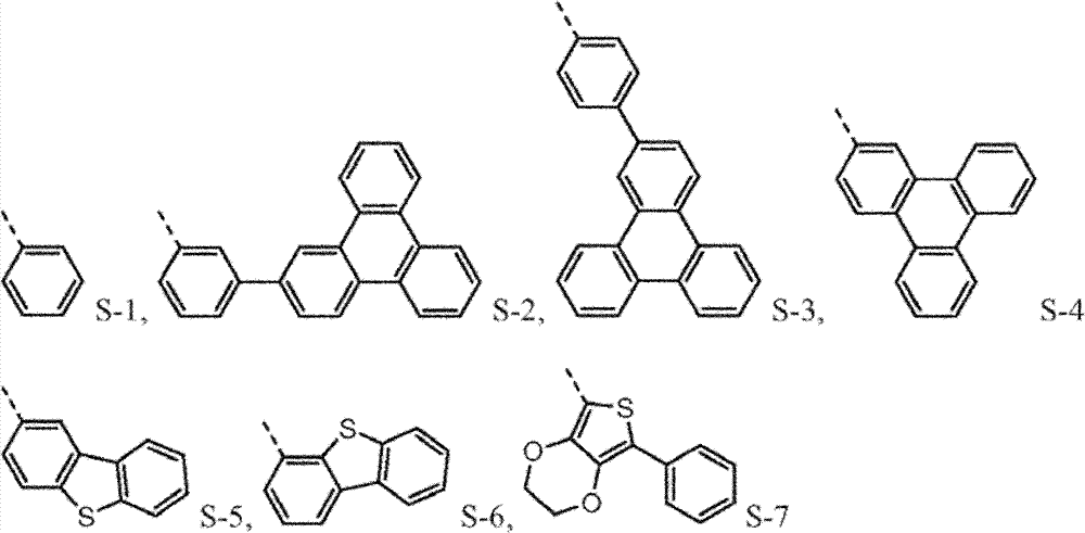
Wherein dotted line represents the tie point with the N atom of formula I.R
1, R
2, R
3and R
4be one of at least:
R
1, R
2, R
3and R
4separately can by not with R
1, R
2, R
3and R
4the substituting group condensing further replaces.Preferably, R
1, R
2, R
3and R
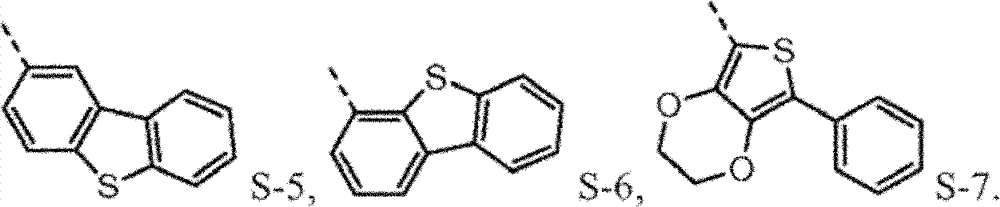
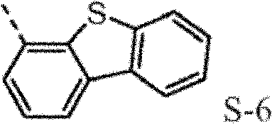
4be one of at least S-5.Preferably, R
1, R
2, R
3and R
4be one of at least S-6.Preferably, R
1, R
2, R
3and R
4be one of at least S-7.Preferably, R
1and R
2be S-6.
On the one hand, the material with chemical structural formula I providing more specifically has formula II.
On the other hand, R
1, R
2, R
3and R
4be selected from independently of one another S-1 and S-5 to S-7.
Again on the one hand, R
1, R
2, R
3and R
4be one of at least S-8 or S-9.Another aspect, R
1, R
2, R
3and R
4be selected from independently of one another S-1 and S-5 to S-9.
The specific examples that the material composition (composition of matter) with formula I is provided, it comprises the material that is selected from A-1 to A-6.Preferably, this material consists of A-1.In addition, provide the specific examples of the material composition with formula I, it comprises the material that is selected from B-1 to B-6.Preferably, this material consists of B-1.In addition, provide the specific examples of the material composition with formula I, it comprises the material that is selected from C-1 to C-6.Preferably, this material consists of C-1.In addition, provide the specific examples of the material composition with formula I, it comprises the material that is selected from D-1 to D-6.Preferably, this material consists of D-1.
The consuming product that organic luminescent device are also provided and contained such device are wherein used as hole mobile material by this novel material in this device.In device or consuming product that the selection that the material with formula I in the described material that is preferred for having formula I forms is also preferred for comprising the material with formula I.These selections comprise for substituent R
1, R
2, R
3and R
4described, formula II, and structure A-1 to A-6, B-1 to B-6, C-1 to C-6 and D-1 to D-6.
The combination of this hole mobile material and special body material is also provided.On the one hand, this main body is the compound that comprises the benzophenanthrene that contains benzo-fused thiophene.
Accompanying drawing explanation
Fig. 1 shows organic luminescent device.
Fig. 2 shows does not have the independently inversion organic luminescent device of electron transfer layer.
Fig. 3 shows the chemical formula of new compound.
Embodiment
Conventionally, OLED comprises between anode and negative electrode and at least one organic layer being connected with cathodic electricity with anode.When applying electric current, anode is to injected hole in organic layer, and negative electrode injects electronics in organic layer.Injected holes and electronics move to the electrode of oppositely charged separately.When electronics and hole are confined in same a part, form " exciton ", it is the electron-hole pair with the localization of the energy state of exciting.When exciton passes through luminescence mechanism relaxation, transmitting bright dipping.In some cases, exciton can excite on body or exciplex in localization.Also non-radiative mechanism can occur, for example thermal relaxation, is still regarded as undesirable conventionally.
Initial OLEDs is used the light emitting molecule from its singlet luminous (" fluorescence "), and for example U.S. Patent No. 4,769, and disclosed in 292, its full content is included in herein by reference.Fluorescent emission usually occurs in the time range that was less than for 10 nanoseconds.
Recently, shown the OLEDs having from the luminescent material of triplet state luminous (" phosphorescence ").See " Highly Efficient Phosphorescent Emission FromOrganic Electroluminescent Devices " (high efficiency phosphorescent transmitting of organic electroluminescence device) of the people such as Baldo, Na ture, the 395th volume, 151-154,1998; The people's such as (" Baldo-I ") and Baldo " Very high-efficiency green organiclight-emitting devices based on electrophosphorescence " (utmost point efficient green organic luminescent device based on electrophosphorescent), APPL.PHYS.LETT, the 75th volume, the 3rd phase, 4-6 (1999) (" Baldo-II "), they are all included in herein by reference.Phosphorescence is recorded in U.S. Patent No. 7,279 in more detail, 704 5-6 hurdle, and it is included in herein by reference.
Fig. 1 has shown organic luminescent device 100.These figure not necessarily draw in proportion.Device 100 can comprise substrate 110, anode 115, hole injection layer 120, hole transmission layer 125, electronic barrier layer 130, luminescent layer 135, hole blocking layer 140, electron transfer layer 145, electron injecting layer 150, protective layer 155 and negative electrode 160.Negative electrode 160 is the composite cathodes with the first conductive layer 162 and the second conductive layer 164.Device 100 can be by depositing above-mentioned layer to prepare in order.The character of the layer that these are different and function and examples of materials are more specifically recorded in US 7,279, and in 704 6-10 hurdle, it is included in herein by reference.
Can obtain the more examples of every kind in these layers.For example, the combination of flexible and transparent substrate-anode is disclosed in U.S. Patent No. 5,844, and in 363, its full content is included in herein by reference.An example of the hole transmission layer of p-type doping is the mol ratio F with 50: 1
4the m-MTDATA of TCNQ doping, is disclosed in U.S. Patent Application Publication No.2003/0230980, and its full content is included in herein by reference.The example of luminescent material and material of main part is disclosed in the people's such as Thompson U.S. Patent No. 6,303,238, and its full content is included in herein by reference.An example of the electron transfer layer of N-shaped doping is the BPhen adulterating with Li with the mol ratio of 1: 1, is disclosed in U.S. Patent Application Publication No.2003/0230980, and its full content is included in herein by reference.U.S. Patent No. 5,703,436 and 5,707,745 (its full content is included in herein by reference) disclose the example of the negative electrode that comprises composite cathode, and it has metal as the thin layer of Mg:Ag, the chlamydate electrically conducting transparent sputtering sedimentation of tool I TO layer.The theory on blocking layer and purposes are recorded in U.S. Patent No. 6,097 in more detail, 147 and U.S. Patent Application Publication No.2003/0230980 in, its full content is included in herein by reference.The example of input horizon is provided in U.S. Patent Application Publication No.2004/0174116, and its full content is included in herein by reference.Explanation about protective layer can see in U.S. Patent Application Publication No.2004/0174116, and its full content is included in herein by reference.
Fig. 2 has shown inversion OLED 200.This device comprises substrate 210, negative electrode 215, luminescent layer 220, hole transmission layer 225 and anode 230.Device 200 can be prepared by depositing in order described layer.Because most conventional OLED structure has the negative electrode being positioned on anode, and device 200 has the negative electrode 215 being positioned under anode 230, therefore device 200 can be called to " inversion " OLED.In can the corresponding layer for device 200 for the illustrated similar material of device 100.Fig. 2 provides can be how by some layer elliptical example from the structure of device 100.
Simple layered structure shown in Fig. 1 and 2 provides in the mode of limiting examples, and should be appreciated that embodiment of the present invention can be combined with a variety of other structures.Described concrete material and structure are exemplary, and can use other material and structure.Based on design, performance and cost factor, can be by by different way above-mentioned multiple layer being combined or layer is omitted obtain functional OLEDs completely.Also can comprise other layer not clearly stating.Can use the material beyond the material that clearly states.Although a lot of examples that provide are described as a lot of layers to comprise single material, should be appreciated that the combination that can use material, for example mixture of main body and doping agent or more generally mixture herein.In addition, layer can have a plurality of subgrades.Give herein and do not intend to have strict restricted with the title of various layers.For example, in device 200, hole transmission layer 225 transporting holes to injected hole in luminescent layer 220, and can be described as hole transmission layer or hole injection layer.In one embodiment, OLED can be described to have " organic layer " between negative electrode and anode.This organic layer can comprise single layer, or can comprise a plurality of layers as the different organic materials described in for Fig. 1 and 2.
Also can use the structure and material not clearly stating, for example, comprise the OLEDs (PLEDs) of polymer materials, disclosed in the U.S. Patent No. 5,247,190 such as people such as Friend, its full content is included in herein by reference.As further example, can use the OLEDs with single organic layer.OLEDs can be stacked, and described in the U.S. Patent No. 5,707,745 as people such as Forrest, its full content is included in herein by reference.OLED structure can depart from the simple laminate structure shown in Fig. 1 and 2.For example, substrate can comprise that the reflecting surface of angulation is to improve outer coupling (out-coupling), U.S. Patent No. 6 such as people such as Forrest, 091, the people's such as the platform of recording in 195 (mesa) structure and/or Bulovic U.S. Patent No. 5, the trap of recording in 834,893 (pit) structure, its full content is included in herein by reference.
Unless otherwise indicated, any layer of various embodiments can deposit by any suitable method.For organic layer, preferred method comprises thermal evaporation, ink-jet, and for example, as U.S. Patent No. 6,013, institute records in 982 and 6,087,196, and its full content is included in herein by reference; Organic vapor phase deposition (OVPD), such as recording in the U.S. Patent No. 6,337,102 as people such as Forrest, its full content is included in herein by reference; And by the deposition of organic gas phase spraying (OVJP), for example, as U.S. Patent application No.10/233, in 470 record, its full content is included in herein by reference.Other suitable deposition method comprises spin coating and other method based on solution.Method based on solution is preferably carried out in nitrogen or inert atmosphere.For other layer, preferred method comprises thermal evaporation.Preferred become pattern method comprise by mask deposit, cold welding, for example, as U.S. Patent No. 6,294, in 398 and 6,468,819 record, its full content is included in herein by reference; And as relevant with OVJD in ink-jet to some deposition method become pattern method.Also can use other method.The material that can treat deposition carries out modification so that they are compatible with concrete deposition method.For example, can in small molecules, use substituting group for example branching or alkyl and aryl non-branching and that preferably contain at least 3 carbon, to strengthen the ability that they carry out solution processing.Can use the substituting group with 20 or more carbon, 3 to 20 carbon are preferable range.The material with unsymmetric structure can have better solution processable than the material with symmetrical structure, because asymmetric material can have lower recrystallization tendency.The ability that dendrimer substituting group can carry out solution processing for improving small molecules.
The device of preparing according to embodiment of the present invention can be included in a variety of consuming product, comprises flat-panel monitor, computer monitor, TV, billboard, indoor or outdoors head light and/or signal lamp, danger warning indicating meter, all-transparent indicating meter, flexible display, laser printer, phone, mobile telephone, personal digital assistant (PDAs), notebook computer, digital camera, camcorder, view finder, miniscope, the vehicles, big area wall, arenas and stadium screen or sign.Various control mechanism can, for controlling device prepared in accordance with the present invention, comprise passive matrix and active matrix.A lot of devices are intended for in the comfortable temperature range of human body, and for example 18 ℃ to 30 ℃, more preferably room temperature (20 to 25 ℃).
Material described herein and structure can be applied in the device except OLEDs.For example, other photoelectric device can use these materials and structure as organic solar batteries and organic photoelectric detector.More generally, organic assembly for example organic transistor can use these materials and structure.
Term halogen, halogen, alkyl, cycloalkyl, thiazolinyl, alkynyl, aralkyl (arylkyl), heterocyclic group, aryl, aromatic group and heterocyclic radical are known in the art, and be defined in US7, in 279,704 31-32 hurdle, this patent is included in herein by reference.
Provide new material to form.This new material forms similar " core " comprising with naphthyl phenyl benzidine (α-NPD).In this article, the core of α-NPD has by two benzyl ring two nitrogen-atoms connected to one another, allly all in contraposition, connects.The new material composition for core with more possibility is provided, and described core comprises two nitrogen-atoms that connect by 1,2 or 3 benzyl ring, and wherein each connection can be contraposition or a position independently.At least one group being connected with the nitrogen-atoms of core comprises sulfur-containing group.Thereby, provide the new material with following structure to form:
(formula I)
Wherein n is 1,2 or 3, and the benzyl ring between nitrogen-atoms can connect on the independent contraposition of selecting or a position and is being connected with nitrogen-atoms and is connected to each other for each.R
1, R
2, R
3and R
4separately can be independently selected from following group:

Wherein dotted line represents the tie point with the N atom of formula I.R
1, R
2, R
3and R
4be one of at least:
R
1, R
2, R
3and R
4separately can by not with R
1, R
2, R
3and R
4the substituting group condensing further replaces.
Be not subject to about why needing the restriction of any theory of this novel material, it is believed that p-diaminodiphenyl (4,4 '-benzidine) core (and herein described version) is to need especially.Having a phenyl being connected on each nitrogen and the p-diaminodiphenyl of a 1-naphthyl is α-NPD, and it is widely used hole transmission layer in OLEDs.Yet α-NPD is in some device, particularly (it has more high-octane triplet state and charge carrier) in blue light and green device, can not work well.It is believed that aspect high energy charge carrier and triplet state, the naphthyl of α-NPD may be this instable reason, and disclosed sulfur-containing group (preferably dibenzothiophene (DBT)) in group A-D in this article, has in this respect higher stability.
The hole mobile material that contains dibenzothiophene group with contain other group for example the device of biphenyl, naphthalene compare and can there is higher efficiency and/or longer life-span.It is believed that be important factor for HTL aspect phosphorescence device stability at following 2: when 1) HTL should be at transporting holes, there is good hole (oxidation) stability, but also should there is good electronics (reduction) stability; 2) HTL should have than the higher triplet energy state of doping agent in its adjacent luminescent layer, to prevent that it is by the quencher of exciton transition institute.Dibenzothiophene is the conjugated compound with reversible reduction (passing through solution electrochemistry), shows that it can be stable electron carrier.In addition, dibenzothiophene self has than a lot of other organic molecules for example biphenyl, the much higher triplet energy state (414nm) of naphthalene.Stability and efficiency containing the strengthening of the HTL of dibenzothiophene can be owing to the combinations of above effect.This can cause using the device of described HTL material to have than using for example higher stability and the efficiency of device of α-NPD of conventional H TL herein.
The hole mobile material that contains 3,4-ethylidene dioxy thiophene (EDOT) group may also need, for example higher hole-conductive rate, thereby low device voltage.Poly-(3,4-ethylidene dioxy thiophene) is (PEDOT) very important conductive polymers.It has been widely used in antistatic coating with the title complex of poly-(styrene sulfonic acid) and for the hole injection layer of polymkeric substance OLEDs.Oxygen base ethane bridging between 3,4 positions of monomer makes thiophene be rich in very much electronics, therefore causes enough HOMO to raise, and forces by 2,5 open positions generation polymerizations, produces polymkeric substance linear, height conjugation.The oxidised form of this polymkeric substance is high stability under envrionment conditions.The redox property of film does not change within the long time.Hope for example includes, in triarylamine HTL (p-diaminodiphenyl) skeleton EDOT module to improve the redox property of hole injection/transport material in.The direct connection of EDOT and nitrogen-atoms will promote the HOMO of molecule, and therefore make it better with ITO interphase match.
Preferably, the sulfur-containing group of group A-D is directly connected with the nitrogen-atoms of core.It is believed that so direct connection keeps the higher triplet energy state of molecule, this expects under many circumstances.
Preferably, R
1and R
3one of at least and R
2and R
4be one of at least the group of the sulfur-containing group that comprises one of group A-D.Although it is operable having the molecule of the sulfur-containing group being connected with only nitrogen of core, it is believed that the molecule with at least one sulfur-containing group being connected with each nitrogen of core causes more stable molecule.In addition, it is believed that after there is at least one sulfur-containing group being connected with each nitrogen, add extra sulfur-containing group can not cause further improving.Although conventionally more easily use only a kind of sulfur-containing group in molecule, may use repeatedly, also can in identical molecule, use different sulfur-containing groups.
The core of α-NPD is preferred, and the part of this composition that its Chinese style I represents is more specifically:

The molecule that can be preferably as follows: R wherein
1, R
2, R
3and R
4be selected from independently of one another:
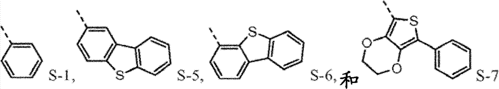
Such molecule comprises at least one sulfur-containing group in each of group A-D, and is not that any substituting group of this group is phenyl, and it should strong effect sulfur-containing group give the electronic property of this molecule.For the reason identical with phenyl, can use following substituting group:

The molecule that according to circumstances, can preferably comprise each sulfur-containing group of disclosed herein group of A-D.
Can be preferably R wherein
1, R
2, R
3and R
4be one of at least
Material form.These compounds can be called and belong to A group compound.The limiting examples that comprises this substituent concrete preferred molecule comprises:


Can be preferably R wherein
1, R
2, R
3and R
4be one of at least
Material form.These compounds can be called and belong to B group compound.The limiting examples that comprises this substituent concrete preferred molecule comprises:
Can be preferably R wherein
1and R
2be

Material form.These compounds can be called and belong to C group compound.C group compound is the subset of B group compound.The limiting examples that comprises this substituent concrete preferred molecule comprises:
Can be preferably R wherein
1, R
2, R
3and R
4be one of at least
Material form.These compounds can be called and belong to D group compound.The limiting examples that comprises this substituent concrete preferred molecule comprises:


R group for not comprising the sulfur-containing group of one of group A-D, preferably descends array structure:
The material of the formula I being preferably as follows forms: R wherein
1, R
2, R
3and R
4be selected from independently of one another:
R
1, R
2, R
3and R
4one of be at least selected from:

And do not exist R
1, R
2, R
3and R
4further replacement.
The material of the formula I being preferably as follows forms: R wherein
1, R
2, R
3and R
4be selected from independently of one another:
R
1, R
2, R
3and R
4one of be at least selected from:
And do not exist R
1, R
2, R
3and R
4further replacement.
Synthesized molecule A-1, B-1, C-1 and D-1, and provide synthetic explanation.Other molecule in A, B, C and D component and the herein version of described those molecules can be used similar chemosynthesis to be easily prepared.
Organic luminescent device is also provided.This device comprises anode, negative electrode and the organic luminous layer between anode and negative electrode.Organic luminous layer can comprise main body and phosphorescent dopants.This device also can comprise between organic luminous layer and anode and the organic cavity transmission layer that comprises hole mobile material directly contacting with organic luminous layer.Hole transmission layer can have the structure that new material disclosed herein forms, and has the structure of the novel material of the core that meets formula I.Phosphorescent dopants is organic metal iridium material preferably.
In addition, also provide consuming product, wherein these consuming product comprise organic luminescent device, and the material that this organic luminescent device comprises the structure with described formula I forms.The substituting group that the described material that is preferred for having formula I structure forms and structure choice are also preferred for comprising to be had in the device that the material of formula I structure forms or in the consuming product that comprise this device.These selections comprise for substituent R
1, R
2, R
3and R
4described, formula II, and structure A-1 to A-6, B-1 to B-6, C-1 to C-6 and D-1 to D-6.
Prepared R
1, R
2, R
3and R
4be one of at least

Organic luminescent device.Specifically, use molecule B-1 fabricate devices, and believe that other molecule with identical sulfur-containing group disclosed herein will have similar performance.This device has particularly preferred performance.
It is believed that the compound with sulfur-containing group disclosed herein is when as hole transmission layer, main body is to work especially well in the device of the compound that comprises the benzophenanthrene that contains benzo-fused thiophene therein.It is Ma that such main body is disclosed in invention people, Bin, is filed in the U.S. Patent application 61/013,391 on December 28th, 2007, and its full content is included this paper by reference in, particularly for claimed theme.Compound 2 is examples of such main body.B group material is the hole mobile material for this combinatorial optimization.
Except phosphorescent OLED s, described sulfur-bearing hole mobile material also needs for the use in fluorescence OLEDs herein.
In this article, following compounds has lower array structure:
Compound 1-is disclosed in JP 2000-299497:
It is Ma that compound 2-is disclosed in invention people, Bin, be filed in the U.S. Patent application 61/013,391 on December 28th, 2007,

Two (2-methyl-oxine) (4-phenylphenol) aluminium (BAlq) and three (oxine) aluminium (Alq
3) be known material.LG-101 and LG-201 are can be from Korea S LG Chem, the proprietary material that Inc. buys.
Experiment
A-1's is synthetic

Synthesizing of 2-bromine dibenzothiophene: dibenzothiophene (15g, 79.9mmol) is dissolved in 1.5L chloroform.In this solution, drip bromine (12.76g, 79.9mmol).By reaction mixture vigorous stirring 2 days at room temperature, then with sodium sulfite aqueous solution, process.Organic phase evaporation is obtained to white solid, based on GC-MS and HPLC result, its have 48% unreacted dibenzothiophene, 50% 2-bromine dibenzothiophene peace treaty be less than 2% 2,8-dibromo dibenzothiophene.By this mixture with ethyl acetate repeatedly recrystallization to obtain pure 2-bromine dibenzothiophene.
A-1's is synthetic: by 2-bromine dibenzothiophene (9.19mmol), diamines (1.45g, 4.18mmol), Pd (OAc)
21M tertiary butyl phosphine (0.25mL, 0.25mmol) in (30mg, 0.125mmol), toluene, t-BuONa (1.3g, 12.8mmol) and 150mL toluene add in 250mL round-bottomed flask.Reaction mixture reflux under nitrogen atmosphere is spent the night.Reaction mixture is cooling and separated with silicagel column, obtain about 2.6g (89%) product, this product is confirmed by proton N MR.
B-1's is synthetic

In 500mL round-bottomed flask, add N, N '-diphenylbenzidine (2.4g, 7mmol), 4-iodine dibenzothiophene (5.6g, 18mmol), Pd
2(dba)
3(0.2g, 0.2mmol), 2-dicyclohexyl phosphorus-2 ', 4 ', 6 '-tri isopropyl biphenyl (XPhos, 0.4g, 0.8mmol), sodium tert-butoxide (2.9g, 30mmol) and 150mL toluene.Reaction is heated to reflux and under nitrogen atmosphere, stir 24 hours.After cooling, mixture is passed through to silicagel column purifying.Output is 2g.
C-1's is synthetic

N-(dibenzo [b, d] thiophene-4-yl)-N-(4-p-methoxy-phenyl) dibenzo [b, d] thiophene-4-amine: by acid chloride (0.07g, 1.0M tri-(tertiary butyl) phosphine solution (0.67mL, 0.67mmol) 0.33mmol) and in toluene adds in the three-necked flask under nitrogen atmosphere.Then add 150mL toluene.This solution is stirred under nitrogen atmosphere until color disappears.In this solution, add successively 4-iodine dibenzothiophene (7.4g, 24mmol), sodium tert-butoxide (3.3g, 33mmol) and 4-anisidine (1.4g, 11mmol).Then by this mixture reflux 4 hours.After being cooled to room temperature, mixture is filtered by silica gel short column (plug).By product, by column chromatography purifying, in use hexane, 30% methylene dichloride is as eluent.After purifying, obtain the target product of 4.6g.(productive rate 85%)
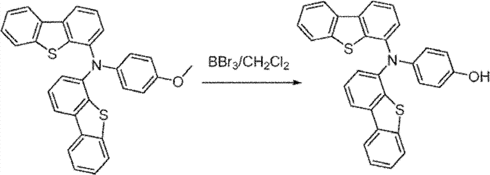
4-(two (dibenzo [b, d] thiophene-4-yl) amino) phenol synthetic: by N-(dibenzo [b, d] thiophene-4-yl)-N-(4-p-methoxy-phenyl) dibenzo [b, d] thiophene-4-amine (4.6g, 9.4mmo l) is dissolved in 100mL anhydrous methylene chloride.This solution is bathed cooling by dry ice/isopropanol.To the solution that adds in this solution boron tribromide in hexane (1.0M solution, 16mL).Make reaction be warming up to room temperature, continue 6 hours.To react water all standing.Product is purified by column chromatography, use methylene dichloride as eluent.Obtain 4g target product.(productive rate 90%)

Synthesizing of 4-(two (dibenzo [b, d] thiophene-4-yl) amino) phenyl trifluoromethanesulfonate methane sulfonate:
4-(two (dibenzo [b, d] thiophene-4-yl) amino) phenol (4.0g, 8.4mmo l) is dissolved in 60mL anhydrous methylene chloride.This solution is cooling with ice-water bath.In this solution, add pyridine (1.7mL, 21mmo l), then add trifluoromethanesulfanhydride anhydride (1.7mL, 10.1mmol).To react and stir 20 minutes, then water all standing.Organic layer is separated.By solvent vapourisation under reduced pressure.Resistates is purified by column chromatography, use the methylene dichloride of 1: 3 and hexane as eluent.Obtain the target product of 4.15g.(productive rate 82%)
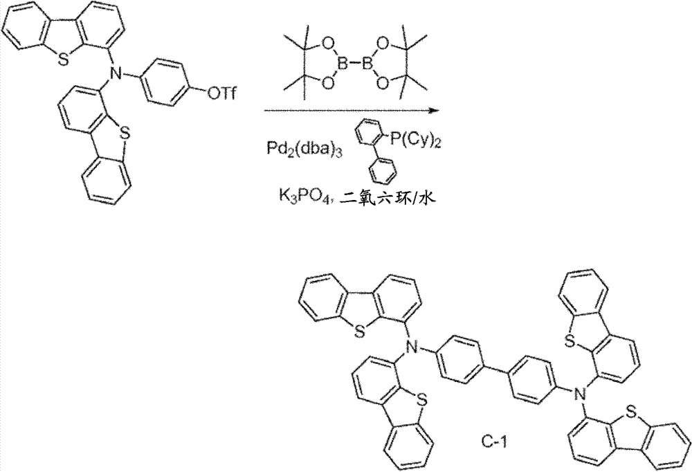
C-1, N
4, N
4, N
4', N
4'-tetra-(dibenzo [b, d] thiophene-4-yl) biphenyl-4, synthesizing of 4 '-diamines: by 4-(two (dibenzo [b, d] thiophene-4-yl) amino) phenyl trifluoromethanesulfonate methane sulfonate (4.0g, 6.6mmol), two tetramethyl ethylene ketones close two boron (0.84g, 3.3mmol), biphenyl-2-base dicyclohexylphosphontetrafluoroborate (0.09g, 0.26mmol), potassiumphosphate (3.5g, 16.5mmol) add in three-necked bottle.Then add 100mL dioxane and 5mL water.Mixture is used to nitrogen purging 30 minutes.Add Pd
2(dba)
3(0.06g, 0.07mmol).Through reaction mixture, at 60 ℃, heat 4 hours.Reaction mixture is filtered by sal epsom bed.Then solvent is evaporated.Resistates is dissolved in methylene dichloride, then uses isopropanol precipitating.Solid by filtration is collected.Product is further purified by post, uses the methylene dichloride of 1: 2 to 1: 1 and hexane as eluent.Obtain 2g target product.
D-1's is synthetic
2,5-bis-is bromo-3,4-ethylidene dioxy thiophene synthetic: 3,4-ethylidene dioxy thiophene (EDOT) (5g, 35mmo l) is dissolved in the mixture of 70mL THF and 70mL acetic acid.NBS (13.2g, 74mmol) is slowly added in this solution.Reaction is at room temperature stirred 2 hours, then add 350mL water.Precipitation is collected and washed with water by filtration.By the silver gray solid of collection dried overnight in applying the moisture eliminator of vacuum, obtain 10.3g2,5-bis-is bromo-3,4-ethylidene dioxy thiophene (33mmol, productive rate 94.6%).

2-is bromo-3,4-ethylidene dioxy thiophene synthetic: the bromo-EDOT of 2,5-bis-(10.3g, 33mmol) is dissolved in the anhydrous THF of 200mL and by acetone/the dry ice bath and is cooled to-78 ℃.Then in this solution, drip 22.1mL n-BuLi (1.6M, in hexane).After being warming up to room temperature, will reacting by 170mL HCl (1M) all standing and with methylene dichloride (200mL * 2) and extract.By the organic layer MgSO of merging
4dry and concentrate by Rotary Evaporators, obtain 10.5 grams of brown liquids, this liquid be not further purified and is moistly being directly used in next step to constant weight in the situation that.
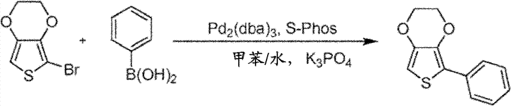
2-phenyl-3,4-ethylidene dioxy thiophene synthetic: the mixture of the preparation bromo-EDOT of 2-(10.5g, 47mmol), phenyl-boron dihydroxide (8.1g, 66mmol), Tripotassium phosphate (30g, 142.5mmol), 300mL toluene and 30mL water.By the direct bubbling 15 minutes in this mixture of nitrogen.Then add three (dibenzalacetone) two palladiums (435mg, 0.48mmol) and S-Phos (788mg, 1.92mmol).By nitrogen bubbling 15 minutes again in mixture.Reaction mixture is flow through to night next time at nitrogen atmosphere.Second day is cooled to room temperature by reaction mixture.By organic layer separation and by waterbearing stratum dichloromethane extraction.By the organic layer dried over mgso merging, filter and under reduced pressure concentrate.By the black oil obtaining by bulb (Kuge lrohr) 160 ℃ of distillations to remove black.Then by bulb, the distillation of 100 ℃, successfully remove impurity.In the situation that not being further purified, by 6 grams of (27.5mmol, overall yields of rear two steps: 83%) light yellow oil is for next step retaining in original flask.
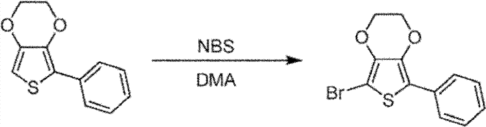
The bromo-5-of 2-phenyl-3,4-ethylidene dioxy thiophene synthetic: 2-phenyl-EDOT (6g, 28mmol) is dissolved in DMA and by ice bath and is cooled to 0 ℃, and use nitrogen bubble.NBS (5.4g, 30.2mmol) is dissolved in 35mL DMA, and under nitrogen atmosphere, is added drop-wise in 2-phenyl-EDOT solution.After adding all NBS, make reaction be warming up to room temperature and stir 20 minutes.Then mixture is poured in frozen water, used dichloromethane extraction.By the organic layer dried over mgso merging, filter and concentrate by Rotary Evaporators and bulb.By red solid recrystallization from hot methanol, obtain 5.7 grams of gray solid (19mmol, productive rate 70%).

D-1's is synthetic: the mixture of the preparation bromo-5-phenyl-EDOT of 2-(2g, 6.7mmol), diphenylbenzidine (0.57g, 1.68mmol), t-BuONa (0.48g, 5.04mmol) and dimethylbenzene (80mL).By the direct bubbling 15 minutes in this mixture of nitrogen.Then add three (dibenzalacetone) two palladiums (23mg, 1.5% equivalent) and S-Phos (41mg, 6% equivalent).Reaction mixture is flow through to night next time at nitrogen atmosphere.Second day is cooled to room temperature by reaction mixture, then by celite short column, is filtered and is washed out with methylene dichloride.Filtrate is concentrated and is used column purification (first use in hexane 15% EtOAc, then wash as solvent with 30% EtOAc in hexane and 10% methylene dichloride).By hot methylene dichloride and recrystallizing methanol for the yellow solid obtaining, obtain 0.7g (0.5mmol, productive rate 30%) yellow solid.
Device
Use standard technique fabricate devices.These devices have and similar structure shown in Fig. 1, but comprise concrete layer and the material described in table.
Table 1: the structure vs. comparative example with the green glow PHOLEDs of new HTL material and new main body/HTL combination.

Table 2: the performance vs. comparative example with the green glow PHOLEDs of new HTL material and new main body/HTL combination.
2 groups of experiments have been shown in table 1 and 2.Shown the green glow PHOLED device performance outstanding with respect to the device with NPD HTL with new HTL material B-1.Also shown that it is desirable that the HTL material that is similar to B-1 is used in combination with the main body that is similar to compound 2.
Group 1: embodiment 1 and 2
Difference between embodiment 1 (contrast) and embodiment 2 is that embodiment 1 has α-NPDHTL, and embodiment 2 has the HTL of compd B-1.HTL B-1 with compound 2 combination results as main body compare better result with using the similar device of α-NPD HTL.Embodiment 2 has shown in better properties aspect efficiency and life-span.In addition, the result of embodiment 2 is particularly preferred for green light device on the whole, and it is desirable showing the HTL with the compound that is similar to B-1 to be used in combination with the main body that is similar to compound 2.
Group 2: embodiment 3 and 4
Group 2 has been carried out and has been organized similarly contrast in 1, and difference is to replace LG-201 with the ETL of Alq.From organizing, 2, can draw and organize conclusion identical in 1.
Described can use with multiple other combination of materials of existing in device for the material of the certain layer in organic luminescent device herein.For example, light-emitting dopant disclosed herein can be used in combination with multiple main body, transport layer, blocking layer, input horizon, electrode and other layer that can exist.Described or following material is the limiting examples of the material that can use with compound combination disclosed herein, and those skilled in the art easily By consulting literatures determine other material that can be used in combination.
Except material disclosed herein, and/or combined with material disclosed herein, can in OLED, use a lot of hole-injecting materials, hole mobile material, material of main part, dopant material, exciton/hole barrier layer material, electric transmission and electron injection material.The limiting examples of the material can be in OLED using with combination of materials disclosed herein is listed in the table below in 3.Table 3 has been enumerated the limiting examples of nonrestrictive material classification, each compounds and is disclosed the document of these materials.
Table 3


Should be appreciated that described multiple embodiments, as just example, is not used in and limits the scope of the invention herein.For example, in the situation that not departing from spirit of the present invention, described a lot of materials and structure can substitute by other material and structure herein.Therefore, claimed the present invention can comprise the version of apparent specific embodiment and preferred embodiment to those skilled in the art.Should be appreciated that the multiple theory about why the present invention can set up is nonrestrictive.
Claims (22)


Applications Claiming Priority (3)
| Application Number | Priority Date | Filing Date | Title |
|---|---|---|---|
| US7707308P | 2008-06-30 | 2008-06-30 | |
| US61/077,073 | 2008-06-30 | ||
| PCT/US2009/049186 WO2010002848A1 (en) | 2008-06-30 | 2009-06-30 | Hole transport materials having a sulfur-containing group |
Publications (2)
| Publication Number | Publication Date |
|---|---|
| CN102131891A CN102131891A (en) | 2011-07-20 |
| CN102131891B true CN102131891B (en) | 2014-01-29 |
Family
ID=40933691
Family Applications (1)
| Application Number | Title | Priority Date | Filing Date |
|---|---|---|---|
| CN200980132488.0A Active CN102131891B (en) | 2008-06-30 | 2009-06-30 | Hole transport materials having a sulfur-containing group |
Country Status (6)
| Country | Link |
|---|---|
| US (1) | US8652653B2 (en) |
| EP (2) | EP2321376B1 (en) |
| JP (2) | JP5536054B2 (en) |
| KR (3) | KR20160140980A (en) |
| CN (1) | CN102131891B (en) |
| WO (1) | WO2010002848A1 (en) |
Families Citing this family (137)
| Publication number | Priority date | Publication date | Assignee | Title |
|---|---|---|---|---|
| KR101600624B1 (en) | 2006-02-10 | 2016-03-21 | 유니버셜 디스플레이 코포레이션 | METAL COMPLEXES OF CYCLOMETALLATED IMIDAZO[1,2-f]PHENANTHRIDINE AND DIIMIDAZO[1,2-A:1',2'-C]QUINAZOLINE LIGANDS AND ISOELECTRONIC AND BENZANNULATED ANALOGS THEREOF |
| CN102131891B (en) * | 2008-06-30 | 2014-01-29 | 通用显示公司 | Hole transport materials having a sulfur-containing group |
| US8288187B2 (en) | 2010-01-20 | 2012-10-16 | Universal Display Corporation | Electroluminescent devices for lighting applications |
| US20120319091A1 (en) * | 2010-01-21 | 2012-12-20 | Idemitsu Kosan Co., Ltd. | Aromatic amine derivative, and organic electroluminescent element comprising same |
| JP4751954B1 (en) * | 2010-07-09 | 2011-08-17 | 富士フイルム株式会社 | Organic electroluminescence device |
| WO2012029253A1 (en) * | 2010-08-31 | 2012-03-08 | 出光興産株式会社 | Nitrogen-containing aromatic heterocyclic derivative and organic electroluminescence device using same |
| US8748012B2 (en) | 2011-05-25 | 2014-06-10 | Universal Display Corporation | Host materials for OLED |
| JP6081210B2 (en) * | 2012-02-10 | 2017-02-15 | ケミプロ化成株式会社 | Compound exhibiting exciplex emission in a single molecule |
| US9386657B2 (en) | 2012-03-15 | 2016-07-05 | Universal Display Corporation | Organic Electroluminescent materials and devices |
| KR101907671B1 (en) * | 2012-04-17 | 2018-10-16 | 덕산네오룩스 주식회사 | Compound for organic electronic element, organic electronic element using the same, and a electronic device thereof |
| DE102012104118B4 (en) | 2012-05-10 | 2021-12-02 | Heliatek Gmbh | Hole transport materials for optoelectronic components |
| US9540329B2 (en) | 2012-07-19 | 2017-01-10 | Universal Display Corporation | Organic electroluminescent materials and devices |
| US9252363B2 (en) | 2012-10-04 | 2016-02-02 | Universal Display Corporation | Aryloxyalkylcarboxylate solvent compositions for inkjet printing of organic layers |
| US9196860B2 (en) | 2012-12-04 | 2015-11-24 | Universal Display Corporation | Compounds for triplet-triplet annihilation upconversion |
| US8716484B1 (en) | 2012-12-05 | 2014-05-06 | Universal Display Corporation | Hole transporting materials with twisted aryl groups |
| US9653691B2 (en) | 2012-12-12 | 2017-05-16 | Universal Display Corporation | Phosphorescence-sensitizing fluorescence material system |
| US10400163B2 (en) | 2013-02-08 | 2019-09-03 | Universal Display Corporation | Organic electroluminescent materials and devices |
| JP2014187130A (en) * | 2013-03-22 | 2014-10-02 | Nippon Hoso Kyokai <Nhk> | Organic electroluminescent element, display device and illuminating device, evaluation method of hole transport material |
| GB201306365D0 (en) | 2013-04-09 | 2013-05-22 | Kathirgamanathan Poopathy | Heterocyclic compounds and their use in electro-optical or opto-electronic devices |
| GB2543732A (en) * | 2015-07-20 | 2017-05-03 | Power Oleds Ltd | Heterocyclic compounds and their use in electro-optical or opto-electronic devices |
| KR102081248B1 (en) * | 2013-06-05 | 2020-02-26 | 삼성디스플레이 주식회사 | Organic light emitting diode display |
| TW201512373A (en) * | 2013-08-30 | 2015-04-01 | Kanto Kagaku | Compound and organic electroluminescence element |
| JP6481165B2 (en) * | 2013-08-30 | 2019-03-13 | 日本放送協会 | Compound and organic electroluminescence device |
| JP6348380B2 (en) * | 2013-08-30 | 2018-06-27 | 日本放送協会 | Hole transport material |
| US9876173B2 (en) | 2013-12-09 | 2018-01-23 | Universal Display Corporation | Organic electroluminescent materials and devices |
| WO2015091716A1 (en) | 2013-12-20 | 2015-06-25 | Basf Se | Highly efficient oled devices with very short decay times |
| JP6452063B2 (en) * | 2014-02-25 | 2019-01-16 | 日本放送協会 | Hole transport material |
| US9450198B2 (en) | 2014-04-15 | 2016-09-20 | Universal Display Corporation | Organic electroluminescent materials and devices |
| EP3174885B1 (en) | 2014-07-28 | 2019-10-02 | Idemitsu Kosan Co., Ltd. | 2,9-functionalized benzimidazolo[1,2-a]benzimidazoles as hosts for organic light emitting diodes (oleds) |
| EP2982676B1 (en) | 2014-08-07 | 2018-04-11 | Idemitsu Kosan Co., Ltd. | Benzimidazo[2,1-B]benzoxazoles for electronic applications |
| EP3186264B1 (en) | 2014-08-08 | 2018-11-28 | UDC Ireland Limited | Electroluminescent imidazo-quinoxaline carbene metal complexes |
| EP2993215B1 (en) | 2014-09-04 | 2019-06-19 | Idemitsu Kosan Co., Ltd. | Azabenzimidazo[2,1-a]benzimidazoles for electronic applications |
| EP3015469B1 (en) | 2014-10-30 | 2018-12-19 | Idemitsu Kosan Co., Ltd. | 5-(benzimidazol-2-yl)benzimidazo[1,2-a]benzimidazoles for electronic applications |
| JP6506534B2 (en) * | 2014-11-07 | 2019-04-24 | 三星ディスプレイ株式會社Samsung Display Co.,Ltd. | Material for organic electroluminescent device and organic electroluminescent device using the same |
| WO2016079667A1 (en) | 2014-11-17 | 2016-05-26 | Idemitsu Kosan Co., Ltd. | Indole derivatives for electronic applications |
| US10424746B2 (en) | 2014-11-18 | 2019-09-24 | Udc Ireland Limited | Pt- or Pd-carbene complexes for use in organic light emitting diodes |
| EP3034506A1 (en) | 2014-12-15 | 2016-06-22 | Idemitsu Kosan Co., Ltd | 4-functionalized carbazole derivatives for electronic applications |
| EP3034507A1 (en) | 2014-12-15 | 2016-06-22 | Idemitsu Kosan Co., Ltd | 1-functionalized dibenzofurans and dibenzothiophenes for organic light emitting diodes (OLEDs) |
| EP3054498B1 (en) | 2015-02-06 | 2017-09-20 | Idemitsu Kosan Co., Ltd. | Bisimidazodiazocines |
| EP3053918B1 (en) | 2015-02-06 | 2018-04-11 | Idemitsu Kosan Co., Ltd. | 2-carbazole substituted benzimidazoles for electronic applications |
| US9929361B2 (en) | 2015-02-16 | 2018-03-27 | Universal Display Corporation | Organic electroluminescent materials and devices |
| EP3061759B1 (en) | 2015-02-24 | 2019-12-25 | Idemitsu Kosan Co., Ltd | Nitrile substituted dibenzofurans |
| US11056657B2 (en) | 2015-02-27 | 2021-07-06 | University Display Corporation | Organic electroluminescent materials and devices |
| EP3070144B1 (en) | 2015-03-17 | 2018-02-28 | Idemitsu Kosan Co., Ltd. | Seven-membered ring compounds |
| EP3072943B1 (en) | 2015-03-26 | 2018-05-02 | Idemitsu Kosan Co., Ltd. | Dibenzofuran/carbazole-substituted benzonitriles |
| EP3075737B1 (en) | 2015-03-31 | 2019-12-04 | Idemitsu Kosan Co., Ltd | Benzimidazolo[1,2-a]benzimidazole carrying aryl- or heteroarylnitril groups for organic light emitting diodes |
| US9859510B2 (en) | 2015-05-15 | 2018-01-02 | Universal Display Corporation | Organic electroluminescent materials and devices |
| US10418568B2 (en) | 2015-06-01 | 2019-09-17 | Universal Display Corporation | Organic electroluminescent materials and devices |
| EP4060757A1 (en) | 2015-06-03 | 2022-09-21 | UDC Ireland Limited | Highly efficient oled devices with very short decay times |
| US11127905B2 (en) | 2015-07-29 | 2021-09-21 | Universal Display Corporation | Organic electroluminescent materials and devices |
| US10672996B2 (en) | 2015-09-03 | 2020-06-02 | Universal Display Corporation | Organic electroluminescent materials and devices |
| EP3150606B1 (en) | 2015-10-01 | 2019-08-14 | Idemitsu Kosan Co., Ltd. | Benzimidazolo[1,2-a]benzimidazoles carrying benzofurane or benzothiophene groups for organic light emitting diodes |
| WO2017056055A1 (en) | 2015-10-01 | 2017-04-06 | Idemitsu Kosan Co., Ltd. | Benzimidazolo[1,2-a]benzimidazole carrying triazine groups for organic light emitting diodes |
| WO2017056053A1 (en) | 2015-10-01 | 2017-04-06 | Idemitsu Kosan Co., Ltd. | Benzimidazolo[1,2-a]benzimidazole carrying benzimidazolo[1,2-a]benzimidazolyl groups, carbazolyl groups, benzofurane groups or benzothiophene groups for organic light emitting diodes |
| EP3150604B1 (en) | 2015-10-01 | 2021-07-14 | Idemitsu Kosan Co., Ltd. | Benzimidazolo[1,2-a]benzimidazole carrying benzimidazolo[1,2-a]benzimidazolylyl groups, carbazolyl groups, benzofurane groups or benzothiophene groups for organic light emitting diodes |
| KR20180079328A (en) | 2015-11-04 | 2018-07-10 | 이데미쓰 고산 가부시키가이샤 | Benzimidazole condensed heteroaryl |
| WO2017093958A1 (en) | 2015-12-04 | 2017-06-08 | Idemitsu Kosan Co., Ltd. | Benzimidazolo[1,2-a]benzimidazole derivatives for organic light emitting diodes |
| KR102684614B1 (en) | 2015-12-21 | 2024-07-15 | 유디씨 아일랜드 리미티드 | Transition metal complexes with tripodal ligands and the use thereof in oleds |
| EP3394062B1 (en) | 2015-12-21 | 2019-10-02 | Idemitsu Kosan Co., Ltd | Hetero-condensed phenylquinazolines and their use in electronic devices |
| US20170229663A1 (en) | 2016-02-09 | 2017-08-10 | Universal Display Corporation | Organic electroluminescent materials and devices |
| US10236456B2 (en) | 2016-04-11 | 2019-03-19 | Universal Display Corporation | Organic electroluminescent materials and devices |
| WO2017178864A1 (en) | 2016-04-12 | 2017-10-19 | Idemitsu Kosan Co., Ltd. | Seven-membered ring compounds |
| US9985579B2 (en) | 2016-04-12 | 2018-05-29 | Preformed Line Products Co. | Mounting assembly for mounting a solar panel |
| KR102018682B1 (en) * | 2016-05-26 | 2019-09-04 | 덕산네오룩스 주식회사 | Compound for organic electronic element, organic electronic element using the same, and an electronic device thereof |
| US10672997B2 (en) | 2016-06-20 | 2020-06-02 | Universal Display Corporation | Organic electroluminescent materials and devices |
| US10862054B2 (en) | 2016-06-20 | 2020-12-08 | Universal Display Corporation | Organic electroluminescent materials and devices |
| US11482683B2 (en) | 2016-06-20 | 2022-10-25 | Universal Display Corporation | Organic electroluminescent materials and devices |
| US10608186B2 (en) | 2016-09-14 | 2020-03-31 | Universal Display Corporation | Organic electroluminescent materials and devices |
| US10680187B2 (en) | 2016-09-23 | 2020-06-09 | Universal Display Corporation | Organic electroluminescent materials and devices |
| US11196010B2 (en) | 2016-10-03 | 2021-12-07 | Universal Display Corporation | Organic electroluminescent materials and devices |
| US11011709B2 (en) | 2016-10-07 | 2021-05-18 | Universal Display Corporation | Organic electroluminescent materials and devices |
| US12317745B2 (en) | 2016-11-09 | 2025-05-27 | Universal Display Corporation | Organic electroluminescent materials and devices |
| US10680188B2 (en) | 2016-11-11 | 2020-06-09 | Universal Display Corporation | Organic electroluminescent materials and devices |
| US11780865B2 (en) | 2017-01-09 | 2023-10-10 | Universal Display Corporation | Organic electroluminescent materials and devices |
| US10844085B2 (en) | 2017-03-29 | 2020-11-24 | Universal Display Corporation | Organic electroluminescent materials and devices |
| US10944060B2 (en) | 2017-05-11 | 2021-03-09 | Universal Display Corporation | Organic electroluminescent materials and devices |
| EP3418285B1 (en) | 2017-06-20 | 2020-05-06 | Idemitsu Kosan Co., Ltd. | Composition comprising a substituted ir complex and a phenylquinazoline bridged with a heteroatom |
| US12098157B2 (en) | 2017-06-23 | 2024-09-24 | Universal Display Corporation | Organic electroluminescent materials and devices |
| US11228010B2 (en) | 2017-07-26 | 2022-01-18 | Universal Display Corporation | Organic electroluminescent materials and devices |
| US11744142B2 (en) | 2017-08-10 | 2023-08-29 | Universal Display Corporation | Organic electroluminescent materials and devices |
| EP3466954A1 (en) | 2017-10-04 | 2019-04-10 | Idemitsu Kosan Co., Ltd. | Fused phenylquinazolines bridged with a heteroatom |
| CN109836435B (en) * | 2017-11-27 | 2021-04-13 | 北京夏禾科技有限公司 | Triarylamine compounds containing thiophene |
| US12180230B2 (en) | 2017-11-28 | 2024-12-31 | University Of Southern California | Carbene compounds and organic electroluminescent devices |
| EP3492480B1 (en) | 2017-11-29 | 2021-10-20 | Universal Display Corporation | Organic electroluminescent materials and devices |
| US11937503B2 (en) | 2017-11-30 | 2024-03-19 | Universal Display Corporation | Organic electroluminescent materials and devices |
| US11542289B2 (en) | 2018-01-26 | 2023-01-03 | Universal Display Corporation | Organic electroluminescent materials and devices |
| US11165028B2 (en) | 2018-03-12 | 2021-11-02 | Universal Display Corporation | Organic electroluminescent materials and devices |
| US12453279B2 (en) | 2018-08-22 | 2025-10-21 | Universal Display Corporation | Organic electroluminescent materials and devices |
| US11737349B2 (en) | 2018-12-12 | 2023-08-22 | Universal Display Corporation | Organic electroluminescent materials and devices |
| US11780829B2 (en) | 2019-01-30 | 2023-10-10 | The University Of Southern California | Organic electroluminescent materials and devices |
| US12477890B2 (en) | 2019-02-01 | 2025-11-18 | Universal Display Corporation | Organic electroluminescent materials and devices |
| JP2020158491A (en) | 2019-03-26 | 2020-10-01 | ユニバーサル ディスプレイ コーポレイション | Organic electroluminescent materials and devices |
| CN109994640B (en) * | 2019-04-09 | 2021-06-15 | 江苏三月科技股份有限公司 | Organic electroluminescent device containing multi-channel carrier transmission material |
| US12281128B2 (en) | 2019-07-30 | 2025-04-22 | Universal Display Corporation | Organic electroluminescent materials and devices |
| US12139501B2 (en) | 2019-08-16 | 2024-11-12 | Universal Display Corporation | Organic electroluminescent materials and devices |
| US20210135130A1 (en) | 2019-11-04 | 2021-05-06 | Universal Display Corporation | Organic electroluminescent materials and devices |
| KR102853329B1 (en) | 2019-12-11 | 2025-09-01 | 삼성디스플레이 주식회사 | Organic light emitting device and apparatus including the same |
| US12538698B2 (en) | 2020-01-06 | 2026-01-27 | Universal Display Corporation | Organic electroluminescent materials and devices |
| US12426495B2 (en) | 2020-01-28 | 2025-09-23 | Universal Display Corporation | Organic electroluminescent materials and devices |
| EP3937268B1 (en) | 2020-07-10 | 2025-05-07 | Universal Display Corporation | Plasmonic oleds and vertical dipole emitters |
| US12187748B2 (en) | 2020-11-02 | 2025-01-07 | Universal Display Corporation | Organic electroluminescent materials and devices |
| US20220158096A1 (en) | 2020-11-16 | 2022-05-19 | Universal Display Corporation | Organic electroluminescent materials and devices |
| US20220165967A1 (en) | 2020-11-24 | 2022-05-26 | Universal Display Corporation | Organic electroluminescent materials and devices |
| US12325717B2 (en) | 2020-11-24 | 2025-06-10 | Universal Display Corporation | Organic electroluminescent materials and devices |
| US20220271241A1 (en) | 2021-02-03 | 2022-08-25 | Universal Display Corporation | Organic electroluminescent materials and devices |
| CN114874231A (en) * | 2021-02-05 | 2022-08-09 | 上海和辉光电股份有限公司 | Organic electroluminescent compound and application thereof |
| EP4060758A3 (en) | 2021-02-26 | 2023-03-29 | Universal Display Corporation | Organic electroluminescent materials and devices |
| EP4059915B1 (en) | 2021-02-26 | 2025-12-24 | Universal Display Corporation | Organic electroluminescent materials and devices |
| US20220298192A1 (en) | 2021-03-05 | 2022-09-22 | Universal Display Corporation | Organic electroluminescent materials and devices |
| US12428599B2 (en) | 2021-03-09 | 2025-09-30 | Universal Display Corporation | Organic electroluminescent materials and devices |
| US20220298190A1 (en) | 2021-03-12 | 2022-09-22 | Universal Display Corporation | Organic electroluminescent materials and devices |
| US12421262B2 (en) | 2021-03-15 | 2025-09-23 | Universal Display Corporation | Organic electroluminescent materials and devices |
| US20220340607A1 (en) | 2021-04-05 | 2022-10-27 | Universal Display Corporation | Organic electroluminescent materials and devices |
| US12480042B2 (en) | 2021-04-09 | 2025-11-25 | Universal Display Corporation | Organic electroluminescent materials and devices |
| EP4075531A1 (en) | 2021-04-13 | 2022-10-19 | Universal Display Corporation | Plasmonic oleds and vertical dipole emitters |
| US20220352478A1 (en) | 2021-04-14 | 2022-11-03 | Universal Display Corporation | Organic eletroluminescent materials and devices |
| US20230006149A1 (en) | 2021-04-23 | 2023-01-05 | Universal Display Corporation | Organic electroluminescent materials and devices |
| US20220407020A1 (en) | 2021-04-23 | 2022-12-22 | Universal Display Corporation | Organic electroluminescent materials and devices |
| US20230133787A1 (en) | 2021-06-08 | 2023-05-04 | University Of Southern California | Molecular Alignment of Homoleptic Iridium Phosphors |
| EP4151699A1 (en) | 2021-09-17 | 2023-03-22 | Universal Display Corporation | Organic electroluminescent materials and devices |
| US12473318B2 (en) | 2021-10-08 | 2025-11-18 | Universal Display Corporation | Organic electroluminescent materials and devices |
| US12509628B2 (en) | 2021-12-16 | 2025-12-30 | Universal Display Corporation | Organic electroluminescent materials and devices |
| EP4231804A3 (en) | 2022-02-16 | 2023-09-20 | Universal Display Corporation | Organic electroluminescent materials and devices |
| US20230292592A1 (en) | 2022-03-09 | 2023-09-14 | Universal Display Corporation | Organic electroluminescent materials and devices |
| US20230337516A1 (en) | 2022-04-18 | 2023-10-19 | Universal Display Corporation | Organic electroluminescent materials and devices |
| US20230389421A1 (en) | 2022-05-24 | 2023-11-30 | Universal Display Corporation | Organic electroluminescent materials and devices |
| EP4293001A1 (en) | 2022-06-08 | 2023-12-20 | Universal Display Corporation | Organic electroluminescent materials and devices |
| US20240016051A1 (en) | 2022-06-28 | 2024-01-11 | Universal Display Corporation | Organic electroluminescent materials and devices |
| US20240107880A1 (en) | 2022-08-17 | 2024-03-28 | Universal Display Corporation | Organic electroluminescent materials and devices |
| US20240188319A1 (en) | 2022-10-27 | 2024-06-06 | Universal Display Corporation | Organic electroluminescent materials and devices |
| US20240188316A1 (en) | 2022-10-27 | 2024-06-06 | Universal Display Corporation | Organic electroluminescent materials and devices |
| US20240180025A1 (en) | 2022-10-27 | 2024-05-30 | Universal Display Corporation | Organic electroluminescent materials and devices |
| US20240196730A1 (en) | 2022-10-27 | 2024-06-13 | Universal Display Corporation | Organic electroluminescent materials and devices |
| US20240188419A1 (en) | 2022-10-27 | 2024-06-06 | Universal Display Corporation | Organic electroluminescent materials and devices |
| US20240247017A1 (en) | 2022-12-14 | 2024-07-25 | Universal Display Corporation | Organic electroluminescent materials and devices |
| US20250204239A1 (en) | 2023-12-15 | 2025-06-19 | Universal Display Corporation | Organic electroluminescent materials and devices |
| US20250204238A1 (en) | 2023-12-15 | 2025-06-19 | Universal Display Corporation | Organic electroluminscent materials and devices |
Citations (1)
| Publication number | Priority date | Publication date | Assignee | Title |
|---|---|---|---|---|
| WO2003064373A1 (en) * | 2002-01-28 | 2003-08-07 | Sensient Imaging Technologies Gmbh | Triarylamine derivatives and the use thereof in organic electroluminescent and electrophotographic devices |
Family Cites Families (33)
| Publication number | Priority date | Publication date | Assignee | Title |
|---|---|---|---|---|
| US1339107A (en) | 1918-08-28 | 1920-05-04 | Elmer C Dittmar | Apparatus for coating and finishing flooring |
| US4769292A (en) | 1987-03-02 | 1988-09-06 | Eastman Kodak Company | Electroluminescent device with modified thin film luminescent zone |
| GB8909011D0 (en) | 1989-04-20 | 1989-06-07 | Friend Richard H | Electroluminescent devices |
| US5707745A (en) * | 1994-12-13 | 1998-01-13 | The Trustees Of Princeton University | Multicolor organic light emitting devices |
| US5703436A (en) | 1994-12-13 | 1997-12-30 | The Trustees Of Princeton University | Transparent contacts for organic devices |
| US5844363A (en) | 1997-01-23 | 1998-12-01 | The Trustees Of Princeton Univ. | Vacuum deposited, non-polymeric flexible organic light emitting devices |
| US5834893A (en) * | 1996-12-23 | 1998-11-10 | The Trustees Of Princeton University | High efficiency organic light emitting devices with light directing structures |
| US6013982A (en) * | 1996-12-23 | 2000-01-11 | The Trustees Of Princeton University | Multicolor display devices |
| US6091195A (en) | 1997-02-03 | 2000-07-18 | The Trustees Of Princeton University | Displays having mesa pixel configuration |
| US6303238B1 (en) | 1997-12-01 | 2001-10-16 | The Trustees Of Princeton University | OLEDs doped with phosphorescent compounds |
| US6337102B1 (en) | 1997-11-17 | 2002-01-08 | The Trustees Of Princeton University | Low pressure vapor phase deposition of organic thin films |
| US6087196A (en) * | 1998-01-30 | 2000-07-11 | The Trustees Of Princeton University | Fabrication of organic semiconductor devices using ink jet printing |
| US6097147A (en) | 1998-09-14 | 2000-08-01 | The Trustees Of Princeton University | Structure for high efficiency electroluminescent device |
| JP3770014B2 (en) | 1999-02-09 | 2006-04-26 | 日亜化学工業株式会社 | Nitride semiconductor device |
| US6294398B1 (en) * | 1999-11-23 | 2001-09-25 | The Trustees Of Princeton University | Method for patterning devices |
| JP3735703B2 (en) * | 1999-12-21 | 2006-01-18 | 大阪大学長 | Electroluminescence element |
| US6998487B2 (en) * | 2001-04-27 | 2006-02-14 | Lg Chem, Ltd. | Double-spiro organic compounds and organic electroluminescent devices using the same |
| GB0117377D0 (en) * | 2001-07-17 | 2001-09-05 | Opsys Ltd | "Tertiary diamines containing heterocyclic groups and their use in organic electroluminescent devices" |
| US7071615B2 (en) | 2001-08-20 | 2006-07-04 | Universal Display Corporation | Transparent electrodes |
| US7431968B1 (en) * | 2001-09-04 | 2008-10-07 | The Trustees Of Princeton University | Process and apparatus for organic vapor jet deposition |
| US20030230980A1 (en) | 2002-06-18 | 2003-12-18 | Forrest Stephen R | Very low voltage, high efficiency phosphorescent oled in a p-i-n structure |
| JP4174391B2 (en) * | 2002-08-30 | 2008-10-29 | キヤノン株式会社 | Electrophotographic photosensitive member, process cartridge, and electrophotographic apparatus |
| EP1553079A3 (en) * | 2003-12-03 | 2005-11-30 | Orient Chemical Industries, Ltd. | Triarylamine dimer derivative having amorphous phase |
| JP2005208111A (en) * | 2004-01-20 | 2005-08-04 | Canon Inc | Electrophotographic photosensitive member, process cartridge, and electrophotographic apparatus |
| JP4227536B2 (en) * | 2004-02-26 | 2009-02-18 | キヤノン株式会社 | Electrophotographic photosensitive member, process cartridge, and electrophotographic apparatus |
| US7279704B2 (en) | 2004-05-18 | 2007-10-09 | The University Of Southern California | Complexes with tridentate ligands |
| JP4366260B2 (en) * | 2004-07-08 | 2009-11-18 | キヤノン株式会社 | Method for synthesizing charge transport material for electrophotographic photosensitive member, method for producing electrophotographic photosensitive member, electrophotographic photosensitive member, process cartridge, and electrophotographic apparatus |
| US7902374B2 (en) * | 2005-05-06 | 2011-03-08 | Universal Display Corporation | Stability OLED materials and devices |
| JP2007058052A (en) * | 2005-08-26 | 2007-03-08 | Canon Inc | Electrophotographic equipment |
| JP2007065164A (en) * | 2005-08-30 | 2007-03-15 | Canon Inc | Electrophotographic photosensitive member, process cartridge, and electrophotographic apparatus |
| KR101453109B1 (en) * | 2006-04-26 | 2014-10-27 | 이데미쓰 고산 가부시키가이샤 | Aromatic amine derivative, and organic electroluminescence element using the same |
| JP5153127B2 (en) * | 2006-11-28 | 2013-02-27 | キヤノン株式会社 | Amine compound and organic light emitting device |
| CN102131891B (en) * | 2008-06-30 | 2014-01-29 | 通用显示公司 | Hole transport materials having a sulfur-containing group |
-
2009
- 2009-06-30 CN CN200980132488.0A patent/CN102131891B/en active Active
- 2009-06-30 JP JP2011516799A patent/JP5536054B2/en active Active
- 2009-06-30 WO PCT/US2009/049186 patent/WO2010002848A1/en not_active Ceased
- 2009-06-30 KR KR1020167033194A patent/KR20160140980A/en not_active Ceased
- 2009-06-30 EP EP09774299.3A patent/EP2321376B1/en active Active
- 2009-06-30 EP EP13167493.9A patent/EP2628778B1/en active Active
- 2009-06-30 US US13/001,577 patent/US8652653B2/en active Active
- 2009-06-30 KR KR1020157033191A patent/KR101913462B1/en active Active
- 2009-06-30 KR KR1020117000772A patent/KR20110009734A/en not_active Ceased
-
2014
- 2014-02-27 JP JP2014037278A patent/JP6009478B2/en active Active
Patent Citations (1)
| Publication number | Priority date | Publication date | Assignee | Title |
|---|---|---|---|---|
| WO2003064373A1 (en) * | 2002-01-28 | 2003-08-07 | Sensient Imaging Technologies Gmbh | Triarylamine derivatives and the use thereof in organic electroluminescent and electrophotographic devices |
Also Published As
| Publication number | Publication date |
|---|---|
| KR101913462B1 (en) | 2018-10-30 |
| EP2321376A1 (en) | 2011-05-18 |
| KR20160140980A (en) | 2016-12-07 |
| WO2010002848A1 (en) | 2010-01-07 |
| KR20110009734A (en) | 2011-01-28 |
| KR20150136620A (en) | 2015-12-07 |
| JP6009478B2 (en) | 2016-10-19 |
| EP2628778A1 (en) | 2013-08-21 |
| JP2011527122A (en) | 2011-10-20 |
| CN102131891A (en) | 2011-07-20 |
| JP5536054B2 (en) | 2014-07-02 |
| JP2014143424A (en) | 2014-08-07 |
| EP2321376B1 (en) | 2013-06-19 |
| EP2628778B1 (en) | 2016-03-16 |
| US8652653B2 (en) | 2014-02-18 |
| US20110163302A1 (en) | 2011-07-07 |
Similar Documents
| Publication | Publication Date | Title |
|---|---|---|
| CN102131891B (en) | Hole transport materials having a sulfur-containing group | |
| CN102131767B (en) | Hole transport materials containing triphenylene | |
| JP6506243B2 (en) | Organic selenium material and its use in organic light emitting devices | |
| KR101927552B1 (en) | Novel 3, 9-linked oligocarbazole-based hosts, containing DBT and DBF fragments, separated by aromatic spacers | |
| KR101744463B1 (en) | New materials with aza-dibenzothiophene or aza-dibenzofuran core for pholed | |
| US9123903B2 (en) | Dibenzothiophene-containing materials in phosphorescent light emitting diodes | |
| CN103102364B (en) | Triphenylenesilane host | |
| KR101884581B1 (en) | 2-azatriphenylene materials for organic light emitting diodes | |
| KR101946041B1 (en) | 5-substituted 2-phenylquinoline complexes materials for light emitting diode | |
| CN102939674B (en) | Organic electroluminescent element | |
| CN112028941B (en) | Heteroleptic iridium complexes | |
| KR102004546B1 (en) | Asymmetric hosts with triaryl silane side chains | |
| CN105111241A (en) | Iridium complex with methyl-D3 substitution | |
| KR20100099327A (en) | Carbazole-containing materials in phosphorescent light emitting diodes | |
| CN102858910A (en) | phosphorescent material | |
| KR20140029473A (en) | Host materials for oleds | |
| CN104478864A (en) | Bicarbzole containing compounds for OLEDS | |
| KR20140104926A (en) | Phosphorescent compound | |
| CN103229324B (en) | Organic electroluminescent device | |
| CN103896991A (en) | Blue emitter with high efficiency based on imidazo 1,2-f phenanthridine iridium complexes | |
| TW201036937A (en) | Organic electroluminescent element | |
| CN109134519B (en) | Boron heterocyclic compound and organic light-emitting display device | |
| CN101077971B (en) | A kind of organic electrophosphorescence luminescent material and its application |
Legal Events
| Date | Code | Title | Description |
|---|---|---|---|
| C06 | Publication | ||
| PB01 | Publication | ||
| C10 | Entry into substantive examination | ||
| SE01 | Entry into force of request for substantive examination | ||
| C14 | Grant of patent or utility model | ||
| GR01 | Patent grant |