CN2587062Y - image sensor - Google Patents
image sensor Download PDFInfo
- Publication number
- CN2587062Y CN2587062Y CN 02281929 CN02281929U CN2587062Y CN 2587062 Y CN2587062 Y CN 2587062Y CN 02281929 CN02281929 CN 02281929 CN 02281929 U CN02281929 U CN 02281929U CN 2587062 Y CN2587062 Y CN 2587062Y
- Authority
- CN
- China
- Prior art keywords
- substrate
- flange layer
- image sensor
- image sensing
- sensing wafer
- Prior art date
- Legal status (The legal status is an assumption and is not a legal conclusion. Google has not performed a legal analysis and makes no representation as to the accuracy of the status listed.)
- Expired - Fee Related
Links
- 239000000758 substrate Substances 0.000 claims abstract description 36
- 239000010410 layer Substances 0.000 claims description 35
- 230000005611 electricity Effects 0.000 claims description 21
- 239000012790 adhesive layer Substances 0.000 claims description 7
- 239000011521 glass Substances 0.000 claims description 3
- 238000004519 manufacturing process Methods 0.000 abstract description 5
- 239000000565 sealant Substances 0.000 abstract 1
- 238000003466 welding Methods 0.000 abstract 1
- 238000005538 encapsulation Methods 0.000 description 6
- 238000010586 diagram Methods 0.000 description 5
- 238000007731 hot pressing Methods 0.000 description 2
- 238000000034 method Methods 0.000 description 2
- 230000000694 effects Effects 0.000 description 1
- 238000005516 engineering process Methods 0.000 description 1
- 238000003475 lamination Methods 0.000 description 1
- 239000000463 material Substances 0.000 description 1
- 238000012986 modification Methods 0.000 description 1
- 230000004048 modification Effects 0.000 description 1
- 238000004806 packaging method and process Methods 0.000 description 1
- 238000003825 pressing Methods 0.000 description 1
- 238000012545 processing Methods 0.000 description 1
- 238000012827 research and development Methods 0.000 description 1
- 210000001364 upper extremity Anatomy 0.000 description 1
Images

Landscapes
- Solid State Image Pick-Up Elements (AREA)
Abstract
An image sensor, comprising: a substrate having a first surface and a second surface; a flange layer disposed on the first surface of the substrate and having a signal input terminal formed thereon; an image sensing chip having a plurality of bonding pads disposed on the first surface of the substrate; when a transparent layer is covered on the flange layer, the groove forms at least one hollow area, and a plurality of welding pads on the image sensing chip are exposed from the hollow area; a plurality of wires electrically connected to the bonding pads of the image sensor chip through the hollow area to the signal input terminal of the flange layer; and a sealant layer covering the hollow area to cover the plurality of wires. The plurality of wires will not be pressed through the hollow area, so that the manufacturing is more convenient and the yield can be increased.
Description
Technical field
The utility model relates to image sensor, refers to that especially a kind of photic zone is little than the groove area, form a hollow out zone of not pressing lead at least, and groove can fully hold the image sensor of video sensing wafer.
Background technology
Referring to Fig. 1, known image sensor, it includes; One substrate 10, be provided with first surface 12 and second surface 14, first surface 12 is formed with signal input end 15, second surface 14 is formed with signal output end 17, this signal output end 17 connects ball grid array Metal Ball 16, is connected to printed circuit board (PCB) (figure does not show) in order to electricity, and a flange layer 18 is provided with upper surface 20 and lower surface 22, lower surface 22 adheres to the first surface 12 of substrate 10, and forms a groove 24 with substrate 10; One image sensing wafer 26 is located in substrate 10 and the flange layer 18 formed grooves 24, and is fixed on the first surface 12 of substrate 10; Plural wires 28, it has first end points 30 and second end points, 32, the first end points, 30 electricity are connected to the signal input end 15 that image sensing wafer 26, the second end points 32 electricity are connected to substrate 10; One photic zone 34 is arranged at the upper surface 20 of flange layer 18.
Therefore, when the dimensions of image sensing wafer 26 bigger, and desire is made contact electricity when being connected to the signal input end 15 of substrate 10 with plural wires 28, when if the spacing of image sensing wafer 26 and flange layer 18 is not enough, with the difficulty that causes in the manufacturing, can't encapsulate, maybe the size of substrate 10 must be strengthened, thereby can't reach compact requirement.
Supervising in this, is in line with the spirit of keeping on improving, innovate breakthrough in person, is devoted to the research and development of image sensor, and designs image sensor of the present utility model.
Summary of the invention
Main purpose of the present utility model is to provide a kind of and can effectively dwindles the volume of image sensor, makes it more practical, is convenient to make, and can enhances productivity and the image sensor of yields.
Another purpose of the present utility model is to provide a kind of image sensing wafer that encapsulates the different size specification, and can make encapsulation volume constant, produces same specification encapsulation volume purpose image sensor to reach.
For reaching above-mentioned purpose, a kind of image sensor of the present utility model, it includes: a substrate, a flange layer, an image sensing wafer, plural wires, a photic zone and an adhesive layer; It is characterized in that: a substrate, it is provided with first surface and second surface; One flange layer, it is arranged on the first surface of this substrate and forms a groove with this substrate, and is formed with signal input end on it; One image sensing wafer is provided with a plurality of weld pads, and it is arranged on the first surface of this substrate, and is positioned at this groove; One photic zone, when being covered on this flange layer, this groove is formed with at least one hollow out zone, and a plurality of weld pads on this image sensing wafer are exposed by this hollow out zone; Plural wires connects the signal input end of the weld pad of this image sensing wafer to flange layer by this hollow out zone electricity; And an adhesive layer, it is covered in this hollow out zone this plural wires is covered.Wherein:
When described photic zone was covered on this flange layer, this groove was formed with two hollow out zones, and the weld pad of this image sensing wafer is then exposed by these two hollow out zones respectively.
Described photic zone is a transparent glass.
The second surface of described substrate is formed with signal output end, and electricity is connected to the signal input end on this flange layer.
Signal input end on the described flange layer connects this signal output end by the lead electricity that connects flange layer and substrate.
Described signal output end can be connected with the ball grid array Metal Ball.
Image sensor of the present utility model has following advantage:
1., making photic zone than groove is little area, when making it be covered on the flange layer, forms at least one hollow out zone, when making the plural wires electricity be connected on the flange layer,, and unlikelyly by the printing opacity lamination by this hollow out zone, make its manufacturing more convenient, and can improve the yields of production.
2, can make groove fully hold image sensing wafer, and needn't reserve the space of flange layer and image sensing wafer, therefore, when the image sensing wafer of encapsulation different size specification, can make encapsulation volume constant, to reach the encapsulation volume that produces same specification.
Description of drawings
Fig. 1, cut open schematic diagram for the side of known image sensor.
Fig. 2, cut open schematic diagram for the side of the utility model first embodiment.
Fig. 3, cut open schematic diagram for the side of the utility model second embodiment.
Fig. 4, cut open schematic diagram for the side of the utility model the 3rd embodiment.
Fig. 5, cut open schematic diagram for the side of the utility model the 4th embodiment.
Embodiment
For to the purpose of this utility model, technical characterictic and effect thereof, can have further to understand and close understanding, lift several preferred embodiments now, and conjunction with figs. is described in detail as follows:
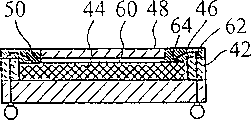
Consult Fig. 2, the utility model first embodiment, a kind of image sensor mainly comprises: a substrate 40, a flange layer 42, an image sensing wafer 44, plural wires 46, a photic zone 48 and an adhesive layer 50.
Substrate 40 is provided with first surface 54 and has the second surface 56 of signal output end 58, signal output end 58 is connected on the printed circuit board (PCB) (not shown) in order to electricity, the signal output end 58 grid array Metal Ball 59 (Ball GRIDARRAY) of can electricity receiving is connected on the printed circuit board (PCB) by ball grid array Metal Ball 59 electricity again in the present embodiment.
This plural wires 46 connects a plurality of weld pads 64 of image sensing wafer 44 to the signal input end 62 of flange layer 42 by this hollow out zone electricity.
Because the area of photic zone 48 is less than the area of groove 60, when making photic zone 48 be covered on the flange layer 42, be formed with a hollow out zone, and plural wires 46 is connected to flange layer 42 tops by this hollow out zone electricity, therefore, flange layer 42 can fully hold image sensing wafer 44 with substrate 40 formed grooves 60, and needn't reserve the space of making contact, make in the packaging body of certain size and can hold larger sized image sensing wafer, and plural wires 46 can not pressed by photic zone 48, can improve yields and convenience in the manufacturing.
Referring to Fig. 3, the utility model second embodiment, when the weld pad 64 of image sensing wafer 44 is positioned at both sides, photic zone 48 can be made into less area, when it is covered on the flange layer 42, make groove 60 both sides all be formed with the hollow out zone, and the weld pad 64 on the image sensing wafer 44, then expose, and plural wires 46 connects the signal input end 62 of the weld pad 64 of image sensing wafer 44 to flange layer 42 by this two hollow outs zone electricity by this two hollow outs zone.
Referring to Fig. 4, the utility model the 3rd embodiment, it is roughly identical with first embodiment, its difference is: this substrate 40 does not need to be provided with in addition signal output end 58, and transmit medium (present embodiment is a flexible circuit board 52) is connected to flange layer 42 with the hot pressing mode electricity signal input end 62 by one, after the signal that makes image sensing wafer 44 is passed to signal input end 62 on the flange layer 42 by plural wires 46, pass by flexible circuit board 52 again, and be covered in this hollow out zone with adhesive layer 50, in order to flexible circuit board 52 and plural wires 46 are covered.
Therefore, not only can be reduced on the substrate 40 processing procedure of making signal output end and save cost, but the more use of mat flexible circuit board 52, make image sensor very flexibly electricity be connected on the printed circuit board (PCB), make it more practical.
Referring to Fig. 5, the utility model the 4th embodiment, its difference is: it directly is connected to the employed flexible circuit board 52 of Fig. 4 on the weld pad 64 of image sensing wafer 44 with the hot pressing mode electricity, the signal of image sensing wafer 44 directly is passed on the flexible circuit board 52, therefore, the operation of needn't making contact separately in whole encapsulation process not only can be omitted the material cost of plural wires 46, and can simplify the whole operation of making contact, more practical in the use.
The above only is several preferred embodiment of the present utility model; be not to limit practical range of the present utility model with this; allly do various variations and modification, all should be covered by within the patent protection category that the utility model claims are defined according to spirit of the present utility model and principle.
Claims (6)
1. image sensor, it includes: a substrate, a flange layer, an image sensing wafer, plural wires, a photic zone and an adhesive layer; It is characterized in that:
One substrate, it is provided with first surface and second surface;
One flange layer, it is arranged on the first surface of this substrate and forms a groove with this substrate, and is formed with signal input end on it;
One image sensing wafer is provided with a plurality of weld pads, and it is arranged on the first surface of this substrate, and is positioned at this groove;
One photic zone, when being covered on this flange layer, this groove is formed with at least one hollow out zone, and a plurality of weld pads on this image sensing wafer are exposed by this hollow out zone;
Plural wires connects the signal input end of the weld pad of this image sensing wafer to flange layer by this hollow out zone electricity; And
One adhesive layer, it is covered in this hollow out zone this plural wires is covered.
2. image sensor according to claim 1 is characterized in that: when described photic zone was covered on this flange layer, this groove was formed with two hollow out zones, and the weld pad of this image sensing wafer is then exposed by these two hollow out zones respectively.
3. image sensor according to claim 1 is characterized in that: described photic zone is a transparent glass.
4. image sensor according to claim 1 is characterized in that: the second surface of described substrate is formed with signal output end, and electricity is connected to the signal input end on this flange layer.
5. image sensor according to claim 4 is characterized in that: the signal input end on the described flange layer connects this signal output end by the lead electricity that connects flange layer and substrate.
6. image sensor according to claim 4 is characterized in that: described signal output end can be connected with the ball grid array Metal Ball.
Priority Applications (1)
| Application Number | Priority Date | Filing Date | Title |
|---|---|---|---|
| CN 02281929 CN2587062Y (en) | 2002-10-17 | 2002-10-17 | image sensor |
Applications Claiming Priority (1)
| Application Number | Priority Date | Filing Date | Title |
|---|---|---|---|
| CN 02281929 CN2587062Y (en) | 2002-10-17 | 2002-10-17 | image sensor |
Publications (1)
| Publication Number | Publication Date |
|---|---|
| CN2587062Y true CN2587062Y (en) | 2003-11-19 |
Family
ID=33744154
Family Applications (1)
| Application Number | Title | Priority Date | Filing Date |
|---|---|---|---|
| CN 02281929 Expired - Fee Related CN2587062Y (en) | 2002-10-17 | 2002-10-17 | image sensor |
Country Status (1)
| Country | Link |
|---|---|
| CN (1) | CN2587062Y (en) |
-
2002
- 2002-10-17 CN CN 02281929 patent/CN2587062Y/en not_active Expired - Fee Related
Similar Documents
| Publication | Publication Date | Title |
|---|---|---|
| CN100517738C (en) | Package structure of image sensor chip | |
| CN2587062Y (en) | image sensor | |
| CN1272854C (en) | Image sensor and packaging method thereof | |
| CN2641822Y (en) | Integrated circuit package components | |
| US20040089906A1 (en) | Image sensor structure | |
| CN109103265B (en) | Photoelectric sensor packaging structure with cushion block and packaging method thereof | |
| WO2008138182A1 (en) | Chip type light-emitting diode | |
| CN201075390Y (en) | Photoreception crystal plate packaging module | |
| CN2598144Y (en) | Image sensor packaged by image sensing chip with transparent layer | |
| CN2585418Y (en) | Image Sensor Construction | |
| JPH01272144A (en) | Semiconductor device and assembly method thereof | |
| CN2465329Y (en) | an image sensor | |
| CN2691057Y (en) | Packaging structure of light sensing chip | |
| CN2471058Y (en) | Improved packaging device of image sensor | |
| CN2603517Y (en) | Semiconductor chip stacking structure | |
| CN101834162A (en) | Chip packaging structure and method | |
| CN2461152Y (en) | Packaged image sensor chip with light-transmitting sheet | |
| CN2636535Y (en) | Image sensor | |
| CN2612062Y (en) | Image sensor that is immune to side light interference | |
| CN2612072Y (en) | Displacement Wire Bonding Image Sensor Package Structure | |
| CN2470959Y (en) | stacked image sensor | |
| CN2463958Y (en) | Integrated circuit | |
| CN2612996Y (en) | Mod card with sheet metal | |
| CN2590178Y (en) | Integrated Integrated Circuit Stack Assembly | |
| CN2519418Y (en) | Image sensor |
Legal Events
| Date | Code | Title | Description |
|---|---|---|---|
| C14 | Grant of patent or utility model | ||
| GR01 | Patent grant | ||
| C17 | Cessation of patent right | ||
| CF01 | Termination of patent right due to non-payment of annual fee |
Granted publication date: 20031119 Termination date: 20091117 |