WO2018110887A1 - Heterocyclic compound, and organic light-emitting element comprising same - Google Patents
Heterocyclic compound, and organic light-emitting element comprising same Download PDFInfo
- Publication number
- WO2018110887A1 WO2018110887A1 PCT/KR2017/014194 KR2017014194W WO2018110887A1 WO 2018110887 A1 WO2018110887 A1 WO 2018110887A1 KR 2017014194 W KR2017014194 W KR 2017014194W WO 2018110887 A1 WO2018110887 A1 WO 2018110887A1
- Authority
- WO
- WIPO (PCT)
- Prior art keywords
- compound
- group
- light emitting
- deuterium
- layer
- Prior art date
- Legal status (The legal status is an assumption and is not a legal conclusion. Google has not performed a legal analysis and makes no representation as to the accuracy of the status listed.)
- Ceased
Links
- 0 *c1c(*c2c-3c(*)c(*)c(-c4c(cccc5)c5c(*)c5c4cccc5)c2I)c-3c(*)c(*)c1* Chemical compound *c1c(*c2c-3c(*)c(*)c(-c4c(cccc5)c5c(*)c5c4cccc5)c2I)c-3c(*)c(*)c1* 0.000 description 5
- AJPKWXXQSSNPPK-UHFFFAOYSA-N COc(c(O)c(c(O)c1O)O)c1O Chemical compound COc(c(O)c(c(O)c1O)O)c1O AJPKWXXQSSNPPK-UHFFFAOYSA-N 0.000 description 1
- ZESMJEXCDQKEMB-UHFFFAOYSA-N Cc(c(O)c(c(O)c1O)O)c1OC Chemical compound Cc(c(O)c(c(O)c1O)O)c1OC ZESMJEXCDQKEMB-UHFFFAOYSA-N 0.000 description 1
- FNMITDBDOJPWEW-UHFFFAOYSA-N Oc(c(-c1c(cccc2)c2cc2c1cccc2)c1O)c(c(c([o]2)c(c(O)c3O)O)c3O)c2c1O Chemical compound Oc(c(-c1c(cccc2)c2cc2c1cccc2)c1O)c(c(c([o]2)c(c(O)c3O)O)c3O)c2c1O FNMITDBDOJPWEW-UHFFFAOYSA-N 0.000 description 1
- ZHRJXWRYFGMIKU-UHFFFAOYSA-N Oc(c1c(c(-c2c(cccc3)c3c(-c3cc(cccc4)c4cc3)c3c2cccc3)c2O)[o]c(c(O)c3O)c1c(O)c3O)c2O Chemical compound Oc(c1c(c(-c2c(cccc3)c3c(-c3cc(cccc4)c4cc3)c3c2cccc3)c2O)[o]c(c(O)c3O)c1c(O)c3O)c2O ZHRJXWRYFGMIKU-UHFFFAOYSA-N 0.000 description 1
Classifications
-
- C—CHEMISTRY; METALLURGY
- C07—ORGANIC CHEMISTRY
- C07D—HETEROCYCLIC COMPOUNDS
- C07D307/00—Heterocyclic compounds containing five-membered rings having one oxygen atom as the only ring hetero atom
- C07D307/77—Heterocyclic compounds containing five-membered rings having one oxygen atom as the only ring hetero atom ortho- or peri-condensed with carbocyclic rings or ring systems
- C07D307/91—Dibenzofurans; Hydrogenated dibenzofurans
-
- H—ELECTRICITY
- H10—SEMICONDUCTOR DEVICES; ELECTRIC SOLID-STATE DEVICES NOT OTHERWISE PROVIDED FOR
- H10K—ORGANIC ELECTRIC SOLID-STATE DEVICES
- H10K85/00—Organic materials used in the body or electrodes of devices covered by this subclass
- H10K85/60—Organic compounds having low molecular weight
- H10K85/649—Aromatic compounds comprising a hetero atom
- H10K85/657—Polycyclic condensed heteroaromatic hydrocarbons
-
- C—CHEMISTRY; METALLURGY
- C07—ORGANIC CHEMISTRY
- C07D—HETEROCYCLIC COMPOUNDS
- C07D333/00—Heterocyclic compounds containing five-membered rings having one sulfur atom as the only ring hetero atom
- C07D333/50—Heterocyclic compounds containing five-membered rings having one sulfur atom as the only ring hetero atom condensed with carbocyclic rings or ring systems
- C07D333/76—Dibenzothiophenes
-
- C—CHEMISTRY; METALLURGY
- C09—DYES; PAINTS; POLISHES; NATURAL RESINS; ADHESIVES; COMPOSITIONS NOT OTHERWISE PROVIDED FOR; APPLICATIONS OF MATERIALS NOT OTHERWISE PROVIDED FOR
- C09K—MATERIALS FOR MISCELLANEOUS APPLICATIONS, NOT PROVIDED FOR ELSEWHERE
- C09K11/00—Luminescent, e.g. electroluminescent, chemiluminescent materials
- C09K11/06—Luminescent, e.g. electroluminescent, chemiluminescent materials containing organic luminescent materials
-
- H—ELECTRICITY
- H10—SEMICONDUCTOR DEVICES; ELECTRIC SOLID-STATE DEVICES NOT OTHERWISE PROVIDED FOR
- H10K—ORGANIC ELECTRIC SOLID-STATE DEVICES
- H10K85/00—Organic materials used in the body or electrodes of devices covered by this subclass
- H10K85/60—Organic compounds having low molecular weight
- H10K85/649—Aromatic compounds comprising a hetero atom
- H10K85/657—Polycyclic condensed heteroaromatic hydrocarbons
- H10K85/6574—Polycyclic condensed heteroaromatic hydrocarbons comprising only oxygen in the heteroaromatic polycondensed ring system, e.g. cumarine dyes
-
- H—ELECTRICITY
- H10—SEMICONDUCTOR DEVICES; ELECTRIC SOLID-STATE DEVICES NOT OTHERWISE PROVIDED FOR
- H10K—ORGANIC ELECTRIC SOLID-STATE DEVICES
- H10K85/00—Organic materials used in the body or electrodes of devices covered by this subclass
- H10K85/60—Organic compounds having low molecular weight
- H10K85/649—Aromatic compounds comprising a hetero atom
- H10K85/657—Polycyclic condensed heteroaromatic hydrocarbons
- H10K85/6576—Polycyclic condensed heteroaromatic hydrocarbons comprising only sulfur in the heteroaromatic polycondensed ring system, e.g. benzothiophene
-
- C—CHEMISTRY; METALLURGY
- C09—DYES; PAINTS; POLISHES; NATURAL RESINS; ADHESIVES; COMPOSITIONS NOT OTHERWISE PROVIDED FOR; APPLICATIONS OF MATERIALS NOT OTHERWISE PROVIDED FOR
- C09K—MATERIALS FOR MISCELLANEOUS APPLICATIONS, NOT PROVIDED FOR ELSEWHERE
- C09K2211/00—Chemical nature of organic luminescent or tenebrescent compounds
- C09K2211/10—Non-macromolecular compounds
- C09K2211/1018—Heterocyclic compounds
- C09K2211/1025—Heterocyclic compounds characterised by ligands
- C09K2211/1088—Heterocyclic compounds characterised by ligands containing oxygen as the only heteroatom
-
- C—CHEMISTRY; METALLURGY
- C09—DYES; PAINTS; POLISHES; NATURAL RESINS; ADHESIVES; COMPOSITIONS NOT OTHERWISE PROVIDED FOR; APPLICATIONS OF MATERIALS NOT OTHERWISE PROVIDED FOR
- C09K—MATERIALS FOR MISCELLANEOUS APPLICATIONS, NOT PROVIDED FOR ELSEWHERE
- C09K2211/00—Chemical nature of organic luminescent or tenebrescent compounds
- C09K2211/10—Non-macromolecular compounds
- C09K2211/1018—Heterocyclic compounds
- C09K2211/1025—Heterocyclic compounds characterised by ligands
- C09K2211/1092—Heterocyclic compounds characterised by ligands containing sulfur as the only heteroatom
-
- H—ELECTRICITY
- H10—SEMICONDUCTOR DEVICES; ELECTRIC SOLID-STATE DEVICES NOT OTHERWISE PROVIDED FOR
- H10K—ORGANIC ELECTRIC SOLID-STATE DEVICES
- H10K50/00—Organic light-emitting devices
- H10K50/10—OLEDs or polymer light-emitting diodes [PLED]
- H10K50/11—OLEDs or polymer light-emitting diodes [PLED] characterised by the electroluminescent [EL] layers
Definitions
- the present invention relates to a heterocyclic compound having a novel structure and an organic light emitting device including the same.
- organic light emitting phenomenon refers to a phenomenon of converting electrical energy into light energy using an organic material.
- the organic light emitting device using the organic light emitting phenomenon has a wide viewing angle, excellent contrast, fast response time, brightness, driving voltage and Many studies have been conducted because of excellent response speed characteristics.
- the organic light emitting device generally has a structure including an anode and a cathode and an organic layer between the anode and the cathode.
- the organic material charge is often composed of a multilayer structure composed of different materials, for example, a hole injection layer, a hole transport layer, a light emitting layer, and an electron transport insect. It may be made of an electron injection insect.
- Patent Document 0001 Korean Patent Publication No. 2000-0051826
- the present invention relates to a heterocyclic compound having a novel structure and an organic light emitting device including the same.
- the present invention provides a compound represented by the following formula (1).
- X is 0 or S
- Ri to 3 ⁇ 4 are each independently hydrogen or deuterium, at least one of 3 ⁇ 4 to is deuterium, and any one of to R 4 is the following Chemical Formula 2,
- the present invention is a first electrode; A second electrode provided to face the first electrode; And at least one organic layer disposed between the first electrode and the second electrode, wherein at least one of the organic layers includes a compound represented by Chemical Formula 1. to provide.
- the compound represented by Chemical Formula 1 may be used in the organic material layer of the organic light emitting device. It can be used as a material, and can improve efficiency, low driving voltage and / or lifespan characteristics in the organic light emitting device.
- the compound represented by Formula 1 may be used as a hole injection, hole transport, hole injection and transport, light emission, electron transport, or electron injection material, in particular can be used as a blue light emitting material.
- FIG. 1 shows an example of an organic light emitting element composed of a substrate 1, an anode 2, a light emitting layer 3, and a cathode 4.
- FIG. 2 shows a substrate 1, an anode 2, a hole injection layer 5, and a hole transport layer 6.
- the example of the organic light emitting element which consists of the light emitting layer 7, the electron carrying layer 8, and the cathode 4 is shown.
- substituted or unsubstituted may mean substituted or unsubstituted by R a , ⁇ is deuterium, halogen, cyano group, nitro group, amino group, alkyl group having 1 to 40 carbon atoms, carbon number At least one of 1 to 40 haloalkyl group, substituted or unsubstituted 0, N, Si and S containing at least one heteroalkyl group having 1 to 40 carbon atoms, substituted or unsubstituted 0, N, Si and S It may include a heterohaloalkyl group having 1 to 40 carbon atoms, or an alkenyl group having 2 to 40 carbon atoms
- the halogen may be fluorine, chlorine, bromine or iodine.
- an alkyl group having 1 to 40 carbon atoms may be a straight chain alkyl group having 1 to 40 carbon atoms; a straight chain alkyl group having 1 to 20 carbon atoms; Linear alkyl groups of 1 to 10; Branched or cyclic alkyl groups having 3 to 40 carbon atoms; Branched or cyclic alkyl groups having 3 to 20 carbon atoms; Or a branched or cyclic alkyl group having 3 to 10 carbon atoms.
- the alkyl group having 1 to 40 carbon atoms is methyl group, ethyl group, n—propyl group, i so-propyl group, n-butyl group, i so-butyl group, t-butyl group, n-pentyl group, i so- Pentyl group, neo-pentyl group or cyclonuclear group.
- the present invention is not limited thereto.
- the heteroalkyl group having 1 to 40 carbon atoms is each independently one or more carbon atoms of 0, N. It may be substituted with Si or S.
- a heteroalkyl group in which carbon number 1 of the n-butyl group is substituted with 0 is an n-propoxy group
- a heteroalkyl group substituted with N is an n ⁇ propylamino group
- a heteroalkyl group substituted with Si is n Is a propylsilyl group
- the heteroalkyl group substituted with S is an n-propylthio group.
- the heteroalkyl group in which the carbon number 1 of the neo-pentyl group is substituted with 0 is a t-butoxy group
- the heteroalkyl group substituted with N is a t -butylamino group
- the heteroalkyl group substituted with Si is t A -butylsilyl group
- the heteroalkyl group substituted with S is a t-butylthio group.
- the heteroalkyl group in which the carbon number 2 of the cyclonuclear group is substituted with 0 is 2-tetrahydropyranyl group
- the heteroalkyl group substituted with N is 2-piperidinyl group.
- a heterocyclic group substituted by Si 1-sila-and haeksil (1-si la- cyc lohexyl) based upon a ⁇ cycles, the heteroaryl group is substituted by S 2-thio-tetrahydro pyranyl (2-tetrahydrothiopyranyl) group is .
- the heteroalkyl group having 1 to 40 carbon atoms has a straight, branched or cyclic hydroxyalkyl group having 1 to 40 carbon atoms; Linear, branched or cyclic alkoxy groups having 1 to 40 carbon atoms; Linear, branched or cyclic alkoxyalkyl groups having 2 to 40 carbon atoms; Linear, branched or cyclic aminoalkyl groups having 1 to 40 carbon atoms; Linear, branched or cyclic alkylamino groups having 1 to 40 carbon atoms; Linear, branched or cyclic alkylaminoalkyl groups having 1 to 40 carbon atoms; Linear, branched or cyclic silylalkyl (oxy) groups having 1 to 40 carbon atoms; Linear, branched or cyclic alkyl (oxy) silyl groups having 1 to 40 carbon atoms; Straight chain, branched chain of 1 to 40 carbon atoms, or Cyclic alkyl (oxy) silic al
- the heteroalkyl group having 1 to 40 carbon atoms has a hydroxymethyl group, a methoxy group, an ethoxy group, ⁇ -propoxy group, i so-propoxy group, t-subspecial group, cyclonuclear special group, mesospecial methyl group, i so -Propoxymethyl group, cyclonucleooxymethyl group, 2-tetrahydropyranyl (l-tetr ahydr opyr any l) 7 l, aminomethyl group, methylamino group, ⁇ -propylamino group, t-butylamino group ⁇ methylaminopropyl group, 2- Piperidinyl group, n-propylsilyl group.
- an alkenyl group having 2 to 40 carbon atoms may be a straight chain, branched chain or cyclic alkenyl group.
- the alkenyl group having 2 to 40 carbon atoms has a straight chain alkenyl group having 2 to 40 carbon atoms; Linear alkenyl groups having 2 to 20 carbon atoms; Linear alkenyl groups having 2 to 10 carbon atoms; Branched alkenyl groups having 3 to 40 carbon atoms; Branched alkenyl groups having 3 to 20 carbon atoms; Branched alkenyl groups having 3 to 10 carbon atoms; Cyclic alkenyl groups having 5 to 40 carbon atoms; Cyclic alkenyl groups having 5 to 20 carbon atoms; Or a cyclic alkenyl group having 5 to 10 carbon atoms.
- the alkenyl group having 2 to 40 carbon atoms may be an ethenyl group, propenyl group, butenyl group, pentenyl group, or cyclonucleenyl group.
- the present invention is not limited thereto.
- the aryl group having 6 to 20 carbon atoms may be a monocyclic aryl group or a polycyclic aryl group.
- the aryl group having 6 to 20 carbon atoms may be a phenyl group, a biphenyl group or a terphenyl group as a monocyclic aryl group, and a naphthyl group, anthracenyl group, phenanthryl group, triphenylenyl group, pyrenyl group as a polycyclic aryl group. It may be a perrylenyl group, chrysenyl group or fluorenyl group.
- the aryl group having 6 to 20 carbon atoms may have a structure in which two or more selected from the group consisting of a monocyclic aryl group and a polycyclic aryl group are connected to each other.
- the aryl group having 6 to 20 carbon atoms may have a structure in which a polycyclic aryl group and / or a monocyclic aryl group are linked to the polycyclic aryl group. More specifically, the aryl group having 6 to 20 carbon atoms may be a naphthylphenyl group, anthracenylphenyl group phenanthrylphenyl group, fluorenylphenyl group, phenylnaphthyl group or phenylanthracenyl group. However, the present invention is not limited thereto. In the present specification, the fluorenyl group may be substituted, two substituents are bonded to each other
- the present invention provides a compound represented by Formula 1 in the present invention. If hayeoteul used as a light emitting layer host material of dibenzofuran or dibenzothiophene when directly bonded to anthracene increases the HOMO Highest Occupi ed Mo l ecu l ar Orbi tal) energy rebael of molecular organic light-emitting device is represented by Formula 1, "hole In addition, it is possible to reduce the driving voltage by smoothly injecting In addition, in the case of Ar1 CUHM aryl group, the thermal stability is increased, so that the molecular weight is suitable for thermal vacuum deposition, and stability in the manufacturing process of the organic light emitting device can be ensured.
- R and R 3 to 3 ⁇ 4 are each independently hydrogen or deuterium. And at least one of R 8 is deuterium,
- R 2 to 3 ⁇ 4 are each independently hydrogen or deuterium, at least one of 3 ⁇ 4 to 3 ⁇ 4 is deuterium,
- Formula 1-3 and 3 ⁇ 4 to 3 ⁇ 4 are each independently hydrogen or deuterium, at least one of 3 ⁇ 4, R 2 and R 4 to 3 ⁇ 4 is deuterium,
- R 3 and R 8 are each independently hydrogen or deuterium, at least one of ⁇ to 3 ⁇ 4 and to 3 ⁇ 4 is deuterium.
- ⁇ to 3 ⁇ 4 and to 3 ⁇ 4 is deuterium.
- 3 ⁇ 4; R 4 ; R 5 ; ; R 7 ; R 8 ; i and; Re and; Ri, 3 and; 5 to; Or Ri and R 3 to R 8 are deuterium, with the remainder being hydrogen.
- the In Formula 1-1 and R 3 to R 8 Rs and R 4 ; R 5 to; Or 3 ⁇ 4 and R 3 to R 8 are deuterium and the remainder is hydrogen.
- R 2 ; R 3 ; R 4 ; R 5 ; R 6 ; R 7 ; R 8 ; R 2 and 3 ⁇ 4; R 6 and R 8 ; R 2 to; To; Or 3 ⁇ 4 to 3 ⁇ 4 is deuterium and the remainder is hydrogen. More preferably, in Formula 1-2, R 2 to 3 ⁇ 4; R 5 to R 8 ; Or R 2 to R 8 are deuterium, and the remainder are hydrogen. Also preferably, in Formulas 1-3 of R 1 R 2 and R 4 ,
- Ri; ; ; ; R 6 ; R 7 ; ; 2 and 4 ; R 6 and 3 ⁇ 4; Ri, R 2 and R 4 ; R 5 to or, and to 3 ⁇ 4 are deuterium and the remainder is hydrogen. More preferably, in Formulas 1-3, R 2 and R 4 to, Ri, R 2 and; R 5 to R 8 ; Or, R 2 and R 4 to 3 ⁇ 4 are deuterium and the remainder is hydrogen. Also preferably, among Formulas 1-4 and R 5 to R 8 , R, ..; R 2 ; 3 ⁇ 4; R 5 ; R 6 ; 7 ; ; Ri and 3 ⁇ 4: ' 3 ⁇ 4 and R 8 ; Ri to R 3 ; R 5 to ' .
- R 3 and R 5 to R 8 deuterium, with the remainder being hydrogen. More preferably.
- A is naphthyl, phenylnaphthyl, phenanthrenyl, or triphenylenyl.
- the compound represented by Formula 1 may be selected from the group consisting of the following compounds:
- the compound represented by Chemical Formula 1-1 may be prepared by the same method as in Scheme 1 below, and may be applied to Chemical Formulas 1, 1-2, 1-3, and 1-4. Can be.
- the present invention provides an organic light emitting device including the compound represented by Formula 1.
- the present invention comprises a first electrode; A second electrode provided to face the first electrode; And at least one organic material layer provided between the first electrode and the second electrode, wherein at least one of the organic material layers comprises a compound represented by Chemical Formula 1. do.
- the organic material layer of the organic light emitting device of the present invention may have a single layer structure, but may have a multi-layer structure in which two or more layers of organic material packs are stacked.
- the organic light emitting device of the present invention may have a structure including a hole injection layer, a hole transport layer, a light emitting layer, an electron transport layer, an electron injection layer and the like as the organic layer.
- the structure of the organic light emitting device is not limited thereto and may include a smaller number of organic layers.
- the organic layer may include a hole injection layer, a hole transport layer, or a layer for simultaneously injecting and transporting holes, the hole injection layer, holes
- the transport layer, or the layer for simultaneously injecting and transporting a hole may include the compound represented by Chemical Formula 1.
- the organic layer may include a light emitting insect, and the light emitting layer may include a compound represented by Chemical Formula 1.
- the organic layer may include an electron transport layer, an electron injection layer, or a layer for simultaneously transporting and injecting electrons, and the electron transport layer, an electron injection layer, or a layer for simultaneously transporting and injecting electrons may be represented by Formula 1 above. It may include a compound represented.
- the organic light emitting device according to the present invention may be an organic light emitting device having a structure in which an anode, one or more organic material layers, and a cathode are sequentially stacked: on a substrate.
- the organic light emitting device according to the present invention may be an organic light emitting device of an inverted type in which a cathode, one or more organic material layers, and an anode are sequentially stacked on a substrate.
- FIGS. 1 and 2 the structure of an organic light emitting device according to an embodiment of the present invention is illustrated in FIGS. 1 and 2.
- FIG. 1 shows an example of an organic light emitting element composed of a substrate 1, an anode 2, a light emitting insect 3, and a cathode 4.
- the compound represented by Formula 1 may be included in the light emitting layer.
- FIG. 2 shows an example of an organic light emitting element consisting of a substrate 1, an anode 2, a hole injection layer 5, a hole transport layer 6, a light emitting layer 7, an electron transport layer 8 and a cathode 4 It is.
- the compound represented by Formula 1 may be included in one or more layers of the hole injection layer, the hole transport layer, the light emitting layer and the electron transport layer.
- the organic light emitting device according to the present invention except that at least one layer of the organic material layer comprises a compound represented by the formula (1) It may be made of materials and methods known in the art.
- the organic material layers may be formed of the same material or different materials.
- the organic light emitting device according to the present invention may be manufactured by sequentially stacking a first electrode, an organic material layer, and a second electrode on a substrate.
- a metal oxide or a metal oxide having a conductivity or a metal on a substrate by using a physical vapor deposition deposition (PVD) method such as sputtering or e-beam evaporat ion
- PVD physical vapor deposition deposition
- An alloy is deposited to form an anode, and an organic material layer including a hole injection layer, a hole transport layer, a light emitting layer, and an electron transport insect may be formed thereon, and then, a material usable as a cathode may be deposited thereon.
- an organic light emitting device may be manufactured by sequentially depositing a cathode material, an organic material layer, and an anode material on a substrate. Also.
- the compound represented by Chemical Formula 1 may be formed into an organic material charge by a solution coating method as well as a vacuum deposition method in manufacturing an organic light emitting device.
- the solution coating method is spin coating, dip coating, doctor blading. Inkjet printing, screen printing, spraying, roll coating and the like, but is not limited to these.
- an organic light emitting device may be manufactured by sequentially depositing an organic material charge and an anode material from a cathode material on a substrate 0V0 2003/012890).
- the manufacturing method is not limited thereto.
- the first electrode is an anode
- the second electrode is a cathode
- the first electrode is a cathode
- the second electrode is an anode.
- the anode material a material having a large work function is generally preferred to facilitate hole injection into the organic material layer.
- the positive electrode material Metals such as vanadium, chromium, copper, zinc and gold or alloys thereof; Metal oxides such as zinc oxide, indium oxide, indium tin oxide (IT0), indium zinc oxide (IZ0); ⁇ ⁇ 0: A1 or SN0 2 : a combination of a metal and an oxide such as Sb; Conductive polymers such as poly (3-methylthiophene), poly [3,4- (ethylene-1,2-dioxy) thiophene KPED0T), polypyri and polyaniline, and the like, but are not limited thereto. It is preferable that the cathode material is a material having a small work function to facilitate electron injection into the organic material layer.
- the negative electrode material examples include magnesium, calcium, sodium, potassium, titanium, indium, and yttrium.
- Metals such as lithium, gadolinium, aluminum, silver, tin and lead or alloys thereof; Multilayer structure materials such as LiF / Al or U3 ⁇ 4 / A1, and the like, but are not limited thereto.
- the hole injection layer is a layer for injecting holes from the electrode.
- the hole injection material has a capability of transporting holes, and has excellent hole injection effects at the anode, and excellent holes for light emitting or light emitting materials.
- the compound which has an injection effect prevents the movement of the excitons which generate
- the hole injecting material is a metal porphyrin (porphyr in), oligothiophene, arylamine series of organic matter, hex nitrile hex-aza triphenylene ⁇ organic substance in the series, quinacridone (qu inacr i done) organic substance in the series, Fe Perylene organic materials, anthraquinone and polyaniline and polythiophene-based conductive polymers, but are not limited thereto.
- the hole transport layer is a material that receives holes from the hole injection layer and transports holes to the light emitting layer.
- the hole transport layer is a material that can transport holes from an anode or a hole injection layer to a light emitting layer as a hole transport material.
- the light emitting material is a material capable of emitting light in the visible region by transporting and combining holes and electrons from the hole transport layer and the electron transport layer, respectively, and a material having good quantum efficiency with respect to fluorescence or phosphorescence is preferable.
- the light emitting layer may include a host material and a dopant material.
- the host material is a condensed aromatic ring derivative or a heterocyclic containing compound. Specifically.
- Condensed aromatic ring derivatives include anthracene derivatives, pyrene derivatives, naphthalene derivatives, pentacene derivatives, and phenanthrene compounds. And pulluloranthene compounds.
- Heterocyclic containing compounds include, but are not limited to carbazole derivatives, dibenzofuran derivatives, ladder type furan compounds, pyrimidine derivatives, and the like.
- the light emitting layer may include a compound represented by Formula 1 as the host material.
- the dopant materials include aromatic amine derivatives, styrylamine compounds, boron complex 1, fluoranthene compounds, metal complexes, and the like.
- the aromatic amine derivative is a condensed aromatic ring derivative having a substituted or unsubstituted arylamino group, and includes pyrene, anthracene, chrysene and periplanthene having an arylamino group.
- the styrylamine compound is a compound in which at least one arylvinyl group is substituted with a substituted or unsubstituted arylamine, and an aryl group and a silyl group. Alkyl group.
- One or two or more substituents selected from the group consisting of a cycloalkyl group and an arylamino group are substituted or unsubstituted.
- substituents selected from the group consisting of a cycloalkyl group and an arylamino group are substituted or unsubstituted.
- styryl amine, styryl diamine styryl triamine, styryl tetraamine and the like but is not limited thereto.
- the metal complex includes a lychee complex, a back complex, and the like, but is not limited thereto.
- the electron transport layer is a layer that receives electrons from the electron injection charge and transports the electrons to the light emitting charge
- the electron transport material is a material that can inject electrons well from the cathode and transfer them to the light emitting layer. Suitable.
- the electron transport layer can be used with any desired cathode material as used in accordance with the prior art.
- suitable cathode materials are conventional materials having a low work function followed by an aluminum layer or silver worm. Specifically, cesium, barium, calcium, ytterbium and samarium, in each case followed by an aluminum worm or silver layer.
- the electron injection layer is a layer for injecting electrons from an electrode, has a capability of transporting electrons, has an electron injection effect from the cathode, excellent electron injection effect to the light emitting layer or the light emitting material, and hole injection of excitons generated in the light emitting layer
- the compound which prevents the movement to a layer and is excellent in thin film formation ability is preferable. Specifically, fluorenone, anthraquinodimethane, diphenoquinone. Thiopyran dioxide, oxazole, oxadiazole.
- Triazole imidazole, perylene tetracarboxylic acid, preorenylidene methane, anthrone and the like, derivatives thereof, metal complex compounds and nitrogen-containing five-membered ring derivatives, and the like, but are not limited thereto.
- 8-hydroxyquinolinato lithium bis (8- Hydroxyquinolinato zinc, bis (8-hydroxyquinolinato) copper, bis (8-hydroxyquinolinato) manganese, tris (8-hydroxyquinolinato) aluminum, tris (2-methyl- 8-hydroxyquinolinato) aluminum, tris (8-hydroxyquinolinato) gallium, bis (10-hydroxybenzo [h] quinolinato) beryllium, bis (10-hydroxybenzo [h] quinolina Earth, zinc, bis (2-methyl-8-quinolinato) chlorogallium, bis (2-methyl-8-quinolinato) (0-crezolato) gallium, bis (2-methyl-8-quinolinato) ) (1-naphtholato) aluminum, bis (2-methyl-8-quinolinato) (2-naphtholato) gallium, and the like.
- the organic light emitting device may be a top emission type, a bottom emission type or a double-sided emission type depending on the material used.
- the compound represented by Formula 1 may be included in an organic solar cell or an organic transistor in addition to the organic light emitting device. Preparation of the compound represented by Chemical Formula 1 and an organic light emitting device including the same will be described in detail in the following Examples. However, the following examples are intended to illustrate the present invention, and the scope of the present invention is not limited thereto.
- Dibenzo [b, d] furan-d8 (50.0 g, 283.7 ⁇ 0 1) was dissolved in THF (500 ml) under a nitrogen atmosphere in a dried three-necked flask and 1.6M n-butyl with stirring at -78 ° C. Lithium (186 ml, 297.9 mniol) was slowly added dropwise. When the dropwise addition was completed, the mixture was stirred for 1 hour while maintaining at -78 ° C. Thereafter, trimethyl borate (38.3 g, 368.8 Pa ol) was slowly added dropwise, and then raised to room temperature and stirred for 1 hour.
- 1,3-dimethoxybenzene—2, 4, 5,6 ⁇ 14 (50.0 g, 351.6 ⁇ ol) was dissolved in THF (500 ml) under a nitrogen atmosphere in a dried three-neck flask at -10 ° C.
- 1.6 M n-butyllithium (231 ml, 369.2 ⁇ ol) was slowly added dropwise with stirring, after which the addition was completed, the mixture was stirred for 4 more hours at the same degree, and then cooled to -78 ° C and trimethyl borate (47.5 g, 457.1 mniol) was slowly added dropwise, followed by stirring overnight at room temperature. After reaction was completed, 2N HC1 aqueous solution was added dropwise.
- Example 5 Preparation of Compound 5
- Example 7 Preparation of Compound 7
- Step 4 of Example 1 except that Compound 5-b was used instead of Compound 1-c and (6-phenylnaphthalen-2-yl) boronic acid was used instead of naphthalen-2-ylboronic acid, Compound 7 was prepared by the same method as the preparation method (5.0 g, yield 31%, MS: M + H] + -554).
- Example 9 Preparation of Compound 9
- Step 3 of Example 1, except that Compound 9-a was used instead of Compound 1-b, Compound 9-b was prepared by the same method as the method for preparing Compound 1-c (11.9 g, yield 88%, MS: [M + H] + 426). Step 3) Preparation of Compound '9
- Example 11 Preparation of Compound 11
- Step 3 of Example 1, except that Compound 11-a was used instead of Compound 1-b, Compound 11-b was prepared by the same method as the method for preparing Compound 1-c (11.5 g, 85% yield, MS: [M + H] + 426).
- IT0 Indium Tin Oxide
- IT0 Indium Tin Oxide
- Fischer Co.'s Decon TM C0N705 product was used as a detergent, and distilled water was filtered secondly with a 0.22 sterilizing filter of Millerpore Co.'s product.
- the ultrasonic cleaning was performed twice with distilled water for 10 minutes.
- ultrasonic washing with a solvent of isopropyl alcohol, acetone and methanol for 10 minutes, dried and then transported to a plasma cleaner.
- the substrate was cleaned for 5 minutes using an oxygen plasma, and then the substrate was transferred to a vacuum evaporator.
- the following HI— ⁇ compound and the following HAT ′ CN compound were thermally vacuum deposited to a thickness of 650 A and a thickness of 50 A, respectively, on the ⁇ transparent electrode thus prepared to form a hole injection layer.
- the following HT-A compound was vacuum deposited to a thickness of 600 A on the hole injection layer to form a hole transport layer.
- the following HT—B compound was thermally vacuum deposited to a thickness of 50 A on the hole transport layer to form an electron blocking layer.
- the light emitting layer was formed by vacuum depositing Compound 1 and the following BD compound on the electronic blocking layer at a thickness of 200 A at a weight ratio of 96: 4.
- the following ET-A compound was vacuum-deposited to a thickness of 50 A on the luminescent charge to form a hole blocking layer.
- the following ET-B compound and the following Liq compound were thermally vacuum-deposited to a thickness of 310 A on a weight ratio of 1: 1 to form an electron transport layer on the hole blocking layer.
- the following L iq compound was vacuum deposited to a thickness of 5 A on the electron transport layer to form an electron injection layer.
- Magnesium and silver were sequentially deposited on the electron injection layer at a weight ratio of 10: 1 to 120A, and aluminum was deposited to 1000A to form a cathode, thereby manufacturing an organic light emitting device.
- BH-D increased molecular weight by introducing substituent 3 ⁇ 4 to dibenzofuran to ensure thermal stability.
- Comparative Experimental Example 5 and Comparative Experimental Example 6 are . Rather, it resulted in higher voltage, lower efficiency, and lower lifetime.
- a dibenzofuran or a dibenzothiophene is directly bonded to anthracene, and an aryl group having 10 to 20 carbon atoms is opposite to the blue light emitting layer host. have.
- deuterium has a higher atomic weight than hydrogen and thus has a small oscillation mode, which increases the non-radioactive decay time in the excited state, and in particular, increases the stability of the triplet excitons.
- the increased stability of triplet excitons can eventually amplify the TTF phenomenon and contribute to the efficiency and lifetime improvement of blue fluorescence.
- the results of Experimental Examples 1 to 15 described in Table 1 show such effects well when compared with Comparative Experimental Example 7 and Comparative Experimental Example 8 in which deuterium is not substituted. From the results of the experimental examples, the more deuterium is contained in dibenzofuran or dibenzothiophene, the more the deuterium is located in the anthracene where the triplet excitons are mainly located. The closer it is, the greater the effect.
- the material having the structure of Formula 1 is used as the blue light emitting layer host of the organic electroluminescent device, a low voltage, high efficiency, long life device can be obtained.
- substrate 2 anode
Landscapes
- Chemical & Material Sciences (AREA)
- Organic Chemistry (AREA)
- Engineering & Computer Science (AREA)
- Materials Engineering (AREA)
- Physics & Mathematics (AREA)
- Spectroscopy & Molecular Physics (AREA)
- Electroluminescent Light Sources (AREA)
Abstract
Description
【발명의 명칭】 [Name of invention]
헤테로 고리 화합물 및 이를 포함하는 유기 발광 소자 Heterocyclic compound and organic light emitting device comprising the same
【기술분야】 Technical Field
관련 출원 (들)과의 상호 인용 Cross Citation with Related Application (s)
본 출원은 2016년 12월 14일자 한국 특허 출원 제 10-2016- This application is filed with Korean Patent Application No. 10-2016-
0170676호에 기초한 우선권의 이익을 주장하며ᅳ 해당 한국 특허 출원의 문헌에 개시된 모든 내용은 본 명세서의 일부로서 포함된다. 본 발명은 신규한 구조의 헤테로 고리 화합물 및 이를 포함하는 유기 발광 소자에 관한 것이다. Claiming the benefit of priority based on 0170676, all the contents disclosed in the literature of the relevant Korean patent application are incorporated as part of this specification. The present invention relates to a heterocyclic compound having a novel structure and an organic light emitting device including the same.
【배경기술】 Background Art
일반적으로 유기 발광 현상이란 유기 물질을 이용하여 전기에너지를 빛쎄너지로 전환시켜주는 현상을 말한다ᅳ 유기 발광 현상을 이용하는 유기 발광 소자는 넓은 시야각, 우수한 콘트라스트, 빠른 웅답 시간을 가지며, 휘도, 구동 전압 및 응답 속도 특성이 우수하여 많은 연구가 진행되고 있다. 유기 발광 소자는 일반적으로 양극과 음극 및 상기 양극과 음극 사이에 유기물 층을 포함하는 구조를 가진다. 상기 유기물 충은 유기 발광 소자의 효율과 안정성을 높이기 위하여 각기 다른 물질로 구성된 다층의 구조로 이루어진 경우가 많으며, 예컨대 정공 주입층, 정공 수송층, 발광층, 전자 수송충. 전자 주입충 등으로 이루어질 수 있다. 이러한 유기 발광 소자의 구조에서 두 전극 사이에 전압을 걸어주게 되면 양극에서는 정공이, 음극에서는 전자가 유기물 층에 주입되게 되고, 주입된 정공과 전자가 만났을 때 엑시톤 (exc i ton)이 형성되며, 이 액시톤이 다시 바닥상태로 떨어질 때 빛이 나게 된다. 상기와 같은 유기 발광 소자에 사용되는 유기물에 대하여 새로운 재료의 개발이 지속적으로 요구되고 있다. In general, organic light emitting phenomenon refers to a phenomenon of converting electrical energy into light energy using an organic material. The organic light emitting device using the organic light emitting phenomenon has a wide viewing angle, excellent contrast, fast response time, brightness, driving voltage and Many studies have been conducted because of excellent response speed characteristics. The organic light emitting device generally has a structure including an anode and a cathode and an organic layer between the anode and the cathode. In order to increase the efficiency and stability of the organic light emitting device, the organic material charge is often composed of a multilayer structure composed of different materials, for example, a hole injection layer, a hole transport layer, a light emitting layer, and an electron transport insect. It may be made of an electron injection insect. When the voltage is applied between the two electrodes in the structure of the organic light emitting device, holes are injected into the organic material layer at the anode, electrons are injected into the organic layer, and excitons are formed when the injected holes and the electrons meet each other. The axtone glows when it falls back to the ground. There is a continuous demand for the development of new materials for organic materials used in such organic light emitting devices.
【선행기술문헌】 Prior Art Documents
【특허문헌】 (특허문헌 0001) 한국특허 공개번호 제 1으 2000-0051826호 [Patent literature] (Patent Document 0001) Korean Patent Publication No. 2000-0051826
【발명의 내용】 [Content of invention]
【해결하려는 과제】 [Problem to solve]
본 발명은 신규한 구조의 헤테로 고리 화합물 및 이를 포함하는 유기 발광 소자에 관한 것이다. The present invention relates to a heterocyclic compound having a novel structure and an organic light emitting device including the same.
[과제의 해결 수단】 [Solution of problem]
본 발명은 하기 화학식 1로 표시되는 화합물을 제공한다. The present invention provides a compound represented by the following formula (1).

상기 화학식 1에서, In Chemical Formula 1,
X는 0또는 S이고, X is 0 or S,
Ri 내지 ¾은 각각 독립적으로 수소 또는 중수소이되, ¾ 내지 중 적어도 하나는 중수소、이고, 내지 R4 중 어느 하나는 하기 화학식 2이며, Ri to ¾ are each independently hydrogen or deuterium, at least one of ¾ to is deuterium, and any one of to R 4 is the following Chemical Formula 2,

八!^은 치환 또는 비치환된 C10-20 아릴이다. 또한, 본 발명은 제 1 전극; 상기 제 1 전극과 대향하여 구비된 제 2 전극; 및 상기 제 1 전극과 상기 제 2 전극 사이에 구비된 1층 이상의 유기물 층을 포함하는 유기 발광 소자로서 , 상기 유기물 층 중 1층 이상은 상기 화학식 1로 표시되는 화합물을 포함하는, 유기 발광 소자를 제공한다. !八^ is substituted or unsubstituted C 10 - 20 is aryl. In addition, the present invention is a first electrode; A second electrode provided to face the first electrode; And at least one organic layer disposed between the first electrode and the second electrode, wherein at least one of the organic layers includes a compound represented by Chemical Formula 1. to provide.
【발명의 효과】 【Effects of the Invention】
상술한 화학식 1로 표시되는 화합물은 유기 발광 소자의 유기물 층의 재료로서 사용될 수 있으며, 유기 발광 소자에서 효율의 향상, 낮은 구동전압 및 /또는 수명 특성을 향상시킬 수 있다. 상술한 화학식 1로 표시되는 화합물은 정공 주입, 정공 수송, 정공 주입 및 수송, 발광, 전자 수송, 또는 전자 주입 재료로 사용될 수 있으며, 특히 청색 발광 재료로 사용될 수 있다. The compound represented by Chemical Formula 1 may be used in the organic material layer of the organic light emitting device. It can be used as a material, and can improve efficiency, low driving voltage and / or lifespan characteristics in the organic light emitting device. The compound represented by Formula 1 may be used as a hole injection, hole transport, hole injection and transport, light emission, electron transport, or electron injection material, in particular can be used as a blue light emitting material.
【도면의 간단한 설명】 [Brief Description of Drawings]
도 1은 기판 ( 1), 양극 (2), 발광층 (3) , 음극 (4)으로 이루어진 유기 발광 소자의 예를 도시한 것이다. FIG. 1 shows an example of an organic light emitting element composed of a substrate 1, an anode 2, a light emitting layer 3, and a cathode 4.
도 2는 기판 ( 1) , 양극 (2), 정공 주입층 (5), 정공 수송층 (6) . 발광층 (7), 전자 수송층 (8) 및 음극 (4)로 이루어진 유기 발광 소자의 예를 도시한 것이다. 2 shows a substrate 1, an anode 2, a hole injection layer 5, and a hole transport layer 6. The example of the organic light emitting element which consists of the light emitting layer 7, the electron carrying layer 8, and the cathode 4 is shown.
【발명을 실시하기 위한 구체적인 내용】 [Specific contents to carry out invention]
이하, 본 발명의 이해를 돕기 위하여 보다 상세히 설명한다. Hereinafter, in order to help the understanding of the present invention will be described in more detail.
본 명세서에서, 는 다른 화합물에 연결되는 결합을 의미한다. 본 명세서에서 "치환 또는 비치환된'' 이라는 용어는 Ra로 치환 또는 비치환된 것을 의미할 수 있고, ^는 중수소, 할로겐, 시아노기, 니트로기, 아미노기, 탄소수 1 내지 40의 알킬기, 탄소수 1 내지 40의 할로알킬기, 치환 또는 비치환된 0, N, Si 및 S 중 1개 이상을 포함하는 탄소수 1 내지 40의 헤테로알킬기 치환 또는 비치환된 0, N, Si 및 S 중 1개 이상을 포함하는 탄소수 1 내지 40의 헤테로할로알킬기, 혹은 탄소수 2 내지 40의 알케닐기일 수 있다. 본 명세서에서 할로겐은 불소, 염소, 브롬 또는 요오드일 수 있다. 본 명세서에서 탄소수 1 내지 40의 알킬기는 직쇄, 분지쇄 또는 고리형 알킬기일 수 있다. 구체적으로. 탄소수 1 내지 40의 알킬기는 탄소수 1 내지 40의 직쇄 알킬기; 탄소수 1 내지 20의 직쇄 알킬기; 탄소수 1 내지 10의 직쇄 알킬기 ; 탄소수 3 내지 40의 분지쇄 또는 고리형 알킬기; 탄소수 3 내지 20의 분지쇄 또는 고리형 알킬기 ; 또는 탄소수 3 내지 10의 분지쇄 또는 고리형 알킬기일 수 있다. 보다 구체적으로, 탄소수 1 내지 40의 알킬기는 메틸기, 에틸기, n—프로필기, i so-프로필기, n-부틸기, i so- 부틸기, t-부틸기, n-펜틸기, i so-펜틸기, neo-펜틸기 또는 사이클로핵실기 등일 수 있다. 다만, 이에 한정되는 것은 아니다. 본 명세서에서 탄소수 1 내지 40의 헤테로알킬기는 알킬기의 1개 이상의 탄소가 각각 독립적으로 0, N . Si 또는 S로 치환된 것일 수 있다. 예컨대, 직쇄 알킬기의 예로 n-부틸기의 1번 탄소가 0로 치환된 헤테로알킬기는 n-프로폭시기이고, N으로 치환된 헤테로알킬기는 nᅳ 프로필아미노기이며, S.i로 치환된 헤테로알킬기는 n-프로필실릴기이고, S로 치환된 헤테로알킬기는 n-프로필티오기이다. 그라고, 분지쇄 알킬기의 예로 neo-펜틸기의 1번 탄소가 0로 치환된 헤테로알킬기는 t-부톡시기이고, N으로 치환된 헤테로알킬기는 t-부틸아미노기이며, Si로 치환된 헤테로알킬기는 t-부틸실릴기이고, S로 치환된 헤테로알킬기는 t- 부틸티오기이다. 또한, 고리형 알킬기의 예로 사이클로핵실기의 2번 탄소가 0로 치환된 헤테로알킬기는 2-테트라히드로피라닐 (2- tet rahydropyranyl )기이고, N으로 치환된 헤테로알킬기는 2- 피페리디닐기이며, Si로 치환된 헤테로알킬기는 1-실라-시^이클로핵실 ( 1- si l a— cyc lohexyl )기이고, S로 치환된 헤테로알킬기는 2- 테트라히드로티오피라닐 (2-tetrahydrothiopyranyl )기이다. 구체적으로, 탄소수 1 내지 40의 헤테로알킬기는 탄소수 1 내지 40의 직쇄, 분지쇄 또는 고리형 히드록시알킬기; 탄소수 1 내지 40의 직쇄, 분지쇄 또는 고리형 알콕시기; 탄소수 2 내지 40의 직쇄, 분지쇄 또는 고리형 알콕시알킬기; 탄소수 1 내지 40의 직쇄, 분지쇄 또는 고리형 아미노알킬기; 탄소수 1 내지 40의 직쇄, 분지쇄 또는 고리형 알킬아미노기; 탄소수 1 내지 40의 직쇄, 분지쇄 또는 고리형 알킬아미노알킬기; 탄소수 1 내지 40의 직쇄, 분지쇄 또는 고리형 실릴알킬 (옥시)기; 탄소수 1 내지 40의 직쇄, 분지쇄 또는 고리형 알킬 (옥시)실릴기; 탄소수 1 내지 40의 직쇄, 분지쇄 또는 고리형 알킬 (옥시)실릴알킬 (옥시)기; 탄소수 1 내지 40의 직쇄, 분지쇄 또는 고리형 머갑토알킬기; 탄소수 1 내지 40의 직쇄, 분지쇄 또는 고리형 알킬티오기; 혹은 탄소수 2 내지 40의 직쇄, 분지쇄 또는 고리형 알킬티오알킬기일 수 있다. 보다 구체적으로, 탄소수 1 내지 40의 헤테로알킬기는 히드록시메틸기, 메톡시기, 에록시기, η-프로폭시기, i so- 프로폭시기, t-부특시기, 사이클로핵특시기, 메특시메틸기, i so- 프로폭시메틸기, 사이클로핵록시메틸기, 2-테트라히드로피라닐 (2- tetr ahydr opyr any l ) 7l , 아미노메틸기, 메틸아미노기, η-프로필아미노기, t- 부틸아미노기ᅳ 메틸아미노프로필기, 2-피페리디닐기, n-프로필실릴기. 트리메틸실릴기 디메틸메톡시실릴기, ' t-부틸실릴기, 1-실라- 사이클로핵실 ( 1-s i'la-cyc lohexyl )기, n_프로필티오기, t-부틸티오기 또는 2-대트라히드로티오피라닐 (2-tetrahydrothiopyranyl )기 등을 들 수 있다. 다만, 이에 한정되는 것은 아니다. 본 명세서에서 탄소수 2 내지 40의 알케닐기는 직쇄, 분지쇄 또는 고리형 알케닐기일 수 있다. 구체적으로, 탄소수 2 내지 40의 알케닐기는 탄소수 2 내지 40의 직쇄 알케닐기; 탄소수 2 내지 20의 직쇄 알케닐기 ; 탄소수 2 내지 10의 직쇄 알케닐기; 탄소수 3 내지 40의 분지쇄 알케닐기 ; 탄소수 3 내지 20의 분지쇄 알케닐기 ; 탄소수 3 내지 10의 분지쇄 알케닐기 ; 탄소수 5 내지 40의 고리형 알케닐기; 탄소수 5 내지 20의 고리형 알케닐기; 또는 탄소수 5 내지 10의 고리형 알케닐기일 수 있다. 보다 구체적으로, 탄소수 2 내지 40의 알케닐기는 에테닐기, 프로페닐기, 부테닐기, 펜테닐기 또는 사이클로핵세닐기 등일 수 있다. 다만, 이에 한정되는 것은 아니다. 본 명세서에서 탄소수 6 내지 20의 아릴기는 단환식 아릴기 또는 다환식 아릴기일 수 있다. 구체적으로, 탄소수 6 내지 20의 아릴기는 단환식 아릴기로서 페닐기, 바이페닐기 또는 터페닐기 등일 수 있고, 다환식 아릴기로서 나프틸기, 안트라세닐기, 페난트릴기, 트리페닐레닐기, 파이레닐기, 페릴레닐기, 크라이세닐기 또는 플루오레닐기 등일 수 있다. 또한 탄소수 6 내지 20의 아릴기는 단환식 아릴기 및 다환식 아릴기로 구성된 군에서 선택된 두 개 이상이 서로 연결된 구조를 가질 수 있다. 구체적으로, 탄소수 6 내지 20의 아릴기는 다환식 아릴기에 다환기 아릴기 및 /또는 단환식 아릴기가 연결된 구조를 가질 수 있다. 보다 구체적으로, 탄소수 6 내지 20의 아릴기는 나프틸페닐기, 안트라세닐페닐기 페난트릴페닐기, 플루오레닐페닐기, 페닐나프틸기 또는 페닐안트라세닐기 등일 수 있다. 다만, 이에 한정되는 것은 아니다. 본 명세서에서, 플루오레닐기는 치환될 수 있고, 치환기 2개가 서로 결합하여 In the present specification, means a bond connected to another compound. As used herein, the term "substituted or unsubstituted" may mean substituted or unsubstituted by R a , ^ is deuterium, halogen, cyano group, nitro group, amino group, alkyl group having 1 to 40 carbon atoms, carbon number At least one of 1 to 40 haloalkyl group, substituted or unsubstituted 0, N, Si and S containing at least one heteroalkyl group having 1 to 40 carbon atoms, substituted or unsubstituted 0, N, Si and S It may include a heterohaloalkyl group having 1 to 40 carbon atoms, or an alkenyl group having 2 to 40 carbon atoms In the present specification, the halogen may be fluorine, chlorine, bromine or iodine. In particular, an alkyl group having 1 to 40 carbon atoms may be a straight chain alkyl group having 1 to 40 carbon atoms; a straight chain alkyl group having 1 to 20 carbon atoms; Linear alkyl groups of 1 to 10; Branched or cyclic alkyl groups having 3 to 40 carbon atoms; Branched or cyclic alkyl groups having 3 to 20 carbon atoms; Or a branched or cyclic alkyl group having 3 to 10 carbon atoms. More specifically, the alkyl group having 1 to 40 carbon atoms is methyl group, ethyl group, n—propyl group, i so-propyl group, n-butyl group, i so-butyl group, t-butyl group, n-pentyl group, i so- Pentyl group, neo-pentyl group or cyclonuclear group. However, the present invention is not limited thereto. In the present specification, the heteroalkyl group having 1 to 40 carbon atoms is each independently one or more carbon atoms of 0, N. It may be substituted with Si or S. For example, as an example of a linear alkyl group, a heteroalkyl group in which carbon number 1 of the n-butyl group is substituted with 0 is an n-propoxy group, a heteroalkyl group substituted with N is an n ᅳ propylamino group, and a heteroalkyl group substituted with Si is n Is a propylsilyl group, and the heteroalkyl group substituted with S is an n-propylthio group. For example, as the branched alkyl group, the heteroalkyl group in which the carbon number 1 of the neo-pentyl group is substituted with 0 is a t-butoxy group, the heteroalkyl group substituted with N is a t -butylamino group, and the heteroalkyl group substituted with Si is t A -butylsilyl group, and the heteroalkyl group substituted with S is a t-butylthio group. In addition, as an example of a cyclic alkyl group, the heteroalkyl group in which the carbon number 2 of the cyclonuclear group is substituted with 0 is 2-tetrahydropyranyl group, and the heteroalkyl group substituted with N is 2-piperidinyl group. , a heterocyclic group substituted by Si 1-sila-and haeksil (1-si la- cyc lohexyl) based upon a ^ cycles, the heteroaryl group is substituted by S 2-thio-tetrahydro pyranyl (2-tetrahydrothiopyranyl) group is . Specifically, the heteroalkyl group having 1 to 40 carbon atoms has a straight, branched or cyclic hydroxyalkyl group having 1 to 40 carbon atoms; Linear, branched or cyclic alkoxy groups having 1 to 40 carbon atoms; Linear, branched or cyclic alkoxyalkyl groups having 2 to 40 carbon atoms; Linear, branched or cyclic aminoalkyl groups having 1 to 40 carbon atoms; Linear, branched or cyclic alkylamino groups having 1 to 40 carbon atoms; Linear, branched or cyclic alkylaminoalkyl groups having 1 to 40 carbon atoms; Linear, branched or cyclic silylalkyl (oxy) groups having 1 to 40 carbon atoms; Linear, branched or cyclic alkyl (oxy) silyl groups having 1 to 40 carbon atoms; Straight chain, branched chain of 1 to 40 carbon atoms, or Cyclic alkyl (oxy) silylalkyl (oxy) groups; Linear, branched or cyclic mercatoalkyl groups having 1 to 40 carbon atoms; Linear, branched or cyclic alkylthio groups having 1 to 40 carbon atoms; Or a straight, branched or cyclic alkylthioalkyl group having 2 to 40 carbon atoms. More specifically, the heteroalkyl group having 1 to 40 carbon atoms has a hydroxymethyl group, a methoxy group, an ethoxy group, η-propoxy group, i so-propoxy group, t-subspecial group, cyclonuclear special group, mesospecial methyl group, i so -Propoxymethyl group, cyclonucleooxymethyl group, 2-tetrahydropyranyl (l-tetr ahydr opyr any l) 7 l, aminomethyl group, methylamino group, η -propylamino group, t-butylamino group ᅳ methylaminopropyl group, 2- Piperidinyl group, n-propylsilyl group. Trimethylsilyl group dimethylmethoxysilyl group, ' t-butylsilyl group, 1-sila-cyclonuclear chamber (1-si ' la-cyc lohexyl) group, n_propylthio group, t-butylthio group or 2-Dtra Hydrotepyyranyl (2-tetrahydrothiopyranyl) groups, and the like. However, the present invention is not limited thereto. In the present specification, an alkenyl group having 2 to 40 carbon atoms may be a straight chain, branched chain or cyclic alkenyl group. Specifically, the alkenyl group having 2 to 40 carbon atoms has a straight chain alkenyl group having 2 to 40 carbon atoms; Linear alkenyl groups having 2 to 20 carbon atoms; Linear alkenyl groups having 2 to 10 carbon atoms; Branched alkenyl groups having 3 to 40 carbon atoms; Branched alkenyl groups having 3 to 20 carbon atoms; Branched alkenyl groups having 3 to 10 carbon atoms; Cyclic alkenyl groups having 5 to 40 carbon atoms; Cyclic alkenyl groups having 5 to 20 carbon atoms; Or a cyclic alkenyl group having 5 to 10 carbon atoms. More specifically, the alkenyl group having 2 to 40 carbon atoms may be an ethenyl group, propenyl group, butenyl group, pentenyl group, or cyclonucleenyl group. However, the present invention is not limited thereto. In the present specification, the aryl group having 6 to 20 carbon atoms may be a monocyclic aryl group or a polycyclic aryl group. Specifically, the aryl group having 6 to 20 carbon atoms may be a phenyl group, a biphenyl group or a terphenyl group as a monocyclic aryl group, and a naphthyl group, anthracenyl group, phenanthryl group, triphenylenyl group, pyrenyl group as a polycyclic aryl group. It may be a perrylenyl group, chrysenyl group or fluorenyl group. In addition, the aryl group having 6 to 20 carbon atoms may have a structure in which two or more selected from the group consisting of a monocyclic aryl group and a polycyclic aryl group are connected to each other. Specifically, the aryl group having 6 to 20 carbon atoms may have a structure in which a polycyclic aryl group and / or a monocyclic aryl group are linked to the polycyclic aryl group. More specifically, the aryl group having 6 to 20 carbon atoms may be a naphthylphenyl group, anthracenylphenyl group phenanthrylphenyl group, fluorenylphenyl group, phenylnaphthyl group or phenylanthracenyl group. However, the present invention is not limited thereto. In the present specification, the fluorenyl group may be substituted, two substituents are bonded to each other
경우,

등이 될 수 았다. 다만, 이에 한정되는 것은 아니다. 본 발명은 상기 화학식 1로 표시되는 화합물을 제공한다 본 발명에 있어서. 상기 화학식 1의 디벤조퓨란이나 디벤조티오펜은 안트라센과 직접 결합한 경우 분자의 HOMO Highest Occupi ed Mo l ecu l ar Orbi tal ) 에너지 레밸을 높여 유기 발광 소자의 발광층 호스트 재료로 이용하였을 경우, "정공 주입을 원활히 하여 구동 전압을 낮추는 효과가 있다. 또한, Ar l CUHM 아릴기인 경우 열 안정성이 높아져 열진공 증착에 적합한 분자량이 되고 유기 발광 소자의 제작 공정에 있어 안정성을 확보할 수 있다. 또한, 중수소는 수소보다 높은 원자량을 가지고 있어 진동 모드가 작아진다. 이는 들뜬 상태에서 비방사성 감쇠 시간을 늘리고 특히 삼중항 여기자의 안정성을 높인다. 삼중항 여기자의 높아진 안정성은 결국 2개의 삼중항 여기자의 충돌 융합에 의해 일중항 여기자가 생성되는 현상 (Tr iplet-Tr iplet Fusion; TTF)을 증폭시켜 청색 형광의 효율 및 수명 향상에 기여할 수 있다. 상기 화학식 1에서, ¾ 내지 ¾은 각각 독립적으로 수소 또는 중수소이되, 내지 R8 중 적어도 하나는 중수소이고, 내지 R4 중 어느 하나는 하기 화학식 2이다. 상기 화학식 2의 결합 위치에 따라, 상기 화학식 1은, 하기 화학식 1-1 , 1—2, 1-3. 또는 1-4로 표시된다: Could be such. However, the present invention is not limited thereto. The present invention provides a compound represented by Formula 1 in the present invention. If hayeoteul used as a light emitting layer host material of dibenzofuran or dibenzothiophene when directly bonded to anthracene increases the HOMO Highest Occupi ed Mo l ecu l ar Orbi tal) energy rebael of molecular organic light-emitting device is represented by Formula 1, "hole In addition, it is possible to reduce the driving voltage by smoothly injecting In addition, in the case of Ar1 CUHM aryl group, the thermal stability is increased, so that the molecular weight is suitable for thermal vacuum deposition, and stability in the manufacturing process of the organic light emitting device can be ensured. Has a higher atomic weight than hydrogen, resulting in a less vibrational mode, which increases the non-radioactive decay time and especially the stability of triplet excitons in an excited state. Generated by singlet excitons Amplification of the phenomenon (Tr iplet-Tr iplet Fusion; TTF) can contribute to the efficiency and lifetime of blue fluorescence. In Chemical Formula 1, ¾ to ¾ are each independently hydrogen or deuterium, at least one of R 8 is deuterium, and any one of R 4 is Formula 2 below. According to the bonding position of Formula 2, Formula 1 is represented by the following Formula 1-1, 1-2, 1-3. Or 1-4:

[화학식 1一 3] [Formula 1 一 3]
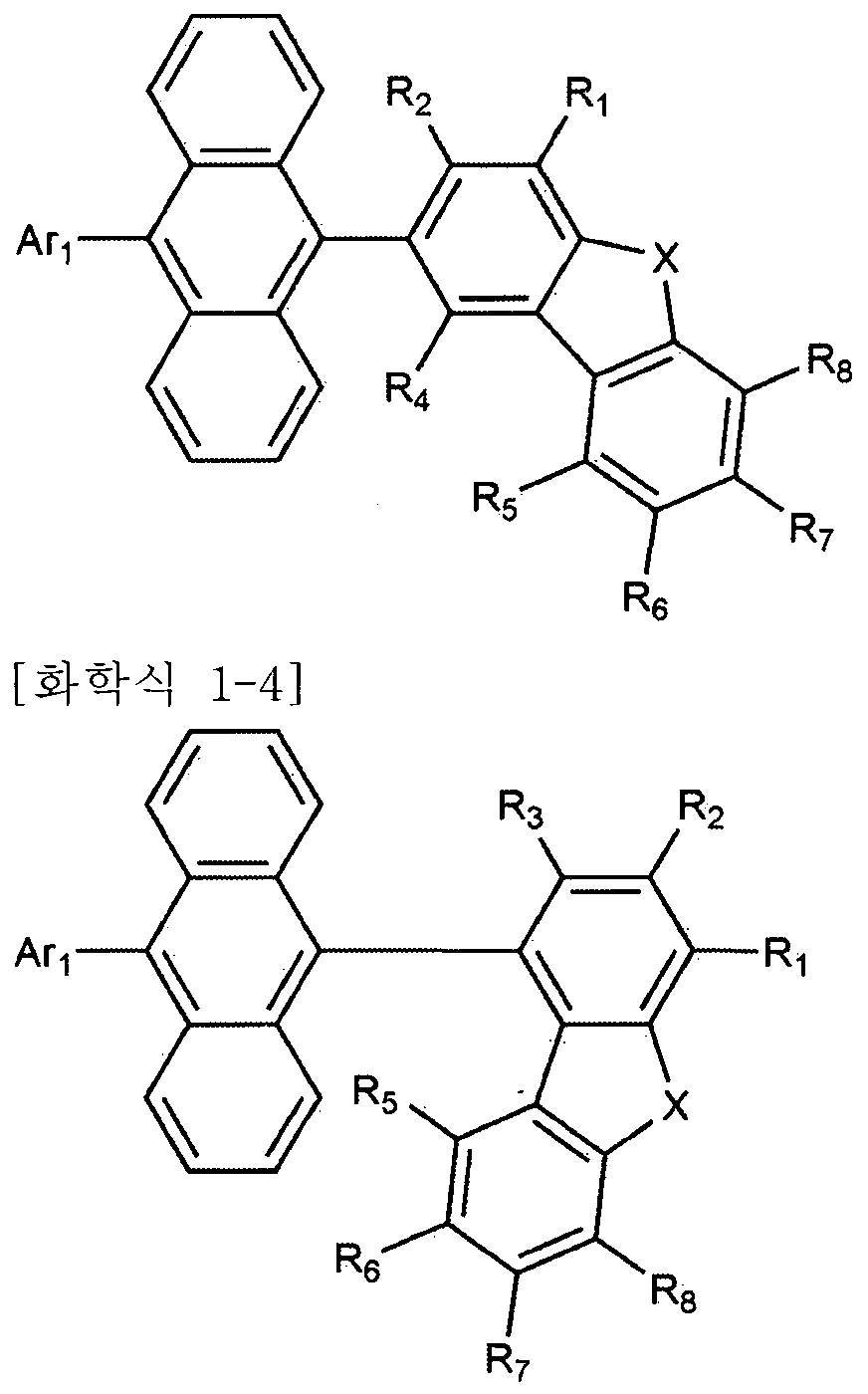
상기 화학식 1—1 내지 1-4에서, In Chemical Formula 1—1 to 1-4,
X 및 Ar^l 정의는 제 1항과 같고, X and Ar ^ l definition is the same as in claim 1,
상기 화학식 1-1에서. R 및 R3 내지 ¾은 각각 독립적으로 수소 또는 중수소이되. 및 내지 R8 중 적어도 하나는 중수소이고, In Chemical Formula 1-1. R and R 3 to ¾ are each independently hydrogen or deuterium. And at least one of R 8 is deuterium,
상기 화학식 1-2에서, R2 내지 ¾은 각각 독립적으로 수소 또는 중수소이되, ¾ 내지 ¾ 중 적어도 하나는 중수소이고, In Formula 1-2, R 2 to ¾ are each independently hydrogen or deuterium, at least one of ¾ to ¾ is deuterium,
상기 화학식 1-3에서, , 및 ¾ 내지 ¾은 각각 독립적으로 수소 또는 중수소이되, ¾, R2 및 R4 내지 ¾ 중 적어도 하나는 중수소이고, In Formula 1-3,, and ¾ to ¾ are each independently hydrogen or deuterium, at least one of ¾, R 2 and R 4 to ¾ is deuterium,
상기 화학식 1-4에서, 내지 R3 및 내지 R8은 각각 독립적으로 수소 또는 중수소이되, ^ 내지 ¾ 및 내지 ¾ 중 적어도 하나는 중수소이다. 바람직하게는, 상기 화학식 1-1의 및 내지 중에서, ¾; R4; R5; ; R7; R8; i 및 ; Re 및 ; Ri, 3 및 ; 5 내지 ; 또는 Ri 및 R3 내지 R8이 중수소이고, 나머지가 수소이다. 보다 바람직하게는, 상기 화학식 1-1의 및 R3 내지 R8 중에서, Rs 및 R4; R5 내지 ; 또는 ¾ 및 R3 내지 R8이 중수소이고, 나머지가 수소이다. 또한 바람직하게는, 상기 화학식 1-2의 내지 R8 중에서, R2; R3; R4; R5; R6; R7; R8; R2 및 ¾; R6 및 R8; R2 내지 ; 내지 ; 또는 ¾ 내지 ¾이 중수소이고, 나머지가 수소이다. 보다 바람직하게는, 상기 화학식 1-2의 내지 중에서, R2 내지 ¾; R5 내지 R8; 또는 R2 내지 R8이 중수소이고, 나머지가 수소이다. 또한 바람직하게는, 상기 화학식 1-3의 Rl R2 및 R4 내지 중에서,In Formula 1-4, to R 3 and R 8 are each independently hydrogen or deuterium, at least one of ^ to ¾ and to ¾ is deuterium. Preferably, in Formula 1-1 and above, ¾; R 4 ; R 5 ; ; R 7 ; R 8 ; i and; Re and; Ri, 3 and; 5 to; Or Ri and R 3 to R 8 are deuterium, with the remainder being hydrogen. More preferably, the In Formula 1-1 and R 3 to R 8 , Rs and R 4 ; R 5 to; Or ¾ and R 3 to R 8 are deuterium and the remainder is hydrogen. Also, preferably, in Formulas 1-2 to R 8 , R 2 ; R 3 ; R 4 ; R 5 ; R 6 ; R 7 ; R 8 ; R 2 and ¾; R 6 and R 8 ; R 2 to; To; Or ¾ to ¾ is deuterium and the remainder is hydrogen. More preferably, in Formula 1-2, R 2 to ¾; R 5 to R 8 ; Or R 2 to R 8 are deuterium, and the remainder are hydrogen. Also preferably, in Formulas 1-3 of R 1 R 2 and R 4 ,
Ri; ; ; ; R6; R7; ; 2 및 4; R6 및 ¾; Ri, R2 및 R4; R5 내지 또는 , 및 내지 ¾이 중수소이고, 나머지가 수소이다. 보다 바람직하게는, 상기 화학식 1-3의 , R2 및 R4 내지 중에서, Ri, R2 및 ; R5 내지 R8; 또는 , R2 및 R4 내지 ¾이 중수소이고, 나머지가 수소이다. 또한 바람직하게는-, 상기 화학식 1-4의 내지 및 R5 내지 R8 중에서, R,..; R2; ¾; R5; R6; 7; ; Ri 및 ¾:' ¾ 및 R8; Ri 내지 R3; R5 내지'。Ri; ; ; ; R 6 ; R 7 ; ; 2 and 4 ; R 6 and ¾; Ri, R 2 and R 4 ; R 5 to or, and to ¾ are deuterium and the remainder is hydrogen. More preferably, in Formulas 1-3, R 2 and R 4 to, Ri, R 2 and; R 5 to R 8 ; Or, R 2 and R 4 to ¾ are deuterium and the remainder is hydrogen. Also preferably, among Formulas 1-4 and R 5 to R 8 , R, ..; R 2 ; ¾; R 5 ; R 6 ; 7 ; ; Ri and ¾: ' ¾ and R 8 ; Ri to R 3 ; R 5 to ' .
; 또는 R! 내지 R3 및 R5 내지 R8 중수소이고, 나머지가 수소이다. 보다 바람직하게는. 상기 화학식 1-4의 내지 및 R5 내지 중에서, Ri 내지 R3; R5 내지 ; 또는 RL 내지 및 R5 내지 ¾ 중수소이고, 나머지가 수소이다ᅳ 바람직하게는, A 은 나프틸, 페닐나프틸, 페난트레닐, 또는 트리페닐레닐이다. 상기 화학식 1로 표시되는 화합물은, 하기 화합물로 구성되는 군으로부터 선택될 수 있다: ; Or R! To R 3 and R 5 to R 8 deuterium, with the remainder being hydrogen. More preferably. In Formulas 1-4 to and R 5 to, Ri to R 3 ; R 5 to; Or R L to and R 5 to ¾ deuterium, with the remainder being hydrogen. Preferably, A is naphthyl, phenylnaphthyl, phenanthrenyl, or triphenylenyl. The compound represented by Formula 1 may be selected from the group consisting of the following compounds:

10 10

11 11


상기 반응식 1에서, X '를 제외한 나머지 정의는 앞서 정의한 바와 같으며, X'는 할로겐이고, 보다 바람직하게는 브로로, 또는 클로로이다. 상기 반웅식 1은, 스즈키 커플링 반웅으로서, 팔라듬 촉매와 염기 존재하에 수행하는 것이 바람직하며, 스즈키 커플링 반웅을 위한 반응기는 당업계에 알려진 바에 따라 변경이 가능하다. 상기 제조 방법은 후술할- 제조예에서 보다 구체화될 수 있다. 또한, 본 발명은 상기 화학식 1로 표시되는 화합물을 포함하는 유기 발광 소자를 제공한다. 일례로.. 본 발명은 제 1 전극; 상기 제 1 전극과 대향하여 구비된 제 2 전극; 및 상기 게 1 전극과 상기 제 2 전극 사이에 구비된 1층 이상의 유기물 층을 포함하는 유기 발광 소자로서 상기 유기물 층 중 1층 이상은 상기 화학식 1로 표시되는 화합물을 포함하는, 유기 발광 소자를 제공한다. 본 발명의 유기 발광 소자의 유기물 층은 단층 구조로 이루어질 수도 있으나, 2층 이상의 유기물 충이 적층된 다충 구조로 이루어질 수 있다. 예컨대, 본 발명의 유기 발광 소자는 유기물 층으로서 정공 주입층, 정공 수송층, 발광층, 전자 수송충, 전자 주입층 등을 포함하는 구조를 가질 수 있다. 그러나 유기 발광 소자의 구조는 이에 한정되지 않고 더 적은 수의 유기층을 포함할 수 있다. 또한, 상기 유기물 층은 정공 주입층, 정공 수송층, 또는 정공 주입과 수송을 동시에 하는 층을 포함할 수 있고, 상기 정공 주입층, 정공 수송층, 또는 정공 주입과 수송을 동시에 하는 층은 상기 화학식 1로 표시되는 화합물을 포함할 수 있다. 또한, 상기 유기물 층은 발광충을 포함할 수 있고, 상기 발광층은 상기 화학식 1로 표시되는 화합물을 포함할 수 있다. 또한, 상기 유기물 층은 전자 수송층, 전자 주입층, 또는 전자 수송과 주입을 동시에 하는 층을 포함할 수 있고, 상기 전자 수송층, 전자 주입층, 또는 전자 수송과 주입을 동시에 하는 층은 상기 화학식 1로 표시되는 화합물을 포함할 수 있다. 또한, 본 발명에 따른 유기 발광 소자는 - , 기판 상에 양극, 1층 이상의 유기물 층 및 음극이 순차적으로 :적층된 구조 (normal type)의 유기 발광 소자일 수 있다. 또한, 본 발명에 따른 유기 발광 소자는 기판 상에 음극, 1층 이상의 유기물 층 및 양극이 순차적으로 적층된 역방향 구조 ( inverted type)의 유기 발광 소자일 수 있다. 예컨대, 본 발명의 일 실시예에 따른 유기 발광 소자의 구조는 도 1 및 2에 예시되^ 있다. 도 1은 기판 ( 1) , 양극 (2), 발광충 (3) , 음극 (4)으로 이루어진 유기 발광 소자의 예를 도시한 것이다. 이와 같은 구조에 있어서, 상기 화학식 1로 표시되는 화합물은 상기 발광층에 포함될 수 있다. 도 2는 기판 ( 1), 양극 (2), 정공 주입층 (5) , 정공 수송층 (6), 발광층 (7), 전자 수송층 (8) 및 음극 (4)로 이루어진 유기 발광 소자의 예를 도시한 것이다. 이와 같은 구조에 있어서, 상기 화학식 1로 표시되는 화합물은 상기 정공 주입층, 정공 수송층, 발광층 및 전자 수송층 중 1층 이상에 포함될 수 있다. 본 발명에 따른 유기 발광 소자는, 상기 유기물 층 중 1층 이상이 상기 화학식 1로 표시되는 화합물을 포함하는 것을 제외하고는 당 기술분야에 알려져 있는 재료와 방법으로 제조될 수 있다. 또한, 상기 유기 발광 소자가 복수개의 유기물 층을 포함하는 경우, 상기 유기물 층은 동일한 물질 또는 다른 물질로 형성될 수 있다. 예컨대. 본 발명에 따른 유기 발광 소자는 기판 상에 제 1 전극, 유기물 층 및 제 2 전극을 순차적으로 적층시켜 제조할 수 있다. 이때, 스퍼터링법 ( sput ter ing)이나 전자범 증발법 (e-beam evaporat ion)과 같은 PVD(phys i cal Vapor Depos i t ion)방법을 이용하여, 기판 상에 금속 또는 전도성을 가지는 금속 산화물 또는 이들의 합금을 증착시켜 양극을 형성하고, 그 위에 정공 주입층, 정공 수송층, 발광층 및 전자 수송충을 포함하는 유기물 층을 형성한 후, 그 위에 음극으로 사용할 수 있는 물질을 증착시켜 제조할 수 있다. 이와 같은 방법 외에도, 기판 상에 음극 물질부터 유기물 층, 양극 물질을 차례로 증착시켜 유기 발광 소자를 만들 수 있다. 또한. 상기 화학식 1로 표시되는 화합물은 유기 발광 소자의 제조시 진공 증착법 뿐만 아니라 용액 도포법에 의하여 유기물 충으로 형성될 수 있다. 여기서, 용액 도포법이라 함은 스핀 코팅, 딥코팅, 닥터 블레이딩. 잉크젯 프린팅, 스크린 프린팅, 스프레이법, 롤 코팅 등을 의미하지만, 이들만으로 한정되는 것은 아니다. 이와 같은 방법 외에도, 기판 상에 음극 물질로부터 유기물 충, 양극 물질을 차례로 증착시켜 유기 발광 소자를 제조할 수 있다 0V0 2003/012890) . 다만, 제조 방법이 이에 한정되는 것은 아니다. In Reaction Scheme 1, the remaining definitions except for X 'are as defined above, and X' is halogen, more preferably brolo or chloro. The reaction 1 is preferably performed in the presence of a paralysis catalyst and a base as a Suzuki coupling reaction, and a reactor for the Suzuki coupling reaction can be changed as known in the art. The production method may be more specified in the production examples to be described later. In addition, the present invention provides an organic light emitting device including the compound represented by Formula 1. In one example. The present invention comprises a first electrode; A second electrode provided to face the first electrode; And at least one organic material layer provided between the first electrode and the second electrode, wherein at least one of the organic material layers comprises a compound represented by Chemical Formula 1. do. The organic material layer of the organic light emitting device of the present invention may have a single layer structure, but may have a multi-layer structure in which two or more layers of organic material packs are stacked. For example, the organic light emitting device of the present invention may have a structure including a hole injection layer, a hole transport layer, a light emitting layer, an electron transport layer, an electron injection layer and the like as the organic layer. However, the structure of the organic light emitting device is not limited thereto and may include a smaller number of organic layers. In addition, the organic layer may include a hole injection layer, a hole transport layer, or a layer for simultaneously injecting and transporting holes, the hole injection layer, holes The transport layer, or the layer for simultaneously injecting and transporting a hole may include the compound represented by Chemical Formula 1. In addition, the organic layer may include a light emitting insect, and the light emitting layer may include a compound represented by Chemical Formula 1. The organic layer may include an electron transport layer, an electron injection layer, or a layer for simultaneously transporting and injecting electrons, and the electron transport layer, an electron injection layer, or a layer for simultaneously transporting and injecting electrons may be represented by Formula 1 above. It may include a compound represented. In addition, the organic light emitting device according to the present invention may be an organic light emitting device having a structure in which an anode, one or more organic material layers, and a cathode are sequentially stacked: on a substrate. In addition, the organic light emitting device according to the present invention may be an organic light emitting device of an inverted type in which a cathode, one or more organic material layers, and an anode are sequentially stacked on a substrate. For example, the structure of an organic light emitting device according to an embodiment of the present invention is illustrated in FIGS. 1 and 2. FIG. 1 shows an example of an organic light emitting element composed of a substrate 1, an anode 2, a light emitting insect 3, and a cathode 4. In such a structure, the compound represented by Formula 1 may be included in the light emitting layer. FIG. 2 shows an example of an organic light emitting element consisting of a substrate 1, an anode 2, a hole injection layer 5, a hole transport layer 6, a light emitting layer 7, an electron transport layer 8 and a cathode 4 It is. In such a structure, the compound represented by Formula 1 may be included in one or more layers of the hole injection layer, the hole transport layer, the light emitting layer and the electron transport layer. The organic light emitting device according to the present invention, except that at least one layer of the organic material layer comprises a compound represented by the formula (1) It may be made of materials and methods known in the art. In addition, when the organic light emitting device includes a plurality of organic material layers, the organic material layers may be formed of the same material or different materials. for example. The organic light emitting device according to the present invention may be manufactured by sequentially stacking a first electrode, an organic material layer, and a second electrode on a substrate. At this time, a metal oxide or a metal oxide having a conductivity or a metal on a substrate by using a physical vapor deposition deposition (PVD) method such as sputtering or e-beam evaporat ion An alloy is deposited to form an anode, and an organic material layer including a hole injection layer, a hole transport layer, a light emitting layer, and an electron transport insect may be formed thereon, and then, a material usable as a cathode may be deposited thereon. In addition to the above method, an organic light emitting device may be manufactured by sequentially depositing a cathode material, an organic material layer, and an anode material on a substrate. Also. The compound represented by Chemical Formula 1 may be formed into an organic material charge by a solution coating method as well as a vacuum deposition method in manufacturing an organic light emitting device. Here, the solution coating method is spin coating, dip coating, doctor blading. Inkjet printing, screen printing, spraying, roll coating and the like, but is not limited to these. In addition to the above method, an organic light emitting device may be manufactured by sequentially depositing an organic material charge and an anode material from a cathode material on a substrate 0V0 2003/012890). However, the manufacturing method is not limited thereto.
、 、
일례로, 상기 제 1 전극은 양극이고, 상기 제 2 전극은 음극이거나, 또는 상기 게 1 전극은 음극이고, 상기 제 2 전극은 양극이다. 상기 양극 물질로는 통상 유기물 층으로 정공 주입이 원활할 수 있도록 일함수가 큰 물질이 바람직하다. 상기 양극 물질의 구체적인 예로는 바나듐, 크롬, 구리, 아연, 금과 같은 금속 또는 이들의 합금; 아연 산화물, 인듐 산화물, 인듐주석 산화물 ( IT0) , 인듐아연 산화물 ( IZ0)과 같은 금속 산화물; Ζη0:Α1 또는 SN02 : Sb와 같은 금속과 산화물의 조합; 폴리 (3- 메틸티오펜), 폴리 [3,4- (에틸렌— 1 , 2-디옥시)티오펜 KPED0T) , 폴리피를 및 폴리아닐린과 같은 전도성 고분자 등이 있으나, 이들에만 한정되는 것은 아니다. 상기 음극 물질로는 통상 유기물 층으로 전자 주입이 용이하도록 일함수가 작은 물질인 것이 바람직하다. 상기 음극 물질의 구체적인 예로는 마그네슘, 칼슘, 나트륨, 칼륨, 티타늄, 인듐, 이트륨. 리튬, 가돌리늄, 알루미늄, 은, 주석 및 납과 같은 금속 또는 이들의 합금; LiF/Al 또는 U¾/A1과 같은 다층 구조 물질 등이 있으나, 이들에만 한정되는 것은 아니다. 상기 정공 주입층은 전극으로부터 정공을 주입하는 층으로., 정공 주입 물질로는 정공을 수송하는 능력을 가져 양극에서의 정공 주입 효과, 발광 또는 발광 재료에 대하여 우수한 정공. 주입 효과를 갖고, 발광충에서 생성된 여기자의 전자 주입층 또는 전지- 주입 재료에의 이동을 방지하며, 또한, 박막 형성 능력이 우수한 화합물이 바람직하다. 정공 주입 물질의 H0M0(highest occupi ed molecul ar orbi tal )가 양극 물질의 일함수와 주변 유기물 층의 HOMO 사이인 것이 바람직하다. 정공 주입 물질의 구체적인 예로는 금속 포피린 (porphyr in) , 올리고티오펜, 아릴아민 계열의 유기물, 핵사니트릴핵사아자트리페닐렌 ■ 계열의 유기물, 퀴나크리돈 (qu inacr i done)계열의 유기물, 페릴렌 (perylene) 계열의 유기물, 안트라퀴논 및 폴리아닐린과 폴리티오펜 계열의 전도성 고분자 등이 있으나, 이들에만 한정 되는 것은 아니다. 상기 정공 수송층은 정공 주입층으로부터 정공을 수취하여 발광층까지 정공을 수송하는 충으로, 정공 수송 물질로 양극이나 정공 주입층으로부터 정공을 수송 받아 발광층으로 옮겨줄 수 있는 물질로 정공에 대한 이동성이 큰 물질이 적합하다. 구체적인 예로는 아릴아민 계열의 유기물, 전도성 고분자, 및 공액 부분과 비공액 부분이 함께 있는 블록 공중합체 등이 있으나, 이들에만 한정되는 것은 아니다. 상기 발광 물질로는 정공 수송층과 전자 수송층으로부터 정공과 전자를 각각 수송 받아 결합시킴으로써 가시광선 영역의 빛을 낼 수 있는 물질로서, 형광이나 인광에 대한 양자 효율이 좋은 물질이 바람직하다. 구체적인 예로 8—히드록시—퀴놀린 알루미늄 착물 (Alq3) ; 카르바졸 계열 화합물; 이량체화 스티릴 (dimer i zed styryl ) 화합물; BAlq ; 10- 히드록시벤조 퀴놀린—금속 화합물; 벤족사졸, 벤즈티아졸 및 벤즈이미다졸 계열의 화합물 ; 폴리 (P-페닐렌비닐렌) (PPV) 계열의 고분자; 스피로 ( spi ro) 화합물; 폴리플후오렌, 루브렌 등이 있으나, 이들에만 한정되는 것은 아니다ᅳ 상기 발광층은 호스트 재료 및 도편트 재료를 포함할 수 있다. 호스트 재료는 축합 방향족환 유도체 또는 헤테로환 함유 화합물 등이 있다. 구체적으로. 축합 방향족환 유도체로는 안트라센 유도체 ,, 피렌 유도체, 나프탈렌 유도체, 펜타센 유도체, 페난트렌 화합물. 풀루오란텐 화합물 등이 있고. 헤테로환 함유 화합물로는 카바졸 유도체, 디벤조퓨란 유도체, 래더형 퓨란 화합물, 피리미딘 유도체 등이 있으나, 이에 한정되지 않는다. 구체적으로, 상기 발광층은 상기 호스트 재료로서 상기 화학식 1로 표시되는 화합물을 포함할 수 있다. 특히, 청색 발광층의 호스트 재료로서 상기 화학식 1로 표시되는 화합물을 사용하여 우수한 효율의 유기 발광 소자를 제공할 수 있다. 도편트 재료로는 방향족 아민 유도체, 스트릴아민 화합물, 붕소 착처 1, 플루오란텐 화합물, 금속 착체 등이 있다. 구체적으로 방향족 아민 유도체로는 치환 또는 비치환된 아릴아미노기를 갖는 축합 방향족환 유도체로서, 아릴아미노기를 갖는 피렌, 안트라센, 크리센, 페리플란텐 등이 있으며, 스티릴아민 화합물로는 치환 또는 비치환된 아릴아민에 적어도 1개의 아릴비닐기가 치환되어 있는 화합물로, 아릴기, 실릴기. 알킬기. 시클로알킬기 및 아릴아미노기로 이루어진 군에서 1 또는 2 이상 선택되는 치환기가 치환 또는 비치환된다. 구체적으로 스티릴아민, 스티릴디아민ᅳ 스티릴트리아민, 스티릴테트라아민 등이 있으나, 이에 한정되지 않는다. 또한, 금속 착체로는 이리듭 착체ᅳ 백^ 착체 등이 있으나, 이에 한정되지 않는다. 상기 전자 수송층은 전자 주입충으로부터 전자를 수취하여 발광충까지 전자를 수송하는 층으로, 전자 수송 물질로는 음극으로부터 전자를 잘 주입 받아 발광층으로 옮겨줄 수 있는 물질로서, 전자에 대한 이동성이 큰 물질이 적합하다. 구체적인 예로는 8-히드록시퀴놀린의 A1 착물; Al q3를 포함한 착물; 유기 라디칼 화합물; 히드록시플라본 -금속 착물 등이 있으나, 이들에만 한정되는 것은 아니다. 전자 수송층은 종래기술에 따라 사용된 바와 같이 임의의 원하는 캐소드 물질과 함께 사용할 수 있다. 특히, 적절한 캐소드 물질의 예는 낮은 일함수를 가지고 알루미늄층 또는 실버충이 뒤따르는 통상적인 물질이다。 구체적으로 .세슘, 바륨, 칼슘, 이테르븀 및 사마륨이고, 각 경우 알루미늄 충 또는 실버층이 뒤따른다. 상기 전자 주입층은 전극으로부터 전자를 주입하는 층으로, 전자를 수송하는 능력을 갖고, 음극으로부터의 전자 주입 효과, 발광층 또는 발광 재료에 대하여 우수한 전자 주입 효과를 가지며, 발광층에서 생성된 여기자의 정공 주입층으로의 이동을 방지하고, 또한, 박막형성능력이 우수한 화합물이 바람직하다. 구체적으로는 플루오레논, 안트라퀴노다이메탄, 다이페노퀴논. 티오피란 다이옥사이드, 옥사졸, 옥사다이아졸. 트리아졸, 이미다졸, 페릴렌테트라카복실산, 프레오레닐리덴 메탄, 안트론 등과 그들의 유도체, 금속 착체 화합물 및 질소 함유 5원환 유도체 등이 있으나, 이에 한정되지 않는다. 상기 금속 착체 화합물로서는 8—하이드록시퀴놀리나토 리튬, 비스 (8- 하이드록시퀴놀리나토)아연, 비스 (8-하이드록시퀴놀리나토)구리, 비스 (8- 하이드록시퀴놀리나토)망간, 트리스 (8-하이드록시퀴놀리나토)알루미늄, 트리스 (2-메틸 -8-하이드록시퀴놀리나토)알루미늄, 트리스 (8- 하이드록시퀴놀리나토)갈륨, 비스 ( 10-하이드록시벤조 [h]퀴놀리나토)베릴륨, 비스( 10-하이드록시벤조 [h]퀴놀리나토)아연 , 비스 (2-메틸 -8- 퀴놀리나토)클로로갈륨, 비스 (2—메틸 -8-퀴놀리나토) ( 0-크레졸라토)갈륨, 비스 ( 2-메틸 -8-퀴놀리나토 ) ( 1-나프를라토)알루미늄, 비스 ( 2-메틸 -8- 퀴놀리나토) (2-나프를라토)갈륨 등이 있으나, 이에 한정되지 않는다. 본 발명에 따른 유기 발광 소자는 사용되는 재료에 따라 전면 발광형 , 후면 발광형 또는 양면 발광형일 수 있다. 또한, 상기 화학식 1로 표시되는 화합물은 유기 발광 소자 외에도 유기 태양 전지 또는 유기 트랜지스터에 포함될 수 있다. 상기 화학식 1로 표시되는 화합물 및 이를 포함하는 유기 발광 소자의 제조는 이하 실시예에서 구체적으로 설명한다. 그러나 하기 실시예는 본 발명을 예시하기 위한 것이며, 본 발명의 범위가 이들에 의하여 한정되는 것은 아니다. In one example, the first electrode is an anode, the second electrode is a cathode, or the first electrode is a cathode, the second electrode is an anode. As the anode material, a material having a large work function is generally preferred to facilitate hole injection into the organic material layer. Specific examples of the positive electrode material Metals such as vanadium, chromium, copper, zinc and gold or alloys thereof; Metal oxides such as zinc oxide, indium oxide, indium tin oxide (IT0), indium zinc oxide (IZ0); Η η 0: A1 or SN0 2 : a combination of a metal and an oxide such as Sb; Conductive polymers such as poly (3-methylthiophene), poly [3,4- (ethylene-1,2-dioxy) thiophene KPED0T), polypyri and polyaniline, and the like, but are not limited thereto. It is preferable that the cathode material is a material having a small work function to facilitate electron injection into the organic material layer. Specific examples of the negative electrode material include magnesium, calcium, sodium, potassium, titanium, indium, and yttrium. Metals such as lithium, gadolinium, aluminum, silver, tin and lead or alloys thereof; Multilayer structure materials such as LiF / Al or U¾ / A1, and the like, but are not limited thereto. The hole injection layer is a layer for injecting holes from the electrode. The hole injection material has a capability of transporting holes, and has excellent hole injection effects at the anode, and excellent holes for light emitting or light emitting materials. The compound which has an injection effect, prevents the movement of the excitons which generate | occur | produced in the luminescent charge to an electron injection layer or a battery-injection material, and is excellent in thin film formation ability is preferable. It is preferred that the highest occupied molecul ar orbital (H0M0) of the hole injection material be between the work function of the anode material and the HOMO of the surrounding organic layer. Specific examples of the hole injecting material is a metal porphyrin (porphyr in), oligothiophene, arylamine series of organic matter, hex nitrile hex-aza triphenylene ■ organic substance in the series, quinacridone (qu inacr i done) organic substance in the series, Fe Perylene organic materials, anthraquinone and polyaniline and polythiophene-based conductive polymers, but are not limited thereto. The hole transport layer is a material that receives holes from the hole injection layer and transports holes to the light emitting layer. The hole transport layer is a material that can transport holes from an anode or a hole injection layer to a light emitting layer as a hole transport material. Materials with high mobility for holes are suitable. Specific examples include an arylamine-based organic material, a conductive polymer, and a block copolymer having a conjugated portion and a non-conjugated portion, but are not limited thereto. The light emitting material is a material capable of emitting light in the visible region by transporting and combining holes and electrons from the hole transport layer and the electron transport layer, respectively, and a material having good quantum efficiency with respect to fluorescence or phosphorescence is preferable. Specific examples include 8—hydroxy-quinoline aluminum complex (Alq 3 ); Carbazole series compounds; Dimer i zed styryl compounds; BAlq; 10-hydroxybenzoquinoline—metal compound; Benzoxazole, benzthiazole and benzimidazole series compounds; Polymers of the poly (P-phenylenevinylene) (PPV) family; Spi ro compounds; Polyfluorene, rubrene, and the like, but are not limited thereto. The light emitting layer may include a host material and a dopant material. The host material is a condensed aromatic ring derivative or a heterocyclic containing compound. Specifically. Condensed aromatic ring derivatives include anthracene derivatives, pyrene derivatives, naphthalene derivatives, pentacene derivatives, and phenanthrene compounds. And pulluloranthene compounds. Heterocyclic containing compounds include, but are not limited to carbazole derivatives, dibenzofuran derivatives, ladder type furan compounds, pyrimidine derivatives, and the like. Specifically, the light emitting layer may include a compound represented by Formula 1 as the host material. In particular, it is possible to provide an organic light emitting device having excellent efficiency by using the compound represented by Formula 1 as a host material of the blue light emitting layer. The dopant materials include aromatic amine derivatives, styrylamine compounds, boron complex 1, fluoranthene compounds, metal complexes, and the like. Specifically, the aromatic amine derivative is a condensed aromatic ring derivative having a substituted or unsubstituted arylamino group, and includes pyrene, anthracene, chrysene and periplanthene having an arylamino group. The styrylamine compound is a compound in which at least one arylvinyl group is substituted with a substituted or unsubstituted arylamine, and an aryl group and a silyl group. Alkyl group. One or two or more substituents selected from the group consisting of a cycloalkyl group and an arylamino group are substituted or unsubstituted. Specifically, styryl amine, styryl diamine styryl triamine, styryl tetraamine and the like, but is not limited thereto. In addition, the metal complex includes a lychee complex, a back complex, and the like, but is not limited thereto. The electron transport layer is a layer that receives electrons from the electron injection charge and transports the electrons to the light emitting charge, and the electron transport material is a material that can inject electrons well from the cathode and transfer them to the light emitting layer. Suitable. Specific examples include Al complexes of 8-hydroxyquinoline, complexes including Al q 3 ; Organic radical compounds; Hydroxyflavone-metal complexes and the like, but are not limited thereto. The electron transport layer can be used with any desired cathode material as used in accordance with the prior art. In particular, examples of suitable cathode materials are conventional materials having a low work function followed by an aluminum layer or silver worm. Specifically, cesium, barium, calcium, ytterbium and samarium, in each case followed by an aluminum worm or silver layer. The electron injection layer is a layer for injecting electrons from an electrode, has a capability of transporting electrons, has an electron injection effect from the cathode, excellent electron injection effect to the light emitting layer or the light emitting material, and hole injection of excitons generated in the light emitting layer The compound which prevents the movement to a layer and is excellent in thin film formation ability is preferable. Specifically, fluorenone, anthraquinodimethane, diphenoquinone. Thiopyran dioxide, oxazole, oxadiazole. Triazole, imidazole, perylene tetracarboxylic acid, preorenylidene methane, anthrone and the like, derivatives thereof, metal complex compounds and nitrogen-containing five-membered ring derivatives, and the like, but are not limited thereto. As said metal complex compound, 8-hydroxyquinolinato lithium, bis (8- Hydroxyquinolinato zinc, bis (8-hydroxyquinolinato) copper, bis (8-hydroxyquinolinato) manganese, tris (8-hydroxyquinolinato) aluminum, tris (2-methyl- 8-hydroxyquinolinato) aluminum, tris (8-hydroxyquinolinato) gallium, bis (10-hydroxybenzo [h] quinolinato) beryllium, bis (10-hydroxybenzo [h] quinolina Earth, zinc, bis (2-methyl-8-quinolinato) chlorogallium, bis (2-methyl-8-quinolinato) (0-crezolato) gallium, bis (2-methyl-8-quinolinato) ) (1-naphtholato) aluminum, bis (2-methyl-8-quinolinato) (2-naphtholato) gallium, and the like. The organic light emitting device according to the present invention may be a top emission type, a bottom emission type or a double-sided emission type depending on the material used. In addition, the compound represented by Formula 1 may be included in an organic solar cell or an organic transistor in addition to the organic light emitting device. Preparation of the compound represented by Chemical Formula 1 and an organic light emitting device including the same will be described in detail in the following Examples. However, the following examples are intended to illustrate the present invention, and the scope of the present invention is not limited thereto.
[제조예] [Production example]
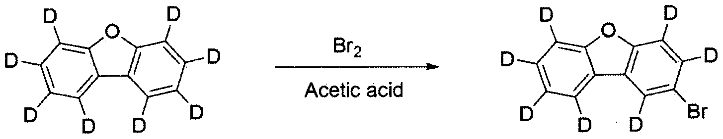
2구 플라스크에 디벤조 [b , d]퓨란 -(18(50.0 g , 283.7 麵 ol )을 아세트산 (500 ml )에 아르곤 분위기 조건 하에서 가열하여 녹였다. 여기에 브로민 ( 17 ml , 340.4 隱 ol )을 천천히 적가한 후, 상온으로 식히면서 20시간 동안 교반하였다. 반웅이 종료되면 생성된 고체를 여과하여. 아세트산과 물로 씻어주고 메탄올을 이용하여 재결정하여 중간체 A를 수득하였다 (30.3 g. 수율 42%. MS: [M+H]+= 254). In a two-necked flask, dibenzo [b, d] furan- (18 (50.0 g, 283.7 麵 ol) was dissolved in acetic acid (500 ml) by heating under argon atmosphere. Bromine (17 ml, 340.4 隱 ol) After slowly adding dropwise, the mixture was stirred for 20 hours while cooling to room temperature. Washed with water and recrystallized with methanol to obtain intermediate A (30.3 g. Yield 42%. MS: [M + H] + = 254).

B B
건조된 3구 플라스크에 디벤조 [b,d]퓨란 -d8(50.0 g, 283.7 隱01)을 질소 분위기 하에서 THF(500 ml)에 녹인 후, -78°C에서 교반하면서 1.6M n- 부틸리튬 (186 ml, 297.9 mniol)을 천천히 적가하였다. 적가가 완료되면 - 78°C를 유지하며 1시간 더 교반하였다. 그 후, 트리메틸 보레이트 (38.3 g, 368.8 隱 ol)를 천천히 적가한 후, 상온으로 올려서 1시간 교반하였다-. 반응이 종료되면 2N HC1 수용액 (200 ml)을 상온에서 적가한 후 30분 동안 교반하였다. 반응액을 분액 깔대기에 옮기고 물과 에틸 아세테이트를 이용하여 유기층을 추출하여 감압 농축한 후, CH2C12와 핵산으로 재결정하여 중간체 B* 수득하였다 (29.8. g., 수율 48%, MS: [M+H]+= 219). 제조예 3: 중간체 C의 제조 Dibenzo [b, d] furan-d8 (50.0 g, 283.7 隱0 1) was dissolved in THF (500 ml) under a nitrogen atmosphere in a dried three-necked flask and 1.6M n-butyl with stirring at -78 ° C. Lithium (186 ml, 297.9 mniol) was slowly added dropwise. When the dropwise addition was completed, the mixture was stirred for 1 hour while maintaining at -78 ° C. Thereafter, trimethyl borate (38.3 g, 368.8 Pa ol) was slowly added dropwise, and then raised to room temperature and stirred for 1 hour. After the reaction was completed, 2N HC1 aqueous solution (200 ml) was added dropwise at room temperature, followed by stirring for 30 minutes. Transfer the reaction mixture to a separatory funnel and then the organic layer was extracted using water and ethyl acetate, and concentrated under reduced pressure, CH 2 C1 was recrystallized in two nucleic acid intermediates B * obtained (29.8 g, yield 48%, MS:.. [ M + H] + = 219). Preparation Example 3 Preparation of Intermediate C

C-1 C-1
건조된 3구 플라스크에 1,3-디메톡시벤젠—2, 4, 5,6ᅳ (14(50.0 g, 351.6 麵 ol)을 질소 분위기 하에서 THF(500 ml)에 녹인 후, -10°C에서 교반하면서 1.6M n-부틸리튬 (231 ml, 369.2 画 ol)을 천천히 적가하였다. 적가가 완료되면 동일 은도에서 4시간 더 교반한 후, -78°C로 온도를 내리고 트리메틸 보레이트 (47.5 g, 457.1 mniol)를 천천히 적가한 후, 상온으로 을려서 밤새 교반하였다. 반웅이 종료되면 2N HC1 수용액을 적가하여 산성화한 후 30분 동안 교반하였다. 반웅액을 분액 깔대기에 옮기고 물과 에틸 아세테이트를 이용하여 유기층을 추출하여 감압 농축한 후, 핵산으로 재결정하여 중간체 C-1을 수득하였다 (45.5 g, 수율 70%, MS: [M+H]+= 185). 1,3-dimethoxybenzene—2, 4, 5,6 ᅳ (14 (50.0 g, 351.6 麵 ol)) was dissolved in THF (500 ml) under a nitrogen atmosphere in a dried three-neck flask at -10 ° C. 1.6 M n-butyllithium (231 ml, 369.2 画 ol) was slowly added dropwise with stirring, after which the addition was completed, the mixture was stirred for 4 more hours at the same degree, and then cooled to -78 ° C and trimethyl borate (47.5 g, 457.1 mniol) was slowly added dropwise, followed by stirring overnight at room temperature. After reaction was completed, 2N HC1 aqueous solution was added dropwise. After acidification it was stirred for 30 minutes. The reaction solution was transferred to a separatory funnel, the organic layer was extracted with water and ethyl acetate, concentrated under reduced pressure, and recrystallized with nucleic acid to obtain Intermediate C-1 (45.5 g, yield 70%, MS: [M + H] + = 185).
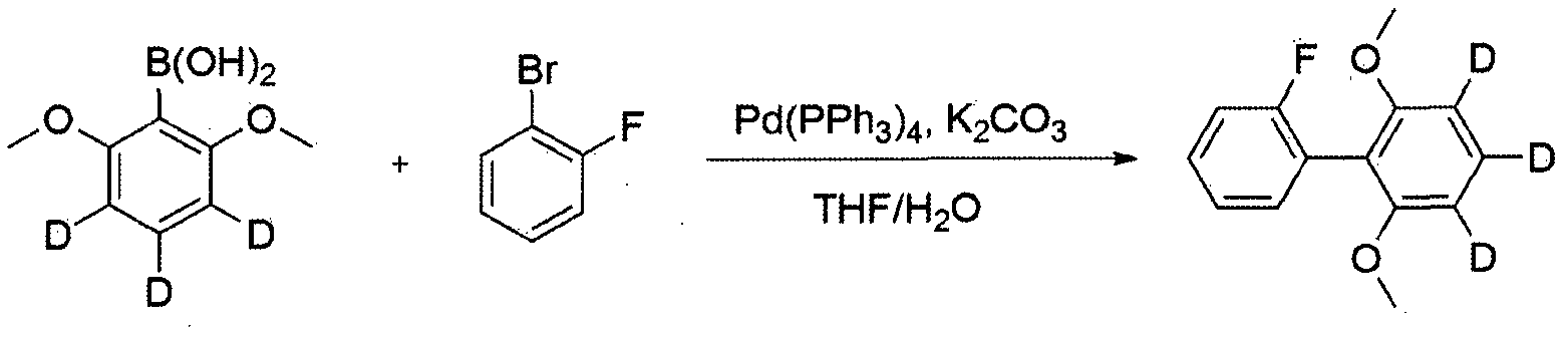
3구 플라스크에 중간체 01(45.0 g, 243.2 mmol), 1-브로모 -2- 플루오로벤젠 (46.8 g. 267.6 画 ol)을 THF(675 ml)에 녹이고 K2C03(134.5 g, 973.0 mmol)을 물 (338 ml)에 녹여 넣었다. 여기에 Pd(PPh3)4(H.2 g, 9.7 mmol)를 넣고, 아르곤 분위기 환류 조건 하에서 8시간 동안 교반하였다. 반응이 종료되면 상온으로 넁각한 후, 반응액을 분액 깔대기에 옮기고, 물과 에틸 아세테이트로 추출하였다ᅳ 추출액을 MgS04로 건조 후, 여과 및 농축한 후, 시료를 실리카 겔 컬럼 크로마토그래피로 정제하여 중간체 0 2-1- 수득하였다 (44.6 g, 수율 78%. MS: [M+H]+- 235). Intermediate 01 (45.0 g, 243.2 mmol), 1-bromo-2-fluorobenzene (46.8 g. 267.6 μl ol) were dissolved in THF (675 ml) in a three neck flask and K 2 CO 3 (134.5 g, 973.0 mmol) ) Was dissolved in water (338 ml). Pd (PPh 3 ) 4 (H.2 g, 9.7 mmol) was added thereto, and the mixture was stirred for 8 hours under reflux conditions under argon. After the reaction was completed, the mixture was cooled to room temperature, the reaction solution was transferred to a separatory funnel, extracted with water and ethyl acetate. The extract was dried over MgS0 4 , filtered and concentrated, and the sample was purified by silica gel column chromatography. Intermediate 0 2-1- was obtained (44.6 g, yield 78%. MS: [M + H] + -235).
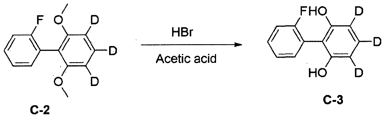
3구 플라스크에 중간체 02(40.0 g, 276.3 隱 ol)와 아세트산 (240 ml) HBr(160 ml)를 넣고 환류 조건 하에서 밤새 교반하였다. 반웅이 종료되면 상온으로 넁각한 후 반웅액에 물 (500 ml)을 조금씩 적가하였다. 그 후 반웅액을 분액 깔대기에 옮기고, 물과 에틸 아세테이트로 유기층을 추출하였다. 추출액을 MgS04로 건조하고 여과 및 농축한 후, 시료를 실리카 겔 컬럼 크로마토그래피로 정제하여 중간체 C-3을 수득하였다 (32.4 g, 수율 92%, MS: [M+H]+= 207).

3구 플라스크에 중간체 03(30.0 g, 144.8 mmol), 2C03(40.0 g, 289.5 mmol), NMP(400 nil)를 넣고 120°C에서 밤새 교반하였다. 반응이 종료되면 상은으로 넁각한 후 반응액에 물 (500 ml)을 조금씩 적가하였다ᅳ 그 후 반응액을 분액 깔대기에 옮기고, 물과 에틸 아세테이트로 유기층을 추출하였다. 추출액을 MgS04로 건조하고, 여과 및 농축한 후, 시료를 실리카 겔 컬럼 크로마토그래피로 정제하여 중간체 C-4를 수득하였다 (23.0 g, 수율 85%, MS: [M+H]+= 187). Intermediate 03 (30.0 g, 144.8 mmol), 2 CO 3 (40.0 g, 289.5 mmol) and NMP (400 nil) were added to a three neck flask and stirred at 120 ° C overnight. After the reaction was completed, the reaction solution was stirred with silver, and water (500 ml) was added dropwise to the reaction solution. After that, the reaction solution was transferred to a separatory funnel, and the organic layer was extracted with water and ethyl acetate. The extract was dried over MgSO 4 , filtered and concentrated, and the sample was purified by silica gel column chromatography to give intermediate C-4 (23.0 g, yield 85%, MS: [M + H] + = 187). .

3구 플라스크에 중간체 C-4(20.으 g,. · 106.8 mmol)를 아세토나이트릴 (560 ml)에 녹인 후, 트리에틸아민 (24 ml, 170.9 隱 ol), 퍼플루오로 -1-부탄술포닐 플루오라이드 (29 ml, 160.2 mmol)을 넣고 상온에서 밤새 교반하였다. 반웅이 종료되면 에틸 아세테이트로 묽히고 분액 깔대기에 옮겨 0.5M 소디움 바이설페이트 수용액을 이용하여 씻어준 후, 유기층을 추출하였다. 추출액을 MgS04로 건조하고, 여과 및 농축한 후, 시료를 실리카 겔 컬럼 크로마토그래피로 정제하여 중간체 C를 수득하였다 (36.1 g, 수율 72%, MS: [M+H]+= 469). 제조예 4: 중간체 D의 제조 Intermediate C-4 (20 g, 106.8 mmol) was dissolved in acetonitrile (560 ml) in a three-necked flask, and then triethylamine (24 ml, 170.9 隱 ol), perfluoro-1-butane Sulfonyl fluoride (29 ml, 160.2 mmol) was added and stirred at room temperature overnight. When the reaction was completed, the mixture was diluted with ethyl acetate, transferred to a separatory funnel, washed with an aqueous 0.5 M sodium bisulfate solution, and the organic layer was extracted. The extract was dried over MgSO 4 , filtered and concentrated, and the sample was purified by silica gel column chromatography to give Intermediate C (36.1 g, yield 72%, MS: [M + H] + = 469). Preparation Example 4 Preparation of Intermediate D
단계 1) 중간체 D-1의 제조 Step 1) Preparation of Intermediate D-1
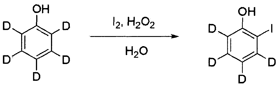
D-1 D-1
2구 플라스크에 과산화수소 30 wt% 수용액 (60 ml, 529.6 mmol)을 넣고 여기에 펜— d5-올 (50.0 g, 504.3 隱 ol)과 아이오딘 (64.8 g, 252.2 mmol)을 증류수 (500 ml)에 녹여 넣은 후. 50°C에서 24시간 동안 교반하였다. 반웅이 종료되면 소디움 티오설페이트 수용액을 넣어 교반한 후, 반응액을 분액 깔대기에 옮겨 물과 에틸 아세테이트로 유기층을 추출하였다. 추출액을 MgS04로 건조하고, 여과 및 농축힌 후, 시료를 실리카 겔 컬럼 크로마토그래피로 정제하여 중간체 D-1을 수득하였다 (54.2 g, 수율 48%, MS: [M+H]+= 224). Put a 30 wt% aqueous solution of hydrogen peroxide (60 ml, 529.6 mmol) in a two-necked flask and add pen-d5-ol (50.0 g, 504.3 μl) and iodine (64.8 g, 252.2 mmol) to distilled water (500 ml). After melting. Stir at 50 ° C for 24 h. After the reaction was completed, an aqueous solution of sodium thiosulfate was added thereto, followed by stirring. The reaction solution was transferred to a separating funnel, and the organic layer was extracted with water and ethyl acetate. The extract was dried over MgSO 4 , filtered and concentrated, and the sample was purified by silica gel column chromatography to give intermediate D-1 (54.2 g, yield 48%, MS: [M + H] + = 224). .

D-1 D-2 D-1 D-2
2구 플라스크에 중간체 D— 1(50.0 g, 223.2 mmol), NBS(41.7 g, 234.3 mmol), DMF(1000 mL)를 넣고, 아르곤 분위기 하에서 상온에서 8시간 동안 교반하였다. 반웅 종료 후, 반웅액을 분액 깔대기에 옮기고, 물과 에틸 아세테이트로 유기층을 추출하였다. 추출액을 MgS04로 건조하고, 여과 및 농축한 후, 시료를 실리카 겔 컬럼 크로마토그래피로 정제하여 중간체 D- 2를 수득하였다 (57.3 g, 수율 85%, MS: [M'+H]+= 302). 단계 3) 증간체 D— 3의 제조

3구. 플라스크에 중간체 D-2(55.0 g, 182.2 瞧 ol), (2- 플루오로페닐)보론산 (28.0 g, 200.4 隱 ol)을 THF(825 ml)에 녹이고 2C03(100.7 g, 728.7 画 ol)을 물 (413 ml)에 녹여 넣었다. 여기에 Pd(PPh3)4(8.4 g, 7.3隱 ol)를 넣고, 아르곤 분위기 환류 조건 하에서 8시간 동안 교반하였다. 반웅이 종료되면 상온으로 넁각한 후, 반응액을 분액 깔대기에 옮기고, 물과 에틸 아세테이트로 추출하였다. 추출액을 MgS04로 건조 후, 여과 및 농축한 후, 시료를 실리카 겔 컬럼 ΞΪ로마토그래피로 정제하여 중간체 D-3를 수득하였다 (36.9 g, 수율 75%. MS: [M+H]+= 270). 3 ball. Dissolve intermediate D-2 (55.0 g, 182.2 瞧 ol), (2-fluorophenyl) boronic acid (28.0 g, 200.4 隱 ol) in THF (825 ml) in a flask and add 2C0 3 (100.7 g, 728.7 画 ol) Was dissolved in water (413 ml). Pd (PPh 3 ) 4 (8.4 g, 7.3 Pa) was added thereto, and the mixture was stirred for 8 hours under reflux conditions under argon. When the reaction was completed, the reaction solution was cooled to room temperature, the reaction solution was transferred to a separatory funnel, and extracted with water and ethyl acetate. The extract was dried over MgSO 4 , filtered and concentrated, and the sample was purified by silica gel column chromatography to give Intermediate D-3 (36.9 g, yield 75%. MS: [M + H] + = 270).

D-3 D D-3 D
3구 플라스크에 중간체 I)-3(36.0 g, 133.3 隱 ol), K2C03(36.8 g, 266.5 mmol). NMP(470 ml)를 넣고 120°C에서 밤새 교반하였다. 반응이 종료되면 상은으로 넁각한 후 반응액에 물 (500 ml)을 조금씩 적가하였다. 그 후 반응액을 분액 깔대기에 옮기고ᅳ 물과 에틸 아세테이트로 유기층을 추출하였다. 추출액을 MgS04로 건조하고, 여과 및 농축한 후, 시료를 실리카 겔 컬럼 크로마토그래피로 정제하여 중간체 D를 수득하였다 (21.0 g, 수율 63%, MS: [M+H]+= 250). 제조예 5: 중간체 E의 제조 In a three-necked flask intermediate I ) -3 (36.0 g, 133.3 μl), K 2 CO 3 (36.8 g, 266.5 mmol). NMP (470 ml) was added and stirred at 120 ° C overnight. After the reaction was completed, the reaction solution was cooled to silver and water (500 ml) was added dropwise to the reaction solution. The reaction solution was then transferred to a separatory funnel and the organic layer was extracted with water and ethyl acetate. The extract was dried over MgSO 4 , filtered and concentrated, and the sample was purified by silica gel column chromatography to give Intermediate D (21.0 g, yield 63%, MS: [M + H] + = 250). Preparation Example 5 Preparation of Intermediate E
단계 1) 중간체 E-1의 제조

E-1 E-1
3구 플라스크에 중간체 D-K50.0 g, 223.2 隱 ol) , (5-브로모 -2- 플루오로페닐)보론산 (53.7 g, 245.5 隱 ol)을 THF(750 ml)에 녹이고 K2C03(123.4 g, 892.7 隱 ol)을 물 (375 ml)에 녹여 넣었다. 여기에 Pcl(PPh3)4(10.3 g, 8.9 麵 ol)를 넣고, 아르곤 분위기 환류 조건 하에서 8시간 동안 교반하였다. 반응이 종료되면 상온으로 넁각한 후, 반응액을 분액 깔대기에 옮기고, 물과 에틸 아세테이트로 추출하였다. 추출액을 MgS04로 건조 후, 여과 및 농축한 후, 시료를 실리카 겔 컬럼 크로마토그래피로 정제하여 중간체 E— Γ을 수득하였다 (45.4 g, 수율 75V MS: [M+H]+= 271). In a three-necked flask, intermediate D-K50.0 g, 223.2 μl ol) and (5-bromo-2-fluorophenyl) boronic acid (53.7 g, 245.5 μl) were dissolved in THF (750 ml) and K 2 C0 3 (123.4 g, 892.7 μl) was dissolved in water (375 ml). Pcl (PPh 3 ) 4 (10.3 g, 8.9 麵 ol) was added thereto, followed by stirring for 8 hours under argon atmosphere reflux conditions. After the reaction was completed, the reaction solution was cooled to room temperature, the reaction solution was transferred to a separatory funnel, and extracted with water and ethyl acetate. The extract was dried over MgSO 4 , filtered and concentrated, and the sample was purified by silica gel column chromatography to give intermediate E—Γ (45.4 g, yield 75V MS: [M + H] + = 271).

3구 플라스크에 중간체 E-K45.0 g, 166.0 睡 ol), 2C03(45.9 g' 332.0 誦 ol), NMP(585 ml)를 넣고 120°C에서 밤새 교반하였다. 반웅이 종료되면 상은으로 넁각한 후 반웅액에 물 (60Q ml)을 조금씩 적가하였다. 그 후 반웅액을 분액 깔대기에 옮기고, 물과 에틸 아세테이트로 유기충을 추출하였다. 추출액을 MgS04로 건조하고, 여과 및 농축한 후, 시료를 실리카 겔 컬럼 크로마토그래피로 정제하여 중간체 E를 수득하였다 (25.4 g, 수을 61%, MS: [M+H]+= 251). 제조예 6: 중간체 F의 제조

2구 플라스크에 디벤조 [b,d]싸이오펜 -d8(30.0 g, 156.0 隱 ol)을 아세트산 (300 ml)에 아르곤 분위기 조건 하에서 가열하여 녹였다. 여기에 브로민 (10 ml, 187.2 mmol)을 천천히 적가한 후, 상온으로 식히면서 20시간 동안 교반하였다. 반응이 종료되면 생성된 고체를 여과하여, 아세트산과 물로 씻어주고 메탄올을 이용하여 재결정하여 중간체 F를 수득하였다 (16.0 g, 수율 38%, MS: [M+H]+= 270). Dibenzo [b, d] thiophene-d8 (30.0 g, 156.0 μl ol) was dissolved in acetic acid (300 ml) in a two-necked flask by heating under argon atmosphere. Bromine (10 ml, 187.2 mmol) was slowly added dropwise thereto, followed by stirring for 20 hours while cooling to room temperature. After the reaction was completed, the resulting solid was filtered, washed with acetic acid and water and recrystallized with methanol to obtain intermediate F (16.0 g, yield 38%, MS: [M + H] + = 270).
[실시예] EXAMPLE
실시예 1: 화합물 1의 제조 Example 1 Preparation of Compound 1

3구 플라스크에 9ᅳ브로모안트라센 (15.0 g, 58.3 mmol). 비스 (피나콜라토)디보론 (1그 8 g, 70.0 mmol), Pd(dba)2(0.7 g, 1.2 mmol), 트리사이클로핵실포스핀 (0.7 g, 2.3 mmol), K0Ac(11.5 g, 116.7 mmol), 1,4-디옥산 (225 ml)을 넣고, 아르곤 분위기 환류 조건 하에서 12시간 동안 교반하였다. 반웅이 종료되면 상은으로 냉각한 후, 반응액을 분액 깔대기에 옮기고, 물 (200 mL)을 가하여 에틸 아세테이트로 추출했다. 추출액을 MgS04로 건조 후, 여과 및 농축한 후, 시료를 실리카 겔 컬럼 크로마토그래피로 정제하여 화합물 1-a를 수득하였다 (14.7 g, 수율 83%, MS: [M+H]+= 304). 단계 2) 화합물 1-b의 제조 9 microbromoanthracene (15.0 g, 58.3 mmol) in a three neck flask. Bis (pinacolato) diboron (1g 8 g, 70.0 mmol), Pd (dba) 2 (0.7 g, 1.2 mmol), tricyclonucleosilphosphine (0.7 g, 2.3 mmol), K0Ac (11.5 g, 116.7 mmol), 1,4-dioxane (225 ml) was added, and the mixture was stirred for 12 hours under argon atmosphere reflux conditions. After the reaction was completed, the reaction solution was cooled to silver, and the reaction solution was transferred to a separatory funnel, and water (200 mL) was added thereto, followed by extraction with ethyl acetate. The extract was dried over MgSO 4 , filtered and concentrated, and the sample was purified by silica gel column chromatography to give compound 1-a (14.7 g, yield 83%, MS: [M + H] + = 304). . Step 2) Preparation of Compound 1-b

3구 플라스크에 화합물 l-a(14. 0g, 46.0 隱 ol), 중간체 A(12.9 g, 50.6 隱 ol)를 THF(210 ml)에 녹이고 2C03(25.4 g, 184.1 mmol)을 물 (105 ml)에 녹여 넣었다. 여기에 Pcl(PPh3)4(2.1 g, 1.8 隱 ol)를 넣고, 아르곤 분위기 환류 조건 하에서 8시간 동안 교반하였다. 반응이 종료되면 상온으로 넁각한 후,. 반웅액을 분액 깔대기에 옮기고, 물과 에틸 아세테이트로 추출하였다. 추출액을 MgS04로 건조 후, 여과 및 농축한 후. 시료를 실리카 겔 컬럼 크로마토그래피로 정제하여 화합물 1-b를 수득하였다 (12.6 g, 수율 78%, MS: [M+H]+= 351). In a three-necked flask, compound la (14.0 g, 46.0 μl ol), intermediate A (12.9 g, 50.6 μl ol) were dissolved in THF (210 ml) and 2 CO 3 (25.4 g, 184.1 mmol) was added to water (105 ml). Melted in. Pcl (PPh 3 ) 4 (2.1 g, 1.8 Pa) was added thereto, and the mixture was stirred for 8 hours under reflux conditions under argon. When the reaction is finished, after cooling to room temperature. The reaction solution was transferred to a separatory funnel and extracted with water and ethyl acetate. The extract was dried over MgS0 4 , filtered and concentrated. The sample was purified by silica gel column chromatography to give compound 1-b (12.6 g, yield 78%, MS: [M + H] + = 351).

2구 플라스크에 화합물 l-b(12.0 g, 34.1 隱 ol), NBS(6.4 g, 35.9 mmol), DMF(240 mL)를 넣고. 아르곤 분위기 하에서 상온에서 8시간 동안 교반하였다. 반응 종료 후, 반웅액을 분액 깔대기에 옮기고, 물과 에틸 아세테이트로 유기층을 추출하였다. 추출액을 MgS04로 건조하고, 여과 및 농축한 후. 시료를 실리카 겔 컬럼 크로마토그래피로 정제하여 화합물 1- c를 수득하였다 (12.9 g, 수율 88%, MS: [M+H]+= 403). 단계 4) 화합물 1의 제조 To a two-necked flask, add compound lb (12.0 g, 34.1 隱 ol), NBS (6.4 g, 35.9 mmol), and DMF (240 mL). It was stirred for 8 hours at room temperature under argon atmosphere. After completion of the reaction, the reaction solution was transferred to a separatory funnel, and the organic layer was extracted with water and ethyl acetate. The extract was dried over MgS0 4 , filtered and concentrated. The sample was purified by silica gel column chromatography to give compound 1-c (12.9 g, yield 88%, MS: [M + H] + = 403). Step 4) Preparation of Compound 1
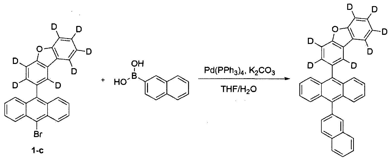
3구 플라스크에 화합물 l-c(12.5 g, 29.0 瞧 ol), 나프탈렌 -2- 일보론산 (5.5 g, 32.0 mmol)을 THF(190 ml)에 녹이고 K2C03(16.1 g, 116.2 麵 ol)을 물 (94 nil)에 녹여 넣었다. 여기에 Pd(PPh3)4(1.3 g, 1.2 隱 ol)를 넣고, 아르곤 분위기 환류 조건 하에서 8사간 동안 교반하였다ᅳ 반응이 종료되면 상온으로 넁각한 후, 반웅액을 분액 깔대기에 옮기고, 물과. 에틸 아세테이트로 추출하였다. 추출액을 MgS04로 건조 후, 여과 및 농축한 후, 시료를 실리카 겔 컬럼 크로마토그래피로 정제한 후, 승화 정제를 통해 화합물 1을 수득하였다 (4..9 g, 수율 35%, MS: [M+H]+= 478). In a three-necked flask, compound lc (12.5 g, 29.0 μl ol), naphthalene-2-ylboronic acid (5.5 g, 32.0 mmol) was dissolved in THF (190 ml), and K 2 CO 3 (16.1 g, 116.2 μl) was dissolved in water. Dissolved in (94 nil). Pd (PPh 3 ) 4 (1.3 g, 1.2 隱 ol) was added thereto, and the mixture was stirred for 8 hours under reflux condition under argon atmosphere. After completion of the reaction, the reaction solution was cooled to room temperature and the reaction solution was transferred to a separatory funnel. . Extracted with ethyl acetate. The extract was dried over MgSO 4 , filtered and concentrated, the sample was purified by silica gel column chromatography, and then sublimed to obtain Compound 1 (4..9 g, yield 35%, MS: [M]. + H] + = 478).


단계 1) 화합물 5— a의 제조 Step 1) Preparation of Compound 5—a

3구 플라스크에 9-브로모안트라센 (14.0 g, 54.4 瞧 ol), 중간체 B(13.1 g, 59.9 睡 ol)을 THF(210 ml)에 녹이고 K2C03(30.1 g, 217.8 隱 ol)을 물 (105 ml)에 녹여 넣었다. 여기에 Pd(PPh3)4(2.5g, 2.2瞧01)를 넣고, 아르곤 분위기 환류 조건 하에서 8시간 동안 교반하였다. 반웅이 종료되면 상온으로 냉각한 후, 반웅액을 분액 깔대기에 옮기고, 물과 에틸 아세테이트로 추출하였다. 추출액을 MgS04로 건조 후, 여과 및 농축한 후, 시료를. 실리카 겔 컬럼 크로마토그래피로 정제하여 화합물 5-a를 수득하였다 (14.4 g. 수율 75%, MS: [M+H]+= 351). In a three-necked flask, 9-bromoanthracene (14.0 g, 54.4 μl ol) and intermediate B (13.1 g, 59.9 μl ol) were dissolved in THF (210 ml) and K 2 CO 3 (30.1 g, 217.8 μl ol) was watered. (105 ml) was dissolved. Pd (PPh 3 ) 4 (2.5 g, 2.2 瞧0 1) was added thereto, and the mixture was stirred for 8 hours under reflux condition of argon atmosphere. After the reaction was completed, the reaction mixture was cooled to room temperature, and the reaction solution was transferred to a separatory funnel, and extracted with water and ethyl acetate. The extract was dried over MgS0 4 , filtered and concentrated, and then sampled. Purification by silica gel column chromatography gave compound 5-a (14.4 g. Yield 75%, MS: [M + H] + = 351).

2구 플라스크에 화합물 5— a(14.0 g, 39.8 隱 ol), NBS(7.4 g, 41.8 麵 ol), DMF(280 ml)를 넣고, 아르곤 분위기 하에서 상온에서 8시간 동안 교반하였다. 반응 종료 후, 반응액을 분액 깔대기에 옮기고. 물과 에틸 아세테이트로 유기충을 추출하였다. 추출액을 MgS04로 건조하고, 여과 및. 농축한 후, 시료를 실리카 겔 컬럼 크로마토그래피로 정제하여 화합물 5- b를 수득하였다 (13.2 g, 수율 77%, MS: [M+H]+= 403). 단계 3) 화합물 5의 제조 Compound 5—a (14.0 g, 39.8 μl ol), NBS (7.4 g, 41.8 μl ol) and DMF (280 ml) were added to a two neck flask and stirred for 8 hours at room temperature under an argon atmosphere. After the reaction was completed, the reaction solution was transferred to a separatory funnel. The organic insects were extracted with water and ethyl acetate. The extract was dried over MgSO 4 , filtered and filtered. After concentration, the sample was purified by silica gel column chromatography to give compound 5-b (13.2 g, yield 77%, MS: [M + H] + = 403). Step 3) Preparation of Compound 5


실시예 1의 단계 4에서, 화합물 1-c 대신 화합ᅵ물 5-b를 사용하고, 나프탈렌 -2-일보론산 대신 나프탈렌— 1-일보론산을 사용한 것을 제외하고는, 화합물 1의 제조 방법과 동일한 방법으로 화합물 6을 제조하였다 (4.4 g, 수율 32%, MS: [M+H]+= 478). 실시예 7: 화합물 7의 제조 In Step 4 of Example 1, the same method as for preparing Compound 1, except that Compound 5-b was used instead of Compound 1-c and naphthalene- 1- ylboronic acid was used instead of naphthalene-2- ylboronic acid Compound 6 was prepared by the method (4.4 g, yield 32%, MS: [M + H] + = 478). Example 7: Preparation of Compound 7

7 7
실시예 1의 단계 4에서, 화합물 1-c 대신 화합물 5— b를 사용하고, 나프탈렌 -2-일보론산 대신 (6-페닐나프탈렌 -2-일)보론산을 사용한 것을 제외하고는, 화합물 1의 제조 방법과 동일한 방법으로 화합물 7을 제조하였다 (5.0 g, 수율 31%, MS: M+H]+- 554). In Step 4 of Example 1, except that Compound 5-b was used instead of Compound 1-c and (6-phenylnaphthalen-2-yl) boronic acid was used instead of naphthalen-2-ylboronic acid, Compound 7 was prepared by the same method as the preparation method (5.0 g, yield 31%, MS: M + H] + -554).

실시예 1의 단계 4에서, 화합물 1-c 대신 화합물 5-b를 사용하고, 나프탈렌 -2-일보론산 대신 트리페닐렌— 2-일보론산을 사용한 것을 제외하고는, 화합물 1의 제조 방법과 동일한 방법으로 화합물 8을 '제조하였다 (6.2 g, 수율 37%, MS: [M+H]+= 578). 실시예 9: 화합물 9의 제조 In step 4 of Example 1, the same method as for preparing compound 1, except that compound 5-b was used instead of compound 1-c and triphenylene- 2-ylboronic acid was used instead of naphthalene-2-ylboronic acid Compound 8 was prepared ' by the method (6.2 g, yield 37%, MS: [M + H] + = 578). Example 9: Preparation of Compound 9
단계 1) 화합물 9— a의 제조

3구 플라스크에 화합물 1— a(15.0 g, 49.3 mmol), 중간체 C(25.5 g. 54.2 隱 ol)을 THFC225 ml)에 녹이고, 2C03(27.3 g, 197.2 mmol)을 물 (113 ml)에 녹여 넣었다. 여기에 Pd(PPh3)4(2.3 g, 2.0 隱 ol)를 넣고, 아르곤 분위기 환류 조건 하에서 8시간 동안 교반하였다. 반응이 종료되면 상온으로 넁각한 후. 반웅액을 분액 깔대기에 옮기고, 물과 에틸 아세테이트로 추출하였다. 추출액을 MgS04로 건조 후, 여과 및 농축한 후, 시료를 실리카 겔 컬럼 크로마토그래피로 정제하여 화합물 9—a를 수득하였다 (11ᅳ 6 g, 수율 68%, MS: [M+H]+= 347). In a three-necked flask, dissolve Compound 1—a (15.0 g, 49.3 mmol), Intermediate C (25.5 g. 54.2 μl) in THFC225 ml, and 2 CO 3 (27.3 g, 197.2 mmol) in water (113 ml). Melted. Pd (PPh 3 ) 4 (2.3 g, 2.0 Pa ol) was added thereto and stirred for 8 hours under argon atmosphere reflux conditions. When the reaction is over, after cooling to room temperature. The reaction solution was transferred to a separatory funnel and extracted with water and ethyl acetate. The extract was dried over MgSO 4 , filtered and concentrated, and the sample was purified by silica gel column chromatography to give compound 9-a (11 ᅳ 6 g, yield 68%, MS: [M + H] + = 347).

실시예 1의 단계 3에서, 화합물 1-b 대신 화합물 9-a를 사용한 것을 제외하고는, 화합물 1-c의 제조 방법과 동일한 방법으로 화합물 9-b를 제조하였다 (11.9 g, 수율 88%, MS: [M+H]+= 426). 단계 3) 화합물' 9의 제조

9 9
실시예 1의 단계 4에서, 화합물 1— c 대신 화합물 9-b를 사용한 것을 제외하고는, 화합물 1의 제조 방법과 동일한 방법으로 화합물 9를 제조하였다 (4.3 g, 수율 34%, MS: [M+H]+= 474). 실시예 10: 화합물 10의 제조 In Step 4 of Example 1, except that Compound 9-b was used instead of Compound 1-c, Compound 9 was prepared by the same method as the preparation of Compound 1 (4.3 g, Yield 34%, MS: [M + H] + = 474). Example 10 Preparation of Compound 10

실시예 1의 단계 4에서, 화합물 1-c 대신 화합물 9-b를 사용하고, 나프탈렌 -2_일보론산 대신 페난쓰렌ᅳ 9-일보론산을 사용한 것을 제외하고는, 화합물 1의 제조 방법과 동일한 방법으로 화합물 10을 제조하였다 (4.4 g. 수율 31%, MS: [M+H]+= 524). 실시예 11: 화합물 11의 제조 In Example 1 step 4, the compound 1-c instead of using the compound 9-b, and naphthalene-2 and _ the same procedures as in the process for producing the compound 1, but instead of daily acid was used to form the 9-phenanthryl sseuren eu Daily acid Compound 10 was prepared (4.4 g. Yield 31%, MS: [M + H] + = 524). Example 11: Preparation of Compound 11

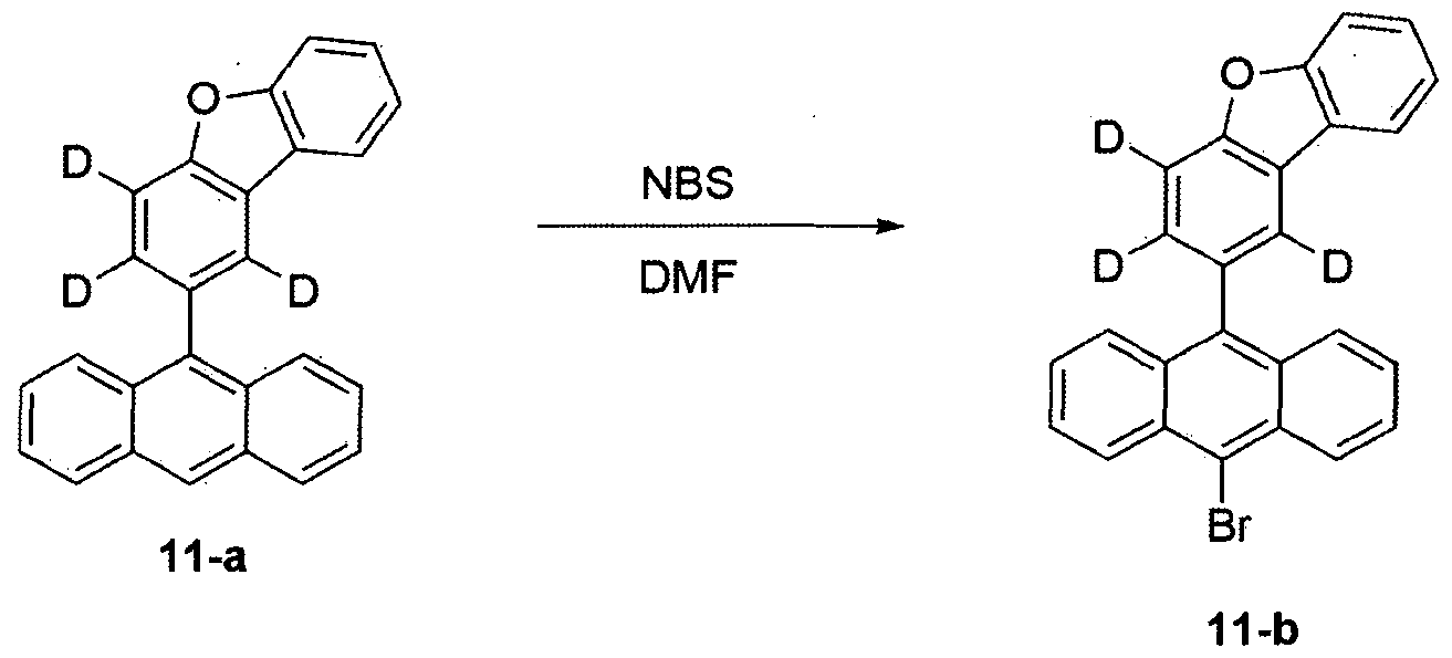
실시예 1의 단계 3에서, 화합물 1-b 대신 화합물 11-a를 사용한 것을 제외하고는, 화합물 1-c의 제조 방법과 동일한 방법으로 화합물 11-b를 제조하였다 (11.5 g, 수율 85%, MS: [M+H]+= 426). In Step 3 of Example 1, except that Compound 11-a was used instead of Compound 1-b, Compound 11-b was prepared by the same method as the method for preparing Compound 1-c (11.5 g, 85% yield, MS: [M + H] + = 426).

실시예 1의 단계 4에서, 화합물 1-c 대신 화합물 11— b를 사용한 것을 제외하고는, 화합물 1의 제조 방법과 동일한 방법으로 화합물 11을 제조하였다 (4.5 g, 수율 35%, MS: [M+H]+= 474). 실시예 12: 화합물 12의 제조 In Step 4 of Example 1, except that Compound 11-b was used instead of Compound 1-c, Compound 11 was prepared by the same method as the preparation of Compound 1 (4.5 g, 35% yield, MS: [M]. + H] + = 474). Example 12: Preparation of Compound 12

^

13 13
실시예 11에서, 중간체 D 대신 중간체 E를 사용하고, 나프탈렌 -2- 일보론산 대신 페난쓰렌 -9-일보론산을 사용한 것을 제외하고는, 화합물 11의 제조 방법과 동일한 방법으로 화합물 13을 제조하였다 (4.3 g, MS: [M+H] = 525). In Example 11, Compound 13 was prepared by the same method as the method for preparing Compound 11, except that Intermediate E was used instead of Intermediate D, and phenanthren-9-ylboronic acid was used instead of naphthalene-2-ylboronic acid. 4.3 g, MS: [M + H] = 525).

실시예 11에서 중간체 D 대신 중간체 E& 사용하고, 나프탈렌—2— 일보론산 대신 나프탈렌— 1-일보론산을 사용한 것을 제외하고는, 화합물 11의 제조 방법과 동일한 방법으로 화합물 14를 제조하였다 (4.5 g, MS: [M+H]+= 475). 실시예 15: 화합물 15의 제조 Compound 14 was prepared in the same manner as in the preparation of Compound 11, except that Intermediate E & was used instead of Intermediate D in Example 11, and naphthalene- 1-ylboronic acid was used instead of naphthalene—2—ilboronic acid (4.5 g, MS: [M + H] + = 475). Example 15: Preparation of Compound 15


15 15
실시예 11에서, 중간체 D 대신 중간체 F를 사용한 것을 제외하고는. 화합물 11의 제조 방법과 동일한 방법으로 화합물 15를 제조하였다 (5.3 g. MS: [M+H]+= 494), In Example 11, except that Intermediate F was used instead of Intermediate D. Compound 15 was prepared by the same method as the compound 11 preparation (5.3 g. MS: [M + H] + = 494),
[실험예] Experimental Example
실험예 1 Experimental Example 1
IT0( Indium Tin Oxide)가 1,400A의 두께로 박막 코팅된 유리기판을 세제에 녹인 증류수에 넣고 초음파로 세척하였다. 이때 세제로는 피셔사 (Fischer Co.)의 Decon™ C0N705 제품을 사용하였으며, 증류수로는 밀러포어사 (Millipore Co.) 제품의 0.22 sterilizing filter로 2차 걸러진 증류수를 사용하였다. IT0를 30분간 세척한 후 증류수로 2회 반복하여 초음파 세척을 10분간 진행하였다. 증류수 세척이 끝난 후, 이소프로필 알코올, 아세톤 및 메탄올의 용제로 각각 10분간 초음파 세착하고, 건조시킨 후 플라즈마 세정기로 수송시켰다. 또한 산소 플라즈마를 이용하여 상기 기판을 5분간 세정한 후, 진공 증착기로 기판을 수송시켰다. 이렇게 준비된 ΠΌ 투명 전극 위에 하기 HI— Α 화합물과 하기 HATᅳ CN 화합물을 각각 650 A의 두께 및 50 A의 두께로 순차적으로 열 진공 증착하여 정공주입층을 형성하였다. 상기 정공주입층 상에 하기 HT-A 화합물을 600A 두께로 진공 증착하여 정공수송층을 형성하였다. 상기 정공수송층 상에 하기 HT— B 화합물을 50A의 두께로 열 진공 증착하여 전자저지층을 형성하였다. 상기 전자저지층 상에 앞서 제조한 화합물 1과 하기 BD 화합물을 96 : 4의 중량비로 200 A의 두께로 진공 증착하여 발광층을 형성하였다. 상기 발광충 상에 하기 ET— A 화합물을 50A의 두께로 진공 증착하여 정공저지층을 형성하였다. 상기 정공저지충 상에 하기 ET-B 화합물과 하기 Liq 화합물을 1 : 1의 중량비로 310A의 두께로 열 진공 증착하여 전자수송층을 형성하였다. 상기 전자수송층 상에 하기 L i q 화합물을 5A의 두께로 진공 증착하여 전자주입층을 형성하였다. 상기 전자주입층 상에 순차적으로 마그네슘과 은을 10 : 1의 중량비로 120A의 두께로, 알루미늄을 1000A 두께로 증착하여 음극올 형성하여, 유기 발광 소자를 제조하였다. IT0 (Indium Tin Oxide) was a thin film coated glass substrate with a thickness of 1,400A was put in distilled water dissolved in detergent and washed with ultrasonic waves. Fischer Co.'s Decon ™ C0N705 product was used as a detergent, and distilled water was filtered secondly with a 0.22 sterilizing filter of Millerpore Co.'s product. After washing IT0 for 30 minutes, the ultrasonic cleaning was performed twice with distilled water for 10 minutes. After washing the distilled water, ultrasonic washing with a solvent of isopropyl alcohol, acetone and methanol for 10 minutes, dried and then transported to a plasma cleaner. In addition, the substrate was cleaned for 5 minutes using an oxygen plasma, and then the substrate was transferred to a vacuum evaporator. The following HI—Α compound and the following HAT ′ CN compound were thermally vacuum deposited to a thickness of 650 A and a thickness of 50 A, respectively, on the πΌ transparent electrode thus prepared to form a hole injection layer. The following HT-A compound was vacuum deposited to a thickness of 600 A on the hole injection layer to form a hole transport layer. The following HT—B compound was thermally vacuum deposited to a thickness of 50 A on the hole transport layer to form an electron blocking layer. The light emitting layer was formed by vacuum depositing Compound 1 and the following BD compound on the electronic blocking layer at a thickness of 200 A at a weight ratio of 96: 4. The following ET-A compound was vacuum-deposited to a thickness of 50 A on the luminescent charge to form a hole blocking layer. The following ET-B compound and the following Liq compound were thermally vacuum-deposited to a thickness of 310 A on a weight ratio of 1: 1 to form an electron transport layer on the hole blocking layer. The following L iq compound was vacuum deposited to a thickness of 5 A on the electron transport layer to form an electron injection layer. Magnesium and silver were sequentially deposited on the electron injection layer at a weight ratio of 10: 1 to 120A, and aluminum was deposited to 1000A to form a cathode, thereby manufacturing an organic light emitting device.


실험예 2내지 15 Experimental Examples 2 to 15
상기 실험예 1에서 화합물 1 대신 하기 표 1에 기재된 화합물을 사용한 것을 제외하고는, 상기 실험예 1과 동일한 방법으로 유기 발광 소자를 제조하였다. 비교실험예 1내지 8 An organic light-emitting device was manufactured in the same manner as in Experimental Example 1, except that the compound shown in Table 1 was used instead of the compound 1 in Experimental Example 1. Comparative Experiments 1 to 8
상기 실험예 1에서 화합물 1 대신 하기 표 1에 기재된 화합물을 사용한 것을 제외하고는, 상기 실험예 1과 동일한 방법으로 유기 발광 소자를 제조하였다. 하기 표 1에서, BH-A, BH-B, BH-C, BH-D, BH-E, BH-F, BH-G 및 BH-H의 화합물은 각각 하기와 같다. An organic light emitting diode was manufactured according to the same method as Experimental Example 1 except for using the compound described in Table 1 below instead of compound 1 in Experimental Example 1. In Table 1 below, the compounds of BH-A, BH-B, BH-C, BH-D, BH-E, BH-F, BH-G and BH-H are as follows.


BH-E BH-F BH-G BH-H 상기 실험예 및 비교실험예에서 제조한 유기 발광 소자에 전류를 인가하여, 전압, 효율, 수명 (T95)을 측정하고 그 결과를 하기 표 1에 나타내었다ᅳ 이때, 전압, 효율은 10 mA/cm2의 전류 밀도를 인가하여 측정되었으며, T95은 전류 밀도 20 mA/cm2에서 초기 휘도가 95%로 저하할 때까지의 시간을 의미한다 . BH-E BH-F BH-G BH-H Applying a current to the organic light emitting device manufactured in the above Experimental Example and Comparative Experimental Example to measure the voltage, efficiency, lifetime (T95) and the results are shown in Table 1 below. In this case, the voltage and efficiency were measured by applying a current density of 10 mA / cm 2 , and T95 means the time until the initial luminance decreased to 95% at a current density of 20 mA / cm 2 .
【표 1] [Table 1]
호스 전압 (V) 효율 ( cd/A) 수명 (T95 , hr ) . 물질 (@10mA/cm2) (@10mA/cm2) (@20mA/cni2) 실험예 1 화합물 1 3.32 6.07 65 실험예 2 화합물 2 3.31 6.03 60 실험예 3 화합물 3 3.33 6.08 66 실험예 4 화합물 4 3.34 6. 11 68 실험예 5 화합물 5 3.44 6.07 67 실험예 6 화합물 6 3.45 6.09 65 실험예 7 화합물 7 3.48 6. 10 63 실험예 8 화합물 8 3.44 6.06 61 실험예 9 화합물 9 3.35 5.71 55 실험예 10 화합물 10 3.34 5.66 53 실험예 11 화합물 11 3.30 5.88 59 실험예 12 화합물 12 3.39 5.80 58 실험예 13 화합물 13 3.38 5.55 51 실험예 14 화합물 14 3.36 5.56 50 실험예 15 화합물 15 3.33 6.02 60 비교실험예 1 BH-A 4.25 5. 13 40 비교실험예 2 BH-B 3.81 5. 10 20 비교실험예 3 BH-C 3.71 5.21 20 비교실험예 4 BH-D 4.81 3. 12 10 비교실험예 5 BH-E 4.80 3.51 13 비교실험예 6 BH-F 5.28 2. 12 5 비교실험예 7 BH-G 3.31 5. 10 40 비교실험예 8 BH-H 3.35 5.06 41 비교실험예 1의 BH-A 구조와 비교해볼 때, 디벤조퓨란이나 디벤조티오펜이 안트라센에 직접 결합한 경우 그렇지 않은 경우보다 HOMO 에너지 레벨이 더 높아지고 hole의 주입이 용이하여 구동 전압이 낮아지는 효과가 있었다. 비교실험예 2 및 비교실험예 3에서 볼 수 있듯이, BH-B나 BH-C와 같이 디벤조퓨란이나 디벤조티오펜이 안트라센에 직접 결합하여 있다고 하더라도 그 맞은편에 페닐기만 있는 경우는 분자량이 너무 작아 열안정성이 떨어지고 이는 효율 및 수명의 저하로 나타났다. 열안정성 확보를 위해 디벤조퓨란에 치환기 ¾ 도입하여 분자량을 키운 BH-D . BH-E , BH-F가 적용된 비교실험예 4. 비교실험예 5 , 비교실험예 6의 경우는. 오히려 전압 상승, 효율 저하, 수명 저하의 결과로 이어졌다. 상기의 결과로 미루어볼 때 화학식 1의 구조와 같이 디벤조퓨란이나 디벤조티오펜이 안트라센에 직접 결합하고, 맞은편에 탄소수 10 내지 탄소수 20의 아릴기가 오는 것이 청색 발광층 호스트로 적절한 구조임을 확인할 수 있다. 또한, 중수소는 수소보다 높은 원자량을 가지고 있어 작은 진동 모드를 갖고 이는 들뜬 상태에서의 비 방사성 감쇠 시간을 늘려, 특히 삼증항 여기자의 안정성을 높인다. 삼중항 여기자의 높아진 안정성은 결국 TTF 현상을 증폭시켜 청색 형광의 효율 및 수명 향상에 기여할 수 있다. 표 1에 기재된 실험예 1 내지 실험예 15의 결과는 중수소가 치환되지 않은 비교실험예 7 및 비교실험예 8과 비교해볼 때 그러한 효과를 잘 나타낸다. 또한, 실험예들의 결과로부터 디벤조퓨란이나 디벤조티오펜에 중수소가 많을수록, 중수소의 위치가 삼중항 여기자가 주로 위치하는 안트라센에 가까울수록 그 효과는 커짐을 알 수 있다. 결과적으로 화학식 1의 구조를 갖는 물질을 유기 전계 발광 소자의 청색 발광층 호스트로 사용하였을 때, 저전압, 고효율, 장수명의 소자를 얻을 수 있다. Hose Voltage (V) Efficiency (cd / A) Life (T95, hr) . Substance (@ 10 mA / cm 2 ) (@ 10 mA / cm 2 ) (@ 20 mA / cni 2 ) Experimental Example 1 Compound 1 3.32 6.07 65 Experimental Example 2 Compound 2 3.31 6.03 60 Experimental Example 3 Compound 3 3.33 6.08 66 Experimental Example 4 Compound 4 3.34 6. 11 68 Experiment 5 Compound 5 3.44 6.07 67 Experiment 6 Compound 6 3.45 6.09 65 Experiment 7 Compound 7 3.48 6. 10 63 Experiment 8 Compound 8 3.44 6.06 61 Experiment 9 Compound 9 3.35 5.71 55 Experiment 10 Compound 10 3.34 5.66 53 Experiment 11 Compound 11 3.30 5.88 59 Experiment 12 Compound 12 3.39 5.80 58 Experimental Example 13 Compound 13 3.38 5.55 51 Experimental Example 14 Compound 14 3.36 5.56 50 Experimental Example 15 Compound 15 3.33 6.02 60 Comparative Experiment 1 BH-A 4.25 5. 13 40 Comparative Experiment 2 BH-B 3.81 5. 10 20 Comparative Experiment Example 3 BH-C 3.71 5.21 20 Comparative Experiment 4 BH-D 4.81 3. 12 10 Comparative Experiment 5 BH-E 4.80 3.51 13 Comparative Experiment 6 BH-F 5.28 2. 12 5 Comparative Experiment 7 BH-G 3.31 5. 10 40 Comparative Example 8 BH-H 3.35 5.06 41 Compared with the BH-A structure of Comparative Example 1, the HOMO energy level was higher than when the dibenzofuran or dibenzothiophene was directly bonded to the anthracene. Higher and easier injection of holes, the driving voltage was lowered. As seen in Comparative Experiment 2 and Comparative Example 3, even if dibenzofuran or dibenzothiophene is directly bonded to anthracene, such as BH-B or BH-C, when there is only a phenyl group on the opposite side, the molecular weight is Too small to reduce thermal stability, which resulted in reduced efficiency and lifetime. BH-D increased molecular weight by introducing substituent ¾ to dibenzofuran to ensure thermal stability. Comparative Experimental Example with BH-E and BH-F applied 4. Comparative Experimental Example 5 and Comparative Experimental Example 6 are . Rather, it resulted in higher voltage, lower efficiency, and lower lifetime. As a result of the above results, it is confirmed that a dibenzofuran or a dibenzothiophene is directly bonded to anthracene, and an aryl group having 10 to 20 carbon atoms is opposite to the blue light emitting layer host. have. In addition, deuterium has a higher atomic weight than hydrogen and thus has a small oscillation mode, which increases the non-radioactive decay time in the excited state, and in particular, increases the stability of the triplet excitons. The increased stability of triplet excitons can eventually amplify the TTF phenomenon and contribute to the efficiency and lifetime improvement of blue fluorescence. The results of Experimental Examples 1 to 15 described in Table 1 show such effects well when compared with Comparative Experimental Example 7 and Comparative Experimental Example 8 in which deuterium is not substituted. From the results of the experimental examples, the more deuterium is contained in dibenzofuran or dibenzothiophene, the more the deuterium is located in the anthracene where the triplet excitons are mainly located. The closer it is, the greater the effect. As a result, when the material having the structure of Formula 1 is used as the blue light emitting layer host of the organic electroluminescent device, a low voltage, high efficiency, long life device can be obtained.
【부호의 설명】 [Explanation of code]
1: 기판 2: 양극 1: substrate 2: anode
3: 발광층 4: 음극 3: light emitting layer 4: cathode
5: 정공 주입층 6: 정공 수송층 5: hole injection layer 6: hole transport layer
7: 발광층 8: 전자 수송층 7: light emitting layer 8: electron transport layer
Claims
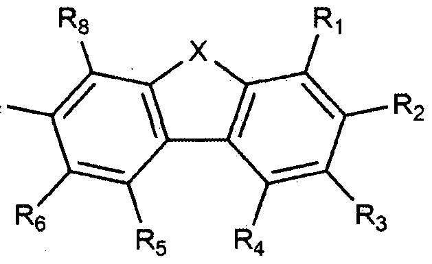


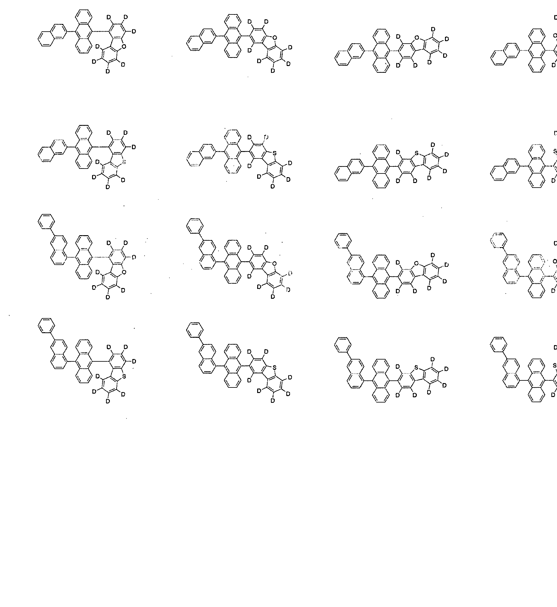


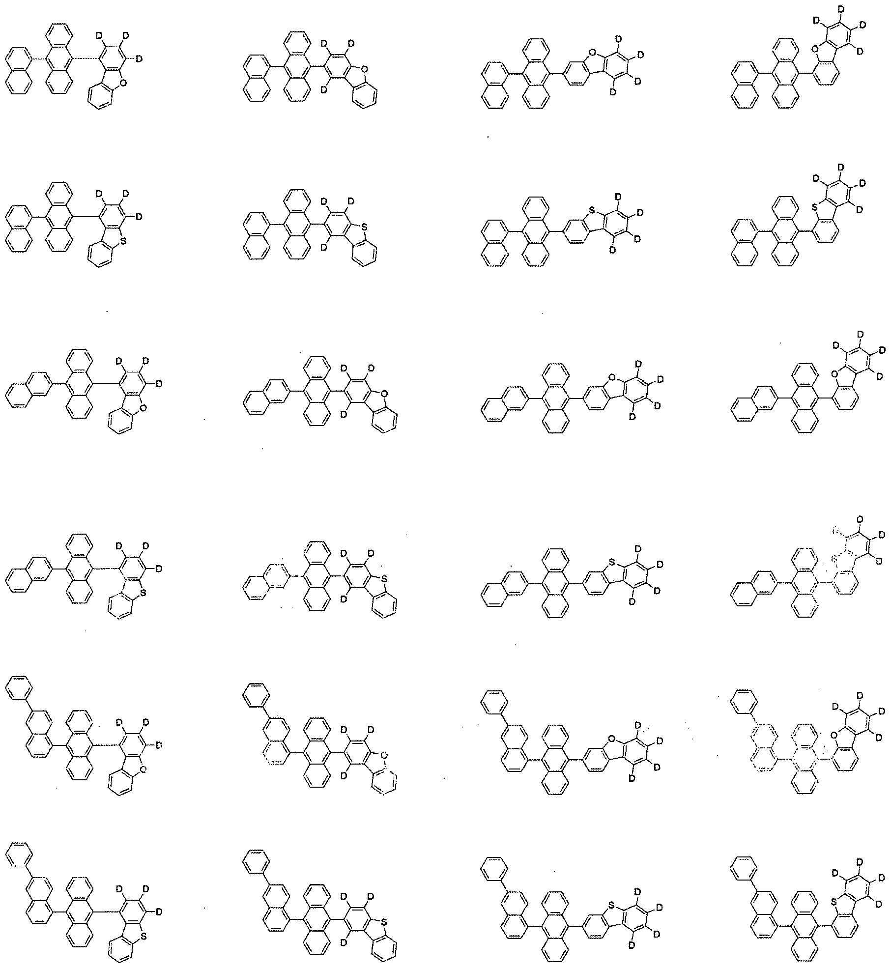

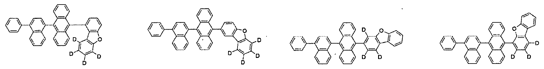


Priority Applications (1)
| Application Number | Priority Date | Filing Date | Title |
|---|---|---|---|
| CN201780038040.7A CN109415333B (en) | 2016-12-14 | 2017-12-06 | Heterocyclic compound and organic light-emitting element comprising same |
Applications Claiming Priority (2)
| Application Number | Priority Date | Filing Date | Title |
|---|---|---|---|
| KR10-2016-0170676 | 2016-12-14 | ||
| KR20160170676 | 2016-12-14 |
Publications (1)
| Publication Number | Publication Date |
|---|---|
| WO2018110887A1 true WO2018110887A1 (en) | 2018-06-21 |
Family
ID=62559127
Family Applications (1)
| Application Number | Title | Priority Date | Filing Date |
|---|---|---|---|
| PCT/KR2017/014194 Ceased WO2018110887A1 (en) | 2016-12-14 | 2017-12-06 | Heterocyclic compound, and organic light-emitting element comprising same |
Country Status (3)
| Country | Link |
|---|---|
| KR (1) | KR101964435B1 (en) |
| CN (1) | CN109415333B (en) |
| WO (1) | WO2018110887A1 (en) |
Cited By (43)
| Publication number | Priority date | Publication date | Assignee | Title |
|---|---|---|---|---|
| WO2020080714A1 (en) * | 2018-10-16 | 2020-04-23 | 주식회사 엘지화학 | Organic compound and organic light-emitting device comprising same |
| WO2020085845A1 (en) * | 2018-10-26 | 2020-04-30 | Rohm And Haas Electronic Materials Korea Ltd. | Organic electroluminescent compound and organic electroluminescent device comprising the same |
| CN111564558A (en) * | 2020-05-14 | 2020-08-21 | 苏州大学 | Preparation method of organic crystalline film and organic field effect transistor |
| JP2023505832A (en) * | 2020-08-27 | 2023-02-13 | エルジー・ケム・リミテッド | Method for producing deuterated aromatic compounds and deuterated reaction composition |
| WO2023061998A1 (en) | 2021-10-14 | 2023-04-20 | Merck Patent Gmbh | Materials for organic electroluminescent devices |
| WO2023078812A1 (en) | 2021-11-02 | 2023-05-11 | Merck Patent Gmbh | Benzofuro[3,2-d]pyrimidino-2,4-dicarbonitril derivatives and similar compounds for organic electroluminescence devices |
| WO2023099430A1 (en) | 2021-12-02 | 2023-06-08 | Merck Patent Gmbh | Triphenylene-triazine-dibenzofuran/dibenzothiophene derivatives for organic electroluminescent devices |
| WO2023125667A1 (en) * | 2021-12-30 | 2023-07-06 | Arthrosi Therapeutics, Inc. | Preparation of a compound for the treatment of gout or hyperuricemia |
| WO2024038068A1 (en) | 2022-08-19 | 2024-02-22 | Merck Patent Gmbh | Materials for organic electroluminescent devices |
| WO2024038029A1 (en) | 2022-08-17 | 2024-02-22 | Merck Patent Gmbh | Materials for organic electroluminescent devices |
| WO2024104934A1 (en) | 2022-11-16 | 2024-05-23 | Merck Patent Gmbh | Materials for organic electroluminescent devices |
| WO2024121133A1 (en) | 2022-12-08 | 2024-06-13 | Merck Patent Gmbh | Organic electronic device and special materials for organic electronic devices |
| WO2024133211A1 (en) | 2022-12-21 | 2024-06-27 | Merck Patent Gmbh | Novel materials for organic electroluminescent devices |
| WO2024132993A1 (en) | 2022-12-19 | 2024-06-27 | Merck Patent Gmbh | Materials for electronic devices |
| WO2024194264A1 (en) | 2023-03-20 | 2024-09-26 | Merck Patent Gmbh | Materials for organic electroluminescent devices |
| WO2024218109A1 (en) | 2023-04-20 | 2024-10-24 | Merck Patent Gmbh | Materials for electronic devices |
| US12145917B2 (en) | 2018-12-06 | 2024-11-19 | Arthrosi Therapeutics, Inc. | Crystalline forms of a compound for treating or preventing gout or hyperuricemia |
| WO2024251699A1 (en) | 2023-06-07 | 2024-12-12 | Merck Patent Gmbh | Materials for organic electroluminescent devices |
| WO2025021855A1 (en) | 2023-07-27 | 2025-01-30 | Merck Patent Gmbh | Materials for organic light-emitting devices and organic sensors |
| WO2025021785A1 (en) | 2023-07-25 | 2025-01-30 | Merck Patent Gmbh | Organic electronic device |
| WO2025021841A1 (en) | 2023-07-27 | 2025-01-30 | Merck Patent Gmbh | Organic electronic device |
| WO2025045843A1 (en) | 2023-08-30 | 2025-03-06 | Merck Patent Gmbh | Materials for organic light-emitting devices |
| WO2025045816A1 (en) | 2023-08-29 | 2025-03-06 | Merck Patent Gmbh | Materials for organic electroluminescent devices |
| WO2025051664A1 (en) | 2023-09-04 | 2025-03-13 | Merck Patent Gmbh | Materials for organic light-emitting devices |
| WO2025051734A1 (en) | 2023-09-06 | 2025-03-13 | Merck Patent Gmbh | Materials for organic electroluminescent devices |
| WO2025073675A1 (en) | 2023-10-04 | 2025-04-10 | Merck Patent Gmbh | Materials for organic electroluminescent devices |
| WO2025087892A1 (en) | 2023-10-25 | 2025-05-01 | Merck Patent Gmbh | Novel materials for organic electroluminescent devices |
| WO2025104058A1 (en) | 2023-11-16 | 2025-05-22 | Merck Patent Gmbh | Materials for organic electronic devices |
| WO2025125168A1 (en) | 2023-12-12 | 2025-06-19 | Merck Patent Gmbh | Materials for organic electroluminescent devices |
| WO2025125125A1 (en) | 2023-12-12 | 2025-06-19 | Merck Patent Gmbh | Organic electronic device |
| WO2025125167A1 (en) | 2023-12-11 | 2025-06-19 | Merck Patent Gmbh | Materials for organic electroluminescent devices |
| WO2025132524A1 (en) | 2023-12-22 | 2025-06-26 | Merck Patent Gmbh | Novel materials for organic electroluminescent devices |
| WO2025132194A1 (en) | 2023-12-20 | 2025-06-26 | Merck Patent Gmbh | Novel materials for organic electroluminescent devices |
| WO2025140947A1 (en) | 2023-12-28 | 2025-07-03 | Merck Patent Gmbh | New materials for organic electroluminescent devices |
| WO2025168515A1 (en) | 2024-02-06 | 2025-08-14 | Merck Patent Gmbh | Materials for organic electronic devices |
| US12419854B2 (en) | 2018-12-06 | 2025-09-23 | Arthrosi Therapeutics, Inc. | Methods for treating or preventing gout or hyperuricemia |
| WO2025219233A1 (en) | 2024-04-15 | 2025-10-23 | Merck Patent Gmbh | Materials for organic light-emitting devices |
| WO2025219241A1 (en) | 2024-04-15 | 2025-10-23 | Merck Patent Gmbh | Materials for organic light-emitting devices |
| WO2025228800A1 (en) | 2024-04-30 | 2025-11-06 | Merck Patent Gmbh | Materials for organic electronic devices |
| WO2026017610A1 (en) | 2024-07-15 | 2026-01-22 | Merck Patent Gmbh | Organic light-emitting device |
| WO2026017612A1 (en) | 2024-07-15 | 2026-01-22 | Merck Patent Gmbh | Organic light-emitting device |
| WO2026017607A1 (en) | 2024-07-15 | 2026-01-22 | Merck Patent Gmbh | Organic light-emitting device |
| WO2026017608A1 (en) | 2024-07-15 | 2026-01-22 | Merck Patent Gmbh | Materials for organic light-emitting devices |
Families Citing this family (8)
| Publication number | Priority date | Publication date | Assignee | Title |
|---|---|---|---|---|
| CN111556866B (en) * | 2018-06-08 | 2023-11-14 | 株式会社Lg化学 | Polycyclic compound and organic electronic element including the same |
| US12453284B2 (en) | 2019-10-30 | 2025-10-21 | Lg Chem, Ltd. | Anthracene compound and organic light-emitting device comprising same |
| KR102530091B1 (en) * | 2020-12-11 | 2023-05-09 | 솔루스첨단소재 주식회사 | Organic light-emitting compound and organic electroluminescent device comprising the same |
| KR102767268B1 (en) * | 2021-09-03 | 2025-02-13 | 삼성에스디아이 주식회사 | Compound for organic optoelectronic device, organic optoelectronic device and display device |
| CN115260137B (en) * | 2022-08-02 | 2024-04-09 | Tcl华星光电技术有限公司 | Organic compounds, compositions, and organic electronic devices |
| CN116143740B (en) * | 2023-02-27 | 2025-01-28 | 阜阳欣奕华新材料科技股份有限公司 | Deuterated benzofuran compounds, organic electroluminescent devices and display devices |
| CN117263894A (en) * | 2023-09-22 | 2023-12-22 | 冠能光电材料(深圳)有限责任公司 | An organic compound and an organic light-emitting device containing the same |
| CN118406486B (en) * | 2024-04-28 | 2025-03-21 | 石家庄诚志永华显示材料有限公司 | A blue light-emitting composition and an organic electroluminescent device containing the same |
Citations (7)
| Publication number | Priority date | Publication date | Assignee | Title |
|---|---|---|---|---|
| KR20100109050A (en) * | 2009-03-31 | 2010-10-08 | 다우어드밴스드디스플레이머티리얼 유한회사 | Novel organic electroluminescent compounds and organic electroluminescent device using the same |
| KR20110094271A (en) * | 2009-12-16 | 2011-08-23 | 이데미쓰 고산 가부시키가이샤 | Organic light emitting medium |
| KR20130134205A (en) * | 2012-05-30 | 2013-12-10 | 롬엔드하스전자재료코리아유한회사 | Novel organic light emitting compound and organic electroluminescent device employing the same |
| KR20150007476A (en) * | 2013-07-11 | 2015-01-21 | 덕산하이메탈(주) | Organic electronic element using a compound for organic electronic element, and an electronic device thereof |
| KR20160088229A (en) * | 2015-01-13 | 2016-07-25 | 에스에프씨 주식회사 | organic light-emitting diode with High efficiency and long lifetime |
| KR20160126873A (en) * | 2015-04-23 | 2016-11-02 | 에스에프씨 주식회사 | Organic Compound for organic light emitting diode and an organic light emitting diode including the same |
| KR20160141359A (en) * | 2015-05-27 | 2016-12-08 | 삼성디스플레이 주식회사 | Organic light-emitting device |
Family Cites Families (2)
| Publication number | Priority date | Publication date | Assignee | Title |
|---|---|---|---|---|
| KR100430549B1 (en) | 1999-01-27 | 2004-05-10 | 주식회사 엘지화학 | New organomattalic complex molecule for the fabrication of organic light emitting diodes |
| KR102201097B1 (en) * | 2015-01-20 | 2021-01-11 | 에스에프씨주식회사 | Novel organic compounds for organic light-emitting diode and organic light-emitting diode including the same |
-
2017
- 2017-12-06 CN CN201780038040.7A patent/CN109415333B/en active Active
- 2017-12-06 KR KR1020170166757A patent/KR101964435B1/en active Active
- 2017-12-06 WO PCT/KR2017/014194 patent/WO2018110887A1/en not_active Ceased
Patent Citations (7)
| Publication number | Priority date | Publication date | Assignee | Title |
|---|---|---|---|---|
| KR20100109050A (en) * | 2009-03-31 | 2010-10-08 | 다우어드밴스드디스플레이머티리얼 유한회사 | Novel organic electroluminescent compounds and organic electroluminescent device using the same |
| KR20110094271A (en) * | 2009-12-16 | 2011-08-23 | 이데미쓰 고산 가부시키가이샤 | Organic light emitting medium |
| KR20130134205A (en) * | 2012-05-30 | 2013-12-10 | 롬엔드하스전자재료코리아유한회사 | Novel organic light emitting compound and organic electroluminescent device employing the same |
| KR20150007476A (en) * | 2013-07-11 | 2015-01-21 | 덕산하이메탈(주) | Organic electronic element using a compound for organic electronic element, and an electronic device thereof |
| KR20160088229A (en) * | 2015-01-13 | 2016-07-25 | 에스에프씨 주식회사 | organic light-emitting diode with High efficiency and long lifetime |
| KR20160126873A (en) * | 2015-04-23 | 2016-11-02 | 에스에프씨 주식회사 | Organic Compound for organic light emitting diode and an organic light emitting diode including the same |
| KR20160141359A (en) * | 2015-05-27 | 2016-12-08 | 삼성디스플레이 주식회사 | Organic light-emitting device |
Cited By (47)
| Publication number | Priority date | Publication date | Assignee | Title |
|---|---|---|---|---|
| CN111954666A (en) * | 2018-10-16 | 2020-11-17 | 株式会社Lg化学 | Organic compound and organic light-emitting device comprising the same |
| WO2020080714A1 (en) * | 2018-10-16 | 2020-04-23 | 주식회사 엘지화학 | Organic compound and organic light-emitting device comprising same |
| CN111954666B (en) * | 2018-10-16 | 2023-09-29 | 株式会社Lg化学 | Organic compound and organic light emitting device comprising the same |
| US11864461B2 (en) | 2018-10-16 | 2024-01-02 | Lg Chem, Ltd. | Organic compound and organic light-emitting device comprising same |
| WO2020085845A1 (en) * | 2018-10-26 | 2020-04-30 | Rohm And Haas Electronic Materials Korea Ltd. | Organic electroluminescent compound and organic electroluminescent device comprising the same |
| US12419854B2 (en) | 2018-12-06 | 2025-09-23 | Arthrosi Therapeutics, Inc. | Methods for treating or preventing gout or hyperuricemia |
| US12145917B2 (en) | 2018-12-06 | 2024-11-19 | Arthrosi Therapeutics, Inc. | Crystalline forms of a compound for treating or preventing gout or hyperuricemia |
| CN111564558A (en) * | 2020-05-14 | 2020-08-21 | 苏州大学 | Preparation method of organic crystalline film and organic field effect transistor |
| JP7566023B2 (en) | 2020-08-27 | 2024-10-11 | エルジー・ケム・リミテッド | Method for producing deuterated aromatic compounds and deuterated reaction composition |
| JP2023505832A (en) * | 2020-08-27 | 2023-02-13 | エルジー・ケム・リミテッド | Method for producing deuterated aromatic compounds and deuterated reaction composition |
| WO2023061998A1 (en) | 2021-10-14 | 2023-04-20 | Merck Patent Gmbh | Materials for organic electroluminescent devices |
| WO2023078812A1 (en) | 2021-11-02 | 2023-05-11 | Merck Patent Gmbh | Benzofuro[3,2-d]pyrimidino-2,4-dicarbonitril derivatives and similar compounds for organic electroluminescence devices |
| WO2023099430A1 (en) | 2021-12-02 | 2023-06-08 | Merck Patent Gmbh | Triphenylene-triazine-dibenzofuran/dibenzothiophene derivatives for organic electroluminescent devices |
| WO2023125667A1 (en) * | 2021-12-30 | 2023-07-06 | Arthrosi Therapeutics, Inc. | Preparation of a compound for the treatment of gout or hyperuricemia |
| WO2024038029A1 (en) | 2022-08-17 | 2024-02-22 | Merck Patent Gmbh | Materials for organic electroluminescent devices |
| WO2024038068A1 (en) | 2022-08-19 | 2024-02-22 | Merck Patent Gmbh | Materials for organic electroluminescent devices |
| WO2024104934A1 (en) | 2022-11-16 | 2024-05-23 | Merck Patent Gmbh | Materials for organic electroluminescent devices |
| WO2024121133A1 (en) | 2022-12-08 | 2024-06-13 | Merck Patent Gmbh | Organic electronic device and special materials for organic electronic devices |
| WO2024132993A1 (en) | 2022-12-19 | 2024-06-27 | Merck Patent Gmbh | Materials for electronic devices |
| WO2024133211A1 (en) | 2022-12-21 | 2024-06-27 | Merck Patent Gmbh | Novel materials for organic electroluminescent devices |
| WO2024194264A1 (en) | 2023-03-20 | 2024-09-26 | Merck Patent Gmbh | Materials for organic electroluminescent devices |
| WO2024218109A1 (en) | 2023-04-20 | 2024-10-24 | Merck Patent Gmbh | Materials for electronic devices |
| WO2024251699A1 (en) | 2023-06-07 | 2024-12-12 | Merck Patent Gmbh | Materials for organic electroluminescent devices |
| WO2025021785A1 (en) | 2023-07-25 | 2025-01-30 | Merck Patent Gmbh | Organic electronic device |
| WO2025021855A1 (en) | 2023-07-27 | 2025-01-30 | Merck Patent Gmbh | Materials for organic light-emitting devices and organic sensors |
| WO2025021841A1 (en) | 2023-07-27 | 2025-01-30 | Merck Patent Gmbh | Organic electronic device |
| WO2025045816A1 (en) | 2023-08-29 | 2025-03-06 | Merck Patent Gmbh | Materials for organic electroluminescent devices |
| WO2025045843A1 (en) | 2023-08-30 | 2025-03-06 | Merck Patent Gmbh | Materials for organic light-emitting devices |
| WO2025051664A1 (en) | 2023-09-04 | 2025-03-13 | Merck Patent Gmbh | Materials for organic light-emitting devices |
| WO2025051734A1 (en) | 2023-09-06 | 2025-03-13 | Merck Patent Gmbh | Materials for organic electroluminescent devices |
| WO2025073675A1 (en) | 2023-10-04 | 2025-04-10 | Merck Patent Gmbh | Materials for organic electroluminescent devices |
| WO2025087892A1 (en) | 2023-10-25 | 2025-05-01 | Merck Patent Gmbh | Novel materials for organic electroluminescent devices |
| WO2025104058A1 (en) | 2023-11-16 | 2025-05-22 | Merck Patent Gmbh | Materials for organic electronic devices |
| WO2025125167A1 (en) | 2023-12-11 | 2025-06-19 | Merck Patent Gmbh | Materials for organic electroluminescent devices |
| WO2025125168A1 (en) | 2023-12-12 | 2025-06-19 | Merck Patent Gmbh | Materials for organic electroluminescent devices |
| WO2025125125A1 (en) | 2023-12-12 | 2025-06-19 | Merck Patent Gmbh | Organic electronic device |
| WO2025132194A1 (en) | 2023-12-20 | 2025-06-26 | Merck Patent Gmbh | Novel materials for organic electroluminescent devices |
| WO2025132524A1 (en) | 2023-12-22 | 2025-06-26 | Merck Patent Gmbh | Novel materials for organic electroluminescent devices |
| WO2025140947A1 (en) | 2023-12-28 | 2025-07-03 | Merck Patent Gmbh | New materials for organic electroluminescent devices |
| WO2025168515A1 (en) | 2024-02-06 | 2025-08-14 | Merck Patent Gmbh | Materials for organic electronic devices |
| WO2025219233A1 (en) | 2024-04-15 | 2025-10-23 | Merck Patent Gmbh | Materials for organic light-emitting devices |
| WO2025219241A1 (en) | 2024-04-15 | 2025-10-23 | Merck Patent Gmbh | Materials for organic light-emitting devices |
| WO2025228800A1 (en) | 2024-04-30 | 2025-11-06 | Merck Patent Gmbh | Materials for organic electronic devices |
| WO2026017610A1 (en) | 2024-07-15 | 2026-01-22 | Merck Patent Gmbh | Organic light-emitting device |
| WO2026017612A1 (en) | 2024-07-15 | 2026-01-22 | Merck Patent Gmbh | Organic light-emitting device |
| WO2026017607A1 (en) | 2024-07-15 | 2026-01-22 | Merck Patent Gmbh | Organic light-emitting device |
| WO2026017608A1 (en) | 2024-07-15 | 2026-01-22 | Merck Patent Gmbh | Materials for organic light-emitting devices |
Also Published As
| Publication number | Publication date |
|---|---|
| KR20180068861A (en) | 2018-06-22 |
| CN109415333B (en) | 2022-07-12 |
| CN109415333A (en) | 2019-03-01 |
| KR101964435B1 (en) | 2019-04-01 |
Similar Documents
| Publication | Publication Date | Title |
|---|---|---|
| KR101964435B1 (en) | Hetero-cyclic compound and organic light emitting device comprising the same | |
| KR100867526B1 (en) | New diamine derivatives, preparation method thereof and organic electronic device using the same | |
| KR102040226B1 (en) | Organic light emitting device | |
| JP6066132B2 (en) | Heterocyclic compounds and organic electronic devices containing the same | |
| JP7251711B2 (en) | organic light emitting device | |
| JP6307687B2 (en) | AMINE DERIVATIVE, ORGANIC LIGHT EMITTING MATERIAL AND ORGANIC ELECTROLUMINESCENT DEVICE USING THE SAME | |
| CN103988329B (en) | Material for organic electroluminescent element and organic electroluminescent element using same | |
| KR102044425B1 (en) | Hetero-cyclic compound and organic light emitting device comprising the same | |
| KR101888252B1 (en) | Compound having spiro structure and organic light emitting device comprising the same | |
| WO2018016898A1 (en) | Novel heterocyclic compound and organic light-emitting device using same | |
| KR20210042873A (en) | Organic light emitting device | |
| CN107108545A (en) | Compound for organic light emitting device and organic light emitting device including same | |
| CN112912370B (en) | Polycyclic compound and organic light-emitting element containing the same | |
| KR20150124637A (en) | An electroluminescent compound and an electroluminescent device comprising the same | |
| KR101896151B1 (en) | Compound and organic electronic device using the same | |
| CN113166176A (en) | Compound and organic light-emitting element comprising same | |
| KR100864154B1 (en) | Novel anthracene derivatives, preparation method thereof and organic electronic device using same | |
| KR102088506B1 (en) | Organic light emitting device | |
| KR102054397B1 (en) | Hetero-cyclic compound and organic light emitting device comprising the same | |
| CN111683935B (en) | Heterocyclic compound and organic light-emitting device comprising same | |
| WO2018212435A1 (en) | Organic light emitting device | |
| KR102174388B1 (en) | Cyclic compound and organic light emitting device comprising the same | |
| KR102069311B1 (en) | Hetero-cyclic compound and organic light emitting device comprising the same | |
| KR20210126943A (en) | Anthracene compound and organic light emitting device comprising same | |
| WO2018186662A2 (en) | Organic light-emitting device |
Legal Events
| Date | Code | Title | Description |
|---|---|---|---|
| 121 | Ep: the epo has been informed by wipo that ep was designated in this application |
Ref document number: 17881732 Country of ref document: EP Kind code of ref document: A1 |
|
| NENP | Non-entry into the national phase |
Ref country code: DE |
|
| 122 | Ep: pct application non-entry in european phase |
Ref document number: 17881732 Country of ref document: EP Kind code of ref document: A1 |