WO2005053051A1 - Organic electroluminescent element - Google Patents
Organic electroluminescent element Download PDFInfo
- Publication number
- WO2005053051A1 WO2005053051A1 PCT/EP2004/013315 EP2004013315W WO2005053051A1 WO 2005053051 A1 WO2005053051 A1 WO 2005053051A1 EP 2004013315 W EP2004013315 W EP 2004013315W WO 2005053051 A1 WO2005053051 A1 WO 2005053051A1
- Authority
- WO
- WIPO (PCT)
- Prior art keywords
- organic electroluminescent
- electroluminescent device
- layer
- matrix material
- layers
- Prior art date
- Legal status (The legal status is an assumption and is not a legal conclusion. Google has not performed a legal analysis and makes no representation as to the accuracy of the status listed.)
- Ceased
Links
Classifications
-
- H—ELECTRICITY
- H05—ELECTRIC TECHNIQUES NOT OTHERWISE PROVIDED FOR
- H05B—ELECTRIC HEATING; ELECTRIC LIGHT SOURCES NOT OTHERWISE PROVIDED FOR; CIRCUIT ARRANGEMENTS FOR ELECTRIC LIGHT SOURCES, IN GENERAL
- H05B33/00—Electroluminescent light sources
- H05B33/12—Light sources with substantially two-dimensional radiating surfaces
- H05B33/14—Light sources with substantially two-dimensional radiating surfaces characterised by the chemical or physical composition or the arrangement of the electroluminescent material, or by the simultaneous addition of the electroluminescent material in or onto the light source
-
- C—CHEMISTRY; METALLURGY
- C09—DYES; PAINTS; POLISHES; NATURAL RESINS; ADHESIVES; COMPOSITIONS NOT OTHERWISE PROVIDED FOR; APPLICATIONS OF MATERIALS NOT OTHERWISE PROVIDED FOR
- C09B—ORGANIC DYES OR CLOSELY-RELATED COMPOUNDS FOR PRODUCING DYES, e.g. PIGMENTS; MORDANTS; LAKES
- C09B57/00—Other synthetic dyes of known constitution
- C09B57/10—Metal complexes of organic compounds not being dyes in uncomplexed form
-
- H—ELECTRICITY
- H10—SEMICONDUCTOR DEVICES; ELECTRIC SOLID-STATE DEVICES NOT OTHERWISE PROVIDED FOR
- H10K—ORGANIC ELECTRIC SOLID-STATE DEVICES
- H10K50/00—Organic light-emitting devices
- H10K50/10—OLEDs or polymer light-emitting diodes [PLED]
- H10K50/11—OLEDs or polymer light-emitting diodes [PLED] characterised by the electroluminescent [EL] layers
-
- H—ELECTRICITY
- H10—SEMICONDUCTOR DEVICES; ELECTRIC SOLID-STATE DEVICES NOT OTHERWISE PROVIDED FOR
- H10K—ORGANIC ELECTRIC SOLID-STATE DEVICES
- H10K50/00—Organic light-emitting devices
- H10K50/10—OLEDs or polymer light-emitting diodes [PLED]
- H10K50/17—Carrier injection layers
-
- H—ELECTRICITY
- H10—SEMICONDUCTOR DEVICES; ELECTRIC SOLID-STATE DEVICES NOT OTHERWISE PROVIDED FOR
- H10K—ORGANIC ELECTRIC SOLID-STATE DEVICES
- H10K71/00—Manufacture or treatment specially adapted for the organic devices covered by this subclass
- H10K71/30—Doping active layers, e.g. electron transporting layers
-
- H—ELECTRICITY
- H10—SEMICONDUCTOR DEVICES; ELECTRIC SOLID-STATE DEVICES NOT OTHERWISE PROVIDED FOR
- H10K—ORGANIC ELECTRIC SOLID-STATE DEVICES
- H10K85/00—Organic materials used in the body or electrodes of devices covered by this subclass
- H10K85/60—Organic compounds having low molecular weight
- H10K85/615—Polycyclic condensed aromatic hydrocarbons, e.g. anthracene
- H10K85/626—Polycyclic condensed aromatic hydrocarbons, e.g. anthracene containing more than one polycyclic condensed aromatic rings, e.g. bis-anthracene
-
- H—ELECTRICITY
- H10—SEMICONDUCTOR DEVICES; ELECTRIC SOLID-STATE DEVICES NOT OTHERWISE PROVIDED FOR
- H10K—ORGANIC ELECTRIC SOLID-STATE DEVICES
- H10K2101/00—Properties of the organic materials covered by group H10K85/00
- H10K2101/10—Triplet emission
-
- H—ELECTRICITY
- H10—SEMICONDUCTOR DEVICES; ELECTRIC SOLID-STATE DEVICES NOT OTHERWISE PROVIDED FOR
- H10K—ORGANIC ELECTRIC SOLID-STATE DEVICES
- H10K85/00—Organic materials used in the body or electrodes of devices covered by this subclass
- H10K85/30—Coordination compounds
- H10K85/341—Transition metal complexes, e.g. Ru(II)polypyridine complexes
- H10K85/342—Transition metal complexes, e.g. Ru(II)polypyridine complexes comprising iridium
-
- H—ELECTRICITY
- H10—SEMICONDUCTOR DEVICES; ELECTRIC SOLID-STATE DEVICES NOT OTHERWISE PROVIDED FOR
- H10K—ORGANIC ELECTRIC SOLID-STATE DEVICES
- H10K85/00—Organic materials used in the body or electrodes of devices covered by this subclass
- H10K85/60—Organic compounds having low molecular weight
- H10K85/649—Aromatic compounds comprising a hetero atom
- H10K85/657—Polycyclic condensed heteroaromatic hydrocarbons
- H10K85/6572—Polycyclic condensed heteroaromatic hydrocarbons comprising only nitrogen in the heteroaromatic polycondensed ring system, e.g. phenanthroline or carbazole
-
- Y—GENERAL TAGGING OF NEW TECHNOLOGICAL DEVELOPMENTS; GENERAL TAGGING OF CROSS-SECTIONAL TECHNOLOGIES SPANNING OVER SEVERAL SECTIONS OF THE IPC; TECHNICAL SUBJECTS COVERED BY FORMER USPC CROSS-REFERENCE ART COLLECTIONS [XRACs] AND DIGESTS
- Y02—TECHNOLOGIES OR APPLICATIONS FOR MITIGATION OR ADAPTATION AGAINST CLIMATE CHANGE
- Y02E—REDUCTION OF GREENHOUSE GAS [GHG] EMISSIONS, RELATED TO ENERGY GENERATION, TRANSMISSION OR DISTRIBUTION
- Y02E10/00—Energy generation through renewable energy sources
- Y02E10/50—Photovoltaic [PV] energy
- Y02E10/549—Organic PV cells
Definitions
- the present invention describes a novel design principle for organic electroluminescent elements and its use in displays based thereon.
- organic semiconductors As functional materials, the use of organic semiconductors as functional materials has been a reality for some time or is expected in the near future.
- the use of semiconducting organic compounds which are capable of emitting light in the visible spectral range is just at the beginning of the launch ⁇ , for example, in organic electroluminescent devices (OLED).
- OLED organic electroluminescent devices
- the market launch has already taken place, as evidenced by the car radios from Pioneer, the mobile phones from Pioneer and SNMD or a digital camera from Kodak with an "organic display”.
- organometallic complexes which show phosphorescence instead of fluorescence (MA Baldo et al., _ Appl. Phys. Lett. 1999, 75, 4-6).
- organometallic compounds For quantum mechanical reasons, up to four times quantum, energy and power efficiency is possible using organometallic compounds.
- the essential • conditions for the practical application of these phosphorescence emitters are, in particular, a long operating life and a low operating and operating voltage, combined with high power efficiency to enable mobile applications.
- organic electroluminescent devices based on low molecular weight compounds
- Such a device usually consists of several layers which are applied to one another by means of vacuum methods or printing techniques.
- these layers are in detail:
- Carrier plate substrate (usually glass or plastic film).
- Transparent anode usually indium tin oxide, ITO.
- Hole Injection Layer e.g. B. based on copper phthalocyanine (CuPc) or conductive polymers such as polyaniline (PANI) or polythiophene derivatives (such as PEDOT).
- CuPc copper phthalocyanine
- PANI polyaniline
- PEDOT polythiophene derivatives
- One or more hole transport layers usually based on triarylamine derivatives, eg. B. 4,4 ', 4 "tris (N-1-naphthyl-N-phenylamino) triphenylamine (NaphDATA) as the first layer and N, N'-di (naphth-1-yl) -N, N '-diphenyl-benzidine (NPB) as a second layer.
- emission Layer EML
- EML phosphorescent dyes
- Electron Transport Layer (ETL): mostly based on aluminum tris-8-hydroxyquinolinate (AIQ 3 ).
- EIL Electron Injection Layer
- ISL Electron Injection Layer
- Cathode usually metals, metal combinations or metal alloys with a low work function, e.g. B. Ca, Ba, Cs, Mg, Al, In, Mg / Ag.
- the device structure could already be simplified.
- the invention therefore relates to an organic electroluminescent device comprising an anode, a cathode and at least one emission layer containing at least one matrix material which is doped with at least one phosphorescent emitter, characterized in that the emission layer on the anode side is directly adjacent to an electrically conductive layer.
- the electrically conductive layer on the anode side is an organic or organometallic hole injection layer between the anode and the emission layer.
- a hole injection layer in the sense of this invention is understood to mean an organic or organometallic layer in direct contact with the anode, which contains free charge carriers and is intrinsically electrically conductive.
- the hole injection material which can be low molecular weight, dendritic, oligomeric or polymeric, is an (organic) electrical conductor that ideally exhibits ohmic behavior, in which the current is proportional to the applied voltage.
- the hole injection layer is generally made up of doped organic compounds; however, there are other connections that meet these requirements.
- Layers in direct contact with the anode the electrical conductivity of which is greater than 10 "8 S / cm, preferably between 10 " 7 and 10 "1 S / cm, particularly preferably between 10 " 6 and 10 "2 S / cm, are referred to in the context of this invention as hole injection layers.
- the measurement of the conductivity in this conductivity range can be carried out by two-point measurement on the film, whereby the ohmic resistance is measured and, in turn, the specific resistance and the conductivity are determined from this, taking into account the layer thickness and the length (D.
- doped conductive polymers in particular doped polythiophene or polyaniline derivatives that directly to the Adjacent anode.
- hole injection layers are those which are built up from doped triarylamine derivatives, which can be low molecular weight, oligomeric, dendritic or polymeric and which directly adjoin the anode, the doping of the triarylamine derivative being, for example, oxidative by an oxidizing agent and / or by an acid and / or Lewis acid can take place.
- holes injection layers layers which are composed of metal phthalocyanines, such as, for example, copper phthalocyanine (CuPc) and which directly adjoin the anode, are referred to as hole injection layers (even if the mechanism of conductivity is not entirely clear and possibly without being specific)
- CuPc copper phthalocyanine
- a hole transport layer is to be understood as a layer that initially. contains no free charge carriers and therefore shows no electrical conductivity. Hole transport materials are therefore organic semiconductors that show typical semiconductor or diode behavior.
- the hole transport layer lies either between the emission layer and the hole injection layer or between the emission layer and the anode, wherein if several layers which have these properties are used, all of these layers are referred to as hole transport layers.
- PLEDs polymeric organic light-emitting diodes
- polymeric organic light-emitting diodes are understood to mean organic light-emitting diodes in which the emission layer consists of a polymer, a mixture of several polymers or a mixture of one or more polymers with one or more low molecular weight compounds, the polymer generally having a molecular weight M w of more than 5000 g / mol, usually more than 10000 g / mol and is characterized in that it is a matter of molecular weight distributions.
- the matrix material or the phosphorescent emitter is a low-molecular defined compound with a molecular weight of less than 10,000 g / mol, preferably less than 5000 g / mol, particularly preferably less than 3000 g / mol.
- Both the matrix material and the phosphorescent emitter of low molecular weight defined compounds with a molecular weight of less are particularly preferred than 10,000 g / mol, preferably less than 5000 g / mol, particularly preferably less than 3000 g / mol.
- the organic electroluminescent device can also contain further layers, such as, for example, one or more hole blocking (HBL) and / or electron transport (ETL) and / or electron injection layers (EIL).
- HBL hole blocking
- ETL electron transport
- EIL electron injection layers
- the electroluminescent device delivers very good results even in the absence of these layers and that, because of the simplified layer structure, it is therefore preferred if the electroluminescent device does not contain these layers.
- the emission layer borders directly on the electron transport layer, i. H. the electroluminescent device according to the invention does not contain a hole blocking layer (HBL).
- the emission layer borders directly on the cathode or on the electron injection layer, i. H.
- the electroluminescent device according to the invention contains no hole blocking layer (HBL) and no electron transport layer (ETL).
- emission layer There may also be more than one emission layer. Two or more emission layers are particularly suitable for white-emitting electroluminescent devices. At least one of the emission layers must be electrophosphorescent. Farther. the emission layers can be constructed with the same or with different matrix materials. For reasons of the risk of contamination and the conservation of resources, however, it has proven to be advantageous if the same matrix materials are used in several or all emission layers.
- An organic electroluminescent device is preferably characterized in that the layer thickness of the emission layer has a thickness of 1 to 300 nm, particularly preferably 5 to 200 nm, very particularly preferably 10 to 150 nm.
- An organic electroluminescent device is furthermore preferably characterized in that a compound is contained as the phosphorescent emitter which has at least one atom of an atomic number greater than 36 and less than 84.
- An organic electroluminescent device is particularly preferably characterized in that the phosphorescent emitter has at least one element with an atomic number greater than 56 and less than 80, very particularly preferably molybdenum, tungsten, rhenium, ruthenium, osmium, rhodium, iridium, palladium, platinum, silver, gold or europium contains, very particularly preferably, iridium or platinum, for example according to patent applications WO 98/01011, US 02/0034656, US 03/0022019, WO 00/70655, WO 01/41512, WO 02/02714, WO 02/15645, EP 1191613 , EP 1191612, EP 1191614, WO 03/040257, WO 03/084972, WO 03/099959, WO 03/040160, WO 02/081488, WO 02/068435, WO 04/026886, WO 04/081017 and DE 10345572.8. These are
- the degree of doping of the phosphorescent emitter in the matrix is 0.5 to 50%, preferably 1 to 40%, particularly preferably 3 to 30%, very particularly preferably 5 to 25%. It was surprisingly found that minor fluctuations in the degree of doping have no influence on the electrical and optical properties.
- An organic electroluminescent device is preferably characterized in that the glass transition temperature T g of the matrix material is greater than 100 ° C., particularly preferably greater than 120 ° C., very particularly preferably greater than 140 ° C. So that the materials are stable during the sublimation and during the steaming-on process, it is preferred if they have a high thermal stability, preferably greater than 200 ° C., particularly preferably greater than 300 ° C., very particularly preferably greater than 350 ° C.
- An organic electroluminescent device is preferably characterized in that the matrix material has an absorbance of less than 0.2, preferably less than 0.1, particularly preferably less than 0.05, in the visible spectral range between 380 nm and 750 nm with a film thickness of 30 nm.
- the lowest triplet energy of the matrix materials is preferably between 2 and 4 eV.
- the lowest triplet energy is defined as the energy difference between the singlet ground state and the lowest triplet state of the molecule.
- the triplet energy can be determined by spectroscopic methods or by quantum chemical calculation. This triplet position has proven to be advantageous since the energy transfer of the matrix material to the triplet emitter then proceeds very efficiently and can therefore lead to high efficiency of the emission from the triplet emitter.
- the triplet energy of the matrix material is preferably at least 0.1 eV greater than that of the triplet emitter, in particular at least 0.5 eV greater than that of the triplet emitter.
- the matrix material and the phosphorescent emitter are preferably uncharged compounds. These are preferred over salts, since they are generally easier to evaporate or at a lower temperature than charged compounds . form ionic crystal lattices. In addition, salts tend to crystallize, which prevents the formation of glass-like phases. Furthermore, the matrix material and the phosphorescent emitter are preferably defined molecular compounds.
- the matrix material is therefore preferably an electron-conducting connection, that is to say a connection that can be easily reduced.
- matrix materials which are predominantly stable on reduction, ie which exhibit predominantly reversible reduction or which form predominantly stable radical anions.
- “Stable” or “reversible” means that the materials show little or no decomposition or chemical reactions, such as rearrangements, when reduced. This can be checked, for example, by solution electrochemistry, in particular cyclic voltammetry.
- the phosphorescent emitter preferably has a higher (less negative) HOMO (highest occupied molecular orbital) than the matrix material and is therefore mainly responsible for the hole current in the OLED.
- the HOMO of the phosphorescent emitter is in the range of + 0.5 eV compared to the HOMO of the hole injection layer or the anode (depending on whether a hole injection layer is present or not).
- the matrix material preferably has a lower (more negative) LUMO (lowest unoccupied molecular orbital) than the phosphorescent emitter and is therefore primarily responsible for the electron current in the OLED. It is preferred here if the LUMO of the matrix material is in the range of ⁇ 0.5 eV compared to the LUMO of the hole blocking layer or the electron transport layer or the work function of the cathode (depending on which of these layers is directly adjacent to the emission layer).
- the position of the HOMO or the LUMO can be determined experimentally by different methods, for example by solution electrochemistry, e.g. B. cyclic voltammetry, or by UV photoelectron spectroscopy.
- the position of the LUMO can be calculated from the electrochemically determined HOMO and the bandgap determined optically by absorption spectroscopy.
- the quantum chemical calculation of the HOMO and LUMO layers is also possible.
- the electron mobility of the matrix material is preferably between 10 "10 and 1 cm 2 / Vs, particularly preferably between 10 " 8 and 10 "1 cm 2 / Vs, very particularly preferably between 10 " 6 and 10 "2 cd 2 / Vs below that Field strengths of 10 4 to 10 6 V / cm given in the OLED
- the electron mobility can be determined, for example, by TOF (time of flight) measurements (LB Schein, A. Rosenberg, S. L Rice, J. Appl. Phys. 1986 , 60, 4287; JX Mack, LB Schein, A. Peled, Phys. Rev. B 1989, 39, 7500; AR Melnyk DM Pai: Physical Methods of Chemistry, Vol. 8, Eds.
- Preferred suitable matrix materials which can be used without a hole transport layer and optionally without a hole injection layer and which give good results are ketones, imines, phosphine oxides, phosphine sulfides, phosphine selenides, phosphazenes, sulfones and sulfoxides according to the formulas (1) to (4),
- Y is equal to C in formula (2) and P, As, Sb, Bi in formulas (1) and (3) and S, Se, Te, in formulas (1), (2) and (4);
- X is the same or different at each occurrence NR 4 , O, S, Se, Te;
- R 4 is a straight-chain, branched or cyclic alkyl or alkoxy chain with 1 to 22 C atoms, in which one or more non-adjacent C atoms pass through.
- -R 6 C CR 6 -, -C ⁇ G-, Si (R 6 ) 2 , Ge (R 6 ) 2 , Sn (R 6 ) 2 , -NR 6 -, -O-, -S-, - CO-O- ⁇ or -O-CO-O- can be replaced, whereby one or more H atoms can also be replaced by fluorine, an aryl, heteroaryl or Aryloxy group with 1 to 40 C atoms, which can also be substituted by one or more radicals R 6 , or OH or N (R 5 ) 2 ; R 5 is the same or different at each occurrence R 4 or CN, B (R 6 ) 2 or Si (R 6 ) 3 ; Each occurrence of R 6
- An aromatic or heteroaromatic ring system in the sense of this invention is to be understood as meaning a system which does not necessarily only contain aromatic or heteroaromatic groups, but also in which several aromatic or heteroaromatic groups by a short non-aromatic unit ( ⁇ 10% of the atoms different from H, preferably ⁇ 5% of the atoms different from H), such as sp 3 -hybridized C, O, N, etc., can be interrupted.
- systems such as 9,9'-spirobifluorene, 9,9-diarylfluorene, triarylamine, diphenyl ether, etc. should also be understood as aromatic systems.
- Ketones and imines as matrix materials are described, for example, in the unpublished patent application WO 04/093207.
- Phosphines, phosphine sulfides, phosphine selenides, phosphazenes, sulfones and sulfoxides as matrix materials are described, for example, in the unpublished patent application DE 10330761.3.
- Preferred substituents R 1 to R 3 are aromatic or heteroaromatic ring systems; preferred substituents R 1 to R 3 and preferred structures can be found in the abovementioned applications.
- Ketones, phosphine oxides and sulfoxides are particularly preferred; ketones are very particularly preferred.
- An organic electroluminescent device is furthermore preferably characterized in that one or more layers are coated using a sublimation process.
- the low molecular weight materials are evaporated in vacuum sublimation systems at a pressure of less than 10 "5 mbar, preferably less than 10 " 6 mbar, particularly preferably less than 10 "7 mbar.
- An organic electroluminescent device is also preferably characterized in that one or more layers are coated using the OVPD (Organic Vapor Phase Deposition) process or using a carrier gas sublimation.
- the low molecular weight materials are applied in an inert carrier gas at a pressure between 10 "5 mbar and 1 bar.
- An organic electroluminescent device is furthermore preferably characterized in that one or more layers are coated with the LITI process (Light Induced Thermal Imaging, thermal transfer printing).
- the emitting devices described above now have the following surprising advantages over the prior art: 1.
- the 'efficiency of corresponding devices is comparable or higher than in systems that contain separate hole-transport layers. This is a surprising result since it has always been assumed that the use of one or more hole transport layers is imperative for the electroluminescent device to function properly.
- the operating voltages are comparable to electroluminescent devices that contain a separate hole transport layer.
- the layer structure is simpler because at least one organic layer is used less than in prior art electroluminescent devices.
- the emission layer not only borders directly on the hole injection layer or on the anode, but also borders directly on the cathode, because then the entire electroluminescent device consists of only one or two organic layers (emission layer and possibly hole injection layer) ,
- the production effort is significantly lower.
- This is a considerable advantage in the production process since in the conventional production method, a separate vapor deposition system is generally used for each organic layer, as a result of which at least one such system can thus be saved or completely eliminated. This conserves resources and reduces the risk of contamination, which increases the yield.
- the emission spectrum is identical to the emission spectrum that is obtained with a comparable electroluminescent device that contains a hole transport layer.
- the emission properties for example the emission color
- the emission properties are largely independent of the degree of doping. This is a clear advantage in production, as it expands the process window and minor deviations in the manufacturing conditions do not lead to deviations in the product properties. This increases production security.
- the device properties such as emission color and voltage, are relatively independent of the layer thickness of the emission layer. This is also a significant advantage in production, since it expands the process window and minor deviations in the manufacturing conditions do not lead to deviations in the product properties. This increases production security.
- Electroluminescent devices according to the invention can be represented, as described, for example, in patent application DE10330761.3. In individual cases, this procedure was tailored to the respective circumstances (e.g. Layer thickness variation) adapted. No separate hole transport layer was used for the production of the devices according to the invention, furthermore also no electron transport layer and no hole blocking layer.
- PEDOT HIL 60 nm (spun on water; PEDOT obtained from H.C. Starck; poly- [3,4-ethylenedioxy-2,5-thiophene] with poly (styrenesulfonic acid)) emission layer: exact structure: see examples in Table 1
- a separate hole blocking layer and a separate electron transport layer were not used in any of the examples.
- electroluminescent devices were produced which contained a hole transport layer according to the prior art between the emission layer and the hole injection layer, which was constructed as follows: NaphDATA (HTM) 20 nm (evaporated; NaphDATA obtained from SynTec; 4.4 ⁇ 4 ' , - Tris (N-1-naphthyl-N-phenylamino) triphenylamine S-TAD (HTM) 20 nm (evaporated; S-TAD produced according to WO 99/12888; 2,2 ', 7,7'-tetrakis (diphenylamino ) - spirobifluorene)
- OLEDs which have not yet been optimized, have been characterized as standard; For this purpose, the electroluminescence spectra, the maximum efficiency (measured in cd / A) and the maximum power efficiency (measured in Im / W) as a function of the brightness, calculated from current-voltage-brightness characteristics (IUL characteristics), were determined. Table 1 summarizes the results of various examples. The composition of the emission layer including the layer thicknesses is listed. The doped phosphorescent emission layers contain the compound bis (9,9'-spirobifluoren-2-yl) ketone (synthesized according to WO 04/093207) as matrix material M1. The lifetimes of the various device arrangements are " comparable. The synthesis of lr (piq) 3 was carried out in accordance with US 2003/0068526. The synthesis of lr-1 was carried out in accordance with the unpublished application DE 10345572.8.
- OLEDs manufactured according to the new design principle, have a comparable or higher efficiency with comparable voltages and a comparable service life, as can easily be seen from Table 1, the structure of the OLED having been considerably simplified. '
Landscapes
- Physics & Mathematics (AREA)
- Chemical & Material Sciences (AREA)
- Optics & Photonics (AREA)
- Organic Chemistry (AREA)
- Engineering & Computer Science (AREA)
- Manufacturing & Machinery (AREA)
- Spectroscopy & Molecular Physics (AREA)
- Materials Engineering (AREA)
- Electroluminescent Light Sources (AREA)
Abstract
Description
Beschreibungdescription
Organisches ElektrolumineszenzelementOrganic electroluminescent element
Die vorliegende Erfindung beschreibt ein neuartiges Designprinzip für organische Elektrolumineszenzelemente und dessen Verwendung in darauf basierenden Displays.The present invention describes a novel design principle for organic electroluminescent elements and its use in displays based thereon.
In einer Reihe verschiedenartiger Anwendungen, die im weitesten Sinne der Elektronikindustrie zugerechnet werden können, ist der Einsatz organischer Halbleiter als funktioneile Materialien seit geraumer Zeit Realität bzw. wird in naher Zukunft erwartet. Der Einsatz halbleitender organischer Verbindungen, die zur Emission von Licht im sichtbaren Spektralbereich befähigt sind, steht gerade am ■ Anfang der Markteinführung, zum Beispiel in organischen Elektrolumineszenzvorrichtungen (OLED). Für einfache OLEDs enthaltende Vorrichtungen ist die Markteinführung bereits erfolgt, wie die Autoradios der Firma Pioneer, die Mobiltelefone der Firmen Pioneer und SNMD oder eine Digitalkamera der Firma Kodak mit "organischem Display" belegen.In a number of different applications, which can be broadly attributed to the electronics industry, the use of organic semiconductors as functional materials has been a reality for some time or is expected in the near future. The use of semiconducting organic compounds which are capable of emitting light in the visible spectral range is just at the beginning of the launch ■, for example, in organic electroluminescent devices (OLED). For devices containing simple OLEDs, the market launch has already taken place, as evidenced by the car radios from Pioneer, the mobile phones from Pioneer and SNMD or a digital camera from Kodak with an "organic display".
Eine Entwicklung, die sich in den ietzten Jahren abzeichnet, ist der Einsatz metallorganischer Komplexe, die Phosphoreszenz statt Fluoreszenz zeigen (M. A. Baldo et al.,_Appl. Phys. Lett. 1999, 75, 4-6). Aus quantenmechanischen Gründen ist unter Verwendung metallorganischer Verbindungen eine bis zu vierfache Quanten-, Energie- und Leistungseffizienz möglich. Als wesentliche • Bedingungen für die praktische Anwendung dieser Phosphoreszenz-Emitter sind hier insbesondere eine hohe operative Lebensdauer und eine niedrige Einsatz- und Betriebsspannung,, verbunden mit einer hohen Leistungseffizienz, um mobile Applikationen zu ermöglichen, zu nennen.A development that has emerged in recent years is the use of organometallic complexes which show phosphorescence instead of fluorescence (MA Baldo et al., _ Appl. Phys. Lett. 1999, 75, 4-6). For quantum mechanical reasons, up to four times quantum, energy and power efficiency is possible using organometallic compounds. The essential • conditions for the practical application of these phosphorescence emitters are, in particular, a long operating life and a low operating and operating voltage, combined with high power efficiency to enable mobile applications.
Hier wurden in letzter Zeit deutliche Fortschritte erzielt. Jedoch gibt es immer noch erhebliche Probleme, die einer dringenden Verbesserung bedürfen: So ist der Aufbau dieser OLEDs durch die Vielzahl organischer Schichten komplex und aufwändig; eine Reduktion der Anzahl der Schichten wäre für die Produktion sehr wichtig, um die Zahl der Produktionsschritte zu verringern und damit die Kosten zu senken und die Produktionssicherheit zu erhöhen. Weiterhin ist das Prozessfenster beim bisherigen Deviceaufbau häufig zu klein, d. h. kleinere Schwankungen des Dotierungsgrads oder der Schichtdicke resultieren in großen Schwankungen der Emissionseigenschaften. Hier wäre es wünschenswert, ein größeres Prozessfenster zur Verfügung zu haben, um die Produktionssicherheit zu erhöhen. Dies macht weitere Verbesserungen bei der Herstellung von OLEDs, insbesondere beim Schichtaufbau, notwendig.Significant progress has been made here recently. However, there are still considerable problems that need urgent improvement: the structure of these OLEDs is complex and complex due to the large number of organic layers; a reduction in the number of shifts would be great for production important in order to reduce the number of production steps and thus reduce costs and increase production reliability. Furthermore, the process window in the previous device structure is often too small, ie smaller fluctuations in the degree of doping or the layer thickness result in large fluctuations in the emission properties. Here it would be desirable to have a larger process window available to increase production reliability. This makes further improvements in the production of OLEDs, in particular in the layer structure, necessary.
Der allgemeine Aufbau organischer Elektrolumineszenzvorrichtungen auf Basis niedermolekularer Verbindungen ist beispielsweise in US 4,539,507 und US 5,151 ,629 beschrieben; Üblicherweise besteht eine solche Vorrichtung aus mehreren Schichten, die mittels Vakuummethoden oder Drucktechniken aufeinander aufgebracht werden. Für phosphoreszierende organische Elektrolumineszenzvorrichtungen sind diese Schichten im Einzelnen:The general structure of organic electroluminescent devices based on low molecular weight compounds is described, for example, in US 4,539,507 and US 5,151,629; Such a device usually consists of several layers which are applied to one another by means of vacuum methods or printing techniques. For phosphorescent organic electroluminescent devices, these layers are in detail:
1. Trägerplatte = Substrat (üblicherweise Glas oder Kunststofffolie).1. Carrier plate = substrate (usually glass or plastic film).
2. Transparente Anode (üblicherweise Indium-Zinn-Oxid, ITO).2. Transparent anode (usually indium tin oxide, ITO).
3. Lochinjektions-Schicht (Hole Injection Layer = HIL): z. B. auf der Basis von Kupferphthalocyanin (CuPc) oder leitfähigen Polymeren, wie Polyanilin (PANI) oder Polythiophen-Derivaten (wie PEDOT).3. Hole Injection Layer (HIL): e.g. B. based on copper phthalocyanine (CuPc) or conductive polymers such as polyaniline (PANI) or polythiophene derivatives (such as PEDOT).
4. Eine oder mehrere Lochtransport-Schichten (Hole Transport Layer = HTL): üblicherweise auf der Basis von Triarylamin-Derivaten, z. B. 4,4',4"-Tris(N-1- naphthyl-N-phenyl-amino)-triphenylamin (NaphDATA) als erste Schicht und N,N'-Di(naphth-1-yl)-N,N'-diphenyl-benzidin (NPB) als zweite Schicht.4. One or more hole transport layers (HTL): usually based on triarylamine derivatives, eg. B. 4,4 ', 4 "tris (N-1-naphthyl-N-phenylamino) triphenylamine (NaphDATA) as the first layer and N, N'-di (naphth-1-yl) -N, N '-diphenyl-benzidine (NPB) as a second layer.
5. Eine oder mehrere Emissions-Schichten (Emission Layer = EML): üblicherweise aus mit Phosphoreszenzfarbstoffen, z. B. Tris(phenylpyridyl)-iridium (lr(PPy)3), dotierten Matrixmaterialien, wie z. B. 4,4'-Bis(carbazol-9-yl)-biphenyl (CBP).5. One or more emission layers (Emission Layer = EML): usually made of phosphorescent dyes, eg. B. tris (phenylpyridyl) iridium (lr (PPy) 3 ), doped matrix materials such. B. 4,4'-bis (carbazol-9-yl) biphenyl (CBP).
6. Lochblockier-Schicht (Hole-Blocking-Layer = HBL): üblicherweise aus BCP (2,9-Dimethyl-4,7-diphenyl-1 ,10-phenanthrolin = Bathocuproin) oder Bis-(2- methyl-8-chinolinolato)-(4-phenylphenolato)-aluminium(lll) (BAIq).6. Hole blocking layer (HBL): usually from BCP (2,9-dimethyl-4,7-diphenyl-1, 10-phenanthroline = bathocuproin) or bis (2-methyl-8-quinolinolato) ) - (4-phenylphenolato) aluminum (III) (BAIq).
7. Elektronentransport-Schicht (Electron Transport Layer = ETL): meist auf Basis von Aluminium-tris-8-hydroxychinolinat (AIQ3). 8. Elektroneninjektions-Schicht (Electron Injection Layer = EIL, auch Isolatorschicht = ISL genannt): dünne Schicht bestehend aus einem Material mit einer hohen Dielektrizitätskonstanten, wie z. B. LiF, Li20, BaF2, MgO, NaF.7. Electron Transport Layer (ETL): mostly based on aluminum tris-8-hydroxyquinolinate (AIQ 3 ). 8. Electron Injection Layer (EIL, also called insulator layer = ISL): thin layer consisting of a material with a high dielectric constant, such as. B. LiF, Li 2 0, BaF 2 , MgO, NaF.
9. Kathode: in der Regel Metalle, Metallkombinationen oder Metalllegierungen mit niedriger Austrittsarbeit, z. B. Ca, Ba, Cs, Mg, AI, In, Mg/Ag.9. Cathode: usually metals, metal combinations or metal alloys with a low work function, e.g. B. Ca, Ba, Cs, Mg, Al, In, Mg / Ag.
Wie man sieht, werden bei Elektrolumineszenzvorrichtungen basierend auf niedermolekularen Verbindungen den einzelnen Schichten unterschiedliche Funktionen zugeordnet. Dieser Aufbau einer phosphoreszierenden OLED ist somit sehr aufwändig, da viele Schichten, die wiederum aus vielen verschiedenen Materialien bestehen, nacheinander aufgebracht werden müssen, was den Herstellungsprozess solcher OLEDs technisch sehr kompliziert macht.As can be seen, different functions are assigned to the individual layers in electroluminescent devices based on low-molecular compounds. This structure of a phosphorescent OLED is therefore very complex since many layers, which in turn consist of many different materials, have to be applied in succession, which makes the production process of such OLEDs technically very complicated.
Bislang gab es mehrere Ansätze, den Schichtaufbau von phosphoreszierenden OLEDs zu vereinfachen:So far, there have been several approaches to simplify the layer structure of phosphorescent OLEDs:
• In US 2003/0146443 werden OLEDs beschrieben, bei denen die Emissionsschicht. (EML) aus einem Matrixmaterial mit elektronenleitenden Eigenschaften besteht, das mit einem phosphoreszierenden Emitter dotiert ist. Dabei vereinfacht sich der Schichtaufbau, da keine separate Elektronentransportschicht verwendet werden muss. Eine Lochtransportschicht , ist gemäß dieser Anmeldung jedoch zwangsläufig notwendig. Diese OLEDs erreichen allerdings nicht die gleiche Effizienz wie herkömmlich aufgebaute OLEDs, d. h. unter Verwendung einer HBL/ETL.• US 2003/0146443 describes OLEDs in which the emission layer . (EML) consists of a matrix material with electron-conducting properties, which is doped with a phosphorescent emitter. The layer structure is simplified since no separate electron transport layer has to be used. A hole transport layer, however, is inevitably necessary according to this application. However, these OLEDs do not achieve the same efficiency as conventionally constructed OLEDs, ie using an HBL / ETL.
• In den nicht offen gelegten Anmeldungen DE 10355358.4 und DE 10355380.0 wurde für bestimmte Matrixmaterialien beschrieben, dass niedrigere Spannungen und höhere Leistungseffizienzen erhalten werden, wenn keine separate Lochblockierschicht und/oder Elektronentransportschicht verwendet wird. Hier gehen also verbesserte elektronische Eigenschaften mit einer deutlich vereinfachten Device-Struktur einher. Jedoch wurden auch hier in allen Beispielen Lochtransportschichten auf Basis von Triarylaminen verwendet.In the unpublished applications DE 10355358.4 and DE 10355380.0 it was described for certain matrix materials that lower voltages and higher power efficiencies are obtained if no separate hole blocking layer and / or electron transport layer is used. Improved electronic properties go hand in hand with a significantly simplified device structure. However, hole transport layers based on triarylamines were also used in all examples.
Durch das Weglassen von Schichten auf Kathodenseite konnte der Deviceaufbau also bereits vereinfacht werden. Für die technische Anwendung wäre es jedoch wünschenswert, den Schichtaufbau in der Elektrolumineszenzvorrichtung noch weiter vereinfachen zu können, ohne dass sich dabei die elektronischen Eigenschaften im Device verschlechtern.By omitting layers on the cathode side, the device structure could already be simplified. For technical application, however, it would be desirable to have the layer structure in the electroluminescent device to be able to further simplify without the electronic properties in the device deteriorating.
Überraschend wurde nun gefunden, dass ein Triplett-Device, in dem die Emissionsschicht direkt an die Lochinjektionsschicht oder an die Anode, also an eine elektrisch leitfähige Schicht, angrenzt, weiterhin sehr gute elektronische Eigenschaften bei einem gleichzeitig weiter vereinfachten Schichtaufbau zeigt. Dies ist ein überraschendes Ergebnis, da die Fachwelt bislang immer davon ausgegangen war, dass eine oder mehrere Lochtransportschichten zwischen der Emissionsschicht und der Lochinjektionsschicht bzw. der Anode zwingend notwendig für die gute Funktion einer phosphoreszierenden Elektrolumineszenzvorrichtung ist. So wurde bereits in den ersten Patenten zu Triplett-Devices (z. B. US 6,303,238) eine Lochtransportschicht auf Basis von Triarylaminderivaten verwendet und in der ersten Veröffentlichung eines Triplett- Devices (M. A. Baldo et al., Nature 1998, 395, 151 ) ein Device-Aufbau beschrieben, in dem Kupferphthalocyanin als Lochinjektionsschicht und NPB als Lochtränsportschicht verwendet werden.Surprisingly, it has now been found that a triplet device in which the emission layer directly adjoins the hole injection layer or the anode, that is to say an electrically conductive layer, continues to have very good electronic properties with a further simplified layer structure. This is a surprising result, since the experts have always assumed that one or more hole transport layers between the emission layer and the hole injection layer or the anode is absolutely necessary for the good functioning of a phosphorescent electroluminescent device. A hole transport layer based on triarylamine derivatives was already used in the first patents for triplet devices (e.g. US Pat. No. 6,303,238) and a triplet device (MA Baldo et al., Nature 1998, 395, 151) was used in the first publication Device structure described in which copper phthalocyanine is used as the hole injection layer and NPB as the perforated tear layer.
Gegenstand der Erfindung ist daher eine organische Elektrolumineszenzvorrichtung, enthaltend eine Anode, eine Kathode und mindestens eine Emissionsschicht, enthaltend mindestens ein Matrixmaterial, welches mit mindestens einem phosphoreszierenden Emitter dotiert ist, dadurch gekennzeichnet, dass die Emissionsschicht auf Anodenseite direkt an eine elektrisch leitfähige Schicht angrenzt.The invention therefore relates to an organic electroluminescent device comprising an anode, a cathode and at least one emission layer containing at least one matrix material which is doped with at least one phosphorescent emitter, characterized in that the emission layer on the anode side is directly adjacent to an electrically conductive layer.
In einem Aspekt der Erfindung ist die elektrisch leitfähige Schicht auf Anodenseite eine organische oder metallorganische Lochinjektionsschicht zwischen der Anode und der Emissionsschicht.In one aspect of the invention, the electrically conductive layer on the anode side is an organic or organometallic hole injection layer between the anode and the emission layer.
In einem weiteren. Aspekt der Erfindung ist die elektrisch leitfähige Schicht die Anode selbst. Unter einer Lochinjektionsschicht im Sinne dieser Erfindung soll eine organische oder metallorganische Schicht im direkten Kontakt mit der Anode verstanden werden, die freie Ladungsträger enthält und intrinsisch elektrisch leitfähig ist. Beim Lochinjektionsmaterial, welches niedermolekular, dendritisch, oligomer oder polymer sein kann, handelt es sich also um einen (organischen) elektrischen Leiter, der im Idealfall Ohm'sches Verhalten zeigt, bei dem also der Strom proportional zur angelegten Spannung ist. Die Lochinjektionsschicht ist im Allgemeinen aus dotierten organischen Verbindungen aufgebaut; jedoch gibt es auch andere Verbindungen, die diese Anforderungen erfüllen.In another. Aspect of the invention is the electrically conductive layer, the anode itself. A hole injection layer in the sense of this invention is understood to mean an organic or organometallic layer in direct contact with the anode, which contains free charge carriers and is intrinsically electrically conductive. The hole injection material, which can be low molecular weight, dendritic, oligomeric or polymeric, is an (organic) electrical conductor that ideally exhibits ohmic behavior, in which the current is proportional to the applied voltage. The hole injection layer is generally made up of doped organic compounds; however, there are other connections that meet these requirements.
Weil die Abgrenzung zwischen einer Lochinjektionsschicht und einer Lochtransportschicht nicht immer ganz eindeutig ist, sollen im Sinne dieser Erfindung insbesondere folgende Definitionen gelten: Schichten im direkten Kontakt zur Anode, deren elektrische Leitfähigkeit größer als 10"8 S/cm ist, bevorzugt zwischen 10"7 und 10"1 S/cm, besonders bevorzugt zwischen 10"6 und 10"2 S/cm, werden im Sinne dieser Erfindung als Lochinjektionsschichten bezeichnet. Dabei kann die Messung der Leitfähigkeit in diesem Leitfähigkeitsbereich durch Zweipunkt- Messung am Film durchgeführt werden, wobei der Ohm'sche Widerstand gemessen wird und daraus wiederum, unter Berücksichtigung der Schichtdicke und der Länge, der spezifische Widerstand und die Leitfähigkeit bestimmt werden (D. Meschede, Gerthsen, Physik, 21. Auflage, 2001 , Seite 319). Ausführungsbeispiele dieser Schichten sind dotierte leitfähige Polymere, insbesondere dotierte Polythiophen- oder Polyanilinderivate, die direkt an die Anode angrenzen. Weitere Beispiele für Lochinjektionsschichten sind solche, die aus dotierten Triarylaminderivaten, die niedermolekular, oligomer, dendritisch oder polymer sein können, aufgebaut sind und direkt an die Anode, angrenzen, wobei die Dotierung des Triarylaminderivats beispielsweise oxidativ durch ein Oxidationsmittel und/oder durch eine Säure und/oder Lewis-Säure erfolgen kann. Ebenso werden im Sinne dieser Erfindung Schichten, die aus Metallphthalocyaninen, wie beispielsweise Kupferphthalocyanin (CuPc), aufgebaut sind und direkt an die Anode angrenzen, als Lochinjektionsschicht bezeichnet (auch wenn hier der Mechanismus der Leitfähigkeit nicht ganz eindeutig ist und möglicherweise, ohne an eine bestimmte Theorie gebunden sein zu wollen, durch eine hohe Photoleitfähigkeit bei Betrieb der OLED zustande kommt). Unter einer Lochtransportschicht soll dagegen eine Schicht verstanden werden, die zunächst. keine freien Ladungsträger enthält und daher keine elektrische Leitfähigkeit zeigt. Bei Lochtransportmaterialien handelt es sich also um organische Halbleiter, die typisches Halbleiter- bzw. Diodenverhalten zeigen. Diese sind im Allgemeinen aus undotierten organischen Verbindungen aufgebaut, meist aus Triarylaminderivaten, die niedermolekular, oligomer, dendritisch oder polymer sein können, wie beispielsweise NaphDATA oder NPB. Die Lochtransportschicht liegt entweder zwischen der Emissionsschicht und der Lochinjektionsschicht oder zwischen der Emissionsschicht und der Anode, wobei bei Verwendung mehrerer Schichten, die diese Eigenschaften aufweisen, alle diese Schichten als Lochtransportschichten bezeichnet werden.Because the delimitation between a hole injection layer and a hole transport layer is not always clear, the following definitions should apply in the sense of this invention: Layers in direct contact with the anode, the electrical conductivity of which is greater than 10 "8 S / cm, preferably between 10 " 7 and 10 "1 S / cm, particularly preferably between 10 " 6 and 10 "2 S / cm, are referred to in the context of this invention as hole injection layers. The measurement of the conductivity in this conductivity range can be carried out by two-point measurement on the film, whereby the ohmic resistance is measured and, in turn, the specific resistance and the conductivity are determined from this, taking into account the layer thickness and the length (D. Meschede, Gerthsen, Physik, 21st edition, 2001, page 319) doped conductive polymers, in particular doped polythiophene or polyaniline derivatives that directly to the Adjacent anode. Further examples of hole injection layers are those which are built up from doped triarylamine derivatives, which can be low molecular weight, oligomeric, dendritic or polymeric and which directly adjoin the anode, the doping of the triarylamine derivative being, for example, oxidative by an oxidizing agent and / or by an acid and / or Lewis acid can take place. Likewise, for the purposes of this invention, layers which are composed of metal phthalocyanines, such as, for example, copper phthalocyanine (CuPc) and which directly adjoin the anode, are referred to as hole injection layers (even if the mechanism of conductivity is not entirely clear and possibly without being specific) Want to be bound by theory, comes about through a high photoconductivity when operating the OLED). A hole transport layer, on the other hand, is to be understood as a layer that initially. contains no free charge carriers and therefore shows no electrical conductivity. Hole transport materials are therefore organic semiconductors that show typical semiconductor or diode behavior. These are generally made up of undoped organic compounds, mostly of triarylamine derivatives, which can be low molecular weight, oligomeric, dendritic or polymeric, such as NaphDATA or NPB. The hole transport layer lies either between the emission layer and the hole injection layer or between the emission layer and the anode, wherein if several layers which have these properties are used, all of these layers are referred to as hole transport layers.
Im Sinne dieser Anmeldung sind keine polymeren organischen Leuchtdioden (PLEDs) gemeint, da dort im Allgemeinen das Polymer selbst schon mehrere Aufgaben, wie Ladungstransport und Emission, erfüllt und deshalb in der Regel hier nur Einschicht- oder Zweischichtdevices (die dann noch eine zusätzliche Ladungsinjektionsschicht enthalten) erzeugt werden. Unter polymeren organischen Leuchtdioden im Sinne dieser Anmeldung sollen organische Leuchtdioden verstanden werden, bei denen die Emissionsschicht aus einem Polymer, einer Mischung mehrerer Polymere oder einer Mischung eines oder mehrerer Polymere mit einer oder mehreren niedermolekularen Verbindungen besteht, wobei das Polymer im Allgemeinen ein Molekulargewicht Mw von mehr als 5000 g/mol, meist mehr als 10000 g/mol aufweist und dadurch charakterisiert ist, dass es sich um Molekulargewichtsverteilungen handelt.For the purposes of this application, no polymeric organic light-emitting diodes (PLEDs) are meant, since in general the polymer itself already fulfills several tasks, such as charge transport and emission, and therefore generally only single-layer or two-layer devices (which then also contain an additional charge injection layer ) be generated. For the purposes of this application, polymeric organic light-emitting diodes are understood to mean organic light-emitting diodes in which the emission layer consists of a polymer, a mixture of several polymers or a mixture of one or more polymers with one or more low molecular weight compounds, the polymer generally having a molecular weight M w of more than 5000 g / mol, usually more than 10000 g / mol and is characterized in that it is a matter of molecular weight distributions.
In einer bevorzugten Ausführungsform der Erfindung handelt es sich also um eine organische Elektrolumineszenzvorrichtung, in der entweder das Matrixmaterial oder der phosphoreszierende Emitter eine niedermolekulare definierte Verbindung mit einem Molekulargewicht von kleiner als 10000 g/mol, bevorzugt kleiner als 5000 g/mol, besonders bevorzugt kleiner als 3000 g/mol. Besonders bevorzugt sind sowohl das Matrixmaterial wie auch der phosphoreszierende Emitter niedermolekulare definierte Verbindungen mit einem Molekulargewicht von kleiner als 10000 g/mol, bevorzugt kleiner als 5000 g/mol, besonders bevorzugt kleiner als 3000 g/mol.In a preferred embodiment of the invention, it is therefore an organic electroluminescent device in which either the matrix material or the phosphorescent emitter is a low-molecular defined compound with a molecular weight of less than 10,000 g / mol, preferably less than 5000 g / mol, particularly preferably less than 3000 g / mol. Both the matrix material and the phosphorescent emitter of low molecular weight defined compounds with a molecular weight of less are particularly preferred than 10,000 g / mol, preferably less than 5000 g / mol, particularly preferably less than 3000 g / mol.
Die organische Elektrolumineszenzvorrichtung kann außer den oben genannten Schichten noch weitere Schichten, wie beispielsweise eine oder mehrere Lochblockier- (HBL) und/oder Elektronentransport- (ETL) und/oder Elektroneninjektionsschichten (EIL) enthalten. Es sei aber darauf hingewiesen, dass die Elektrolumineszenzvorrichtung auch bei Abwesenheit dieser Schichten sehr gute Ergebnisse liefert und dass es somit wegen des vereinfachten Schichtaufbaus bevorzugt ist, wenn die Elektrolumineszenzvorrichtung diese Schichten nicht enthält. In einer bevorzugten Ausführungsform der Erfindung grenzt die Emissionsschicht direkt an die Elektronentransportschicht, d. h. die erfindungsgemäße Elektrolumineszenzvorrichtung enthält keine Lochblockierschicht (HBL).In addition to the layers mentioned above, the organic electroluminescent device can also contain further layers, such as, for example, one or more hole blocking (HBL) and / or electron transport (ETL) and / or electron injection layers (EIL). However, it should be pointed out that the electroluminescent device delivers very good results even in the absence of these layers and that, because of the simplified layer structure, it is therefore preferred if the electroluminescent device does not contain these layers. In a preferred embodiment of the invention, the emission layer borders directly on the electron transport layer, i. H. the electroluminescent device according to the invention does not contain a hole blocking layer (HBL).
In einer weiteren bevorzugten Ausführungsform der Erfindung grenzt die Emissionsschicht direkt an die Kathode bzw. an die Elektroneninjektionsschicht, d. h. die erfindungsgemäße Elektrolumineszenzvorrichtung enthält keine Lochblockierschicht (HBL) und keine Elektronentransportschicht (ETL).In a further preferred embodiment of the invention, the emission layer borders directly on the cathode or on the electron injection layer, i. H. the electroluminescent device according to the invention contains no hole blocking layer (HBL) and no electron transport layer (ETL).
Es kann auch mehr als eine Emissionsschicht vorhanden sein. Zwei oder mehr Emissionsschichten sind besonders für weiß emittierende Elektrolumineszenzvorrichtungen geeignet. Dabei muss mindestens eine der Emissionsschichten elektrophosphoreszierend sein. Weiterhin. können die Emissionsschichten mit denselben oder mit unterschiedlichen Matrixmaterialien aufgebaut sein. Aus Gründen der Kontaminationsgefahr und der Ressourcenschonung hat es sich jedoch als vorteilhaft erwiesen, wenn in mehreren oder allen Emissionsschichten die gleichen Matrixmaterialien verwendet werden.There may also be more than one emission layer. Two or more emission layers are particularly suitable for white-emitting electroluminescent devices. At least one of the emission layers must be electrophosphorescent. Farther. the emission layers can be constructed with the same or with different matrix materials. For reasons of the risk of contamination and the conservation of resources, however, it has proven to be advantageous if the same matrix materials are used in several or all emission layers.
Bevorzugt ist eine organische Elektrolumineszenzvorrichtung dadurch gekennzeichnet, dass die Schichtdicke der Emissionsschicht eine Dicke von 1 bis 300 nm aufweist, besonders bevorzugt von 5 bis 200 nm, ganz besonders bevorzugt 10 bis 150 nm. Weiterhin bevorzugt ist eine organische Elektrolumineszenzvorrichtung dadurch gekennzeichnet, dass als phosphoreszierender Emitter eine Verbindung enthalten ist, die mindestens ein Atom der Ordnungszahl größer 36 und kleiner 84 aufweist. Besonders bevorzugt ist eine organische Elektrolumineszenzvorrichtung dadurch gekennzeichnet, dass der phosphoreszierende Emitter mindestens ein Element der Ordnungszahl größer 56 und kleiner 80, ganz besonders bevorzugt Molybdän, Wolfram, Rhenium, Ruthenium, Osmium, Rhodium, Iridium, Palladium, Platin, Silber, Gold oder Europium enthält, ganz besonders bevorzugt Iridium oder Platin, beispielsweise gemäß den Patentanmeldungen WO 98/01011 , US 02/0034656, US 03/0022019, WO 00/70655, WO 01/41512, WO 02/02714, WO 02/15645, EP 1191613, EP 1191612, EP 1191614, WO 03/040257, WO 03/084972, WO 03/099959, WO 03/040160, WO 02/081488, WO 02/068435, WO 04/026886, WO 04/081017 und DE 10345572.8. Diese werden via Zitat als Bestandteil der Anmeldung erachtet.An organic electroluminescent device is preferably characterized in that the layer thickness of the emission layer has a thickness of 1 to 300 nm, particularly preferably 5 to 200 nm, very particularly preferably 10 to 150 nm. An organic electroluminescent device is furthermore preferably characterized in that a compound is contained as the phosphorescent emitter which has at least one atom of an atomic number greater than 36 and less than 84. An organic electroluminescent device is particularly preferably characterized in that the phosphorescent emitter has at least one element with an atomic number greater than 56 and less than 80, very particularly preferably molybdenum, tungsten, rhenium, ruthenium, osmium, rhodium, iridium, palladium, platinum, silver, gold or europium contains, very particularly preferably, iridium or platinum, for example according to patent applications WO 98/01011, US 02/0034656, US 03/0022019, WO 00/70655, WO 01/41512, WO 02/02714, WO 02/15645, EP 1191613 , EP 1191612, EP 1191614, WO 03/040257, WO 03/084972, WO 03/099959, WO 03/040160, WO 02/081488, WO 02/068435, WO 04/026886, WO 04/081017 and DE 10345572.8. These are considered part of the registration via quotation.
Der Dotierungsgrad des phosphoreszierenden Emitters in der Matrix beträgt 0.5 bis 50 %, bevorzugt 1 bis 40 %, besonders bevorzugt 3 bis 30 %, ganz besonders bevorzugt 5 bis 25 %. Dabei wurde überraschend gefunden, dass kleinere Schwankungen im Dotierungsgrad keinen Einfluss auf die elektrischen und optischen Eigenschaften haben.The degree of doping of the phosphorescent emitter in the matrix is 0.5 to 50%, preferably 1 to 40%, particularly preferably 3 to 30%, very particularly preferably 5 to 25%. It was surprisingly found that minor fluctuations in the degree of doping have no influence on the electrical and optical properties.
Bevorzugt ist eine organische Elektrolumineszenzvorrichtung dadurch gekennzeichnet, dass die Glastemperatur Tg des Matrixmaterials größer als 100 °C, besonders bevorzugt größer 120 °C, ganz besonders bevorzugt größer 140 °C ist. Damit die Materialien während der Sublimation und während des Aufdämpfprozesses stabil sind, ist es bevorzugt, wenn sie eine hohe thermische Stabilität aufweisen, bevorzugt größer 200 °C, besonders bevorzugt größer 300 °C, ganz besonders bevorzugt größer 350 °C.An organic electroluminescent device is preferably characterized in that the glass transition temperature T g of the matrix material is greater than 100 ° C., particularly preferably greater than 120 ° C., very particularly preferably greater than 140 ° C. So that the materials are stable during the sublimation and during the steaming-on process, it is preferred if they have a high thermal stability, preferably greater than 200 ° C., particularly preferably greater than 300 ° C., very particularly preferably greater than 350 ° C.
Bevorzugt ist eine organische Elektrolumineszenzvorrichtung dadurch gekennzeichnet, dass das Matrixmaterial im sichtbaren Spektralbereich zwischen 380 nm und 750 nm bei einer Filmdicke von 30 nm eine Extinktion kleiner 0.2, bevorzugt kleiner 0.1 , besonders bevorzugt kleiner 0.05, aufweist. Die niedrigste Triplettenergie der Matrixmaterialien liegt bevorzugt zwischen 2 und 4 eV. Dabei ist die niedrigste Triplettenergie definiert als die Energiedifferenz zwischen dem Singulett-Grundzustand und dem niedrigsten Triplettzustand des Moleküls. Die Bestimmung der Triplettenergie kann durch spektroskopische Methoden oder durch quantenchemische Rechnung erfolgen. Diese Triplettlage hat sich als günstig erwiesen, da dann der Energieübertrag des Matrixmaterials auf den Triplettemitter sehr effizient ablaufen und somit zu hoher Effizienz der Emission aus dem Triplettemitter führen kann. Bevorzugt sind Matrixmaterialien, deren Triplettenergie größer ist als die Triplettenergie des verwendeten Triplettemitters. Bevorzugt ist die Triplettenergie des Matrixmaterials um mindestens 0.1 eV größer als die des Triplettemitters, insbesondere um mindestens 0.5 eV größer als die des Triplettemitters.An organic electroluminescent device is preferably characterized in that the matrix material has an absorbance of less than 0.2, preferably less than 0.1, particularly preferably less than 0.05, in the visible spectral range between 380 nm and 750 nm with a film thickness of 30 nm. The lowest triplet energy of the matrix materials is preferably between 2 and 4 eV. The lowest triplet energy is defined as the energy difference between the singlet ground state and the lowest triplet state of the molecule. The triplet energy can be determined by spectroscopic methods or by quantum chemical calculation. This triplet position has proven to be advantageous since the energy transfer of the matrix material to the triplet emitter then proceeds very efficiently and can therefore lead to high efficiency of the emission from the triplet emitter. Preferred are matrix materials whose triplet energy is greater than the triplet energy of the triplet emitter used. The triplet energy of the matrix material is preferably at least 0.1 eV greater than that of the triplet emitter, in particular at least 0.5 eV greater than that of the triplet emitter.
Bevorzugt handelt es sich bei dem Matrixmaterial und beim phosphoreszierenden Emitter um ungeladene Verbindungen. Diese sind gegenüber Salzen bevorzugt, da sie sich im Allgemeinen leichter bzw. bei geringerer Temperatur verdampfen lassen als geladene Verbindungen, die. ionische Kristallgitter bilden. Außerdem neigen Salze verstärkt zur Kristallisation, was der Bildung glasartiger Phasen entgegensteht. Weiterhin handelt es sich bei dem Matrixmaterial und bei dem phosphoreszierenden Emitter bevorzugt um definierte molekulare Verbindungen.The matrix material and the phosphorescent emitter are preferably uncharged compounds. These are preferred over salts, since they are generally easier to evaporate or at a lower temperature than charged compounds . form ionic crystal lattices. In addition, salts tend to crystallize, which prevents the formation of glass-like phases. Furthermore, the matrix material and the phosphorescent emitter are preferably defined molecular compounds.
Es hat sich überraschend gezeigt, dass insbesondere die Verwendung elektronenleitender Matrixmaterialien ohne separate Lochtransportschicht gute Ergebnisse zeigt. Bevorzugt ist das Matrixmaterial daher eine elektronenleitende Verbindung, also eine Verbindung, die sich leicht reduzieren lässt.It has surprisingly been found that, in particular, the use of electron-conducting matrix materials without a separate hole transport layer shows good results. The matrix material is therefore preferably an electron-conducting connection, that is to say a connection that can be easily reduced.
Besonders bevorzugt sind Matrixmaterialien, die bei Reduktion überwiegend stabil sind, d. h. überwiegend reversible Reduktion zeigen bzw. überwiegend stabile Radikalanionen bilden. Dabei bedeutet „stabil" bzw. „reversibel", dass die Materialien bei Reduktion wenig oder keine Zersetzung bzw. chemische Reaktionen, wie Umlagerungen, zeigen. Dies lässt sich beispielsweise durch Lösungselektrochemie, insbesondere Cyclovoltammetrie, überprüfen. Bevorzugt hat der phosphoreszierende Emitter ein höheres (weniger negatives) HOMO (höchstes besetztes Molekülorbital) als das Matrixmaterial und ist damit hauptsächlich für den Lochstrom in der OLED verantwortlich. Hierbei ist es bevorzugt, wenn das HOMO des phosphoreszierenden Emitters im Bereich von + 0.5 eV gegenüber dem HOMO der Lochinjektionsschicht bzw. der Anode (je nachdem, ob eine Lochinjektionsschicht vorhanden ist oder nicht) liegt. Bevorzugt hat das Matrixmaterial ein niedrigeres (negativeres) LUMO (niedrigstes unbesetztes Molekülorbital) als der phosphoreszierende Emitter und ist damit hauptsächlich für den Elektronenstrom in der OLED verantwortlich. Hierbei ist es bevorzugt, wenn das LUMO des Matrixmaterials im Bereich von ± 0.5 eV gegenüber dem LUMO der Lochblockierschicht bzw. der Elektronentransportschicht bzw. der Austrittsarbeit der Kathode (je nachdem, welche dieser Schichten direkt an die Emissionsschicht angrenzt) liegt.Particularly preferred are matrix materials which are predominantly stable on reduction, ie which exhibit predominantly reversible reduction or which form predominantly stable radical anions. “Stable” or “reversible” means that the materials show little or no decomposition or chemical reactions, such as rearrangements, when reduced. This can be checked, for example, by solution electrochemistry, in particular cyclic voltammetry. The phosphorescent emitter preferably has a higher (less negative) HOMO (highest occupied molecular orbital) than the matrix material and is therefore mainly responsible for the hole current in the OLED. It is preferred here if the HOMO of the phosphorescent emitter is in the range of + 0.5 eV compared to the HOMO of the hole injection layer or the anode (depending on whether a hole injection layer is present or not). The matrix material preferably has a lower (more negative) LUMO (lowest unoccupied molecular orbital) than the phosphorescent emitter and is therefore primarily responsible for the electron current in the OLED. It is preferred here if the LUMO of the matrix material is in the range of ± 0.5 eV compared to the LUMO of the hole blocking layer or the electron transport layer or the work function of the cathode (depending on which of these layers is directly adjacent to the emission layer).
Die Lage des HOMOs bzw. des LUMOs lässt sich durch unterschiedliche Methoden experimentell bestimmen, beispielsweise durch Lösungselektrochemie, z. B. Cyclovoltammetrie, oder durch UV-Photoelektronenspektroskopie. Außerdem lässt sich die Lage des LUMOs berechnen aus dem elektrochemisch bestimmten HOMO und dem optisch durch Äbsorptionsspektroskopie bestimmten Bandabstand. Auch die quantenchemische Berechnung der HOMO- und LUMO-Lagen ist möglich.The position of the HOMO or the LUMO can be determined experimentally by different methods, for example by solution electrochemistry, e.g. B. cyclic voltammetry, or by UV photoelectron spectroscopy. In addition, the position of the LUMO can be calculated from the electrochemically determined HOMO and the bandgap determined optically by absorption spectroscopy. The quantum chemical calculation of the HOMO and LUMO layers is also possible.
' Die Elektronenbeweglichkeit des Matrixmaterials liegt bevorzugt zwischen 10"10 und 1 cm2/V-s, besonders bevorzugt zwischen 10"8 und 10"1 cm2/V-s, ganz besonders bevorzugt zwischen 10"6 und 10"2 cd2/V-s unter den in der OLED gegebenen Feldstärken von 104 bis 106 V/cm. Dabei kann die Elektronenbeweglichkeit beispielsweise durch TOF (time of flight) Messungen bestimmt werden (L. B. Schein, A. Rosenberg, S. L Rice, J. Appl. Phys. 1986, 60, 4287; J. X. Mack, L. B. Schein, A. Peled, Phys. Rev. B 1989, 39, 7500; A. R. Melnyk D. M. Pai: Physical Methods of Chemistry, Vol. 8, Eds. B. W. Rossiter, R. C. Baetzold, Wiley, New York, 1993; 2nd ed.). Bevorzugte geeignete Matrixmaterialien, die ohne Lochtransportschicht und gegebenenfalls ohne Lochinjektionsschicht eingesetzt werden können und gute Ergebnisse liefern, sind Ketone, Imine, Phosphinoxide, Phosphinsulfide, Phosphinselenide, Phosphazene, Sulfone und Sulfoxide gemäß den Formeln (1 ) bis (4),The electron mobility of the matrix material is preferably between 10 "10 and 1 cm 2 / Vs, particularly preferably between 10 " 8 and 10 "1 cm 2 / Vs, very particularly preferably between 10 " 6 and 10 "2 cd 2 / Vs below that Field strengths of 10 4 to 10 6 V / cm given in the OLED The electron mobility can be determined, for example, by TOF (time of flight) measurements (LB Schein, A. Rosenberg, S. L Rice, J. Appl. Phys. 1986 , 60, 4287; JX Mack, LB Schein, A. Peled, Phys. Rev. B 1989, 39, 7500; AR Melnyk DM Pai: Physical Methods of Chemistry, Vol. 8, Eds. BW Rossiter, RC Baetzold, Wiley, New York, 1993; 2nd ed).. Preferred suitable matrix materials which can be used without a hole transport layer and optionally without a hole injection layer and which give good results are ketones, imines, phosphine oxides, phosphine sulfides, phosphine selenides, phosphazenes, sulfones and sulfoxides according to the formulas (1) to (4),

Y ist gleich C in Formel (2) und P, As, Sb, Bi in den Formeln (1 ) und (3) und S, Se, Te, in Formeln (1), (2) und (4);Y is equal to C in formula (2) and P, As, Sb, Bi in formulas (1) and (3) and S, Se, Te, in formulas (1), (2) and (4);
X ist bei jedem Auftreten gleich oder verschieden NR4, O, S, Se, Te;X is the same or different at each occurrence NR 4 , O, S, Se, Te;
R1, R2, R3 ist bei jedem Auftreten gleich oder verschieden H, F, CN, N(R4)2, eine geradkettige, verzweigte oder cyclische Alkyl-, Alkoxy- oder Thioalkoxygruppe mit 1 bis 40 C-Atomen, die mit R5 substituiert oder auch unsubstituiert sein kann, wobei ein oder mehrere nicht benachbarte CH2-Gruppen durch -R6C=CR6-, -CsC-, Si(R6)2, Ge(R6)2, Sn(R6)2, C=0, C=S, C=Se, C=NR6, -O-, -S-, -NR6- oder -CONR6- ersetzt sein können und wobei ein oder mehrere H-Atome durch F.'CI, Br, I, CN oder N02 ersetzt sein können, oder ein aromatisches oder heteroaromatisches Ringsystem oder eine Aryloxy- oder Heteroaryloxygruppe mit 1 bis 40 aromatischen C-Atomen, die durch einen oder mehrere Reste R5 substituiert sein können, wobei mehrere Substituenten R1, R2 und/oder R3 miteinander ein mono- oder polycyclisches, aliphatisches oder aromatisches Ringsystem bilden können;R 1 , R 2 , R 3 is the same or different at each occurrence H, F, CN, N (R 4 ) 2 , a straight-chain, branched or cyclic alkyl, alkoxy or thioalkoxy group with 1 to 40 C atoms, the can be substituted with R 5 or also unsubstituted, one or more non-adjacent CH 2 groups being represented by -R 6 C = CR 6 -, -CsC-, Si (R 6 ) 2 , Ge (R 6 ) 2 , Sn ( R 6 ) 2 , C = 0, C = S, C = Se, C = NR 6 , -O-, -S-, -NR 6 - or -CONR 6 - can be replaced and where one or more H atoms can be replaced by F. ' CI, Br, I, CN or N0 2 , or an aromatic or heteroaromatic ring system or an aryloxy or heteroaryloxy group having 1 to 40 aromatic C atoms, which can be substituted by one or more radicals R 5 , where several substituents R 1 , R 2 and / or R 3 together can form a mono- or polycyclic, aliphatic or aromatic ring system;
R4 ist bei jedem Auftreten gleich oder verschieden eine geradkettige, verzweigte oder cyclische Alkyl- oder Alkoxykette mit 1 bis 22 C-Atomen, in der auch ein oder mehrere nicht benachbarte C-Atome durch . -R6C=CR6-, -C ≡G-, Si(R6)2, Ge(R6)2, Sn(R6)2, -NR6-, -O-, -S-, -CO-O- ■ oder -O-CO-O- ersetzt sein können, wobei auch ein oder mehrere H-Atome durch Fluor ersetzt sein können, eine Aryl-, Heteroaryl- oder Aryloxygruppe mit 1 bis 40 C-Atomen, welche auch durch einen oder mehrere Reste R6 substituiert sein kann, oder OH oder N(R5)2; R5 ist bei jedem Auftreten gleich oder verschieden R4 oder CN, B(R6)2 oder Si(R6)3; R6 ist bei jedem Auftreten gleich oder verschieden H oder ein aliphatischer oder aromatischer Kohlenwasserstoffrest mit 1 bis 20 C-Atomen; mit der Maßgabe, dass das Molekulargewicht mindestens 150 g/mol beträgt.Each time R 4 is the same or different, it is a straight-chain, branched or cyclic alkyl or alkoxy chain with 1 to 22 C atoms, in which one or more non-adjacent C atoms pass through. -R 6 C = CR 6 -, -C ≡G-, Si (R 6 ) 2 , Ge (R 6 ) 2 , Sn (R 6 ) 2 , -NR 6 -, -O-, -S-, - CO-O- ■ or -O-CO-O- can be replaced, whereby one or more H atoms can also be replaced by fluorine, an aryl, heteroaryl or Aryloxy group with 1 to 40 C atoms, which can also be substituted by one or more radicals R 6 , or OH or N (R 5 ) 2 ; R 5 is the same or different at each occurrence R 4 or CN, B (R 6 ) 2 or Si (R 6 ) 3 ; Each occurrence of R 6 is the same or different H or an aliphatic or aromatic hydrocarbon radical having 1 to 20 C atoms; with the proviso that the molecular weight is at least 150 g / mol.
Unter einem aromatischen bzw. heteroaromatischen Ringsystem im Sinne dieser Erfindung soll ein System verstanden werden, das nicht notwendigerweise nur aromatische bzw. heteroaromatische Gruppen enthält, sondern in dem auch mehrere aromatische bzw. heteroaromatische Gruppen durch eine kurze nicht- aromatische Einheit (< 10 % der von H verschiedenen Atome, bevorzugt < 5 % der von H verschiedenen Atome), wie beispielsweise sp3-hybridisierter C, O, N, etc., unterbrochen sein können. So sollen also beispielsweise auch Systeme wie 9,9'-Spirobifluoren, 9,9-Diarylfluoren, Triarylamin, Diphenylether, etc. als aromatische Systeme verstanden werden.An aromatic or heteroaromatic ring system in the sense of this invention is to be understood as meaning a system which does not necessarily only contain aromatic or heteroaromatic groups, but also in which several aromatic or heteroaromatic groups by a short non-aromatic unit (<10% of the atoms different from H, preferably <5% of the atoms different from H), such as sp 3 -hybridized C, O, N, etc., can be interrupted. For example, systems such as 9,9'-spirobifluorene, 9,9-diarylfluorene, triarylamine, diphenyl ether, etc. should also be understood as aromatic systems.
Ketone und Imine als Matrixmaterialien sind beispielsweise in der nicht offen gelegten Patentanmeldung WO 04/093207 beschrieben. Phosphine, Phosphinsulfide, Phosphinselenide, Phosphazene, Sulfone und Sulfoxide als Matrixmaterialien sind beispielsweise in der nicht offen gelegten Patentanmeldung DE 10330761.3 beschrieben. Bevorzugte Substitύenten R1 bis R3 sind aromatische oder heteroaromatische Ringsysteme; bevorzugte Substituenten R1 bis R3 und bevorzugte Strukturen können den oben genannten Anmeldungen entnommen werden. Besonders bevorzugt sind Ketone, Phosphinoxide und Sulfoxide; ganz besonders bevorzugt sind Ketone.Ketones and imines as matrix materials are described, for example, in the unpublished patent application WO 04/093207. Phosphines, phosphine sulfides, phosphine selenides, phosphazenes, sulfones and sulfoxides as matrix materials are described, for example, in the unpublished patent application DE 10330761.3. Preferred substituents R 1 to R 3 are aromatic or heteroaromatic ring systems; preferred substituents R 1 to R 3 and preferred structures can be found in the abovementioned applications. Ketones, phosphine oxides and sulfoxides are particularly preferred; ketones are very particularly preferred.
Weiterhin bevorzugt ist eine organische Elektrolumineszenzvorrichtung dadurch gekennzeichnet-, dass eine oder mehrere Schichten mit einem Sublimationsverfahren beschichtet werden. Dabei werden die niedermolekularen Materialien in Vakuum-Sublimationsanlagen bei einem Druck kleiner 10"5 mbar, bevorzugt kleiner 10"6 mbar, besonders bevorzugt kleiner 10"7 mbar aufgedampft. • Bevorzugt ist ebenfalls eine organische Elektrolumineszenzvorrichtung dadurch gekennzeichnet, dass eine oder mehrere Schichten mit dem OVPD (Organic Vapour Phase Deposition) Verfahren oder mit Hilfe einer Trägergassublimation beschichtet werden. Dabei werden die niedermolekularen Materialien in einem interten Trägergas bei einem Druck zwischen 10"5 mbar und 1 bar aufgebracht.An organic electroluminescent device is furthermore preferably characterized in that one or more layers are coated using a sublimation process. The low molecular weight materials are evaporated in vacuum sublimation systems at a pressure of less than 10 "5 mbar, preferably less than 10 " 6 mbar, particularly preferably less than 10 "7 mbar. • An organic electroluminescent device is also preferably characterized in that one or more layers are coated using the OVPD (Organic Vapor Phase Deposition) process or using a carrier gas sublimation. The low molecular weight materials are applied in an inert carrier gas at a pressure between 10 "5 mbar and 1 bar.
Weiterhin bevorzugt ist eine organische Elektrolumineszenzvorrichtung dadurch gekennzeichnet, dass eine oder mehrere Schichten mit dem LITI-Verfahren (Light Induced Thermal Imaging, Thermotransferdruck) beschichtet werden.An organic electroluminescent device is furthermore preferably characterized in that one or more layers are coated with the LITI process (Light Induced Thermal Imaging, thermal transfer printing).
Die oben beschriebenen emittierenden Vorrichtungen weisen nun folgende überraschende Vorteile gegenüber dem Stand der Technik auf: 1. Die, Effizienz entsprechender Vorrichtungen ist vergleichbar oder höher als bei Systemen, die separate Lochtransportschichten enthalten. Dies ist ein überraschendes Ergebnis, da man bislang immer davon ausgegangen war, dass für eine gute Funktion der Elektrolumineszenzvorrichtung die Verwendung ein oder mehrerer Lochtransportschichten zwingend notwendig ist. 2. Die Betriebsspannungen sind vergleichbar Elektrolumineszenzvorrichtungen, die eine separate Lochtransportschicht enthalten. 3. Die Schichtaufbau ist einfacher, weil mindestens eine organische Schicht weniger verwendet wird als in Elektrolumineszenzvorrichtungen gemäß dem Stand der Technik. Ein besonders deutlicher Vorteil ist gegeben, wenn die Emissionsschicht nicht nur direkt an die Lochinjektionsschicht bzw. an die Anode grenzt, sondern auch direkt an die Kathode grenzt, weil dann die gesamte Elektrolumineszenzvorrichtung nur aus ein oder zwei organischen Schichten (Emissionsschicht und gegebenenfalls Lochinjektionsschicht) besteht. Der Produktionsaufwand wird dadurch deutlich geringer. Dies ist ein erheblicher Vorteil im Produktionsprozess, da bei der herkömmlichen Herstellungsweise im Allgemeinen für jede organische Schicht eine separate Aufdampfanlage verwendet wird, wodurch mindestens eine derartige Anlage somit eingespart werden kann bzw. komplett entfällt. Dies schont die Ressourcen und mindert das Kontaminationsrisiko, wodurch die Ausbeute steigt. . Das Emissionsspektrum ist identisch zum Emissionsspektrum, das mit einer vergleichbaren Elektrolumineszenzvorrichtung erhalten wird, die eine Lochtransportschicht enthält. Insbesondere beobachtet man, dass die Emissionseigenschaften, beispielsweise die Emissionsfarbe, in einem weiten Bereich unabhängig vom Dotierungsgrad sind. Dies ist ein klarer Vorteil in der Produktion, da dadurch das Prozessfenster erweitert wird und kleinere Abweichungen bei den Herstellbedingungen nicht zu Abweichungen der Produkteigenschaften führen. Dadurch wird die Produktionssicherheit erhöht.The emitting devices described above now have the following surprising advantages over the prior art: 1. The 'efficiency of corresponding devices is comparable or higher than in systems that contain separate hole-transport layers. This is a surprising result since it has always been assumed that the use of one or more hole transport layers is imperative for the electroluminescent device to function properly. 2. The operating voltages are comparable to electroluminescent devices that contain a separate hole transport layer. 3. The layer structure is simpler because at least one organic layer is used less than in prior art electroluminescent devices. There is a particularly clear advantage if the emission layer not only borders directly on the hole injection layer or on the anode, but also borders directly on the cathode, because then the entire electroluminescent device consists of only one or two organic layers (emission layer and possibly hole injection layer) , The production effort is significantly lower. This is a considerable advantage in the production process, since in the conventional production method, a separate vapor deposition system is generally used for each organic layer, as a result of which at least one such system can thus be saved or completely eliminated. This conserves resources and reduces the risk of contamination, which increases the yield. , The emission spectrum is identical to the emission spectrum that is obtained with a comparable electroluminescent device that contains a hole transport layer. In particular, it is observed that the emission properties, for example the emission color, are largely independent of the degree of doping. This is a clear advantage in production, as it expands the process window and minor deviations in the manufacturing conditions do not lead to deviations in the product properties. This increases production security.
5. Ebenso sind die Deviceeigenschaften, wie Emissionsfarbe und Spannung, relativ unabhängig von der Schichtdicke der Emissionsschicht. Dies ist ebenfalls ein deutlicher Vorteil in der Produktion, da dadurch das Prozessfenster erweitert wird und kleinere Abweichungen bei den Herstellbedingungen nicht zu Abweichungen der Produkteigenschaften führen. Dadurch wird die Produktionssicherheit erhöht.5. Likewise, the device properties, such as emission color and voltage, are relatively independent of the layer thickness of the emission layer. This is also a significant advantage in production, since it expands the process window and minor deviations in the manufacturing conditions do not lead to deviations in the product properties. This increases production security.
6. Die Lebensdauer entsprechender Vorrichtungen ist vergleichbar zu Systemen, die separate Lochtransportschichten enthalten.6. The lifespan of corresponding devices is comparable to systems that contain separate hole transport layers.
Details zu den hier gemachten Angaben finden sich in den unten beschriebenen Beispielen,Details of the information given here can be found in the examples described below,
Im vorliegenden Anmeldetext und auch in den weiteren folgenden Beispielen wird nur auf organische Leuchtdioden und die entsprechenden Displays abgezielt. Trotz dieser Beschränkung der Beschreibung ist es für den Fachmann ohne weiteres erfinderisches Zutun möglich, das entsprechende erfindungsgemäße Design auch für andere, verwandte Vorrichtungen, z. B. für organische Solarzellen (O-SCs), organische Laserdioden (O-Laser) oder auch photorefraktive Bauteile, um nur einige weitere Anwendungen zu nennen, zu verwenden.In the present application text and also in the following examples, only organic light-emitting diodes and the corresponding displays are targeted. Despite this limitation of the description, it is possible for the person skilled in the art without further inventive intervention to also apply the corresponding design according to the invention to other, related devices, for. B. for organic solar cells (O-SCs), organic laser diodes (O-laser) or photorefractive components, to name just a few other applications.
Beispiele:Examples:
Herstellung und Charakterisierung von organischenProduction and characterization of organic
Elektrolumineszenzvorrichtungen:electroluminescent devices:
Erfindungsgemäße Elektrolumineszenzvorrichtungen können, wie beispielsweise in der Patentanmeldung DE10330761.3 beschrieben, dargestellt werden. Dieses Verfahren wurde im Einzelfall auf die jeweiligen Gegebenheiten (z. B. Schichtdickenvariation) angepasst. Für die Herstellung der erfindungsgemäßen Vorrichtungen wurde keine separate Lochtransportschicht verwendet, außerdem ebenfalls keine Elektronentransportschicht und keine Lochblockierschicht.Electroluminescent devices according to the invention can be represented, as described, for example, in patent application DE10330761.3. In individual cases, this procedure was tailored to the respective circumstances (e.g. Layer thickness variation) adapted. No separate hole transport layer was used for the production of the devices according to the invention, furthermore also no electron transport layer and no hole blocking layer.
In den folgenden Beispielen werden die Ergebnisse verschiedener OLEDs vorgestellt. Der grundlegende Aufbau, wie die verwendeten Materialien undThe results of various OLEDs are presented in the following examples. The basic structure, such as the materials used and
Schichtdicken, waren zur besseren Vergleichbarkeit identisch.Layer thicknesses were identical for better comparability.
Analog dem o. g. allgemeinen Verfahren wurden emittierende OLEDs mit folgendemAnalogous to the above. General procedures have been emitting OLEDs with the following
Aufbau erzeugt:Structure creates:
PEDOT (HIL) 60 nm (aus Wasser aufgeschleudert; PEDOT bezogen von H. C. Starck; Poly-[3,4-ethylendioxy-2,5-thiophen] mit Poly(styrolsulfonsäure)) Emissionsschicht: genauer Aufbau: siehe Beispiele in Tabelle 1PEDOT (HIL) 60 nm (spun on water; PEDOT obtained from H.C. Starck; poly- [3,4-ethylenedioxy-2,5-thiophene] with poly (styrenesulfonic acid)) emission layer: exact structure: see examples in Table 1
Ba-Al (Kathode) 3 nm Ba, darauf 150 nm AIBa-Al (cathode) 3 nm Ba, then 150 nm AI
In keinem der Beispiele wurde eine separate Lochblockierschicht und eine separate Elektronentransportschicht verwendet.A separate hole blocking layer and a separate electron transport layer were not used in any of the examples.
Außerdem wurden zum Vergleich Elektrolumineszenzvorrichtungen erzeugt, die zwischen der Emissionsschicht und der Lochinjektionsschicht eine Lochtransportschicht gemäß dem Stand der Technik enthielten, die folgendermaßen aufgebaut war: NaphDATA (HTM) 20 nm (aufgedampft; NaphDATA bezogen von SynTec; 4,4\4',-Tris(N-1-naphthyl-N-phenyl-amino)-triphenylamin S-TAD (HTM) 20 nm (aufgedampft; S-TAD hergestellt nach WO 99/12888; 2,2',7,7'-Tetrakis(diphenylamino)- spirobifluoren)In addition, for comparison, electroluminescent devices were produced which contained a hole transport layer according to the prior art between the emission layer and the hole injection layer, which was constructed as follows: NaphDATA (HTM) 20 nm (evaporated; NaphDATA obtained from SynTec; 4.4 \ 4 ' , - Tris (N-1-naphthyl-N-phenylamino) triphenylamine S-TAD (HTM) 20 nm (evaporated; S-TAD produced according to WO 99/12888; 2,2 ', 7,7'-tetrakis (diphenylamino ) - spirobifluorene)
Diese noch nicht optimierten OLEDs wurden standardmäßig charakterisiert; hierfür wurden die Elektrolumineszenzspektren, die maximale Effizienz (gemessen in cd/A) und die maximale Leistungseffizienz (gemessen in Im/W) in Abhängigkeit der Helligkeit, berechnet aus Strom-Spannungs-Helligkeits-Kennlinien (lUL-Kennlinien), bestimmt. In Tabelle 1 sind die Ergebnisse verschiedener Beispiele zusammengefasst. Die Zusammensetzung der Emissionsschicht inklusive der Schichtdicken ist aufgeführt. Die dotierten phosphoreszierenden Emissionsschichten enthalten als Matrixmaterial M1 die Verbindung Bis(9,9'-spiro-bifluoren-2-yl)keton (synthetisiert gemäß WO 04/093207). Die Lebensdauern der verschiedenen Device-Anordnungen sind dabei" vergleichbar. Die Synthese von lr(piq)3 erfolgte gemäß US 2003/0068526. Die Synthese von lr-1 erfolgte gemäß der nicht offen gelegten Anmeldung DE 10345572.8.These OLEDs, which have not yet been optimized, have been characterized as standard; For this purpose, the electroluminescence spectra, the maximum efficiency (measured in cd / A) and the maximum power efficiency (measured in Im / W) as a function of the brightness, calculated from current-voltage-brightness characteristics (IUL characteristics), were determined. Table 1 summarizes the results of various examples. The composition of the emission layer including the layer thicknesses is listed. The doped phosphorescent emission layers contain the compound bis (9,9'-spirobifluoren-2-yl) ketone (synthesized according to WO 04/093207) as matrix material M1. The lifetimes of the various device arrangements are " comparable. The synthesis of lr (piq) 3 was carried out in accordance with US 2003/0068526. The synthesis of lr-1 was carried out in accordance with the unpublished application DE 10345572.8.
Die in der Tabelle 1 verwendeten Abkürzungen entsprechen den folgenden Verbindungen:The abbreviations used in Table 1 correspond to the following compounds:
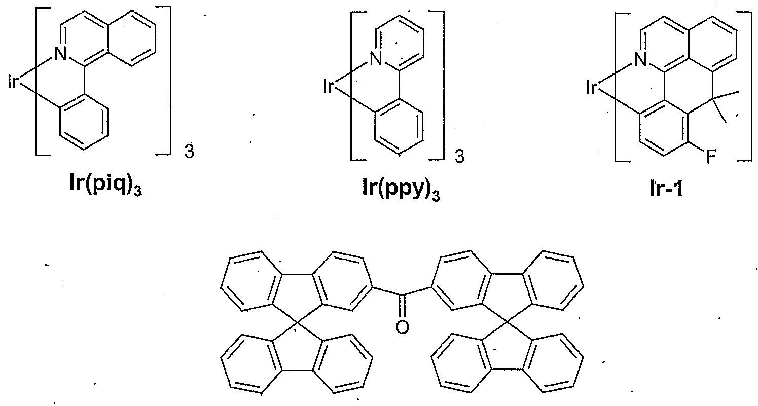
Tabelle 1:Table 1:

Zusammenfassend kann gesagt werden, dass OLEDs, gefertigt nach dem neuen Designprinzip, eine vergleichbare oder höhere Effizienz bei vergleichbaren Spannungen und vergleichbarer Lebensdauer aufweisen, wie man leicht aus Tabelle 1 entnehmen kann, wobei sich der Aufbau der OLED erheblich vereinfacht hat. ' In summary, it can be said that OLEDs, manufactured according to the new design principle, have a comparable or higher efficiency with comparable voltages and a comparable service life, as can easily be seen from Table 1, the structure of the OLED having been considerably simplified. '
Claims
Priority Applications (5)
| Application Number | Priority Date | Filing Date | Title |
|---|---|---|---|
| JP2006540366A JP2007512692A (en) | 2003-11-25 | 2004-11-24 | Organic electroluminescence device |
| CNB2004800348762A CN100536190C (en) | 2003-11-25 | 2004-11-24 | Organic electroluminescent element |
| KR1020067009445A KR101196683B1 (en) | 2003-11-25 | 2004-11-24 | Organic electroluminescent devices |
| US10/579,947 US7880379B2 (en) | 2003-11-25 | 2004-11-24 | Phosphorescent organic electroluminescent device having no hole transporting layer |
| EP04803246.0A EP1687859B1 (en) | 2003-11-25 | 2004-11-24 | Organic electroluminescent element |
Applications Claiming Priority (6)
| Application Number | Priority Date | Filing Date | Title |
|---|---|---|---|
| DE10355381.9 | 2003-11-25 | ||
| DE10355381A DE10355381A1 (en) | 2003-11-25 | 2003-11-25 | Organic electroluminescent device for semiconductors/organic LEDs has an anode, a cathode and a matrix layer with matrix material doped with a phosphorescent emitter |
| DE102004006622.1 | 2004-02-10 | ||
| DE102004006622A DE102004006622A1 (en) | 2004-02-10 | 2004-02-10 | Organic electroluminescent element, e.g. organic solar cell or organic laser diode for use in displays, has emission layer immediately adjacent to electrically conductive layer on anode side |
| DE102004015933.5 | 2004-04-01 | ||
| DE102004015933A DE102004015933A1 (en) | 2004-04-01 | 2004-04-01 | Organic electroluminescent element, e.g. organic solar cell or organic laser diode for use in displays, has emission layer immediately adjacent to electrically conductive layer on anode side |
Publications (1)
| Publication Number | Publication Date |
|---|---|
| WO2005053051A1 true WO2005053051A1 (en) | 2005-06-09 |
Family
ID=34636826
Family Applications (1)
| Application Number | Title | Priority Date | Filing Date |
|---|---|---|---|
| PCT/EP2004/013315 Ceased WO2005053051A1 (en) | 2003-11-25 | 2004-11-24 | Organic electroluminescent element |
Country Status (6)
| Country | Link |
|---|---|
| US (1) | US7880379B2 (en) |
| EP (1) | EP1687859B1 (en) |
| JP (1) | JP2007512692A (en) |
| KR (1) | KR101196683B1 (en) |
| CN (1) | CN100536190C (en) |
| WO (1) | WO2005053051A1 (en) |
Cited By (134)
| Publication number | Priority date | Publication date | Assignee | Title |
|---|---|---|---|---|
| DE102009031021A1 (en) | 2009-06-30 | 2011-01-05 | Merck Patent Gmbh | Materials for organic electroluminescent devices |
| WO2011006574A1 (en) | 2009-07-14 | 2011-01-20 | Merck Patent Gmbh | Materials for organic electroluminescent devices |
| WO2011042107A2 (en) | 2009-10-08 | 2011-04-14 | Merck Patent Gmbh | Materials for organic electroluminescent devices |
| DE102009053382A1 (en) | 2009-11-14 | 2011-05-19 | Merck Patent Gmbh | Materials for electronic devices |
| WO2011060867A1 (en) | 2009-11-18 | 2011-05-26 | Merck Patent Gmbh | Nitrogen-containing condensed heterocyclic compounds for oleds |
| WO2011085781A1 (en) | 2010-01-16 | 2011-07-21 | Merck Patent Gmbh | Materials for organic electroluminescent devices |
| WO2011116865A1 (en) | 2010-03-25 | 2011-09-29 | Merck Patent Gmbh | Materials for organic electroluminescence devices |
| DE102010018321A1 (en) | 2010-04-27 | 2011-10-27 | Merck Patent Gmbh | Organic electroluminescent device |
| DE102010019306A1 (en) | 2010-05-04 | 2011-11-10 | Merck Patent Gmbh | Organic electroluminescent devices |
| DE102009022858A1 (en) | 2009-05-27 | 2011-12-15 | Merck Patent Gmbh | Organic electroluminescent devices |
| WO2011160758A1 (en) | 2010-06-24 | 2011-12-29 | Merck Patent Gmbh | Materials for organic electroluminescent devices |
| DE102010045405A1 (en) | 2010-09-15 | 2012-03-15 | Merck Patent Gmbh | Materials for organic electroluminescent devices |
| DE102010048608A1 (en) | 2010-10-15 | 2012-04-19 | Merck Patent Gmbh | Materials for organic electroluminescent devices |
| WO2012069121A1 (en) | 2010-11-24 | 2012-05-31 | Merck Patent Gmbh | Materials for organic electroluminescent devices |
| DE102010054316A1 (en) | 2010-12-13 | 2012-06-14 | Merck Patent Gmbh | Substituted tetraarylbenzenes |
| DE102012000064A1 (en) | 2011-01-21 | 2012-07-26 | Merck Patent Gmbh | New heterocyclic compound excluding 9,10-dioxa-4b-aza-9a-phospha-indeno(1,2-a)indene and 9,10-dioxa-4b-aza-indeno(1,2-a)indene, useful e.g. as matrix material for fluorescent or phosphorescent emitters of electronic devices |
| EP2482159A2 (en) | 2011-01-28 | 2012-08-01 | Honeywell International, Inc. | Methods and reconfigurable systems to optimize the performance of a condition based health maintenance system |
| WO2012107163A1 (en) | 2011-02-12 | 2012-08-16 | Merck Patent Gmbh | Substituted dibenzonaphthacene |
| DE102011010841A1 (en) | 2011-02-10 | 2012-08-16 | Merck Patent Gmbh | (1,3) -dioxane-5-one compounds |
| WO2012143080A2 (en) | 2011-04-18 | 2012-10-26 | Merck Patent Gmbh | Materials for organic electroluminescent devices |
| WO2012163465A1 (en) | 2011-06-03 | 2012-12-06 | Merck Patent Gmbh | Organic electroluminescence device |
| WO2013041176A1 (en) | 2011-09-21 | 2013-03-28 | Merck Patent Gmbh | Carbazole derivatives for organic electroluminescence devices |
| DE102011116165A1 (en) | 2011-10-14 | 2013-04-18 | Merck Patent Gmbh | Benzodioxepin-3-one compounds |
| WO2013056776A1 (en) | 2011-10-20 | 2013-04-25 | Merck Patent Gmbh | Materials for organic electroluminescent devices |
| WO2013064206A1 (en) | 2011-11-01 | 2013-05-10 | Merck Patent Gmbh | Organic electroluminescent device |
| DE102011121022A1 (en) | 2011-12-13 | 2013-06-13 | Merck Patent Gmbh | Organic sensitizers for up-conversion |
| WO2013083216A1 (en) | 2011-11-17 | 2013-06-13 | Merck Patent Gmbh | Spiro dihydroacridine derivatives and the use thereof as materials for organic electroluminescence devices |
| WO2013120577A1 (en) | 2012-02-14 | 2013-08-22 | Merck Patent Gmbh | Spirobifluorene compounds for organic electroluminescent devices |
| WO2013139431A1 (en) | 2012-03-23 | 2013-09-26 | Merck Patent Gmbh | 9,9'-spirobixanthene derivatives for electroluminescent devices |
| WO2014008967A2 (en) | 2012-07-10 | 2014-01-16 | Merck Patent Gmbh | Materials for organic electroluminescent devices |
| WO2014015931A1 (en) | 2012-07-23 | 2014-01-30 | Merck Patent Gmbh | Materials for organic electroluminescent devices |
| WO2014023388A1 (en) | 2012-08-10 | 2014-02-13 | Merck Patent Gmbh | Materials for organic electroluminescence devices |
| WO2014056567A1 (en) | 2012-10-11 | 2014-04-17 | Merck Patent Gmbh | Materials for organic electroluminescent devices |
| US8865321B2 (en) | 2008-11-11 | 2014-10-21 | Merck Patent Gmbh | Organic electroluminescent devices |
| WO2015086108A1 (en) | 2013-12-12 | 2015-06-18 | Merck Patent Gmbh | Materials for electronic devices |
| WO2015169412A1 (en) | 2014-05-05 | 2015-11-12 | Merck Patent Gmbh | Materials for organic light emitting devices |
| WO2015197156A1 (en) | 2014-06-25 | 2015-12-30 | Merck Patent Gmbh | Materials for organic electroluminescent devices |
| WO2016074755A1 (en) | 2014-11-11 | 2016-05-19 | Merck Patent Gmbh | Materials for organic electroluminescent devices |
| WO2016198144A1 (en) | 2015-06-10 | 2016-12-15 | Merck Patent Gmbh | Materials for organic electroluminescent devices |
| WO2017012687A1 (en) | 2015-07-22 | 2017-01-26 | Merck Patent Gmbh | Materials for organic electroluminescent devices |
| WO2017016630A1 (en) | 2015-07-30 | 2017-02-02 | Merck Patent Gmbh | Materials for organic electroluminescent devices |
| WO2017025166A1 (en) | 2015-08-13 | 2017-02-16 | Merck Patent Gmbh | Hexamethylindanes |
| WO2017071791A1 (en) | 2015-10-27 | 2017-05-04 | Merck Patent Gmbh | Materials for organic electroluminescent devices |
| WO2017148565A1 (en) | 2016-03-03 | 2017-09-08 | Merck Patent Gmbh | Materials for organic electroluminescence devices |
| WO2017157983A1 (en) | 2016-03-17 | 2017-09-21 | Merck Patent Gmbh | Compounds with spirobifluorene-structures |
| WO2017178311A1 (en) | 2016-04-11 | 2017-10-19 | Merck Patent Gmbh | Heterocyclic compounds comprising dibenzofuran and/or dibenzothiophene structures |
| WO2017186760A1 (en) | 2016-04-29 | 2017-11-02 | Merck Patent Gmbh | Materials for organic electroluminescent devices |
| WO2017207596A1 (en) | 2016-06-03 | 2017-12-07 | Merck Patent Gmbh | Materials for organic electroluminescent devices |
| WO2018050584A1 (en) | 2016-09-14 | 2018-03-22 | Merck Patent Gmbh | Compounds with spirobifluorene-structures |
| WO2018050583A1 (en) | 2016-09-14 | 2018-03-22 | Merck Patent Gmbh | Compounds with carbazole structures |
| WO2018060218A1 (en) | 2016-09-30 | 2018-04-05 | Merck Patent Gmbh | Carbazoles with diazadibenzofurane or diazadibenzothiophene structures |
| WO2018060307A1 (en) | 2016-09-30 | 2018-04-05 | Merck Patent Gmbh | Compounds with diazadibenzofurane or diazadibenzothiophene structures |
| WO2018087346A1 (en) | 2016-11-14 | 2018-05-17 | Merck Patent Gmbh | Compounds with an acceptor and a donor group |
| WO2018091435A1 (en) | 2016-11-17 | 2018-05-24 | Merck Patent Gmbh | Materials for organic electroluminescent devices |
| WO2018099846A1 (en) | 2016-11-30 | 2018-06-07 | Merck Patent Gmbh | Compounds having valerolactam structures |
| WO2018104194A1 (en) | 2016-12-05 | 2018-06-14 | Merck Patent Gmbh | Materials for organic electroluminescent devices |
| WO2018104195A1 (en) | 2016-12-05 | 2018-06-14 | Merck Patent Gmbh | Nitrogen-containing heterocycles for use in oleds |
| WO2018104193A1 (en) | 2016-12-05 | 2018-06-14 | Merck Patent Gmbh | Materials for organic electroluminescent devices |
| WO2018114883A1 (en) | 2016-12-22 | 2018-06-28 | Merck Patent Gmbh | Mixtures comprising at least two organofunctional compounds |
| WO2018127465A1 (en) | 2017-01-04 | 2018-07-12 | Merck Patent Gmbh | Materials for organic electroluminescent devices |
| WO2018138306A1 (en) | 2017-01-30 | 2018-08-02 | Merck Patent Gmbh | Materials for organic electroluminescent devices |
| WO2018138039A1 (en) | 2017-01-25 | 2018-08-02 | Merck Patent Gmbh | Carbazole derivatives |
| WO2018149769A1 (en) | 2017-02-14 | 2018-08-23 | Merck Patent Gmbh | Materials for organic electroluminescent devices |
| WO2018166932A1 (en) | 2017-03-13 | 2018-09-20 | Merck Patent Gmbh | Compounds with arylamine structures |
| WO2018166934A1 (en) | 2017-03-15 | 2018-09-20 | Merck Patent Gmbh | Materials for organic electroluminescent devices |
| WO2018206526A1 (en) | 2017-05-11 | 2018-11-15 | Merck Patent Gmbh | Organoboron complexes for organic electroluminescent devices |
| WO2018206537A1 (en) | 2017-05-11 | 2018-11-15 | Merck Patent Gmbh | Carbazole-based bodipys for organic electroluminescent devices |
| WO2018215318A1 (en) | 2017-05-22 | 2018-11-29 | Merck Patent Gmbh | Hexacyclic heteroaromatic compounds for electronic devices |
| WO2019052933A1 (en) | 2017-09-12 | 2019-03-21 | Merck Patent Gmbh | MATERIALS FOR ORGANIC ELECTROLUMINESCENT DEVICES |
| WO2019068679A1 (en) | 2017-10-06 | 2019-04-11 | Merck Patent Gmbh | Materials for organic electroluminescent devices |
| WO2019081391A1 (en) | 2017-10-24 | 2019-05-02 | Merck Patent Gmbh | MATERIALS FOR ORGANIC ELECTROLUMINESCENT DEVICES |
| WO2019121458A1 (en) | 2017-12-19 | 2019-06-27 | Merck Patent Gmbh | Heterocyclic compound for use in electronic devices |
| WO2019145316A1 (en) | 2018-01-25 | 2019-08-01 | Merck Patent Gmbh | Materials for organic electroluminescent devices |
| WO2019233904A1 (en) | 2018-06-07 | 2019-12-12 | Merck Patent Gmbh | Organic electroluminescence devices |
| WO2020011686A1 (en) | 2018-07-09 | 2020-01-16 | Merck Patent Gmbh | Materials for organic electroluminescent devices |
| WO2020016264A1 (en) | 2018-07-20 | 2020-01-23 | Merck Patent Gmbh | Materials for organic electroluminescent devices |
| WO2020064662A2 (en) | 2018-09-27 | 2020-04-02 | Merck Patent Gmbh | Method for producing sterically hindered, nitrogen-containing heteroaromatic compounds |
| WO2020064666A1 (en) | 2018-09-27 | 2020-04-02 | Merck Patent Gmbh | Compounds that can be used in an organic electronic device as active compounds |
| WO2020094542A1 (en) | 2018-11-06 | 2020-05-14 | Merck Patent Gmbh | 5,6-diphenyl-5,6-dihydro-dibenz[c,e][1,2]azaphosphorin and 6-phenyl-6h-dibenzo[c,e][1,2]thiazin-5,5-dioxide derivatives and similar compounds as organic electroluminescent materials for oleds |
| WO2020094539A1 (en) | 2018-11-05 | 2020-05-14 | Merck Patent Gmbh | Compounds that can be used in an organic electronic device |
| WO2020099307A1 (en) | 2018-11-15 | 2020-05-22 | Merck Patent Gmbh | Materials for organic electroluminescent devices |
| WO2020099349A1 (en) | 2018-11-14 | 2020-05-22 | Merck Patent Gmbh | Compounds that can be used for producing an organic electronic device |
| WO2020127165A1 (en) | 2018-12-19 | 2020-06-25 | Merck Patent Gmbh | Materials for organic electroluminescent devices |
| WO2020148243A1 (en) | 2019-01-16 | 2020-07-23 | Merck Patent Gmbh | Materials for organic electroluminescent devices |
| WO2021043755A1 (en) | 2019-09-03 | 2021-03-11 | Merck Patent Gmbh | Materials for organic electroluminescent devices |
| WO2021052924A1 (en) | 2019-09-16 | 2021-03-25 | Merck Patent Gmbh | Materials for organic electroluminescent devices |
| WO2021078831A1 (en) | 2019-10-25 | 2021-04-29 | Merck Patent Gmbh | Compounds that can be used in an organic electronic device |
| WO2021078710A1 (en) | 2019-10-22 | 2021-04-29 | Merck Patent Gmbh | Materials for organic electroluminescent devices |
| WO2021122538A1 (en) | 2019-12-18 | 2021-06-24 | Merck Patent Gmbh | Aromatic compounds for organic electroluminescent devices |
| WO2021122740A1 (en) | 2019-12-19 | 2021-06-24 | Merck Patent Gmbh | Polycyclic compounds for organic electroluminescent devices |
| WO2021151922A1 (en) | 2020-01-29 | 2021-08-05 | Merck Patent Gmbh | Benzimidazole derivatives |
| WO2021170522A1 (en) | 2020-02-25 | 2021-09-02 | Merck Patent Gmbh | Use of heterocyclic compounds in an organic electronic device |
| WO2021175706A1 (en) | 2020-03-02 | 2021-09-10 | Merck Patent Gmbh | Use of sulfone compounds in an organic electronic device |
| WO2021185712A1 (en) | 2020-03-17 | 2021-09-23 | Merck Patent Gmbh | Heteroaromatic compounds for organic electroluminescent devices |
| WO2021185829A1 (en) | 2020-03-17 | 2021-09-23 | Merck Patent Gmbh | Heterocyclic compounds for organic electroluminescent devices |
| WO2021191183A1 (en) | 2020-03-26 | 2021-09-30 | Merck Patent Gmbh | Cyclic compounds for organic electroluminescent devices |
| WO2021204646A1 (en) | 2020-04-06 | 2021-10-14 | Merck Patent Gmbh | Polycyclic compounds for organic electroluminescent devices |
| WO2021254984A1 (en) | 2020-06-18 | 2021-12-23 | Merck Patent Gmbh | Indenoazanaphthalenes |
| WO2022002772A1 (en) | 2020-06-29 | 2022-01-06 | Merck Patent Gmbh | Heteroaromatic compounds for organic electroluminescent devices |
| WO2022002771A1 (en) | 2020-06-29 | 2022-01-06 | Merck Patent Gmbh | Heterocyclic compounds for organic electroluminescent devices |
| WO2022069422A1 (en) | 2020-09-30 | 2022-04-07 | Merck Patent Gmbh | Compounds for structuring functional layers of organic electroluminescent devices |
| WO2022069421A1 (en) | 2020-09-30 | 2022-04-07 | Merck Patent Gmbh | Compounds that can be used for structuring functional layers of organic electroluminescent devices |
| WO2022079067A1 (en) | 2020-10-16 | 2022-04-21 | Merck Patent Gmbh | Compounds comprising heteroatoms for organic electroluminescent devices |
| WO2022079068A1 (en) | 2020-10-16 | 2022-04-21 | Merck Patent Gmbh | Heterocyclic compounds for organic electroluminescent devices |
| WO2022101171A1 (en) | 2020-11-10 | 2022-05-19 | Merck Patent Gmbh | Sulfurous compounds for organic electroluminescent devices |
| WO2022117473A1 (en) | 2020-12-02 | 2022-06-09 | Merck Patent Gmbh | Heterocyclic compounds for organic electroluminescent devices |
| WO2022129113A1 (en) | 2020-12-18 | 2022-06-23 | Merck Patent Gmbh | Nitrogenous heteroaromatic compounds for organic electroluminescent devices |
| WO2022129114A1 (en) | 2020-12-18 | 2022-06-23 | Merck Patent Gmbh | Nitrogenous compounds for organic electroluminescent devices |
| WO2022129116A1 (en) | 2020-12-18 | 2022-06-23 | Merck Patent Gmbh | Indolo[3.2.1-jk]carbazole-6-carbonitrile derivatives as blue fluorescent emitters for use in oleds |
| WO2022157343A1 (en) | 2021-01-25 | 2022-07-28 | Merck Patent Gmbh | Nitrogenous compounds for organic electroluminescent devices |
| WO2022184601A1 (en) | 2021-03-02 | 2022-09-09 | Merck Patent Gmbh | Compounds for organic electroluminescent devices |
| WO2022194799A1 (en) | 2021-03-18 | 2022-09-22 | Merck Patent Gmbh | Heteroaromatic compounds for organic electroluminescent devices |
| WO2022229234A1 (en) | 2021-04-30 | 2022-11-03 | Merck Patent Gmbh | Nitrogenous heterocyclic compounds for organic electroluminescent devices |
| WO2023041454A1 (en) | 2021-09-14 | 2023-03-23 | Merck Patent Gmbh | Boronic heterocyclic compounds for organic electroluminescent devices |
| WO2023072799A1 (en) | 2021-10-27 | 2023-05-04 | Merck Patent Gmbh | Boronic and nitrogenous heterocyclic compounds for organic electroluminescent devices |
| WO2023099543A1 (en) | 2021-11-30 | 2023-06-08 | Merck Patent Gmbh | Compounds having fluorene structures |
| WO2023117835A1 (en) | 2021-12-21 | 2023-06-29 | Merck Patent Gmbh | Electronic devices |
| WO2023117836A1 (en) | 2021-12-21 | 2023-06-29 | Merck Patent Gmbh | Electronic devices |
| EP4236652A2 (en) | 2015-07-29 | 2023-08-30 | Merck Patent GmbH | Materials for organic electroluminescent devices |
| WO2023161167A1 (en) | 2022-02-23 | 2023-08-31 | Merck Patent Gmbh | Nitrogenous heterocycles for organic electroluminescent devices |
| WO2023161168A1 (en) | 2022-02-23 | 2023-08-31 | Merck Patent Gmbh | Aromatic hetreocycles for organic electroluminescent devices |
| WO2023213837A1 (en) | 2022-05-06 | 2023-11-09 | Merck Patent Gmbh | Cyclic compounds for organic electroluminescent devices |
| WO2024061948A1 (en) | 2022-09-22 | 2024-03-28 | Merck Patent Gmbh | Nitrogen-containing hetreocycles for organic electroluminescent devices |
| WO2024061942A1 (en) | 2022-09-22 | 2024-03-28 | Merck Patent Gmbh | Nitrogen-containing compounds for organic electroluminescent devices |
| WO2024094592A2 (en) | 2022-11-01 | 2024-05-10 | Merck Patent Gmbh | Nitrogenous heterocycles for organic electroluminescent devices |
| WO2024149694A1 (en) | 2023-01-10 | 2024-07-18 | Merck Patent Gmbh | Nitrogenous heterocycles for organic electroluminescent devices |
| WO2024153568A1 (en) | 2023-01-17 | 2024-07-25 | Merck Patent Gmbh | Heterocycles for organic electroluminescent devices |
| WO2024184050A1 (en) | 2023-03-07 | 2024-09-12 | Merck Patent Gmbh | Cyclic nitrogen compounds for organic electroluminescent devices |
| WO2025003084A1 (en) | 2023-06-28 | 2025-01-02 | Merck Patent Gmbh | Dicyanoaryl compounds for organic electroluminescent devices |
| WO2025045935A1 (en) | 2023-08-31 | 2025-03-06 | Merck Patent Gmbh | Cyano group-containing aromatic compounds for organic electroluminescent devices |
| WO2025109056A1 (en) | 2023-11-24 | 2025-05-30 | Merck Patent Gmbh | Oxygen-containing heterocycles for organic electroluminescent devices |
| WO2025181097A1 (en) | 2024-02-29 | 2025-09-04 | Merck Patent Gmbh | Nitrogen-containing hetreocycles for organic electroluminescent devices |
| WO2025181124A1 (en) | 2024-03-01 | 2025-09-04 | Merck Patent Gmbh | Materials for organic electroluminescent devices |
| WO2025181044A1 (en) | 2024-02-29 | 2025-09-04 | Merck Patent Gmbh | Nitrogen-containing compounds for organic electroluminescent devices |
Families Citing this family (7)
| Publication number | Priority date | Publication date | Assignee | Title |
|---|---|---|---|---|
| DE102007023876A1 (en) | 2007-03-02 | 2008-09-04 | Osram Opto Semiconductors Gmbh | Electric organic component comprises substrate, former electrode, which has anode, former electrically semiconducting layer on former electrode, organic functional layer on former electrically semiconducting layer |
| WO2009087064A1 (en) * | 2008-01-04 | 2009-07-16 | Basf Se | Electroluminescent ionic host-guest dendritic materials |
| KR20100028168A (en) * | 2008-09-04 | 2010-03-12 | 다우어드밴스드디스플레이머티리얼 유한회사 | Novel organic electroluminescent compounds and organic electroluminescent device using the same |
| US9236578B2 (en) | 2010-07-30 | 2016-01-12 | Merck Patent Gmbh | Organic electroluminescent device |
| CN102156098B (en) * | 2011-01-20 | 2012-08-29 | 安徽大学 | Vehicle-mounted solar spectrum collecting system |
| KR20120119449A (en) * | 2011-04-21 | 2012-10-31 | 삼성디스플레이 주식회사 | Organic light emitting diode display |
| KR101738727B1 (en) * | 2011-06-21 | 2017-05-22 | 카티바, 인크. | Materials and methods for oled microcavities and buffer layers |
Citations (5)
| Publication number | Priority date | Publication date | Assignee | Title |
|---|---|---|---|---|
| US20020028349A1 (en) * | 2000-08-22 | 2002-03-07 | Semiconductor Energy Laboratory Co., Ltd. | Light emitting device |
| WO2003001569A2 (en) * | 2001-06-21 | 2003-01-03 | The Trustees Of Princeton University | Organic light-emitting devices with blocking and transport layers |
| US20030096138A1 (en) * | 2001-11-07 | 2003-05-22 | Lecloux Daniel David | Electroluminescent iridium compounds having red-orange or red emission and devices made with such compounds |
| WO2003072681A1 (en) * | 2002-02-28 | 2003-09-04 | Jsr Corporation | Phosphors, process for production thereof, phosphorescent compositions and articles made by using the same |
| WO2004016709A1 (en) * | 2002-08-16 | 2004-02-26 | Neoviewkolon Co., Ltd. | Luminescent spiro-dimer and organic light-emitting device comprising the same |
Family Cites Families (39)
| Publication number | Priority date | Publication date | Assignee | Title |
|---|---|---|---|---|
| US4539507A (en) | 1983-03-25 | 1985-09-03 | Eastman Kodak Company | Organic electroluminescent devices having improved power conversion efficiencies |
| US5151629A (en) | 1991-08-01 | 1992-09-29 | Eastman Kodak Company | Blue emitting internal junction organic electroluminescent device (I) |
| US6048630A (en) | 1996-07-02 | 2000-04-11 | The Trustees Of Princeton University | Red-emitting organic light emitting devices (OLED's) |
| DE19738860A1 (en) | 1997-09-05 | 1999-03-11 | Hoechst Ag | Process for the preparation of aryl oligoamines |
| US6303238B1 (en) | 1997-12-01 | 2001-10-16 | The Trustees Of Princeton University | OLEDs doped with phosphorescent compounds |
| US6830828B2 (en) | 1998-09-14 | 2004-12-14 | The Trustees Of Princeton University | Organometallic complexes as phosphorescent emitters in organic LEDs |
| WO2000070655A2 (en) | 1999-05-13 | 2000-11-23 | The Trustees Of Princeton University | Very high efficiency organic light emitting devices based on electrophosphorescence |
| KR100946314B1 (en) | 1999-12-01 | 2010-03-09 | 더 트러스티즈 오브 프린스턴 유니버시티 | Organic light emitting device comprising a phosphorescent organo metallic compound |
| JP2002033191A (en) * | 2000-05-12 | 2002-01-31 | Semiconductor Energy Lab Co Ltd | Method for manufacturing light emitting device |
| US20020121638A1 (en) | 2000-06-30 | 2002-09-05 | Vladimir Grushin | Electroluminescent iridium compounds with fluorinated phenylpyridines, phenylpyrimidines, and phenylquinolines and devices made with such compounds |
| CN101924190B (en) | 2000-08-11 | 2012-07-04 | 普林斯顿大学理事会 | Organometallic compounds and emission-shifting organic electrophosphorescence |
| JP4154138B2 (en) | 2000-09-26 | 2008-09-24 | キヤノン株式会社 | Light emitting element, display device and metal coordination compound |
| JP4154139B2 (en) | 2000-09-26 | 2008-09-24 | キヤノン株式会社 | Light emitting element |
| JP4154140B2 (en) | 2000-09-26 | 2008-09-24 | キヤノン株式会社 | Metal coordination compounds |
| CN1285601C (en) | 2000-11-30 | 2006-11-22 | 佳能株式会社 | Light emitting devices and displays |
| DE10109027A1 (en) | 2001-02-24 | 2002-09-05 | Covion Organic Semiconductors | Rhodium and iridium complexes |
| DE10116962A1 (en) | 2001-04-05 | 2002-10-10 | Covion Organic Semiconductors | Rhodium and iridium complexes |
| EP1386953B1 (en) | 2001-04-13 | 2012-07-25 | Semiconductor Energy Laboratory Co., Ltd. | Organic light-emitting device and light-emitting apparatus comprising the device |
| CN1302565C (en) * | 2001-05-16 | 2007-02-28 | 普林斯顿大学理事会 | High Efficiency Multicolor Electrophosphorescent OLED |
| JP2003123980A (en) | 2001-10-12 | 2003-04-25 | Canon Inc | Organic light emitting device |
| TW519852B (en) * | 2001-10-18 | 2003-02-01 | Opto Tech Corp | Organic light emitting device capable of projecting white light source and its manufacturing method |
| US7166368B2 (en) | 2001-11-07 | 2007-01-23 | E. I. Du Pont De Nemours And Company | Electroluminescent platinum compounds and devices made with such compounds |
| DE10155064A1 (en) | 2001-11-09 | 2003-05-28 | Covion Organic Semiconductors | Rhodium and iridium complexes |
| US6734457B2 (en) | 2001-11-27 | 2004-05-11 | Semiconductor Energy Laboratory Co., Ltd. | Light emitting device |
| JP2003257676A (en) * | 2001-12-26 | 2003-09-12 | Fuji Photo Film Co Ltd | Organic electroluminescence element having layer containing conductive highpolymer |
| JP3965063B2 (en) * | 2002-03-08 | 2007-08-22 | Tdk株式会社 | Organic electroluminescence device |
| DE10215010A1 (en) | 2002-04-05 | 2003-10-23 | Covion Organic Semiconductors | Rhodium and iridium complexes |
| JP2003317946A (en) | 2002-04-23 | 2003-11-07 | Konica Minolta Holdings Inc | Organic el element and manufacturing method for organic el element |
| JP4103442B2 (en) * | 2002-04-25 | 2008-06-18 | コニカミノルタホールディングス株式会社 | Organic electroluminescence element and display device |
| DE10223337A1 (en) | 2002-05-25 | 2003-12-04 | Covion Organic Semiconductors | Process for the production of high-purity, tris-orthometallized organo-iridium compounds |
| DE10238903A1 (en) | 2002-08-24 | 2004-03-04 | Covion Organic Semiconductors Gmbh | New heteroaromatic rhodium and iridium complexes, useful in electroluminescent and/or phosphorescent devices as the emission layer and for use in solar cells, photovoltaic devices and organic photodetectors |
| DE10310887A1 (en) | 2003-03-11 | 2004-09-30 | Covion Organic Semiconductors Gmbh | Matallkomplexe |
| JP5318347B2 (en) | 2003-04-15 | 2013-10-16 | メルク パテント ゲーエムベーハー | Mixture of matrix material and organic semiconductor capable of emitting light, use thereof, and electronic component comprising said mixture |
| DE10355358A1 (en) | 2003-11-25 | 2005-07-07 | Covion Organic Semiconductors Gmbh | Mixtures for use in organic electronic devices of simplified layer structure comprise matrix materials (some of which in e.g. (hetero)aromatic ketone form are new) and emitters containing an element of atomic number above 20 |
| US7071614B2 (en) * | 2003-06-30 | 2006-07-04 | Organic Lighting Technologies Llc | Electron and hole modulating electrodes in organic light emitting diodes |
| DE10355380A1 (en) | 2003-11-25 | 2005-06-30 | Covion Organic Semiconductors Gmbh | New organometallic compounds are useful for the production of electronic components, organic light emitting diodes, organic integrated circuits and organic field effect transistors |
| DE10330761A1 (en) | 2003-07-07 | 2005-02-03 | Covion Organic Semiconductors Gmbh | New organometallic compounds are useful for the production of electronic components, organic light emitting diodes, organic integrated circuits and organic field effect transistors |
| DE10345572A1 (en) | 2003-09-29 | 2005-05-19 | Covion Organic Semiconductors Gmbh | metal complexes |
| DE102007023876A1 (en) * | 2007-03-02 | 2008-09-04 | Osram Opto Semiconductors Gmbh | Electric organic component comprises substrate, former electrode, which has anode, former electrically semiconducting layer on former electrode, organic functional layer on former electrically semiconducting layer |
-
2004
- 2004-11-24 JP JP2006540366A patent/JP2007512692A/en active Pending
- 2004-11-24 KR KR1020067009445A patent/KR101196683B1/en not_active Expired - Fee Related
- 2004-11-24 US US10/579,947 patent/US7880379B2/en not_active Expired - Fee Related
- 2004-11-24 EP EP04803246.0A patent/EP1687859B1/en not_active Expired - Lifetime
- 2004-11-24 CN CNB2004800348762A patent/CN100536190C/en not_active Expired - Fee Related
- 2004-11-24 WO PCT/EP2004/013315 patent/WO2005053051A1/en not_active Ceased
Patent Citations (6)
| Publication number | Priority date | Publication date | Assignee | Title |
|---|---|---|---|---|
| US20020028349A1 (en) * | 2000-08-22 | 2002-03-07 | Semiconductor Energy Laboratory Co., Ltd. | Light emitting device |
| WO2003001569A2 (en) * | 2001-06-21 | 2003-01-03 | The Trustees Of Princeton University | Organic light-emitting devices with blocking and transport layers |
| US20030096138A1 (en) * | 2001-11-07 | 2003-05-22 | Lecloux Daniel David | Electroluminescent iridium compounds having red-orange or red emission and devices made with such compounds |
| WO2003072681A1 (en) * | 2002-02-28 | 2003-09-04 | Jsr Corporation | Phosphors, process for production thereof, phosphorescent compositions and articles made by using the same |
| US20040106006A1 (en) * | 2002-02-28 | 2004-06-03 | Yuichi Eriyama | Phosphors, process for production thereof, phosphorescent compositions and articles made by using the same |
| WO2004016709A1 (en) * | 2002-08-16 | 2004-02-26 | Neoviewkolon Co., Ltd. | Luminescent spiro-dimer and organic light-emitting device comprising the same |
Non-Patent Citations (4)
| Title |
|---|
| COCCHI M ET AL: "HIGHLY EFFICIENT ORGANIC ELECTROPHOSPHORESCENT LIGHT-EMITTING DIODES WITH A REDUCED QUANTUM EFFICIENCY ROLL OFF AT LARGE CURRENT DENSITIES", APPLIED PHYSICS LETTERS, AMERICAN INSTITUTE OF PHYSICS. NEW YORK, US, vol. 84, no. 7, 16 February 2004 (2004-02-16), pages 1052 - 1054, XP001197382, ISSN: 0003-6951 * |
| LI H ET AL: "ORGANIC LIGHT-EMITTING DEVICES BASED ON AROMATIC POLYIMIDE DOPED BY ELECTROPHOSPHORESCENT MATERIAL FAC TRIS(2-PHENYLPYRIDINE) IRIDIUM", SEMICONDUCTOR SCIENCE AND TECHNOLOGY, INSTITUTE OF PHYSICS. LONDON, GB, vol. 18, no. 4, April 2003 (2003-04-01), pages 278 - 283, XP001169967, ISSN: 0268-1242 * |
| SALBECK J ET AL: "Low molecular organic glasses for blue electroluminescence", SYNTHETIC METALS, ELSEVIER SEQUOIA, LAUSANNE, CH, vol. 91, 1997, pages 209 - 215, XP002277588, ISSN: 0379-6779 * |
| TOKITO S ET AL: "HIGH-EFFICIENCY PHOSPHORESCENT POLYMER LIGHT-EMITTING DEVICES", ORGANIC ELECTRONICS, ELSEVIER, AMSTERDAM, NL, vol. 4, no. 2/3, September 2003 (2003-09-01), pages 105 - 111, XP001177145, ISSN: 1566-1199 * |
Cited By (165)
| Publication number | Priority date | Publication date | Assignee | Title |
|---|---|---|---|---|
| US8865321B2 (en) | 2008-11-11 | 2014-10-21 | Merck Patent Gmbh | Organic electroluminescent devices |
| DE102009022858A1 (en) | 2009-05-27 | 2011-12-15 | Merck Patent Gmbh | Organic electroluminescent devices |
| WO2011000455A1 (en) | 2009-06-30 | 2011-01-06 | Merck Patent Gmbh | Materials for organic electroluminescence devices |
| DE102009031021A1 (en) | 2009-06-30 | 2011-01-05 | Merck Patent Gmbh | Materials for organic electroluminescent devices |
| WO2011006574A1 (en) | 2009-07-14 | 2011-01-20 | Merck Patent Gmbh | Materials for organic electroluminescent devices |
| DE102009032922A1 (en) | 2009-07-14 | 2011-01-20 | Merck Patent Gmbh | Materials for organic electroluminescent devices |
| DE102009032922B4 (en) | 2009-07-14 | 2024-04-25 | Merck Patent Gmbh | Materials for organic electroluminescent devices, processes for their preparation, their use and electronic device |
| WO2011042107A2 (en) | 2009-10-08 | 2011-04-14 | Merck Patent Gmbh | Materials for organic electroluminescent devices |
| DE102009048791A1 (en) | 2009-10-08 | 2011-04-14 | Merck Patent Gmbh | Materials for organic electroluminescent devices |
| DE102009053382A1 (en) | 2009-11-14 | 2011-05-19 | Merck Patent Gmbh | Materials for electronic devices |
| WO2011057706A2 (en) | 2009-11-14 | 2011-05-19 | Merck Patent Gmbh | Materials for electronic devices |
| WO2011060867A1 (en) | 2009-11-18 | 2011-05-26 | Merck Patent Gmbh | Nitrogen-containing condensed heterocyclic compounds for oleds |
| DE102009053836A1 (en) | 2009-11-18 | 2011-05-26 | Merck Patent Gmbh | Materials for organic electroluminescent devices |
| DE102010004803A1 (en) | 2010-01-16 | 2011-07-21 | Merck Patent GmbH, 64293 | Materials for organic electroluminescent devices |
| WO2011085781A1 (en) | 2010-01-16 | 2011-07-21 | Merck Patent Gmbh | Materials for organic electroluminescent devices |
| WO2011116865A1 (en) | 2010-03-25 | 2011-09-29 | Merck Patent Gmbh | Materials for organic electroluminescence devices |
| DE102010012738A1 (en) | 2010-03-25 | 2011-09-29 | Merck Patent Gmbh | Materials for organic electroluminescent devices |
| DE102010018321A1 (en) | 2010-04-27 | 2011-10-27 | Merck Patent Gmbh | Organic electroluminescent device |
| WO2011134577A1 (en) | 2010-04-27 | 2011-11-03 | Merck Patent Gmbh | Organic electroluminescent device |
| DE102010019306A1 (en) | 2010-05-04 | 2011-11-10 | Merck Patent Gmbh | Organic electroluminescent devices |
| WO2011137951A1 (en) | 2010-05-04 | 2011-11-10 | Merck Patent Gmbh | Organic electroluminescence devices |
| DE102010024897A1 (en) | 2010-06-24 | 2011-12-29 | Merck Patent Gmbh | Materials for organic electroluminescent devices |
| WO2011160758A1 (en) | 2010-06-24 | 2011-12-29 | Merck Patent Gmbh | Materials for organic electroluminescent devices |
| DE102010045405A1 (en) | 2010-09-15 | 2012-03-15 | Merck Patent Gmbh | Materials for organic electroluminescent devices |
| WO2012034627A1 (en) | 2010-09-15 | 2012-03-22 | Merck Patent Gmbh | Materials for organic electroluminescent devices |
| WO2012048781A1 (en) | 2010-10-15 | 2012-04-19 | Merck Patent Gmbh | Triphenylene-based materials for organic electroluminescent devices |
| DE102010048608A1 (en) | 2010-10-15 | 2012-04-19 | Merck Patent Gmbh | Materials for organic electroluminescent devices |
| WO2012069121A1 (en) | 2010-11-24 | 2012-05-31 | Merck Patent Gmbh | Materials for organic electroluminescent devices |
| WO2012079678A1 (en) | 2010-12-13 | 2012-06-21 | Merck Patent Gmbh | Substituted tetraarylbenzenes |
| DE102010054316A1 (en) | 2010-12-13 | 2012-06-14 | Merck Patent Gmbh | Substituted tetraarylbenzenes |
| DE102012000064A1 (en) | 2011-01-21 | 2012-07-26 | Merck Patent Gmbh | New heterocyclic compound excluding 9,10-dioxa-4b-aza-9a-phospha-indeno(1,2-a)indene and 9,10-dioxa-4b-aza-indeno(1,2-a)indene, useful e.g. as matrix material for fluorescent or phosphorescent emitters of electronic devices |
| EP2482159A2 (en) | 2011-01-28 | 2012-08-01 | Honeywell International, Inc. | Methods and reconfigurable systems to optimize the performance of a condition based health maintenance system |
| DE102011010841A1 (en) | 2011-02-10 | 2012-08-16 | Merck Patent Gmbh | (1,3) -dioxane-5-one compounds |
| WO2012107158A1 (en) | 2011-02-10 | 2012-08-16 | Merck Patent Gmbh | 1,3-dioxan-5-one compounds |
| WO2012107163A1 (en) | 2011-02-12 | 2012-08-16 | Merck Patent Gmbh | Substituted dibenzonaphthacene |
| DE102011011104A1 (en) | 2011-02-12 | 2012-08-16 | Merck Patent Gmbh | Substituted dibenzonaphthacenes |
| WO2012143080A2 (en) | 2011-04-18 | 2012-10-26 | Merck Patent Gmbh | Materials for organic electroluminescent devices |
| WO2012163465A1 (en) | 2011-06-03 | 2012-12-06 | Merck Patent Gmbh | Organic electroluminescence device |
| WO2013041176A1 (en) | 2011-09-21 | 2013-03-28 | Merck Patent Gmbh | Carbazole derivatives for organic electroluminescence devices |
| DE102011116165A1 (en) | 2011-10-14 | 2013-04-18 | Merck Patent Gmbh | Benzodioxepin-3-one compounds |
| WO2013056776A1 (en) | 2011-10-20 | 2013-04-25 | Merck Patent Gmbh | Materials for organic electroluminescent devices |
| WO2013064206A1 (en) | 2011-11-01 | 2013-05-10 | Merck Patent Gmbh | Organic electroluminescent device |
| WO2013083216A1 (en) | 2011-11-17 | 2013-06-13 | Merck Patent Gmbh | Spiro dihydroacridine derivatives and the use thereof as materials for organic electroluminescence devices |
| DE102011121022A1 (en) | 2011-12-13 | 2013-06-13 | Merck Patent Gmbh | Organic sensitizers for up-conversion |
| WO2013087162A1 (en) | 2011-12-13 | 2013-06-20 | Merck Patent Gmbh | Organic sensitizers for up-conversion |
| WO2013120577A1 (en) | 2012-02-14 | 2013-08-22 | Merck Patent Gmbh | Spirobifluorene compounds for organic electroluminescent devices |
| EP3235892A1 (en) | 2012-02-14 | 2017-10-25 | Merck Patent GmbH | Materials for organic electroluminescent devices |
| EP3101088A1 (en) | 2012-02-14 | 2016-12-07 | Merck Patent GmbH | Materials for organic electroluminescent devices |
| WO2013139431A1 (en) | 2012-03-23 | 2013-09-26 | Merck Patent Gmbh | 9,9'-spirobixanthene derivatives for electroluminescent devices |
| WO2014008967A2 (en) | 2012-07-10 | 2014-01-16 | Merck Patent Gmbh | Materials for organic electroluminescent devices |
| WO2014015931A1 (en) | 2012-07-23 | 2014-01-30 | Merck Patent Gmbh | Materials for organic electroluminescent devices |
| WO2014023388A1 (en) | 2012-08-10 | 2014-02-13 | Merck Patent Gmbh | Materials for organic electroluminescence devices |
| WO2014056567A1 (en) | 2012-10-11 | 2014-04-17 | Merck Patent Gmbh | Materials for organic electroluminescent devices |
| WO2015086108A1 (en) | 2013-12-12 | 2015-06-18 | Merck Patent Gmbh | Materials for electronic devices |
| WO2015169412A1 (en) | 2014-05-05 | 2015-11-12 | Merck Patent Gmbh | Materials for organic light emitting devices |
| WO2015197156A1 (en) | 2014-06-25 | 2015-12-30 | Merck Patent Gmbh | Materials for organic electroluminescent devices |
| WO2016074755A1 (en) | 2014-11-11 | 2016-05-19 | Merck Patent Gmbh | Materials for organic electroluminescent devices |
| WO2016198144A1 (en) | 2015-06-10 | 2016-12-15 | Merck Patent Gmbh | Materials for organic electroluminescent devices |
| WO2017012687A1 (en) | 2015-07-22 | 2017-01-26 | Merck Patent Gmbh | Materials for organic electroluminescent devices |
| EP4236652A2 (en) | 2015-07-29 | 2023-08-30 | Merck Patent GmbH | Materials for organic electroluminescent devices |
| EP4301110A2 (en) | 2015-07-30 | 2024-01-03 | Merck Patent GmbH | Materials for organic electroluminescent devices |
| WO2017016630A1 (en) | 2015-07-30 | 2017-02-02 | Merck Patent Gmbh | Materials for organic electroluminescent devices |
| WO2017025166A1 (en) | 2015-08-13 | 2017-02-16 | Merck Patent Gmbh | Hexamethylindanes |
| WO2017071791A1 (en) | 2015-10-27 | 2017-05-04 | Merck Patent Gmbh | Materials for organic electroluminescent devices |
| WO2017148564A1 (en) | 2016-03-03 | 2017-09-08 | Merck Patent Gmbh | Materials for organic electroluminescent devices |
| WO2017148565A1 (en) | 2016-03-03 | 2017-09-08 | Merck Patent Gmbh | Materials for organic electroluminescence devices |
| WO2017157983A1 (en) | 2016-03-17 | 2017-09-21 | Merck Patent Gmbh | Compounds with spirobifluorene-structures |
| WO2017178311A1 (en) | 2016-04-11 | 2017-10-19 | Merck Patent Gmbh | Heterocyclic compounds comprising dibenzofuran and/or dibenzothiophene structures |
| WO2017186760A1 (en) | 2016-04-29 | 2017-11-02 | Merck Patent Gmbh | Materials for organic electroluminescent devices |
| WO2017207596A1 (en) | 2016-06-03 | 2017-12-07 | Merck Patent Gmbh | Materials for organic electroluminescent devices |
| EP3978477A2 (en) | 2016-06-03 | 2022-04-06 | Merck Patent GmbH | Materials for organic electroluminescent devices |
| WO2018050584A1 (en) | 2016-09-14 | 2018-03-22 | Merck Patent Gmbh | Compounds with spirobifluorene-structures |
| WO2018050583A1 (en) | 2016-09-14 | 2018-03-22 | Merck Patent Gmbh | Compounds with carbazole structures |
| US11447464B2 (en) | 2016-09-14 | 2022-09-20 | Merck Patent Gmbh | Compounds with spirobifluorene-structures |
| WO2018060218A1 (en) | 2016-09-30 | 2018-04-05 | Merck Patent Gmbh | Carbazoles with diazadibenzofurane or diazadibenzothiophene structures |
| WO2018060307A1 (en) | 2016-09-30 | 2018-04-05 | Merck Patent Gmbh | Compounds with diazadibenzofurane or diazadibenzothiophene structures |
| EP4271163A2 (en) | 2016-11-14 | 2023-11-01 | Merck Patent GmbH | Compounds with an acceptor and a donor group |
| WO2018087346A1 (en) | 2016-11-14 | 2018-05-17 | Merck Patent Gmbh | Compounds with an acceptor and a donor group |
| WO2018091435A1 (en) | 2016-11-17 | 2018-05-24 | Merck Patent Gmbh | Materials for organic electroluminescent devices |
| WO2018099846A1 (en) | 2016-11-30 | 2018-06-07 | Merck Patent Gmbh | Compounds having valerolactam structures |
| WO2018104193A1 (en) | 2016-12-05 | 2018-06-14 | Merck Patent Gmbh | Materials for organic electroluminescent devices |
| WO2018104195A1 (en) | 2016-12-05 | 2018-06-14 | Merck Patent Gmbh | Nitrogen-containing heterocycles for use in oleds |
| WO2018104194A1 (en) | 2016-12-05 | 2018-06-14 | Merck Patent Gmbh | Materials for organic electroluminescent devices |
| EP3978491A1 (en) | 2016-12-05 | 2022-04-06 | Merck Patent GmbH | Nitrogen-containing heterocycles for use in oleds |
| WO2018114883A1 (en) | 2016-12-22 | 2018-06-28 | Merck Patent Gmbh | Mixtures comprising at least two organofunctional compounds |
| WO2018127465A1 (en) | 2017-01-04 | 2018-07-12 | Merck Patent Gmbh | Materials for organic electroluminescent devices |
| WO2018138039A1 (en) | 2017-01-25 | 2018-08-02 | Merck Patent Gmbh | Carbazole derivatives |
| WO2018138306A1 (en) | 2017-01-30 | 2018-08-02 | Merck Patent Gmbh | Materials for organic electroluminescent devices |
| WO2018149769A1 (en) | 2017-02-14 | 2018-08-23 | Merck Patent Gmbh | Materials for organic electroluminescent devices |
| WO2018166932A1 (en) | 2017-03-13 | 2018-09-20 | Merck Patent Gmbh | Compounds with arylamine structures |
| WO2018166934A1 (en) | 2017-03-15 | 2018-09-20 | Merck Patent Gmbh | Materials for organic electroluminescent devices |
| WO2018206537A1 (en) | 2017-05-11 | 2018-11-15 | Merck Patent Gmbh | Carbazole-based bodipys for organic electroluminescent devices |
| WO2018206526A1 (en) | 2017-05-11 | 2018-11-15 | Merck Patent Gmbh | Organoboron complexes for organic electroluminescent devices |
| WO2018215318A1 (en) | 2017-05-22 | 2018-11-29 | Merck Patent Gmbh | Hexacyclic heteroaromatic compounds for electronic devices |
| WO2019052933A1 (en) | 2017-09-12 | 2019-03-21 | Merck Patent Gmbh | MATERIALS FOR ORGANIC ELECTROLUMINESCENT DEVICES |
| WO2019068679A1 (en) | 2017-10-06 | 2019-04-11 | Merck Patent Gmbh | Materials for organic electroluminescent devices |
| WO2019081391A1 (en) | 2017-10-24 | 2019-05-02 | Merck Patent Gmbh | MATERIALS FOR ORGANIC ELECTROLUMINESCENT DEVICES |
| WO2019121458A1 (en) | 2017-12-19 | 2019-06-27 | Merck Patent Gmbh | Heterocyclic compound for use in electronic devices |
| WO2019145316A1 (en) | 2018-01-25 | 2019-08-01 | Merck Patent Gmbh | Materials for organic electroluminescent devices |
| WO2019233904A1 (en) | 2018-06-07 | 2019-12-12 | Merck Patent Gmbh | Organic electroluminescence devices |
| WO2020011686A1 (en) | 2018-07-09 | 2020-01-16 | Merck Patent Gmbh | Materials for organic electroluminescent devices |
| WO2020016264A1 (en) | 2018-07-20 | 2020-01-23 | Merck Patent Gmbh | Materials for organic electroluminescent devices |
| EP4190880A1 (en) | 2018-09-27 | 2023-06-07 | Merck Patent GmbH | Compounds usable as active compounds in an organic electronic device |
| EP4601449A2 (en) | 2018-09-27 | 2025-08-13 | Merck Patent GmbH | Compounds usable as active compounds in an organic electronic device |
| WO2020064666A1 (en) | 2018-09-27 | 2020-04-02 | Merck Patent Gmbh | Compounds that can be used in an organic electronic device as active compounds |
| WO2020064662A2 (en) | 2018-09-27 | 2020-04-02 | Merck Patent Gmbh | Method for producing sterically hindered, nitrogen-containing heteroaromatic compounds |
| WO2020094539A1 (en) | 2018-11-05 | 2020-05-14 | Merck Patent Gmbh | Compounds that can be used in an organic electronic device |
| WO2020094542A1 (en) | 2018-11-06 | 2020-05-14 | Merck Patent Gmbh | 5,6-diphenyl-5,6-dihydro-dibenz[c,e][1,2]azaphosphorin and 6-phenyl-6h-dibenzo[c,e][1,2]thiazin-5,5-dioxide derivatives and similar compounds as organic electroluminescent materials for oleds |
| WO2020099349A1 (en) | 2018-11-14 | 2020-05-22 | Merck Patent Gmbh | Compounds that can be used for producing an organic electronic device |
| CN113195500A (en) * | 2018-11-15 | 2021-07-30 | 默克专利有限公司 | Material for organic electroluminescent device |
| WO2020099307A1 (en) | 2018-11-15 | 2020-05-22 | Merck Patent Gmbh | Materials for organic electroluminescent devices |
| US12035625B2 (en) | 2018-11-15 | 2024-07-09 | Merck Patent Gmbh | Materials for organic electroluminescent devices |
| CN113195500B (en) * | 2018-11-15 | 2024-05-17 | 默克专利有限公司 | Material for organic electroluminescent device |
| WO2020127165A1 (en) | 2018-12-19 | 2020-06-25 | Merck Patent Gmbh | Materials for organic electroluminescent devices |
| WO2020148243A1 (en) | 2019-01-16 | 2020-07-23 | Merck Patent Gmbh | Materials for organic electroluminescent devices |
| WO2021043755A1 (en) | 2019-09-03 | 2021-03-11 | Merck Patent Gmbh | Materials for organic electroluminescent devices |
| WO2021052924A1 (en) | 2019-09-16 | 2021-03-25 | Merck Patent Gmbh | Materials for organic electroluminescent devices |
| WO2021078710A1 (en) | 2019-10-22 | 2021-04-29 | Merck Patent Gmbh | Materials for organic electroluminescent devices |
| WO2021078831A1 (en) | 2019-10-25 | 2021-04-29 | Merck Patent Gmbh | Compounds that can be used in an organic electronic device |
| WO2021122538A1 (en) | 2019-12-18 | 2021-06-24 | Merck Patent Gmbh | Aromatic compounds for organic electroluminescent devices |
| WO2021122740A1 (en) | 2019-12-19 | 2021-06-24 | Merck Patent Gmbh | Polycyclic compounds for organic electroluminescent devices |
| WO2021151922A1 (en) | 2020-01-29 | 2021-08-05 | Merck Patent Gmbh | Benzimidazole derivatives |
| WO2021170522A1 (en) | 2020-02-25 | 2021-09-02 | Merck Patent Gmbh | Use of heterocyclic compounds in an organic electronic device |
| WO2021175706A1 (en) | 2020-03-02 | 2021-09-10 | Merck Patent Gmbh | Use of sulfone compounds in an organic electronic device |
| WO2021185829A1 (en) | 2020-03-17 | 2021-09-23 | Merck Patent Gmbh | Heterocyclic compounds for organic electroluminescent devices |
| WO2021185712A1 (en) | 2020-03-17 | 2021-09-23 | Merck Patent Gmbh | Heteroaromatic compounds for organic electroluminescent devices |
| WO2021191183A1 (en) | 2020-03-26 | 2021-09-30 | Merck Patent Gmbh | Cyclic compounds for organic electroluminescent devices |
| WO2021204646A1 (en) | 2020-04-06 | 2021-10-14 | Merck Patent Gmbh | Polycyclic compounds for organic electroluminescent devices |
| WO2021254984A1 (en) | 2020-06-18 | 2021-12-23 | Merck Patent Gmbh | Indenoazanaphthalenes |
| WO2022002771A1 (en) | 2020-06-29 | 2022-01-06 | Merck Patent Gmbh | Heterocyclic compounds for organic electroluminescent devices |
| WO2022002772A1 (en) | 2020-06-29 | 2022-01-06 | Merck Patent Gmbh | Heteroaromatic compounds for organic electroluminescent devices |
| WO2022069421A1 (en) | 2020-09-30 | 2022-04-07 | Merck Patent Gmbh | Compounds that can be used for structuring functional layers of organic electroluminescent devices |
| WO2022069422A1 (en) | 2020-09-30 | 2022-04-07 | Merck Patent Gmbh | Compounds for structuring functional layers of organic electroluminescent devices |
| WO2022079067A1 (en) | 2020-10-16 | 2022-04-21 | Merck Patent Gmbh | Compounds comprising heteroatoms for organic electroluminescent devices |
| WO2022079068A1 (en) | 2020-10-16 | 2022-04-21 | Merck Patent Gmbh | Heterocyclic compounds for organic electroluminescent devices |
| WO2022101171A1 (en) | 2020-11-10 | 2022-05-19 | Merck Patent Gmbh | Sulfurous compounds for organic electroluminescent devices |
| WO2022117473A1 (en) | 2020-12-02 | 2022-06-09 | Merck Patent Gmbh | Heterocyclic compounds for organic electroluminescent devices |
| EP4676208A2 (en) | 2020-12-18 | 2026-01-07 | Merck Patent GmbH | Nitrogen-containing hetero-aromatics for organic electroluminescent devices |
| WO2022129114A1 (en) | 2020-12-18 | 2022-06-23 | Merck Patent Gmbh | Nitrogenous compounds for organic electroluminescent devices |
| WO2022129113A1 (en) | 2020-12-18 | 2022-06-23 | Merck Patent Gmbh | Nitrogenous heteroaromatic compounds for organic electroluminescent devices |
| WO2022129116A1 (en) | 2020-12-18 | 2022-06-23 | Merck Patent Gmbh | Indolo[3.2.1-jk]carbazole-6-carbonitrile derivatives as blue fluorescent emitters for use in oleds |
| WO2022157343A1 (en) | 2021-01-25 | 2022-07-28 | Merck Patent Gmbh | Nitrogenous compounds for organic electroluminescent devices |
| WO2022184601A1 (en) | 2021-03-02 | 2022-09-09 | Merck Patent Gmbh | Compounds for organic electroluminescent devices |
| WO2022194799A1 (en) | 2021-03-18 | 2022-09-22 | Merck Patent Gmbh | Heteroaromatic compounds for organic electroluminescent devices |
| WO2022229234A1 (en) | 2021-04-30 | 2022-11-03 | Merck Patent Gmbh | Nitrogenous heterocyclic compounds for organic electroluminescent devices |
| WO2023041454A1 (en) | 2021-09-14 | 2023-03-23 | Merck Patent Gmbh | Boronic heterocyclic compounds for organic electroluminescent devices |
| WO2023072799A1 (en) | 2021-10-27 | 2023-05-04 | Merck Patent Gmbh | Boronic and nitrogenous heterocyclic compounds for organic electroluminescent devices |
| WO2023099543A1 (en) | 2021-11-30 | 2023-06-08 | Merck Patent Gmbh | Compounds having fluorene structures |
| WO2023117836A1 (en) | 2021-12-21 | 2023-06-29 | Merck Patent Gmbh | Electronic devices |
| WO2023117835A1 (en) | 2021-12-21 | 2023-06-29 | Merck Patent Gmbh | Electronic devices |
| WO2023161167A1 (en) | 2022-02-23 | 2023-08-31 | Merck Patent Gmbh | Nitrogenous heterocycles for organic electroluminescent devices |
| WO2023161168A1 (en) | 2022-02-23 | 2023-08-31 | Merck Patent Gmbh | Aromatic hetreocycles for organic electroluminescent devices |
| WO2023213837A1 (en) | 2022-05-06 | 2023-11-09 | Merck Patent Gmbh | Cyclic compounds for organic electroluminescent devices |
| WO2024061942A1 (en) | 2022-09-22 | 2024-03-28 | Merck Patent Gmbh | Nitrogen-containing compounds for organic electroluminescent devices |
| WO2024061948A1 (en) | 2022-09-22 | 2024-03-28 | Merck Patent Gmbh | Nitrogen-containing hetreocycles for organic electroluminescent devices |
| WO2024094592A2 (en) | 2022-11-01 | 2024-05-10 | Merck Patent Gmbh | Nitrogenous heterocycles for organic electroluminescent devices |
| WO2024149694A1 (en) | 2023-01-10 | 2024-07-18 | Merck Patent Gmbh | Nitrogenous heterocycles for organic electroluminescent devices |
| WO2024153568A1 (en) | 2023-01-17 | 2024-07-25 | Merck Patent Gmbh | Heterocycles for organic electroluminescent devices |
| WO2024184050A1 (en) | 2023-03-07 | 2024-09-12 | Merck Patent Gmbh | Cyclic nitrogen compounds for organic electroluminescent devices |
| WO2025003084A1 (en) | 2023-06-28 | 2025-01-02 | Merck Patent Gmbh | Dicyanoaryl compounds for organic electroluminescent devices |
| WO2025045935A1 (en) | 2023-08-31 | 2025-03-06 | Merck Patent Gmbh | Cyano group-containing aromatic compounds for organic electroluminescent devices |
| WO2025109056A1 (en) | 2023-11-24 | 2025-05-30 | Merck Patent Gmbh | Oxygen-containing heterocycles for organic electroluminescent devices |
| WO2025181097A1 (en) | 2024-02-29 | 2025-09-04 | Merck Patent Gmbh | Nitrogen-containing hetreocycles for organic electroluminescent devices |
| WO2025181044A1 (en) | 2024-02-29 | 2025-09-04 | Merck Patent Gmbh | Nitrogen-containing compounds for organic electroluminescent devices |
| WO2025181124A1 (en) | 2024-03-01 | 2025-09-04 | Merck Patent Gmbh | Materials for organic electroluminescent devices |
Also Published As
| Publication number | Publication date |
|---|---|
| KR20060126469A (en) | 2006-12-07 |
| CN1898816A (en) | 2007-01-17 |
| US7880379B2 (en) | 2011-02-01 |
| EP1687859A1 (en) | 2006-08-09 |
| JP2007512692A (en) | 2007-05-17 |
| EP1687859B1 (en) | 2013-08-07 |
| US20070114915A1 (en) | 2007-05-24 |
| CN100536190C (en) | 2009-09-02 |
| KR101196683B1 (en) | 2012-11-06 |
Similar Documents
| Publication | Publication Date | Title |
|---|---|---|
| EP1687859B1 (en) | Organic electroluminescent element | |
| DE102012101652B4 (en) | Organic semiconducting material and electronic component | |
| EP2251396B1 (en) | Organic emission-capable materials and electronic components containing same | |
| EP1656706B1 (en) | Organic electroluminescent element | |
| EP1668718B1 (en) | Organic electroluminescent element | |
| DE60121950T2 (en) | ELECTROLUMINESCENTS IRIDIUM COMPOUNDS WITH FLUORINATED PHENYLPYRIDINES, PHENYLPYRIDINES AND PHENYLCHINOLINES AND SUCH CONNECTIVITY DEVICES | |
| DE102020104604A1 (en) | ORGANIC ELECTROLUMINESCENT MATERIALS AND DEVICES | |
| DE102010018511B4 (en) | Organic semiconducting material and electronic component | |
| WO2011134458A1 (en) | Organic semiconducting material and electronic component | |
| WO2010075836A2 (en) | Heterocyclic compounds and the use thereof in electronic and optoelectronic components | |
| WO2005053055A1 (en) | Organic electroluminescent element | |
| EP2229699B1 (en) | Dithiol transition metal complexes, and electronic or optoelectronic components | |
| EP3221294A1 (en) | Heterocyclic compounds for use in electronic devices | |
| EP3235020B1 (en) | Ambipolar host materials for optoelectronic elements | |
| EP1649731A1 (en) | Organic electroluminescent element | |
| WO2012136422A1 (en) | Optoelectronic component and use of a copper complex as dopant for doping a layer | |
| EP1697483B1 (en) | Organic electroluminescent element | |
| DE10330761A1 (en) | New organometallic compounds are useful for the production of electronic components, organic light emitting diodes, organic integrated circuits and organic field effect transistors | |
| DE10317556A1 (en) | Mixtures for use in organic electronic devices of simplified layer structure comprise matrix materials (some of which in e.g. (hetero)aromatic ketone form are new) and emitters containing an element of atomic number above 20 | |
| DE102018118278A1 (en) | Electronic device, display device, method of making the same and a connection | |
| DE102018125307A1 (en) | Organic light emitting device | |
| DE102008045663A1 (en) | Fluorine-bridged associates for opto-electronic applications | |
| WO2005078818A2 (en) | Phosphorescent electroluminescent element | |
| DE112023000085B4 (en) | Display panel | |
| DE102008058230B4 (en) | Quinoxaline compound, organic light emitting diode, organic thin film transistor and solar cell |
Legal Events
| Date | Code | Title | Description |
|---|---|---|---|
| WWE | Wipo information: entry into national phase |
Ref document number: 200480034876.2 Country of ref document: CN |
|
| AK | Designated states |
Kind code of ref document: A1 Designated state(s): AE AG AL AM AT AU AZ BA BB BG BR BW BY BZ CA CH CN CO CR CU CZ DE DK DM DZ EC EE EG ES FI GB GD GE GH GM HR HU ID IL IN IS JP KE KG KP KR KZ LC LK LR LS LT LU LV MA MD MG MK MN MW MX MZ NA NI NO NZ OM PG PH PL PT RO RU SC SD SE SG SK SL SY TJ TM TN TR TT TZ UA UG US UZ VC VN YU ZA ZM ZW |
|
| AL | Designated countries for regional patents |
Kind code of ref document: A1 Designated state(s): GM KE LS MW MZ NA SD SL SZ TZ UG ZM ZW AM AZ BY KG KZ MD RU TJ TM AT BE BG CH CY CZ DE DK EE ES FI FR GB GR HU IE IS IT LU MC NL PL PT RO SE SI SK TR BF BJ CF CG CI CM GA GN GQ GW ML MR NE SN TD TG |
|
| 121 | Ep: the epo has been informed by wipo that ep was designated in this application | ||
| WWE | Wipo information: entry into national phase |
Ref document number: 2004803246 Country of ref document: EP |
|
| WWE | Wipo information: entry into national phase |
Ref document number: 1020067009445 Country of ref document: KR |
|
| WWE | Wipo information: entry into national phase |
Ref document number: 2007114915 Country of ref document: US Ref document number: 10579947 Country of ref document: US |
|
| WWE | Wipo information: entry into national phase |
Ref document number: 2006540366 Country of ref document: JP |
|
| NENP | Non-entry into the national phase |
Ref country code: DE |
|
| WWW | Wipo information: withdrawn in national office |
Ref document number: DE |
|
| WWP | Wipo information: published in national office |
Ref document number: 2004803246 Country of ref document: EP |
|
| WWP | Wipo information: published in national office |
Ref document number: 1020067009445 Country of ref document: KR |
|
| WWP | Wipo information: published in national office |
Ref document number: 10579947 Country of ref document: US |