KR101842860B1 - 표시 장치의 구동 방법 - Google Patents
표시 장치의 구동 방법 Download PDFInfo
- Publication number
- KR101842860B1 KR101842860B1 KR1020127019214A KR20127019214A KR101842860B1 KR 101842860 B1 KR101842860 B1 KR 101842860B1 KR 1020127019214 A KR1020127019214 A KR 1020127019214A KR 20127019214 A KR20127019214 A KR 20127019214A KR 101842860 B1 KR101842860 B1 KR 101842860B1
- Authority
- KR
- South Korea
- Prior art keywords
- image
- display
- display device
- power source
- transistor
- Prior art date
- Legal status (The legal status is an assumption and is not a legal conclusion. Google has not performed a legal analysis and makes no representation as to the accuracy of the status listed.)
- Expired - Fee Related
Links
Images


Classifications
-
- G—PHYSICS
- G09—EDUCATION; CRYPTOGRAPHY; DISPLAY; ADVERTISING; SEALS
- G09G—ARRANGEMENTS OR CIRCUITS FOR CONTROL OF INDICATING DEVICES USING STATIC MEANS TO PRESENT VARIABLE INFORMATION
- G09G3/00—Control arrangements or circuits, of interest only in connection with visual indicators other than cathode-ray tubes
- G09G3/20—Control arrangements or circuits, of interest only in connection with visual indicators other than cathode-ray tubes for presentation of an assembly of a number of characters, e.g. a page, by composing the assembly by combination of individual elements arranged in a matrix no fixed position being assigned to or needed to be assigned to the individual characters or partial characters
- G09G3/34—Control arrangements or circuits, of interest only in connection with visual indicators other than cathode-ray tubes for presentation of an assembly of a number of characters, e.g. a page, by composing the assembly by combination of individual elements arranged in a matrix no fixed position being assigned to or needed to be assigned to the individual characters or partial characters by control of light from an independent source
- G09G3/36—Control arrangements or circuits, of interest only in connection with visual indicators other than cathode-ray tubes for presentation of an assembly of a number of characters, e.g. a page, by composing the assembly by combination of individual elements arranged in a matrix no fixed position being assigned to or needed to be assigned to the individual characters or partial characters by control of light from an independent source using liquid crystals
- G09G3/3611—Control of matrices with row and column drivers
- G09G3/3648—Control of matrices with row and column drivers using an active matrix
-
- G—PHYSICS
- G02—OPTICS
- G02F—OPTICAL DEVICES OR ARRANGEMENTS FOR THE CONTROL OF LIGHT BY MODIFICATION OF THE OPTICAL PROPERTIES OF THE MEDIA OF THE ELEMENTS INVOLVED THEREIN; NON-LINEAR OPTICS; FREQUENCY-CHANGING OF LIGHT; OPTICAL LOGIC ELEMENTS; OPTICAL ANALOGUE/DIGITAL CONVERTERS
- G02F1/00—Devices or arrangements for the control of the intensity, colour, phase, polarisation or direction of light arriving from an independent light source, e.g. switching, gating or modulating; Non-linear optics
- G02F1/01—Devices or arrangements for the control of the intensity, colour, phase, polarisation or direction of light arriving from an independent light source, e.g. switching, gating or modulating; Non-linear optics for the control of the intensity, phase, polarisation or colour
- G02F1/13—Devices or arrangements for the control of the intensity, colour, phase, polarisation or direction of light arriving from an independent light source, e.g. switching, gating or modulating; Non-linear optics for the control of the intensity, phase, polarisation or colour based on liquid crystals, e.g. single liquid crystal display cells
- G02F1/133—Constructional arrangements; Operation of liquid crystal cells; Circuit arrangements
- G02F1/13306—Circuit arrangements or driving methods for the control of single liquid crystal cells
-
- G—PHYSICS
- G09—EDUCATION; CRYPTOGRAPHY; DISPLAY; ADVERTISING; SEALS
- G09G—ARRANGEMENTS OR CIRCUITS FOR CONTROL OF INDICATING DEVICES USING STATIC MEANS TO PRESENT VARIABLE INFORMATION
- G09G3/00—Control arrangements or circuits, of interest only in connection with visual indicators other than cathode-ray tubes
- G09G3/20—Control arrangements or circuits, of interest only in connection with visual indicators other than cathode-ray tubes for presentation of an assembly of a number of characters, e.g. a page, by composing the assembly by combination of individual elements arranged in a matrix no fixed position being assigned to or needed to be assigned to the individual characters or partial characters
- G09G3/34—Control arrangements or circuits, of interest only in connection with visual indicators other than cathode-ray tubes for presentation of an assembly of a number of characters, e.g. a page, by composing the assembly by combination of individual elements arranged in a matrix no fixed position being assigned to or needed to be assigned to the individual characters or partial characters by control of light from an independent source
- G09G3/3406—Control of illumination source
- G09G3/3413—Details of control of colour illumination sources
-
- G—PHYSICS
- G02—OPTICS
- G02F—OPTICAL DEVICES OR ARRANGEMENTS FOR THE CONTROL OF LIGHT BY MODIFICATION OF THE OPTICAL PROPERTIES OF THE MEDIA OF THE ELEMENTS INVOLVED THEREIN; NON-LINEAR OPTICS; FREQUENCY-CHANGING OF LIGHT; OPTICAL LOGIC ELEMENTS; OPTICAL ANALOGUE/DIGITAL CONVERTERS
- G02F1/00—Devices or arrangements for the control of the intensity, colour, phase, polarisation or direction of light arriving from an independent light source, e.g. switching, gating or modulating; Non-linear optics
- G02F1/01—Devices or arrangements for the control of the intensity, colour, phase, polarisation or direction of light arriving from an independent light source, e.g. switching, gating or modulating; Non-linear optics for the control of the intensity, phase, polarisation or colour
- G02F1/13—Devices or arrangements for the control of the intensity, colour, phase, polarisation or direction of light arriving from an independent light source, e.g. switching, gating or modulating; Non-linear optics for the control of the intensity, phase, polarisation or colour based on liquid crystals, e.g. single liquid crystal display cells
- G02F1/133—Constructional arrangements; Operation of liquid crystal cells; Circuit arrangements
- G02F1/1333—Constructional arrangements; Manufacturing methods
- G02F1/1334—Constructional arrangements; Manufacturing methods based on polymer dispersed liquid crystals, e.g. microencapsulated liquid crystals
-
- G—PHYSICS
- G02—OPTICS
- G02F—OPTICAL DEVICES OR ARRANGEMENTS FOR THE CONTROL OF LIGHT BY MODIFICATION OF THE OPTICAL PROPERTIES OF THE MEDIA OF THE ELEMENTS INVOLVED THEREIN; NON-LINEAR OPTICS; FREQUENCY-CHANGING OF LIGHT; OPTICAL LOGIC ELEMENTS; OPTICAL ANALOGUE/DIGITAL CONVERTERS
- G02F1/00—Devices or arrangements for the control of the intensity, colour, phase, polarisation or direction of light arriving from an independent light source, e.g. switching, gating or modulating; Non-linear optics
- G02F1/01—Devices or arrangements for the control of the intensity, colour, phase, polarisation or direction of light arriving from an independent light source, e.g. switching, gating or modulating; Non-linear optics for the control of the intensity, phase, polarisation or colour
- G02F1/13—Devices or arrangements for the control of the intensity, colour, phase, polarisation or direction of light arriving from an independent light source, e.g. switching, gating or modulating; Non-linear optics for the control of the intensity, phase, polarisation or colour based on liquid crystals, e.g. single liquid crystal display cells
- G02F1/133—Constructional arrangements; Operation of liquid crystal cells; Circuit arrangements
- G02F1/1333—Constructional arrangements; Manufacturing methods
- G02F1/1343—Electrodes
- G02F1/134309—Electrodes characterised by their geometrical arrangement
- G02F1/134336—Matrix
-
- G—PHYSICS
- G02—OPTICS
- G02F—OPTICAL DEVICES OR ARRANGEMENTS FOR THE CONTROL OF LIGHT BY MODIFICATION OF THE OPTICAL PROPERTIES OF THE MEDIA OF THE ELEMENTS INVOLVED THEREIN; NON-LINEAR OPTICS; FREQUENCY-CHANGING OF LIGHT; OPTICAL LOGIC ELEMENTS; OPTICAL ANALOGUE/DIGITAL CONVERTERS
- G02F1/00—Devices or arrangements for the control of the intensity, colour, phase, polarisation or direction of light arriving from an independent light source, e.g. switching, gating or modulating; Non-linear optics
- G02F1/01—Devices or arrangements for the control of the intensity, colour, phase, polarisation or direction of light arriving from an independent light source, e.g. switching, gating or modulating; Non-linear optics for the control of the intensity, phase, polarisation or colour
- G02F1/13—Devices or arrangements for the control of the intensity, colour, phase, polarisation or direction of light arriving from an independent light source, e.g. switching, gating or modulating; Non-linear optics for the control of the intensity, phase, polarisation or colour based on liquid crystals, e.g. single liquid crystal display cells
- G02F1/133—Constructional arrangements; Operation of liquid crystal cells; Circuit arrangements
- G02F1/136—Liquid crystal cells structurally associated with a semi-conducting layer or substrate, e.g. cells forming part of an integrated circuit
- G02F1/1362—Active matrix addressed cells
- G02F1/136286—Wiring, e.g. gate line, drain line
-
- G—PHYSICS
- G02—OPTICS
- G02F—OPTICAL DEVICES OR ARRANGEMENTS FOR THE CONTROL OF LIGHT BY MODIFICATION OF THE OPTICAL PROPERTIES OF THE MEDIA OF THE ELEMENTS INVOLVED THEREIN; NON-LINEAR OPTICS; FREQUENCY-CHANGING OF LIGHT; OPTICAL LOGIC ELEMENTS; OPTICAL ANALOGUE/DIGITAL CONVERTERS
- G02F1/00—Devices or arrangements for the control of the intensity, colour, phase, polarisation or direction of light arriving from an independent light source, e.g. switching, gating or modulating; Non-linear optics
- G02F1/01—Devices or arrangements for the control of the intensity, colour, phase, polarisation or direction of light arriving from an independent light source, e.g. switching, gating or modulating; Non-linear optics for the control of the intensity, phase, polarisation or colour
- G02F1/13—Devices or arrangements for the control of the intensity, colour, phase, polarisation or direction of light arriving from an independent light source, e.g. switching, gating or modulating; Non-linear optics for the control of the intensity, phase, polarisation or colour based on liquid crystals, e.g. single liquid crystal display cells
- G02F1/133—Constructional arrangements; Operation of liquid crystal cells; Circuit arrangements
- G02F1/136—Liquid crystal cells structurally associated with a semi-conducting layer or substrate, e.g. cells forming part of an integrated circuit
- G02F1/1362—Active matrix addressed cells
- G02F1/1368—Active matrix addressed cells in which the switching element is a three-electrode device
-
- G—PHYSICS
- G02—OPTICS
- G02F—OPTICAL DEVICES OR ARRANGEMENTS FOR THE CONTROL OF LIGHT BY MODIFICATION OF THE OPTICAL PROPERTIES OF THE MEDIA OF THE ELEMENTS INVOLVED THEREIN; NON-LINEAR OPTICS; FREQUENCY-CHANGING OF LIGHT; OPTICAL LOGIC ELEMENTS; OPTICAL ANALOGUE/DIGITAL CONVERTERS
- G02F2201/00—Constructional arrangements not provided for in groups G02F1/00 - G02F7/00
- G02F2201/12—Constructional arrangements not provided for in groups G02F1/00 - G02F7/00 electrode
- G02F2201/121—Constructional arrangements not provided for in groups G02F1/00 - G02F7/00 electrode common or background
-
- G—PHYSICS
- G02—OPTICS
- G02F—OPTICAL DEVICES OR ARRANGEMENTS FOR THE CONTROL OF LIGHT BY MODIFICATION OF THE OPTICAL PROPERTIES OF THE MEDIA OF THE ELEMENTS INVOLVED THEREIN; NON-LINEAR OPTICS; FREQUENCY-CHANGING OF LIGHT; OPTICAL LOGIC ELEMENTS; OPTICAL ANALOGUE/DIGITAL CONVERTERS
- G02F2201/00—Constructional arrangements not provided for in groups G02F1/00 - G02F7/00
- G02F2201/12—Constructional arrangements not provided for in groups G02F1/00 - G02F7/00 electrode
- G02F2201/123—Constructional arrangements not provided for in groups G02F1/00 - G02F7/00 electrode pixel
-
- G—PHYSICS
- G09—EDUCATION; CRYPTOGRAPHY; DISPLAY; ADVERTISING; SEALS
- G09G—ARRANGEMENTS OR CIRCUITS FOR CONTROL OF INDICATING DEVICES USING STATIC MEANS TO PRESENT VARIABLE INFORMATION
- G09G2300/00—Aspects of the constitution of display devices
- G09G2300/04—Structural and physical details of display devices
- G09G2300/0421—Structural details of the set of electrodes
- G09G2300/0426—Layout of electrodes and connections
-
- G—PHYSICS
- G09—EDUCATION; CRYPTOGRAPHY; DISPLAY; ADVERTISING; SEALS
- G09G—ARRANGEMENTS OR CIRCUITS FOR CONTROL OF INDICATING DEVICES USING STATIC MEANS TO PRESENT VARIABLE INFORMATION
- G09G2310/00—Command of the display device
- G09G2310/02—Addressing, scanning or driving the display screen or processing steps related thereto
- G09G2310/0237—Switching ON and OFF the backlight within one frame
-
- G—PHYSICS
- G09—EDUCATION; CRYPTOGRAPHY; DISPLAY; ADVERTISING; SEALS
- G09G—ARRANGEMENTS OR CIRCUITS FOR CONTROL OF INDICATING DEVICES USING STATIC MEANS TO PRESENT VARIABLE INFORMATION
- G09G2310/00—Command of the display device
- G09G2310/08—Details of timing specific for flat panels, other than clock recovery
-
- G—PHYSICS
- G09—EDUCATION; CRYPTOGRAPHY; DISPLAY; ADVERTISING; SEALS
- G09G—ARRANGEMENTS OR CIRCUITS FOR CONTROL OF INDICATING DEVICES USING STATIC MEANS TO PRESENT VARIABLE INFORMATION
- G09G2320/00—Control of display operating conditions
- G09G2320/02—Improving the quality of display appearance
- G09G2320/0209—Crosstalk reduction, i.e. to reduce direct or indirect influences of signals directed to a certain pixel of the displayed image on other pixels of said image, inclusive of influences affecting pixels in different frames or fields or sub-images which constitute a same image, e.g. left and right images of a stereoscopic display
- G09G2320/0214—Crosstalk reduction, i.e. to reduce direct or indirect influences of signals directed to a certain pixel of the displayed image on other pixels of said image, inclusive of influences affecting pixels in different frames or fields or sub-images which constitute a same image, e.g. left and right images of a stereoscopic display with crosstalk due to leakage current of pixel switch in active matrix panels
-
- G—PHYSICS
- G09—EDUCATION; CRYPTOGRAPHY; DISPLAY; ADVERTISING; SEALS
- G09G—ARRANGEMENTS OR CIRCUITS FOR CONTROL OF INDICATING DEVICES USING STATIC MEANS TO PRESENT VARIABLE INFORMATION
- G09G2320/00—Control of display operating conditions
- G09G2320/02—Improving the quality of display appearance
- G09G2320/0261—Improving the quality of display appearance in the context of movement of objects on the screen or movement of the observer relative to the screen
-
- G—PHYSICS
- G09—EDUCATION; CRYPTOGRAPHY; DISPLAY; ADVERTISING; SEALS
- G09G—ARRANGEMENTS OR CIRCUITS FOR CONTROL OF INDICATING DEVICES USING STATIC MEANS TO PRESENT VARIABLE INFORMATION
- G09G2320/00—Control of display operating conditions
- G09G2320/10—Special adaptations of display systems for operation with variable images
- G09G2320/103—Detection of image changes, e.g. determination of an index representative of the image change
-
- G—PHYSICS
- G09—EDUCATION; CRYPTOGRAPHY; DISPLAY; ADVERTISING; SEALS
- G09G—ARRANGEMENTS OR CIRCUITS FOR CONTROL OF INDICATING DEVICES USING STATIC MEANS TO PRESENT VARIABLE INFORMATION
- G09G2330/00—Aspects of power supply; Aspects of display protection and defect management
- G09G2330/02—Details of power systems and of start or stop of display operation
- G09G2330/021—Power management, e.g. power saving
-
- G—PHYSICS
- G09—EDUCATION; CRYPTOGRAPHY; DISPLAY; ADVERTISING; SEALS
- G09G—ARRANGEMENTS OR CIRCUITS FOR CONTROL OF INDICATING DEVICES USING STATIC MEANS TO PRESENT VARIABLE INFORMATION
- G09G2330/00—Aspects of power supply; Aspects of display protection and defect management
- G09G2330/02—Details of power systems and of start or stop of display operation
- G09G2330/026—Arrangements or methods related to booting a display
Landscapes
- Physics & Mathematics (AREA)
- Engineering & Computer Science (AREA)
- General Physics & Mathematics (AREA)
- Computer Hardware Design (AREA)
- Theoretical Computer Science (AREA)
- Chemical & Material Sciences (AREA)
- Crystallography & Structural Chemistry (AREA)
- Nonlinear Science (AREA)
- Mathematical Physics (AREA)
- Optics & Photonics (AREA)
- Control Of Indicators Other Than Cathode Ray Tubes (AREA)
- Liquid Crystal Display Device Control (AREA)
- Liquid Crystal (AREA)
Abstract
Description
도 2는 표시 장치의 하나의 모드를 도시하는 도면.
도 3은 표시 장치의 하나의 모드를 도시하는 도면.
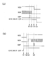
도 4는 표시 장치의 구동 방법의 하나의 모드를 도시하는 타이밍 차트.
도 5a 및 도 5b는 표시 장치의 구동 방법의 하나의 모드를 각각 도시하는 타이밍 차트.
도 6은 표시 장치의 구동 방법의 하나의 모드를 도시하는 도면.
도 7a 내지 도 7d는 표시 장치에 적용 가능한 트랜지스터의 하나의 모드를 각각 도시하는 도면.
도 8a 내지 도 8e는 표시 장치에 적용 가능한 트랜지스터를 제조하기 위한 방법의 하나의 모드를 도시하는 도면.
도 9a 및 도 9b는 전자 기기를 도시하는 도면.
도 10a 내지 도 10f는 전자 기기를 각각 도시하는 도면.
111: 메모리 회로 112: 비교기 회로
113: 표시 제어 회로 115: 선택 회로
120: 표시 패널 121: 구동 회로부
122: 화소부 123: 화소
124: 게이트선 125: 소스선
126: 단자부 127: 스위칭 소자
128: 공통 전극 130: 백라이트부
131: 백라이트 제어 회로 132: 백라이트
133: 발광 소자 203: 화소 회로부
210: 용량 소자 214: 트랜지스터
215: 표시 소자 400: 기판
401: 게이트 전극층 402: 게이트 절연층
403: 산화물 반도체층 407: 절연막
409: 보호 절연층 410: 트랜지스터
420: 트랜지스터 427: 절연층
430: 트랜지스터 437: 절연층
440: 트랜지스터 505: 기판
506: 보호 절연층 507: 게이트 절연층
510: 트랜지스터 511: 게이트 전극층
516: 절연층 530: 산화물 반도체막
531: 산화물 반도체층 601: 기간
602: 기간 603: 기간
604: 기간 111b: 프레임 메모리
121A: 게이트선 구동 회로 121B: 소스선 구동 회로
126A: 단자 126B: 단자
1401: 기간 1402: 기간
1403: 기간 1404: 기간
2700: 전자서적 리더 2701: 하우징
2703: 하우징 2705: 표시부
2707: 표시부 2711: 힌지
2721: 전원 2723: 조작키
2725: 스피커 2800: 하우징
2801: 하우징 2802: 표시 패널
2803: 스피커 2804: 마이크로폰
2805: 조작키 2806: 포인팅 디바이스
2807: 카메라 렌즈 2808: 외부 접속 단자
2810: 태양 전지셀 2811: 외부 메모리 슬롯
3001: 하우징 3002: 하우징
3003: 표시부 3004: 키보드
3021: 하우징 3022: 스타일러스
3023: 표시부 3024: 조작 버튼
3025: 외부 인터페이스 3051: 주 본체
3053: 접안부 3054: 조작 스위치
3055: 표시부 B 3056: 배터리
3057: 표시부 A 405a: 소스 전극층
405b: 드레인 전극층 436a: 배선층
436b: 배선층 515a: 소스 전극층
515b: 드레인 전극층 9600: 텔레비전 세트
9601: 하우징 9603: 표시부
9605: 스탠드 9630: 하우징
9631: 표시부 9632: 조작키
9633: 태양 전지 9634: 충방전 제어 회로
9635: 배터리 9636: 컨버터
9637: 컨버터
Claims (21)
- 표시 장치의 구동 방법에 있어서,
전원으로부터 전원 전위를 공급함으로써 화면 상에 화상을 표시하는 단계와;
상기 표시 장치에 초기화 화상 신호를 기록하는 단계와;
상기 화면 상에 초기화 화상을 표시하는 단계와;
상기 초기화 화상이 상기 화면 상에 표시된 상태로 상기 전원 전위의 공급을 정지하는 단계와;
상기 전원 전위의 공급을 정지하는 단계 후 미리 결정된 시간 동안 광원을 구동하는 단계와;
동시에 상기 광원의 구동을 정지하고 상기 초기화 화상의 표시를 정지하는 단계를 포함하는, 표시 장치의 구동 방법. - 삭제
- 삭제
- 표시 장치의 구동 방법에 있어서,
전원으로부터 전원 전위를 공급함으로써 화면 상에 화상을 표시하는 단계와;
상기 표시 장치에 보유 및 정지 신호를 공급하는 단계와;
상기 화상이 상기 화면 상에 표시된 상태로 상기 전원 전위의 공급을 정지하는 단계와;
상기 전원 전위의 공급을 정지하는 단계 후 미리 결정된 시간 동안 광원을 구동하는 단계와;
동시에 상기 광원의 구동을 정지하고 상기 화상의 표시를 정지하는 단계를 포함하는, 표시 장치의 구동 방법. - 삭제
- 삭제
- 삭제
- 표시 장치의 구동 방법에 있어서,
전원으로부터 전원 전위를 공급하고 전압을 표시 소자에 인가함으로써 화면 상에 화상을 표시하는 단계와;
상기 표시 장치에 초기화 화상 신호를 기록하는 단계와;
상기 화면 상에 초기화 화상을 표시하는 단계와;
상기 초기화 화상이 상기 표시 소자로의 상기 전압의 인가에 의해 상기 화면 상에 표시되는 동안 상기 전원 전위의 공급을 정지하는 단계와;
상기 전원 전위의 공급을 정지하는 단계 후 미리 결정된 시간 동안 광원을 구동하는 단계와;
동시에 상기 광원의 구동을 정지하고 상기 초기화 화상의 표시를 정지하는 단계를 포함하는, 표시 장치의 구동 방법. - 삭제
- 제 1 항 또는 제 8 항에 있어서,
상기 전원 전위의 공급이 정지된 후에 상기 초기화 화상이 표시되는 시간 기간은 상기 광원이 구동되는 시간 기간을 제어함으로써 설정되는, 표시 장치의 구동 방법. - 표시 장치의 구동 방법에 있어서,
전원으로부터 전원 전위를 공급하고 전압을 표시 소자에 인가함으로써 화면 상에 화상을 표시하는 단계와;
상기 표시 장치에 보유 및 정지 신호를 공급하는 단계와;
상기 화상이 상기 표시 소자로의 상기 전압의 인가에 의해 상기 화면 상에 표시되는 동안 상기 전원 전위의 공급을 정지하는 단계와;
상기 전원 전위의 공급을 정지하는 단계 후 미리 결정된 시간 동안 광원을 구동하는 단계와;
동시에 상기 광원의 구동을 정지하고 상기 화상의 표시를 정지하는 단계를 포함하는, 표시 장치의 구동 방법. - 제 1 항, 제 4 항, 제 8 항, 및 제 11 항 중 어느 한 항에 있어서,
상기 전원 전위를 공급하는 것은 산화물 반도체를 포함하는 트랜지스터에 의해 제어되는, 표시 장치의 구동 방법. - 제 4 항 또는 제 11 항에 있어서,
상기 전원 전위의 공급이 정지된 후에 상기 화상이 표시되는 시간 기간은 상기 광원이 구동되는 시간 기간을 제어함으로써 설정되는, 표시 장치의 구동 방법. - 삭제
- 표시 장치의 구동 방법에 있어서,
전원으로부터 트랜지스터를 통해 전원 전위를 공급하고 전압을 표시 소자에 인가함으로써 화면 상에 화상을 표시하는 단계와;
상기 표시 장치에 초기화 화상 신호를 기록하는 단계와;
상기 화면 상에 초기화 화상을 표시하는 단계와;
상기 표시 소자에 인가된 상기 전압의 보유에 의해 상기 초기화 화상이 상기 화면 상에 표시되는 동안 상기 표시 소자를 부유 상태가 되게 하기 위해 상기 트랜지스터를 턴오프하는 단계와;
상기 트랜지스터를 턴오프하는 단계 후 미리 결정된 시간 동안 광원을 구동하는 단계와;
동시에 상기 광원의 구동을 정지하고 상기 초기화 화상의 표시를 정지하는 단계를 포함하는, 표시 장치의 구동 방법. - 삭제
- 제 15 항에 있어서,
상기 트랜지스터가 턴오프된 후에 상기 초기화 화상이 표시되는 시간 기간은 상기 광원이 구동되는 시간 기간을 제어함으로써 설정되는, 표시 장치의 구동 방법. - 표시 장치의 구동 방법에 있어서,
전원으로부터 트랜지스터를 통해 전원 전위를 공급하고 전압을 표시 소자에 인가함으로써 화면 상에 화상을 표시하는 단계와;
상기 표시 장치에 보유 및 정지 신호를 공급하는 단계와;
상기 표시 소자에 인가된 상기 전압의 보유에 의해 상기 화상이 상기 화면 상에 표시되는 동안 상기 표시 소자를 부유 상태가 되게 하기 위해 상기 트랜지스터를 턴오프하는 단계와;
상기 트랜지스터를 턴오프하는 단계 후 미리 결정된 시간 동안 광원을 구동하는 단계와;
동시에 상기 광원의 구동을 정지하고 상기 화상의 표시를 정지하는 단계를 포함하는, 표시 장치의 구동 방법. - 제 15 항 또는 제 18 항에 있어서,
상기 트랜지스터는 산화물 반도체를 포함하는, 표시 장치의 구동 방법. - 제 18 항에 있어서,
상기 트랜지스터가 턴오프된 후에 상기 화상이 표시되는 시간 기간은 상기 광원이 구동되는 시간 기간을 제어함으로써 설정되는, 표시 장치의 구동 방법. - 제 4 항, 제 11 항, 및 제 18 항 중 어느 한 항에 있어서,
상기 전원 전위의 공급은 하나의 프레임의 화상 신호의 기록이 완료된 후에 정지되는, 표시 장치의 구동 방법.
Applications Claiming Priority (3)
| Application Number | Priority Date | Filing Date | Title |
|---|---|---|---|
| JP2010010321 | 2010-01-20 | ||
| JPJP-P-2010-010321 | 2010-01-20 | ||
| PCT/JP2010/073852 WO2011089843A1 (en) | 2010-01-20 | 2010-12-22 | Method for driving display device |
Publications (2)
| Publication Number | Publication Date |
|---|---|
| KR20120127424A KR20120127424A (ko) | 2012-11-21 |
| KR101842860B1 true KR101842860B1 (ko) | 2018-03-28 |
Family
ID=44277296
Family Applications (1)
| Application Number | Title | Priority Date | Filing Date |
|---|---|---|---|
| KR1020127019214A Expired - Fee Related KR101842860B1 (ko) | 2010-01-20 | 2010-12-22 | 표시 장치의 구동 방법 |
Country Status (5)
| Country | Link |
|---|---|
| US (3) | US9105251B2 (ko) |
| JP (3) | JP5723161B2 (ko) |
| KR (1) | KR101842860B1 (ko) |
| TW (3) | TWI637366B (ko) |
| WO (1) | WO2011089843A1 (ko) |
Families Citing this family (31)
| Publication number | Priority date | Publication date | Assignee | Title |
|---|---|---|---|---|
| JP5730529B2 (ja) | 2009-10-21 | 2015-06-10 | 株式会社半導体エネルギー研究所 | 半導体装置 |
| KR101842860B1 (ko) * | 2010-01-20 | 2018-03-28 | 가부시키가이샤 한도오따이 에네루기 켄큐쇼 | 표시 장치의 구동 방법 |
| KR101747421B1 (ko) * | 2010-01-20 | 2017-06-14 | 가부시키가이샤 한도오따이 에네루기 켄큐쇼 | 액정 표시 장치의 구동 방법 |
| KR101805378B1 (ko) | 2010-01-24 | 2017-12-06 | 가부시키가이샤 한도오따이 에네루기 켄큐쇼 | 표시 장치와 이의 제조 방법 |
| KR20200088506A (ko) | 2010-01-24 | 2020-07-22 | 가부시키가이샤 한도오따이 에네루기 켄큐쇼 | 표시 장치 |
| WO2011102248A1 (en) * | 2010-02-19 | 2011-08-25 | Semiconductor Energy Laboratory Co., Ltd. | Liquid crystal display device and electronic device |
| US10126803B1 (en) * | 2011-04-04 | 2018-11-13 | Google Llc | Conditional power management activities |
| US9355606B2 (en) * | 2012-01-31 | 2016-05-31 | Sharp Kabushiki Kaisha | Liquid crystal display device and liquid crystal display device driving method |
| JP5972914B2 (ja) * | 2012-01-31 | 2016-08-17 | シャープ株式会社 | 液晶表示装置、液晶表示装置の駆動方法 |
| CN106504697B (zh) | 2012-03-13 | 2019-11-26 | 株式会社半导体能源研究所 | 发光装置及其驱动方法 |
| US9601059B2 (en) * | 2012-05-15 | 2017-03-21 | Google Inc. | Dynamic backlight control selector |
| CN103809725B (zh) * | 2012-11-12 | 2017-03-29 | 联想(北京)有限公司 | 一种电子设备及基于该电子设备的状态切换方法 |
| WO2014077295A1 (en) | 2012-11-15 | 2014-05-22 | Semiconductor Energy Laboratory Co., Ltd. | Liquid crystal display device |
| WO2014080810A1 (ja) * | 2012-11-20 | 2014-05-30 | シャープ株式会社 | 液晶表示装置およびその駆動方法 |
| EP2924681B1 (en) * | 2012-11-22 | 2020-01-01 | Sharp Kabushiki Kaisha | Display device and electronic device |
| KR101448775B1 (ko) * | 2013-09-06 | 2014-10-08 | 현대자동차 주식회사 | 공조 패널 반도체 장치 및 이를 포함하는 차량용 공조 시스템 |
| US9806098B2 (en) | 2013-12-10 | 2017-10-31 | Semiconductor Energy Laboratory Co., Ltd. | Light-emitting device |
| KR102294280B1 (ko) * | 2014-03-05 | 2021-08-26 | 삼성전자주식회사 | 디스플레이 장치 및 이의 제어 방법 |
| US10022622B2 (en) | 2014-04-21 | 2018-07-17 | Steelseries Aps | Programmable actuation inputs of an accessory and methods thereof |
| JP6581825B2 (ja) * | 2014-07-18 | 2019-09-25 | 株式会社半導体エネルギー研究所 | 表示システム |
| TW201614626A (en) | 2014-09-05 | 2016-04-16 | Semiconductor Energy Lab | Display device and electronic device |
| KR20170091139A (ko) | 2014-12-01 | 2017-08-08 | 가부시키가이샤 한도오따이 에네루기 켄큐쇼 | 표시 장치, 상기 표시 장치를 갖는 표시 모듈, 및 상기 표시 장치 또는 상기 표시 모듈을 갖는 전자 기기 |
| CN105869576A (zh) * | 2015-01-24 | 2016-08-17 | 深圳富泰宏精密工业有限公司 | 提高显示稳定性的装置与方法 |
| DE102015219490A1 (de) * | 2015-10-08 | 2017-04-13 | BSH Hausgeräte GmbH | Matrixschaltung für eine Anzeigevorrichtung eines Haushaltsgerätes, Anzeigevorrichtung sowie Haushaltsgerät |
| US10504204B2 (en) * | 2016-07-13 | 2019-12-10 | Semiconductor Energy Laboratory Co., Ltd. | Electronic device |
| JP6903476B2 (ja) | 2017-04-20 | 2021-07-14 | 株式会社ジャパンディスプレイ | 表示装置 |
| US10712882B2 (en) * | 2018-02-09 | 2020-07-14 | Kabushiki Kaisha Tokai Rika Denki Seisakusho | Operational input device |
| CN108303832A (zh) * | 2018-02-13 | 2018-07-20 | 京东方科技集团股份有限公司 | 一种电子纸显示屏及其驱动方法、电子纸显示装置 |
| CN108761877A (zh) * | 2018-05-24 | 2018-11-06 | 京东方科技集团股份有限公司 | 显示面板、显示装置及基于其的控制方法 |
| US10935843B2 (en) * | 2019-02-08 | 2021-03-02 | Sharp Kabushiki Kaisha | Backlight and display device provided with same |
| CN110335570B (zh) * | 2019-05-08 | 2021-08-31 | 京东方科技集团股份有限公司 | 能耗控制方法、系统以及装置、计算机可读存储介质 |
Citations (6)
| Publication number | Priority date | Publication date | Assignee | Title |
|---|---|---|---|---|
| JP2000267066A (ja) | 1999-03-15 | 2000-09-29 | Canon Inc | 液晶素子 |
| JP2001249320A (ja) * | 2000-03-03 | 2001-09-14 | Alpine Electronics Inc | Lcd表示装置 |
| JP2004272270A (ja) * | 2003-03-11 | 2004-09-30 | Samsung Electronics Co Ltd | 液晶表示装置の駆動装置及びその方法 |
| JP2008309834A (ja) * | 2007-06-12 | 2008-12-25 | Seiko Epson Corp | 半導体集積回路、電源システムインタフェース及び電子機器 |
| JP2009151292A (ja) | 2007-11-29 | 2009-07-09 | Semiconductor Energy Lab Co Ltd | 表示装置およびその駆動方法 |
| JP2009229540A (ja) | 2008-03-19 | 2009-10-08 | Toshiba Corp | 液晶装置の駆動装置及び駆動方法 |
Family Cites Families (167)
| Publication number | Priority date | Publication date | Assignee | Title |
|---|---|---|---|---|
| JPS60198861A (ja) | 1984-03-23 | 1985-10-08 | Fujitsu Ltd | 薄膜トランジスタ |
| JPH0244256B2 (ja) | 1987-01-28 | 1990-10-03 | Kagaku Gijutsucho Mukizaishitsu Kenkyushocho | Ingazn2o5deshimesarerurotsuhoshokeinosojokozoojusurukagobutsuoyobisonoseizoho |
| JPH0244258B2 (ja) | 1987-02-24 | 1990-10-03 | Kagaku Gijutsucho Mukizaishitsu Kenkyushocho | Ingazn3o6deshimesarerurotsuhoshokeinosojokozoojusurukagobutsuoyobisonoseizoho |
| JPH0244260B2 (ja) | 1987-02-24 | 1990-10-03 | Kagaku Gijutsucho Mukizaishitsu Kenkyushocho | Ingazn5o8deshimesarerurotsuhoshokeinosojokozoojusurukagobutsuoyobisonoseizoho |
| JPS63210023A (ja) | 1987-02-24 | 1988-08-31 | Natl Inst For Res In Inorg Mater | InGaZn↓4O↓7で示される六方晶系の層状構造を有する化合物およびその製造法 |
| JPH0244262B2 (ja) | 1987-02-27 | 1990-10-03 | Kagaku Gijutsucho Mukizaishitsu Kenkyushocho | Ingazn6o9deshimesarerurotsuhoshokeinosojokozoojusurukagobutsuoyobisonoseizoho |
| JPH0244263B2 (ja) | 1987-04-22 | 1990-10-03 | Kagaku Gijutsucho Mukizaishitsu Kenkyushocho | Ingazn7o10deshimesarerurotsuhoshokeinosojokozoojusurukagobutsuoyobisonoseizoho |
| JPH01134497A (ja) * | 1987-11-20 | 1989-05-26 | Semiconductor Energy Lab Co Ltd | 液晶表示装置の電源回路 |
| KR940008180B1 (ko) * | 1990-12-27 | 1994-09-07 | 가부시끼가이샤 한도다이 에네르기 겐꾸쇼 | 액정 전기 광학 장치 및 그 구동 방법 |
| JPH05224626A (ja) * | 1992-02-14 | 1993-09-03 | Fujitsu Ltd | 液晶表示装置 |
| JPH05251705A (ja) | 1992-03-04 | 1993-09-28 | Fuji Xerox Co Ltd | 薄膜トランジスタ |
| JP3476241B2 (ja) * | 1994-02-25 | 2003-12-10 | 株式会社半導体エネルギー研究所 | アクティブマトリクス型表示装置の表示方法 |
| JPH07333577A (ja) | 1994-06-14 | 1995-12-22 | Matsushita Electric Ind Co Ltd | 液晶表示装置 |
| JP3479375B2 (ja) | 1995-03-27 | 2003-12-15 | 科学技術振興事業団 | 亜酸化銅等の金属酸化物半導体による薄膜トランジスタとpn接合を形成した金属酸化物半導体装置およびそれらの製造方法 |
| DE69635107D1 (de) | 1995-08-03 | 2005-09-29 | Koninkl Philips Electronics Nv | Halbleiteranordnung mit einem transparenten schaltungselement |
| JPH0990317A (ja) * | 1995-09-27 | 1997-04-04 | Canon Inc | 液晶ディスプレイ |
| US5959599A (en) | 1995-11-07 | 1999-09-28 | Semiconductor Energy Laboratory Co., Ltd. | Active matrix type liquid-crystal display unit and method of driving the same |
| JP3625598B2 (ja) * | 1995-12-30 | 2005-03-02 | 三星電子株式会社 | 液晶表示装置の製造方法 |
| TW455725B (en) | 1996-11-08 | 2001-09-21 | Seiko Epson Corp | Driver of liquid crystal panel, liquid crystal device, and electronic equipment |
| JP3827823B2 (ja) * | 1996-11-26 | 2006-09-27 | シャープ株式会社 | 液晶表示画像の消去装置及びそれを備えた液晶表示装置 |
| JP3496431B2 (ja) | 1997-02-03 | 2004-02-09 | カシオ計算機株式会社 | 表示装置及びその駆動方法 |
| JP3883641B2 (ja) | 1997-03-27 | 2007-02-21 | 株式会社半導体エネルギー研究所 | コンタクト構造およびアクティブマトリクス型表示装置 |
| JP3308880B2 (ja) | 1997-11-07 | 2002-07-29 | キヤノン株式会社 | 液晶表示装置と投写型液晶表示装置 |
| JP4170454B2 (ja) | 1998-07-24 | 2008-10-22 | Hoya株式会社 | 透明導電性酸化物薄膜を有する物品及びその製造方法 |
| JP2000150861A (ja) * | 1998-11-16 | 2000-05-30 | Tdk Corp | 酸化物薄膜 |
| JP3276930B2 (ja) * | 1998-11-17 | 2002-04-22 | 科学技術振興事業団 | トランジスタ及び半導体装置 |
| TW460731B (en) | 1999-09-03 | 2001-10-21 | Ind Tech Res Inst | Electrode structure and production method of wide viewing angle LCD |
| CN1198172C (zh) | 1999-12-03 | 2005-04-20 | 三菱电机株式会社 | 液晶显示装置 |
| TW494382B (en) * | 2000-03-22 | 2002-07-11 | Toshiba Corp | Display apparatus and driving method of display apparatus |
| JP2001272650A (ja) * | 2000-03-28 | 2001-10-05 | Matsushita Electric Ind Co Ltd | 液晶パネル駆動装置及び情報携帯機器 |
| JP2001290170A (ja) | 2000-04-04 | 2001-10-19 | Matsushita Electric Ind Co Ltd | 液晶表示装置とその駆動方法 |
| US7321353B2 (en) * | 2000-04-28 | 2008-01-22 | Sharp Kabushiki Kaisha | Display device method of driving same and electronic device mounting same |
| JP3766926B2 (ja) | 2000-04-28 | 2006-04-19 | シャープ株式会社 | 表示装置の駆動方法およびそれを用いた表示装置ならびに携帯機器 |
| JP2002026312A (ja) | 2000-07-06 | 2002-01-25 | National Institute Of Advanced Industrial & Technology | 半導体装置 |
| JP4089858B2 (ja) | 2000-09-01 | 2008-05-28 | 国立大学法人東北大学 | 半導体デバイス |
| TWI221595B (en) * | 2000-09-29 | 2004-10-01 | Sanyo Electric Co | Driving apparatus for display device |
| JP4995370B2 (ja) | 2000-10-25 | 2012-08-08 | 三菱電機株式会社 | 表示装置 |
| KR20020038482A (ko) * | 2000-11-15 | 2002-05-23 | 모리시타 요이찌 | 박막 트랜지스터 어레이, 그 제조방법 및 그것을 이용한표시패널 |
| JP2002169499A (ja) | 2000-11-30 | 2002-06-14 | Sanyo Electric Co Ltd | 表示パネルの駆動方法及び表示パネルの駆動制御装置 |
| JP3730159B2 (ja) | 2001-01-12 | 2005-12-21 | シャープ株式会社 | 表示装置の駆動方法および表示装置 |
| TW502525B (en) | 2001-02-02 | 2002-09-11 | Avision Inc | Scanner with reference pattern for combining pictures and the picture combining method |
| JP3997731B2 (ja) * | 2001-03-19 | 2007-10-24 | 富士ゼロックス株式会社 | 基材上に結晶性半導体薄膜を形成する方法 |
| JP2002289859A (ja) | 2001-03-23 | 2002-10-04 | Minolta Co Ltd | 薄膜トランジスタ |
| US6897843B2 (en) | 2001-07-14 | 2005-05-24 | Koninklijke Philips Electronics N.V. | Active matrix display devices |
| JP2003029721A (ja) * | 2001-07-17 | 2003-01-31 | Casio Comput Co Ltd | 液晶表示装置及びその表示駆動方法 |
| JP4090716B2 (ja) * | 2001-09-10 | 2008-05-28 | 雅司 川崎 | 薄膜トランジスタおよびマトリクス表示装置 |
| JP3925839B2 (ja) | 2001-09-10 | 2007-06-06 | シャープ株式会社 | 半導体記憶装置およびその試験方法 |
| JP2003131633A (ja) | 2001-10-29 | 2003-05-09 | Sony Corp | 表示装置の駆動方法 |
| JP4164562B2 (ja) | 2002-09-11 | 2008-10-15 | 独立行政法人科学技術振興機構 | ホモロガス薄膜を活性層として用いる透明薄膜電界効果型トランジスタ |
| WO2003040441A1 (fr) * | 2001-11-05 | 2003-05-15 | Japan Science And Technology Agency | Film mince monocristallin homologue a super-reseau naturel, procede de preparation et dispositif dans lequel est utilise ledit film mince monocristallin |
| JP4083486B2 (ja) * | 2002-02-21 | 2008-04-30 | 独立行政法人科学技術振興機構 | LnCuO(S,Se,Te)単結晶薄膜の製造方法 |
| JP4218249B2 (ja) | 2002-03-07 | 2009-02-04 | 株式会社日立製作所 | 表示装置 |
| CN1445821A (zh) * | 2002-03-15 | 2003-10-01 | 三洋电机株式会社 | ZnO膜和ZnO半导体层的形成方法、半导体元件及其制造方法 |
| JP3933591B2 (ja) * | 2002-03-26 | 2007-06-20 | 淳二 城戸 | 有機エレクトロルミネッセント素子 |
| JP4103425B2 (ja) | 2002-03-28 | 2008-06-18 | セイコーエプソン株式会社 | 電気光学装置、電子機器及び投射型表示装置 |
| US7339187B2 (en) | 2002-05-21 | 2008-03-04 | State Of Oregon Acting By And Through The Oregon State Board Of Higher Education On Behalf Of Oregon State University | Transistor structures |
| JP2004022625A (ja) * | 2002-06-13 | 2004-01-22 | Murata Mfg Co Ltd | 半導体デバイス及び該半導体デバイスの製造方法 |
| US7105868B2 (en) * | 2002-06-24 | 2006-09-12 | Cermet, Inc. | High-electron mobility transistor with zinc oxide |
| JP4638117B2 (ja) | 2002-08-22 | 2011-02-23 | シャープ株式会社 | 表示装置およびその駆動方法 |
| US7067843B2 (en) * | 2002-10-11 | 2006-06-27 | E. I. Du Pont De Nemours And Company | Transparent oxide semiconductor thin film transistors |
| JP4166105B2 (ja) | 2003-03-06 | 2008-10-15 | シャープ株式会社 | 半導体装置およびその製造方法 |
| JP2004273732A (ja) | 2003-03-07 | 2004-09-30 | Sharp Corp | アクティブマトリクス基板およびその製造方法 |
| US20040246280A1 (en) | 2003-06-06 | 2004-12-09 | Credelle Thomas Lloyd | Image degradation correction in novel liquid crystal displays |
| JP4108633B2 (ja) | 2003-06-20 | 2008-06-25 | シャープ株式会社 | 薄膜トランジスタおよびその製造方法ならびに電子デバイス |
| US7262463B2 (en) * | 2003-07-25 | 2007-08-28 | Hewlett-Packard Development Company, L.P. | Transistor including a deposited channel region having a doped portion |
| US7145174B2 (en) * | 2004-03-12 | 2006-12-05 | Hewlett-Packard Development Company, Lp. | Semiconductor device |
| CN102867855B (zh) | 2004-03-12 | 2015-07-15 | 独立行政法人科学技术振兴机构 | 薄膜晶体管及其制造方法 |
| US7297977B2 (en) | 2004-03-12 | 2007-11-20 | Hewlett-Packard Development Company, L.P. | Semiconductor device |
| US7282782B2 (en) * | 2004-03-12 | 2007-10-16 | Hewlett-Packard Development Company, L.P. | Combined binary oxide semiconductor device |
| JP2005300948A (ja) * | 2004-04-13 | 2005-10-27 | Hitachi Displays Ltd | 表示装置及びその駆動方法 |
| US7211825B2 (en) * | 2004-06-14 | 2007-05-01 | Yi-Chi Shih | Indium oxide-based thin film transistors and circuits |
| JP2006047500A (ja) | 2004-08-02 | 2006-02-16 | Seiko Epson Corp | 表示パネル駆動回路、表示装置及び電子機器 |
| JP2006100760A (ja) * | 2004-09-02 | 2006-04-13 | Casio Comput Co Ltd | 薄膜トランジスタおよびその製造方法 |
| US7285501B2 (en) * | 2004-09-17 | 2007-10-23 | Hewlett-Packard Development Company, L.P. | Method of forming a solution processed device |
| US7298084B2 (en) * | 2004-11-02 | 2007-11-20 | 3M Innovative Properties Company | Methods and displays utilizing integrated zinc oxide row and column drivers in conjunction with organic light emitting diodes |
| US7863611B2 (en) * | 2004-11-10 | 2011-01-04 | Canon Kabushiki Kaisha | Integrated circuits utilizing amorphous oxides |
| US7791072B2 (en) * | 2004-11-10 | 2010-09-07 | Canon Kabushiki Kaisha | Display |
| US7453065B2 (en) * | 2004-11-10 | 2008-11-18 | Canon Kabushiki Kaisha | Sensor and image pickup device |
| RU2358355C2 (ru) * | 2004-11-10 | 2009-06-10 | Кэнон Кабусики Кайся | Полевой транзистор |
| CN101057333B (zh) * | 2004-11-10 | 2011-11-16 | 佳能株式会社 | 发光器件 |
| CA2585190A1 (en) * | 2004-11-10 | 2006-05-18 | Canon Kabushiki Kaisha | Amorphous oxide and field effect transistor |
| JP5126729B2 (ja) | 2004-11-10 | 2013-01-23 | キヤノン株式会社 | 画像表示装置 |
| JP5118810B2 (ja) | 2004-11-10 | 2013-01-16 | キヤノン株式会社 | 電界効果型トランジスタ |
| US7829444B2 (en) * | 2004-11-10 | 2010-11-09 | Canon Kabushiki Kaisha | Field effect transistor manufacturing method |
| US7579224B2 (en) * | 2005-01-21 | 2009-08-25 | Semiconductor Energy Laboratory Co., Ltd. | Method for manufacturing a thin film semiconductor device |
| TWI505473B (zh) * | 2005-01-28 | 2015-10-21 | 半導體能源研究所股份有限公司 | 半導體裝置,電子裝置,和半導體裝置的製造方法 |
| TWI569441B (zh) * | 2005-01-28 | 2017-02-01 | 半導體能源研究所股份有限公司 | 半導體裝置,電子裝置,和半導體裝置的製造方法 |
| US7858451B2 (en) * | 2005-02-03 | 2010-12-28 | Semiconductor Energy Laboratory Co., Ltd. | Electronic device, semiconductor device and manufacturing method thereof |
| US7948171B2 (en) * | 2005-02-18 | 2011-05-24 | Semiconductor Energy Laboratory Co., Ltd. | Light emitting device |
| US20060197092A1 (en) * | 2005-03-03 | 2006-09-07 | Randy Hoffman | System and method for forming conductive material on a substrate |
| US8681077B2 (en) * | 2005-03-18 | 2014-03-25 | Semiconductor Energy Laboratory Co., Ltd. | Semiconductor device, and display device, driving method and electronic apparatus thereof |
| WO2006105077A2 (en) | 2005-03-28 | 2006-10-05 | Massachusetts Institute Of Technology | Low voltage thin film transistor with high-k dielectric material |
| US7645478B2 (en) | 2005-03-31 | 2010-01-12 | 3M Innovative Properties Company | Methods of making displays |
| US8300031B2 (en) | 2005-04-20 | 2012-10-30 | Semiconductor Energy Laboratory Co., Ltd. | Semiconductor device comprising transistor having gate and drain connected through a current-voltage conversion element |
| EP1724751B1 (en) | 2005-05-20 | 2013-04-10 | Semiconductor Energy Laboratory Co., Ltd. | Liquid crystal display device and electronic apparatus |
| JP4943058B2 (ja) | 2005-05-20 | 2012-05-30 | 株式会社半導体エネルギー研究所 | 液晶表示装置 |
| JP2006344849A (ja) | 2005-06-10 | 2006-12-21 | Casio Comput Co Ltd | 薄膜トランジスタ |
| US7691666B2 (en) | 2005-06-16 | 2010-04-06 | Eastman Kodak Company | Methods of making thin film transistors comprising zinc-oxide-based semiconductor materials and transistors made thereby |
| US7402506B2 (en) * | 2005-06-16 | 2008-07-22 | Eastman Kodak Company | Methods of making thin film transistors comprising zinc-oxide-based semiconductor materials and transistors made thereby |
| US7507618B2 (en) | 2005-06-27 | 2009-03-24 | 3M Innovative Properties Company | Method for making electronic devices using metal oxide nanoparticles |
| KR100711890B1 (ko) * | 2005-07-28 | 2007-04-25 | 삼성에스디아이 주식회사 | 유기 발광표시장치 및 그의 제조방법 |
| JP2007059128A (ja) * | 2005-08-23 | 2007-03-08 | Canon Inc | 有機el表示装置およびその製造方法 |
| JP4850457B2 (ja) | 2005-09-06 | 2012-01-11 | キヤノン株式会社 | 薄膜トランジスタ及び薄膜ダイオード |
| JP4560502B2 (ja) * | 2005-09-06 | 2010-10-13 | キヤノン株式会社 | 電界効果型トランジスタ |
| JP2007073705A (ja) * | 2005-09-06 | 2007-03-22 | Canon Inc | 酸化物半導体チャネル薄膜トランジスタおよびその製造方法 |
| JP5116225B2 (ja) * | 2005-09-06 | 2013-01-09 | キヤノン株式会社 | 酸化物半導体デバイスの製造方法 |
| JP4280736B2 (ja) * | 2005-09-06 | 2009-06-17 | キヤノン株式会社 | 半導体素子 |
| EP1998373A3 (en) * | 2005-09-29 | 2012-10-31 | Semiconductor Energy Laboratory Co, Ltd. | Semiconductor device having oxide semiconductor layer and manufacturing method thereof |
| JP5064747B2 (ja) | 2005-09-29 | 2012-10-31 | 株式会社半導体エネルギー研究所 | 半導体装置、電気泳動表示装置、表示モジュール、電子機器、及び半導体装置の作製方法 |
| JP5078246B2 (ja) | 2005-09-29 | 2012-11-21 | 株式会社半導体エネルギー研究所 | 半導体装置、及び半導体装置の作製方法 |
| JP5037808B2 (ja) * | 2005-10-20 | 2012-10-03 | キヤノン株式会社 | アモルファス酸化物を用いた電界効果型トランジスタ、及び該トランジスタを用いた表示装置 |
| US20060256133A1 (en) * | 2005-11-05 | 2006-11-16 | Outland Research | Gaze-responsive video advertisment display |
| KR20090130089A (ko) * | 2005-11-15 | 2009-12-17 | 가부시키가이샤 한도오따이 에네루기 켄큐쇼 | 다이오드 및 액티브 매트릭스 표시장치 |
| TWI292281B (en) * | 2005-12-29 | 2008-01-01 | Ind Tech Res Inst | Pixel structure of active organic light emitting diode and method of fabricating the same |
| US7867636B2 (en) * | 2006-01-11 | 2011-01-11 | Murata Manufacturing Co., Ltd. | Transparent conductive film and method for manufacturing the same |
| TW200728849A (en) | 2006-01-20 | 2007-08-01 | Niko Semiconductor Co Ltd | Backlight power supply device of liquid crystal display panel |
| JP4977478B2 (ja) * | 2006-01-21 | 2012-07-18 | 三星電子株式会社 | ZnOフィルム及びこれを用いたTFTの製造方法 |
| US7576394B2 (en) * | 2006-02-02 | 2009-08-18 | Kochi Industrial Promotion Center | Thin film transistor including low resistance conductive thin films and manufacturing method thereof |
| US7977169B2 (en) * | 2006-02-15 | 2011-07-12 | Kochi Industrial Promotion Center | Semiconductor device including active layer made of zinc oxide with controlled orientations and manufacturing method thereof |
| JP2007272203A (ja) | 2006-03-06 | 2007-10-18 | Nec Corp | 表示装置 |
| KR20070101595A (ko) | 2006-04-11 | 2007-10-17 | 삼성전자주식회사 | ZnO TFT |
| US20070252928A1 (en) | 2006-04-28 | 2007-11-01 | Toppan Printing Co., Ltd. | Structure, transmission type liquid crystal display, reflection type display and manufacturing method thereof |
| EP2025004A1 (en) | 2006-06-02 | 2009-02-18 | Kochi Industrial Promotion Center | Semiconductor device including an oxide semiconductor thin film layer of zinc oxide and manufacturing method thereof |
| JP5028033B2 (ja) | 2006-06-13 | 2012-09-19 | キヤノン株式会社 | 酸化物半導体膜のドライエッチング方法 |
| JP4999400B2 (ja) * | 2006-08-09 | 2012-08-15 | キヤノン株式会社 | 酸化物半導体膜のドライエッチング方法 |
| JP4609797B2 (ja) * | 2006-08-09 | 2011-01-12 | Nec液晶テクノロジー株式会社 | 薄膜デバイス及びその製造方法 |
| FR2905027B1 (fr) | 2006-08-21 | 2013-12-20 | Lg Philips Lcd Co Ltd | Dispositif d'affichage a cristaux liquides et son procede de pilotage |
| JP4332545B2 (ja) * | 2006-09-15 | 2009-09-16 | キヤノン株式会社 | 電界効果型トランジスタ及びその製造方法 |
| JP4415393B2 (ja) * | 2006-09-26 | 2010-02-17 | エプソンイメージングデバイス株式会社 | 駆動回路、液晶装置、電子機器、および液晶装置の駆動方法 |
| JP5164357B2 (ja) * | 2006-09-27 | 2013-03-21 | キヤノン株式会社 | 半導体装置及び半導体装置の製造方法 |
| JP4274219B2 (ja) * | 2006-09-27 | 2009-06-03 | セイコーエプソン株式会社 | 電子デバイス、有機エレクトロルミネッセンス装置、有機薄膜半導体装置 |
| US7622371B2 (en) * | 2006-10-10 | 2009-11-24 | Hewlett-Packard Development Company, L.P. | Fused nanocrystal thin film semiconductor and method |
| US7772021B2 (en) * | 2006-11-29 | 2010-08-10 | Samsung Electronics Co., Ltd. | Flat panel displays comprising a thin-film transistor having a semiconductive oxide in its channel and methods of fabricating the same for use in flat panel displays |
| JP2008140684A (ja) * | 2006-12-04 | 2008-06-19 | Toppan Printing Co Ltd | カラーelディスプレイおよびその製造方法 |
| KR101303578B1 (ko) * | 2007-01-05 | 2013-09-09 | 삼성전자주식회사 | 박막 식각 방법 |
| US8207063B2 (en) * | 2007-01-26 | 2012-06-26 | Eastman Kodak Company | Process for atomic layer deposition |
| KR100851215B1 (ko) * | 2007-03-14 | 2008-08-07 | 삼성에스디아이 주식회사 | 박막 트랜지스터 및 이를 이용한 유기 전계 발광표시장치 |
| US7795613B2 (en) | 2007-04-17 | 2010-09-14 | Toppan Printing Co., Ltd. | Structure with transistor |
| KR101325053B1 (ko) | 2007-04-18 | 2013-11-05 | 삼성디스플레이 주식회사 | 박막 트랜지스터 기판 및 이의 제조 방법 |
| KR20080094300A (ko) | 2007-04-19 | 2008-10-23 | 삼성전자주식회사 | 박막 트랜지스터 및 그 제조 방법과 박막 트랜지스터를포함하는 평판 디스플레이 |
| KR101334181B1 (ko) | 2007-04-20 | 2013-11-28 | 삼성전자주식회사 | 선택적으로 결정화된 채널층을 갖는 박막 트랜지스터 및 그제조 방법 |
| WO2008133345A1 (en) * | 2007-04-25 | 2008-11-06 | Canon Kabushiki Kaisha | Oxynitride semiconductor |
| US8325310B2 (en) | 2007-05-18 | 2012-12-04 | Semiconductor Energy Laboratory Co., Ltd. | Liquid crystal display device and manufacturing method thereof |
| KR101345376B1 (ko) | 2007-05-29 | 2013-12-24 | 삼성전자주식회사 | ZnO 계 박막 트랜지스터 및 그 제조방법 |
| JP2009042263A (ja) * | 2007-08-06 | 2009-02-26 | Seiko Epson Corp | 画像表示装置及びその制御方法 |
| US8102346B2 (en) | 2007-09-20 | 2012-01-24 | Sony Corporation | Electro-optical device and electronic apparatus including the same |
| JP2009099887A (ja) | 2007-10-19 | 2009-05-07 | Hitachi Displays Ltd | 表示装置 |
| JP5215158B2 (ja) * | 2007-12-17 | 2013-06-19 | 富士フイルム株式会社 | 無機結晶性配向膜及びその製造方法、半導体デバイス |
| JP2009162936A (ja) * | 2007-12-28 | 2009-07-23 | Rohm Co Ltd | ソースドライバ回路 |
| JP2009186542A (ja) * | 2008-02-04 | 2009-08-20 | Seiko Epson Corp | プロジェクタ |
| JP5325446B2 (ja) | 2008-04-16 | 2013-10-23 | 株式会社日立製作所 | 半導体装置及びその製造方法 |
| TWI413260B (zh) * | 2008-07-31 | 2013-10-21 | 半導體能源研究所股份有限公司 | 半導體裝置及其製造方法 |
| JP4623179B2 (ja) * | 2008-09-18 | 2011-02-02 | ソニー株式会社 | 薄膜トランジスタおよびその製造方法 |
| JP5451280B2 (ja) * | 2008-10-09 | 2014-03-26 | キヤノン株式会社 | ウルツ鉱型結晶成長用基板およびその製造方法ならびに半導体装置 |
| KR20180137606A (ko) | 2008-10-24 | 2018-12-27 | 가부시키가이샤 한도오따이 에네루기 켄큐쇼 | 반도체 장치 및 그 제조 방법 |
| US8450144B2 (en) * | 2009-03-26 | 2013-05-28 | Semiconductor Energy Laboratory Co., Ltd. | Semiconductor device and method for manufacturing the same |
| EP2489032B1 (en) * | 2009-10-16 | 2017-05-31 | Semiconductor Energy Laboratory Co. Ltd. | Liquid crystal display device and electronic apparatus having the same |
| KR101962603B1 (ko) * | 2009-10-16 | 2019-03-28 | 가부시키가이샤 한도오따이 에네루기 켄큐쇼 | 액정 표시 장치 및 액정 표시 장치를 포함한 전자 기기 |
| KR20120096463A (ko) * | 2009-10-21 | 2012-08-30 | 가부시키가이샤 한도오따이 에네루기 켄큐쇼 | 표시 장치 및 표시 장치를 갖는 전자 기기 |
| WO2011052344A1 (en) * | 2009-10-30 | 2011-05-05 | Semiconductor Energy Laboratory Co., Ltd. | Liquid crystal display device, driving method of the same, and electronic appliance including the same |
| KR20230173233A (ko) * | 2009-11-13 | 2023-12-26 | 가부시키가이샤 한도오따이 에네루기 켄큐쇼 | 표시 장치 및 이 표시 장치를 구비한 전자 기기 |
| KR101839931B1 (ko) * | 2009-11-30 | 2018-03-19 | 가부시키가이샤 한도오따이 에네루기 켄큐쇼 | 액정 표시 장치, 액정 표시 장치의 구동 방법, 및 이 액정 표시 장치를 구비하는 전자기기 |
| KR101840623B1 (ko) * | 2009-12-04 | 2018-03-21 | 가부시키가이샤 한도오따이 에네루기 켄큐쇼 | 표시 장치 및 이를 포함하는 전자 기기 |
| KR101761957B1 (ko) | 2009-12-18 | 2017-07-26 | 가부시키가이샤 한도오따이 에네루기 켄큐쇼 | 액정 표시 장치를 구동하는 방법 |
| KR101763660B1 (ko) * | 2009-12-18 | 2017-08-01 | 가부시키가이샤 한도오따이 에네루기 켄큐쇼 | 액정 표시 장치 및 그 구동 방법 |
| KR101747421B1 (ko) * | 2010-01-20 | 2017-06-14 | 가부시키가이샤 한도오따이 에네루기 켄큐쇼 | 액정 표시 장치의 구동 방법 |
| KR101842860B1 (ko) * | 2010-01-20 | 2018-03-28 | 가부시키가이샤 한도오따이 에네루기 켄큐쇼 | 표시 장치의 구동 방법 |
-
2010
- 2010-12-22 KR KR1020127019214A patent/KR101842860B1/ko not_active Expired - Fee Related
- 2010-12-22 WO PCT/JP2010/073852 patent/WO2011089843A1/en not_active Ceased
-
2011
- 2011-01-06 TW TW106100478A patent/TWI637366B/zh active
- 2011-01-06 TW TW100100482A patent/TWI522983B/zh active
- 2011-01-06 TW TW104141289A patent/TWI576805B/zh not_active IP Right Cessation
- 2011-01-13 US US13/005,558 patent/US9105251B2/en not_active Expired - Fee Related
- 2011-01-13 JP JP2011004930A patent/JP5723161B2/ja active Active
-
2015
- 2015-03-02 US US14/635,185 patent/US9454941B2/en active Active
- 2015-03-26 JP JP2015064439A patent/JP5883969B2/ja active Active
-
2016
- 2016-02-02 JP JP2016017917A patent/JP2016114954A/ja not_active Withdrawn
- 2016-09-22 US US15/272,530 patent/US9767748B2/en not_active Expired - Fee Related
Patent Citations (6)
| Publication number | Priority date | Publication date | Assignee | Title |
|---|---|---|---|---|
| JP2000267066A (ja) | 1999-03-15 | 2000-09-29 | Canon Inc | 液晶素子 |
| JP2001249320A (ja) * | 2000-03-03 | 2001-09-14 | Alpine Electronics Inc | Lcd表示装置 |
| JP2004272270A (ja) * | 2003-03-11 | 2004-09-30 | Samsung Electronics Co Ltd | 液晶表示装置の駆動装置及びその方法 |
| JP2008309834A (ja) * | 2007-06-12 | 2008-12-25 | Seiko Epson Corp | 半導体集積回路、電源システムインタフェース及び電子機器 |
| JP2009151292A (ja) | 2007-11-29 | 2009-07-09 | Semiconductor Energy Lab Co Ltd | 表示装置およびその駆動方法 |
| JP2009229540A (ja) | 2008-03-19 | 2009-10-08 | Toshiba Corp | 液晶装置の駆動装置及び駆動方法 |
Also Published As
| Publication number | Publication date |
|---|---|
| TWI576805B (zh) | 2017-04-01 |
| TW201717181A (zh) | 2017-05-16 |
| TW201137820A (en) | 2011-11-01 |
| US9767748B2 (en) | 2017-09-19 |
| US20110175894A1 (en) | 2011-07-21 |
| JP5723161B2 (ja) | 2015-05-27 |
| US9454941B2 (en) | 2016-09-27 |
| TWI637366B (zh) | 2018-10-01 |
| US9105251B2 (en) | 2015-08-11 |
| WO2011089843A1 (en) | 2011-07-28 |
| JP2015127835A (ja) | 2015-07-09 |
| JP5883969B2 (ja) | 2016-03-15 |
| JP2011170331A (ja) | 2011-09-01 |
| JP2016114954A (ja) | 2016-06-23 |
| US20170011698A1 (en) | 2017-01-12 |
| TWI522983B (zh) | 2016-02-21 |
| KR20120127424A (ko) | 2012-11-21 |
| US20150179119A1 (en) | 2015-06-25 |
| TW201610963A (zh) | 2016-03-16 |
Similar Documents
| Publication | Publication Date | Title |
|---|---|---|
| KR101842860B1 (ko) | 표시 장치의 구동 방법 | |
| JP7702463B2 (ja) | 液晶表示装置 |
Legal Events
| Date | Code | Title | Description |
|---|---|---|---|
| PA0105 | International application |
St.27 status event code: A-0-1-A10-A15-nap-PA0105 |
|
| PG1501 | Laying open of application |
St.27 status event code: A-1-1-Q10-Q12-nap-PG1501 |
|
| A201 | Request for examination | ||
| E13-X000 | Pre-grant limitation requested |
St.27 status event code: A-2-3-E10-E13-lim-X000 |
|
| P11-X000 | Amendment of application requested |
St.27 status event code: A-2-2-P10-P11-nap-X000 |
|
| P13-X000 | Application amended |
St.27 status event code: A-2-2-P10-P13-nap-X000 |
|
| PA0201 | Request for examination |
St.27 status event code: A-1-2-D10-D11-exm-PA0201 |
|
| P22-X000 | Classification modified |
St.27 status event code: A-2-2-P10-P22-nap-X000 |
|
| P22-X000 | Classification modified |
St.27 status event code: A-2-2-P10-P22-nap-X000 |
|
| D13-X000 | Search requested |
St.27 status event code: A-1-2-D10-D13-srh-X000 |
|
| D14-X000 | Search report completed |
St.27 status event code: A-1-2-D10-D14-srh-X000 |
|
| E902 | Notification of reason for refusal | ||
| PE0902 | Notice of grounds for rejection |
St.27 status event code: A-1-2-D10-D21-exm-PE0902 |
|
| P11-X000 | Amendment of application requested |
St.27 status event code: A-2-2-P10-P11-nap-X000 |
|
| P13-X000 | Application amended |
St.27 status event code: A-2-2-P10-P13-nap-X000 |
|
| E90F | Notification of reason for final refusal | ||
| PE0902 | Notice of grounds for rejection |
St.27 status event code: A-1-2-D10-D21-exm-PE0902 |
|
| P11-X000 | Amendment of application requested |
St.27 status event code: A-2-2-P10-P11-nap-X000 |
|
| P13-X000 | Application amended |
St.27 status event code: A-2-2-P10-P13-nap-X000 |
|
| E701 | Decision to grant or registration of patent right | ||
| PE0701 | Decision of registration |
St.27 status event code: A-1-2-D10-D22-exm-PE0701 |
|
| GRNT | Written decision to grant | ||
| PR0701 | Registration of establishment |
St.27 status event code: A-2-4-F10-F11-exm-PR0701 |
|
| PR1002 | Payment of registration fee |
St.27 status event code: A-2-2-U10-U12-oth-PR1002 Fee payment year number: 1 |
|
| PG1601 | Publication of registration |
St.27 status event code: A-4-4-Q10-Q13-nap-PG1601 |
|
| PC1903 | Unpaid annual fee |
St.27 status event code: A-4-4-U10-U13-oth-PC1903 Not in force date: 20210323 Payment event data comment text: Termination Category : DEFAULT_OF_REGISTRATION_FEE |
|
| PC1903 | Unpaid annual fee |
St.27 status event code: N-4-6-H10-H13-oth-PC1903 Ip right cessation event data comment text: Termination Category : DEFAULT_OF_REGISTRATION_FEE Not in force date: 20210323 |