JP7170606B2 - Dc-dcコンバータ - Google Patents
Dc-dcコンバータ Download PDFInfo
- Publication number
- JP7170606B2 JP7170606B2 JP2019160567A JP2019160567A JP7170606B2 JP 7170606 B2 JP7170606 B2 JP 7170606B2 JP 2019160567 A JP2019160567 A JP 2019160567A JP 2019160567 A JP2019160567 A JP 2019160567A JP 7170606 B2 JP7170606 B2 JP 7170606B2
- Authority
- JP
- Japan
- Prior art keywords
- signal
- output
- converter
- pulse width
- circuit
- Prior art date
- Legal status (The legal status is an assumption and is not a legal conclusion. Google has not performed a legal analysis and makes no representation as to the accuracy of the status listed.)
- Active
Links
Images


Classifications
-
- H—ELECTRICITY
- H02—GENERATION; CONVERSION OR DISTRIBUTION OF ELECTRIC POWER
- H02M—APPARATUS FOR CONVERSION BETWEEN AC AND AC, BETWEEN AC AND DC, OR BETWEEN DC AND DC, AND FOR USE WITH MAINS OR SIMILAR POWER SUPPLY SYSTEMS; CONVERSION OF DC OR AC INPUT POWER INTO SURGE OUTPUT POWER; CONTROL OR REGULATION THEREOF
- H02M3/00—Conversion of DC power input into DC power output
- H02M3/02—Conversion of DC power input into DC power output without intermediate conversion into AC
- H02M3/04—Conversion of DC power input into DC power output without intermediate conversion into AC by static converters
- H02M3/10—Conversion of DC power input into DC power output without intermediate conversion into AC by static converters using discharge tubes with control electrode or semiconductor devices with control electrode
- H02M3/145—Conversion of DC power input into DC power output without intermediate conversion into AC by static converters using discharge tubes with control electrode or semiconductor devices with control electrode using devices of a triode or transistor type requiring continuous application of a control signal
- H02M3/155—Conversion of DC power input into DC power output without intermediate conversion into AC by static converters using discharge tubes with control electrode or semiconductor devices with control electrode using devices of a triode or transistor type requiring continuous application of a control signal using semiconductor devices only
- H02M3/156—Conversion of DC power input into DC power output without intermediate conversion into AC by static converters using discharge tubes with control electrode or semiconductor devices with control electrode using devices of a triode or transistor type requiring continuous application of a control signal using semiconductor devices only with automatic control of output voltage or current, e.g. switching regulators
- H02M3/158—Conversion of DC power input into DC power output without intermediate conversion into AC by static converters using discharge tubes with control electrode or semiconductor devices with control electrode using devices of a triode or transistor type requiring continuous application of a control signal using semiconductor devices only with automatic control of output voltage or current, e.g. switching regulators including plural semiconductor devices as final control devices for a single load
-
- H—ELECTRICITY
- H02—GENERATION; CONVERSION OR DISTRIBUTION OF ELECTRIC POWER
- H02M—APPARATUS FOR CONVERSION BETWEEN AC AND AC, BETWEEN AC AND DC, OR BETWEEN DC AND DC, AND FOR USE WITH MAINS OR SIMILAR POWER SUPPLY SYSTEMS; CONVERSION OF DC OR AC INPUT POWER INTO SURGE OUTPUT POWER; CONTROL OR REGULATION THEREOF
- H02M1/00—Details of apparatus for conversion
- H02M1/14—Arrangements for reducing ripples from DC input or output
-
- H—ELECTRICITY
- H02—GENERATION; CONVERSION OR DISTRIBUTION OF ELECTRIC POWER
- H02M—APPARATUS FOR CONVERSION BETWEEN AC AND AC, BETWEEN AC AND DC, OR BETWEEN DC AND DC, AND FOR USE WITH MAINS OR SIMILAR POWER SUPPLY SYSTEMS; CONVERSION OF DC OR AC INPUT POWER INTO SURGE OUTPUT POWER; CONTROL OR REGULATION THEREOF
- H02M1/00—Details of apparatus for conversion
- H02M1/36—Means for starting or stopping converters
-
- H—ELECTRICITY
- H02—GENERATION; CONVERSION OR DISTRIBUTION OF ELECTRIC POWER
- H02M—APPARATUS FOR CONVERSION BETWEEN AC AND AC, BETWEEN AC AND DC, OR BETWEEN DC AND DC, AND FOR USE WITH MAINS OR SIMILAR POWER SUPPLY SYSTEMS; CONVERSION OF DC OR AC INPUT POWER INTO SURGE OUTPUT POWER; CONTROL OR REGULATION THEREOF
- H02M1/00—Details of apparatus for conversion
- H02M1/44—Circuits or arrangements for compensating for electromagnetic interference in converters or inverters
-
- H—ELECTRICITY
- H03—ELECTRONIC CIRCUITRY
- H03F—AMPLIFIERS
- H03F3/00—Amplifiers with only discharge tubes or only semiconductor devices as amplifying elements
- H03F3/20—Power amplifiers, e.g. Class B amplifiers, Class C amplifiers
- H03F3/21—Power amplifiers, e.g. Class B amplifiers, Class C amplifiers with semiconductor devices only
- H03F3/217—Class D power amplifiers; Switching amplifiers
-
- H—ELECTRICITY
- H03—ELECTRONIC CIRCUITRY
- H03F—AMPLIFIERS
- H03F3/00—Amplifiers with only discharge tubes or only semiconductor devices as amplifying elements
- H03F3/30—Single-ended push-pull [SEPP] amplifiers; Phase-splitters therefor
- H03F3/3001—Single-ended push-pull [SEPP] amplifiers; Phase-splitters therefor with field-effect transistors
- H03F3/3022—CMOS common source output SEPP amplifiers
-
- H—ELECTRICITY
- H03—ELECTRONIC CIRCUITRY
- H03F—AMPLIFIERS
- H03F3/00—Amplifiers with only discharge tubes or only semiconductor devices as amplifying elements
- H03F3/45—Differential amplifiers
- H03F3/45071—Differential amplifiers with semiconductor devices only
- H03F3/45076—Differential amplifiers with semiconductor devices only characterised by the way of implementation of the active amplifying circuit in the differential amplifier
- H03F3/45179—Differential amplifiers with semiconductor devices only characterised by the way of implementation of the active amplifying circuit in the differential amplifier using MOSFET transistors as the active amplifying circuit
- H03F3/45183—Long tailed pairs
- H03F3/45192—Folded cascode stages
-
- H—ELECTRICITY
- H03—ELECTRONIC CIRCUITRY
- H03F—AMPLIFIERS
- H03F3/00—Amplifiers with only discharge tubes or only semiconductor devices as amplifying elements
- H03F3/45—Differential amplifiers
- H03F3/45071—Differential amplifiers with semiconductor devices only
- H03F3/45076—Differential amplifiers with semiconductor devices only characterised by the way of implementation of the active amplifying circuit in the differential amplifier
- H03F3/45179—Differential amplifiers with semiconductor devices only characterised by the way of implementation of the active amplifying circuit in the differential amplifier using MOSFET transistors as the active amplifying circuit
- H03F3/45273—Mirror types
-
- H—ELECTRICITY
- H03—ELECTRONIC CIRCUITRY
- H03F—AMPLIFIERS
- H03F3/00—Amplifiers with only discharge tubes or only semiconductor devices as amplifying elements
- H03F3/45—Differential amplifiers
- H03F3/45071—Differential amplifiers with semiconductor devices only
- H03F3/45479—Differential amplifiers with semiconductor devices only characterised by the way of common mode signal rejection
- H03F3/45632—Differential amplifiers with semiconductor devices only characterised by the way of common mode signal rejection in differential amplifiers with FET transistors as the active amplifying circuit
- H03F3/45744—Differential amplifiers with semiconductor devices only characterised by the way of common mode signal rejection in differential amplifiers with FET transistors as the active amplifying circuit by offset reduction
- H03F3/45748—Differential amplifiers with semiconductor devices only characterised by the way of common mode signal rejection in differential amplifiers with FET transistors as the active amplifying circuit by offset reduction by using a feedback circuit
-
- H—ELECTRICITY
- H02—GENERATION; CONVERSION OR DISTRIBUTION OF ELECTRIC POWER
- H02M—APPARATUS FOR CONVERSION BETWEEN AC AND AC, BETWEEN AC AND DC, OR BETWEEN DC AND DC, AND FOR USE WITH MAINS OR SIMILAR POWER SUPPLY SYSTEMS; CONVERSION OF DC OR AC INPUT POWER INTO SURGE OUTPUT POWER; CONTROL OR REGULATION THEREOF
- H02M1/00—Details of apparatus for conversion
- H02M1/0003—Details of control, feedback or regulation circuits
- H02M1/0025—Arrangements for modifying reference values, feedback values or error values in the control loop of a converter
-
- H—ELECTRICITY
- H02—GENERATION; CONVERSION OR DISTRIBUTION OF ELECTRIC POWER
- H02M—APPARATUS FOR CONVERSION BETWEEN AC AND AC, BETWEEN AC AND DC, OR BETWEEN DC AND DC, AND FOR USE WITH MAINS OR SIMILAR POWER SUPPLY SYSTEMS; CONVERSION OF DC OR AC INPUT POWER INTO SURGE OUTPUT POWER; CONTROL OR REGULATION THEREOF
- H02M1/00—Details of apparatus for conversion
- H02M1/0003—Details of control, feedback or regulation circuits
- H02M1/0032—Control circuits allowing low power mode operation, e.g. in standby mode
-
- H—ELECTRICITY
- H03—ELECTRONIC CIRCUITRY
- H03F—AMPLIFIERS
- H03F2200/00—Indexing scheme relating to amplifiers
- H03F2200/351—Pulse width modulation being used in an amplifying circuit
-
- H—ELECTRICITY
- H03—ELECTRONIC CIRCUITRY
- H03F—AMPLIFIERS
- H03F2203/00—Indexing scheme relating to amplifiers with only discharge tubes or only semiconductor devices as amplifying elements covered by H03F3/00
- H03F2203/30—Indexing scheme relating to single-ended push-pull [SEPP]; Phase-splitters therefor
- H03F2203/30078—A resistor being added in the pull stage of the SEPP amplifier
-
- H—ELECTRICITY
- H03—ELECTRONIC CIRCUITRY
- H03F—AMPLIFIERS
- H03F2203/00—Indexing scheme relating to amplifiers with only discharge tubes or only semiconductor devices as amplifying elements covered by H03F3/00
- H03F2203/30—Indexing scheme relating to single-ended push-pull [SEPP]; Phase-splitters therefor
- H03F2203/30111—A resistor being added in the push stage of the SEPP amplifier
-
- Y—GENERAL TAGGING OF NEW TECHNOLOGICAL DEVELOPMENTS; GENERAL TAGGING OF CROSS-SECTIONAL TECHNOLOGIES SPANNING OVER SEVERAL SECTIONS OF THE IPC; TECHNICAL SUBJECTS COVERED BY FORMER USPC CROSS-REFERENCE ART COLLECTIONS [XRACs] AND DIGESTS
- Y02—TECHNOLOGIES OR APPLICATIONS FOR MITIGATION OR ADAPTATION AGAINST CLIMATE CHANGE
- Y02B—CLIMATE CHANGE MITIGATION TECHNOLOGIES RELATED TO BUILDINGS, e.g. HOUSING, HOUSE APPLIANCES OR RELATED END-USER APPLICATIONS
- Y02B70/00—Technologies for an efficient end-user side electric power management and consumption
- Y02B70/10—Technologies improving the efficiency by using switched-mode power supplies [SMPS], i.e. efficient power electronics conversion e.g. power factor correction or reduction of losses in power supplies or efficient standby modes
Landscapes
- Engineering & Computer Science (AREA)
- Power Engineering (AREA)
- Physics & Mathematics (AREA)
- Electromagnetism (AREA)
- Dc-Dc Converters (AREA)
Description
(第1の実施形態)
(構成)
図1は、本実施形態に関わるDC-DCコンバータの回路図である。DC-DCコンバータ1は、全差動アンプ2と、変調器3a、3bと、コンパレータ4と、ドライバ5と、インダクタ6と、コンデンサ7と、電源回路8を含んで構成されている。全差動アンプ2、変調器3a、3b、コンパレータ4、ドライバ5及び電源回路8が、点線で示す1つの半導体チップ、すなわち半導体装置10内に含まれる。ここでは、インダクタ6とコンデンサ7は、半導体装置に形成されていない。
全差動アンプ2は、差動増幅器26と、カレントミラー回路27、28と、出力増幅器29と、コモンモードフィードバック回路30を有する。コモンモードフィードバック回路30により、第1の差動出力信号Vout1と第2の差動出力信号Vout2は、中点電位に対して対称となる。
次に、図1にDC-DCコンバータ1の動作を説明する。
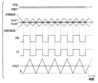
図3は、DC-DCコンバータ1の波形図である。全差動アンプ2に基準電圧VREFとフィードバック電圧VFBが入力され、差動出力信号Vout1,Vout2が出力される。差動出力信号Vout1とVout2の電位差は、基準電圧VREFとフィードバック電圧VFBの電位差に所定のゲインαを乗算した値である。
本実施形態のDC-DCコンバータ1では、全差動アンプ2を用いている。このため、基準電圧VREFとフィードバック電圧VFBの電圧差が小さくても、全差動アンプ2では、この電圧差がゲインαにより大きくすることができる。したがって、図5に示すように、HIGHの期間が短いPWM信号PMを生成することができる。言い換えれば、全差動アンプ2のゲインαにより、DC-DCコンバータのループゲインを大きくしているので、追加回路などを設けなくても、DCオフセットを小さくすることができる。
第2の実施形態は、第1の実施形態の回路に、軽負荷時動作回路を付加したDC-DCコンバータである。第2の実施形態のDC-DCコンバータ1Aは、第1の実施形態のDC-DCコンバータ1と略同じ構成を有しているので、同じ構成要素については、同じ符号を用いて説明は省略し、異なる構成要素についてのみ説明する。
Claims (4)
- 基準電圧に応じた出力電圧を生成するためのDC-DCコンバータであって、
前記基準電圧と前記出力電圧とを差動入力として、前記差動入力に応じた第1および第2の差動出力信号を出力する全差動アンプと、
前記第1および前記第2の差動出力信号に基づいて、パルス幅変調信号を生成するパルス幅変調信号生成回路と、
前記パルス幅変調信号を波形整形して、その波形整形した駆動信号を出力するドライバと、
を有し、
前記パルス幅変調信号生成回路は、
前記第1の差動出力信号と前記第2の差動出力信号を、それぞれ変調して第1の変調信号と第2の変調信号を出力する変調回路と、
前記第1の変調信号と前記第2の変調信号との比較結果に基づいて、前記パルス幅変調信号を出力するコンパレータと、
を有する、DC-DCコンバータ。 - 前記変調回路は、前記第1の差動出力信号を変調して前記第1の変調信号を出力する第1の変調器と、前記第2の差動出力信号を変調して前記第1の変調信号とは逆位相の前記第2の変調信号を出力する第2の変調器とを有する、請求項1に記載のDC-DCコンバータ。
- 前記第1の変調信号と前記第2の変調信号は、三角波信号である、請求項2に記載のDC-DCコンバータ。
- 前記パルス幅変調信号を、所定のパルス幅以上になるように設定して、前記ドライバに出力するパルス幅設定回路を有する、請求項1に記載のDC-DCコンバータ。
Priority Applications (2)
| Application Number | Priority Date | Filing Date | Title |
|---|---|---|---|
| JP2019160567A JP7170606B2 (ja) | 2019-09-03 | 2019-09-03 | Dc-dcコンバータ |
| US16/801,824 US11451146B2 (en) | 2019-09-03 | 2020-02-26 | DC-DC converter |
Applications Claiming Priority (1)
| Application Number | Priority Date | Filing Date | Title |
|---|---|---|---|
| JP2019160567A JP7170606B2 (ja) | 2019-09-03 | 2019-09-03 | Dc-dcコンバータ |
Publications (2)
| Publication Number | Publication Date |
|---|---|
| JP2021040419A JP2021040419A (ja) | 2021-03-11 |
| JP7170606B2 true JP7170606B2 (ja) | 2022-11-14 |
Family
ID=74680418
Family Applications (1)
| Application Number | Title | Priority Date | Filing Date |
|---|---|---|---|
| JP2019160567A Active JP7170606B2 (ja) | 2019-09-03 | 2019-09-03 | Dc-dcコンバータ |
Country Status (2)
| Country | Link |
|---|---|
| US (1) | US11451146B2 (ja) |
| JP (1) | JP7170606B2 (ja) |
Citations (2)
| Publication number | Priority date | Publication date | Assignee | Title |
|---|---|---|---|---|
| JP2009187430A (ja) | 2008-02-08 | 2009-08-20 | Asahi Kasei Toko Power Device Corp | レギュレータ回路 |
| JP2018108000A (ja) | 2016-12-28 | 2018-07-05 | 株式会社東芝 | 半導体装置及びdc−dcコンバータ |
Family Cites Families (18)
| Publication number | Priority date | Publication date | Assignee | Title |
|---|---|---|---|---|
| ATE420487T1 (de) | 2004-09-28 | 2009-01-15 | Nxp Bv | Strombetriebener gleichspannungswandler |
| JP4797734B2 (ja) * | 2006-03-23 | 2011-10-19 | 日本電気株式会社 | 差動増幅器とデジタル・アナログ変換器、並びに表示装置 |
| US7786712B2 (en) | 2006-12-30 | 2010-08-31 | Advanced Analogic Technologies, Inc. | High-efficiency DC/DC voltage converter including up inductive switching pre-regulator and capacitive switching post-converter |
| US7777459B2 (en) | 2006-12-30 | 2010-08-17 | Advanced Analogic Technologies, Inc. | High-efficiency DC/DC voltage converter including capacitive switching pre-converter and down inductive switching post-regulator |
| US7977927B2 (en) | 2007-08-08 | 2011-07-12 | Advanced Analogic Technologies, Inc. | Step-up DC/DC voltage converter with improved transient current capability |
| JP5040014B2 (ja) * | 2007-09-26 | 2012-10-03 | ルネサスエレクトロニクス株式会社 | 半導体集積回路装置 |
| JP5399734B2 (ja) * | 2008-09-30 | 2014-01-29 | スパンション エルエルシー | 出力電圧制御装置、出力電圧制御方法および電子機器 |
| JP2011035948A (ja) * | 2009-07-29 | 2011-02-17 | Fujitsu Semiconductor Ltd | Dc−dcコンバータ、制御回路及び電源電圧制御方法 |
| JP6145038B2 (ja) | 2013-12-26 | 2017-06-07 | 株式会社東芝 | Dc−dcコンバータ、および、半導体集積回路 |
| JP2016225951A (ja) * | 2015-06-03 | 2016-12-28 | 株式会社東芝 | 増幅回路及びアナログ/デジタル変換回路 |
| US10075073B2 (en) * | 2015-09-08 | 2018-09-11 | Rohm Co., Ltd. | DC/DC converter and switching power supply having overcurrent protection |
| JP2017055578A (ja) | 2015-09-10 | 2017-03-16 | 株式会社東芝 | Dc−dcコンバータ |
| US9561644B1 (en) | 2016-03-18 | 2017-02-07 | Xerox Corporation | System and method for compensating for malfunctioning inkjets |
| JP6794203B2 (ja) * | 2016-09-23 | 2020-12-02 | 株式会社東芝 | 半導体装置及びdc−dcコンバータ |
| JP6608866B2 (ja) | 2017-03-21 | 2019-11-20 | 株式会社東芝 | Dc−dcコンバータ |
| JP6740169B2 (ja) * | 2017-04-25 | 2020-08-12 | 株式会社東芝 | 電源装置 |
| JP6886355B2 (ja) * | 2017-06-22 | 2021-06-16 | ローム株式会社 | オペアンプ及びそれを用いたdc/dcコンバータ |
| JP7027720B2 (ja) * | 2017-08-07 | 2022-03-02 | 富士電機株式会社 | 電力変換装置 |
-
2019
- 2019-09-03 JP JP2019160567A patent/JP7170606B2/ja active Active
-
2020
- 2020-02-26 US US16/801,824 patent/US11451146B2/en active Active
Patent Citations (2)
| Publication number | Priority date | Publication date | Assignee | Title |
|---|---|---|---|---|
| JP2009187430A (ja) | 2008-02-08 | 2009-08-20 | Asahi Kasei Toko Power Device Corp | レギュレータ回路 |
| JP2018108000A (ja) | 2016-12-28 | 2018-07-05 | 株式会社東芝 | 半導体装置及びdc−dcコンバータ |
Also Published As
| Publication number | Publication date |
|---|---|
| US20210067038A1 (en) | 2021-03-04 |
| US11451146B2 (en) | 2022-09-20 |
| JP2021040419A (ja) | 2021-03-11 |
Similar Documents
| Publication | Publication Date | Title |
|---|---|---|
| JP3982342B2 (ja) | D級増幅器における三角波生成回路および該三角波生成回路を用いたd級増幅器 | |
| US9209690B2 (en) | Spread-spectrum switching regulator for eliminating modulation ripple | |
| TWI436594B (zh) | Step-up and down power supply converter and control method thereof and sawtooth wave generator and method for applying the same in the step-up and step-down power supply converter | |
| JP5627607B2 (ja) | 高圧電源及び画像形成装置 | |
| JP2005528875A (ja) | Dc−dcコンバータ | |
| JPS60215222A (ja) | 直流電源回路 | |
| CN109687853B (zh) | 脉冲宽度调制电路、对应的设备和方法 | |
| CN109217644A (zh) | 电路 | |
| CN103580480A (zh) | 直流对直流控制器与转换器 | |
| CN111585526A (zh) | 音频调制电路和电子设备 | |
| JP4785801B2 (ja) | D級増幅器 | |
| JP5009655B2 (ja) | スイッチングレギュレータ | |
| JP2002078326A (ja) | Dc−dcコンバータ用pwm制御回路 | |
| JP5340721B2 (ja) | 電源装置 | |
| US20060043952A1 (en) | Spring modulation with fast load-transient response for a voltage regulator | |
| JP7170606B2 (ja) | Dc-dcコンバータ | |
| KR101404568B1 (ko) | 전류 모드 제어의 펄스폭변조 변환 장치 | |
| US7183818B2 (en) | Triangular wave generating circuit adapted to class-D amplifier | |
| KR20050075427A (ko) | Pwm 발생기 | |
| JP2011045216A (ja) | スイッチング電源装置 | |
| JP5073580B2 (ja) | 信号増幅装置 | |
| JPWO2003021769A1 (ja) | スイッチング増幅装置 | |
| US12206332B2 (en) | Systems and methods for generating currents with variable slopes for DC-to-DC voltage converters | |
| JP2010164667A (ja) | 高圧ac電源装置、帯電装置、画像形成装置およびカラー画像形成装置 | |
| JP2005168129A (ja) | スイッチング電源回路 |
Legal Events
| Date | Code | Title | Description |
|---|---|---|---|
| A621 | Written request for application examination |
Free format text: JAPANESE INTERMEDIATE CODE: A621 Effective date: 20210922 |
|
| A977 | Report on retrieval |
Free format text: JAPANESE INTERMEDIATE CODE: A971007 Effective date: 20220729 |
|
| A131 | Notification of reasons for refusal |
Free format text: JAPANESE INTERMEDIATE CODE: A131 Effective date: 20220802 |
|
| A521 | Request for written amendment filed |
Free format text: JAPANESE INTERMEDIATE CODE: A523 Effective date: 20220922 |
|
| TRDD | Decision of grant or rejection written | ||
| A01 | Written decision to grant a patent or to grant a registration (utility model) |
Free format text: JAPANESE INTERMEDIATE CODE: A01 Effective date: 20221004 |
|
| A61 | First payment of annual fees (during grant procedure) |
Free format text: JAPANESE INTERMEDIATE CODE: A61 Effective date: 20221101 |
|
| R150 | Certificate of patent or registration of utility model |
Ref document number: 7170606 Country of ref document: JP Free format text: JAPANESE INTERMEDIATE CODE: R150 |