JP6196612B2 - 搬送装置およびセラミック部材 - Google Patents
搬送装置およびセラミック部材 Download PDFInfo
- Publication number
- JP6196612B2 JP6196612B2 JP2014503464A JP2014503464A JP6196612B2 JP 6196612 B2 JP6196612 B2 JP 6196612B2 JP 2014503464 A JP2014503464 A JP 2014503464A JP 2014503464 A JP2014503464 A JP 2014503464A JP 6196612 B2 JP6196612 B2 JP 6196612B2
- Authority
- JP
- Japan
- Prior art keywords
- ceramic
- ceramic member
- facing surface
- electrode
- axis direction
- Prior art date
- Legal status (The legal status is an assumption and is not a legal conclusion. Google has not performed a legal analysis and makes no representation as to the accuracy of the status listed.)
- Active
Links
- 239000000919 ceramic Substances 0.000 title claims description 323
- 238000001179 sorption measurement Methods 0.000 claims description 107
- 239000004020 conductor Substances 0.000 claims description 39
- 230000002093 peripheral effect Effects 0.000 claims description 5
- 239000007789 gas Substances 0.000 description 109
- 238000005485 electric heating Methods 0.000 description 34
- 238000004891 communication Methods 0.000 description 27
- 230000032258 transport Effects 0.000 description 23
- 238000000034 method Methods 0.000 description 20
- 238000005520 cutting process Methods 0.000 description 14
- 238000010586 diagram Methods 0.000 description 9
- 238000010438 heat treatment Methods 0.000 description 9
- 238000004519 manufacturing process Methods 0.000 description 9
- 239000000758 substrate Substances 0.000 description 9
- 238000010304 firing Methods 0.000 description 6
- 239000000112 cooling gas Substances 0.000 description 5
- 229910052751 metal Inorganic materials 0.000 description 5
- 239000002184 metal Substances 0.000 description 5
- 238000007650 screen-printing Methods 0.000 description 5
- CURLTUGMZLYLDI-UHFFFAOYSA-N Carbon dioxide Chemical compound O=C=O CURLTUGMZLYLDI-UHFFFAOYSA-N 0.000 description 4
- 238000005219 brazing Methods 0.000 description 4
- 229910010293 ceramic material Inorganic materials 0.000 description 4
- 238000007599 discharging Methods 0.000 description 4
- 239000011521 glass Substances 0.000 description 4
- VYPSYNLAJGMNEJ-UHFFFAOYSA-N Silicium dioxide Chemical compound O=[Si]=O VYPSYNLAJGMNEJ-UHFFFAOYSA-N 0.000 description 3
- PNEYBMLMFCGWSK-UHFFFAOYSA-N aluminium oxide Inorganic materials [O-2].[O-2].[O-2].[Al+3].[Al+3] PNEYBMLMFCGWSK-UHFFFAOYSA-N 0.000 description 3
- 229910052814 silicon oxide Inorganic materials 0.000 description 3
- XKRFYHLGVUSROY-UHFFFAOYSA-N Argon Chemical compound [Ar] XKRFYHLGVUSROY-UHFFFAOYSA-N 0.000 description 2
- 229910021417 amorphous silicon Inorganic materials 0.000 description 2
- 239000001569 carbon dioxide Substances 0.000 description 2
- 229910002092 carbon dioxide Inorganic materials 0.000 description 2
- 239000010949 copper Substances 0.000 description 2
- 230000005484 gravity Effects 0.000 description 2
- 238000010030 laminating Methods 0.000 description 2
- 239000004973 liquid crystal related substance Substances 0.000 description 2
- 239000000395 magnesium oxide Substances 0.000 description 2
- CPLXHLVBOLITMK-UHFFFAOYSA-N magnesium oxide Inorganic materials [Mg]=O CPLXHLVBOLITMK-UHFFFAOYSA-N 0.000 description 2
- AXZKOIWUVFPNLO-UHFFFAOYSA-N magnesium;oxygen(2-) Chemical compound [O-2].[Mg+2] AXZKOIWUVFPNLO-UHFFFAOYSA-N 0.000 description 2
- RVTZCBVAJQQJTK-UHFFFAOYSA-N oxygen(2-);zirconium(4+) Chemical compound [O-2].[O-2].[Zr+4] RVTZCBVAJQQJTK-UHFFFAOYSA-N 0.000 description 2
- 239000004065 semiconductor Substances 0.000 description 2
- WFKWXMTUELFFGS-UHFFFAOYSA-N tungsten Chemical compound [W] WFKWXMTUELFFGS-UHFFFAOYSA-N 0.000 description 2
- 229910052721 tungsten Inorganic materials 0.000 description 2
- 239000010937 tungsten Substances 0.000 description 2
- 229910001928 zirconium oxide Inorganic materials 0.000 description 2
- IJGRMHOSHXDMSA-UHFFFAOYSA-N Atomic nitrogen Chemical compound N#N IJGRMHOSHXDMSA-UHFFFAOYSA-N 0.000 description 1
- RYGMFSIKBFXOCR-UHFFFAOYSA-N Copper Chemical compound [Cu] RYGMFSIKBFXOCR-UHFFFAOYSA-N 0.000 description 1
- ZOKXTWBITQBERF-UHFFFAOYSA-N Molybdenum Chemical compound [Mo] ZOKXTWBITQBERF-UHFFFAOYSA-N 0.000 description 1
- XUIMIQQOPSSXEZ-UHFFFAOYSA-N Silicon Chemical compound [Si] XUIMIQQOPSSXEZ-UHFFFAOYSA-N 0.000 description 1
- BQCADISMDOOEFD-UHFFFAOYSA-N Silver Chemical compound [Ag] BQCADISMDOOEFD-UHFFFAOYSA-N 0.000 description 1
- 239000000956 alloy Substances 0.000 description 1
- 229910045601 alloy Inorganic materials 0.000 description 1
- 229910052786 argon Inorganic materials 0.000 description 1
- 239000011230 binding agent Substances 0.000 description 1
- 238000005422 blasting Methods 0.000 description 1
- 239000005388 borosilicate glass Substances 0.000 description 1
- 238000004590 computer program Methods 0.000 description 1
- 238000001816 cooling Methods 0.000 description 1
- 229910052802 copper Inorganic materials 0.000 description 1
- 238000005238 degreasing Methods 0.000 description 1
- KZHJGOXRZJKJNY-UHFFFAOYSA-N dioxosilane;oxo(oxoalumanyloxy)alumane Chemical compound O=[Si]=O.O=[Si]=O.O=[Al]O[Al]=O.O=[Al]O[Al]=O.O=[Al]O[Al]=O KZHJGOXRZJKJNY-UHFFFAOYSA-N 0.000 description 1
- 239000002241 glass-ceramic Substances 0.000 description 1
- 230000020169 heat generation Effects 0.000 description 1
- 239000001307 helium Substances 0.000 description 1
- 229910052734 helium Inorganic materials 0.000 description 1
- SWQJXJOGLNCZEY-UHFFFAOYSA-N helium atom Chemical compound [He] SWQJXJOGLNCZEY-UHFFFAOYSA-N 0.000 description 1
- 239000011261 inert gas Substances 0.000 description 1
- 238000009413 insulation Methods 0.000 description 1
- 150000002739 metals Chemical class 0.000 description 1
- 239000000203 mixture Substances 0.000 description 1
- 229910052750 molybdenum Inorganic materials 0.000 description 1
- 239000011733 molybdenum Substances 0.000 description 1
- 229910052863 mullite Inorganic materials 0.000 description 1
- TWNQGVIAIRXVLR-UHFFFAOYSA-N oxo(oxoalumanyloxy)alumane Chemical compound O=[Al]O[Al]=O TWNQGVIAIRXVLR-UHFFFAOYSA-N 0.000 description 1
- 230000000149 penetrating effect Effects 0.000 description 1
- 239000004014 plasticizer Substances 0.000 description 1
- 238000005498 polishing Methods 0.000 description 1
- 239000000843 powder Substances 0.000 description 1
- 238000007639 printing Methods 0.000 description 1
- 229910052710 silicon Inorganic materials 0.000 description 1
- 239000010703 silicon Substances 0.000 description 1
- HBMJWWWQQXIZIP-UHFFFAOYSA-N silicon carbide Chemical compound [Si+]#[C-] HBMJWWWQQXIZIP-UHFFFAOYSA-N 0.000 description 1
- 229910052709 silver Inorganic materials 0.000 description 1
- 239000004332 silver Substances 0.000 description 1
- 239000002904 solvent Substances 0.000 description 1
- 229910052715 tantalum Inorganic materials 0.000 description 1
- GUVRBAGPIYLISA-UHFFFAOYSA-N tantalum atom Chemical compound [Ta] GUVRBAGPIYLISA-UHFFFAOYSA-N 0.000 description 1
Images


Classifications
-
- H—ELECTRICITY
- H01—ELECTRIC ELEMENTS
- H01L—SEMICONDUCTOR DEVICES NOT COVERED BY CLASS H10
- H01L21/00—Processes or apparatus adapted for the manufacture or treatment of semiconductor or solid state devices or of parts thereof
- H01L21/67—Apparatus specially adapted for handling semiconductor or electric solid state devices during manufacture or treatment thereof; Apparatus specially adapted for handling wafers during manufacture or treatment of semiconductor or electric solid state devices or components ; Apparatus not specifically provided for elsewhere
- H01L21/677—Apparatus specially adapted for handling semiconductor or electric solid state devices during manufacture or treatment thereof; Apparatus specially adapted for handling wafers during manufacture or treatment of semiconductor or electric solid state devices or components ; Apparatus not specifically provided for elsewhere for conveying, e.g. between different workstations
- H01L21/67703—Apparatus specially adapted for handling semiconductor or electric solid state devices during manufacture or treatment thereof; Apparatus specially adapted for handling wafers during manufacture or treatment of semiconductor or electric solid state devices or components ; Apparatus not specifically provided for elsewhere for conveying, e.g. between different workstations between different workstations
- H01L21/67712—Apparatus specially adapted for handling semiconductor or electric solid state devices during manufacture or treatment thereof; Apparatus specially adapted for handling wafers during manufacture or treatment of semiconductor or electric solid state devices or components ; Apparatus not specifically provided for elsewhere for conveying, e.g. between different workstations between different workstations the substrate being handled substantially vertically
-
- H—ELECTRICITY
- H02—GENERATION; CONVERSION OR DISTRIBUTION OF ELECTRIC POWER
- H02N—ELECTRIC MACHINES NOT OTHERWISE PROVIDED FOR
- H02N13/00—Clutches or holding devices using electrostatic attraction, e.g. using Johnson-Rahbek effect
-
- B—PERFORMING OPERATIONS; TRANSPORTING
- B25—HAND TOOLS; PORTABLE POWER-DRIVEN TOOLS; MANIPULATORS
- B25J—MANIPULATORS; CHAMBERS PROVIDED WITH MANIPULATION DEVICES
- B25J11/00—Manipulators not otherwise provided for
- B25J11/0095—Manipulators transporting wafers
-
- B—PERFORMING OPERATIONS; TRANSPORTING
- B25—HAND TOOLS; PORTABLE POWER-DRIVEN TOOLS; MANIPULATORS
- B25J—MANIPULATORS; CHAMBERS PROVIDED WITH MANIPULATION DEVICES
- B25J15/00—Gripping heads and other end effectors
- B25J15/0014—Gripping heads and other end effectors having fork, comb or plate shaped means for engaging the lower surface on a object to be transported
-
- B—PERFORMING OPERATIONS; TRANSPORTING
- B25—HAND TOOLS; PORTABLE POWER-DRIVEN TOOLS; MANIPULATORS
- B25J—MANIPULATORS; CHAMBERS PROVIDED WITH MANIPULATION DEVICES
- B25J15/00—Gripping heads and other end effectors
- B25J15/0085—Gripping heads and other end effectors with means for applying an electrostatic force on the object to be gripped
-
- B—PERFORMING OPERATIONS; TRANSPORTING
- B25—HAND TOOLS; PORTABLE POWER-DRIVEN TOOLS; MANIPULATORS
- B25J—MANIPULATORS; CHAMBERS PROVIDED WITH MANIPULATION DEVICES
- B25J15/00—Gripping heads and other end effectors
- B25J15/06—Gripping heads and other end effectors with vacuum or magnetic holding means
- B25J15/0616—Gripping heads and other end effectors with vacuum or magnetic holding means with vacuum
-
- H—ELECTRICITY
- H01—ELECTRIC ELEMENTS
- H01L—SEMICONDUCTOR DEVICES NOT COVERED BY CLASS H10
- H01L21/00—Processes or apparatus adapted for the manufacture or treatment of semiconductor or solid state devices or of parts thereof
- H01L21/67—Apparatus specially adapted for handling semiconductor or electric solid state devices during manufacture or treatment thereof; Apparatus specially adapted for handling wafers during manufacture or treatment of semiconductor or electric solid state devices or components ; Apparatus not specifically provided for elsewhere
- H01L21/67005—Apparatus not specifically provided for elsewhere
- H01L21/67011—Apparatus for manufacture or treatment
- H01L21/67098—Apparatus for thermal treatment
- H01L21/67103—Apparatus for thermal treatment mainly by conduction
-
- H—ELECTRICITY
- H01—ELECTRIC ELEMENTS
- H01L—SEMICONDUCTOR DEVICES NOT COVERED BY CLASS H10
- H01L21/00—Processes or apparatus adapted for the manufacture or treatment of semiconductor or solid state devices or of parts thereof
- H01L21/67—Apparatus specially adapted for handling semiconductor or electric solid state devices during manufacture or treatment thereof; Apparatus specially adapted for handling wafers during manufacture or treatment of semiconductor or electric solid state devices or components ; Apparatus not specifically provided for elsewhere
- H01L21/677—Apparatus specially adapted for handling semiconductor or electric solid state devices during manufacture or treatment thereof; Apparatus specially adapted for handling wafers during manufacture or treatment of semiconductor or electric solid state devices or components ; Apparatus not specifically provided for elsewhere for conveying, e.g. between different workstations
- H01L21/67739—Apparatus specially adapted for handling semiconductor or electric solid state devices during manufacture or treatment thereof; Apparatus specially adapted for handling wafers during manufacture or treatment of semiconductor or electric solid state devices or components ; Apparatus not specifically provided for elsewhere for conveying, e.g. between different workstations into and out of processing chamber
- H01L21/67742—Mechanical parts of transfer devices
-
- H—ELECTRICITY
- H01—ELECTRIC ELEMENTS
- H01L—SEMICONDUCTOR DEVICES NOT COVERED BY CLASS H10
- H01L21/00—Processes or apparatus adapted for the manufacture or treatment of semiconductor or solid state devices or of parts thereof
- H01L21/67—Apparatus specially adapted for handling semiconductor or electric solid state devices during manufacture or treatment thereof; Apparatus specially adapted for handling wafers during manufacture or treatment of semiconductor or electric solid state devices or components ; Apparatus not specifically provided for elsewhere
- H01L21/683—Apparatus specially adapted for handling semiconductor or electric solid state devices during manufacture or treatment thereof; Apparatus specially adapted for handling wafers during manufacture or treatment of semiconductor or electric solid state devices or components ; Apparatus not specifically provided for elsewhere for supporting or gripping
- H01L21/6831—Apparatus specially adapted for handling semiconductor or electric solid state devices during manufacture or treatment thereof; Apparatus specially adapted for handling wafers during manufacture or treatment of semiconductor or electric solid state devices or components ; Apparatus not specifically provided for elsewhere for supporting or gripping using electrostatic chucks
- H01L21/6833—Details of electrostatic chucks
Landscapes
- Engineering & Computer Science (AREA)
- Robotics (AREA)
- Physics & Mathematics (AREA)
- Condensed Matter Physics & Semiconductors (AREA)
- General Physics & Mathematics (AREA)
- Manufacturing & Machinery (AREA)
- Computer Hardware Design (AREA)
- Microelectronics & Electronic Packaging (AREA)
- Power Engineering (AREA)
- Mechanical Engineering (AREA)
- Container, Conveyance, Adherence, Positioning, Of Wafer (AREA)
- Manipulator (AREA)
Description
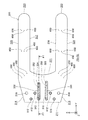
図1は、搬送装置10の構成を示す説明図である。搬送装置10は、被搬送体90を搬送する。本実施形態では、搬送装置10は、半導体製造装置の一部を構成する装置であり、被搬送体90は、円板状の誘電体であるシリコン製のウェハである。
第2実施形態の説明では、第1実施形態と同様の構成については第1実施形態と同じ符号を用い、形状や配置などが異なるものの第1実施形態に対応する構成については第1実施形態の符号に英文字「A」を付した符号を用いる。
第3実施形態の説明では、第1実施形態と同様の構成については第1実施形態と同じ符号を用い、形状や配置などが異なるものの第1実施形態に対応する構成については第1実施形態の符号に英文字「B」を付した符号を用いる。
第4実施形態の説明では、第1実施形態と同様の構成については第1実施形態と同じ符号を用い、形状や配置などが異なるものの第1実施形態に対応する構成については第1実施形態の符号に英文字「C」を付した符号を用いる。
第5実施形態の説明では、第1実施形態と同様の構成については第1実施形態と同じ符号を用い、形状や配置などが異なるものの第1実施形態に対応する構成については第1実施形態の符号に英文字「D」を付した符号を用いる。
第6実施形態の説明では、第1実施形態と同様の構成については第1実施形態と同じ符号を用い、形状や配置などが異なるものの第1実施形態に対応する構成については第1実施形態の符号に英文字「E」を付した符号を用いる。
第7実施形態の説明では、第1実施形態と同様の構成については第1実施形態と同じ符号を用い、形状や配置などが異なるものの第1実施形態に対応する構成については第1実施形態の符号に英文字「F」を付した符号を用いる。
第8実施形態の説明では、第1実施形態と同様の構成については第1実施形態と同じ符号を用い、形状や配置などが異なるものの第1実施形態に対応する構成については第1実施形態の符号に英文字「G」を付した符号を用いる。
第9実施形態の説明では、第1実施形態と同様の構成については第1実施形態と同じ符号を用い、形状や配置などが異なるものの第1実施形態に対応する構成については第1実施形態の符号に英文字「H」を付した符号を用いる。
第10実施形態の説明では、第1実施形態と同様の構成については第1実施形態と同じ符号を用い、形状や配置などが異なるものの第1実施形態に対応する構成については第1実施形態の符号に英文字「I」を付した符号を用いる。
第11実施形態の説明では、第1実施形態と同様の構成については第1実施形態と同じ符号を用い、形状や配置などが異なるものの第1実施形態に対応する構成については第1実施形態の符号に英文字「J」を付した符号を用いる。
以上、本発明の実施形態について説明したが、本発明はこうした実施形態に何ら限定されるものではなく、本発明の趣旨を逸脱しない範囲内において様々な形態で実施し得ることは勿論である。
90…被搬送体
100…制御部
200,200A〜200J…セラミック部材
211…基端面
213…基端側面
214…基端側面
215…基端上面
216…底面
218…貫通孔
219,219A…基端段差面
221…内側面
222…先端面
223…先端面
224,224C…外側面
225,225C…外側面
226,226C…内側面
227,227C…内側面
231,231D,231E,231H,231I,231J…対向面
232,232F,232H,232I,232J…対向面
233…対向面
234…対向面
235,235E,235F…対向面
242…先端上面
243…先端上面
248,248B…先端段差面
249,249B…先端段差面
291〜297…セラミック層
312,312F…給電口
316,316F…給電口
332,336…ランド
352,354,356,358…ビア
372,372F,372H,372I,372J…吸着電極
374…吸着電極
376,376F,376H,376I,376J…吸着電極
378…吸着電極
412,412F…負圧供給口
430,430F,430G…負圧連通路
450,450F…吸着孔
512…給電口
516…給電口
532,536…ランド
552,553,554,556,557,558…ビア
572,572G…電熱体
574…電熱体
576…電熱体
612…ガス供給口
630,630A,630B,630C…ガス連通路
650,650A,650B,650C…ガス放出孔
710…アーム機構
720…移動機構
830…吸着電極駆動部
840…負圧供給部
850…電熱体駆動部
860…処理ガス供給部
Claims (4)
- 搬送装置において被搬送体を保持した状態で前記被搬送体と共に移動可能に構成されたセラミック部材であって、
絶縁性を有し、一体焼成された複数のセラミック層と、
前記複数のセラミック層の内部であって前記複数のセラミック層のうちの第1のセラミック層上に形成され、静電力によって誘電体を吸着可能に構成された電極である吸着電極と、
前記セラミック部材の外部から前記吸着電極に対する電力の供給を受け付ける給電口と、
前記複数のセラミック層のうち前記第1のセラミック層とは異なる第2のセラミック層上に形成され、前記給電口を通じて受電可能に構成された導体であるランドと、
前記複数のセラミック層の少なくとも1つを貫通して前記吸着電極と前記ランドとの間を電気的に接続する導体であるビアと、
前記複数のセラミック層の層面方向に沿った面であって前記被搬送体を保持した状態で前記被搬送体に対向する面である対向面と、
前記対向面の外周側に形成された面であって前記対向面と同じ方向を向く基端上面と、
を備え、
前記ランドが、前記対向面の直下と前記基端上面の直下とに跨って形成され、
前記複数のセラミック層の層面方向に沿った面であって前記被搬送体を保持した状態で前記被搬送体に対向する前記対向面である第1の対向面および第2の対向面と、
前記第1の対向面に形成され、前記第1の対向面に負圧を提供することによって前記被搬送体を吸着可能に構成された孔である吸着孔と、をさらに備え、
前記層面方向に直交する厚さ方向から見て、前記吸着電極の少なくとも一部は、前記第2の対向面に重なり、
前記第2の対向面は、前記第1の対向面よりも前記被搬送体側に位置し、前記厚さ方向から見て前記吸着孔および前記第1の対向面を取り囲む、セラミック部材。 - 請求項1に記載のセラミック部材であって、
前記吸着電極は、前記ランドよりも前記被搬送体を保持する側に位置する、セラミック部材。 - 請求項1または2に記載のセラミック部材であって、
前記吸着電極は、相互に異なる極性の電位になるように構成された第1電極および第2電極を含み、
前記第1電極および前記第2電極の各々は、前記厚さ方向から見て前記第2の対向面に対して略均等に重なる、セラミック部材。 - 請求項1から請求項3までのいずれか一項に記載のセラミック部材を用いて前記被搬送体を搬送する搬送装置。
Applications Claiming Priority (3)
| Application Number | Priority Date | Filing Date | Title |
|---|---|---|---|
| JP2012050209 | 2012-03-07 | ||
| JP2012050209 | 2012-03-07 | ||
| PCT/JP2013/001244 WO2013132803A1 (ja) | 2012-03-07 | 2013-02-28 | 搬送装置およびセラミック部材 |
Related Child Applications (1)
| Application Number | Title | Priority Date | Filing Date |
|---|---|---|---|
| JP2017153083A Division JP6359736B2 (ja) | 2012-03-07 | 2017-08-08 | 搬送装置およびセラミック部材 |
Publications (2)
| Publication Number | Publication Date |
|---|---|
| JPWO2013132803A1 JPWO2013132803A1 (ja) | 2015-07-30 |
| JP6196612B2 true JP6196612B2 (ja) | 2017-09-13 |
Family
ID=49116299
Family Applications (2)
| Application Number | Title | Priority Date | Filing Date |
|---|---|---|---|
| JP2014503464A Active JP6196612B2 (ja) | 2012-03-07 | 2013-02-28 | 搬送装置およびセラミック部材 |
| JP2017153083A Active JP6359736B2 (ja) | 2012-03-07 | 2017-08-08 | 搬送装置およびセラミック部材 |
Family Applications After (1)
| Application Number | Title | Priority Date | Filing Date |
|---|---|---|---|
| JP2017153083A Active JP6359736B2 (ja) | 2012-03-07 | 2017-08-08 | 搬送装置およびセラミック部材 |
Country Status (5)
| Country | Link |
|---|---|
| US (1) | US9276504B2 (ja) |
| JP (2) | JP6196612B2 (ja) |
| KR (1) | KR101800072B1 (ja) |
| TW (1) | TWI538790B (ja) |
| WO (1) | WO2013132803A1 (ja) |
Families Citing this family (2)
| Publication number | Priority date | Publication date | Assignee | Title |
|---|---|---|---|---|
| JP7036905B2 (ja) * | 2018-04-26 | 2022-03-15 | 京セラ株式会社 | フォーカスリング搬送部材およびこれを備えるプラズマ処理装置 |
| CN114906605B (zh) * | 2022-04-25 | 2024-07-09 | 重庆安都陶瓷有限公司 | 一种用于抓取半成品陶罐的机械手 |
Family Cites Families (20)
| Publication number | Priority date | Publication date | Assignee | Title |
|---|---|---|---|---|
| JP3193034B2 (ja) | 1990-05-31 | 2001-07-30 | 京セラ株式会社 | 真空ピンセット |
| JPH0463644U (ja) * | 1990-10-11 | 1992-05-29 | ||
| US5191506A (en) * | 1991-05-02 | 1993-03-02 | International Business Machines Corporation | Ceramic electrostatic chuck |
| JPH09213455A (ja) | 1996-02-05 | 1997-08-15 | Kyocera Corp | ウエハ保持装置の給電構造 |
| JPH09223729A (ja) * | 1996-02-19 | 1997-08-26 | Kyocera Corp | 静電チャック |
| JPH10242256A (ja) * | 1997-02-26 | 1998-09-11 | Kyocera Corp | 静電チャック |
| US6255601B1 (en) * | 1997-04-01 | 2001-07-03 | Applied Materials, Inc. | Conductive feedthrough for a ceramic body and method of fabricating same |
| US6303879B1 (en) | 1997-04-01 | 2001-10-16 | Applied Materials, Inc. | Laminated ceramic with multilayer electrodes and method of fabrication |
| US5909355A (en) * | 1997-12-02 | 1999-06-01 | Applied Materials, Inc. | Ceramic electrostatic chuck and method of fabricating same |
| JP3805134B2 (ja) * | 1999-05-25 | 2006-08-02 | 東陶機器株式会社 | 絶縁性基板吸着用静電チャック |
| JP2001267400A (ja) * | 2000-03-16 | 2001-09-28 | Kyocera Corp | ウエハ支持部材 |
| US6483690B1 (en) * | 2001-06-28 | 2002-11-19 | Lam Research Corporation | Ceramic electrostatic chuck assembly and method of making |
| JP2005197391A (ja) | 2004-01-06 | 2005-07-21 | Ibiden Co Ltd | プラズマ発生装置用電極埋設部材 |
| JP2007222967A (ja) * | 2006-02-21 | 2007-09-06 | Shinko Electric Ind Co Ltd | 薄物ワーク搬送用のピンセット |
| JP4298739B2 (ja) * | 2006-11-06 | 2009-07-22 | キヤノン株式会社 | 基板吸着装置 |
| KR101119075B1 (ko) * | 2007-03-12 | 2012-03-15 | 주식회사 코미코 | 웨이퍼 이송 장치 |
| JP5202028B2 (ja) | 2008-02-26 | 2013-06-05 | 京セラ株式会社 | 真空ピンセットおよびこれを用いた基板搬送装置ならびに基板処理装置 |
| JP2011049425A (ja) * | 2009-08-28 | 2011-03-10 | Ngk Spark Plug Co Ltd | 半導体製造装置用部品 |
| JP2011077288A (ja) * | 2009-09-30 | 2011-04-14 | Tokyo Electron Ltd | 搬送装置 |
| JPWO2011077678A1 (ja) * | 2009-12-22 | 2013-05-02 | 株式会社アルバック | 基板保持装置 |
-
2013
- 2013-02-28 WO PCT/JP2013/001244 patent/WO2013132803A1/ja active Application Filing
- 2013-02-28 JP JP2014503464A patent/JP6196612B2/ja active Active
- 2013-02-28 US US14/383,301 patent/US9276504B2/en not_active Expired - Fee Related
- 2013-02-28 KR KR1020147024822A patent/KR101800072B1/ko active IP Right Grant
- 2013-03-06 TW TW102107764A patent/TWI538790B/zh active
-
2017
- 2017-08-08 JP JP2017153083A patent/JP6359736B2/ja active Active
Also Published As
| Publication number | Publication date |
|---|---|
| JP6359736B2 (ja) | 2018-07-25 |
| JP2017208572A (ja) | 2017-11-24 |
| US9276504B2 (en) | 2016-03-01 |
| KR101800072B1 (ko) | 2017-11-21 |
| JPWO2013132803A1 (ja) | 2015-07-30 |
| WO2013132803A1 (ja) | 2013-09-12 |
| TW201347932A (zh) | 2013-12-01 |
| US20150021944A1 (en) | 2015-01-22 |
| TWI538790B (zh) | 2016-06-21 |
| KR20140131946A (ko) | 2014-11-14 |
Similar Documents
| Publication | Publication Date | Title |
|---|---|---|
| JP6463938B2 (ja) | 静電チャック | |
| KR102257409B1 (ko) | 유지 장치 | |
| KR20170045105A (ko) | 가열부재, 정전 척 및 세라믹 히터 | |
| KR102659507B1 (ko) | 세라믹 기판 및 정전 척 | |
| JP6359736B2 (ja) | 搬送装置およびセラミック部材 | |
| JP6831269B2 (ja) | セラミックヒータ | |
| JP7449768B2 (ja) | セラミックス基板及びその製造方法、静電チャック、基板固定装置、半導体装置用パッケージ | |
| JP5963242B2 (ja) | 搬送装置およびセラミック部材 | |
| JP6106659B2 (ja) | 搬送装置およびセラミック部材 | |
| JP5214414B2 (ja) | 半導体製造装置用接続部及び半導体製造装置用接続部の形成方法 | |
| JP2018006559A (ja) | 静電チャック、および、静電チャックの製造方法 | |
| JP6068118B2 (ja) | 搬送装置及び搬送用部材 | |
| WO2019208439A1 (ja) | フォーカスリング搬送部材およびこれを備えるプラズマ処理装置 | |
| JP2001077185A (ja) | 静電チャック及びその製造方法 | |
| KR20230030050A (ko) | 유지 장치 | |
| JP2008172255A (ja) | 静電チャック | |
| JP5642722B2 (ja) | 半導体製造装置用接続部及び半導体製造装置用接続部の形成方法 | |
| JP7280707B2 (ja) | 保持装置および保持装置の製造方法 | |
| JPH04304942A (ja) | 静電チャック基板および静電チャック | |
| KR20230138930A (ko) | 세라믹 기판, 세라믹 기판의 제조 방법, 정전 척, 기판 고정 장치, 및 반도체 장치용 패키지 | |
| JP2024138913A (ja) | 静電チャック | |
| JP6334338B2 (ja) | 試料保持具 |
Legal Events
| Date | Code | Title | Description |
|---|---|---|---|
| A521 | Request for written amendment filed |
Free format text: JAPANESE INTERMEDIATE CODE: A523 Effective date: 20160113 |
|
| A621 | Written request for application examination |
Free format text: JAPANESE INTERMEDIATE CODE: A621 Effective date: 20160113 |
|
| A131 | Notification of reasons for refusal |
Free format text: JAPANESE INTERMEDIATE CODE: A131 Effective date: 20160906 |
|
| RD04 | Notification of resignation of power of attorney |
Free format text: JAPANESE INTERMEDIATE CODE: A7424 Effective date: 20161006 |
|
| RD02 | Notification of acceptance of power of attorney |
Free format text: JAPANESE INTERMEDIATE CODE: A7422 Effective date: 20161024 |
|
| A521 | Request for written amendment filed |
Free format text: JAPANESE INTERMEDIATE CODE: A523 Effective date: 20161028 |
|
| A131 | Notification of reasons for refusal |
Free format text: JAPANESE INTERMEDIATE CODE: A131 Effective date: 20170222 |
|
| A521 | Request for written amendment filed |
Free format text: JAPANESE INTERMEDIATE CODE: A523 Effective date: 20170317 |
|
| TRDD | Decision of grant or rejection written | ||
| A01 | Written decision to grant a patent or to grant a registration (utility model) |
Free format text: JAPANESE INTERMEDIATE CODE: A01 Effective date: 20170728 |
|
| A61 | First payment of annual fees (during grant procedure) |
Free format text: JAPANESE INTERMEDIATE CODE: A61 Effective date: 20170818 |
|
| R150 | Certificate of patent or registration of utility model |
Ref document number: 6196612 Country of ref document: JP Free format text: JAPANESE INTERMEDIATE CODE: R150 |
|
| RD03 | Notification of appointment of power of attorney |
Free format text: JAPANESE INTERMEDIATE CODE: R3D03 |
|
| RD04 | Notification of resignation of power of attorney |
Free format text: JAPANESE INTERMEDIATE CODE: R3D04 |
|
| R250 | Receipt of annual fees |
Free format text: JAPANESE INTERMEDIATE CODE: R250 |
|
| R250 | Receipt of annual fees |
Free format text: JAPANESE INTERMEDIATE CODE: R250 |
|
| R250 | Receipt of annual fees |
Free format text: JAPANESE INTERMEDIATE CODE: R250 |
|
| S531 | Written request for registration of change of domicile |
Free format text: JAPANESE INTERMEDIATE CODE: R313531 |
|
| R350 | Written notification of registration of transfer |
Free format text: JAPANESE INTERMEDIATE CODE: R350 |
|
| R250 | Receipt of annual fees |
Free format text: JAPANESE INTERMEDIATE CODE: R250 |
|
| R250 | Receipt of annual fees |
Free format text: JAPANESE INTERMEDIATE CODE: R250 |