JP5659182B2 - Nitride semiconductor device - Google Patents
Nitride semiconductor device Download PDFInfo
- Publication number
- JP5659182B2 JP5659182B2 JP2012068143A JP2012068143A JP5659182B2 JP 5659182 B2 JP5659182 B2 JP 5659182B2 JP 2012068143 A JP2012068143 A JP 2012068143A JP 2012068143 A JP2012068143 A JP 2012068143A JP 5659182 B2 JP5659182 B2 JP 5659182B2
- Authority
- JP
- Japan
- Prior art keywords
- electrode
- nitride semiconductor
- semiconductor layer
- layer
- anode
- Prior art date
- Legal status (The legal status is an assumption and is not a legal conclusion. Google has not performed a legal analysis and makes no representation as to the accuracy of the status listed.)
- Active
Links
- 239000004065 semiconductor Substances 0.000 title claims description 161
- 150000004767 nitrides Chemical class 0.000 title claims description 157
- 239000000758 substrate Substances 0.000 claims description 26
- 238000002955 isolation Methods 0.000 claims description 20
- 230000005669 field effect Effects 0.000 claims description 14
- 230000004888 barrier function Effects 0.000 claims description 11
- 230000005533 two-dimensional electron gas Effects 0.000 claims description 5
- 230000004048 modification Effects 0.000 description 25
- 238000012986 modification Methods 0.000 description 25
- 229910002601 GaN Inorganic materials 0.000 description 9
- 239000003990 capacitor Substances 0.000 description 9
- 239000000463 material Substances 0.000 description 9
- JMASRVWKEDWRBT-UHFFFAOYSA-N Gallium nitride Chemical compound [Ga]#N JMASRVWKEDWRBT-UHFFFAOYSA-N 0.000 description 8
- 230000003071 parasitic effect Effects 0.000 description 8
- 238000010586 diagram Methods 0.000 description 4
- 230000015556 catabolic process Effects 0.000 description 3
- 238000006243 chemical reaction Methods 0.000 description 3
- 230000007257 malfunction Effects 0.000 description 3
- 239000010949 copper Substances 0.000 description 2
- 230000006378 damage Effects 0.000 description 2
- 238000000034 method Methods 0.000 description 2
- 230000010287 polarization Effects 0.000 description 2
- HBMJWWWQQXIZIP-UHFFFAOYSA-N silicon carbide Chemical compound [Si+]#[C-] HBMJWWWQQXIZIP-UHFFFAOYSA-N 0.000 description 2
- RYGMFSIKBFXOCR-UHFFFAOYSA-N Copper Chemical compound [Cu] RYGMFSIKBFXOCR-UHFFFAOYSA-N 0.000 description 1
- RNQKDQAVIXDKAG-UHFFFAOYSA-N aluminum gallium Chemical compound [Al].[Ga] RNQKDQAVIXDKAG-UHFFFAOYSA-N 0.000 description 1
- 230000015572 biosynthetic process Effects 0.000 description 1
- 229910052802 copper Inorganic materials 0.000 description 1
- 230000000694 effects Effects 0.000 description 1
- 238000005530 etching Methods 0.000 description 1
- 238000009499 grossing Methods 0.000 description 1
- 125000005842 heteroatom Chemical group 0.000 description 1
- 238000005468 ion implantation Methods 0.000 description 1
- 238000010030 laminating Methods 0.000 description 1
- 229910052751 metal Inorganic materials 0.000 description 1
- 239000002184 metal Substances 0.000 description 1
- 229910052710 silicon Inorganic materials 0.000 description 1
- 239000010703 silicon Substances 0.000 description 1
- 229910010271 silicon carbide Inorganic materials 0.000 description 1
- 229910000679 solder Inorganic materials 0.000 description 1
Images


Classifications
-
- H—ELECTRICITY
- H10—SEMICONDUCTOR DEVICES; ELECTRIC SOLID-STATE DEVICES NOT OTHERWISE PROVIDED FOR
- H10D—INORGANIC ELECTRIC SEMICONDUCTOR DEVICES
- H10D84/00—Integrated devices formed in or on semiconductor substrates that comprise only semiconducting layers, e.g. on Si wafers or on GaAs-on-Si wafers
- H10D84/01—Manufacture or treatment
- H10D84/02—Manufacture or treatment characterised by using material-based technologies
- H10D84/05—Manufacture or treatment characterised by using material-based technologies using Group III-V technology
-
- H—ELECTRICITY
- H02—GENERATION; CONVERSION OR DISTRIBUTION OF ELECTRIC POWER
- H02M—APPARATUS FOR CONVERSION BETWEEN AC AND AC, BETWEEN AC AND DC, OR BETWEEN DC AND DC, AND FOR USE WITH MAINS OR SIMILAR POWER SUPPLY SYSTEMS; CONVERSION OF DC OR AC INPUT POWER INTO SURGE OUTPUT POWER; CONTROL OR REGULATION THEREOF
- H02M3/00—Conversion of DC power input into DC power output
- H02M3/02—Conversion of DC power input into DC power output without intermediate conversion into AC
- H02M3/04—Conversion of DC power input into DC power output without intermediate conversion into AC by static converters
- H02M3/10—Conversion of DC power input into DC power output without intermediate conversion into AC by static converters using discharge tubes with control electrode or semiconductor devices with control electrode
- H02M3/145—Conversion of DC power input into DC power output without intermediate conversion into AC by static converters using discharge tubes with control electrode or semiconductor devices with control electrode using devices of a triode or transistor type requiring continuous application of a control signal
- H02M3/155—Conversion of DC power input into DC power output without intermediate conversion into AC by static converters using discharge tubes with control electrode or semiconductor devices with control electrode using devices of a triode or transistor type requiring continuous application of a control signal using semiconductor devices only
- H02M3/156—Conversion of DC power input into DC power output without intermediate conversion into AC by static converters using discharge tubes with control electrode or semiconductor devices with control electrode using devices of a triode or transistor type requiring continuous application of a control signal using semiconductor devices only with automatic control of output voltage or current, e.g. switching regulators
-
- H—ELECTRICITY
- H10—SEMICONDUCTOR DEVICES; ELECTRIC SOLID-STATE DEVICES NOT OTHERWISE PROVIDED FOR
- H10D—INORGANIC ELECTRIC SEMICONDUCTOR DEVICES
- H10D30/00—Field-effect transistors [FET]
- H10D30/40—FETs having zero-dimensional [0D], one-dimensional [1D] or two-dimensional [2D] charge carrier gas channels
- H10D30/47—FETs having zero-dimensional [0D], one-dimensional [1D] or two-dimensional [2D] charge carrier gas channels having 2D charge carrier gas channels, e.g. nanoribbon FETs or high electron mobility transistors [HEMT]
- H10D30/471—High electron mobility transistors [HEMT] or high hole mobility transistors [HHMT]
- H10D30/475—High electron mobility transistors [HEMT] or high hole mobility transistors [HHMT] having wider bandgap layer formed on top of lower bandgap active layer, e.g. undoped barrier HEMTs such as i-AlGaN/GaN HEMTs
-
- H—ELECTRICITY
- H10—SEMICONDUCTOR DEVICES; ELECTRIC SOLID-STATE DEVICES NOT OTHERWISE PROVIDED FOR
- H10D—INORGANIC ELECTRIC SEMICONDUCTOR DEVICES
- H10D8/00—Diodes
- H10D8/60—Schottky-barrier diodes
-
- H—ELECTRICITY
- H10—SEMICONDUCTOR DEVICES; ELECTRIC SOLID-STATE DEVICES NOT OTHERWISE PROVIDED FOR
- H10D—INORGANIC ELECTRIC SEMICONDUCTOR DEVICES
- H10D84/00—Integrated devices formed in or on semiconductor substrates that comprise only semiconducting layers, e.g. on Si wafers or on GaAs-on-Si wafers
- H10D84/01—Manufacture or treatment
-
- H—ELECTRICITY
- H10—SEMICONDUCTOR DEVICES; ELECTRIC SOLID-STATE DEVICES NOT OTHERWISE PROVIDED FOR
- H10D—INORGANIC ELECTRIC SEMICONDUCTOR DEVICES
- H10D84/00—Integrated devices formed in or on semiconductor substrates that comprise only semiconducting layers, e.g. on Si wafers or on GaAs-on-Si wafers
- H10D84/80—Integrated devices formed in or on semiconductor substrates that comprise only semiconducting layers, e.g. on Si wafers or on GaAs-on-Si wafers characterised by the integration of at least one component covered by groups H10D12/00 or H10D30/00, e.g. integration of IGFETs
- H10D84/811—Combinations of field-effect devices and one or more diodes, capacitors or resistors
-
- H—ELECTRICITY
- H10—SEMICONDUCTOR DEVICES; ELECTRIC SOLID-STATE DEVICES NOT OTHERWISE PROVIDED FOR
- H10D—INORGANIC ELECTRIC SEMICONDUCTOR DEVICES
- H10D89/00—Aspects of integrated devices not covered by groups H10D84/00 - H10D88/00
- H10D89/10—Integrated device layouts
-
- H—ELECTRICITY
- H01—ELECTRIC ELEMENTS
- H01L—SEMICONDUCTOR DEVICES NOT COVERED BY CLASS H10
- H01L2924/00—Indexing scheme for arrangements or methods for connecting or disconnecting semiconductor or solid-state bodies as covered by H01L24/00
- H01L2924/0001—Technical content checked by a classifier
- H01L2924/0002—Not covered by any one of groups H01L24/00, H01L24/00 and H01L2224/00
-
- H—ELECTRICITY
- H02—GENERATION; CONVERSION OR DISTRIBUTION OF ELECTRIC POWER
- H02M—APPARATUS FOR CONVERSION BETWEEN AC AND AC, BETWEEN AC AND DC, OR BETWEEN DC AND DC, AND FOR USE WITH MAINS OR SIMILAR POWER SUPPLY SYSTEMS; CONVERSION OF DC OR AC INPUT POWER INTO SURGE OUTPUT POWER; CONTROL OR REGULATION THEREOF
- H02M1/00—Details of apparatus for conversion
- H02M1/0067—Converter structures employing plural converter units, other than for parallel operation of the units on a single load
- H02M1/007—Plural converter units in cascade
-
- H—ELECTRICITY
- H02—GENERATION; CONVERSION OR DISTRIBUTION OF ELECTRIC POWER
- H02M—APPARATUS FOR CONVERSION BETWEEN AC AND AC, BETWEEN AC AND DC, OR BETWEEN DC AND DC, AND FOR USE WITH MAINS OR SIMILAR POWER SUPPLY SYSTEMS; CONVERSION OF DC OR AC INPUT POWER INTO SURGE OUTPUT POWER; CONTROL OR REGULATION THEREOF
- H02M3/00—Conversion of DC power input into DC power output
- H02M3/02—Conversion of DC power input into DC power output without intermediate conversion into AC
- H02M3/04—Conversion of DC power input into DC power output without intermediate conversion into AC by static converters
- H02M3/10—Conversion of DC power input into DC power output without intermediate conversion into AC by static converters using discharge tubes with control electrode or semiconductor devices with control electrode
- H02M3/145—Conversion of DC power input into DC power output without intermediate conversion into AC by static converters using discharge tubes with control electrode or semiconductor devices with control electrode using devices of a triode or transistor type requiring continuous application of a control signal
- H02M3/155—Conversion of DC power input into DC power output without intermediate conversion into AC by static converters using discharge tubes with control electrode or semiconductor devices with control electrode using devices of a triode or transistor type requiring continuous application of a control signal using semiconductor devices only
-
- H—ELECTRICITY
- H02—GENERATION; CONVERSION OR DISTRIBUTION OF ELECTRIC POWER
- H02M—APPARATUS FOR CONVERSION BETWEEN AC AND AC, BETWEEN AC AND DC, OR BETWEEN DC AND DC, AND FOR USE WITH MAINS OR SIMILAR POWER SUPPLY SYSTEMS; CONVERSION OF DC OR AC INPUT POWER INTO SURGE OUTPUT POWER; CONTROL OR REGULATION THEREOF
- H02M3/00—Conversion of DC power input into DC power output
- H02M3/22—Conversion of DC power input into DC power output with intermediate conversion into AC
- H02M3/24—Conversion of DC power input into DC power output with intermediate conversion into AC by static converters
- H02M3/28—Conversion of DC power input into DC power output with intermediate conversion into AC by static converters using discharge tubes with control electrode or semiconductor devices with control electrode to produce the intermediate AC
- H02M3/325—Conversion of DC power input into DC power output with intermediate conversion into AC by static converters using discharge tubes with control electrode or semiconductor devices with control electrode to produce the intermediate AC using devices of a triode or a transistor type requiring continuous application of a control signal
- H02M3/335—Conversion of DC power input into DC power output with intermediate conversion into AC by static converters using discharge tubes with control electrode or semiconductor devices with control electrode to produce the intermediate AC using devices of a triode or a transistor type requiring continuous application of a control signal using semiconductor devices only
- H02M3/33569—Conversion of DC power input into DC power output with intermediate conversion into AC by static converters using discharge tubes with control electrode or semiconductor devices with control electrode to produce the intermediate AC using devices of a triode or a transistor type requiring continuous application of a control signal using semiconductor devices only having several active switching elements
-
- H—ELECTRICITY
- H10—SEMICONDUCTOR DEVICES; ELECTRIC SOLID-STATE DEVICES NOT OTHERWISE PROVIDED FOR
- H10D—INORGANIC ELECTRIC SEMICONDUCTOR DEVICES
- H10D62/00—Semiconductor bodies, or regions thereof, of devices having potential barriers
- H10D62/10—Shapes, relative sizes or dispositions of the regions of the semiconductor bodies; Shapes of the semiconductor bodies
- H10D62/102—Constructional design considerations for preventing surface leakage or controlling electric field concentration
- H10D62/103—Constructional design considerations for preventing surface leakage or controlling electric field concentration for increasing or controlling the breakdown voltage of reverse-biased devices
- H10D62/105—Constructional design considerations for preventing surface leakage or controlling electric field concentration for increasing or controlling the breakdown voltage of reverse-biased devices by having particular doping profiles, shapes or arrangements of PN junctions; by having supplementary regions, e.g. junction termination extension [JTE]
- H10D62/106—Constructional design considerations for preventing surface leakage or controlling electric field concentration for increasing or controlling the breakdown voltage of reverse-biased devices by having particular doping profiles, shapes or arrangements of PN junctions; by having supplementary regions, e.g. junction termination extension [JTE] having supplementary regions doped oppositely to or in rectifying contact with regions of the semiconductor bodies, e.g. guard rings with PN or Schottky junctions
-
- H—ELECTRICITY
- H10—SEMICONDUCTOR DEVICES; ELECTRIC SOLID-STATE DEVICES NOT OTHERWISE PROVIDED FOR
- H10D—INORGANIC ELECTRIC SEMICONDUCTOR DEVICES
- H10D62/00—Semiconductor bodies, or regions thereof, of devices having potential barriers
- H10D62/10—Shapes, relative sizes or dispositions of the regions of the semiconductor bodies; Shapes of the semiconductor bodies
- H10D62/17—Semiconductor regions connected to electrodes not carrying current to be rectified, amplified or switched, e.g. channel regions
- H10D62/343—Gate regions of field-effect devices having PN junction gates
-
- H—ELECTRICITY
- H10—SEMICONDUCTOR DEVICES; ELECTRIC SOLID-STATE DEVICES NOT OTHERWISE PROVIDED FOR
- H10D—INORGANIC ELECTRIC SEMICONDUCTOR DEVICES
- H10D62/00—Semiconductor bodies, or regions thereof, of devices having potential barriers
- H10D62/80—Semiconductor bodies, or regions thereof, of devices having potential barriers characterised by the materials
- H10D62/85—Semiconductor bodies, or regions thereof, of devices having potential barriers characterised by the materials being Group III-V materials, e.g. GaAs
- H10D62/8503—Nitride Group III-V materials, e.g. AlN or GaN
-
- H—ELECTRICITY
- H10—SEMICONDUCTOR DEVICES; ELECTRIC SOLID-STATE DEVICES NOT OTHERWISE PROVIDED FOR
- H10D—INORGANIC ELECTRIC SEMICONDUCTOR DEVICES
- H10D64/00—Electrodes of devices having potential barriers
- H10D64/20—Electrodes characterised by their shapes, relative sizes or dispositions
- H10D64/23—Electrodes carrying the current to be rectified, amplified, oscillated or switched, e.g. sources, drains, anodes or cathodes
- H10D64/251—Source or drain electrodes for field-effect devices
- H10D64/257—Source or drain electrodes for field-effect devices for lateral devices wherein the source or drain electrodes are characterised by top-view geometrical layouts, e.g. interdigitated, semi-circular, annular or L-shaped electrodes
Landscapes
- Engineering & Computer Science (AREA)
- Power Engineering (AREA)
- Junction Field-Effect Transistors (AREA)
- Electrodes Of Semiconductors (AREA)
- Internal Circuitry In Semiconductor Integrated Circuit Devices (AREA)
- Semiconductor Integrated Circuits (AREA)
Description
本発明の実施形態は、窒化物半導体素子に関する。 Embodiments described herein relate generally to a nitride semiconductor device.
スイッチング電源やインバータなどの電力変換回路には、スイッチング素子やダイオードなどのパワー半導体素子が用いられる。このパワー半導体素子には高耐圧・低オン抵抗が求められる。そして、耐圧とオン抵抗の関係は、素子材料で決まるトレードオフの関係がある。これまでの技術開発の進歩により、パワー半導体素子は、主な素子材料であるシリコンの限界近くまでオン抵抗の低減が実現されている。 Power semiconductor elements such as switching elements and diodes are used in power conversion circuits such as switching power supplies and inverters. This power semiconductor element is required to have a high breakdown voltage and a low on-resistance. The relationship between breakdown voltage and on-resistance has a trade-off relationship determined by the element material. Due to the progress of technological development so far, the on-resistance of power semiconductor elements has been reduced to near the limit of silicon, which is the main element material.
オン抵抗を更に低減するには素子材料の変更が必要である。そこで、窒化ガリウム(GaN)や窒化アルミニウムガリウム(AlGaN)などの窒化物半導体や炭化珪素(SiC)などのワイドバンドギャップ半導体をスイッチング素子材料として用いる。これにより、材料で決まるトレードオフの関係を改善でき、オン抵抗を飛躍的に低減することが可能である。 In order to further reduce the on-resistance, it is necessary to change the element material. Therefore, a nitride semiconductor such as gallium nitride (GaN) or aluminum gallium nitride (AlGaN) or a wide band gap semiconductor such as silicon carbide (SiC) is used as the switching element material. As a result, the trade-off relationship determined by the material can be improved, and the on-resistance can be drastically reduced.
GaNやAlGaNなどの窒化物半導体を用いた素子のうち、低オン抵抗が得られやすい素子として、AlGaN/GaNへテロ構造を用いたヘテロ接合電界効果トランジスタ(HFET:Hetero-structure Field Effect Transistor)が挙げられる。このHFETは、AlGaN/GaNヘテロ界面にピエゾ分極により発生する高移動度かつ高濃度の二次元電子ガス(2DEG:two Dimensional Electron Gas)をチャネルとして利用することにより、低オン抵抗を実現する。これにより、チップ面積が小さくとも低オン抵抗の素子が得られる。また、チップ面積が小さくことにより素子容量も低下することから、高速なスイッチング動作に適した素子が得られる。 Among elements using nitride semiconductors such as GaN and AlGaN, heterojunction field effect transistors (HFETs) using AlGaN / GaN heterostructures are easily obtained as low on-resistance elements. Can be mentioned. This HFET realizes a low on-resistance by using, as a channel, a high mobility and high concentration two-dimensional electron gas (2DEG) generated by piezo polarization at the AlGaN / GaN hetero interface. Thus, an element having a low on-resistance can be obtained even if the chip area is small. In addition, since the element capacity is reduced by reducing the chip area, an element suitable for high-speed switching operation can be obtained.
しかしながら、実際には、HFETを高速にスイッチングさせた場合、寄生インダクタンスによるサージ電圧・電流に起因したスイッチングノイズが発生し易くなる。そして、このスイッチングノイズがゲート配線に伝搬すると、HFETの誤動作により損失の発生や素子の破壊といった問題が生じる。 However, in practice, when the HFET is switched at high speed, switching noise due to surge voltage / current due to parasitic inductance tends to occur. When this switching noise propagates to the gate wiring, problems such as loss and device destruction occur due to malfunction of the HFET.
本発明が解決しようとする課題は、高速なスイッチング動作をさせてもスイッチングノイズの発生を可及的に抑制することができる窒化物半導体素子を提供することである。 The problem to be solved by the present invention is to provide a nitride semiconductor device capable of suppressing the generation of switching noise as much as possible even when a high-speed switching operation is performed.
実施形態の窒化物半導体素子は、導電性基板と、前記導電性基板の上に直接あるいはバッファ層を介して設けられ、ノンドープの窒化物半導体からなる第1の窒化物半導体層と、前記第1の窒化物半導体層の上に設けられ、前記第1の窒化物半導体層よりも広いバンドギャップを有するノンドープ又はn型の窒化物半導体からなる第2の窒化物半導体層と、ソース電極、ドレイン電極及びゲート電極を有するヘテロ接合電界効果トランジスタと、アノード電極及びカソード電極を有するショットキーバリアダイオードと、第1の素子分離絶縁層と、第2の素子分離絶縁層と、フレーム電極と、を持つ。 The nitride semiconductor device according to the embodiment includes a conductive substrate, a first nitride semiconductor layer which is provided directly on the conductive substrate or via a buffer layer and is made of a non-doped nitride semiconductor, and the first nitride semiconductor element. A second nitride semiconductor layer made of a non-doped or n-type nitride semiconductor having a wider band gap than the first nitride semiconductor layer, a source electrode, and a drain electrode And a heterojunction field effect transistor having a gate electrode, a Schottky barrier diode having an anode electrode and a cathode electrode, a first element isolation insulating layer, a second element isolation insulating layer, and a frame electrode.
前記ソース電極は、前記第2の窒化物半導体層の上に設けられ、前記第2の窒化物半導体層とオーミック接合を形成する。前記ドレイン電極は、前記第2の窒化物半導体層の上に設けられ、前記第2の窒化物半導体層とオーミック接合を形成する。前記ゲート電極は、前記ソース電極と前記ドレイン電極の間に設けられ、前記第1の窒化物半導体層と前記第2の窒化物半導体層との界面に発生する二次元電子ガスの濃度を制御する。 The source electrode is provided on the second nitride semiconductor layer and forms an ohmic junction with the second nitride semiconductor layer. The drain electrode is provided on the second nitride semiconductor layer and forms an ohmic junction with the second nitride semiconductor layer. The gate electrode is provided between the source electrode and the drain electrode, and controls a concentration of a two-dimensional electron gas generated at an interface between the first nitride semiconductor layer and the second nitride semiconductor layer. .
前記アノード電極は、前記第2の窒化物半導体層の上に設けられ、前記第2の窒化物半導体層とショットキー接合を形成するとともに、前記ドレイン電極と電気的に接続されている。前記カソード電極は、前記第2の窒化物半導体層の上に設けられ、前記第2の窒化物半導体層とオーミック接合を形成する。 The anode electrode is provided on the second nitride semiconductor layer, forms a Schottky junction with the second nitride semiconductor layer, and is electrically connected to the drain electrode. The cathode electrode is provided on the second nitride semiconductor layer and forms an ohmic junction with the second nitride semiconductor layer.
前記フレーム電極は、前記ソース電極及び前記導電性基板と電気的に接続されるとともに、前記第2の窒化物半導体層上に設けられ、前記ソース電極、前記ドレイン電極、前記ゲート電極、前記アノード電極および前記カソード電極を取り囲む。The frame electrode is electrically connected to the source electrode and the conductive substrate, and is provided on the second nitride semiconductor layer, and includes the source electrode, the drain electrode, the gate electrode, and the anode electrode. And surrounding the cathode electrode.
第1の素子分離絶縁層は、前記ドレイン電極と前記フレーム電極との間および前記アノード電極と前記フレーム電極との間において前記第2の窒化物半導体層の表面から前記第1の窒化物半導体層の途中まで設けられ、前記ドレイン電極と前記フレーム電極とを絶縁するとともに前記アノード電極と前記フレーム電極とを絶縁する。第2の素子分離絶縁層は、前記ソース電極と前記カソード電極との間および前記カソード電極と前記フレーム電極との間において前記第2の窒化物半導体層の表面から前記第1の窒化物半導体層の途中まで設けられ、前記ソース電極と前記カソード電極とを絶縁するとともに前記カソード電極と前記フレーム電極とを絶縁する。The first element isolation insulating layer is formed from the surface of the second nitride semiconductor layer between the drain electrode and the frame electrode and between the anode electrode and the frame electrode from the surface of the second nitride semiconductor layer. And insulates the drain electrode and the frame electrode and insulates the anode electrode and the frame electrode. The second element isolation insulating layer is formed between the source electrode and the cathode electrode and between the cathode electrode and the frame electrode from the surface of the second nitride semiconductor layer to the first nitride semiconductor layer. And insulates the source electrode and the cathode electrode and insulates the cathode electrode and the frame electrode.
以下、本発明の実施形態による窒化物半導体素子について図面を参照しながら説明する。なお、各図において同等の機能を有する構成要素には同一の符号を付し、同一符号の構成要素の詳しい説明は繰り返さない。 Hereinafter, a nitride semiconductor device according to an embodiment of the present invention will be described with reference to the drawings. In addition, in each figure, the component which has an equivalent function is attached | subjected the same code | symbol, and detailed description of the component of the same code | symbol is not repeated.
(第1の実施形態)
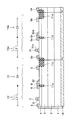
本発明の第1の実施形態に係る窒化物半導体素子について、図1及び図2を参照しながら説明する。図1は第1の実施形態に係る窒化物半導体素子の模式的な断面図であり、図2は該窒化物半導体素子の電極の配置を示す平面図である。
(First embodiment)
A nitride semiconductor device according to a first embodiment of the present invention will be described with reference to FIGS. FIG. 1 is a schematic cross-sectional view of a nitride semiconductor device according to the first embodiment, and FIG. 2 is a plan view showing the arrangement of electrodes of the nitride semiconductor device.
本実施形態に係る窒化物半導体素子は、導電性基板1と、バッファ層2と、窒化物半導体層3と、窒化物半導体層4と、ソース電極5と、ドレイン電極6と、ゲート電極7と、アノード電極8と、カソード電極9と、裏面電極10と、素子分離絶縁層11a,11bと、フレーム電極5Aとを備えている。
The nitride semiconductor device according to this embodiment includes a
図1に示すように、導電性基板1の上にバッファ層2を介してチャネル層となる窒化物半導体層3が形成され、その上にバリア層となる窒化物半導体層4が形成されている。さらに、窒化物半導体層4の上には、HFET(ヘテロ接合電界効果トランジスタ)12のソース電極5、ドレイン電極6及びゲート電極7が形成されるとともに、SBD(ショットキーバリアダイオード)13のアノード電極8及びカソード電極9が形成されている。
As shown in FIG. 1, a
以下、上記の各構成要素について詳しく説明する。 Hereafter, each said component is demonstrated in detail.
導電性基板1は、導電性の基板であり、例えばp型のSi基板であるが、導電型や基板材料はこれに限定されるものではない。即ち、導電性基板1の導電型はn型でもよいし、基板材料としてSiCなど他の材料を用いてもよい。
The
バッファ層2は、導電性基板1の上面に高品質の窒化物半導体層を積層するために設けられる層である。このバッファ層2は、例えばAlGaNからなるが、これに限らず、複数種類の窒化物半導体の薄層を交互に積層した多層構造(AlGaN/GaN,AlN/GaN等)により構成されてもよい。
The
窒化物半導体層(チャネル層)3は、バッファ層2の上に設けられており、ノンドープのAlXGa1−XN(0≦X<1)からなる。なお、窒化物半導体層3はバッファ層2を介さずに導電性基板1の上に直接設けられてもよい。
The nitride semiconductor layer (channel layer) 3 is provided on the
窒化物半導体層(バリア層)4は、窒化物半導体層3の上に設けられており、窒化物半導体層3よりも広いバンドギャップを有する窒化物半導体、例えばAlYGa1−YN(0<Y≦1、X<Y)からなる。
The nitride semiconductor layer (barrier layer) 4 is provided on the
窒化物半導体層4がノンドープの窒化物半導体からなる場合でも、ピエゾ分極により、窒化物半導体層3と窒化物半導体層4との界面には高濃度の二次元電子ガスが発生する。但し、窒化物半導体層4はノンドープに限らず、n型の窒化物半導体からなるようにしてもよい。
Even when the
なお、バリア層となる窒化物半導体層4及びチャネル層となる窒化物半導体層3の材料の組み合わせは、AlGaN/GaN系に限らず、GaN/InGaN系、AlN/AlGaN系、InAlN/GaN系など他の組み合わせでもよい。
Note that the combination of the materials of the
ソース電極5及びドレイン電極6はともに、窒化物半導体層4の上に設けられ、窒化物半導体層4とオーミック接合を形成する。
Both the
また、図2に示すように、ソース電極5及びドレイン電極6は、所定の方向(図2中では縦方向)に沿って交互に複数本設けられる。複数本のソース電極5の一端はいずれもソース電極パッド16に接続されている。また、複数本のドレイン電極6の一端はいずれもドレイン電極/アノード電極パッド17に接続されている。
Further, as shown in FIG. 2, a plurality of
ゲート電極7は、ソース電極5とドレイン電極6の間に設けられ、窒化物半導体層3と窒化物半導体層4との界面に発生する二次元電子ガスの濃度を制御する。このゲート電極7は、図2に示すように、ソース電極5及びドレイン電極6の間に、ソース電極に沿うようにジグザク状に設けられ、その一端がゲート電極パッド18に接続されている。本実施形態では、ゲート電極7は、窒化物半導体層4の上に設けられ、窒化物半導体層4とショットキー接合を形成している。
The
なお、ゲート電極7の構造はショットキーゲートに限らず、いわゆる絶縁ゲート構造を採ってもよい。この場合、ゲート電極7は、窒化物半導体層4の上に形成された絶縁層の上に設けられる。また、本実施形態の第1の変形例で詳しく述べるように、ゲート電極7と窒化物半導体層4の間にp型の窒化物半導体層を介装してもよい。
The structure of the
アノード電極8は、窒化物半導体層4の上に設けられ、窒化物半導体層4とショットキー接合を形成する。また、アノード電極8はドレイン電極6と電気的に接続されている。本実施形態では、図2に示すように、ドレイン電極6及びアノード電極8はドレイン電極/アノード電極パッド17を介して電気的に接続されている。
The
カソード電極9は、窒化物半導体層4の上に設けられ、窒化物半導体層4とオーミック接合を形成する。
The
アノード電極8及びカソード電極9は、図2に示すように、所定の方向に沿って交互に複数本設けられている。複数本のアノード電極8の一端はいずれもドレイン電極/アノード電極パッド17に接続されている。また、複数本のカソード電極9の一端はいずれもカソード電極パッド19に接続されている。
As shown in FIG. 2, a plurality of
フレーム電極5Aは、図2に示すように、HFET12およびSBD13の外周を取り囲む枠状の電極である。フレーム電極5Aは、上記の電極パッド16〜19を含め、HFET12及びSBD13の外周を取り囲むように設けられている。
As shown in FIG. 2, the
また、図2に示すように、フレーム電極5Aは、窒化物半導体層4の上に設けられ、ソース電極5と電気的に接続されるとともに、図1に示すように、導電性基板1とも電気的に接続されている。
As shown in FIG. 2, the
フレーム電極5Aと導電性基板1の電気的接続については各種の手段を採ることができる。図1に示すように、導電性基板1の下面には導電性基板1とオーミック接合を形成するように裏面電極10が設けられている。本実施形態に係る窒化物半導体素子のチップを銅(Cu)などの金属で構成されるパッケージフレームに半田マウントすることにより、裏面電極10はパッケージフレームと電気的に接続される。そして、フレーム電極5Aをパッケージフレームにボンディングワイヤで接続することにより、フレーム電極5Aと導電性基板1とは電気的に接続される。あるいは、窒化物半導体層3及び4を貫通するように設けられたビア(図示せず)によりフレーム電極5Aと導電性基板1とを電気的に接続してもよい。
Various means can be adopted for the electrical connection between the
素子分離絶縁層11aは、図1及び図2からわかるように、ドレイン電極6とアノード電極8の間における窒化物半導体層4の表面から窒化物半導体層3の途中まで設けられている。図2に示すように、素子分離絶縁層11aは、ドレイン電極/アノード電極パッド17を含む領域に形成されている。これにより、SBD13に逆方向電圧が印加されたときに、ドレイン電極6からリーク電流が流れないようにする。即ち、SBD13の逆方向リーク電流を防止する。
As can be seen from FIGS. 1 and 2, the element
素子分離絶縁層11bは、図1及び図2からわかるように、ソース電極5、ソース電極パッド16及びフレーム電極5Aと、カソード電極9及びカソード電極パッド19との間における窒化物半導体層4の表面から窒化物半導体層3の途中まで設けられている。この素子分離絶縁層11bは、ソース電極5、ソース電極パッド16及びフレーム電極5Aと、カソード電極9及びカソード電極パッド19との間に設けられ、両者を絶縁する。
As can be seen from FIGS. 1 and 2, the element
なお、素子分離絶縁層11a及び11bは、その形成プロセスによって限定されるものではなく、例えば、所定の領域にイオン注入を行って形成されたものでもよいし、あるいは、所定の領域にエッチングによりメサを形成したものでもよい。
The element
本実施形態に係る窒化物半導体素子は、機能的には、図1に示すように、ドレイン電極6とアノード電極8を接続するように、HFET12とSBD13を直列接続したものである。図3は、本実施形態に係る窒化物半導体素子を含む昇圧チョッパの回路図を示している。昇圧チョッパ回路は、図3に示すように、HFET12と、このHFET12に直列接続されたSBD13と、キャパシタ14a及び14bと、チョークコイル15とで構成される。図3中破線で囲んだ部分が、本実施形態に係る窒化物半導体素子で構成することのできる部分である。
The nitride semiconductor device according to this embodiment is functionally formed by connecting
上記のように、本実施形態では、HFET12と、このHFET12に直列接続されたSBD13とを集積化することにより、HFET12とSBD13の間の寄生インダクタンスを低減している。
As described above, in this embodiment, the parasitic inductance between the
さらに、本実施形態では、HFET12及びSBD13の外周を取り囲むようにフレーム電極5Aを設ける。このフレーム電極5Aは、昇圧チョッパ回路などの電力変換回路の接地ラインとなるソース電極5と電気的に接続されるとともに、導電性基板1とも電気的に接続される。これにより、接地ラインの寄生インダクタンスを低減している。
Further, in the present embodiment, the
上記のように本実施形態によれば、寄生インダクタンスを低減させることにより、HFET12を高速にスイッチング動作させてもスイッチングノイズの発生を可及的に抑制することができる。
As described above, according to the present embodiment, by reducing the parasitic inductance, it is possible to suppress the occurrence of switching noise as much as possible even when the
さらに、本実施形態では、フレーム電極5AによりHFET12及びSBD13をシールドすることにより、外部からのノイズを遮蔽することができる。
Further, in the present embodiment, noise from the outside can be shielded by shielding the
よって、本実施形態によれば、スイッチングノイズや外部からのノイズを可及的に抑制して、これらのノイズに起因した素子の誤動作を防止し、それにより、誤動作による損失の発生及び素子の破壊を防ぐことができる。 Therefore, according to the present embodiment, switching noise and external noise are suppressed as much as possible to prevent malfunction of the element due to these noises, thereby causing loss due to malfunction and destruction of the element. Can be prevented.
次に、本実施形態による第1ないし第4の変形例について説明する。いずれの変形例も上記効果を得ることができるものである。 Next, first to fourth modifications according to the present embodiment will be described. Any of the modifications can obtain the above effect.
(第1の変形例)
図4は、第1の変形例に係る窒化物半導体素子の模式的な断面図を示している。図4に示すように、本変形例では、ゲート電極7と窒化物半導体層4の間に、p型のAlZGa1−ZN(0≦Z≦1)からなるp型ゲート層31が介装されている。これにより、p型ゲート層31と窒化物半導体層4との界面をビルトインポテンシャルにより空乏化させて、HFET12をノーマリーオフ型にすることができる。
(First modification)
FIG. 4 is a schematic cross-sectional view of the nitride semiconductor device according to the first modification. As shown in FIG. 4, in this modification, a p-
また、本変形例では、図4に示すように、アノード電極8の一部と窒化物半導体層4の間に、p型のAlZGa1−ZN(0≦Z≦1)からなるp型アノード層32が介装されている。これにより、SBD13に過電流を流さなければならない時、p型アノード層32からホールが注入されることにより、急激なオン電圧の上昇を防止することができる。また、SBD13に逆電圧が印加されアバランシェ降伏が起きた場合でも、p型アノード層32から速やかにホールが排出されるため、高いアバランシェ耐量を得ることができる。なお、p型アノード層32は、p型ゲート層31と同時に形成することが可能である。
Further, in this modification, as shown in FIG. 4, p made of p-type Al Z Ga 1-Z N (0 ≦ Z ≦ 1) is formed between a part of the
(第2の変形例)
図5は、第2の変形例に係る窒化物半導体素子の電極の配置を示す平面図を示している。図5に示すように、本変形例では、フレーム電極5Aとドレイン電極6(ドレイン電極/アノード電極パッド17)間の距離Aが、フレーム電極5Aとカソード電極9(カソード電極パッド19)間の距離Bよりも長い。
(Second modification)
FIG. 5 is a plan view showing the arrangement of electrodes of the nitride semiconductor device according to the second modification. As shown in FIG. 5, in this modification, the distance A between the
昇圧チョッパ回路では、ドレイン電極6とアノード電極8との接続点の電位がHFET12のスイッチング動作により変化する。ドレイン電極6とフレーム電極5A間の寄生容量が大きいと、スイッチング動作が遅くなり、回路の損失が増加する。
In the step-up chopper circuit, the potential at the connection point between the
そこで、本変形例では、ドレイン電極6とフレーム電極5A間の距離を、フレーム電極5Aとカソード電極9の距離(B)よりも大きくする。換言すれば、所定の大きさのフレーム電極5Aに対して、その中に配置される各種電極及び電極パッドの位置を、図5の例では右下の方向に寄せている。これにより、ドレイン電極6とフレーム電極5A間の寄生容量を低減させる。その結果、高速スイッチング動作を容易にし、電力変換回路の損失を減らすことができる。
Therefore, in this modification, the distance between the
(第3の変形例)
図6は、第3の変形例に係る窒化物半導体素子の拡大平面図を示している。
(Third Modification)
FIG. 6 is an enlarged plan view of a nitride semiconductor device according to the third modification.
図6に示すように、本変形例では、互いに対向するフレーム電極5Aおよびカソード電極9は、両者の間にジグザグ状の隙間が形成されるように、縁部の形状が加工されている。このジグザグ状の隙間には素子分離絶縁層11bが露出している。
As shown in FIG. 6, in this modification, the
これにより、フレーム電極5Aとカソード電極9との対向面積が大きくなり、両者の間に寄生容量が発生する。この寄生容量は、図3で説明した昇圧チョッパ回路の出力側であるカソード電極9とソース電極5の間に接続される平滑用のキャパシタ14bとして機能させることができる。
As a result, the facing area between the
よって、本変形例によれば、キャパシタ14bを窒化物半導体素子に集積化することが可能となる。
Therefore, according to this modification, the
(第4の変形例)
図7は、第4の変形例に係る窒化物半導体素子の電極の配置を示す平面図である。図7に示すように、本変形例では、ドレイン電極/アノード電極パッド17、ソース電極パッド16及びカソード電極パッド19はフレーム電極5Aの同じ辺(図7の例では下辺)側に配置されている。
(Fourth modification)
FIG. 7 is a plan view showing the arrangement of the electrodes of the nitride semiconductor device according to the fourth modification. As shown in FIG. 7, in this modification, the drain /
図7に示すように、ソース電極5の一端は、ソース電極パッド16に直接又はソース配線20を介して接続されている。また、ドレイン電極6の一端はドレイン電極/アノード電極パッド17に直接又はドレイン配線21を介して接続されている。アノード電極8の一端はドレイン電極/アノード電極パッド17に直接又はアノード配線22を介して接続されている。カソード電極9の一端はカソード電極パッド19に直接又はカソード配線23を介して接続されている。
As shown in FIG. 7, one end of the
ここで、ソース配線20はソース電極5が設けられた層とは別の層に設けられ、ドレイン配線21はドレイン電極6が設けられた層とは別の層に設けられている。また、アノード配線22はアノード電極8が設けられた層とは別の層に設けられ、カソード配線23はカソード電極9が設けられた層とは別の層に設けられている。これらの配線は多層配線技術を用いて形成される。
Here, the
本変形例ではドレイン電極/アノード電極パッド17、ソース電極パッド16及びカソード電極パッド19をフレーム電極5Aの同じ辺側に配置することにより、ソース電極5に流れる電流ISと、ドレイン電極6に流れる電流IDとを逆向きにする。また、アノード電極8に流れる電流IAと、カソード電極9に流れる電流ICとを逆向きにする。これにより、ソース電極5とドレイン電極6のインダクタンスがキャンセルされ、同様に、アノード電極8とカソード電極9のインダクタンスがキャンセルされる。その結果、スイッチングノイズの発生をさらに抑制することができ、高速なスイッチング動作を実現することが可能となる。
By disposing the drain electrode /
(第2の実施形態)
次に、本発明の第2の実施形態に係る窒化物半導体素子について、図8及び図9を参照しながら説明する。図8は第2の実施形態に係る窒化物半導体素子の模式的な断面図であり、図9は該窒化物半導体素子の電極の配置を示す平面図である。
(Second Embodiment)
Next, a nitride semiconductor device according to a second embodiment of the present invention will be described with reference to FIGS. FIG. 8 is a schematic cross-sectional view of a nitride semiconductor device according to the second embodiment, and FIG. 9 is a plan view showing the arrangement of electrodes of the nitride semiconductor device.
第2の実施形態と第1の実施形態との相違点の一つは、第2の実施形態では第2のHFETが形成されている点である。なお、以下の本実施形態の説明において第1の実施形態と同一の構成要素には同一の符号を付して、その説明を省略する。 One of the differences between the second embodiment and the first embodiment is that a second HFET is formed in the second embodiment. In the following description of the present embodiment, the same components as those in the first embodiment are denoted by the same reference numerals, and the description thereof is omitted.
図8に示すように、本実施形態に係る窒化物半導体素子は、HFET12及びSBD13に隣接して設けられたHFET12aをさらに備えている。このHFET12aは、HFET12と類似した構成を有し、ソース電極5aと、ドレイン電極6aと、ゲート電極7aとを有する。
As shown in FIG. 8, the nitride semiconductor device according to this embodiment further includes an
ソース電極5a及びドレイン電極6aはいずれも、窒化物半導体層4の上に設けられ、窒化物半導体層4とオーミック接合を形成する。
Both the
ゲート電極7aは、窒化物半導体層4の上に形成されたp型ゲート層31aの上に設けられている。p型ゲート層31aは、前述のp型ゲート層31と同様、p型のAlZGa1−ZN(0≦Z≦1)からなる。なお、ゲート電極7aは、p型ゲート層31aを介さず、窒化物半導体層4とショットキー接合を形成するように設けてもよい。
図9に示すように、HFET12aのソース電極5aは、ソース電極パッド16a及びフレーム電極5Aを介してHFET12のソース電極5に電気的に接続される。また、ソース電極5aは、素子分離絶縁層11a及び11bによりSBD13と絶縁分離されている。
As shown in FIG. 9, the
図9に示すように、フレーム電極5Aは、HFET12及びSBD13の外周を取り囲むとともに、HFET12aの外周も取り囲む。また、フレーム電極5Aは、HFET12aのソース電極5aにソース電極パッド16aを介して電気的に接続される。
As shown in FIG. 9, the
このソース電極パッド16aにはソース電極5aの一端が電気的に接続される。また、ドレイン電極パッド33にはドレイン電極6aの一端が電気的に接続され、ゲート電極パッド18aにはゲート電極7aの一端が電気的に接続される。
One end of the
素子分離絶縁層11cは、ドレイン電極パッド33を含む領域に設けられ、ドレイン電極パッド33とフレーム電極5Aを絶縁する。
The element
本実施形態に係る窒化物半導体素子を用いることにより、図10に示すようなフライバックコンバータ回路を構成することができる。このフライバックコンバータ回路は、HFET12と、HFET12に直列接続されたSBD13と、キャパシタ14a及び14bと、チョークコイル15と、トランス24と、トランス24の一次側に接続されたHFET12aと、トランス24の二次側に接続されたSBD25と、キャパシタ14cとで構成される。図10中破線で囲んだ部分が、本実施形態に係る窒化物半導体素子で構成することのできる部分である。
By using the nitride semiconductor device according to the present embodiment, a flyback converter circuit as shown in FIG. 10 can be configured. The flyback converter circuit includes an
上記のように、本実施形態では、第1の実施形態の構成に加えて、HFET12のソース電極5と電気的に接続されたソース電極5aを有するHFET12aをさらに備える。また、導電性基板1と電気的に接続されたフレーム電極5Aは、HFET12及びSBD13の外周に加えて、HFET12aの外周も取り囲むように設けられている。これにより、HFET12及び12aのスイッチングノイズの発生を可及的に抑制することができるとともに、外部からのノイズの影響を遮蔽することができる。したがって、低損失かつ高周波動作が可能なフライバックコンバータ回路を提供することができる。
As described above, in this embodiment, in addition to the configuration of the first embodiment, the
(第3の実施形態)
次に、本発明の第3の実施形態に係る窒化物半導体素子について、図11及び図12を参照しながら説明する。図11は第3の実施形態に係る窒化物半導体素子の模式的な断面図であり、図12は該窒化物半導体素子の電極の配置を示す平面図である。
(Third embodiment)
Next, a nitride semiconductor device according to a third embodiment of the present invention will be described with reference to FIGS. FIG. 11 is a schematic cross-sectional view of a nitride semiconductor device according to the third embodiment, and FIG. 12 is a plan view showing the arrangement of electrodes of the nitride semiconductor device.
第3の実施形態と第1の実施形態との相違点の一つは、第3の実施形態では直列接続された第2のHFET及び第2のSBDが形成されている点である。なお、以下の本実施形態の説明において第1及び第2の実施形態と同一の構成要素には同一の符号を付して、その説明を省略する。 One of the differences between the third embodiment and the first embodiment is that a second HFET and a second SBD connected in series are formed in the third embodiment. In the following description of the present embodiment, the same components as those in the first and second embodiments are denoted by the same reference numerals, and the description thereof is omitted.
図11に示すように、本実施形態に係る窒化物半導体素子は、HFET12及びSBD13に隣接して設けられたHFET12a及びSBD13aをさらに備えている。HFET12aは、HFET12と類似した構成を有し、ソース電極5aと、ドレイン電極6aと、ゲート電極7aとを有する。SBD13aは、SBD13と類似した構成を有し、アノード電極8aと、カソード電極9aとを有する。
As shown in FIG. 11, the nitride semiconductor device according to the present embodiment further includes HFETs 12a and SBDs 13a provided adjacent to the
アノード電極8aは、窒化物半導体層4の上に設けられ、窒化物半導体層4とショットキー接合を形成する。また、アノード電極8aは、ドレイン電極HFET12aのドレイン電極6aにドレイン電極/アノード電極パッド17aを介して電気的に接続されている。
The
カソード電極9aは、窒化物半導体層4の上に設けられ、窒化物半導体層4とオーミック接合を形成する。
The
なお、前述の第1の実施形態の第1の変形例と同様に、図11に示すように、アノード電極8aの一部と窒化物半導体層4の間に、p型のAlZGa1−ZN(0≦Z≦1)からなるp型アノード層32aが介装されていてもよい。
Similar to the first modification of the first embodiment described above, as shown in FIG. 11, a p-type Al Z Ga 1 − is formed between a part of the
図12に示すように、フレーム電極5Aは、HFET12及びSBD13の外周を取り囲むとともに、HFET12a及びSBD13aの外周を取り囲む。また、フレーム電極5Aは、HFET12aのソース電極5aにソース電極パッド16aを介して電気的に接続される。
As shown in FIG. 12, the
ドレイン電極/アノード電極パッド17aには、ドレイン電極6aの一端及びアノード電極8aの一端が接続される。カソード電極パッド19aには、カソード電極9aの一端が接続される。
One end of the
素子分離絶縁層11dは、図11及び図12からわかるように、ドレイン電極6aとアノード電極8aの間における窒化物半導体層4の表面から窒化物半導体層3の途中まで設けられている。この素子分離絶縁層11dは、ドレイン電極/アノード電極パッド17aを含む領域に設けられる。これにより、SBD13aの逆方向リーク電流を防止することができる。
As can be seen from FIGS. 11 and 12, the element
素子分離絶縁層11eは、図11及び図12からわかるように、ソース電極5a、ソース電極パッド16a及びフレーム電極5Aと、カソード電極9a及びカソード電極パッド19との間における窒化物半導体層4の表面から窒化物半導体層3の途中まで設けられている。
As can be seen from FIGS. 11 and 12, the element
本実施形態に係る窒化物半導体素子を用いることにより、図13に示すようなフォワードコンバータ回路を構成することができる。このフォワードコンバータ回路は、HFET12と、HFET12に直列接続されたSBD13と、キャパシタ14a及び14bと、チョークコイル15と、トランス24と、トランス24の一次側に接続されたHFET12aと、トランス24の二次側に接続されたSBD25と、キャパシタ14cと、SBD13aと、キャパシタ14dと、抵抗26とで構成される。図13中破線で囲んだ部分が、本実施形態に係る窒化物半導体素子で構成することのできる部分である。
By using the nitride semiconductor device according to this embodiment, a forward converter circuit as shown in FIG. 13 can be configured. This forward converter circuit includes an
上記のように、本実施形態では、第1の実施形態の構成に加えて、直列接続されたHFET12a及びSBD13aをさらに備える。また、導電性基板1と電気的に接続されたフレーム電極5Aは、HFET12及びSBD13の外周に加えて、HFET12a及びSBD13aの外周も取り囲むように設けられている。これにより、HFET12及び12aのスイッチングノイズの発生を可及的に抑制することができるとともに、外部からのノイズの影響を遮蔽することができる。したがって、低損失かつ高周波動作が可能なフォワードコンバータ回路を提供することができる。
As described above, this embodiment further includes the
本発明のいくつかの実施形態を説明したが、これらの実施形態は、例として提示したものであり、発明の範囲を限定することは意図していない。これら実施形態は、その他の様々な形態で実施されることが可能であり、発明の要旨を逸脱しない範囲で、種々の省略、置き換え、変更を行うことができる。これら実施形態やその変形は、発明の範囲や要旨に含まれると同様に、特許請求の範囲に記載された発明とその均等の範囲に含まれるものである。 Although several embodiments of the present invention have been described, these embodiments are presented by way of example and are not intended to limit the scope of the invention. These embodiments can be implemented in various other forms, and various omissions, replacements, and changes can be made without departing from the spirit of the invention. These embodiments and their modifications are included in the scope and gist of the invention, and are also included in the invention described in the claims and the equivalents thereof.
1 導電性基板
2 バッファ層
3 窒化物半導体層(チャネル層)
4 窒化物半導体層(バリア層)
5、5a ソース電極
5A フレーム電極
6、6a ドレイン電極
7,7a ゲート電極
8、8a アノード電極
9、9a カソード電極
10 裏面電極
11a,11b,11c,11d,11e 素子分離絶縁層
12,12a HFET(ヘテロ接合電界効果トランジスタ)
13,13a,25 SBD(ショットキーバリアダイオード)
14a,14b,14c,14d キャパシタ
15 チョークコイル
16,16a ソース電極パッド
17,17a ドレイン電極/アノード電極パッド
18,18a ゲート電極パッド
19,19a カソード電極パッド
20 ソース配線
21 ドレイン配線
22 アノード配線
23 カソード配線
24 トランス
26 抵抗
31,31a p型ゲート層
32,32a p型アノード層
33 ドレイン電極パッド
DESCRIPTION OF
4 Nitride semiconductor layer (barrier layer)
5,
13, 13a, 25 SBD (Schottky barrier diode)
14a, 14b, 14c,
Claims (9)
前記導電性基板の上に直接あるいはバッファ層を介して設けられ、ノンドープの窒化物半導体からなる第1の窒化物半導体層と、
前記第1の窒化物半導体層の上に設けられ、前記第1の窒化物半導体層よりも広いバンドギャップを有するノンドープ又はn型の窒化物半導体からなる第2の窒化物半導体層と、
前記第2の窒化物半導体層の上に設けられ、前記第2の窒化物半導体層とオーミック接合を形成するソース電極と、前記第2の窒化物半導体層の上に設けられ、前記第2の窒化物半導体層とオーミック接合を形成するドレイン電極と、前記ソース電極と前記ドレイン電極の間に設けられ、前記第1の窒化物半導体層と前記第2の窒化物半導体層との界面に発生する二次元電子ガスの濃度を制御するゲート電極と、を有するヘテロ接合電界効果トランジスタと、
前記第2の窒化物半導体層の上に設けられ、前記第2の窒化物半導体層とショットキー接合を形成するとともに、前記ドレイン電極と電気的に接続されたアノード電極と、前記第2の窒化物半導体層の上に設けられ、前記第2の窒化物半導体層とオーミック接合を形成するカソード電極と、を有するショットキーバリアダイオードと、
前記ソース電極及び前記導電性基板と電気的に接続されるとともに、前記第2の窒化物半導体層上に設けられ、前記ソース電極、前記ドレイン電極、前記ゲート電極、前記アノード電極および前記カソード電極を取り囲むフレーム電極と、
前記ドレイン電極と前記フレーム電極との間および前記アノード電極と前記フレーム電極との間において前記第2の窒化物半導体層の表面から前記第1の窒化物半導体層の途中まで設けられ、前記ドレイン電極と前記フレーム電極とを絶縁するとともに前記アノード電極と前記フレーム電極とを絶縁する第1の素子分離絶縁層と、
前記ソース電極と前記カソード電極との間および前記カソード電極と前記フレーム電極との間において前記第2の窒化物半導体層の表面から前記第1の窒化物半導体層の途中まで設けられ、前記ソース電極と前記カソード電極とを絶縁するとともに前記カソード電極と前記フレーム電極とを絶縁する第2の素子分離絶縁層と、
を備えることを特徴とする窒化物半導体素子。 A conductive substrate;
A first nitride semiconductor layer formed on the conductive substrate directly or through a buffer layer and made of a non-doped nitride semiconductor;
A second nitride semiconductor layer formed on the first nitride semiconductor layer and made of a non-doped or n-type nitride semiconductor having a wider band gap than the first nitride semiconductor layer;
A source electrode provided on the second nitride semiconductor layer and forming an ohmic junction with the second nitride semiconductor layer; provided on the second nitride semiconductor layer; A drain electrode that forms an ohmic junction with the nitride semiconductor layer, and is provided between the source electrode and the drain electrode, and is generated at an interface between the first nitride semiconductor layer and the second nitride semiconductor layer. A heterojunction field effect transistor having a gate electrode for controlling the concentration of the two-dimensional electron gas;
An anode electrode provided on the second nitride semiconductor layer to form a Schottky junction with the second nitride semiconductor layer and electrically connected to the drain electrode; and the second nitride A Schottky barrier diode having a cathode electrode provided on the physical semiconductor layer and forming an ohmic junction with the second nitride semiconductor layer;
The source electrode, the drain electrode, the gate electrode, the anode electrode, and the cathode electrode are electrically connected to the source electrode and the conductive substrate and provided on the second nitride semiconductor layer. Surrounding frame electrodes;
The drain electrode is provided between the drain electrode and the frame electrode and between the anode electrode and the frame electrode, from the surface of the second nitride semiconductor layer to the middle of the first nitride semiconductor layer. A first element isolation insulating layer that insulates the frame electrode and the anode electrode from the frame electrode ;
Provided between the source electrode and the cathode electrode and between the cathode electrode and the frame electrode from the surface of the second nitride semiconductor layer to the middle of the first nitride semiconductor layer, A second element isolation insulating layer that insulates the cathode electrode from the cathode electrode and the frame electrode ;
A nitride semiconductor device comprising:
前記アノード電極と前記カソード電極は所定の方向に沿って交互に複数本設けられるとともに、前記アノード電極の一端は前記ドレイン電極/アノード電極パッドに直接又は前記アノード電極が設けられた層とは別の層に設けられたアノード配線を介して接続され、前記カソード電極の一端はカソード電極パッドに直接又は前記カソード電極が設けられた層とは別の層に設けられたカソード配線を介して接続され、
前記ドレイン電極/アノード電極パッド、前記ソース電極パッド、及び前記カソード電極パッドは前記フレーム電極の同じ辺側に配置されていることを特徴とする請求項1乃至6のいずれかに記載の窒化物半導体素子。 A plurality of the source electrodes and the drain electrodes are alternately provided along a predetermined direction, and one end of the source electrode is provided directly on the source electrode pad or on a layer different from the layer on which the source electrode is provided. One end of the drain electrode is connected to the drain electrode / anode electrode pad directly or via a drain wiring provided in a layer different from the layer in which the drain electrode is provided,
A plurality of the anode electrodes and the cathode electrodes are alternately provided along a predetermined direction, and one end of the anode electrode is provided directly on the drain electrode / anode electrode pad or different from the layer on which the anode electrode is provided. Connected via an anode wiring provided in a layer, one end of the cathode electrode is connected directly to a cathode electrode pad or via a cathode wiring provided in a layer different from the layer provided with the cathode electrode,
The drain electrode / anode electrode pad, the source electrode pad, and the cathode electrode pad nitride semiconductor according to any of claims 1 to 6, characterized in that arranged on the same side of the frame electrode element.
前記フレーム電極は、前記別のヘテロ接合電界効果トランジスタの外周を取り囲むとともに、前記別のヘテロ接合電界効果トランジスタのソース電極と電気的に接続されることを特徴とする請求項1乃至7のいずれかに記載の窒化物半導体素子。 A heterojunction field effect transistor different from the heterojunction field effect transistor;
The frame electrode surrounds the outer periphery of the further heterojunction field effect transistor, any one of claims 1 to 7, characterized in that it is the further connection of the source electrode and the electrically heterojunction field effect transistor The nitride semiconductor device described in 1.
前記別のヘテロ接合電界効果トランジスタのドレイン電極と電気的に接続されたアノード電極を有する、前記ショットキーバリアダイオードとは別のショットキーバリアダイオードと、をさらに備え、
前記フレーム電極は、前記別のヘテロ接合電界効果トランジスタ及び前記別のショットキーバリアダイオードの外周を取り囲むとともに、前記別のヘテロ接合電界効果トランジスタのソース電極と電気的に接続されることを特徴とする請求項1乃至7のいずれかに記載の窒化物半導体素子。 A heterojunction field effect transistor different from the heterojunction field effect transistor;
A Schottky barrier diode different from the Schottky barrier diode having an anode electrode electrically connected to a drain electrode of the another heterojunction field effect transistor;
The frame electrode surrounds an outer periphery of the another heterojunction field effect transistor and the another Schottky barrier diode, and is electrically connected to a source electrode of the another heterojunction field effect transistor. The nitride semiconductor device according to claim 1 .
Priority Applications (4)
| Application Number | Priority Date | Filing Date | Title |
|---|---|---|---|
| JP2012068143A JP5659182B2 (en) | 2012-03-23 | 2012-03-23 | Nitride semiconductor device |
| US13/599,951 US8581301B2 (en) | 2012-03-23 | 2012-08-30 | Nitride semiconductor device |
| CN201210315907.8A CN103325828B (en) | 2012-03-23 | 2012-08-30 | Nitride semiconductor device |
| US14/048,480 US8928039B2 (en) | 2012-03-23 | 2013-10-08 | Semiconductor device including heterojunction field effect transistor and Schottky barrier diode |
Applications Claiming Priority (1)
| Application Number | Priority Date | Filing Date | Title |
|---|---|---|---|
| JP2012068143A JP5659182B2 (en) | 2012-03-23 | 2012-03-23 | Nitride semiconductor device |
Publications (2)
| Publication Number | Publication Date |
|---|---|
| JP2013201242A JP2013201242A (en) | 2013-10-03 |
| JP5659182B2 true JP5659182B2 (en) | 2015-01-28 |
Family
ID=49194481
Family Applications (1)
| Application Number | Title | Priority Date | Filing Date |
|---|---|---|---|
| JP2012068143A Active JP5659182B2 (en) | 2012-03-23 | 2012-03-23 | Nitride semiconductor device |
Country Status (3)
| Country | Link |
|---|---|
| US (2) | US8581301B2 (en) |
| JP (1) | JP5659182B2 (en) |
| CN (1) | CN103325828B (en) |
Families Citing this family (27)
| Publication number | Priority date | Publication date | Assignee | Title |
|---|---|---|---|---|
| JP5659182B2 (en) * | 2012-03-23 | 2015-01-28 | 株式会社東芝 | Nitride semiconductor device |
| KR101395026B1 (en) * | 2012-10-16 | 2014-05-15 | 경북대학교 산학협력단 | Nitride Semiconductor and Fabricating Method Thereof |
| KR102182016B1 (en) * | 2013-12-02 | 2020-11-23 | 엘지이노텍 주식회사 | Semiconductor device and semiconductor circuit including the device |
| KR101758082B1 (en) * | 2013-12-30 | 2017-07-17 | 한국전자통신연구원 | Methods of manufacturing nitride semiconductor devices |
| JP2015177016A (en) * | 2014-03-14 | 2015-10-05 | 株式会社東芝 | Semiconductor device |
| US9893603B2 (en) * | 2014-06-06 | 2018-02-13 | Hitachi Automotive Systems, Ltd. | Power converter |
| JP6347685B2 (en) * | 2014-07-08 | 2018-06-27 | ルネサスエレクトロニクス株式会社 | Semiconductor device |
| CN104201253B (en) * | 2014-07-10 | 2017-08-25 | 中航(重庆)微电子有限公司 | A kind of gallium nitride device and its manufacture method |
| JP6055799B2 (en) | 2014-07-29 | 2016-12-27 | 株式会社豊田中央研究所 | Semiconductor device and manufacturing method thereof |
| US9537338B2 (en) | 2014-09-16 | 2017-01-03 | Navitas Semiconductor Inc. | Level shift and inverter circuits for GaN devices |
| US9571093B2 (en) | 2014-09-16 | 2017-02-14 | Navitas Semiconductor, Inc. | Half bridge driver circuits |
| US9960154B2 (en) * | 2014-09-19 | 2018-05-01 | Navitas Semiconductor, Inc. | GaN structures |
| US10153276B2 (en) | 2014-12-17 | 2018-12-11 | Infineon Technologies Austria Ag | Group III heterojunction semiconductor device having silicon carbide-containing lateral diode |
| JP6584783B2 (en) * | 2015-02-06 | 2019-10-02 | ルネサスエレクトロニクス株式会社 | Semiconductor device |
| JP2016171197A (en) * | 2015-03-12 | 2016-09-23 | 株式会社東芝 | Semiconductor device |
| DE102015208150A1 (en) * | 2015-05-04 | 2016-11-10 | Robert Bosch Gmbh | Method for producing an electronic circuit device and electronic circuit device |
| JP6552925B2 (en) | 2015-09-04 | 2019-07-31 | 株式会社東芝 | Semiconductor device |
| US9831867B1 (en) | 2016-02-22 | 2017-11-28 | Navitas Semiconductor, Inc. | Half bridge driver circuits |
| CN107845630A (en) * | 2017-10-24 | 2018-03-27 | 电子科技大学 | GaN base single-chip integration formula half-bridge circuit |
| FR3097682B1 (en) * | 2019-06-19 | 2023-01-13 | St Microelectronics Gmbh | Monolithic component comprising a gallium nitride power transistor |
| WO2021085558A1 (en) * | 2019-10-30 | 2021-05-06 | パナソニックIpマネジメント株式会社 | Semiconductor device |
| TW202207600A (en) * | 2020-07-10 | 2022-02-16 | 日商Flosfia股份有限公司 | Power conversion circuit and power conversion system |
| US12068408B2 (en) * | 2020-07-15 | 2024-08-20 | Semiconductor Components Industries, Llc | High electron mobility transistor |
| CN112903755B (en) * | 2021-02-24 | 2023-06-02 | 太原理工大学 | Carbon dioxide sensor and preparation method thereof |
| CN113644115B (en) * | 2021-08-09 | 2023-03-21 | 西安电子科技大学 | Anti-radiation FDSOI field effect transistor based on 22nm technology and preparation method thereof |
| CN114823849A (en) * | 2022-04-15 | 2022-07-29 | 晶通半导体(深圳)有限公司 | Gallium Nitride Reverse Blocking Transistor |
| CN118016665B (en) * | 2024-04-10 | 2024-06-11 | 山东大学 | Enhancement-mode GaN HEMT on SiC substrate with integrated SBD |
Family Cites Families (33)
| Publication number | Priority date | Publication date | Assignee | Title |
|---|---|---|---|---|
| US4017A (en) * | 1845-05-01 | Reid r | ||
| US10001A (en) * | 1853-09-06 | Straw-cutter | ||
| US6027A (en) * | 1849-01-09 | Rotary blacksmith s twyer | ||
| JPH04324981A (en) * | 1991-04-25 | 1992-11-13 | Hitachi Ltd | Forming method of compound semiconductor integrated circuit device |
| JPH0758126A (en) * | 1993-08-11 | 1995-03-03 | Sony Corp | Compound semiconductor integrated circuit |
| JP3287279B2 (en) * | 1997-09-25 | 2002-06-04 | 日本電気株式会社 | Semiconductor chip and semiconductor device on which the semiconductor chip is mounted |
| JP3292175B2 (en) * | 1999-05-13 | 2002-06-17 | 日本電気株式会社 | Semiconductor device |
| JP5130641B2 (en) | 2006-03-31 | 2013-01-30 | サンケン電気株式会社 | Composite semiconductor device |
| JP4177048B2 (en) | 2001-11-27 | 2008-11-05 | 古河電気工業株式会社 | Power converter and GaN-based semiconductor device used therefor |
| CN100388509C (en) | 2003-01-29 | 2008-05-14 | 株式会社东芝 | power semiconductor device |
| US6933544B2 (en) | 2003-01-29 | 2005-08-23 | Kabushiki Kaisha Toshiba | Power semiconductor device |
| JP4190931B2 (en) | 2003-03-28 | 2008-12-03 | 三菱電機株式会社 | Semiconductor device |
| JP2005149761A (en) * | 2003-11-11 | 2005-06-09 | Sony Corp | Power supply device for generating plasma |
| JP4810072B2 (en) * | 2004-06-15 | 2011-11-09 | 株式会社東芝 | Nitrogen compound-containing semiconductor devices |
| JP2006100645A (en) | 2004-09-30 | 2006-04-13 | Furukawa Electric Co Ltd:The | GaN-based semiconductor integrated circuit |
| US7208785B2 (en) * | 2004-12-20 | 2007-04-24 | Silicon-Based Technology Corp. | Self-aligned Schottky-barrier clamped planar DMOS transistor structure and its manufacturing methods |
| JP2006222298A (en) * | 2005-02-10 | 2006-08-24 | Renesas Technology Corp | Semiconductor device and manufacturing method thereof |
| JP5319084B2 (en) | 2007-06-19 | 2013-10-16 | ルネサスエレクトロニクス株式会社 | Semiconductor device |
| JP4478175B2 (en) | 2007-06-26 | 2010-06-09 | 株式会社東芝 | Semiconductor device |
| US8703605B2 (en) * | 2007-12-18 | 2014-04-22 | Byung Chun Yang | High yield and high throughput method for the manufacture of integrated circuit devices of improved integrity, performance and reliability |
| JP5369434B2 (en) * | 2007-12-21 | 2013-12-18 | サンケン電気株式会社 | Bidirectional switch |
| JP2009164158A (en) | 2007-12-28 | 2009-07-23 | Panasonic Corp | Semiconductor device and manufacturing method thereof |
| JP5439725B2 (en) * | 2008-02-20 | 2014-03-12 | サンケン電気株式会社 | Semiconductor switching device |
| JP5526496B2 (en) * | 2008-06-02 | 2014-06-18 | サンケン電気株式会社 | Field effect semiconductor device and manufacturing method thereof |
| US8390091B2 (en) * | 2009-02-03 | 2013-03-05 | Freescale Semiconductor, Inc. | Semiconductor structure, an integrated circuit including a semiconductor structure and a method for manufacturing a semiconductor structure |
| JP5017303B2 (en) * | 2009-03-25 | 2012-09-05 | 株式会社東芝 | Semiconductor device |
| JP4700125B2 (en) | 2009-07-30 | 2011-06-15 | 住友電気工業株式会社 | Semiconductor device and manufacturing method thereof |
| WO2011064955A1 (en) | 2009-11-30 | 2011-06-03 | パナソニック株式会社 | Bidirectional switch |
| JP2011165749A (en) * | 2010-02-05 | 2011-08-25 | Panasonic Corp | Semiconductor device |
| KR101148694B1 (en) * | 2010-12-09 | 2012-05-25 | 삼성전기주식회사 | Nitride based semiconductor device and method for manufacturing the same |
| JP2011135094A (en) | 2011-02-25 | 2011-07-07 | Sumitomo Electric Ind Ltd | Semiconductor device, and method of manufacturing the same |
| KR20120120829A (en) * | 2011-04-25 | 2012-11-02 | 삼성전기주식회사 | Nitride semiconductor device and manufacturing method thereof |
| JP5659182B2 (en) * | 2012-03-23 | 2015-01-28 | 株式会社東芝 | Nitride semiconductor device |
-
2012
- 2012-03-23 JP JP2012068143A patent/JP5659182B2/en active Active
- 2012-08-30 CN CN201210315907.8A patent/CN103325828B/en not_active Expired - Fee Related
- 2012-08-30 US US13/599,951 patent/US8581301B2/en not_active Expired - Fee Related
-
2013
- 2013-10-08 US US14/048,480 patent/US8928039B2/en active Active
Also Published As
| Publication number | Publication date |
|---|---|
| CN103325828A (en) | 2013-09-25 |
| US8928039B2 (en) | 2015-01-06 |
| US20130248931A1 (en) | 2013-09-26 |
| CN103325828B (en) | 2016-03-23 |
| US8581301B2 (en) | 2013-11-12 |
| JP2013201242A (en) | 2013-10-03 |
| US20140035004A1 (en) | 2014-02-06 |
Similar Documents
| Publication | Publication Date | Title |
|---|---|---|
| JP5659182B2 (en) | Nitride semiconductor device | |
| US8203172B2 (en) | Nitride semiconductor device | |
| JP5548909B2 (en) | Nitride semiconductor device | |
| JP4645313B2 (en) | Semiconductor device | |
| US9654001B2 (en) | Semiconductor device | |
| JP5883799B2 (en) | Electronic devices and components for high efficiency power circuits | |
| JP5672756B2 (en) | Semiconductor device | |
| US7884394B2 (en) | III-nitride devices and circuits | |
| KR101539531B1 (en) | Semiconductor device | |
| JP5530682B2 (en) | Nitride semiconductor device | |
| CN102460709A (en) | power conversion device | |
| JP2013058640A (en) | Semiconductor device | |
| JP2022525654A (en) | Integrated design for Group III nitride devices | |
| JP2006269586A (en) | Semiconductor element | |
| WO2019003746A1 (en) | SEMICONDUCTOR DEVICE | |
| JP2018056506A (en) | Semiconductor device | |
| JP6562359B2 (en) | Semiconductor device | |
| JP2014078570A (en) | Rectifier circuit and semiconductor device | |
| JP2007180143A (en) | Nitride semiconductor element | |
| JP6331471B2 (en) | Nitride semiconductor device | |
| JP5985162B2 (en) | Nitride semiconductor device | |
| JP2015177218A (en) | Switching power supply | |
| JP2013041976A (en) | Nitride semiconductor device | |
| WO2025046981A1 (en) | Nitride semiconductor device | |
| JP6216559B2 (en) | Compound semiconductor device and manufacturing method thereof |
Legal Events
| Date | Code | Title | Description |
|---|---|---|---|
| A621 | Written request for application examination |
Free format text: JAPANESE INTERMEDIATE CODE: A621 Effective date: 20140206 |
|
| A131 | Notification of reasons for refusal |
Free format text: JAPANESE INTERMEDIATE CODE: A131 Effective date: 20140527 |
|
| A977 | Report on retrieval |
Free format text: JAPANESE INTERMEDIATE CODE: A971007 Effective date: 20140530 |
|
| A521 | Request for written amendment filed |
Free format text: JAPANESE INTERMEDIATE CODE: A523 Effective date: 20140728 |
|
| TRDD | Decision of grant or rejection written | ||
| A01 | Written decision to grant a patent or to grant a registration (utility model) |
Free format text: JAPANESE INTERMEDIATE CODE: A01 Effective date: 20141104 |
|
| A61 | First payment of annual fees (during grant procedure) |
Free format text: JAPANESE INTERMEDIATE CODE: A61 Effective date: 20141201 |
|
| R151 | Written notification of patent or utility model registration |
Ref document number: 5659182 Country of ref document: JP Free format text: JAPANESE INTERMEDIATE CODE: R151 |