JP5659182B2 - 窒化物半導体素子 - Google Patents
窒化物半導体素子 Download PDFInfo
- Publication number
- JP5659182B2 JP5659182B2 JP2012068143A JP2012068143A JP5659182B2 JP 5659182 B2 JP5659182 B2 JP 5659182B2 JP 2012068143 A JP2012068143 A JP 2012068143A JP 2012068143 A JP2012068143 A JP 2012068143A JP 5659182 B2 JP5659182 B2 JP 5659182B2
- Authority
- JP
- Japan
- Prior art keywords
- electrode
- nitride semiconductor
- semiconductor layer
- layer
- anode
- Prior art date
- Legal status (The legal status is an assumption and is not a legal conclusion. Google has not performed a legal analysis and makes no representation as to the accuracy of the status listed.)
- Active
Links
Images


Classifications
-
- H—ELECTRICITY
- H10—SEMICONDUCTOR DEVICES; ELECTRIC SOLID-STATE DEVICES NOT OTHERWISE PROVIDED FOR
- H10D—INORGANIC ELECTRIC SEMICONDUCTOR DEVICES
- H10D84/00—Integrated devices formed in or on semiconductor substrates that comprise only semiconducting layers, e.g. on Si wafers or on GaAs-on-Si wafers
- H10D84/01—Manufacture or treatment
- H10D84/02—Manufacture or treatment characterised by using material-based technologies
- H10D84/05—Manufacture or treatment characterised by using material-based technologies using Group III-V technology
-
- H—ELECTRICITY
- H02—GENERATION; CONVERSION OR DISTRIBUTION OF ELECTRIC POWER
- H02M—APPARATUS FOR CONVERSION BETWEEN AC AND AC, BETWEEN AC AND DC, OR BETWEEN DC AND DC, AND FOR USE WITH MAINS OR SIMILAR POWER SUPPLY SYSTEMS; CONVERSION OF DC OR AC INPUT POWER INTO SURGE OUTPUT POWER; CONTROL OR REGULATION THEREOF
- H02M3/00—Conversion of DC power input into DC power output
- H02M3/02—Conversion of DC power input into DC power output without intermediate conversion into AC
- H02M3/04—Conversion of DC power input into DC power output without intermediate conversion into AC by static converters
- H02M3/10—Conversion of DC power input into DC power output without intermediate conversion into AC by static converters using discharge tubes with control electrode or semiconductor devices with control electrode
- H02M3/145—Conversion of DC power input into DC power output without intermediate conversion into AC by static converters using discharge tubes with control electrode or semiconductor devices with control electrode using devices of a triode or transistor type requiring continuous application of a control signal
- H02M3/155—Conversion of DC power input into DC power output without intermediate conversion into AC by static converters using discharge tubes with control electrode or semiconductor devices with control electrode using devices of a triode or transistor type requiring continuous application of a control signal using semiconductor devices only
- H02M3/156—Conversion of DC power input into DC power output without intermediate conversion into AC by static converters using discharge tubes with control electrode or semiconductor devices with control electrode using devices of a triode or transistor type requiring continuous application of a control signal using semiconductor devices only with automatic control of output voltage or current, e.g. switching regulators
-
- H—ELECTRICITY
- H10—SEMICONDUCTOR DEVICES; ELECTRIC SOLID-STATE DEVICES NOT OTHERWISE PROVIDED FOR
- H10D—INORGANIC ELECTRIC SEMICONDUCTOR DEVICES
- H10D30/00—Field-effect transistors [FET]
- H10D30/40—FETs having zero-dimensional [0D], one-dimensional [1D] or two-dimensional [2D] charge carrier gas channels
- H10D30/47—FETs having zero-dimensional [0D], one-dimensional [1D] or two-dimensional [2D] charge carrier gas channels having 2D charge carrier gas channels, e.g. nanoribbon FETs or high electron mobility transistors [HEMT]
- H10D30/471—High electron mobility transistors [HEMT] or high hole mobility transistors [HHMT]
- H10D30/475—High electron mobility transistors [HEMT] or high hole mobility transistors [HHMT] having wider bandgap layer formed on top of lower bandgap active layer, e.g. undoped barrier HEMTs such as i-AlGaN/GaN HEMTs
-
- H—ELECTRICITY
- H10—SEMICONDUCTOR DEVICES; ELECTRIC SOLID-STATE DEVICES NOT OTHERWISE PROVIDED FOR
- H10D—INORGANIC ELECTRIC SEMICONDUCTOR DEVICES
- H10D8/00—Diodes
- H10D8/60—Schottky-barrier diodes
-
- H—ELECTRICITY
- H10—SEMICONDUCTOR DEVICES; ELECTRIC SOLID-STATE DEVICES NOT OTHERWISE PROVIDED FOR
- H10D—INORGANIC ELECTRIC SEMICONDUCTOR DEVICES
- H10D84/00—Integrated devices formed in or on semiconductor substrates that comprise only semiconducting layers, e.g. on Si wafers or on GaAs-on-Si wafers
- H10D84/01—Manufacture or treatment
-
- H—ELECTRICITY
- H10—SEMICONDUCTOR DEVICES; ELECTRIC SOLID-STATE DEVICES NOT OTHERWISE PROVIDED FOR
- H10D—INORGANIC ELECTRIC SEMICONDUCTOR DEVICES
- H10D84/00—Integrated devices formed in or on semiconductor substrates that comprise only semiconducting layers, e.g. on Si wafers or on GaAs-on-Si wafers
- H10D84/80—Integrated devices formed in or on semiconductor substrates that comprise only semiconducting layers, e.g. on Si wafers or on GaAs-on-Si wafers characterised by the integration of at least one component covered by groups H10D12/00 or H10D30/00, e.g. integration of IGFETs
- H10D84/811—Combinations of field-effect devices and one or more diodes, capacitors or resistors
-
- H—ELECTRICITY
- H10—SEMICONDUCTOR DEVICES; ELECTRIC SOLID-STATE DEVICES NOT OTHERWISE PROVIDED FOR
- H10D—INORGANIC ELECTRIC SEMICONDUCTOR DEVICES
- H10D89/00—Aspects of integrated devices not covered by groups H10D84/00 - H10D88/00
- H10D89/10—Integrated device layouts
-
- H—ELECTRICITY
- H01—ELECTRIC ELEMENTS
- H01L—SEMICONDUCTOR DEVICES NOT COVERED BY CLASS H10
- H01L2924/00—Indexing scheme for arrangements or methods for connecting or disconnecting semiconductor or solid-state bodies as covered by H01L24/00
- H01L2924/0001—Technical content checked by a classifier
- H01L2924/0002—Not covered by any one of groups H01L24/00, H01L24/00 and H01L2224/00
-
- H—ELECTRICITY
- H02—GENERATION; CONVERSION OR DISTRIBUTION OF ELECTRIC POWER
- H02M—APPARATUS FOR CONVERSION BETWEEN AC AND AC, BETWEEN AC AND DC, OR BETWEEN DC AND DC, AND FOR USE WITH MAINS OR SIMILAR POWER SUPPLY SYSTEMS; CONVERSION OF DC OR AC INPUT POWER INTO SURGE OUTPUT POWER; CONTROL OR REGULATION THEREOF
- H02M1/00—Details of apparatus for conversion
- H02M1/0067—Converter structures employing plural converter units, other than for parallel operation of the units on a single load
- H02M1/007—Plural converter units in cascade
-
- H—ELECTRICITY
- H02—GENERATION; CONVERSION OR DISTRIBUTION OF ELECTRIC POWER
- H02M—APPARATUS FOR CONVERSION BETWEEN AC AND AC, BETWEEN AC AND DC, OR BETWEEN DC AND DC, AND FOR USE WITH MAINS OR SIMILAR POWER SUPPLY SYSTEMS; CONVERSION OF DC OR AC INPUT POWER INTO SURGE OUTPUT POWER; CONTROL OR REGULATION THEREOF
- H02M3/00—Conversion of DC power input into DC power output
- H02M3/02—Conversion of DC power input into DC power output without intermediate conversion into AC
- H02M3/04—Conversion of DC power input into DC power output without intermediate conversion into AC by static converters
- H02M3/10—Conversion of DC power input into DC power output without intermediate conversion into AC by static converters using discharge tubes with control electrode or semiconductor devices with control electrode
- H02M3/145—Conversion of DC power input into DC power output without intermediate conversion into AC by static converters using discharge tubes with control electrode or semiconductor devices with control electrode using devices of a triode or transistor type requiring continuous application of a control signal
- H02M3/155—Conversion of DC power input into DC power output without intermediate conversion into AC by static converters using discharge tubes with control electrode or semiconductor devices with control electrode using devices of a triode or transistor type requiring continuous application of a control signal using semiconductor devices only
-
- H—ELECTRICITY
- H02—GENERATION; CONVERSION OR DISTRIBUTION OF ELECTRIC POWER
- H02M—APPARATUS FOR CONVERSION BETWEEN AC AND AC, BETWEEN AC AND DC, OR BETWEEN DC AND DC, AND FOR USE WITH MAINS OR SIMILAR POWER SUPPLY SYSTEMS; CONVERSION OF DC OR AC INPUT POWER INTO SURGE OUTPUT POWER; CONTROL OR REGULATION THEREOF
- H02M3/00—Conversion of DC power input into DC power output
- H02M3/22—Conversion of DC power input into DC power output with intermediate conversion into AC
- H02M3/24—Conversion of DC power input into DC power output with intermediate conversion into AC by static converters
- H02M3/28—Conversion of DC power input into DC power output with intermediate conversion into AC by static converters using discharge tubes with control electrode or semiconductor devices with control electrode to produce the intermediate AC
- H02M3/325—Conversion of DC power input into DC power output with intermediate conversion into AC by static converters using discharge tubes with control electrode or semiconductor devices with control electrode to produce the intermediate AC using devices of a triode or a transistor type requiring continuous application of a control signal
- H02M3/335—Conversion of DC power input into DC power output with intermediate conversion into AC by static converters using discharge tubes with control electrode or semiconductor devices with control electrode to produce the intermediate AC using devices of a triode or a transistor type requiring continuous application of a control signal using semiconductor devices only
- H02M3/33569—Conversion of DC power input into DC power output with intermediate conversion into AC by static converters using discharge tubes with control electrode or semiconductor devices with control electrode to produce the intermediate AC using devices of a triode or a transistor type requiring continuous application of a control signal using semiconductor devices only having several active switching elements
-
- H—ELECTRICITY
- H10—SEMICONDUCTOR DEVICES; ELECTRIC SOLID-STATE DEVICES NOT OTHERWISE PROVIDED FOR
- H10D—INORGANIC ELECTRIC SEMICONDUCTOR DEVICES
- H10D62/00—Semiconductor bodies, or regions thereof, of devices having potential barriers
- H10D62/10—Shapes, relative sizes or dispositions of the regions of the semiconductor bodies; Shapes of the semiconductor bodies
- H10D62/102—Constructional design considerations for preventing surface leakage or controlling electric field concentration
- H10D62/103—Constructional design considerations for preventing surface leakage or controlling electric field concentration for increasing or controlling the breakdown voltage of reverse-biased devices
- H10D62/105—Constructional design considerations for preventing surface leakage or controlling electric field concentration for increasing or controlling the breakdown voltage of reverse-biased devices by having particular doping profiles, shapes or arrangements of PN junctions; by having supplementary regions, e.g. junction termination extension [JTE]
- H10D62/106—Constructional design considerations for preventing surface leakage or controlling electric field concentration for increasing or controlling the breakdown voltage of reverse-biased devices by having particular doping profiles, shapes or arrangements of PN junctions; by having supplementary regions, e.g. junction termination extension [JTE] having supplementary regions doped oppositely to or in rectifying contact with regions of the semiconductor bodies, e.g. guard rings with PN or Schottky junctions
-
- H—ELECTRICITY
- H10—SEMICONDUCTOR DEVICES; ELECTRIC SOLID-STATE DEVICES NOT OTHERWISE PROVIDED FOR
- H10D—INORGANIC ELECTRIC SEMICONDUCTOR DEVICES
- H10D62/00—Semiconductor bodies, or regions thereof, of devices having potential barriers
- H10D62/10—Shapes, relative sizes or dispositions of the regions of the semiconductor bodies; Shapes of the semiconductor bodies
- H10D62/17—Semiconductor regions connected to electrodes not carrying current to be rectified, amplified or switched, e.g. channel regions
- H10D62/343—Gate regions of field-effect devices having PN junction gates
-
- H—ELECTRICITY
- H10—SEMICONDUCTOR DEVICES; ELECTRIC SOLID-STATE DEVICES NOT OTHERWISE PROVIDED FOR
- H10D—INORGANIC ELECTRIC SEMICONDUCTOR DEVICES
- H10D62/00—Semiconductor bodies, or regions thereof, of devices having potential barriers
- H10D62/80—Semiconductor bodies, or regions thereof, of devices having potential barriers characterised by the materials
- H10D62/85—Semiconductor bodies, or regions thereof, of devices having potential barriers characterised by the materials being Group III-V materials, e.g. GaAs
- H10D62/8503—Nitride Group III-V materials, e.g. AlN or GaN
-
- H—ELECTRICITY
- H10—SEMICONDUCTOR DEVICES; ELECTRIC SOLID-STATE DEVICES NOT OTHERWISE PROVIDED FOR
- H10D—INORGANIC ELECTRIC SEMICONDUCTOR DEVICES
- H10D64/00—Electrodes of devices having potential barriers
- H10D64/20—Electrodes characterised by their shapes, relative sizes or dispositions
- H10D64/23—Electrodes carrying the current to be rectified, amplified, oscillated or switched, e.g. sources, drains, anodes or cathodes
- H10D64/251—Source or drain electrodes for field-effect devices
- H10D64/257—Source or drain electrodes for field-effect devices for lateral devices wherein the source or drain electrodes are characterised by top-view geometrical layouts, e.g. interdigitated, semi-circular, annular or L-shaped electrodes
Landscapes
- Engineering & Computer Science (AREA)
- Power Engineering (AREA)
- Junction Field-Effect Transistors (AREA)
- Electrodes Of Semiconductors (AREA)
- Internal Circuitry In Semiconductor Integrated Circuit Devices (AREA)
- Semiconductor Integrated Circuits (AREA)
Description
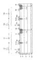
本発明の第1の実施形態に係る窒化物半導体素子について、図1及び図2を参照しながら説明する。図1は第1の実施形態に係る窒化物半導体素子の模式的な断面図であり、図2は該窒化物半導体素子の電極の配置を示す平面図である。
図4は、第1の変形例に係る窒化物半導体素子の模式的な断面図を示している。図4に示すように、本変形例では、ゲート電極7と窒化物半導体層4の間に、p型のAlZGa1−ZN(0≦Z≦1)からなるp型ゲート層31が介装されている。これにより、p型ゲート層31と窒化物半導体層4との界面をビルトインポテンシャルにより空乏化させて、HFET12をノーマリーオフ型にすることができる。
図5は、第2の変形例に係る窒化物半導体素子の電極の配置を示す平面図を示している。図5に示すように、本変形例では、フレーム電極5Aとドレイン電極6(ドレイン電極/アノード電極パッド17)間の距離Aが、フレーム電極5Aとカソード電極9(カソード電極パッド19)間の距離Bよりも長い。
図6は、第3の変形例に係る窒化物半導体素子の拡大平面図を示している。
図7は、第4の変形例に係る窒化物半導体素子の電極の配置を示す平面図である。図7に示すように、本変形例では、ドレイン電極/アノード電極パッド17、ソース電極パッド16及びカソード電極パッド19はフレーム電極5Aの同じ辺(図7の例では下辺)側に配置されている。
次に、本発明の第2の実施形態に係る窒化物半導体素子について、図8及び図9を参照しながら説明する。図8は第2の実施形態に係る窒化物半導体素子の模式的な断面図であり、図9は該窒化物半導体素子の電極の配置を示す平面図である。
次に、本発明の第3の実施形態に係る窒化物半導体素子について、図11及び図12を参照しながら説明する。図11は第3の実施形態に係る窒化物半導体素子の模式的な断面図であり、図12は該窒化物半導体素子の電極の配置を示す平面図である。
2 バッファ層
3 窒化物半導体層(チャネル層)
4 窒化物半導体層(バリア層)
5、5a ソース電極
5A フレーム電極
6、6a ドレイン電極
7,7a ゲート電極
8、8a アノード電極
9、9a カソード電極
10 裏面電極
11a,11b,11c,11d,11e 素子分離絶縁層
12,12a HFET(ヘテロ接合電界効果トランジスタ)
13,13a,25 SBD(ショットキーバリアダイオード)
14a,14b,14c,14d キャパシタ
15 チョークコイル
16,16a ソース電極パッド
17,17a ドレイン電極/アノード電極パッド
18,18a ゲート電極パッド
19,19a カソード電極パッド
20 ソース配線
21 ドレイン配線
22 アノード配線
23 カソード配線
24 トランス
26 抵抗
31,31a p型ゲート層
32,32a p型アノード層
33 ドレイン電極パッド
Claims (9)
- 導電性基板と、
前記導電性基板の上に直接あるいはバッファ層を介して設けられ、ノンドープの窒化物半導体からなる第1の窒化物半導体層と、
前記第1の窒化物半導体層の上に設けられ、前記第1の窒化物半導体層よりも広いバンドギャップを有するノンドープ又はn型の窒化物半導体からなる第2の窒化物半導体層と、
前記第2の窒化物半導体層の上に設けられ、前記第2の窒化物半導体層とオーミック接合を形成するソース電極と、前記第2の窒化物半導体層の上に設けられ、前記第2の窒化物半導体層とオーミック接合を形成するドレイン電極と、前記ソース電極と前記ドレイン電極の間に設けられ、前記第1の窒化物半導体層と前記第2の窒化物半導体層との界面に発生する二次元電子ガスの濃度を制御するゲート電極と、を有するヘテロ接合電界効果トランジスタと、
前記第2の窒化物半導体層の上に設けられ、前記第2の窒化物半導体層とショットキー接合を形成するとともに、前記ドレイン電極と電気的に接続されたアノード電極と、前記第2の窒化物半導体層の上に設けられ、前記第2の窒化物半導体層とオーミック接合を形成するカソード電極と、を有するショットキーバリアダイオードと、
前記ソース電極及び前記導電性基板と電気的に接続されるとともに、前記第2の窒化物半導体層上に設けられ、前記ソース電極、前記ドレイン電極、前記ゲート電極、前記アノード電極および前記カソード電極を取り囲むフレーム電極と、
前記ドレイン電極と前記フレーム電極との間および前記アノード電極と前記フレーム電極との間において前記第2の窒化物半導体層の表面から前記第1の窒化物半導体層の途中まで設けられ、前記ドレイン電極と前記フレーム電極とを絶縁するとともに前記アノード電極と前記フレーム電極とを絶縁する第1の素子分離絶縁層と、
前記ソース電極と前記カソード電極との間および前記カソード電極と前記フレーム電極との間において前記第2の窒化物半導体層の表面から前記第1の窒化物半導体層の途中まで設けられ、前記ソース電極と前記カソード電極とを絶縁するとともに前記カソード電極と前記フレーム電極とを絶縁する第2の素子分離絶縁層と、
を備えることを特徴とする窒化物半導体素子。 - 前記ゲート電極は、前記第2の窒化物半導体層の上に設けられ、前記第2の窒化物半導体層とショットキー接合を形成することを特徴とする請求項1に記載の窒化物半導体素子。
- 前記ゲート電極と前記第2の窒化物半導体層の間に、p型のAlZGa1−ZN(0≦Z≦1)からなるp型ゲート層が介装されていることを特徴とする請求項1に記載の窒化物半導体素子。
- 前記アノード電極の一部と前記第2の窒化物半導体層の間に、p型のAlZGa1−ZN(0≦Z≦1)からなるp型アノード層が介装されていることを特徴とする請求項1乃至3のいずれかに記載の窒化物半導体素子。
- 前記フレーム電極と前記ドレイン電極間の距離が、前記フレーム電極と前記カソード電極間の距離よりも長いことを特徴とする請求項1乃至4のいずれかに記載の窒化物半導体素子。
- 互いに対向する前記フレーム電極および前記カソード電極は、両者の間にジグザグ状の隙間が形成されるように、縁部の形状が加工されていることを特徴とする請求項1乃至5のいずれかに記載の窒化物半導体素子。
- 前記ソース電極と前記ドレイン電極は所定の方向に沿って交互に複数本設けられるとともに、前記ソース電極の一端はソース電極パッドに直接又は前記ソース電極が設けられた層とは別の層に設けられたソース配線を介して接続され、前記ドレイン電極の一端はドレイン電極/アノード電極パッドに直接又は前記ドレイン電極が設けられた層とは別の層に設けられたドレイン配線を介して接続され、
前記アノード電極と前記カソード電極は所定の方向に沿って交互に複数本設けられるとともに、前記アノード電極の一端は前記ドレイン電極/アノード電極パッドに直接又は前記アノード電極が設けられた層とは別の層に設けられたアノード配線を介して接続され、前記カソード電極の一端はカソード電極パッドに直接又は前記カソード電極が設けられた層とは別の層に設けられたカソード配線を介して接続され、
前記ドレイン電極/アノード電極パッド、前記ソース電極パッド、及び前記カソード電極パッドは前記フレーム電極の同じ辺側に配置されていることを特徴とする請求項1乃至6のいずれかに記載の窒化物半導体素子。 - 前記ヘテロ接合電界効果トランジスタとは別のヘテロ接合電界効果トランジスタをさらに備え、
前記フレーム電極は、前記別のヘテロ接合電界効果トランジスタの外周を取り囲むとともに、前記別のヘテロ接合電界効果トランジスタのソース電極と電気的に接続されることを特徴とする請求項1乃至7のいずれかに記載の窒化物半導体素子。 - 前記ヘテロ接合電界効果トランジスタとは別のヘテロ接合電界効果トランジスタと、
前記別のヘテロ接合電界効果トランジスタのドレイン電極と電気的に接続されたアノード電極を有する、前記ショットキーバリアダイオードとは別のショットキーバリアダイオードと、をさらに備え、
前記フレーム電極は、前記別のヘテロ接合電界効果トランジスタ及び前記別のショットキーバリアダイオードの外周を取り囲むとともに、前記別のヘテロ接合電界効果トランジスタのソース電極と電気的に接続されることを特徴とする請求項1乃至7のいずれかに記載の窒化物半導体素子。
Priority Applications (4)
| Application Number | Priority Date | Filing Date | Title |
|---|---|---|---|
| JP2012068143A JP5659182B2 (ja) | 2012-03-23 | 2012-03-23 | 窒化物半導体素子 |
| CN201210315907.8A CN103325828B (zh) | 2012-03-23 | 2012-08-30 | 氮化物半导体元件 |
| US13/599,951 US8581301B2 (en) | 2012-03-23 | 2012-08-30 | Nitride semiconductor device |
| US14/048,480 US8928039B2 (en) | 2012-03-23 | 2013-10-08 | Semiconductor device including heterojunction field effect transistor and Schottky barrier diode |
Applications Claiming Priority (1)
| Application Number | Priority Date | Filing Date | Title |
|---|---|---|---|
| JP2012068143A JP5659182B2 (ja) | 2012-03-23 | 2012-03-23 | 窒化物半導体素子 |
Publications (2)
| Publication Number | Publication Date |
|---|---|
| JP2013201242A JP2013201242A (ja) | 2013-10-03 |
| JP5659182B2 true JP5659182B2 (ja) | 2015-01-28 |
Family
ID=49194481
Family Applications (1)
| Application Number | Title | Priority Date | Filing Date |
|---|---|---|---|
| JP2012068143A Active JP5659182B2 (ja) | 2012-03-23 | 2012-03-23 | 窒化物半導体素子 |
Country Status (3)
| Country | Link |
|---|---|
| US (2) | US8581301B2 (ja) |
| JP (1) | JP5659182B2 (ja) |
| CN (1) | CN103325828B (ja) |
Families Citing this family (27)
| Publication number | Priority date | Publication date | Assignee | Title |
|---|---|---|---|---|
| JP5659182B2 (ja) * | 2012-03-23 | 2015-01-28 | 株式会社東芝 | 窒化物半導体素子 |
| KR101395026B1 (ko) * | 2012-10-16 | 2014-05-15 | 경북대학교 산학협력단 | 질화물 반도체 소자 및 그 소자의 제조 방법 |
| KR102182016B1 (ko) * | 2013-12-02 | 2020-11-23 | 엘지이노텍 주식회사 | 반도체 소자 및 이를 포함하는 반도체 회로 |
| KR101758082B1 (ko) * | 2013-12-30 | 2017-07-17 | 한국전자통신연구원 | 질화물 반도체 소자의 제조 방법 |
| JP2015177016A (ja) * | 2014-03-14 | 2015-10-05 | 株式会社東芝 | 半導体装置 |
| DE112015002084T5 (de) * | 2014-06-06 | 2017-01-26 | Hitachi Automotive Systems, Ltd. | Leistungsumsetzer |
| JP6347685B2 (ja) * | 2014-07-08 | 2018-06-27 | ルネサスエレクトロニクス株式会社 | 半導体装置 |
| CN104201253B (zh) * | 2014-07-10 | 2017-08-25 | 中航(重庆)微电子有限公司 | 一种氮化镓器件及其制造方法 |
| JP6055799B2 (ja) * | 2014-07-29 | 2016-12-27 | 株式会社豊田中央研究所 | 半導体装置とその製造方法 |
| US9571093B2 (en) | 2014-09-16 | 2017-02-14 | Navitas Semiconductor, Inc. | Half bridge driver circuits |
| US9859732B2 (en) | 2014-09-16 | 2018-01-02 | Navitas Semiconductor, Inc. | Half bridge power conversion circuits using GaN devices |
| US9960154B2 (en) * | 2014-09-19 | 2018-05-01 | Navitas Semiconductor, Inc. | GaN structures |
| US10153276B2 (en) | 2014-12-17 | 2018-12-11 | Infineon Technologies Austria Ag | Group III heterojunction semiconductor device having silicon carbide-containing lateral diode |
| JP6584783B2 (ja) * | 2015-02-06 | 2019-10-02 | ルネサスエレクトロニクス株式会社 | 半導体装置 |
| JP2016171197A (ja) * | 2015-03-12 | 2016-09-23 | 株式会社東芝 | 半導体装置 |
| DE102015208150A1 (de) * | 2015-05-04 | 2016-11-10 | Robert Bosch Gmbh | Verfahren zum Herstellen einer elektronischen Schaltungsvorrichtung und elektronische Schaltungsvorrichtung |
| JP6552925B2 (ja) | 2015-09-04 | 2019-07-31 | 株式会社東芝 | 半導体装置 |
| US9831867B1 (en) | 2016-02-22 | 2017-11-28 | Navitas Semiconductor, Inc. | Half bridge driver circuits |
| CN107845630A (zh) * | 2017-10-24 | 2018-03-27 | 电子科技大学 | GaN基单片集成式半桥电路 |
| FR3097682B1 (fr) * | 2019-06-19 | 2023-01-13 | St Microelectronics Gmbh | Composant monolithique comportant un transistor de puissance au nitrure de gallium |
| US20220392887A1 (en) * | 2019-10-30 | 2022-12-08 | Panasonic Intellectual Property Management Co., Ltd. | Semiconductor device |
| TW202207600A (zh) * | 2020-07-10 | 2022-02-16 | 日商Flosfia股份有限公司 | 電力轉換電路及電力轉換系統 |
| US12068408B2 (en) * | 2020-07-15 | 2024-08-20 | Semiconductor Components Industries, Llc | High electron mobility transistor |
| CN112903755B (zh) * | 2021-02-24 | 2023-06-02 | 太原理工大学 | 一种二氧化碳传感器及其制备方法 |
| CN113644115B (zh) * | 2021-08-09 | 2023-03-21 | 西安电子科技大学 | 基于22nm工艺的抗辐照FDSOI场效应管及其制备方法 |
| CN114823849A (zh) * | 2022-04-15 | 2022-07-29 | 晶通半导体(深圳)有限公司 | 氮化镓反向阻断晶体管 |
| CN118016665B (zh) * | 2024-04-10 | 2024-06-11 | 山东大学 | 集成SBD的SiC衬底上增强型GaN HEMT器件 |
Family Cites Families (33)
| Publication number | Priority date | Publication date | Assignee | Title |
|---|---|---|---|---|
| US6027A (en) * | 1849-01-09 | Rotary blacksmith s twyer | ||
| US4017A (en) * | 1845-05-01 | Reid r | ||
| US10001A (en) * | 1853-09-06 | Straw-cutter | ||
| JPH04324981A (ja) * | 1991-04-25 | 1992-11-13 | Hitachi Ltd | 化合物半導体集積回路装置の形成方法 |
| JPH0758126A (ja) * | 1993-08-11 | 1995-03-03 | Sony Corp | 化合物半導体集積回路 |
| JP3287279B2 (ja) * | 1997-09-25 | 2002-06-04 | 日本電気株式会社 | 半導体チップ、および該半導体チップが実装された半導体装置 |
| JP3292175B2 (ja) * | 1999-05-13 | 2002-06-17 | 日本電気株式会社 | 半導体装置 |
| JP5130641B2 (ja) | 2006-03-31 | 2013-01-30 | サンケン電気株式会社 | 複合半導体装置 |
| JP4177048B2 (ja) | 2001-11-27 | 2008-11-05 | 古河電気工業株式会社 | 電力変換装置及びそれに用いるGaN系半導体装置 |
| US6933544B2 (en) | 2003-01-29 | 2005-08-23 | Kabushiki Kaisha Toshiba | Power semiconductor device |
| CN100388509C (zh) | 2003-01-29 | 2008-05-14 | 株式会社东芝 | 功率半导体器件 |
| JP4190931B2 (ja) * | 2003-03-28 | 2008-12-03 | 三菱電機株式会社 | 半導体装置 |
| JP2005149761A (ja) * | 2003-11-11 | 2005-06-09 | Sony Corp | プラズマ発生用の電源装置 |
| JP4810072B2 (ja) * | 2004-06-15 | 2011-11-09 | 株式会社東芝 | 窒素化合物含有半導体装置 |
| JP2006100645A (ja) * | 2004-09-30 | 2006-04-13 | Furukawa Electric Co Ltd:The | GaN系半導体集積回路 |
| US7208785B2 (en) * | 2004-12-20 | 2007-04-24 | Silicon-Based Technology Corp. | Self-aligned Schottky-barrier clamped planar DMOS transistor structure and its manufacturing methods |
| JP2006222298A (ja) * | 2005-02-10 | 2006-08-24 | Renesas Technology Corp | 半導体装置およびその製造方法 |
| JP5319084B2 (ja) | 2007-06-19 | 2013-10-16 | ルネサスエレクトロニクス株式会社 | 半導体装置 |
| JP4478175B2 (ja) | 2007-06-26 | 2010-06-09 | 株式会社東芝 | 半導体装置 |
| US8703605B2 (en) * | 2007-12-18 | 2014-04-22 | Byung Chun Yang | High yield and high throughput method for the manufacture of integrated circuit devices of improved integrity, performance and reliability |
| JP5369434B2 (ja) * | 2007-12-21 | 2013-12-18 | サンケン電気株式会社 | 双方向スイッチ |
| JP2009164158A (ja) | 2007-12-28 | 2009-07-23 | Panasonic Corp | 半導体装置及びその製造方法 |
| JP5439725B2 (ja) * | 2008-02-20 | 2014-03-12 | サンケン電気株式会社 | 半導体スイッチング装置 |
| JP5526496B2 (ja) * | 2008-06-02 | 2014-06-18 | サンケン電気株式会社 | 電界効果半導体装置及びその製造方法 |
| US8390091B2 (en) * | 2009-02-03 | 2013-03-05 | Freescale Semiconductor, Inc. | Semiconductor structure, an integrated circuit including a semiconductor structure and a method for manufacturing a semiconductor structure |
| JP5017303B2 (ja) * | 2009-03-25 | 2012-09-05 | 株式会社東芝 | 半導体装置 |
| JP4700125B2 (ja) | 2009-07-30 | 2011-06-15 | 住友電気工業株式会社 | 半導体装置およびその製造方法 |
| JPWO2011064955A1 (ja) | 2009-11-30 | 2013-04-11 | パナソニック株式会社 | 双方向スイッチ |
| JP2011165749A (ja) * | 2010-02-05 | 2011-08-25 | Panasonic Corp | 半導体装置 |
| KR101148694B1 (ko) * | 2010-12-09 | 2012-05-25 | 삼성전기주식회사 | 질화물계 반도체 소자 및 그 제조 방법 |
| JP2011135094A (ja) | 2011-02-25 | 2011-07-07 | Sumitomo Electric Ind Ltd | 半導体装置およびその製造方法 |
| KR20120120829A (ko) * | 2011-04-25 | 2012-11-02 | 삼성전기주식회사 | 질화물 반도체 소자 및 그 제조방법 |
| JP5659182B2 (ja) * | 2012-03-23 | 2015-01-28 | 株式会社東芝 | 窒化物半導体素子 |
-
2012
- 2012-03-23 JP JP2012068143A patent/JP5659182B2/ja active Active
- 2012-08-30 US US13/599,951 patent/US8581301B2/en not_active Expired - Fee Related
- 2012-08-30 CN CN201210315907.8A patent/CN103325828B/zh not_active Expired - Fee Related
-
2013
- 2013-10-08 US US14/048,480 patent/US8928039B2/en active Active
Also Published As
| Publication number | Publication date |
|---|---|
| US8928039B2 (en) | 2015-01-06 |
| US20130248931A1 (en) | 2013-09-26 |
| CN103325828A (zh) | 2013-09-25 |
| JP2013201242A (ja) | 2013-10-03 |
| US8581301B2 (en) | 2013-11-12 |
| US20140035004A1 (en) | 2014-02-06 |
| CN103325828B (zh) | 2016-03-23 |
Similar Documents
| Publication | Publication Date | Title |
|---|---|---|
| JP5659182B2 (ja) | 窒化物半導体素子 | |
| US8203172B2 (en) | Nitride semiconductor device | |
| JP5548909B2 (ja) | 窒化物系半導体装置 | |
| JP4645313B2 (ja) | 半導体装置 | |
| US9654001B2 (en) | Semiconductor device | |
| JP5883799B2 (ja) | 高効率電源回路のための電子デバイスおよび部品 | |
| JP5672756B2 (ja) | 半導体装置 | |
| US7884394B2 (en) | III-nitride devices and circuits | |
| KR101539531B1 (ko) | 반도체 장치 | |
| JP5530682B2 (ja) | 窒化物半導体装置 | |
| CN102460709A (zh) | 电力变换装置 | |
| JP2013058640A (ja) | 半導体装置 | |
| JP2022525654A (ja) | Iii族窒化物デバイスのための集積設計 | |
| JP2006269586A (ja) | 半導体素子 | |
| WO2019003746A1 (ja) | 半導体装置 | |
| JP2018056506A (ja) | 半導体装置 | |
| JP2014078570A (ja) | 整流回路及び半導体装置 | |
| JP2007180143A (ja) | 窒化物半導体素子 | |
| WO2015194127A1 (ja) | 半導体装置 | |
| JP6331471B2 (ja) | 窒化物半導体装置 | |
| JP5985162B2 (ja) | 窒化物系半導体装置 | |
| JP2015177218A (ja) | スイッチング電源 | |
| JP2013041976A (ja) | 窒化物系半導体装置 | |
| US20240332370A1 (en) | Nitride semiconductor device | |
| WO2025046981A1 (ja) | 窒化物半導体デバイス |
Legal Events
| Date | Code | Title | Description |
|---|---|---|---|
| A621 | Written request for application examination |
Free format text: JAPANESE INTERMEDIATE CODE: A621 Effective date: 20140206 |
|
| A131 | Notification of reasons for refusal |
Free format text: JAPANESE INTERMEDIATE CODE: A131 Effective date: 20140527 |
|
| A977 | Report on retrieval |
Free format text: JAPANESE INTERMEDIATE CODE: A971007 Effective date: 20140530 |
|
| A521 | Request for written amendment filed |
Free format text: JAPANESE INTERMEDIATE CODE: A523 Effective date: 20140728 |
|
| TRDD | Decision of grant or rejection written | ||
| A01 | Written decision to grant a patent or to grant a registration (utility model) |
Free format text: JAPANESE INTERMEDIATE CODE: A01 Effective date: 20141104 |
|
| A61 | First payment of annual fees (during grant procedure) |
Free format text: JAPANESE INTERMEDIATE CODE: A61 Effective date: 20141201 |
|
| R151 | Written notification of patent or utility model registration |
Ref document number: 5659182 Country of ref document: JP Free format text: JAPANESE INTERMEDIATE CODE: R151 |