JP5278720B2 - 液晶パネル、液晶表示装置及び端末装置 - Google Patents
液晶パネル、液晶表示装置及び端末装置 Download PDFInfo
- Publication number
- JP5278720B2 JP5278720B2 JP2007070279A JP2007070279A JP5278720B2 JP 5278720 B2 JP5278720 B2 JP 5278720B2 JP 2007070279 A JP2007070279 A JP 2007070279A JP 2007070279 A JP2007070279 A JP 2007070279A JP 5278720 B2 JP5278720 B2 JP 5278720B2
- Authority
- JP
- Japan
- Prior art keywords
- liquid crystal
- crystal layer
- electric field
- plate
- layer
- Prior art date
- Legal status (The legal status is an assumption and is not a legal conclusion. Google has not performed a legal analysis and makes no representation as to the accuracy of the status listed.)
- Expired - Fee Related
Links
- 239000004973 liquid crystal related substance Substances 0.000 title claims abstract description 935
- 230000005684 electric field Effects 0.000 claims abstract description 268
- 239000000758 substrate Substances 0.000 claims abstract description 265
- 230000008859 change Effects 0.000 claims description 38
- 230000003287 optical effect Effects 0.000 claims description 26
- 229920000642 polymer Polymers 0.000 claims description 16
- 230000006870 function Effects 0.000 claims description 14
- 229910052751 metal Inorganic materials 0.000 claims description 12
- 239000002184 metal Substances 0.000 claims description 12
- 230000002159 abnormal effect Effects 0.000 claims description 6
- 238000002834 transmittance Methods 0.000 description 96
- 239000010408 film Substances 0.000 description 92
- 125000006850 spacer group Chemical group 0.000 description 53
- 230000000694 effects Effects 0.000 description 34
- 238000000034 method Methods 0.000 description 23
- 238000009826 distribution Methods 0.000 description 21
- 230000005540 biological transmission Effects 0.000 description 16
- 238000004519 manufacturing process Methods 0.000 description 14
- 238000004088 simulation Methods 0.000 description 14
- 230000010287 polarization Effects 0.000 description 13
- 238000000926 separation method Methods 0.000 description 10
- 230000007423 decrease Effects 0.000 description 9
- 230000008569 process Effects 0.000 description 9
- 238000010586 diagram Methods 0.000 description 8
- 239000000463 material Substances 0.000 description 8
- 238000004873 anchoring Methods 0.000 description 7
- 230000035699 permeability Effects 0.000 description 7
- 230000009471 action Effects 0.000 description 6
- 230000000630 rising effect Effects 0.000 description 6
- 239000011159 matrix material Substances 0.000 description 5
- 239000005264 High molar mass liquid crystal Substances 0.000 description 4
- 230000000052 comparative effect Effects 0.000 description 4
- 230000006866 deterioration Effects 0.000 description 4
- 230000035882 stress Effects 0.000 description 4
- 230000005856 abnormality Effects 0.000 description 3
- 238000010521 absorption reaction Methods 0.000 description 3
- 239000004020 conductor Substances 0.000 description 3
- 239000004985 Discotic Liquid Crystal Substance Substances 0.000 description 2
- 244000126211 Hericium coralloides Species 0.000 description 2
- 229910052782 aluminium Inorganic materials 0.000 description 2
- XAGFODPZIPBFFR-UHFFFAOYSA-N aluminium Chemical compound [Al] XAGFODPZIPBFFR-UHFFFAOYSA-N 0.000 description 2
- 230000004888 barrier function Effects 0.000 description 2
- 238000009792 diffusion process Methods 0.000 description 2
- 238000002474 experimental method Methods 0.000 description 2
- 210000003811 finger Anatomy 0.000 description 2
- 238000007373 indentation Methods 0.000 description 2
- 230000007246 mechanism Effects 0.000 description 2
- 230000002265 prevention Effects 0.000 description 2
- 230000001681 protective effect Effects 0.000 description 2
- 230000009467 reduction Effects 0.000 description 2
- 239000011347 resin Substances 0.000 description 2
- 229920005989 resin Polymers 0.000 description 2
- 230000004044 response Effects 0.000 description 2
- 239000010409 thin film Substances 0.000 description 2
- 239000004925 Acrylic resin Substances 0.000 description 1
- 229920000178 Acrylic resin Polymers 0.000 description 1
- VYZAMTAEIAYCRO-UHFFFAOYSA-N Chromium Chemical compound [Cr] VYZAMTAEIAYCRO-UHFFFAOYSA-N 0.000 description 1
- 239000004642 Polyimide Substances 0.000 description 1
- 229910052581 Si3N4 Inorganic materials 0.000 description 1
- 239000000853 adhesive Substances 0.000 description 1
- 230000001070 adhesive effect Effects 0.000 description 1
- 230000032683 aging Effects 0.000 description 1
- 230000008901 benefit Effects 0.000 description 1
- 230000001413 cellular effect Effects 0.000 description 1
- 229910052804 chromium Inorganic materials 0.000 description 1
- 239000011651 chromium Substances 0.000 description 1
- 238000004040 coloring Methods 0.000 description 1
- 150000001875 compounds Chemical class 0.000 description 1
- 239000000470 constituent Substances 0.000 description 1
- 230000001276 controlling effect Effects 0.000 description 1
- 238000007796 conventional method Methods 0.000 description 1
- 238000005520 cutting process Methods 0.000 description 1
- 230000003247 decreasing effect Effects 0.000 description 1
- 230000000593 degrading effect Effects 0.000 description 1
- 238000000151 deposition Methods 0.000 description 1
- 238000013461 design Methods 0.000 description 1
- 239000006185 dispersion Substances 0.000 description 1
- 238000010828 elution Methods 0.000 description 1
- 239000004744 fabric Substances 0.000 description 1
- 230000006872 improvement Effects 0.000 description 1
- 239000012535 impurity Substances 0.000 description 1
- AMGQUBHHOARCQH-UHFFFAOYSA-N indium;oxotin Chemical compound [In].[Sn]=O AMGQUBHHOARCQH-UHFFFAOYSA-N 0.000 description 1
- 238000003475 lamination Methods 0.000 description 1
- 239000007788 liquid Substances 0.000 description 1
- 239000000203 mixture Substances 0.000 description 1
- 239000000178 monomer Substances 0.000 description 1
- 230000035515 penetration Effects 0.000 description 1
- 238000005191 phase separation Methods 0.000 description 1
- 238000000206 photolithography Methods 0.000 description 1
- 230000000704 physical effect Effects 0.000 description 1
- 229920001721 polyimide Polymers 0.000 description 1
- 238000003825 pressing Methods 0.000 description 1
- 238000004886 process control Methods 0.000 description 1
- 238000012545 processing Methods 0.000 description 1
- 238000002310 reflectometry Methods 0.000 description 1
- 230000001105 regulatory effect Effects 0.000 description 1
- HQVNEWCFYHHQES-UHFFFAOYSA-N silicon nitride Chemical compound N12[Si]34N5[Si]62N3[Si]51N64 HQVNEWCFYHHQES-UHFFFAOYSA-N 0.000 description 1
- 239000007779 soft material Substances 0.000 description 1
- 229920001187 thermosetting polymer Polymers 0.000 description 1
- 210000003813 thumb Anatomy 0.000 description 1
- 239000012780 transparent material Substances 0.000 description 1
Images


Classifications
-
- G—PHYSICS
- G02—OPTICS
- G02F—OPTICAL DEVICES OR ARRANGEMENTS FOR THE CONTROL OF LIGHT BY MODIFICATION OF THE OPTICAL PROPERTIES OF THE MEDIA OF THE ELEMENTS INVOLVED THEREIN; NON-LINEAR OPTICS; FREQUENCY-CHANGING OF LIGHT; OPTICAL LOGIC ELEMENTS; OPTICAL ANALOGUE/DIGITAL CONVERTERS
- G02F1/00—Devices or arrangements for the control of the intensity, colour, phase, polarisation or direction of light arriving from an independent light source, e.g. switching, gating or modulating; Non-linear optics
- G02F1/01—Devices or arrangements for the control of the intensity, colour, phase, polarisation or direction of light arriving from an independent light source, e.g. switching, gating or modulating; Non-linear optics for the control of the intensity, phase, polarisation or colour
- G02F1/13—Devices or arrangements for the control of the intensity, colour, phase, polarisation or direction of light arriving from an independent light source, e.g. switching, gating or modulating; Non-linear optics for the control of the intensity, phase, polarisation or colour based on liquid crystals, e.g. single liquid crystal display cells
- G02F1/133—Constructional arrangements; Operation of liquid crystal cells; Circuit arrangements
- G02F1/1333—Constructional arrangements; Manufacturing methods
- G02F1/1335—Structural association of cells with optical devices, e.g. polarisers or reflectors
- G02F1/13363—Birefringent elements, e.g. for optical compensation
- G02F1/133636—Birefringent elements, e.g. for optical compensation with twisted orientation, e.g. comprising helically oriented LC-molecules or a plurality of twisted birefringent sublayers
-
- G—PHYSICS
- G02—OPTICS
- G02F—OPTICAL DEVICES OR ARRANGEMENTS FOR THE CONTROL OF LIGHT BY MODIFICATION OF THE OPTICAL PROPERTIES OF THE MEDIA OF THE ELEMENTS INVOLVED THEREIN; NON-LINEAR OPTICS; FREQUENCY-CHANGING OF LIGHT; OPTICAL LOGIC ELEMENTS; OPTICAL ANALOGUE/DIGITAL CONVERTERS
- G02F1/00—Devices or arrangements for the control of the intensity, colour, phase, polarisation or direction of light arriving from an independent light source, e.g. switching, gating or modulating; Non-linear optics
- G02F1/01—Devices or arrangements for the control of the intensity, colour, phase, polarisation or direction of light arriving from an independent light source, e.g. switching, gating or modulating; Non-linear optics for the control of the intensity, phase, polarisation or colour
- G02F1/13—Devices or arrangements for the control of the intensity, colour, phase, polarisation or direction of light arriving from an independent light source, e.g. switching, gating or modulating; Non-linear optics for the control of the intensity, phase, polarisation or colour based on liquid crystals, e.g. single liquid crystal display cells
- G02F1/133—Constructional arrangements; Operation of liquid crystal cells; Circuit arrangements
- G02F1/1333—Constructional arrangements; Manufacturing methods
- G02F1/1335—Structural association of cells with optical devices, e.g. polarisers or reflectors
- G02F1/13363—Birefringent elements, e.g. for optical compensation
- G02F1/133634—Birefringent elements, e.g. for optical compensation the refractive index Nz perpendicular to the element surface being different from in-plane refractive indices Nx and Ny, e.g. biaxial or with normal optical axis
-
- G—PHYSICS
- G02—OPTICS
- G02F—OPTICAL DEVICES OR ARRANGEMENTS FOR THE CONTROL OF LIGHT BY MODIFICATION OF THE OPTICAL PROPERTIES OF THE MEDIA OF THE ELEMENTS INVOLVED THEREIN; NON-LINEAR OPTICS; FREQUENCY-CHANGING OF LIGHT; OPTICAL LOGIC ELEMENTS; OPTICAL ANALOGUE/DIGITAL CONVERTERS
- G02F1/00—Devices or arrangements for the control of the intensity, colour, phase, polarisation or direction of light arriving from an independent light source, e.g. switching, gating or modulating; Non-linear optics
- G02F1/01—Devices or arrangements for the control of the intensity, colour, phase, polarisation or direction of light arriving from an independent light source, e.g. switching, gating or modulating; Non-linear optics for the control of the intensity, phase, polarisation or colour
- G02F1/13—Devices or arrangements for the control of the intensity, colour, phase, polarisation or direction of light arriving from an independent light source, e.g. switching, gating or modulating; Non-linear optics for the control of the intensity, phase, polarisation or colour based on liquid crystals, e.g. single liquid crystal display cells
- G02F1/133—Constructional arrangements; Operation of liquid crystal cells; Circuit arrangements
- G02F1/1333—Constructional arrangements; Manufacturing methods
- G02F1/1335—Structural association of cells with optical devices, e.g. polarisers or reflectors
- G02F1/133528—Polarisers
- G02F1/133541—Circular polarisers
-
- G—PHYSICS
- G02—OPTICS
- G02F—OPTICAL DEVICES OR ARRANGEMENTS FOR THE CONTROL OF LIGHT BY MODIFICATION OF THE OPTICAL PROPERTIES OF THE MEDIA OF THE ELEMENTS INVOLVED THEREIN; NON-LINEAR OPTICS; FREQUENCY-CHANGING OF LIGHT; OPTICAL LOGIC ELEMENTS; OPTICAL ANALOGUE/DIGITAL CONVERTERS
- G02F1/00—Devices or arrangements for the control of the intensity, colour, phase, polarisation or direction of light arriving from an independent light source, e.g. switching, gating or modulating; Non-linear optics
- G02F1/01—Devices or arrangements for the control of the intensity, colour, phase, polarisation or direction of light arriving from an independent light source, e.g. switching, gating or modulating; Non-linear optics for the control of the intensity, phase, polarisation or colour
- G02F1/13—Devices or arrangements for the control of the intensity, colour, phase, polarisation or direction of light arriving from an independent light source, e.g. switching, gating or modulating; Non-linear optics for the control of the intensity, phase, polarisation or colour based on liquid crystals, e.g. single liquid crystal display cells
- G02F1/133—Constructional arrangements; Operation of liquid crystal cells; Circuit arrangements
- G02F1/1333—Constructional arrangements; Manufacturing methods
- G02F1/1335—Structural association of cells with optical devices, e.g. polarisers or reflectors
- G02F1/133553—Reflecting elements
- G02F1/133555—Transflectors
-
- G—PHYSICS
- G02—OPTICS
- G02F—OPTICAL DEVICES OR ARRANGEMENTS FOR THE CONTROL OF LIGHT BY MODIFICATION OF THE OPTICAL PROPERTIES OF THE MEDIA OF THE ELEMENTS INVOLVED THEREIN; NON-LINEAR OPTICS; FREQUENCY-CHANGING OF LIGHT; OPTICAL LOGIC ELEMENTS; OPTICAL ANALOGUE/DIGITAL CONVERTERS
- G02F1/00—Devices or arrangements for the control of the intensity, colour, phase, polarisation or direction of light arriving from an independent light source, e.g. switching, gating or modulating; Non-linear optics
- G02F1/01—Devices or arrangements for the control of the intensity, colour, phase, polarisation or direction of light arriving from an independent light source, e.g. switching, gating or modulating; Non-linear optics for the control of the intensity, phase, polarisation or colour
- G02F1/13—Devices or arrangements for the control of the intensity, colour, phase, polarisation or direction of light arriving from an independent light source, e.g. switching, gating or modulating; Non-linear optics for the control of the intensity, phase, polarisation or colour based on liquid crystals, e.g. single liquid crystal display cells
- G02F1/133—Constructional arrangements; Operation of liquid crystal cells; Circuit arrangements
- G02F1/1333—Constructional arrangements; Manufacturing methods
- G02F1/1343—Electrodes
- G02F1/134309—Electrodes characterised by their geometrical arrangement
- G02F1/134363—Electrodes characterised by their geometrical arrangement for applying an electric field parallel to the substrate, i.e. in-plane switching [IPS]
-
- G—PHYSICS
- G02—OPTICS
- G02F—OPTICAL DEVICES OR ARRANGEMENTS FOR THE CONTROL OF LIGHT BY MODIFICATION OF THE OPTICAL PROPERTIES OF THE MEDIA OF THE ELEMENTS INVOLVED THEREIN; NON-LINEAR OPTICS; FREQUENCY-CHANGING OF LIGHT; OPTICAL LOGIC ELEMENTS; OPTICAL ANALOGUE/DIGITAL CONVERTERS
- G02F1/00—Devices or arrangements for the control of the intensity, colour, phase, polarisation or direction of light arriving from an independent light source, e.g. switching, gating or modulating; Non-linear optics
- G02F1/01—Devices or arrangements for the control of the intensity, colour, phase, polarisation or direction of light arriving from an independent light source, e.g. switching, gating or modulating; Non-linear optics for the control of the intensity, phase, polarisation or colour
- G02F1/13—Devices or arrangements for the control of the intensity, colour, phase, polarisation or direction of light arriving from an independent light source, e.g. switching, gating or modulating; Non-linear optics for the control of the intensity, phase, polarisation or colour based on liquid crystals, e.g. single liquid crystal display cells
- G02F1/133—Constructional arrangements; Operation of liquid crystal cells; Circuit arrangements
- G02F1/1333—Constructional arrangements; Manufacturing methods
- G02F1/1343—Electrodes
- G02F1/134309—Electrodes characterised by their geometrical arrangement
- G02F1/134372—Electrodes characterised by their geometrical arrangement for fringe field switching [FFS] where the common electrode is not patterned
-
- G—PHYSICS
- G02—OPTICS
- G02F—OPTICAL DEVICES OR ARRANGEMENTS FOR THE CONTROL OF LIGHT BY MODIFICATION OF THE OPTICAL PROPERTIES OF THE MEDIA OF THE ELEMENTS INVOLVED THEREIN; NON-LINEAR OPTICS; FREQUENCY-CHANGING OF LIGHT; OPTICAL LOGIC ELEMENTS; OPTICAL ANALOGUE/DIGITAL CONVERTERS
- G02F2413/00—Indexing scheme related to G02F1/13363, i.e. to birefringent elements, e.g. for optical compensation, characterised by the number, position, orientation or value of the compensation plates
- G02F2413/13—Positive birefingence
-
- G—PHYSICS
- G02—OPTICS
- G02F—OPTICAL DEVICES OR ARRANGEMENTS FOR THE CONTROL OF LIGHT BY MODIFICATION OF THE OPTICAL PROPERTIES OF THE MEDIA OF THE ELEMENTS INVOLVED THEREIN; NON-LINEAR OPTICS; FREQUENCY-CHANGING OF LIGHT; OPTICAL LOGIC ELEMENTS; OPTICAL ANALOGUE/DIGITAL CONVERTERS
- G02F2413/00—Indexing scheme related to G02F1/13363, i.e. to birefringent elements, e.g. for optical compensation, characterised by the number, position, orientation or value of the compensation plates
- G02F2413/14—Negative birefingence
Landscapes
- Physics & Mathematics (AREA)
- Nonlinear Science (AREA)
- Mathematical Physics (AREA)
- Chemical & Material Sciences (AREA)
- Crystallography & Structural Chemistry (AREA)
- General Physics & Mathematics (AREA)
- Optics & Photonics (AREA)
- Spectroscopy & Molecular Physics (AREA)
- Liquid Crystal (AREA)
Description
H×L/(L+p)≦f≦H×L/(L+w+S)
又は
H×L/(L−w−S)≦f≦H×L/(L−P)
(2)w/d=1が成立する場合。w=3μm、S=6μm、d=3μm。
(3)(w+L)/d≦1が成立する場合。w=0.5μm、S=2.5μm、d=4μm。
(4)(w+S)/d≦1/2が成立する場合。w=0.2μm、S=0.9μm、d=3.5μm。
図21は、本例の液晶表示装置の電圧印加時の動作原理について解析するため、液晶配向と電界分布、透過率分布をシミュレーションした結果であり、図22は、図21のシミュレーション結果における電極上の液晶配向を示した拡大図であり、図23は、電極間中央部の直径1μmの領域において電圧−透過率特性を測定したグラフであり、図24は、電極上の直径1μmの領域において電圧−透過率特性を測定したグラフである。
図25は、本例の液晶表示装置の電圧印加時の動作原理について解析するため、液晶配向と電界分布、透過率分布をシミュレーションした結果であり、図26は、図25のシミュレーション結果における電極上の液晶配向を示した拡大図であり、図27は、電極間中央部の直径1μmの領域において電圧−透過率特性を測定したグラフであり、図28は、電極上の直径1μmの領域において電圧−透過率特性を測定したグラフである。
図29は本例の液晶表示装置の電圧印加時の電界構造と液晶配向を示す断面図であり、特に電界構造と液晶配向、透過率分布の関係をシミュレーションにより示した断面図である。電極間には、±5V・60Hzの矩形波である電圧が印加されている。
図30は本例の液晶表示装置の電圧印加時の電界構造と液晶配向を示す断面図であり、特に電界構造と液晶配向、透過率分布の関係をシミュレーションにより示した断面図である。電極間には、±5V・60Hzの矩形波である電圧が印加されている。
これにより、液晶配向の効果的なツイスト変形が可能となっている。本例における第3の特徴である液晶配向構造は、前述の本例の第2の特徴である電極間の対向基板近傍に垂直電界を有する電界構造により実現される。
み中央付近の電界が弱電界化されているため、液晶分子はより自由に動くことができ、液晶層をより効率的にツイスト変形することが可能となり、更に高い透過率を実現することができる。また、液晶分子の基板面垂直方向への立ち上がりも抑制できるため、視野角特性を向上することができる。更には、液晶層を均一にツイスト変形させることができるため、面内の位相差分布が均一な位相差板が実現できる。
n×sinα=sinβ
(数2)
OD×tanβ=e
(数3)
H×tanα=P
(数4)
n×sinγ=sinδ
(数5)
H×tanγ=C
(数6)
OD×tanδ=WL
(数7)
WP−WL=C
(数8)
WP=2×m×P
(数9)
WL=m×L
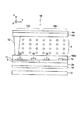
次に、シリンドリカルレンズの焦点距離f及び曲率半径rを算出する。図32は、本実施形態において、レンチキュラレンズを構成するシリンドリカルレンズの焦点距離を算出するための断面図である。なお、図は判別を容易にするために、一部の縮尺を変更して模式的に示している。
(数10)
L:f=w+S:H−f
数式10を整理して、数式11を得ることができる。
(数11)
f=H×L/(L+w+S)
f≦H×L/(L+w+S)
ここで、数式12は、焦点距離fの上限を決定するに過ぎない。そして、焦点距離fを小さくするに従い、レンズの分離性能は低下する。本実施形態において左右画素の分離が損なわれないためには、図33に示すように、レンズピッチLを底辺とし焦点距離fを高さとする三角形と、画素ピッチPを底辺としH−fを高さとする三角形とにおいて、相似の関係を成立させればよい。したがって、下記数式13が成立する。
(数13)
L:f=P:H−f
(数14)
H×L/(L+P)≦f
(数15)
H×L/(L+P)≦f≦H×L/(L+w+S)
更に、レンズの曲率半径rは下記数式16により求めることができる。
(数16)
r=f×(n−1)/n
(数17)
L:f=w+S:f−H
(数18)
H×L/(L−w−S)≦f
(数19)
L:f=P:f−H
(数20)
f≦H×L/(L−P)
数式19と数式20より、焦点距離fを距離Hよりも大きく設定した場合の好ましい焦点距離fの範囲は、下記数式21により求まる。
(数21)
H×L/(L−w−S)≦f≦H×L/(L−P)
即ち、焦点距離fは数式15又は21の何れか一方を満たすことが望ましいと言える。本第16実施形態における上記以外の動作及び効果は、前述の第15実施形態と同様である。
なお、上述の各実施形態は夫々単独で実施してもよいが、適宜組み合わせて実施することも可能である。
1a,11a,12a,13a,14a,15a,16a,17a、18a、19a、20a、21a、22a、23a、24a 反射表示領域
1b,11b,12b,13b,14b,15b,16b,17b、18b、19b、20b、21b、22b、22b1、22b2、23b、24b 透過表示領域
2a 観察者側基板
2b 背面側基板
3a、31a 画素電極
3b、31b 共通電極
3c 縦電界用画素電極
3d 縦電界用共通電極
4a 観察者側円偏光板
4b 背面側円偏光板
5,51 液晶層
6a,61a,62a,63a,64a,65a 観察者側補償板
66a 観察者側補償層
6b,61b,62b,63b,64b,66b 背面側補償板
66b、67b 背面側補償層
68 ポリマーネットワーク型補償層
7 反射板
71 絶縁層
72 柱状スペーサ
73 固着性粒状スペーサ
8 バックライト
9 携帯端末装置
203;レンチキュラレンズ
203a;シリンドリカルレンズ
204L;左眼用画素
204R;右眼用画素
251;右眼
252;左眼
1005 反射領域
1006 透過領域
1007 横電界駆動電極
1008a 第1の絶縁膜
1008b 第2の絶縁膜
1008c 第3の絶縁膜
1009 反射板
1011 下部側基板
1012 対向側基板
1013 液晶層
1021a 偏光板(下部側)
1021b 偏光板(対向側)
1022a 透明絶縁性基板(下部側)
1022b 透明絶縁性基板(対向側)
1026 共通電極
1027 画素電極
1028 バックライト
1029 二分の一波長板
1053 半透過型液晶表示装置
2010 液晶層
2011 第一の基板
2012 第二の基板
2013 第一の配向膜
2014 第二の配向膜
2015 第一の絶縁膜
2016 第二の絶縁膜
2017 第三の絶縁膜
2018 カラーフィルタ
2019 平坦化膜
2021 画素電極
2022 共通電極
2023 ソース配線
2025 信号配線
2051 第一の偏光板
2052 第二の偏光板
2053 第一の位相差板
2054 第二の位相差板
2055 第三の位相差板
2056 光拡散層
3001 上側偏光板
3002 上側2分の1波長板
3003 上側基板
3004 液晶層
3005 透明電極
3006 絶縁層
3007 反射電極
3008 下側基板
3009 下側2分の1波長板
3010 下側偏光板
4001 上側偏光板
4002 上側4分の1波長板
4003 液晶層
4004 反射板
4005 下側4分の1波長板
4006 下側偏光板
4007 バックライト
5001 2分の1波長フィルム
5002 4分の1波長フィルム
5003 直線偏光
5004 円偏光
Claims (30)
- 背面側基板及び観察者側基板とこの両基板に狭持された液晶層とからなり、画素領域に観察者側からの光を反射する反射表示領域と背面側からの光を透過する透過表示領域とを構成し、少なくとも前記透過表示領域の液晶層が、基板面に平行な電圧の印加により横電界駆動される液晶パネルにおいて、
前記液晶層は平行配向されており、前記液晶層が表示面内に屈折率異方性を有し、
前記背面側基板及び観察者側基板それぞれの外側に一枚ずつ設置された円偏光板と、
前記背面側基板の円偏光板と前記背面側基板との間及び前記観察者側基板の円偏光板と前記観察者側基板との間のいずれか一方に前記液晶層の屈折率異方性を低減する機能を有する補償板とを有し、
前記補償板は位相差フィルムからなり、前記位相差フィルム面内にある二つの光学軸をA軸及びB軸と定義したとき、A軸若しくはB軸のうち屈折率の小さい方の軸が電圧非印加時における前記液晶層の屈折率異方性が極大となる方向に配置されることを特徴とする液晶パネル。 - 前記補償板が、前記背面側基板の円偏光板と前記背面側基板との間及び前記観察者側基板の円偏光板と前記観察者側基板との間にそれぞれ1枚ずつ配置され、この2枚の補償板が前記透過表示領域における液晶層の屈折率異方性を低減するように機能し、2枚の補償板のうち一方の補償板が前記反射表示領域における液晶層の屈折率異方性を低減するように機能することを特徴とする請求項1に記載の液晶パネル。
- 前記液晶層の厚みが前記反射表示領域と前記透過表示領域とで異なることを特徴とする請求項2に記載の液晶パネル。
- 前記透過表示領域の液晶層の厚みが、前記反射表示領域の液晶層の厚みの2倍であることを特徴とする請求項2又は3に記載の液晶パネル。
- 前記2枚の補償板が同じ特性を有する補償板であることを特徴とする請求項2乃至4のいずれか一項に記載の液晶パネル。
- 前記2枚の補償板が異なる特性の補償板であることを特徴とする請求項2乃至4のいずれか一項に記載の液晶パネル。
- 前記補償板が、前記各基板と前記円偏光板との間の一方にのみ配置され、この1枚の補償板が前記反射表示領域における液晶層の屈折率異方性と、前記透過表示領域における液晶層の屈折率異方性とを低減するように機能することを特徴とする請求項1に記載の液晶パネル。
- 前記補償板が、前記透過表示領域における液晶層の屈折率異方性を打ち消して等方化する値に設定されていることを特徴とする請求項7に記載の液晶パネル。
- 前記液晶層の厚みが、前記反射表示領域と前記透過表示領域とで等しいことを特徴とする請求項7又は8に記載の液晶パネル。
- 前記液晶層を駆動する電界の強度が、前記反射表示領域と前記透過表示領域で異なることを特徴とする請求項7乃至9のいずれか一項に記載の液晶パネル。
- 前記液晶層を駆動する電界の強度が、前記反射表示領域の方が前記透過表示領域よりも弱いことを特徴とする請求項7乃至10のいずれか一項に記載の液晶パネル。
- 前記反射表示領域における液晶層と電界を発生する電極との間に絶縁層が設けられていることを特徴とする請求項7乃至11のいずれか一項に記載の液晶パネル。
- 前記反射表示領域において横電界を発生する電極の間隔が、前記透過表示領域において横電界を発生する電極の間隔よりも大きいことを特徴とする請求項7乃至12のいずれか一項に記載の液晶パネル。
- 前記補償板が、ネガティブAプレート,ポジティブAプレート,二軸性位相差フィルムの少なくともいずれかの位相差フィルムを用いたものであることを特徴とする請求項1乃至13のいずれか一項に記載の液晶パネル。
- 前記液晶層は平行配向されており、前記補償板は、ネガティブAプレートの位相差フィルムを用いたものであり、このネガティブAプレートの屈折率異常方向が電圧非印加時における前記液晶層の屈折率異方性が極大となる方向に配置されたことを特徴とする請求項1乃至13のいずれか一項に記載の液晶パネル。
- 前記液晶層は平行配向されており、前記補償板は、ポジティブAプレートの位相差フィルムを用いたものであり、このポジティブAプレートの屈折率異常方向が電圧非印加時における前記液晶層の屈折率異方性が極小となる方向に配置されることを特徴とする請求項1乃至13のいずれか一項に記載の液晶パネル。
- 前記液晶層は平行配向されており、前記補償板は、二軸性位相差フィルムを用いたものであり、この二軸性位相差フィルムのA軸若しくはB軸のうち屈折率異方性の小さい方の軸が電圧非印加時における前記液晶層の屈折率異方性が極大となる方向に配置されることを特徴とする請求項1乃至13のいずれか一項に記載の液晶パネル。
- 請求項1乃至17のいずれか一項に記載の液晶パネルを表示部として備えたことを特徴とする液晶表示装置。
- 請求項18に記載の液晶表示装置を備えたことを特徴とする端末装置。
- 携帯電話、個人用情報端末、ゲーム機、デジタルカメラ、ビデオカメラ、ビデオプレーヤ、ノート型パーソナルコンピュータ、キャッシュディスペンサ又は自動販売機であることを特徴とする請求項19に記載の端末装置。
- 背面側基板及び観察者側基板と、前記両基板に狭持された液晶層とからなり、画素領域に観察者側からの光を反射する反射表示領域と背面側からの光を透過する透過表示領域とを構成し、少なくとも前記透過表示領域の液晶層が、基板面に平行な電圧の印加により横電界駆動される液晶パネルにおいて、
前記液晶層は平行配向されており、前記液晶層が表示面内に屈折率異方性を有し、
前記背面側基板及び観察者側基板それぞれの外側に一枚ずつ設置された円偏光板と、
前記背面側基板の円偏光板と前記液晶層との間及び前記観察者側基板の円偏光板と前記液晶層との間の少なくともいずれか一方に前記液晶層の屈折率異方性を低減する機能を有する補償手段とを有し、
前記補償手段は補償層であり、前記補償層は面内にある二つの光学軸をA軸及びB軸と定義したとき、A軸若しくはB軸のうち屈折率の小さい方の軸が電圧非印加時における前記液晶層の屈折率異方性が極大となる方向に配置されることを特徴とする液晶パネル。 - 前記補償手段はポリマーネットワーク補償層であることを特徴とする請求項21に記載の液晶パネル。
- 横電界を発生するための電極は平行電極対であり、この電極幅は前記液晶層の厚さより小さく、前記平行電極対で発生する電界により前記電極間の液晶分子が配向変化し、この配向変化に追従して電極上の液晶分子が前記電極間の液晶分子と同様に配向変化し、この電極上の液晶分子のダイレクタ方向が電極上の電界と異なる方向であることを特徴とする請求項21に記載の液晶パネル。
- 前記平行電極対は金属から構成されることを特徴とする請求項23に記載の液晶パネル。
- 前記平行電極対を構成する電極の幅と間隔との合計値が、前記液晶層の厚さ以下であることを特徴とする請求項23又は24に記載の液晶パネル。
- 前記画素を光学的に拡大する画素拡大手段を有することを特徴とする請求項21に記載の液晶パネル。
- 前記画素拡大手段はレンズであり、少なくとも前記平行電極対の電極配列方向において前記画素を拡大し、前記レンズピッチをL、前記レンズと前記画素との間の距離をH、前記平行電極対の電極幅をw、電極間距離をS、前記画素のピッチをPとするとき、前記レンズの焦点距離fが下記数式の何れか一方を満たすことを特徴とする請求項26に記載の液晶パネル。
H×L/(L+P)≦f≦H×L/(L+w+S)
H×L/(L−w−S)≦f≦H×L/(L−P) - 請求項21乃至27のいずれか一項に記載の液晶パネルを表示部として備えたことを特徴とする液晶表示装置。
- 請求項28に記載の液晶表示装置を備えたことを特徴とする端末装置。
- 携帯電話、個人用情報端末、ゲーム機、デジタルカメラ、ビデオカメラ、ビデオプレーヤ、ノート型パーソナルコンピュータ、キャッシュディスペンサ又は自動販売機であることを特徴とする請求項29に記載の端末装置。
Priority Applications (5)
| Application Number | Priority Date | Filing Date | Title |
|---|---|---|---|
| JP2007070279A JP5278720B2 (ja) | 2006-03-27 | 2007-03-19 | 液晶パネル、液晶表示装置及び端末装置 |
| US11/690,057 US8134663B2 (en) | 2006-03-27 | 2007-03-22 | Liquid crystal panel, liquid crystal display device and terminal device |
| CN2007100897214A CN101046573B (zh) | 2006-03-27 | 2007-03-27 | 液晶面板、液晶显示设备和终端设备 |
| US11/860,875 US8054422B2 (en) | 2006-03-27 | 2007-09-25 | Liquid crystal display device |
| US13/243,562 US8395731B2 (en) | 2006-03-27 | 2011-09-23 | Liquid crystal panel, liquid crystal display device and terminal device |
Applications Claiming Priority (3)
| Application Number | Priority Date | Filing Date | Title |
|---|---|---|---|
| JP2006086629 | 2006-03-27 | ||
| JP2006086629 | 2006-03-27 | ||
| JP2007070279A JP5278720B2 (ja) | 2006-03-27 | 2007-03-19 | 液晶パネル、液晶表示装置及び端末装置 |
Publications (2)
| Publication Number | Publication Date |
|---|---|
| JP2007293290A JP2007293290A (ja) | 2007-11-08 |
| JP5278720B2 true JP5278720B2 (ja) | 2013-09-04 |
Family
ID=38532990
Family Applications (1)
| Application Number | Title | Priority Date | Filing Date |
|---|---|---|---|
| JP2007070279A Expired - Fee Related JP5278720B2 (ja) | 2006-03-27 | 2007-03-19 | 液晶パネル、液晶表示装置及び端末装置 |
Country Status (3)
| Country | Link |
|---|---|
| US (3) | US8134663B2 (ja) |
| JP (1) | JP5278720B2 (ja) |
| CN (1) | CN101046573B (ja) |
Cited By (1)
| Publication number | Priority date | Publication date | Assignee | Title |
|---|---|---|---|---|
| US9971193B2 (en) | 2014-09-05 | 2018-05-15 | Sharp Kabushiki Kaisha | Liquid crystal display panel |
Families Citing this family (52)
| Publication number | Priority date | Publication date | Assignee | Title |
|---|---|---|---|---|
| US9834516B2 (en) * | 2007-02-14 | 2017-12-05 | Eastman Chemical Company | Regioselectively substituted cellulose esters produced in a carboxylated ionic liquid process and products produced therefrom |
| US10174129B2 (en) | 2007-02-14 | 2019-01-08 | Eastman Chemical Company | Regioselectively substituted cellulose esters produced in a carboxylated ionic liquid process and products produced therefrom |
| JP5013370B2 (ja) * | 2007-05-18 | 2012-08-29 | Nltテクノロジー株式会社 | 液晶表示装置及び端末装置 |
| EP2078979A1 (en) * | 2007-12-25 | 2009-07-15 | TPO Displays Corp. | Pixel design having reduced parasitic capacitance for an active matrix display |
| JP2009169353A (ja) * | 2008-01-21 | 2009-07-30 | Hitachi Displays Ltd | 液晶表示装置 |
| US8354525B2 (en) | 2008-02-13 | 2013-01-15 | Eastman Chemical Company | Regioselectively substituted cellulose esters produced in a halogenated ionic liquid process and products produced therefrom |
| US8188267B2 (en) | 2008-02-13 | 2012-05-29 | Eastman Chemical Company | Treatment of cellulose esters |
| US9777074B2 (en) | 2008-02-13 | 2017-10-03 | Eastman Chemical Company | Regioselectively substituted cellulose esters produced in a halogenated ionic liquid process and products produced therefrom |
| JP4613973B2 (ja) * | 2008-03-26 | 2011-01-19 | カシオ計算機株式会社 | 液晶表示素子 |
| JP5159403B2 (ja) * | 2008-04-14 | 2013-03-06 | 三菱電機株式会社 | 液晶表示装置 |
| US20100110351A1 (en) * | 2008-11-03 | 2010-05-06 | Hyang-Yul Kim | Transflective liquid crystal displays |
| US8345177B2 (en) * | 2009-02-13 | 2013-01-01 | Shih Chang Chang | Via design for use in displays |
| US8633879B2 (en) | 2009-02-13 | 2014-01-21 | Apple Inc. | Undulating electrodes for improved viewing angle and color shift |
| US9612489B2 (en) * | 2009-02-13 | 2017-04-04 | Apple Inc. | Placement and shape of electrodes for use in displays |
| US8531408B2 (en) * | 2009-02-13 | 2013-09-10 | Apple Inc. | Pseudo multi-domain design for improved viewing angle and color shift |
| US8558978B2 (en) * | 2009-02-13 | 2013-10-15 | Apple Inc. | LCD panel with index-matching passivation layers |
| US20100208179A1 (en) * | 2009-02-13 | 2010-08-19 | Apple Inc. | Pixel Black Mask Design and Formation Technique |
| US8390553B2 (en) * | 2009-02-13 | 2013-03-05 | Apple Inc. | Advanced pixel design for optimized driving |
| US8587758B2 (en) * | 2009-02-13 | 2013-11-19 | Apple Inc. | Electrodes for use in displays |
| US8294647B2 (en) * | 2009-02-13 | 2012-10-23 | Apple Inc. | LCD pixel design varying by color |
| JP4375497B1 (ja) | 2009-03-11 | 2009-12-02 | 住友電気工業株式会社 | Iii族窒化物半導体素子、エピタキシャル基板、及びiii族窒化物半導体素子を作製する方法 |
| US8111232B2 (en) * | 2009-03-27 | 2012-02-07 | Apple Inc. | LCD electrode arrangement |
| US8294850B2 (en) * | 2009-03-31 | 2012-10-23 | Apple Inc. | LCD panel having improved response |
| US8524887B2 (en) * | 2009-04-15 | 2013-09-03 | Eastman Chemical Company | Regioselectively substituted cellulose esters produced in a tetraalkylammonium alkylphosphate ionic liquid process and products produced therefrom |
| JP2011075630A (ja) * | 2009-09-29 | 2011-04-14 | Canon Inc | 画像表示装置 |
| JP2011075745A (ja) * | 2009-09-30 | 2011-04-14 | Sony Corp | 画像表示観察システム、光変調器、及び画像表示装置 |
| KR101236244B1 (ko) * | 2009-12-11 | 2013-02-22 | 엘지디스플레이 주식회사 | 액정표시장치 |
| CN102253495B (zh) * | 2010-05-18 | 2013-10-30 | 京东方科技集团股份有限公司 | 双视显示设备和系统 |
| US20120007856A1 (en) * | 2010-07-07 | 2012-01-12 | Edzer Lienson Wu | Stereoscopic display device |
| CN102466918A (zh) * | 2010-11-16 | 2012-05-23 | 吴亿泽 | 立体显示装置及其显示方法 |
| WO2012090839A1 (ja) * | 2010-12-28 | 2012-07-05 | シャープ株式会社 | 液晶パネル、及び、液晶ディスプレイ |
| US9096691B2 (en) | 2011-04-13 | 2015-08-04 | Eastman Chemical Company | Cellulose ester optical films |
| US9315811B2 (en) | 2011-06-10 | 2016-04-19 | Ionis Pharmaceuticals, Inc. | Methods for modulating kallikrein (KLKB1) expression |
| KR101910599B1 (ko) * | 2011-06-24 | 2018-10-23 | 삼성전자주식회사 | 광학 보상 필름 및 이를 포함하는 액정 표시 장치 |
| CN202886791U (zh) * | 2012-08-31 | 2013-04-17 | 京东方科技集团股份有限公司 | 视角补偿装置、垂直取向液晶显示面板和液晶显示装置 |
| CN102854659B (zh) * | 2012-09-24 | 2015-01-07 | 深圳市华星光电技术有限公司 | 一种使用光学补偿膜减弱va液晶显示器暗态漏光的方法 |
| US9176347B2 (en) * | 2012-12-07 | 2015-11-03 | Vastview Technology Inc. | Lateral electric field type liquid crystal display device having non-uniform spacings between two electrodes |
| TW201423236A (zh) * | 2012-12-11 | 2014-06-16 | Wintek Corp | 可切換二維顯示模式與三維顯示模式之顯示裝置及其液晶透鏡 |
| TWI493265B (zh) * | 2012-12-20 | 2015-07-21 | Vastview Tech Inc | 橫向電場型液晶顯示器 |
| JP2014157315A (ja) * | 2013-02-18 | 2014-08-28 | Japan Display Inc | 液晶表示装置 |
| US9575363B2 (en) | 2013-08-08 | 2017-02-21 | Tokyo University Of Science Foundation | Method for improving optical response and liquid crystal display device using same |
| WO2015103709A1 (en) * | 2014-01-11 | 2015-07-16 | UNIVERSITé LAVAL | Method and apparatus for creation and electrical tuning of spatially non-uniform reflection of light |
| CN105068299B (zh) * | 2015-07-27 | 2018-06-15 | 武汉华星光电技术有限公司 | 一种显示面板及液晶显示器 |
| US10782556B2 (en) * | 2015-07-29 | 2020-09-22 | Sharp Kabushiki Kaisha | Sunlight readable LCD with uniform in-cell retarder |
| US10591767B2 (en) * | 2015-07-29 | 2020-03-17 | Sharp Kabushiki Kaisha | Sunlight readable LCD with uniform in-cell retarder |
| KR20170040863A (ko) * | 2015-10-05 | 2017-04-14 | 삼성디스플레이 주식회사 | 투광성 도전막 및 이를 포함하는 액정 표시 장치 |
| CN105223725A (zh) * | 2015-10-13 | 2016-01-06 | 京东方科技集团股份有限公司 | 显示面板及其制备方法 |
| TWI567464B (zh) | 2015-12-01 | 2017-01-21 | 友達光電股份有限公司 | 液晶顯示面板 |
| CN105629558A (zh) * | 2016-01-11 | 2016-06-01 | 武汉华星光电技术有限公司 | 一种具有反射区的液晶显示装置 |
| CN109188755B (zh) * | 2018-10-29 | 2021-11-26 | 上海天马微电子有限公司 | 显示面板和显示装置 |
| CN113449575B (zh) * | 2020-08-06 | 2022-08-05 | 重庆康佳光电技术研究院有限公司 | 一种显示背板、显示面板、显示背板的制作方法及终端 |
| US20220155636A1 (en) * | 2020-11-18 | 2022-05-19 | Sharp Kabushiki Kaisha | Liquid crystal display device |
Family Cites Families (37)
| Publication number | Priority date | Publication date | Assignee | Title |
|---|---|---|---|---|
| EP0470817A3 (en) * | 1990-08-09 | 1992-11-25 | Seiko Epson Corporation | Liquid crystal electro-optical device |
| JP3380482B2 (ja) * | 1997-12-26 | 2003-02-24 | シャープ株式会社 | 液晶表示装置 |
| JP3822361B2 (ja) * | 1998-07-10 | 2006-09-20 | 株式会社日立製作所 | 配光制御素子およびこれを備えた表示装置 |
| US6693689B1 (en) * | 1999-03-31 | 2004-02-17 | Lg Philips Lcd Co., Ltd. | Reflective liquid crystal display device |
| KR100294822B1 (ko) * | 1999-06-05 | 2001-07-12 | 구본준, 론 위라하디락사 | 반사형 액정표시소자. |
| US6822711B1 (en) * | 1999-09-30 | 2004-11-23 | Casio Computer Co., Ltd. | Liquid crystal display apparatus using polarizing element transmitting one of two polarizing components crossing at right angles and reflecting the other component |
| KR100394987B1 (ko) * | 2000-04-07 | 2003-08-19 | 엘지.필립스 엘시디 주식회사 | 반투과 액정 표시장치 |
| JP3949924B2 (ja) * | 2001-10-15 | 2007-07-25 | シャープ株式会社 | 反射型液晶表示装置用基板およびそれを用いた反射型液晶表示装置 |
| JP4002105B2 (ja) * | 2002-01-15 | 2007-10-31 | 株式会社日立製作所 | 液晶表示装置 |
| JP3788421B2 (ja) * | 2002-04-02 | 2006-06-21 | セイコーエプソン株式会社 | 液晶表示装置およびその製造方法ならびに電子機器 |
| US6650385B1 (en) * | 2002-04-24 | 2003-11-18 | Prime View International Co., Ltd. | Scattering fringe field optical-compensated reflective and transflective liquid crystal display |
| JP4117148B2 (ja) * | 2002-05-24 | 2008-07-16 | 日本電気株式会社 | 半透過型液晶表示装置 |
| US7719646B2 (en) * | 2002-11-15 | 2010-05-18 | Sharp Kabushiki Kaisha | Liquid crystal display device |
| JP2004302359A (ja) * | 2003-04-01 | 2004-10-28 | Casio Comput Co Ltd | 液晶表示装置 |
| US7164456B2 (en) * | 2003-04-08 | 2007-01-16 | Lg.Philips Lcd Co., Ltd | Liquid crystal display device and method of fabricating the same wherein having particular reflective electrode |
| JP2004341207A (ja) * | 2003-05-15 | 2004-12-02 | Koninkl Philips Electronics Nv | 液晶表示装置 |
| US7924384B2 (en) * | 2003-07-14 | 2011-04-12 | Hitachi Displays, Ltd. | Display device |
| JP4082683B2 (ja) * | 2003-09-29 | 2008-04-30 | 株式会社 日立ディスプレイズ | 半透過型液晶表示装置 |
| CN100543522C (zh) * | 2003-12-12 | 2009-09-23 | 鸿富锦精密工业(深圳)有限公司 | 边缘电场开关型液晶显示装置 |
| CN100376932C (zh) * | 2003-12-12 | 2008-03-26 | 鸿富锦精密工业(深圳)有限公司 | 液晶显示装置 |
| CN1629682A (zh) * | 2003-12-19 | 2005-06-22 | 鸿富锦精密工业(深圳)有限公司 | 边缘电场开关型液晶显示装置 |
| TWI281567B (en) * | 2003-12-31 | 2007-05-21 | Innolux Display Corp | Liquid crystal display device |
| TWI321697B (en) * | 2004-02-13 | 2010-03-11 | Innolux Display Corp | Liquid crystal display device |
| JP2005266778A (ja) * | 2004-02-19 | 2005-09-29 | Sharp Corp | 液晶表示装置 |
| JP2005265953A (ja) * | 2004-03-16 | 2005-09-29 | Chisso Corp | 液晶表示素子 |
| JP2005292225A (ja) * | 2004-03-31 | 2005-10-20 | Nitto Denko Corp | 光学フィルムおよび画像表示装置 |
| JP2005292709A (ja) * | 2004-04-05 | 2005-10-20 | Toshiba Matsushita Display Technology Co Ltd | 液晶表示素子 |
| TWI278709B (en) * | 2004-04-30 | 2007-04-11 | Innolux Display Corp | Liquid crystal display device |
| TW200537174A (en) * | 2004-05-14 | 2005-11-16 | Innolux Display Corp | A transflecitive liquid crystal display apparatus |
| CN100483226C (zh) * | 2004-05-28 | 2009-04-29 | 鸿富锦精密工业(深圳)有限公司 | 半穿透式液晶显示装置 |
| JP2006126551A (ja) * | 2004-10-29 | 2006-05-18 | Hitachi Displays Ltd | 液晶表示装置 |
| JP4816862B2 (ja) * | 2004-12-16 | 2011-11-16 | ソニー株式会社 | 液晶表示装置 |
| TWI283483B (en) * | 2005-02-01 | 2007-07-01 | Innolux Display Corp | TFT LCD and fabricating method thereof |
| JP4138759B2 (ja) * | 2005-02-03 | 2008-08-27 | セイコーエプソン株式会社 | 液晶表示装置および電子機器 |
| JP2006251050A (ja) * | 2005-03-08 | 2006-09-21 | Toshiba Matsushita Display Technology Co Ltd | 液晶表示素子 |
| KR100648223B1 (ko) * | 2005-05-11 | 2006-11-24 | 비오이 하이디스 테크놀로지 주식회사 | 반투과형 프린지 필드 스위칭 모드 액정표시장치 |
| CN102331639A (zh) * | 2005-12-05 | 2012-01-25 | 株式会社半导体能源研究所 | 液晶显示器 |
-
2007
- 2007-03-19 JP JP2007070279A patent/JP5278720B2/ja not_active Expired - Fee Related
- 2007-03-22 US US11/690,057 patent/US8134663B2/en not_active Expired - Fee Related
- 2007-03-27 CN CN2007100897214A patent/CN101046573B/zh active Active
- 2007-09-25 US US11/860,875 patent/US8054422B2/en not_active Expired - Fee Related
-
2011
- 2011-09-23 US US13/243,562 patent/US8395731B2/en active Active
Cited By (1)
| Publication number | Priority date | Publication date | Assignee | Title |
|---|---|---|---|---|
| US9971193B2 (en) | 2014-09-05 | 2018-05-15 | Sharp Kabushiki Kaisha | Liquid crystal display panel |
Also Published As
| Publication number | Publication date |
|---|---|
| US8054422B2 (en) | 2011-11-08 |
| US8395731B2 (en) | 2013-03-12 |
| US8134663B2 (en) | 2012-03-13 |
| US20070222927A1 (en) | 2007-09-27 |
| CN101046573B (zh) | 2010-07-21 |
| CN101046573A (zh) | 2007-10-03 |
| JP2007293290A (ja) | 2007-11-08 |
| US20080018840A1 (en) | 2008-01-24 |
| US20120075554A1 (en) | 2012-03-29 |
Similar Documents
| Publication | Publication Date | Title |
|---|---|---|
| JP5278720B2 (ja) | 液晶パネル、液晶表示装置及び端末装置 | |
| JP5131510B2 (ja) | 液晶表示装置、及び端末装置 | |
| US7400367B2 (en) | Viewing angle control element, display device, and electronic apparatus | |
| US7852445B2 (en) | Liquid crystal display device and terminal device that uses same | |
| TWI410721B (zh) | 水平驅動型液晶顯示裝置 | |
| JP2008310271A (ja) | 液晶表示装置及び視野角制御パネル | |
| JP4822535B2 (ja) | 液晶表示装置及びそれを用いた端末装置 | |
| JP5252335B2 (ja) | 液晶表示装置、および端末装置 | |
| JP4899153B2 (ja) | 液晶表示装置 | |
| JP3901074B2 (ja) | 液晶表示装置及び電子機器 | |
| JP5239973B2 (ja) | 液晶表示装置 | |
| JP2003322855A (ja) | 液晶表示素子 | |
| JP2006126551A (ja) | 液晶表示装置 | |
| JP2005107501A (ja) | 液晶表示装置 | |
| JP4390595B2 (ja) | 液晶表示装置 | |
| WO2010016284A1 (ja) | 垂直配向型液晶表示装置 | |
| JP2892913B2 (ja) | 反射型液晶表示装置 | |
| JP3807503B2 (ja) | 液晶表示装置および電子機器 | |
| JP4337843B2 (ja) | 液晶表示装置及び電子機器 | |
| JP4619742B2 (ja) | 液晶表示装置 | |
| JP2009003432A (ja) | 液晶表示装置 | |
| JP4824443B2 (ja) | 液晶表示装置 | |
| Sytsma | ADVANCEMENTS IN LUMINANCE VIEW ANGLE DISTRIBUTIONS IN LIQUID CRYSTAL DISPLAYS | |
| JP4607237B2 (ja) | 液晶表示装置及びその製造方法 | |
| JP4609382B2 (ja) | 液晶表示装置及び電子機器 |
Legal Events
| Date | Code | Title | Description |
|---|---|---|---|
| A621 | Written request for application examination |
Free format text: JAPANESE INTERMEDIATE CODE: A621 Effective date: 20090612 |
|
| A521 | Request for written amendment filed |
Free format text: JAPANESE INTERMEDIATE CODE: A523 Effective date: 20090729 |
|
| A711 | Notification of change in applicant |
Free format text: JAPANESE INTERMEDIATE CODE: A711 Effective date: 20100315 |
|
| A977 | Report on retrieval |
Free format text: JAPANESE INTERMEDIATE CODE: A971007 Effective date: 20111102 |
|
| A131 | Notification of reasons for refusal |
Free format text: JAPANESE INTERMEDIATE CODE: A131 Effective date: 20111206 |
|
| A521 | Request for written amendment filed |
Free format text: JAPANESE INTERMEDIATE CODE: A523 Effective date: 20120116 |
|
| A131 | Notification of reasons for refusal |
Free format text: JAPANESE INTERMEDIATE CODE: A131 Effective date: 20120724 |
|
| A521 | Request for written amendment filed |
Free format text: JAPANESE INTERMEDIATE CODE: A523 Effective date: 20120914 |
|
| TRDD | Decision of grant or rejection written | ||
| A01 | Written decision to grant a patent or to grant a registration (utility model) |
Free format text: JAPANESE INTERMEDIATE CODE: A01 Effective date: 20130423 |
|
| A61 | First payment of annual fees (during grant procedure) |
Free format text: JAPANESE INTERMEDIATE CODE: A61 Effective date: 20130508 |
|
| R150 | Certificate of patent or registration of utility model |
Free format text: JAPANESE INTERMEDIATE CODE: R150 Ref document number: 5278720 Country of ref document: JP Free format text: JAPANESE INTERMEDIATE CODE: R150 |
|
| R250 | Receipt of annual fees |
Free format text: JAPANESE INTERMEDIATE CODE: R250 |
|
| R250 | Receipt of annual fees |
Free format text: JAPANESE INTERMEDIATE CODE: R250 |
|
| R250 | Receipt of annual fees |
Free format text: JAPANESE INTERMEDIATE CODE: R250 |
|
| R250 | Receipt of annual fees |
Free format text: JAPANESE INTERMEDIATE CODE: R250 |
|
| R250 | Receipt of annual fees |
Free format text: JAPANESE INTERMEDIATE CODE: R250 |
|
| R250 | Receipt of annual fees |
Free format text: JAPANESE INTERMEDIATE CODE: R250 |
|
| LAPS | Cancellation because of no payment of annual fees |