JP5247438B2 - ナノ構造物の製造方法 - Google Patents
ナノ構造物の製造方法 Download PDFInfo
- Publication number
- JP5247438B2 JP5247438B2 JP2008514165A JP2008514165A JP5247438B2 JP 5247438 B2 JP5247438 B2 JP 5247438B2 JP 2008514165 A JP2008514165 A JP 2008514165A JP 2008514165 A JP2008514165 A JP 2008514165A JP 5247438 B2 JP5247438 B2 JP 5247438B2
- Authority
- JP
- Japan
- Prior art keywords
- layer
- catalyst
- cathode
- nanostructure
- nanostructures
- Prior art date
- Legal status (The legal status is an assumption and is not a legal conclusion. Google has not performed a legal analysis and makes no representation as to the accuracy of the status listed.)
- Active
Links
- 239000002086 nanomaterial Substances 0.000 title claims description 147
- 238000004519 manufacturing process Methods 0.000 title claims description 41
- 239000010410 layer Substances 0.000 claims description 309
- 239000003054 catalyst Substances 0.000 claims description 150
- 239000002344 surface layer Substances 0.000 claims description 69
- 238000005530 etching Methods 0.000 claims description 59
- 230000004888 barrier function Effects 0.000 claims description 53
- 239000000463 material Substances 0.000 claims description 50
- 230000012010 growth Effects 0.000 claims description 39
- 238000000034 method Methods 0.000 claims description 30
- 238000000605 extraction Methods 0.000 claims description 18
- 229910052751 metal Inorganic materials 0.000 claims description 18
- 239000002184 metal Substances 0.000 claims description 18
- 239000004020 conductor Substances 0.000 claims description 13
- 238000013467 fragmentation Methods 0.000 claims description 12
- 238000006062 fragmentation reaction Methods 0.000 claims description 12
- 239000012777 electrically insulating material Substances 0.000 claims description 11
- 238000009792 diffusion process Methods 0.000 claims description 8
- 238000005229 chemical vapour deposition Methods 0.000 claims description 7
- 238000000137 annealing Methods 0.000 claims description 5
- 230000000694 effects Effects 0.000 claims description 3
- 239000011810 insulating material Substances 0.000 claims 1
- 239000002071 nanotube Substances 0.000 description 21
- PXHVJJICTQNCMI-UHFFFAOYSA-N nickel Substances [Ni] PXHVJJICTQNCMI-UHFFFAOYSA-N 0.000 description 16
- OKTJSMMVPCPJKN-UHFFFAOYSA-N Carbon Chemical compound [C] OKTJSMMVPCPJKN-UHFFFAOYSA-N 0.000 description 11
- 239000002041 carbon nanotube Substances 0.000 description 10
- 229910021393 carbon nanotube Inorganic materials 0.000 description 10
- VYPSYNLAJGMNEJ-UHFFFAOYSA-N Silicium dioxide Chemical compound O=[Si]=O VYPSYNLAJGMNEJ-UHFFFAOYSA-N 0.000 description 8
- ATJFFYVFTNAWJD-UHFFFAOYSA-N Tin Chemical compound [Sn] ATJFFYVFTNAWJD-UHFFFAOYSA-N 0.000 description 8
- 229920002120 photoresistant polymer Polymers 0.000 description 8
- 229910052718 tin Inorganic materials 0.000 description 8
- 238000010586 diagram Methods 0.000 description 7
- 239000000758 substrate Substances 0.000 description 7
- QTBSBXVTEAMEQO-UHFFFAOYSA-N Acetic acid Chemical compound CC(O)=O QTBSBXVTEAMEQO-UHFFFAOYSA-N 0.000 description 6
- 239000002717 carbon nanostructure Substances 0.000 description 6
- 238000000151 deposition Methods 0.000 description 6
- 238000009826 distribution Methods 0.000 description 6
- 230000005684 electric field Effects 0.000 description 6
- 239000012528 membrane Substances 0.000 description 6
- 229910052782 aluminium Inorganic materials 0.000 description 5
- XAGFODPZIPBFFR-UHFFFAOYSA-N aluminium Chemical compound [Al] XAGFODPZIPBFFR-UHFFFAOYSA-N 0.000 description 5
- 239000007787 solid Substances 0.000 description 5
- RYGMFSIKBFXOCR-UHFFFAOYSA-N Copper Chemical compound [Cu] RYGMFSIKBFXOCR-UHFFFAOYSA-N 0.000 description 4
- NBIIXXVUZAFLBC-UHFFFAOYSA-N Phosphoric acid Chemical compound OP(O)(O)=O NBIIXXVUZAFLBC-UHFFFAOYSA-N 0.000 description 4
- 229910052802 copper Inorganic materials 0.000 description 4
- 239000010949 copper Substances 0.000 description 4
- 230000008021 deposition Effects 0.000 description 4
- 238000001312 dry etching Methods 0.000 description 4
- 239000002070 nanowire Substances 0.000 description 4
- 238000000206 photolithography Methods 0.000 description 4
- 239000000377 silicon dioxide Substances 0.000 description 4
- 238000001039 wet etching Methods 0.000 description 4
- 229910052804 chromium Inorganic materials 0.000 description 3
- 239000011651 chromium Substances 0.000 description 3
- 229910003460 diamond Inorganic materials 0.000 description 3
- 239000010432 diamond Substances 0.000 description 3
- 239000011521 glass Substances 0.000 description 3
- 229910052750 molybdenum Inorganic materials 0.000 description 3
- 239000002245 particle Substances 0.000 description 3
- 238000001771 vacuum deposition Methods 0.000 description 3
- VYZAMTAEIAYCRO-UHFFFAOYSA-N Chromium Chemical compound [Cr] VYZAMTAEIAYCRO-UHFFFAOYSA-N 0.000 description 2
- UFHFLCQGNIYNRP-UHFFFAOYSA-N Hydrogen Chemical compound [H][H] UFHFLCQGNIYNRP-UHFFFAOYSA-N 0.000 description 2
- GRYLNZFGIOXLOG-UHFFFAOYSA-N Nitric acid Chemical compound O[N+]([O-])=O GRYLNZFGIOXLOG-UHFFFAOYSA-N 0.000 description 2
- 238000005136 cathodoluminescence Methods 0.000 description 2
- 230000001419 dependent effect Effects 0.000 description 2
- 229910052739 hydrogen Inorganic materials 0.000 description 2
- 239000001257 hydrogen Substances 0.000 description 2
- 238000009413 insulation Methods 0.000 description 2
- 229910052742 iron Inorganic materials 0.000 description 2
- 238000002955 isolation Methods 0.000 description 2
- 239000000203 mixture Substances 0.000 description 2
- -1 nanofilaments Substances 0.000 description 2
- 229910017604 nitric acid Inorganic materials 0.000 description 2
- VLTRZXGMWDSKGL-UHFFFAOYSA-N perchloric acid Chemical compound OCl(=O)(=O)=O VLTRZXGMWDSKGL-UHFFFAOYSA-N 0.000 description 2
- 235000011007 phosphoric acid Nutrition 0.000 description 2
- 238000009832 plasma treatment Methods 0.000 description 2
- 239000002243 precursor Substances 0.000 description 2
- 239000011241 protective layer Substances 0.000 description 2
- 239000000126 substance Substances 0.000 description 2
- ZOKXTWBITQBERF-UHFFFAOYSA-N Molybdenum Chemical compound [Mo] ZOKXTWBITQBERF-UHFFFAOYSA-N 0.000 description 1
- 229910052581 Si3N4 Inorganic materials 0.000 description 1
- 229910004166 TaN Inorganic materials 0.000 description 1
- 229910008599 TiW Inorganic materials 0.000 description 1
- 238000005054 agglomeration Methods 0.000 description 1
- 230000002776 aggregation Effects 0.000 description 1
- 239000000956 alloy Substances 0.000 description 1
- 229910045601 alloy Inorganic materials 0.000 description 1
- HSFWRNGVRCDJHI-UHFFFAOYSA-N alpha-acetylene Natural products C#C HSFWRNGVRCDJHI-UHFFFAOYSA-N 0.000 description 1
- 229910021417 amorphous silicon Inorganic materials 0.000 description 1
- HKVFISRIUUGTIB-UHFFFAOYSA-O azanium;cerium;nitrate Chemical compound [NH4+].[Ce].[O-][N+]([O-])=O HKVFISRIUUGTIB-UHFFFAOYSA-O 0.000 description 1
- 230000015572 biosynthetic process Effects 0.000 description 1
- 229910052799 carbon Inorganic materials 0.000 description 1
- 230000015556 catabolic process Effects 0.000 description 1
- 230000003197 catalytic effect Effects 0.000 description 1
- 238000003486 chemical etching Methods 0.000 description 1
- 239000007795 chemical reaction product Substances 0.000 description 1
- 239000002131 composite material Substances 0.000 description 1
- 238000004070 electrodeposition Methods 0.000 description 1
- 125000002534 ethynyl group Chemical group [H]C#C* 0.000 description 1
- 230000005669 field effect Effects 0.000 description 1
- 239000012634 fragment Substances 0.000 description 1
- 238000011065 in-situ storage Methods 0.000 description 1
- 150000002500 ions Chemical class 0.000 description 1
- 238000004020 luminiscence type Methods 0.000 description 1
- 238000001465 metallisation Methods 0.000 description 1
- 150000002739 metals Chemical class 0.000 description 1
- 238000002156 mixing Methods 0.000 description 1
- 239000011733 molybdenum Substances 0.000 description 1
- 239000002105 nanoparticle Substances 0.000 description 1
- 229910052759 nickel Inorganic materials 0.000 description 1
- 229910052758 niobium Inorganic materials 0.000 description 1
- 239000010955 niobium Substances 0.000 description 1
- GUCVJGMIXFAOAE-UHFFFAOYSA-N niobium atom Chemical compound [Nb] GUCVJGMIXFAOAE-UHFFFAOYSA-N 0.000 description 1
- 238000000623 plasma-assisted chemical vapour deposition Methods 0.000 description 1
- 229910052697 platinum Inorganic materials 0.000 description 1
- 239000000047 product Substances 0.000 description 1
- 230000005855 radiation Effects 0.000 description 1
- 239000011347 resin Substances 0.000 description 1
- 229920005989 resin Polymers 0.000 description 1
- 230000002786 root growth Effects 0.000 description 1
- 235000012239 silicon dioxide Nutrition 0.000 description 1
- HQVNEWCFYHHQES-UHFFFAOYSA-N silicon nitride Chemical compound N12[Si]34N5[Si]62N3[Si]51N64 HQVNEWCFYHHQES-UHFFFAOYSA-N 0.000 description 1
- 238000004544 sputter deposition Methods 0.000 description 1
- 238000007740 vapor deposition Methods 0.000 description 1
- 238000001947 vapour-phase growth Methods 0.000 description 1
- XLYOFNOQVPJJNP-UHFFFAOYSA-N water Substances O XLYOFNOQVPJJNP-UHFFFAOYSA-N 0.000 description 1
Images


Classifications
-
- H—ELECTRICITY
- H01—ELECTRIC ELEMENTS
- H01J—ELECTRIC DISCHARGE TUBES OR DISCHARGE LAMPS
- H01J9/00—Apparatus or processes specially adapted for the manufacture, installation, removal, maintenance of electric discharge tubes, discharge lamps, or parts thereof; Recovery of material from discharge tubes or lamps
- H01J9/02—Manufacture of electrodes or electrode systems
- H01J9/022—Manufacture of electrodes or electrode systems of cold cathodes
- H01J9/025—Manufacture of electrodes or electrode systems of cold cathodes of field emission cathodes
-
- B—PERFORMING OPERATIONS; TRANSPORTING
- B82—NANOTECHNOLOGY
- B82Y—SPECIFIC USES OR APPLICATIONS OF NANOSTRUCTURES; MEASUREMENT OR ANALYSIS OF NANOSTRUCTURES; MANUFACTURE OR TREATMENT OF NANOSTRUCTURES
- B82Y10/00—Nanotechnology for information processing, storage or transmission, e.g. quantum computing or single electron logic
-
- B—PERFORMING OPERATIONS; TRANSPORTING
- B82—NANOTECHNOLOGY
- B82Y—SPECIFIC USES OR APPLICATIONS OF NANOSTRUCTURES; MEASUREMENT OR ANALYSIS OF NANOSTRUCTURES; MANUFACTURE OR TREATMENT OF NANOSTRUCTURES
- B82Y30/00—Nanotechnology for materials or surface science, e.g. nanocomposites
-
- B—PERFORMING OPERATIONS; TRANSPORTING
- B82—NANOTECHNOLOGY
- B82Y—SPECIFIC USES OR APPLICATIONS OF NANOSTRUCTURES; MEASUREMENT OR ANALYSIS OF NANOSTRUCTURES; MANUFACTURE OR TREATMENT OF NANOSTRUCTURES
- B82Y40/00—Manufacture or treatment of nanostructures
-
- C—CHEMISTRY; METALLURGY
- C01—INORGANIC CHEMISTRY
- C01B—NON-METALLIC ELEMENTS; COMPOUNDS THEREOF; METALLOIDS OR COMPOUNDS THEREOF NOT COVERED BY SUBCLASS C01C
- C01B32/00—Carbon; Compounds thereof
- C01B32/15—Nano-sized carbon materials
- C01B32/158—Carbon nanotubes
- C01B32/16—Preparation
- C01B32/162—Preparation characterised by catalysts
-
- D—TEXTILES; PAPER
- D01—NATURAL OR MAN-MADE THREADS OR FIBRES; SPINNING
- D01F—CHEMICAL FEATURES IN THE MANUFACTURE OF ARTIFICIAL FILAMENTS, THREADS, FIBRES, BRISTLES OR RIBBONS; APPARATUS SPECIALLY ADAPTED FOR THE MANUFACTURE OF CARBON FILAMENTS
- D01F9/00—Artificial filaments or the like of other substances; Manufacture thereof; Apparatus specially adapted for the manufacture of carbon filaments
- D01F9/08—Artificial filaments or the like of other substances; Manufacture thereof; Apparatus specially adapted for the manufacture of carbon filaments of inorganic material
- D01F9/12—Carbon filaments; Apparatus specially adapted for the manufacture thereof
- D01F9/127—Carbon filaments; Apparatus specially adapted for the manufacture thereof by thermal decomposition of hydrocarbon gases or vapours or other carbon-containing compounds in the form of gas or vapour, e.g. carbon monoxide, alcohols
-
- H—ELECTRICITY
- H01—ELECTRIC ELEMENTS
- H01J—ELECTRIC DISCHARGE TUBES OR DISCHARGE LAMPS
- H01J1/00—Details of electrodes, of magnetic control means, of screens, or of the mounting or spacing thereof, common to two or more basic types of discharge tubes or lamps
- H01J1/02—Main electrodes
- H01J1/30—Cold cathodes, e.g. field-emissive cathode
- H01J1/304—Field-emissive cathodes
- H01J1/3048—Distributed particle emitters
-
- H—ELECTRICITY
- H01—ELECTRIC ELEMENTS
- H01J—ELECTRIC DISCHARGE TUBES OR DISCHARGE LAMPS
- H01J31/00—Cathode ray tubes; Electron beam tubes
- H01J31/08—Cathode ray tubes; Electron beam tubes having a screen on or from which an image or pattern is formed, picked up, converted, or stored
- H01J31/10—Image or pattern display tubes, i.e. having electrical input and optical output; Flying-spot tubes for scanning purposes
- H01J31/12—Image or pattern display tubes, i.e. having electrical input and optical output; Flying-spot tubes for scanning purposes with luminescent screen
- H01J31/123—Flat display tubes
- H01J31/125—Flat display tubes provided with control means permitting the electron beam to reach selected parts of the screen, e.g. digital selection
- H01J31/127—Flat display tubes provided with control means permitting the electron beam to reach selected parts of the screen, e.g. digital selection using large area or array sources, i.e. essentially a source for each pixel group
-
- H—ELECTRICITY
- H10—SEMICONDUCTOR DEVICES; ELECTRIC SOLID-STATE DEVICES NOT OTHERWISE PROVIDED FOR
- H10K—ORGANIC ELECTRIC SOLID-STATE DEVICES
- H10K10/00—Organic devices specially adapted for rectifying, amplifying, oscillating or switching; Organic capacitors or resistors having potential barriers
- H10K10/40—Organic transistors
- H10K10/46—Field-effect transistors, e.g. organic thin-film transistors [OTFT]
- H10K10/462—Insulated gate field-effect transistors [IGFETs]
- H10K10/464—Lateral top-gate IGFETs comprising only a single gate
-
- H—ELECTRICITY
- H10—SEMICONDUCTOR DEVICES; ELECTRIC SOLID-STATE DEVICES NOT OTHERWISE PROVIDED FOR
- H10K—ORGANIC ELECTRIC SOLID-STATE DEVICES
- H10K10/00—Organic devices specially adapted for rectifying, amplifying, oscillating or switching; Organic capacitors or resistors having potential barriers
- H10K10/40—Organic transistors
- H10K10/46—Field-effect transistors, e.g. organic thin-film transistors [OTFT]
- H10K10/462—Insulated gate field-effect transistors [IGFETs]
- H10K10/481—Insulated gate field-effect transistors [IGFETs] characterised by the gate conductors
-
- H—ELECTRICITY
- H01—ELECTRIC ELEMENTS
- H01J—ELECTRIC DISCHARGE TUBES OR DISCHARGE LAMPS
- H01J2201/00—Electrodes common to discharge tubes
- H01J2201/30—Cold cathodes
- H01J2201/304—Field emission cathodes
- H01J2201/30446—Field emission cathodes characterised by the emitter material
- H01J2201/30453—Carbon types
- H01J2201/30469—Carbon nanotubes (CNTs)
-
- H—ELECTRICITY
- H01—ELECTRIC ELEMENTS
- H01J—ELECTRIC DISCHARGE TUBES OR DISCHARGE LAMPS
- H01J2201/00—Electrodes common to discharge tubes
- H01J2201/30—Cold cathodes
- H01J2201/319—Circuit elements associated with the emitters by direct integration
-
- H—ELECTRICITY
- H10—SEMICONDUCTOR DEVICES; ELECTRIC SOLID-STATE DEVICES NOT OTHERWISE PROVIDED FOR
- H10K—ORGANIC ELECTRIC SOLID-STATE DEVICES
- H10K85/00—Organic materials used in the body or electrodes of devices covered by this subclass
- H10K85/20—Carbon compounds, e.g. carbon nanotubes or fullerenes
- H10K85/221—Carbon nanotubes
Landscapes
- Engineering & Computer Science (AREA)
- Chemical & Material Sciences (AREA)
- Nanotechnology (AREA)
- Materials Engineering (AREA)
- Physics & Mathematics (AREA)
- Crystallography & Structural Chemistry (AREA)
- Chemical Kinetics & Catalysis (AREA)
- Organic Chemistry (AREA)
- Manufacturing & Machinery (AREA)
- Condensed Matter Physics & Semiconductors (AREA)
- General Physics & Mathematics (AREA)
- Inorganic Chemistry (AREA)
- Composite Materials (AREA)
- Thermal Sciences (AREA)
- General Chemical & Material Sciences (AREA)
- Textile Engineering (AREA)
- Mathematical Physics (AREA)
- Theoretical Computer Science (AREA)
- Cold Cathode And The Manufacture (AREA)
- Carbon And Carbon Compounds (AREA)
- Cathode-Ray Tubes And Fluorescent Screens For Display (AREA)
- Chemical Vapour Deposition (AREA)
Description
これらのステップは、
面の1つの上に表面層が設けられている支持材を供給するステップと、
触媒によって覆われた前記表面層の領域及び前記触媒によって覆われていない前記表面層の領域を露出するパターンに従って、構造化された触媒層によって前記表面層を覆うステップと、
前記触媒層によって覆われていない領域中における前記表面層の厚さをエッチングするステップと、
前記触媒によって覆われた前記表面層の領域上にナノ構造物を選択的に成長させるステップと、である。
カソードを形成する導電層と、
前記触媒の拡散への障壁層を覆う触媒層から形成される電子放出ナノ構造物を備える少なくとも1つの電子放出領域と、
を備え、
前記障壁層は、抵抗層によって支持され、前記ナノ構造物は、前記障壁層及び前記抵抗層を介して、前記カソードを形成する前記導電層に電気的に接続され、
前記ナノ構造物によって放出される電子を抽出するための抽出ゲートを形成する金属層、を備え、
前記ナノ構造物は、電気的に独立したナノ構造物であることを特徴とする、カソード構造物に関する。
[参考文献一覧]
[1]仏国特許2,593,953号明細書(米国特許第4,857,161号明細書に対応)
[2]仏国特許2,798,507号明細書
[3]仏国特許2,798,508号明細書(米国特許第6,815,902号明細書に対応)
[4]欧州特許1,336,980号明細書(米国特許出願公開2003/0184357号明細書に対応)
[5]<<The Thermodynamics and Kinetics of Film Agglomeration>>, David J. Srolovitz and Max G. Goldiner, Journal of Metals (1995), 47(3), 31-36, 76-77
[6]<<Control of carbon nanotubes density through Ni nanoparticle formation using thermal and NH3 plasma treatment>>, Jong Hyung Choi et al., Diamond and related materials (2003), 12, 794-798.
[7]<<Density control of carbon nanotubes using NH3 plasma treatment of Ni catalyst layer>>, Jong Hyung Choi et al., Thin Solid Films (2003), 435, 318-323.
[8]<<Growth of aligned carbon nanotubes with controlled site density>>, Y. Tu et al., Applied Physics Letters (2002), 80(21), 4018-4020.
[9]G.S. Duesberg et al./ Diamond and Related Materials 13 (2004) 354-361.
[10]A.P.Graham et al./ Diamond and Related Materials 13 (2004) 1296-1300.
101 表面層
102 触媒層
104 ナノ構造物
201 表面層島
202 触媒島
403 導電層(カソード層)
406 抵抗層
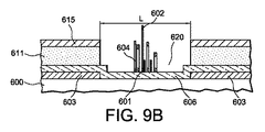
600 支持材
601 障壁層
602 触媒層
603 カソード電極
604 ナノ構造物
605 抽出ゲート
606 抵抗層
611 絶縁層
615 金属層
620 穴
700 支持材
701 障壁層
703 導電層
704 ナノ構造物
706 抵抗層
711 絶縁層
715 金属層
720 穴
803 カソード
811 絶縁層
815 ゲート電極
Claims (21)
- 支持材上のナノ構造物(104;404;604;704;804)の製造方法であって、
面の1つの上に表面層(101;401;601;701;801)を備える支持材を供給するステップと、
触媒層によって覆われた前記表面層の領域及び前記触媒層によって覆われていない前記表面層の領域を露出するパターンに従って構造化された触媒層(102;202;402;602;702;802)によって前記表面層を覆うステップと、
前記触媒層によって覆われていない領域における前記表面層(101;401;601;701;801)の厚さをエッチングするステップと、
前記触媒層によって覆われた表面層の領域上に前記ナノ構造物(104;404;604;704;804)を選択的に成長させるステップと、を含み、
前記触媒層が前記表面層の厚さをエッチングするためのマスクとして、かつ前記ナノ構造物の選択的な成長の触媒として働くように前記触媒層が構造化され、
前記触媒層は、前記表面層上の触媒膜の断片化によって得られたパターンに従って構造化され、
前記表面層上の触媒膜は、前記触媒膜の温度を上昇させることによって断片化されることを特徴とするナノ構造物の製造方法。 - 前記表面層は、障壁層であることを特徴とする請求項1に記載のナノ構造物の製造方法。
- 前記表面層は、導電性又は半導電性材料で作製され、
前記ナノ構造物は、導電性又は半導電性材料で作製されることを特徴とする請求項1又は2に記載のナノ構造物の製造方法。 - 前記支持材は、前記表面層(401;601;701;801)を支持する面上に抵抗層(406;606;706;806)を備えることを特徴とする請求項1から3のいずれか一項に記載のナノ構造物の製造方法。
- 前記支持材は、前記抵抗層と接触する導電材料で作製される層(402;602;702;802)を備えることを特徴とする請求項4に記載のナノ構造物の製造方法。
- 前記抵抗層の厚さの少なくとも一部は、前記表面層がエッチングされる領域においてエッチングされることを特徴とする請求項4又は5に記載のナノ構造物の製造方法。
- 前記触媒膜の温度は、焼なましによって全体的に上昇することを特徴とする請求項1から6のいずれか一項に記載のナノ構造物の製造方法。
- 前記触媒膜の温度の上昇は、レーザー照射によって、又は、プラズマ効果によって、前記表面層上に局所的であることを特徴とする請求項1から6のいずれか一項に記載のナノ構造物の製造方法。
- 前記表面層は、前記触媒膜の前記断片化を促進する材料で作製されることを特徴とする請求項1から8のいずれか一項に記載のナノ構造物の製造方法。
- 前記構造化された触媒層のパターンは、前記表面層のエッチングステップを実行する前に調整されることを特徴とする請求項1から9のいずれか一項に記載のナノ構造物の製造方法。
- 前記触媒層のパターンは、前記触媒層をエッチングすることによって調整されることを特徴とする請求項10に記載のナノ構造物の製造方法。
- 前記触媒層のパターンは、前記表面層のエッチングステップを実行した後に、前記触媒層のエッチングによって調整されることを特徴とする請求項1から11のいずれか一項に記載のナノ構造物の製造方法。
- 前記触媒上のナノ構造物の選択的な成長は、化学気相堆積(CVD)によってなされることを特徴とする請求項1から12のいずれか一項に記載のナノ構造物の製造方法。
- 前記表面層のエッチングステップは、前記ナノ構造物の選択的な成長のステップの後に、実行されることを特徴とする請求項1から13のいずれか一項に記載のナノ構造物の製造方法。
- 前記表面層は、前記支持材に向かう前記触媒の拡散への障壁層であることを特徴とする請求項14に記載のナノ構造物の製造方法。
- カソード構造物であって、
カソード(603;703;803)を形成する導電層と、
触媒の拡散への障壁層(601;701;801)の上で構造化された触媒層(602;702;802)から形成される電子放出ナノ構造物(604;704;804)を備える少なくとも1つの電子放出領域と、を備え、
前記触媒層が前記障壁層のエッチングプロセスのために、及び前記ナノ構造物を選択的に成長するために、前記障壁層を覆い、
前記障壁層は、抵抗層によって支持され、
前記ナノ構造物は、前記障壁層及び前記抵抗層を介して、前記カソードを形成する前記導電層に電気的に接続され、
前記ナノ構造物によって放出される電子を抽出するための抽出ゲート(615;715;815)を形成する金属層、を備え、
前記ナノ構造物は、電気的に独立したナノ構造物であることを特徴とする、カソード構造物。 - 前記カソード(703)を形成する導電層は、
電気的絶縁材料で作製される層(711)中に形成される少なくとも1つの穴の底部に配置され、
前記カソードを形成する前記導電層は前記抵抗層を支持して、前記ナノ構造物(704)を備える前記電子放出領域をそれ自体で支持して、電気的絶縁材料で作製される前記層(711)の上面は、前記抽出ゲート(715)を形成する金属層を支持する、請求項16に記載のカソード構造物。 - 前記カソード(603)を形成する前記導電層、及びナノ構造物(604)を備える前記電子放出領域は、一方を他方の側部に配置して、前記抵抗層(606)によって離隔され、
前記抽出ゲート(615)を形成する前記金属層は、前記カソード(603)を形成する前記導電層から電気的絶縁層(611)によって離隔される、請求項16に記載のカソード構造物。 - 電気的絶縁材料層(811)は、2つの部分に分けられる抽出ゲート(815)を形成していて、前記電気的絶縁材料層(811)の上面上に位置する前記カソード(803)を形成する導電材料の層を囲む前記金属層をその上面上で支持して、
前記カソード(803)を形成する前記導電層は、それ自体で電子放出領域を支持する抵抗層を支持する請求項16に記載のカソード構造物。 - 発光層によって覆われる、カソード及びアノードを備える装置であって、
前記アノードは、前記カソードに対向して配置され、前記アノード及び前記カソードは、真空が生成される空間によって離隔され、
前記カソードは、請求項3から15のいずれか一項に記載の方法に従って作製される電気的に独立したナノ構造物を備えることを特徴とする、装置。 - 請求項16から19のいずれか一項に記載の少なくとも1つのカソード構造物を備えていることを特徴とする電界放出フラットスクリーン。
Applications Claiming Priority (3)
| Application Number | Priority Date | Filing Date | Title |
|---|---|---|---|
| FR0551412A FR2886284B1 (fr) | 2005-05-30 | 2005-05-30 | Procede de realisation de nanostructures |
| FR0551412 | 2005-05-30 | ||
| PCT/FR2006/050489 WO2007003826A2 (fr) | 2005-05-30 | 2006-05-29 | Procede de realisation de nanostructures |
Publications (2)
| Publication Number | Publication Date |
|---|---|
| JP2008546146A JP2008546146A (ja) | 2008-12-18 |
| JP5247438B2 true JP5247438B2 (ja) | 2013-07-24 |
Family
ID=35520555
Family Applications (2)
| Application Number | Title | Priority Date | Filing Date |
|---|---|---|---|
| JP2008514165A Active JP5247438B2 (ja) | 2005-05-30 | 2006-05-29 | ナノ構造物の製造方法 |
| JP2008514166A Pending JP2008543008A (ja) | 2005-05-30 | 2006-05-29 | 放出陰極の製造方法 |
Family Applications After (1)
| Application Number | Title | Priority Date | Filing Date |
|---|---|---|---|
| JP2008514166A Pending JP2008543008A (ja) | 2005-05-30 | 2006-05-29 | 放出陰極の製造方法 |
Country Status (5)
| Country | Link |
|---|---|
| US (2) | US7993703B2 (ja) |
| EP (2) | EP1885648B1 (ja) |
| JP (2) | JP5247438B2 (ja) |
| FR (1) | FR2886284B1 (ja) |
| WO (2) | WO2007026086A2 (ja) |
Families Citing this family (15)
| Publication number | Priority date | Publication date | Assignee | Title |
|---|---|---|---|---|
| FR2873852B1 (fr) | 2004-07-28 | 2011-06-24 | Commissariat Energie Atomique | Structure de cathode a haute resolution |
| US8172633B2 (en) * | 2006-04-05 | 2012-05-08 | Industry Academic Cooperation Fundation of Kyunghee University | Field emission display and manufacturing method of the same having selective array of electron emission source |
| KR100803194B1 (ko) * | 2006-06-30 | 2008-02-14 | 삼성에스디아이 주식회사 | 탄소나노튜브 구조체 형성방법 |
| CA2671663A1 (en) | 2006-12-19 | 2008-06-26 | Basf Coatings Ag | Coating compositions with high scratch resistance and weathering stability |
| DE102007061854A1 (de) | 2007-12-19 | 2009-06-25 | Basf Coatings Ag | Beschichtungsmittel mit hoher Kratzbeständigkeit und Witterungsstabilität |
| DE102007061855A1 (de) | 2007-12-19 | 2009-06-25 | Basf Coatings Ag | Beschichtungsmittel mit hoher Kratzbeständigkeit und Witterungsstabilität |
| DE102007061856A1 (de) | 2007-12-19 | 2009-06-25 | Basf Coatings Ag | Beschichtungsmittel mit hoher Kratzbeständigkeit und Witterungsstabilität |
| JP5187689B2 (ja) * | 2008-08-08 | 2013-04-24 | 学校法人 関西大学 | ナノワイヤ構造体、ナノワイヤ結合体、およびその製造方法 |
| JP5572944B2 (ja) * | 2008-12-18 | 2014-08-20 | 富士通株式会社 | 配線構造体の製造方法及び配線構造体 |
| DE102009024103A1 (de) | 2009-06-06 | 2010-12-09 | Basf Coatings Gmbh | Beschichtungsmittel und daraus hergestellte Beschichtungen mit hoher Kratzfestigkeit und hoher Kocherstabilität |
| CN102064063B (zh) * | 2010-12-24 | 2012-08-29 | 清华大学 | 场发射阴极装置及其制备方法 |
| EP2541581A1 (en) * | 2011-06-29 | 2013-01-02 | Khalid Waqas | Device comprising nanostructures and method of manufacturing thereof |
| WO2013037951A1 (en) * | 2011-09-16 | 2013-03-21 | Danmarks Tekniske Universitet | Catalyst deposition for the preparation of carbon nanotubes |
| CN105984862B (zh) * | 2015-02-16 | 2018-08-28 | 北京大学深圳研究生院 | 用于生长碳纳米管的方法 |
| JP7556246B2 (ja) | 2020-09-23 | 2024-09-26 | セイコーエプソン株式会社 | 発光装置、発光装置の製造方法およびプロジェクター |
Family Cites Families (46)
| Publication number | Priority date | Publication date | Assignee | Title |
|---|---|---|---|---|
| FR2593953B1 (fr) | 1986-01-24 | 1988-04-29 | Commissariat Energie Atomique | Procede de fabrication d'un dispositif de visualisation par cathodoluminescence excitee par emission de champ |
| FR2687839B1 (fr) * | 1992-02-26 | 1994-04-08 | Commissariat A Energie Atomique | Source d'electrons a cathodes emissives a micropointes et dispositif de visualisation par cathodoluminescence excitee par emission de champ utilisant cette source. |
| EP0700063A1 (en) * | 1994-08-31 | 1996-03-06 | International Business Machines Corporation | Structure and method for fabricating of a field emission device |
| JPH08115654A (ja) * | 1994-10-14 | 1996-05-07 | Sony Corp | 粒子放出装置、電界放出型装置及びこれらの製造方法 |
| US5872422A (en) | 1995-12-20 | 1999-02-16 | Advanced Technology Materials, Inc. | Carbon fiber-based field emission devices |
| JP2000067736A (ja) * | 1998-08-14 | 2000-03-03 | Sony Corp | 電子放出素子およびその製造方法、ならびにこれを用いたディスプレイ装置 |
| JP2000123713A (ja) * | 1998-10-15 | 2000-04-28 | Sony Corp | 電子放出素子およびその製造方法、ならびにこれを用いたディスプレイ装置 |
| JP2000323012A (ja) * | 1999-05-10 | 2000-11-24 | Futaba Corp | 電界放出素子 |
| JP2001023506A (ja) * | 1999-07-07 | 2001-01-26 | Sony Corp | 電子放出源およびその製造方法ならびにディスプレイ装置 |
| US6062931A (en) * | 1999-09-01 | 2000-05-16 | Industrial Technology Research Institute | Carbon nanotube emitter with triode structure |
| FR2798507B1 (fr) | 1999-09-09 | 2006-06-02 | Commissariat Energie Atomique | Dispositif permettant de produire un champ electrique module au niveau d'une electrode et son application aux ecrans plats a emission de champ |
| FR2798508B1 (fr) | 1999-09-09 | 2001-10-05 | Commissariat Energie Atomique | Dispositif permettant de produire un champ electrique module au niveau d'une electrode et son application aux ecrans plats a emission de champ |
| KR100480773B1 (ko) * | 2000-01-07 | 2005-04-06 | 삼성에스디아이 주식회사 | 카본 나노 튜브를 이용한 3극 전계방출소자의 제작방법 |
| JP2002117791A (ja) * | 2000-10-06 | 2002-04-19 | Hitachi Ltd | 画像表示装置 |
| JP3737696B2 (ja) * | 2000-11-17 | 2006-01-18 | 株式会社東芝 | 横型の電界放出型冷陰極装置の製造方法 |
| CA2442985C (en) * | 2001-03-30 | 2016-05-31 | The Regents Of The University Of California | Methods of fabricating nanostructures and nanowires and devices fabricated therefrom |
| US6541906B2 (en) * | 2001-05-23 | 2003-04-01 | Industrial Technology Research Institute | Field emission display panel equipped with a dual-layer cathode and an anode on the same substrate and method for fabrication |
| US6920680B2 (en) * | 2001-08-28 | 2005-07-26 | Motorola, Inc. | Method of making vacuum microelectronic device |
| FR2829873B1 (fr) * | 2001-09-20 | 2006-09-01 | Thales Sa | Procede de croissance localisee de nanotubes et procede de fabrication de cathode autoalignee utilisant le procede de croissance de nanotubes |
| JP2003115259A (ja) * | 2001-10-03 | 2003-04-18 | Sony Corp | 電子放出装置及びその製造方法、冷陰極電界電子放出素子及びその製造方法、冷陰極電界電子放出表示装置及びその製造方法、並びに、薄膜のエッチング方法 |
| JP2003115257A (ja) * | 2001-10-03 | 2003-04-18 | Sony Corp | 冷陰極電界電子放出素子の製造方法、及び、冷陰極電界電子放出表示装置の製造方法 |
| KR100449071B1 (ko) * | 2001-12-28 | 2004-09-18 | 한국전자통신연구원 | 전계 방출 소자용 캐소드 |
| FR2836280B1 (fr) | 2002-02-19 | 2004-04-02 | Commissariat Energie Atomique | Structure de cathode a couche emissive formee sur une couche resistive |
| FR2836279B1 (fr) * | 2002-02-19 | 2004-09-24 | Commissariat Energie Atomique | Structure de cathode pour ecran emissif |
| CN100407362C (zh) * | 2002-04-12 | 2008-07-30 | 三星Sdi株式会社 | 场发射显示器 |
| GB2389959B (en) * | 2002-06-19 | 2006-06-14 | Univ Dundee | Improved field emission device |
| JP3890470B2 (ja) * | 2002-07-16 | 2007-03-07 | 日立造船株式会社 | カーボンナノチューブを用いた電子放出素子用電極材料およびその製造方法 |
| US7175494B1 (en) * | 2002-08-22 | 2007-02-13 | Cdream Corporation | Forming carbon nanotubes at lower temperatures suitable for an electron-emitting device |
| US6803708B2 (en) * | 2002-08-22 | 2004-10-12 | Cdream Display Corporation | Barrier metal layer for a carbon nanotube flat panel display |
| US20040037972A1 (en) * | 2002-08-22 | 2004-02-26 | Kang Simon | Patterned granulized catalyst layer suitable for electron-emitting device, and associated fabrication method |
| US6984535B2 (en) * | 2002-12-20 | 2006-01-10 | Cdream Corporation | Selective etching of a protective layer to form a catalyst layer for an electron-emitting device |
| US7064475B2 (en) * | 2002-12-26 | 2006-06-20 | Canon Kabushiki Kaisha | Electron source structure covered with resistance film |
| KR100884527B1 (ko) * | 2003-01-07 | 2009-02-18 | 삼성에스디아이 주식회사 | 전계 방출 표시장치 |
| EP1582501A4 (en) * | 2003-01-09 | 2009-01-28 | Sony Corp | PROCESS FOR TUBE-LIKE CARBON MOLECULAR AND TUBE SHAPED CARBON MOLECULE, METHOD FOR RECORDING DEVICE AND RECORDING DEVICE, METHOD FOR FIELD ELECTRON EMISSION ELEMENT AND FIELD ELECTRON EMISSION ELEMENT AND METHOD FOR DISPLAY UNIT AND DISPLAY UNIT |
| JP3900094B2 (ja) * | 2003-03-14 | 2007-04-04 | 三菱電機株式会社 | 電子放出素子及びその製造方法ならびに表示装置 |
| JP2004281308A (ja) * | 2003-03-18 | 2004-10-07 | Mitsubishi Electric Corp | 冷陰極電子源及びその製造方法 |
| US7521851B2 (en) * | 2003-03-24 | 2009-04-21 | Zhidan L Tolt | Electron emitting composite based on regulated nano-structures and a cold electron source using the composite |
| JP4083611B2 (ja) * | 2003-03-25 | 2008-04-30 | 三菱電機株式会社 | 冷陰極電子源の製造方法 |
| JP2004362960A (ja) * | 2003-06-05 | 2004-12-24 | Akio Hiraki | 電子放出素子およびその製造方法 |
| JP2005078850A (ja) * | 2003-08-28 | 2005-03-24 | Ulvac Japan Ltd | 炭素系超微細冷陰極およびその製造方法 |
| JP4448356B2 (ja) * | 2004-03-26 | 2010-04-07 | 富士通株式会社 | 半導体装置およびその製造方法 |
| US20050236963A1 (en) * | 2004-04-15 | 2005-10-27 | Kang Sung G | Emitter structure with a protected gate electrode for an electron-emitting device |
| FR2873852B1 (fr) * | 2004-07-28 | 2011-06-24 | Commissariat Energie Atomique | Structure de cathode a haute resolution |
| KR100682863B1 (ko) * | 2005-02-19 | 2007-02-15 | 삼성에스디아이 주식회사 | 탄소나노튜브 구조체 및 그 제조방법과, 탄소나노튜브 구조체를 이용한 전계방출소자 및 그 제조방법 |
| KR100697656B1 (ko) * | 2005-04-28 | 2007-03-22 | 이승호 | 다중 전자 공급원을 구비한 평면 발광 소자 |
| FR2897718B1 (fr) | 2006-02-22 | 2008-10-17 | Commissariat Energie Atomique | Structure de cathode a nanotubes pour ecran emissif |
-
2005
- 2005-05-30 FR FR0551412A patent/FR2886284B1/fr not_active Expired - Fee Related
-
2006
- 2006-05-29 JP JP2008514165A patent/JP5247438B2/ja active Active
- 2006-05-29 EP EP06794468.6A patent/EP1885648B1/fr not_active Not-in-force
- 2006-05-29 EP EP06820247A patent/EP1885649A2/fr not_active Withdrawn
- 2006-05-29 WO PCT/FR2006/050490 patent/WO2007026086A2/fr not_active Application Discontinuation
- 2006-05-29 WO PCT/FR2006/050489 patent/WO2007003826A2/fr not_active Application Discontinuation
- 2006-05-29 JP JP2008514166A patent/JP2008543008A/ja active Pending
- 2006-05-29 US US11/915,238 patent/US7993703B2/en not_active Expired - Fee Related
- 2006-05-29 US US11/915,222 patent/US7785164B2/en not_active Expired - Fee Related
Also Published As
| Publication number | Publication date |
|---|---|
| EP1885649A2 (fr) | 2008-02-13 |
| JP2008546146A (ja) | 2008-12-18 |
| US20080194168A1 (en) | 2008-08-14 |
| WO2007026086A2 (fr) | 2007-03-08 |
| FR2886284B1 (fr) | 2007-06-29 |
| WO2007026086A3 (fr) | 2007-05-31 |
| EP1885648B1 (fr) | 2018-08-29 |
| EP1885648A2 (fr) | 2008-02-13 |
| US7993703B2 (en) | 2011-08-09 |
| WO2007003826A2 (fr) | 2007-01-11 |
| US20080197766A1 (en) | 2008-08-21 |
| US7785164B2 (en) | 2010-08-31 |
| WO2007003826A3 (fr) | 2007-04-12 |
| FR2886284A1 (fr) | 2006-12-01 |
| JP2008543008A (ja) | 2008-11-27 |
Similar Documents
| Publication | Publication Date | Title |
|---|---|---|
| JP5247438B2 (ja) | ナノ構造物の製造方法 | |
| US6568979B2 (en) | Method of manufacturing a low gate current field emitter cell and array with vertical thin-film-edge emitter | |
| JP4648807B2 (ja) | カーボンナノチューブエミッタ及びその製造方法とそれを応用した電界放出素子及びその製造方法 | |
| US6890233B2 (en) | Method of making low gate current multilayer emitter with vertical thin-film-edge multilayer emitter | |
| JP2001236879A (ja) | カーボンナノチューブを用いた3極電界放出素子の製造方法 | |
| JP2011508189A (ja) | 基板の表面上に構成された微細パターンの表面上への炭素ナノファイバーの集合的な作製方法、および微細パターンの表面上にナノファイバーを含む構造 | |
| WO2003025966A1 (fr) | Procede de croissance localisee de nanotubes et procede de fabrication de cathode autoalignee utilisant le procede de croissance de nanotubes | |
| JP4611228B2 (ja) | 電界電子放出装置およびその製造方法 | |
| CN101552166B (zh) | 场致发射装置及其制造方法 | |
| JP4456891B2 (ja) | カソード基板及びその作製方法 | |
| JP4703270B2 (ja) | ナノ構造体群を用いた電子素子 | |
| JP2006519693A (ja) | 電界放出で特にフラット表示面を製造するために構築された触媒 | |
| JP2000353467A (ja) | 冷陰極装置の製造方法 | |
| JP2006196364A (ja) | 電界電子放出素子、およびその製造方法 | |
| JP4476090B2 (ja) | 電子放出装置の製造方法 | |
| JP4997750B2 (ja) | カーボンナノチューブを用いた電子素子及びその製造方法 | |
| JP2006294387A (ja) | ナノカーボンエミッタ及びその製造方法 | |
| JP4590631B2 (ja) | フィールドエミッタアレイ及びその製造方法 | |
| JP4371976B2 (ja) | 電界電子放出装置 | |
| JP2007513477A (ja) | 電界放出デバイス | |
| JP4875432B2 (ja) | 冷陰極素子の製造方法及びこれを用いた冷陰極素子 | |
| JP2008226825A (ja) | 電子放出素子、これを備えた電子放出ディスプレイ装置、及びその製造方法 | |
| KR100934228B1 (ko) | 진공 채널 트랜지스터 및 그 제조방법 | |
| WO2010109454A1 (en) | Nanotube-based electron emission device and method for fabrication thereof | |
| JP2005150091A (ja) | カーボンナノファイバを形成しやすい金属板およびナノカーボンエミッタ |
Legal Events
| Date | Code | Title | Description |
|---|---|---|---|
| A621 | Written request for application examination |
Free format text: JAPANESE INTERMEDIATE CODE: A621 Effective date: 20090528 |
|
| A977 | Report on retrieval |
Free format text: JAPANESE INTERMEDIATE CODE: A971007 Effective date: 20110930 |
|
| A131 | Notification of reasons for refusal |
Free format text: JAPANESE INTERMEDIATE CODE: A131 Effective date: 20111004 |
|
| A601 | Written request for extension of time |
Free format text: JAPANESE INTERMEDIATE CODE: A601 Effective date: 20111228 |
|
| A602 | Written permission of extension of time |
Free format text: JAPANESE INTERMEDIATE CODE: A602 Effective date: 20120111 |
|
| A601 | Written request for extension of time |
Free format text: JAPANESE INTERMEDIATE CODE: A601 Effective date: 20120126 |
|
| A602 | Written permission of extension of time |
Free format text: JAPANESE INTERMEDIATE CODE: A602 Effective date: 20120202 |
|
| A521 | Request for written amendment filed |
Free format text: JAPANESE INTERMEDIATE CODE: A523 Effective date: 20120302 |
|
| A131 | Notification of reasons for refusal |
Free format text: JAPANESE INTERMEDIATE CODE: A131 Effective date: 20120911 |
|
| A601 | Written request for extension of time |
Free format text: JAPANESE INTERMEDIATE CODE: A601 Effective date: 20121203 |
|
| A602 | Written permission of extension of time |
Free format text: JAPANESE INTERMEDIATE CODE: A602 Effective date: 20121210 |
|
| A601 | Written request for extension of time |
Free format text: JAPANESE INTERMEDIATE CODE: A601 Effective date: 20130108 |
|
| A602 | Written permission of extension of time |
Free format text: JAPANESE INTERMEDIATE CODE: A602 Effective date: 20130116 |
|
| A521 | Request for written amendment filed |
Free format text: JAPANESE INTERMEDIATE CODE: A523 Effective date: 20130212 |
|
| TRDD | Decision of grant or rejection written | ||
| A01 | Written decision to grant a patent or to grant a registration (utility model) |
Free format text: JAPANESE INTERMEDIATE CODE: A01 Effective date: 20130312 |
|
| A61 | First payment of annual fees (during grant procedure) |
Free format text: JAPANESE INTERMEDIATE CODE: A61 Effective date: 20130409 |
|
| R150 | Certificate of patent or registration of utility model |
Ref document number: 5247438 Country of ref document: JP Free format text: JAPANESE INTERMEDIATE CODE: R150 Free format text: JAPANESE INTERMEDIATE CODE: R150 |
|
| FPAY | Renewal fee payment (event date is renewal date of database) |
Free format text: PAYMENT UNTIL: 20160419 Year of fee payment: 3 |
|
| R250 | Receipt of annual fees |
Free format text: JAPANESE INTERMEDIATE CODE: R250 |
|
| R250 | Receipt of annual fees |
Free format text: JAPANESE INTERMEDIATE CODE: R250 |
|
| R250 | Receipt of annual fees |
Free format text: JAPANESE INTERMEDIATE CODE: R250 |
|
| R250 | Receipt of annual fees |
Free format text: JAPANESE INTERMEDIATE CODE: R250 |
|
| R250 | Receipt of annual fees |
Free format text: JAPANESE INTERMEDIATE CODE: R250 |