JP5218058B2 - 半導体装置およびその製造方法 - Google Patents
半導体装置およびその製造方法 Download PDFInfo
- Publication number
- JP5218058B2 JP5218058B2 JP2008534206A JP2008534206A JP5218058B2 JP 5218058 B2 JP5218058 B2 JP 5218058B2 JP 2008534206 A JP2008534206 A JP 2008534206A JP 2008534206 A JP2008534206 A JP 2008534206A JP 5218058 B2 JP5218058 B2 JP 5218058B2
- Authority
- JP
- Japan
- Prior art keywords
- solid
- semiconductor device
- state imaging
- adhesive
- gold
- Prior art date
- Legal status (The legal status is an assumption and is not a legal conclusion. Google has not performed a legal analysis and makes no representation as to the accuracy of the status listed.)
- Expired - Fee Related
Links
- 239000004065 semiconductor Substances 0.000 title claims abstract description 160
- 238000004519 manufacturing process Methods 0.000 title claims description 17
- 238000003384 imaging method Methods 0.000 claims abstract description 110
- 239000000853 adhesive Substances 0.000 claims abstract description 75
- 230000001070 adhesive effect Effects 0.000 claims abstract description 66
- 238000007789 sealing Methods 0.000 claims description 56
- 239000000758 substrate Substances 0.000 claims description 37
- 238000000034 method Methods 0.000 claims description 32
- 230000015572 biosynthetic process Effects 0.000 claims description 9
- PCHJSUWPFVWCPO-UHFFFAOYSA-N gold Chemical compound [Au] PCHJSUWPFVWCPO-UHFFFAOYSA-N 0.000 abstract description 122
- 239000010931 gold Substances 0.000 abstract description 66
- 229910052737 gold Inorganic materials 0.000 abstract description 64
- 239000007787 solid Substances 0.000 abstract description 6
- 239000011521 glass Substances 0.000 description 48
- 230000003287 optical effect Effects 0.000 description 34
- 229920005989 resin Polymers 0.000 description 31
- 239000011347 resin Substances 0.000 description 31
- 238000010586 diagram Methods 0.000 description 28
- 229910000679 solder Inorganic materials 0.000 description 11
- 239000000463 material Substances 0.000 description 7
- 230000000694 effects Effects 0.000 description 6
- 239000002184 metal Substances 0.000 description 6
- 229910052751 metal Inorganic materials 0.000 description 6
- 238000000926 separation method Methods 0.000 description 3
- 230000006835 compression Effects 0.000 description 2
- 238000007906 compression Methods 0.000 description 2
- 238000002955 isolation Methods 0.000 description 2
- 238000012986 modification Methods 0.000 description 2
- 230000004048 modification Effects 0.000 description 2
- XLYOFNOQVPJJNP-UHFFFAOYSA-N water Substances O XLYOFNOQVPJJNP-UHFFFAOYSA-N 0.000 description 2
- 239000003522 acrylic cement Substances 0.000 description 1
- 238000005452 bending Methods 0.000 description 1
- 239000011248 coating agent Substances 0.000 description 1
- 238000000576 coating method Methods 0.000 description 1
- 230000000052 comparative effect Effects 0.000 description 1
- 230000000295 complement effect Effects 0.000 description 1
- 238000005516 engineering process Methods 0.000 description 1
- 229920006332 epoxy adhesive Polymers 0.000 description 1
- 238000002347 injection Methods 0.000 description 1
- 239000007924 injection Substances 0.000 description 1
- 229910044991 metal oxide Inorganic materials 0.000 description 1
- 150000004706 metal oxides Chemical class 0.000 description 1
- 238000000465 moulding Methods 0.000 description 1
- 230000002093 peripheral effect Effects 0.000 description 1
- 238000007747 plating Methods 0.000 description 1
- 239000003566 sealing material Substances 0.000 description 1
- 229910052710 silicon Inorganic materials 0.000 description 1
- 239000010703 silicon Substances 0.000 description 1
- 229920001187 thermosetting polymer Polymers 0.000 description 1
Images


Classifications
-
- H—ELECTRICITY
- H10—SEMICONDUCTOR DEVICES; ELECTRIC SOLID-STATE DEVICES NOT OTHERWISE PROVIDED FOR
- H10F—INORGANIC SEMICONDUCTOR DEVICES SENSITIVE TO INFRARED RADIATION, LIGHT, ELECTROMAGNETIC RADIATION OF SHORTER WAVELENGTH OR CORPUSCULAR RADIATION
- H10F39/00—Integrated devices, or assemblies of multiple devices, comprising at least one element covered by group H10F30/00, e.g. radiation detectors comprising photodiode arrays
- H10F39/80—Constructional details of image sensors
- H10F39/803—Pixels having integrated switching, control, storage or amplification elements
- H10F39/8037—Pixels having integrated switching, control, storage or amplification elements the integrated elements comprising a transistor
-
- H—ELECTRICITY
- H01—ELECTRIC ELEMENTS
- H01L—SEMICONDUCTOR DEVICES NOT COVERED BY CLASS H10
- H01L24/00—Arrangements for connecting or disconnecting semiconductor or solid-state bodies; Methods or apparatus related thereto
- H01L24/93—Batch processes
- H01L24/95—Batch processes at chip-level, i.e. with connecting carried out on a plurality of singulated devices, i.e. on diced chips
- H01L24/97—Batch processes at chip-level, i.e. with connecting carried out on a plurality of singulated devices, i.e. on diced chips the devices being connected to a common substrate, e.g. interposer, said common substrate being separable into individual assemblies after connecting
-
- H—ELECTRICITY
- H10—SEMICONDUCTOR DEVICES; ELECTRIC SOLID-STATE DEVICES NOT OTHERWISE PROVIDED FOR
- H10F—INORGANIC SEMICONDUCTOR DEVICES SENSITIVE TO INFRARED RADIATION, LIGHT, ELECTROMAGNETIC RADIATION OF SHORTER WAVELENGTH OR CORPUSCULAR RADIATION
- H10F39/00—Integrated devices, or assemblies of multiple devices, comprising at least one element covered by group H10F30/00, e.g. radiation detectors comprising photodiode arrays
- H10F39/80—Constructional details of image sensors
- H10F39/804—Containers or encapsulations
-
- H—ELECTRICITY
- H10—SEMICONDUCTOR DEVICES; ELECTRIC SOLID-STATE DEVICES NOT OTHERWISE PROVIDED FOR
- H10F—INORGANIC SEMICONDUCTOR DEVICES SENSITIVE TO INFRARED RADIATION, LIGHT, ELECTROMAGNETIC RADIATION OF SHORTER WAVELENGTH OR CORPUSCULAR RADIATION
- H10F39/00—Integrated devices, or assemblies of multiple devices, comprising at least one element covered by group H10F30/00, e.g. radiation detectors comprising photodiode arrays
- H10F39/80—Constructional details of image sensors
- H10F39/806—Optical elements or arrangements associated with the image sensors
-
- H—ELECTRICITY
- H10—SEMICONDUCTOR DEVICES; ELECTRIC SOLID-STATE DEVICES NOT OTHERWISE PROVIDED FOR
- H10F—INORGANIC SEMICONDUCTOR DEVICES SENSITIVE TO INFRARED RADIATION, LIGHT, ELECTROMAGNETIC RADIATION OF SHORTER WAVELENGTH OR CORPUSCULAR RADIATION
- H10F77/00—Constructional details of devices covered by this subclass
- H10F77/50—Encapsulations or containers
-
- H—ELECTRICITY
- H01—ELECTRIC ELEMENTS
- H01L—SEMICONDUCTOR DEVICES NOT COVERED BY CLASS H10
- H01L2224/00—Indexing scheme for arrangements for connecting or disconnecting semiconductor or solid-state bodies and methods related thereto as covered by H01L24/00
- H01L2224/01—Means for bonding being attached to, or being formed on, the surface to be connected, e.g. chip-to-package, die-attach, "first-level" interconnects; Manufacturing methods related thereto
- H01L2224/26—Layer connectors, e.g. plate connectors, solder or adhesive layers; Manufacturing methods related thereto
- H01L2224/31—Structure, shape, material or disposition of the layer connectors after the connecting process
- H01L2224/32—Structure, shape, material or disposition of the layer connectors after the connecting process of an individual layer connector
- H01L2224/321—Disposition
- H01L2224/32151—Disposition the layer connector connecting between a semiconductor or solid-state body and an item not being a semiconductor or solid-state body, e.g. chip-to-substrate, chip-to-passive
- H01L2224/32221—Disposition the layer connector connecting between a semiconductor or solid-state body and an item not being a semiconductor or solid-state body, e.g. chip-to-substrate, chip-to-passive the body and the item being stacked
- H01L2224/32225—Disposition the layer connector connecting between a semiconductor or solid-state body and an item not being a semiconductor or solid-state body, e.g. chip-to-substrate, chip-to-passive the body and the item being stacked the item being non-metallic, e.g. insulating substrate with or without metallisation
-
- H—ELECTRICITY
- H01—ELECTRIC ELEMENTS
- H01L—SEMICONDUCTOR DEVICES NOT COVERED BY CLASS H10
- H01L2224/00—Indexing scheme for arrangements for connecting or disconnecting semiconductor or solid-state bodies and methods related thereto as covered by H01L24/00
- H01L2224/01—Means for bonding being attached to, or being formed on, the surface to be connected, e.g. chip-to-package, die-attach, "first-level" interconnects; Manufacturing methods related thereto
- H01L2224/42—Wire connectors; Manufacturing methods related thereto
- H01L2224/44—Structure, shape, material or disposition of the wire connectors prior to the connecting process
- H01L2224/45—Structure, shape, material or disposition of the wire connectors prior to the connecting process of an individual wire connector
- H01L2224/45001—Core members of the connector
- H01L2224/45099—Material
- H01L2224/451—Material with a principal constituent of the material being a metal or a metalloid, e.g. boron (B), silicon (Si), germanium (Ge), arsenic (As), antimony (Sb), tellurium (Te) and polonium (Po), and alloys thereof
- H01L2224/45138—Material with a principal constituent of the material being a metal or a metalloid, e.g. boron (B), silicon (Si), germanium (Ge), arsenic (As), antimony (Sb), tellurium (Te) and polonium (Po), and alloys thereof the principal constituent melting at a temperature of greater than or equal to 950°C and less than 1550°C
- H01L2224/45144—Gold (Au) as principal constituent
-
- H—ELECTRICITY
- H01—ELECTRIC ELEMENTS
- H01L—SEMICONDUCTOR DEVICES NOT COVERED BY CLASS H10
- H01L2224/00—Indexing scheme for arrangements for connecting or disconnecting semiconductor or solid-state bodies and methods related thereto as covered by H01L24/00
- H01L2224/01—Means for bonding being attached to, or being formed on, the surface to be connected, e.g. chip-to-package, die-attach, "first-level" interconnects; Manufacturing methods related thereto
- H01L2224/42—Wire connectors; Manufacturing methods related thereto
- H01L2224/47—Structure, shape, material or disposition of the wire connectors after the connecting process
- H01L2224/48—Structure, shape, material or disposition of the wire connectors after the connecting process of an individual wire connector
- H01L2224/481—Disposition
- H01L2224/48151—Connecting between a semiconductor or solid-state body and an item not being a semiconductor or solid-state body, e.g. chip-to-substrate, chip-to-passive
- H01L2224/48221—Connecting between a semiconductor or solid-state body and an item not being a semiconductor or solid-state body, e.g. chip-to-substrate, chip-to-passive the body and the item being stacked
- H01L2224/48225—Connecting between a semiconductor or solid-state body and an item not being a semiconductor or solid-state body, e.g. chip-to-substrate, chip-to-passive the body and the item being stacked the item being non-metallic, e.g. insulating substrate with or without metallisation
- H01L2224/48227—Connecting between a semiconductor or solid-state body and an item not being a semiconductor or solid-state body, e.g. chip-to-substrate, chip-to-passive the body and the item being stacked the item being non-metallic, e.g. insulating substrate with or without metallisation connecting the wire to a bond pad of the item
-
- H—ELECTRICITY
- H01—ELECTRIC ELEMENTS
- H01L—SEMICONDUCTOR DEVICES NOT COVERED BY CLASS H10
- H01L2224/00—Indexing scheme for arrangements for connecting or disconnecting semiconductor or solid-state bodies and methods related thereto as covered by H01L24/00
- H01L2224/01—Means for bonding being attached to, or being formed on, the surface to be connected, e.g. chip-to-package, die-attach, "first-level" interconnects; Manufacturing methods related thereto
- H01L2224/42—Wire connectors; Manufacturing methods related thereto
- H01L2224/47—Structure, shape, material or disposition of the wire connectors after the connecting process
- H01L2224/48—Structure, shape, material or disposition of the wire connectors after the connecting process of an individual wire connector
- H01L2224/484—Connecting portions
- H01L2224/48463—Connecting portions the connecting portion on the bonding area of the semiconductor or solid-state body being a ball bond
- H01L2224/48465—Connecting portions the connecting portion on the bonding area of the semiconductor or solid-state body being a ball bond the other connecting portion not on the bonding area being a wedge bond, i.e. ball-to-wedge, regular stitch
-
- H—ELECTRICITY
- H01—ELECTRIC ELEMENTS
- H01L—SEMICONDUCTOR DEVICES NOT COVERED BY CLASS H10
- H01L2224/00—Indexing scheme for arrangements for connecting or disconnecting semiconductor or solid-state bodies and methods related thereto as covered by H01L24/00
- H01L2224/01—Means for bonding being attached to, or being formed on, the surface to be connected, e.g. chip-to-package, die-attach, "first-level" interconnects; Manufacturing methods related thereto
- H01L2224/42—Wire connectors; Manufacturing methods related thereto
- H01L2224/47—Structure, shape, material or disposition of the wire connectors after the connecting process
- H01L2224/48—Structure, shape, material or disposition of the wire connectors after the connecting process of an individual wire connector
- H01L2224/484—Connecting portions
- H01L2224/4847—Connecting portions the connecting portion on the bonding area of the semiconductor or solid-state body being a wedge bond
- H01L2224/48471—Connecting portions the connecting portion on the bonding area of the semiconductor or solid-state body being a wedge bond the other connecting portion not on the bonding area being a ball bond, i.e. wedge-to-ball, reverse stitch
-
- H—ELECTRICITY
- H01—ELECTRIC ELEMENTS
- H01L—SEMICONDUCTOR DEVICES NOT COVERED BY CLASS H10
- H01L2224/00—Indexing scheme for arrangements for connecting or disconnecting semiconductor or solid-state bodies and methods related thereto as covered by H01L24/00
- H01L2224/01—Means for bonding being attached to, or being formed on, the surface to be connected, e.g. chip-to-package, die-attach, "first-level" interconnects; Manufacturing methods related thereto
- H01L2224/42—Wire connectors; Manufacturing methods related thereto
- H01L2224/47—Structure, shape, material or disposition of the wire connectors after the connecting process
- H01L2224/48—Structure, shape, material or disposition of the wire connectors after the connecting process of an individual wire connector
- H01L2224/484—Connecting portions
- H01L2224/48475—Connecting portions connected to auxiliary connecting means on the bonding areas, e.g. pre-ball, wedge-on-ball, ball-on-ball
- H01L2224/48476—Connecting portions connected to auxiliary connecting means on the bonding areas, e.g. pre-ball, wedge-on-ball, ball-on-ball between the wire connector and the bonding area
- H01L2224/48477—Connecting portions connected to auxiliary connecting means on the bonding areas, e.g. pre-ball, wedge-on-ball, ball-on-ball between the wire connector and the bonding area being a pre-ball (i.e. a ball formed by capillary bonding)
- H01L2224/48478—Connecting portions connected to auxiliary connecting means on the bonding areas, e.g. pre-ball, wedge-on-ball, ball-on-ball between the wire connector and the bonding area being a pre-ball (i.e. a ball formed by capillary bonding) the connecting portion being a wedge bond, i.e. wedge on pre-ball
- H01L2224/48479—Connecting portions connected to auxiliary connecting means on the bonding areas, e.g. pre-ball, wedge-on-ball, ball-on-ball between the wire connector and the bonding area being a pre-ball (i.e. a ball formed by capillary bonding) the connecting portion being a wedge bond, i.e. wedge on pre-ball on the semiconductor or solid-state body
-
- H—ELECTRICITY
- H01—ELECTRIC ELEMENTS
- H01L—SEMICONDUCTOR DEVICES NOT COVERED BY CLASS H10
- H01L2224/00—Indexing scheme for arrangements for connecting or disconnecting semiconductor or solid-state bodies and methods related thereto as covered by H01L24/00
- H01L2224/01—Means for bonding being attached to, or being formed on, the surface to be connected, e.g. chip-to-package, die-attach, "first-level" interconnects; Manufacturing methods related thereto
- H01L2224/42—Wire connectors; Manufacturing methods related thereto
- H01L2224/47—Structure, shape, material or disposition of the wire connectors after the connecting process
- H01L2224/49—Structure, shape, material or disposition of the wire connectors after the connecting process of a plurality of wire connectors
- H01L2224/491—Disposition
- H01L2224/4912—Layout
- H01L2224/49171—Fan-out arrangements
-
- H—ELECTRICITY
- H01—ELECTRIC ELEMENTS
- H01L—SEMICONDUCTOR DEVICES NOT COVERED BY CLASS H10
- H01L2224/00—Indexing scheme for arrangements for connecting or disconnecting semiconductor or solid-state bodies and methods related thereto as covered by H01L24/00
- H01L2224/73—Means for bonding being of different types provided for in two or more of groups H01L2224/10, H01L2224/18, H01L2224/26, H01L2224/34, H01L2224/42, H01L2224/50, H01L2224/63, H01L2224/71
- H01L2224/732—Location after the connecting process
- H01L2224/73251—Location after the connecting process on different surfaces
- H01L2224/73265—Layer and wire connectors
-
- H—ELECTRICITY
- H01—ELECTRIC ELEMENTS
- H01L—SEMICONDUCTOR DEVICES NOT COVERED BY CLASS H10
- H01L2224/00—Indexing scheme for arrangements for connecting or disconnecting semiconductor or solid-state bodies and methods related thereto as covered by H01L24/00
- H01L2224/80—Methods for connecting semiconductor or other solid state bodies using means for bonding being attached to, or being formed on, the surface to be connected
- H01L2224/85—Methods for connecting semiconductor or other solid state bodies using means for bonding being attached to, or being formed on, the surface to be connected using a wire connector
- H01L2224/852—Applying energy for connecting
- H01L2224/85201—Compression bonding
- H01L2224/85205—Ultrasonic bonding
- H01L2224/85207—Thermosonic bonding
-
- H—ELECTRICITY
- H01—ELECTRIC ELEMENTS
- H01L—SEMICONDUCTOR DEVICES NOT COVERED BY CLASS H10
- H01L2224/00—Indexing scheme for arrangements for connecting or disconnecting semiconductor or solid-state bodies and methods related thereto as covered by H01L24/00
- H01L2224/80—Methods for connecting semiconductor or other solid state bodies using means for bonding being attached to, or being formed on, the surface to be connected
- H01L2224/85—Methods for connecting semiconductor or other solid state bodies using means for bonding being attached to, or being formed on, the surface to be connected using a wire connector
- H01L2224/85909—Post-treatment of the connector or wire bonding area
- H01L2224/8592—Applying permanent coating, e.g. protective coating
-
- H—ELECTRICITY
- H01—ELECTRIC ELEMENTS
- H01L—SEMICONDUCTOR DEVICES NOT COVERED BY CLASS H10
- H01L2224/00—Indexing scheme for arrangements for connecting or disconnecting semiconductor or solid-state bodies and methods related thereto as covered by H01L24/00
- H01L2224/93—Batch processes
- H01L2224/95—Batch processes at chip-level, i.e. with connecting carried out on a plurality of singulated devices, i.e. on diced chips
- H01L2224/97—Batch processes at chip-level, i.e. with connecting carried out on a plurality of singulated devices, i.e. on diced chips the devices being connected to a common substrate, e.g. interposer, said common substrate being separable into individual assemblies after connecting
-
- H—ELECTRICITY
- H01—ELECTRIC ELEMENTS
- H01L—SEMICONDUCTOR DEVICES NOT COVERED BY CLASS H10
- H01L2924/00—Indexing scheme for arrangements or methods for connecting or disconnecting semiconductor or solid-state bodies as covered by H01L24/00
- H01L2924/0001—Technical content checked by a classifier
- H01L2924/00014—Technical content checked by a classifier the subject-matter covered by the group, the symbol of which is combined with the symbol of this group, being disclosed without further technical details
-
- H—ELECTRICITY
- H01—ELECTRIC ELEMENTS
- H01L—SEMICONDUCTOR DEVICES NOT COVERED BY CLASS H10
- H01L2924/00—Indexing scheme for arrangements or methods for connecting or disconnecting semiconductor or solid-state bodies as covered by H01L24/00
- H01L2924/15—Details of package parts other than the semiconductor or other solid state devices to be connected
- H01L2924/151—Die mounting substrate
- H01L2924/153—Connection portion
- H01L2924/1531—Connection portion the connection portion being formed only on the surface of the substrate opposite to the die mounting surface
- H01L2924/15311—Connection portion the connection portion being formed only on the surface of the substrate opposite to the die mounting surface being a ball array, e.g. BGA
-
- H—ELECTRICITY
- H01—ELECTRIC ELEMENTS
- H01L—SEMICONDUCTOR DEVICES NOT COVERED BY CLASS H10
- H01L2924/00—Indexing scheme for arrangements or methods for connecting or disconnecting semiconductor or solid-state bodies as covered by H01L24/00
- H01L2924/15—Details of package parts other than the semiconductor or other solid state devices to be connected
- H01L2924/151—Die mounting substrate
- H01L2924/156—Material
- H01L2924/15786—Material with a principal constituent of the material being a non metallic, non metalloid inorganic material
- H01L2924/15788—Glasses, e.g. amorphous oxides, nitrides or fluorides
-
- H—ELECTRICITY
- H01—ELECTRIC ELEMENTS
- H01L—SEMICONDUCTOR DEVICES NOT COVERED BY CLASS H10
- H01L2924/00—Indexing scheme for arrangements or methods for connecting or disconnecting semiconductor or solid-state bodies as covered by H01L24/00
- H01L2924/15—Details of package parts other than the semiconductor or other solid state devices to be connected
- H01L2924/181—Encapsulation
Landscapes
- Engineering & Computer Science (AREA)
- Computer Hardware Design (AREA)
- Microelectronics & Electronic Packaging (AREA)
- Power Engineering (AREA)
- Solid State Image Pick-Up Elements (AREA)
- Structures Or Materials For Encapsulating Or Coating Semiconductor Devices Or Solid State Devices (AREA)
- Transforming Light Signals Into Electric Signals (AREA)
- Studio Devices (AREA)
Description
固体撮像素子を収容した半導体装置に関しては、従来、幾つかの提案がなされている(例えば、特許文献1参照。)。
図40に示す半導体装置200は、固体撮像素子201が回路基板202上に搭載・実装された構造を有している。
そして、固体撮像素子201の電極端子206と回路基板202の配線パターン207との間は、ボンディングワイヤ208によって接続され、当該ボンディングワイヤ208、および固体撮像素子201の外周部分は、封止材209によって封止されている。
図40に示す構成に於いて、ガラス板205は固体撮像素子201の受光領域203の上方に接着剤204によって接着されるが、このときガラス板205を固体撮像素子201に接着するための領域が、受光領域203上および当該受光領域203と電極端子206との間に設けられる必要がある。
一方、固体撮像素子201が大形化されると、当該固体撮像素子201が収容される半導体装置の小型化・軽量化を図ることが難しくなる。
本発明はこのような点に鑑みてなされたものであり、固体撮像素子を収容した小型・軽量の半導体装置、およびその製造方法を提供することを目的とする。
(第1の実施の形態)
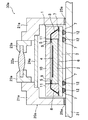
本発明による半導体装置の第1の実施の形態を、図1に示す。
当該固体撮像素子2は、シリコン等からなる半導体基板の一方の主面に、アレイ状に形成された多数の受光素子(フォトセンサ)からなる受光領域4を含み、当該受光素子上にはマイクロレンズ(図示せず)が配設されている。
当該固体撮像素子2は、受光領域4および金バンプ5等が形成された面とは反対側の主面(裏面)が、フィルム状接着剤(ダイス付け材)6によって回路基板3に固定されている。
ここでは、金ボールと金ワイヤとの接続部よりも内側に接着剤を配設した半導体装置を比較例とし、これを、図2(A)に半導体装置1aとして示す。
半導体装置1aは、受光領域4aを有する固体撮像素子2aが、所定の配線パターン7aが形成された回路基板3a上に実装された構成を有している。固体撮像素子2aは、ダイス付け材6aによって回路基板3aに固定されている。
そして、回路基板3aの、固体撮像素子2aの実装側と反対側の面の配線パターン7aには、半田ボール12aが取り付けられている。
図2(A)および図3(A)に示すように、半導体装置1aにあっては、金ワイヤ8aの接続部と受光領域4aとの間に接着剤9aの形成スペースを確保すると共に、固体撮像素子2aのエッジから接着剤9aまでの領域Dに、金ワイヤ8aの接続部が設けられる必要がある。
尚、図4(A),(B)では、ガラス板10a,10、および封止用樹脂11a,11については、図示することを省略している。
従って、当該半導体装置1は、光学特性を損なうことなく、小型・軽量化を実現することができる。
まず、固体撮像素子2複数個と、所定の配線パターン7が形成された大判(大形)の回路基板3を準備し、当該回路基板3上の所定位置に、ダイス付け材6を用いて、複数の固体撮像素子2を固着する(図6参照)。
次いで、前記固体撮像素子2の受光領域4の形成面側に設けられた電極パッド(図示せず)に、金ボール5を配設する(図7参照)。
例えば、電極パッドに所謂ワイヤボンディング法を適用して金線を接続し、これに所定の電流を流して先端部を焼き切り、所定の圧力と熱の条件で超音波を印加し(超音波圧縮)、金ボール5を形成する。その際、金線に流す電流、超音波圧縮時の圧力、熱および超音波を制御することにより、金ボール5のサイズを制御することができる。
次いで、固体撮像素子2に形成した金ボール5と、回路基板3の電極・配線パターン7との間を、金ワイヤ8により接続する(図8参照)。
次いで、一方の主面に選択的に接着剤9が配設されたガラス板10を、個々の固体撮像素子2上に、載置する(図9参照)。
当該ガラス板10には、固体撮像素子2に貼り合わせた際に、金ボール5と金ワイヤ8との接続部に対応する領域に接着剤9を塗布しておき、その塗布面を固体撮像素子2の金ボール5と金ワイヤ8との接続部に貼り合わせる。
何れの場合も、当該接着剤9は、固体撮像素子2の受光領域4を囲繞して配設される。
このとき、ガラス板10の下には、金ボール5と金ワイヤ8との接続部が存在しているため、金型圧力が加わっても、固体撮像素子2とガラス板10の間には、金ボール5と金ワイヤ8との接続部の厚み(高さ)に相当する隙間が確保される。
即ち、前記半導体装置1を電子機器に搭載する際には、前記受光領域4に対し光を効果的に導く為に、当該半導体装置1上には、光学レンズを具備したホルダが配設される。
図16に示すように、ホルダ20は、筐体21に、レンズ22が取り付けられたバレル23が固定された構造を有している。更に当該筐体21内には、IR(赤外線)フィルタ24が固定されている。
例えば、図18に示すように、半導体装置1を、半田ボール12を介してマザーボード31に実装した後、当該半導体装置1を覆い、且つマザーボード31に固定される形態のホルダ20aを用いることも可能である。
このように半導体装置1を覆う形態のホルダ20aを用いる場合には、半導体装置1上に直に搭載するホルダ20を用いた光モジュール30に比べ、光モジュール30aが大型化してしまう。
(第2の実施の形態)
次に、本発明の第2の実施の形態について、図19,図20を用いて説明する。
当該本発明の第2の実施の形態に於ける半導体装置40にあっては、金ワイヤ8等が配設されている部分を封止する封止用樹脂11の上面に、段差部41が設けられている。
当該第2の実施の形態に於ける半導体装置40を用いた光モジュールを図21に示す。
当該半導体装置40を形成する場合も、前記第1の実施の形態に於ける図6乃至図12に示した工程は同様に適用される。
回路基板3の裏面への半田ボール12の取り付け後、所定の刃幅、例えば0.8mm〜1.0mm程度の刃幅を有するブレード60を用い、隣接する固体撮像素子2間(隣接ガラス板10間)の樹脂11に、一方向(X方向)に溝42を形成する(図22参照)。
次いで、ブレード60を用い、隣接する固体撮像素子2間の樹脂11に、前記溝42と直交する方向(Y方向)に溝43を形成する(図23参照)。
次いで、図24,図25に示されるように、前記溝42,43内の中央部(図25中に於ける点線X−X'の位置)に於いてダイシングを行い分割することにより、封止用樹脂11の上面に段差部41が形成された個々の半導体装置40を形成する。尚、図25は、図24のK−K断面を示す。
前記図2a或いは図3aに示す如く、固体撮像素子2aの電極パッド(図示せず)に対し金ワイヤ8aを接続し、当該接続部より内側に接着剤9aを配設する構成にあっては、金ワイヤ8aは通常ファーストボンディングとして接続されるため、樹脂11a内に於いてある程度のループ高さを有する。
そして、当該差部41を用いて、ホルダ20を位置ずれなく配置・固定することができる。
(第3の実施の形態)
次に、本発明の第3の実施の形態について、図27を用いて説明する。
当該本発明の第3の実施の形態に於ける半導体装置70は、金ワイヤ8等が配設されている部分を封止する樹脂11の表面に、ガラス板10側から半導体装置70外側面に向かって傾斜する傾斜部71が配設されている。
このようにして形成される半導体装置の傾斜部71は、レンズを保持するホルダを搭載する際に利用される。
即ち、かかる光モジュールにあっては、半導体装置70に搭載されるホルダ80は、その筐体81の半導体装置70に接着される下端部81aが、当該半導体装置70の傾斜部71の形状・傾斜角に対応した傾斜面とされている。
筐体81の傾斜した端部に接着剤85を塗布し、当該端部を半導体装置70の封止部表面の傾斜部71に接着することにより、図28に示す光モジュール90が構成される。
(第4の実施の形態)
次に、本発明の第4の実施の形態について、図29を用いて説明する。
尚、図29(B)は、平面図(A)に於けるL−L断面を示す。
当該凹状の段差部101は、前記第2の実施の形態と同様に、個片化前の隣接する固体撮像素子2間の封止用樹脂11に、ブレード60を用いて形成する。即ち、X方向、Y方向共に、隣接固体撮像素子2間の封止用樹脂11に平行に2本の溝を形成し、個片化の際には、その平行な2本の溝の間の位置に於いてダイシング処理を行う。
このようにして形成される凹状の段差部101は、レンズを保持するホルダを搭載する際に利用される。
即ち、断面が凹状の段差部101を具備する半導体装置100に搭載されるホルダ110は、その筐体111の半導体装置100に固着される下端部111aが、半導体装置100の凹状の段差部101に対応させた断面凸状とされている。
筐体111の凸状の下端部111aに接着剤115を塗布し、当該先端部を、半導体装置100の凹状の段差部101に嵌合し、接着することにより、図30に示す光モジュール120が構成される。
このように、固体撮像素子2の受光領域4とホルダ110のレンズ112との間の、光軸および距離を考慮した段差部101および筐体111の配設することにより、光軸ずれのない光モジュール120を形成することができる。
(第5の実施の形態)
次に、第5の実施の形態について、図31,図32を用いて説明する。
尚、前記第1の実施の形態で述べた要素と同一の要素については同一の符号を付している。
即ち、当該半導体装置130にあっては、固体撮像素子2の受光領域4の上方に、回路基板3と同等の寸法を有するガラス板131が配置されると共に、固体撮像素子2の外側部に於いて、当該ガラス板131と回路基板3の間に、封止用樹脂11によって封止部が構成されている。
回路基板3上に固体撮像素子を搭載・固着し、当該固体撮像素子の電極端子と回路基板3の配線・電極パターンとをボンディングワイヤにより接続する工程は、前記第1の実施の形態に於いて図6乃至図8に示した工程と同一であるので、詳細な説明は省略する。
次いで、前記接着剤9をその材質に応じた所定の方法により硬化させ、金ボール5と金ワイヤ8との接続部が接着剤9により被覆され、且つガラス基板131が当該接続部により支持された状態をもって、当該固体撮像素子2上に固着された状態とする(図34参照)。
当該封止用樹脂11の注入は、所定の金型を用いての樹脂モールド法が適用される。
このような製造工程により、1枚の回路基板3上に複数個の固体撮像素子2が配置され、当該複数個の固体撮像素子2上に1枚のガラス板131が配設されてなる、個片化前の半導体装置130の集合体が得られる(図37参照)。
上記については単に本発明の原理を示すものである。さらに、多数の変形、変更が当業者にとって可能であり、本発明は上記に示し、説明した正確な構成および応用例に限定されるものではなく、対応するすべての変形例および均等物は、添付の請求項およびその均等物による本発明の範囲とみなされる。
2,2a 半導体チップ
3,3a 回路基板
4,4a 受光領域
5 金属バンプ
6,6a ダイス付け材
7,7a 配線パターン
8,8a 金ワイヤ
9,9a 接着剤
10,10a,131 ガラス板
11,11a 封止用樹脂
12,12a 半田ボール
20,20a,80,110 ホルダ
21,21a,81,111 筐体
21b,81a,111a 下端部
22,22a,82,112 レンズ
23,23a,83,113 バレル
24,24a,84,114 IRフィルタ
25,25a,85,115 接着剤
30,30a,90,120 光モジュール
31 マザーボード
41,41a,101 段差部
71 傾斜部
42,43 溝
60,140 ブレード
Claims (10)
- 電極を有する基板と、
前記基板上に配置され、受光領域と前記受光領域の外側に配設されたバンプとを有する固体撮像素子と、
前記電極と前記バンプとを接続するワイヤ配線と、
前記バンプと前記ワイヤ配線との接続部に配設された接着剤と、
前記受光領域上を覆い且つ前記接続部に支持されて前記接着剤により接着された透明基板と、
前記固体撮像素子の側面および前記ワイヤ配線を封止する封止部と、
を有することを特徴とする半導体装置。 - 前記封止部に、レンズを保持するホルダが固定されていることを特徴とする請求項1記載の半導体装置。
- 電極を有する基板上に、受光領域と前記受光領域の外側に配設されたバンプとを有する固体撮像素子を配置する工程と、
前記電極と前記バンプとをワイヤ配線で接続する工程と、
前記バンプと前記ワイヤ配線との接続部に接着剤を配設し、前記接着剤により、前記固体撮像素子に対向させて透明基板を接着する工程と、
前記固体撮像素子の側面および前記ワイヤ配線を封止する封止部を形成する工程と、
を有することを特徴とする半導体装置の製造方法。 - 前記封止部を形成する工程後に、前記封止部に、レンズを保持するホルダを固定する工程を有することを特徴とする請求項3記載の半導体装置の製造方法。
- 前記封止部を形成する工程後に、前記封止部に、段差部を形成する工程を有することを特徴とする請求項3記載の半導体装置の製造方法。
- 前記段差部を形成する工程後に、前記段差部に、レンズを保持するホルダを固定する工程を有することを特徴とする請求項5記載の半導体装置の製造方法。
- 複数の電極を有する基板上に、各々受光領域と前記受光領域の外側に配設されたバンプとを有する複数の固体撮像素子を配置する工程と、
前記複数の固体撮像素子の前記各バンプと前記基板の前記各電極とをそれぞれワイヤ配線で接続する工程と、
前記バンプと前記ワイヤ配線との各接続部に接着剤を配設し、前記接着剤により、前記複数の固体撮像素子に対向させて透明基板を接着する工程と、
前記複数の固体撮像素子間を封止する封止部を形成する工程と、
前記透明基板、前記封止部および前記基板を切断し、前記固体撮像素子を含む個々の半導体装置に分割する工程と、
を有することを特徴とする半導体装置の製造方法。 - 前記複数の固体撮像素子に対向して前記透明基板を接着する工程においては、
前記複数の固体撮像素子のすべてを覆う1枚の前記透明基板を、前記複数の固体撮像素子のすべてに対向して接着することを特徴とする請求項7記載の半導体装置の製造方法。 - 複数の電極を有する基板上に、各々受光領域と前記受光領域の外側に配設されたバンプとを有する複数の固体撮像素子を配置する工程と、
前記複数の固体撮像素子の前記各バンプと前記基板の前記各電極とをそれぞれワイヤ配線で接続する工程と、
前記バンプと前記ワイヤ配線との各接続部に接着剤を配設し、前記接着剤により、前記複数の固体撮像素子のそれぞれに対向させて複数の透明基板を接着する工程と、
前記複数の固体撮像素子間を封止する封止部を形成する工程と、
前記封止部および前記基板を切断し、前記固体撮像素子を含む個々の半導体装置に分割する工程と、
を有することを特徴とする半導体装置の製造方法。 - 前記封止部を形成する工程後に、前記封止部に溝を形成する工程を有し、
前記溝の形成後、前記溝が形成された前記封止部および前記基板を切断することを特徴とする請求項9記載の半導体装置の製造方法。
Applications Claiming Priority (1)
| Application Number | Priority Date | Filing Date | Title |
|---|---|---|---|
| PCT/JP2006/318400 WO2008032404A1 (fr) | 2006-09-15 | 2006-09-15 | Dispositif à semi-conducteur et son procédé de fabrication |
Publications (2)
| Publication Number | Publication Date |
|---|---|
| JPWO2008032404A1 JPWO2008032404A1 (ja) | 2010-01-21 |
| JP5218058B2 true JP5218058B2 (ja) | 2013-06-26 |
Family
ID=39183475
Family Applications (1)
| Application Number | Title | Priority Date | Filing Date |
|---|---|---|---|
| JP2008534206A Expired - Fee Related JP5218058B2 (ja) | 2006-09-15 | 2006-09-15 | 半導体装置およびその製造方法 |
Country Status (5)
| Country | Link |
|---|---|
| US (1) | US7939361B2 (ja) |
| JP (1) | JP5218058B2 (ja) |
| KR (1) | KR101100790B1 (ja) |
| CN (1) | CN101512765A (ja) |
| WO (1) | WO2008032404A1 (ja) |
Cited By (1)
| Publication number | Priority date | Publication date | Assignee | Title |
|---|---|---|---|---|
| KR20170051972A (ko) * | 2015-11-03 | 2017-05-12 | 삼성전기주식회사 | 이미지 센서 패키지 |
Families Citing this family (49)
| Publication number | Priority date | Publication date | Assignee | Title |
|---|---|---|---|---|
| KR20100058345A (ko) * | 2008-11-24 | 2010-06-03 | 삼성전자주식회사 | 카메라 모듈 형성방법 |
| JP5595066B2 (ja) * | 2009-03-25 | 2014-09-24 | 京セラ株式会社 | 撮像装置および撮像モジュール |
| JP5332834B2 (ja) * | 2009-04-06 | 2013-11-06 | 大日本印刷株式会社 | 撮像素子モジュール |
| KR101640417B1 (ko) | 2010-01-22 | 2016-07-25 | 삼성전자 주식회사 | 반도체 패키지 및 이의 제조 방법 |
| JP5658466B2 (ja) * | 2010-02-05 | 2015-01-28 | キヤノン株式会社 | 固体撮像装置の製造方法 |
| JP2012009816A (ja) * | 2010-05-28 | 2012-01-12 | Casio Comput Co Ltd | 半導体装置およびその製造方法 |
| JP5541088B2 (ja) * | 2010-10-28 | 2014-07-09 | ソニー株式会社 | 撮像素子パッケージ、撮像素子パッケージの製造方法、及び、電子機器 |
| JP2012174800A (ja) * | 2011-02-18 | 2012-09-10 | Sony Corp | 半導体装置、製造装置、及び製造方法 |
| FR2973573A1 (fr) * | 2011-04-01 | 2012-10-05 | St Microelectronics Grenoble 2 | Boitier semi-conducteur comprenant un dispositif semi-conducteur optique |
| JP5746919B2 (ja) * | 2011-06-10 | 2015-07-08 | 新光電気工業株式会社 | 半導体パッケージ |
| JP5634380B2 (ja) | 2011-10-31 | 2014-12-03 | アオイ電子株式会社 | 受光装置およびその製造方法 |
| KR101362348B1 (ko) * | 2012-05-15 | 2014-02-13 | 크루셜텍 (주) | 지문센서 패키지 및 그 제조방법 |
| US8890269B2 (en) * | 2012-05-31 | 2014-11-18 | Stmicroelectronics Pte Ltd. | Optical sensor package with through vias |
| JP6057282B2 (ja) * | 2012-10-04 | 2017-01-11 | セイコーインスツル株式会社 | 光学デバイス及び光学デバイスの製造方法 |
| JP2016027586A (ja) * | 2012-11-29 | 2016-02-18 | パナソニック株式会社 | 光学装置および光学装置の製造方法 |
| EP2884242B1 (en) * | 2013-12-12 | 2021-12-08 | ams International AG | Sensor Package And Manufacturing Method |
| JP6100195B2 (ja) * | 2014-04-09 | 2017-03-22 | 富士フイルム株式会社 | 撮像装置 |
| US9735135B2 (en) * | 2014-12-04 | 2017-08-15 | Pixart Imaging (Penang) Sdn. Bhd. | Optical sensor package and optical sensor assembly |
| US9634059B2 (en) * | 2014-12-30 | 2017-04-25 | Semiconductor Components Industries, Llc | Methods of forming image sensor integrated circuit packages |
| JP2018085353A (ja) | 2015-03-24 | 2018-05-31 | ソニー株式会社 | 固体撮像装置、固体撮像装置の製造方法、及び、電子機器 |
| KR102459731B1 (ko) * | 2015-09-18 | 2022-10-28 | 베이징 지오브이 테크놀로지 컴퍼니 리미티드 | 광학 지문 센서 패키지 |
| KR20170082358A (ko) * | 2016-01-06 | 2017-07-14 | 하나 마이크론(주) | 스마트 기기의 트랙패드 반도체 패키지 및 그 제조 방법 |
| KR102147896B1 (ko) * | 2016-04-28 | 2020-08-25 | 닝보 써니 오포테크 코., 엘티디. | 촬영 모듈 및 그 몰딩 감광 어셈블리, 몰딩 감광 어셈블리의 반제품과 제조 방법 및 전자 기기 |
| EP3267486B1 (en) | 2016-07-06 | 2020-12-30 | Kingpak Technology Inc. | Sensor package structure |
| EP3267485B1 (en) | 2016-07-06 | 2020-11-18 | Kingpak Technology Inc. | Sensor package structure |
| CN107591420B (zh) * | 2016-07-06 | 2020-02-18 | 胜丽国际股份有限公司 | 感测器封装结构 |
| US10692917B2 (en) * | 2016-07-06 | 2020-06-23 | Kingpak Technology Inc. | Sensor package structure |
| WO2018092318A1 (ja) * | 2016-11-21 | 2018-05-24 | オリンパス株式会社 | 内視鏡用撮像モジュール、および内視鏡 |
| CN108401094B (zh) * | 2017-02-08 | 2024-06-11 | 宁波舜宇光电信息有限公司 | 阵列摄像模组及其模塑感光组件和制造方法以及带有阵列摄像模组的电子设备 |
| JP6850661B2 (ja) * | 2017-03-31 | 2021-03-31 | 旭化成エレクトロニクス株式会社 | 光デバイス |
| CN106946215A (zh) * | 2017-04-13 | 2017-07-14 | 华天科技(昆山)电子有限公司 | 带盖板的引线键合型芯片封装结构及其制作方法 |
| US10340250B2 (en) * | 2017-08-15 | 2019-07-02 | Kingpak Technology Inc. | Stack type sensor package structure |
| CN109411487B (zh) * | 2017-08-15 | 2020-09-08 | 胜丽国际股份有限公司 | 堆叠式感测器封装结构 |
| CN108134898B (zh) * | 2018-01-30 | 2020-04-10 | 维沃移动通信有限公司 | 一种摄像头模组、摄像头模组的组装方法及移动终端 |
| JP7368081B2 (ja) * | 2018-10-23 | 2023-10-24 | 旭化成エレクトロニクス株式会社 | 光デバイス |
| WO2020098214A1 (zh) * | 2018-11-12 | 2020-05-22 | 通富微电子股份有限公司 | 一种半导体芯片封装方法及半导体封装器件 |
| WO2020098211A1 (zh) * | 2018-11-12 | 2020-05-22 | 通富微电子股份有限公司 | 一种半导体芯片封装方法及半导体封装器件 |
| KR102716356B1 (ko) * | 2019-01-25 | 2024-10-10 | 삼성전자주식회사 | 생체신호 측정용 텍스쳐 인터페이스 및 이를 포함한 생체신호 측정장치 |
| US11444111B2 (en) * | 2019-03-28 | 2022-09-13 | Semiconductor Components Industries, Llc | Image sensor package having a light blocking member |
| WO2020230404A1 (ja) | 2019-05-15 | 2020-11-19 | ソニーセミコンダクタソリューションズ株式会社 | 半導体パッケージ、半導体パッケージの製造方法、および、電子装置 |
| KR102650997B1 (ko) | 2019-05-20 | 2024-03-25 | 삼성전자주식회사 | 이미지 센서 패키지 |
| CN114651324B (zh) * | 2019-11-14 | 2024-05-07 | 株式会社T-Able | 图像传感器模块以及图像传感器模块的制造方法 |
| EP4071794A4 (en) * | 2019-12-04 | 2023-01-04 | Sony Semiconductor Solutions Corporation | IMAGING DEVICE AND MANUFACTURING METHOD FOR AN IMAGING DEVICE |
| TWI721815B (zh) * | 2020-03-10 | 2021-03-11 | 勝麗國際股份有限公司 | 感測器封裝結構 |
| KR102567061B1 (ko) * | 2020-05-08 | 2023-08-16 | (주)에이피텍 | 와이어 본딩을 이용한 카메라 패키징 장치 |
| US12166050B2 (en) * | 2020-09-20 | 2024-12-10 | UTAC Headquarters Ptd Ltd. | Reliable semiconductor packages |
| TWI762093B (zh) * | 2020-12-18 | 2022-04-21 | 海華科技股份有限公司 | 可攜式電子裝置及其客製化影像擷取模組 |
| TWI769780B (zh) * | 2021-04-12 | 2022-07-01 | 勝麗國際股份有限公司 | 感測器封裝結構 |
| JP2022189647A (ja) * | 2021-06-11 | 2022-12-22 | ソニーセミコンダクタソリューションズ株式会社 | 固体撮像装置および電子機器 |
Citations (7)
| Publication number | Priority date | Publication date | Assignee | Title |
|---|---|---|---|---|
| JPH11354769A (ja) * | 1998-04-10 | 1999-12-24 | Matsushita Electric Ind Co Ltd | 固体撮像装置及びその製造方法 |
| US6342406B1 (en) * | 2000-11-15 | 2002-01-29 | Amkor Technology, Inc. | Flip chip on glass image sensor package fabrication method |
| JP2003163342A (ja) * | 2001-11-29 | 2003-06-06 | Olympus Optical Co Ltd | 固体撮像装置及びその製造方法 |
| JP2005158948A (ja) * | 2003-11-25 | 2005-06-16 | Fuji Photo Film Co Ltd | 固体撮像装置及びその製造方法 |
| JP2005216940A (ja) * | 2004-01-27 | 2005-08-11 | Casio Comput Co Ltd | 光センサモジュール |
| JP2005327893A (ja) * | 2004-05-14 | 2005-11-24 | Matsushita Electric Ind Co Ltd | 光学デバイスおよびその製造方法 |
| JP2006025852A (ja) * | 2004-07-12 | 2006-02-02 | Texas Instr Japan Ltd | 内視鏡用撮像モジュール |
Family Cites Families (5)
| Publication number | Priority date | Publication date | Assignee | Title |
|---|---|---|---|---|
| JP3675402B2 (ja) | 2001-12-27 | 2005-07-27 | セイコーエプソン株式会社 | 光デバイス及びその製造方法、光モジュール、回路基板並びに電子機器 |
| JP4435461B2 (ja) | 2002-03-05 | 2010-03-17 | 富士フイルム株式会社 | 固体撮像装置 |
| TWI296154B (en) * | 2004-01-27 | 2008-04-21 | Casio Computer Co Ltd | Optical sensor module |
| JP2005252183A (ja) | 2004-03-08 | 2005-09-15 | Sony Corp | 固体撮像素子及びその製造方法 |
| JP2006278726A (ja) * | 2005-03-29 | 2006-10-12 | Sharp Corp | 半導体装置モジュール及び半導体装置モジュールの製造方法 |
-
2006
- 2006-09-15 KR KR1020097004725A patent/KR101100790B1/ko active IP Right Grant
- 2006-09-15 WO PCT/JP2006/318400 patent/WO2008032404A1/ja active Application Filing
- 2006-09-15 JP JP2008534206A patent/JP5218058B2/ja not_active Expired - Fee Related
- 2006-09-15 CN CNA2006800557894A patent/CN101512765A/zh active Pending
-
2009
- 2009-03-06 US US12/399,437 patent/US7939361B2/en not_active Expired - Fee Related
Patent Citations (7)
| Publication number | Priority date | Publication date | Assignee | Title |
|---|---|---|---|---|
| JPH11354769A (ja) * | 1998-04-10 | 1999-12-24 | Matsushita Electric Ind Co Ltd | 固体撮像装置及びその製造方法 |
| US6342406B1 (en) * | 2000-11-15 | 2002-01-29 | Amkor Technology, Inc. | Flip chip on glass image sensor package fabrication method |
| JP2003163342A (ja) * | 2001-11-29 | 2003-06-06 | Olympus Optical Co Ltd | 固体撮像装置及びその製造方法 |
| JP2005158948A (ja) * | 2003-11-25 | 2005-06-16 | Fuji Photo Film Co Ltd | 固体撮像装置及びその製造方法 |
| JP2005216940A (ja) * | 2004-01-27 | 2005-08-11 | Casio Comput Co Ltd | 光センサモジュール |
| JP2005327893A (ja) * | 2004-05-14 | 2005-11-24 | Matsushita Electric Ind Co Ltd | 光学デバイスおよびその製造方法 |
| JP2006025852A (ja) * | 2004-07-12 | 2006-02-02 | Texas Instr Japan Ltd | 内視鏡用撮像モジュール |
Cited By (2)
| Publication number | Priority date | Publication date | Assignee | Title |
|---|---|---|---|---|
| KR20170051972A (ko) * | 2015-11-03 | 2017-05-12 | 삼성전기주식회사 | 이미지 센서 패키지 |
| KR102126418B1 (ko) * | 2015-11-03 | 2020-06-24 | 삼성전기주식회사 | 이미지 센서 패키지 |
Also Published As
| Publication number | Publication date |
|---|---|
| KR20090038490A (ko) | 2009-04-20 |
| WO2008032404A1 (fr) | 2008-03-20 |
| CN101512765A (zh) | 2009-08-19 |
| US20090166784A1 (en) | 2009-07-02 |
| JPWO2008032404A1 (ja) | 2010-01-21 |
| KR101100790B1 (ko) | 2012-01-02 |
| US7939361B2 (en) | 2011-05-10 |
Similar Documents
| Publication | Publication Date | Title |
|---|---|---|
| JP5218058B2 (ja) | 半導体装置およびその製造方法 | |
| CN100581216C (zh) | 超小型摄像模块及其制造方法 | |
| JP5934109B2 (ja) | 成形テープフリップチップ画像装置実装を備えたカメラモジュールおよび製造方法 | |
| KR100652375B1 (ko) | 와이어 본딩 패키지를 포함하는 이미지 센서 모듈 구조물및 그 제조방법 | |
| CN100459138C (zh) | 光学器件及其制造方法 | |
| US7759751B2 (en) | Module for optical apparatus and method of producing module for optical apparatus | |
| KR20090128374A (ko) | 고체촬상 장치 및 그 제조 방법 | |
| JP2008092417A (ja) | 半導体撮像素子およびその製造方法並びに半導体撮像装置および半導体撮像モジュール | |
| EP3748948B1 (en) | Camera module, camera module assembly method and mobile terminal | |
| JP2008263550A (ja) | 固体撮像装置およびその製造方法 | |
| US20040256687A1 (en) | Optical module, method of manufacturing the same, and electronic instrument | |
| CN101299432A (zh) | 光学器件及其制造方法 | |
| JP2008193312A (ja) | 撮像装置、その製造方法および携帯端末装置 | |
| JP2005292242A (ja) | 撮像装置および撮像装置の製造方法 | |
| CN113488493B (zh) | 芯片封装结构及其制作方法和模组 | |
| JP4486005B2 (ja) | 半導体撮像装置およびその製造方法 | |
| WO2017134972A1 (ja) | 撮像素子パッケージ及び撮像装置 | |
| JP2009188828A (ja) | 固体撮像装置とその製造方法 | |
| JP2008182051A (ja) | 光学デバイス、光学デバイス装置、カメラモジュールおよび光学デバイス装置の製造方法 | |
| JP2008312104A (ja) | 固体撮像装置およびその製造方法 | |
| KR20120106018A (ko) | 카메라 모듈과, 이의 제조 방법 | |
| JP2008263551A (ja) | 固体撮像装置およびその製造方法 | |
| JP2006005612A (ja) | 撮像モジュール | |
| JP4663667B2 (ja) | 撮像装置、その製造方法および携帯端末装置 | |
| JP2006294720A (ja) | カメラモジュール |
Legal Events
| Date | Code | Title | Description |
|---|---|---|---|
| A131 | Notification of reasons for refusal |
Free format text: JAPANESE INTERMEDIATE CODE: A131 Effective date: 20120515 |
|
| A521 | Request for written amendment filed |
Free format text: JAPANESE INTERMEDIATE CODE: A523 Effective date: 20120711 |
|
| TRDD | Decision of grant or rejection written | ||
| A01 | Written decision to grant a patent or to grant a registration (utility model) |
Free format text: JAPANESE INTERMEDIATE CODE: A01 Effective date: 20130205 |
|
| A61 | First payment of annual fees (during grant procedure) |
Free format text: JAPANESE INTERMEDIATE CODE: A61 Effective date: 20130218 |
|
| FPAY | Renewal fee payment (event date is renewal date of database) |
Free format text: PAYMENT UNTIL: 20160315 Year of fee payment: 3 |
|
| R150 | Certificate of patent or registration of utility model |
Ref document number: 5218058 Country of ref document: JP Free format text: JAPANESE INTERMEDIATE CODE: R150 Free format text: JAPANESE INTERMEDIATE CODE: R150 |
|
| S111 | Request for change of ownership or part of ownership |
Free format text: JAPANESE INTERMEDIATE CODE: R313111 |
|
| R350 | Written notification of registration of transfer |
Free format text: JAPANESE INTERMEDIATE CODE: R350 |
|
| LAPS | Cancellation because of no payment of annual fees |