JP5149881B2 - 半導体装置の製造方法 - Google Patents
半導体装置の製造方法 Download PDFInfo
- Publication number
- JP5149881B2 JP5149881B2 JP2009226679A JP2009226679A JP5149881B2 JP 5149881 B2 JP5149881 B2 JP 5149881B2 JP 2009226679 A JP2009226679 A JP 2009226679A JP 2009226679 A JP2009226679 A JP 2009226679A JP 5149881 B2 JP5149881 B2 JP 5149881B2
- Authority
- JP
- Japan
- Prior art keywords
- substrate
- sub
- main surface
- hole
- base
- Prior art date
- Legal status (The legal status is an assumption and is not a legal conclusion. Google has not performed a legal analysis and makes no representation as to the accuracy of the status listed.)
- Expired - Fee Related
Links
- 239000004065 semiconductor Substances 0.000 title claims abstract description 117
- 238000004519 manufacturing process Methods 0.000 title claims description 36
- 238000007789 sealing Methods 0.000 claims abstract description 178
- 229920005989 resin Polymers 0.000 claims abstract description 99
- 239000011347 resin Substances 0.000 claims abstract description 99
- 239000000463 material Substances 0.000 claims description 114
- 238000000034 method Methods 0.000 claims description 82
- 239000000758 substrate Substances 0.000 abstract description 435
- 229910000679 solder Inorganic materials 0.000 abstract description 72
- 230000008878 coupling Effects 0.000 abstract 1
- 238000010168 coupling process Methods 0.000 abstract 1
- 238000005859 coupling reaction Methods 0.000 abstract 1
- 230000008569 process Effects 0.000 description 57
- 230000004048 modification Effects 0.000 description 50
- 238000012986 modification Methods 0.000 description 50
- 230000015572 biosynthetic process Effects 0.000 description 33
- 238000000465 moulding Methods 0.000 description 32
- 239000010410 layer Substances 0.000 description 28
- 238000002360 preparation method Methods 0.000 description 12
- 239000010949 copper Substances 0.000 description 7
- 238000002844 melting Methods 0.000 description 7
- 230000008018 melting Effects 0.000 description 7
- 238000007747 plating Methods 0.000 description 7
- 101150025129 POP1 gene Proteins 0.000 description 6
- 238000004140 cleaning Methods 0.000 description 5
- PXHVJJICTQNCMI-UHFFFAOYSA-N Nickel Chemical compound [Ni] PXHVJJICTQNCMI-UHFFFAOYSA-N 0.000 description 4
- 230000000694 effects Effects 0.000 description 4
- 239000010931 gold Substances 0.000 description 4
- 238000010438 heat treatment Methods 0.000 description 4
- 230000001678 irradiating effect Effects 0.000 description 4
- 230000000149 penetrating effect Effects 0.000 description 4
- ATJFFYVFTNAWJD-UHFFFAOYSA-N Tin Chemical compound [Sn] ATJFFYVFTNAWJD-UHFFFAOYSA-N 0.000 description 3
- 238000001723 curing Methods 0.000 description 3
- 238000005516 engineering process Methods 0.000 description 3
- 239000003822 epoxy resin Substances 0.000 description 3
- 239000011521 glass Substances 0.000 description 3
- PCHJSUWPFVWCPO-UHFFFAOYSA-N gold Chemical compound [Au] PCHJSUWPFVWCPO-UHFFFAOYSA-N 0.000 description 3
- 229910052737 gold Inorganic materials 0.000 description 3
- 239000011159 matrix material Substances 0.000 description 3
- 239000007769 metal material Substances 0.000 description 3
- 230000002093 peripheral effect Effects 0.000 description 3
- 229920000647 polyepoxide Polymers 0.000 description 3
- 229910052710 silicon Inorganic materials 0.000 description 3
- 239000010703 silicon Substances 0.000 description 3
- 239000002356 single layer Substances 0.000 description 3
- RYGMFSIKBFXOCR-UHFFFAOYSA-N Copper Chemical compound [Cu] RYGMFSIKBFXOCR-UHFFFAOYSA-N 0.000 description 2
- 229910000577 Silicon-germanium Inorganic materials 0.000 description 2
- 239000000853 adhesive Substances 0.000 description 2
- 230000001070 adhesive effect Effects 0.000 description 2
- 229910045601 alloy Inorganic materials 0.000 description 2
- 239000000956 alloy Substances 0.000 description 2
- 239000000919 ceramic Substances 0.000 description 2
- 229910052802 copper Inorganic materials 0.000 description 2
- 238000007689 inspection Methods 0.000 description 2
- 239000002923 metal particle Substances 0.000 description 2
- 229910052759 nickel Inorganic materials 0.000 description 2
- 238000004904 shortening Methods 0.000 description 2
- 239000007787 solid Substances 0.000 description 2
- 230000008961 swelling Effects 0.000 description 2
- 102100035475 Blood vessel epicardial substance Human genes 0.000 description 1
- 229920000049 Carbon (fiber) Polymers 0.000 description 1
- 101001094636 Homo sapiens Blood vessel epicardial substance Proteins 0.000 description 1
- 101000608194 Homo sapiens Pyrin domain-containing protein 1 Proteins 0.000 description 1
- 101000595404 Homo sapiens Ribonucleases P/MRP protein subunit POP1 Proteins 0.000 description 1
- LEVVHYCKPQWKOP-UHFFFAOYSA-N [Si].[Ge] Chemical compound [Si].[Ge] LEVVHYCKPQWKOP-UHFFFAOYSA-N 0.000 description 1
- 239000000654 additive Substances 0.000 description 1
- 230000008901 benefit Effects 0.000 description 1
- 229910052797 bismuth Inorganic materials 0.000 description 1
- JCXGWMGPZLAOME-UHFFFAOYSA-N bismuth atom Chemical compound [Bi] JCXGWMGPZLAOME-UHFFFAOYSA-N 0.000 description 1
- 239000003990 capacitor Substances 0.000 description 1
- 239000004917 carbon fiber Substances 0.000 description 1
- 239000004020 conductor Substances 0.000 description 1
- 238000011109 contamination Methods 0.000 description 1
- 230000008602 contraction Effects 0.000 description 1
- 239000006071 cream Substances 0.000 description 1
- 238000005520 cutting process Methods 0.000 description 1
- 230000002950 deficient Effects 0.000 description 1
- 235000012489 doughnuts Nutrition 0.000 description 1
- 238000005530 etching Methods 0.000 description 1
- 239000003365 glass fiber Substances 0.000 description 1
- 239000000383 hazardous chemical Substances 0.000 description 1
- 238000013007 heat curing Methods 0.000 description 1
- 239000011810 insulating material Substances 0.000 description 1
- VNWKTOKETHGBQD-UHFFFAOYSA-N methane Chemical compound C VNWKTOKETHGBQD-UHFFFAOYSA-N 0.000 description 1
- 239000000203 mixture Substances 0.000 description 1
- 238000010943 off-gassing Methods 0.000 description 1
- 239000002957 persistent organic pollutant Substances 0.000 description 1
- 230000000704 physical effect Effects 0.000 description 1
- 229920001721 polyimide Polymers 0.000 description 1
- 239000009719 polyimide resin Substances 0.000 description 1
- 238000003672 processing method Methods 0.000 description 1
- 230000009467 reduction Effects 0.000 description 1
- 238000007493 shaping process Methods 0.000 description 1
- 229910052709 silver Inorganic materials 0.000 description 1
- 239000004332 silver Substances 0.000 description 1
- 229920001187 thermosetting polymer Polymers 0.000 description 1
Images


Classifications
-
- H—ELECTRICITY
- H01—ELECTRIC ELEMENTS
- H01L—SEMICONDUCTOR DEVICES NOT COVERED BY CLASS H10
- H01L25/00—Assemblies consisting of a plurality of semiconductor or other solid state devices
- H01L25/50—Multistep manufacturing processes of assemblies consisting of devices, the devices being individual devices of subclass H10D or integrated devices of class H10
-
- H—ELECTRICITY
- H01—ELECTRIC ELEMENTS
- H01L—SEMICONDUCTOR DEVICES NOT COVERED BY CLASS H10
- H01L21/00—Processes or apparatus adapted for the manufacture or treatment of semiconductor or solid state devices or of parts thereof
- H01L21/02—Manufacture or treatment of semiconductor devices or of parts thereof
- H01L21/04—Manufacture or treatment of semiconductor devices or of parts thereof the devices having potential barriers, e.g. a PN junction, depletion layer or carrier concentration layer
- H01L21/50—Assembly of semiconductor devices using processes or apparatus not provided for in a single one of the groups H01L21/18 - H01L21/326 or H10D48/04 - H10D48/07 e.g. sealing of a cap to a base of a container
- H01L21/56—Encapsulations, e.g. encapsulation layers, coatings
- H01L21/561—Batch processing
-
- H—ELECTRICITY
- H01—ELECTRIC ELEMENTS
- H01L—SEMICONDUCTOR DEVICES NOT COVERED BY CLASS H10
- H01L21/00—Processes or apparatus adapted for the manufacture or treatment of semiconductor or solid state devices or of parts thereof
- H01L21/02—Manufacture or treatment of semiconductor devices or of parts thereof
- H01L21/04—Manufacture or treatment of semiconductor devices or of parts thereof the devices having potential barriers, e.g. a PN junction, depletion layer or carrier concentration layer
- H01L21/50—Assembly of semiconductor devices using processes or apparatus not provided for in a single one of the groups H01L21/18 - H01L21/326 or H10D48/04 - H10D48/07 e.g. sealing of a cap to a base of a container
- H01L21/56—Encapsulations, e.g. encapsulation layers, coatings
- H01L21/565—Moulds
-
- H—ELECTRICITY
- H01—ELECTRIC ELEMENTS
- H01L—SEMICONDUCTOR DEVICES NOT COVERED BY CLASS H10
- H01L23/00—Details of semiconductor or other solid state devices
- H01L23/28—Encapsulations, e.g. encapsulating layers, coatings, e.g. for protection
- H01L23/31—Encapsulations, e.g. encapsulating layers, coatings, e.g. for protection characterised by the arrangement or shape
- H01L23/3107—Encapsulations, e.g. encapsulating layers, coatings, e.g. for protection characterised by the arrangement or shape the device being completely enclosed
- H01L23/3121—Encapsulations, e.g. encapsulating layers, coatings, e.g. for protection characterised by the arrangement or shape the device being completely enclosed a substrate forming part of the encapsulation
- H01L23/3128—Encapsulations, e.g. encapsulating layers, coatings, e.g. for protection characterised by the arrangement or shape the device being completely enclosed a substrate forming part of the encapsulation the substrate having spherical bumps for external connection
-
- H—ELECTRICITY
- H01—ELECTRIC ELEMENTS
- H01L—SEMICONDUCTOR DEVICES NOT COVERED BY CLASS H10
- H01L23/00—Details of semiconductor or other solid state devices
- H01L23/48—Arrangements for conducting electric current to or from the solid state body in operation, e.g. leads, terminal arrangements ; Selection of materials therefor
- H01L23/488—Arrangements for conducting electric current to or from the solid state body in operation, e.g. leads, terminal arrangements ; Selection of materials therefor consisting of soldered or bonded constructions
- H01L23/498—Leads, i.e. metallisations or lead-frames on insulating substrates, e.g. chip carriers
- H01L23/49833—Leads, i.e. metallisations or lead-frames on insulating substrates, e.g. chip carriers the chip support structure consisting of a plurality of insulating substrates
-
- H—ELECTRICITY
- H01—ELECTRIC ELEMENTS
- H01L—SEMICONDUCTOR DEVICES NOT COVERED BY CLASS H10
- H01L24/00—Arrangements for connecting or disconnecting semiconductor or solid-state bodies; Methods or apparatus related thereto
- H01L24/93—Batch processes
- H01L24/95—Batch processes at chip-level, i.e. with connecting carried out on a plurality of singulated devices, i.e. on diced chips
- H01L24/97—Batch processes at chip-level, i.e. with connecting carried out on a plurality of singulated devices, i.e. on diced chips the devices being connected to a common substrate, e.g. interposer, said common substrate being separable into individual assemblies after connecting
-
- H—ELECTRICITY
- H01—ELECTRIC ELEMENTS
- H01L—SEMICONDUCTOR DEVICES NOT COVERED BY CLASS H10
- H01L25/00—Assemblies consisting of a plurality of semiconductor or other solid state devices
- H01L25/03—Assemblies consisting of a plurality of semiconductor or other solid state devices all the devices being of a type provided for in a single subclass of subclasses H10B, H10F, H10H, H10K or H10N, e.g. assemblies of rectifier diodes
- H01L25/04—Assemblies consisting of a plurality of semiconductor or other solid state devices all the devices being of a type provided for in a single subclass of subclasses H10B, H10F, H10H, H10K or H10N, e.g. assemblies of rectifier diodes the devices not having separate containers
- H01L25/065—Assemblies consisting of a plurality of semiconductor or other solid state devices all the devices being of a type provided for in a single subclass of subclasses H10B, H10F, H10H, H10K or H10N, e.g. assemblies of rectifier diodes the devices not having separate containers the devices being of a type provided for in group H10D89/00
- H01L25/0652—Assemblies consisting of a plurality of semiconductor or other solid state devices all the devices being of a type provided for in a single subclass of subclasses H10B, H10F, H10H, H10K or H10N, e.g. assemblies of rectifier diodes the devices not having separate containers the devices being of a type provided for in group H10D89/00 the devices being arranged next and on each other, i.e. mixed assemblies
-
- H—ELECTRICITY
- H01—ELECTRIC ELEMENTS
- H01L—SEMICONDUCTOR DEVICES NOT COVERED BY CLASS H10
- H01L25/00—Assemblies consisting of a plurality of semiconductor or other solid state devices
- H01L25/16—Assemblies consisting of a plurality of semiconductor or other solid state devices the devices being of types provided for in two or more different subclasses of H10B, H10D, H10F, H10H, H10K or H10N, e.g. forming hybrid circuits
-
- H—ELECTRICITY
- H01—ELECTRIC ELEMENTS
- H01L—SEMICONDUCTOR DEVICES NOT COVERED BY CLASS H10
- H01L2224/00—Indexing scheme for arrangements for connecting or disconnecting semiconductor or solid-state bodies and methods related thereto as covered by H01L24/00
- H01L2224/01—Means for bonding being attached to, or being formed on, the surface to be connected, e.g. chip-to-package, die-attach, "first-level" interconnects; Manufacturing methods related thereto
- H01L2224/02—Bonding areas; Manufacturing methods related thereto
- H01L2224/04—Structure, shape, material or disposition of the bonding areas prior to the connecting process
- H01L2224/05—Structure, shape, material or disposition of the bonding areas prior to the connecting process of an individual bonding area
- H01L2224/0554—External layer
- H01L2224/0555—Shape
- H01L2224/05552—Shape in top view
- H01L2224/05553—Shape in top view being rectangular
-
- H—ELECTRICITY
- H01—ELECTRIC ELEMENTS
- H01L—SEMICONDUCTOR DEVICES NOT COVERED BY CLASS H10
- H01L2224/00—Indexing scheme for arrangements for connecting or disconnecting semiconductor or solid-state bodies and methods related thereto as covered by H01L24/00
- H01L2224/01—Means for bonding being attached to, or being formed on, the surface to be connected, e.g. chip-to-package, die-attach, "first-level" interconnects; Manufacturing methods related thereto
- H01L2224/26—Layer connectors, e.g. plate connectors, solder or adhesive layers; Manufacturing methods related thereto
- H01L2224/31—Structure, shape, material or disposition of the layer connectors after the connecting process
- H01L2224/32—Structure, shape, material or disposition of the layer connectors after the connecting process of an individual layer connector
- H01L2224/321—Disposition
- H01L2224/32151—Disposition the layer connector connecting between a semiconductor or solid-state body and an item not being a semiconductor or solid-state body, e.g. chip-to-substrate, chip-to-passive
- H01L2224/32221—Disposition the layer connector connecting between a semiconductor or solid-state body and an item not being a semiconductor or solid-state body, e.g. chip-to-substrate, chip-to-passive the body and the item being stacked
- H01L2224/32225—Disposition the layer connector connecting between a semiconductor or solid-state body and an item not being a semiconductor or solid-state body, e.g. chip-to-substrate, chip-to-passive the body and the item being stacked the item being non-metallic, e.g. insulating substrate with or without metallisation
-
- H—ELECTRICITY
- H01—ELECTRIC ELEMENTS
- H01L—SEMICONDUCTOR DEVICES NOT COVERED BY CLASS H10
- H01L2224/00—Indexing scheme for arrangements for connecting or disconnecting semiconductor or solid-state bodies and methods related thereto as covered by H01L24/00
- H01L2224/01—Means for bonding being attached to, or being formed on, the surface to be connected, e.g. chip-to-package, die-attach, "first-level" interconnects; Manufacturing methods related thereto
- H01L2224/42—Wire connectors; Manufacturing methods related thereto
- H01L2224/44—Structure, shape, material or disposition of the wire connectors prior to the connecting process
- H01L2224/45—Structure, shape, material or disposition of the wire connectors prior to the connecting process of an individual wire connector
- H01L2224/45001—Core members of the connector
- H01L2224/45099—Material
- H01L2224/451—Material with a principal constituent of the material being a metal or a metalloid, e.g. boron (B), silicon (Si), germanium (Ge), arsenic (As), antimony (Sb), tellurium (Te) and polonium (Po), and alloys thereof
- H01L2224/45138—Material with a principal constituent of the material being a metal or a metalloid, e.g. boron (B), silicon (Si), germanium (Ge), arsenic (As), antimony (Sb), tellurium (Te) and polonium (Po), and alloys thereof the principal constituent melting at a temperature of greater than or equal to 950°C and less than 1550°C
- H01L2224/45144—Gold (Au) as principal constituent
-
- H—ELECTRICITY
- H01—ELECTRIC ELEMENTS
- H01L—SEMICONDUCTOR DEVICES NOT COVERED BY CLASS H10
- H01L2224/00—Indexing scheme for arrangements for connecting or disconnecting semiconductor or solid-state bodies and methods related thereto as covered by H01L24/00
- H01L2224/01—Means for bonding being attached to, or being formed on, the surface to be connected, e.g. chip-to-package, die-attach, "first-level" interconnects; Manufacturing methods related thereto
- H01L2224/42—Wire connectors; Manufacturing methods related thereto
- H01L2224/47—Structure, shape, material or disposition of the wire connectors after the connecting process
- H01L2224/48—Structure, shape, material or disposition of the wire connectors after the connecting process of an individual wire connector
- H01L2224/4805—Shape
- H01L2224/4809—Loop shape
- H01L2224/48091—Arched
-
- H—ELECTRICITY
- H01—ELECTRIC ELEMENTS
- H01L—SEMICONDUCTOR DEVICES NOT COVERED BY CLASS H10
- H01L2224/00—Indexing scheme for arrangements for connecting or disconnecting semiconductor or solid-state bodies and methods related thereto as covered by H01L24/00
- H01L2224/01—Means for bonding being attached to, or being formed on, the surface to be connected, e.g. chip-to-package, die-attach, "first-level" interconnects; Manufacturing methods related thereto
- H01L2224/42—Wire connectors; Manufacturing methods related thereto
- H01L2224/47—Structure, shape, material or disposition of the wire connectors after the connecting process
- H01L2224/48—Structure, shape, material or disposition of the wire connectors after the connecting process of an individual wire connector
- H01L2224/481—Disposition
- H01L2224/48151—Connecting between a semiconductor or solid-state body and an item not being a semiconductor or solid-state body, e.g. chip-to-substrate, chip-to-passive
- H01L2224/48221—Connecting between a semiconductor or solid-state body and an item not being a semiconductor or solid-state body, e.g. chip-to-substrate, chip-to-passive the body and the item being stacked
- H01L2224/48225—Connecting between a semiconductor or solid-state body and an item not being a semiconductor or solid-state body, e.g. chip-to-substrate, chip-to-passive the body and the item being stacked the item being non-metallic, e.g. insulating substrate with or without metallisation
- H01L2224/48227—Connecting between a semiconductor or solid-state body and an item not being a semiconductor or solid-state body, e.g. chip-to-substrate, chip-to-passive the body and the item being stacked the item being non-metallic, e.g. insulating substrate with or without metallisation connecting the wire to a bond pad of the item
-
- H—ELECTRICITY
- H01—ELECTRIC ELEMENTS
- H01L—SEMICONDUCTOR DEVICES NOT COVERED BY CLASS H10
- H01L2224/00—Indexing scheme for arrangements for connecting or disconnecting semiconductor or solid-state bodies and methods related thereto as covered by H01L24/00
- H01L2224/01—Means for bonding being attached to, or being formed on, the surface to be connected, e.g. chip-to-package, die-attach, "first-level" interconnects; Manufacturing methods related thereto
- H01L2224/42—Wire connectors; Manufacturing methods related thereto
- H01L2224/47—Structure, shape, material or disposition of the wire connectors after the connecting process
- H01L2224/48—Structure, shape, material or disposition of the wire connectors after the connecting process of an individual wire connector
- H01L2224/484—Connecting portions
- H01L2224/48463—Connecting portions the connecting portion on the bonding area of the semiconductor or solid-state body being a ball bond
- H01L2224/48465—Connecting portions the connecting portion on the bonding area of the semiconductor or solid-state body being a ball bond the other connecting portion not on the bonding area being a wedge bond, i.e. ball-to-wedge, regular stitch
-
- H—ELECTRICITY
- H01—ELECTRIC ELEMENTS
- H01L—SEMICONDUCTOR DEVICES NOT COVERED BY CLASS H10
- H01L2224/00—Indexing scheme for arrangements for connecting or disconnecting semiconductor or solid-state bodies and methods related thereto as covered by H01L24/00
- H01L2224/01—Means for bonding being attached to, or being formed on, the surface to be connected, e.g. chip-to-package, die-attach, "first-level" interconnects; Manufacturing methods related thereto
- H01L2224/42—Wire connectors; Manufacturing methods related thereto
- H01L2224/47—Structure, shape, material or disposition of the wire connectors after the connecting process
- H01L2224/49—Structure, shape, material or disposition of the wire connectors after the connecting process of a plurality of wire connectors
- H01L2224/491—Disposition
- H01L2224/4912—Layout
- H01L2224/49171—Fan-out arrangements
-
- H—ELECTRICITY
- H01—ELECTRIC ELEMENTS
- H01L—SEMICONDUCTOR DEVICES NOT COVERED BY CLASS H10
- H01L2224/00—Indexing scheme for arrangements for connecting or disconnecting semiconductor or solid-state bodies and methods related thereto as covered by H01L24/00
- H01L2224/73—Means for bonding being of different types provided for in two or more of groups H01L2224/10, H01L2224/18, H01L2224/26, H01L2224/34, H01L2224/42, H01L2224/50, H01L2224/63, H01L2224/71
- H01L2224/732—Location after the connecting process
- H01L2224/73251—Location after the connecting process on different surfaces
- H01L2224/73265—Layer and wire connectors
-
- H—ELECTRICITY
- H01—ELECTRIC ELEMENTS
- H01L—SEMICONDUCTOR DEVICES NOT COVERED BY CLASS H10
- H01L2224/00—Indexing scheme for arrangements for connecting or disconnecting semiconductor or solid-state bodies and methods related thereto as covered by H01L24/00
- H01L2224/93—Batch processes
- H01L2224/95—Batch processes at chip-level, i.e. with connecting carried out on a plurality of singulated devices, i.e. on diced chips
- H01L2224/97—Batch processes at chip-level, i.e. with connecting carried out on a plurality of singulated devices, i.e. on diced chips the devices being connected to a common substrate, e.g. interposer, said common substrate being separable into individual assemblies after connecting
-
- H—ELECTRICITY
- H01—ELECTRIC ELEMENTS
- H01L—SEMICONDUCTOR DEVICES NOT COVERED BY CLASS H10
- H01L23/00—Details of semiconductor or other solid state devices
- H01L23/48—Arrangements for conducting electric current to or from the solid state body in operation, e.g. leads, terminal arrangements ; Selection of materials therefor
- H01L23/488—Arrangements for conducting electric current to or from the solid state body in operation, e.g. leads, terminal arrangements ; Selection of materials therefor consisting of soldered or bonded constructions
- H01L23/498—Leads, i.e. metallisations or lead-frames on insulating substrates, e.g. chip carriers
- H01L23/49811—Additional leads joined to the metallisation on the insulating substrate, e.g. pins, bumps, wires, flat leads
- H01L23/49816—Spherical bumps on the substrate for external connection, e.g. ball grid arrays [BGA]
-
- H—ELECTRICITY
- H01—ELECTRIC ELEMENTS
- H01L—SEMICONDUCTOR DEVICES NOT COVERED BY CLASS H10
- H01L24/00—Arrangements for connecting or disconnecting semiconductor or solid-state bodies; Methods or apparatus related thereto
- H01L24/01—Means for bonding being attached to, or being formed on, the surface to be connected, e.g. chip-to-package, die-attach, "first-level" interconnects; Manufacturing methods related thereto
- H01L24/42—Wire connectors; Manufacturing methods related thereto
- H01L24/44—Structure, shape, material or disposition of the wire connectors prior to the connecting process
- H01L24/45—Structure, shape, material or disposition of the wire connectors prior to the connecting process of an individual wire connector
-
- H—ELECTRICITY
- H01—ELECTRIC ELEMENTS
- H01L—SEMICONDUCTOR DEVICES NOT COVERED BY CLASS H10
- H01L24/00—Arrangements for connecting or disconnecting semiconductor or solid-state bodies; Methods or apparatus related thereto
- H01L24/01—Means for bonding being attached to, or being formed on, the surface to be connected, e.g. chip-to-package, die-attach, "first-level" interconnects; Manufacturing methods related thereto
- H01L24/42—Wire connectors; Manufacturing methods related thereto
- H01L24/47—Structure, shape, material or disposition of the wire connectors after the connecting process
- H01L24/48—Structure, shape, material or disposition of the wire connectors after the connecting process of an individual wire connector
-
- H—ELECTRICITY
- H01—ELECTRIC ELEMENTS
- H01L—SEMICONDUCTOR DEVICES NOT COVERED BY CLASS H10
- H01L24/00—Arrangements for connecting or disconnecting semiconductor or solid-state bodies; Methods or apparatus related thereto
- H01L24/01—Means for bonding being attached to, or being formed on, the surface to be connected, e.g. chip-to-package, die-attach, "first-level" interconnects; Manufacturing methods related thereto
- H01L24/42—Wire connectors; Manufacturing methods related thereto
- H01L24/47—Structure, shape, material or disposition of the wire connectors after the connecting process
- H01L24/49—Structure, shape, material or disposition of the wire connectors after the connecting process of a plurality of wire connectors
-
- H—ELECTRICITY
- H01—ELECTRIC ELEMENTS
- H01L—SEMICONDUCTOR DEVICES NOT COVERED BY CLASS H10
- H01L24/00—Arrangements for connecting or disconnecting semiconductor or solid-state bodies; Methods or apparatus related thereto
- H01L24/73—Means for bonding being of different types provided for in two or more of groups H01L24/10, H01L24/18, H01L24/26, H01L24/34, H01L24/42, H01L24/50, H01L24/63, H01L24/71
-
- H—ELECTRICITY
- H01—ELECTRIC ELEMENTS
- H01L—SEMICONDUCTOR DEVICES NOT COVERED BY CLASS H10
- H01L2924/00—Indexing scheme for arrangements or methods for connecting or disconnecting semiconductor or solid-state bodies as covered by H01L24/00
- H01L2924/01—Chemical elements
- H01L2924/01005—Boron [B]
-
- H—ELECTRICITY
- H01—ELECTRIC ELEMENTS
- H01L—SEMICONDUCTOR DEVICES NOT COVERED BY CLASS H10
- H01L2924/00—Indexing scheme for arrangements or methods for connecting or disconnecting semiconductor or solid-state bodies as covered by H01L24/00
- H01L2924/01—Chemical elements
- H01L2924/01006—Carbon [C]
-
- H—ELECTRICITY
- H01—ELECTRIC ELEMENTS
- H01L—SEMICONDUCTOR DEVICES NOT COVERED BY CLASS H10
- H01L2924/00—Indexing scheme for arrangements or methods for connecting or disconnecting semiconductor or solid-state bodies as covered by H01L24/00
- H01L2924/01—Chemical elements
- H01L2924/01014—Silicon [Si]
-
- H—ELECTRICITY
- H01—ELECTRIC ELEMENTS
- H01L—SEMICONDUCTOR DEVICES NOT COVERED BY CLASS H10
- H01L2924/00—Indexing scheme for arrangements or methods for connecting or disconnecting semiconductor or solid-state bodies as covered by H01L24/00
- H01L2924/01—Chemical elements
- H01L2924/01028—Nickel [Ni]
-
- H—ELECTRICITY
- H01—ELECTRIC ELEMENTS
- H01L—SEMICONDUCTOR DEVICES NOT COVERED BY CLASS H10
- H01L2924/00—Indexing scheme for arrangements or methods for connecting or disconnecting semiconductor or solid-state bodies as covered by H01L24/00
- H01L2924/01—Chemical elements
- H01L2924/01029—Copper [Cu]
-
- H—ELECTRICITY
- H01—ELECTRIC ELEMENTS
- H01L—SEMICONDUCTOR DEVICES NOT COVERED BY CLASS H10
- H01L2924/00—Indexing scheme for arrangements or methods for connecting or disconnecting semiconductor or solid-state bodies as covered by H01L24/00
- H01L2924/01—Chemical elements
- H01L2924/01033—Arsenic [As]
-
- H—ELECTRICITY
- H01—ELECTRIC ELEMENTS
- H01L—SEMICONDUCTOR DEVICES NOT COVERED BY CLASS H10
- H01L2924/00—Indexing scheme for arrangements or methods for connecting or disconnecting semiconductor or solid-state bodies as covered by H01L24/00
- H01L2924/01—Chemical elements
- H01L2924/01047—Silver [Ag]
-
- H—ELECTRICITY
- H01—ELECTRIC ELEMENTS
- H01L—SEMICONDUCTOR DEVICES NOT COVERED BY CLASS H10
- H01L2924/00—Indexing scheme for arrangements or methods for connecting or disconnecting semiconductor or solid-state bodies as covered by H01L24/00
- H01L2924/01—Chemical elements
- H01L2924/0105—Tin [Sn]
-
- H—ELECTRICITY
- H01—ELECTRIC ELEMENTS
- H01L—SEMICONDUCTOR DEVICES NOT COVERED BY CLASS H10
- H01L2924/00—Indexing scheme for arrangements or methods for connecting or disconnecting semiconductor or solid-state bodies as covered by H01L24/00
- H01L2924/01—Chemical elements
- H01L2924/01075—Rhenium [Re]
-
- H—ELECTRICITY
- H01—ELECTRIC ELEMENTS
- H01L—SEMICONDUCTOR DEVICES NOT COVERED BY CLASS H10
- H01L2924/00—Indexing scheme for arrangements or methods for connecting or disconnecting semiconductor or solid-state bodies as covered by H01L24/00
- H01L2924/01—Chemical elements
- H01L2924/01078—Platinum [Pt]
-
- H—ELECTRICITY
- H01—ELECTRIC ELEMENTS
- H01L—SEMICONDUCTOR DEVICES NOT COVERED BY CLASS H10
- H01L2924/00—Indexing scheme for arrangements or methods for connecting or disconnecting semiconductor or solid-state bodies as covered by H01L24/00
- H01L2924/01—Chemical elements
- H01L2924/01079—Gold [Au]
-
- H—ELECTRICITY
- H01—ELECTRIC ELEMENTS
- H01L—SEMICONDUCTOR DEVICES NOT COVERED BY CLASS H10
- H01L2924/00—Indexing scheme for arrangements or methods for connecting or disconnecting semiconductor or solid-state bodies as covered by H01L24/00
- H01L2924/01—Chemical elements
- H01L2924/01082—Lead [Pb]
-
- H—ELECTRICITY
- H01—ELECTRIC ELEMENTS
- H01L—SEMICONDUCTOR DEVICES NOT COVERED BY CLASS H10
- H01L2924/00—Indexing scheme for arrangements or methods for connecting or disconnecting semiconductor or solid-state bodies as covered by H01L24/00
- H01L2924/013—Alloys
- H01L2924/014—Solder alloys
-
- H—ELECTRICITY
- H01—ELECTRIC ELEMENTS
- H01L—SEMICONDUCTOR DEVICES NOT COVERED BY CLASS H10
- H01L2924/00—Indexing scheme for arrangements or methods for connecting or disconnecting semiconductor or solid-state bodies as covered by H01L24/00
- H01L2924/10—Details of semiconductor or other solid state devices to be connected
- H01L2924/11—Device type
- H01L2924/14—Integrated circuits
-
- H—ELECTRICITY
- H01—ELECTRIC ELEMENTS
- H01L—SEMICONDUCTOR DEVICES NOT COVERED BY CLASS H10
- H01L2924/00—Indexing scheme for arrangements or methods for connecting or disconnecting semiconductor or solid-state bodies as covered by H01L24/00
- H01L2924/15—Details of package parts other than the semiconductor or other solid state devices to be connected
- H01L2924/151—Die mounting substrate
- H01L2924/1517—Multilayer substrate
- H01L2924/15172—Fan-out arrangement of the internal vias
- H01L2924/15173—Fan-out arrangement of the internal vias in a single layer of the multilayer substrate
-
- H—ELECTRICITY
- H01—ELECTRIC ELEMENTS
- H01L—SEMICONDUCTOR DEVICES NOT COVERED BY CLASS H10
- H01L2924/00—Indexing scheme for arrangements or methods for connecting or disconnecting semiconductor or solid-state bodies as covered by H01L24/00
- H01L2924/15—Details of package parts other than the semiconductor or other solid state devices to be connected
- H01L2924/151—Die mounting substrate
- H01L2924/153—Connection portion
- H01L2924/1531—Connection portion the connection portion being formed only on the surface of the substrate opposite to the die mounting surface
- H01L2924/15311—Connection portion the connection portion being formed only on the surface of the substrate opposite to the die mounting surface being a ball array, e.g. BGA
-
- H—ELECTRICITY
- H01—ELECTRIC ELEMENTS
- H01L—SEMICONDUCTOR DEVICES NOT COVERED BY CLASS H10
- H01L2924/00—Indexing scheme for arrangements or methods for connecting or disconnecting semiconductor or solid-state bodies as covered by H01L24/00
- H01L2924/15—Details of package parts other than the semiconductor or other solid state devices to be connected
- H01L2924/151—Die mounting substrate
- H01L2924/153—Connection portion
- H01L2924/1532—Connection portion the connection portion being formed on the die mounting surface of the substrate
- H01L2924/1533—Connection portion the connection portion being formed on the die mounting surface of the substrate the connection portion being formed both on the die mounting surface of the substrate and outside the die mounting surface of the substrate
- H01L2924/15331—Connection portion the connection portion being formed on the die mounting surface of the substrate the connection portion being formed both on the die mounting surface of the substrate and outside the die mounting surface of the substrate being a ball array, e.g. BGA
-
- H—ELECTRICITY
- H01—ELECTRIC ELEMENTS
- H01L—SEMICONDUCTOR DEVICES NOT COVERED BY CLASS H10
- H01L2924/00—Indexing scheme for arrangements or methods for connecting or disconnecting semiconductor or solid-state bodies as covered by H01L24/00
- H01L2924/15—Details of package parts other than the semiconductor or other solid state devices to be connected
- H01L2924/151—Die mounting substrate
- H01L2924/156—Material
- H01L2924/15786—Material with a principal constituent of the material being a non metallic, non metalloid inorganic material
- H01L2924/15787—Ceramics, e.g. crystalline carbides, nitrides or oxides
-
- H—ELECTRICITY
- H01—ELECTRIC ELEMENTS
- H01L—SEMICONDUCTOR DEVICES NOT COVERED BY CLASS H10
- H01L2924/00—Indexing scheme for arrangements or methods for connecting or disconnecting semiconductor or solid-state bodies as covered by H01L24/00
- H01L2924/15—Details of package parts other than the semiconductor or other solid state devices to be connected
- H01L2924/181—Encapsulation
-
- H—ELECTRICITY
- H01—ELECTRIC ELEMENTS
- H01L—SEMICONDUCTOR DEVICES NOT COVERED BY CLASS H10
- H01L2924/00—Indexing scheme for arrangements or methods for connecting or disconnecting semiconductor or solid-state bodies as covered by H01L24/00
- H01L2924/19—Details of hybrid assemblies other than the semiconductor or other solid state devices to be connected
- H01L2924/1901—Structure
- H01L2924/1904—Component type
- H01L2924/19041—Component type being a capacitor
-
- H—ELECTRICITY
- H01—ELECTRIC ELEMENTS
- H01L—SEMICONDUCTOR DEVICES NOT COVERED BY CLASS H10
- H01L2924/00—Indexing scheme for arrangements or methods for connecting or disconnecting semiconductor or solid-state bodies as covered by H01L24/00
- H01L2924/30—Technical effects
- H01L2924/35—Mechanical effects
- H01L2924/351—Thermal stress
- H01L2924/3511—Warping
Landscapes
- Engineering & Computer Science (AREA)
- Microelectronics & Electronic Packaging (AREA)
- Power Engineering (AREA)
- Computer Hardware Design (AREA)
- Physics & Mathematics (AREA)
- Condensed Matter Physics & Semiconductors (AREA)
- General Physics & Mathematics (AREA)
- Manufacturing & Machinery (AREA)
- Encapsulation Of And Coatings For Semiconductor Or Solid State Devices (AREA)
Description
本願において、実施の態様の記載は、必要に応じて、便宜上複数のセクション等に分けて記載するが、特にそうでない旨明示した場合を除き、これらは相互に独立別個のものではなく、記載の前後を問わず、単一の例の各部分、一方が他方の一部詳細または一部または全部の変形例等である。また、原則として、同様の部分は繰り返しの説明を省略する。また、実施の態様における各構成要素は、特にそうでない旨明示した場合、理論的にその数に限定される場合および文脈から明らかにそうでない場合を除き、必須のものではない。
<半導体装置の構造概要>
本実施の形態では電子部品がそれぞれ搭載された複数の配線基板を積層した半導体装置の例として、半導体チップが搭載された配線基板(基材)上に、電子部品が搭載された別の配線基板(基材)が積層されるパッケージオンパッケージ(Package on Package:POP)型半導体装置(以下、単にPOPと記載する)を取り上げて説明する。
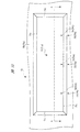
次に、図1に示すベースパッケージ6の構造について説明する。図2は図1に示すベースパッケージの上面側の内部構造を示す透視平面図である。なお、図2では、主面側の各部材の配置を示すため、図1に示す封止樹脂16を取り除いた状態で示している。
次に、図1に示すサブパッケージ7の構造について説明する。図3は図1に示すサブパッケージの上面側を示す平面図である。
次に本実施の形態の半導体装置の製造方法について説明する。本実施の形態の半導体装置の製造方法は、ベースパッケージ6(封止樹脂16を除く)、およびサブ基板5に相当する基材をそれぞれ準備する基材準備工程を有している。また、ベースパッケージ6およびサブ基板5を離間した状態で配置して、ベース基板3の主面3aとサブ基板5の裏面5bの間に樹脂を供給して封止樹脂16を形成する封止工程を有している。また、封止樹脂16を形成した後、サブ基板5の主面5a側からベース基板3の上面側に向かって貫通孔を形成し、貫通孔内に導電性部材を形成してサブ基板5とベース基板3を電気的に接続する電気的接続工程を含んでいる。
ピン54、55は、封止工程において図4〜図8のいずれかに示すベース基板30とサブ基板40の位置合わせを行うために用いる突起であり、キャビティ51の底面51a、あるいは上面52から、上型50bの下面53に向かって突出するように形成されている。
前記実施の形態1では、2枚の配線基板(基材)を積層した半導体装置の実施態様について説明したが、積層する配線基板の数は2枚に限定されない。本実施の形態2では、3枚以上の配線基板(基材)を積層する実施態様について説明する。なお、本実施の形態では、前記実施の形態1との相違点を中心に説明し、前記実施の形態1と重複する説明は原則として省略する。
次に、ベース基板上に複数枚の配線基板を積層する第1の変形例について説明する。図33は第1の変形例である半導体装置の全体構造を示す断面図である。図33に示すPOP70と図29に示すPOP60の相違点は、基板間接続用のランド(端子)の配置である。
次に、ベース基板上に複数枚の配線基板を積層する第2の変形例について説明する。図34は第2の変形例である半導体装置の全体構造を示す断面図である。図34に示すPOP71と図29に示すPOP60の相違点は、中段に配置されるサブ基板72の主面5a上にチップ部品4が搭載されていない点である。また、サブ基板72の主面5aには、上段に配置されるサブ基板5と電気的に接続される配線73が形成されている。
次に、複数枚の配線基板を積層する第3の変形例について説明する。図35は第3の変形例である半導体装置の全体構造を示す断面図である。図35に示すPOP74と図34に示すPOP71との相違点は、基板間の接続構造である。POP74の最上段に搭載されるサブパッケージ75が有するサブ基板76は主面5aに中段に配置されるサブ基板72と電気的に接続される複数のランド22に加え、ベース基板3と電気的に接続される複数のランド77を有している。詳しくは、ランド22は半田材8を介してサブ基板72の主面5aに形成されたランド64と電気的に接続されている。また、ランド77は、複数のサブ基板5および複数の封止樹脂16、61を貫通して形成される半田材8を介してベース基板30のランド12と電気的に接続されている。また、ランド22およびランド77は、それぞれ図示しない配線を介してサブ基板76に搭載されたチップ部品4と電気的に接続されている。前記した第2の変形例と同様に、図35に示す第3の変形例の場合にも、主面5a側に電子部品が搭載されていないサブ基板72を中段に配置し、これをサブ基板5と電気的に接続することにより、配線引き回しのスペースを拡大することができる。
図35に示すPOP74は、前記実施の形態1で説明した製造方法を応用し、前記第3の変形例とは別の製造方法によっても製造することができる。以下別の製造方法について、第4の変形例として説明する。図36は本変形例の第1の基材配置工程において、成型金型のキャビティ内に複数枚の配線基板を配置した状態を示す要部拡大断面図、図37は図36に示す下型の上面を示す要部拡大平面図、図38は図36に示す位置決めピン周辺を拡大して示す要部拡大断面図、図39は図36に示す支持台周辺を示す要部拡大断面図である。
2 半導体チップ
2a 主面
2b 裏面
2c 側面
2d パッド
3 ベース基板
3a 主面
3b 裏面
3c チップ搭載領域
4、4A、4B チップ部品
4a 上面
4b 下面
4c 側面
4d 端子
5 サブ基板
5a 主面
5b 裏面
5c チップ部品搭載領域
6 ベースパッケージ
7 サブパッケージ
8 半田材
11 端子
12 ランド
13 ランド
14 配線
15 ワイヤ
16 封止樹脂
17 半田ボール
21 端子
22 ランド
23 半田材
24 配線
30 ベース基板
30a 製品形成領域
30b 枠部
30c 長辺
30d 短辺
31、31a、31b 孔部
40 サブ基板
40a 製品形成領域
40b 枠部
40c 長辺
40d 短辺
41、41a、41b 孔部
42 矢印
43 矢印
45 一括封止構造体
46 貫通孔
47 積層配線基板
50 成型金型
50a 下型
50b 上型
51 キャビティ
51a 底面
51c 長辺
51d 短辺
52 上面
53 下面
54、54a、54b、55、55a、55b ピン
61 封止樹脂
62、65、75 サブパッケージ
63、68、72、76、78、79 サブ基板
64、77 ランド
66、80 成型金型
66a、80a 下型
67、81 キャビティ
69 一括封止構造体
73 配線
78a 孔部
78b 孔部
79a 孔部
79b 孔部
82 ピン
82a 受け面
82b 受け部
82c 突出部
83 支持台
83a 受け面
Wa、Wb 開口幅
Wc 開口径
Wd、We 幅
Claims (5)
- 以下の工程を含むことを特徴とする半導体装置の製造方法:
(a)第1面を有する第1金型、および凹部が形成され、前記第1面と対向する第2面を有する第2金型を備えた成型金型を準備する工程;
(b)第1主面、前記第1主面に形成された複数の第1電極パッド、前記複数の第1電極パッドとそれぞれ接続された複数の第1配線、前記複数の第1配線とそれぞれ接続された複数の第1ランド、および前記第1主面とは反対側の第1裏面を有する第1基材を、前記第1主面が前記第2金型の前記凹部と対向するように、前記第2金型の前記凹部内に配置する工程;
(c)前記(b)工程の後、第2主面、前記第2主面に形成された複数の第2電極パッド、前記複数の第2電極パッドとそれぞれ接続された複数の第2配線、前記複数の第2配線とそれぞれ接続された複数の第2ランド、および前記第2主面とは反対側の第2裏面を有し、前記第2主面に半導体チップが搭載された第2基材を、前記第2主面が前記第1基材の前記第1裏面と対向するように、前記第1金型と前記第2金型との間に配置する工程;
(d)前記(c)工程の後、前記第2基材を前記第1金型と前記第2金型でクランプする工程;
(e)前記(d)工程の後、前記第1基材と前記第2基材との間に樹脂を供給し、前記第1基材と前記第2基材との間に封止体を形成する工程;
(f)前記(e)工程の後、前記第1金型と前記第2金型との間から、前記封止体が形成された前記第1基材および前記第2基材を取り出す工程;
(g)前記(f)工程の後、前記第1基材の前記第1ランドから前記第2基材の前記第2ランドに向かって貫通孔を形成し、前記第2ランドを露出させる工程;
(h)前記(g)工程の後、前記貫通孔の内部に導電性部材を形成する工程。 - 請求項1において、
前記第1基材は、前記第1主面から前記第1裏面に向かって形成された第1孔部を有し、
前記(b)工程では、前記第2金型の前記凹部に形成された第1ピンが前記第1基材の前記第1孔部内に位置するように、前記第1基材を前記第2金型の前記凹部内に配置し、
前記第2基材は、前記第2主面から前記第2裏面に向かって形成された第2孔部を有し、
前記(c)工程では、前記第2金型の前記第2面に形成された第2ピンが前記第2基材の前記第2孔部内に位置するように、前記第2基材を前記第1金型と第2金型との間に配置することを特徴とする半導体装置の製造方法。 - 請求項2において、
前記第1基材の前記第1主面、および前記第2基材の前記第2主面は、それぞれ四角形の平面形状を成し、
前記第1孔部は、前記第1主面の4辺のうち、第1の辺に近づけて配置され、
前記第2孔部は、前記第2主面の4辺のうち、前記第1の辺に沿って配置される第2の辺に近づけて配置されていることを特徴とする半導体装置の製造方法。 - 請求項3において、
前記第1孔部は、前記第1の辺に沿って複数形成され、前記第2孔部は前記第2の辺に沿って複数形成されていることを特徴とする半導体装置の製造方法。 - 請求項4において、
前記第1孔部は、前記第1の辺の中央に配置される第1中央孔部と、前記第1の辺に沿って前記第1中央孔部の両サイドに配置される第1サイド孔部を有し、
前記第2孔部は、前記第2の辺の中央に配置される第2中央孔部と、前記第2の辺に沿って前記第2中央孔部の両サイドに配置される第2サイド孔部を有し、
前記第1サイド孔部の開口面積は、前記第1中央孔部の開口面積よりも広く、
前記第2サイド孔部の開口面積は、前記第2中央孔部の開口面積よりも広いことを特徴とする半導体装置の製造方法。
Priority Applications (2)
| Application Number | Priority Date | Filing Date | Title |
|---|---|---|---|
| JP2009226679A JP5149881B2 (ja) | 2009-09-30 | 2009-09-30 | 半導体装置の製造方法 |
| US12/834,937 US8293575B2 (en) | 2009-09-30 | 2010-07-13 | Manufacturing method of semiconductor device |
Applications Claiming Priority (1)
| Application Number | Priority Date | Filing Date | Title |
|---|---|---|---|
| JP2009226679A JP5149881B2 (ja) | 2009-09-30 | 2009-09-30 | 半導体装置の製造方法 |
Publications (3)
| Publication Number | Publication Date |
|---|---|
| JP2011077267A JP2011077267A (ja) | 2011-04-14 |
| JP2011077267A5 JP2011077267A5 (ja) | 2012-06-14 |
| JP5149881B2 true JP5149881B2 (ja) | 2013-02-20 |
Family
ID=43780836
Family Applications (1)
| Application Number | Title | Priority Date | Filing Date |
|---|---|---|---|
| JP2009226679A Expired - Fee Related JP5149881B2 (ja) | 2009-09-30 | 2009-09-30 | 半導体装置の製造方法 |
Country Status (2)
| Country | Link |
|---|---|
| US (1) | US8293575B2 (ja) |
| JP (1) | JP5149881B2 (ja) |
Families Citing this family (11)
| Publication number | Priority date | Publication date | Assignee | Title |
|---|---|---|---|---|
| JP5241909B2 (ja) | 2011-12-22 | 2013-07-17 | 太陽誘電株式会社 | 回路基板 |
| JP5241910B2 (ja) * | 2011-12-22 | 2013-07-17 | 太陽誘電株式会社 | 回路基板 |
| JP6021386B2 (ja) * | 2012-03-30 | 2016-11-09 | オリンパス株式会社 | 配線基板の製造方法、並びに半導体装置の製造方法 |
| ITTO20120374A1 (it) * | 2012-04-27 | 2013-10-28 | St Microelectronics Srl | Struttura a semiconduttore con regioni conduttive a bassa temperatura di fusione e metodo per riparare una struttura a semiconduttore |
| KR20140055728A (ko) * | 2012-11-01 | 2014-05-09 | 엘지전자 주식회사 | 백라이트 유닛 및 디스플레이 장치 |
| CN103199713A (zh) * | 2013-04-09 | 2013-07-10 | 黄山市祁门新飞电子科技发展有限公司 | 环保型桥式整流器 |
| JP2015015442A (ja) | 2013-07-08 | 2015-01-22 | 三菱電機株式会社 | 半導体装置 |
| US9673173B1 (en) * | 2015-07-24 | 2017-06-06 | Altera Corporation | Integrated circuit package with embedded passive structures |
| JP7604815B2 (ja) | 2020-09-10 | 2024-12-24 | 富士電機株式会社 | 半導体装置および半導体装置の製造方法 |
| US11729915B1 (en) | 2022-03-22 | 2023-08-15 | Tactotek Oy | Method for manufacturing a number of electrical nodes, electrical node module, electrical node, and multilayer structure |
| JP2024179920A (ja) * | 2023-06-16 | 2024-12-26 | Towa株式会社 | 樹脂成形システム及び樹脂成形品の製造方法 |
Family Cites Families (8)
| Publication number | Priority date | Publication date | Assignee | Title |
|---|---|---|---|---|
| JP2514818B2 (ja) * | 1987-06-18 | 1996-07-10 | ナイルス部品株式会社 | 集積回路基板の樹脂封止方法 |
| US5910255A (en) * | 1996-11-08 | 1999-06-08 | W. L. Gore & Associates, Inc. | Method of sequential laser processing to efficiently manufacture modules requiring large volumetric density material removal for micro-via formation |
| JP2001007130A (ja) * | 1999-06-21 | 2001-01-12 | Mitsubishi Electric Corp | 半導体装置の製造装置および製造方法 |
| JP3660861B2 (ja) * | 2000-08-18 | 2005-06-15 | 株式会社ルネサステクノロジ | 半導体装置の製造方法 |
| US6840751B2 (en) * | 2002-08-22 | 2005-01-11 | Texas Instruments Incorporated | Vertical mold die press machine |
| US7189601B2 (en) * | 2004-03-02 | 2007-03-13 | Texas Instruments Incorporated | System and method for forming mold caps over integrated circuit devices |
| JP4553765B2 (ja) * | 2005-03-25 | 2010-09-29 | Okiセミコンダクタ株式会社 | 半導体装置の製造方法 |
| JP5036397B2 (ja) | 2007-05-21 | 2012-09-26 | 新光電気工業株式会社 | チップ内蔵基板の製造方法 |
-
2009
- 2009-09-30 JP JP2009226679A patent/JP5149881B2/ja not_active Expired - Fee Related
-
2010
- 2010-07-13 US US12/834,937 patent/US8293575B2/en not_active Expired - Fee Related
Also Published As
| Publication number | Publication date |
|---|---|
| US8293575B2 (en) | 2012-10-23 |
| JP2011077267A (ja) | 2011-04-14 |
| US20110076800A1 (en) | 2011-03-31 |
Similar Documents
| Publication | Publication Date | Title |
|---|---|---|
| JP5149881B2 (ja) | 半導体装置の製造方法 | |
| JP5425584B2 (ja) | 半導体装置の製造方法 | |
| TWI645465B (zh) | 半導體裝置及其製造方法 | |
| JP5271886B2 (ja) | 半導体装置およびその製造方法 | |
| US8389339B2 (en) | Method of manufacturing semiconductor device | |
| US8575763B2 (en) | Semiconductor device and method of manufacturing the same | |
| US8076787B2 (en) | Semiconductor device, manufacturing method thereof, and manufacturing method of semiconductor module | |
| JP2011040602A (ja) | 電子装置およびその製造方法 | |
| CN109037184B (zh) | 半导体器件 | |
| US9640414B2 (en) | Method of manufacturing semiconductor device | |
| JP2010287710A (ja) | 半導体装置およびその製造方法 | |
| US10304767B2 (en) | Semiconductor device | |
| JP2012028513A (ja) | 半導体装置及びその製造方法 | |
| KR101474189B1 (ko) | 집적회로 패키지 | |
| TW202226464A (zh) | 具有堆疊被動組件的多層半導體封裝 | |
| JP2011211159A (ja) | 半導体装置の製造方法 | |
| JP2010010269A (ja) | 半導体装置、半導体装置製造用中間体およびそれらの製造方法 | |
| JP5286303B2 (ja) | 半導体装置の製造方法 | |
| JP2011165793A (ja) | 半導体装置及びその製造方法、並びに電子装置 | |
| JP2007294560A (ja) | 半導体装置およびその製造方法 | |
| KR101432486B1 (ko) | 집적회로 패키지 제조방법 | |
| JP2006294832A (ja) | 半導体装置の製造方法 | |
| JP2015015362A (ja) | 半導体装置の製造方法 | |
| US20070273010A1 (en) | Design and Method for Attaching a Die to a Leadframe in a Semiconductor Device | |
| JP2005057099A (ja) | 半導体装置およびその製造方法 |
Legal Events
| Date | Code | Title | Description |
|---|---|---|---|
| A521 | Request for written amendment filed |
Free format text: JAPANESE INTERMEDIATE CODE: A523 Effective date: 20120425 |
|
| A621 | Written request for application examination |
Free format text: JAPANESE INTERMEDIATE CODE: A621 Effective date: 20120425 |
|
| A977 | Report on retrieval |
Free format text: JAPANESE INTERMEDIATE CODE: A971007 Effective date: 20121022 |
|
| TRDD | Decision of grant or rejection written | ||
| A01 | Written decision to grant a patent or to grant a registration (utility model) |
Free format text: JAPANESE INTERMEDIATE CODE: A01 Effective date: 20121106 |
|
| A61 | First payment of annual fees (during grant procedure) |
Free format text: JAPANESE INTERMEDIATE CODE: A61 Effective date: 20121130 |
|
| R150 | Certificate of patent or registration of utility model |
Ref document number: 5149881 Country of ref document: JP Free format text: JAPANESE INTERMEDIATE CODE: R150 Free format text: JAPANESE INTERMEDIATE CODE: R150 |
|
| FPAY | Renewal fee payment (event date is renewal date of database) |
Free format text: PAYMENT UNTIL: 20151207 Year of fee payment: 3 |
|
| S531 | Written request for registration of change of domicile |
Free format text: JAPANESE INTERMEDIATE CODE: R313531 |
|
| R350 | Written notification of registration of transfer |
Free format text: JAPANESE INTERMEDIATE CODE: R350 |
|
| LAPS | Cancellation because of no payment of annual fees |