JP5014139B2 - 表示装置およびカラーフィルタ基板 - Google Patents
表示装置およびカラーフィルタ基板 Download PDFInfo
- Publication number
- JP5014139B2 JP5014139B2 JP2007536483A JP2007536483A JP5014139B2 JP 5014139 B2 JP5014139 B2 JP 5014139B2 JP 2007536483 A JP2007536483 A JP 2007536483A JP 2007536483 A JP2007536483 A JP 2007536483A JP 5014139 B2 JP5014139 B2 JP 5014139B2
- Authority
- JP
- Japan
- Prior art keywords
- pixel
- sub
- red
- display device
- green
- Prior art date
- Legal status (The legal status is an assumption and is not a legal conclusion. Google has not performed a legal analysis and makes no representation as to the accuracy of the status listed.)
- Expired - Fee Related
Links
- 239000000758 substrate Substances 0.000 title claims description 26
- 239000004973 liquid crystal related substance Substances 0.000 claims description 71
- 239000003086 colorant Substances 0.000 description 43
- 230000003595 spectral effect Effects 0.000 description 20
- 238000001228 spectrum Methods 0.000 description 20
- 238000002834 transmittance Methods 0.000 description 20
- 239000011159 matrix material Substances 0.000 description 10
- 238000000034 method Methods 0.000 description 9
- 238000004040 coloring Methods 0.000 description 7
- 238000010586 diagram Methods 0.000 description 7
- 239000000654 additive Substances 0.000 description 5
- 230000000996 additive effect Effects 0.000 description 5
- 230000000295 complement effect Effects 0.000 description 5
- 230000000694 effects Effects 0.000 description 5
- 238000006243 chemical reaction Methods 0.000 description 3
- 230000007423 decrease Effects 0.000 description 3
- 238000004519 manufacturing process Methods 0.000 description 3
- 238000013507 mapping Methods 0.000 description 3
- 239000000203 mixture Substances 0.000 description 2
- 229920006395 saturated elastomer Polymers 0.000 description 2
- LEYJJTBJCFGAQN-UHFFFAOYSA-N chembl1985378 Chemical compound OC1=CC=C2C=CC=CC2=C1N=NC(C=C1)=CC=C1N=NC1=CC=C(S(O)(=O)=O)C=C1 LEYJJTBJCFGAQN-UHFFFAOYSA-N 0.000 description 1
- 230000003247 decreasing effect Effects 0.000 description 1
- 238000013461 design Methods 0.000 description 1
- 239000011521 glass Substances 0.000 description 1
- 238000011160 research Methods 0.000 description 1
- 238000012795 verification Methods 0.000 description 1
Images


Classifications
-
- G—PHYSICS
- G09—EDUCATION; CRYPTOGRAPHY; DISPLAY; ADVERTISING; SEALS
- G09G—ARRANGEMENTS OR CIRCUITS FOR CONTROL OF INDICATING DEVICES USING STATIC MEANS TO PRESENT VARIABLE INFORMATION
- G09G3/00—Control arrangements or circuits, of interest only in connection with visual indicators other than cathode-ray tubes
- G09G3/20—Control arrangements or circuits, of interest only in connection with visual indicators other than cathode-ray tubes for presentation of an assembly of a number of characters, e.g. a page, by composing the assembly by combination of individual elements arranged in a matrix no fixed position being assigned to or needed to be assigned to the individual characters or partial characters
- G09G3/2003—Display of colours
-
- G—PHYSICS
- G02—OPTICS
- G02F—OPTICAL DEVICES OR ARRANGEMENTS FOR THE CONTROL OF LIGHT BY MODIFICATION OF THE OPTICAL PROPERTIES OF THE MEDIA OF THE ELEMENTS INVOLVED THEREIN; NON-LINEAR OPTICS; FREQUENCY-CHANGING OF LIGHT; OPTICAL LOGIC ELEMENTS; OPTICAL ANALOGUE/DIGITAL CONVERTERS
- G02F1/00—Devices or arrangements for the control of the intensity, colour, phase, polarisation or direction of light arriving from an independent light source, e.g. switching, gating or modulating; Non-linear optics
- G02F1/01—Devices or arrangements for the control of the intensity, colour, phase, polarisation or direction of light arriving from an independent light source, e.g. switching, gating or modulating; Non-linear optics for the control of the intensity, phase, polarisation or colour
- G02F1/13—Devices or arrangements for the control of the intensity, colour, phase, polarisation or direction of light arriving from an independent light source, e.g. switching, gating or modulating; Non-linear optics for the control of the intensity, phase, polarisation or colour based on liquid crystals, e.g. single liquid crystal display cells
- G02F1/133—Constructional arrangements; Operation of liquid crystal cells; Circuit arrangements
- G02F1/1333—Constructional arrangements; Manufacturing methods
- G02F1/1335—Structural association of cells with optical devices, e.g. polarisers or reflectors
- G02F1/133509—Filters, e.g. light shielding masks
- G02F1/133514—Colour filters
-
- G—PHYSICS
- G02—OPTICS
- G02F—OPTICAL DEVICES OR ARRANGEMENTS FOR THE CONTROL OF LIGHT BY MODIFICATION OF THE OPTICAL PROPERTIES OF THE MEDIA OF THE ELEMENTS INVOLVED THEREIN; NON-LINEAR OPTICS; FREQUENCY-CHANGING OF LIGHT; OPTICAL LOGIC ELEMENTS; OPTICAL ANALOGUE/DIGITAL CONVERTERS
- G02F2201/00—Constructional arrangements not provided for in groups G02F1/00 - G02F7/00
- G02F2201/52—RGB geometrical arrangements
-
- G—PHYSICS
- G09—EDUCATION; CRYPTOGRAPHY; DISPLAY; ADVERTISING; SEALS
- G09G—ARRANGEMENTS OR CIRCUITS FOR CONTROL OF INDICATING DEVICES USING STATIC MEANS TO PRESENT VARIABLE INFORMATION
- G09G2300/00—Aspects of the constitution of display devices
- G09G2300/04—Structural and physical details of display devices
- G09G2300/0439—Pixel structures
- G09G2300/0452—Details of colour pixel setup, e.g. pixel composed of a red, a blue and two green components
-
- G—PHYSICS
- G09—EDUCATION; CRYPTOGRAPHY; DISPLAY; ADVERTISING; SEALS
- G09G—ARRANGEMENTS OR CIRCUITS FOR CONTROL OF INDICATING DEVICES USING STATIC MEANS TO PRESENT VARIABLE INFORMATION
- G09G2340/00—Aspects of display data processing
- G09G2340/06—Colour space transformation
-
- G—PHYSICS
- G09—EDUCATION; CRYPTOGRAPHY; DISPLAY; ADVERTISING; SEALS
- G09G—ARRANGEMENTS OR CIRCUITS FOR CONTROL OF INDICATING DEVICES USING STATIC MEANS TO PRESENT VARIABLE INFORMATION
- G09G3/00—Control arrangements or circuits, of interest only in connection with visual indicators other than cathode-ray tubes
- G09G3/20—Control arrangements or circuits, of interest only in connection with visual indicators other than cathode-ray tubes for presentation of an assembly of a number of characters, e.g. a page, by composing the assembly by combination of individual elements arranged in a matrix no fixed position being assigned to or needed to be assigned to the individual characters or partial characters
- G09G3/34—Control arrangements or circuits, of interest only in connection with visual indicators other than cathode-ray tubes for presentation of an assembly of a number of characters, e.g. a page, by composing the assembly by combination of individual elements arranged in a matrix no fixed position being assigned to or needed to be assigned to the individual characters or partial characters by control of light from an independent source
- G09G3/36—Control arrangements or circuits, of interest only in connection with visual indicators other than cathode-ray tubes for presentation of an assembly of a number of characters, e.g. a page, by composing the assembly by combination of individual elements arranged in a matrix no fixed position being assigned to or needed to be assigned to the individual characters or partial characters by control of light from an independent source using liquid crystals
- G09G3/3607—Control arrangements or circuits, of interest only in connection with visual indicators other than cathode-ray tubes for presentation of an assembly of a number of characters, e.g. a page, by composing the assembly by combination of individual elements arranged in a matrix no fixed position being assigned to or needed to be assigned to the individual characters or partial characters by control of light from an independent source using liquid crystals for displaying colours or for displaying grey scales with a specific pixel layout, e.g. using sub-pixels
Landscapes
- Physics & Mathematics (AREA)
- Engineering & Computer Science (AREA)
- Nonlinear Science (AREA)
- General Physics & Mathematics (AREA)
- Chemical & Material Sciences (AREA)
- Mathematical Physics (AREA)
- Theoretical Computer Science (AREA)
- Crystallography & Structural Chemistry (AREA)
- Computer Hardware Design (AREA)
- Optics & Photonics (AREA)
- Liquid Crystal (AREA)
- Optical Filters (AREA)
- Devices For Indicating Variable Information By Combining Individual Elements (AREA)
Description
R2 第2の赤サブ画素
G 緑サブ画素
B 青サブ画素
Ye 黄サブ画素
C シアンサブ画素
10 アクティブマトリクス基板
11 スイッチング素子
20 カラーフィルタ基板
21 透明基板
22R1 第1の赤カラーフィルタ
22R2 第2の赤カラーフィルタ
22G 緑カラーフィルタ
22B 青カラーフィルタ
22Ye 黄カラーフィルタ
22C シアンカラーフィルタ
23 ブラックマトリクス
24 対向電極
30 液晶層
40 多原色コントローラ
41 変換マトリクス
42 マッピングユニット
43 2次元ルックアップテーブル
44 乗算器
100、200 液晶表示装置

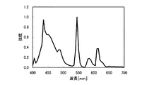
表7に、本実施例における各サブ画素のY値、xy色度、主波長、色純度および表示品位を示し、表8に、本実施例における各原色のY値、xy色度、主波長(マゼンタについては補色主波長)、色純度および表示品位を示す。また、本実施例におけるカラーフィルタの分光透過率特性およびバックライトのスペクトルを、図11および図12に示す。
表9に、本実施例における各サブ画素のY値等を示し、表10に、本実施例における各原色のY値等を示す。また、本実施例におけるカラーフィルタの分光透過率特性およびバックライトのスペクトルを、図13および図14に示す。
表11に、本実施例における各サブ画素のY値等を示し、表12に、本実施例における各原色のY値等を示す。また、本実施例におけるカラーフィルタの分光透過率特性およびバックライトのスペクトルを、図15および図16に示す。
表13に、本実施例における各サブ画素のY値等を示し、表14に、本実施例における各原色のY値等を示す。また、本実施例におけるカラーフィルタの分光透過率特性およびバックライトのスペクトルを、図17および図18に示す。
表15に、本実施例における各サブ画素のY値等を示し、表16に、本実施例における各原色のY値等を示す。また、本実施例におけるカラーフィルタの分光透過率特性およびバックライトのスペクトルを、図19および図20に示す。
表17に、本実施例における各サブ画素のY値等を示し、表18に、本実施例における各原色のY値等を示す。また、本実施例におけるカラーフィルタの分光透過率特性およびバックライトのスペクトルを、図21および図22に示す。
表19に、本実施例における各サブ画素のY値等を示し、表20に、本実施例における各原色のY値等を示す。また、本実施例におけるカラーフィルタの分光透過率特性およびバックライトのスペクトルを、図23および図24に示す。
表21に、本実施例における各サブ画素のY値等を示し、表22に、本実施例における各原色のY値等を示す。また、本実施例におけるカラーフィルタの分光透過率特性およびバックライトのスペクトルを、図25および図26に示す。
Electron-emitter Display)に好適に用いられる。
Claims (26)
- 複数のサブ画素によって規定される画素を有する表示装置であって、
前記複数のサブ画素は、赤を表示する第1および第2の赤サブ画素、緑を表示する緑サブ画素、青を表示する青サブ画素および黄を表示する黄サブ画素を含み、
前記画素が白を表示したときのXYZ表色系におけるY値を100%としたとき、前記第1および第2の赤サブ画素によって表示される赤のY値は10%以上22%以下である表示装置。 - 前記緑サブ画素によって表示される緑のY値は20%以上35%以下、前記青サブ画素によって表示される青のY値は5%以上10%以下、前記第1の赤サブ画素、前記第2の赤サブ画素、前記緑サブ画素および前記黄サブ画素によって表示される黄のY値は60%以上85%以下である請求項1に記載の表示装置。
- 前記第1の赤サブ画素、前記第2の赤サブ画素および前記青サブ画素によって表示されるマゼンタのY値は15%以上30%以下である請求項2に記載の表示装置。
- 前記第1および第2の赤サブ画素によって表示される赤の主波長は605nm以上635nm以下、前記緑サブ画素によって表示される緑の主波長は520nm以上550nm以下、前記青サブ画素によって表示される青の主波長は470nm以下、前記第1の赤サブ画素、前記第2の赤サブ画素、前記緑サブ画素および前記黄サブ画素によって表示される黄の主波長は565nm以上580nm以下である、請求項1から3のいずれかに記載の表示装置。
- 前記第1および第2の赤サブ画素によって表示される赤の色純度は90%以上、前記緑サブ画素によって表示される緑の色純度は65%以上80%以下、前記青サブ画素によって表示される青の色純度は90%以上95%以下、前記第1の赤サブ画素、前記第2の赤サブ画素、前記緑サブ画素および前記黄サブ画素によって表示される黄の色純度は85%以上95%以下である請求項1から4のいずれかに記載の表示装置。
- 前記第1の赤サブ画素、前記第2の赤サブ画素および前記青サブ画素によって表示されるマゼンタの色純度は60%以上80%以下である請求項5に記載の表示装置。
- 前記第1および第2の赤サブ画素の主波長はそれぞれ605nm以上635nm以下、前記緑サブ画素の主波長は520nm以上550nm以下、前記青サブ画素の主波長は470nm以下、前記黄サブ画素の主波長は565nm以上580nm以下である請求項1から6のいずれかに記載の表示装置。
- 前記第1および第2の赤サブ画素のそれぞれの色純度は90%以上、前記緑サブ画素の色純度は65%以上80%以下、前記青サブ画素の色純度は90%以上95%以下、前記黄サブ画素の色純度は85%以上95%以下である請求項1から7のいずれかに記載の表示装置。
- 前記複数のサブ画素は、実質的に同じ大きさを有する請求項1から8のいずれかに記載の表示装置。
- 前記第1および第2の赤サブ画素は互いに独立に駆動される請求項1から9のいずれかに記載の表示装置。
- 前記第1および第2の赤サブ画素は同一のスイッチング素子によって駆動される請求項1から9のいずれかに記載の表示装置。
- 前記画素内において、前記第1の赤サブ画素と前記第2の赤サブ画素とが連続するように配置されている請求項1から11のいずれかに記載の表示装置。
- 前記画素内において、前記緑サブ画素と前記黄サブ画素とが連続し、且つ、他のサブ画素によって挟まれるように配置されている請求項1から12のいずれかに記載の表示装置。
- 前記画素内において、前記第1の赤サブ画素、前記第2の赤サブ画素、前記緑サブ画素および前記黄サブ画素が連続するように配置されている請求項1から13のいずれかに記載の表示装置。
- 前記複数のサブ画素は、シアンを表示するシアンサブ画素をさらに含む請求項1から14のいずれかに記載の表示装置。
- 前記画素が白を表示したときのXYZ表色系におけるY値を100%としたとき、前記緑サブ画素、前記青サブ画素および前記シアンサブ画素によって表示されるシアンのY値は10%以上55%以下である請求項15に記載の表示装置。
- 前記緑サブ画素、前記青サブ画素および前記シアンサブ画素によって表示されるシアンの主波長は475nm以上500nm以下である請求項15または16に記載の表示装置。
- 前記緑サブ画素、前記青サブ画素および前記シアンサブ画素によって表示されるシアンの色純度は65%以上80%以下である請求項15から17のいずれかに記載の表示装置。
- 前記画素は、前記第1および第2の赤サブ画素、前記緑サブ画素、前記青サブ画素、前記黄サブ画素および前記シアンサブ画素によって規定され、
前記画素が白を表示したときのXYZ表色系におけるY値を100%としたとき、前記シアンサブ画素のY値は10%以上30%以下である請求項15から18のいずれかに記載の表示装置。 - 前記第1および第2の赤サブ画素のY値はそれぞれ5%以上11%以下、前記緑サブ画素のY値は20%以上35%以下、前記青サブ画素のY値は5%以上10%以下、前記黄サブ画素のY値は30%以上50%以下である請求項19に記載の表示装置。
- 前記シアンサブ画素の主波長は475nm以上500nm以下である請求項15から20のいずれかに記載の表示装置。
- 前記シアンサブ画素の色純度は65%以上80%以下である請求項15から21のいずれかに記載の表示装置。
- 前記画素内において、前記シアンサブ画素、前記緑サブ画素および前記青サブ画素が連続するように配置されている請求項15から22のいずれかに記載の表示装置。
- 液晶層を備えた液晶表示装置である請求項1から23のいずれかに記載の表示装置。
- 複数のサブ画素によって規定される画素を有する表示装置用のカラーフィルタ基板であって、
基板と、
前記基板上の前記画素に対応する領域内に設けられた複数のカラーフィルタとを備え、
前記複数のカラーフィルタは、赤色の光を透過する第1および第2の赤カラーフィルタ、緑色の光を透過する緑カラーフィルタ、青色の光を透過する青カラーフィルタおよび黄色の光を透過する黄カラーフィルタを含み、
前記第1および第2の赤カラーフィルタは、同一画素に対応する領域内に設けられており、
前記第1および第2の赤カラーフィルタのY値の合計は、10%以上22%以下であるカラーフィルタ基板。 - 前記複数のカラーフィルタは、シアン色の光を透過するシアンカラーフィルタをさらに含む請求項25に記載のカラーフィルタ基板。
Priority Applications (1)
| Application Number | Priority Date | Filing Date | Title |
|---|---|---|---|
| JP2007536483A JP5014139B2 (ja) | 2005-09-21 | 2006-09-19 | 表示装置およびカラーフィルタ基板 |
Applications Claiming Priority (4)
| Application Number | Priority Date | Filing Date | Title |
|---|---|---|---|
| JP2005274510 | 2005-09-21 | ||
| JP2005274510 | 2005-09-21 | ||
| JP2007536483A JP5014139B2 (ja) | 2005-09-21 | 2006-09-19 | 表示装置およびカラーフィルタ基板 |
| PCT/JP2006/318486 WO2007034770A1 (ja) | 2005-09-21 | 2006-09-19 | 表示装置およびカラーフィルタ基板 |
Publications (2)
| Publication Number | Publication Date |
|---|---|
| JPWO2007034770A1 JPWO2007034770A1 (ja) | 2009-03-26 |
| JP5014139B2 true JP5014139B2 (ja) | 2012-08-29 |
Family
ID=37883554
Family Applications (1)
| Application Number | Title | Priority Date | Filing Date |
|---|---|---|---|
| JP2007536483A Expired - Fee Related JP5014139B2 (ja) | 2005-09-21 | 2006-09-19 | 表示装置およびカラーフィルタ基板 |
Country Status (6)
| Country | Link |
|---|---|
| US (2) | US7760177B2 (ja) |
| EP (1) | EP1927969B1 (ja) |
| JP (1) | JP5014139B2 (ja) |
| CN (2) | CN102122460B (ja) |
| TW (1) | TWI356224B (ja) |
| WO (1) | WO2007034770A1 (ja) |
Cited By (1)
| Publication number | Priority date | Publication date | Assignee | Title |
|---|---|---|---|---|
| KR102567648B1 (ko) * | 2016-03-14 | 2023-08-17 | 삼성디스플레이 주식회사 | 액정 표시 장치 |
Families Citing this family (44)
| Publication number | Priority date | Publication date | Assignee | Title |
|---|---|---|---|---|
| JP4265546B2 (ja) * | 2005-01-31 | 2009-05-20 | ソニー株式会社 | 撮像装置、画像処理装置および画像処理方法 |
| JP4528859B2 (ja) * | 2006-06-19 | 2010-08-25 | シャープ株式会社 | 表示装置 |
| US9928786B2 (en) * | 2006-10-13 | 2018-03-27 | Sharp Kabushiki Kaisha | Display device and signal converting device |
| JP4913161B2 (ja) * | 2007-01-25 | 2012-04-11 | シャープ株式会社 | 多原色表示装置 |
| RU2442291C2 (ru) * | 2007-03-16 | 2012-02-10 | Шарп Кабусики Кайся | Устройство отображения |
| JP2008256819A (ja) * | 2007-04-03 | 2008-10-23 | Toppan Printing Co Ltd | 液晶表示装置用カラーフィルタ及び液晶表示装置 |
| KR100892225B1 (ko) * | 2007-04-16 | 2009-04-09 | 삼성전자주식회사 | 컬러 디스플레이 장치 |
| JP4967783B2 (ja) * | 2007-04-24 | 2012-07-04 | 凸版印刷株式会社 | 液晶表示装置 |
| JP5216256B2 (ja) * | 2007-06-28 | 2013-06-19 | 凸版印刷株式会社 | カラーフィルタおよび液晶表示装置 |
| US8654050B2 (en) * | 2007-09-13 | 2014-02-18 | Sharp Kabushiki Kaisha | Multiple-primary-color liquid crystal display device |
| JP5262335B2 (ja) * | 2008-06-17 | 2013-08-14 | 凸版印刷株式会社 | カラーフィルタ及び液晶表示装置 |
| WO2010013421A1 (ja) * | 2008-07-28 | 2010-02-04 | シャープ株式会社 | 多原色表示装置 |
| CN102227675B (zh) * | 2008-11-28 | 2014-05-28 | 夏普株式会社 | 多原色液晶显示装置和信号转换电路 |
| EP2485083A4 (en) | 2009-09-30 | 2013-08-14 | Sharp Kk | LIQUID CRYSTAL DISPLAY DEVICE |
| EP2495608A1 (en) * | 2009-10-29 | 2012-09-05 | Sharp Kabushiki Kaisha | Liquid crystal display device |
| WO2011093243A1 (ja) | 2010-01-29 | 2011-08-04 | シャープ株式会社 | 液晶表示装置 |
| JP5768424B2 (ja) * | 2011-03-22 | 2015-08-26 | ソニー株式会社 | 表示装置 |
| CN102749751B (zh) * | 2011-04-22 | 2015-09-16 | 群创光电股份有限公司 | 显示面板 |
| TWI484817B (zh) * | 2011-12-15 | 2015-05-11 | Au Optronics Corp | 顯示面板 |
| US8902265B2 (en) * | 2012-03-07 | 2014-12-02 | Eastman Kodak Company | Method for controlling display with alternating color pixels |
| US10229956B2 (en) | 2013-01-18 | 2019-03-12 | Universal Display Corporation | High resolution low power consumption OLED display with extended lifetime |
| US9590017B2 (en) | 2013-01-18 | 2017-03-07 | Universal Display Corporation | High resolution low power consumption OLED display with extended lifetime |
| US10580832B2 (en) | 2013-01-18 | 2020-03-03 | Universal Display Corporation | High resolution low power consumption OLED display with extended lifetime |
| US10243023B2 (en) | 2013-01-18 | 2019-03-26 | Universal Display Corporation | Top emission AMOLED displays using two emissive layers |
| US10304906B2 (en) | 2013-01-18 | 2019-05-28 | Universal Display Corporation | High resolution low power consumption OLED display with extended lifetime |
| TWI490614B (zh) | 2013-01-24 | 2015-07-01 | E Ink Holdings Inc | 電泳顯示裝置 |
| WO2014174895A1 (ja) * | 2013-04-26 | 2014-10-30 | シャープ株式会社 | 表示装置 |
| JP2015184623A (ja) * | 2014-03-26 | 2015-10-22 | ソニー株式会社 | 画像表示装置、カラーフィルタおよび画像信号処理装置 |
| US10700134B2 (en) * | 2014-05-27 | 2020-06-30 | Universal Display Corporation | Low power consumption OLED display |
| CN104460077B (zh) | 2014-12-31 | 2018-01-12 | 深圳市华星光电技术有限公司 | 像素单元结构及显示装置 |
| US9818804B2 (en) | 2015-09-18 | 2017-11-14 | Universal Display Corporation | Hybrid display |
| US10263050B2 (en) | 2015-09-18 | 2019-04-16 | Universal Display Corporation | Hybrid display |
| CN105869524A (zh) * | 2016-04-29 | 2016-08-17 | 中山市宏晟祥光电照明科技有限公司 | Led灯珠光效增强型显示屏模组 |
| CN106647061B (zh) * | 2017-01-23 | 2018-11-23 | 武汉华星光电技术有限公司 | 像素结构及液晶显示面板 |
| CN106918959A (zh) * | 2017-03-24 | 2017-07-04 | 京东方科技集团股份有限公司 | 像素结构、显示面板以及显示装置 |
| US10768469B2 (en) * | 2017-04-28 | 2020-09-08 | Japan Display Inc. | Active matrix display device |
| US20190064515A1 (en) * | 2017-08-30 | 2019-02-28 | Innolux Corporation | Display device and electronic apparatus using the same |
| CN113759589A (zh) * | 2017-08-30 | 2021-12-07 | 群创光电股份有限公司 | 显示装置 |
| CN108153055B (zh) * | 2018-01-08 | 2020-08-04 | 昆山龙腾光电股份有限公司 | 背光模组和液晶显示器 |
| CN108732812B (zh) * | 2018-05-28 | 2021-05-14 | 厦门天马微电子有限公司 | 显示面板和显示装置 |
| US10797112B2 (en) | 2018-07-25 | 2020-10-06 | Universal Display Corporation | Energy efficient OLED TV |
| WO2021070236A1 (ja) * | 2019-10-08 | 2021-04-15 | シャープ株式会社 | 発光デバイス |
| TWI800162B (zh) * | 2021-12-16 | 2023-04-21 | 元太科技工業股份有限公司 | 彩色顯示裝置及彩色濾光陣列基板 |
| KR20230103653A (ko) * | 2021-12-31 | 2023-07-07 | 엘지디스플레이 주식회사 | 유기 발광 표시 장치 |
Citations (11)
| Publication number | Priority date | Publication date | Assignee | Title |
|---|---|---|---|---|
| JPH09251160A (ja) * | 1996-03-15 | 1997-09-22 | Fuji Xerox Co Ltd | 反射型カラー表示装置 |
| JPH10123501A (ja) * | 1996-08-26 | 1998-05-15 | Canon Inc | 表示装置 |
| JP2001242451A (ja) * | 2000-03-01 | 2001-09-07 | Fujitsu Ltd | 反射型表示素子用の反射側基板及び反射型表示素子 |
| JP2003107437A (ja) * | 2001-07-26 | 2003-04-09 | Seiko Epson Corp | 液晶装置用基板、液晶装置、及び、電子機器 |
| JP2004078218A (ja) * | 2002-08-14 | 2004-03-11 | Samsung Electronics Co Ltd | 液晶表示装置 |
| JP2004529396A (ja) * | 2001-06-11 | 2004-09-24 | ゲノア・テクノロジーズ・リミテッド | カラーディスプレイ用の装置、システム、および方法 |
| WO2004107025A2 (en) * | 2003-05-27 | 2004-12-09 | Genoa Color Technologies Ltd. | Multi-primary display with spectrally adapted back-illumination |
| WO2005057532A2 (en) * | 2003-12-15 | 2005-06-23 | Genoa Color Technologies Ltd. | Multi-primary liquid crystal display |
| JP2005523465A (ja) * | 2002-04-11 | 2005-08-04 | ジェノア・カラー・テクノロジーズ・リミテッド | 属性を向上させるカラー表示装置および方法 |
| JP2006047975A (ja) * | 2004-04-26 | 2006-02-16 | Mitsubishi Chemicals Corp | カラーフィルター用青色組成物、カラーフィルター及びカラー画像表示装置 |
| JP2010277095A (ja) * | 2004-08-19 | 2010-12-09 | Sharp Corp | 多原色表示装置及び液晶表示装置 |
Family Cites Families (18)
| Publication number | Priority date | Publication date | Assignee | Title |
|---|---|---|---|---|
| GB8604402D0 (en) * | 1986-02-21 | 1986-03-26 | Gen Electric Co Plc | Liquid crystal displays |
| US4800375A (en) | 1986-10-24 | 1989-01-24 | Honeywell Inc. | Four color repetitive sequence matrix array for flat panel displays |
| JP2527477B2 (ja) * | 1988-06-14 | 1996-08-21 | シャープ株式会社 | 絵素表示装置 |
| US5642176A (en) * | 1994-11-28 | 1997-06-24 | Canon Kabushiki Kaisha | Color filter substrate and liquid crystal display device |
| US5899550A (en) * | 1996-08-26 | 1999-05-04 | Canon Kabushiki Kaisha | Display device having different arrangements of larger and smaller sub-color pixels |
| JP4034022B2 (ja) | 2000-01-25 | 2008-01-16 | シャープ株式会社 | 液晶表示装置 |
| JP2001306023A (ja) | 2000-04-18 | 2001-11-02 | Seiko Epson Corp | 画像表示装置 |
| JP3873827B2 (ja) * | 2001-07-26 | 2007-01-31 | セイコーエプソン株式会社 | 液晶装置及び電子機器 |
| US20040051724A1 (en) * | 2002-09-13 | 2004-03-18 | Elliott Candice Hellen Brown | Four color arrangements of emitters for subpixel rendering |
| JP2003284084A (ja) * | 2002-03-20 | 2003-10-03 | Sony Corp | 画像処理装置および方法、並びに画像処理装置の製造方法 |
| JP4342200B2 (ja) | 2002-06-06 | 2009-10-14 | シャープ株式会社 | 液晶表示装置 |
| JP4248306B2 (ja) | 2002-06-17 | 2009-04-02 | シャープ株式会社 | 液晶表示装置 |
| JP4366988B2 (ja) * | 2003-05-01 | 2009-11-18 | セイコーエプソン株式会社 | 有機el装置および電子機器 |
| KR100943273B1 (ko) * | 2003-05-07 | 2010-02-23 | 삼성전자주식회사 | 4-컬러 변환 방법 및 그 장치와 이를 이용한 유기전계발광표시장치 |
| US7495722B2 (en) * | 2003-12-15 | 2009-02-24 | Genoa Color Technologies Ltd. | Multi-color liquid crystal display |
| KR101072375B1 (ko) * | 2003-12-29 | 2011-10-11 | 엘지디스플레이 주식회사 | 화소별 개구율 자동제어가 가능한 액정표시장치 |
| US7515122B2 (en) * | 2004-06-02 | 2009-04-07 | Eastman Kodak Company | Color display device with enhanced pixel pattern |
| KR101122229B1 (ko) * | 2004-10-05 | 2012-03-19 | 삼성전자주식회사 | 4색 액정 표시 장치 |
-
2006
- 2006-09-19 CN CN201110008456.9A patent/CN102122460B/zh active Active
- 2006-09-19 JP JP2007536483A patent/JP5014139B2/ja not_active Expired - Fee Related
- 2006-09-19 WO PCT/JP2006/318486 patent/WO2007034770A1/ja active Application Filing
- 2006-09-19 CN CN200680034319XA patent/CN101268499B/zh not_active Expired - Fee Related
- 2006-09-19 EP EP06798097.9A patent/EP1927969B1/en not_active Not-in-force
- 2006-09-20 US US11/533,392 patent/US7760177B2/en not_active Expired - Fee Related
- 2006-09-21 TW TW095135009A patent/TWI356224B/zh not_active IP Right Cessation
-
2010
- 2010-06-03 US US12/792,909 patent/US20100238102A1/en not_active Abandoned
Patent Citations (11)
| Publication number | Priority date | Publication date | Assignee | Title |
|---|---|---|---|---|
| JPH09251160A (ja) * | 1996-03-15 | 1997-09-22 | Fuji Xerox Co Ltd | 反射型カラー表示装置 |
| JPH10123501A (ja) * | 1996-08-26 | 1998-05-15 | Canon Inc | 表示装置 |
| JP2001242451A (ja) * | 2000-03-01 | 2001-09-07 | Fujitsu Ltd | 反射型表示素子用の反射側基板及び反射型表示素子 |
| JP2004529396A (ja) * | 2001-06-11 | 2004-09-24 | ゲノア・テクノロジーズ・リミテッド | カラーディスプレイ用の装置、システム、および方法 |
| JP2003107437A (ja) * | 2001-07-26 | 2003-04-09 | Seiko Epson Corp | 液晶装置用基板、液晶装置、及び、電子機器 |
| JP2005523465A (ja) * | 2002-04-11 | 2005-08-04 | ジェノア・カラー・テクノロジーズ・リミテッド | 属性を向上させるカラー表示装置および方法 |
| JP2004078218A (ja) * | 2002-08-14 | 2004-03-11 | Samsung Electronics Co Ltd | 液晶表示装置 |
| WO2004107025A2 (en) * | 2003-05-27 | 2004-12-09 | Genoa Color Technologies Ltd. | Multi-primary display with spectrally adapted back-illumination |
| WO2005057532A2 (en) * | 2003-12-15 | 2005-06-23 | Genoa Color Technologies Ltd. | Multi-primary liquid crystal display |
| JP2006047975A (ja) * | 2004-04-26 | 2006-02-16 | Mitsubishi Chemicals Corp | カラーフィルター用青色組成物、カラーフィルター及びカラー画像表示装置 |
| JP2010277095A (ja) * | 2004-08-19 | 2010-12-09 | Sharp Corp | 多原色表示装置及び液晶表示装置 |
Cited By (1)
| Publication number | Priority date | Publication date | Assignee | Title |
|---|---|---|---|---|
| KR102567648B1 (ko) * | 2016-03-14 | 2023-08-17 | 삼성디스플레이 주식회사 | 액정 표시 장치 |
Also Published As
| Publication number | Publication date |
|---|---|
| EP1927969A4 (en) | 2011-05-11 |
| US7760177B2 (en) | 2010-07-20 |
| TWI356224B (en) | 2012-01-11 |
| US20070063946A1 (en) | 2007-03-22 |
| CN101268499B (zh) | 2011-03-02 |
| JPWO2007034770A1 (ja) | 2009-03-26 |
| US20100238102A1 (en) | 2010-09-23 |
| CN102122460B (zh) | 2012-08-29 |
| CN102122460A (zh) | 2011-07-13 |
| TW200717090A (en) | 2007-05-01 |
| EP1927969A1 (en) | 2008-06-04 |
| CN101268499A (zh) | 2008-09-17 |
| WO2007034770A1 (ja) | 2007-03-29 |
| EP1927969B1 (en) | 2017-05-24 |
Similar Documents
| Publication | Publication Date | Title |
|---|---|---|
| JP5014139B2 (ja) | 表示装置およびカラーフィルタ基板 | |
| JP4763078B2 (ja) | 表示装置 | |
| EP3190458B1 (en) | Pixel structure and display device | |
| US9953590B2 (en) | Color display devices and methods with enhanced attributes | |
| TWI597709B (zh) | 顯示裝置 | |
| US7948507B2 (en) | Multi-primary color display device | |
| WO2011102343A1 (ja) | 表示装置 | |
| JPWO2007148519A1 (ja) | 表示装置 | |
| WO2010013421A1 (ja) | 多原色表示装置 | |
| CN102714000A (zh) | 显示装置 | |
| KR101093230B1 (ko) | 고 명도의 디스플레이를 위한 신규한 서브픽셀 레이아웃 및배열 | |
| JP5408863B2 (ja) | 表示装置 | |
| US9589494B2 (en) | Display device | |
| CN105096805B (zh) | 显示装置及子像素渲染方法 | |
| JP4949662B2 (ja) | 画像表示装置、電子機器、及び画素配置設計方法 | |
| JP4626478B2 (ja) | 画像表示装置、電子機器、及び画素配置設計方法 | |
| Lai et al. | Brightness improvement of color display systems using white sub-pixel structure and mapping algorithm | |
| Lai et al. | Brightness Improvement of Color Display Systems Using White Sub-pixel Structure and Fuzzy Mapping Algorithm | |
| JP2007240658A (ja) | 画像表示装置、電子機器、及び画素配置設計方法 |
Legal Events
| Date | Code | Title | Description |
|---|---|---|---|
| A131 | Notification of reasons for refusal |
Free format text: JAPANESE INTERMEDIATE CODE: A131 Effective date: 20110405 |
|
| A521 | Request for written amendment filed |
Free format text: JAPANESE INTERMEDIATE CODE: A523 Effective date: 20110606 |
|
| A131 | Notification of reasons for refusal |
Free format text: JAPANESE INTERMEDIATE CODE: A131 Effective date: 20120228 |
|
| A521 | Request for written amendment filed |
Free format text: JAPANESE INTERMEDIATE CODE: A523 Effective date: 20120427 |
|
| TRDD | Decision of grant or rejection written | ||
| A01 | Written decision to grant a patent or to grant a registration (utility model) |
Free format text: JAPANESE INTERMEDIATE CODE: A01 Effective date: 20120605 |
|
| A01 | Written decision to grant a patent or to grant a registration (utility model) |
Free format text: JAPANESE INTERMEDIATE CODE: A01 |
|
| A61 | First payment of annual fees (during grant procedure) |
Free format text: JAPANESE INTERMEDIATE CODE: A61 Effective date: 20120605 |
|
| FPAY | Renewal fee payment (event date is renewal date of database) |
Free format text: PAYMENT UNTIL: 20150615 Year of fee payment: 3 |
|
| R150 | Certificate of patent or registration of utility model |
Ref document number: 5014139 Country of ref document: JP Free format text: JAPANESE INTERMEDIATE CODE: R150 Free format text: JAPANESE INTERMEDIATE CODE: R150 |
|
| LAPS | Cancellation because of no payment of annual fees |