JP3907471B2 - Image input / output controller - Google Patents
Image input / output controller Download PDFInfo
- Publication number
- JP3907471B2 JP3907471B2 JP2001394081A JP2001394081A JP3907471B2 JP 3907471 B2 JP3907471 B2 JP 3907471B2 JP 2001394081 A JP2001394081 A JP 2001394081A JP 2001394081 A JP2001394081 A JP 2001394081A JP 3907471 B2 JP3907471 B2 JP 3907471B2
- Authority
- JP
- Japan
- Prior art keywords
- image
- data
- image processing
- packet
- processing unit
- Prior art date
- Legal status (The legal status is an assumption and is not a legal conclusion. Google has not performed a legal analysis and makes no representation as to the accuracy of the status listed.)
- Expired - Fee Related
Links
Images


Landscapes
- Editing Of Facsimile Originals (AREA)
- Record Information Processing For Printing (AREA)
- Facsimiles In General (AREA)
Description
【0001】
【発明の属する技術分野】
本発明は、画像入出力制御装置に関する。
【0002】
【従来の技術】
スキャナ機能、プリンタ機能、複写機能、ネットワーク機能といった様々な機能を兼備えるデジタル複合機が知られている。デジタル複合機における機能動作は、通常、コントローラと呼ばれる画像入出力制御装置により制御されている。
【0003】
近年、デジタル複合機の高性能化に伴い、大量のデータを効率よく処理することが可能な画像入出力制御装置が望まれており、特開平11−45225号公報に示すような、単一半導体基板上に構成された複合機器のコントローラが提案されている。またPCIバスに代表される単一の共有バスに複数の画像処理部を接続した、複合機器のコントローラも提案されている。
【0004】
【発明が解決しようとする課題】
しかしながら、処理能力が不足した場合に、処理機能の追加や変更を行おうとしても、上述の複合機器のコントローラは、画像処理部及びシステム制御部等を単一半導体基板上に備えているため、容易に構成を変更出来ないという問題が生じる。
【0005】
またPCIバスを有するコントローラであっても、画像データが共有バスを通過する構成となるので、処理能力増強のために処理ユニットの数を追加しても、単一のバスがシステムの性能を制限してしまうという問題がある。
【0006】
また、システムの性能が制限されないように、高度なバス制御機能を備えさせればよいが、この場合、構成部品点数が多くなり、機器の価格が高くなってしまうという問題が生じる。
【0007】
また、例えば、スキャン動作とプリント動作とを同時に行う場合、装置が複数の画像処理部を有していたとしても、1つの画像処理部に処理が集中し画像処理部の競合が生じてしまうことがあるという問題が生じる。
【0008】
本発明は上述した問題点を解決するためのものであり、バス制御等のための部品点数を増やすことなく、バスの競合による処理速度の低下を少なくすることができる画像入出力制御装置を提供することを目的とする。
【0009】
また、平行処理等を行う場合においても、複数の画像処理部における画像処理を容易に制御できるとともに、画像入出力制御装置を提供することを目的とする。
【0010】
また、画像処理部及びバスの競合を生じさせることなく画像メモリを用いた画像入出力動作を実行することができる画像入出力制御装置を提供することを目的とする。
【0012】
【課題を解決するための手段】
上記目的を達成するために、本発明の画像入出力制御装置は、画像入力装置に接続され、前記画像入力装置から入力される画像データを複数の画像パケットデータとして出力する第1の画像処理手段と、入力される画像パケットデータに所定の画像処理を行うとともに、該所定の画像処理が行われた画像パケットデータを出力する第2の画像処理手段と、画像出力装置に接続され、入力される複数の画像パケットデータから生成される画像データを前記画像出力装置へ出力する第3の画像処理手段と、前記記憶装置に接続され、入力される画像パケットデータの前記記憶装置への格納処理及び前記記憶装置からの出力処理を制御する制御手段と、前記第1の画像処理手段、前記第2の画像処理手段、前記第3の画像処理手段、及び前記制御手段の間をリング状に接続し、各手段間のデータ転送を単方向に行うデータ転送手段とを有し、前記データ転送手段は、前記画像パケットデータを前記画像パケットデータに付与された識別情報に対応する画像処理手段へ転送し、前記各画像処理手段は、入力される画像パケットデータに自手段に対応する識別情報が付加されている場合に前記画像パケットデータに基づく処理を実行することを特徴とする。
【0019】
【発明の実施の形態】
以下、図面を参照して本発明の実施の形態を説明する。
【0020】
(第1の実施形態)
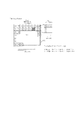
第1の実施の形態におけるデジタル複合機を図1に示す。2000は、本発明の本発明の画像入出力制御装置及び画像処理装置を適用可能なコントローラ(Controller Unit)である。
【0021】
ここで、2150はデジタル複合機全体を制御するシステム制御部である。2149及び2151は入力した画像データに対して所定の画像処理を行う画像処理部であり、その詳細については後述する。2008は画像リングであり、システム処理部2150と画像処理部2149、及び画像処理部2151をリング状に接続する。
【0022】
2012は各種設定や動作指示操作を行うための操作部である。2002はRAMであり、2003はROMである。2143は汎用PCIバスであり、2004は外部記憶装置、2144は、ディスクコントローラである。2050は、公衆回線と接続するためのモデム、2146はPHY/PMDであり、LAN2011と接続しており、デジタル複合機はモデム2050及びPHY/PMDを介して外部機器と通信可能である。画像処理部1(2149)には、プリンタ2095、画像メモリ1及び2(2123)が接続されている。画像処理部2(2151)には、スキャナ2070、第2の画像メモリ1及び2が接続される。
【0023】
ここで、ハードウェアとしての観点から見た、コントローラ2000の構成について説明する。
【0024】
従来から、デジタル複写機等画像入出力装置におけるコントローラは、システムLSIとして半導体基板上に構成されている。特に近年、本実施の形態に対応させると、システム制御部2150及び画像処理部1(2149)及び画像処理部2(2151)等の機能を実現するための回路を、1つの半導体基板上に構成したコントローラが提案されている。
【0025】
しかし、従来とは異なり、本実施の形態では装置の機能変更等に対応できるように、各機能を実現するための回路をそれぞれ異なるユニット、すなわち半導体基板上に構成する。
【0026】
具体的に説明すると、システム制御部2150を1つの半導体基板上に構成し、画像処理部1(2149)及び画像処理部2(2151)を、それぞれ1つの半導体基板上に構成している。
【0027】
また、ここで述べる半導体基板は、ICチップと言い換えることできる。すなわち、本実施形態では、コントローラ2000が1つのプリント基板であり、このプリント基板上に、システム制御部2150、画像処理部1(2149)、画像処理部2(2151)がICチップとして実装されている。
【0028】
なお、本発明はこれに限るものではなく、例えば、システム制御部2150、画像処理部1(2149)、画像処理部2(2151)が、それぞれ別々のプリント基板上にICチップとして実装されていてもよい。
【0029】
次に、システム制御部2150及び画像処理部1(2149)の内部構成を説明するための詳細な全体構成を図2に示す。なお、図2では、画像処理部1(2149)の内部構成のみを示しているが、画像処理部2(2151)は、画像処理部1(2149)と同一の構成を有するものとし、以下、特に断らない限り、同一の符号を用いて説明する。
【0030】
コントローラ2000は、画像入力デバイスであるスキャナ2070や画像出力デバイスであるプリンタ2095と接続し、一方ではLAN2011や公衆回線WAN2051と接続することで、画像情報やデバイス情報の入出力、PDLデータのイメージ展開を行う為のコントローラである。
【0031】
CPU2001はシステム全体を制御するプロセッサである。本実施の形態では2つのCPUを用いた例を示す。これら二つのCPUは、共通のCPUバス2126に接続され、さらに、システムバスブリッジ2007に接続される。
【0032】
システムバスブリッジ2007は、バススイッチであり、CPUバス2126、RAMコントローラ2124、ROMコントローラ2125、IOバス1(2127)、IOバス2(2129)、画像リングインターフェース1(2147)、画像リングインターフェース2(2148)が接続される。
【0033】
RAM2002は、CPU2001が動作するためのシステムワークメモリであり、画像データを一時記憶するための画像メモリでもある。RAM2002は、RAMコントローラ2124により制御される。
【0034】
ROM2003はブートROMであり、システムのブートプログラムが格納されている。ROMコントローラ2125により制御される。
【0035】
IOバス1(2127)は、内部IOバスの一種であり、標準バスであるUSBバスのコントローラ、USBインターフェース2138、汎用シリアルポート2139、インタラプトコントローラ2140、GPIOインターフェース2141が接続される。IOバス1(2127)には、バスアービタ(図示せず)が含まれる。
【0036】
操作部I/F2006は操作部UI2012とのインターフェース部で、操作部2016に表示する画像データを操作部2012に対して出力する。また、操作部2012から本システム使用者が入力した情報を、CPU2001に伝える役割をする。
【0037】
IOバス2(2129)は内部IOバスの一種であり、汎用バスインターフェース1及び2(2142)と、LANコントローラ2010が接続される。IOバス2(2142)にはバスアービタ(図示せず)が含まれる。
【0038】
汎用バスインターフェース1と2(2142)は、2つの同一のバスインターフェースから成り、標準IOバスをサポートするバスブリッジである。本実施の形態では、PCIバス(2143)を採用した例を示した。
【0039】
HDD2004はハードディスクドライブで、システムソフトウェア、画像データを格納する。ディスクコントローラ2144を介して一方のPCIバス2143に接続される。
【0040】
LANコントローラ2010は、MAC回路2145、PHY/PMD回路2146を介しLAN2011に接続し、情報の入出力を行う。Modem2050は公衆回線2051に接続し、情報の入出力を行う。
【0041】
パケット転送手段である画像リングインターフェース1(2147)及び画像リングインターフェース2(2148)は、システムバスブリッジ2007と画像データを高速で転送する画像リング2008を接続し、タイル化されたデータをRAM2002と画像処理部2149間で転送するDMAコントローラである。
【0042】
同じくパケット転送手段である画像リング2008は、一連の単方向接続経路の組み合わせにより構成される。画像リング2008は、画像処理部1(2149)内で、画像リングインターフェース3(2101)、及び画像リングインターフェース4(2102)を介し、コマンド処理部2104、ステータス処理部2105、タイルバス2127に接続される。
【0043】
コマンド処理部2104は、画像リングインターフェースへの接続に加え、レジスタ設定バス2109に接続され、画像リングを介して入力したCPU2001より発行されたレジスタ設定要求を、レジスタ設定バス2109に接続される該当ブロックへ書き込む。また、CPU2001より発行されたレジスタ読み出し要求に基づき、レジスタ設定バスを介して該当レジスタより情報を読み出し、画像リングインターフェース4(2102)に転送する。
【0044】
ステータス処理部2105は各画像処理部の情報を監視し、CPU2001に対してインタラプトを発行するためのインタラプトバケットを生成し、画像リングインターフェース4(2102)に出力する。
【0045】
タイルバス2107には上記ブロックに加え、画像入力インターフェース2112、画像出力インターフェース2113、複数の矩形画像処理部2116〜2119、2030等の機能ブロックが接続される。
【0046】
本実施の形態では、矩形画像処理部として、多値化部2119、2値化部2118、色空間変換部2117、画像回転部2030、解像度変換部2116を実装している。
【0047】
なお、図1においては画像処理部2(2151)にあるべきスキャナ2070を、図面を簡単化するために、ここでは画像処理部1(2149)に接続した構成で説明している。
【0048】
画像処理部2(2151)内の、画像入力インターフェース2112は、後述するスキャナ2170により補正画像処理されたラスタイメージデータを入力とし、レジスタ設定バスを介して設定された、所定の方法により矩形データへの構造変換とクロックの同期化を行い、タイルバス2107に対し出力を行う。
【0049】
画像処理部1(2149)内の画像出力インターフェース(2113)は、タイルバス2107からの矩形データを入力とし、ラスター画像への構造変換及び、クロックレートの変更を行い、ラスター画像をプリンタ2095へ出力する。
【0050】
画像処理部1(2149)の画像入力インターフェース、画像処理部2(2151)の画像出力インターフェースは本実施の形態では使用しない。
【0051】
画像回転部2030は画像データの回転を行う。解像度変換部2116は画像の解像度の変更を行う。色空間変換部2117はカラー及びグレースケール画像の色空間の変換を行う。2値化部2118は、多値カラー、グレースケール画像を2値化する。多値化部2119は2値画像を多値データへ変換する。
【0052】
メモリ制御部2122は、メモリバス2108に接続され、各画像処理部の要求に従い、あらかじめ設定されたアドレス分割により、画像メモリ1及び画像メモリ2(2123)に対して、画像データの書き込み、読み出し、必要に応じてリフレッシュ等の動作を行う。本実施の形態では、画像メモリにSDRAMを用いるものとする。
【0053】
次に、本実施の形態におけるデジタル複合機を含むネットワークシステム全体の構成図を図3に示す。
【0054】
1001は上述した本実施の形態におけるデジタル複合機であり、本発明の画像出力制御装置及び画像処理装置を適用可能なコントローラにより制御されている。
【0055】
デジタル複合機1001は、スキャナとプリンタから構成され、スキャナから読み込んだ画像をローカルエリアネットワーク1010(以下LAN)に流したり、LANから受信した画像をプリンタによりプリントアウトできる。
【0056】
また、スキャナから読んだ画像を図示しないFAX送信手段により、PSTNまたはISDN1030に送信したり、PSTNまたはISDNから受信した画像をプリンタによりプリントアウトできる。1002は、データベースサーバで、デジタル複合機1001により読み込んだ2値画像及び多値画像をデータベースとして管理する。
【0057】
1003は、データベースサーバ1002のデータベースクライアントで、データベース1002に保存されている画像データの閲覧/検索等ができる。
【0058】
1004は、電子メールサーバで、デジタル複合機1001により読み取った画像を電子メールの添付として受け取ることができる。1005は、電子メールのクライアントで、電子メールサーバ1004の受け取ったメールを受信し閲覧したり、電子メールを送信したりすることが可能である。
【0059】
1006がHTML文書をLANに提供するWWWサーバで、デジタル複合機1001によりWWWサーバで提供されるHTML文書をプリントアウトできる。
【0060】
1011は、ルータでLAN1010をインターネット/イントラネット1012と連結する。インターネット/イントラネットに、前述したデータベースサーバ1002、WWWサーバ1006、電子メールサーバ1004、デジタル複合機1001と同様の装置が、それぞれ1020,1021,1022,1023として連結している。一方、デジタル複合機1001は、PSTNまたはISDN1030を介して、FAX装置1031と送受信可能になっている。
【0061】
また、LAN上にプリンタ1040も連結されており、デジタル複合機1001により読み取った画像をプリントアウト可能なように構成されている。
【0062】
次に、本発明の画像入出力制御装置及び画像処理装置を適用可能なコントローラ2000内で処理されるパケットデータのパケットフォーマットについて説明する。
【0063】
本実施の形態におけるコントローラ2000内では、画像データ、CPU2001によるコマンド、各ブロックより発行される割り込み情報等を、パケット化された形式で転送する。本実施の形態では、図4に示すデータパケット、図6に示すコマンドパケット、図7に示すインタラプトパケットの3種の異なる種類のパケットが使用される。
【0064】
まず、図4を用いてデータパケットについて説明する。本実施の形態では画像データを32pixel x 32pixelのタイル(Tile)単位の画像データ(ImageData+padding)3002に分割して取り扱う例を示した。
【0065】
このタイル単位の画像に、必要なヘッダ情報(header)3001及び画像付加情報等(Zdata+padding)3003を付加してデータパケット(DataPacket)とする。以下にヘッダ情報3001に含まれる情報について説明を行う。
【0066】
パケットのタイプはヘッダ情報3001内のパケットタイプ(PcktType)3004で区別される。チップID(ChipID)3005はパケットを送信するターゲットとなるチップのIDを示す。データタイプ(DataType)3006ではデータのタイプを示す。ページID(PageID)3007はページを示しており、ジョブID(JobID)3008はソフトウェアで管理するためのIDを格納する。
【0067】
タイルの番号はY方向のタイル座標3009とX方向のタイル座標3010の組み合わせで、YnXnで表される。データパケットは画像データが圧縮されている場合と非圧縮の場合がある。本実施形態では非圧縮の場合を示した。圧縮されている場合と非圧縮の場合との区別は圧縮フラグ(CompressFlag)3017で示される。
【0068】
プロセスインストラクション(Process Instruction)3011は左詰で処理順に設定し、各処理ユニット(上述の矩形画像処理部等)は、処理後プロセスインストラクション3011を左に8ビットシフトする。プロセスインストラクション3011はユニットID(UnitID)3019とモード(Mode)3020の組が8組格納されている。ユニットID3019は各処理ユニットを指定し、モード3020は各処理ユニットでの動作モードを指定する。これにより、1つのパケットは8つのユニットで連続して処理することができる。
【0069】
パケット長(PacketByteLength)3012はパケットのトータルバイト数を示す。画像データ長(ImageDataByteLengh)3015は画像データのバイト数、Zデータ長(ZdataByteLength)3016は画像付加情報のバイト数を表し、画像データオフセット(ImageDataOffset)3013、Zデータオフセット(ZdataOffset)3014は、それぞれのデータのパケットの先頭からのオフセットを表している。
【0070】
次に、図5を用いてパケットテーブル(Packet Table)について説明する。各パケットはパケットテーブル6001によって管理する。パケットテーブル6001の構成要素は次の通りで、それぞれテーブルの値に0を5bit付加すると、パケットの先頭アドレス(PacketAddressPointer)6002、パケット長(Byte Length)6005となる。またここで、Packet Address Pointer 27bit + 5b00000 = パケット先頭アドレス、Packet Length 11bit + 5b00000 = パケット長の関係が成り立つ。パケットテーブル6001とチェーンテーブル(ChainTable)6010は分割されないものとする。
【0071】
パケットテーブル6001は常に走査方向に並んでおり、Yn/Xn=000/000, 000/001,000/002,....という順で並んでいる。このパケットテーブル6001のEエントリは一意にひとつのタイルを示す。また、Yn/Xmaxの次のエントリはYn+1/X0となる。
【0072】
パケットがひとつ前のパケットとまったく同じ データである場合は、そのパケットはメモリ上には書かず、パケットテーブルのエントリに1つめのエントリと同じ先頭アドレス(PacketAddressPointer)、パケット長(PacketLength)を格納する。1つのパケットデータを2つのテーブルエントリが指すようなかたちになる。この場合、2つめのテーブルエントリのリピートフラグ(RepeatFlag)6003がセットされる。
【0073】
パケットがチェーンDMAにより複数に分断された場合は、分割フラグ(DivideFlag)6004をセットし、そのパケットの先頭部分が入っているチェーンブロックのチェーンテーブル番号(ChainTableNo)6006をセットする。
【0074】
チェーンテーブル6010のエントリはチェーンブロックアドレス(ChainBlockAddress)6011とチェーンブロック長(ChainBlockLength)6012からなっており、テーブルの最後のエントリにはアドレス、データ長共に0を格納しておく。
【0075】
次に、図6を用いてコマンドパケット(Command Packet)について説明する。
【0076】
コマンドパケットはレジスタ設定バス2109へのアクセスを行うためのものである。コマンドパケットを用いることにより、CPU2001より画像メモリ2123へのアクセスも可能である。
【0077】
チップID(ChipID)4004にはコマンドパケットの送信先となる画像処理部を表すIDが格納される。ページID(PageID)4007、ジョブID(JobID)4008はソフトウェアで管理するためのページIDとジョブIDを格納する。
【0078】
パケットID(PacketID)4009は1次元で表される。従って、データパケット(Data Packet)のX座標(X-coordinate)4009のみを使用する。パケット長(PacketByteLength)4010は128Byte固定である。
【0079】
パケットデータ部(Command)4002には、アドレス(Address)4011とデータ(Data)4012の組を1つのコマンドとして、最大12個のコマンドを格納することが可能である。ライトかリードかのコマンドのタイプは、コマンドタイプ(CmdType)4005で示され、コマンドの数はコマンド数(Cmdnum)4006で示される。
【0080】
最後に、図7を用いてインタラプトパケット(Interrupt Packet)について説明する。
【0081】
インタラプトパケットは画像処理部からCPU2001への割り込みを通知するためのものである。ステータス処理部2105はインタラプトパケットを送信すると、次に送信の許可がされるまではインタラプトパケットを送信してはならない。
【0082】
パケット長(PacketByteLength)5006は128Byte固定である。パケットデータ部(IntData)5002には、画像処理部の各内部モジュール(各矩形画像処理部、入出力インターフェイス等)のステータス情報(ModuleStatus)5007が格納されている。ステータス処理部2105は画像処理部内の各モジュールのステータス情報を集め、一括してシステム制御部2150に送ることができる。
【0083】
チップID(ChipID)5004にはインタラプトパケットの送信先となるシステム制御部2150を表すIDが、また、インタラプトチップID(IntChipID)5005にはインタラプトの送信元となる画像処理部を表すIDが格納される。
【0084】
以下、コントローラ2000が行う典型的な処理として、ユーザーが操作部2012よりコピージョブの指示を行った場合の処理を、図8、図9に示すフローチャートを用いて説明する。
【0085】
まず、コントローラ2000がコピージョブを受け、スキャナ2070を用いたスキャン動作を開始し終了するまでの処理を図8を用いて説明する。
【0086】
CPU2001は、操作部インターフェース2006より情報の伝達を受け、紙サイズ等の情報より、画像リングインターフェース2(2148)に、転送パケット数、RAM2002上での画像格納アドレス等の必要情報をプログラムする(S801)。
【0087】
CPU2001はレジスタアクセスリング2137を介し、画像リングインターフェース1(2147)内部にあるコマンドパケット生成レジスタをプログラミングし、画像入力インターフェース2112へ、紙サイズ、色空間情報等、必要情報を設定するための、コマンドパケットを生成する。この場合、コマンドパケットのチップID4004を画像処理部2(2151)を示す“2”に設定する(S802)。
【0088】
その後、画像リングインターフェイス1(2147)は、コマンドパケットを画像リング2008を介して画像処理部1(2149)へ転送する(S803)。
【0089】
画像処理部1(2149)の画像リングインターフェース3(2101)は、コマンドパケットのチップIDを検査する。ここで、チップIDは、自チップのIDである“1”ではないので、画像リングインターフェース4(2102)にコマンドパケットを転送する(S804)。
【0090】
画像リングインターフェース4(2102)は、再び、画像リング2008を介し、コマンドパケットを画像処理部2(2151)に転送する(S805)。
【0091】
画像処理部2(2151)に到達したコマンドパケットは、画像処理部2内の画像リングインターフェース3(2101)において、コマンドパケットのチップIDが検査される。ここで、コマンドパケットのチップIDと、自チップのIDが“2”で一致する。この場合、コマンド処理部(2104)はコマンドパケットのコマンドデータ及びヘッダの情報に基づき、レジスタ設定バス(2109)を介し画像入力インターフェース2112をプログラムする(S806)。
【0092】
続いて、同様に、CPU2001はコマンドパケットを用い、画像入力インターフェース2112内部のスキャナ通信インターフェースをプログラミングし、スキャナ2070に対し、スキャンの開始を指示する(S807)。
【0093】
スキャナ2070より入力された画像情報は画像入力インターフェース2112、及びメモリバス2108を介し、メモリ制御部2122により制御される画像メモリ2123に一旦格納される(S808)。
【0094】
格納された画像データは、再び画像入力インターフェース2112により、32×32画素ごとに読み出され、パケットタイプ(PcktType)3004、チップID(ChipID)3005、データタイプ(DataType)3006、ページID(PageID)3007、ジョブID(Job ID)3008、Y方向のタイル座標(PacketIDYcoordinate)3009、X方向のタイル座標(PacketIDXcoordinate)3010、圧縮フラグ(CompressFlag)3017、プロセスインストラクション(Process Instruction)3011、パケットのデータ長(PacketByteLength)3012等のヘッダ情報を画像データに付加してデータパケットを生成し、生成したデータパケットをタイルバス2107に出力する(S809)。
【0095】
上記データパケットは順次作成され、コマンドパケットと同様に、チップIDに基づき画像リングインターフェース4(2102)、画像リング2008、画像リングインターフェース2(2148)を介し画像リングインターフェース2(2148)に転送される。そして画像リングインターフェース2(2148)にプログラミングされた情報に基づき、RAM2002に順次格納される。画像リングインターフェース2(2148)は同時に、パケットテーブル6001をRAM2002上に作成する(S810)。
【0096】
1ページのスキャン動作が終了すると、スキャナ通信手段を用い、画像入力インターフェースに終了が伝達される。画像入力インターフェース2112は、割り込み信号(図示せず)を用い、ステータス処理部2105に割り込みを通知する(S811)。
【0097】
画像処理部2(2151)内のステータス処理部2105はインタラプトパケット(図7)を作成し、画像リングインタフェース2(2148)へ転送する(S812)。
【0098】
画像リングインターフェース2148はインタラプトパケットを解釈し、インタラプト信号(図示せず)により、インタラプトをインタラプトコントローラ2140へ伝達する。インタラプトは、インタラプトコントローラ2140より、CPU2001に伝達され、CPU2001はスキャン動作の終了を検出する(S813)。
【0099】
スキャン動作を終了すると、プリンタ2095を用いたプリント動作を開始する。プリント動作におけるコントローラ2000の処理について図9を用いて説明する。
【0100】
CPU2001はレジスタアクセスリング2137を介し、チップID“1”を有するコマンドパケットを作成する(S901)。
【0101】
そして、作成したコマンドパケットを画像リングインターフェース1(2147)より、画像リング2008を介して画像処理部1(2149)に転送する(S902)。
【0102】
画像処理部1(2149)の画像リングインターフェース3(2101)は、入力したコマンドパケットを検査する。ここで、チップIDが“1”であるので、コマンドパケットのコマンドデータに基づき、コマンド処理部2104、レジスタ設定バス2109を介し、画像処理部1(2149)内の画像出力インターフェース(2113)へ画像出力処理のための必要情報の設定を行う(S903)。
【0103】
CPU2001は同様に、コマンドパケットを使用し、画像処理部1内の画像出力インターフェース2113に備えられたプリンタ通信手段により、プリンタ2095に印字待機を指示する(S904)。
【0104】
続いて、CPU2001は画像リングインターフェース1(2147)内に備えられたDMA手段に、パケットテーブルの存在するメモリアドレス等をプログラムする(S905)。
【0105】
画像リングインターフェース1(2147)内のDMAは、プログラムされた情報に基づき、RAM2002内より、データパケットを読み出しチップID“1”をヘッダに付加したデータパケットを生成する(S906)。
【0106】
そして、画像リングインターフェース1(2147)内のDMAは、生成したデータパケットを画像リング2008を介し、画像処理部1(2149)に転送する(S907)。
【0107】
画像処理部1(2149)の画像リングインターフェース3(2101)は、入力したデータパケットを検査する。ここで、チップIDが“1”であるので、画像リングインターフェース3(2101)、タイルバス(2107)を介し、順次画像出力インターフェース2113へ転送する(S908)。
【0108】
画像出力インターフェース2113は、受け取ったデータパケットより、画像部分を抽出し、画像データを画像メモリ2123へ格納する(S909)。
【0109】
必要画素分画像データが画像メモリ2123に蓄積された時点で、画像出力インターフェース2113は画像データを画像メモリ2123より順次読み出し、プリンタ2095に出力する(S910)。
【0110】
結果、ユーザーは、コピー結果である画像プリントを得る。画像出力が必要画素数終了した時点で、スキャン動作の場合と同様に、インタラプトパケットにより、終了割り込みがCPU2001に伝達される(S911)。
【0111】
以上、スキャナ2070及び画像処理部2(2151)を用いたスキャン動作、プリンタ2095と画像処理部1(2095)を用いたプリント動作を組み合わせたコピー動作を説明した。
【0112】
この説明から明らかなように、複数ページコピーの場合には、プリント動作とスキャン動作が同時に発生するが、画像リング2008はスキャンデータパケットとプリントデータパケットが同一のバスを通過することはない。
【0113】
そして、画像リング2008は、単方向接続経路の組み合わせにより構成されており、バスの競合等による処理速度の低下を起こすことなく、低コストな転送手段を構成することができる。
【0114】
また、解像度変換部2116、画像回転2030等の矩形画像処理部は、スキャン動作とプリント動作で用いられ、スキャン等動作における画像データの処理と、プリント動作における画像データの処理が競合してしまうことがある。
【0115】
しかし、本実施の形態におけるコントローラの構成をとることで、競合した場合も画像処理部1、画像処理部2のそれぞれの解像度変換部、画像回転部が利用でき、競合による速度低下が起こらない。
【0116】
以上説明してきたように、本実施の形態によれば、デジタル複合機のコントローラにおいて、システム制御部を構成する半導体基板と、画像処理部1を構成する半導体基板と、画像処理部2を構成する半導体基板とを、それぞれ別々の基板とし、それぞれの間は画像リングにより接続し、パケットデータによるデータ転送を行うようにした。
【0117】
これにより、機能の変更や追加等が生じた場合においても、容易にコントローラの構成を変更することができる。また、画像リングによる単方向のデータ転送を行うので、にバス制御等のための部品点数を増やすことなく、バスの競合による処理速度の低下を少なくすることができる。
【0118】
また、上述のリング状に接続されたシステム制御部と各画像処理部との間でのコマンドのやり取りに、各画像処理部における画像処理や画像入出力処理、接続された外部装置の動作処理設定等を行うためのコマンドデータに、どの画像処理部において処理設定を行うかを識別するためのチップIDを含むヘッダを付加したコマンドパケットを用いた。
【0119】
これにより、システム制御部は各画像処理部に対して別々の処理設定を容易に行うことができるので、システム制御部の負荷を増加させることなく、平行処理等における画像処理部の競合を回避することができる。
【0120】
また、画像処理部2において、コマンドパケットによる設定に基づき、スキャナにより入力した画像データをシステム制御部に送信し、システム制御部において、画像処理部2から受信した画像データをRAMに記憶し、1ページ分の画像データをRAMに記憶した後、RAMの画像データを画像処理部1に送信し、画像処理部1において、コマンドパケットによる設定に基づき、システム制御部から受信した画像データをプリンタに出力するようにした。
【0121】
このデータ転送処理を単方向バスである画像リングを用いて行うことで、画像処理部やバスの競合等による処理速度の低下を起こすことなく、コピー処理を行うことができる。
【0122】
同様に、上述のリング状に接続されたシステム制御部と各画像処理部との間での画像データのやり取りに、所定の大きさを持つ矩形単位に分割された画像データにどの画像処理部において処理設定を行うかを識別するためのチップIDを含むヘッダを付加したコマンドパケットを用いた。
【0123】
これにより、矩形画像データ単位で画像処理を行う画像処理部を指定することができ、複数機能動作を行う際に画像処理部内の矩形画像処理部を用いた画像処理の競合が起こることを避けることができる。
【0124】
(第2の実施形態)
本実施形態では、第1の実施形態で説明したコントローラに、さらにもう1つ画像処理部を追加する。本実施形態におけるデジタル複合機を図10に示す。
【0125】
図10に示されるように、本実施形態では、画像処理部3(2152)が新しく追加されている。ここで、第1の実施形態と同様に、システム制御部2150を1つの半導体基板上に構成し、画像処理部1(2149)、画像処理部2(2151)、及び画像処理部3(2152)を、それぞれ1つの半導体基板上に構成している。
【0126】
図10のデジタル複合機において、2000は、本発明の本発明の画像入出力制御装置及び画像処理装置を適用可能なコントローラ(Controller Unit)である。ここで、2150はデジタル複合機全体を制御するシステム制御部である。
【0127】
2149,2151及び2152は入力した画像データに対して所定の画像処理を行う画像処理部であり、その詳細については後述する。2008は画像リングであり、システム処理部2150と画像処理部2149,2151及び2152をリング状に接続する。
【0128】
次に、画像処理部1(2149)の内部構成を説明するための詳細な全体構成を図11に示す。
【0129】
パケット転送手段である画像リング2008は、一連の単方向接続経路の組み合わせにより構成される。画像リング2008は、画像処理部2149内で、画像リングインターフェース3(2101)、及び画像リングインターフェース4(2102)を介し、コマンド処理部2104、ステータス処理部2105、タイルバス2107に接続される。
【0130】
タイルバス2107には上記ブロックに加え、画像出力インターフェース2113が接続される。
【0131】
画像処理部1(2149)内の画像出力インターフェース2113は、タイルバス2107からの矩形データを入力とし、ラスター画像への構造変換及び、クロックレートの変更を行い、ラスター画像をプリンタ2195へ出力する。
【0132】
メモリ制御部2122は、メモリバス2108に接続され、画像出力インターフェース2113の要求に従い、画像メモリ1(2113)に対して、画像データの書き込み、読み出し、必要に応じてリフレッシュ等の動作を行う。本実施の形態では、画像メモリにSDRAMを用いた例を示した。
【0133】
次に、画像処理部2(2151)の内部構成を説明するための詳細な全体構成を図12に示す。
【0134】
パケット転送手段である画像リング2008は、一連の単方向接続経路の組み合わせにより構成される。画像リング2008は、画像処理部2(2151)内で、画像リングインターフェース3(2101)、及び画像リングインターフェース4(2102)を介し、コマンド処理部2104、ステータス処理部2105、タイルバス2107に接続される。この構成は、画像処理部1(2149)と同等である。
【0135】
タイルバス2107には上記ブロックに加え、画像入力インターフェース2112が接続される。
【0136】
画像処理部2(2151)内の画像入力インターフェース2112は、スキャナ2070からのラスタデータを入力とし、矩形画像への構造変換及び、クロックレートの変更を行い、矩形画像をタイルバス2107へ出力する。
【0137】
メモリ制御部2122は、メモリバス2108に接続され、画像入力インターフェース2112の要求に従い、画像メモリ1(2123)に対して、画像データの書き込み、読み出し、必要に応じてリフレッシュ等の動作を行う。本実施の形態では、画像メモリにSDRAMを用いた例を示した。
【0138】
次に、画像処理部3(2152)の内部構成を説明するための詳細な全体構成を図13に示す。
【0139】
パケット転送手段である画像リング2008は、一連の単方向接続経路の組み合わせにより構成される。画像リング2008は、画像処理部3(2152)内で、画像リングインターフェース3(2101)、及び画像リングインターフェース4(2102)を介し、コマンド処理部2104、ステータス処理部2105、タイルバス2107に接続される。この構成は、画像処理部1,2と同等である。
【0140】
タイルバス2107には上記ブロックに加え、解像度変換部2116が接続される。
【0141】
解像度変換部2116は、画像リング2008から入力された画像パケットデータをタイルバス2107を介し受け取り、メモリバス2108を介し画像メモリ2123を用いて矩形データをラスタデータに変換した後に、解像度変換を行い、生成された画像データを再びメモリバス2108、画像メモリ2123を用いて、矩形データに変換する。その後、タイルバス2107を介し矩形データを画像リングインターフェース4(2102)に出力する。画像リングインターフェース4(2102)は、矩形データを画像パケットデータとして画像リング2008に送出する。
【0142】
以下、コントローラ2000が行う典型的な処理として、ユーザーが操作部2012より変倍コピージョブの指示を行った場合の処理を例に図14,15,及び16に示すフローチャートを用いて説明する。
【0143】
まず、コントローラ2000がコピージョブを受け、スキャナ2070を用いたスキャン動作を開始し、スキャン画像の解像度を変換し、解像度変換されたスキャン画像をRAM2002に格納し終るまでの処理を図13、14を用いて説明する。
【0144】
CPU2001は、操作部インターフェース2006より情報の伝達を受け、紙サイズ等の情報より、画像リングインターフェース2(2148)に、転送パケット数、RAM2002上での画像格納アドレス等の必要情報をプログラムする(S1401)。
【0145】
CPU2001はレジスタアクセスリング2137を介し、画像リングインターフェース1(2147)内部にあるコマンドパケット生成レジスタをプログラミングし、画像入力インターフェース2112における、紙サイズ、色空間情報等、必要情報を設定するための、コマンドパケットを生成する。この場合、コマンドパケットのチップID4004を画像処理部2(2151)を示す“2”に設定する(S1402)。
【0146】
その後、画像リングインターフェース1(2147)は、コマンドパケットを画像リング2008を介して画像処理部1(2149)へ転送する(S1403)。
【0147】
画像処理部1(2149)の画像リングインターフェース3(2101)は、コマンドパケットのチップIDを検査し、自チップのIDである“1”ではないので、画像リングインターフェース4(2102)にコマンドパケットを転送する(S1404)。
【0148】
画像リングインターフェース4(2102)においてもチップIDが異なるので、再び、画像リングインターフェース4(2102)は、画像リング2008を介し、コマンドパケットを画像処理部2(2151)に転送する(S1405)。
【0149】
画像処理部2(2151)に到達したコマンドパケットは、画像処理部2内の画像リングインターフェース3(2101)において、コマンドパケットのチップIDが検査される。ここで、コマンドパケットのチップIDと、自チップのIDが“2”で一致する。この場合、コマンド処理部2104はコマンドパケットのコマンドデータ及びヘッダの情報に基づき、レジスタ設定バス2109を介し画像入力インターフェース2112をプログラムする(S1406)。
【0150】
続いてCPU2001は、操作部インターフェース2006より情報の伝達を受け、変倍の解像度を算出し、画像リングインターフェース2(2148)に、変換解像度等、解像度変換情報をプログラムする(S1407)。
【0151】
CPU2001はレジスタアクセスリング2137を介し、画像リングインターフェース1(2147)内部にあるコマンドパケット生成レジスタをプログラミングし、画像処理部3(2151)の解像度変換部2116における変換解像度を設定するための、コマンドパケットを生成する。この場合、コマンドパケットのチップID4004を画像処理部3(2151)を示す“3”に設定する(S1408)。
【0152】
その後、画像リングインターフェース1(2147)は、コマンドパケットを画像リング2008を介して画像処理部1(2149)へ転送する(S1409)。
【0153】
画像処理部1(2149)の画像リングインターフェース3(2101)は、コマンドパケットのチップIDを検査し、自チップのIDである“1”ではないので、画像リングインターフェース4(2102)にコマンドパケットを転送する(S1410)。
【0154】
画像処理部1(2149)の画像リングインターフェース4(2102)においてもチップIDが異なるので、再び、画像リングインターフェース4(2102)は、画像リング2008を介し、コマンドパケットを画像処理部2(2151)に転送する(S1411)。
【0155】
画像処理部2(2149)の画像リングインターフェース3(2101)は、コマンドパケットのチップIDを検査し、自チップのIDである“2”ではないので、画像リングインターフェース4(2102)にコマンドパケットを転送する(S1412)。
【0156】
画像処理部2(2151)の画像リングインターフェース4(2102)においてもチップIDが異なるので、再び、画像リングインターフェース4(2102)は、画像リング2008を介し、コマンドパケットを画像処理部3(2152)に転送する(S1413)。
【0157】
画像処理部3(2152)に到達したコマンドパケットは、画像処理部3内の画像リングインターフェース3(2101)において、コマンドパケットのチップIDが検査される。ここで、コマンドパケットのチップIDと、自チップのIDが“3”で一致する。この場合、コマンド処理部(2104)はコマンドパケットのコマンドデータ及びヘッダの情報に基づき、レジスタ設定バス(2109)を介し解像度変換部2116をプログラムする(S1414)。
【0158】
続いて、同様に、CPU2001はコマンドパケットを用い、画像入力インターフェース2112内部のスキャナ通信インターフェースをプログラミングし、スキャナ2070に対し、スキャンの開始を指示する(S1415)。
【0159】
スキャナ2070より入力された画像情報は画像入力インターフェース2112、及びメモリバス2108を介し、メモリ制御部2122により制御される画像メモリ2123に一旦格納される(S1416)。
【0160】
格納された画像データは、再び画像入力インターフェース2112により、32×32画素ごとに読み出され、パケットタイプ(PcktType)3004、チップID(ChipID)3005、データタイプ(DataType)3006、ページID(PageID)3007、ジョブID(Job ID)3008、Y方向のタイル座標(PacketIDYcoordinate)3009、X方向のタイル座標(PacketIDXcoordinate)3010、圧縮フラグ(CompressFlag)3017、プロセスインストラクション(Process Instruction)3011、パケットのデータ長(PacketByteLength)3012等のヘッダ情報を画像データに付加してパケットデータを生成し、生成したパケットデータをタイルバス2017に出力する(S1417)。この際チップIDは“3”に設定され、プロセスインストラクションは解像度変換を示す値が設定される。
【0161】
上記パケットデータは順次作成され、コマンドパケットと同様に、チップIDに基づき画像リングインターフェース4(2102)、画像リング2008を介して、画像処理部3の画像リングインターフェース3(2101)へ転送される。
【0162】
画像処理部3の画像リングインターフェース3(2101)では、パケットのヘッダ検査し、チップIDが“3”であり、プロセスインストラクションが解像度変換を示すので、パケットデータは画像処理部3内の、解像度変換部2116に転送される。解像度変換部2116では、上記したように、入力されるパケットを順次画像メモリに格納し、ラスタ画像に変換した後に、公知の方法にて、解像度の変換を行い、生成された新しい解像度の画像を矩形に切り出し、再度パケットデータとして、画像リングに送出する(S1418)。
【0163】
そして画像リングインターフェース2(2148)にプログラミングされた情報に基づき、RAM2002に順次格納される。画像リングインターフェース2(2148)は同時に、パケットテーブル6001をRAM2002上に作成する(S1419)。
【0164】
1ページのスキャン動作が終了すると、スキャナ通信手段を用い、画像入力インターフェースに終了が伝達される。画像処理部2(2151)の画像入力インターフェース2112は、割り込み信号(図示せず)を用い、画像処理部2(2151)のステータス処理部2105に割り込みを通知する(S1420)。
【0165】
画像処理部2(2151)内のステータス処理部2105はインタラプトパケット(図5000)を作成し、画像リングインターフェース2(2148)へ転送する(S1421)。
【0166】
画像リングインターフェース2(2148)はインタラプトパケットを解釈し、インタラプト信号(図示せず)により、インタラプトをインタラプトコントローラ2140へ伝達する。インタラプトは、インタラプトコントローラ2140より、CPU2001に伝達され、CPU2001はスキャン動作の終了を検出する(S1422)。
【0167】
スキャン動作を終了すると、プリンタ2095を用いたプリント動作を開始する。プリント動作におけるコントローラ2000の処理について図16を用いて説明する。
【0168】
CPU2001はレジスタアクセスリング2137を介し、チップID“1”を有するコマンドパケットを作成する(S1601)。
【0169】
そして、作成したコマンドパケットを画像リングインターフェース1(2147)より、画像リング2008を介して画像処理部1(2149)に転送する(S1602)。
【0170】
画像処理部1(2149)の画像リングインターフェース3(2101)は、入力したコマンドパケットを検査する。ここで、チップIDが“1”であるので、コマンドパケットのコマンドデータに基づき、コマンド処理部2104、レジスタ設定バス2109を介し、画像処理部1(2149)内の画像出力インターフェース2113へ画像出力処理のための必要情報の設定を行う(S1603)。
【0171】
CPU2001は同様に、コマンドパケットを使用し、画像処理部1(2149)内の画像出力インターフェース2113に備えられたプリンタ通信手段により、プリンタ2095に印字待機を指示する(S1604)。
【0172】
続いて、CPU2001は画像リングインターフェース1(2147)内に備えられたDMA手段に、パケットテーブルの存在するメモリアドレス等をプログラムする(S1605)。
【0173】
画像リングインターフェース1(2147)内のDMAは、プログラムされた情報に基づき、RAM2002内より、データパケットを読み出しチップID“1”をヘッダに付加したデータパケットを生成する(S1606)。
【0174】
そして、画像リングインターフェース1(2147)内のDMAは、生成したデータパケットを画像リング2008を介し、画像処理部1(2149)に転送する(S1607)。
【0175】
画像処理部1(2149)の画像リングインターフェース3(2101)は、入力したデータパケットを検査する。ここで、チップIDが“1”であるので、画像リングインターフェース3(2101)、タイルバス2107を介し、順次画像出力インターフェース2113へ転送する(S1608)。
【0176】
画像出力インターフェース2113は、受け取ったデータパケットより、画像部分を抽出し、画像データを画像メモリ2123へ格納する(S1609)。
【0177】
必要画素分画像データが画像メモリ2123に蓄積された時点で、画像出力インターフェース2113は画像データを画像メモリ2133より順次読み出し、プリンタ2095に出力する(S1610)。
【0178】
結果、ユーザーは、コピー結果である画像プリントを得る。画像出力が必要画素数終了した時点で、スキャン動作の場合と同様に、インタラプトパケットにより、終了割り込みがCPU2001に伝達される(S1611)。
【0179】
以上、本実施形態では、システム制御部と画像処理部1、画像処理部1と画像処理部2、画像処理部2と画像処理部3、及び画像処理部3とシステム制御部の間を画像リング2008で接続し、コマンドパケットやデータパケット等の転送を単方向に行うようにした。
【0180】
そして、画像処理部2において、コマンドパケットによる設定情報に基づき、スキャナにより入力した画像データを画像処理部3に送信し、画像処理部3において、コマンドパケットによる設定情報に基づき、画像処理部2から受信した画像データに解像度変換処理を施し、解像度変換処理を施した画像データをシステム制御部に送信し、システム制御部において、画像処理部3から受信した画像データをRAMに記憶する変倍スキャン動作を行なった。
【0181】
そして、システム制御部において、1ページの画像データをRAMに記憶した後、RAMの画像データを画像処理部1に送信し、画像処理部1は、コマンドパケットによる設定情報に基づき、システム制御部から受信した画像データをプリンタに出力するプリント動作を行なった。この変倍スキャン動作とプリント動作の組み合わせで、変倍コピー処理を実現した。
【0182】
このデータ転送処理を単方向バスである画像リングを用いて行うことで、第1の実施形態と同様に、画像処理部やバスの競合等による処理速度の低下を起こすことなく、変倍コピー処理を行うことができる。
【0183】
また、システム制御部と各画像処理部とをそれぞれ別々の半導体基板に構成し、さらに、画像変換処理のための画像処理部3を独立に備えているので、画像変換機能のみの変更や追加等が生じた場合においても、容易にコントローラの構成を変更することができる。
【0184】
例えば、画像処理部3の解像度変換部を、回転処理部、画像合成部等に変更する場合においても、容易に構成を変更することができる。また、プリンタをもう1台接続する場合においても、画像処理部1と画像処理部2の間に画像処理部1と同じ構成の画像処理部を接続するだけでよいので、プリンタの仕様に応じた画像処理部を低コストで供給することができる。
【0185】
(第3の実施形態)
本実施形態におけるコントローラ2000を図17に示す。本実施形態のコントローラ2000において、画像処理部は画像処理部1(2149)のみであり、画像処理部1(2149)の画像リングインターフェース4(2101)が、システム制御部2150の画像リングインターフェース2に接続されている。そして、画像処理部1(2149)にプリンタ2095とスキャナ2070の両方が接続されている。
【0186】
また、画像処理部1(2149)において、タイル伸張部2103とタイル圧縮部2106が追加されている。すなわち、画像リング2008は、画像処理部2149内で、画像リングインターフェース3(2101)、及び画像リングインターフェース4(2102)を介し、コマンド処理部2104、ステータス処理部2105、タイル伸張部(2103)、タイル圧縮部(2106)に接続される。
【0187】
タイル伸張部(2103)は、画像リングインターフェースへの接続に加え、タイルバス(2107)に接続され、画像リングより入力された圧縮後の画像データを伸張し、タイルバス(2107)へ転送するバスブリッジである。本実施形態では、多値データにはJPEG、2値データにはパックビッツを伸張アルゴリズムとして採用した例を示す。
【0188】
タイル圧縮部(2106)は、画像リングインターフェースへの接続に加え、タイルバス(2107)に接続され、タイルバスより入力された圧縮前の画像データを圧縮し、画像リング(2008)へ転送するバスブリッジである。本実施形態では、多値データにはJPEG、2値データにはパックビッツを圧縮アルゴリズムとして採用した例を示す。
【0189】
このように、画像処理部1(2149)が、データパケットを圧縮及び伸張する機能を備えることにより、画像データを記憶する際に必要なRAM2002のデータ容量を削減することができる。
【0190】
圧縮したデータパケットを画像処理部1(2149)からシステム制御部2150へ送信する際には、タイル圧縮部2106において、圧縮後の画像データ長の情報をヘッダに記載し、画像リングインターフェース4(2102)は、ヘッダに画像データ長の情報を含んだデータパケットの送信を行うことになる。
【0191】
しかし、データパケットを圧縮してから送信をする場合、圧縮が終了しないと画像データ長は確定しないため、画像リングインターフェース4(2102)は、圧縮が終了してからパケットを送信しなければならない。すなわち、タイル圧縮部2106等において送信前のデータパケットを保持しておくためのバッファが必要になる。
【0192】
一般に圧縮は圧縮後のデータ容量を予測することは難しく、データによっては元データよりも大きくなってしまう可能性もある。そうなるとバッファの容量は余裕を持たせて確保しておかなければならず、データパケットの最大容量が大きいようなパケットの場合は非常に大きなバッファ容量が必要になってしまうことがある。
【0193】
本実施形態では、圧縮後のパケット画像データを一時保持しておくための大きなバッファが必要でなくなるようにしたコントローラ2000について説明する。
【0194】
まず、図18に、本実施形態におけるタイル画像データを示す。なお、このタイル画像データは、第1及び第2の実施形態におけるタイル画像データとしても用いることができる。
【0195】
図18に示すように、ラスター画像データとしてスキャナ2070等から入力された1ページの原稿1800が、複数の矩形領域(Tile)に分割される。各矩形領域は縦32画素、横32画素の大きさを有しており、各領域毎にタイル画像データが生成される。ここで、A4サイズの原稿をスキャナ2070により600×600dpiの解像度で読み取ったとし、32×32画素のタイルで分割したとすると、A4サイズの原稿から34320個のタイル画像データが生成される。
【0196】
タイル画像生成においては、読み取り解像度や画像処理の都合に応じた設定を行うことで、タイル画像を扱い易い形状や画素数にすることができる。
【0197】
タイルの単位は32×32画素でなくても良く、例えば64×64画素でも良いし、さらには正方形でなく、矩形などでも良い。画像データを圧縮する際は、1ページ分のデータをまとめて圧縮するのではなく、タイル(パケット)毎に画像データだけを圧縮する。
【0198】
図19は本発明における処理に関連するブロックを、図17に示すシステムから抽出した図である。図19を用いて、本実施形態における画像データの流れを説明する。
【0199】
タイルバス2107から非圧縮のデータパケットが入力されると、タイル圧縮部2106はパケットの画像データを圧縮し、圧縮したデータパケットを画像リングインターフェース4(2102)に送る。さらに、画像リングインターフェース4(2102)は、チップID3005を“0”とし、データパケットを画像リング2008に出力する。
【0200】
画像リングインターフェイス2(2148)は、画像リング2008から入力したデータパケットのチップID3005を検査する。ここで、チップIDが、“0”であるので、画像リングインターフェース2(2148)は、システムバスブリッジ2007、RAMコントローラ2124を介してデータパケットをRAM2002に格納する。
【0201】
RAM2002に格納されたデータパケットを出力する時は、画像リングインターフェース1(2147)がシステムバスブリッジ2007を介してRAM2002からデータパケットを読み出す。画像リングインターフェース1(2147)は読み出したデータパケットのチップID3005を“1”とし、データパケットを画像リング2008に出力する。
【0202】
画像リングインターフェース3(2103)は、画像リング2008から入力したデータパケットのチップID3005を検査する。ここで、チップIDが、“1”であるので、画像リングインターフェース2(2148)は、データパケットをタイル伸張部2103に送る。タイル伸張部2103は圧縮されているデータパケットの画像データを解凍し、タイルバス2107へ解凍したデータパケットを送り出す。
【0203】
以上説明した処理において、タイル圧縮部2106がデータパケットのタイル画像データを圧縮し、画像リングインターフェース4(2102)が、圧縮したデータパケットを、画像リング2008を介して、画像リングインターフェース2に送る部分について詳細に説明する。
【0204】
また、ここで、本発明の説明を明確にするために、本実施形態におけるデータパケットのフォーマットは、図4に示すデータパケットにおいて、Zデータ3003を除いたものであるとする。
【0205】
図20はタイル圧縮部2106の内部のブロック図である。2201はパケット入力インターフェースで、入力されたデータパケットを受け取り、受け取ったデータパケットを、ヘッダ3001と画像データ3002に分ける。そして、パケット入力インターフェース2201は、ヘッダ3001を403のパケット出力インターフェースヘ送り、その一方で、画像データ3002を圧縮部2202ヘ送る。
【0206】
圧縮部2202は、入力された画像データ3002を圧縮し、圧縮された画像データ3002を順次パケット出力インターフェース2203ヘ送る。
【0207】
パケット出力インターフェース2203は、パケット入力インターフェース2201から受け取ったヘッダ3001と、圧縮部2202から受け取った画像データ3002を再び合わせてデータパケットを構成し、画像リングインターフェース4(2102)へ送信する。
【0208】
図21に、画像リングインターフェース4(2102)から画像リングインターフェース2(2148)ヘデータパケットを送信する際の信号波形を示す。
【0209】
paketdata[31:0]は、画像リング2008において、パケットのデータが送られる信号で、ヘッダ3001、および画像データ3002の両方がこの信号を使って送られる。
【0210】
信号clk、dataen、sop、eod、eopは、画像リングインターフェース4(2102)により発せられる信号である。
【0211】
dataen信号はパケットを送信するサイクルでアサートされ、そのアサートされているサイクルにおいてパケットが送信される。
【0212】
sop信号はデータパケット送信の開始を示す。sop信号がアサートされているサイクルのpaketdata[31:0]にヘッダ3001が含まれる。
【0213】
画像リングインターフェース4(2102)は、まず、ヘッダ3001を送信する。この時、ヘッダ3001に含まれるパケット長(PacketByteLength)3012及び画像データ長(ImageDataByteLengh)3015は、圧縮がすべて終了するまで確定しないので、未確定のままでよい。例えば0レングスとして送信しても良い。このヘッダ情報は後でフッタによって書き換えられる。
【0214】
次に、画像リングインターフェース4(2102)は、圧縮された画像データ3002をタイル圧縮部2106から受け取り、送信準備が出来次第、順次、画像データ3002を送信していく。図21では、1つの画像データ3002を、5つのデータブロックに分割して送信する例を示している。
【0215】
最後の画像データ3002を送信する際にはeod信号をアサートして、送信を行う。これにより、画像データ3002の最後を画像リングインターフェース2(2148)に通知する。その後、画像リングインターフェース4(2102)は、eop信号をアサートして、確定したパケット長(PacketByteLength)3012及び画像データ長(ImageDataByteLengh)3015を含んだヘッダ3001をフッタとして送信する。
【0216】
画像リングインターフェース2(2148)は、画像リング2008を介して受け取ったデータパケットをRAM2002のあらかじめ設定されたアドレスヘ格納していく。この時、ヘッダ3001を格納したアドレスを内部レジスタなどに保存しておく。この時点では、ヘッダ3001のパケット長(PacketByteLength)3012及び画像データ長(ImageDataByteLengh)3015には未確定な値が書き込まれている。
【0217】
データパケットの最後にフッタを受け取った場合は、ヘッダ3001を格納したアドレスに対してフッタの内容を上書きする。こうすることによりRAM2002上には図4に示したパケットフォーマットに従ったパケット長(PacketByteLength)3012及び画像データ長(ImageDataByteLengh)3015の確定したパケットが作成される。
【0218】
次に、画像データ3002を圧縮しないでRAM2002にデータパケットを格納する場合を考える。
【0219】
タイル圧縮部2106には、圧縮を行うモードと行わないモードの2種類のモードが用意されている。これはCPU2001などからあらかじめモード設定が行なわれる。
【0220】
圧縮を行うモードを設定した場合は、上述したように、画像リングインターフェース4(2102)は、前記受信側であるシステム制御部2150に対して、フッタを送信する情報を転送し、データパケットを送信後、システム制御部2150へ転送されたヘッダの情報を更新するための情報を含むフッタを転送する。
【0221】
圧縮を行わない場合は、パケット入力インターフェース2201は受け取ったデータパケットを圧縮部2202へ送らずに、直接、パケット出力インターフェース2203に送り、さらに、パケット出力インターフェース2203は、画像リングインターフェース4(2102)へ、データパケットを送信する。
【0222】
画像リングインターフェース4(2102)は、ヘッダ3001と画像データ3002を、そのまま画像リング2008を介し、画像リングインターフェース2(2148)へ送信する。この時、圧縮は行なわれないので、パケット長(PacketByteLength)3012及び画像データ長(ImageDataByteLengh)3015は、オリジナルのまま変化しない。
【0223】
ヘッダ3001のパケット長(PacketByteLength)3012及び画像データ長(ImageDataByteLengh)3015はその時点で確定しており、画像リングインターフェース2(2148)へ送信することができる。
【0224】
この場合の画像リングインターフェース4(2102)から画像リングインターフェース2(2148)ヘデータパケットを送信する際の信号波形を図22に示す。ヘッダ3001の送信、画像データ3002の送信は、最後の画像データ3002を送信するまでは圧縮を行う場合と同じである。
【0225】
圧縮を行わない場合は、最後の画像データ3002を送信する時、sod信号とsop信号の両方をアサートし、フッタの送信は行わない。画像リングインターフェイス2(2148)はsod信号をsop信号の両方がアサートされることにより、フッタが送信されないことを知り、ヘッダ3001の更新は行わない。この場合でも結果的に、RAM2002上には図4に示したパケットフォーマットに従った、データパケットが作成される。
【0226】
圧縮が完了しないと確定しないパラメータはレングスの他にもいくつか存在する。例えば、画像データ3002の平均値を示すDC成分、これはサムネイルを作成する時に使用すると便利である。また、複数の画像データを含む場合にはオフセット等も該当する。これらのパラメータがパケットヘッダに含まれている場合も本発明と同様な手法で取り扱うことができる。本実施形態の場合、図4のパケットフォーマットにおいて、DC成分のパラメータをthumbnailData3018、オフセットに関する情報をImageDataOffset3013として送信すればよい。
【0227】
以上説明してきたように、本実施形態では、画像リングインターフェース4は、データパケットを画像リングインターフェース2に送信後、送信したデータパケットのヘッダと同じ情報を含むフッタを送信し、画像リングインターフェース2は、受信したフッタに基づき、ヘッダの情報を更新するようにした。
【0228】
したがって、ヘッダに含まれる情報の中に、パケット画像データの圧縮が終了するまで確定していない情報があっても、まずヘッダを送信し、パケット画像データも順次送信することができる。これにより、パケット画像データの圧縮が終了するまでヘッダの送信を待つ必要がなく、圧縮後のパケット画像データを一時保持しておくための大きなバッファの必要をなくすことができる。
【0229】
また、データパケットの符号化が終了するまでヘッダの送信を待つ必要がなく、タイル圧縮部における圧縮処理と画像リングインターフェース2によるRAMへの記憶制御の平行処理が可能となるので、コントローラ全体における処理の効率化及び高速化をはかることができる。
【0230】
(他の実施形態)
上記実施形態においては、本発明をデジタル複合機に適用した場合を説明したが、本発明を適用可能な装置はこれに限るものではない。例えば、デジタル複合機の外部コントローラとして、コントローラユニット2000を構成してもよい。
【0231】
また、第1の実施形態では2つの画像処理部を有するコントローラ、第2の実施形態では3つの画像処理部を有するコントローラ、第3の実施の形態では1つの画像処理部を有するコントローラを例に本発明を説明した。しかし、画像処理部の数に関して制限するものではなく、画像処理部を3つ以上にした場合においても、本発明を適用可能であることは言うまでもない。
【0232】
また、第1、第2の実施形態においては、コピー処理を例に、本発明を説明したが、本発明を適用可能な処理はこれに限るものではない。例えば、スキャナで読み取った画像データを外部記憶装置に記憶する電子ファイリング等他の画像入力処理や、公衆回線を介して入力したファクシミリデータをプリンタ出力するFAX出力等他の画像出力処理にも適用可能である。このとき、画像入力処理に関しては、図8、または図14及び図15等と同様の処理により実現でき、画像出力処理に関しては、図9、または図16と同様の処理により実現できる。
【0233】
また、第3の実施形態では図17に示すコントローラおいて、本発明に係るフッタ送信について述べたが、本発明はこれに限るものではない。例えば、画像処理部1の機能を有する送信側のデジタル複合機、システム制御部の機能を有する受信側のデジタル複合機をそれぞれ設け、ネットワーク等を介してデータパケットを転送するようにしてもよい。
【0234】
【発明の効果】
以上説明してきたように、本発明によれば、画像入力装置に接続される第1の画像処理手段、入力される画像パケットデータに所定の画像処理を行う第2の画像処理手段、画像出力装置に接続される第3の画像処理手段、及び記憶装置に接続される制御手段の間をリング状に接続し、各手段間のデータ転送を単方向に行うことで、バス制御等のための部品点数を増やすことなく、バスの競合による処理速度の低下を少なくすることができる。
【図面の簡単な説明】
【図1】第1の実施形態におけるデジタル複合機を説明する図である。
【図2】第1の実施形態におけるシステム制御部2150及び画像処理部1(2149)の内部構成を説明するための詳細な全体構成図である。
【図3】第1の実施形態におけるデジタル複合機を含むネットワークシステム全体の構成図である。
【図4】コントローラ2000において用いられるデータパケットについて説明する図である。
【図5】コントローラ2000において用いられるパケットテーブルについて説明する図である。
【図6】コントローラ2000において用いられるコマンドパケットについて説明する図である。
【図7】コントローラ2000において用いられるインタラプトパケットについて説明する図である。
【図8】第1の実施形態のデジタル複合機においてコピージョブの指示を行った場合のスキャン動作について説明する図である。
【図9】第1の実施形態のデジタル複合機においてコピージョブの指示を行った場合のプリント動作について説明する図である。
【図10】第2の実施の形態におけるデジタル複合機を説明する図である。
【図11】第2の実施の形態における画像処理部1の内部構成を説明するための詳細な全体構成を示す図である。
【図12】第2の実施の形態における画像処理部2の内部構成を説明するための詳細な全体構成を示す図である。
【図13】第2の実施の形態における画像処理部3の内部構成を説明するための詳細な全体構成を示す図である。
【図14】第2の実施形態のデジタル複合機においてコピージョブの指示を行った場合のスキャン動作について説明する図である。
【図15】第2の実施形態のデジタル複合機においてコピージョブの指示を行った場合のスキャン動作について説明する図である。
【図16】第2の実施形態のデジタル複合機においてコピージョブの指示を行った場合のプリント動作について説明する図である。
【図17】第3の実施形態におけるシステム制御部2150及び画像処理部1(2149)の内部構成を説明するための詳細な全体構成図である。
【図18】第3の実施形態におけるタイル画像データを示す図である。
【図19】本発明における処理に関連するブロックを、図17に示すシステムから抽出した図である。
【図20】タイル圧縮部の内部のブロック図である。
【図21】データパケットを送信する際の信号波形を示す図である。
【図22】圧縮を行わずにデータパケットを送信する際の信号波形を示す図である。
【符号の説明】
2000 コントローラ
2001 CPU
2008 画像リング
2070 スキャナ
2095 プリンタ
2101 画像リングインターフェース3
2102 画像リングインターフェース4
2147 画像リングインターフェース1
2148 画像リングインターフェース2
2149 画像処理部1
2150 システム制御部
2151 画像処理部2
2152 画像処理部3
2103 タイル伸張部
2106 タイル圧縮部[0001]
BACKGROUND OF THE INVENTION
The present invention relates to an image input / output control apparatus.
[0002]
[Prior art]
There is known a digital multi-function peripheral having various functions such as a scanner function, a printer function, a copying function, and a network function. The functional operation in the digital multifunction peripheral is usually controlled by an image input / output control device called a controller.
[0003]
In recent years, with the improvement in performance of digital multifunction peripherals, an image input / output control device capable of efficiently processing a large amount of data has been desired, and a single semiconductor as disclosed in JP-A-11-45225 is desired. A controller of a composite device configured on a substrate has been proposed. There has also been proposed a controller for a composite device in which a plurality of image processing units are connected to a single shared bus represented by a PCI bus.
[0004]
[Problems to be solved by the invention]
However, if the processing capability is insufficient, even if the processing function is added or changed, the controller of the above-described composite device has an image processing unit, a system control unit, and the like on a single semiconductor substrate. There arises a problem that the configuration cannot be easily changed.
[0005]
Also, even a controller with a PCI bus is configured to pass image data through a shared bus, so even if the number of processing units is added to increase processing capacity, a single bus limits system performance. There is a problem of end up.
[0006]
Further, an advanced bus control function may be provided so that the performance of the system is not limited. However, in this case, there is a problem that the number of components increases and the price of the device increases.
[0007]
For example, when the scanning operation and the printing operation are performed at the same time, even if the apparatus has a plurality of image processing units, the processing is concentrated on one image processing unit, and contention of the image processing units may occur. The problem that there is.
[0008]
The present invention is for solving the above-described problems, and provides an image input / output control device capable of reducing a decrease in processing speed due to bus competition without increasing the number of parts for bus control and the like. The purpose is to do.
[0009]
It is another object of the present invention to provide an image input / output control device while easily controlling image processing in a plurality of image processing units even when performing parallel processing or the like.
[0010]
It is another object of the present invention to provide an image input / output control apparatus capable of executing an image input / output operation using an image memory without causing contention between an image processing unit and a bus.
[0012]
[Means for Solving the Problems]
In order to achieve the above object, an image input / output control device according to the present invention is connected to an image input device, and outputs first image processing means input from the image input device as a plurality of image packet data. A second image processing unit for performing predetermined image processing on the input image packet data and outputting the image packet data subjected to the predetermined image processing; Third image processing means for outputting image data generated from a plurality of image packet data to the image output device; storage processing for input image packet data connected to the storage device; Control means for controlling output processing from the storage device, the first image processing means, the second image processing means, the third image processing means, and the control means And a data transfer means for unidirectionally transferring data between the means. The data transfer means converts the image packet data into identification information assigned to the image packet data. Forward to corresponding image processing means, and each image processing means executes processing based on the image packet data when identification information corresponding to the means is added to the input image packet data. And
[0019]
DETAILED DESCRIPTION OF THE INVENTION
Embodiments of the present invention will be described below with reference to the drawings.
[0020]
(First embodiment)
FIG. 1 shows a digital multi-function peripheral according to the first embodiment.
[0021]
Here,
[0022]
An
[0023]
Here, the configuration of the
[0024]
Conventionally, a controller in an image input / output device such as a digital copying machine is configured as a system LSI on a semiconductor substrate. In particular, in recent years, according to this embodiment, circuits for realizing the functions of the
[0025]
However, unlike the prior art, in this embodiment, circuits for realizing each function are configured on different units, that is, semiconductor substrates, so as to cope with a change in the function of the apparatus.
[0026]
More specifically, the
[0027]
The semiconductor substrate described here can be called an IC chip. That is, in this embodiment, the
[0028]
The present invention is not limited to this. For example, the
[0029]
Next, FIG. 2 shows a detailed overall configuration for explaining the internal configurations of the
[0030]
The
[0031]
A
[0032]
The
[0033]
A
[0034]
A
[0035]
The IO bus 1 (2127) is a kind of internal IO bus, and is connected to a standard USB bus controller, a USB interface 2138, a general-purpose
[0036]
An operation unit I /
[0037]
The IO bus 2 (2129) is a kind of internal IO bus, to which the general-purpose bus interfaces 1 and 2 (2142) and the
[0038]
General-purpose bus interfaces 1 and 2 (2142) are bus bridges that are composed of two identical bus interfaces and support a standard IO bus. In the present embodiment, an example in which the PCI bus (2143) is employed has been described.
[0039]
An
[0040]
The
[0041]
The image ring interface 1 (2147) and the image ring interface 2 (2148), which are packet transfer means, connect the
[0042]
The
[0043]
The
[0044]
The
[0045]
In addition to the above blocks, the
[0046]
In this embodiment, a multi-value conversion unit 2119, a
[0047]
In FIG. 1, the
[0048]
An
[0049]
The image output interface (2113) in the image processing unit 1 (2149) receives rectangular data from the
[0050]
The image input interface of the image processing unit 1 (2149) and the image output interface of the image processing unit 2 (2151) are not used in this embodiment.
[0051]
The image rotation unit 2030 rotates image data. A
[0052]
The
[0053]
Next, FIG. 3 shows a configuration diagram of the entire network system including the digital multifunction peripheral according to the present embodiment.
[0054]
[0055]
The digital multi-function peripheral 1001 includes a scanner and a printer. The digital multifunction peripheral 1001 can flow an image read from the scanner to a local area network 1010 (hereinafter referred to as a LAN), and can print out an image received from the LAN by a printer.
[0056]
Further, the image read from the scanner can be transmitted to the PSTN or
[0057]
[0058]
An e-mail server 1004 can receive an image read by the digital multifunction peripheral 1001 as an e-mail attachment.
[0059]
[0060]
[0061]
A
[0062]
Next, a packet format of packet data processed in the
[0063]
In the
[0064]
First, the data packet will be described with reference to FIG. In this embodiment, an example in which image data is divided into 32 pixel × 32 pixel tile (Tile) unit image data (ImageData + padding) 3002 is shown.
[0065]
Necessary header information (header) 3001 and additional image information (Zdata + padding) 3003 are added to the image in tile units to form a data packet (DataPacket). Information included in the
[0066]
The packet type is distinguished by a packet type (PcktType) 3004 in the
[0067]
The tile number is a combination of a tile coordinate 3009 in the Y direction and a tile coordinate 3010 in the X direction, and is represented by YnXn. Data packets may be compressed or uncompressed. In this embodiment, the case of non-compression is shown. A distinction between the case of compression and the case of non-compression is indicated by a compression flag (CompressFlag) 3017.
[0068]
The process instruction (Process Instruction) 3011 is left-justified and set in the processing order, and each processing unit (the above-described rectangular image processing unit or the like) shifts the processed
[0069]
A packet length (PacketByteLength) 3012 indicates the total number of bytes of the packet. An image data length (ImageDataByteLengh) 3015 represents the number of bytes of image data, a Z data length (ZdataByteLength) 3016 represents the number of bytes of image additional information, an image data offset (ImageDataOffset) 3013, and a Z data offset (ZdataOffset) 3014 It represents the offset from the beginning of the data packet.
[0070]
Next, a packet table will be described with reference to FIG. Each packet is managed by a packet table 6001. The components of the packet table 6001 are as follows. When 5 bits are added to the respective values of the table, a packet start address (PacketAddressPointer) 6002 and a packet length (Byte Length) 6005 are obtained. Here, the following relationship holds: Packet Address Pointer 27bit + 5b00000 = packet head address, Packet Length 11bit + 5b00000 = packet length. The packet table 6001 and the chain table (ChainTable) 6010 are not divided.
[0071]
The packet table 6001 is always arranged in the scanning direction, and arranged in the order of Yn / Xn = 000/000, 000 / 001,000 / 002,. The E entry in the packet table 6001 uniquely indicates one tile. The next entry after Yn / Xmax is Yn + 1 / X 0 It becomes.
[0072]
If the packet has exactly the same data as the previous packet, the packet is not written in memory, but the same start address (PacketAddressPointer) and packet length (PacketLength) as the first entry are stored in the packet table entry. . One packet data is indicated by two table entries. In this case, the repeat flag (RepeatFlag) 6003 of the second table entry is set.
[0073]
When a packet is divided into a plurality of parts by chain DMA, a division flag (DivideFlag) 6004 is set, and a chain table number (ChainTableNo) 6006 of a chain block containing the head portion of the packet is set.
[0074]
The entry of the chain table 6010 is composed of a chain block address (ChainBlockAddress) 6011 and a chain block length (ChainBlockLength) 6012, and 0 is stored in both the address and data length in the last entry of the table.
[0075]
Next, a command packet will be described with reference to FIG.
[0076]
The command packet is for accessing the
[0077]
A chip ID (ChipID) 4004 stores an ID representing an image processing unit that is a transmission destination of the command packet. A page ID (PageID) 4007 and a job ID (JobID) 4008 store a page ID and a job ID for management by software.
[0078]
A packet ID (PacketID) 4009 is represented in one dimension. Therefore, only the X-coordinate 4009 of the data packet (Data Packet) is used. A packet length (PacketByteLength) 4010 is fixed to 128 bytes.
[0079]
The packet data section (Command) 4002 can store a maximum of 12 commands with a set of an address (Address) 4011 and data (Data) 4012 as one command. The command type of write or read is indicated by a command type (CmdType) 4005, and the number of commands is indicated by a command number (Cmdnum) 4006.
[0080]
Finally, an interrupt packet will be described with reference to FIG.
[0081]
The interrupt packet is for notifying an interruption from the image processing unit to the
[0082]
The packet length (PacketByteLength) 5006 is fixed to 128 bytes. The packet data part (IntData) 5002 stores status information (ModuleStatus) 5007 of each internal module (each rectangular image processing part, input / output interface, etc.) of the image processing part. The
[0083]
The chip ID (ChipID) 5004 stores an ID representing the
[0084]
Hereinafter, as a typical process performed by the
[0085]
First, processing from when the
[0086]
The
[0087]
The
[0088]
Thereafter, the image ring interface 1 (2147) transfers the command packet to the image processing unit 1 (2149) via the image ring 2008 (S803).
[0089]
The image ring interface 3 (2101) of the image processing unit 1 (2149) inspects the chip ID of the command packet. Here, since the chip ID is not “1” which is the ID of the own chip, the command packet is transferred to the image ring interface 4 (2102) (S804).
[0090]
The image ring interface 4 (2102) again transfers the command packet to the image processing unit 2 (2151) via the image ring 2008 (S805).
[0091]
For the command packet that has reached the image processing unit 2 (2151), the chip ID of the command packet is inspected by the image ring interface 3 (2101) in the
[0092]
Subsequently, similarly, the
[0093]
The image information input from the
[0094]
The stored image data is read again every 32 × 32 pixels by the
[0095]
The data packets are sequentially generated and transferred to the image ring interface 2 (2148) via the image ring interface 4 (2102), the
[0096]
When the scanning operation for one page is completed, the completion is transmitted to the image input interface using the scanner communication means. The
[0097]
The
[0098]
The
[0099]
When the scanning operation is finished, a printing operation using the
[0100]
The
[0101]
The created command packet is transferred from the image ring interface 1 (2147) to the image processing unit 1 (2149) via the image ring 2008 (S902).
[0102]
The image ring interface 3 (2101) of the image processing unit 1 (2149) inspects the input command packet. Here, since the chip ID is “1”, an image is sent to the image output interface (2113) in the image processing unit 1 (2149) via the
[0103]
Similarly, the
[0104]
Subsequently, the
[0105]
Based on the programmed information, the DMA in the image ring interface 1 (2147) reads the data packet from the
[0106]
Then, the DMA in the image ring interface 1 (2147) transfers the generated data packet to the image processing unit 1 (2149) via the image ring 2008 (S907).
[0107]
The image ring interface 3 (2101) of the image processing unit 1 (2149) inspects the input data packet. Here, since the chip ID is “1”, the chip ID is sequentially transferred to the
[0108]
The
[0109]
When the image data for the necessary pixels is accumulated in the
[0110]
As a result, the user obtains an image print that is a copy result. When the required number of pixels have been output, an end interrupt is transmitted to the
[0111]
In the foregoing, the scanning operation using the
[0112]
As is clear from this description, in the case of multi-page copying, a print operation and a scan operation occur simultaneously, but in the
[0113]
The
[0114]
In addition, the rectangular image processing units such as the
[0115]
However, by adopting the configuration of the controller in the present embodiment, the resolution conversion unit and the image rotation unit of each of the image processing unit 1 and the
[0116]
As described above, according to the present embodiment, in the controller of the digital multi-function peripheral, the semiconductor substrate that constitutes the system control unit, the semiconductor substrate that constitutes the image processing unit 1, and the
[0117]
Thereby, even when a change or addition of a function occurs, the configuration of the controller can be easily changed. In addition, since unidirectional data transfer is performed by the image ring, it is possible to reduce a decrease in processing speed due to bus contention without increasing the number of parts for bus control or the like.
[0118]
In addition, in the exchange of commands between the above-mentioned system control unit connected in a ring shape and each image processing unit, image processing and image input / output processing in each image processing unit, operation processing setting of the connected external device A command packet in which a header including a chip ID for identifying which image processing unit performs processing setting is added to command data for performing the above and the like is used.
[0119]
As a result, the system control unit can easily perform separate processing settings for each image processing unit, and thus avoids contention of the image processing unit in parallel processing or the like without increasing the load on the system control unit. be able to.
[0120]
The
[0121]
By performing this data transfer process using an image ring that is a unidirectional bus, copy processing can be performed without causing a decrease in processing speed due to competition between the image processing unit and the bus.
[0122]
Similarly, in the exchange of image data between the above-described system controller connected in a ring shape and each image processing unit, in which image processing unit the image data divided into rectangular units having a predetermined size is used. A command packet to which a header including a chip ID for identifying whether to perform processing setting is added is used.
[0123]
As a result, it is possible to specify an image processing unit that performs image processing in units of rectangular image data, and to avoid contention for image processing using the rectangular image processing unit in the image processing unit when performing a multi-function operation. Can do.
[0124]
(Second Embodiment)
In the present embodiment, another image processing unit is added to the controller described in the first embodiment. FIG. 10 shows a digital multifunction peripheral according to this embodiment.
[0125]
As shown in FIG. 10, in this embodiment, an image processing unit 3 (2152) is newly added. Here, similarly to the first embodiment, the
[0126]
In the digital multi-functional peripheral of FIG. 10,
[0127]
[0128]
Next, FIG. 11 shows a detailed overall configuration for explaining the internal configuration of the image processing unit 1 (2149).
[0129]
The
[0130]
In addition to the above blocks, an
[0131]
An
[0132]
The
[0133]
Next, FIG. 12 shows a detailed overall configuration for explaining the internal configuration of the image processing unit 2 (2151).
[0134]
The
[0135]
In addition to the above blocks, an
[0136]
An
[0137]
The
[0138]
Next, a detailed overall configuration for explaining the internal configuration of the image processing unit 3 (2152) is shown in FIG.
[0139]
The
[0140]
In addition to the above blocks, a
[0141]
The
[0142]
Hereinafter, a typical process performed by the
[0143]
First, the process until the
[0144]
The
[0145]
The
[0146]
Thereafter, the image ring interface 1 (2147) transfers the command packet to the image processing unit 1 (2149) via the image ring 2008 (S1403).
[0147]
The image ring interface 3 (2101) of the image processing unit 1 (2149) inspects the chip ID of the command packet, and since it is not “1” which is the ID of its own chip, it sends the command packet to the image ring interface 4 (2102). Transfer (S1404).
[0148]
Since the chip ID also differs in the image ring interface 4 (2102), the image ring interface 4 (2102) again transfers the command packet to the image processing unit 2 (2151) via the image ring 2008 (S1405).
[0149]
For the command packet that has reached the image processing unit 2 (2151), the chip ID of the command packet is inspected by the image ring interface 3 (2101) in the
[0150]
Subsequently, the
[0151]
The
[0152]
Thereafter, the image ring interface 1 (2147) transfers the command packet to the image processing unit 1 (2149) via the image ring 2008 (S1409).
[0153]
The image ring interface 3 (2101) of the image processing unit 1 (2149) inspects the chip ID of the command packet, and since it is not “1” which is the ID of its own chip, it sends the command packet to the image ring interface 4 (2102). Transfer (S1410).
[0154]
Since the chip ID is also different in the image ring interface 4 (2102) of the image processing unit 1 (2149), the image ring interface 4 (2102) again sends a command packet to the image processing unit 2 (2151) via the
[0155]
The image ring interface 3 (2101) of the image processing unit 2 (2149) inspects the chip ID of the command packet, and since it is not “2” which is the ID of its own chip, the command packet is sent to the image ring interface 4 (2102). Transfer (S1412).
[0156]
Since the chip ID is also different in the image ring interface 4 (2102) of the image processing unit 2 (2151), the image ring interface 4 (2102) again sends a command packet to the image processing unit 3 (2152) via the
[0157]
The command packet that has reached the image processing unit 3 (2152) is inspected for the chip ID of the command packet by the image ring interface 3 (2101) in the
[0158]
Subsequently, similarly, the
[0159]
The image information input from the
[0160]
The stored image data is read again every 32 × 32 pixels by the
[0161]
The packet data is sequentially generated and transferred to the image ring interface 3 (2101) of the
[0162]
In the image ring interface 3 (2101) of the
[0163]
Based on the information programmed in the image ring interface 2 (2148), it is sequentially stored in the
[0164]
When the scanning operation for one page is completed, the completion is transmitted to the image input interface using the scanner communication means. The
[0165]
The
[0166]
The image ring interface 2 (2148) interprets the interrupt packet, and transmits the interrupt to the interrupt controller 2140 by an interrupt signal (not shown). The interrupt is transmitted from the interrupt controller 2140 to the
[0167]
When the scanning operation is finished, a printing operation using the
[0168]
The
[0169]
The created command packet is transferred from the image ring interface 1 (2147) to the image processing unit 1 (2149) via the image ring 2008 (S1602).
[0170]
The image ring interface 3 (2101) of the image processing unit 1 (2149) inspects the input command packet. Here, since the chip ID is “1”, the image output process is performed to the
[0171]
Similarly, the
[0172]
Subsequently, the
[0173]
Based on the programmed information, the DMA in the image ring interface 1 (2147) reads the data packet from the
[0174]
The DMA in the image ring interface 1 (2147) transfers the generated data packet to the image processing unit 1 (2149) via the image ring 2008 (S1607).
[0175]
The image ring interface 3 (2101) of the image processing unit 1 (2149) inspects the input data packet. Since the chip ID is “1”, the image ID is sequentially transferred to the
[0176]
The
[0177]
When the image data for the necessary pixels is accumulated in the
[0178]
As a result, the user obtains an image print that is a copy result. When the required number of pixels have been output, an end interrupt is transmitted to the
[0179]
As described above, in this embodiment, an image ring is connected between the system control unit and the image processing unit 1, the image processing unit 1 and the
[0180]
The
[0181]
Then, after storing one page of image data in the RAM in the system control unit, the image data in the RAM is transmitted to the image processing unit 1, and the image processing unit 1 receives the setting information from the command packet from the system control unit. A printing operation was performed to output the received image data to a printer. A variable magnification copy process was realized by combining this variable magnification scan operation and printing operation.
[0182]
By performing this data transfer process using an image ring that is a unidirectional bus, similarly to the first embodiment, the scaling copy process is performed without causing a decrease in processing speed due to competition between the image processing unit and the bus. It can be performed.
[0183]
In addition, since the system control unit and each image processing unit are configured on separate semiconductor substrates, and the
[0184]
For example, even when the resolution conversion unit of the
[0185]
(Third embodiment)
A
[0186]
Further, in the image processing unit 1 (2149), a
[0187]
The tile expansion unit (2103) is connected to the tile bus (2107) in addition to the connection to the image ring interface, and expands the compressed image data input from the image ring and transfers the compressed image data to the tile bus (2107). It is a bridge. In the present embodiment, an example is shown in which JPEG is used for multi-value data and Pac Bits is used as the decompression algorithm for binary data.
[0188]
The tile compression unit (2106) is connected to the tile bus (2107) in addition to the connection to the image ring interface, compresses the uncompressed image data input from the tile bus, and transfers the compressed image data to the image ring (2008). It is a bridge. In the present embodiment, an example is shown in which JPEG is used for multi-value data and Pac Bits is used as a compression algorithm for binary data.
[0189]
As described above, the image processing unit 1 (2149) has the function of compressing and expanding the data packet, thereby reducing the data capacity of the
[0190]
When the compressed data packet is transmitted from the image processing unit 1 (2149) to the
[0191]
However, when transmitting after compressing a data packet, the image data length is not fixed unless the compression is completed, so the image ring interface 4 (2102) must transmit the packet after the compression is completed. That is, a buffer for holding a data packet before transmission in the
[0192]
In general, it is difficult to predict the data capacity after compression, and some data may be larger than the original data. In this case, the buffer capacity must be secured with a margin, and in the case of a packet having a large maximum data packet capacity, a very large buffer capacity may be required.
[0193]
In this embodiment, a
[0194]
First, FIG. 18 shows tile image data in the present embodiment. This tile image data can also be used as tile image data in the first and second embodiments.
[0195]
As shown in FIG. 18, a one-
[0196]
In tile image generation, the tile image can be made to have a shape and the number of pixels that are easy to handle by making settings according to the reading resolution and the convenience of image processing.
[0197]
The unit of the tile does not have to be 32 × 32 pixels, and may be, for example, 64 × 64 pixels, or may be a rectangle instead of a square. When compressing image data, one page of data is not compressed together, but only image data is compressed for each tile (packet).
[0198]
FIG. 19 is a diagram in which blocks related to processing in the present invention are extracted from the system shown in FIG. The flow of image data in the present embodiment will be described with reference to FIG.
[0199]
When an uncompressed data packet is input from the
[0200]
The image ring interface 2 (2148) inspects the chip ID 3005 of the data packet input from the
[0201]
When outputting the data packet stored in the
[0202]
The image ring interface 3 (2103) inspects the chip ID 3005 of the data packet input from the
[0203]
In the processing described above, the
[0204]
Here, in order to clarify the explanation of the present invention, it is assumed that the format of the data packet in the present embodiment is the data packet shown in FIG. 4 excluding the Z data 3003.
[0205]
FIG. 20 is a block diagram of the inside of the
[0206]
The
[0207]
The
[0208]
FIG. 21 shows a signal waveform when a data packet is transmitted from the image ring interface 4 (2102) to the image ring interface 2 (2148).
[0209]
packetdata [31: 0] is a signal to which packet data is transmitted in the
[0210]
Signals clk, dataen, sop, eod, and eop are signals issued by the image ring interface 4 (2102).
[0211]
The dataen signal is asserted in the cycle for transmitting the packet, and the packet is transmitted in the asserted cycle.
[0212]
The sop signal indicates the start of data packet transmission. The
[0213]
The image ring interface 4 (2102) first transmits a
[0214]
Next, the image ring interface 4 (2102) receives the compressed image data 3002 from the
[0215]
When the last image data 3002 is transmitted, the eod signal is asserted and transmitted. As a result, the end of the image data 3002 is notified to the image ring interface 2 (2148). Thereafter, the image ring interface 4 (2102) asserts the eop signal, and transmits the
[0216]
The image ring interface 2 (2148) stores the data packet received via the
[0217]
When the footer is received at the end of the data packet, the content of the footer is overwritten on the address storing the
[0218]
Next, consider a case where the data packet is stored in the
[0219]
The
[0220]
When the compression mode is set, as described above, the image ring interface 4 (2102) transfers information for transmitting a footer to the
[0221]
When compression is not performed, the
[0222]
The image ring interface 4 (2102) transmits the
[0223]
The packet length (PacketByteLength) 3012 and the image data length (ImageDataByteLengh) 3015 of the
[0224]
FIG. 22 shows signal waveforms when a data packet is transmitted from the image ring interface 4 (2102) to the image ring interface 2 (2148) in this case. The transmission of the
[0225]
When compression is not performed, when the last image data 3002 is transmitted, both the sod signal and the sop signal are asserted, and the footer is not transmitted. The image ring interface 2 (2148) knows that the footer is not transmitted when both the sod signal and the sop signal are asserted, and the
[0226]
There are several parameters other than length that cannot be determined until compression is complete. For example, a DC component indicating the average value of the image data 3002, which is convenient when used to create a thumbnail. Further, when a plurality of image data are included, an offset or the like also corresponds. Even when these parameters are included in the packet header, they can be handled in the same manner as in the present invention. In the case of the present embodiment, in the packet format of FIG. 4, the DC component parameter may be transmitted as thumbnailData 3018 and the information regarding the offset may be transmitted as
[0227]
As described above, in this embodiment, the
[0228]
Therefore, even if the information included in the header includes information that has not been determined until the compression of the packet image data is completed, the header can be transmitted first, and the packet image data can also be transmitted sequentially. Thereby, it is not necessary to wait for the transmission of the header until the compression of the packet image data is completed, and the necessity of a large buffer for temporarily holding the compressed packet image data can be eliminated.
[0229]
Further, it is not necessary to wait for the header transmission until the encoding of the data packet is completed, and the parallel processing of the compression processing in the tile compression unit and the storage control to the RAM by the
[0230]
(Other embodiments)
In the above embodiment, the case where the present invention is applied to a digital multi-function peripheral has been described. However, an apparatus to which the present invention can be applied is not limited thereto. For example, the
[0231]
In the first embodiment, a controller having two image processing units, a controller having three image processing units in the second embodiment, and a controller having one image processing unit in the third embodiment are taken as examples. The present invention has been described. However, the number of image processing units is not limited, and it goes without saying that the present invention can be applied even when there are three or more image processing units.
[0232]
In the first and second embodiments, the present invention has been described by taking copy processing as an example. However, processing to which the present invention can be applied is not limited to this. For example, it can be applied to other image input processes such as electronic filing that stores image data read by a scanner in an external storage device, and other image output processes such as FAX output that outputs facsimile data input via a public line to a printer. It is. At this time, the image input process can be realized by the same process as in FIG. 8, or FIG. 14 and FIG. 15, and the image output process can be realized by the same process as in FIG. 9 or FIG.
[0233]
In the third embodiment, the footer transmission according to the present invention is described in the controller shown in FIG. 17, but the present invention is not limited to this. For example, a transmission-side digital multifunction device having the function of the image processing unit 1 and a reception-side digital multifunction device having the function of the system control unit may be provided, and data packets may be transferred via a network or the like.
[0234]
【The invention's effect】
As described above, according to the present invention, the first image processing means connected to the image input apparatus, the second image processing means for performing predetermined image processing on the input image packet data, and the image output apparatus The third image processing means connected to the storage device and the control means connected to the storage device are connected in a ring shape, and data transfer between each means is performed in one direction, so that components for bus control etc. Without increasing the number of points, a decrease in processing speed due to bus contention can be reduced.
[Brief description of the drawings]
FIG. 1 is a diagram illustrating a digital multi-function peripheral according to a first embodiment.
FIG. 2 is a detailed overall configuration diagram for describing internal configurations of a
FIG. 3 is a configuration diagram of an entire network system including a digital multi-function peripheral according to the first embodiment.
FIG. 4 is a diagram for explaining a data packet used in the
FIG. 5 is a diagram for explaining a packet table used in the
6 is a diagram for explaining a command packet used in a
7 is a diagram illustrating an interrupt packet used in the
FIG. 8 is a diagram illustrating a scanning operation when a copy job instruction is issued in the digital multi-function peripheral according to the first embodiment.
FIG. 9 is a diagram illustrating a printing operation when a copy job instruction is issued in the digital multi-function peripheral according to the first embodiment.
FIG. 10 is a diagram illustrating a digital multi-function peripheral according to a second embodiment.
FIG. 11 is a diagram showing a detailed overall configuration for explaining an internal configuration of an image processing unit 1 in a second embodiment.
FIG. 12 is a diagram showing a detailed overall configuration for explaining an internal configuration of an
FIG. 13 is a diagram showing a detailed overall configuration for explaining an internal configuration of an
FIG. 14 is a diagram illustrating a scanning operation when a copy job instruction is issued in the digital multifunction peripheral according to the second embodiment.
FIG. 15 is a diagram illustrating a scanning operation when a copy job instruction is issued in the digital multi-function peripheral according to the second embodiment.
FIG. 16 is a diagram illustrating a printing operation when a copy job instruction is issued in the digital multifunction peripheral according to the second embodiment.
FIG. 17 is a detailed overall configuration diagram for describing internal configurations of a
FIG. 18 is a diagram illustrating tile image data according to the third embodiment.
FIG. 19 is a diagram in which blocks related to processing in the present invention are extracted from the system shown in FIG. 17;
FIG. 20 is a block diagram of the inside of a tile compression unit.
FIG. 21 is a diagram illustrating a signal waveform when a data packet is transmitted.
FIG. 22 is a diagram illustrating a signal waveform when a data packet is transmitted without being compressed.
[Explanation of symbols]
2000 controller
2001 CPU
2008 Image ring
2070 scanner
2095 Printer
2101
2102
2147 Image Ring Interface 1
2148
2149 Image processing unit 1
2150 System control unit
2151
2152
2103 Tile stretcher
2106 Tile compression unit
Claims (5)
画像入力装置に接続され、前記画像入力装置から入力される画像データを複数の画像パケットデータとして出力する第1の画像処理手段と、
入力される画像パケットデータに所定の画像処理を行うとともに、該所定の画像処理が行われた画像パケットデータを出力する第2の画像処理手段と、
画像出力装置に接続され、入力される複数の画像パケットデータから生成される画像データを前記画像出力装置へ出力する第3の画像処理手段と、
前記記憶装置に接続され、入力される画像パケットデータの前記記憶装置への格納処理及び前記記憶装置からの出力処理を制御する制御手段と、
前記第1の画像処理手段、前記第2の画像処理手段、前記第3の画像処理手段、及び前記制御手段の間をリング状に接続し、各手段間のデータ転送を単方向に行うデータ転送手段とを有し、
前記データ転送手段は、前記画像パケットデータを前記画像パケットデータに付与された識別情報に対応する画像処理手段へ転送し、
前記各画像処理手段は、入力される画像パケットデータに自手段に対応する識別情報が付加されている場合に前記画像パケットデータに基づく処理を実行することを特徴とする画像入出力制御装置。An image output control apparatus which performs input and output of images data,
A first image processing unit connected to the image input device and outputting the image data input from the image input device as a plurality of image packet data;
Second image processing means for performing predetermined image processing on the input image packet data and outputting the image packet data subjected to the predetermined image processing;
A third image processing unit connected to the image output device and outputting image data generated from a plurality of input image packet data to the image output device;
Control means connected to the storage device for controlling the storage processing of the input image packet data in the storage device and the output processing from the storage device ;
Before SL first image processing means, said second image processing means, said third images processing means, and between said control means and connected in a ring shape, row data transfer to a single direction between the means and a arm over data transfer means,
The data transfer means transfers the image packet data to an image processing means corresponding to identification information given to the image packet data;
The image input / output control apparatus, wherein each of the image processing means executes processing based on the image packet data when identification information corresponding to the self means is added to the input image packet data.
前記データ転送手段は、前記コマンドパケットデータを前記コマンドパケットデータに付加された識別情報に対応する画像処理手段へ転送し、
前記識別情報に対応する画像処理手段は、転送されたコマンドパケットデータに含まれる処理情報に基づいて画像処理を行うことを特徴とする請求項2に記載の画像入出力制御装置。Wherein, said the command data including processing information for processing set in each image processing unit, the identification information for identifying whether to process settings which image processing means of the respective image processing unit raw form a command packet data-added,
The data transfer means transfers the command packet data to an image processing means corresponding to the identification information added to the command packet data;
The image processing means corresponding to the identification information, the image output control apparatus according to claim 2, characterized in that performing the image processing based on the processing information included in the transferred command packet data.
Priority Applications (4)
| Application Number | Priority Date | Filing Date | Title |
|---|---|---|---|
| JP2001394081A JP3907471B2 (en) | 2001-01-31 | 2001-12-26 | Image input / output controller |
| US10/050,781 US7315388B2 (en) | 2001-01-24 | 2002-01-18 | Image input/output control apparatus, image processing apparatus, image processing method, data communication apparatus, and data communication method |
| US11/380,100 US7724388B2 (en) | 2001-01-24 | 2006-04-25 | Image input/output control apparatus, image processing apparatus, image processing method, data communication apparatus, and data communication method |
| US11/380,106 US8384972B2 (en) | 2001-01-24 | 2006-04-25 | Image input/output control apparatus, image processing apparatus, image processing method, data communication apparatus, and data communication method |
Applications Claiming Priority (3)
| Application Number | Priority Date | Filing Date | Title |
|---|---|---|---|
| JP2001024168 | 2001-01-31 | ||
| JP2001-24168 | 2001-01-31 | ||
| JP2001394081A JP3907471B2 (en) | 2001-01-31 | 2001-12-26 | Image input / output controller |
Related Child Applications (1)
| Application Number | Title | Priority Date | Filing Date |
|---|---|---|---|
| JP2006067781A Division JP4065550B2 (en) | 2001-01-31 | 2006-03-13 | Image input / output control device, image processing device, image processing method in image input / output control device, and image processing method in image processing device |
Publications (2)
| Publication Number | Publication Date |
|---|---|
| JP2002305622A JP2002305622A (en) | 2002-10-18 |
| JP3907471B2 true JP3907471B2 (en) | 2007-04-18 |
Family
ID=26608671
Family Applications (1)
| Application Number | Title | Priority Date | Filing Date |
|---|---|---|---|
| JP2001394081A Expired - Fee Related JP3907471B2 (en) | 2001-01-24 | 2001-12-26 | Image input / output controller |
Country Status (1)
| Country | Link |
|---|---|
| JP (1) | JP3907471B2 (en) |
Cited By (1)
| Publication number | Priority date | Publication date | Assignee | Title |
|---|---|---|---|---|
| US8811418B2 (en) | 2010-08-18 | 2014-08-19 | Canon Kabushiki Kaisha | Information processing apparatus, information processing method, and storage medium |
Families Citing this family (6)
| Publication number | Priority date | Publication date | Assignee | Title |
|---|---|---|---|---|
| US7970968B2 (en) * | 2004-03-25 | 2011-06-28 | Sony Corporation | Apparatus and method for controlling plural functional blocks using common command |
| JP5300317B2 (en) | 2008-05-09 | 2013-09-25 | キヤノン株式会社 | Image processing apparatus and control method thereof |
| JP5599033B2 (en) * | 2010-02-22 | 2014-10-01 | キヤノン株式会社 | Image processing apparatus and method, and program |
| WO2013124915A1 (en) * | 2012-02-24 | 2013-08-29 | パナソニック株式会社 | Slave device, master device, communication system, and communication method |
| JP6443043B2 (en) * | 2014-12-26 | 2018-12-26 | ブラザー工業株式会社 | Scanner |
| JP6833491B2 (en) * | 2016-12-12 | 2021-02-24 | キヤノン株式会社 | Information processing device |
-
2001
- 2001-12-26 JP JP2001394081A patent/JP3907471B2/en not_active Expired - Fee Related
Cited By (1)
| Publication number | Priority date | Publication date | Assignee | Title |
|---|---|---|---|---|
| US8811418B2 (en) | 2010-08-18 | 2014-08-19 | Canon Kabushiki Kaisha | Information processing apparatus, information processing method, and storage medium |
Also Published As
| Publication number | Publication date |
|---|---|
| JP2002305622A (en) | 2002-10-18 |
Similar Documents
| Publication | Publication Date | Title |
|---|---|---|
| US7724388B2 (en) | Image input/output control apparatus, image processing apparatus, image processing method, data communication apparatus, and data communication method | |
| US7782480B2 (en) | Image forming apparatus | |
| US7130072B2 (en) | Multifunction system, image processing method, computer program and memory medium | |
| JP3862605B2 (en) | Image processing device | |
| US7145681B2 (en) | Apparatus and method for processing divided image data | |
| JP3907471B2 (en) | Image input / output controller | |
| JP4065550B2 (en) | Image input / output control device, image processing device, image processing method in image input / output control device, and image processing method in image processing device | |
| JP2003316714A (en) | Apparatus and method for information processing | |
| JP2001356853A (en) | Image processor and state display control method of the same | |
| JP3703431B2 (en) | Data communication apparatus, image processing apparatus, data communication method, and data communication method in image processing apparatus | |
| JP2004299387A (en) | Electronic device, image formation apparatus, and image data conversion method | |
| KR100570786B1 (en) | Controller of multi function device | |
| JP2018118477A (en) | Image processing device, control method and program of the same | |
| JP2005078591A (en) | Image processing system and image processing method therefor | |
| JP2003348338A (en) | Information processing apparatus | |
| JP2001243025A (en) | Device and method for processing data | |
| JP2001245160A (en) | Device and method for image data processing device | |
| JP2001245159A (en) | Device and method for image data processing | |
| JP2006229306A (en) | Image processing apparatus | |
| JP2003234910A (en) | Multifunction system | |
| JP2003196044A (en) | Image processing method and its device | |
| JP2004157609A (en) | Image processing apparatus and image processing system | |
| JP2006166102A (en) | Multifunction system controller | |
| JP2003271328A (en) | Image processor and its data transferring method | |
| JP2005006000A (en) | Image processing system |
Legal Events
| Date | Code | Title | Description |
|---|---|---|---|
| A621 | Written request for application examination |
Free format text: JAPANESE INTERMEDIATE CODE: A621 Effective date: 20040521 |
|
| A977 | Report on retrieval |
Free format text: JAPANESE INTERMEDIATE CODE: A971007 Effective date: 20051202 |
|
| A131 | Notification of reasons for refusal |
Free format text: JAPANESE INTERMEDIATE CODE: A131 Effective date: 20060110 |
|
| A521 | Written amendment |
Free format text: JAPANESE INTERMEDIATE CODE: A523 Effective date: 20060313 |
|
| TRDD | Decision of grant or rejection written | ||
| A01 | Written decision to grant a patent or to grant a registration (utility model) |
Free format text: JAPANESE INTERMEDIATE CODE: A01 Effective date: 20070109 |
|
| A61 | First payment of annual fees (during grant procedure) |
Free format text: JAPANESE INTERMEDIATE CODE: A61 Effective date: 20070116 |
|
| R150 | Certificate of patent or registration of utility model |
Ref document number: 3907471 Country of ref document: JP Free format text: JAPANESE INTERMEDIATE CODE: R150 Free format text: JAPANESE INTERMEDIATE CODE: R150 |
|
| FPAY | Renewal fee payment (event date is renewal date of database) |
Free format text: PAYMENT UNTIL: 20110126 Year of fee payment: 4 |
|
| FPAY | Renewal fee payment (event date is renewal date of database) |
Free format text: PAYMENT UNTIL: 20120126 Year of fee payment: 5 |
|
| FPAY | Renewal fee payment (event date is renewal date of database) |
Free format text: PAYMENT UNTIL: 20130126 Year of fee payment: 6 |
|
| FPAY | Renewal fee payment (event date is renewal date of database) |
Free format text: PAYMENT UNTIL: 20140126 Year of fee payment: 7 |
|
| LAPS | Cancellation because of no payment of annual fees |