JP2006114633A - Manufacturing method of semiconductor device - Google Patents
Manufacturing method of semiconductor device Download PDFInfo
- Publication number
- JP2006114633A JP2006114633A JP2004299280A JP2004299280A JP2006114633A JP 2006114633 A JP2006114633 A JP 2006114633A JP 2004299280 A JP2004299280 A JP 2004299280A JP 2004299280 A JP2004299280 A JP 2004299280A JP 2006114633 A JP2006114633 A JP 2006114633A
- Authority
- JP
- Japan
- Prior art keywords
- film
- gate electrode
- cosi
- polysilicon gate
- semiconductor device
- Prior art date
- Legal status (The legal status is an assumption and is not a legal conclusion. Google has not performed a legal analysis and makes no representation as to the accuracy of the status listed.)
- Pending
Links
- 239000004065 semiconductor Substances 0.000 title claims description 64
- 238000004519 manufacturing process Methods 0.000 title claims description 30
- 238000000034 method Methods 0.000 claims abstract description 39
- 229910019001 CoSi Inorganic materials 0.000 claims description 80
- 229910021420 polycrystalline silicon Inorganic materials 0.000 claims description 77
- 229920005591 polysilicon Polymers 0.000 claims description 77
- 239000000758 substrate Substances 0.000 claims description 49
- 238000009792 diffusion process Methods 0.000 claims description 46
- 239000010936 titanium Substances 0.000 claims description 31
- 238000000151 deposition Methods 0.000 claims description 29
- NRTOMJZYCJJWKI-UHFFFAOYSA-N Titanium nitride Chemical compound [Ti]#N NRTOMJZYCJJWKI-UHFFFAOYSA-N 0.000 claims description 23
- 229910017052 cobalt Inorganic materials 0.000 claims description 15
- 239000010941 cobalt Substances 0.000 claims description 15
- GUTLYIVDDKVIGB-UHFFFAOYSA-N cobalt atom Chemical compound [Co] GUTLYIVDDKVIGB-UHFFFAOYSA-N 0.000 claims description 15
- 239000002245 particle Substances 0.000 claims description 4
- ATJFFYVFTNAWJD-UHFFFAOYSA-N Tin Chemical compound [Sn] ATJFFYVFTNAWJD-UHFFFAOYSA-N 0.000 abstract description 101
- FVBUAEGBCNSCDD-UHFFFAOYSA-N silicide(4-) Chemical compound [Si-4] FVBUAEGBCNSCDD-UHFFFAOYSA-N 0.000 abstract description 45
- 229910021332 silicide Inorganic materials 0.000 abstract description 44
- 230000001681 protective effect Effects 0.000 abstract description 37
- 230000008569 process Effects 0.000 abstract description 27
- 239000010410 layer Substances 0.000 description 54
- 238000005755 formation reaction Methods 0.000 description 35
- XUIMIQQOPSSXEZ-UHFFFAOYSA-N Silicon Chemical compound [Si] XUIMIQQOPSSXEZ-UHFFFAOYSA-N 0.000 description 30
- 230000015572 biosynthetic process Effects 0.000 description 30
- 229910052710 silicon Inorganic materials 0.000 description 29
- 239000010703 silicon Substances 0.000 description 29
- 125000004429 atom Chemical group 0.000 description 25
- QVGXLLKOCUKJST-UHFFFAOYSA-N atomic oxygen Chemical compound [O] QVGXLLKOCUKJST-UHFFFAOYSA-N 0.000 description 19
- 239000001301 oxygen Substances 0.000 description 19
- 229910052760 oxygen Inorganic materials 0.000 description 19
- 238000010438 heat treatment Methods 0.000 description 17
- 238000004544 sputter deposition Methods 0.000 description 16
- 230000001133 acceleration Effects 0.000 description 9
- 238000000137 annealing Methods 0.000 description 9
- 230000000694 effects Effects 0.000 description 8
- 238000002955 isolation Methods 0.000 description 7
- IJGRMHOSHXDMSA-UHFFFAOYSA-N Atomic nitrogen Chemical compound N#N IJGRMHOSHXDMSA-UHFFFAOYSA-N 0.000 description 6
- 239000012535 impurity Substances 0.000 description 5
- 229910020711 Co—Si Inorganic materials 0.000 description 4
- KRHYYFGTRYWZRS-UHFFFAOYSA-N Fluorane Chemical compound F KRHYYFGTRYWZRS-UHFFFAOYSA-N 0.000 description 4
- 238000006243 chemical reaction Methods 0.000 description 4
- 238000010586 diagram Methods 0.000 description 4
- 229910001873 dinitrogen Inorganic materials 0.000 description 4
- 239000007789 gas Substances 0.000 description 4
- 238000012545 processing Methods 0.000 description 4
- 238000007669 thermal treatment Methods 0.000 description 4
- 238000001039 wet etching Methods 0.000 description 4
- 230000007423 decrease Effects 0.000 description 3
- 238000005530 etching Methods 0.000 description 3
- 229910052751 metal Inorganic materials 0.000 description 3
- 239000002184 metal Substances 0.000 description 3
- 125000004430 oxygen atom Chemical group O* 0.000 description 3
- 108091006146 Channels Proteins 0.000 description 2
- QAOWNCQODCNURD-UHFFFAOYSA-N Sulfuric acid Chemical compound OS(O)(=O)=O QAOWNCQODCNURD-UHFFFAOYSA-N 0.000 description 2
- 238000002441 X-ray diffraction Methods 0.000 description 2
- 238000004140 cleaning Methods 0.000 description 2
- 239000013078 crystal Substances 0.000 description 2
- 238000006722 reduction reaction Methods 0.000 description 2
- 238000011160 research Methods 0.000 description 2
- 229910021341 titanium silicide Inorganic materials 0.000 description 2
- MHAJPDPJQMAIIY-UHFFFAOYSA-N Hydrogen peroxide Chemical compound OO MHAJPDPJQMAIIY-UHFFFAOYSA-N 0.000 description 1
- 108010075750 P-Type Calcium Channels Proteins 0.000 description 1
- VYPSYNLAJGMNEJ-UHFFFAOYSA-N Silicium dioxide Chemical compound O=[Si]=O VYPSYNLAJGMNEJ-UHFFFAOYSA-N 0.000 description 1
- 230000002159 abnormal effect Effects 0.000 description 1
- 230000005856 abnormality Effects 0.000 description 1
- 238000004220 aggregation Methods 0.000 description 1
- 230000002776 aggregation Effects 0.000 description 1
- 238000005229 chemical vapour deposition Methods 0.000 description 1
- 238000002425 crystallisation Methods 0.000 description 1
- 230000008025 crystallization Effects 0.000 description 1
- 230000001186 cumulative effect Effects 0.000 description 1
- 230000008021 deposition Effects 0.000 description 1
- 238000013461 design Methods 0.000 description 1
- 238000005566 electron beam evaporation Methods 0.000 description 1
- 238000005516 engineering process Methods 0.000 description 1
- 238000002513 implantation Methods 0.000 description 1
- 238000009413 insulation Methods 0.000 description 1
- 239000011229 interlayer Substances 0.000 description 1
- 238000005468 ion implantation Methods 0.000 description 1
- 230000001788 irregular Effects 0.000 description 1
- 230000007246 mechanism Effects 0.000 description 1
- 238000012986 modification Methods 0.000 description 1
- 230000004048 modification Effects 0.000 description 1
- 229910052757 nitrogen Inorganic materials 0.000 description 1
- 230000003647 oxidation Effects 0.000 description 1
- 238000007254 oxidation reaction Methods 0.000 description 1
- 238000000926 separation method Methods 0.000 description 1
- 229910052814 silicon oxide Inorganic materials 0.000 description 1
- 239000000126 substance Substances 0.000 description 1
- 230000007704 transition Effects 0.000 description 1
- XLYOFNOQVPJJNP-UHFFFAOYSA-N water Substances O XLYOFNOQVPJJNP-UHFFFAOYSA-N 0.000 description 1
Images


Classifications
-
- H—ELECTRICITY
- H01—ELECTRIC ELEMENTS
- H01L—SEMICONDUCTOR DEVICES NOT COVERED BY CLASS H10
- H01L21/00—Processes or apparatus adapted for the manufacture or treatment of semiconductor or solid state devices or of parts thereof
- H01L21/02—Manufacture or treatment of semiconductor devices or of parts thereof
- H01L21/02104—Forming layers
- H01L21/02107—Forming insulating materials on a substrate
- H01L21/02109—Forming insulating materials on a substrate characterised by the type of layer, e.g. type of material, porous/non-porous, pre-cursors, mixtures or laminates
- H01L21/02112—Forming insulating materials on a substrate characterised by the type of layer, e.g. type of material, porous/non-porous, pre-cursors, mixtures or laminates characterised by the material of the layer
- H01L21/02172—Forming insulating materials on a substrate characterised by the type of layer, e.g. type of material, porous/non-porous, pre-cursors, mixtures or laminates characterised by the material of the layer the material containing at least one metal element, e.g. metal oxides, metal nitrides, metal oxynitrides or metal carbides
- H01L21/02175—Forming insulating materials on a substrate characterised by the type of layer, e.g. type of material, porous/non-porous, pre-cursors, mixtures or laminates characterised by the material of the layer the material containing at least one metal element, e.g. metal oxides, metal nitrides, metal oxynitrides or metal carbides characterised by the metal
- H01L21/02186—Forming insulating materials on a substrate characterised by the type of layer, e.g. type of material, porous/non-porous, pre-cursors, mixtures or laminates characterised by the material of the layer the material containing at least one metal element, e.g. metal oxides, metal nitrides, metal oxynitrides or metal carbides characterised by the metal the material containing titanium, e.g. TiO2
-
- H—ELECTRICITY
- H01—ELECTRIC ELEMENTS
- H01L—SEMICONDUCTOR DEVICES NOT COVERED BY CLASS H10
- H01L21/00—Processes or apparatus adapted for the manufacture or treatment of semiconductor or solid state devices or of parts thereof
- H01L21/02—Manufacture or treatment of semiconductor devices or of parts thereof
- H01L21/04—Manufacture or treatment of semiconductor devices or of parts thereof the devices having potential barriers, e.g. a PN junction, depletion layer or carrier concentration layer
- H01L21/18—Manufacture or treatment of semiconductor devices or of parts thereof the devices having potential barriers, e.g. a PN junction, depletion layer or carrier concentration layer the devices having semiconductor bodies comprising elements of Group IV of the Periodic Table or AIIIBV compounds with or without impurities, e.g. doping materials
- H01L21/28—Manufacture of electrodes on semiconductor bodies using processes or apparatus not provided for in groups H01L21/20 - H01L21/268
- H01L21/28008—Making conductor-insulator-semiconductor electrodes
- H01L21/28017—Making conductor-insulator-semiconductor electrodes the insulator being formed after the semiconductor body, the semiconductor being silicon
- H01L21/28026—Making conductor-insulator-semiconductor electrodes the insulator being formed after the semiconductor body, the semiconductor being silicon characterised by the conductor
- H01L21/28035—Making conductor-insulator-semiconductor electrodes the insulator being formed after the semiconductor body, the semiconductor being silicon characterised by the conductor the final conductor layer next to the insulator being silicon, e.g. polysilicon, with or without impurities
- H01L21/28044—Making conductor-insulator-semiconductor electrodes the insulator being formed after the semiconductor body, the semiconductor being silicon characterised by the conductor the final conductor layer next to the insulator being silicon, e.g. polysilicon, with or without impurities the conductor comprising at least another non-silicon conductive layer
- H01L21/28052—Making conductor-insulator-semiconductor electrodes the insulator being formed after the semiconductor body, the semiconductor being silicon characterised by the conductor the final conductor layer next to the insulator being silicon, e.g. polysilicon, with or without impurities the conductor comprising at least another non-silicon conductive layer the conductor comprising a silicide layer formed by the silicidation reaction of silicon with a metal layer
-
- H—ELECTRICITY
- H01—ELECTRIC ELEMENTS
- H01L—SEMICONDUCTOR DEVICES NOT COVERED BY CLASS H10
- H01L21/00—Processes or apparatus adapted for the manufacture or treatment of semiconductor or solid state devices or of parts thereof
- H01L21/02—Manufacture or treatment of semiconductor devices or of parts thereof
- H01L21/04—Manufacture or treatment of semiconductor devices or of parts thereof the devices having potential barriers, e.g. a PN junction, depletion layer or carrier concentration layer
- H01L21/18—Manufacture or treatment of semiconductor devices or of parts thereof the devices having potential barriers, e.g. a PN junction, depletion layer or carrier concentration layer the devices having semiconductor bodies comprising elements of Group IV of the Periodic Table or AIIIBV compounds with or without impurities, e.g. doping materials
- H01L21/28—Manufacture of electrodes on semiconductor bodies using processes or apparatus not provided for in groups H01L21/20 - H01L21/268
- H01L21/283—Deposition of conductive or insulating materials for electrodes conducting electric current
- H01L21/285—Deposition of conductive or insulating materials for electrodes conducting electric current from a gas or vapour, e.g. condensation
- H01L21/28506—Deposition of conductive or insulating materials for electrodes conducting electric current from a gas or vapour, e.g. condensation of conductive layers
- H01L21/28512—Deposition of conductive or insulating materials for electrodes conducting electric current from a gas or vapour, e.g. condensation of conductive layers on semiconductor bodies comprising elements of Group IV of the Periodic Table
- H01L21/28518—Deposition of conductive or insulating materials for electrodes conducting electric current from a gas or vapour, e.g. condensation of conductive layers on semiconductor bodies comprising elements of Group IV of the Periodic Table the conductive layers comprising silicides
-
- H—ELECTRICITY
- H01—ELECTRIC ELEMENTS
- H01L—SEMICONDUCTOR DEVICES NOT COVERED BY CLASS H10
- H01L21/00—Processes or apparatus adapted for the manufacture or treatment of semiconductor or solid state devices or of parts thereof
- H01L21/02—Manufacture or treatment of semiconductor devices or of parts thereof
- H01L21/04—Manufacture or treatment of semiconductor devices or of parts thereof the devices having potential barriers, e.g. a PN junction, depletion layer or carrier concentration layer
- H01L21/18—Manufacture or treatment of semiconductor devices or of parts thereof the devices having potential barriers, e.g. a PN junction, depletion layer or carrier concentration layer the devices having semiconductor bodies comprising elements of Group IV of the Periodic Table or AIIIBV compounds with or without impurities, e.g. doping materials
- H01L21/30—Treatment of semiconductor bodies using processes or apparatus not provided for in groups H01L21/20 - H01L21/26
- H01L21/31—Treatment of semiconductor bodies using processes or apparatus not provided for in groups H01L21/20 - H01L21/26 to form insulating layers thereon, e.g. for masking or by using photolithographic techniques; After treatment of these layers; Selection of materials for these layers
- H01L21/314—Inorganic layers
- H01L21/318—Inorganic layers composed of nitrides
-
- H—ELECTRICITY
- H10—SEMICONDUCTOR DEVICES; ELECTRIC SOLID-STATE DEVICES NOT OTHERWISE PROVIDED FOR
- H10D—INORGANIC ELECTRIC SEMICONDUCTOR DEVICES
- H10D30/00—Field-effect transistors [FET]
- H10D30/01—Manufacture or treatment
- H10D30/021—Manufacture or treatment of FETs having insulated gates [IGFET]
- H10D30/0212—Manufacture or treatment of FETs having insulated gates [IGFET] using self-aligned silicidation
-
- H—ELECTRICITY
- H10—SEMICONDUCTOR DEVICES; ELECTRIC SOLID-STATE DEVICES NOT OTHERWISE PROVIDED FOR
- H10D—INORGANIC ELECTRIC SEMICONDUCTOR DEVICES
- H10D64/00—Electrodes of devices having potential barriers
- H10D64/60—Electrodes characterised by their materials
- H10D64/66—Electrodes having a conductor capacitively coupled to a semiconductor by an insulator, e.g. MIS electrodes
- H10D64/661—Electrodes having a conductor capacitively coupled to a semiconductor by an insulator, e.g. MIS electrodes the conductor comprising a layer of silicon contacting the insulator, e.g. polysilicon having vertical doping variation
- H10D64/662—Electrodes having a conductor capacitively coupled to a semiconductor by an insulator, e.g. MIS electrodes the conductor comprising a layer of silicon contacting the insulator, e.g. polysilicon having vertical doping variation the conductor further comprising additional layers, e.g. multiple silicon layers having different crystal structures
- H10D64/663—Electrodes having a conductor capacitively coupled to a semiconductor by an insulator, e.g. MIS electrodes the conductor comprising a layer of silicon contacting the insulator, e.g. polysilicon having vertical doping variation the conductor further comprising additional layers, e.g. multiple silicon layers having different crystal structures the additional layers comprising a silicide layer contacting the layer of silicon, e.g. polycide gates
-
- H—ELECTRICITY
- H01—ELECTRIC ELEMENTS
- H01L—SEMICONDUCTOR DEVICES NOT COVERED BY CLASS H10
- H01L21/00—Processes or apparatus adapted for the manufacture or treatment of semiconductor or solid state devices or of parts thereof
- H01L21/02—Manufacture or treatment of semiconductor devices or of parts thereof
- H01L21/04—Manufacture or treatment of semiconductor devices or of parts thereof the devices having potential barriers, e.g. a PN junction, depletion layer or carrier concentration layer
- H01L21/18—Manufacture or treatment of semiconductor devices or of parts thereof the devices having potential barriers, e.g. a PN junction, depletion layer or carrier concentration layer the devices having semiconductor bodies comprising elements of Group IV of the Periodic Table or AIIIBV compounds with or without impurities, e.g. doping materials
- H01L21/26—Bombardment with radiation
- H01L21/263—Bombardment with radiation with high-energy radiation
- H01L21/265—Bombardment with radiation with high-energy radiation producing ion implantation
- H01L21/26506—Bombardment with radiation with high-energy radiation producing ion implantation in group IV semiconductors
- H01L21/26513—Bombardment with radiation with high-energy radiation producing ion implantation in group IV semiconductors of electrically active species
Landscapes
- Engineering & Computer Science (AREA)
- Physics & Mathematics (AREA)
- Condensed Matter Physics & Semiconductors (AREA)
- General Physics & Mathematics (AREA)
- Manufacturing & Machinery (AREA)
- Computer Hardware Design (AREA)
- Microelectronics & Electronic Packaging (AREA)
- Power Engineering (AREA)
- Chemical & Material Sciences (AREA)
- Chemical Kinetics & Catalysis (AREA)
- Electrodes Of Semiconductors (AREA)
- Insulated Gate Type Field-Effect Transistor (AREA)
Abstract
【課題】 サリサイド工程で形成されるシリサイド層のシート抵抗ばらつきを抑制する。
【解決手段】 サリサイド工程の際にCo膜上に堆積されるTiN保護膜の膜厚を、ナノグレイン構造あるいはアモルファス構造を有するように減少させる。前記TiN保護膜として、Tiに富む組成の膜を使う。
【選択図】 図9
PROBLEM TO BE SOLVED: To suppress variation in sheet resistance of a silicide layer formed in a salicide process.
The thickness of a TiN protective film deposited on a Co film during the salicide process is reduced so as to have a nanograin structure or an amorphous structure. As the TiN protective film, a film having a composition rich in Ti is used.
[Selection] Figure 9
Description
本発明は一般に半導体装置に係り、特に低抵抗シリサイド層を有する超微細化半導体装置の製造方法に関する。 The present invention generally relates to semiconductor devices, and more particularly to a method for manufacturing an ultrafine semiconductor device having a low-resistance silicide layer.
今日の半導体装置では、ソース領域およびドレイン領域の表面およびゲート電極の表面に薄い低抵抗シリサイド層を形成し、ソース/ドレイン抵抗を低減し、またゲート抵抗を低減している。一般にこのようなシリサイド層は、ソース/ドレイン領域表面およびゲート電極表面を構成するシリコン面上にCo(コバルト)などの金属膜を堆積し、これを熱処理して前記シリコン面と反応させてシリサイド層を形成し、さらに未反応の金属膜をウェットエッチング処理により除去する、いわゆるサリサイド工程により形成されることが多い。 In today's semiconductor devices, thin low-resistance silicide layers are formed on the surfaces of the source and drain regions and the surface of the gate electrode to reduce the source / drain resistance and the gate resistance. In general, such a silicide layer is formed by depositing a metal film such as Co (cobalt) on the silicon surface constituting the source / drain region surface and the gate electrode surface, and reacting with the silicon surface by heat treatment. It is often formed by a so-called salicide process in which an unreacted metal film is removed by wet etching.
図1は、このような従来のシリサイド層を有する半導体装置10の構成を示す。
FIG. 1 shows a configuration of a
図1を参照するに半導体装置10は、シリコン基板11上にSTI(シャロートレンチアイソレーション)型の素子分離領域11Bにより画成された、p型あるいはn型のウェル11Wを含む素子領域11A中に形成されており、前記シリコン基板11上にゲート絶縁膜12を介して形成されたポリシリコンゲート電極13と、前記シリコン基板11中、前記ゲート電極13の両側に形成されたソースエクステンション領域11aおよびドレインエクステンション領域11bと、さらに前記シリコン基板11中、前記ポリシリコンゲート電極13の側壁絶縁膜13A,13Bの外側に、前記ソースエクステンション領域11aおよびドレインエクステンション領域11bと部分的に重畳するようにそれぞれ形成されたソース領域11cおよびドレイン領域11dとを含み、前記ソース領域11cおよびドレイン領域11dの表面および前記ポリシリコンゲート電極13の表面には、シリサイド層11e、11fおよび13aがそれぞれ、サリサイド工程により形成されている。
Referring to FIG. 1, a
従来、かかるシリサイド層としては、チタンシリサイドが使われていたが、最近の微細化された半導体装置では、チタンシリサイドではシート抵抗のばらつきが大きくなるため、コバルトシリサイド、特に低抵抗のCoSi2(コバルトジシリサイド)が使われることが多い。 Conventionally, titanium silicide has been used as such a silicide layer. However, in recent miniaturized semiconductor devices, variation in sheet resistance is large in titanium silicide, so that cobalt silicide, particularly low-resistance CoSi 2 (cobalt) is used. Disilicide) is often used.
図2(A)〜(C),図3(D)〜(F)は、サリサイド工程による図1の半導体装置の製造工程を示す。 2A to 2C and 3D to 3F show a manufacturing process of the semiconductor device of FIG. 1 by a salicide process.
図2(A)を参照するに、この工程においては前記シリコン基板11上には前記ゲート電極13および拡散領域11a〜11dが、前記素子分離領域11Bにより画成された素子領域11A中に形成されており、図2(B)の工程において図2(A)の構造上にCo膜14がスパッタリングなどにより、前記ソースおよびドレイン拡散領域11c,11dおよび前記ポリシリコンゲート電極13を覆うように堆積され、さらに図2(C)の工程において前記Co膜14上にTiNよりなる保護膜15が、前記Co膜14を覆うように、例えばスパッタリングなどにより堆積される。
Referring to FIG. 2A, in this step, the
さらに図3(D)の工程で前記図2(C)の構造に対して熱処理を行い、前記Co膜14を前記拡散領域11c,11dの表面と反応させ、CoSiを主体とするシリサイド層111e,111fを、また前記Co膜14を前記ポリシリコンゲート電極13の表面と反応させ、同じくCoSiを主体とするシリサイド層113aを形成する。
Further, in the step of FIG. 3D, heat treatment is performed on the structure of FIG. 2C to cause the
このようにして形成されたCoSi膜111e,111fおよび113aは高抵抗であるため、さらに例えば700℃のより高温での熱処理(RTA)を行うことにより、これをCoSi2に変換し、もって前記シリサイド層11e,11fおよび13aを形成することが行われる。
Since the CoSi
すなわち図3(D)の工程の後、図3(E)の工程において前記TiN保護膜15および未反応のCo膜14はウェットエッチング処理により除去され、さらに図3(F)の工程において前記より高温での熱処理を行うことにより、前記CoSi層111e,111fおよび113aをCoSi2層11e,11fおよび13aに変換する。
ところで、最近の設計ルールが130nmあるいは90nm、さらには65nmの超微細化・超高速半導体装置では、50nm以下のゲート長が使われようとしている。 By the way, a gate length of 50 nm or less is about to be used in an ultra-miniaturized / high-speed semiconductor device having a recent design rule of 130 nm or 90 nm, or even 65 nm.
本発明の基礎となる研究において、本発明の発明者は、このようなサリサイド工程で形成された超微細化・超高速半導体装置においてゲート長が50nm未満、例えば40nm以下になった場合、図4に示すように、CoSi2を使っても、ゲート電極のシート抵抗が大きくばらつく問題が生じるのを見出した。 In the research that is the basis of the present invention, the inventor of the present invention, when the gate length is less than 50 nm, for example, 40 nm or less in the ultra-miniaturized / high-speed semiconductor device formed by such a salicide process, FIG. As shown in the above, it has been found that even when CoSi 2 is used, there arises a problem that the sheet resistance of the gate electrode varies greatly.
図4を参照するに、横軸はCoSi2層のシート抵抗を、縦軸は累積確率を示しているが、ゲート長Lgが60nmおよび50nmでは、シート抵抗のばらつきはほとんど生じていないのに対し、ゲート長Lgが50nmを割り込んで、例えば40nmになった場合、非常に大きなばらつきが生じているのがわかる。 Referring to FIG. 4, the horizontal axis represents the sheet resistance of the CoSi 2 layer, and the vertical axis represents the cumulative probability. However, when the gate length Lg is 60 nm and 50 nm, the sheet resistance hardly varies. It can be seen that when the gate length Lg falls below 50 nm and reaches, for example, 40 nm, a very large variation occurs.
このような非常に微細化されたゲート電極において特徴的に生じるシリサイド層のシート抵抗ばらつきの原因は未だ充分には解明されていないが、(1)CoSi2膜が形成されるシリコン面の面積が減少することに伴って生じる、シリコン面上の不純物、特に自然酸化膜のCoSi2形成に対する影響の増大、およびかかる不純物の影響の増大に起因して生じるCoSi2の凝集、(2)熱処理時における残留酸素のCo膜中への侵入およびかかる酸素によるCo膜の酸化、(3)シリコン面の面積の減少に伴う、CoSi2形成に必要なSiの枯渇、などが考えられる。 Although the cause of the sheet resistance variation of the silicide layer characteristically generated in such a very miniaturized gate electrode has not yet been fully elucidated, (1) the area of the silicon surface on which the CoSi 2 film is formed is Increase in the influence of impurities on the silicon surface, particularly the native oxide film, on the formation of CoSi 2 , and the aggregation of CoSi 2 resulting from the increase in the influence of such impurities, (2) during heat treatment It is conceivable that residual oxygen enters the Co film, oxidation of the Co film by such oxygen, and (3) depletion of Si necessary for CoSi 2 formation accompanying a decrease in the area of the silicon surface.
前記原因(1)に対応するには、Co膜を堆積する前に、ポリシリコンゲート電極13の表面およびソース・ドレイン領域13c,13dの表面に対して強力なクリーニングを行うことが考えられるが、このようなクリーニングを過度に行うと、ゲート電極13の側壁絶縁膜13A,13Bが侵食されてしまい、ゲート電極/ソース領域間あるいはゲート電極/ドレイン領域間のリーク電流が増大してしまう恐れがある。
To cope with the cause (1), it is conceivable to perform strong cleaning on the surface of the
一方、前記原因(2)に対応するには、前記TiN膜15の代わりにTi膜をキャップ膜として使うことが考えられるが、Ti膜をキャップ膜15として前記Co膜上に堆積した場合には、STI構造の素子分離構造11Bのエッジ部においてCoSi2が異常成長しやすく、接合リーク電流が増大する問題が生じる。また、前記キャップ膜15としてTiN膜を使った場合には、TiN膜が一般に図5に示すように柱状構造を有するため、残留酸素がTiN膜15中をTiN結晶の粒界に沿って拡散し、容易にCo膜に到達してしまい、不均一なCoSi2形成を生じる可能性がある。ただし図5は、図2(C)から図3(D)に移行する工程におけるゲート電極13上部の様子を示す図である。
On the other hand, in order to cope with the cause (2), it is conceivable to use a Ti film as a cap film instead of the TiN
以下、前記原因(3)について考察する。 Hereinafter, the cause (3) will be considered.
図6はCo−Si系の相平衡図を示す。 FIG. 6 shows a phase equilibrium diagram of the Co—Si system.
図6を参照するに、Co−Si系においてはCo2Si,CoSiおよびCoSi2の3種類のシリサイド化合物が存在可能であり、これらの間には、 Referring to FIG. 6, in the Co—Si system, there are three types of silicide compounds of Co 2 Si, CoSi and CoSi 2 , and among these,
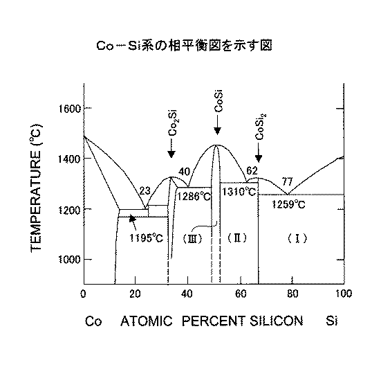
の反応が生じる。このうち、CoSi2のみが低い比抵抗(15−25μΩcm)を有している。
Reaction occurs. Of these, only CoSi 2 has a low specific resistance (15-25 μΩcm).
そこで図6において前記Co−Si系がSiリッチな組成(I)を有する場合、上記化学式1の反応に従って、一時的に反応の過程でCo2SiあるいはCoSi相が形成されても、これらは準安定相であり、最終的にはCoSi2とSiが共存した組成が得られる。これに対し、よりCoに富んだ組成(II)では、CoSiとCoSi2が共存し、さらにCoに富んだ組成(III)では高抵抗のCoSiが主な相となる。
Therefore, in FIG. 6, when the Co—Si system has a Si-rich composition (I), even if a Co 2 Si or CoSi phase is temporarily formed in the course of the reaction according to the reaction of the above
そこで、図7(A),(B)に示すようにポリシリコンゲート電極13のゲート長が充分に大きい場合には、前記ポリシリコンゲート電極13上に堆積されたCo膜14が全て反応してもCoSi2を形成するのに充分な量のSiがゲート電極13中に存在し、その結果、図7(A)の構造を600〜700℃の温度で熱処理すれば、前記ポリシリコンゲート電極13上には図7(B)に示すようにCoSi2よりなる低抵抗シリサイド層13aが形成される。ただし図7(A),(B)は、それぞれ図2(C)および図3(F)の状態に対応している。
Therefore, as shown in FIGS. 7A and 7B, when the gate length of the
これに対し、図8(A),(B)に示すように前記ポリシリコンゲート電極13のゲート長が50nm未満になると、前記Co膜14のうち、前記ポリシリコンゲート電極13上に堆積した部分のみならず、前記側壁絶縁膜13A,13B上に堆積したCo膜部分のシリサイド形成反応に対する寄与も、図8(A)中に矢印で示したCoの拡散効果により無視できなくなり、その結果、600〜700℃の熱処理を行った時点で、図8(B)に示すように前記ポリシリコンゲート電極13上には厚いシリサイド層が形成される。このようにして形成されたシリサイド層のうちでも、前記ポリシリコンゲート電極13を構成するポリシリコンに接している部分には低抵抗のCoSi2が形成されていても、前記ポリシリコンから離間したシリサイド層の上部では、シリコン原子の絶対量がゲート長の減少に伴い減少するのに加え、前記Co膜14のうち、側壁絶縁膜13A,13Bを覆う部分からのCo原子の拡散の寄与もあってSiが枯渇し、一方Coが過剰になり、高抵抗のCoSi層13a´が形成されてしまうも状況が生じうると考えられる。
On the other hand, as shown in FIGS. 8A and 8B, when the gate length of the
すなわち、先に図2で説明したシリサイドシート抵抗のばらつきは、このような高抵抗CoSi層13a´が不規則に形成されることによっても引き起こされる可能性がある。
That is, the variation in the silicide sheet resistance described above with reference to FIG. 2 may be caused by the irregular formation of such a high
本発明は一の観点において、ゲート長が50nm未満の半導体装置の製造方法であって、半導体基板上に幅が50nm未満のポリシリコンゲート電極パターンを形成する工程と、前記半導体基板中、前記ポリシリコンゲート電極パターンの両側に一対の拡散領域を形成する工程と、前記半導体基板上に、前記一対の拡散領域を覆うように、また前記ポリシリコンゲート電極パターンを覆うように、Co膜を堆積する工程と、前記Co膜上に、窒化チタン膜を堆積する工程と、前記窒化チタン膜を堆積する工程の後、前記Co膜を、前記ポリシリコンゲート電極の表面および前記一対の拡散領域の表面と反応させ、CoSi2層を形成する工程とよりなり、前記窒化チタン膜は粒径がその膜厚よりも小さくなるように形成されることを特徴とする半導体装置の製造方法を提供する。 In one aspect, the present invention provides a method for manufacturing a semiconductor device having a gate length of less than 50 nm, the step of forming a polysilicon gate electrode pattern having a width of less than 50 nm on a semiconductor substrate, Forming a pair of diffusion regions on both sides of the silicon gate electrode pattern; and depositing a Co film on the semiconductor substrate so as to cover the pair of diffusion regions and to cover the polysilicon gate electrode pattern. After the step, depositing a titanium nitride film on the Co film, and depositing the titanium nitride film, the Co film is formed on the surface of the polysilicon gate electrode and the surface of the pair of diffusion regions. reacted, becomes more a process of forming a CoSi 2 layer, the titanium nitride film to being formed so as the particle size is smaller than the thickness thereof To provide a method of manufacturing a semiconductor device.
本発明は別の観点において、ゲート長が50nm未満の半導体装置の製造方法であって、半導体基板上に幅が50nm未満のポリシリコンゲート電極パターンを形成する工程と、前記半導体基板中、前記ポリシリコンゲート電極パターンの両側に一対の拡散領域を形成する工程と、前記半導体基板上に、前記一対の拡散領域を覆うように、また前記ポリシリコンゲート電極パターンを覆うように、Co膜を堆積する工程と、前記Co膜上に、窒化チタン膜を堆積する工程と、前記窒化チタン膜を堆積する工程の後、前記Co膜を、前記ポリシリコンゲート電極の表面および前記一対の拡散領域の表面と反応させ、CoSi2層を形成する工程とよりなり、前記窒化チタン膜はアモルファス相として形成されることを特徴とする半導体装置の製造方法を提供する。 In another aspect, the present invention provides a method for manufacturing a semiconductor device having a gate length of less than 50 nm, the step of forming a polysilicon gate electrode pattern having a width of less than 50 nm on a semiconductor substrate, Forming a pair of diffusion regions on both sides of the silicon gate electrode pattern; and depositing a Co film on the semiconductor substrate so as to cover the pair of diffusion regions and to cover the polysilicon gate electrode pattern. After the step, depositing a titanium nitride film on the Co film, and depositing the titanium nitride film, the Co film is formed on the surface of the polysilicon gate electrode and the surface of the pair of diffusion regions. reacted, it becomes more and forming a CoSi 2 layer, manufacturing of a semiconductor device, characterized in that said titanium nitride film is formed as an amorphous phase To provide a method.
本発明はさらに別の観点において、ゲート長が50nm未満の半導体装置の製造方法であって、半導体基板上に幅が50nm未満のポリシリコンゲート電極パターンを形成する工程と、前記半導体基板中、前記ポリシリコンゲート電極パターンの両側に一対の拡散領域を形成する工程と、前記半導体基板上に、前記一対の拡散領域を覆うように、また前記ポリシリコンゲート電極パターンを覆うように、Co膜を堆積する工程と、前記Co膜上に、組成がTixNy(x+y=1)で表される窒化チタン膜を堆積する工程と、前記窒化チタン膜を堆積する工程の後、前記Co膜を、前記ポリシリコンゲート電極の表面および前記一対の拡散領域の表面と反応させ、CoSi2層形成する工程とよりなり、前記窒化チタン膜はx>yの組成を有することを特徴とする半導体装置の製造方法を提供する。 In still another aspect, the present invention provides a method for manufacturing a semiconductor device having a gate length of less than 50 nm, the step of forming a polysilicon gate electrode pattern having a width of less than 50 nm on a semiconductor substrate, Forming a pair of diffusion regions on both sides of the polysilicon gate electrode pattern; and depositing a Co film on the semiconductor substrate so as to cover the pair of diffusion regions and to cover the polysilicon gate electrode pattern And after depositing a titanium nitride film having a composition represented by TixNy (x + y = 1) on the Co film and depositing the titanium nitride film, the Co film is formed on the polysilicon film. It comprises a step of reacting with the surface of the gate electrode and the surface of the pair of diffusion regions to form a CoSi 2 layer, the titanium nitride film having a composition of x> y A method for manufacturing a semiconductor device is provided.
本発明によれば、ゲート長が50nm未満の半導体装置の製造方法において、半導体基板上に幅が50nm未満のポリシリコンゲート電極パターンを形成し、前記半導体基板中、前記ポリシリコンゲート電極パターンの両側に一対の拡散領域を形成し、前記半導体基板上に、前記一対の拡散領域を覆うように、また前記ポリシリコンゲート電極パターンを覆うように、Co膜を堆積し、前記Co膜上に、TiN膜を堆積し、前記TiN膜を堆積する工程の後、前記Co膜を、前記ポリシリコンゲート電極の表面および前記一対の拡散領域の表面と反応させ、CoSi2層を形成する際に、前記TiN膜を、粒径がその膜厚よりも小さくなるように形成することにより、前記TiN膜中における柱状構造の形成が抑制され、前記TiN膜を介した酸素の拡散が抑制される。その結果、Co膜中への酸素の侵入が抑制され、酸化物に起因するシリサイド形成の不均一が抑制される。 According to the present invention, in a method of manufacturing a semiconductor device having a gate length of less than 50 nm, a polysilicon gate electrode pattern having a width of less than 50 nm is formed on a semiconductor substrate, and both sides of the polysilicon gate electrode pattern in the semiconductor substrate are formed. A pair of diffusion regions is formed on the semiconductor substrate, a Co film is deposited on the semiconductor substrate so as to cover the pair of diffusion regions and the polysilicon gate electrode pattern, and TiN is deposited on the Co film. After the step of depositing a film and depositing the TiN film, the Co film is reacted with the surface of the polysilicon gate electrode and the surface of the pair of diffusion regions to form the CoSi 2 layer. By forming the film so that the particle size is smaller than the film thickness, the formation of the columnar structure in the TiN film is suppressed, and the film is passed through the TiN film. Diffusion of oxygen is suppressed. As a result, the intrusion of oxygen into the Co film is suppressed, and nonuniform silicide formation due to the oxide is suppressed.
またその際に、このように非常に薄いTiN膜は一般にアモルファス相あるいはナノグレイン構造をとるが、このようなアモルファス相あるいはナノグレイン構造のTiN膜は結晶化したTiN膜よりも多少不安定で、膜中のTi原子がその下のCo膜中に拡散により侵入する可能性が考えられる。さらにこのように非常に薄いTiN保護膜を使う場合、前記TiN膜を介した酸素の拡散は皆無ではなく、前記Co膜中に微量の酸素が導入される可能性も考えられる。これら微量のTiや酸素は、シリサイド形成には影響は与えないものの、前記Co膜中においてCo原子の移動をピニングする効果を奏することが想定される。このメカニズムによれば、ゲート電極側壁絶縁膜を覆うCo膜からポリシリコンゲート電極へのCo原子の供給路が遮断され、ポリシリコンゲート電極上面における高抵抗CoSiの形成が抑制される効果が得られると考えられる。 At that time, such a very thin TiN film generally has an amorphous phase or nanograin structure, but such an amorphous phase or nanograin structure TiN film is somewhat unstable than a crystallized TiN film, There is a possibility that Ti atoms in the film may penetrate into the Co film therebelow by diffusion. Further, when such a very thin TiN protective film is used, there is no possibility of oxygen diffusion through the TiN film, and a small amount of oxygen may be introduced into the Co film. Although these trace amounts of Ti and oxygen do not affect the formation of silicide, it is assumed that there is an effect of pinning the movement of Co atoms in the Co film. According to this mechanism, the Co atom supply path from the Co film covering the gate electrode sidewall insulating film to the polysilicon gate electrode is blocked, and the formation of high-resistance CoSi on the upper surface of the polysilicon gate electrode is suppressed. it is conceivable that.
また本発明によれば、ゲート長が50nm未満の半導体装置の製造方法において、半導体基板上に幅が50nm未満のポリシリコンゲート電極パターンを形成し、前記半導体基板中、前記ポリシリコンゲート電極パターンの両側に一対の拡散領域を形成し、前記半導体基板上に、前記一対の拡散領域を覆うように、また前記ポリシリコンゲート電極パターンを覆うように、Co膜を堆積し、前記Co膜上に、TiN膜を堆積し、前記TiN膜を堆積する工程の後、前記Co膜を、前記ポリシリコンゲート電極の表面および前記一対の拡散領域の表面と反応させ、CoSi2層を形成する際に、前記TiN膜をアモルファス相として形成することにより、前記TiN膜中における柱状構造の形成が抑制され、前記TiN膜を介した酸素の拡散が抑制される。その結果、Co膜中への酸素の侵入が抑制され、酸化物に起因するシリサイド形成の不均一が抑制される。 According to the invention, in the method of manufacturing a semiconductor device having a gate length of less than 50 nm, a polysilicon gate electrode pattern having a width of less than 50 nm is formed on the semiconductor substrate, and the polysilicon gate electrode pattern is formed in the semiconductor substrate. A pair of diffusion regions are formed on both sides, a Co film is deposited on the semiconductor substrate so as to cover the pair of diffusion regions and the polysilicon gate electrode pattern, and on the Co film, After depositing a TiN film and depositing the TiN film, the Co film is reacted with the surface of the polysilicon gate electrode and the surface of the pair of diffusion regions to form a CoSi 2 layer. By forming the TiN film as an amorphous phase, the formation of columnar structures in the TiN film is suppressed, and oxygen diffusion through the TiN film is suppressed. Is control. As a result, the intrusion of oxygen into the Co film is suppressed, and nonuniform silicide formation due to the oxide is suppressed.
また本発明によれば、ゲート長が50nm未満の半導体装置の製造方法において、半導体基板上に幅が50nm未満のポリシリコンゲート電極パターンを形成し、前記半導体基板中、前記ポリシリコンゲート電極パターンの両側に一対の拡散領域を形成し、前記半導体基板上に、前記一対の拡散領域を覆うように、また前記ポリシリコンゲート電極パターンを覆うように、Co膜を堆積し、前記Co膜上に、組成がTixNy(x+y=1)で表されるTiN膜を堆積し、前記TiN膜を堆積する工程の後、前記Co膜を、前記ポリシリコンゲート電極の表面および前記一対の拡散領域の表面と反応させ、CoSi2層を形成する際に、前記TiN膜を、x>yの組成を有するように形成することにより、前記TiN膜からCo膜中に微量のTi原子が拡散し、このようにしてCo膜中に侵入したTi原子がシリコン表面の自然酸化膜を還元する。これにより、シリサイド形成反応が、シリコン表面で均一に生じ、シート抵抗のばらつきが抑制される。また、このように前記TiN膜の組成をTiリッチとすることで、前記TiN膜中にはナノグレイン構造が生じ、柱状構造の形成が抑制される。 According to the invention, in the method of manufacturing a semiconductor device having a gate length of less than 50 nm, a polysilicon gate electrode pattern having a width of less than 50 nm is formed on the semiconductor substrate, and the polysilicon gate electrode pattern is formed in the semiconductor substrate. A pair of diffusion regions are formed on both sides, a Co film is deposited on the semiconductor substrate so as to cover the pair of diffusion regions and the polysilicon gate electrode pattern, and on the Co film, After depositing a TiN film whose composition is represented by TixNy (x + y = 1) and depositing the TiN film, the Co film reacts with the surface of the polysilicon gate electrode and the surface of the pair of diffusion regions. When the CoSi 2 layer is formed, the TiN film is formed so as to have a composition of x> y, whereby a small amount of Ti is formed from the TiN film into the Co film. The atoms diffuse, and thus Ti atoms that have penetrated into the Co film reduce the natural oxide film on the silicon surface. Thereby, the silicide formation reaction occurs uniformly on the silicon surface, and variation in sheet resistance is suppressed. Further, by making the composition of the TiN film Ti-rich in this way, a nanograin structure is generated in the TiN film, and the formation of a columnar structure is suppressed.
また本発明によれば、基板と、前記基板上にゲート絶縁膜を介して形成された、ゲート長が50nm以下のポリシリコンゲート電極と、前記基板中、前記ポリシリコンゲート電極の両側において、前記ポリシリコンゲート電極の側壁絶縁膜の外側に形成された一対の拡散領域とよりなる半導体装置において、前記ポリシリコンゲート電極の上面および前記一対の拡散領域の表面にCoSi2層を、前記CoSi2層がTiを、0.1〜1.0原子パーセントの濃度で含むように形成することにより、サリサイド工程で前記CoSi2層を形成する際の還元反応を、CoSi2層の比抵抗の増大あるいは素子分離構造エッジでのCoSi2の異常成長を招くことなく促進でき、均一な低抵抗CoSi2の形成が可能になる。 According to the invention, the substrate, the polysilicon gate electrode formed on the substrate via the gate insulating film and having a gate length of 50 nm or less, the both sides of the polysilicon gate electrode in the substrate, in a more becomes a semiconductor device and a pair of diffusion regions formed on the outside of the sidewall insulation films of the polysilicon gate electrode, a CoSi 2 layer on the upper surface and the surface of the pair of diffusion regions of the polysilicon gate electrode, the CoSi 2 layer Forming Ti at a concentration of 0.1 to 1.0 atomic percent, the reduction reaction when forming the CoSi 2 layer in the salicide process can increase the specific resistance of the CoSi 2 layer or the device. It can be promoted without causing abnormal growth of CoSi 2 at the edge of the separation structure, and uniform low-resistance CoSi 2 can be formed.
[原理]
図9は、本発明の原理を示す。
[principle]
FIG. 9 illustrates the principle of the present invention.
図9を参照するに、本発明ではポリシリコンゲート電極などのシリコン面1に、Co膜2との反応によりシリサイド層を形成する際に、保護膜として前記Co膜2上に堆積されるTiN膜3を、図5の場合のような柱状構造を有する膜ではなく、アモルファス膜あるいはナノグレイン構造を有する膜として形成する。ナノグレイン構造では、TiN膜中に含まれるTiN結晶の粒径は、例えば10nm程度あるいはそれ以下で、前記TiN膜の膜厚よりも小さい。
Referring to FIG. 9, in the present invention, when a silicide layer is formed on a
この場合、図5の場合のような膜の一方の側から他方の側に連続する粒界は実質的に存在せず、前記TiN膜3を介したCo膜への酸素の侵入が効果的に抑制され、前記シリコン面1における自然酸化膜形成、およびこれに伴うシリサイド膜のシート抵抗ばらつきが効果的に抑制される。
In this case, there is substantially no grain boundary continuous from one side to the other side of the film as in the case of FIG. 5, and oxygen intrusion into the Co film through the
このようなアモルファス相あるいはナノグレイン構造を有するTiN膜3は、成膜時の膜厚を減少させることにより実現することが可能である。
The
図10は、本発明の発明者が本発明の基礎となる研究において見出した、スパッタ成膜されたTiN膜の膜厚とX線回折図形との関係を示す。 FIG. 10 shows the relationship between the film thickness of the sputter-deposited TiN film and the X-ray diffraction pattern, which the inventors of the present invention have found in the research that forms the basis of the present invention.
図10を参照するに、TiN膜はスパッタパワーを9kWに設定し,スパッタ雰囲気中のN2/Ar比を90/50(SCCM比)として行っているが、膜厚が20nm以下の場合、TiN(111)の回折ピークは全く観察されないのがわかる。これに対し、膜厚が30nmを超えると前記TiN(111)のピークが現れはじめ、膜中において結晶化が進行しているのがわかる。TiN(200)の回折ピークについても同じである。 Referring to FIG. 10, for the TiN film, the sputtering power is set to 9 kW and the N 2 / Ar ratio in the sputtering atmosphere is 90/50 (SCCM ratio). It can be seen that the diffraction peak of (111) is not observed at all. On the other hand, when the film thickness exceeds 30 nm, the TiN (111) peak begins to appear, and it can be seen that crystallization proceeds in the film. The same applies to the diffraction peak of TiN (200).
図11は、図9のモデル構造において様々な膜厚のTiN保護膜13を形成し、形成されたCoSi2層のシート抵抗のはらつきを調べた結果を示す。
FIG. 11 shows the result of examining the variation in sheet resistance of the formed CoSi 2 layer by forming the TiN
図11を参照するに、シリサイド形成工程におけるTiN保護膜13の膜厚が10nmあるいは20nmの場合にはシート抵抗にはらつきはほとんど見られないのに対し、TiN保護膜13の膜厚が30nm以上になると、ばらつきが急激に増大しているのがわかる。
Referring to FIG. 11, when the thickness of the TiN
図11の結果は、このように前記TiN保護膜13を30nm未満の膜厚、好ましくは20nm以下の膜厚に形成しておくことにより、前記TiN保護膜13中にナノグレイン構造が形成され、シリサイド形成時の熱処理の際、雰囲気中の残留酸素が前記TiN膜13を通ってCo膜12に侵入するのが効果的に抑制されていることを示している。
The result of FIG. 11 is that a nanograin structure is formed in the TiN
一方、このようにTiN膜13の膜厚を20nm以下、例えば数ナノメートル程度まで減少させた場合、先にも述べたようにTiN膜13はナノグレイン構造あるいはアモルファス状態をとり、その結果、膜中のTi原子がその下のCo膜中に拡散する可能性が考えられる。また、このように非常に薄いTiN膜13では、雰囲気中の残留酸素のCo膜12への拡散は完全には遮断されず、微量の酸素が前記Co膜12中に侵入する可能性がある。
On the other hand, when the thickness of the
このようにCo膜12中にTiや酸素が侵入した場合、これらの不純物はシリサイド形成に影響を及ぼさない程度に微量であっても、前記Co膜12中のCo原子の移動をピニングする効果を奏し、その結果、これらの不純物元素は、先の図8(A)に対応する図12に示すように、前記Co膜14が前記ポリシリコンゲート電極13の側壁絶縁膜13A,13Bを覆う部分において、シリサイド形成がなされるポリシリコンゲート電極13上部へのCo原子の供給を抑制する効果を生じる可能性が考えられる。その結果、超微細化半導体装置において、前記ゲート電極13のゲート長が縮小され、低抵抗CoSi2形成のためのSi原子の総量が不足する恐れがあるような場合、本発明の構成によればCo原子の供給を抑制することができ、シリサイド形成反応の結果、ポリシリコンゲート電極13の上部に高抵抗CoSiが形成されてしまいCoSi2層のシート抵抗がばらつく問題を回避することができるものと考えられる。
Thus, when Ti or oxygen penetrates into the
さらに本発明は、図9のモデル構造において前記TiN膜3を、Tiに富んだ非化学量論組成TixNy(x+y=1)を有するように形成することで、シリサイド形成反応の不均一性を抑制する技術を提供する。
Furthermore, the present invention suppresses non-uniformity of the silicide formation reaction by forming the
図13は、通常のスパッタ条件により形成したTiN膜と、本発明による非化学量論組成を有するTiN膜のX線回折図形を、金属Ti膜のものと比較して示す図である。 FIG. 13 is a diagram showing an X-ray diffraction pattern of a TiN film formed under normal sputtering conditions and a TiN film having a non-stoichiometric composition according to the present invention compared with that of a metal Ti film.
図13を参照するに、図示の通常条件の例ではTiN膜を、9keVのスパッタパワーを使い、窒素ガスを100SCCM,Arガスを50SCCMの流量で供給し、30nmの膜厚に形成しているが、この場合には、明瞭なTiN(111)の回折ピークおよび不明瞭なTiN(200)の回折ピークが現れているのが確認される。 Referring to FIG. 13, in the example of the normal conditions shown in the figure, the TiN film is formed to a thickness of 30 nm by using a sputtering power of 9 keV, supplying nitrogen gas at a flow rate of 100 SCCM, and Ar gas at a flow rate of 50 SCCM. In this case, it is confirmed that a clear TiN (111) diffraction peak and an unclear TiN (200) diffraction peak appear.
これに対し、図13の本発明では前記TiN膜3のスパッタを、3keVの加速電圧下、窒素ガスおよびArガスをそれぞれ20SCCMおよび100SCCMの流量で供給することで行っているが、この場合にはTiN(111)あるいは(200)の回折ピークは全く生じていないことがわかる。すなわち、このようにして形成されたTiN膜はアモルファス構造を有していると考えられる。
In contrast, in the present invention of FIG. 13, the
図9のモデル構造において、このようにTiに富んだアモルファスTiN膜を保護膜としてシリサイド形成を行った場合、TiN保護膜3からCo膜2にTi原子が供給され、このようにして供給されたTi原子は前記Co膜2とシリコン面1との界面において自然酸化膜を還元すると考えられる。また、先に説明したように、このようにCo膜2中に侵入したTi原子はCo膜2中におけるCo原子の移動をピニングし、シリサイド形成が生じるポリシリコンゲート電極13の上部へのCo原子の供給を抑制する効果も奏する可能性も考えられる。
In the model structure of FIG. 9, when silicide formation is performed using the Ti-rich amorphous TiN film as a protective film, Ti atoms are supplied from the TiN
図14は、図9のモデル構造において上記本発明の条件で50nmの厚さに形成されたTiN膜13を保護膜として形成されたCoSi2層におけるシート抵抗のばらつきを、上記通常条件で形成されたCoSi2層のシート抵抗ばらつきと比較して示す図である。
FIG. 14 shows the variation in sheet resistance in the CoSi 2 layer formed using the
図14を参照するに、本発明の条件で形成したTiに富むアモルファスTiN膜3を保護膜3としてシリサイド形成を行った場合、TiN膜3の膜厚が50nmであっても、シリサイド層のシート抵抗ばらつきがほとんど生じないことがわかる。一方、通常条件でTiN保護膜3を形成した場合には、前記TiN保護膜3の膜厚が30nmであっても、非常に大きなシート抵抗のばらつきが生じているのがわかる。
Referring to FIG. 14, when silicide formation is performed using the Ti-rich
ところで前記Co膜中にTiが1原子パーセント以上の濃度で含まれるような場合には、形成されるCoSi2層の比抵抗が増加してしまい、またSTI領域11Bのエッジ部におけるCoSi2の異常成長によるリーク電流の増大の問題が生じる。また前記Co膜中のTi濃度が低すぎると、先に述べたTiによるシリコン表面の自然酸化膜の還元反応が抑制され、シート抵抗のばらつきを抑制できない。このようなことから、前記TiN膜の組成は、CoSi2層中のTi濃度が0.1〜1.0原子%となるように設定するのが好ましい。
By the way, when Ti is contained in the Co film at a concentration of 1 atomic percent or more, the specific resistance of the formed CoSi 2 layer increases, and an abnormality of CoSi 2 at the edge of the
またこれに対応して、本発明では前記TiN膜をTiに富んだ非化学量論組成を有するように形成する場合、前記TiN膜の組成TixNy(x+y=1)を、1.0<x/y<5.0の範囲に選ぶのが好ましい。 Correspondingly, in the present invention, when the TiN film is formed to have a non-stoichiometric composition rich in Ti, the composition TixNy (x + y = 1) of the TiN film is set to 1.0 <x / It is preferable to select the range of y <5.0.
TiN膜中におけるTi/N組成比は、前記TiN膜をスパッタで形成する場合、スパッタ雰囲気中の窒素/Ar濃度比を調節することにより、変化させることができる(非特許文献2参照)。また、TiN膜をアモルファス相で形成する、あるいはTiN膜を、ナノグレイン構造を有するように形成するには、スパッタ成膜時に基板バイアスを印加する方法が可能である(非特許文献3,4参照)。あるいは、TiN膜の膜厚を減少させることによっても可能である(非特許文献5参照)。
The Ti / N composition ratio in the TiN film can be changed by adjusting the nitrogen / Ar concentration ratio in the sputtering atmosphere when the TiN film is formed by sputtering (see Non-Patent Document 2). Further, in order to form the TiN film in an amorphous phase, or to form the TiN film so as to have a nanograin structure, a method of applying a substrate bias at the time of sputtering film formation is possible (see
以下、上記の原理に基づく、本発明の半導体装置の製造方法を、実施例について説明する。
[第1実施例]
図15(A)〜16(F)は、本発明の第1実施例によるMOSトランジスタの製造工程を示す。
Embodiments of the semiconductor device manufacturing method of the present invention based on the above principle will be described below.
[First embodiment]
15 (A) to 16 (F) show a manufacturing process of the MOS transistor according to the first embodiment of the present invention.
図15(A)を参照するに、典型的にはp型のシリコン基板21上にSTI型の素子分離構造21Bにより、素子領域21Aが画成されており、前記素子領域21Aにはp型あるいはn型のウェル21Wが形成されている。さらに前記素子領域21Aにおいては前記シリコン基板21上に厚さが例えば2nmのシリコン酸化膜あるいは酸窒化膜よりなるゲート絶縁膜22を介して高さが例えば100nmのポリシリコンゲート電極23が、50nmあるいはそれ以下のゲート長に形成されている。
Referring to FIG. 15A, typically, an
前記ポリシリコンゲート電極23は、前記MOSトランジスタがnチャネルMOSトランジスタの場合には、例えばP+を10keVの加速電圧下、1×1016cm-2のドーズ量でイオン注入することにより、n型にドープされている。一方、前記MOSトランジスタがpチャネルMOSトランジスタの場合には、前記ポリシリコンゲート電極23は、例えばB+を5keVの加速電圧下、5×1015cm-2のドーズ量でイオン注入することにより、p型にドープされている。
In the case where the MOS transistor is an n-channel MOS transistor, the
また前記素子領域21Aではシリコン基板21の表面が、前記MOSトランジスタがnチャネルMOSトランジスタの場合、例えばB+を15keVの加速電圧下、1×1013cm-2のドーズ量でイオン注入することにより、p型にチャネルドープされている。また前記MOSトランジスタがpチャネルMOSトランジスタの場合には、前記シリコン基板21の表面が、例えばAs+を80keVの加速電圧下、1×1013cm-2のドーズ量でイオン注入することにより、n型にチャネルドープされている。
In the
また前記素子領域21Aでは前記シリコン基板中、前記ポリシリコンゲート電極23の両側にn型あるいはp型の拡散領域21a,21bが、それぞれソースエクステンション領域およびドレインエクステンション領域として形成されている。前記MOSトランジスタがnチャネルMOSトランジスタの場合には、前記ソースエクステンション領域21aおよびドレインエクステンション領域21bは、例えばAs+を1keVの加速電圧下、1×1015cm-2のドーズ量でイオン注入することにより形成することができる。また前記MOSトランジスタがpチャネルMOSトランジスタの場合には、前記ソースエクステンション領域21aおよびドレインエクステンション領域21bは、例えばB+を0.5keVの加速電圧下、5×1015cm-2のドーズ量でイオン注入することにより形成することができる。
In the
前記ソースおよびドレインエクステンション領域21a,21bの形成の後、前記シリコン基板21上には前記ゲート電極23を覆うように、厚さが例えば100nmの酸化膜がCVD法により堆積され、これをRIE法によりエッチバックすることにより、前記ゲート電極23の両側壁面には、側壁絶縁膜23A,23Bが形成されている。
After the formation of the source and
さらに図15(A)の構造では、前記ゲート電極23および側壁絶縁膜23A,23Bをマスクに、n型あるいはp型不純物元素をイオン注入することにより、前記ソースエクステンション領域21aに部分的に重畳して、同一導電型のソース領域21cが、また前記ドレインエクステンション領域21bに部分的に重畳して、同一導電型のドレイン領域21dが形成されている。前記MOSトランジスタがnチャネルMOSトランジスタである場合、前記ソース領域21cおよびドレイン領域21dは、例えばP+を10keVの加速電圧下、1×1016cm-2のドーズ量でイオン注入することにより形成できる。さらに前記MOSトランジスタがpチャネルMOSトランジスタである場合には、前記ソース領域10cおよびドレイン領域10dは、例えばB+を5keVの加速電圧下、5×1015cm-2のドーズ量でイオン注入することにより、形成することができる。
Further, in the structure of FIG. 15A, an n-type or p-type impurity element is ion-implanted using the
次に図15(B)の工程において、図15(A)の構造をフッ酸処理し、前記ゲート電極22およびソース/ドレイン領域23c、23d表面の自然酸化膜を除去する。さらに、Coターゲットを用いて、このようにフッ酸処理した図15(A)の構造上にCo膜24を、例えば6nmの厚さに、スパッタリングにより堆積する。ただし、前記Co膜24の成膜方法はスパッタリングに限定されるものではなく、他の堆積方法、例えば電子ビーム蒸着法を使うことも可能である。ここで、最終的に形成されるシリサイド層の比抵抗を考慮すると、前記Co膜24の膜厚は、4〜7nmの範囲に設定するのが好ましい。
Next, in the step of FIG. 15B, the structure of FIG. 15A is treated with hydrofluoric acid to remove the natural oxide film on the surface of the
次に、図15(C)の工程において、図15(B)の構造上に保護膜として。TiN膜25を、スパッタリングにより、スパッタパワーを例えば9kW、スパッタ雰囲気中のN2/Ar比を例えば100/50(sccm比)、基板バイアスを例えば−100Vに設定することにより、30nmの膜厚に堆積する。ここで、前記基板バイアスは、TiN堆積速度が、バイアスを印加しない場合と比較して90%以上、99%以下になるように調節する。基板バイアスが小さい場合、得られるTiN膜25は、ナノグレイン構造を有し、一方前記基板バイアスが上記のように大きい場合には、前記TiN膜25はアモルファス化される。すなわち本実施例では、前記TiN膜25堆積時の基板バイアスを上記のように大きな値に設定することで、前記TiN膜25を、先に図10で説明したようにアモルファス相として形成する。
Next, in the step of FIG. 15C, as a protective film over the structure of FIG. The
次に図16(D)の工程において、図15(C)の構造には例えば480℃で30秒間、急速熱処理(RTA処理)が施され、その結果、前記Co膜24とソース領域21cあるいはドレイン領域21dの界面、および前記Co膜24とポリシリコンゲート電極23との界面には、CoSi層121e,121fおよび123aが、それぞれ形成される。なお、図16(D)のシリサイド形成工程は、前記RTA処理の代わりに炉アニールにより行うことも可能である。またこのシリサイド形成工程を、炉アニールとRTA処理を併用して行うことも可能である。
Next, in the step of FIG. 16D, the structure of FIG. 15C is subjected to a rapid thermal treatment (RTA treatment) at, for example, 480 ° C. for 30 seconds. As a result, the
次に図16(E)の工程において、図15(C)の構造をウェットエッチング処理し(硫酸:過酸化水素水=3:1、20分)、前記保護膜25および素子分離構造21Bあるいは側壁絶縁膜23A,23Bなど、絶縁膜上の未反応Co膜24を選択的にエッチング除去する。
Next, in the step of FIG. 16E, the structure of FIG. 15C is wet-etched (sulfuric acid: hydrogen peroxide solution = 3: 1, 20 minutes), and the
さらに図16(F)の工程で、第2の急速熱処理を750℃で30秒間行い、先に形成されたCoSi層121e,121fおよび123aをCoSi2層21e,21fおよび23aに変換する。なお、この図16(F)の急速熱処理は、熱処理を650〜800℃程度の温度で10〜120秒程度行うことにより行ってもよい。あるいは、800〜1000℃のスパイクアニールにより行うことも可能である。
Further, in the step of FIG. 16F, the second rapid thermal treatment is performed at 750 ° C. for 30 seconds to convert the previously formed
図16(F)の工程の後、SiNエッチングストッパ膜を図16(F)の構造上に形成し、さらに層間絶縁膜を形成した後、前記ソース領域21c,ドレイン領域21dおよびゲート電極23において前記CoSi層21e,21fおよび23aを露出するようにコンタクトホールを形成し、さらにかかるコンタクトホールをビアプラグで充填する。
After the step of FIG. 16F, an SiN etching stopper film is formed on the structure of FIG. 16F, and further an interlayer insulating film is formed. Then, the
本実施例によれば、図15(C)の工程において前記TiN保護膜25をアモルファス相あるいはナノグレイン構造を有するように形成しているため、図9のモデル構造で説明したように、熱処理工程の際の雰囲気中に残留している酸素が前記Co膜24に侵入し、シリサイドが形成されるシリコン面に新たな酸化膜を形成してしまう問題が生じることがなく、CoSi2の形成が、前記ソース領域21c,ドレイン領域21dおよびポリシリコンゲート電極23aの表面において一様に生じる。その結果、前記CoSi2層21e,21fおよび23aにおいて、先に図11あるいは14で説明したのと同様な、ばらつきの少ない、一様なシート抵抗が、実現される。
[第2実施例]
本発明の第2実施例でも、先に説明した図15(A)〜16(F)と同様の工程により半導体装置の製造を行うが、本実施例では図15(C)の工程において前記TiN保護膜25の堆積を、スパッタパワーを3kWに設定し、窒素ガスおよびArガスをそれぞれ20SCCMおよび100SCCMの流量で供給することにより(N2/Ar比=20/100)、前記TiN保護膜が例えば30nmの膜厚を有するように実行する。ここで、前記スパッタ条件は、Ti/N組成比が1〜5となるようにパワーおよびN2/Ar比を調節され、その結果、得られるTiN保護膜25は、Tiに富んだアモルファス膜となる。
According to the present embodiment, since the TiN
[Second Embodiment]
Also in the second embodiment of the present invention, a semiconductor device is manufactured by the same process as that of FIGS. 15A to 16F described above. In this embodiment, the TiN is manufactured in the process of FIG. The
本実施例ではこのように図15(C)の工程においてTiN保護膜25を形成した後、先の実施例と同様に図16(D)の工程において第1の急速熱処理を、例えば480℃で30秒行い、前記ソース領域21c,ドレイン領域21dおよびポリシリコンゲート電極23の表面にCoSi層121e,121f,123aをそれぞれ形成する。
In this embodiment, after the TiN
先の実施例と同様に、前記急速熱処理の代わりに炉アニール処理を行うことも可能で、また炉アニールに急速熱処理を組み合わせた処理を行うことも可能である。 As in the previous embodiment, a furnace annealing process can be performed instead of the rapid thermal process, and a process combining the furnace annealing with the rapid thermal process can also be performed.
次に図16(E)の工程において、前記TiN保護膜25および未反応Co膜24がウェットエッチング処理により除去され、さらに図16(E)の工程において第2の急速熱処理工程を例えば750℃で30秒間行うことにより、前記CoSi層121e,121fおよび123aをCoSi2層21e,21fおよび23aに変換する。先の実施例と同様に、前記第2の急速熱処理工程は、650〜800℃程度の温度で10秒〜120秒程度の時間行うことができる。また前記第2の熱処理工程は、800〜1000℃のスパイクアニールにより行うことも可能である。
Next, in the step of FIG. 16 (E), the TiN
本実施例によれば、図15(C)の工程において前記TiN保護膜25をTiに富んだアモルファス相として形成しているため、前記TiN保護膜25からCo膜24に供給されたTi原子が、前記ソース領域21c,ドレイン領域21dあるいはポリシリコンゲート電極23a表面の酸化膜、例えば残留している自然酸化膜などを還元することにより除去し、このため、CoSi2の形成が、前記ソース領域21c,ドレイン領域21dおよびポリシリコンゲート電極23aの表面において一様に生じる。その結果、先に図11あるいは14で説明したのと同様な、ばらつきの少ない、一様なシート抵抗が、前記CoSi2層21e,21fおよび23aにおいて実現される。この効果に加えて、前記TiN保護膜25中の酸素原子の拡散路が、アモルファス構造により遮断されるため、熱処理時に雰囲気中の残留酸素により、前記シリコン表面に新たな酸化膜が形成され、シリサイド形成が不均一になる問題も解消する。
According to this embodiment, since the TiN
さらに、先にも説明したように、Co膜24中に侵入したTi原子は、Co膜24中におけるCo原子の移動をピニングし、これにより、シリサイド形成が生じるポリシリコンゲート電極13の上部へのCo原子の供給を抑制する効果をも奏する可能性がある。
[第3実施例]
本発明の第3実施例でも、先に説明した図15(A)〜16(F)と同様の工程により半導体装置の製造を行うが、本実施例では図15(C)の工程において、前記TiN保護膜25の堆積を、スパッタパワーを9kWに設定し、窒素ガスおよびArガスをそれぞれ90SCCMおよび50SCCMの流量で供給することにより(N2/Ar比=90/50)前記TiN膜25が10nmの厚さに堆積するように実行する。その際、本実施例では前記TiN膜25がナノグレイン構造を有するように形成するために、その膜厚を20nmに設定する。先に説明した図10の関係を参照。
Further, as described above, the Ti atoms that have entered the
[Third embodiment]
Also in the third embodiment of the present invention, a semiconductor device is manufactured by the same process as that shown in FIGS. 15A to 15F described above. In this embodiment, in the process of FIG. The TiN
本実施例ではこのように図15(C)の工程においてTiN保護膜25を形成した後、先の実施例と同様に図16(D)の工程において第1の急速熱処理を、例えば480℃で30秒行い、前記ソース領域21c,ドレイン領域21dおよびポリシリコンゲート電極23の表面にCoSi層121e,121f,123aをそれぞれ形成する。
In this embodiment, after the TiN
先の実施例と同様に、前記急速熱処理の代わりに炉アニール処理を行うことも可能で、また炉アニールに急速熱処理を組み合わせた処理を行うことも可能である。 As in the previous embodiment, a furnace annealing process can be performed instead of the rapid thermal process, and a process combining the furnace annealing with the rapid thermal process can also be performed.
次に図16(E)の工程において、前記TiN保護膜25および未反応Co膜24がウェットエッチング処理により除去され、さらに図16(E)の工程において第2の急速熱処理工程を例えば750℃で30秒間行うことにより、前記CoSi層121e,121fおよび123aをCoSi2層21e,21fおよび23aに変換する。先の実施例と同様に、前記第2の急速熱処理工程は、650〜800℃程度の温度で10秒〜120秒程度の時間行うことができる。また前記第2の熱処理工程は、800〜1000℃のスパイクアニールにより行うことも可能である。
Next, in the step of FIG. 16 (E), the TiN
本実施例によれば、図15(C)の工程において前記TiN保護膜25を20nm以下の膜厚に形成しているため、前記TiN保護膜25はナノグレイン構造を有し、前記TiN保護膜25中の酸素原子の拡散路が遮断される。このため、図16(D)あるいは16(F)の熱処理工程の際に、雰囲気中の残留酸素により、前記シリコン表面に新たな酸化膜が形成され、シリサイド形成が不均一になる問題が解消される。また、本実施例ではTiN保護膜25の膜厚が小さいため、熱処理雰囲気中の残留酸素のうち、わずかの部分が膜中を拡散してCo膜24に到達することが可能で、このようにしてCo膜24中に取り込まれた酸素原子は、特に前記Co膜24がゲート電極23の側壁絶縁膜23A,23Bを覆う領域において、前記TiN保護膜25より拡散したTi原子とともに、先に図12で説明したCo膜24中におけるCo原子の移動をピニングする効果を生じる可能性がある。その結果、図16(F)のCoSi2層形成のための熱処理工程において、このようなCo膜24のうち前記側壁絶縁膜23A,23Bを覆う部分からのCo原子の、シリサイド形成反応が生じるポリシリコンゲート電極23の上部への供給が抑制され、図16(F)の熱処理工程において、Co原子の過剰およびSi原子の枯渇により高抵抗CoSiが形成され、CoSi2層21c,21dあるいは23aのシート抵抗のばらつきが生じる問題が抑制される。
According to this embodiment, since the TiN
以上、本発明を好ましい実施例について説明したが、本発明はかかる特定の実施例に限定されるものではなく、特許請求の範囲に記載した要旨内において様々な変形・変更が可能である。 Although the present invention has been described with reference to the preferred embodiments, the present invention is not limited to such specific embodiments, and various modifications and changes can be made within the scope described in the claims.
1 シリコン基板
2 Co膜
3 TiN保護膜
11,21 シリコン基板
11A,21A 素子領域
11B,21B 素子分離領域
11W,21W ウェル
11a,21a ソースエクステンション領域
11b,21b ドレインエクステンション領域
11c,21c ソース領域
11d,21d ドレイン領域
11e,11f,13a,21e,21f,23a CoSi2層
12,22 ゲート絶縁膜
13,23 ゲート電極
13A,13B,23A,23B ゲート側壁絶縁膜
14,24 Co膜
15,25 TiN保護膜
111e,111f,113a,121c,121f,123a CoSi層
DESCRIPTION OF
Claims (10)
半導体基板上に幅が50nm未満のポリシリコンゲート電極パターンを形成する工程と、
前記半導体基板中、前記ポリシリコンゲート電極パターンの両側に一対の拡散領域を形成する工程と、
前記半導体基板上に、前記一対の拡散領域を覆うように、また前記ポリシリコンゲート電極パターンを覆うように、コバルト膜を堆積する工程と、
前記コバルト膜上に、窒化チタン膜を堆積する工程と、
前記窒化チタン膜を堆積する工程の後、前記コバルト膜を、前記ポリシリコンゲート電極の表面および前記一対の拡散領域の表面と反応させ、CoSi2層を形成する工程とよりなり、
前記窒化チタン膜は粒径がその膜厚よりも小さくなるように形成されることを特徴とする半導体装置の製造方法。 A method of manufacturing a semiconductor device having a gate length of less than 50 nm,
Forming a polysilicon gate electrode pattern having a width of less than 50 nm on a semiconductor substrate;
Forming a pair of diffusion regions on both sides of the polysilicon gate electrode pattern in the semiconductor substrate;
Depositing a cobalt film on the semiconductor substrate to cover the pair of diffusion regions and to cover the polysilicon gate electrode pattern;
Depositing a titanium nitride film on the cobalt film;
After the step of depositing the titanium nitride film, the cobalt film is reacted with the surface of the polysilicon gate electrode and the surface of the pair of diffusion regions to form a CoSi 2 layer,
The method of manufacturing a semiconductor device, wherein the titanium nitride film is formed to have a particle size smaller than the film thickness.
半導体基板上に幅が50nm未満のポリシリコンゲート電極パターンを形成する工程と、
前記半導体基板中、前記ポリシリコンゲート電極パターンの両側に一対の拡散領域を形成する工程と、
前記半導体基板上に、前記一対の拡散領域を覆うように、また前記ポリシリコンゲート電極パターンを覆うように、コバルト膜を堆積する工程と、
前記コバルト膜上に、窒化チタン膜を堆積する工程と、
前記窒化チタン膜を堆積する工程の後、前記コバルト膜を、前記ポリシリコンゲート電極の表面および前記一対の拡散領域の表面と反応させ、CoSi2層を形成する工程とよりなり、
前記窒化チタン膜はアモルファス相として形成されることを特徴とする半導体装置の製造方法。 A method of manufacturing a semiconductor device having a gate length of less than 50 nm,
Forming a polysilicon gate electrode pattern having a width of less than 50 nm on a semiconductor substrate;
Forming a pair of diffusion regions on both sides of the polysilicon gate electrode pattern in the semiconductor substrate;
Depositing a cobalt film on the semiconductor substrate to cover the pair of diffusion regions and to cover the polysilicon gate electrode pattern;
Depositing a titanium nitride film on the cobalt film;
After the step of depositing the titanium nitride film, the cobalt film is reacted with the surface of the polysilicon gate electrode and the surface of the pair of diffusion regions to form a CoSi 2 layer,
The method of manufacturing a semiconductor device, wherein the titanium nitride film is formed as an amorphous phase.
半導体基板上に幅が50nm未満のポリシリコンゲート電極パターンを形成する工程と、
前記半導体基板中、前記ポリシリコンゲート電極パターンの両側に一対の拡散領域を形成する工程と、
前記半導体基板上に、前記一対の拡散領域を覆うように、また前記ポリシリコンゲート電極パターンを覆うように、コバルト膜を堆積する工程と、
前記コバルト膜上に、組成がTixNy(x+y=1)で表される窒化チタン膜を堆積する工程と、
前記窒化チタン膜を堆積する工程の後、前記コバルト膜を、前記ポリシリコンゲート電極の表面および前記一対の拡散領域の表面と反応させ、CoSi2層を形成する工程とよりなり、
前記窒化チタン膜はx>yの組成を有することを特徴とする半導体装置の製造方法。 A method of manufacturing a semiconductor device having a gate length of less than 50 nm,
Forming a polysilicon gate electrode pattern having a width of less than 50 nm on a semiconductor substrate;
Forming a pair of diffusion regions on both sides of the polysilicon gate electrode pattern in the semiconductor substrate;
Depositing a cobalt film on the semiconductor substrate to cover the pair of diffusion regions and to cover the polysilicon gate electrode pattern;
Depositing a titanium nitride film having a composition represented by TixNy (x + y = 1) on the cobalt film;
After the step of depositing the titanium nitride film, the cobalt film is reacted with the surface of the polysilicon gate electrode and the surface of the pair of diffusion regions to form a CoSi 2 layer,
The method of manufacturing a semiconductor device, wherein the titanium nitride film has a composition of x> y.
前記基板上にゲート絶縁膜を介して形成された、ゲート長が50nm以下のポリシリコンゲート電極と、
前記基板中、前記ポリシリコンゲート電極の両側において、前記ポリシリコンゲート電極の側壁絶縁膜の外側に形成された一対の拡散領域とよりなる半導体装置であって、
前記ポリシリコンゲート電極の上面および前記一対の拡散領域の表面にはCoSi2層が形成されており、
前記CoSi2層はTiを、0.1〜1.0原子パーセントの濃度で含むことを特徴とする半導体装置。
A substrate,
A polysilicon gate electrode having a gate length of 50 nm or less formed on the substrate via a gate insulating film;
A semiconductor device comprising a pair of diffusion regions formed outside the sidewall insulating film of the polysilicon gate electrode on both sides of the polysilicon gate electrode in the substrate;
A CoSi 2 layer is formed on the upper surface of the polysilicon gate electrode and the surfaces of the pair of diffusion regions,
The CoSi 2 layer contains Ti at a concentration of 0.1 to 1.0 atomic percent.
Priority Applications (2)
| Application Number | Priority Date | Filing Date | Title |
|---|---|---|---|
| JP2004299280A JP2006114633A (en) | 2004-10-13 | 2004-10-13 | Manufacturing method of semiconductor device |
| US11/041,217 US20060079087A1 (en) | 2004-10-13 | 2005-01-25 | Method of producing semiconductor device |
Applications Claiming Priority (1)
| Application Number | Priority Date | Filing Date | Title |
|---|---|---|---|
| JP2004299280A JP2006114633A (en) | 2004-10-13 | 2004-10-13 | Manufacturing method of semiconductor device |
Publications (1)
| Publication Number | Publication Date |
|---|---|
| JP2006114633A true JP2006114633A (en) | 2006-04-27 |
Family
ID=36145916
Family Applications (1)
| Application Number | Title | Priority Date | Filing Date |
|---|---|---|---|
| JP2004299280A Pending JP2006114633A (en) | 2004-10-13 | 2004-10-13 | Manufacturing method of semiconductor device |
Country Status (2)
| Country | Link |
|---|---|
| US (1) | US20060079087A1 (en) |
| JP (1) | JP2006114633A (en) |
Cited By (2)
| Publication number | Priority date | Publication date | Assignee | Title |
|---|---|---|---|---|
| KR100776174B1 (en) * | 2006-08-24 | 2007-11-12 | 동부일렉트로닉스 주식회사 | Semiconductor device including silicide and manufacturing method thereof |
| JP2012528488A (en) * | 2009-05-28 | 2012-11-12 | コヴィオ インコーポレイテッド | Semiconductor device on substrate coated with diffusion barrier and method of forming the same |
Families Citing this family (4)
| Publication number | Priority date | Publication date | Assignee | Title |
|---|---|---|---|---|
| CN102122613A (en) * | 2010-01-08 | 2011-07-13 | 中芯国际集成电路制造(上海)有限公司 | Method for forming self-aligning metal silicide |
| CN103515217A (en) * | 2012-06-26 | 2014-01-15 | 中芯国际集成电路制造(上海)有限公司 | Formation method of metal silicide layer and formation method of NMOS transistor |
| US10811262B2 (en) * | 2016-01-14 | 2020-10-20 | Taiwan Semiconductor Manufacturing Co., Ltd. | Semiconductor device having a uniform and thin silicide layer on an epitaxial source/ drain structure and manufacturing method thereof |
| EP4376054A1 (en) * | 2022-11-23 | 2024-05-29 | EM Microelectronic-Marin SA | Method of manufacturing an integrated circuit to overcome defects or dislocations |
Family Cites Families (5)
| Publication number | Priority date | Publication date | Assignee | Title |
|---|---|---|---|---|
| GB2324882B (en) * | 1997-04-29 | 2001-05-23 | Daewoo Electronics Co Ltd | Array of thin film actuated mirrors and method for the manufacture thereof |
| JP3523093B2 (en) * | 1997-11-28 | 2004-04-26 | 株式会社東芝 | Semiconductor device and manufacturing method thereof |
| US20020061639A1 (en) * | 2000-10-02 | 2002-05-23 | Kazuichiroh Itonaga | Semiconductor device and method for manufacturing the same |
| JP2004140315A (en) * | 2002-10-17 | 2004-05-13 | Samsung Electronics Co Ltd | Method for manufacturing semiconductor device using salicide process |
| US6936528B2 (en) * | 2002-10-17 | 2005-08-30 | Samsung Electronics Co., Ltd. | Method of forming cobalt silicide film and method of manufacturing semiconductor device having cobalt silicide film |
-
2004
- 2004-10-13 JP JP2004299280A patent/JP2006114633A/en active Pending
-
2005
- 2005-01-25 US US11/041,217 patent/US20060079087A1/en not_active Abandoned
Cited By (2)
| Publication number | Priority date | Publication date | Assignee | Title |
|---|---|---|---|---|
| KR100776174B1 (en) * | 2006-08-24 | 2007-11-12 | 동부일렉트로닉스 주식회사 | Semiconductor device including silicide and manufacturing method thereof |
| JP2012528488A (en) * | 2009-05-28 | 2012-11-12 | コヴィオ インコーポレイテッド | Semiconductor device on substrate coated with diffusion barrier and method of forming the same |
Also Published As
| Publication number | Publication date |
|---|---|
| US20060079087A1 (en) | 2006-04-13 |
Similar Documents
| Publication | Publication Date | Title |
|---|---|---|
| US6562718B1 (en) | Process for forming fully silicided gates | |
| US7397091B2 (en) | SiGe nickel barrier structure employed in a CMOS device to prevent excess diffusion of nickel used in the silicide material | |
| JP5672334B2 (en) | Manufacturing method of semiconductor device | |
| CN100336186C (en) | Method for forming nickel silicide and semiconductor device | |
| US7396767B2 (en) | Semiconductor structure including silicide regions and method of making same | |
| JP2586345B2 (en) | Semiconductor device comprising cobalt silicide film and method of manufacturing the device | |
| US20070128867A1 (en) | Method for enhanced uni-directional diffusion of metal and subsequent silicide formation | |
| JP5813313B2 (en) | Method for forming metal material including semiconductor | |
| US7495293B2 (en) | Semiconductor device and method for manufacturing the same | |
| JPWO2007026677A1 (en) | Manufacturing method of semiconductor device | |
| JP4146859B2 (en) | Manufacturing method of semiconductor device | |
| JPH11214327A (en) | Silicide formation method using cobalt / niobium double metal layer structure | |
| JP3492973B2 (en) | Method for manufacturing semiconductor device | |
| JP2006114633A (en) | Manufacturing method of semiconductor device | |
| JP2930042B2 (en) | Method for manufacturing semiconductor device | |
| JP2001053027A (en) | Method for manufacturing semiconductor device | |
| JP2586407B2 (en) | Method for manufacturing semiconductor device | |
| JP4525896B2 (en) | Manufacturing method of semiconductor device | |
| JP2009094395A (en) | Semiconductor device and its manufacturing method | |
| JP5195421B2 (en) | Semiconductor device | |
| JPH0878358A (en) | Manufacture of semiconductor device | |
| JPH09320985A (en) | Semiconductor device and manufacturing method thereof | |
| JP3816918B2 (en) | Semiconductor device and manufacturing method thereof | |
| JP2001077127A (en) | Compound semiconductor device and manufacture thereof | |
| JP2004158878A (en) | Manufacturing method for semiconductor device |
Legal Events
| Date | Code | Title | Description |
|---|---|---|---|
| A621 | Written request for application examination |
Free format text: JAPANESE INTERMEDIATE CODE: A621 Effective date: 20060222 |
|
| A977 | Report on retrieval |
Free format text: JAPANESE INTERMEDIATE CODE: A971007 Effective date: 20071022 |
|
| A131 | Notification of reasons for refusal |
Free format text: JAPANESE INTERMEDIATE CODE: A131 Effective date: 20071030 |
|
| A521 | Request for written amendment filed |
Free format text: JAPANESE INTERMEDIATE CODE: A523 Effective date: 20071228 |
|
| A02 | Decision of refusal |
Free format text: JAPANESE INTERMEDIATE CODE: A02 Effective date: 20080311 |