JP2006114633A - 半導体装置の製造方法 - Google Patents
半導体装置の製造方法 Download PDFInfo
- Publication number
- JP2006114633A JP2006114633A JP2004299280A JP2004299280A JP2006114633A JP 2006114633 A JP2006114633 A JP 2006114633A JP 2004299280 A JP2004299280 A JP 2004299280A JP 2004299280 A JP2004299280 A JP 2004299280A JP 2006114633 A JP2006114633 A JP 2006114633A
- Authority
- JP
- Japan
- Prior art keywords
- film
- gate electrode
- cosi
- polysilicon gate
- semiconductor device
- Prior art date
- Legal status (The legal status is an assumption and is not a legal conclusion. Google has not performed a legal analysis and makes no representation as to the accuracy of the status listed.)
- Pending
Links
Images


Classifications
-
- H—ELECTRICITY
- H01—ELECTRIC ELEMENTS
- H01L—SEMICONDUCTOR DEVICES NOT COVERED BY CLASS H10
- H01L21/00—Processes or apparatus adapted for the manufacture or treatment of semiconductor or solid state devices or of parts thereof
- H01L21/02—Manufacture or treatment of semiconductor devices or of parts thereof
- H01L21/02104—Forming layers
- H01L21/02107—Forming insulating materials on a substrate
- H01L21/02109—Forming insulating materials on a substrate characterised by the type of layer, e.g. type of material, porous/non-porous, pre-cursors, mixtures or laminates
- H01L21/02112—Forming insulating materials on a substrate characterised by the type of layer, e.g. type of material, porous/non-porous, pre-cursors, mixtures or laminates characterised by the material of the layer
- H01L21/02172—Forming insulating materials on a substrate characterised by the type of layer, e.g. type of material, porous/non-porous, pre-cursors, mixtures or laminates characterised by the material of the layer the material containing at least one metal element, e.g. metal oxides, metal nitrides, metal oxynitrides or metal carbides
- H01L21/02175—Forming insulating materials on a substrate characterised by the type of layer, e.g. type of material, porous/non-porous, pre-cursors, mixtures or laminates characterised by the material of the layer the material containing at least one metal element, e.g. metal oxides, metal nitrides, metal oxynitrides or metal carbides characterised by the metal
- H01L21/02186—Forming insulating materials on a substrate characterised by the type of layer, e.g. type of material, porous/non-porous, pre-cursors, mixtures or laminates characterised by the material of the layer the material containing at least one metal element, e.g. metal oxides, metal nitrides, metal oxynitrides or metal carbides characterised by the metal the material containing titanium, e.g. TiO2
-
- H—ELECTRICITY
- H01—ELECTRIC ELEMENTS
- H01L—SEMICONDUCTOR DEVICES NOT COVERED BY CLASS H10
- H01L21/00—Processes or apparatus adapted for the manufacture or treatment of semiconductor or solid state devices or of parts thereof
- H01L21/02—Manufacture or treatment of semiconductor devices or of parts thereof
- H01L21/04—Manufacture or treatment of semiconductor devices or of parts thereof the devices having potential barriers, e.g. a PN junction, depletion layer or carrier concentration layer
- H01L21/18—Manufacture or treatment of semiconductor devices or of parts thereof the devices having potential barriers, e.g. a PN junction, depletion layer or carrier concentration layer the devices having semiconductor bodies comprising elements of Group IV of the Periodic Table or AIIIBV compounds with or without impurities, e.g. doping materials
- H01L21/28—Manufacture of electrodes on semiconductor bodies using processes or apparatus not provided for in groups H01L21/20 - H01L21/268
- H01L21/28008—Making conductor-insulator-semiconductor electrodes
- H01L21/28017—Making conductor-insulator-semiconductor electrodes the insulator being formed after the semiconductor body, the semiconductor being silicon
- H01L21/28026—Making conductor-insulator-semiconductor electrodes the insulator being formed after the semiconductor body, the semiconductor being silicon characterised by the conductor
- H01L21/28035—Making conductor-insulator-semiconductor electrodes the insulator being formed after the semiconductor body, the semiconductor being silicon characterised by the conductor the final conductor layer next to the insulator being silicon, e.g. polysilicon, with or without impurities
- H01L21/28044—Making conductor-insulator-semiconductor electrodes the insulator being formed after the semiconductor body, the semiconductor being silicon characterised by the conductor the final conductor layer next to the insulator being silicon, e.g. polysilicon, with or without impurities the conductor comprising at least another non-silicon conductive layer
- H01L21/28052—Making conductor-insulator-semiconductor electrodes the insulator being formed after the semiconductor body, the semiconductor being silicon characterised by the conductor the final conductor layer next to the insulator being silicon, e.g. polysilicon, with or without impurities the conductor comprising at least another non-silicon conductive layer the conductor comprising a silicide layer formed by the silicidation reaction of silicon with a metal layer
-
- H—ELECTRICITY
- H01—ELECTRIC ELEMENTS
- H01L—SEMICONDUCTOR DEVICES NOT COVERED BY CLASS H10
- H01L21/00—Processes or apparatus adapted for the manufacture or treatment of semiconductor or solid state devices or of parts thereof
- H01L21/02—Manufacture or treatment of semiconductor devices or of parts thereof
- H01L21/04—Manufacture or treatment of semiconductor devices or of parts thereof the devices having potential barriers, e.g. a PN junction, depletion layer or carrier concentration layer
- H01L21/18—Manufacture or treatment of semiconductor devices or of parts thereof the devices having potential barriers, e.g. a PN junction, depletion layer or carrier concentration layer the devices having semiconductor bodies comprising elements of Group IV of the Periodic Table or AIIIBV compounds with or without impurities, e.g. doping materials
- H01L21/28—Manufacture of electrodes on semiconductor bodies using processes or apparatus not provided for in groups H01L21/20 - H01L21/268
- H01L21/283—Deposition of conductive or insulating materials for electrodes conducting electric current
- H01L21/285—Deposition of conductive or insulating materials for electrodes conducting electric current from a gas or vapour, e.g. condensation
- H01L21/28506—Deposition of conductive or insulating materials for electrodes conducting electric current from a gas or vapour, e.g. condensation of conductive layers
- H01L21/28512—Deposition of conductive or insulating materials for electrodes conducting electric current from a gas or vapour, e.g. condensation of conductive layers on semiconductor bodies comprising elements of Group IV of the Periodic Table
- H01L21/28518—Deposition of conductive or insulating materials for electrodes conducting electric current from a gas or vapour, e.g. condensation of conductive layers on semiconductor bodies comprising elements of Group IV of the Periodic Table the conductive layers comprising silicides
-
- H—ELECTRICITY
- H01—ELECTRIC ELEMENTS
- H01L—SEMICONDUCTOR DEVICES NOT COVERED BY CLASS H10
- H01L21/00—Processes or apparatus adapted for the manufacture or treatment of semiconductor or solid state devices or of parts thereof
- H01L21/02—Manufacture or treatment of semiconductor devices or of parts thereof
- H01L21/04—Manufacture or treatment of semiconductor devices or of parts thereof the devices having potential barriers, e.g. a PN junction, depletion layer or carrier concentration layer
- H01L21/18—Manufacture or treatment of semiconductor devices or of parts thereof the devices having potential barriers, e.g. a PN junction, depletion layer or carrier concentration layer the devices having semiconductor bodies comprising elements of Group IV of the Periodic Table or AIIIBV compounds with or without impurities, e.g. doping materials
- H01L21/30—Treatment of semiconductor bodies using processes or apparatus not provided for in groups H01L21/20 - H01L21/26
- H01L21/31—Treatment of semiconductor bodies using processes or apparatus not provided for in groups H01L21/20 - H01L21/26 to form insulating layers thereon, e.g. for masking or by using photolithographic techniques; After treatment of these layers; Selection of materials for these layers
- H01L21/314—Inorganic layers
- H01L21/318—Inorganic layers composed of nitrides
-
- H—ELECTRICITY
- H10—SEMICONDUCTOR DEVICES; ELECTRIC SOLID-STATE DEVICES NOT OTHERWISE PROVIDED FOR
- H10D—INORGANIC ELECTRIC SEMICONDUCTOR DEVICES
- H10D30/00—Field-effect transistors [FET]
- H10D30/01—Manufacture or treatment
- H10D30/021—Manufacture or treatment of FETs having insulated gates [IGFET]
- H10D30/0212—Manufacture or treatment of FETs having insulated gates [IGFET] using self-aligned silicidation
-
- H—ELECTRICITY
- H10—SEMICONDUCTOR DEVICES; ELECTRIC SOLID-STATE DEVICES NOT OTHERWISE PROVIDED FOR
- H10D—INORGANIC ELECTRIC SEMICONDUCTOR DEVICES
- H10D64/00—Electrodes of devices having potential barriers
- H10D64/60—Electrodes characterised by their materials
- H10D64/66—Electrodes having a conductor capacitively coupled to a semiconductor by an insulator, e.g. MIS electrodes
- H10D64/661—Electrodes having a conductor capacitively coupled to a semiconductor by an insulator, e.g. MIS electrodes the conductor comprising a layer of silicon contacting the insulator, e.g. polysilicon having vertical doping variation
- H10D64/662—Electrodes having a conductor capacitively coupled to a semiconductor by an insulator, e.g. MIS electrodes the conductor comprising a layer of silicon contacting the insulator, e.g. polysilicon having vertical doping variation the conductor further comprising additional layers, e.g. multiple silicon layers having different crystal structures
- H10D64/663—Electrodes having a conductor capacitively coupled to a semiconductor by an insulator, e.g. MIS electrodes the conductor comprising a layer of silicon contacting the insulator, e.g. polysilicon having vertical doping variation the conductor further comprising additional layers, e.g. multiple silicon layers having different crystal structures the additional layers comprising a silicide layer contacting the layer of silicon, e.g. polycide gates
-
- H—ELECTRICITY
- H01—ELECTRIC ELEMENTS
- H01L—SEMICONDUCTOR DEVICES NOT COVERED BY CLASS H10
- H01L21/00—Processes or apparatus adapted for the manufacture or treatment of semiconductor or solid state devices or of parts thereof
- H01L21/02—Manufacture or treatment of semiconductor devices or of parts thereof
- H01L21/04—Manufacture or treatment of semiconductor devices or of parts thereof the devices having potential barriers, e.g. a PN junction, depletion layer or carrier concentration layer
- H01L21/18—Manufacture or treatment of semiconductor devices or of parts thereof the devices having potential barriers, e.g. a PN junction, depletion layer or carrier concentration layer the devices having semiconductor bodies comprising elements of Group IV of the Periodic Table or AIIIBV compounds with or without impurities, e.g. doping materials
- H01L21/26—Bombardment with radiation
- H01L21/263—Bombardment with radiation with high-energy radiation
- H01L21/265—Bombardment with radiation with high-energy radiation producing ion implantation
- H01L21/26506—Bombardment with radiation with high-energy radiation producing ion implantation in group IV semiconductors
- H01L21/26513—Bombardment with radiation with high-energy radiation producing ion implantation in group IV semiconductors of electrically active species
Landscapes
- Engineering & Computer Science (AREA)
- Physics & Mathematics (AREA)
- Condensed Matter Physics & Semiconductors (AREA)
- General Physics & Mathematics (AREA)
- Manufacturing & Machinery (AREA)
- Computer Hardware Design (AREA)
- Microelectronics & Electronic Packaging (AREA)
- Power Engineering (AREA)
- Chemical & Material Sciences (AREA)
- Chemical Kinetics & Catalysis (AREA)
- Electrodes Of Semiconductors (AREA)
- Insulated Gate Type Field-Effect Transistor (AREA)
Abstract
【解決手段】 サリサイド工程の際にCo膜上に堆積されるTiN保護膜の膜厚を、ナノグレイン構造あるいはアモルファス構造を有するように減少させる。前記TiN保護膜として、Tiに富む組成の膜を使う。
【選択図】 図9
Description
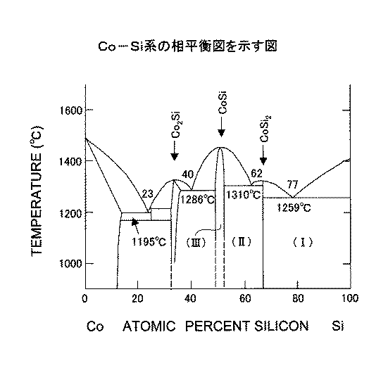
の反応が生じる。このうち、CoSi2のみが低い比抵抗(15−25μΩcm)を有している。
図9は、本発明の原理を示す。
[第1実施例]
図15(A)〜16(F)は、本発明の第1実施例によるMOSトランジスタの製造工程を示す。
[第2実施例]
本発明の第2実施例でも、先に説明した図15(A)〜16(F)と同様の工程により半導体装置の製造を行うが、本実施例では図15(C)の工程において前記TiN保護膜25の堆積を、スパッタパワーを3kWに設定し、窒素ガスおよびArガスをそれぞれ20SCCMおよび100SCCMの流量で供給することにより(N2/Ar比=20/100)、前記TiN保護膜が例えば30nmの膜厚を有するように実行する。ここで、前記スパッタ条件は、Ti/N組成比が1〜5となるようにパワーおよびN2/Ar比を調節され、その結果、得られるTiN保護膜25は、Tiに富んだアモルファス膜となる。
[第3実施例]
本発明の第3実施例でも、先に説明した図15(A)〜16(F)と同様の工程により半導体装置の製造を行うが、本実施例では図15(C)の工程において、前記TiN保護膜25の堆積を、スパッタパワーを9kWに設定し、窒素ガスおよびArガスをそれぞれ90SCCMおよび50SCCMの流量で供給することにより(N2/Ar比=90/50)前記TiN膜25が10nmの厚さに堆積するように実行する。その際、本実施例では前記TiN膜25がナノグレイン構造を有するように形成するために、その膜厚を20nmに設定する。先に説明した図10の関係を参照。
2 Co膜
3 TiN保護膜
11,21 シリコン基板
11A,21A 素子領域
11B,21B 素子分離領域
11W,21W ウェル
11a,21a ソースエクステンション領域
11b,21b ドレインエクステンション領域
11c,21c ソース領域
11d,21d ドレイン領域
11e,11f,13a,21e,21f,23a CoSi2層
12,22 ゲート絶縁膜
13,23 ゲート電極
13A,13B,23A,23B ゲート側壁絶縁膜
14,24 Co膜
15,25 TiN保護膜
111e,111f,113a,121c,121f,123a CoSi層
Claims (10)
- ゲート長が50nm未満の半導体装置の製造方法であって、
半導体基板上に幅が50nm未満のポリシリコンゲート電極パターンを形成する工程と、
前記半導体基板中、前記ポリシリコンゲート電極パターンの両側に一対の拡散領域を形成する工程と、
前記半導体基板上に、前記一対の拡散領域を覆うように、また前記ポリシリコンゲート電極パターンを覆うように、コバルト膜を堆積する工程と、
前記コバルト膜上に、窒化チタン膜を堆積する工程と、
前記窒化チタン膜を堆積する工程の後、前記コバルト膜を、前記ポリシリコンゲート電極の表面および前記一対の拡散領域の表面と反応させ、CoSi2層を形成する工程とよりなり、
前記窒化チタン膜は粒径がその膜厚よりも小さくなるように形成されることを特徴とする半導体装置の製造方法。 - 前記粒径は、10nm以下であることを特徴とする請求項1記載の半導体装置の製造方法。
- ゲート長が50nm未満の半導体装置の製造方法であって、
半導体基板上に幅が50nm未満のポリシリコンゲート電極パターンを形成する工程と、
前記半導体基板中、前記ポリシリコンゲート電極パターンの両側に一対の拡散領域を形成する工程と、
前記半導体基板上に、前記一対の拡散領域を覆うように、また前記ポリシリコンゲート電極パターンを覆うように、コバルト膜を堆積する工程と、
前記コバルト膜上に、窒化チタン膜を堆積する工程と、
前記窒化チタン膜を堆積する工程の後、前記コバルト膜を、前記ポリシリコンゲート電極の表面および前記一対の拡散領域の表面と反応させ、CoSi2層を形成する工程とよりなり、
前記窒化チタン膜はアモルファス相として形成されることを特徴とする半導体装置の製造方法。 - ゲート長が50nm未満の半導体装置の製造方法であって、
半導体基板上に幅が50nm未満のポリシリコンゲート電極パターンを形成する工程と、
前記半導体基板中、前記ポリシリコンゲート電極パターンの両側に一対の拡散領域を形成する工程と、
前記半導体基板上に、前記一対の拡散領域を覆うように、また前記ポリシリコンゲート電極パターンを覆うように、コバルト膜を堆積する工程と、
前記コバルト膜上に、組成がTixNy(x+y=1)で表される窒化チタン膜を堆積する工程と、
前記窒化チタン膜を堆積する工程の後、前記コバルト膜を、前記ポリシリコンゲート電極の表面および前記一対の拡散領域の表面と反応させ、CoSi2層を形成する工程とよりなり、
前記窒化チタン膜はx>yの組成を有することを特徴とする半導体装置の製造方法。 - 前記窒化チタン膜は、1.0<x/y<5.0となるような組成を有することを特徴とする請求項4記載の半導体装置の製造方法。
- 前記窒化チタン膜は、前記CoSi2層中のTi濃度が0.1%以上、1%以下となるように前記組成パラメータx,yを設定されることを特徴とする請求項4または5記載の半導体装置の製造方法。
- 前記窒化チタン膜は20nm以下の膜厚を有することを特徴とする請求項1〜6のうち、いずれか一項記載の半導体装置の製造方法。
- 前記窒化チタン膜は前記コバルト膜に接していることを特徴とする請求項1〜7のうち、いずれか一項記載の半導体装置の製造方法。
- 前記CoSi2層を形成する工程は、前記コバルト膜を前記ポリシリコンゲート電極の表面および前記一対の拡散領域の表面と第1の温度で反応させ、CoSi層を形成する第1の工程と、残留した前記コバルト膜および前記窒化チタン膜を除去する第2の工程と、前記CoSi層をさらに前記ポリシリコンゲート電極の表面および前記一対の拡散領域の表面と第2のより高い温度で反応させ、前記CoSi層を前記CoSi2層に転換させる工程とを含むことを特徴とする請求項1〜8のうち、いずれか一項記載の半導体装置の製造方法。
- 基板と、
前記基板上にゲート絶縁膜を介して形成された、ゲート長が50nm以下のポリシリコンゲート電極と、
前記基板中、前記ポリシリコンゲート電極の両側において、前記ポリシリコンゲート電極の側壁絶縁膜の外側に形成された一対の拡散領域とよりなる半導体装置であって、
前記ポリシリコンゲート電極の上面および前記一対の拡散領域の表面にはCoSi2層が形成されており、
前記CoSi2層はTiを、0.1〜1.0原子パーセントの濃度で含むことを特徴とする半導体装置。
Priority Applications (2)
| Application Number | Priority Date | Filing Date | Title |
|---|---|---|---|
| JP2004299280A JP2006114633A (ja) | 2004-10-13 | 2004-10-13 | 半導体装置の製造方法 |
| US11/041,217 US20060079087A1 (en) | 2004-10-13 | 2005-01-25 | Method of producing semiconductor device |
Applications Claiming Priority (1)
| Application Number | Priority Date | Filing Date | Title |
|---|---|---|---|
| JP2004299280A JP2006114633A (ja) | 2004-10-13 | 2004-10-13 | 半導体装置の製造方法 |
Publications (1)
| Publication Number | Publication Date |
|---|---|
| JP2006114633A true JP2006114633A (ja) | 2006-04-27 |
Family
ID=36145916
Family Applications (1)
| Application Number | Title | Priority Date | Filing Date |
|---|---|---|---|
| JP2004299280A Pending JP2006114633A (ja) | 2004-10-13 | 2004-10-13 | 半導体装置の製造方法 |
Country Status (2)
| Country | Link |
|---|---|
| US (1) | US20060079087A1 (ja) |
| JP (1) | JP2006114633A (ja) |
Cited By (2)
| Publication number | Priority date | Publication date | Assignee | Title |
|---|---|---|---|---|
| KR100776174B1 (ko) * | 2006-08-24 | 2007-11-12 | 동부일렉트로닉스 주식회사 | 실리사이드를 포함하는 반도체 소자 및 그 제조방법 |
| JP2012528488A (ja) * | 2009-05-28 | 2012-11-12 | コヴィオ インコーポレイテッド | 拡散バリアで被覆された基板上の半導体デバイス及びその形成方法 |
Families Citing this family (4)
| Publication number | Priority date | Publication date | Assignee | Title |
|---|---|---|---|---|
| CN102122613A (zh) * | 2010-01-08 | 2011-07-13 | 中芯国际集成电路制造(上海)有限公司 | 自对准金属硅化物的形成方法 |
| CN103515217A (zh) * | 2012-06-26 | 2014-01-15 | 中芯国际集成电路制造(上海)有限公司 | 金属硅化物层的形成方法和nmos晶体管的形成方法 |
| US10811262B2 (en) | 2016-01-14 | 2020-10-20 | Taiwan Semiconductor Manufacturing Co., Ltd. | Semiconductor device having a uniform and thin silicide layer on an epitaxial source/ drain structure and manufacturing method thereof |
| EP4376054A1 (fr) * | 2022-11-23 | 2024-05-29 | EM Microelectronic-Marin SA | Procédé de réalisation d'un circuit intégré pour pallier des défauts ou des dislocations |
Family Cites Families (5)
| Publication number | Priority date | Publication date | Assignee | Title |
|---|---|---|---|---|
| US6104525A (en) * | 1997-04-29 | 2000-08-15 | Daewoo Electronics Co., Ltd. | Array of thin film actuated mirrors and method for the manufacture thereof |
| JP3523093B2 (ja) * | 1997-11-28 | 2004-04-26 | 株式会社東芝 | 半導体装置およびその製造方法 |
| US20020061639A1 (en) * | 2000-10-02 | 2002-05-23 | Kazuichiroh Itonaga | Semiconductor device and method for manufacturing the same |
| JP2004140315A (ja) * | 2002-10-17 | 2004-05-13 | Samsung Electronics Co Ltd | サリサイド工程を用いる半導体素子の製造方法 |
| US6936528B2 (en) * | 2002-10-17 | 2005-08-30 | Samsung Electronics Co., Ltd. | Method of forming cobalt silicide film and method of manufacturing semiconductor device having cobalt silicide film |
-
2004
- 2004-10-13 JP JP2004299280A patent/JP2006114633A/ja active Pending
-
2005
- 2005-01-25 US US11/041,217 patent/US20060079087A1/en not_active Abandoned
Cited By (2)
| Publication number | Priority date | Publication date | Assignee | Title |
|---|---|---|---|---|
| KR100776174B1 (ko) * | 2006-08-24 | 2007-11-12 | 동부일렉트로닉스 주식회사 | 실리사이드를 포함하는 반도체 소자 및 그 제조방법 |
| JP2012528488A (ja) * | 2009-05-28 | 2012-11-12 | コヴィオ インコーポレイテッド | 拡散バリアで被覆された基板上の半導体デバイス及びその形成方法 |
Also Published As
| Publication number | Publication date |
|---|---|
| US20060079087A1 (en) | 2006-04-13 |
Similar Documents
| Publication | Publication Date | Title |
|---|---|---|
| US6562718B1 (en) | Process for forming fully silicided gates | |
| US7397091B2 (en) | SiGe nickel barrier structure employed in a CMOS device to prevent excess diffusion of nickel used in the silicide material | |
| JP5672334B2 (ja) | 半導体装置の製造方法 | |
| CN100336186C (zh) | 形成硅化镍层以及半导体器件的方法 | |
| US7396767B2 (en) | Semiconductor structure including silicide regions and method of making same | |
| JP2586345B2 (ja) | コバルトシリサイド膜より成る半導体装置及び該装置の製造方法 | |
| US20070128867A1 (en) | Method for enhanced uni-directional diffusion of metal and subsequent silicide formation | |
| JP5813313B2 (ja) | 半導体を含む金属材料の形成方法 | |
| US7495293B2 (en) | Semiconductor device and method for manufacturing the same | |
| JPWO2007026677A1 (ja) | 半導体装置の製造方法 | |
| JP4146859B2 (ja) | 半導体装置の製造方法 | |
| JPH11214327A (ja) | コバルト/ニオブ二重金属層構造を利用したシリサイド形成方法 | |
| JP3492973B2 (ja) | 半導体装置の製造方法 | |
| JP2006114633A (ja) | 半導体装置の製造方法 | |
| JP2930042B2 (ja) | 半導体装置の製造方法 | |
| JP2001053027A (ja) | 半導体装置の製造方法 | |
| JP2586407B2 (ja) | 半導体装置の製造方法 | |
| JP4525896B2 (ja) | 半導体装置の製造方法 | |
| JP2009094395A (ja) | 半導体装置およびその製造方法 | |
| JP5195421B2 (ja) | 半導体装置 | |
| JPH0878358A (ja) | 半導体装置の製造方法 | |
| JPH09320985A (ja) | 半導体装置および該半導体装置の製造方法 | |
| JP3816918B2 (ja) | 半導体装置及びその製造方法 | |
| JP2001077127A (ja) | 化合物半導体装置及びその製造方法 | |
| JP2004158878A (ja) | 半導体装置の製造方法 |
Legal Events
| Date | Code | Title | Description |
|---|---|---|---|
| A621 | Written request for application examination |
Free format text: JAPANESE INTERMEDIATE CODE: A621 Effective date: 20060222 |
|
| A977 | Report on retrieval |
Free format text: JAPANESE INTERMEDIATE CODE: A971007 Effective date: 20071022 |
|
| A131 | Notification of reasons for refusal |
Free format text: JAPANESE INTERMEDIATE CODE: A131 Effective date: 20071030 |
|
| A521 | Request for written amendment filed |
Free format text: JAPANESE INTERMEDIATE CODE: A523 Effective date: 20071228 |
|
| A02 | Decision of refusal |
Free format text: JAPANESE INTERMEDIATE CODE: A02 Effective date: 20080311 |